Embed Size (px)
Citation preview
CHAPTER 12
IMPEDANCE SPECTROSCOPY: A GENERAL INTRODUCTION AND APPLICATION TO
DYE-SENSITIZED SOLAR CELLS
Juan Bisquert and Francisco Fabregat-Santiago
12.1 INTRODUCTION
Impedance Spectroscopy (IS) has become a major tool for investigating the properties and quality of dye-sensitized solar cell (DSC) devices. This chapter provides an intro-duction of IS interpretation methods focusing on the analysis of DSC impedance data. It also presents a scope of the main results obtained so far. IS gives access to funda-mental mechanisms of operation of solar cells, for which reason we discuss our views of basic photovoltaic principles required to realize the interpretation of the experi-mental results. The chapter summarizes some 10 years of experience of the authors with regard to modeling, measurement and interpretation of IS applied in DSC.
A good way to start this subject is a brief recollection of how it evolved over the fi rst years. The original “standard” confi guration of a DSC [12.1] that emerged in the early 1990s is formed by a large internal area constituted of a nanostructured TiO2 semiconductor, connected to a transparent conducting oxide (TCO) and coated with photoactive dye molecules. It is furthermore in contact with a redox I I−
3−/ electrolyte
that is in turn connected to a Pt-catalyzed counterelectrode (CE). The DSC was ini-tially developed to be a photoelectrochemical solar cell. Electrochemical Impedance Spectroscopy (EIS) is a traditional method, central to electrochemical science and technology. Electrochemistry usually investigates interfacial charge transfer between a solid conductor (the working electrode, WE) and an electrolyte. This is done with a voltage applied between the WE and CE, with the assistance of a reference electrode (RE), rendering it possible to identify the voltage drop at the interface between the WE and the electrolyte. In addition, the electrolyte often contains a salt that provides a large conductivity in the liquid phase and removes limitations by drift transport in an electrical fi eld. Electrochemistry is thus mostly concerned with interfacial charge transfer events, possibly governed by diffusion of reactants or products. It is with EIS
2 Dye-sensitized solar cells
possible to readily separate the interfacial capacitance and charge-transfer resistance, as well as to identify diffusion components in the electrolyte. A good introduction to such applications is given by Gabrielli [12.2].
In solid state solar cell science and technology, the most commonly applied frequency technique is Admittance Spectroscopy (AS). By tradition, AS denominates a special method that operates at reverse voltage and evaluates the energy levels of majority carrier traps (in general, all those that cross the Fermi level) as well as trap densities of states [12.3]. In work on DSCs and other solar cells, we may be interested to probe a wide variety of conditions. Consequently, we generally use the denomina-tion Impedance Spectroscopy (IS) when referring to the technique applied in this context (rather than EIS or AS).
Before the advent of DSC, IS had been largely applied in photoelectrochem-istry [12.4, 12.5]. This is a fi eld widely explored since the 1970s, using compact monocrystalline or polycrystalline semiconductor electrodes for sunlight energy con-version [12.6-12.8]. In these systems, IS provides information on the electronic car-rier concentration at the surface, via Mott-Schottky plots (i.e., the reciprocal square capacitance versus the bias voltage) as well as on the rates of interfacial charge trans-fer [12.9-12.11]. Several important concepts, later to be applied in DSC, where estab-lished at that time, such as the bandedge shift by charging of the Helmholtz layer and the crucial role of surface states in electron or hole transfer to acceptors in solution [12.9, 12.10, 12.12-12.14]. Nonetheless, it was clearly recognized that applying IS in these systems is far from trivial, for example due to the presence of frequency disper-sion that complicates the determination of parameters [12.15]
It was natural to apply such well-established electrochemical methods to DSC and several groups have done so [12.16-12.19]. However, in the early studies, it was necessary to clarify a conceptual framework of interpretation which took several years. On the one hand, the early diffusion-recombination model [12.20] was generally adopted for steady-state techniques and produced very good results when extended to light-modulated frequency techniques [12.21]. In this approach, the only role of the applied voltage is to establish the concentration of electrons at the edge of the TiO2 in contact with TCO [12.20, 12.21]. On the other hand, classical photoelectrochemical methods heavily rest on the notion of charge collection at the surface space-charge layer, while diffusion is viewed as an auxiliary component, at best [12.22]. Thus, in photoelectrochemistry of compact semiconductor electrodes, the main method to describe the system behavior is an understanding of the electric potential distribution between the bulk semiconductor and the semiconductor/electrolyte interface [12.7].
Owing to these confl icting approaches, in the DSC area there were many discus-sions concerning the distribution of the applied voltage as internal “potential drops”, the origin of photovoltage, screening, and the role of electron-hole separation at the space-charge region [12.23-12.27]. This is understandable since the DSC is a porous, heterogeneous system, and in models of systems with a complex morphology, it is generally diffi cult to match diffusion control with a precise statement regarding the electrical potential distribution. The key element for progress is to adopt a macro-homogeneous approach and focus in the spatial distribution of the Fermi level. This method emerged in the DSC area [12.24, 12.28-12.30] and eventually led to gener-alized photovoltaic principles based on the splitting of Fermi levels and the crucial
Impedance spectroscopy 3
role of selective contacts [12.31-12.34]. Another central concept that appeared in the DSC area was a “conduction band capacitance” [12.26, 12.28, 12.30], later to be generally defi ned as a chemical capacitance [12.35]. This capacitive element is nor-mally absent in classical photoelectrochemistry but is key for the interpretation of frequency-resolved techniques in DSC. Also important was the recognition [12.26, 12.36] that nanostructured TiO2 should be treated as a disordered material, much like the amorphous semiconductors [12.37-12.39], with electronic traps affecting not only the surface events, but any differential/kinetic measurements, including the chemical capacitance [12.35], recombination lifetime and transport coeffi cients [12.40].
The passage from established ideas of photoelectrochemistry to those best suited to the DSC have inevitably rendered it necessary to treat the porous-mixed phase structure of the DSC. Electrochemistry was already evolving in this direction for some decades, fi rst with the description of porous electrodes [12.41], and then, with the introduction of truly active electrodes that become modifi ed under bias voltage, such as intercalation metal-oxides [12.42], conducting polymers [12.43] and redox polymers [12.44]. Especially important is the work of Chidsey and Murray [12.44], which shows the modifi cation of the diffusion coeffi cient in the solid phase, as well as the capacitance of the solid material as a whole, in opposition to the standard interfa-cial capacitance. In the analysis of these systems, either porous or not, the importance of coupling transport elements with interfacial and/or recombination components for a proper description of IS data was well recognized. Transmission line models pro-vide a natural representation of the IS models and are widely used [12.43, 12.45].
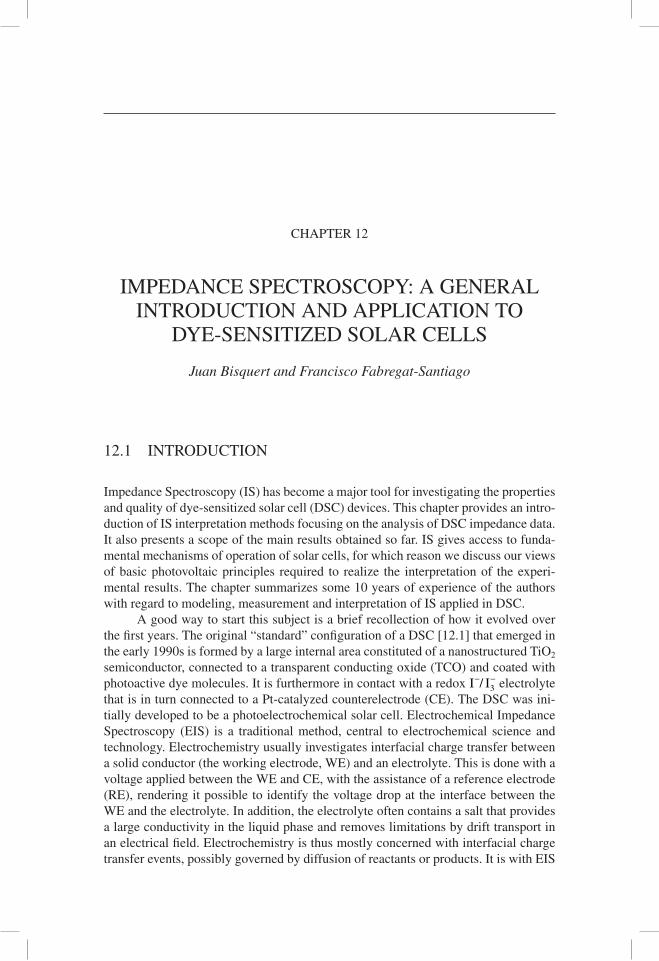
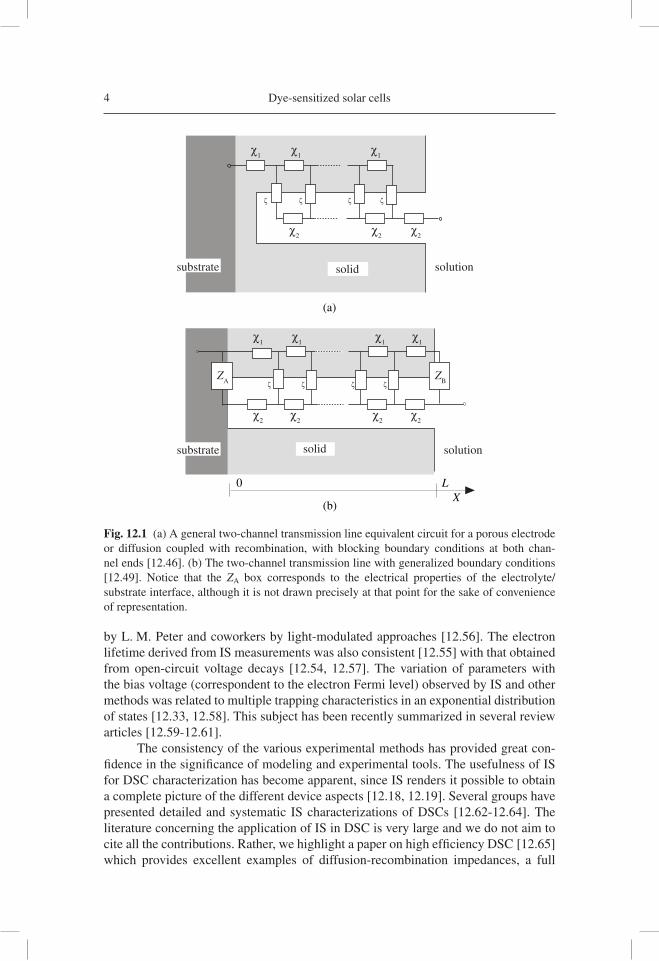
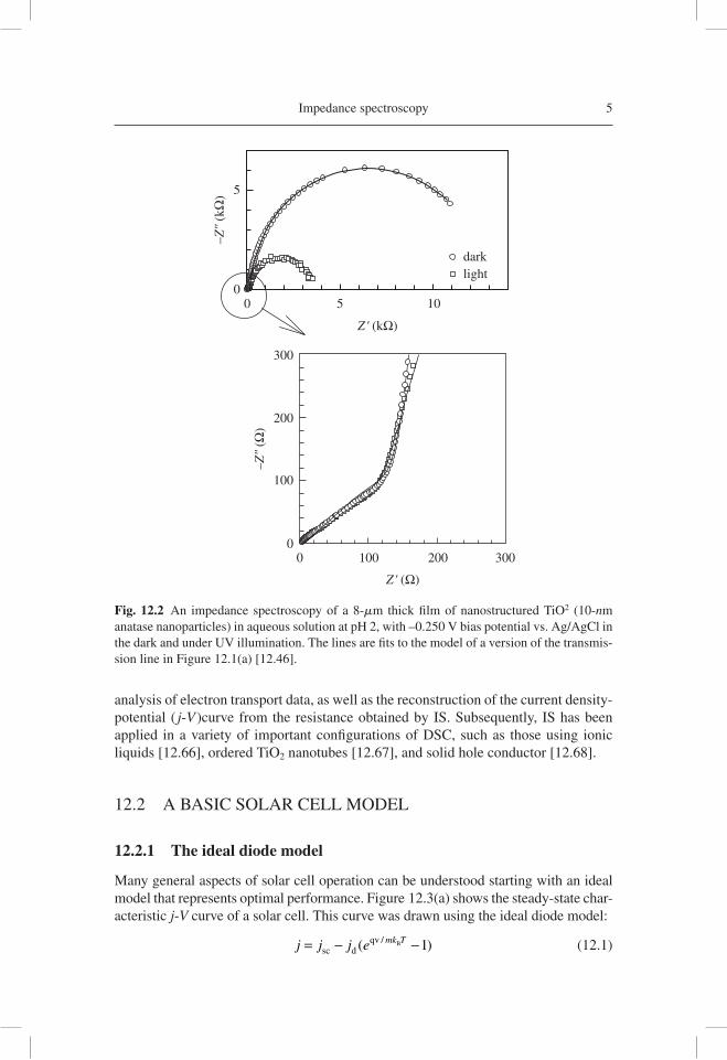
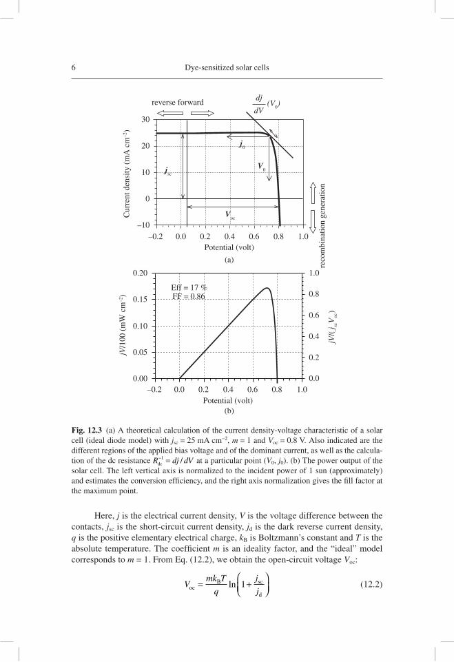
As demonstrated in Figure 12.1, transmission line models incorporating fre-quency dispersion, which is ubiquitous in disordered materials, have been developed and applied to nanostructured TiO2 used in DSC. A very good realization of the model was soon found in the experiment, as shown in Figure 12.2 [12.46]. Later, diffusion-reaction models were solved for IS characterization, and the models where put in rela-tion to both nanostructured semiconductors and bulk semiconductors for solar cells [12.47]. Disorder was included also in generalized transmission lines for anomalous diffusion [12.48]. In addition, the role of macroscopic contacts was analyzed in gen-eralized transmission line models, as shown in Figure 12.1(b) [12.49], and this effect would take relevance as a result of the TCO contribution to the measured impedance [12.50, 12.51].
The calculation of the diffusion-recombination impedance [12.47] opened the way for a direct measurement of conductivity of electrons in TiO2 by IS [12.52], which provided a good validation of the method. Further, the diffusion- recombination impedance also naturally reveals [12.47] the chemical capacitance of electrons in nanostructured TiO2 (associated to the rise of the Fermi level), which also appears in measurements of cyclic voltammetry (at slow scan rates) [12.53] and electron lifetime [12.54].
Application of these IS methods and models to DSC [12.51] demonstrated that IS provides a picture of the energetics of TiO2, which is a crucial tool for compar-ing DSC confi gurations [12.55]. It also showed that it was possible to simultane-ously obtain the parameters for transport and recombination at various steady-state conditions of a DSC, which is an unsurpassed power of the technique. The trends of the electron diffusion coeffi cient [12.51] where similar to those found previously
4 Dye-sensitized solar cells
by L. M. Peter and coworkers by light-modulated approaches [12.56]. The electron lifetime derived from IS measurements was also consistent [12.55] with that obtained from open-circuit voltage decays [12.54, 12.57]. The variation of parameters with the bias voltage (correspondent to the electron Fermi level) observed by IS and other methods was related to multiple trapping characteristics in an exponential distribution of states [12.33, 12.58]. This subject has been recently summarized in several review articles [12.59-12.61].
The consistency of the various experimental methods has provided great con-fi dence in the signifi cance of modeling and experimental tools. The usefulness of IS for DSC characterization has become apparent, since IS renders it possible to obtain a complete picture of the different device aspects [12.18, 12.19]. Several groups have presented detailed and systematic IS characterizations of DSCs [12.62-12.64]. The literature concerning the application of IS in DSC is very large and we do not aim to cite all the contributions. Rather, we highlight a paper on high effi ciency DSC [12.65] which provides excellent examples of diffusion-recombination impedances, a full
substrate solid solution
substrate solid solution
χ2
χ2
χ2
χ1
χ1
χ1
ζ ζ ζ ζ
χ1
χ2
χ2
χ2
χ2
χ1
χ1
χ1
ζ ζ ζ ζZ
AZ
B
0 LX
(b)
(a)
Fig. 12.1 (a) A general two-channel transmission line equivalent circuit for a porous electrode or diffusion coupled with recombination, with blocking boundary conditions at both chan-nel ends [12.46]. (b) The two-channel transmission line with generalized boundary conditions [12.49]. Notice that the ZA box corresponds to the electrical properties of the electrolyte/ substrate interface, although it is not drawn precisely at that point for the sake of convenience of representation.
Impedance spectroscopy 5
analysis of electron transport data, as well as the reconstruction of the current density-potential ( j-V )curve from the resistance obtained by IS. Subsequently, IS has been applied in a variety of important confi gurations of DSC, such as those using ionic liquids [12.66], ordered TiO2 nanotubes [12.67], and solid hole conductor [12.68].
12.2 A BASIC SOLAR CELL MODEL
12.2.1 The ideal diode model
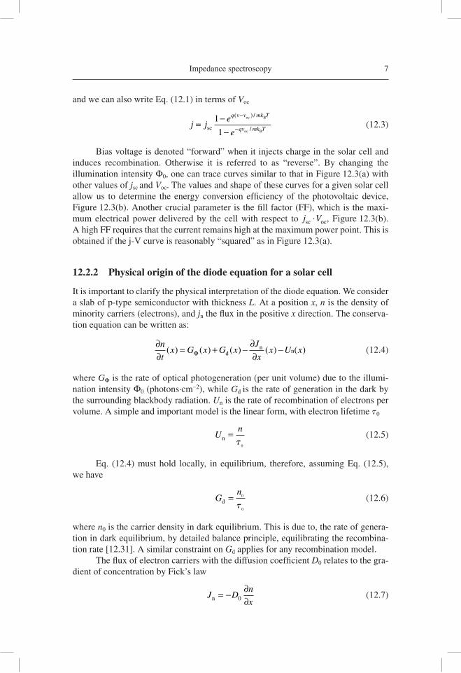
Many general aspects of solar cell operation can be understood starting with an ideal model that represents optimal performance. Figure 12.3(a) shows the steady-state char-acteristic j-V curve of a solar cell. This curve was drawn using the ideal diode model:
j j j mk T= − −sc dB( )/eqv 1 (12.1)
5
–Z"
(kΩ
)
–Z"
(Ω)
Z' (kΩ)
0
300
200
100
00 100 200 300
0 5 10
darklight
Z' (Ω)
Fig. 12.2 An impedance spectroscopy of a 8-mm thick fi lm of nanostructured TiO2 (10-nm anatase nanoparticles) in aqueous solution at pH 2, with –0.250 V bias potential vs. Ag/AgCl in the dark and under UV illumination. The lines are fi ts to the model of a version of the transmis-sion line in Figure 12.1(a) [12.46].
6 Dye-sensitized solar cells
Here, j is the electrical current density, V is the voltage difference between the contacts, jsc is the short-circuit current density, jd is the dark reverse current density, q is the positive elementary electrical charge, kB is Boltzmann’s constant and T is the absolute temperature. The coeffi cient m is an ideality factor, and the “ideal” model corresponds to m = 1. From Eq. (12.2), we obtain the open-circuit voltage Voc:
Vmk T
q
j
jocB sc
d
= +⎛⎝⎜
⎞⎠⎟
ln 1 (12.2)
reverse forwarddj
dV(V
0)
Eff = 17 %FF = 0.86
jV/1
00 (
mW
cm
–2)
jV/(
j scV
oc)
0.20
0.15
0.10
0.05
0.00–0.2 0.0 0.2 0.4 0.6 0.8 1.0
0.0
0.2
0.4
0.6
0.8
1.0
Potential (volt)
(a)
(b)
Cur
rent
den
sity
(m
A c
m–2
)
reco
mbi
natio
n ge
nera
tion
–0.2 0.0 0.2 0.4 0.6 0.8 1.0–10
0
10
20
30
jsc
j0
V0
Voc
Potential (volt)
Fig. 12.3 (a) A theoretical calculation of the current density-voltage characteristic of a solar cell (ideal diode model) with jsc = 25 mA cm−2, m = 1 and Voc = 0.8 V. Also indicated are the different regions of the applied bias voltage and of the dominant current, as well as the calcula-tion of the dc resistance R dj dVdc
− =1 / at a particular point (V0, j0). (b) The power output of the solar cell. The left vertical axis is normalized to the incident power of 1 sun (approximately) and estimates the conversion effi ciency, and the right axis normalization gives the fi ll factor at the maximum point.
Impedance spectroscopy 7
and we can also write Eq. (12.1) in terms of Voc
j j
q v v mk T
qv mk T= −
−
−
−sc
oc B
oc B
1
1
e
e
( ) /
/ (12.3)
Bias voltage is denoted “forward” when it injects charge in the solar cell and induces recombination. Otherwise it is referred to as “reverse”. By changing the illumination intensity Φ0, one can trace curves similar to that in Figure 12.3(a) with other values of jsc and Voc. The values and shape of these curves for a given solar cell allow us to determine the energy conversion effi ciency of the photovoltaic device, Figure 12.3(b). Another crucial parameter is the fi ll factor (FF), which is the maxi-mum electrical power delivered by the cell with respect to j Vsc oc⋅ , Figure 12.3(b). A high FF requires that the current remains high at the maximum power point. This is obtained if the j-V curve is reasonably “squared” as in Figure 12.3(a).
12.2.2 Physical origin of the diode equation for a solar cell
It is important to clarify the physical interpretation of the diode equation. We consider a slab of p-type semiconductor with thickness L. At a position x, n is the density of minority carriers (electrons), and jn the fl ux in the positive x direction. The conserva-tion equation can be written as:
∂∂
= + − −n
tx G x G x
J
xx U x( ) ( ) ( ) ( ) ( )Φ
∂∂d
nn (12.4)
where GΦ is the rate of optical photogeneration (per unit volume) due to the illumi-nation intensity Φ0 (photons·cm−2), while Gd is the rate of generation in the dark by the surrounding blackbody radiation. Un is the rate of recombination of electrons per volume. A simple and important model is the linear form, with electron lifetime t0
U
nn =t
0
(12.5)
Eq. (12.4) must hold locally, in equilibrium, therefore, assuming Eq. (12.5), we have
G
nd = 0
0t
(12.6)
where n0 is the carrier density in dark equilibrium. This is due to, the rate of genera-tion in dark equilibrium, by detailed balance principle, equilibrating the recombina-tion rate [12.31]. A similar constraint on Gd applies for any recombination model.
The fl ux of electron carriers with the diffusion coeffi cient D0 relates to the gra-dient of concentration by Fick’s law
J D
n
xn = − ∂∂0 (12.7)
8 Dye-sensitized solar cells
While Eq. (12.4) can be solved for any kind of generation profi le and bound-ary conditions, we now adopt certain assumptions that lead to the central diode model (12.1) in the simplest way. We assume that the photogeneration of carriers is homogeneous, and we consider that the transport of electrons is very fast. It can thus be assumed that D0 is extremely large, implying that the gradient of concentration required to maintain the fl ux is very small. With these assumptions all the quantities in Eq. (12.4), except the carrier fl ux, become independent of position. We now integrate between 0 ≤ x ≤?? and obtain
∂∂
= + − − −n
tG G
LJ L J UΦ d n n n
10[ ( ) ( )] (12.8)
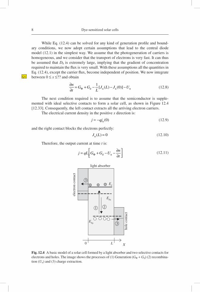
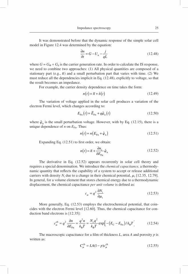
The next condition required is to assume that the semiconductor is supple-mented with ideal selective contacts to form a solar cell, as shown in Figure 12.4 [12.33]. Consequently, the left contact extracts all the arriving electron carriers.
The electrical current density in the positive x direction is:
j qj= − n ( )0 (12.9)
and the right contact blocks the electrons perfectly:
J Ln ( ) = 0 (12.10)
Therefore, the output current at time t is:
j qL G G U
n
t= + − − ∂
∂⎡⎣⎢
⎤⎦⎥Φ d n
(12.11)
Q1Q1
light absorber
elec
tron
con
tact
hole
con
tact
EC
EFn
EFp
3
2
3
0 L X
1
Fig. 12.4 A basic model of a solar cell formed by a light absorber and two selective contacts for electrons and holes. The image shows the processes of (1) Generation (GΦ + Gd) (2) recombina-tion (Un) and (3) charge extraction.
Impedance spectroscopy 9
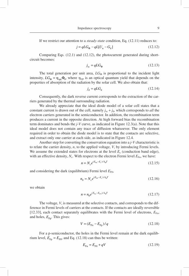
If we restrict our attention to a steady-state condition, Eq. (12.11) reduces to:
j qLG qL U G= − −Φ [ ]n d (12.12)
Comparing Eqs. (12.1) and (12.12), the photocurrent generated during short-circuit becomes:
j qLGsc = Φ (12.13)
The total generation per unit area, LGΦ is proportional to the incident light intensity, LGΦ Φ= hopt 0, where hopt is an optical quantum yield that depends on the properties of absorption of the radiation by the solar cell. We also obtain that:
j qLGd d= (12.14)
Consequently, the dark reverse current corresponds to the extraction of the car-riers generated by the thermal surrounding radiation.
We already appreciate that the ideal diode model of a solar cell states that a constant current is drawn out of the cell, namely jsc + jd, which corresponds to all the electron carriers generated in the semiconductor. In addition, the recombination term produces a current in the opposite direction. At high forward bias the recombination term dominates and bends the j-V curve, as indicated in Figure 12.3(a). Note that this ideal model does not contain any trace of diffusion whatsoever. The only element required in order to obtain the diode model is to state that the contacts are selective, and extract only one carrier at each side, as indicated in Figure 12.4.
Another step for converting the conservation equation into a j-V characteristic is to relate the carrier density, n, to the applied voltage, V, by introducing Fermi levels. We assume the extended states for electrons at the level Ec (conduction band edge), with an effective density, Nc. With respect to the electron Fermi level EFn, we have:
n N e E E k T= −c
Fn c B( ) / (12.15)
and considering the dark (equilibrium) Fermi level EF0,
n N e E E k T0 = −
cF0 c B( ) / (12.16)
we obtain
n n e E E k T= −0
0( ) /Fn F B (12.17)
The voltage, V, is measured at the selective contacts, and corresponds to the dif-ference in Fermi levels of carriers at the contacts. If the contacts are ideally reversible [12.33], each contact separately equilibrates with the Fermi level of electrons, EFn, and holes, EFp. This gives:
V E E q= −( ) /Fn Fp (12.18)
For a p-semiconductor, the holes in the Fermi level remain at the dark equilib-rium level, E EFp F0= , and Eq. (12.18) can thus be written:
E E qVFn F0= + (12.19)
10 Dye-sensitized solar cells
In consequence:
n n e= 0qV k T/ B (12.20)
Using the linear recombination of Eq. (12.5) in Eq. (12.12), and applying the Boltzmann statistics indicated in Eq. (12.20), we obtain the diode equation (12.1) with m = 1. However, if we assume a nonlinear recombination model, more general than the one used previously
U k nn r= b (12.21)
we obtain the general diode equation with m = 1/b. Here, Eq. (12.21) is written as a purely empirical law, but its origin is further discussed below.
It should be noted that the recombination mechanism has a major impact on the shape of the j-?? curve, especially on the FF. Therefore also on the solar cell conver-sion effi ciency. In fact, as we have shown with the above model, for ideal selective contacts, the diode ideality factor m is entirely determined by the bulk recombination mechanism. This point is well understood in solid-state electronics [12.69].
12.3 INTRODUCTION TO IS METHODS
In general, IS is applied to a system with electrical contacts. It consists of a measure-ment of the ac electrical current, ˆ( )I v , at a certain angular frequency, v, when a cer-tain ac voltage, ˆ ( )V v , is applied to the system, or vice versa, a measurement of ˆ ( )V v at an applied Î(v). The impedance is:
Z
V
Iv
v
v( ) =
( )( )
ˆ
ˆ (10.22)
The symbol x over a quantity x indicates that x is:
(1) the complex amplitude of a sinusoidal (ac) perturbation of x and
(2) a small perturbation.
The “smallness” of x is required in order to obtain the linear impedance in Eq. (12.22), i.e., Î(v) is linear with respect to ˆ ( )V v , or vice versa, so that Z(v) is inde-pendent of the amplitude of the perturbation. In modeling work, this is ensured if the absolute value of ??x?? is much lower than that of the steady state quantities ??x??, ??y??, … In practice this means that the amplitude of the voltage must be on the order of several mV. However, in certain situations, e.g., close to a phase transition, a small perturbation of the voltage induces very large variations of the charge or current, and the conditions of linearity must thus be carefully inquired.
During an impedance measurement, the system is (ideally) kept at a fi xed steady state by imposing stationary constraints such as the dc current, illumination intensity, etc., and the Z(v) is measured by scanning the frequency at a multitude of values
Q1Q1
Q1Q1
Impedance spectroscopy 11
f = v/2p, typically over several decades, i.e., from mHz to 10 MHz, with 5-10 meas-urements per decade. At each frequency the impedance meter must verify that the Z(v) is stable. At low frequencies, this takes a considerable amount of time, i.e., stabilizing a measurement at f = 10 mHz consumes minutes. Nevertheless, measurements at low frequencies are often important in order to make sure that one is approaching the dc regime, as further explained below. A judicious selection of the frequency window of measurement is therefore necessary, and this is often aided by experience.
In addition to scanning the frequencies, it is usually very important to deter-mine the IS parameters at various conditions of steady state. This is the key approach in order to relate the measurement to a given physical model. At each steady state the Z(v) data is related to a model in the frequency domain, which is usually represented as an equivalent circuit. By modifying the steady state, the change in impedance parameters (resistances, capacitances, etc.) can be monitored in relation to the physi-cal properties of the system. Since the impedance measurement takes a considerable amount of time, the steady state often changes along the impedance measurement, and precautions should be taken to avoid a serious drift of the parameters. In par-ticular, care should be taken with unintentional changes of temperature in solar cells, since this introduces additional and unwanted variations of the parameters.
Note that, at each steady state, a full scan of frequencies is necessary. Thus many steady state points imply a long measurement, perhaps over an entire day. However, data that do not cover different steady states may in some cases be of little value, particularly if there is uncertainty regarding the meaning of the parameters. It is also important to verify the true signifi cance of parameters by material varia-tions of the samples, e.g., to confi rm the correlation of a transport resistance with the reciprocal length of the sample. The extent to which these approaches must be judiciously realized depends on the preliminary knowledge and experience of the particular system.
12.3.1 Steady state and small perturbation quantities
As an example of the relationship between the ac impedance and steady-state quan-tities, we discuss a characteristic experiment on a solar cell using the ideal model outlined in Figures 12.3 and 12.4. We choose a certain point of bias voltage, V0, with the associated current density, j0. At this point, a small displacement of voltage ˆ ( )V 0 implies a change of current ˆ( )j 0 . The value v = 0 in parenthesis indicates that the displacement is infi nitely slow, i.e., ˆ ( )V 0 and ˆ( )j 0 attain a value that is independent of time. The displacement of the current and voltage is indicated in Figure 12.3(a) with arrows.
For a solar cell with area A, the quotient of the small quantities gives:
Z
V
Aj
Adj
dVR0
0
0
1
( ) =( )( ) = ⎛
⎝⎜⎞⎠⎟
=−ˆ
ˆ dc (12.23)
In other words, the small quantities provide a derivative of the voltage with respect to the current. This is the reciprocal of the slope of the j-V curve, which is in turn the dc resistance of the solar cell Rdc (per area) under those particular conditions.
12 Dye-sensitized solar cells
A similar process occurs if we measure the change in the electrical charge, Q, under a perturbation of the voltage. The quotient is a capacitance:
ˆ ( )ˆ ( )
Q
V
dQ
dVC
0
0= = (12.24)
In general, the parameters obtained by IS are related to derivatives of the steady state variables describing the system, i.e., IS provides the differential resistance, dif-ferential capacitance, etc. However, we usually omit the specifi cation of “differential” in the context of IS as it is implicitly assumed.
It is useful to observe that, since Rdc is the reciprocal of the slope of the cur-rent density-potential curve, Figure 12.3(a), knowledge of Rdc at several points allows us to construct the full curve, provided that a single point of the curve is known (for example, the value of jsc):
j V j R dV
V( ) = − −∫sc dc
1
0 (12.25)
Therefore, understanding the different elements that determine Rdc is a key step in order to analyze the factors governing the effi ciency of the solar cell.
From the steady state characteristic, we can only derive Z(0), i.e., the imped-ance at the frequency v = 0. However, in order to understand the operation of the solar cell we wish to know the origin of Rdc in terms of the internal processes occurring in the device: transport of charges, accumulation at certain points, recombination of car-riers, and so on. Eventually, we are interested also in the dynamic behavior of the solar cell, i.e., how it responds with time to a certain perturbation.
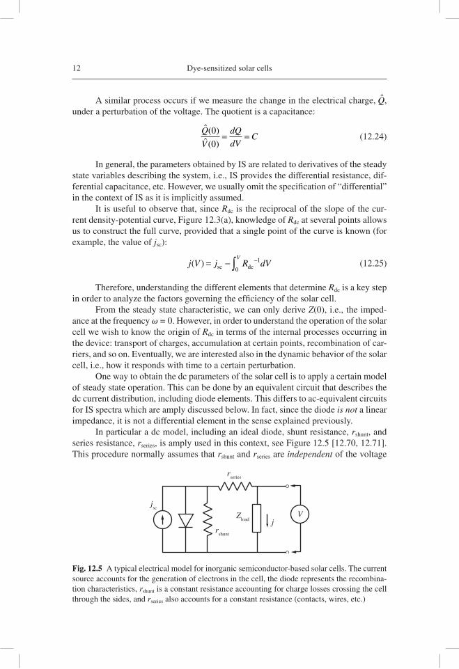
One way to obtain the dc parameters of the solar cell is to apply a certain model of steady state operation. This can be done by an equivalent circuit that describes the dc current distribution, including diode elements. This differs to ac-equivalent circuits for IS spectra which are amply discussed below. In fact, since the diode is not a linear impedance, it is not a differential element in the sense explained previously.
In particular a dc model, including an ideal diode, shunt resistance, rshunt, and series resistance, rseries, is amply used in this context, see Figure 12.5 [12.70, 12.71]. This procedure normally assumes that rshunt and rseries are independent of the voltage
rseries
Zload j
V
rshunt
jsc
Fig. 12.5 A typical electrical model for inorganic semiconductor-based solar cells. The current source accounts for the generation of electrons in the cell, the diode represents the recombina-tion characteristics, rshunt is a constant resistance accounting for charge losses crossing the cell through the sides, and rseries also accounts for a constant resistance (contacts, wires, etc.)
Impedance spectroscopy 13
along the j-V characteristics. Such an assumption may work well in some classes of solar cells such as monocrystalline Si solar cells. However, in other cases, especially in devices including electrochemical processes such as in DSC, it is far from clear that resistances remain constant, even at reverse voltage. Great care should be taken when applying dc models to DSC, since one may impose a model that does not occur in the device and the results of which may have little meaning.
We demonstrate later how to construct a dc model that is normally useful for the analysis of DSC, but fi rst we need to discuss the origin of the elements that appear in equivalent circuits. To this end, we describe a much more powerful approach, apply-ing IS, in order to obtain all the stationary and dynamic information concerning the current-voltage behavior of the system.
12.3.2 The frequency domain
In general, the method of IS, consists in measuring the quotient in Eq. (12.22), for a signal ˆ ( )V v varying at different angular velocities. When the velocity, v, is very slow, we are close to steady state conditions and obtain exactly the dc resistance as indi-cated in Eq. (12.23). However, when v becomes faster, certain processes in the system are unable to respond to the applied perturbation. Z(v) therefore contains contribu-tions from “things faster than” v.
By scanning the frequency, we obtain a changing response (the impedance spec-trum) that can be treated by several methods (analytical, numerical, and most impor-tantly, by visual inspection of its shape) in order to provide a detailed physical picture of the dynamic properties of the system. In particular, it is essential for solar cell applications that this method renders it possible to dissect the steady-state response into its elementary components. A vivid explanation of the physics and an interpreta-tion of the electrical magnitudes in the frequency domain for dielectric materials is given in the book Dielectric Relaxation in Solids by A.K. Jonscher [12.72].
One may wonder why one should use so many different angular frequencies in the measurement, when the same processes can be probed by time transients, i.e., by applying a voltage step and monitoring the subsequent evolution towards equilibrium. This way, the fast and progressively slower processes in the system can be observed, in a similar fashion as by the variation of the frequency of the perturbation.
Indeed, time transient methods are very important experimental tools, and mathematically, small-amplitude time transients contain the same information as the small-frequency linear impedance. Both are related by a Laplace transform. Indeed, when the decay of the system is governed by a single process (usually an exponential decay, with a characteristic time constant t), IS and time transients are equally valid approaches. The difference arises when the response is composed of a combination of processes. It then turns out that it is much easier to deconvolute the response, in terms of models, from the spectroscopic response Z(v) as opposed to from the featureless time-dependent signal.
As another example of the advantages of the frequency domain, let us consider the kinetic response of the capacitance that was derived for equilibrium conditions in Eq. (12.24). In the time domain, we apply a small step of the voltage ˆ ( ) ( )V t V u t= ⋅Δ , where u(??) is the unit step function at t = 0, and we observe the consequent evolution Q1Q1
14 Dye-sensitized solar cells
of the charge ˆ ( )Q t that passes to the system. However, it is generally not feasible to measure a charge transient, and we thus need to observe the current transient, Î(t), and perform an integration:
ˆ ( ) ˆ( )Q t I t dtt
= ∫ ′ ′0
(12.26)
When considering at this process in the frequency domain, we use the variable s = iv, where i = −1. The Laplace-transformation of a function f(??) to the frequency domain is defi ned as:
F s e f t dt( ) ( )= −∞
∫ st
0 (12.27)
and the application of the transform to Eq. (12.26) gives:
ˆ ( )
ˆ( )Q s
I s
s= (12.28)
We now introduce a frequency-dependent capacitance that generalizes Eq. (12.24)
C*(v) =
ˆ ( )ˆ ( )
Q
V
v
v (12.29)
Here, C*(v) is a function of the frequency, and it coincides with the static dif-ferential capacitance C at v = 0. By applying Eq. (12.22), we obtain from (12.28):
C*(v) =
ˆ( )ˆ ( ) ( )
I
i V i Z
v
v v v v= 1
(12.30)
This result demonstrates the straightforwardness in resolving the small step-charging experiment provided that the impedance is known. We observe in Eq. (12.30) that the conversion of impedance data to capacitance turns out to be a very simple operation. This simplicity of conversion between very different electrical magnitudes appears as a result of the convenient properties of complex numbers, as well as due to the fact that, in the frequency domain, derivatives and integrals are constituted of arithmetic operations involving s.
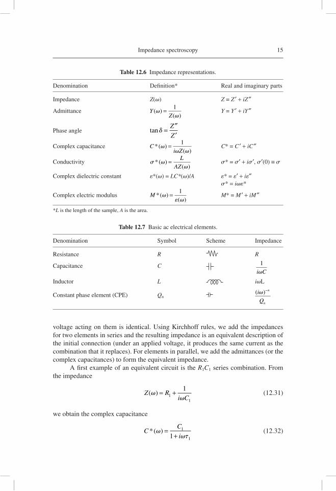
Switching the data between representations is a very useful tool of analysis in IS. The most frequently used functions are described in Table 12.6 [12.73] indicating also the separation of the magnitudes in their real and imaginary parts.
12.3.3 Simple equivalent circuits
Many measurements of IS in electrochemistry and materials devices can be described by equivalent circuits composed of combinations of a few elements that are indicated in Table 12.7. Equivalent circuits are formed by connecting these and other elements by wires, representing low resistance paths in the system. Two elements are in series when the current through them is the same, whereas they are in parallel when the
Q1Q1
Impedance spectroscopy 15
voltage acting on them is identical. Using Kirchhoff rules, we add the impedances for two elements in series and the resulting impedance is an equivalent description of the initial connection (under an applied voltage, it produces the same current as the combination that it replaces). For elements in parallel, we add the admittances (or the complex capacitances) to form the equivalent impedance.
A fi rst example of an equivalent circuit is the R1C1 series combination. From the impedance
Z R
i C( )v
v= +1
1
1 (12.31)
we obtain the complex capacitance
C
C
i*( )v
v=
+1
11 t (12.32)
Table 12.6 Impedance representations.
Denomination Defi nition* Real and imaginary parts
Impedance Z(v) Z = Z ′ + iZ″
Admittance YZ
( )( )
vv
= 1 Y = Y ′ + iY″
Phase angle tand = Z
Z
″′
Complex capacitance Ci Z
*( )( )
vv v
= 1 C* = C ′ + iC″
Conductivity s*( )( )
vv
= L
AZ s* = s′ + is′, s′(0) ≡ s
Complex dielectric constant e*(v) = LC*(v)/A e* = e′ + ie″ s* = ive*
Complex electric modulus M *( )( )
vv
= 1
e M* = M ′ + iM″
*L is the length of the sample, A is the area.
Table 12.7 Basic ac electrical elements.
Denomination Symbol Scheme Impedance
Resistance R R
Capacitance C 1
i Cv
Inductor L ivL
Constant phase element (CPE) Qn ( )i
Q
n
n
v−
16 Dye-sensitized solar cells
Here, the relaxation time is defi ned as
t = R1C1 (12.33)
Let us look more closely at the meaning of the relaxation time, t1, in relation to the response of the system in the time domain. We consider the type of measurement commented before, in which a change of voltage, ΔV, is applied at time t = 0, and for which the subsequent evolution of the electrical current is monitored. In the frequency domain, the step voltage ˆ ( ) ( )V t V u t= ⋅Δ has the expression:
ˆ ( )V s
V
s= Δ
(12.34)
and the electrical current can be written:
ˆ( )ˆ ( )
( ) ( ) ( )I s
V s
Z s
V
sZ s
V
R s= = =
+Δ Δt
t
1
1 11 (12.35)
By inverting Eq. (12.35) to the time domain, we obtain:
I t
V
Re t( ) /= −Δ t1 (10.36)
In general, the process described by Eqs. (12.32) or (12.36) is an elementary relaxation with the characteristic frequency:
v1
1 1 1
1 1= =t R C
(12.37)
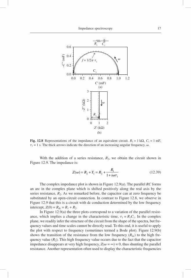
The plot of the complex capacitance is shown in Figure 12.8(a). The capaci-tance displays an arc from the dc value C*(0) = C1 to the high frequency value. The top of the arc occurs at the characteristic frequency of the relaxation v1. The impedance, shown in the complex plane in Figure 12.8(b), forms a vertical line. This is a “blocking” circuit, since the impedance of a capacitor is ∞ at low frequency, which effectively constitutes an open circuit connection, thus preventing the dc cur-rent from fl owing. However, the impedance of the capacitor decreases as the fre-quency increases, and at very large frequencies, with respect to v1, the capacitor indeed becomes a short-circuit. Consequently, there remains only the resistance R1. The impedance of a resistor is the same at all frequencies, hence the vertical line in Figure 12.8(b). The arc in Figure 12.8(a) is a manifestation of an elementary relaxa-tion process that corresponds to an exponential decay in the time domain, indicated in Eq. (12.36).
Another important example of an equivalent circuit is the RC parallel combina-tion, depicted in Figure 12.9. The admittance of the combination is here:
Y
Ri C1
11
1( )v v= + (12.38)
Impedance spectroscopy 17
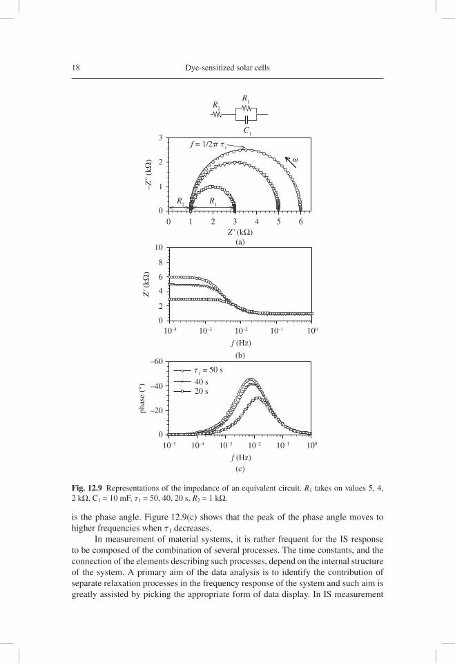
With the addition of a series resistance, R2, we obtain the circuit shown in Figure 12.9. The impedance is:
Z R Y R
R
i( )v
v= + = +
+2 1 21
11 t (12.39)
The complex impedance plot is shown in Figure 12.9(a). The parallel RC forms an arc in the complex plane which is shifted positively along the real axis by the series resistance, R2. As we remarked before, the capacitor can at zero frequency be substituted by an open-circuit connection. In contrast to Figure 12.8, we observe in Figure 12.9 that this is a circuit with dc conduction determined by the low frequency intercept, Z(0) = Rdc = R1 + R2.
In Figure 12.9(a) the three plots correspond to a variation of the parallel resist-ance, which implies a change in the characteristic time, t1 = R1C1. In the complex plane, we readily infer the structure of the circuit from the shape of the spectra, but fre-quency values and time scales cannot be directly read. To this end, it is useful to apply the plot with respect to frequency (sometimes termed a Bode plot). Figure 12.9(b) shows the transition of the resistance from the low frequency (Rdc) to the high fre-quency value (R2). This high frequency value occurs due to the fact that the capacitor impedance disappears at very high frequency, Z(v = ∞) = 0, thus shunting the parallel resistance. Another representation often used to display the characteristic frequencies
(b)
3
2
1
00 1 2
Z' (kΩ)
–Z"
(kΩ
)(a)
0.6R
1
f = 1/2p t1
v
C1
C1
0.4
0.2
0.00.0 0.2 0.4 0.6
C' (mF)
–C"
(mF)
0.8 1.0 1.2
v
R1
Fig. 12.8 Representations of the impedance of an equivalent circuit. R1 = 1 kΩ, C1 = 1 mF, t1 = 1 s. The thick arrows indicate the direction of an increasing angular frequency, v.
18 Dye-sensitized solar cells
is the phase angle. Figure 12.9(c) shows that the peak of the phase angle moves to higher frequencies when t1 decreases.
In measurement of material systems, it is rather frequent for the IS response to be composed of the combination of several processes. The time constants, and the connection of the elements describing such processes, depend on the internal structure of the system. A primary aim of the data analysis is to identify the contribution of separate relaxation processes in the frequency response of the system and such aim is greatly assisted by picking the appropriate form of data display. In IS measurement
R2
R2
R1
R1
C1
3f = 1/2p t
1
v
–Z"
(kΩ
)
Z' (kΩ)(a)
(b)
(c)
Z' (
kΩ)
phas
e (°
)
2
10
8
6
4
2
0
–60t
1 = 50 s
40 s20 s
–40
–20
0
10–4
10–5 10–4 10–3 10–2 10–1 100
10–3 10–2
f (Hz)
f (Hz)
10–1 100
1
00 1 2 3 4 5 6
Fig. 12.9 Representations of the impedance of an equivalent circuit. R1 takes on values 5, 4, 2 kΩ, C1 = 10 mF, t1 = 50, 40, 20 s, R2 = 1 kΩ.
Impedance spectroscopy 19
we obtain the data, and such data can be transformed as desired between the various representations of Table 12.6.
As mentioned in a previous section, the most critical information concerning solar cell device operation in stationary conditions relates to the separation of resist-ances. However, in IS, capacitances also play a crucial role, since different elements with similar resistance provide very distinct spectral features if their associated capac-itances differ suffi ciently in magnitude. The capacitance is, therefore, a key to the understanding of the origin of the measured resistances.
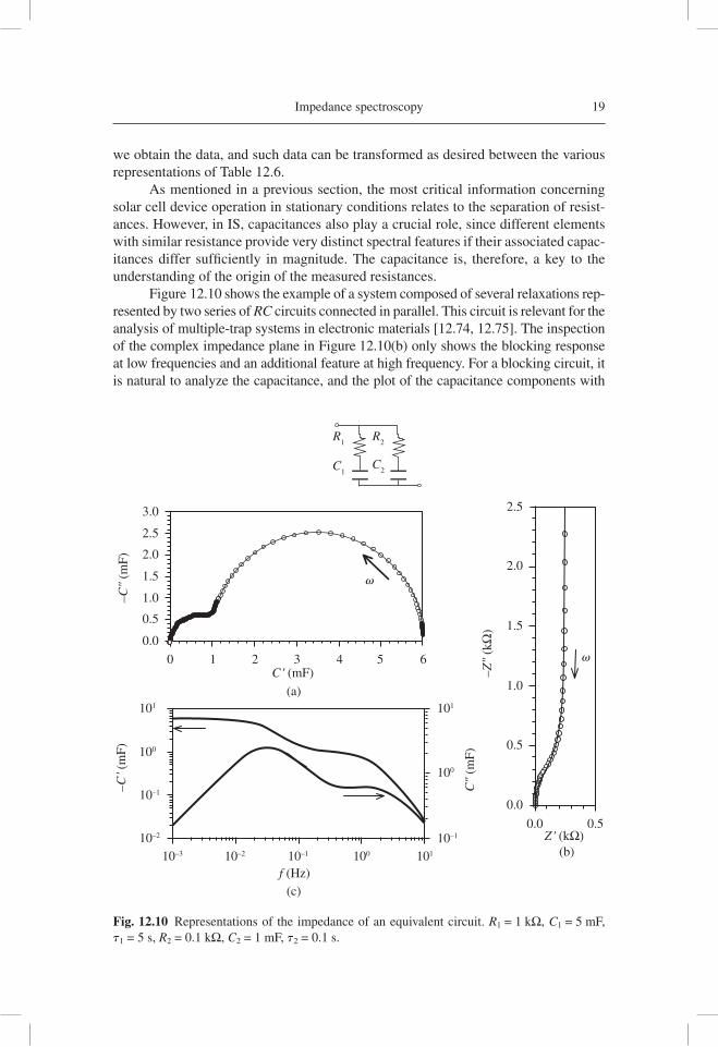
Figure 12.10 shows the example of a system composed of several relaxations rep-resented by two series of RC circuits connected in parallel. This circuit is relevant for the analysis of multiple-trap systems in electronic materials [12.74, 12.75]. The inspection of the complex impedance plane in Figure 12.10(b) only shows the blocking response at low frequencies and an additional feature at high frequency. For a blocking circuit, it is natural to analyze the capacitance, and the plot of the capacitance components with
0.0
0.5
1.0
1.5
2.0
2.5
0.0 0.5Z' (kΩ)
–Z"
(kΩ
)
10–2 10–1
f (Hz)100 101
10–1
100
C"
(mF)
–C' (
mF)
101
10–3
10–2
10–1
100
101
C' (mF)
–C"
(mF)
0 1 2 3 4 5 6
0.0
0.5
1.0
1.5
2.0
2.5
3.0
v
v
R1
C1
R2
C2
(a)
(c)
(b)
Fig. 12.10 Representations of the impedance of an equivalent circuit. R1 = 1 kΩ, C1 = 5 mF, t1 = 5 s, R2 = 0.1 kΩ, C2 = 1 mF, t2 = 0.1 s.
20 Dye-sensitized solar cells
respect to the frequency, Figure 12.10(c), usually reveals a great deal of information. In Figure 12.10(c), we observe two plateaus of the real part of the capacitance which clearly indicate two distinct relaxation processes. These relaxations are manifested in the peaks of the loss component of the capacitance, C′. When increasing the frequency, each peak of C′ indicates the occurrence of a relaxation and a consequent decrease of the capacitance [12.72]. Such features can also be observed in the complex capacitance plot in Figure 12.10(a), demonstrating separate arcs for the two relaxations.
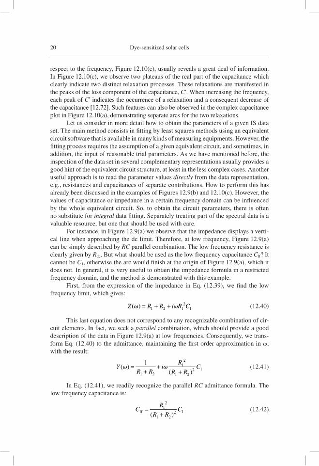
Let us consider in more detail how to obtain the parameters of a given IS data set. The main method consists in fi tting by least squares methods using an equivalent circuit software that is available in many kinds of measuring equipments. However, the fi tting process requires the assumption of a given equivalent circuit, and sometimes, in addition, the input of reasonable trial parameters. As we have mentioned before, the inspection of the data set in several complementary representations usually provides a good hint of the equivalent circuit structure, at least in the less complex cases. Another useful approach is to read the parameter values directly from the data representation, e.g., resistances and capacitances of separate contributions. How to perform this has already been discussed in the examples of Figures 12.9(b) and 12.10(c). However, the values of capacitance or impedance in a certain frequency domain can be infl uenced by the whole equivalent circuit. So, to obtain the circuit parameters, there is often no substitute for integral data fi tting. Separately treating part of the spectral data is a valuable resource, but one that should be used with care.
For instance, in Figure 12.9(a) we observe that the impedance displays a verti-cal line when approaching the dc limit. Therefore, at low frequency, Figure 12.9(a) can be simply described by RC parallel combination. The low frequency resistance is clearly given by Rdc. But what should be used as the low frequency capacitance Clf? It cannot be C1, otherwise the arc would fi nish at the origin of Figure 12.9(a), which it does not. In general, it is very useful to obtain the impedance formula in a restricted frequency domain, and the method is demonstrated with this example.
First, from the expression of the impedance in Eq. (12.39), we fi nd the low frequency limit, which gives:
Z R R i R C( )v v= + +1 2 12
1 (12.40)
This last equation does not correspond to any recognizable combination of cir-cuit elements. In fact, we seek a parallel combination, which should provide a good description of the data in Figure 12.9(a) at low frequencies. Consequently, we trans-form Eq. (12.40) to the admittance, maintaining the fi rst order approximation in v, with the result:
Y
R Ri
R
R RC( )
( )v v=
++
+1
1 2
12
1 22 1 (12.41)
In Eq. (12.41), we readily recognize the parallel RC admittance formula. The low frequency capacitance is:
C
R
R RClf =
+12
1 22 1( )
(12.42)
Impedance spectroscopy 21
The capacitance therefore depends on the resistances of the original circuit. This result is quite natural, since the capacitance relates to the reciprocal of the impedance (see Table 12.6), and the latter is greatly infl uenced by the series resistance. However, the result in Eq. (12.42) cannot be inferred without a proper calculation.
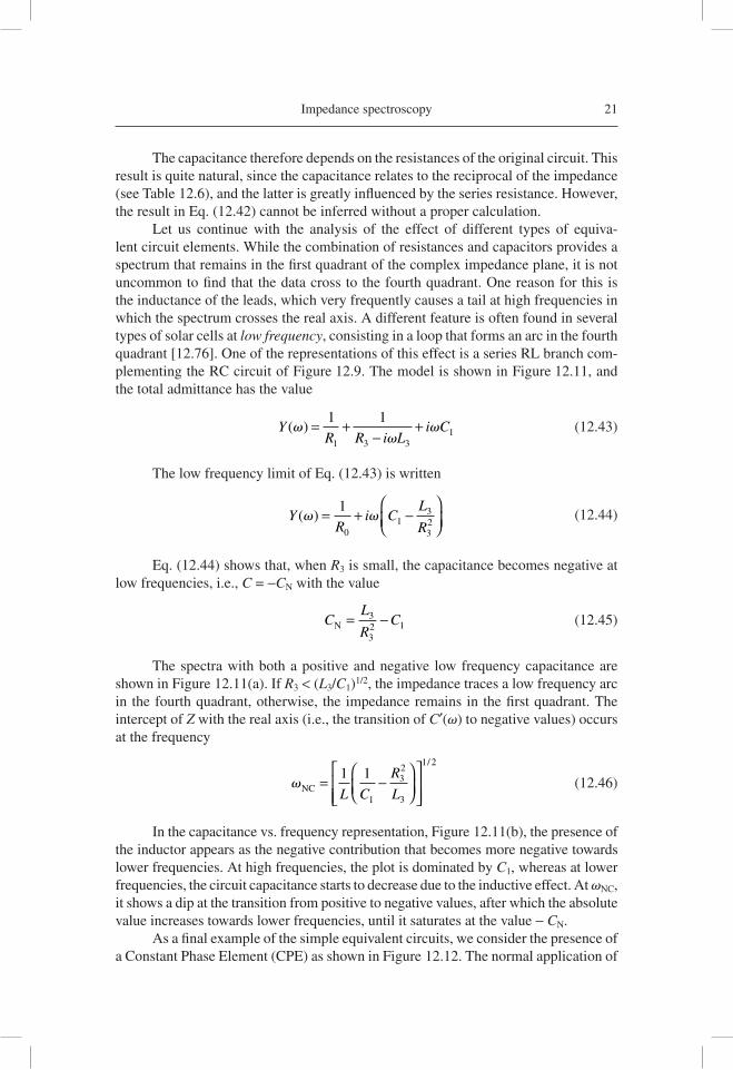
Let us continue with the analysis of the effect of different types of equiva-lent circuit elements. While the combination of resistances and capacitors provides a spectrum that remains in the fi rst quadrant of the complex impedance plane, it is not uncommon to fi nd that the data cross to the fourth quadrant. One reason for this is the inductance of the leads, which very frequently causes a tail at high frequencies in which the spectrum crosses the real axis. A different feature is often found in several types of solar cells at low frequency, consisting in a loop that forms an arc in the fourth quadrant [12.76]. One of the representations of this effect is a series RL branch com-plementing the RC circuit of Figure 12.9. The model is shown in Figure 12.11, and the total admittance has the value
Y
R R i Li C( )v
vv= +
−+1 1
1 3 31 (12.43)
The low frequency limit of Eq. (12.43) is written
YR
i CL
R( )v v= + −
⎛
⎝⎜⎞
⎠⎟1
01
3
32
(12.44)
Eq. (12.44) shows that, when R3 is small, the capacitance becomes negative at low frequencies, i.e., C = −CN with the value
C
L
RCN = −3
32 1 (12.45)
The spectra with both a positive and negative low frequency capacitance are shown in Figure 12.11(a). If R3 < (L3/C1)1/2, the impedance traces a low frequency arc in the fourth quadrant, otherwise, the impedance remains in the fi rst quadrant. The intercept of Z with the real axis (i.e., the transition of C′(v) to negative values) occurs at the frequency
vNC = −⎛
⎝⎜⎞
⎠⎟⎡
⎣⎢⎢
⎤
⎦⎥⎥
1 1
1
32
3
1 2
L C
R
L
/
(12.46)
In the capacitance vs. frequency representation, Figure 12.11(b), the presence of the inductor appears as the negative contribution that becomes more negative towards lower frequencies. At high frequencies, the plot is dominated by C1, whereas at lower frequencies, the circuit capacitance starts to decrease due to the inductive effect. At vNC, it shows a dip at the transition from positive to negative values, after which the absolute value increases towards lower frequencies, until it saturates at the value − CN.
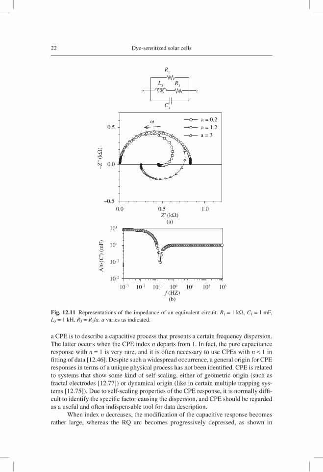
As a fi nal example of the simple equivalent circuits, we consider the presence of a Constant Phase Element (CPE) as shown in Figure 12.12. The normal application of
22 Dye-sensitized solar cells
a CPE is to describe a capacitive process that presents a certain frequency dispersion. The latter occurs when the CPE index n departs from 1. In fact, the pure capacitance response with n = 1 is very rare, and it is often necessary to use CPEs with n < 1 in fi tting of data [12.46]. Despite such a widespread occurrence, a general origin for CPE responses in terms of a unique physical process has not been identifi ed. CPE is related to systems that show some kind of self-scaling, either of geometric origin (such as fractal electrodes [12.77]) or dynamical origin (like in certain multiple trapping sys-tems [12.75]). Due to self-scaling properties of the CPE response, it is normally diffi -cult to identify the specifi c factor causing the dispersion, and CPE should be regarded as a useful and often indispensable tool for data description.
When index n decreases, the modifi cation of the capacitive response becomes rather large, whereas the RQ arc becomes progressively depressed, as shown in
10–1 100 101 102 10310–210–3
10–2
10–1
100
101
a = 0.2a = 1.2a = 3
1.00.50.0
–Z"
(kΩ
)
Z' (kΩ)(a)
(b)f (HZ)
Abs
(C')
(mF)
–0.5
0.0
0.5v
L3
R3
C1
R1
Fig. 12.11 Representations of the impedance of an equivalent circuit. R1 = 1 kΩ, C1 = 1 mF, L3 = 1 kH, R3 = R1/a, a varies as indicated.
Impedance spectroscopy 23
Figure 12.12(a). The CPE also gives rise to a signifi cant deceleration of the response. Figure 12.12(b) shows that the transition from a low to high frequency resistance of the capacitor response is completed in less than two decades of frequency, while for n = 0.6, it requires more than four decades. Consequently, the characteristic frequency presents an important reduction as n decreases, according to the expres-sion [12.46]
v1
1 11
1=
( )R Qn/
(12.47)
The foregoing discussion has shown that equivalent circuit representations are a very powerful resource for the inverse problem that is usually a main task in IS data treatment: to establish an impedance model from a set of data. Importantly, equivalent
10–5
0
1
2
n = 10.80.6
10–4
f (Hz)
Z' (
KΩ
)
10–3 10–2 10–1
1.5
1.0
0.5
0.0
0.0 0.5 1.0 1.5Z' (kΩ)
–Z"
(kΩ
)
2.0 2.5
R1
Q1
R2
(a)
(b)
v
Fig. 12.12 Representations of the impedance of an equivalent circuit. R1 = 2 kΩ, C1 = 10 mF.sn−1, n varies as indicated, and R2 = 0.1 kΩ.
24 Dye-sensitized solar cells
circuits render it possible to visualize the structure of the model and to separately treat data portions in certain relevant frequency windows. However, equivalent circuits are by no means necessary in order to establish a physical model; what is needed is an impedance function, in any of all its possible analytical representations.
It should also be mentioned, that not all complex functions of frequency are valid impedance responses. The complex function Z(v) must obey causality condi-tions (i.e., the stimulus must precede the response), which imposes analytical con-straints known as Kramers-Kronig transforms [12.72]. These transforms enable the construction of the real part of Z(v) provided that the imaginary part is known at all frequencies, and vice versa. Using equivalent circuit elements, such as those of Table 12.6, ensures that the resulting model obeys the Kramers-Kronig relations.
12.4 BASIC PHYSICAL MODEL AND PARAMETERS OF IS IN SOLAR CELLS
12.4.1 Simplest impedance model of a solar cell
In the process of obtaining physical information from IS data, it is necessary to relate the observable equivalent circuit elements with the system properties. As mentioned before, equivalent circuits are a useful tool for interpretation, and the signifi cance attached to the circuit elements, the potential in the circuit, etc., may be quite different from the standard physics textbook examples.
This is particularly the case in the analysis of solar cells. Note that the ac-equivalent circuits that we have discussed are composed of passive elements (i.e., resistances and capacitances). It is common to interpret the fl ow of charges in cir-cuits in terms of the mechanistic view of the drift of charges in an electrical fi eld caused by potential differences. This image is also very popular for explaining the photovoltaic action, e.g., in a p-n junction, in terms of an electric fi eld that sends oppositely charged carriers in different directions. However, a solar cell is a kind of battery, i.e., an element producing an electromotive force, and such an element cannot work with electrostatic voltage differences alone. According to Volta’s idea, the electromotive force is an nonelectrostatic action on charges in conductors that causes unequal charges to separate and remain separated [12.78]. We thus wish to obtain the internal ac-equivalent circuit of a solar cell using only linear elements associated to a small signal ac perturbation, with emphasis on the interpretation of the elements that make it work as a device for the production of electricity. The key approach for useful reading of ac-equivalent circuits of DSC, is that potentials in the circuit represent an electrochemical potential of electrons (or holes) in the actual device.
To clarify this, we start with the simplest model of a solar cell, discussed above in Sec. 12.2.2, which contains the necessary elements without complications of car-rier transport, specifi c features of selective contacts, etc. We calculate the IS response of the solar cell of Figure 12.4 [12.35], corresponding to the application of a small ac electrical perturbation.
Impedance spectroscopy 25
It was demonstrated before that the dynamic response of the simple solar cell model in Figure 12.4 was determined by the equation:
∂∂
= − −n
tG U
j
qLn (12.48)
where G = GΦ + Gd is the carrier generation rate. In order to calculate the IS response, we need to combine two approaches: (1) All physical quantities are composed of a stationary part (e.g., n) and a small perturbation part that varies with time. (2) We must reduce all the dependencies implicit in Eq. (12.48), explicitly to voltage, so that the result becomes an impedance.
For example, the carrier density dependence on time takes the form:
n t n n t( ) = + ( )ˆ (12.49)
The variation of voltage applied in the solar cell produces a variation of the electron Fermi level, which changes according to:
E t E q tFn Fn n( ) = + ( )w (12.50)
where wn is the small perturbation voltage. However, with by Eq. (12.15), there is a unique dependence of n on EFn. Thus:
n t n E( ) = +( )Fn nw (12.51)
Expanding Eq. (12.51) to fi rst order, we obtain:
n t n
n
E( ) = +
∂∂
c
Fnnw (12.52)
The derivative in Eq. (12.52) appears recurrently in solar cell theory and requires a special denomination. We introduce the chemical capacitance, a thermody-namic quantity that refl ects the capability of a system to accept or release additional carriers with density Ni due to a change in their chemical potential, mi [12.35, 12.79]. In general, for a volume element that stores chemical energy due to a thermodynamic displacement, the chemical capacitance per unit volume is defi ned as:
c q
Nm
m=
∂∂
2 i
i
(12.53)
More generally, Eq. (12.53) employs the electrochemical potential, that coin-cides with the electron Fermi level [12.60]. Thus, the chemical capacitance for con-duction band electrons is [12.35]:
c q
n
E
q n
k T
N q
k TE E k Tm
cb
Fn B
c
BC Fn B=
∂∂
= = − −( )⎡⎣ ⎤⎦2
2 2
exp / (12.54)
The macroscopic capacitance for a fi lm of thickness L, area A and porosity p is written as:
C LA p cm m
cb cb= −( )1 (12.55)
26 Dye-sensitized solar cells
where LA(1 − p) is the amount and Vf is the volume of the fi lm. Using Eqs. (12.49), (12.52) and (12.54), we arrive at the relationship between the small perturbation of carrier density and voltage:
ˆ ˆn
qc=
1m
cbnw (12.56)
Next, we expand the recombination term in Eq. (12.48) and obtain:
U t U
U
nn U
U
n
c
qn nn
nn
cb
n( ) = +∂∂
⎛⎝⎜
⎞⎠⎟
= +∂∂
⎛⎝⎜
⎞⎠⎟
ˆ ˆmw (12.57)
Finally, the current can be expressed as
j t j j t( ) = + ( )ˆ (12.58)
When we insert the different expanded expressions into Eq. (12.48), we fi rst obtain a time-independent equation that has already been discussed, (12.12), and which gives the stationary condition of the solar cell according to bias voltage and illumination. In addition, the time dependent terms provide a new equation that takes the form:
c
t r
j
Ln
m
cb n
rcb
∂∂
+ + =ˆ ˆ ˆw w
0 (12.59)
where the recombination resistance per unit volume is given by:
rc
U
nrcb
cbn=
∂∂
⎛⎝⎜
⎞⎠⎟
−1
1
m
(12.60)
Note that Eq. (12.60) can be represented by the following expression:
r qU
Ercb n
Fn
=∂∂
⎛⎝⎜
⎞⎠⎟
−2
1
(10.61)
and the macroscopic recombination resistance, which corresponds to the reciprocal derivative of the recombination current with respect to voltage, is written as:
R
LA prr
cbrcb=
−1
1( ) (12.62)
The fundamental parameter describing recombination, however, is the recom-bination per unit of effective internal area (Aeff) r A R LA p hR hr′r = = − =eff r r r( ) ,1 where h is the ratio between the effective area and the volume of the TiO2 fi lm, i.e., h = Aeff/LA(1 − p).
We remark that the carrier generation terms are absent from Eq. (12.59), since it is only possible to modulate electrical injection of carriers in IS; the situation is differ-ent in light-modulated techniques, as explained by Peter and Hagfeldt in Chapter 11.
Impedance spectroscopy 27
The structure of the impedance model can be inferred directly from Eq. [12.59] [12.35]. wn can be viewed as the potential in an equivalent circuit (but one should remember that it is physically the electrochemical potential!). Then, Eq. (12.59) is Kirchoff’s rule for current conservation. The fi rst term is a capacitive current, the sec-ond is an ohmic current through the resistor Rr, and the third is the extraction current. Note that the two fi rst currents do not represent transport currents (i.e., an ensemble of carriers moving in a certain direction in space), but rather the rates of creation and destruction of conduction band electrons. In fact, recombination is what maintains the current in a diode, as explained in the book by Sha [12.69].
In order to calculate the impedance, we apply the Laplace transform (∂/∂t → iv) in Eq. (12.59) and use the defi nition in Eq. (12.22):
Zj L
ri c
n= − =+
ˆˆw
v
1 11
rcb
cbm
(12.63)
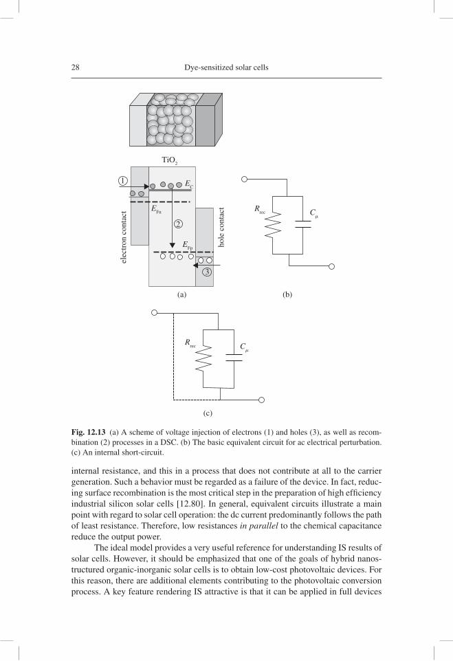
Eq. (12.63) clearly corresponds to the parallel combination of the chemical capacitance and recombination resistance, which is the minimal IS model of a solar cell. Figure 12.13(b) shows the equivalent circuit corresponding to the basic solar cell scheme of Figure 12.13(a).
In Figure 12.13(b), we can observe that the chemical capacitance is a necessary element of the solar cell: it produces a voltage (associated to a splitting of Fermi levels) by the creation of excess carriers from photons. An important message in Figure 12.13 is that the recombination resistance needs to be be large, as this will allow carri-ers accumulated in the capacitive element to fl ow through the external circuit when returning to the equilibrium situation. We point out that the recombination resistance in Figure 12.13(b) corresponds to the diode in the dc circuit of Figure 12.5.
Figure 12.13(b) also displays the special structure of connection of the R and C elements by selective contacts which is implicit in the derivation of the result in Eq. (12.63). This connection is essential in order to channel the carriers in the desired direction. An example of the failure of selective contacts is shown in Figure 12.13(c). Electrons and holes meet directly at the left contact, producing an internal short cir-cuit. Such a device cannot produce a photovoltage.
It should also be recognized that, in contrast to electrochemical batteries and capacitors, there is in solar cells always an electrical connection between the outer electrodes via the internal resistance, rr. In fact, the solar cell works by promotion of carriers from a low to a high energy level, with the energy of the photons [12.33], and such energy levels are separately connected to the outer electrodes. Since the excita-tion is possible, the converse process, which is the decay from a high to a low energy level by radiative recombination, must also be possible. This is the most favorable case of the recombination resistance, which is unavoidable, as it is an intrinsic com-ponent of the photophysical process causing the solar cell to produce useful work. In this sense, we regard Figure 12.13(b) as the minimal model.
Nevertheless, while certain recombination processes are unavoidable in the solar cell, additional sources of recombination are detrimental to the performance. For example, in Figure 12.13(c), a strong recombination at the left contact produces a low
28 Dye-sensitized solar cells
internal resistance, and this in a process that does not contribute at all to the carrier generation. Such a behavior must be regarded as a failure of the device. In fact, reduc-ing surface recombination is the most critical step in the preparation of high effi ciency industrial silicon solar cells [12.80]. In general, equivalent circuits illustrate a main point with regard to solar cell operation: the dc current predominantly follows the path of least resistance. Therefore, low resistances in parallel to the chemical capacitance reduce the output power.
The ideal model provides a very useful reference for understanding IS results of solar cells. However, it should be emphasized that one of the goals of hybrid nanos-tructured organic-inorganic solar cells is to obtain low-cost photovoltaic devices. For this reason, there are additional elements contributing to the photovoltaic conversion process. A key feature rendering IS attractive is that it can be applied in full devices
hole
con
tact
elec
tron
con
tact
EC
Rrec
Rrec
Cm
Cm
EFn
EFp
2
3
(a) (b)
(c)
1
TiO2
Fig. 12.13 (a) A scheme of voltage injection of electrons (1) and holes (3), as well as recom-bination (2) processes in a DSC. (b) The basic equivalent circuit for ac electrical perturbation. (c) An internal short-circuit.
Impedance spectroscopy 29
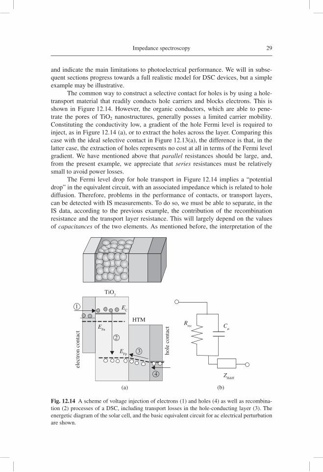
and indicate the main limitations to photoelectrical performance. We will in subse-quent sections progress towards a full realistic model for DSC devices, but a simple example may be illustrative.
The common way to construct a selective contact for holes is by using a hole-transport material that readily conducts hole carriers and blocks electrons. This is shown in Figure 12.14. However, the organic conductors, which are able to pene-trate the pores of TiO2 nanostructures, generally posses a limited carrier mobility. Constituting the conductivity low, a gradient of the hole Fermi level is required to inject, as in Figure 12.14 (a), or to extract the holes across the layer. Comparing this case with the ideal selective contact in Figure 12.13(a), the difference is that, in the latter case, the extraction of holes represents no cost at all in terms of the Fermi level gradient. We have mentioned above that parallel resistances should be large, and, from the present example, we appreciate that series resistances must be relatively small to avoid power losses.
The Fermi level drop for hole transport in Figure 12.14 implies a “potential drop” in the equivalent circuit, with an associated impedance which is related to hole diffusion. Therefore, problems in the performance of contacts, or transport layers, can be detected with IS measurements. To do so, we must be able to separate, in the IS data, according to the previous example, the contribution of the recombination resistance and the transport layer resistance. This will largely depend on the values of capacitances of the two elements. As mentioned before, the interpretation of the
hole
con
tact
elec
tron
con
tact
EC
Rrec
ZHdiff
CmE
Fn
EFp
2
3
HTM
4
(a) (b)
1
TiO2
Fig. 12.14 A scheme of voltage injection of electrons (1) and holes (4) as well as recombina-tion (2) processes of a DSC, including transport losses in the hole-conducting layer (3). The energetic diagram of the solar cell, and the basic equivalent circuit for ac electrical perturbation are shown.
30 Dye-sensitized solar cells
capacitance is a major tool for identifying the physical origin of processes observed in IS measurements.
12.4.2 Measurements of electron lifetimes
It is interesting to explain in more detail the relationship between the equivalent circuit elements describing the solar cell IS response and the electron lifetime. In order to describe the IS behavior, we have considered in Eq. (12.63) an experiment relating voltage to an electrical current measurement. However, we can employ the general dynamic equation (12.59) in experiments in which we apply a perturbation and let the system decay by itself [12.54, 12.57]. Since no current is extracted, we obtain:
∂∂
= − =ˆ ˆ ˆw w wn n
rcb cb
n
rcb cbt r c R Cm m
(12.64)
Eq. (12.64) describes, for instance, the exponential decay of a small step of excess carrier concentration by recombination. From Eq. (12.64), the time constant of the decay process, which we denote the response time, is:
t mr r
cb cb= r c (12.65)
In the model outlined above, this also gives:
tr = ∂
∂⎛⎝⎜
⎞⎠⎟
−U
n
1
(12.66)
With the normal assumption of a fi rst-order reaction for direct electron trans-fer from the conduction band, Eq. (12.5), we obtain simply tr = t0. In this simple model, the lifetime is constant, and the response time and electron lifetime have the same meaning. But in general, the lifetime can be dependant on steady-state conditions, as is obvious in Eq. (12.66). In addition, in the presence of additional relaxation processes such as trapping and release in localized electronic states, the response time contains components due to kinetic delays in addition to the free car-rier lifetime [12.40].
12.5 BASIC PHYSICAL MODELS AND PARAMETERS OF IS IN DYE-SENSITIZED SOLAR CELLS
12.5.1 Electronic processes in a DSC
A general view of the electronic and ionic processes occurring in a DSC is given in Figure 12.15. With respect to the basic solar cell model in Figure 12.4, the sensitizer in a DSC (molecular dye, inorganic quantum dot, etc.) is the absorber [12.33]. The selective contacts to the absorber are formed, fi rst, by an electron transport material
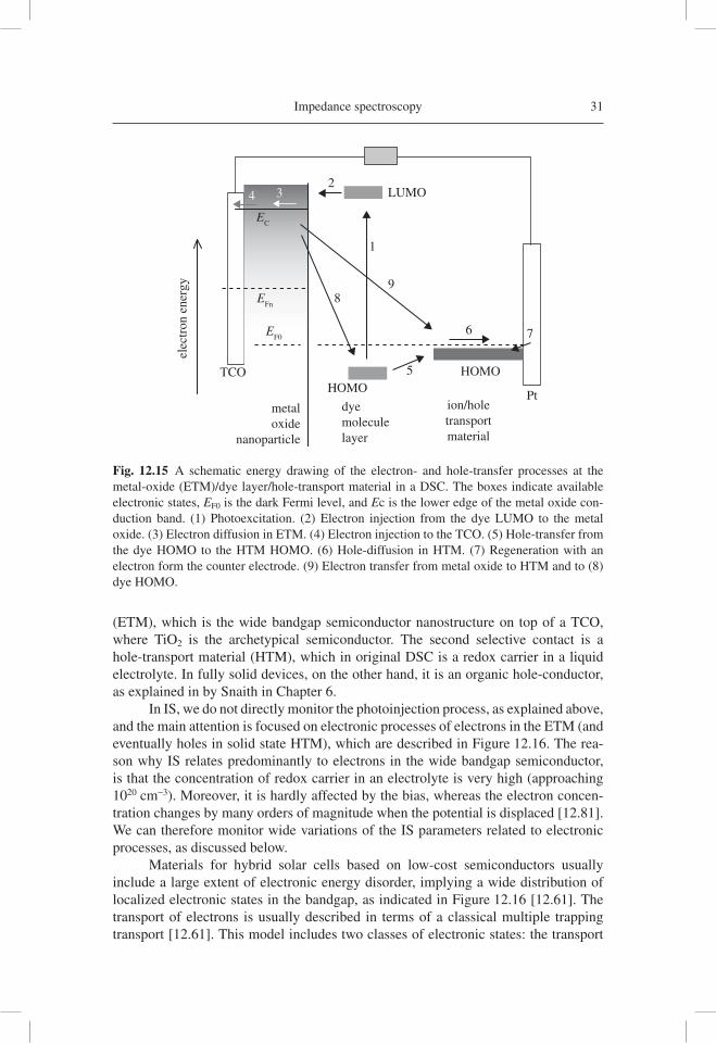
Impedance spectroscopy 31
(ETM), which is the wide bandgap semiconductor nanostructure on top of a TCO, where TiO2 is the archetypical semiconductor. The second selective contact is a hole-transport material (HTM), which in original DSC is a redox carrier in a liquid electrolyte. In fully solid devices, on the other hand, it is an organic hole-conductor, as explained in by Snaith in Chapter 6.
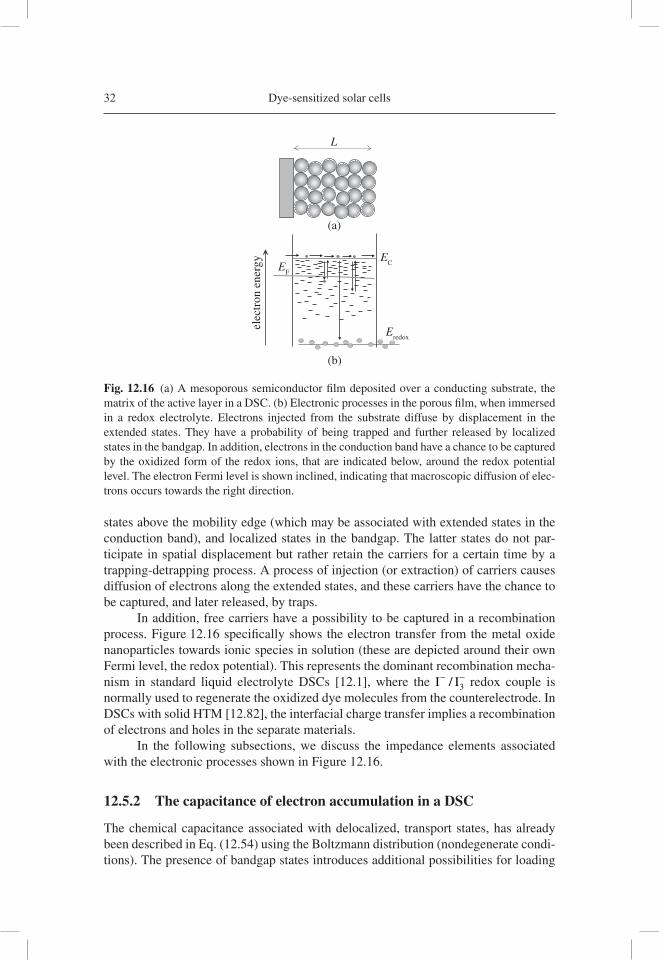
In IS, we do not directly monitor the photoinjection process, as explained above, and the main attention is focused on electronic processes of electrons in the ETM (and eventually holes in solid state HTM), which are described in Figure 12.16. The rea-son why IS relates predominantly to electrons in the wide bandgap semiconductor, is that the concentration of redox carrier in an electrolyte is very high (approaching 1020 cm−3). Moreover, it is hardly affected by the bias, whereas the electron concen-tration changes by many orders of magnitude when the potential is displaced [12.81]. We can therefore monitor wide variations of the IS parameters related to electronic processes, as discussed below.
Materials for hybrid solar cells based on low-cost semiconductors usually include a large extent of electronic energy disorder, implying a wide distribution of localized electronic states in the bandgap, as indicated in Figure 12.16 [12.61]. The transport of electrons is usually described in terms of a classical multiple trapping transport [12.61]. This model includes two classes of electronic states: the transport
TCO
elec
tron
ene
rgy
LUMO
HOMOHOMO
ion/holetransportmaterial
5
6
9
1
8
234
EC
EFn
EF0 7
Ptdyemoleculelayer
metaloxide
nanoparticle
Fig. 12.15 A schematic energy drawing of the electron- and hole-transfer processes at the metal-oxide (ETM)/dye layer/hole-transport material in a DSC. The boxes indicate available electronic states, EF0 is the dark Fermi level, and Ec is the lower edge of the metal oxide con-duction band. (1) Photoexcitation. (2) Electron injection from the dye LUMO to the metal oxide. (3) Electron diffusion in ETM. (4) Electron injection to the TCO. (5) Hole-transfer from the dye HOMO to the HTM HOMO. (6) Hole-diffusion in HTM. (7) Regeneration with an electron form the counter electrode. (9) Electron transfer from metal oxide to HTM and to (8) dye HOMO.
32 Dye-sensitized solar cells
states above the mobility edge (which may be associated with extended states in the conduction band), and localized states in the bandgap. The latter states do not par-ticipate in spatial displacement but rather retain the carriers for a certain time by a trapping-detrapping process. A process of injection (or extraction) of carriers causes diffusion of electrons along the extended states, and these carriers have the chance to be captured, and later released, by traps.
In addition, free carriers have a possibility to be captured in a recombination process. Figure 12.16 specifi cally shows the electron transfer from the metal oxide nanoparticles towards ionic species in solution (these are depicted around their own Fermi level, the redox potential). This represents the dominant recombination mecha-nism in standard liquid electrolyte DSCs [12.1], where the I I− −/ 3 redox couple is normally used to regenerate the oxidized dye molecules from the counterelectrode. In DSCs with solid HTM [12.82], the interfacial charge transfer implies a recombination of electrons and holes in the separate materials.
In the following subsections, we discuss the impedance elements associated with the electronic processes shown in Figure 12.16.
12.5.2 The capacitance of electron accumulation in a DSC
The chemical capacitance associated with delocalized, transport states, has already been described in Eq. (12.54) using the Boltzmann distribution (nondegenerate condi-tions). The presence of bandgap states introduces additional possibilities for loading
Eredox
ECE
F
elec
tron
ene
rgy
L
(a)
(b)
Fig. 12.16 (a) A mesoporous semiconductor fi lm deposited over a conducting substrate, the matrix of the active layer in a DSC. (b) Electronic processes in the porous fi lm, when immersed in a redox electrolyte. Electrons injected from the substrate diffuse by displacement in the extended states. They have a probability of being trapped and further released by localized states in the bandgap. In addition, electrons in the conduction band have a chance to be captured by the oxidized form of the redox ions, that are indicated below, around the redox potential level. The electron Fermi level is shown inclined, indicating that macroscopic diffusion of elec-trons occurs towards the right direction.
Impedance spectroscopy 33
the semiconductor with charges. For one specifi c electronic state characterized by an energy E (an energy defi ned to be increasingly negative for states deeper in the gap), the average equilibrium occupancy is determined by the Fermi level as described by the Fermi-Dirac distribution function:
f E EE E k T
( )exp /
− =+ −( )⎡⎣ ⎤⎦
FnFn B
1
1 (12.67)
If the distribution of localized states is g(E), the chemical capacitance is obtained by integrating all the contributions through the bandgap
c q g Edf
dEdEm
traps
Fn
=−∞
+∞
∫2 ( ) (12.68)
Using df (E − EFn)/dEFn = −df (E − EFn)/dE and integrating Eq. (12.68) by parts, we arrive at
c qdg
dEf E E dEm
trapsFn= −
−∞
+∞
∫2 ( ) (12.69)
A simple solution to Eq. (12.69) is obtained by the zero-temperature limit of the Fermi function, i.e., a step function at E = EFn separating occupied states from their unoccupied counterparts. It then follows that:
c q
dg
dEdE q g Em
trapsFn
Fn
= =−∞∫2 2
E
( ) (12.70)
In this approximation, Eq. (12.70), the charging related to the perturbation dV corresponds to fi lling a slice of traps at the Fermi level, as explained in Figure 12.17, and the chemical capacitance is proportional to the density of states (DOS).
A common fi nding in nanostructured TiO2 is an exponential distribution of localized states in the bandgap as described by the following expression:
g E
N
k TE E k T( ) exp ( ) /= −[ ]L
BC B
00 (12.71)
Here, NL is the total density and T0 is a parameter with temperature units deter-mining the depth of the distribution, and which can be alternatively expressed as a coeffi cient a = T/T0. According to Eqs. (12.70) and (12.71), the chemical capacitance should display an exponential dependence on the applied potential:
c
N q
k TE E k Tm
traps L
BC B= −[ ]
2
00exp ( ) / (12.72)
where the slope is q/KBT0 in log-linear representation with respect to the voltage; a fact that has been observed many times in the literature when using IS (as discussed in the next section) and cyclic voltammetry (CV) [12.51, 12.53, 12.83, 12.84]. In
34 Dye-sensitized solar cells
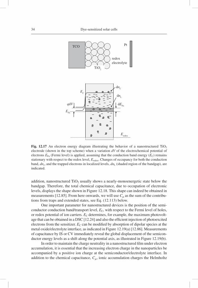
addition, nanostructured TiO2 usually shows a nearly-monoenergetic state below the bandgap. Therefore, the total chemical capacitance, due to occupation of electronic levels, displays the shape shown in Figure 12.18. This shape can indeed be obtained in measurements [12.85]. From here onwards, we will use Cm as the sum of the contribu-tions from traps and extended states, see Eq. (12.113) below.
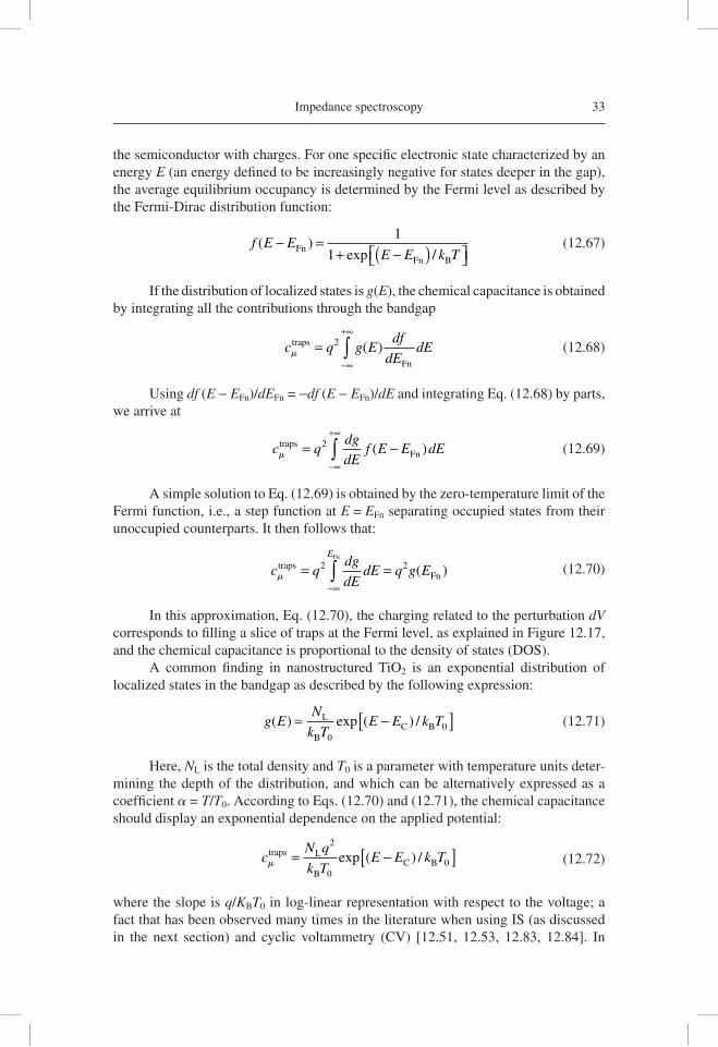
One important parameter for nanostructured devices is the position of the semi-conductor conduction band/transport level, EC, with respect to the Fermi level of holes, or redox potential of ion carriers. EC determines, for example, the maximum photovolt-age that can be obtained in a DSC [12.24] and also the effi cient injection of photoexcited electrons from the sensitizer. EC can be modifi ed by absorption of dipolar species at the metal oxide/electrolyte interface, as indicated in Figure 12.19(a) [12.86]. Measurements of capacitance by IS or CV immediately reveal the global displacement of the semicon-ductor energy levels as a shift along the potential axis, as illustrated in Figure 12.19(b).
In order to maintain the charge neutrality in a nanostructured fi lm under electron accumulation, it is essential that the increasing electron charge in the nanoparticles be accompanied by a positive ion charge at the semiconductor/electrolyte interface. In addition to the chemical capacitance, Cm, ionic accumulation charges the Helmholtz
TiO2
EC
Eredox
EFn
qdV
dnC
dnL
dEFn
TCO Pt
redoxelectrolyte
Fig. 12.17 An electron energy diagram illustrating the behavior of a nanostructured TiO2 electrode (shown in the top scheme) when a variation dV of the electrochemical potential of electrons EFn (Fermi level) is applied, assuming that the conduction band energy (EC) remains stationary with respect to the redox level, Eredox. Changes of occupancy for both the conduction band, dnc, and the trapped electrons in localized levels, dnL (shaded region of the bandgap), are indicated.
Impedance spectroscopy 35
capacitance, CH, which is usually a constant, and is connected in series. The total capacitance thus becomes:
C C C= +( )− − −
m
1 1 1
H (12.73)
Eq. (12.73) also describes the distribution of the applied bias, either as a Fermi level in the semiconductor, or as an interfacial potential drop. As discussed later in more detail, it is common for the capacitance to saturate towards CH at strong forward bias, implying that the increasing potential modifi es the voltage in the Helmholtz layer, causing the band to shift.
It should be emphasized that Cm generally depends on the properties of the electrochemical potential of the carriers. The model explained above in terms of the distribution of electronic states is one possible approach that has been found to be very useful in the interpretation of capacitance measurements of DSC [12.53, 12.87]. In general, however, ionic effects, interactions, etc., governing the electrochemical potential [12.88], will affect the chemical capacitance.
12.5.3 Recombination resistance
In the Applications Section, we demonstrate that the DSC operation is very similar to the ideal photovoltaic model that has been outlined above. The main reasons for this are that:
(1) The TCO/TiO2 contact and nanostructured TiO2 network provide a very good electron selective contact, whereby the Fermi level of the TCO follows the increase of the electron Fermi level in TiO2 nanoparticles.
(2) Electron transport is fast enough to provide long diffusion lengths.
0.0E
C
Em
–0.1
–0.2
–0.3
–0.4
–0.5
–0.60.00
Chemical capacitance (F/cm2)
Ele
ctro
n en
ergy
(eV
)
0.05 0.10 0.15
Fig. 12.18 Representation of the chemical capacitance of an exponential distribution of states with density Nexp = 1020 cm−3 below the lower edge of the conduction band (EC = 0eV) and a monoenergetic energy level with density Nm = 1018 cm−3 (Em = −0.4cV) at a temperature T = 300 K. Electrode with a 10-mm thickness.
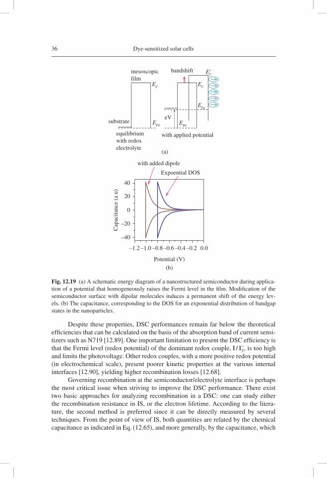
36 Dye-sensitized solar cells
Despite these properties, DSC performances remain far below the theoretical effi ciencies that can be calculated on the basis of the absorption band of current sensi-tizers such as N719 [12.89]. One important limitation to present the DSC effi ciency is that the Fermi level (redox potential) of the dominant redox couple, I I/ 3
−, is too high and limits the photovoltage. Other redox couples, with a more positive redox potential (in electrochemical scale), present poorer kinetic properties at the various internal interfaces [12.90], yielding higher recombination losses [12.68].
Governing recombination at the semiconductor/electrolyte interface is perhaps the most critical issue when striving to improve the DSC performance. There exist two basic approaches for analyzing recombination in a DSC: one can study either the recombination resistance in IS, or the electron lifetime. According to the litera-ture, the second method is preferred since it can be directly measured by several techniques. From the point of view of IS, both quantities are related by the chemical capacitance as indicated in Eq. (12.65), and more generally, by the capacitance, which
mesoscopicfilm
bandshift
EC
EC
E'C
EF0 E
F0
EFn
substrateeV
equilibriumwith redoxelectrolyte
with applied potential
(a)
(b)
with added dipole
40
20
0
–20
–40
–1.2 –1.0 –0.8 –0.6
Potential (V)
Cap
acita
nce
(a u
)
–0.4 –0.2 0.0
Expoential DOS
Fig. 12.19 (a) A schematic energy diagram of a nanostructured semiconductor during applica-tion of a potential that homogeneously raises the Fermi level in the fi lm. Modifi cation of the semiconductor surface with dipolar molecules induces a permanent shift of the energy lev-els. (b) The capacitance, corresponding to the DOS for an exponential distribution of bandgap states in the nanoparticles.
Impedance spectroscopy 37
may or may not be chemical in origin [12.91]. However, the lifetime is a quantity that corresponds to the transient behavior of the solar cell, while the recombination resistance contains primary information regarding the recombination rate at steady state [12.40]. We consider that this resistance, appearing in the fundamental circuit of Figure 12.13, is the central quantity when discussing recombination in relation to the steady state performance of DSCs. Even if we choose to study electron lifetimes, the main information on charge transfer in the lifetime is the resistance, and not the capacitance in Eq. (12.65).
Let us specify the meaning of recombination fl ux. Figure 12.4 showed that solar cell operation under illumination consists basically in the competition between two currents: the photocurrent due to extraction of the photogenerated carriers, and the recombination current which travels in the opposite sense as opposed to genera-tion. In Eq. (12.12), the recombination current was therefore jrec = qLUn. However, in practice, the situation is much more complicated, both in terms of morphology and kinetics, and we need to identify the main components of recombination through measurement. We have already mentioned the diffi culty of separating the components of a measured dc current, which is why we adopt the analysis of IS.
As discussed with regard to Eq. (12.61), we can calculate the macroscopic recombination resistance as the derivative:
R Aj
VAq
j
Errec rec
Fn
=∂∂
⎛⎝⎜
⎞⎠⎟
=∂∂
⎛⎝⎜
⎞⎠⎟
− −1 1
(12.74)
In Figure 12.15, we indicated that the recombination process in a DSC is the interfacial charge transfer of electrons in the ETM, to oxidized ions in the electrolyte or holes in the HTM. In order to perform model calculations, precise assumptions on the recombination current dependence, both with regard to the electron density and the concentration of electron acceptors in solution, or in HTM, c, are required. A simple way of formulating the recombination rate is a fi rst-order reaction, as in Eq. (12.5):
Urec = kreccn (12.75)
The recombination current density is then:
jrec = qLUrec = qLkreccn (12.76)
and we obtain from Eq. (12.74):
R
ALq k c
k Tnr
rec
B
( ) =−12
, (12.77)
If we assume that electron recombination occurs from the conduction band energy level, this last equation can also be expressed as:
R RqV
k Trcb
r= −⎡
⎣⎢
⎤
⎦⎥, exp0
B
(12.78)
38 Dye-sensitized solar cells
Eq. (12.78) shows that the recombination resistance decreases as the applied forward bias increases, due to the increasing electron density that augments the recombination rate.
In the experimental results of measurements in DSC, it is common to fi nd an expression such as Eq. (12.78), however with a different exponent, that can be param-eterized with a constant b:
R Rq V
k TrB
= −⎡
⎣⎢
⎤
⎦⎥′0 exp
b (12.79)
We should note that Eq. (12.79) is an empirical approximation that works well in restricted domains of bias voltage. The observed dependence of recombination resistance on bias may contain additional features, such as a valley, i.e., a minimum of resistance, at low potential [12.92], see Figure 12.38 below.
The parameter b in Eq. (12.79) has different denominations: it can be related to a classical electrochemical behavior known as the Tafel law, and can also be asso-ciated with the nonideality factor of the classic solar cell theory, i.e., b = 1/m in Eq. (12.1). It should nevertheless be recognized that the Tafel law in electrochemistry usually corresponds to the voltage dependence of the charge transfer rate at the metal/solution interface. In contrast, in Eq. (12.79), V is not an overpotential, but rather the Fermi level of electrons. Thus, the primary cause for the recombination resistance dependence on bias voltage in a DSC is the increase of the electron density in the inor-ganic semiconductor, as already mentioned. These two causes for the exponential law are widely recognized in photoelectrochemistry of semiconductor electrodes [12.93]. Eq. (12.78) expresses such a model in the case of ideal statistics for electrons. Eq. (12.79) corresponds to the fact that a recombination current is not simply proportional to the total electron density. As stated, such deviations are common in many classes of solar cells, even in highly effi cient silicon ones [12.94], where the diode ideality factor often departs from 1 [12.95].
Recombination in DSC depends on a multitude of factors, and these are not easy to separate in experiments using working DSC devices. While no well estab-lished consensus has been achieved regarding a fundamental quantitative description of recombination, we can provide a basic classifi cation of the main elements deter-mining recombination in the following way. Recombination is an interfacial charge transfer event at the surface between the semiconductor and the ionic/hole carrier. (Additionally, recombination from the substrate becomes important in certain circum-stances [12.96], a subject that is also treated in the Applications Section). Since the distance for electron tunneling should be on the order of 1 nm, the recombination fl ux can be naturally separated into three elements:
(1) electrons reaching recombination sites in the semiconductor surface;
(2) ions or holes reaching the surface from the electrolyte or hole-conductor side; and
(3) interfacial events.
Impedance spectroscopy 39
The electronic density in semiconductor nanoparticles in a DSC can be read-ily varied by potentiostatic control, and is accessible by several means. We can for instance obtain separate information on this by determining the chemical capacitance and transport resistance, which can be utilized as an input in the analysis of the recom-bination resistance. However, due to spatial and energetic disorder in the semicon-ductor, there are several electronic paths for charge transfer at the surface, which complicates the analysis, as further discussed below.
In contrast, as mentioned previously, for redox ionic species in the electrolyte, the concentration is very high and cannot be varied in situ, maintaining the integrity of the solar cell. For a majority of studies, the standard iodine/iodide has been employed as a redox carrier. The overall recombination reaction is given by:
I 2e (TiO ) 3I3 2− − −+ → (12.80)
The reaction (12.80) must be constituted of a multiple-step mechanism, very probably involving the species I2 [12.97], and one of the steps will be rate- determining. The oxidized species in the electrolyte may therefore be I2, and/or I3
−. Another very important issue for DSC operation is the regeneration of the oxidized dye, and this may involve a transient (dye+-iodide) intermediate complex [12.98], though such a process is diffi cult to access by IS.
The formulation of charge transfer models requires that the probability of elec-tron transfer from an electronic state at the energy level E to an acceptor species in the electrolyte with concentration c be specifi ed. This is usually given [12.99, 12.100] by the expression of the Marcus model:
νelB
B
redox
B
( ) expE kck T
k T
E E
k T= −
− −( )⎡
⎣⎢⎢
⎤
⎦⎥⎥0
22
4 4pl
l
l (12.81)
where k0 is a time constant for tunneling, which is dependent on the distance of the acceptor to the surface [12.101], and l is the reorganization energy.
It is well established that recombination rates are mainly affected by two fac-tors: (1) the position of the semiconductor energy levels, with respect to the redox levels, and (2) treatments of the surface which intercept charge transfer from the semiconductor without decreasing the rate of photoinjection from excited dye mol-ecules [12.84]. Recombination with oxidized dye molecules is thought to be of minor relevance. However, as already mentioned, while a quantitative control of electron density is possible, the measured lifetime or recombination resistance still contains a combination of mechanisms that have not been ascertained in detail.
Leaving aside the complexity of individual charge transfer events, we discuss the density dependence of the recombination resistance analyzing the various electronic paths that may occur in the semiconductor surface of a DSC. Figure 12.20(a) provides a possible outline of electronic states that participate in electron transfer at the surface [12.54, 12.102, 12.103]. Consistent with the density of states that is measured by capac-itance techniques, as indicated in Figure 12.18, we assume that the surface may contain transfer states that we classify in three kinds: the transport (conduction band) states, an exponential distribution of surface states, and a monoenergetic deep surface state.

40 Dye-sensitized solar cells
AE
C
EFn
EF0
TiO2
Eredox
Eredox
Eox
Ess
EC
EF0
Ure
Utr
Un
ss
Un
cb
l
C
B
F
D
DOS
(a)
(b)
semiconductornanoparticle
log Dredox system
elec
tron
ene
rgy
elec
tron
ene
rgy
Fig. 12.20 (a) A schematic representation of the steps involved in the recombination between the electrons in TiO2 nanoparticles and the oxidized species in the electrolyte. (EFo) shows the position of the Fermi level in the dark, equilibrated with the redox potential (Eredox) of the accep-tor species in solution. (EFn) is the Fermi level of electrons under illumination and Ec is the transport level (conduction band) energy. The following steps are indicated: (A) electron trans-port; (B) capture by surface states; electron transfer through (C) the conduction band, (D) deep mono-energetic and (F) exponential distribution of surface states. On the left side, we show the density of electronic states in the TiO2 nanoparticles, and to the right, the fl uctuating energy lev-els of oxidized species in solution according to the Marcus-Gerischer model are presented. (b) A scheme of the processes of interfacial charge transfer, displaying the electron exchange between the transport levels, and a surface state in the bandgap at energy Ess, with rates Utr and Ure for trapping and release. The rate of interfacial charge transfer from transport states is Un
cb and the rate of charge transfer from the surface state is Un
ss. l corresponds to the reorganization energy of the acceptor species in the ionic or hole transport material, with an effective density of states D. Eox is the most probable energy levels for the oxidized state of the acceptor species.
Impedance spectroscopy 41
In Figure 12.20(a), we appreciate that only transport states establish the elec-tronic communication of the surface with the substrate. So in this model, there is a single channel for transport. But when the electrons arrive at the surface, the recom-bination current branches into several parallel channels. Figure 12.20(b) provides a clearer image of the situation, by indicating in more detail the trapping and release events on a single surface state, that subsequently acts as a recombination center [12.28, 12.92].
It is now clear that, in the situation of Figure 12.20(b), the recombination cur-rent is no longer linearly dependant on the concentration of electrons in the transport state, ncb, but rather also depends on the density at the surface state, nss. In steady state, nss depends uniquely on ncb, although this dependence may be quite involved [12.102, 12.103]. In any case, in the presence of two channels for charge transfer, the recombination rate is:
U U Un ncb
nss= + (12.82)
From the general form of the recombination resistance (per unit volume) in Eq. (12.61), we may write the reciprocal resistance as:
r qU
E
U
E
q
k T
n U
rncb
Fn
nss
Fn
B
cb
cb
ns
− =∂∂
+∂∂
⎛
⎝⎜⎞
⎠⎟
= +∂
1 2
2
t
ss
Fn∂⎛
⎝⎜⎞
⎠⎟E
(12.83)
Here, tcb is the lifetime of conduction band electrons. The fi rst term in paren-theses in Eq. (12.83) recovers Eq. (12.78), while the second term introduces a differ-ent dependence.
Eq. (12.83) demonstrates nicely that the various recombination branches imme-diately translate into parallel branches in the equivalent circuit for recombination. In order to obtain a detailed understanding of recombination mechanisms in DSCs, it is of critical importance to separately measure the different recombination paths, and one may ask oneself if this is possible using IS?
The answer to this question depends on the dynamic response of the various recombination channels; i.e., whether the different channel have associated different capacitances? This would provide spectral features for discriminating the channels in the IS data.
In general, surface states, have a separate capacitive component. This is related to the chemical capacitance of each state, which is observable depending on rates of trapping and release. These are shown in Figure 12.20(b), and determine the trap resist-ance [12.75]. Indeed, in the literature of photoelectrochemistry, one may fi nd a detailed treatment of the dynamic effects of surface states [12.13, 12.14, 12.104, 12.105], and the equivalent circuit resulting from this approach is shown in Figure 12.21. Note, in particular, the resistances of the two recombination branches r rr
cbrss, , corresponding to
the two terms in Eq. (12.83). However, the dynamic effect of surface states in TiO2-based DSCs has so far not been clearly identifi ed in experiments of IS. We therefore
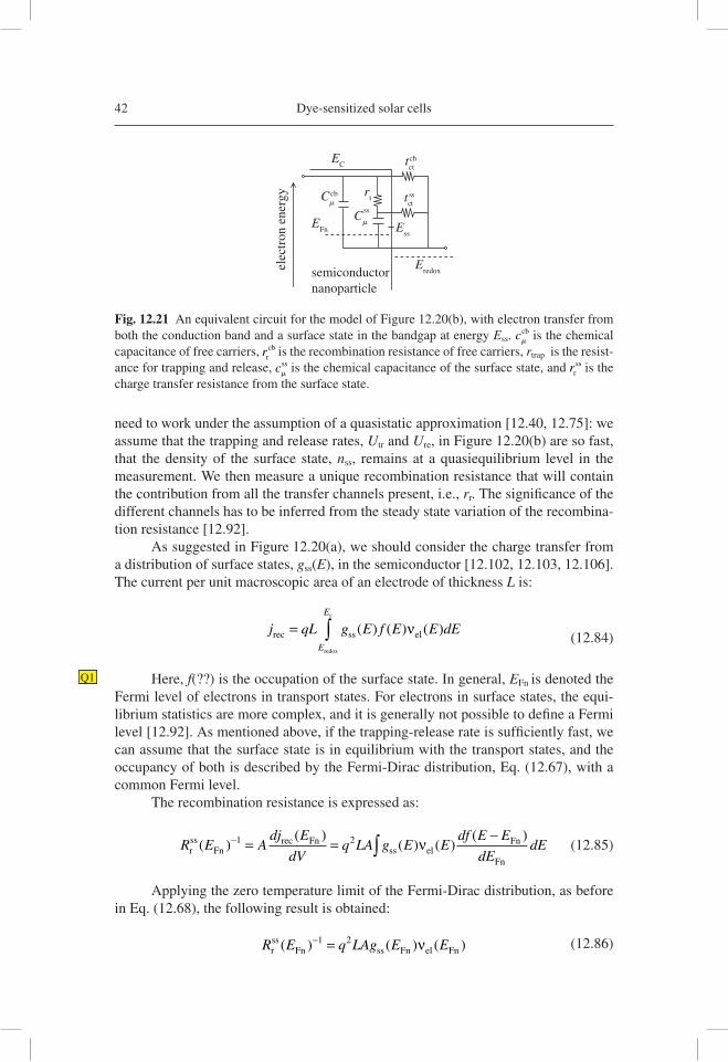
42 Dye-sensitized solar cells
need to work under the assumption of a quasistatic approximation [12.40, 12.75]: we assume that the trapping and release rates, Utr and Ure, in Figure 12.20(b) are so fast, that the density of the surface state, nss, remains at a quasiequilibrium level in the measurement. We then measure a unique recombination resistance that will contain the contribution from all the transfer channels present, i.e., rr. The signifi cance of the different channels has to be inferred from the steady state variation of the recombina-tion resistance [12.92].
As suggested in Figure 12.20(a), we should consider the charge transfer from a distribution of surface states, gss(E), in the semiconductor [12.102, 12.103, 12.106]. The current per unit macroscopic area of an electrode of thickness L is:
j qL g E f E E dEE
E
rec ss el
redox
c
= ∫ ( ) ( ) ( )ν (12.84)
Here, f(??) is the occupation of the surface state. In general, EFn is denoted the Fermi level of electrons in transport states. For electrons in surface states, the equi-librium statistics are more complex, and it is generally not possible to defi ne a Fermi level [12.92]. As mentioned above, if the trapping-release rate is suffi ciently fast, we can assume that the surface state is in equilibrium with the transport states, and the occupancy of both is described by the Fermi-Dirac distribution, Eq. (12.67), with a common Fermi level.
The recombination resistance is expressed as:
R E A
dj E
dVq LA g E E
df E E
dEdEr
ssFn
rec Fnss el
Fn
Fn
( )( )
( ) ( )( )− = =
−∫1 2 ν (12.85)
Applying the zero temperature limit of the Fermi-Dirac distribution, as before in Eq. (12.68), the following result is obtained:
R E q LAg E Erss
Fn ss Fn el Fn( ) ( ) ( )− =1 2 ν (12.86)
Q1Q1
semiconductornanoparticle
Eredox
Ess
tcsts
tcctb
EFn
EC
rt
Cm
ss
Cmcb
elec
tron
ene
rgy
Fig. 12.21 An equivalent circuit for the model of Figure 12.20(b), with electron transfer from both the conduction band and a surface state in the bandgap at energy Ess. cm
cb is the chemical capacitance of free carriers, rr
cb is the recombination resistance of free carriers, rtrap is the resist-ance for trapping and release, c
m
ss is the chemical capacitance of the surface state, and rrss is the
charge transfer resistance from the surface state.
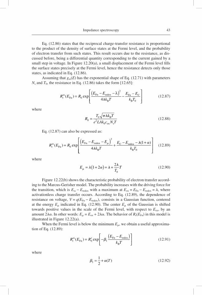
Impedance spectroscopy 43
Eq. (12.86) states that the reciprocal charge-transfer resistance is proportional to the product of the density of surface states at the Fermi level, and the probability of electron transfer from such states. This result occurs due to the resistance, as dis-cussed before, being a differential quantity corresponding to the current gained by a small step in voltage. In Figure 12.20(a), a small displacement of the Fermi level fi lls the surface states precisely at the Fermi level, hence the resistance detects only those states, as indicated in Eq. (12.86).
Assuming that gss(E) has the exponential shape of Eq. (12.71) with parameters Ns and T0, the resistance in Eq. (12.86) takes the form [12.65]:
R E RE E
k T
E E
k Trss
FnFn redox
B
Fn C
B
( ) exp=− −( )
−−⎡
⎣⎢⎢
⎤
⎦⎥⎥0
2
04
λl
(12.87)
where
R
T k T
e LAk c N T00
20
=pl B
ox s
(12.88)
Eq. (12.87) can also be expressed as:
R E RE E E
k T
E E
k Trss
FnFn redox
B
C redox
B
( ) exp( )
=− −( )
+− − +⎡
0
2
04
1m
l
l a
⎣⎣
⎢⎢
⎤
⎦
⎥⎥ (12.89)
where
E
TTm l a ll= +( ) = +1 2
2
0
(12.90)
Figure 12.22(b) shows the characteristic probability of electron transfer accord-ing to the Marcus-Gerisher model. The probability increases with the driving force for the transition, which is Ess − Eredox with a maximum at Eox = EFn − Eredox = l, where activationless charge transfer occurs. According to Eq. (12.89), the dependence of resistance on voltage, V = q(EFn − Eredox), consists in a Gaussian function, centered at the energy Em indicated in Eq. (12.90). The center Em of the Gaussian is shifted towards positive values in the scale of the Fermi level, with respect to Eox, by an amount 2la. In other words: Em = Eox + 2la. The behavior of Rr(EFn) in this model is illustrated in Figure 12.22(a).
When the Fermi level is below the minimum Em, we obtain a useful approxima-tion of Eq. (12.89):
R EE E
k Trss
FnFn redox
B
( ) exp= −−( )⎡
⎣⎢
⎤
⎦⎥R′0 b1 (12.91)
where
b a1
1
2= + ( )T (12.92)
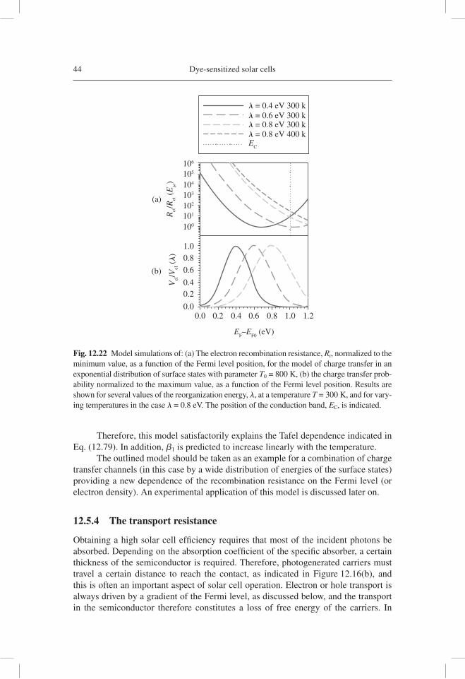
44 Dye-sensitized solar cells
Therefore, this model satisfactorily explains the Tafel dependence indicated in Eq. (12.79). In addition, b1 is predicted to increase linearly with the temperature.
The outlined model should be taken as an example for a combination of charge transfer channels (in this case by a wide distribution of energies of the surface states) providing a new dependence of the recombination resistance on the Fermi level (or electron density). An experimental application of this model is discussed later on.
12.5.4 The transport resistance
Obtaining a high solar cell effi ciency requires that most of the incident photons be absorbed. Depending on the absorption coeffi cient of the specifi c absorber, a certain thickness of the semiconductor is required. Therefore, photogenerated carriers must travel a certain distance to reach the contact, as indicated in Figure 12.16(b), and this is often an important aspect of solar cell operation. Electron or hole transport is always driven by a gradient of the Fermi level, as discussed below, and the transport in the semiconductor therefore constitutes a loss of free energy of the carriers. In
l = 0.4 eV 300 kl = 0.6 eV 300 kl = 0.8 eV 300 kl = 0.8 eV 400 k
106
105
104
103
102(a)
(b)
101
100
1.00.8
0.6
0.40.2
0.00.0 0.2 0.4
EF–E
F0 (eV)
Vel/V
el (l
)R
ct/R
ct (
Em)
0.6 0.8 1.0 1.2
EC
Fig. 12.22 Model simulations of: (a) The electron recombination resistance, Rr, normalized to the minimum value, as a function of the Fermi level position, for the model of charge transfer in an exponential distribution of surface states with parameter T0 = 800 K, (b) the charge transfer prob-ability normalized to the maximum value, as a function of the Fermi level position. Results are shown for several values of the reorganization energy, l, at a temperature T = 300 K, and for vary-ing temperatures in the case l = 0.8 eV. The position of the conduction band, EC, is indicated.
Impedance spectroscopy 45
addition, the extraction of carriers to provide a photocurrent in the external circuit is in competition with recombination processes. It is therefore important to determine the basic transport coeffi cients of the electronic carriers, such as the mobility, un, and the diffusion coeffi cient, Dn, since this allows us to evaluate the energy losses associ-ated with carrier transport and the diffusion length. The basic quantity that describes the transport features in IS is a transport resistance, rt. A description of the method to obtain Dn from rt is presented below.
Diffusion under concentration gradients is a collective phenomenon, and in DSC as well as in disordered materials in general, diffusion involves electronic states with widely varying energies [12.61]. A clear manifestation of this is the fact that, in DSC, the diffusion coeffi cient varies several orders of magnitude under modifi cation of bias voltage [12.56]. It is therefore useful to carefully establish the meaning of measured transport quantities.
To discuss the motion of electrons in a semiconductor material, with concentra-tion n(x) at position x, we assume that the Fermi level, or electrochemical potential, of the electrons has two basic components [12.60, 12.107]:
EFn = Ec + mn (12.93)
The fi rst one, Ec, is the energy of the edge of the conduction band (or transport level), which can be associated to the Galvani (electrostatic) potential, f, with respect to some suitable reference level, as follows:
EC = −qf (12.94)
The second component in Eq. (12.93), mn, is the chemical potential of electrons. This is an entropic contribution that accounts for the dispersion of the carriers over all the available sites, and can normally be formulated in terms of the carrier density. If the species is randomly distributed in the available sites, the following expression, which is equivalent to Eq. (12.67), holds:
mn B
c
=−
k Tn
N nln (12.95)
If the sites are far from saturated, we obtain the ideal statistics:
mn B
c
= k Tn
Nln (12.96)
which is equivalent to Eq. (12.15). Eqs. (12.95) and (12.96) are very important instances of the chemical potential, but, more generally, the diffusion theory formu-lated below is valid for any mn.
Let us now consider the system of main interest here: a nanostructured metal-oxide semiconductor, surrounded with electrolyte that contains abundant ionic spe-cies of both change signs. Figure 12.23(a) shows a scheme of such a semiconductor in equilibrium. When a bias voltage, V, is applied in the substrate, two basic sit-uations may occur, as shown in Figures 12.23(b) and (c). Note that the voltage V in these fi gures is positive according to the convention of photovoltage used in this chapter, but that it is negative according to the usual convention of electrochemistry. In Figure 12.23(b), the voltage causes a change of the concentration of the electrons
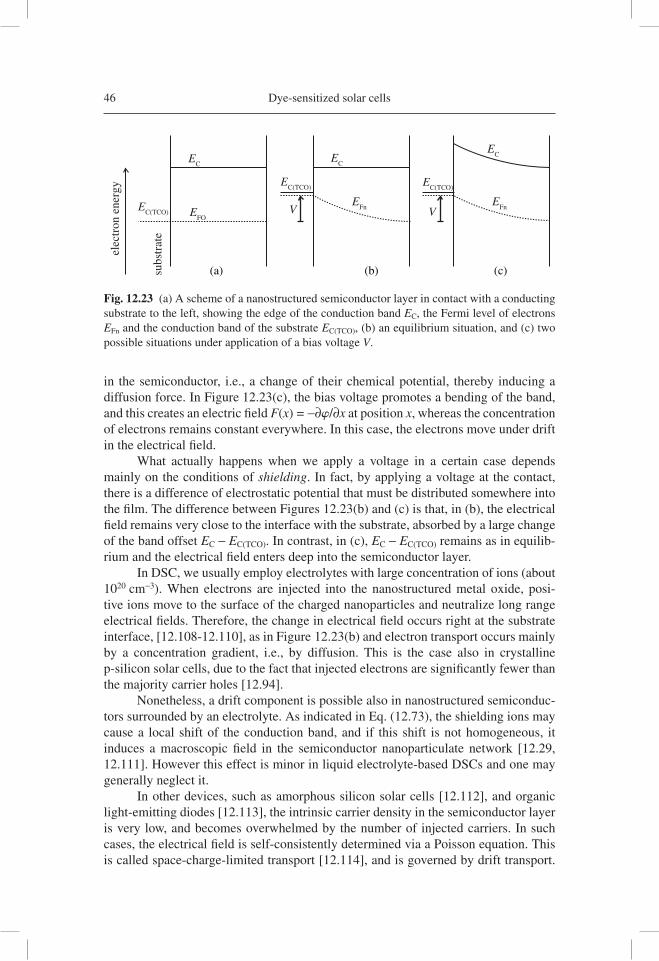
46 Dye-sensitized solar cells
in the semiconductor, i.e., a change of their chemical potential, thereby inducing a diffusion force. In Figure 12.23(c), the bias voltage promotes a bending of the band, and this creates an electric fi eld F(x) = −∂w/∂x at position x, whereas the concentration of electrons remains constant everywhere. In this case, the electrons move under drift in the electrical fi eld.
What actually happens when we apply a voltage in a certain case depends mainly on the conditions of shielding. In fact, by applying a voltage at the contact, there is a difference of electrostatic potential that must be distributed somewhere into the fi lm. The difference between Figures 12.23(b) and (c) is that, in (b), the electrical fi eld remains very close to the interface with the substrate, absorbed by a large change of the band offset EC − EC(TCO). In contrast, in (c), EC − EC(TCO) remains as in equilib-rium and the electrical fi eld enters deep into the semiconductor layer.
In DSC, we usually employ electrolytes with large concentration of ions (about 1020 cm−3). When electrons are injected into the nanostructured metal oxide, posi-tive ions move to the surface of the charged nanoparticles and neutralize long range electrical fi elds. Therefore, the change in electrical fi eld occurs right at the substrate interface, [12.108-12.110], as in Figure 12.23(b) and electron transport occurs mainly by a concentration gradient, i.e., by diffusion. This is the case also in crystalline p-silicon solar cells, due to the fact that injected electrons are signifi cantly fewer than the majority carrier holes [12.94].
Nonetheless, a drift component is possible also in nanostructured semiconduc-tors surrounded by an electrolyte. As indicated in Eq. (12.73), the shielding ions may cause a local shift of the conduction band, and if this shift is not homogeneous, it induces a macroscopic fi eld in the semiconductor nanoparticulate network [12.29, 12.111]. However this effect is minor in liquid electrolyte-based DSCs and one may generally neglect it.
In other devices, such as amorphous silicon solar cells [12.112], and organic light-emitting diodes [12.113], the intrinsic carrier density in the semiconductor layer is very low, and becomes overwhelmed by the number of injected carriers. In such cases, the electrical fi eld is self-consistently determined via a Poisson equation. This is called space-charge-limited transport [12.114], and is governed by drift transport.
EC
subs
trat
e
elec
tron
ene
rgy
VV
EC
EC
EFO
EFn
EFn
EC(TCO)
EC(TCO)
EC(TCO)
(b) (c)(a)
Fig. 12.23 (a) A scheme of a nanostructured semiconductor layer in contact with a conducting substrate to the left, showing the edge of the conduction band EC, the Fermi level of electrons EFn and the conduction band of the substrate EC(TCO), (b) an equilibrium situation, and (c) two possible situations under application of a bias voltage V.
Impedance spectroscopy 47
In a certain sense, it is an opposite extreme of a transport situation, as compared to diffusion.
Diffusion
Turning our attention to the dominant conditions in DSC, we now analyze the dif-fusive transport of electrons [12.58, 12.60, 12.61]. The driving force for diffusion is the gradient of the chemical potential of the electrons. In simple terms, there are two forms of the diffusion law:
1. In the Onsager form, a linear relationship is assumed [12.115] between the diffusive fl ux and the gradient of the chemical potential:
J
nu
q xnn n= −
∂∂m
(12.97)
The prefactor Ln = nun/q is known as the Onsager coeffi cient.
2. In the Fick form, diffusion is formulated in terms of the concentration gradient
J D
n
xn n= − ∂∂
(12.98)
The coeffi cient Dn in Eq. (12.98) is called the chemical diffusion coeffi cient [12.116, 12.117]. By comparing Eqs. (12.97) and (12.98), we obtain the expression:
Dk T
qu
n
k T nnB
nB
n=⎛⎝⎜
⎞⎠⎟
∂∂
⎛⎝⎜
⎞⎠⎟
m (12.99)
Here, Dn contains two components: (i) a phenomenological coeffi cient un (the mobility) and (ii) the term n∂mn/∂n, accounting for the difference between a gradient in concentration, and a gradient in chemical potential. This last term is expressed in dimensionless form as the thermodynamic factor introduced by Darken [12.118]:
χn
B
n=∂∂
n
k T n
m (12.100)
The thermodynamic factor can, with respect to the chemical capacitance, be expressed as:
χnB
= q n
k T C
2 1
m
(12.101)
Another way to approach the diffusion coeffi cient is to monitor the random walks of the electronic carriers. The resulting coeffi cient is termed the jump (or kinetic) diffusion coeffi cient, and is simply proportional to the mobility:
D
k T
quJ
Bn= (12.102)
48 Dye-sensitized solar cells
It should be emphasized that DJ is closely related to the tracer diffusion coef-fi cient, D*. We can now write the chemical diffusion coeffi cient as the product:
Dn = χnDJ (12.103)
Alternatively, we have:
D
k T
qun
Bn n= χ (12.104)
Eq. (12.103) is a statement of the generalized Einstein relation [12.61].The electron conductivity is:
sn = nqun (12.105)
Using Eqs. (12.101), (12.104) and (12.105), the conductivity can be expressed in terms of the chemical diffusion coeffi cient and the chemical capacitance as:
sn = cmDn (12.106)
Diffusion and drift
As mentioned above, in a system in which the electrochemical potential has the two components indicated in Eq. (12.93), we may view the electrical current as composed of the sum of conduction and diffusion currents:
j qnu F qD
n
xn n n= + ∂∂
(12.107)
Now, Eq. (12.107) can be written as:
j nu
E
xn nFn= −
∂∂
(12.108)
This relationship states that the electrical current associated with one kind of carrier is proportional to the gradient of the electrochemical potential, EFn. Such an approach is usually employed in electronic device modeling [12.25, 12.29].
The transport resistance
We can now obtain an expression for the transport resistance that we measure in IS. We recall that we are interested in systems, such as a semiconductor layer of thickness L, which may be far from homogeneous in terms of the carrier distribution. We there-fore want to determine the resistance, associated with a specifi c kind of carrier (e.g., electrons), in a small spatial distance Δx. Associated with this distance, is a differ-ence of electrochemical potential, which may be expressed as a difference in voltage: ΔEFn = qΔwn, see Eq. (12.50). Applying the transport equation, (12.108), we obtain:
j
xn nn= −s
ΔΔw
(12.109)
Impedance spectroscopy 49
and therefore:
R
Aj
x
A ptn
n n
= − =−
Δ Δw
( )1 s (12.110)
In Eq. (12.110), we appreciate that the transport resistance depends on the geo-metric dimensions of the semiconductor slab, and on the reciprocal conductivity.
Transport in a single level
Let us consider a semiconductor with a single transport level, in which the electron carriers are free from interactions. In this case, the relation between the electrochemi-cal potential and the carrier density is simply given by Maxwell-Boltzmann statis-tics, Eq. (12.17). Since this is the ideal statistics, the thermodynamic factor, chemical diffusion coeffi cient, etc., become considerably simplifi ed [12.61]. We have χn = 1, thus Dn = DJ = D0, and we thus obtain Eq. (12.7) as well as the standard Einstein rela-tion relating diffusivity with mobility:
D
k T
qun
Bn= (12.111)
Multiple trapping transport
In classical multiple trapping transport [12.119-12.121], we distinguish between two classes of electronic states: the transport states above the mobility edge (that may be associated with extended states in the conduction band), and localized states in the bandgap. The multiple-trapping model describes the effect of trap levels over the rate of displacement through transport states. Such an effect can be analyzed using the full set of transport-kinetic equations of the model, which provides the system’s response under any required set of conditions. However, if trapping and detrapping are fast processes, we apply the quasi-equilibrium approach that was discussed above in the analysis of surface states. Subsequently, electron trapping kinetics can be read-ily described in terms of electron densities in transport and trap states, and this second approach will be adopted herein [12.40]. In fact, a detailed analysis [12.75] shows that the fi rst, general, approach reduces to the second one whenever the traps can be considered in quasi-equilibrium conditions.
In the transport states, we have a number of carriers, ncb, and a chemical capacitance, cm
cb. Assuming ideal statistics, jump and chemical diffusion coeffi cients, we have D D DJ
cbncb= = 0. The localized states (below the mobility edge), have a distri-
bution gL(E), a number of carriers, nL, and a chemical capacitance cmtraps. The relation-
ships for the total carrier density and total chemical capacitance are, respectively:
n = ncb + nL (12.112)
c c c cn
nm m m m= + = +∂∂
⎛⎝⎜
⎞⎠⎟
cb traps cb L
cb
1 (12.113)
50 Dye-sensitized solar cells
It can be shown [12.61] that the jump diffusion coeffi cient is given by:
D
n
nDJ
cb= 0 (12.114)
The thermodynamic factor can be written as:
χnL
cb
= +∂∂
⎛⎝⎜
⎞⎠⎟
−
11
n
n (12.115)
Hence, the chemical diffusion coeffi cient has the general form [12.58]:
Dn
nDn
L
cb
== +∂∂
⎛⎝⎜
⎞⎠⎟
−
11
0 (12.116)
Alternatively, we can write Eq. (12.116) as:
Dc E
c E c EDn
cbFn
cbFn
trapsFn
=+m
m m
( )
( ) ( ) 0 (12.117)
The effect of trapping in the chemical diffusion coeffi cient is dominant when ∂nL/∂ncb >> 1. In this case the result becomes:
Dn
nDn
cb
L
=∂∂
⎛⎝⎜
⎞⎠⎟ 0 (12.118)
or alternatively:
Dc E
c EDn
cbFn
trapsFn
= m
m
( )
( ) 0 (12.119)
Eq. (12.118) shows that the chemical diffusion coeffi cient in the presence of traps is reduced by the relationship of the number of free to trapped electrons for a small variation of the Fermi level.
We obtain the following result for the conductivity:
s mn n
traps= D c (12.120)
This last equation is a formulation of the generalized Einstein relation link-ing the conductivity, the chemical diffusion coeffi cient and the chemical capacitance [12.61, 12.122].
Impedance spectroscopy 51
We can also express the conductivity in terms of the carrier density and jump diffusion coeffi cient:
sn
B
cb
B
= =q n
k TD
q n
k TDJ
2 2
0 (10.121)
Equation (12.120) can also be written as s mn D c= 0cb. This shows that, in the
multiple trapping model, the conductivity is determined exclusively by the trans-port level and is completely independent of the presence and distribution of traps. The steady-state conduction is not affected by the trapping process, due to the traps remaining in equilibrium.
Multiple trapping in exponential distribution
As mentioned before, it is well established that nanostructured (anatase) TiO2 used in DSC shows this type of distribution of states in the bandgap [12.51, 12.53, 12.83, 12.84, 12.123]. We discuss the regime of electrochemical potentials in which the Fermi level is well below the conduction band. Hence, the free electron density is much lower than the number of trapped electrons, ncb/nL << 1. It is easy to show [12.61] that the thermodynamic factor is constant [12.58]:
χn
cb
cb
L
=∂∂
= −n
n
n
na
1 (12.122)
Here, a = T/T0 For typical values of T0, χn ≈ 5 at room temperature. The cal-culation of the jump and chemical diffusion coeffi cient, gives, respectively [12.58, 12.61]:
DJ = aDn (12.123)
DN T
N TE E
k T k TDn
c
LFn c
B B
= − −⎛⎝⎜
⎞⎠⎟
⎡
⎣⎢
⎤
⎦⎥0
00
1 1exp ( ) (12.124)
The diffusion length is usually defi ned for transport in a single level, as:
L Dn
00 0= t (12.125)
where t0 is the electron lifetime. Ln0 is a very useful quantity which indicates the aver-
age distance that an electron travels before undergoing a recombination event.Transient techniques that induce a gradient of the Fermi level, such as IS, IMPS,
etc., provide a determination of the chemical diffusion coeffi cient [12.124]. Therefore, we do not experimentally have direct access to D0. Similarly, when we measure the electron lifetime by transient methods, we do not directly observe the decay time of carriers in the transport level. Using again a quasi-equilibrium approach, the trapping and detrapping effects introduce a delay factor leading to the measured quantity being a response time [12.40]
52 Dye-sensitized solar cells
t tnL
cb
== +∂∂
⎛⎝⎜
⎞⎠⎟
1 0
n
n (12.126)
If the carrier density is homogeneous, we can defi ne a diffusion length Ln from the measured parameters Dn and tn. By combining Eqs. (12.116), (12.125) and (12.126), we obtain:
L D Ln n n n= =t 0 (12.127)
The time constants determined by the transient or frequency techniques can thus be used to calculate the diffusion length in Eq. (12.125). Eq. (12.127) implies that, despite the variation of Dn and tn, the diffusion length should be constant, since the variation of both quantities has the same origin in the delay by trapping factors [12.40]. However, Eq. (12.127) should be used with some points of caution: (1) the time constants depend on local conditions of the carrier density (or Fermi level), and both Dn and tn should therefore be determined under equivalent conditions [12.125] (2) the free carrier lifetime t0 in Eq. (12.126) may include also a combination of processes by the different electron transfer channels as discussed in Sec. 10.5.3. Such a variation of t0 with voltage has no counterpart in Dn and for this reason, Ln will not be constant.
12.6 TRANSMISSION LINE MODELS
12.6.1 General structure of transmission lines
Transmission line (TL)-equivalent circuits, such as those shown in Figure 12.1, are frequently used in electrochemistry in connection with porous electrodes or diffusion in active electrodes [12.41, 12.43, 12.46, 12.126-12.128]. Models for nanostructured semiconductor electrodes used in DSC are described in Refs. [12.46, 12.47, 12.49, 12.129].
The use of TL-equivalent circuits in solar cells is a consequence of the neces-sary spatial extension of the absorber to optimize the capture of the solar photons. This introduces the need to transport the photogenerated carriers towards the external contacts, as mentioned in Sec. 12.5.4. The situation, indicating the different elec-tronic processes in an extended solar cell, is schematically shown in Figure 12.24(a). Carriers that are generated must travel to the contact and this process competes with recombination. In addition, the outer contacts often introduce major recombination sites that should be controlled separately, since the recombination mechanism is usu-ally different at these points.
The structure depicted in Figure 12.24(a) is a basic outline and can be realized in various ways. For example, in crystalline Si solar cells, electron and hole carriers travel in the same medium, and recombination at the back surface is a major point of concern [12.94]. Nanostructured hybrid solar cells and organic solar cells rapidly separate the charges to different transport media. Electrons and holes thus travel in separate material phases [12.33], while the transport is intercepted by charge transfer
Impedance spectroscopy 53
events. We take Figure 12.24(a) as a basic reference to generally discuss the imped-ance models of solar cells with outer planar contacts.
Intuitively, one can see that the local processes that where discussed in the fundamental model of Sec. 12.4.1 and Figure 12.13, i.e., recombination resistance and chemical capacitance, are also present everywhere in Figure 12.24(a). However, due to the spatial extension, additional impedances are required in order to transfer the carrier from one point to a neighboring one [12.130]. There are, consequently, two horizontal channels for transport, corresponding to each kind of carrier. One thus obtains the connection of Figure 12.24(b), which is a TL. The TL model includes specifi c elements at the boundaries which account for the particular properties of recombination, at the point where one carrier should be blocked, and the other
3
light absorber
EC
EFn
EFp
EV
elec
tron
sel
ectiv
eco
ntac
t
hole
sele
ctiv
e co
ntac
t
1
0
4
(a)
(b)
(c)
L
X
6
25
3
1
4
6
2
5Z
B
rr
Cm
x1
z z z z z
x1
x1
x2
x2
x2
x1
x1
x2
x2
ZA
Fig. 12.24 (a) A basic energy diagram of a solar cell showing the main electronic processes: (1) generation, (2) bulk recombination, (3) electron transport, (4) hole transport, (5) recombination of electrons at the hole-selective contact, (6) recombination of holes at the electron- selective con-tact. (b) The general transmission-line-equivalent circuit. (c) The local RC-equivalent circuit.
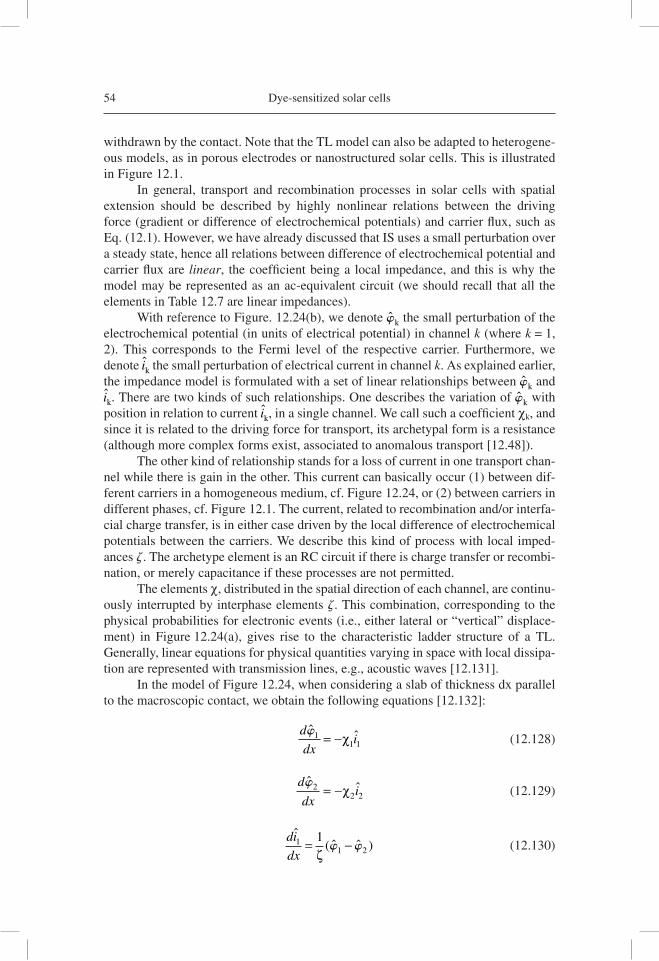
54 Dye-sensitized solar cells
withdrawn by the contact. Note that the TL model can also be adapted to heterogene-ous models, as in porous electrodes or nanostructured solar cells. This is illustrated in Figure 12.1.
In general, transport and recombination processes in solar cells with spatial extension should be described by highly nonlinear relations between the driving force (gradient or difference of electrochemical potentials) and carrier fl ux, such as Eq. (12.1). However, we have already discussed that IS uses a small perturbation over a steady state, hence all relations between difference of electrochemical potential and carrier fl ux are linear, the coeffi cient being a local impedance, and this is why the model may be represented as an ac-equivalent circuit (we should recall that all the elements in Table 12.7 are linear impedances).
With reference to Figure. 12.24(b), we denote wk the small perturbation of the electrochemical potential (in units of electrical potential) in channel k (where k = 1, 2). This corresponds to the Fermi level of the respective carrier. Furthermore, we denote ik the small perturbation of electrical current in channel k. As explained earlier, the impedance model is formulated with a set of linear relationships between wk and ik. There are two kinds of such relationships. One describes the variation of wk with position in relation to current ik, in a single channel. We call such a coeffi cient χk, and since it is related to the driving force for transport, its archetypal form is a resistance (although more complex forms exist, associated to anomalous transport [12.48]).
The other kind of relationship stands for a loss of current in one transport chan-nel while there is gain in the other. This current can basically occur (1) between dif-ferent carriers in a homogeneous medium, cf. Figure 12.24, or (2) between carriers in different phases, cf. Figure 12.1. The current, related to recombination and/or interfa-cial charge transfer, is in either case driven by the local difference of electrochemical potentials between the carriers. We describe this kind of process with local imped-ances z. The archetype element is an RC circuit if there is charge transfer or recombi-nation, or merely capacitance if these processes are not permitted.
The elements χ, distributed in the spatial direction of each channel, are continu-ously interrupted by interphase elements z. This combination, corresponding to the physical probabilities for electronic events (i.e., either lateral or “vertical” displace-ment) in Figure 12.24(a), gives rise to the characteristic ladder structure of a TL. Generally, linear equations for physical quantities varying in space with local dissipa-tion are represented with transmission lines, e.g., acoustic waves [12.131].
In the model of Figure 12.24, when considering a slab of thickness dx parallel to the macroscopic contact, we obtain the following equations [12.132]:
d
dxi
ˆ ˆw11 1= −χ (12.128)
d
dxi
ˆ ˆw22 2= −χ (12.129)
di
dx
ˆ( ˆ ˆ )1
1 2
1= −ζw w (12.130)
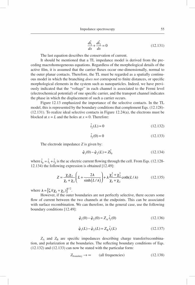
Impedance spectroscopy 55
di
dx
di
dx
ˆ ˆ1 2 0+ = (12.131)
The last equation describes the conservation of current.It should be mentioned that a TL impedance model is derived from the pre-
ceding macrohomogeneous equations. Regardless of the morphological details of the active fi lm, it is assumed that the carrier fl uxes occur one-dimensionally, normal to the outer planar contacts. Therefore, the TL must be regarded as a spatially continu-ous model in which the branching does not correspond to fi nite distances, or specifi c morphological elements in the system such as nanoparticles. Indeed, we have previ-ously indicated that the “voltage” in each channel is associated to the Fermi level (electrochemical potential) of one specifi c carrier, and the transport channel indicates the phase in which the displacement of such a carrier occurs.
Figure 12.13 emphasized the importance of the selective contacts. In the TL model, this is represented by the boundary conditions that complement Eqs. (12.128)-(12.131). To realize ideal selective contacts in Figure 12.24(a), the electrons must be blocked at x = L and the holes at x = 0. Therefore:
ˆ ( )i L2 0= (12.132)
ˆ ( )i2 0 0= (12.133)
The electrode impedance Z is given by:
ˆ ( ) ˆ ( ) ˆw w1 2 00 − =L Zi (12.134)
where ˆ ˆ ˆi i i0 1 2= + is the ac electric current fl owing through the cell. From Eqs. (12.128-12.134) the following expression is obtained [12.49]:
Z LL
L=+
+ ( )⎛
⎝⎜⎞
⎠⎟+
++
χ χχ χ
χ χχ χ
1 2
1 2
12
22
1 2
2l
ll l
sinh /coth( / ) (12.135)
where l = +[ ]ζ χ χ/( )/
1 21 2
.However, if the outer boundaries are not perfectly selective, there occurs some
fl ow of current between the two channels at the endpoints. This can be associated with surface recombination. We can therefore, in the general case, use the following boundary conditions [12.49]:
ˆ ( ) ˆ ( ) ˆ ( )w w1 2 20 0 0− = Z iA (12.136)
ˆ ( ) ˆ ( ) ˆ ( )w w1 2 1L L Z i L− = B (12.137)
ZA and ZB are specifi c impedances describing charge transfer/recombina-tion, and polarization at the boundaries. The refl ecting boundary conditions of Eqs. (12.132) and (12.133) can now be stated with the particular form:
Zboundary → ∞ (all frequencies) (12.138)
56 Dye-sensitized solar cells
where boundary = A, B. Notice that the refl ecting boundary condition of Eq. (12.138) corresponds to an open circuit.
The general expression of the TL model with the generalized boundary condi-tions is [12.49]:
Z S Z Z C Z Z S
L
=+
+ + + ++
⎡
⎣⎢
⎤
⎦⎥
−1 1
1 21 2
1 2
1
χ χχ χ
χ χl
ll l l( ) ( )
( )A B A B
ll l ll l l l lχ χ χ χ χ χ χ χ χ χ1 2 1 2 1 1 2 2 2 1
1
( )+ + +[ ] + +[ ]{+
S S L C Z S L C ZA B
χχ χ
χ χ χ χ χ χ1 2
1 2 12
22
1 22+
+ + +⎡⎣⎢
⎤⎦⎥
⎫⎬⎭
( )CL
S Z Zl ll
A B
(12.139)
where the shorthand notations Cl = cosh(L/l) and Sl = sinh(L/l) have been used.Several particular cases of Eq. (12.139) can be examined.First, if we have the following conditions: (i) ZA → ∞ and ZB → ∞ at all frequen-
cies and (ii) a large conductivity in channel 2 so that the lower transport channel becomes short-circuited, then the standard double-channel TL of Eq. (12.135) is recovered.
Second, we assume again two conditions: (i) ZA → ∞ (refl ecting boundary) and (ii) large conductivity in channel 2 so that the lower transport channel becomes short-circuited, i.e., χ2 = 0. In this case, we obtain the TL shown in Figure 12.25(b). The following expression results:
Z
Z L
Z L=
++
ll
l lχ
λχχ1
1
1
B
B
coth( / )
coth( / ) (12.140)
This model is also applied for diffusion with a special boundary condition [12.133].
Next we apply blocking boundary conditions at both ends of the transport chan-nels in the TL. We set ZA → ∞, ZB → ∞ in Eq. (12.140), and χ2 = 0 in Eq. (12.135), and obtain the TL shown in Figure 12.25(a), with an impedance
Z = lχ1 coth(L/l) (12.141)
Experimentally, it is no easy task to separate the transport elements in both channels of the TL [12.134]. Normally, one channel is much more conducting than the other, and thus the simple expression in Eq. (12.141) is undoubtedly the most widely used type of TL model.
Finally, Figure 12.25(c) shows the case in which the generalized boundary con-dition is at the end of the more conductive transport channel. Note that the TL imped-ance is simply the parallel connection of ZA and Eq. (12.141).
TL models with three transport channels have also been solved analytically [12.129].
12.6.2 General diffusion transmission lines
We turn our attention to the scheme of a DSC in Figure 12.16(b), where electrons diffuse in a nanostructured semiconductor surrounded with redox electrolyte that
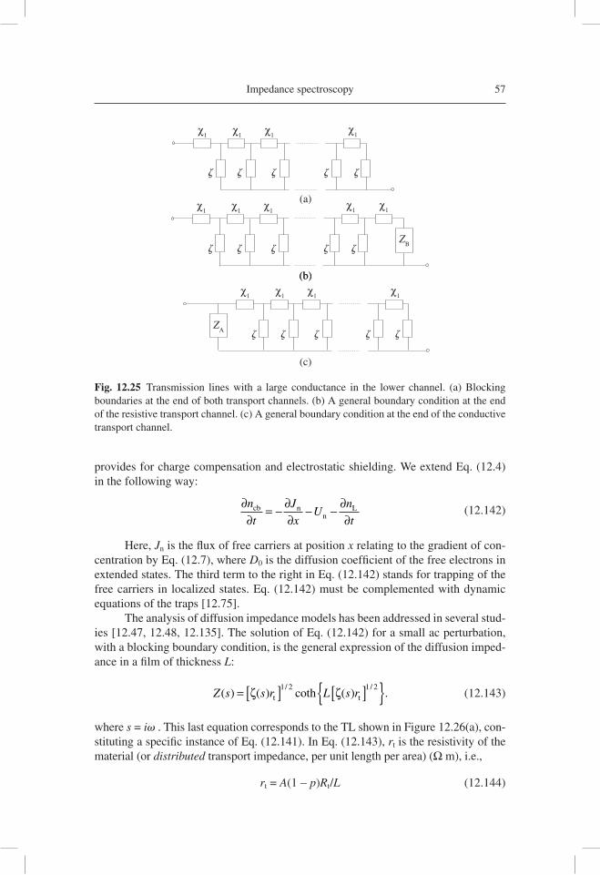
Impedance spectroscopy 57
provides for charge compensation and electrostatic shielding. We extend Eq. (12.4) in the following way:
∂∂
= −∂∂
− −∂∂
n
t
J
xU
n
tcb n
nL (12.142)
Here, Jn is the fl ux of free carriers at position x relating to the gradient of con-centration by Eq. (12.7), where D0 is the diffusion coeffi cient of the free electrons in extended states. The third term to the right in Eq. (12.142) stands for trapping of the free carriers in localized states. Eq. (12.142) must be complemented with dynamic equations of the traps [12.75].
The analysis of diffusion impedance models has been addressed in several stud-ies [12.47, 12.48, 12.135]. The solution of Eq. (12.142) for a small ac perturbation, with a blocking boundary condition, is the general expression of the diffusion imped-ance in a fi lm of thickness L:
Z s s r L s r( ) ( ) coth ( ) .
/ /= [ ] [ ]{ }ζ ζt t1 2 1 2
(12.143)
where s = iv . This last equation corresponds to the TL shown in Figure 12.26(a), con-stituting a specifi c instance of Eq. (12.141). In Eq. (12.143), rt is the resistivity of the material (or distributed transport impedance, per unit length per area) (Ω m), i.e.,
rt = A(1 − p)Rt/L (12.144)
χ1
χ1 χ1 χ1 χ1
χ1 χ1 χ1 χ1
z
z
z z z z z
z z z z
z z z z
ΖB
ΖA
χ1 χ1 χ1 χ1
(a)
(b)(b)
(c)
ZB
ZA
Fig. 12.25 Transmission lines with a large conductance in the lower channel. (a) Blocking boundaries at the end of both transport channels. (b) A general boundary condition at the end of the resistive transport channel. (c) A general boundary condition at the end of the conductive transport channel.
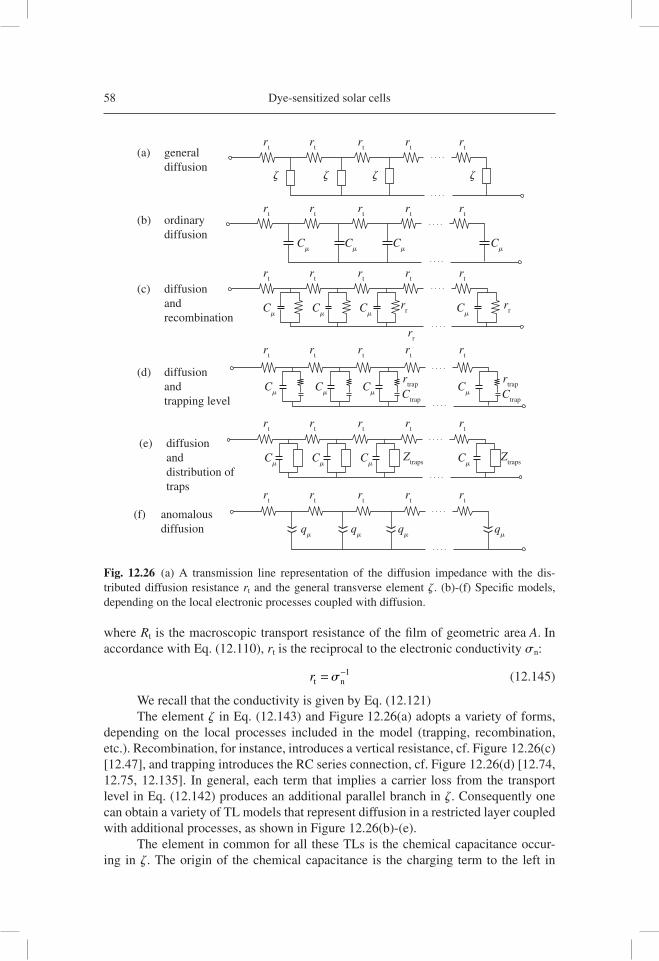
58 Dye-sensitized solar cells
where Rt is the macroscopic transport resistance of the fi lm of geometric area A. In accordance with Eq. (12.110), rt is the reciprocal to the electronic conductivity sn:
rt n= −s
1 (12.145)
We recall that the conductivity is given by Eq. (12.121)The element z in Eq. (12.143) and Figure 12.26(a) adopts a variety of forms,
depending on the local processes included in the model (trapping, recombination, etc.). Recombination, for instance, introduces a vertical resistance, cf. Figure 12.26(c) [12.47], and trapping introduces the RC series connection, cf. Figure 12.26(d) [12.74, 12.75, 12.135]. In general, each term that implies a carrier loss from the transport level in Eq. (12.142) produces an additional parallel branch in z. Consequently one can obtain a variety of TL models that represent diffusion in a restricted layer coupled with additional processes, as shown in Figure 12.26(b)-(e).
The element in common for all these TLs is the chemical capacitance occur-ing in z. The origin of the chemical capacitance is the charging term to the left in
rt
rt
rt
rt
rt
rt
rt
Cm
Cm
Cm
Cm
Cm
Cm
Cm
qm
qm
qm
qm
Cm
Cm
Cm
Cm
Cm
Cm
Cm
Cm
rt
rt
rt
rt
rt
rt
rt
rr
rr
rr
rt
rt
rt
rt
rt
rtrap
Ctrap
Ztraps C
mZ
traps
rtrap
Ctrap
rt
rt
rt
rt
rt
rt
rt
rt
rt
rt
rt
zzzz
(a) general diffusion
(b) ordinary diffusion
(c) diffusion and recombination
(d) diffusion and trapping level
(e) diffusion and distribution of traps
(f) anomalous diffusion
Fig. 12.26 (a) A transmission line representation of the diffusion impedance with the dis-tributed diffusion resistance rt and the general transverse element z. (b)-(f) Specifi c models, depending on the local electronic processes coupled with diffusion.
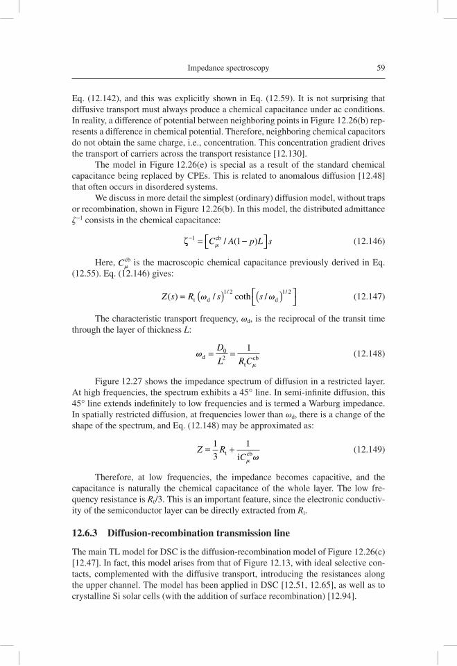
Impedance spectroscopy 59
Eq. (12.142), and this was explicitly shown in Eq. (12.59). It is not surprising that diffusive transport must always produce a chemical capacitance under ac conditions. In reality, a difference of potential between neighboring points in Figure 12.26(b) rep-resents a difference in chemical potential. Therefore, neighboring chemical capacitors do not obtain the same charge, i.e., concentration. This concentration gradient drives the transport of carriers across the transport resistance [12.130].
The model in Figure 12.26(e) is special as a result of the standard chemical capacitance being replaced by CPEs. This is related to anomalous diffusion [12.48] that often occurs in disordered systems.
We discuss in more detail the simplest (ordinary) diffusion model, without traps or recombination, shown in Figure 12.26(b). In this model, the distributed admittance z−1 consists in the chemical capacitance:
ζ− = −⎡⎣ ⎤⎦
1 1C A p L sm
cb / ( ) (12.146)
Here, Cmcb is the macroscopic chemical capacitance previously derived in Eq.
(12.55). Eq. (12.146) gives:
Z s R s s( ) / coth /
/ /= ( ) ( )⎡⎣
⎤⎦t v vd d
1 2 1 2 (12.147)
The characteristic transport frequency, vd, is the reciprocal of the transit time through the layer of thickness L:
vdt
cb= =
D
L R C02
1
m
(12.148)
Figure 12.27 shows the impedance spectrum of diffusion in a restricted layer. At high frequencies, the spectrum exhibits a 45° line. In semi-infi nite diffusion, this 45° line extends indefi nitely to low frequencies and is termed a Warburg impedance. In spatially restricted diffusion, at frequencies lower than vd, there is a change of the shape of the spectrum, and Eq. (12.148) may be approximated as:
Z RC
= +1
3
1t cbi m v
(12.149)
Therefore, at low frequencies, the impedance becomes capacitive, and the capacitance is naturally the chemical capacitance of the whole layer. The low fre-quency resistance is Rt/3. This is an important feature, since the electronic conductiv-ity of the semiconductor layer can be directly extracted from Rt.
12.6.3 Diffusion-recombination transmission line
The main TL model for DSC is the diffusion-recombination model of Figure 12.26(c) [12.47]. In fact, this model arises from that of Figure 12.13, with ideal selective con-tacts, complemented with the diffusive transport, introducing the resistances along the upper channel. The model has been applied in DSC [12.51, 12.65], as well as to crystalline Si solar cells (with the addition of surface recombination) [12.94].
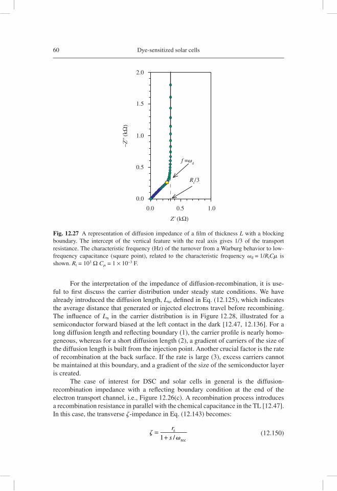
60 Dye-sensitized solar cells
For the interpretation of the impedance of diffusion-recombination, it is use-ful to fi rst discuss the carrier distribution under steady state conditions. We have already introduced the diffusion length, Ln, defi ned in Eq. (12.125), which indicates the average distance that generated or injected electrons travel before recombining. The infl uence of Ln in the carrier distribution is in Figure 12.28, illustrated for a semiconductor forward biased at the left contact in the dark [12.47, 12.136]. For a long diffusion length and refl ecting boundary (1), the carrier profi le is nearly homo-geneous, whereas for a short diffusion length (2), a gradient of carriers of the size of the diffusion length is built from the injection point. Another crucial factor is the rate of recombination at the back surface. If the rate is large (3), excess carriers cannot be maintained at this boundary, and a gradient of the size of the semiconductor layer is created.
The case of interest for DSC and solar cells in general is the diffusion- recombination impedance with a refl ecting boundary condition at the end of the electron transport channel, i.e., Figure 12.26(c). A recombination process introduces a recombination resistance in parallel with the chemical capacitance in the TL [12.47]. In this case, the transverse z-impedance in Eq. (12.143) becomes:
z
v=
r
sr
1 rec+ / (12.150)
0.0
0.0
0.5
1.0
1.5
2.0
0.5 1.0
–Z"
(kΩ
)
Z' (kΩ)
f =vd
Rt/3
Fig. 12.27 A representation of diffusion impedance of a fi lm of thickness L with a blocking boundary. The intercept of the vertical feature with the real axis gives 1/3 of the transport resistance. The characteristic frequency (Hz) of the turnover from a Warburg behavior to low-frequency capacitance (square point), related to the characteristic frequency vd = 1/RtCm is shown. Rt = 103 Ω Cm = 1 × 10⁻³ F.
Impedance spectroscopy 61
The characteristic frequency of recombination is:
vrec = −t0
1 (12.151)
where t0 is the free electron lifetime, and the distributed recombination resistance is given by:
r LA p R LA pCr r= − = −( ) ( )1 1 0t
m
(12.152)
Here, Rr is the macroscopic recombination resistance of the layer, as discussed in Sec. 12.5.3. The impedance adopts the form [12.47]:
ZR R
R R( )/
coth / //
/ /v
v vv v=
+⎛⎝⎜
⎞⎠⎟
( ) ( )⎡⎣
⎤t r
rect r rec1 i
1 i1 2
1 2 1 2+ ⎦⎦ (12.153)
The impedance spectra of the model of Eq. (12.153) are shown in Figure 12.29. In contrast with Figure 12.27, the spectra of diffusion-recombination are resistive at low frequencies. This is due to the fact that recombination introduces a dc conduction path. There are now two competing processes: the transport across the layer (vd) and the carrier loss by recombination (vrec). The shape of the spectra is regulated by the factor relating the characteristic frequencies, that can be expressed in several alterna-tive ways [12.47]:
v
v
d
rec
r
t
= = ⎛⎝⎜
⎞⎠⎟
R
R
L
Ln
2
(12.154)
The diffusion-recombination impedance provides two basic kinds of spectra, according to the conditions of Eq. (12.154). The spectrum for Rt < Rr, presented in
position x0 L
Ln
n0
nS 1
23
Bac
k co
ntac
t
Fron
t con
tact
conc
entr
atio
n n
Fig. 12.28 The concentration in the diffusion-recombination model for electrons injected by bias voltage at the left boundary with concentration ns in excess of the equilibrium concentra-tion n0. Curve (1) represents the case Ln >> L, where Ln is the diffusion length and L the thick-ness of the layer, for refl ecting boundary conditions at the back contact. Curve (2) is the case of a short diffusion length, Ln << L, as indicated. Curve 3 corresponds to a long diffusion length with strong recombination at the back contact, or symmetric contacts.
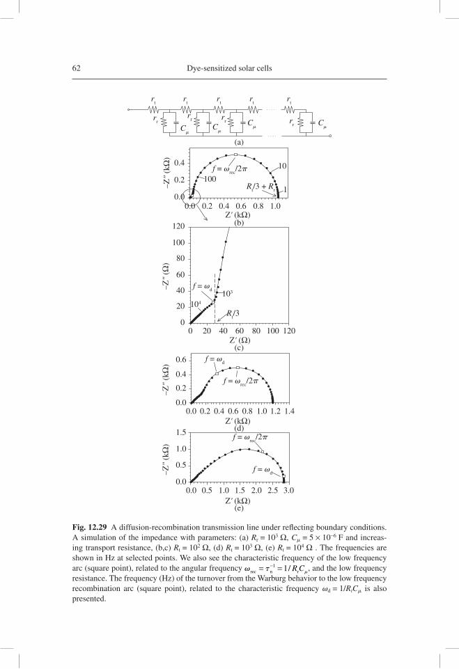
62 Dye-sensitized solar cells
Cm
Cm
Cm
Cm
rt
rt
rt
rt
rr
rrr
r rr
rt
0.4
100
10
1
f = vrec
/2p
Rt/3 + R
r
0.2
0.0
120
100
80
60
40
104
103
Rt/3
20
0
0.6
0.4
0.2
0.0
1.5
1.0
0.5
0.00.0 0.5 1.0 1.5 2.0 2.5 3.0
0.0 0.2 0.4 0.6 0.8 1.0 1.2 1.4
0 20 40 60 80 100 120
–Z"
(kΩ
)
Z' (kΩ)
Z' (kΩ)
–Z"
(Ω)
–Z"
(kΩ
)
Z' (kΩ)
–Z"
(kΩ
)
Z' (Ω)
0.0 0.2 0.4 0.6
(b)
(a)
(c)
(d)
(e)
0.8 1.0
f = vd
f = vd
f = vd
f = vrec
/2p
f = vrec
/2p
Fig. 12.29 A diffusion-recombination transmission line under refl ecting boundary conditions. A simulation of the impedance with parameters: (a) Rr = 103 Ω, Cm = 5 × 10⁻⁶ F and increas-ing transport resistance, (b,c) Rt = 102 Ω, (d) Rt = 103 Ω, (e) Rt = 104 Ω . The frequencies are shown in Hz at selected points. We also see the characteristic frequency of the low frequency arc (square point), related to the angular frequency vrec n r= =−
tm
1 1/ R C , and the low frequency resistance. The frequency (Hz) of the turnover from the Warburg behavior to the low frequency recombination arc (square point), related to the characteristic frequency vd = 1/RtCm is also presented.
Impedance spectroscopy 63
Figure 12.29 (b)-(c), corresponds to the carrier profi le (1) shown in Figure 12.28. This is the desired case for an effi cient DSC at moderate forward bias [12.65]. The oppo-site case, for strong recombination, i.e., for Rt > Rr, is shown in Figure 12.29(e), and relates to case (2) in Figure 12.28. The intermediate spectrum for Rt ≈ Rr is given in Figure 12.29(d).
The spectrum of Figure 12.29(b) has two features. At low frequency, there is a recombination arc, which is the parallel connection of Rr and Cm. The impedance at low frequency is given by the expression:
Z R
R= +
+1
3 tr
rec1 iv v/ (12.155)
The other feature is the diffusion Warburg, which is a small feature in the high frequency part of Figure 12.29(a), clearly visible in the enlarged plot of Figure 12.29(b), where we can see the start of the curvature of the capacitive part of Figure 12.27 due to recombination. As indicated in Eq. (12.155), we can in the spectrum of Figure 12.29(b) determine the electronic conductivity from Rt/3, i.e., the resistance at the turnover. This method has been effectively applied in various experi-ments [12.52, 12.65].
On the other hand, in the case of a strong recombination (vrec >> vd or Ln << L), the extent of penetration of the injected carriers in the layer, as well as the boundary condition, is irrelevant. The spectrum adopts the form of the Gerischer impedance,
ZR R
=⎛⎝⎜
⎞⎠⎟
t r
rec1 i+ v v/
/1 2
(12.156)
shown in Figure 12.29(e). When the carrier distribution is strongly inhomogene-ous, the chemical capacitance and recombination resistance depend on the position. Furthermore, additional current generators are required to correctly describe the impedance function [12.130].
12.6.4 Parameters of the diffusion-recombination model
Equation (12.153) is one way to express the diffusion-recombination impedance, but one can naturally also use other sets of parameters: the chemical capacitance, the chemical diffusion coeffi cient, etc. This may eventually lead to some confusion [12.64] and it is therefore important to establish very clearly what is the primary information that can be obtained from the impedance spectra. We recall that the recombination arc in Figure 12.29(b), is a fundamental requirement of a solar cell impedance model, as discussed before in Figure 12.13. However, the Warburg part in Figure 12.29(b) may or may not be observed. There are thus two basic situations.
The fi rst involves the case where the Warburg part is clearly observed at high fre-quency, in addition to the recombination arc. By “observed,” we mean that there is strong evidence that the spectra display this feature, although it may be hidden by other elements [12.137]. However, if the diffusion part is indeed detected, the impedance model provides three basic parameters: the recombination resistance Rr, the chemical capacitance Cm, and
64 Dye-sensitized solar cells
the transport resistance Rt. If the semiconductor shows a wide distribution of traps, the quasi-static approximation Eq. (12.153) is also valid. What we measure is however the total chemical capacitance that is dominated by Cm
traps , as discussed in Sec. 12.5.2. In any case, three independent impedance parameters can be derived from the model.
From these parameters we can additionally obtain:
(a) the electron conductivity, as discussed in Eqs. (12.144) and (12.145);
(b) the chemical diffusion coeffi cient, Dn,
DR C Ln = =1
2t
d
m
v (12.157)
This last equation corresponds to the generalized Einstein relation, s mn ntraps= D c ,
that was given in Eq. (12.120).
(c) the electron lifetime, given in Eq. (12.126), and which can be obtained as follows:
t mn r rec= = −R C v
1 (12.158)
We should further mention that for a “long” diffusion length, one can assume that transmission line elements are basically uniform. The macroscopic resistances and capacitance are thus simply related to the respective distributed TL elements by the fi lm dimensions. In the case of a strong recombination, on the other hand, simula-tion with spatially variable elements is generally required [12.130].
If, in addition, we have independent information regarding the position of the conduction band, we can also derive the free carrier diffusion coeffi cient and lifetime, using Eqs. (12.119) and (12.126).
Suppose now that the diffusion, i.e., the Warburg part of Figure 12.29(b), is not observed. We then have two independent impedance parameters: the recombination resistance Rr, and the trap-dominated chemical capacitance, Cm. There is no informa-tion at all regarding electron transport. In fact, the main reason why the Warburg part is undetected is that the conductivity is very high and transport resistance becomes extremely low. Consequently, the conductivity and chemical diffusion coeffi cient simply cannot be derived from the data in this case.
12.6.5 Effect of boundaries on the transmission line
So far, we have treated the impedance of diffusion with coupled processes, and with the condition of the refl ecting boundary at the end of the diffusion zone. Case (3) in Figure 12.28 shows a different situation. There occurs a strong recombination at the fi nal boundary, and the carriers must remain at the equilibrium level. The corresponding TL has a short-circuit at the end of the transport channel, as indicated in Figure 12.30. The impedance can be obtained from (12.140) with ZB = 0, and the result becomes:
Z R= ( ) ( )⎡
⎣⎤⎦
−t d di tanh iv v v v/ /
/ /1 2 1 2 (12.159)
Impedance spectroscopy 65
The impedance spectrum is shown in Figure 12.30. There is a diffusion Warburg part at high frequencies, but at low frequencies the impedance is obviously conductive through the transport channel. Eq. (12.159) also corresponds to diffusion between symmetric electrodes, and this renders it possible to determine the diffusion coef-fi cient of ions in viscous electrolytes for DSCs [12.66].
In Figure 12.13(c), we have presented a general comment of the effect of recombination at one boundary of the solar cell. We can now provide a more quan-titative picture of this effect by utilizing the TL model with a general boundary con-dition of Figure 12.25(b), described in Eq. (12.140). As an example, Figure 12.31 represents a DSC with a solid hole conductor, in which the more resistive transport channel is the organic conductor, so that the resistance of nanostructured TiO2 is set to 0. In the contact of the organic conductor with the substrate, there is a resistive/capacitive interface, describing the direct charge transfer through the substrate. This type of short-circuit must be avoided in DSCs, where the only transfer path should be the distributed interface of the TiO2/organic conductor. Figure 12.31(a) and (b) present simulations of the spectra with a variation of the charge transfer resistance at the substrate. In fact, the “shunt” resistance, RBL, at the substrate can be highly variable, since the potential in the substrate changes and one can expect a Butler-Volmer behavior [12.51]. When RBL is large, the substrate plays no role at all, and we obtain the spectrum of diffusion-reaction impedance shown in Figure 13.29(b). However, when RBL is below the bulk recombination resistance, the current fl ows predominantly through the substrate, and the TL model becomes similar to that of Figure 12.30. The observation of a transition from one type of spectrum to another may be useful in practice to determine the dominant resistance at each bias voltage.
0.5
0.5Z' (kΩ)
–Z"
(kΩ
)
1.0
f =vd
Rt
0.00.0
CmCm
rt
rt
rt
rt
rt
Cm Cm
(a)
(b)
Fig. 12.30 A representation of diffusion impedance of a fi lm of thickness L with an absorbing boundary. The characteristic frequency (Hz) of the turnover from the Warburg behavior to the low frequency arc (square point), related to the characteristic frequency vd = 1/RtCm is shown. Parameters Rt = 103 Ω, Cm = 1 × 10⁻³ F.
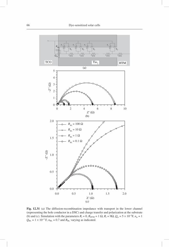
66 Dye-sensitized solar cells
RBL
rr
rr
rr
QBL
rHTM
qm
qm
qm
qm
rHTM
rHTM
rHTM
rHTM
rr
TCO Tio2 HTM
Z' (Ω)
–Z"
(Ω)
2 4 6 8 1000
1
2
3
4
5
RBL
= 100 Ω
RBL
= 10 Ω
RBL
= 1 Ω
RBL
= 0.1 Ω
0.0
2.0
1.5
1.0
0.5
0.0
0.5 1.0 1.5 2.0
Z' (Ω)
–Z"
(Ω)
(a)
(b)
(c)
Fig. 12.31 (a) The diffusion-recombination impedance with transport in the lower channel (representing the hole conductor in a DSC) and charge transfer and polarization at the substrate (b) and (c). Simulation with the parameters Rt = 0, RHTM = 1 Ω, Rr = 9Ω, Qm = 5 × 10⁻³F, nm = 1 QBL = 1 × 10⁻² F, nBL = 0.7 and RBL varying as indicated.
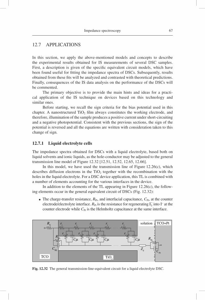
Impedance spectroscopy 67
12.7 APPLICATIONS
In this section, we apply the above-mentioned models and concepts to describe the experimental results obtained for IS measurements of several DSC samples. First, a description is given of the specifi c equivalent circuit models, which have been found useful for fi tting the impedance spectra of DSCs. Subsequently, results obtained from these fi ts will be analyzed and contrasted with theoretical predictions. Finally, consequences of the IS data analysis on the performance of the DSCs will be commented.
The primary objective is to provide the main hints and ideas for a practi-cal application of the IS technique on devices based on this technology and similar ones.
Before starting, we recall the sign criteria for the bias potential used in this chapter. A nanostructured TiO2 fi lm always constitutes the working electrode, and therefore, illumination of the sample produces a positive current under short-circuiting and a negative photopotential. Consistent with the previous sections, the sign of the potential is reversed and all the equations are written with consideration taken to this change of sign.
12.7.1 Liquid electrolyte cells
The impedance spectra obtained for DSCs with a liquid electrolyte, based both on liquid solvents and ionic liquids, as the hole-conductor may be adjusted to the general transmission line model of Figure 12.32 [12.51, 12.52, 12.65, 12.66].
In this model, we have used the transmission line of Figure 12.26(c), which describes diffusion electrons in the TiO2 together with the recombination with the holes in the liquid electrolyte. For a DSC device application, this TL is combined with a number of elements accounting for the various interfaces in the device.
In addition to the elements of the TL appearing in Figure 12.26(c), the follow-ing elements occur in the general equivalent circuit of DSCs (Fig. 12.32):
● The charge-transfer resistance, RPt, and interfacial capacitance, CPt, at the counter electrode/electrolyte interface. RPt is the resistance for regenerating I3
− into I− at the counter electrode while CPt is the Helmholtz capacitance at the same interface.
TCO
RS
CBL
RBL
rt
rr
rr
rr
rr
rt
rt
rt
rt
TiO2
TCO+Ptsolution
Cm Cm Cm Cm RPt
CPt
Zd
Fig. 12.32 The general transmission-line-equivalent circuit for a liquid electrolyte DSC.
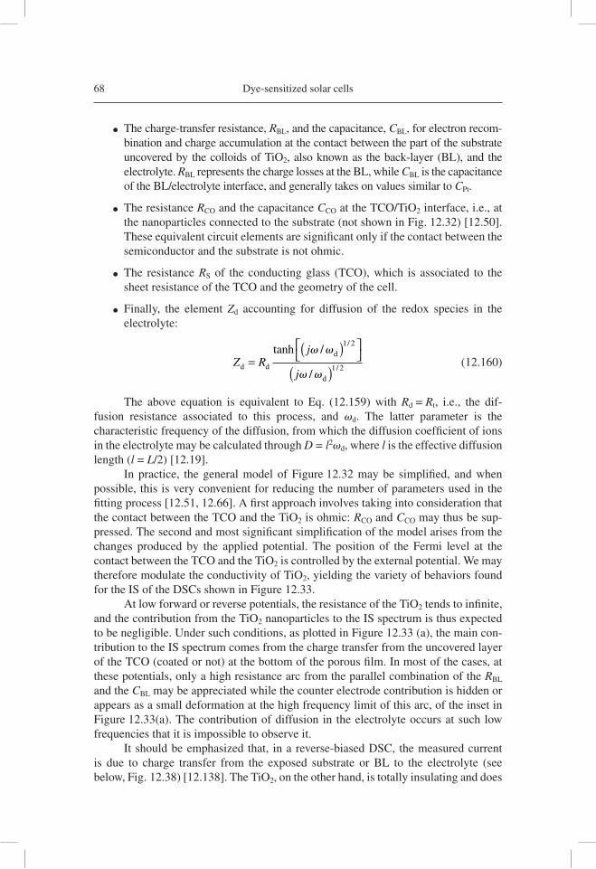
68 Dye-sensitized solar cells
● The charge-transfer resistance, RBL, and the capacitance, CBL, for electron recom-bination and charge accumulation at the contact between the part of the substrate uncovered by the colloids of TiO2, also known as the back-layer (BL), and the electrolyte. RBL represents the charge losses at the BL, while CBL is the capacitance of the BL/electrolyte interface, and generally takes on values similar to CPt.
● The resistance RCO and the capacitance CCO at the TCO/TiO2 interface, i.e., at the nanoparticles connected to the substrate (not shown in Fig. 12.32) [12.50]. These equivalent circuit elements are signifi cant only if the contact between the semiconductor and the substrate is not ohmic.
● The resistance RS of the conducting glass (TCO), which is associated to the sheet resistance of the TCO and the geometry of the cell.
● Finally, the element Zd accounting for diffusion of the redox species in the electrolyte:
Z Rj
jd d
d
d
=( )⎡
⎣⎤⎦
( )tanh /
/
/
/
v v
v v
1 2
1 2 (12.160)
The above equation is equivalent to Eq. (12.159) with Rd = Rt, i.e., the dif-fusion resistance associated to this process, and vd. The latter parameter is the characteristic frequency of the diffusion, from which the diffusion coeffi cient of ions in the electrolyte may be calculated through D = l2vd, where l is the effective diffusion length (l = L/2) [12.19].
In practice, the general model of Figure 12.32 may be simplifi ed, and when possible, this is very convenient for reducing the number of parameters used in the fi tting process [12.51, 12.66]. A fi rst approach involves taking into consideration that the contact between the TCO and the TiO2 is ohmic: RCO and CCO may thus be sup-pressed. The second and most signifi cant simplifi cation of the model arises from the changes produced by the applied potential. The position of the Fermi level at the contact between the TCO and the TiO2 is controlled by the external potential. We may therefore modulate the conductivity of TiO2, yielding the variety of behaviors found for the IS of the DSCs shown in Figure 12.33.
At low forward or reverse potentials, the resistance of the TiO2 tends to infi nite, and the contribution from the TiO2 nanoparticles to the IS spectrum is thus expected to be negligible. Under such conditions, as plotted in Figure 12.33 (a), the main con-tribution to the IS spectrum comes from the charge transfer from the uncovered layer of the TCO (coated or not) at the bottom of the porous fi lm. In most of the cases, at these potentials, only a high resistance arc from the parallel combination of the RBL and the CBL may be appreciated while the counter electrode contribution is hidden or appears as a small deformation at the high frequency limit of this arc, of the inset in Figure 12.33(a). The contribution of diffusion in the electrolyte occurs at such low frequencies that it is impossible to observe it.
It should be emphasized that, in a reverse-biased DSC, the measured current is due to charge transfer from the exposed substrate or BL to the electrolyte (see below, Fig. 12.38) [12.138]. The TiO2, on the other hand, is totally insulating and does
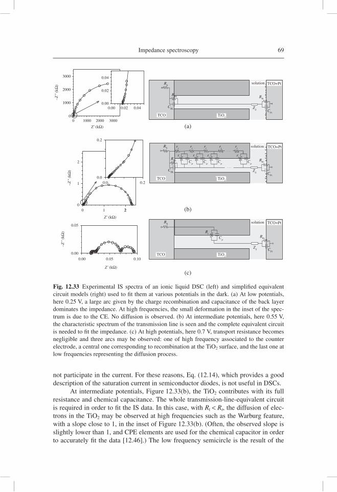
Impedance spectroscopy 69
not participate in the current. For these reasons, Eq. (12.14), which provides a good description of the saturation current in semiconductor diodes, is not useful in DSCs.
At intermediate potentials, Figure 12.33(b), the TiO2 contributes with its full resistance and chemical capacitance. The whole transmission-line-equivalent circuit is required in order to fi t the IS data. In this case, with Rt < Rr, the diffusion of elec-trons in the TiO2 may be observed at high frequencies such as the Warburg feature, with a slope close to 1, in the inset of Figure 12.33(b). (Often, the observed slope is slightly lower than 1, and CPE elements are used for the chemical capacitor in order to accurately fi t the data [12.46].) The low frequency semicircle is the result of the
3000 0.04
0.02
0.000.00 0.02 0.04
2000
1000
–Z"
(kΩ
)
Z' (kΩ) (a)
(b)
(c)
00 1000 2000 3000
RS
RBL R
Pt
Zd C
Pt
CBL
TCO TiO2
solution TCO+Pt
TCO TiO2
solution TCO+Pt
TCO TiO2
solution TCO+Pt
2
0.2
0.00.0 0.21
00 1 22
–Z"
(kΩ
)
Z' (kΩ)
RS r
tr
tr
tr
tr
t
Zd
RPt
CPt
rr
rr
Cm
Cm
Cm
Cm
rr
rrR
BL
CBL
RS
Rr
Zd
RPt
CPt
Cm
0.05
0.000.00 0.05 0.10
–Z"
(kΩ
)
Z' (kΩ)
Fig. 12.33 Experimental IS spectra of an ionic liquid DSC (left) and simplifi ed equivalent circuit models (right) used to fi t them at various potentials in the dark. (a) At low potentials, here 0.25 V, a large arc given by the charge recombination and capacitance of the back layer dominates the impedance. At high frequencies, the small deformation in the inset of the spec-trum is due to the CE. No diffusion is observed. (b) At intermediate potentials, here 0.55 V, the characteristic spectrum of the transmission line is seen and the complete equivalent circuit is needed to fi t the impedance. (c) At high potentials, here 0.7 V, transport resistance becomes negligible and three arcs may be observed: one of high frequency associated to the counter electrode, a central one corresponding to recombination at the TiO2 surface, and the last one at low frequencies representing the diffusion process.
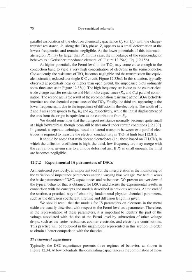
70 Dye-sensitized solar cells
parallel association of the electron chemical capacitance Cm (or Qm) with the charge-transfer resistance, Rr, along the TiO2 phase. Zd appears as a small deformation at the lowest frequencies and remains negligible. At the lower potentials of this intermedi-ate region, Rt may be larger than Rr. In this case, the impedance of the semiconductor behaves as a Gerischer impedance element, cf. Figure 12.29(e), Eq. (12.156).
At higher potentials, the Fermi level in the TiO2 may come close enough to the conduction band to yield a very high concentration of electrons in the semiconductor. Consequently, the resistance of TiO2 becomes negligible and the transmission line equiv-alent circuit is reduced to a single R-C circuit, Figure 12.33(c). In this situation, typically observed at potentials near or higher than open circuit, the impedance plots ordinarily show three arcs as in Figure 12.33(c). The high frequency arc is due to the counter-elec-trode charge transfer resistance and Helmholtz capacitance (RPt and CPt) parallel combi-nation. The second arc is the result of the recombination resistance at the TiO2/electrolyte interface and the chemical capacitance of the TiO2. Finally, the third arc, appearing at the lower frequencies, is due to the impedance of diffusion in the electrolyte. The width of 1, 2 and 3 arcs corresponds to RPt, Rct and Rd, respectively, while the initial displacement of the arcs from the origin is equivalent to the contribution from RS.
We should remember that the transport resistance normally becomes quite small at a high forward bias, though it can still be measured under certain conditions [12.139]. In general, a separate technique based on lateral transport between two parallel elec-trodes is required to measure the electron conductivity in TiO2 at high bias [12.81].
It should be noted that with decent electrolytes (i.e., those based on CH3CN), in which the diffusion coeffi cient is high, the third, low-frequency arc may merge with the central one, giving rise to a unique deformed arc. If Rd is small enough, the third arc becomes negligible.
12.7.2 Experimental IS parameters of DSCs
As mentioned previously, an important tool for the interpretation is the monitoring of the variation of impedance parameters under a varying bias voltage. We here discuss the basic parameters of DSC, capacitances and resistances. We present an overview of the typical behavior that is obtained for DSCs and discuss the experimental results in connection with the concepts and models described in previous sections. At the end of the section, a practical way of obtaining fundamental physico-chemical parameters, such as the diffusion coeffi cient, lifetime and diffusion length, is given.
We should recall that the models for IS parameters on electrons in the metal oxide are usually described with respect to the Fermi level as a parameter. Therefore, in the representation of these parameters, it is important to identify the part of the voltage associated with the rise of the Fermi level by subtraction of other voltage drops, such as the series resistance, counter electrode, and electrolyte contributions. This practice will be followed in the magnitudes represented in this section, in order to obtain a better comparison with the theories.
The chemical capacitance
Typically, the DSC capacitance presents three regimes of behavior, as shown in Figure 12.34. At low potentials, the dominating capacitance is the combination of those
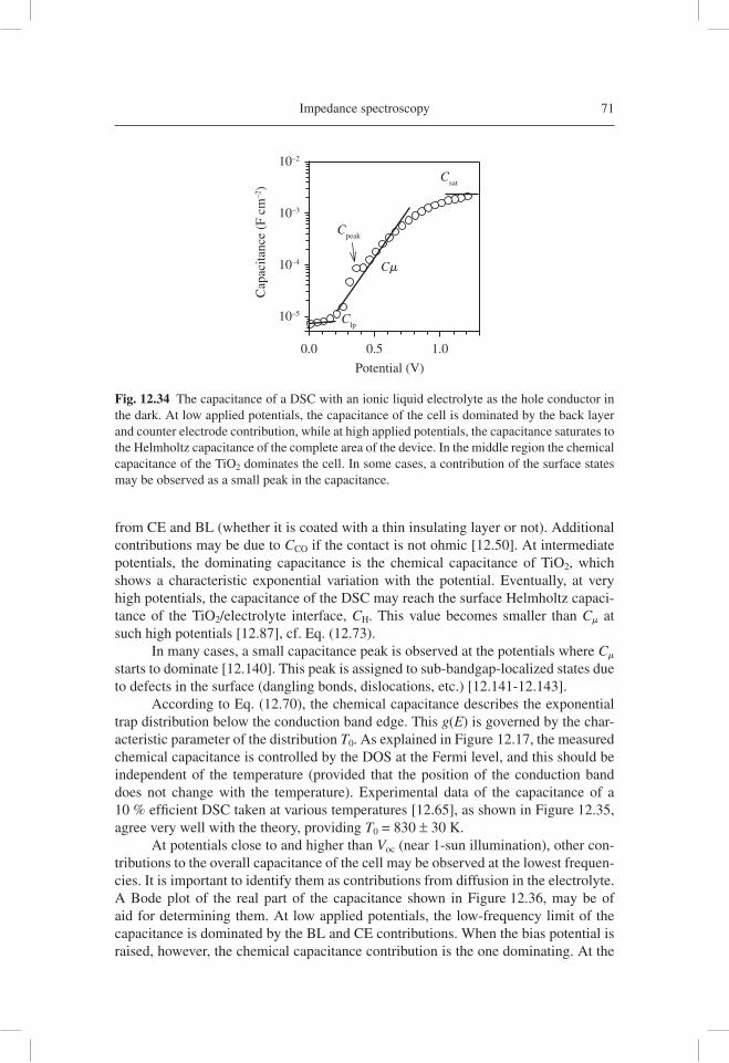
Impedance spectroscopy 71
from CE and BL (whether it is coated with a thin insulating layer or not). Additional contributions may be due to CCO if the contact is not ohmic [12.50]. At intermediate potentials, the dominating capacitance is the chemical capacitance of TiO2, which shows a characteristic exponential variation with the potential. Eventually, at very high potentials, the capacitance of the DSC may reach the surface Helmholtz capaci-tance of the TiO2/electrolyte interface, CH. This value becomes smaller than Cm at such high potentials [12.87], cf. Eq. (12.73).
In many cases, a small capacitance peak is observed at the potentials where Cm starts to dominate [12.140]. This peak is assigned to sub-bandgap-localized states due to defects in the surface (dangling bonds, dislocations, etc.) [12.141-12.143].
According to Eq. (12.70), the chemical capacitance describes the exponential trap distribution below the conduction band edge. This g(E) is governed by the char-acteristic parameter of the distribution T0. As explained in Figure 12.17, the measured chemical capacitance is controlled by the DOS at the Fermi level, and this should be independent of the temperature (provided that the position of the conduction band does not change with the temperature). Experimental data of the capacitance of a 10 % effi cient DSC taken at various temperatures [12.65], as shown in Figure 12.35, agree very well with the theory, providing T0 = 830 ± 30 K.
At potentials close to and higher than Voc (near 1-sun illumination), other con-tributions to the overall capacitance of the cell may be observed at the lowest frequen-cies. It is important to identify them as contributions from diffusion in the electrolyte. A Bode plot of the real part of the capacitance shown in Figure 12.36, may be of aid for determining them. At low applied potentials, the low-frequency limit of the capacitance is dominated by the BL and CE contributions. When the bias potential is raised, however, the chemical capacitance contribution is the one dominating. At the
Potential (V)
Cap
acita
nce
(F c
m–2
)
0.0
10–5
10–4
10–3
10–2
0.5
Clp
Cpeak
Csat
1.0
Cm
Fig. 12.34 The capacitance of a DSC with an ionic liquid electrolyte as the hole conductor in the dark. At low applied potentials, the capacitance of the cell is dominated by the back layer and counter electrode contribution, while at high applied potentials, the capacitance saturates to the Helmholtz capacitance of the complete area of the device. In the middle region the chemical capacitance of the TiO2 dominates the cell. In some cases, a contribution of the surface states may be observed as a small peak in the capacitance.
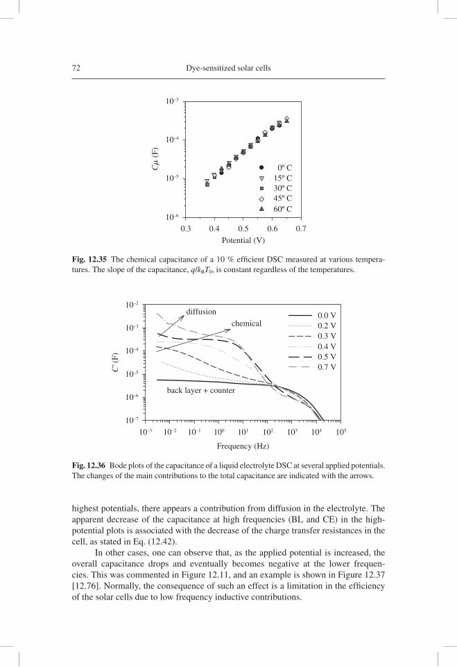
72 Dye-sensitized solar cells
highest potentials, there appears a contribution from diffusion in the electrolyte. The apparent decrease of the capacitance at high frequencies (BL and CE) in the high-potential plots is associated with the decrease of the charge transfer resistances in the cell, as stated in Eq. (12.42).
In other cases, one can observe that, as the applied potential is increased, the overall capacitance drops and eventually becomes negative at the lower frequen-cies. This was commented in Figure 12.11, and an example is shown in Figure 12.37 [12.76]. Normally, the consequence of such an effect is a limitation in the effi ciency of the solar cells due to low frequency inductive contributions.
10–2
diffusion
chemical0.0 V0.2 V0.3 V0.4 V0.5 V0.7 V
10–3
10–4
10–5
10–6
10–7
10–3 10–2 10–1 100 101
Frequency (Hz)
back layer + counter
C' (
F)
102 103 104 105
Fig. 12.36 Bode plots of the capacitance of a liquid electrolyte DSC at several applied potentials. The changes of the main contributions to the total capacitance are indicated with the arrows.
10–3
10–4
10–5
10–6
0.3
Cm
(F)
0.4 0.5
Potential (V)
0.6 0.7
0º C15º C30º C45º C60º C
Fig. 12.35 The chemical capacitance of a 10 % effi cient DSC measured at various tempera-tures. The slope of the capacitance, q/kBT0, is constant regardless of the temperatures.
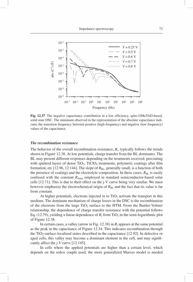
Impedance spectroscopy 73
The recombination resistance
The behavior of the overall recombination resistance, Rr, typically follows the trends shown in Figure 12.38. At low potentials, charge transfer from the BL dominates. The BL may present different responses depending on the treatments received: precoating with sputterd layers of dense TiO2, TiClO4 treatments, polymeric coatings after fi lm formation, etc [12.96, 12.144]. The slope of RBL, generally small, is a function of both the presence of coatings and the electrolyte composition. In these cases, RBL is easily confused with the constant Rshunt employed in standard semiconductor-based solar cells [12.71]. This is due to their effect on the j-V curve being very similar. We must however emphasize the electrochemical origin of RBL and the fact that its value is far from constant.
At higher potentials, electrons injected in to TiO2 activate the transport in this medium. The dominant mechanism of charge losses in the DSC is the recombination of the electrons from the large TiO2 surface to the HTM. From the Buttler-Volmer relationship, the dependence of charge transfer resistance with the potential follows Eq. (12.79), yielding a linear dependence of Rr from TiO2 in the semi-logarithmic plot of Figure 12.38.
In certain cases, a valley (arrow in Fig. 12.38) in Rr appears at the same potential as the peak in the capacitance of Figure 12.34. This indicates recombination through the TiO2-surface-localized states described in the capacitance [12.92]. In defective or aged cells, this valley may become a dominant element in the cell, and may signifi -cantly affect the j-V curve [12.145].
In cells where the applied potentials are higher than a certain level, which depends on the redox couple used, the more generalized Marcus model is needed
10–2
V = 0.25 VV = 0.5 VV = 0.6 VV = 0.7 VV = 0.8 V
10–3
10–3 10–2 10–1 100 101
Frequency (Hz)
abs
(C')
(F)
102 103 104 105 106
10–4
10–5
10–6
10–7
10–8
10–9
Fig. 12.37 The negative capacitance contribution in a low effi ciency, spiro-OMeTAD-based, solid state DSC. The minimum observed in the representation of the absolute capacitance indi-cates the transition frequency between positive (high frequency) and negative (low frequency) values of the capacitance.
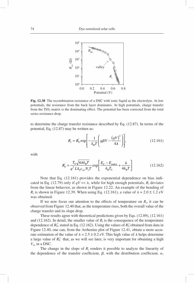
74 Dye-sensitized solar cells
to determine the charge transfer resistance described by Eq. (12.87). In terms of the potential, Eq. (12.87) may be written as:
R Rk T
q VqV
rB
= − − ( )⎛
⎝⎜
⎞
⎠⎟
⎡
⎣⎢⎢
⎤
⎦⎥⎥0
21
4′ exp ,b
l (12.161)
with
RT k T
q Lk c N T
E E
k T k T00
20 0 4
′ =−
+⎡
⎣⎢
⎤
⎦⎥
πl lB
ox s
C redox
B B
exp (12.162)
Note that Eq. (12.161) provides the exponential dependence on bias indi-cated in Eq. (12.79) only if qV << l, while for high enough potentials, Rr deviates from the linear behavior, as shown in Figure 12.22. An example of the bending of Rr is shown in Figure 12.39. When using Eq. (12.161), a value of l = 2.0 ± 1.2 eV was obtained.
If we now focus our attention to the effects of temperature on Rr, it can be observed from Figure 12.40 that, as the temperature rises, both the overall value of the charge transfer and its slope drop.
These results agree with theoretical predictions given by Eqs. (12.89), (12.161) and (12.162). In detail, the smaller value of Rr is the consequence of the temperature dependence of R0′, stated in Eq. (12.162). Using the values of R0′ obtained from data in Figure 12.40, one can, from the Arrhenius plot of Figure 12.41, obtain a more accu-rate estimation of the value of l = 2.5 ± 0.2 eV. This high value of l helps determine a large value of R0′ that, as we will see later, is very important for obtaining a high Voc in a DSC.
The change in the slope of Rr renders it possible to analyze the linearity of the dependence of the transfer coeffi cient, b, with the distribution coeffi cient, a,
105
104
103
102
101
100
0.0 0.2 0.4Potential (V)
valleyRre
c (Ω
)
RBL
Rr
0.6 0.8
Fig. 12.38 The recombination resistance of a DSC with ionic liquid as the electrolyte. At low potentials, the resistance from the back layer dominates. At high potentials, charge transfer from the TiO2 matrix is the dominating effect. The potential has been corrected from the total series resistance drop.
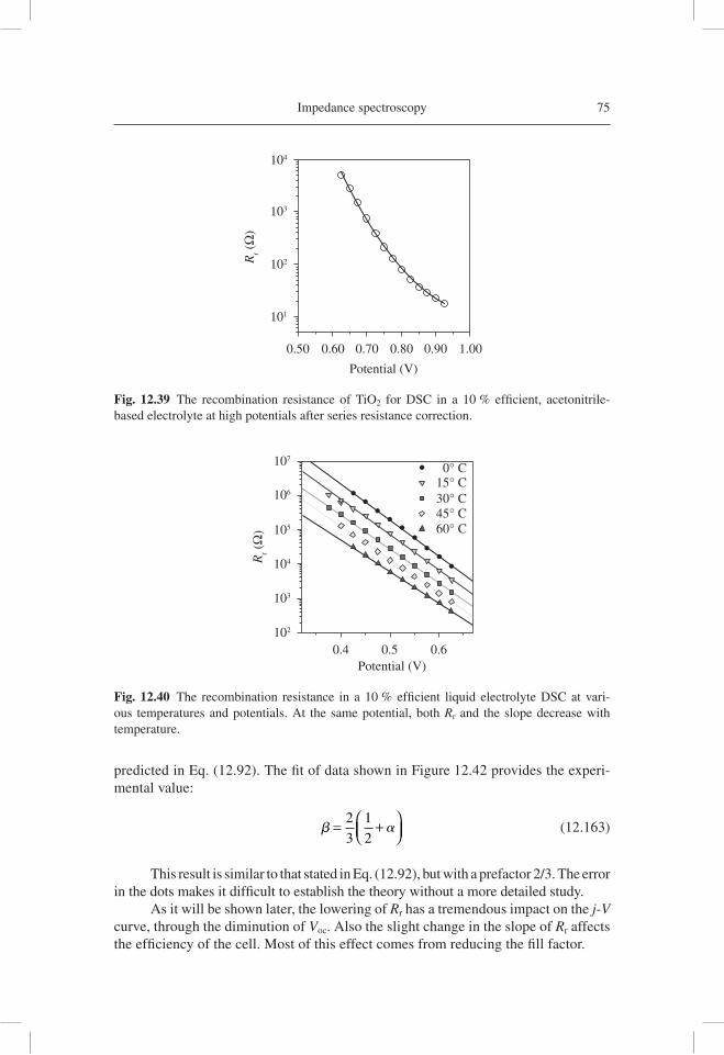
Impedance spectroscopy 75
104
103
102
101
0.50 0.60 0.70
Potential (V)
Rr (
Ω)
0.80 0.90 1.00
Fig. 12.39 The recombination resistance of TiO2 for DSC in a 10 % effi cient, acetonitrile-based electrolyte at high potentials after series resistance correction.
107
0° C15° C30° C45° C60° C
106
105
104
103
102
0.4 0.5Potential (V)
Rr (
Ω)
0.6
Fig. 12.40 The recombination resistance in a 10 % effi cient liquid electrolyte DSC at vari-ous temperatures and potentials. At the same potential, both Rr and the slope decrease with temperature.
predicted in Eq. (12.92). The fi t of data shown in Figure 12.42 provides the experi-mental value:
b a= +⎛
⎝⎜⎞⎠⎟
2
3
1
2 (12.163)
This result is similar to that stated in Eq. (12.92), but with a prefactor 2/3. The error in the dots makes it diffi cult to establish the theory without a more detailed study.
As it will be shown later, the lowering of Rr has a tremendous impact on the j-V curve, through the diminution of Voc. Also the slight change in the slope of Rr affects the effi ciency of the cell. Most of this effect comes from reducing the fi ll factor.
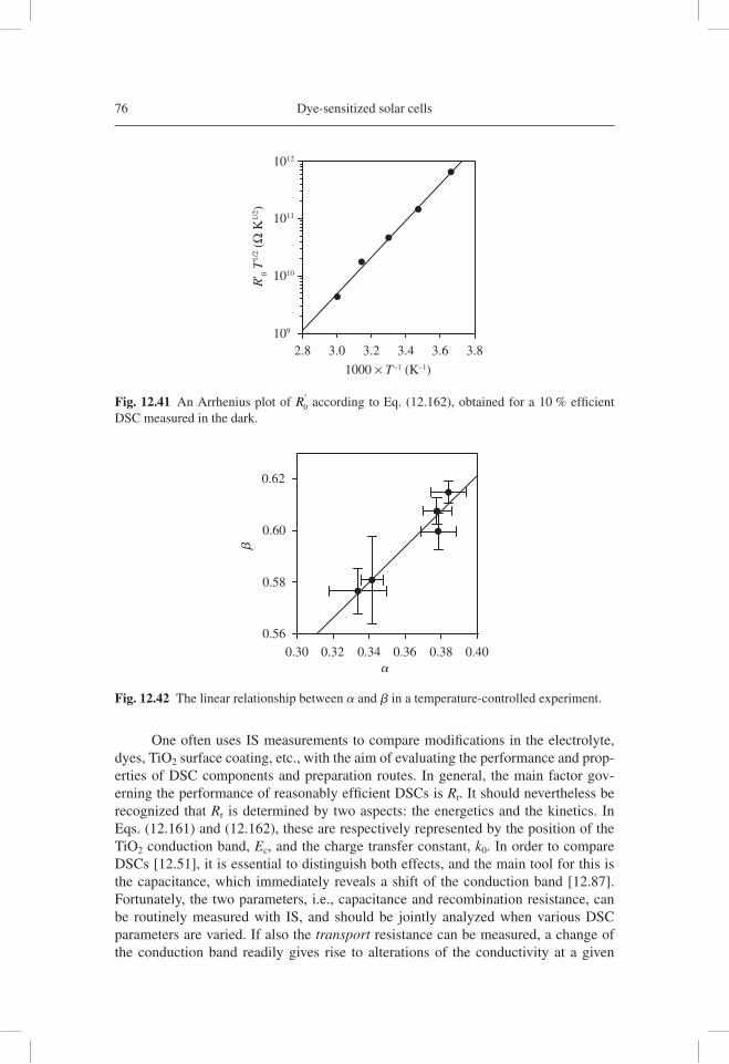
76 Dye-sensitized solar cells
One often uses IS measurements to compare modifi cations in the electrolyte, dyes, TiO2 surface coating, etc., with the aim of evaluating the performance and prop-erties of DSC components and preparation routes. In general, the main factor gov-erning the performance of reasonably effi cient DSCs is Rr. It should nevertheless be recognized that Rr is determined by two aspects: the energetics and the kinetics. In Eqs. (12.161) and (12.162), these are respectively represented by the position of the TiO2 conduction band, Ec, and the charge transfer constant, k0. In order to compare DSCs [12.51], it is essential to distinguish both effects, and the main tool for this is the capacitance, which immediately reveals a shift of the conduction band [12.87]. Fortunately, the two parameters, i.e., capacitance and recombination resistance, can be routinely measured with IS, and should be jointly analyzed when various DSC parameters are varied. If also the transport resistance can be measured, a change of the conduction band readily gives rise to alterations of the conductivity at a given
b
a
0.340.320.300.56
0.58
0.60
0.62
0.36 0.38 0.40
Fig. 12.42 The linear relationship between a and b in a temperature-controlled experiment.
1012
1011
1010
109
1000 × T–1 (K–1)
R' 0 T
1/2 (
Ω K
1/2 )
2.8 3.0 3.2 3.4 3.6 3.8
Fig. 12.41 An Arrhenius plot of R0′ according to Eq. (12.162), obtained for a 10 % effi cient
DSC measured in the dark.
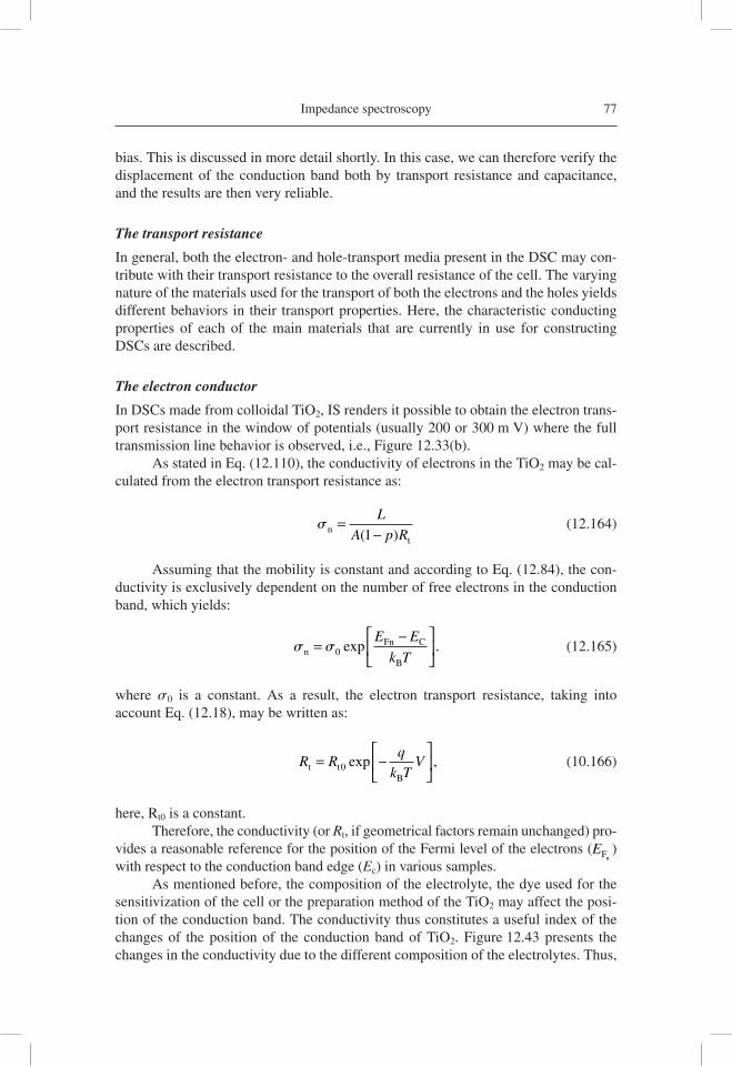
Impedance spectroscopy 77
bias. This is discussed in more detail shortly. In this case, we can therefore verify the displacement of the conduction band both by transport resistance and capacitance, and the results are then very reliable.
The transport resistance
In general, both the electron- and hole-transport media present in the DSC may con-tribute with their transport resistance to the overall resistance of the cell. The varying nature of the materials used for the transport of both the electrons and the holes yields different behaviors in their transport properties. Here, the characteristic conducting properties of each of the main materials that are currently in use for constructing DSCs are described.
The electron conductor
In DSCs made from colloidal TiO2, IS renders it possible to obtain the electron trans-port resistance in the window of potentials (usually 200 or 300 m V) where the full transmission line behavior is observed, i.e., Figure 12.33(b).
As stated in Eq. (12.110), the conductivity of electrons in the TiO2 may be cal-culated from the electron transport resistance as:
sn
t
=−L
A p R( )1 (12.164)
Assuming that the mobility is constant and according to Eq. (12.84), the con-ductivity is exclusively dependent on the number of free electrons in the conduction band, which yields:
s snFn C
B
=−⎡
⎣⎢
⎤
⎦⎥0 exp .
E E
k T (12.165)
where s0 is a constant. As a result, the electron transport resistance, taking into account Eq. (12.18), may be written as:
R Rq
k TVt t
B
= −⎡
⎣⎢
⎤
⎦⎥0 exp , (10.166)
here, Rt0 is a constant.Therefore, the conductivity (or Rt, if geometrical factors remain unchanged) pro-
vides a reasonable reference for the position of the Fermi level of the electrons (EFn)
with respect to the conduction band edge (Ec) in various samples.As mentioned before, the composition of the electrolyte, the dye used for the
sensitivization of the cell or the preparation method of the TiO2 may affect the posi-tion of the conduction band. The conductivity thus constitutes a useful index of the changes of the position of the conduction band of TiO2. Figure 12.43 presents the changes in the conductivity due to the different composition of the electrolytes. Thus,
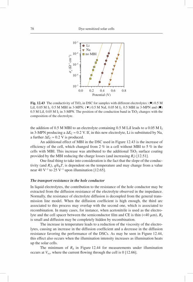
78 Dye-sensitized solar cells
the addition of 0.5 M MBI to an electrolyte containing 0.5 M LiI leads to a 0.05 M I2 in 3-MPN producing a ΔEC ≈ 0.2 V. If, in this new electrolyte, Li is substituted by Na, a further ΔEC ≈ 0.2 V is produced.
An additional effect of MBI in the DSC used in Figure 12.43 is the increase of effi ciency of the cell, which changed from 2 % in a cell without MBI to 5 % in the cells with MBI. This increase was attributed to the additional TiO2 surface coating provided by the MBI reducing the charge losses (and increasing Rr) [12.51].
One fi nal thing to take into consideration is the fact that the slope of the conduc-tivity (and Rt), q/kBT, is dependent on the temperature and may change from a value near 40 V−1 to 25 V−1 upon illumination [12.65].
The transport resistance in the hole conductor
In liquid electrolytes, the contribution to the resistance of the hole conductor may be extracted from the diffusion resistance of the electrolyte observed in the impedance. Normally, the resistance of electrolyte diffusion is decoupled from the general trans-mission line model. When the diffusion coeffi cient is high enough, the third arc associated to this process may overlap with the second one, which is associated to recombination. In many cases, for instance, when acetonitrile is used as the electro-lyte and the cell spacer between the semiconductor fi lm and CE is thin (<40 mm), Rd is small and diffusion may be completely hidden by recombination.
The increase in temperature leads to a reduction of the viscosity of the electro-lytes, causing an increase in the diffusion coeffi cient and a decrease in the diffusion resistance favoring the performance of the DSCs. As may be seen in Figure 12.44, this effect also occurs when the illumination intensity increases as illumination heats up the solar cells.
The minimum of Rd in Figure 12.44 for measurements under illumination occurs at Voc, where the current fl owing through the cell is 0 [12.66].
0.2Potential (V)
sn (
Ω–1
cm
–1)
0.010–7
10–6
10–5
10–4
LiNano MBI
10–3
0.4 0.6 0.8
Fig. 12.43 The conductivity of TiO2 in DSC for samples with different electrolytes: ( ) 0.5 M LiI, 0.05 M I2, 0.5 M MBI in 3-MPN; ( ) 0.5 M NaI, 0.05 M I2, 0.5 MBI in 3-MPN and ( ) 0.5 M LiI, 0.05 M I2 in 3-MPN. The position of the conduction band in TiO2 changes with the composition of the electrolyte.
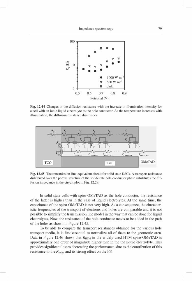
Impedance spectroscopy 79
In solid state cells with spiro-OMeTAD as the hole conductor, the resistance of the latter is higher than in the case of liquid electrolytes. At the same time, the capacitance of the spiro-OMeTAD is not very high. As a consequence, the character-istic frequencies of the transport of electrons and holes are comparable and it is not possible to simplify the transmission line model in the way that can be done for liquid electrolytes. Now, the resistance of the hole conductor needs to be added in the path of the holes as shown in Figure 12.45.
To be able to compare the transport resistances obtained for the various hole transport media, it is fi rst essential to normalize all of them to the geometric area. Data in Figure 12.46 shows that RHTM in the widely used HTM spiro-OMeTAD is approximately one order of magnitude higher than in the the liquid electrolyte. This provides signifi cant losses decreasing the performance, due to the contribution of this resistance to the Rseries and its strong effect on the FF.
1
10
100
Potential (V)
Rd (
Ω)
dark500 W m–2
1000 W m–2
0.60.5 0.7 0.8 0.9
Fig. 12.44 Changes in the diffusion resistance with the increase in illumination intensity for a cell with an ionic liquid electrolyte as the hole conductor. As the temperature increases with illumination, the diffusion resistance diminishes.
Cm
Cm
Cm
Cm
RS
RBL
CBL r
OMeTADr
OMeTADr
OMeTADr
OMeTADr
OMeTAD
rt
rt
rt
rt
rt
rt
rt
rt
rt
OMeTADTiO2
TCO
Fig. 12.45 The transmission-line-equivalent circuit for solid state DSCs. A transport resistance distributed over the porous structure of the solid-state hole conductor phase substitutes the dif-fusion impedance in the circuit plot in Fig. 12.29.
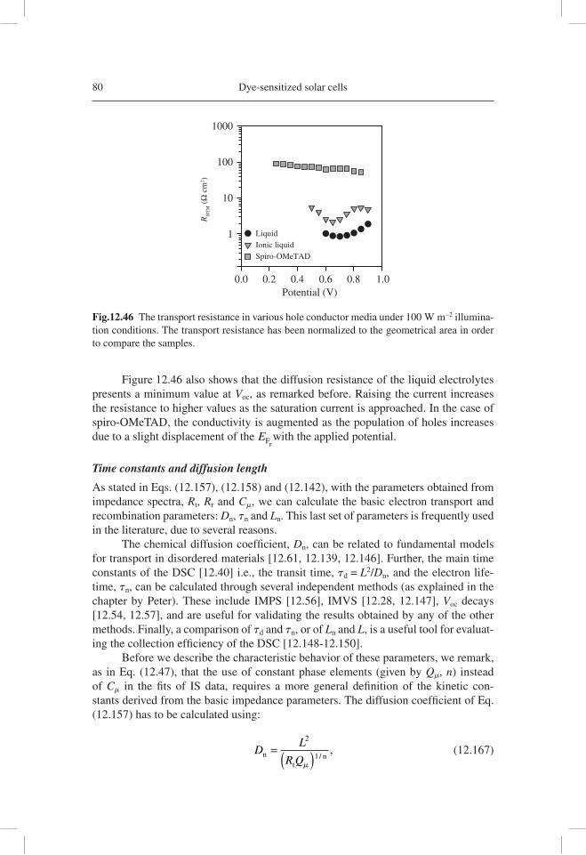
80 Dye-sensitized solar cells
Figure 12.46 also shows that the diffusion resistance of the liquid electrolytes presents a minimum value at Voc, as remarked before. Raising the current increases the resistance to higher values as the saturation current is approached. In the case of spiro-OMeTAD, the conductivity is augmented as the population of holes increases due to a slight displacement of the EFp
with the applied potential.
Time constants and diffusion length
As stated in Eqs. (12.157), (12.158) and (12.142), with the parameters obtained from impedance spectra, Rt, Rr and Cm, we can calculate the basic electron transport and recombination parameters: Dn, tn and Ln. This last set of parameters is frequently used in the literature, due to several reasons.
The chemical diffusion coeffi cient, Dn, can be related to fundamental models for transport in disordered materials [12.61, 12.139, 12.146]. Further, the main time constants of the DSC [12.40] i.e., the transit time, td = L2/Dn, and the electron life-time, tn, can be calculated through several independent methods (as explained in the chapter by Peter). These include IMPS [12.56], IMVS [12.28, 12.147], Voc decays [12.54, 12.57], and are useful for validating the results obtained by any of the other methods. Finally, a comparison of td and tn, or of Ln and L, is a useful tool for evaluat-ing the collection effi ciency of the DSC [12.148-12.150].
Before we describe the characteristic behavior of these parameters, we remark, as in Eq. (12.47), that the use of constant phase elements (given by Qm, n) instead of Cm in the fi ts of IS data, requires a more general defi nition of the kinetic con-stants derived from the basic impedance parameters. The diffusion coeffi cient of Eq. (12.157) has to be calculated using:
DL
R Qn
tn
= ( )2
1m
/, (12.167)
1
10
100
1000
Potential (V)0.0 0.2 0.4 0.6 0.8 1.0
Liquid
RH
TM
(Ω
cm
2 )
Ionic liquidSpiro-OMeTAD
Fig.12.46 The transport resistance in various hole conductor media under 100 W m−2 illumina-tion conditions. The transport resistance has been normalized to the geometrical area in order to compare the samples.
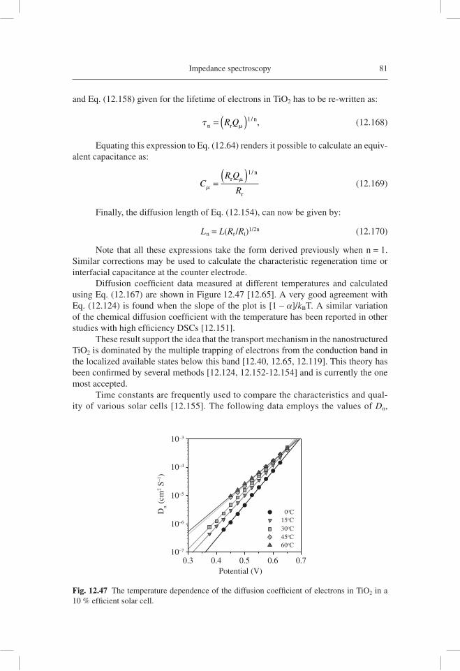
Impedance spectroscopy 81
and Eq. (12.158) given for the lifetime of electrons in TiO2 has to be re-written as:
t mn r
n= ( )R Q 1/ , (12.168)
Equating this expression to Eq. (12.64) renders it possible to calculate an equiv-alent capacitance as:
C
R Q
Rm
m=( )r
n
r
1/
(12.169)
Finally, the diffusion length of Eq. (12.154), can now be given by:
Ln = L(Rr/Rt)1/2n (12.170)
Note that all these expressions take the form derived previously when n = 1. Similar corrections may be used to calculate the characteristic regeneration time or interfacial capacitance at the counter electrode.
Diffusion coeffi cient data measured at different temperatures and calculated using Eq. (12.167) are shown in Figure 12.47 [12.65]. A very good agreement with Eq. (12.124) is found when the slope of the plot is [1 − a]/kBT. A similar variation of the chemical diffusion coeffi cient with the temperature has been reported in other studies with high effi ciency DSCs [12.151].
These result support the idea that the transport mechanism in the nanostructured TiO2 is dominated by the multiple trapping of electrons from the conduction band in the localized available states below this band [12.40, 12.65, 12.119]. This theory has been confi rmed by several methods [12.124, 12.152-12.154] and is currently the one most accepted.
Time constants are frequently used to compare the characteristics and qual-ity of various solar cells [12.155]. The following data employs the values of Dn,
Potential (V)
Dn (
cm2 S
–1)
0.5 0.6 0.70.40.310–7
10–6
10–5
10–4
10–3
0oC15oC30oC45oC60oC
Fig. 12.47 The temperature dependence of the diffusion coeffi cient of electrons in TiO2 in a 10 % effi cient solar cell.
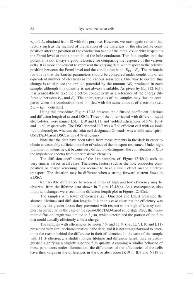
82 Dye-sensitized solar cells
tn and Ln obtained from IS with this purpose. However, we must again remark that factors such as the method of preparation of the materials or the electrolyte com-position alter the position of the conduction band of the metal oxide with respect to the Fermi level or redox potential of the hole conductor. This fact implies that the potential is not always a good reference for comparing the response of the various cells. It is more convenient to represent the varying data with respect to the relative position between the Fermi level and the conduction band, EFn − EC. The rationale for this is that the kinetic parameters should be compared under conditions of an equivalent number of electrons in the various solar cells. One way to correct this change is to displace the applied potential by the amount ΔEC produced in each sample, although this quantity is not always available. As given by Eq. (12.165), it is reasonable to take the electron conductivity as a reference of the energy dif-ference between EFn and EC. The characteristics of the samples may thus be com-pared when the conduction band is fi lled with the same amount of electrons (i.e., EFn − EC = constant).
Using this procedure, Figure 12.48 presents the diffusion coeffi cient, lifetime and diffusion length of several DSCs. Three of them, fabricated with different liquid electrolytes, were named L5Li, L10 and L11, and yielded effi ciencies of 5 %, 10 % and 11 %, respectively. The DSC denoted IL7 was a 7 % effi cient cell with an ionic liquid electrolyte, whereas the solar cell designated Ometad4 was a solid state spiro-OMeTAD-based DSC, with a 4 % effi ciency.
Note that the data have been taken from measurements in the dark in order to obtain a reasonably suffi cient number of values of the transport resistance. Under high illumination intensities, it became very diffi cult to distinguish the contribution of Rt to the impedance spectra from other resistive elements.
The diffusion coeffi cients of the fi ve samples, cf. Figure 12.48(a), took on very similar values in all cases. Therefore, factors such as the hole conductor com-position or charge screening ions seemed to have a small effect on the electron transport. The situation may be different when a strong forward current fl ows in a DSC.
Remarkable differences between samples of high and low effi ciency may be observed from the lifetime data shown in Figure 12.48(b). As a consequence, also important changes were seen in the diffusion length plot in Figure 12.48(c).
The samples with lower effi ciencies (i.e., Ometad4 and L5Li) presented the shortest lifetimes and diffusion lengths. It is in this case clear that the effi ciency was limited by the greater losses they presented with respect to the high-effi ciency sam-ples. In particular, in the case of the spiro-OMeTAD-based solid state DSC, the maxi-mum diffusion length was limited to 3 mm, which determined the portion of the fi lm that could actually effi ciently collect charge.
The samples with effi ciencies between 7 % and 11 % (i.e., IL7, L10 and L11) presented very similar characteristics in the dark, and it is not straightforward to deter-mine the reason behind the difference in their effi ciencies. In the case of the sample with 11 % effi ciency, a slightly longer lifetime and diffusion length may be distin-guished signifying a slightly superior fi lm quality. Assuming a similar behavior of these parameters under illumination, the differences of the effi ciencies of the cells have their origin in the differences in the dye absorption (K19 in IL7 and N719 in
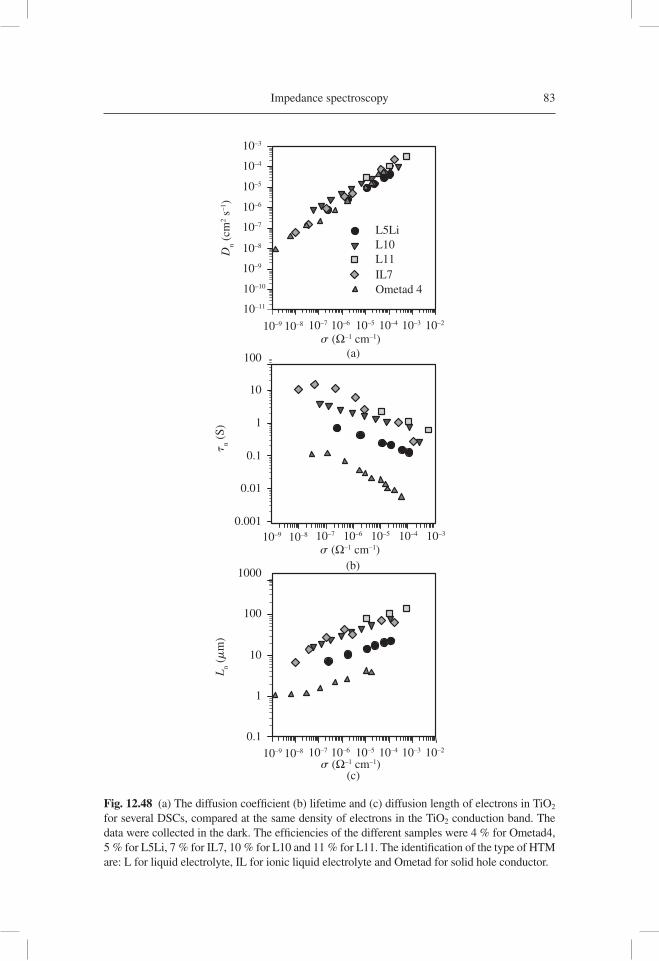
Impedance spectroscopy 83
10–3
10–4
L5LiL10L11IL7Ometad 4
10–5
10–6
10–7
10–7 10–6
s (Ω–1 cm–1)(a)
(b)
(c)
10–5 10–4 10–3 10–2
10–8
10–8
10–9
Dn (
cm2 s
–1)
10–10
10–11
100
10
1
0.1
0.01
tn (
S)
0.001
1000
100
10
Ln (m
m)
1
0.1
10–9
10–7 10–6
s (Ω–1 cm–1)10–5 10–4 10–310–810–9
10–7 10–6
s (Ω–1 cm–1)10–5 10–4 10–3 10–210–810–9
Fig. 12.48 (a) The diffusion coeffi cient (b) lifetime and (c) diffusion length of electrons in TiO2 for several DSCs, compared at the same density of electrons in the TiO2 conduction band. The data were collected in the dark. The effi ciencies of the different samples were 4 % for Ometad4, 5 % for L5Li, 7 % for IL7, 10 % for L10 and 11 % for L11. The identifi cation of the type of HTM are: L for liquid electrolyte, IL for ionic liquid electrolyte and Ometad for solid hole conductor.
84 Dye-sensitized solar cells
10–7 10–6 10–5
s (Ω–1 cm–1)
r r (Ω
cm
3 )
10–4 10–3 10–210–810–9
0.001
0.01
0.1
1
10
100
1000
L5Li
L10
L11
IL7
Ometad 4
Fig. 12.49 Charge transfer resistances of various DSCs in the dark, compared at the same elec-tron density in the conduction band.
L10 and L11), and electron injection into the TiO2, which provides higher values of current and potential [12.68].
While it is customary to analyze the performance of DSC in terms of the time constants mentioned before, and this is convenient in certain respects (especially if the diffusion length is short), it should be emphasized that the differences in the char-acteristics of the DSCs shown in Figure 12.48 have their origin in the values of the recombination resistance, as can be seen in Figure 12.49. In order to compare the dif-ferent cells, it is important to utilize the volumetric recombination resistance. Thus, the recombination resistance rises from the Ometad4 sample to L5Li and then to the rest of the samples. Consistent with the highest energy conversion effi ciency, L11 is the one that has the higher rr.
Therefore, concerning the DSC performance in general, it should be concluded that once the dye provides the charge injection level in the cell (and assuming that dye regeneration is fast), the charge transfer from TiO2 to the hole conductor is the main process determining the potential of a particular cell to perform at a certain effi ciency. This aspect will be treated in more detail in the last section.
Particularly, in the case of the spiro-OMeTAD solid state solar cell, any enhance-ment of the cell has to involve an increase in Rrec or the use of materials with higher conductivity rendering it possible to increase the diffusion length of carriers in the metal-oxide semiconductor.
12.7.3 Nanotubes
It is believed that an improvement in the structural order of the electron-conduct-ing metal oxide networks may enhance their electronic transport characteristics, and provide improved DSC effi ciencies. A number of structures have been prepared and
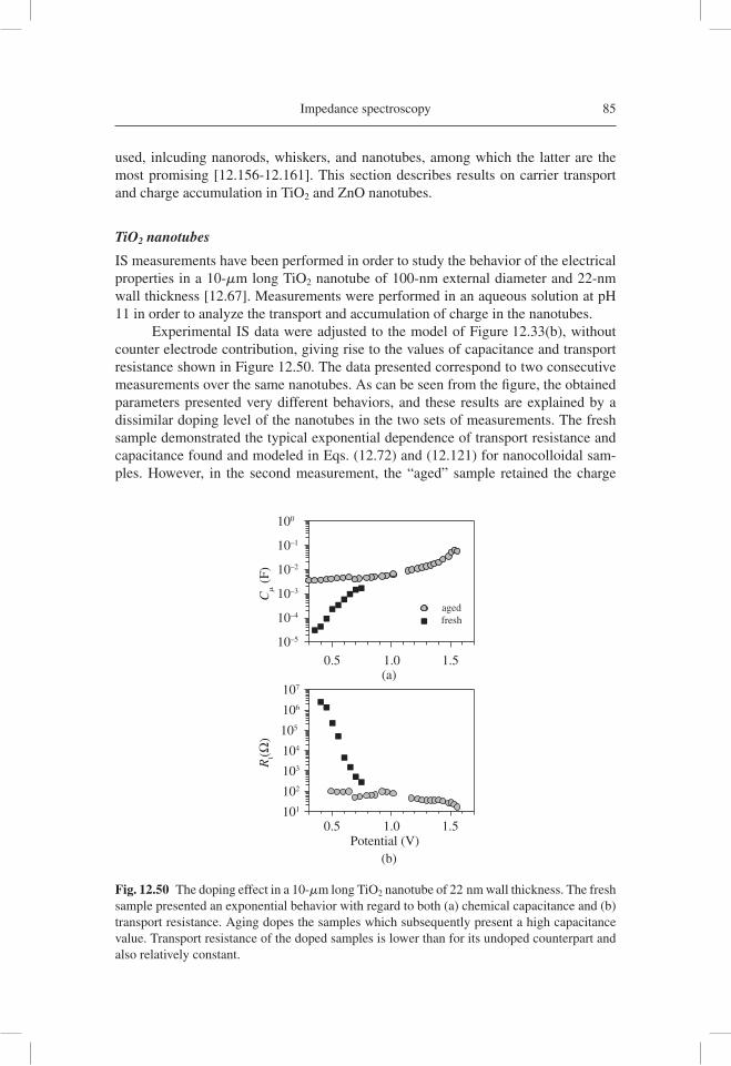
Impedance spectroscopy 85
used, inlcuding nanorods, whiskers, and nanotubes, among which the latter are the most promising [12.156-12.161]. This section describes results on carrier transport and charge accumulation in TiO2 and ZnO nanotubes.
TiO2 nanotubes
IS measurements have been performed in order to study the behavior of the electrical properties in a 10-mm long TiO2 nanotube of 100-nm external diameter and 22-nm wall thickness [12.67]. Measurements were performed in an aqueous solution at pH 11 in order to analyze the transport and accumulation of charge in the nanotubes.
Experimental IS data were adjusted to the model of Figure 12.33(b), without counter electrode contribution, giving rise to the values of capacitance and transport resistance shown in Figure 12.50. The data presented correspond to two consecutive measurements over the same nanotubes. As can be seen from the fi gure, the obtained parameters presented very different behaviors, and these results are explained by a dissimilar doping level of the nanotubes in the two sets of measurements. The fresh sample demonstrated the typical exponential dependence of transport resistance and capacitance found and modeled in Eqs. (12.72) and (12.121) for nanocolloidal sam-ples. However, in the second measurement, the “aged” sample retained the charge
101
102
103
104
105
106
107
Potential (V)
Rt(Ω
)
0.5 1.0 1.5
Cm (
F)
0.510–5
10–4
10–3
10–2
10–1
100
1.0(a)
(b)
1.5
agedfresh
Fig. 12.50 The doping effect in a 10-mm long TiO2 nanotube of 22 nm wall thickness. The fresh sample presented an exponential behavior with regard to both (a) chemical capacitance and (b) transport resistance. Aging dopes the samples which subsequently present a high capacitance value. Transport resistance of the doped samples is lower than for its undoped counterpart and also relatively constant.
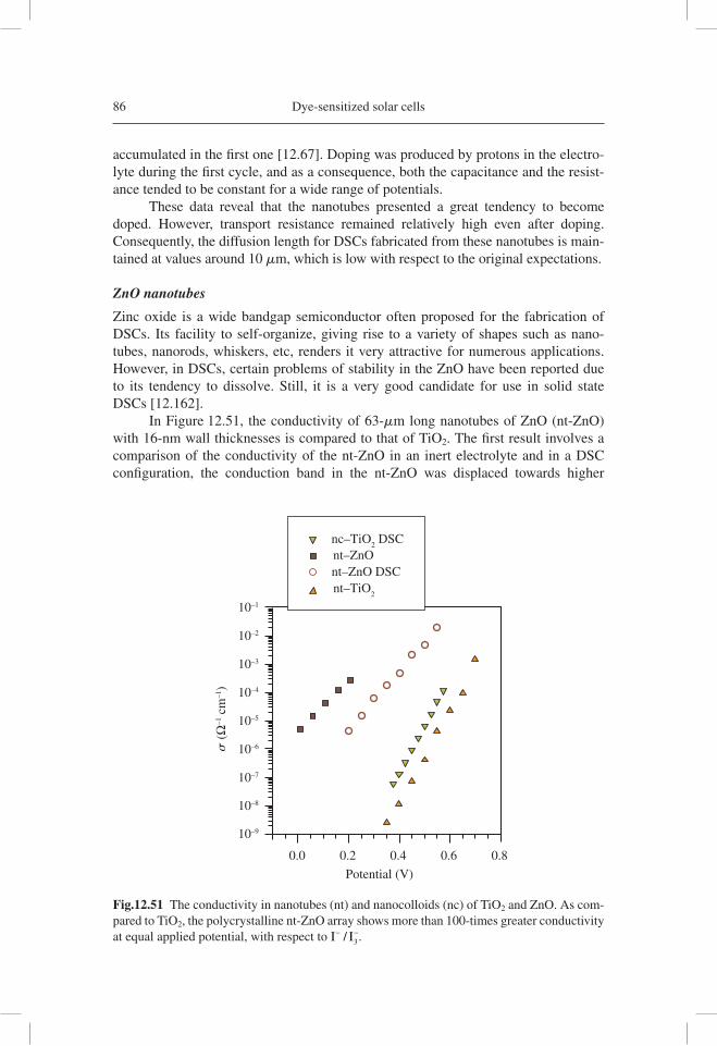
86 Dye-sensitized solar cells
accumulated in the fi rst one [12.67]. Doping was produced by protons in the electro-lyte during the fi rst cycle, and as a consequence, both the capacitance and the resist-ance tended to be constant for a wide range of potentials.
These data reveal that the nanotubes presented a great tendency to become doped. However, transport resistance remained relatively high even after doping. Consequently, the diffusion length for DSCs fabricated from these nanotubes is main-tained at values around 10 mm, which is low with respect to the original expectations.
ZnO nanotubes
Zinc oxide is a wide bandgap semiconductor often proposed for the fabrication of DSCs. Its facility to self-organize, giving rise to a variety of shapes such as nano-tubes, nanorods, whiskers, etc, renders it very attractive for numerous applications. However, in DSCs, certain problems of stability in the ZnO have been reported due to its tendency to dissolve. Still, it is a very good candidate for use in solid state DSCs [12.162].
In Figure 12.51, the conductivity of 63-mm long nanotubes of ZnO (nt-ZnO) with 16-nm wall thicknesses is compared to that of TiO2. The fi rst result involves a comparison of the conductivity of the nt-ZnO in an inert electrolyte and in a DSC confi guration, the conduction band in the nt-ZnO was displaced towards higher
10–9
10–8
10–7
10–6
10–5
10–4
10–3
10–2
10–1
Potential (V)
s (Ω
–1 c
m–1
)
0.20.0 0.4 0.6 0.8
nc–TiO2 DSC
nt–ZnOnt–ZnO DSCnt–TiO
2
Fig.12.51 The conductivity in nanotubes (nt) and nanocolloids (nc) of TiO2 and ZnO. As com-pared to TiO2, the polycrystalline nt-ZnO array shows more than 100-times greater conductivity at equal applied potential, with respect to I I− −/ 3.
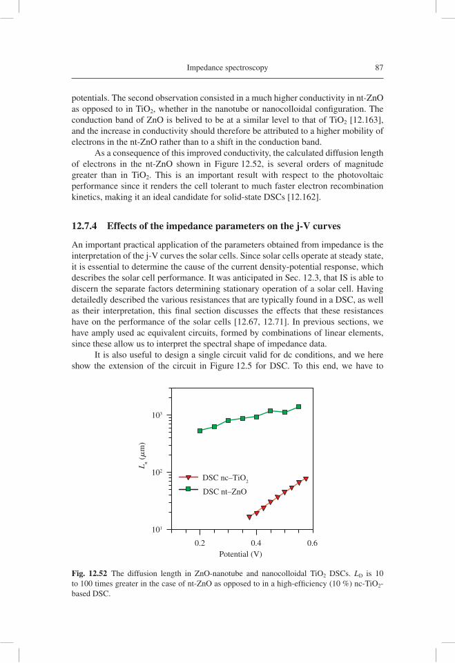
Impedance spectroscopy 87
Potential (V)
Ln (m
m)
101
102
103
0.2 0.4 0.6
DSC nc–TiO2
DSC nt–ZnO
Fig. 12.52 The diffusion length in ZnO-nanotube and nanocolloidal TiO2 DSCs. LD is 10 to 100 times greater in the case of nt-ZnO as opposed to in a high-effi ciency (10 %) nc-TiO2-based DSC.
potentials. The second observation consisted in a much higher conductivity in nt-ZnO as opposed to in TiO2, whether in the nanotube or nanocolloidal confi guration. The conduction band of ZnO is belived to be at a similar level to that of TiO2 [12.163], and the increase in conductivity should therefore be attributed to a higher mobility of electrons in the nt-ZnO rather than to a shift in the conduction band.
As a consequence of this improved conductivity, the calculated diffusion length of electrons in the nt-ZnO shown in Figure 12.52, is several orders of magnitude greater than in TiO2. This is an important result with respect to the photovoltaic performance since it renders the cell tolerant to much faster electron recombination kinetics, making it an ideal candidate for solid-state DSCs [12.162].
12.7.4 Effects of the impedance parameters on the j-V curves
An important practical application of the parameters obtained from impedance is the interpretation of the j-V curves the solar cells. Since solar cells operate at steady state, it is essential to determine the cause of the current density-potential response, which describes the solar cell performance. It was anticipated in Sec. 12.3, that IS is able to discern the separate factors determining stationary operation of a solar cell. Having detailedly described the various resistances that are typically found in a DSC, as well as their interpretation, this fi nal section discusses the effects that these resistances have on the performance of the solar cells [12.67, 12.71]. In previous sections, we have amply used ac equivalent circuits, formed by combinations of linear elements, since these allow us to interpret the spectral shape of impedance data.
It is also useful to design a single circuit valid for dc conditions, and we here show the extension of the circuit in Figure 12.5 for DSC. To this end, we have to
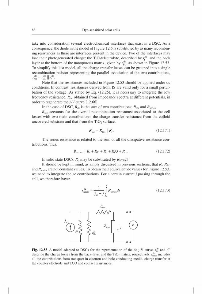
88 Dye-sensitized solar cells
take into consideration several electrochemical interfaces that exist in a DSC. As a consequence, the diode in the model of Figure 12.5 is substituted by as many recombin-ing resistances as there are interfaces present in the device. Two of the interfaces may lose their photogenerated charge: the TiO2/electrolyte, described by rr
dc, and the back layer at the bottom of the nanoporous matrix, given by rBL
dc, as shown in Figure 12.53. To simplify this last model, all the charge transfer losses can be grouped into a single recombination resistor representing the parallel association of the two contributions, r r rrec
dcBLdc
rdc= || .
Note that the resistances included in Figure 12.53 should be applied under dc conditions. In contrast, resistances derived from IS are valid only for a small pertur-bation of the voltage. As stated by Eq. (12.25), it is necessary to integrate the low frequency resistance, Rdc, obtained from impedance spectra at different potentials, in order to regenerate the j-V curve [12.66].
In the case of DSC, Rdc is the sum of two contributions: Rrec and Rseries.Rrec accounts for the overall recombination resistance associated to the cell
losses with two main contributions: the charge transfer resistance from the colloid uncovered substrate and that from the TiO2 surface.
R R Rrec BL r= || . (12.171)
The series resistance is related to the sum of all the dissipative resistance con-tributions, thus:
Rseries = Rs + RPt + Rd + Rt/3 + Rco. (12.172)
In solid state DSCs, Rd may be substituted by RHTM/3.It should be kept in mind, as amply discussed in previous sections, that Rr, RBL
and Rseries are not constant values. To obtain their equivalent dc values for Figure 12.53, we need to integrate the ac contributions. For a certain current j passing through the cell, we therefore have:
rj j
R dij
j
seriesdc
scseries
sc
=− ∫1
(12.173)
Zload
dcBLr
dcseriesr
dcrr
jsc
j V
Fig. 12.53 A model adapted to DSCs for the representation of the dc j-V curve. rBLdc and rr
dc describe the charge losses from the back-layer and the TiO2 matrix, respectively. rseries
dc includes all the contributions from transport in electron and hole conducting media, charge transfer at the counter electrode and TCO and contact resistances.
Impedance spectroscopy 89
rj j
R dij
j
recdc
screc
sc
=− ∫1
(12.174)
Alternatively, to determine the dc contribution of the resistances at a certain applied potential, we can write:
rV
dV
R
V
seriesdc
series
= ∫1
0
(12.175)
rV
dV
R
V
recdc
rec
= ∫1
0
(12.176)
It is convenient to discuss here the existence of a shunt resistance in DSCs. In crystalline silicon solar cells, rshunt is a constant resistance accounting for leakage cur-rents crossing the cell [12.71]. Recent studies have revealed that rshunt may change with the measuring conditions, though these variations are not fully understood [12.95]. In DSC the closest element to rshunt is rBL, however it has to be taken into consideration that rBL is a variable resistor that depends on the potential. It can be obtained from:
rV
dV
R
V
BLdc
BL
= ∫1
0
(12.177)
with RBL following a Tafel response as the current losses occur at the back layer/ electrolyte interface. In order to apply the dc models used in crystalline silicon solar cells in DSCs, we thus have to substitute rshunt in Figure 12.5 by another diode governed by an ideality factor given by the transfer coeffi cient characteristic of the back layer. This is the two-diode model approach used in other types of solar cells [12.164, 12.165].
Once the contributions of the various parameters are identifi ed, it is possible to clarify how they infl uence the j-V curves.
Effect of series resistance
Figure 12.54 presents the effect of the series resistance on the j-V curve. The rise in rseries
dc reduces the FF and, consequently, the effi ciency of the solar cell. If rseriesdc is too
large, also jsc becomes affected. The same effect occurs with large photogenerated currents: the higher the current crossing the cell, the greater is the drop in potential due to the series resistance corrections, and thus also drops in the FF and effi ciency.
The series resistance is a very important limiting factor in solar cells, specially if the objective is to scale them up to large area cells or to use dyes with enhanced injection properties. In such cases, a correct choice of the geometric design and the materials employed for collecting the charge and regenerating the dyes is crucial in order to minimize this resistance.
From another point of view, once the cell is fabricated, we may use the integrated series resistance to evaluate the improvements that could be obtained by partially or completely eliminating rseries
dc . To do so, we simply need to subtract the ohmic drop at the series resistance from the applied potential to obtain the corrected potential:
V V i r V R dii
c seriesdc
series= − = − ∫0
(12.178)
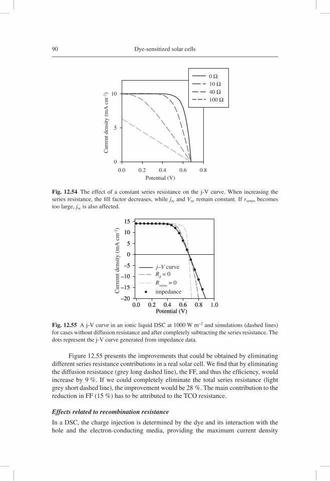
90 Dye-sensitized solar cells
Figure 12.55 presents the improvements that could be obtained by eliminating different series resistance contributions in a real solar cell. We fi nd that by eliminating the diffusion resistance (grey long dashed line), the FF, and thus the effi ciency, would increase by 9 %. If we could completely eliminate the total series resistance (light grey short dashed line), the improvement would be 28 %. The main contribution to the reduction in FF (15 %) has to be attributed to the TCO resistance.
Effects related to recombination resistance
In a DSC, the charge injection is determined by the dye and its interaction with the hole and the electron-conducting media, providing the maximum current density
Potential (V)
Cur
rem
t den
sity
(m
A c
m–2
)
–20
–15
–10
–5
0
5
10
15
0.20.0 0.4 0.6 0.8 1.0Potential (V)
–20
–15
–10
–5
0
5
10
15
0.20.0 0.4 0.6 0.8 1.0
j–V curveR
d = 0
Rseries
= 0
impedance
Fig. 12.55 A j-V curve in an ionic liquid DSC at 1000 W m−2 and simulations (dashed lines) for cases without diffusion resistance and after completely subtracting the series resistance. The dots represent the j-V curve generated from impedance data.
Potential (V)0.2 0.4 0.6 0.80.0
0
Cur
rent
den
sity
(m
A c
m–2
)
5
10
0 Ω10 Ω40 Ω100 Ω
Fig. 12.54 The effect of a constant series resistance on the j-V curve. When increasing the series resistance, the fi ll factor decreases, while jsc and Voc remain constant. If rseries becomes too large, jsc is also affected.
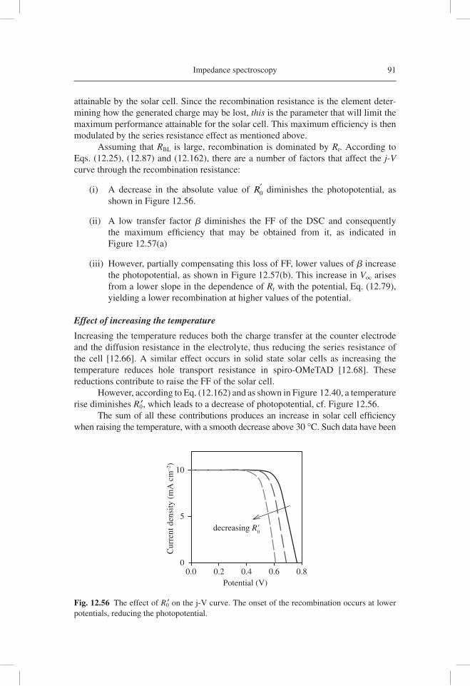
Impedance spectroscopy 91
attainable by the solar cell. Since the recombination resistance is the element deter-mining how the generated charge may be lost, this is the parameter that will limit the maximum performance attainable for the solar cell. This maximum effi ciency is then modulated by the series resistance effect as mentioned above.
Assuming that RBL is large, recombination is dominated by Rr. According to Eqs. (12.25), (12.87) and (12.162), there are a number of factors that affect the j-V curve through the recombination resistance:
(i) A decrease in the absolute value of R0′ diminishes the photopotential, as
shown in Figure 12.56.
(ii) A low transfer factor b diminishes the FF of the DSC and consequently the maximum effi ciency that may be obtained from it, as indicated in Figure 12.57(a)
(iii) However, partially compensating this loss of FF, lower values of b increase the photopotential, as shown in Figure 12.57(b). This increase in Voc arises from a lower slope in the dependence of Rr with the potential, Eq. (12.79), yielding a lower recombination at higher values of the potential.
Effect of increasing the temperature
Increasing the temperature reduces both the charge transfer at the counter electrode and the diffusion resistance in the electrolyte, thus reducing the series resistance of the cell [12.66]. A similar effect occurs in solid state solar cells as increasing the temperature reduces hole transport resistance in spiro-OMeTAD [12.68]. These reductions contribute to raise the FF of the solar cell.
However, according to Eq. (12.162) and as shown in Figure 12.40, a temperature rise diminishes R0′, which leads to a decrease of photopotential, cf. Figure 12.56.
The sum of all these contributions produces an increase in solar cell effi ciency when raising the temperature, with a smooth decrease above 30 °C. Such data have been
0.2 0.4 0.6 0.80.00
5
10
decreasing R'0
Potential (V)
Cur
rent
den
sity
(m
A c
m–2
)
Fig. 12.56 The effect of R0′ on the j-V curve. The onset of the recombination occurs at lower potentials, reducing the photopotential.
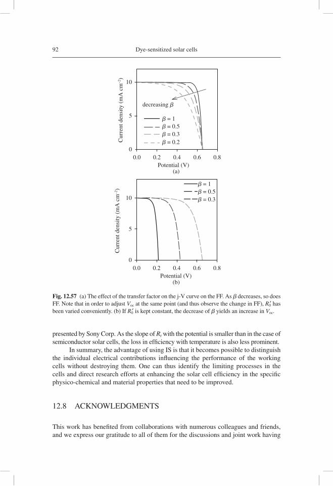
92 Dye-sensitized solar cells
presented by Sony Corp. As the slope of Rr with the potential is smaller than in the case of semiconductor solar cells, the loss in effi ciency with temperature is also less prominent.
In summary, the advantage of using IS is that it becomes possible to distinguish the individual electrical contributions infl uencing the performance of the working cells without destroying them. One can thus identify the limiting processes in the cells and direct research efforts at enhancing the solar cell effi ciency in the specifi c physico-chemical and material properties that need to be improved.
12.8 ACKNOWLEDGMENTS
This work has benefi ted from collaborations with numerous colleagues and friends, and we express our gratitude to all of them for the discussions and joint work having
0.00
5
10
Potential (V)0.0
0
5
10
0.2
decreasing b
0.4
(a)
(b)
0.6 0.8
0.2Potential (V)
Cur
rent
den
sity
(m
A c
m–2
)C
urre
nt d
ensi
ty (
mA
cm
–2)
0.4 0.6 0.8
b = 1b = 0.5b = 0.3
b = 1b = 0.5b = 0.3b = 0.2
Fig. 12.57 (a) The effect of the transfer factor on the j-V curve on the FF. As b decreases, so does FF. Note that in order to adjust Voc at the same point (and thus observe the change in FF), R0′ has been varied conveniently. (b) If R0′ is kept constant, the decrease of b yields an increase in Voc.
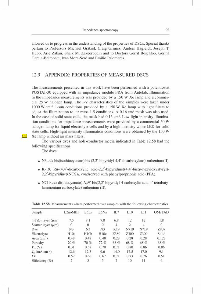
Impedance spectroscopy 93
allowed us to progress in the understanding of the properties of DSCs. Special thanks pertain to Professors Michael Grätzel, Craig Grimes, Anders Hagfeldt, Joseph T. Hupp, Arie Zaban, Shaik M. Zakeeruddin and to Doctors Gerrit Boschloo, Germà Garcia-Belmonte, Ivan Mora-Seró and Emilio Palomares.
12.9 APPENDIX: PROPERTIES OF MEASURED DSCS
The measurements presented in this work have been performed with a potentiostat PGSTAT-30 equipped with an impedance module FRA from Autolab. Illumination in the impedance measurements was provided by a 150 W Xe lamp and a commer-cial 25 W halogen lamp. The j-V characteristics of the samples were taken under 1000 W cm−2 1-sun conditions provided by a 150 W Xe lamp with light fi lters to adjust the illumination to air mass 1.5 conditions. A 0.16 cm2 mask was also used. In the case of solid state cells, the mask had 0.13 cm2. Low light intensity illumina-tion conditions for impedance measurements were provided by a commercial 50 W halogen lamp for liquid electrolyte cells and by a high intensity white LED for solid state cells. High-light intensity illumination conditions were obtained by the 150 W Xe lamp without air mass fi lters.
The various dyes and hole-conductor media indicated in Table 12.58 had the following specifi cations:
The dyes:
● N3, cis-bis(isothiocyanato) bis (2,2′-bipyridyl-4,4′-dicarboxylato)-ruthenium(II).
● K-19, Ru-(4,4′-dicarboxylic acid-2,2′-bipyridine)(4,4′-bis(p-hexyloxystyryl)- 2,2′-bipyridine)(NCS)2, coadsorved with phenylproprionic acid (PPA).
● N719, cis-di(thiocyanato)-N,N′-bis(2,2′-bipyridyl-4-carboxylic acid-4′-tetrabuty-lammonium carboxylate) ruthenium (II).
Q2
Table 12.58 Measurements where performed over samples with the following characteristics.
Sample L2noMBI L5Li L5Na IL7 L10 L11 OMeTAD
n-TiO2 layer (mm) 7.5 8.1 7.0 6.8 12 12 1.8Scatter layer (mm) 0 0 0 4 2 4 0Dye N3 N3 N3 K19 N719 N719 Z907Electrolyte H10a H10b H10c Z380 Z300 Z300 SolidArea (cm2) 0.48 0.48 0.48 0.28 0.28 0.28 0.128Porosity 70 % 70 % 72 % 68 % 68 % 68 % 68 %Voc (V) 0.31 0.58 0.70 0.71 0.80 0.86 0.86Jsc (mA cm−2) 12.6 12.3 9.6 14.0 17.5 17.0 9.1FF 0.52 0.66 0.67 0.71 0.73 0.76 0.51Effi ciency (%) 2 5 5 7 10 11 4
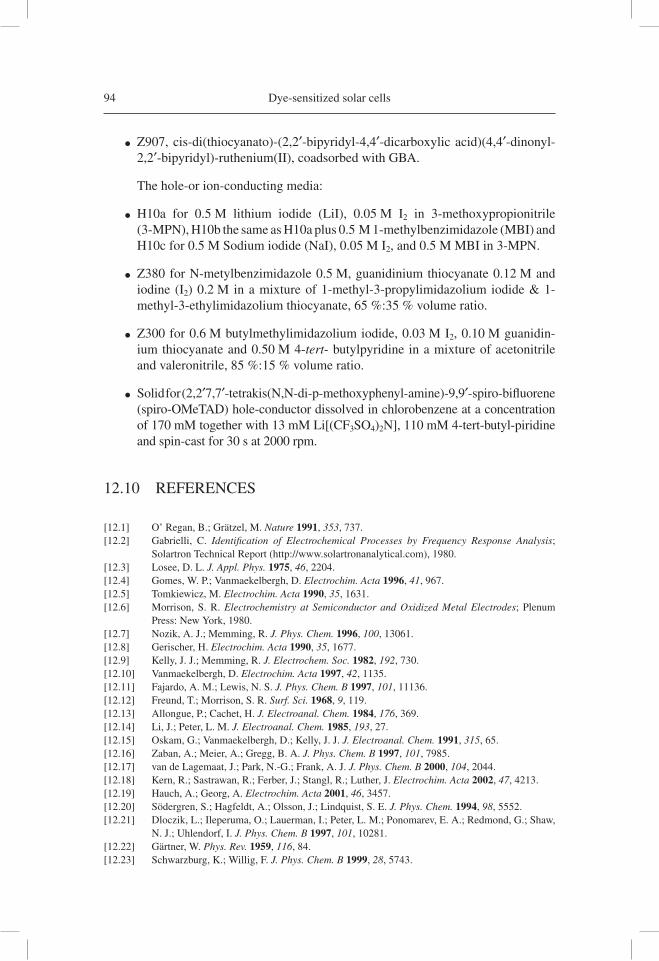
94 Dye-sensitized solar cells
● Z907, cis-di(thiocyanato)-(2,2′-bipyridyl-4,4′-dicarboxylic acid)(4,4′-dinonyl-2,2′-bipyridyl)-ruthenium(II), coadsorbed with GBA.
The hole-or ion-conducting media:
● H10a for 0.5 M lithium iodide (LiI), 0.05 M I2 in 3-methoxypropionitrile (3-MPN), H10b the same as H10a plus 0.5 M 1-methylbenzimidazole (MBI) and H10c for 0.5 M Sodium iodide (NaI), 0.05 M I2, and 0.5 M MBI in 3-MPN.
● Z380 for N-metylbenzimidazole 0.5 M, guanidinium thiocyanate 0.12 M and iodine (I2) 0.2 M in a mixture of 1-methyl-3-propylimidazolium iodide & 1-methyl-3-ethylimidazolium thiocyanate, 65 %:35 % volume ratio.
● Z300 for 0.6 M butylmethylimidazolium iodide, 0.03 M I2, 0.10 M guanidin-ium thiocyanate and 0.50 M 4-tert- butylpyridine in a mixture of acetonitrile and valeronitrile, 85 %:15 % volume ratio.
● Solid for (2,2′7,7′-tetrakis(N,N-di-p-methoxyphenyl-amine)-9,9′-spiro- bifl uorene (spiro-OMeTAD) hole-conductor dissolved in chlorobenzene at a concentration of 170 mM together with 13 mM Li[(CF3SO4)2N], 110 mM 4-tert-butyl-piridine and spin-cast for 30 s at 2000 rpm.
12.10 REFERENCES
[12.1] O’ Regan, B.; Grätzel, M. Nature 1991, 353, 737.[12.2] Gabrielli, C. Identifi cation of Electrochemical Processes by Frequency Response Analysis;
Solartron Technical Report (http://www.solartronanalytical.com), 1980.[12.3] Losee, D. L. J. Appl. Phys. 1975, 46, 2204.[12.4] Gomes, W. P.; Vanmaekelbergh, D. Electrochim. Acta 1996, 41, 967.[12.5] Tomkiewicz, M. Electrochim. Acta 1990, 35, 1631.[12.6] Morrison, S. R. Electrochemistry at Semiconductor and Oxidized Metal Electrodes; Plenum
Press: New York, 1980.[12.7] Nozik, A. J.; Memming, R. J. Phys. Chem. 1996, 100, 13061.[12.8] Gerischer, H. Electrochim. Acta 1990, 35, 1677.[12.9] Kelly, J. J.; Memming, R. J. Electrochem. Soc. 1982, 192, 730.[12.10] Vanmaekelbergh, D. Electrochim. Acta 1997, 42, 1135.[12.11] Fajardo, A. M.; Lewis, N. S. J. Phys. Chem. B 1997, 101, 11136.[12.12] Freund, T.; Morrison, S. R. Surf. Sci. 1968, 9, 119.[12.13] Allongue, P.; Cachet, H. J. Electroanal. Chem. 1984, 176, 369.[12.14] Li, J.; Peter, L. M. J. Electroanal. Chem. 1985, 193, 27.[12.15] Oskam, G.; Vanmaekelbergh, D.; Kelly, J. J. J. Electroanal. Chem. 1991, 315, 65.[12.16] Zaban, A.; Meier, A.; Gregg, B. A. J. Phys. Chem. B 1997, 101, 7985.[12.17] van de Lagemaat, J.; Park, N.-G.; Frank, A. J. J. Phys. Chem. B 2000, 104, 2044.[12.18] Kern, R.; Sastrawan, R.; Ferber, J.; Stangl, R.; Luther, J. Electrochim. Acta 2002, 47, 4213.[12.19] Hauch, A.; Georg, A. Electrochim. Acta 2001, 46, 3457.[12.20] Södergren, S.; Hagfeldt, A.; Olsson, J.; Lindquist, S. E. J. Phys. Chem. 1994, 98, 5552.[12.21] Dloczik, L.; Ileperuma, O.; Lauerman, I.; Peter, L. M.; Ponomarev, E. A.; Redmond, G.; Shaw,
N. J.; Uhlendorf, I. J. Phys. Chem. B 1997, 101, 10281.[12.22] Gärtner, W. Phys. Rev. 1959, 116, 84.[12.23] Schwarzburg, K.; Willig, F. J. Phys. Chem. B 1999, 28, 5743.
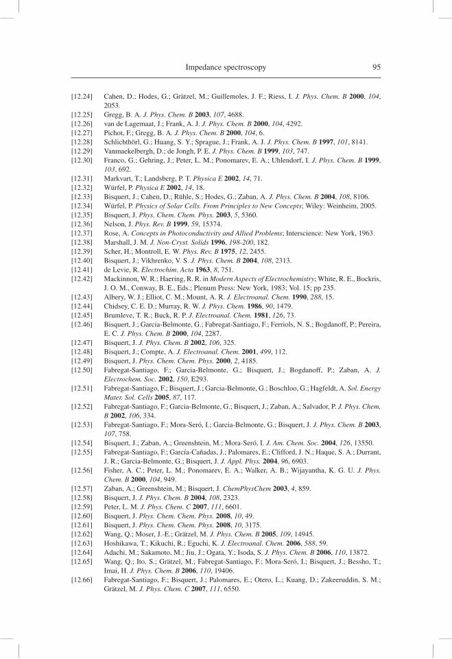
Impedance spectroscopy 95
[12.24] Cahen, D.; Hodes, G.; Grätzel, M.; Guillemoles, J. F.; Riess, I. J. Phys. Chem. B 2000, 104, 2053.
[12.25] Gregg, B. A. J. Phys. Chem. B 2003, 107, 4688.[12.26] van de Lagemaat, J.; Frank, A. J. J. Phys. Chem. B 2000, 104, 4292.[12.27] Pichot, F.; Gregg, B. A. J. Phys. Chem. B 2000, 104, 6.[12.28] Schlichthörl, G.; Huang, S. Y.; Sprague, J.; Frank, A. J. J. Phys. Chem. B 1997, 101, 8141.[12.29] Vanmaekelbergh, D.; de Jongh, P. E. J. Phys. Chem. B 1999, 103, 747.[12.30] Franco, G.; Gehring, J.; Peter, L. M.; Ponomarev, E. A.; Uhlendorf, I. J. Phys. Chem. B 1999,
103, 692.[12.31] Markvart, T.; Landsberg, P. T. Physica E 2002, 14, 71.[12.32] Würfel, P. Physica E 2002, 14, 18.[12.33] Bisquert, J.; Cahen, D.; Rühle, S.; Hodes, G.; Zaban, A. J. Phys. Chem. B 2004, 108, 8106.[12.34] Würfel, P. Physics of Solar Cells. From Principles to New Concepts; Wiley: Weinheim, 2005.[12.35] Bisquert, J. Phys. Chem. Chem. Phys. 2003, 5, 5360.[12.36] Nelson, J. Phys. Rev. B 1999, 59, 15374.[12.37] Rose, A. Concepts in Photoconductivity and Allied Problems; Interscience: New York, 1963.[12.38] Marshall, J. M. J. Non-Cryst. Solids 1996, 198-200, 182.[12.39] Scher, H.; Montroll, E. W. Phys. Rev. B 1975, 12, 2455.[12.40] Bisquert, J.; Vikhrenko, V. S. J. Phys. Chem. B 2004, 108, 2313.[12.41] de Levie, R. Electrochim. Acta 1963, 8, 751.[12.42] Mackinnon, W. R.; Haering, R. R. in Modern Aspects of Electrochemistry; White, R. E., Bockris,
J. O. M., Conway, B. E., Eds.; Plenum Press: New York, 1983; Vol. 15; pp 235.[12.43] Albery, W. J.; Elliot, C. M.; Mount, A. R. J. Electroanal. Chem. 1990, 288, 15.[12.44] Chidsey, C. E. D.; Murray, R. W. J. Phys. Chem. 1986, 90, 1479.[12.45] Brumleve, T. R.; Buck, R. P. J. Electroanal. Chem. 1981, 126, 73.[12.46] Bisquert, J.; Garcia-Belmonte, G.; Fabregat-Santiago, F.; Ferriols, N. S.; Bogdanoff, P.; Pereira,
E. C. J. Phys. Chem. B 2000, 104, 2287.[12.47] Bisquert, J. J. Phys. Chem. B 2002, 106, 325.[12.48] Bisquert, J.; Compte, A. J. Electroanal. Chem. 2001, 499, 112.[12.49] Bisquert, J. Phys. Chem. Chem. Phys. 2000, 2, 4185.[12.50] Fabregat-Santiago, F.; Garcia-Belmonte, G.; Bisquert, J.; Bogdanoff, P.; Zaban, A. J.
Electrochem. Soc. 2002, 150, E293.[12.51] Fabregat-Santiago, F.; Bisquert, J.; Garcia-Belmonte, G.; Boschloo, G.; Hagfeldt, A. Sol. Energy
Mater. Sol. Cells 2005, 87, 117.[12.52] Fabregat-Santiago, F.; Garcia-Belmonte, G.; Bisquert, J.; Zaban, A.; Salvador, P. J. Phys. Chem.
B 2002, 106, 334.[12.53] Fabregat-Santiago, F.; Mora-Seró, I.; Garcia-Belmonte, G.; Bisquert, J. J. Phys. Chem. B 2003,
107, 758.[12.54] Bisquert, J.; Zaban, A.; Greenshtein, M.; Mora-Seró, I. J. Am. Chem. Soc. 2004, 126, 13550.[12.55] Fabregat-Santiago, F.; García-Cañadas, J.; Palomares, E.; Clifford, J. N.; Haque, S. A.; Durrant,
J. R.; Garcia-Belmonte, G.; Bisquert, J. J. Appl. Phys. 2004, 96, 6903.[12.56] Fisher, A. C.; Peter, L. M.; Ponomarev, E. A.; Walker, A. B.; Wijayantha, K. G. U. J. Phys.
Chem. B 2000, 104, 949.[12.57] Zaban, A.; Greenshtein, M.; Bisquert, J. ChemPhysChem 2003, 4, 859.[12.58] Bisquert, J. J. Phys. Chem. B 2004, 108, 2323.[12.59] Peter, L. M. J. Phys. Chem. C 2007, 111, 6601.[12.60] Bisquert, J. Phys. Chem. Chem. Phys. 2008, 10, 49.[12.61] Bisquert, J. Phys. Chem. Chem. Phys. 2008, 10, 3175.[12.62] Wang, Q.; Moser, J.-E.; Grätzel, M. J. Phys. Chem. B 2005, 109, 14945.[12.63] Hoshikawa, T.; Kikuchi, R.; Eguchi, K. J. Electroanal. Chem. 2006, 588, 59.[12.64] Adachi, M.; Sakamoto, M.; Jiu, J.; Ogata, Y.; Isoda, S. J. Phys. Chem. B 2006, 110, 13872.[12.65] Wang, Q.; Ito, S.; Grätzel, M.; Fabregat-Santiago, F.; Mora-Seró, I.; Bisquert, J.; Bessho, T.;
Imai, H. J. Phys. Chem. B 2006, 110, 19406.[12.66] Fabregat-Santiago, F.; Bisquert, J.; Palomares, E.; Otero, L.; Kuang, D.; Zakeeruddin, S. M.;
Grätzel, M. J. Phys. Chem. C 2007, 111, 6550.
96 Dye-sensitized solar cells
[12.67] Fabregat-Santiago, F.; Barea, E. M.; Bisquert, J.; Mor, G. K.; Shankar, K.; Grimes, C. A. J. Am. Chem. Soc. 2008, 130, 11312.
[12.68] Fabregat-Santiago, F.; Bisquert, J.; Cevey, L.; Chen, P.; Wang, M.; Zakeeruddin, S. M.; Grätzel, M. J. Am. Chem. Soc. 2009, 131, 558.
[12.69] Sah, C.-T. Fundamentals of Solid State Electronics; World Scientifi c: Singapur, 1991.[12.70] Prince, M. B. Journal of Applied Physics 1955, 26, 534.[12.71] Sze, S. M. Physics of Semiconductor Devizes, 2nd ed.; John Wiley and Sons: New York, 1981.[12.72] Jonscher, A. K. Dielectric Relaxation in Solids; Chelsea Dielectrics Press: London, 1983.[12.73] Macdonald, J. R. Impedance Spectroscopy; John Wiley and Sons: New York, 1987.[12.74] Bisquert, J. Electrochim. Acta 2002, 47, 2435.[12.75] Bisquert, J. Phys. Rev. B 2008, 77, 235203.[12.76] Mora-Seró, I.; Bisquert, J.; Fabregat-Santiago, F.; Garcia-Belmonte, G.; Zoppi, G.; Durose, K.;
Proskuryakov, Y. Y.; Oja, I.; Belaidi, A.; Dittrich, T.; Tena-Zaera, R.; Katty, A.; Lévy-Clement, C.; Barrioz, V.; Irvine, S. J. C. Nano Lett. 2006, 6, 640.
[12.77] Pajkossy, T. J. Electroanal. Chem. 1994, 364, 111.[12.78] Varney, R. N.; Fischer, L. H. Am. J. Phys. 1980, 48, 405.[12.79] Jamnik, J.; Maier, J. Phys. Chem. Chem. Phys. 2001, 3, 1668.[12.80] Glunz, S. W. Adv. Optoel. 2007, 97370.[12.81] Abayev, I.; Zaban, A.; Fabregat-Santiago, F.; Bisquert, J. Phys. Stat. Sol. (a) 2003, 196, R4.[12.82] Snaith, H. J.; Schmidt-Mende, L. Adv. Mat. 2007, 19, 3187.[12.83] Niinobe, D.; Makari, Y.; Kitamura, T.; Wada, Y.; Yanagida, S. J. Phys. Chem. B 2005, 109, 17892.[12.84] Zhang, Z.; Zakeeruddin, S. M.; O’Regan, B. C.; Humphry-Baker, R.; Grätzel, M. J. Phys. Chem.
B 2005, 109, 21818.[12.85] Berger, T.; Lana-Villarreal, T.; Monllor-Satoca, D.; Gomez, R. J. Phys. Chem. C 2007, 111,
9936.[12.86] Ruhle, S.; Greenshtein, M.; Chen, S.-G.; Merson, A.; Pizem, H.; Sukenik, C. S.; Cahen, D.;
Zaban, A. J. Phys. Chem. B 2005, 109, 18907.[12.87] Bisquert, J.; Fabregat-Santiago, F.; Mora-Seró, I.; Garcia-Belmonte, G.; Barea, E. M.; Palomares,
E. Inorg. Chim. Acta 2008, 361, 684.[12.88] Dor, S.; Ruhle, S.; Grinis, L.; Zaban, A. J. Phys. Chem. C 2009, 113, 2022.[12.89] Hamman, T. W.; Jensen, R. A.; Martinson, A. B. F.; Ryswykac, H. V.; Hupp, J. T. Energy
Environ. Sci. 2008, 1, 66.[12.90] Peter, L. M. J. Electroanal. Chem. 2007, 599, 233.[12.91] Mora-Seró, I.; Fabregat-Santiago, F.; Denier, B.; Bisquert, J.; Tena-Zaera, R.; Elias, J.; Lévy-
Clement, C. Appl. Phys. Lett. 2006, 89, 203117.[12.92] Mora-Seró, I.; Bisquert, J. Nano Lett. 2003, 3, 945.[12.93] Sato, N. Electrochemistry at Metal and Semiconductor Electrodes; Elsevier: Amsterdam,
1998.[12.94] Mora-Seró, I.; Garcia-Belmonte, G.; Boix, P. P.; Vázquez, M. A.; Bisquert, J. Energy Environ.
Sci. 2009, DOI:10.1039/B812468J.[12.95] Bashahu, M.; Nkundabakura, P. Solar Energy 2007, 81, 856.[12.96] Cameron, P. J.; Peter, L. M. J. Phys. Chem. B 2005, 109, 7392.[12.97] Huang, S. Y.; Schilchthörl, G.; Nozik, A. J.; Grätzel, M.; Frank, A. J. J. Phys. Chem. B 1997,
101, 2576.[12.98] Clifford, J. N.; Palomares, E.; Nazeeruddin, M. K.; Grätzel, M.; Durrant, J. R. J. Phys. Chem. C
2007, 111, 6561.[12.99] Lyon, L. A.; Hupp, J. T. J. Phys. Chem. B 1999, 103, 4623.[12.100] Miyashita, M.; Sunahara, K.; Nishikawa, T.; Uemura, Y.; Koumura, N.; Hara, K.; Mori, A.;
Abe, T.; Suzuki, E.; Mori, S. J. Am. Chem. Soc. 2008, 130, 17874.[12.101] Clifford, J. N.; Palomares, E.; Nazeeruddin, M. K.; Grätzel, M.; Nelson, J.; Li, X.; Long, N. J.;
Durrant, J. R. J. Am. Chem. Soc. 2004, 126, 5225.[12.102] Bisquert, J.; Zaban, A.; Salvador, P. J. Phys. Chem. B 2002, 106, 8774.[12.103] Salvador, P.; González-Hidalgo, M.; Zaban, A.; Bisquert, J. The Journal of Physical Chemistry
B 2005, 109, 15915.[12.104] Hens, Z. J. Phys. Chem. B 1999, 103, 122.
Impedance spectroscopy 97
[12.105] Hens, Z.; Gomes, W. P. J. Phys. Chem. B 1999, 103, 130.[12.106] Bisquert, J.; Zaban, A.; Greenshtein, M.; Mora-Sero, I. Journal of the American Chemical
Society 2004, 126, 13550.[12.107] Rickert, H. Electrochemistry of Solids; Springer Verlag: Berlin, 1982.[12.108] Bisquert, J.; Garcia-Belmonte, G.; Fabregat Santiago, F. J. Solid State Electrochem. 1999, 3,
337.[12.109] Turrión, M.; Bisquert, J.; Salvador, P. J. Phys. Chem. B 2003, 107, 9397.[12.110] Rühle, S.; Dittrich, T. J. Phys. Chem. B 2005, 109, 9522.[12.111] Lana-Villarreal, T.; Bisquert, J.; Mora-Seró, I.; Salvador, P. J. Phys. Chem. B 2005, 109,
10355.[12.112] Schiff, E. A. Sol. Energy Mater. Sol. Cells 2003, 78, 567.[12.113] Blom, P. W. M.; Vissenberg, M. C. J. M. Mat. Sci. Eng. R 2000, 27, 53.[12.114] Lampert, M. A.; Mark, P. Current Injection in Solids; Academic: New York, 1970.[12.115] Onsager, L.; Fuoss, R. M. J. Phys. Chem. 1932, 36, 2689.[12.116] Gomer, R. Rep. Prog. Phys. 1990, 53, 917.[12.117] Myshlyatsev, A. V.; Stepanov, A. A.; Uebing, C.; Zhdanov, V. P. Physical Review B 1995, 52,
5977.[12.118] Darken, L. S. Trans. Am. Inst. Min. Eng. 1948, 175, 184.[12.119] Tiedje, T.; Rose, A. Solid State Commun. 1981, 37, 49.[12.120] Orenstein, J.; Kastner, M. Phys. Rev. Lett. 1981, 46, 1421.[12.121] Hoesterey, D. C.; Letson, G. M. J. Phys. Chem. Solids 1963, 24, 1609.[12.122] Pomerantz, Z.; Zaban, A.; Ghosh, S.; Lellouche, J.-P.; Garcia-Belmonte, G.; Bisquert, J. J.
Electroanal. Chem. 2008, doi: 10.1016/j.jelechem.2007.11.005.[12.123] Bailes, M.; Cameron, P. J.; Lobato, K.; Peter, L. M. J. Phys. Chem. B 2005, 109, 15429.[12.124] van de Lagemaat, J.; Kopidakis, N.; Neale, N. R.; Frank, A. J. Phys. Rev. B 2005, 71, 035304.[12.125] Peter, L. M.; Dunn, H. K. J. Phys. Chem. C 2009, 113, 10.1021/jp810884q.[12.126] Candy, J.-P.; Fouilloux, P.; Keddam, M.; Takenouti, H. Electrochim. Acta 1981, 26, 1029.[12.127] Albery, W. J.; Mount, A. R. J. Chem. Soc. Faraday Trans. 1994, 90, 1115.[12.128] Paasch, G.; Micka, K.; Gersdorf, P. Electrochim. Acta 1993, 38, 2653.[12.129] Bisquert, J.; Grätzel, M.; Wang, Q.; Fabregat-Santiago, F. J. Phys. Chem. B 2006, 110, 11284.[12.130] Pitarch, A.; Garcia-Belmonte, G.; Mora-Seró, I.; Bisquert, J. Phys. Chem. Chem. Phys. 2004, 6,
2983.[12.131] Brioullin, L. Wave Propagation in Periodic Structures; Dover: New York, 1953.[12.132] Bisquert, J.; Garcia-Belmonte, G.; Fabregat-Santiago, F.; Compte, A. Electrochem. Commun.
1999, 1, 429.[12.133] Bisquert, J.; Garcia-Belmonte, G.; Fabregat-Santiago, F.; Bueno, P. R. J. Electroanal. Chem.
1999, 475, 152.[12.134] Garcia-Belmonte, G.; Bisquert, J.; Pereira, E. C.; Fabregat-Santiago, F. J. Electroanal. Chem.
2001, 508, 48.[12.135] Bisquert, J.; Vikhrenko, V. S. Electrochim. Acta 2002, 47, 3977.[12.136] Nelson, J. The Physics of Solar Cells; Imperial College Press: London, 2003.[12.137] Bisquert, J.; Garcia Belmonte, G. Electron. Lett. 1997, 33, 900.[12.138] Peter, L. M.; Duffy, N. W.; Wang, R. L.; Wijayantha, K. G. U. J. Electroanal. Chem. 2002,
524-525, 127.[12.139] He, C.; Zhao, L.; Zheng, Z.; Lu, F. J. Phys. Chem. C 2008, 112, 18730.[12.140] Randriamahazaka, H.; Fabregat-Santiago, F.; Zaban, A.; García-Cañadas, J.; Garcia-Belmonte,
G.; Bisquert, J. Phys. Chem. Chem. Phys. 2006, 8, 1827.[12.141] Kavan, L.; Grätzel, M. Electrochim. Acta 1995, 40, 643.[12.142] Boschloo, G.; Fitzmaurice, D. J. Phys. Chem. B 1999, 103, 7860.[12.143] Wang, H.; He, J.; Boschloo, G.; Lindström, H.; Hagfeldt, A.; Lindquist, S. J. Phys. Chem. B
2001, 105, 2529.[12.144] Gregg, B. A.; Pichot, F.; Ferrere, S.; Fields, C. L. J. Phys. Chem. B 2001, 105, 1422.[12.145] Wang, Q.; Zhang, Z.; Zakeeruddin, S. M.; Gratzel, M. J. Phys. Chem. C 2008, 112, 7084.[12.146] Bisquert, J. J. Phys. Chem. C 2007, 111, 17163.[12.147] Okermann, T.; Zhang, D.; Yoshida, T.; Minoura, H. J. Phys. Chem. B 2004, 108, 2227.
98 Dye-sensitized solar cells
[12.148] Halme, J.; Boschloo, G.; Hagfeldt, A.; Lund, P. J. Phys. Chem. C 2008, 112, 5623.[12.149] Peter, L. M.; Dunn, H. K. J. Phys. Chem. C 2009, 113, 4726.[12.150] Barnes, P. R. F.; Anderson, A. Y.; Koops, S.; Durrant, J. R.; O’Regan, B. J. Phys. Chem. C 2009,
113, 1126.[12.151] Cao, Y.; Bai, Y.; Yu, Q.; Cheng, Y.; Liu, S.; Shui, D.; Gao, F.; Wang, P. J. Phys. Chem. C 2009,
113, ASAP.[12.152] Lobato, K.; Peter, L. M.; Wurfel, U. J. Phys. Chem. B 2006, 110, 16201.[12.153] Lobato, K.; Peter, L. M. J. Phys. Chem. B 2006, 110, 21920.[12.154] Peter, L. M.; Walker, A. B.; Boschloo, G.; Hagfeldt, A. J. Phys. Chem. B 2006, 110, 13694.[12.155] Quintana, M.; Edvinsson, T.; Hagfeldt, A.; Boschloo, G. J. Phys. Chem. C 2007, 111, 1035.[12.156] Baxter, J. B.; Aydil, E. S. Appl. Phys. Lett. 2005, 86, 053114.[12.157] Baxter, J. B.; Aydil, E. S. Sol. Energy Mater. Sol. Cells 2006, 90, 607.[12.158] Martinson, A. B. F.; Elam, J. W.; Hupp, J. T.; Pellin, M. J. Nano Lett. 2007, 7, 2183.[12.159] Martinson, A. B. F.; McGarrah, J. E.; Parpia, M. O. K.; Hupp, J. T. Phys. Chem. Chem. Phys.
2006, 8, 4655.[12.160] Mor, G. K.; Shankar, K.; Paulose, M.; Varghese, O. K.; Grimes, C. A. Appl. Phys. Lett. 2007,
91, 152111.[12.161] Mor, G. K.; Varghese, O. K.; Paulose, M.; Shankar, K.; Grimes, C. A. Sol. Energy Mater. Sol.
Cells 2006, 90, 2011.[12.162] Martinson, A. B. F.; Goes, M. S.; Fabregat-Santiago, F.; Bisquert, J.; Pellin, M. J.; Hupp, J. T.
J. Phys. Chem. A 2009.[12.163] Memming, R. Semiconductor Electrochemistry; Wiley-VCH: Weinheim, 2001.[12.164] Araujo, G. L.; Sanchez, E.; Marti, M. Solar Cells 1982, 5, 199.[12.165] Arcipiani, B. Revue de Physique Appliquée 1985, 20, 269.

Queries
Q1 Please check and insert correct symbol or text for “??”.Q2 Table 3 is provided but not cited in the text, please cite them in suitable
position.