Embed Size (px)
Citation preview

©2019 IEEE
Implementation of an Advanced Modelica Library for
Evaluation of Inverter Loss Modeling
Shih Chieh Lai, Christopher Ian Hill, Nutthawut Suchato, Member, IEEE The University of Nottingham
Aerospace Technology Centre, Innovation Park, Nottingham NG7 2TU. UK
[email protected], [email protected]
Abstract - This paper introduces a newly developed Power
Electronic Inverter library in Modelica. The library has different
levels of complexity to approximate the power losses in the power
inverter. In addition, it provides two different modelling domains
(ABC and DQ). The library utilizes a multi-level approach with
increasing model complexity, each model is interchangeable in the
system including power inverter, controller and machine. There
are two attributes which are implemented into this library. First,
the model calculates the electric behaviour of the power
semiconductors, i.e. IGBTs, MOSFETs and diodes including the
thermal effects. This can be fully parameterized based on the
characteristic curves and parameters specified in the
manufacturer’s datasheet. Secondly, the analytical approach of
power losses approximation based on the datasheet. It is
interchangeable between two reference frames (ABC and DQ).
The model is then validated with PLECS simulation to confirm the
accuracy.
Index Terms – Power Electronics; Power Losses; Power
inverter; Modelica
I. INTRODUCTION
Power Electronic Inverters (PEIs) transform Direct Current
(DC) electrical power to Alternating Current (AC). They play a
crucial role in the modern world and are an essential part of
electrical power systems in modern transport applications. For
example, they are commonly used to drive electrical machines
within electric vehicles [1-2] and actuator systems within More
Electric Aircraft [3].
There are a variety of methods for modelling the losses in PEIs.
The first approach is a complete numerical simulation of the
circuit with integrated or parallel running loss calculation [4-5].
A second approach is to calculate the electrical behaviour of the
circuit analytically, i.e. voltage and current, for each power
semiconductor device [6]. This approach can lead to complex
and intensive mathematics based calculation. Simplified
calculations are often used for quicker results. It is not possible
to define which method produces the best model, it is necessary
to determine the optimal balance between system simulation
time and model fidelity for each task/application.
In this paper, the presented technique provides the complete
analytical calculation of the power semiconductor losses in the
PEI within Modelica. The aim is to predict the losses according
to the modelling environment i.e. circuit parameters and
operating points. This is done in both ABC and DQ domains
which will significantly reduce the simulation time. The DQ
domain is very useful especially in the machine system as it
does not requires the Clarke transformation and Park
transformation. By utilizing the DQ rotating reference frame,
time varying signals can be represented as constant values
allowing larger simulation step size, lower computational
demand and hence faster simulations times. Furthermore, the
presented techniques also allows the user to parameterize the
power semiconductors and interchange between various
models of the PEI with different levels of complexity [7]. The
developed Modelica library will be presented along with the
details and equations. Simulation results will be shown and
validated against established market software (PLECS
simulation). The main benefit of Modelica software compared
to other software such as PLECS and OrCAD capture is the
multidisciplinary domains which allow the user to combine
mechanical, electrical, thermodynamic, hydraulic, pneumatic,
thermal and control systems into a single model.
The structure of this library is classified into switching ABC,
non-switching ABC, and non-switching DQ models. The
switching ABC model provides the most similar waveform to
the practical PEI. It uses the IGBT/MOSFET device in the
switching which shows the static and behavior characteristics
of the devices. However, using this model will result in high
simulation time and processing demand. This is extremely
impractical for large, complex system simulation. The non-
switching ABC models and non-switching DQ models do not
show the static and behavior characteristics of the devices, only
the PEI losses are calculated based on the load voltage and
current. This minimizes the total simulation time.

©2019 IEEE
II. SWITCHING ABC MODEL
A. IGBT
The IGBT model includes both the conduction losses and
switching losses. The characteristics of IGBT depends on the
type of technology, two different structures are available; NPT
(non-punch through) and PT (punch through) IGBTs.
Compared to the MOSFET structure, the NPT IGBT has an
additional p+ doped layer between the emitter and collector
which means that the forward characteristics of IGBT does not
behave like a resistance but acts like a pn-junction. Hence, the
static model is slightly different from MOSFET model detailed
below. The behavior characteristics are modelled as ideal turn-
on and turn-off energy losses. In addition, the power losses of
the body diode are also included.
The power losses of the IGBT device are based on the
information provided by manufacturers’ datasheet such as
output characteristics (VCE = f(IC)) and switching losses
characteristics (Eon, Eoff = F(ICE, T)).
To achieve an accurate result, the following parameters need to
be set as shown in Figure 1. These parameters can be found in
the manufacturers’ datasheet.
Figure 1. Parameters of IGBT model.
The average conduction loss and switching loss of the IGBT
can be calculated by;
𝑃𝑎𝑣𝑔.𝑐𝑜𝑛𝑑,𝐼𝐺𝐵𝑇 =1
𝑇∫ (𝑉𝑐𝑒(𝑡) ∗ 𝐼𝑐𝑒(𝑡))
𝑇
0𝑑𝑡
𝑃𝑠𝑤,𝐼𝐺𝐵𝑇 = (𝐸𝑜𝑛
+ 𝐸𝑜𝑓𝑓) ∗ 𝑓𝑠𝑤
(1)
It should be noted that the switching power loss needs to be
normalized with the conditions provided for any application
with the nominal values of datasheet. Hence, the switching
loss can be rewritten as;
𝑃𝑠𝑤,𝐼𝐺𝐵𝑇 =(𝐸𝑜𝑛+𝐸𝑜𝑓𝑓)∗𝑓𝑠𝑤∗𝐼𝑝𝑒𝑎𝑘∗𝑉𝐷𝐶
𝐼𝑛𝑜𝑚∗𝑉𝑛𝑜𝑚 (2)
Figure 2. A model of IGBT device.
The average conduction loss and switching loss of the body
diode can be found as;
𝑃𝑎𝑣𝑔.𝑐𝑜𝑛𝑑,𝐷𝑖𝑜𝑑𝑒 =1
𝑇∫ (𝑉𝑓(𝑡) ∗ 𝐼𝑓(𝑡))
𝑇
0
𝑑𝑡
𝑃𝑠𝑤,𝐷𝑖𝑜𝑑𝑒 = (𝐸𝑟𝑒𝑐
) ∗ 𝑓𝑠𝑤
(3)
Similarly, the switching loss needs to be normalized with the
nominal values of datasheet.
𝑃𝑠𝑤,𝐷𝑖𝑜𝑑𝑒 =(𝐸𝑟𝑒𝑐)∗𝑓𝑠𝑤∗𝐼𝑝𝑒𝑎𝑘∗𝑉𝐷𝐶
𝐼𝑛𝑜𝑚∗𝑉𝑛𝑜𝑚 (4)
The final diagram of switching IGBT model is illustrated in
Figure 3.
Figure 3. A diagram of inverter model for switching ABC model
(SwitchingIGBT).
Lookup_Vce
degC
temperatureSensor
prescribedHeatFlow
sum sum
+
+1
+1
plossIGBT
I
T
Pcond
Psw Imax
heatPort
C
E
PWM
Imax

©2019 IEEE
B. MOSFET
The physical structure of a MOSFET is different from an IGBT
as mentioned earlier. The operation of the MOSFET is also
slightly different as it is able to operate both in forward and
reverse mode. The conduction losses of the MOSFET can be
modelled as the on-resistance whereas the switching losses are
modelled as an ideal turn-on and turn-off energy losses similar
to IGBT model. Furthermore, the model also includes the
power losses of the body diode.
The power losses of the MOSFET device are based on the
information provided by manufacturers’ datasheet such as
output characteristics (VDS = f(ID)) and switching losses
characteristics (Eon, Eoff = F(IDS, T)).
The average conduction loss and switching loss of the
MOSFET can be calculated by;
𝑃𝑎𝑣𝑔.𝑐𝑜𝑛𝑑,𝑀𝑂𝑆𝐹𝐸𝑇 = 𝐼2𝐷𝑆,𝑅𝑀𝑆 ∗ 𝑅𝐷𝑆,𝑜𝑛 (5)
𝑃𝑠𝑤,𝑀𝑂𝑆𝐹𝐸𝑇 = (𝐸𝑜𝑛
+ 𝐸𝑜𝑓𝑓) ∗ 𝑓𝑠𝑤
(6)
It should be noted that the switching power loss needs to be
normalized with the conditions provided for any application
with the nominal values of datasheet. Hence, the switching loss
can be rewritten as;
𝑃𝑠𝑤,𝑀𝑂𝑆𝐹𝐸𝑇 =(𝐸𝑜𝑛+𝐸𝑜𝑓𝑓)∗𝑓𝑠𝑤∗𝐼𝑝𝑒𝑎𝑘∗𝑉𝐷𝐶
𝐼𝑛𝑜𝑚∗𝑉𝑛𝑜𝑚 (7)
The parameters required for the MOSFET model are shown in
Figure 4. A diagram of MOSFET device is shown in Figure 5.
Figure 4. Parameters of MOSFET model.
Figure 5. A model of MOSFET device.
III. NON-SWITCHING ABC MODEL
In this model, an analytical approach is implemented to
calculate the power losses for the PEI. The benefit of this model
is the low simulation time (CPU time) which is a key desired
feature in a closed-loop system simulation. The classic PWM
frequency is in the range of 500Hz to 50Kz which can be
extremely computationally demanding. Therefore, it is
necessary to find simplify the model that reduces the CPU time
need.
The simulation results of this model show significant
reduction of simulation time of approximately of 20,000 times
when compared to the switching ABC model. The concept of
this model is to use the information from controller (reference
voltage and current) to approximate the current flowing in each
switching device and diode. Hence, the conduction losses and
switching losses can be approximated. The model is based on
analytical approach by using the reference voltage and current
to calculate the conduction losses and switching losses in each
device. Then the power losses are subtracted from the input
power.
The concept of this model begins by calculating the power
factor angle by measuring the active power (P), reactive power
(Q), and apparent power (S). These can be found by:
Active power: 𝑃 = 𝑉𝑎𝐼𝑎 + 𝑉𝑏𝐼𝑏 + 𝑉𝑐𝐼𝑐 (8)
Reactive power: 𝑄 =1
√3∙ {(𝑉𝑏 − 𝑉𝑐) ∗ 𝐼𝑎 +
(𝑉𝑐 − 𝑉𝑎) ∗ 𝐼𝑏 + (𝑉𝑎 − 𝑉𝑏) ∗ 𝐼𝑐} (9)
Apparent power: 𝑆 = √𝑃2 + 𝑄2 (10)
Power factor: 𝜑 = 𝑐𝑜𝑠−1(𝑃
𝑆) (11)
lookupRon
degC
temperatureSensor prescribedHeatFlow
add add
+ +1
+1
plossMOSFET I
T
Pcond
Psw Imax
heatPort
D
S
PWM
heatPort
Imax

©2019 IEEE
To simplify the calculation, the load current of the PEI is
assumed to be sinusoidal. Since the power factor angle is
determined, the average and RMS values of transistor and diode
currents can be calculated by the following equations;
𝐼�̅� = 𝐼𝑃𝑒𝑎𝑘 (1
2𝜋+
𝑀𝑐𝑜𝑠𝜑
8) (12)
𝐼�̅� = 𝐼𝑃𝑒𝑎𝑘 (1
2𝜋−
𝑀𝑐𝑜𝑠𝜑
8) (13)
𝐼𝑄,𝑟𝑚𝑠 = 𝐼𝑃𝑒𝑎𝑘√1
8+
𝑀𝑐𝑜𝑠𝜑
3𝜋 (14)
𝐼𝐷,𝑟𝑚𝑠 = 𝐼𝑃𝑒𝑎𝑘√1
8−
𝑀𝑐𝑜𝑠𝜑
3𝜋 (15)
This information is used to evaluate power losses based on
piecewise linear approximation of the device’s on voltage
characteristics. The power dissipated in a device can be divided
into two parts; first is a constant voltage drop which can be
calculated by the average current multiply by the voltage drop.
Second is a resistive element which is equal to the squared of
the RMS current multiply by the resistance. The sum of these
is the total power dissipated in the device. Therefore, the
conduction losses for transistors and diodes can be found as:
𝑃𝑄(𝑐𝑜𝑛𝑑) = 𝐼�̅�𝑉𝑄 + 𝐼𝑄,𝑟𝑚𝑠2𝑟𝑄 (16)
𝑃𝐷(𝑐𝑜𝑛𝑑) = 𝐼�̅�𝑉𝐷 + 𝐼𝐷,𝑟𝑚𝑠2𝑟𝐷 (17)
For this three phase PEI, the total conduction losses are then six
times the sum of transistor and diode conduction losses.
The switching losses in the transistor depend on the type of
transistors (IGBT and MOSFET) and dynamic characteristics.
During the turn-off, the power losses depend on two factors;
speed of the gate drive and the IGBT’s tail current due to
minority carriers. However, MOSFETs do not have this tail
current effect. The turn-on losses are due to the rate of current
change and the stored charge in the free-wheeling diode. The
total of switching losses energy can be measured by integrating
the product of the current and voltage over time. These energy
values are normally given in the device datasheet.
As mentioned earlier, the control used in the model is sine wave
PWM. The switching losses are the total switching energy
divided by the carrier PWM frequency.
𝑃𝑠𝑤,𝑜𝑛𝑒 𝑐𝑦𝑐𝑙𝑒 =𝐸𝑡𝑜𝑡(𝑖)
𝑇𝑐 (18)
where 𝐸𝑡𝑜𝑡 is the switching energy as a function of current.
The average switching losses in the transistor can be found by
integrating the energy over half a sine period (0 to 𝜋),
𝑃𝑠𝑤 =1
2𝜋∫ 𝑃
𝜋
0 𝑑𝜃 =
𝑓𝑠𝑤𝐸𝑚𝑎𝑥
𝜋 (19)
Generally, the information of turn-on and turn-off energy (Eon
and Eoff) given in the device datasheet are calculated based on
certain test conditions. Therefore, it is necessary to scale it to
the operating condition.
𝑃𝑠𝑤 = (𝐸𝑜𝑛 + 𝐸𝑜𝑓𝑓) ∙𝑉𝑠
𝑉𝑡𝑒𝑠𝑡∙
𝑓𝑠𝑤
𝜋 (20)
where 𝑉𝑡𝑒𝑠𝑡 is the datasheet test voltage.
For three phase PEIs, the focus of this paper, the total inverter
losses are therefore six times the sum of the diodes and
transistor power losses. These losses are then subtracted from
the input power to balance the energy of the system.
IV. NON-SWITCHING DQ MODEL
This model aims at accurate and efficient simulation of the
PEI power losses within the DQ reference frame. By utilizing
the DQ rotating reference frame, time varying signals can be
represented as constant values allowing larger simulation step
size, lower computational demand and hence faster simulations
times.
In this model, the output reference values of voltage and current
are in the DQ domain (Vdq and Idq). This can be converted into
active power, passive power, apparent power, and power factor
by using the following equations;
Active power: 𝑃 = 1.5 ∙ (𝑉𝑑𝐼𝑑 + 𝑉𝑞𝐼𝑞) (21)
Reactive power: 𝑄 = 1.5 ∙ (−𝑉𝑑𝐼𝑞 + 𝑉𝑞𝐼𝑑) (22)
Apparent power: 𝑆 = √𝑃2 + 𝑄2 (23)
Power factor: 𝜑 = 𝑐𝑜𝑠−1(𝑃
𝑆) (24)
By using this information, the power losses in the switching
devices and diode can be calculated in the similar way as “Non-
switching ABC model”
To validate the non-switching DQ model, the simulation is
compared with the non-switching ABC mode. The total inverter
losses are shown in 6. The result showed exactly the same PEI
power losses. Furthermore, the non-switching DQ model can
further reduce simulation time significantly. Compared to the
non-switching ABC model, the simulation time is reduced by a
factor of 30 for the IGBT + Diode DQ model and by a factor of
28 for MOSFET + Diode DQ model.
Figure 6. Simulation results of power losses in the inverter for non-switching
ABC model and non-switching DQ model.
0.0 0.4 0.8 1.2 1.6 2.0
-50
0
50
100
150
200
250
300
Inverter_ABC.lossPow er Inverter_DQ.lossPow er
©2019 IEEE
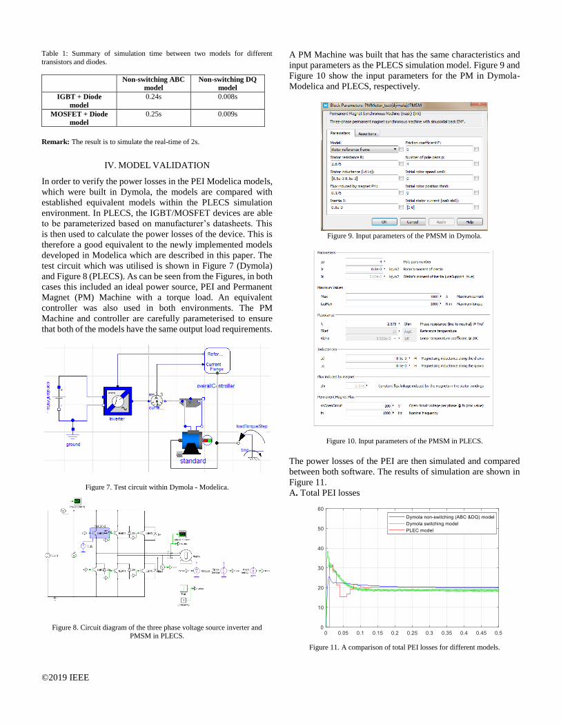
Table 1: Summary of simulation time between two models for different
transistors and diodes.
Non-switching ABC
model
Non-switching DQ
model
IGBT + Diode
model
0.24s
0.008s
MOSFET + Diode
model
0.25s
0.009s
Remark: The result is to simulate the real-time of 2s.
IV. MODEL VALIDATION
In order to verify the power losses in the PEI Modelica models,
which were built in Dymola, the models are compared with
established equivalent models within the PLECS simulation
environment. In PLECS, the IGBT/MOSFET devices are able
to be parameterized based on manufacturer’s datasheets. This
is then used to calculate the power losses of the device. This is
therefore a good equivalent to the newly implemented models
developed in Modelica which are described in this paper. The
test circuit which was utilised is shown in Figure 7 (Dymola)
and Figure 8 (PLECS). As can be seen from the Figures, in both
cases this included an ideal power source, PEI and Permanent
Magnet (PM) Machine with a torque load. An equivalent
controller was also used in both environments. The PM
Machine and controller are carefully parameterised to ensure
that both of the models have the same output load requirements.
Figure 7. Test circuit within Dymola - Modelica.
Figure 8. Circuit diagram of the three phase voltage source inverter and PMSM in PLECS.
A PM Machine was built that has the same characteristics and
input parameters as the PLECS simulation model. Figure 9 and
Figure 10 show the input parameters for the PM in Dymola-
Modelica and PLECS, respectively.
Figure 9. Input parameters of the PMSM in Dymola.
Figure 10. Input parameters of the PMSM in PLECS.
The power losses of the PEI are then simulated and compared
between both software. The results of simulation are shown in
Figure 11.
A. Total PEI losses
Figure 11. A comparison of total PEI losses for different models.

©2019 IEEE
Table 2. A summary of total PEI losses for different models.
Model Total PEI losses (W)
PLECS 20.991
Modelica non-switching (ABC &
DQ) model
20.668
Modelica switching model 19.732
From Figure 11, the results from PLECS model and Modelica
non-switching (ABC&DQ) model show nearly the same values
of the total inverter losses with only 0.3W difference. However,
there is a discrepancy during the initial start-up transient due to
the way of switching losses calculation. In the Modelica model,
it uses the peak load current while in the PLECS, it uses the
switching device. This has a little effect as it occurs during
transient (less than 0.02s). While the Modelica switching model
has the lowest total inverter losses and 2W difference from
PLECS model. This is due to the switching ripple exhibits in
the switching device, causing the miscalculation in the
averaging function. To minimize this ripple, a low pass filter
can be placed after the measurement of load current.
B. CPU time
Table 3. A summary of simulation time for different models.
Model CPU time (s)
PLECS 6.86
Modelica switching model 736
Modelica non-switching (ABC) model
0.083
Modelica non-switching (DQ)
model
0.0056
Table 3 shows that the Modelica non-switching DQ model has
the lowest CPU time, 0.0056s, while the Modelica switching
model has the highest CPU time, 736s. As expected, this shows
that the Modelica non-switching DQ model massively
improves CPU time over Modelica switching model. In
addition, the results show that the Modelica non-switching DQ
has significantly lower simulation times than both the PLECs
and Modelica ABC models. Considering the accuracy of the
DQ models, as detailed above, this huge decrease in
computational demand can be extremely useful when
simulating large systems or those which incorporate systems
within other physicals domains such as thermal or mechanical.
It can also massively decrease development time when multiple
simulations are needed for controller or filter tuning.
V. CONCLUSION
This paper has described the implementation of a newly
developed multi-level PEI modelling library in Modelica. Each
model has been described, including a new implementation of
switching loss modelling which gives accurate results in vastly
reduced simulation times. The results from simulation verified
the developed IGBT and MOSFET models with built-in diode
in Modelica. By comparison to established PLECS models, it
has been confirmed that the model can accurately calculate the
conduction losses and switching losses based on the
manufacturer’s datasheet.
V. ACKNOWLEDGMENT
This project has received funding from the Clean Sky 2 Joint
Undertaking under the European Union’s Horizon 2020
research and innovation programme under grant agreement
number 686783.
REFERENCES
[1] M. Helsper and N. Rüger, "Requirements of hybrid and electric buses - a huge challenge for power electronics," 2014 16th European Conference on
Power Electronics and Applications, Lappeenranta, 2014,pp.1-11.
[2] M. Richardson, "Hybrid vehicles — The system and control system challenges," UKACC International Conference on Control 2010,
Coventry, 2010, pp. 1-8. [3] B. Sarlioglu and C. T. Morris, "More Electric Aircraft: Review,
Challenges, and Opportunities for Commercial Transport Aircraft,"
in IEEE Transactions on Transportation Electrification, vol. 1, no. 1, pp. 54-64, June 2015.
[4] F. Casanellas, "Losses in PWM inverters using IGBTs", IEE Proc.-Electr.
Power Appl., vol. 141, No. 5, September 1994, pp. 235-239 [5] G. Su and P. Ning, "Loss modeling and comparison of VSI and RB-IGBT
based CSI in traction drive applications," 2013 IEEE Transportation
Electrification Conference and Expo (ITEC), Detroit, MI, 2013, pp. 1-7. [6] M. H. Bierhoff and F. W. Fuchs, "Semiconductor losses in voltage source
and current source IGBT converters based on analytical derivation," 2004
IEEE 35th Annual Power Electronics Specialists Conference (IEEE Cat. No.04CH37551), Aachen, Germany, 2004, pp. 2836-2842 Vol.4.
[7] Van der Linden, F., Schlegel, C., Christmann, M., Regula, G., Hill, C.I.,
Giangrande,P., Mare, J.C., Egaña, I. “Implementation of a Modelica Library for Simulation of Electro-mechanical Actuators for Aircraft
and Helicopters.” Proceedings of the 10th Inter-national Modelica
Conference. 2014.


![An approach to virtual-lab implementation using Modelica€¦ · vious work on this topic addresses the combined use of Modelica/Dymola and other software tools [11–13]: the virtual-lab](https://img.pdfslide.net/doc/110x75/5e926e058553e71458357889/an-approach-to-virtual-lab-implementation-using-vious-work-on-this-topic-addresses.jpg)