Embed Size (px)
Citation preview
Implementation of Closed Loop Feedback
Control of Piezoelectric Disc based Atomic Force
Microscope
Usman Ali Javid
Supervised by
Dr. M. Sabieh Anwar
Department of Physics
Lahore University of Management Sciences

Acknowledgements
A lot of people have contributed towards the completion of this project. Firstly, my parents have
provided me with constant motivation throughout the year and helped arrange so many trips to
Lahore. My friends and colleagues have kept my spirits high in times where I felt over-burdened
while managing the project in Lahore and classes in Islamabad. Thanks to Salman, Tabinda,
Abdullah Lodhi, Ansub, Hisham, Irteza and Asad Raza for keeping me on my toes with their
constant support and praise. Special thanks to Ahmer for providing support for fabricating
electronics for the project.
Dr. Mashhood Ahmad has been a mentor to me through the entirety of this endeavor. He has not
only helped me understand the theory of the project, but constantly guided me is developing
research skills and choosing a right path for my future studies. I have acquired a huge amount of
knowledge on topics of research in physics in his classes and under his supervision for this
project.
Special thanks to Physlab at the department of Physics, LUMS. Physlab is a unique team of
scientists and engineers specializing in research and development in experimental physics and
physics education. This project has been entirely funded by them and all the support and logistics
has been provided in full by Physlab. Thanks to Ali Akbar and Azeem for helping me out and for
providing a listening ear whenever I needed someone. Thanks to Dr. Usman for providing his
expertise in the field of microscopy. Thanks to Hafiz sahib, Khadim bhai and Ali Hasan for
providing hardware support and helping me streamline the project.
The work was originally started by Muhammad Wasif who is a former member of Physlab. He
laid most of the ground work for the mechanical and optical design and determining what
equipment were needed. He laid a very solid foundation on which I was able to build upon with
relative ease. He also has helped me after I took over the project and guided me in getting to
know the environment I would be developing the AFM in for the next year.
Ordinarily, this would conclude the acknowledgements but I cannot fathom going forward
without mentioning one name and that is Dr. Sabieh Anwar. He is the leader of Physlab and the
person behind this and many other high profile physics projects in the country. It is because of
him this project exists and has reached so many milestones over these years. Dr. Sabieh has
turned an idea of a home grown AFM into a reality. His knowledge of the subject and his insight
of design and engineering have no parallel. He has steered this project from scratch to its
completion and has provided me with all I have needed to achieve our goals. He has always been
there for me for any kind of help including technical, logistics, equipment, and has provided me
moral support at every turn. He has given me an environment full of research, scientific enquiry
and curiosity. I have learned an immense amount of knowledge from him and it is beyond any
doubt that I am a better scientist because of him. I will forever be in his debt.

DEDICATED TO
My Loving Mother

Abstract
In this project, we have developed an atomic force microscope (AFM) capable of resolving
vertical features of the order of 20 nm over an area of 12 microns square. This is achieved by
analyzing the reflection of a laser beam off a cantilever making contact with the surface of a
sample placed on a motorized transition stage driven by piezoelectric based nano-positioning
actuator. The reflected beam's position is monitored by a closed loop proportional-integral
control system that was specifically designed for this purpose. This AFM is a cost effective
solution for a very sensitive instrument that has become essential in today’s research and
development in Nanotechnology, Solid State Physics, Microbiology and many other fields of
Science and Engineering.

Contents
Chapter 1 Introduction
1.1 History of AFM 1
1.2 Working Principle of AFM 2
1.3 Setup of AFM 3
1.4 Applications 4
Chapter 2 Implementing AFM
2.1 Optical Assembly 9
2.2 Mechanical Construction 12
2.3 Electrical Construction 17
2.4 AFM Operation 21
Chapter 3 Feedback Control of AFM
3.1 Need for a Feedback Mechanism in AFM Operation 24
3.2 AFM Feedback Loop 24
3.3 Fundamentals of PID Control 26
3.4 Controller Tuning 27
3.5 Performance of AFM with PID control 29
Chapter 4 AFM Imaging
4.1 Generating AFM Images 33
4.2 Processing AFM Images 34
4.3 AFM Image Artifacts 36
4.4 Actual Images 39
4.5 Further Improvements and Future Directions 45
References 47
Appendices
Appendix A Software and Codes 50
Appendix B Hardware Support 55

1
Chapter 1
Introduction
1.1 History of Atomic Force Microscopy
For most part of scientific history, observing small objects has been done with optical
microscopy. Even today, for most practical purposes, these microscopes work effectively.
However the resolving power of this technique is cut short by the diffraction limit. In principle a
feature that has a size smaller than half the wavelength of illuminating light cannot be resolved.
Additional limitations are present due to imperfections of refractive material of the lenses
employed and aberrations in images. In the 1980’s, scientists started experimenting on a different
method to image samples indirectly by measuring the interaction of a small probe when placed
on the surface of the sample. This technique is called scanning probe microscopy (SPM).
Changes in this interaction could then be used as an image contrast with false colors. First among
this class of microscopes was the scanning tunneling microscope (STM) developed in 1982.
STM uses Quantum tunneling to create false color image by applying a potential across the
probe and the sample. This technique can provide atomic resolution but is limited to conducting
samples only. In 1986, another SPM technique was developed that used the atomic forces
between a sample atom and the probe to create an image. This came to be known as atomic force
microscopy (AFM). At distances beyond 1nm, atomic forces (van der Walls, Electrostatic,
capillary forces) take effect and cause the probe to bend in or away from the sample being
scanned.
SPM, though an invention of the modern age, has deep roots in how surface profiling has been
done in old days. The predecessor of the SPM was the stylus profiler described by Shmalz in
1929 [1], which used a sharp tip on the end of a small bar, to which was dragged along the
sample surface, and built up a map, or more often a linear plot, of sample height. This profiler
utilized an optical lever to monitor the motion of a sharp probe mounted at the end of a
cantilever. A magnified profile of the surface was generated by recording the motion of the
stylus on photographic paper. This type of ‘microscope’ generated profile ‘images’ with a
magnification of greater than 1000x. In 1950, Becker suggested oscillating the probe from an
optical lever design used for one of the early models of a surface profiler in the 1920s. This
profiler had a vertical resolution of approximately 25 nm [2]. However, a fundamental problem
with this sort of instrument persisted, notably that the probe touched the surface in an
uncontrolled way, which could lead to probe damage in the case of a hard sample, and sample
damage in the case of a soft sample. Either of these problems would reduce the fidelity of the
image obtained, as well as the achievable resolution. In 1971 Russell Young demonstrated a non-
2
contact type of stylus profiler [3]. In his profiler, called the ‘Topografiner’, Young used the fact
that the electron field emission current between a sharp metal probe and a surface is extremely
dependent on the probe sample distance for electrically conductive samples. This brings us to
1982, when Binning and Rohner at IBM used this tunneling current to create the first STM [4].
This led to the development of the AFM by measuring atomic forces rather than electrical
current to create topographical images of surfaces.
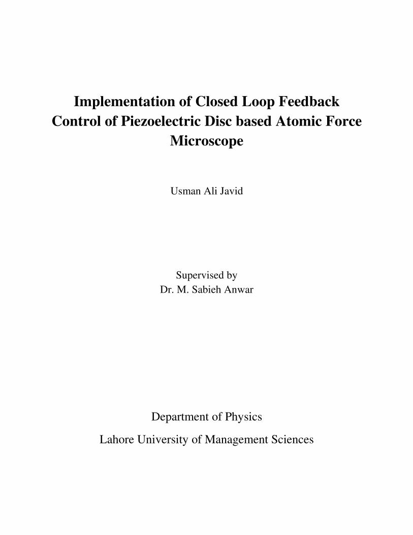
1.2 Working Principle of the AFM
Atomic forces between atoms are a function of the distance between them. This concept is
exemplified by the Lennard Jones potential function. This potential is developed due to atomic
forces between the atoms. Figure 1.1 show the potential plotted versus distance. Starting from a
long distance there is no appreciable force. As the distance decreases below 1 nm, an attractive
force produces negative potential in the atoms. Further decreasing the distance strengthens the
attraction. Due to Quantum effects in the form of Pauli repulsion, an opposite force is also at
play. In equation 1.1 the r12 term represents the repulsive force and the r6 term represents the
attractive part. This force-distance relation can be used to detect changes in separation between
the sample and probe caused by features on the sample’s surface.
Figure 1.1: Lennard JonesPotential. rm represents point of minimum potential.
���� � 4� � ��
�� (1.1)
In (1.1), σ is the distance at which the potential is zero and ε is the depth of potential well. This
equation can be used to determine small distances if the atomic force is known. The resolution of
this technique, among other things, will largely depend upon a way to achieve precise and
controlled motion of the probe on the sub-nanoscale level. This has been achieved by the
development of piezoelectric actuators that can make calculated movements in all axes.
3
This AFM technique produces three dimensional topological images with contrasts of false
colors representing height. This technique can also be used to determine properties such as
frictional coefficients, electrical conductivity magnetic properties and several other physical
characteristics along with chemical properties and identification of types of atoms present in a
given sample.
1.3 Setup of AFM
1. Cantilever with a sharp tip: The stiffness of the cantilever needs to be less the effective spring
constant holding atoms together, which is on the order of 1˗10 nN/nm. The tip should have a
radius of curvature less than 20-50 nm (smaller is better) and a cone angle between 10-20
degrees.
2. Scanner: The movement of the tip or sample in the x, y, and z-directions is controlled by a
piezoelectric tube scanner. For typical AFM scanners, the maximum ranges for are 80 mm x 80
mm in the x-y plane and 5 mm for the z-direction.
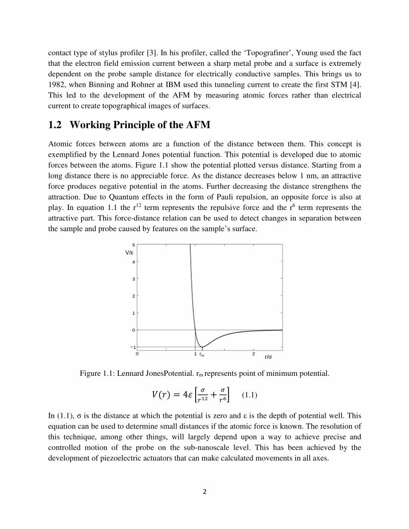
3. Detector: A transducer that can translate the motion of the cantilever into electrical signals.
The detectors used in AFM and their techniques are listed in the next section. Figure 1.2 shows a
general construction scheme of an AFM.
Figure 1.2: A general AFM assembly.
1.3.1 AFM Detection Techniques
Over the years many methods have been used to measure the deflection on the cantilever. They
are:
1. Laser beam deflection: the surface features can be quantified by measuring the change
in reflection angle of a laser beam focused on top of the cantilever. This technique is
called the optical lever and is most commonly used

4
2. Interferometry: The reflection of the laser beam off the cantilever is made to interfere
with an undeviated beam in a standard Michelson interferometer setup. The movement of
the interference fringes gives the measure of surface features that cause the cantilever
deflection [5]. This method, unlike the previous one, needs a check to determine the
direction of motion since both up and down motion can cause similar changes in the
position of the fringes.
3. Capacitive Transducers: Capacitive sensors can be used with one end attached to the
probe and the other with the sample. These sensors communicate the distance in terms of
changes in their capacitance. This method has a very high sensitivity but it is costly and
requires an additional cumbersome mechanical assembly.
1.3.2 AFM Operating Modes
AFM can be operated in several ways. The image data can be extracted if the cantilever is in
repulsive region of the force distance curve of the attractive. The tip may or may not be driven at
a frequency. The different modes of AFM are summarized in this section.
1. Contact mode: The cantilever tip is physically in contact with the sample. The tip moves
over the surface keeping a constant distance and thus imaging surface features. This
mode gives the best resolution but due to dragging, can damage soft samples. This
method is not recommended for biological samples
2. Tapping mode: The cantilever is driven at near its resonance frequencies. Changes in
height alter the amount of force experienced by the oscillating probe which is translated
in its amplitude and frequency.
3. Non-contact mode: The cantilever hovers over the sample surface at a very small
distance. The distance is kept such that the interaction is in the attraction region of the
force-distance curve. Changes in distance produce bends in the probe which can then be
measured.
1.4 Applications
Although AFM, via STM, had its origins in imaging of metals and semiconductors, it was
originally invented in order to be able to extend the possibilities of STM to other samples, in
particular biological samples. AFM’s ability to image a wide variety of samples, coupled with its
simplicity of operation and the relatively low cost of the instruments, means that AFM very
quickly gained acceptance in an extremely wide range of fields. AFM today has so many
applications that the huge diversity cannot possibly be addressed. Here some of the most widely
used applications that AFM has today are discussed.
5
1.4.1 Applications in Physics and Material Science
Fundamental applications in physical sciences include imaging of the fine structure of metals and
absorbed species on metals and semiconductors; although this is one area where STM is still
more widely applied than AFM, some parameters revealed by AFM can under some
circumstances surpass STM. AFM imaging is highly suitable for structural studies of inorganic
and organic insulators and has been widely applied.
Surface Roughness at the Nanoscale
Surface roughness is easy to measure with AFM, due to the fact that AFM produces high
contrast on relatively flat surfaces, and produces three-dimensional, digital data by default. AFM
gives accurate values for surfaces with roughness down to the level of atomic flatness [6].
Therefore, AFM has become the method of choice to measure nanoscale roughness, and is
routinely applied to determine roughness of metals and metal oxides, semiconductors, polymers,
composite materials, ceramics, and even biological materials.
Atomic resolution Imaging of Crystal Structures
The AFM at its atomic resolution allows researchers to observe the atomic structure of a large
number of metals, semiconductors, metal oxides, and multi-layered structures [7, 8, 11]. This
technique can even reveal sub-atomic detail, e.g. information of molecular orbitals can be
determined in some cases [29]. Many atomic-resolution images produced by AFM are produced
by non-contact-mode AFM (using FM detection), and often carried out in high-vacuum
conditions [10].
Friction Measurements
Lateral force microscopy (LFM), or friction force microscopy, is applied for many purposes. For
example: fundamental study of tribology of macroscopic or atomic scale systems, determination
of the friction properties of materials or their characterization [9]. Applications include studies of
monolayers, including the friction between monolayers on the probe and on a sample surface
[12], friction-based discrimination of phases in polymer blends [13] and discrimination of
inclusions in heterogeneous polymer surfaces, and friction studies of carbide coatings for tool
coatings. The ability of LFM to discriminate different chemical groups means that it can be used
to study phase separation in mixed monolayers [14], and is very commonly used to detect
directly deposition of features by dip-pen nanolithography or nanografting, because the contrast
is often better than in the height image.
Magnetic Domain Mapping
Magnetic Force Microscopy (MFM) is a variant of the standard AFM with a magnetic metal
coated on the tip of the probe. This specifically allows the measurements of magnetic forces.
MFM can create contrast in images based on magnetic activity in the sample. Therefore it is a
6
very useful tool for imaging magnetic domains in magnetic materials and performing related
measurements [15].
1.4.2 Applications in Nanotechnology
Imaging Nanoparticles and Nanotubes
Nanoparticles are probably the most widespread nanostructures, and over the last 10 years or so
there has been an enormous increase in the interest in their production due to their unique
properties. It is extremely important to have a tool to characterize with extreme accuracy the size
of such particles. The AFM is capable of providing more information than just topography, and
many other properties of nanoparticles have been probed in recent years [16, 17]. AFM can be
used to measure an extremely wide range of nanoparticles including different metal
nanoparticles, metal oxide particles, many types of composite metal/organic particles, synthetic
polymer particles, biopolymer nanoparticles, nanorods and quantum dots [18] etc.
The mechanical properties of pseudo one-dimensional (1-D) materials such as nanotubes,
nanowires, nanorods, nano belts, etc. are the subject of great interest. However, making
mechanical measurements of individual nanofibres is extremely difficult, mainly due to the
difficulties in locating the objects and fixing them to the testing devices. AFM is ideal for this
task, as it can perform both imaging and manipulation of the nanostructures. Furthermore the
high positioning accuracy makes it possible to mechanically probe objects having dimensions of
less than 10 nm easily [19]. For this reason AFM-based techniques have been widely applied to
mechanical measurements of 1-D nanostructures.
Nanodevice Construction
Nanomanipulation, involves assembling tiny building blocks (atoms and molecules) directly, one
at a time. Highly complex structures can be formed with this technique. AFM-based systems are
well suited to this sort of task, due to the possibility to move the probe with sub-nanometer
accuracy. An additional advantage of AFM for this task is the ability to use the instrument as a
sensor as well as the manipulator. For example, an AFM-based nanomanipulator with a haptic
interface can be used to move carbon nanotubes onto micron-scale electrodes in order to measure
their electrical properties [20]. Various biological nanostructures (e.g. DNA, chromosomes, etc.)
have been manipulated using AFM probes.
Nanoparticle-DNA interactions
One of the most important areas of nanoscience is Nano bioscience, which can be defined as
exploiting nanotechnology to solve biological problems. Within Nano bioscience, probably the
most widely applied technology in the medical biosciences is that of nanoparticles, which have
been used and proposed for a variety of diagnostic, imaging and treatment strategies.
Nanoparticles are almost the sizes of viruses or even of individual proteins, and thus may interact
7
with the targets as would proteins and viruses. AFM is an ideal technique to directly observe the
interaction of nanoparticles (which are usually based on a metal or crystalline semiconductor)
with their biomolecule targets [21].
1.4.3 Applications in Biology
Bimolecular Imaging
Biomolecules form the basis of life, and understanding the structure, function and interactions of
biomolecules has been the key to the incredible progress in the life sciences, and medicine in
particular. As a technique with sub-molecular resolution and the ability to image soft samples in
water, AFM is highly appropriate for the study of a huge range of natural biomolecules. AFM is
for example particularly suitable technique for protein studies [22], due to the coupling of high
resolution with the ability to study samples under physiological conditions, which is necessary
because a protein structure can be highly sensitive to the nature of the proteins’ environment.
Nucleic acids are also highly suited to AFM imaging, and can be imaged in air and in liquid, and
by contact, non-contact and intermittent-contact modes. Samples have included single stranded
DNA, double stranded DNA and ssRNA in an extended configuration have been imaged [23].
Bacterial Cell Measurements
AFM is a highly suitable tool to examine bacteria, and has been widely applied for this purpose.
Bacteria are commonly studied by optical microscopy, which can give an overall idea about
gross cell morphology, and is also useful for cell-counting studies. In comparison, AFM is
slower, and thus is less useful for quantitative cell-counting, but allows measurement of a variety
of other cellular properties, particularly by nanoindentation and force spectroscopy experiments
[24]. In addition, the greatly increased resolution of AFM allows for the imaging of finer details
of cell morphology and sub-cellular features.
Biological Force Spectroscopy
For the interactions of biological molecules, AFM has some unique advantages. It is very
sensitive, allowing the interactions between single pairs of molecules to be studied due to force
resolution in the 10 pN range. Moreover, it can be very selective. The control over the x, y and z
position of the probe with immobilized molecules means that unlike most techniques, by AFM-
based force spectroscopy, it’s possible to control exactly which molecules interact, and where
they are doing it [25].

8
Chapter 2
Implementing the AFM
This chapter explains the entire structure and design of Physlab’s AFM with details on electrical
circuitry, data connections, power and signal flow, optics and mechanical design. The AFM
project is truly multidisciplinary in nature consisting of an optical assembly along with
electronics to drive the data flow and a mechanical setup to support and actuate the system.
Figure 1.1 provides the overall design of the AFM with arrows indicating data flow. All
information is acquired by the computer through a data acquisition device. The computer also
processes the data to generate AFM images.
Figure 2.1: AFM flow diagram.
A National Instruments Data Acquisition Board (PCI-6221) is used as the data acquisition
device. It is interfaced with a photodetector and an Arduino based microcontroller which will
later be used for feedback. The DAQ board also performs the core function of driving the AFM
actuator. A LabVIEW program generates the driving signals for the actuator and processes the
acquired data from the photodetector. Not involved in the main data flow loop is a CCD Camera

9
arranged in a digital microscopic arrangement using a 3x microscope objective lens and a
precision stepper motor. These two devices are controlled directly by the CPU and are essential
for proper functioning of the AFM as will be explained later.
A set of analog electronics control and maintain the data flow and power up the equipment. They
are involved in conditioning the data to suit each interfaced component of the AFM. The detailed
schematics and working of the electronics are discussed later throughout this chapter. The data
from the AFM requires substantial post-processing and we use Matlab for creating the image and
a readily available Image processing program “Gwyddion” for processing. The final output is a
processed image with measurements of the objects in the field of view.
2.1 Optical Assembly
Central to the AFM operation is its optics. Fundamentally an AFM requires a light source, a
reflecting probe and a detector capable of measuring change in the reflection angle. A 635nm
1mW Diode Laser is used in the AFM. The laser is collimated with an aspheric lens and then
focused sharply onto the top surface of a probe. The power of the light beam after reflection off
the probe is measured to be 15uW. The loss of optical power is due to the fact that the focusing
lens, despite proper adjustments, cannot make the laser point shorter than the surface of the
probe and so, some light is not reflected. Figure 2.1 shows the optical path that the laser takes in
the AFM.

10
Figure 2.2: AFM optical assembly.
The lenses are placed inside a lens tube which is attached to the diode laset. Also the CCd camera is
attached with the objective lens through a similar lens tube. Both elements have adjustment knobs on
them to make precise adjustments to the direction and focus of the laser and the fiel;d of view of the
camera.
2.1.1 AFM Probe (Cantilever)
A cantilever is the probe used for scanning the surface that needs to be imaged. A Silicon-nitride
probe has been employed in the construction. It has a 31nm pyramidal tip at its bottom. The top
surface is gold plated to get good reflection. The entire probe is 220µm long and two of these
probes are mounted onto a cantilever of rectangular shape as shown in figure 2.3. Note that the
tip is non-magnetic and can only be used to image surface topology.
Figure 2.3: cantilever observed through (a)digital Microscope and (b) through CCD microscope.
The cantilever is held in place by a cantilever holder with a clip that firmly grips the probe. The
cantilever is flexible and can bend towards and away from the surface of the sample depending
upon the atomic force it experiences. The cantilever is a sensitive element and can easily break.
So care is taken while loading the cantilever and the process is done under a stereo microscope
with special soft edged tweezers.
The cantilever is held by the holder in such a way that it makes an angle with the horizontal. This
can be seen in figure 2.2. The laser is shone vertically onto the probe and the reflected beam falls
on a photodetector placed in front of the cantilever. By simple geometric calculations, it can be
shown that any change in the angle of the cantilever creates a change in the reflection angle of
the laser twice its magnitude.
2.1.2 Lenses and Tubes
A pair of lenses is present in the path of the laser. The first is an aspheric lens of focal length 1.2
mm. It is used to collimate the light being emitted by the diode. Another lens of focal length 50

11
mm focuses the light sharply on the surface of the cantilever. The lens is adjusted so that the
cantilever is present exactly at its focal point. Both of these lenses are mounted inside a hollow
lens tube. A 3x microscope objective connected with a CCD camera is also present to serve as a
digital microscope to view the AFM operation and make sure the laser is hitting at the right spot.
This microscope has a field of view of approximately 1 x 2 µm.
2.1.3 Photodetector
The AFM requires an unusual type of detector that measures the reflection angle of a light beam
in addition to its intensity. The detector used in our work is a Thorlabs PDQ80A Quadrant
Position Sensing Detector (PSD). It consists of four quadrants of photosensitive semiconductor
material. The detector can identify changes in the horizontal and vertical direction by measuring
intensities in each quadrant using these formulae for determining normalized coordinates of the
laser represented by Xp and Yp.
Figure 2.4: Quadrant photodetector.
The normalized Xp and Yp coordinates of a laser spot in the surface of the detector are given by
equation 2.1.
�� � ���������������� �� � ���������
������� ……….. (2.1)
The photodetectror performs a current-to-voltage conversion with its in-built trans-impedance
amplifiers with a gain of 10KV per ampere. Its nominal sensitivity at the 635nm wavelength is
0.4A per watt of optical power. A three channel analog output provides the coordinates x, y and a
sum of the intensities at each quadrant. Manipulating this data can also give diagonal variations
in beam’s position.
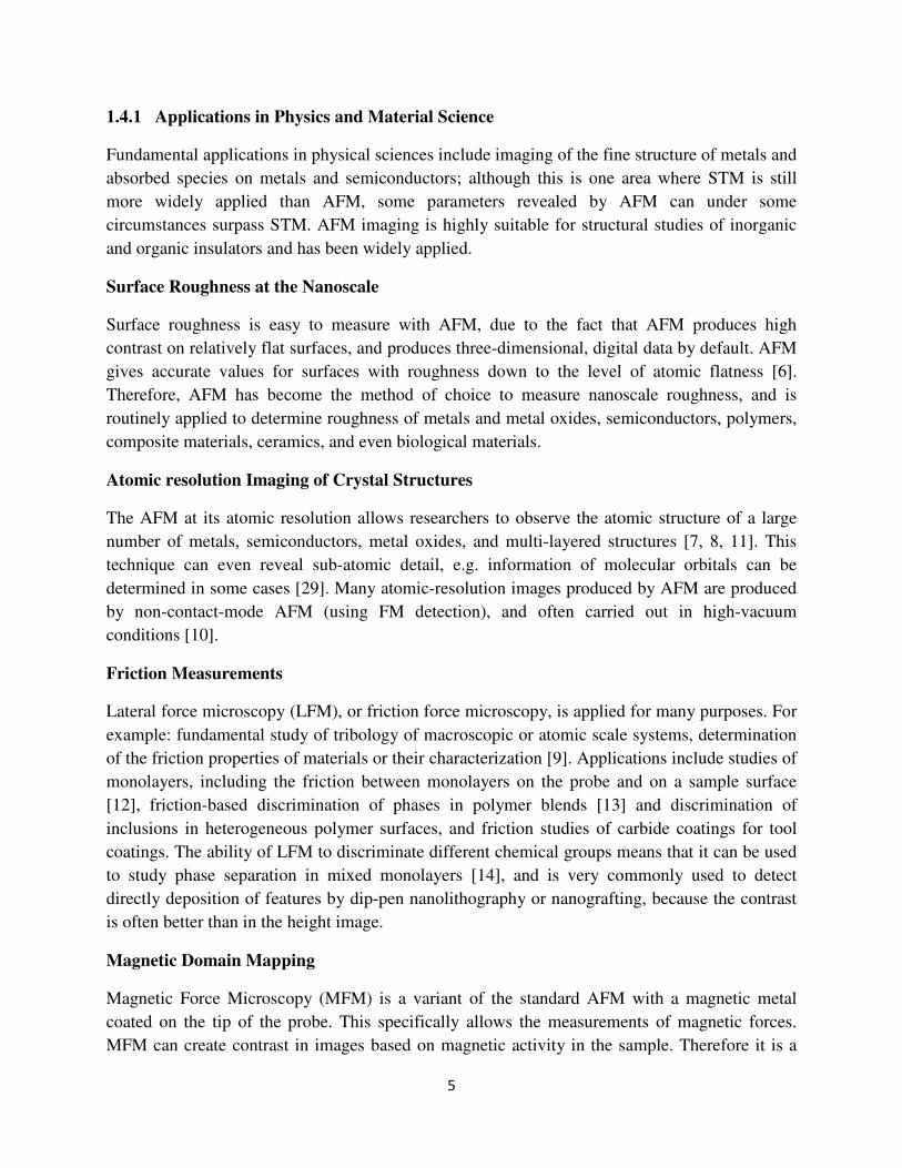
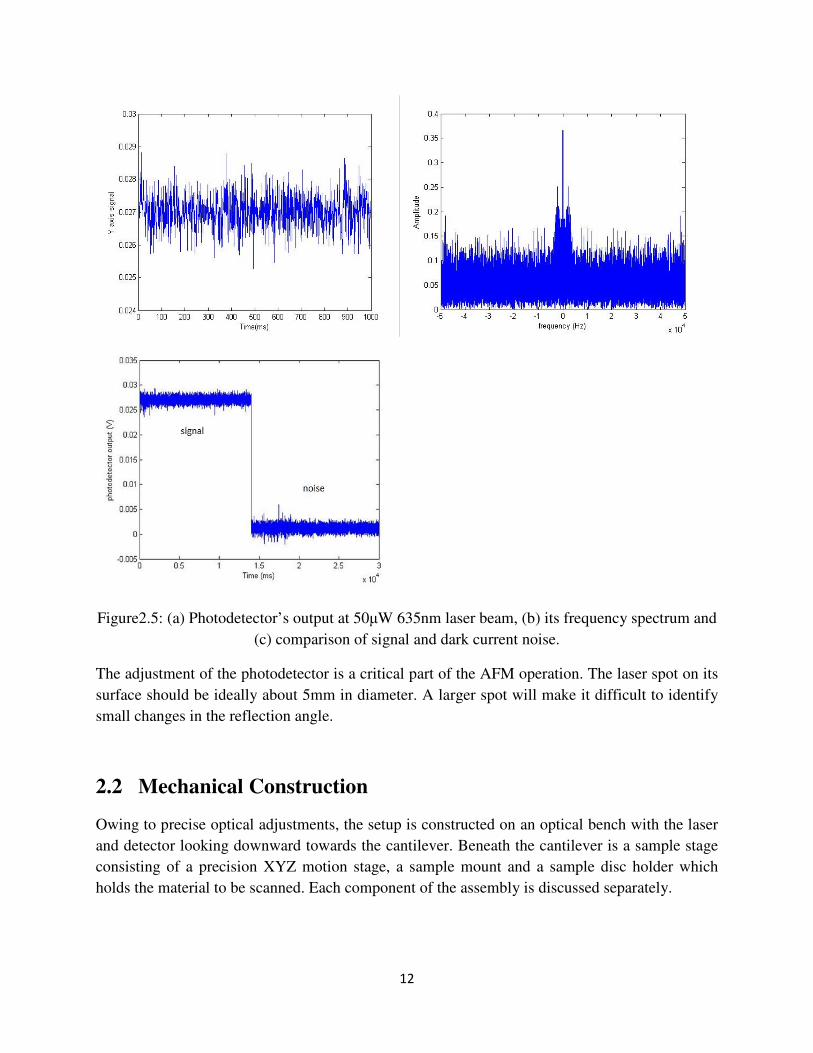
Figure 2.5 shows the output of the quadrant detector when incident with a 635nm 50uW laser.
The dark current was also observed and plotted. This data is used to calculate the Signal to Noise
Ratio (SNR) of the detector which will later give a measure of uncertainties in the measurement
of image features.
12
Figure2.5: (a) Photodetector’s output at 50µW 635nm laser beam, (b) its frequency spectrum and
(c) comparison of signal and dark current noise.
The adjustment of the photodetector is a critical part of the AFM operation. The laser spot on its
surface should be ideally about 5mm in diameter. A larger spot will make it difficult to identify
small changes in the reflection angle.
2.2 Mechanical Construction
Owing to precise optical adjustments, the setup is constructed on an optical bench with the laser
and detector looking downward towards the cantilever. Beneath the cantilever is a sample stage
consisting of a precision XYZ motion stage, a sample mount and a sample disc holder which
holds the material to be scanned. Each component of the assembly is discussed separately.

13
2.2.1 Precision XYZ motion stage
A Newport ULTRAlign Precision XYZ Linear Translation Stage is at the center of the assembly.
It has coarse micrometer level adjustments for X and Y axis and a place to attach a precision
motor for Z axis motion. The stage allows controllable linear motion in all axes making it easy to
adjust the sample that needs to be scanned.
Figure 2.4: Newport Precision XYZ motion Stage.
At the top of the stage is placed a magnetic iron cylinder which serves as the sample mount and
holds a magnetic sample disc.
2.2.2 Precise Z axis Motion
In order for the AFM to begin operation, the tip needs to be engaged with the surface of the
sample. This is an extremely delicate process and requires a slow controlled upward motion of
the sample. For this purpose a precision motor is used for a nano-scale Z axis motion.
A Newfocus Picomotor is used for controlled Z axis motion of the stage. This motor can produce
a minimum step of size shorter than 30nm. When a sample is mounted and aligned, the motor
brings it close enough to the tip that the atomic forces come into play. Thus motor plays the role
of adjusting the point of operation on the force distance curve (figure 1.1).

14
Figure 2.5: New Focus picomotor.
2.2.3 Piezoelectric Actuator
The advent of piezoelectric materials has made possible applications that require nano-scale
motion. They have played a central role in the development of scanning probe microscopy and
eventually the AFM. Traditionally an AFM uses a three dimensional tube made from
Piezoelectric material specifically fabricated for this purpose. Such actuators are pre-calibrated
from the manufacturer and make up a large percentage of the total cost of the microscope. Since
one of the main objectives of this project is to cut the cost it takes to build an AFM, a non-
conventional actuator is used.
Piezoelectric discs are commonly used in buzzers since they can vibrate with amplitudes in sub-
micrometers. This ability is exploited to turn this disc into an actuator which functions thus:
• A voltage difference created horizontally causes sideways motion of the disc which
moves in a bow-like manner
• A voltage difference applied between the top and bottom surface causes the disc to rise
and fall at the center causing a linear z axis motion. These types of motion are shown in
figure 2.6.

15
Figure 2.6: Nano-scale Motion with Piezoelectric Discs. Image taken from [5].
To make this happen, a metallic plate on the top surface of the piezoelectric disc is sliced into
four quadrants and each of these is connected to the driver electronics. Since motion in all three
axes is required, another piezoelectric disc is stacked beneath this disc. The lower disc is used for
motion in Z axis with two electrodes connected to its top and bottom surface. This complete
actuator is then placed on the motion stage under a metallic plate with a circular opening at the
center to provide space to place the sample holder. Figure 2.7 shows a schematic of the piezo
actuator assembly.
Figure 2.7 Piezo actuator setup.

16
2.2.4 Levels of motional adjustment
To sum up, there are three levels of notional adjustments that can be made to the AFM.
1) Coarse Adjustment: The motion stage provides micrometer level adjustments in the x-y
direction with its two screw gauges.
2) The Precision Picomotor provides a very fine z axis adjustment on the order of
nanometers
3) The Piezoelectric disc provides sub-nanometer precise motion in all three axes.
All of these degree of freedom play a role in setting the AFM’s tip-sample interaction in a
desired region on the force distance curve. For contact mode scanning this region is the repulsive
linear region on the curve.
Figure 2.8: attractive and repulsive regions on the force-distance curve.
2.3 Electrical Construction
The electronics on the AFM provide power to its components, generate signals to drive its
actuator and condition signals for analysis of the data. The block diagram in figure 2.9 shows the
parts in this construction and each is then discussed in detail.

17
Figure 2.9: Electrical Construction Flow Diagram.
2.3.1 Power Supply
Piezoelectric materials require large driving voltages to operate. For this purpose a ±50V bipolar
power supply is made. The power supply is standard in its construction with a step down
transformer followed by a rectifier and filtering capacitors. This supply however is special in two
ways. First the output of the rectifier is floating i.e. without reference to ground. This is essential
to make this a bipolar supply. Secondly, Since the AFM output data is quite weak (in millivolts)
and sensitive with important data in the second and third decimal place of the photodetector
output; the power supply is regulated after the filtering stage to remove any ripples. For this
purpose LM317 (positive voltage regulator) and LM 337 (negative voltage regulator) are used.

18
Figure 2.10: 100V bipolar power Supply.
2.3.2 X-Y axis Piezo Driver
The heart of the electronic design is the driver for the piezoelectric discs. To do a raster scan of a
sample, triangular signals are used. Two such signals are generated from the DAQ board using
the LabVIEW interface. One is a slow negative sloping linear signal that drives the Y axis slow
scan. The other is a Triangular wave of a higher frequency that drives the fast X axis scan.
Together these two signals create a raster scan pattern as shown in figure 2.11.
Figure 2.11: Raster scan pattern that drives the piezoelectric disc.
The electronics for the X and Y axis scan consist of two high voltage amplifiers (OPA445).
These amplifiers pick the slow and fast scan signals and amplify them to 80V peak-to peak (or
±40V) triangular waves. These signals are then transferred to the four quadrants of the X-Y
Piezo disc. The amplifiers are set in standard non-inverting configuration.

19
Figure 2.12: X-Y driving signal amplification circuit.
2.3.3 Z Axis Piezo Driver
This is different than the X-Y piezo driver because the driving signal comes from the
microcontroller based on the feedback error. The microcontroller’s DAC is connected to an
OPA445 amplifier which turns the unipolar 0.55V˗2.75V DAC signal to ±40V amplified bipolar
voltage. The output pins are connected to the upper and lower side of the Z axis Piezo disc.

20
Figure 2.13: Z axis signal amplification circuit.
2.3.4 Signal Conditioning for Feedback
The output of the photodetector remains within a ±250mV range. This takes only a small part of
the microcontroller’s ADC range. To increase resolution it is desirable to amplify this signal. The
signal also needs to be converted into a unipolar signal since the ADC cannot read negative
voltages. To accomplish this, a two-stage amplifier circuit is constructed. The first stage consists
of an ultra-low noise precision operational amplifier LT1028. This IC is specifically designed for
amplifying low voltages. This IC’s noise performance is extraordinary with only 35nV peak-to
peak noise at 10Hz. LT1028 amplifies the signal to ±3.3V without adding any noise and thus
preserving the data.
The second part consists of an LTC2057 operational amplifier. This is also a low noise amplifier
and converts the ±3.3V signal to a unipolar 0˗3.3V signal. The entire process could be done in
one stage but giving offset requires providing a reference voltage which will always have some
noise in millivolts destroying the original data. The two stage configurations gives necessary
amplification and offset for the ADC of an Arduino Due board. The 3.3v reference signal is
picked up from Arduino board’s own 3.3V regulator output pin.

21
Figure 2.14: Signal conditioning circuit showing amplification and positive offset imparted to
photodetector’s Yp signal.
2.4 AFM Operation
2.4.1 Generating X-Y Scan Signals
The X-Y piezo disc has to move in a raster scan pattern. Motion along X axis is slow and the
disc sways from one end to another while the y axis motion is fast. The slow scan determines the
total scan time and the fast scan determines the resolution and pixel pitch in the final image. Two
triangular waves are generated for each scan axis. For a scan size of m-by-n microns, the x and y
axis resolution in micrometers is given by:
�� � ����� !�
…….. (2.2)
�" � #� $%&��� !
……. (2.3)
Where '()*+ and '�,(- is the frequency of the slow and fast scan signals respectively and '( is the
sampling frequency of data acquisition. It is always desirable to have both resolutions equal to
get pixels with an even pitch. This calculation is assuming a noiseless signal. However, the
actual resolution is lower due to noise and the creep response of the piezo disc to driving signals.

22
Figure2.15: (a) X fast scan signal and (b) Y slow scan signal produced by DAQ.
The two triangular signals are generated by the NI DAQ analog output terminals with amplitude
of 10V. The signals are then amplified by the OPA445 amplifiers discussed before to amplitude
of 40V. These signals then drive the disc to few microns in both axes. The true scan area is
determined by scanning a calibrated sample which will be discussed later.
2.4.2 Scanning Images
After testing signals for X Y and Z axis motion along with the photodetector’s response, the
AFM is in a position to scan samples. Preparing the AFM for a scan requires some steps which
are now discussed.
1) Powering On: There are three power inputs for the AFM; one for the diode laser, one for
the Picomotor and one to power up the electronics. All must be powered on and in stable
state before the subsequent steps.
2) Adjusting Photodetector Position: The photodetector should be placed so that the laser
spot hits its center and is not more than 9mm in diameter. To do this, the photodetector is
moved first vertically and then horizontally to make sure both the Xp and Yp signals are
centered at 0V on the LabVIEW graphs.
3) Engaging the tip: The process of bringing the probe tip to the sample surface so we can
scan images and measure forces is called “engaging.” The aim is to get the tip in close
proximity so it is just barely coming into contact without bending. If the probe does not
touch the surface, it is obviously useless, but if it’s bent too much against the surface, it is
equally useless. The tip is carefully brought near the surface, first turning the motor knob
by hand, then very slowly with the Picomotor controls on the LabVIEW user interface.
When contact is made, the Y axis signal steeps upward. At this point the motor is stopped
and reversed very slowly to bring the cantilever to its original position so that there is no
bending. Due to adhesive forces, the tip would remain in contact even if the motor is
brought down further but that is not required.

23
4) Generating X-Y actuating signals: After contact is made, the two triangular signals are
applied from NI DAQ board with calculated frequencies for a particular image size. For
example a slow and a fast scan frequency of 0.005 Hz and 0.5 Hz at a sampling rate of 1
KHz will produce an image of size 1000x1000 in 1000 seconds with pixel pitch given by
equations 2.2 and 2.3.
While engaging the tip, measuring the cantilever deflection gives the force distance curve. This
curve lies in the core of AFM imaging and it is essential to know where the tip is on this curve.
For contact mode scanning, the tip should be in the repulsive region which appears just after
contact. This region is somewhat linear and a good signal swing can be obtained. Non-contact
mode scanning uses the attractive region of the curve. This technique, although more advanced,
provides less resolution and sensitivity than contact mode. A typical force distance curve
obtained is shown in figure 2.16.
Figure 2.16: A typical force-distance curve.
Before a complete raster scan can be done, scanning a line on the sample provides good
information about the piezo disc motion and detecting features on the sample’s surface. In the
line scan a bow-like motion is visible. This is due to the fact that the X-Y piezo disc does not
move linearly but sways from left to right making a bow. This creates an artifact in the image.
Following the step by step procedure of image scan, we have obtained several images. The data
comes sequentially in the form of a vector. Using Matlab, an image matrix is created by
comparing X-Y piezo driving signal with the vector. The matrix is then converted into a
grayscale image. This image is raw and contains numerous artifacts which obscure the true
surface topology. Often nothing is visible at this stage. The raw image is passed through image
processing algorithms. The steps with details are described in chapter 4 of this dissertation.

24
Chapter 3
Feedback Control of AFM
3.1 Motivation for Feedback Control in AFM Operation
The mechanics of AFM operation that have been discussed so far are termed as “Open Loop” i.e.
a one-way process where a system is given an input and it generates an output purely depending
upon its nature regardless of any constraint placed by the user. The data flow is in uni-direction
as opposed to a feedback. The system in this case is the cantilever being deflected off the
sample’s surface. The amount of deflection is not being monitored or controlled and the system
is free to react to the stimulus. This is how all systems behave naturally when there is no
constraint on their output.
Ideally an open loop mechanism is fine for the AFM to generate data however the reliability of
this data can be an issue if the laser is not falling properly on the photodetector’s sensitive
surface. The PDQ80A Quadrant detector has a circular surface of 12mm diameter. For samples
with large height features, the laser goes off the surface. This limits the AFM to scanning small
samples. The particular setup is capable to manage samples with features up to 500nm. In order
to increase this range and get better results for large samples, a feedback mechanism is necessary
which continuously monitors the output and provides feedback to the user which then can be
used to adjust the assembly in real time so that the laser always shines within the detector’s
photosensitive part. Feedback control enhances the resukts ordinarily obtained in open loop
besides providing reliable operation [26].
3.2 AFM Feedback Loop
The feedback mechanism consists of the system that needs to be controlled, a sensor which is the
quadrant photodetector and a controller which analyzes the difference between the output and the
required response and calculates the necessary input that needs to be given to the system to get
the desired response. The system in this case is a piezoelectric disc which moves up or down in
nanometers based upon the voltage applied across its top and bottom surfaces. Figure 3.1 shows
a typical response of the disc in open loop for different voltages.

25
Figure 3.1: Response of Piezo disc to different voltages.
The controller being used is an Arduino Due board with a 32 bit ARM processor along with 12
bit ADCs and DACs. The processor runs at 84MHz which is more than what is needed. This is
the only Arduino board which produces a pure DC output from two 12 bit DACs. All other
boards generate a pulse width modulated signal when an analog output command is called. The
control loop consists of the controller generated controlled output based on the feedback which is
the y-axis (Yp) signal of the photodetector. The output then drives the sample up and down
ensuring that at all time the laser stays at the same point on the detector’s surface.
Figure 3.2: AFM feedback loop. Photo taken from [27].

26
A PID controller is the most common algorithm for feedback control. The theory and implementation of
this algorithm are discussed here.
3.3 Fundamentals of PID control
A proportional-integral-derivative or PID controller is a control system that uses the difference
of the output from a desired set point and calculates the necessary input to the system using the
error, its derivative and integral over the past values. PID controllers have been hugely
successful in all applications from industrial machinery to aircraft autopilot systems. The control
equation for a PID controller is given by:
.�/� � 0� 01 23�/�4/ 0556�-�5- ………. 3.1
Where Kp is the proportional gain, Ki is integral and Kd is derivative gain.
3.3.1 Proportional Response
The proportional component depends only on the difference between the set point and the
process variable. This difference is referred to as the error term denoted by E(t). The proportional
gain (Kp) determines the ratio of output response to the error signal. For instance, if the error
term has a magnitude of 10, a proportional gain of 5 would produce a proportional response of
50. In general, increasing the proportional gain will increase the speed of the control system
response. However, if the proportional gain is too large, the process variable will begin to
oscillate. If Kp is increased further, the oscillations will become larger and the system will
become unstable and may even oscillate out of control.
3.3.2 Integral Response
The integral component sums the error term over time. The result is that even a small error term
will cause the integral component to increase slowly. The integral response will continually
increase over time unless the error is zero, so the effect is to drive the steady-state error to zero.
The steady-state error is the final difference between the process variable and set point. A
phenomenon called integral windup results when integral action saturates a controller without the
controller driving the error signal toward zero.
3.3.3 Derivative Response
The derivative component causes the output to decrease if the process variable is increasing
rapidly. The derivative response is proportional to the rate of change of the process variable.
Increasing the derivative gain (Kd) parameter will cause the control system to react more strongly
to changes in the error term and will increase the speed of the overall control system response.
Most practical control systems use very small derivative gain (Kd), because the derivative
response is highly sensitive to noise in the process variable signal. If the sensor feedback signal

27
is noisy or if the control loop rate is too slow, the derivative response can make the control
system unstable.
3.4 Controller Tuning
The process of setting the optimal gains (Kp, Ki and Kd) to get an ideal response from a control
system is called tuning. There are different methods of tuning of which the “guess and check”
method and the Ziegler Nichols method will be discussed. The gains of a PID controller can be
obtained by trial and error method. In this method, the I and D terms are set to zero first and the
proportional gain is increased until the output of the loop oscillates. As one increases the
proportional gain, the system becomes faster, but care must be taken not make the system
unstable. Once P has been set to obtain a desired fast response, the integral term is increased to
stop the oscillations. The integral term reduces the steady state error, but increases overshoot.
Some amount of overshoot is always necessary for a fast system so that it could respond to
changes immediately. The integral term is tweaked to achieve a minimal steady state error. Once
the P and I have been set to get the desired fast control system with minimal steady state error,
the derivative term is increased until the loop is acceptably quick to its set point. Increasing
derivative term decreases overshoot and yields higher gain with stability but would cause the
system to be highly sensitive to noise.
3.4.1 Zeigler Nichols Method
The engineering team of Ziegler and Nichols developed this method in the early 1940’s. It is a
heuristic tuning method that gives extremely good values for controller gains by achieving
“quarter wave decay” which is a condition where the amplitude of oscillation drops to one-fourth
of its value in the previous cycle after a disturbance is recorded.
Figure 3.3: Quarter wave decay condition exemplified.

28
To achieve quarter wave decay, Zeigler came up with the following method
1) Initially keep Ki and Kd at zero and start increasing Kp form zero. The response will start
to take shape.
2) Increase Kp until the response of the system becomes oscillatory and the output has a
steady sinusoidal response. This value of proportional gain is called the critical gain Kc.
Note time period Pc of the oscillation and Kc.
3) Use the table below to calculate all the parameters of the controller
Control Mode Kc Ti Td
P 0.5Ku --- ---
PI 0.45Ku Pc/1.2 ---
PID 0.6Ku Pc/2 Pc/8
Table 3.1: Formulae for Zeigler Nicholes method.
Finally, the controller gains are given by these relations:
0� � 07 01 � 9:;<05 � 9:
;= ………… 3.2
3.4.2 Tuning Controller Gains for the AFM
This method was employed for the AFM to tune the controller parameters. Before designing the
controller, it is very important to observe the system’s step response to see the stability of the
system. This helps in determining what kind of controller (P, PI, PID PII) will be needed. Figure
3.4 shows the step response of the Z axis piezoelectric disc. A square wave signal with amplitude
of 20V was applied across its top and bottom electrode.
Figure 3.4: Step Response of Piezoelectric Disc with (a) showing 25V square wave as input and (b) tis
output.

29
Some conclusions can be drawn from the response
• The system is stable with an under-damped response
• The transient of the piezoelectric disc takes a relatively longer time for the AFM
operation
• The response is noisy so there will be some noise in the control loop. The derivative term
cannot be used in the controller so Kd must be zero.
Now that it has been established that a PI controller will suit the AFM, the Zeigler Nichols
method can be followed to obtain the values for Kp and Ki. The critical gain condition is shown
in figure 3.5.
Figure 3.5: System Response at Critical Gain Kc
This condition is obtained at a critical gain Kc = 0.49. The corresponding Tc is 65 ms. Using table 3.1, the
corresponding values of all the control gains come out to be:
Kp = 0.3 Ki = 10.9 Kd = 0
3.5 Performance of AFM with PID control
3.5.1 Response to set point adjustments
The piezoelectric disc is tuned to the calculated gains and produces good response with
negligible steady state error and fast transient time. The response to changing reference is shown
below

30
Figure 3.6: Response to changing Set Point.
3.5.2 Response to Disturbances
The AFM must also be able to cancel effects of external disturbances. During the operation, the
piezoelectric disc has the job to maintain the cantilever at a fixed point and overcome the
disturbances caused by changes in surface topology of the sample being scanned. Typically, a
PID controller can overcome disturbances up to the second order functions. In the case of the
AFM disturbances are usually either steps or ramps for which the controller is capable of
cancelling. Figure below shows the “Bow motion” of the X-Y axis piezoelectric disc being
cancelled by the controller.

31
Figure 3.7: Cancellation of the “Bow motion” by the PID Controller.
When the AFM is running in closed loop, the data is no longer provided by the photodetector.
Instead, the data is obtained in the form of an “error image” by the output of the PID controller
after processing the feedback error. The images obtained in this way have a reversed topology,
i.e. the mountains become valleys and vice versa. The results obtained with control of images
with large height differentials are superior to what were obtained without control. Below is a
comparison of a sample with valleys of height difference equal to 500nm. Without control, the
laser falls out of the detectors surface while scanning the valleys and topography obtained is
incorrect.
Figure 3.8: Image of two 500nm pillars (a) without Control, (b) with control and (c) actual topology.
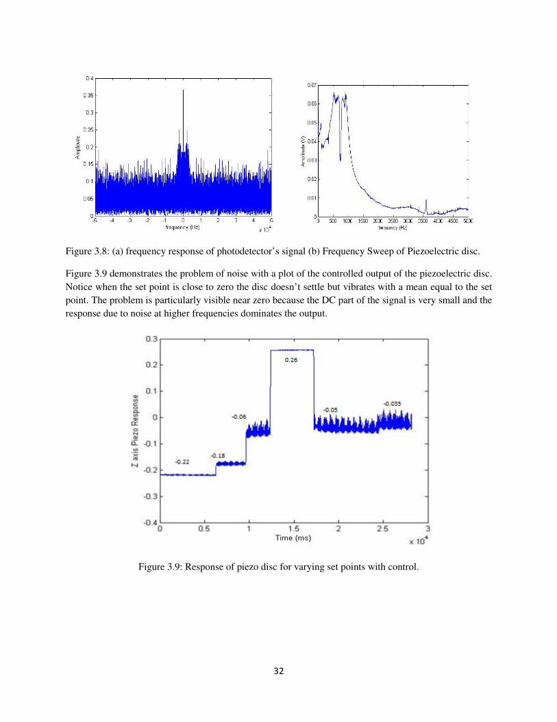
3.5.3 Sampling Rate, Bandwidth and Noise Considerations
Since the controller is designed on a noisy feedback loop, the bandwidth of the loop and the
clock frequency of the microcontroller become important. Figure 3.8 (a) shows a piece of y-axis
signal obtained at a sampling rate of 50 kHz. The frequency analysis of this signal reveals noise
components at higher frequencies. Note that the only useful data is present at DC (0 Hz). This is
problematic since the frequency sweep of the piezoelectric disc reveals that it has high amplitude
in the 600-1000 Hz range (figure 3.8 (b)). The Arduino Due board runs a typical PID controller
code at 200-400 KHz which creates enough bandwidth to allow noise in this range. The disc will
not settle at any point since a small component of photodetector’s noise is driving it at resonance.
This problem becomes clear when the code is executed. The piezo disc produces a sound due to
vibrations at resonance and is unable to settle at the given set point (figure 3.9).
32
Figure 3.8: (a) frequency response of photodetector’s signal (b) Frequency Sweep of Piezoelectric disc.
Figure 3.9 demonstrates the problem of noise with a plot of the controlled output of the piezoelectric disc.
Notice when the set point is close to zero the disc doesn’t settle but vibrates with a mean equal to the set
point. The problem is particularly visible near zero because the DC part of the signal is very small and the
response due to noise at higher frequencies dominates the output.
Figure 3.9: Response of piezo disc for varying set points with control.

33
Chapter 4
AFM Imaging
4.1 Acquiring Images
The AFM generates data that determines x and y axis displacement of the cantilever at the set
sampling rate of the data acquisition device. The data obtained this way is sequential and needs
to be sorted out. Some of the processing is done in real time while the scan is running and
remaining is done post-scan. Following are the steps taken to generate a raw AFM image
• Real time processing AFM data to remove noise and smoothen the signal
• Storing data for post-processing
• Sorting the sequential data into images
4.1.1 Noise Removal and Smoothening of signal
Before any enhancement can be made it is essential to find all the sources of noise present in the system
and their bandwidth so that they can be adequately filtered.
4.1.1.1 Sources of Noise in AFM
The noise in AFM data mainly comes from these sources:
• Shot noise: Most of the noise in the AFM data is shot noise of the Quadrant
Photodetector. This noise is due to randomness in the quantity of incoming photons in the
laser beam as well as randomness in generation of electrons in the semiconductor
material of the detector. This noise lies at high frequencies
• Johnson noise: This is a relatively small noise caused due to the trans-impedance
amplifiers in the Photodetector. Some of this noise comes from the X Y and Z axis
amplifiers and signal conditioning electronics.
• Mechanical vibrations: This part is negligible unless there is some activity in the
vicinity of the AFM. The apparatus is highly sensitive even to very small vibrations
including loud noises.
4.1.1.2 Noise Removal
Basic noise removal is done in real time by filtering the incoming data on the LabVIEW
interface. A moving average filter with a history of 20 samples is applied which acts as a low
pass filter and removes high frequency noise thus smoothening out the signal.

34
>?@A � BC∑ E?@ FAC�B
GHI ………. 4.1
This filter is enough to overcome the high frequency noise in the data and reveal true variations
in the signal. It is important to note that the sampling rate here is 1 KHz and the noise bandwidth
is 500 Hz (half of sampling frequency) for which a 20 sample moving average filter works well.
Figure 4.1: Photodetector signal (a) before filtering (b) after filtering.
4.1.2 Sorting Data into Images
After the signal is filtered, it is sorted into a Matrix. Matlab is used for this task. The sequential
vector containing the data is placed in successive rows of a matrix by correlating it with the fast
scan driving signal. Every other row is flipped since the cantilever moves back and forth while
scanning in the fast axis. After this the matrix is converted into a grayscale image with the
maximum value being assigned white color and the minimum being assigned black. So the raw
image shows the sample’s surface topography in the form of a grayscale. Features high in z axis
appear brighter than the lower ones. This image does not necessarily show a clear topography. In
fact small images of small features usually appear flat and featureless as the real information is
concealed within the large variations in data due to many image artifacts which are discussed
later in this chapter. To remove these unavoidable artifacts, image processing is necessary.
4.2 Processing AFM Images
Processing of any SPM data is done in these steps:
• Baseline correction and leveling
• Removing grains, scan strokes, abrupt maxima and minima (impulse noise)
• Image histogram specification and assigning color to data
• Frequency domain filtering (Smoothening, sharpening, mean, median etc.)

35
4.2.1 Baseline Correction
This is the most important and sometimes the only image processing step taken for the AFM
data. The motion of the piezoelectric discs is not linear and they move in a bowlike manner
which creates successive ups and downs in the image. These variations cover the entire color
scale and hide the surface topology. In addition, the sample and the optical bench are not
perfectly horizontal and a tilt of even few seconds of an arc creates rising and falling topology at
the nanometer scale. This is solved by fitting a curve to individual rows of the data. Typically a
first or second order polynomial is fitted and subtracted from the data. This corrects the baseline
of the image. The sample features become visible at this step.
Figure 4.2: Leveling AFM data to correct baseline. Image taken from [28]
4.2.2 Removing outliers, scan strokes and correcting scan lines
This is done by leveling outliers that appear in small patches usually in rectangles. This artifact is
caused due to the tip being dragged at some point in the scan. Other outliers and abrupt slopes
are also removed as they don’t represent any useful data. This step also removes artifacts in the
form of dark granular structures.
The AFM image rows sometimes get misaligned. This is removed by an algorithm that matches
height median over the image and corrects any such misalignment. All of this is done by a
specialized SPM analysis software called “Gwyddion”.

36
4.2.3 Image Histogram Specification
Usually the topography occupies a small part of the color range because of small variations in the
signal. This can be adjusted by specifying the maxima and minima of the data or by equalizing
the histogram of the image. Histogram Equalization assigns gray levels to images based on their
probability of occurrence in the image. So the topography is assigned a wider range of colors
which makes it clear for viewing. The image is also assigned a color scheme.
4.2.4 Frequency domain filtering
This step is optional and may not be needed. AFM images sometimes appear blurred or have
sudden variations or may contain noise. These images can be enhanced and cleaned with image
filters. A mean or median filter removes high frequency noise and impulse noise in the data. A
Laplacian filter sharpens the edges making the topology more crisp and clear. All these filters,
however, also have degrading effect on the image data. Smoothening the image may blur details
and sharpening the image will also enhance noise components in the image. So this step is
usually done by trial and error and multiple filters are applied to observe which function best.
Figure 4.2: Image filtering (a) original (b) median filtered (c) low pass filtered acquired on a silicon
sample with 500 nm SiO2 pillars.
4.3 Image Artifacts
4.3.1 Probe Artifacts
4.3.1.1 Blunt Probe
Typically, blunt probes will lead to images with features larger than expected, with a flattened
profile, due to the effect shown in figure 4.3. Note that holes in a flat surface will show the
opposite effect, appearing smaller with blunt probes than with sharp ones.

37
Figure 4.3: Effect of sharp and blunt probe.
4.3.1.2 Contaminated or Broken Probes
Contamination of AFM probes is quite common, and scanning certain samples leads to dirty
probes more quickly than others. In particular, biological or other soft samples, or any sample
with loose material at the surface, tending to contaminate probe tips quickly, and ultimately
leading to image degradation [30].
4.3.1.3 Probe Sample Angle
When scanning large features, artifacts can be introduced by having a large angle between the
probe and the sample, as illustrated in Figure 4.4. This problem is solved by adjusting the angle
between the probe and the sample so that they are perpendicular.
Figure 4.4 Angled probe
4.3.2 Piezoelectric Scanner Artifacts
4.3.2.1 Scanner Bow
The piezoelectric disc used as a scanner moves in a slightly curved motion making a bow
creating a false contour on the resulting images. This appears as slightly bright background at the
center and darker at the edges. This artifact cannot be removed in the hardware. It is removed by
correcting the baseline in the software as discussed in section 4.2.1.
38
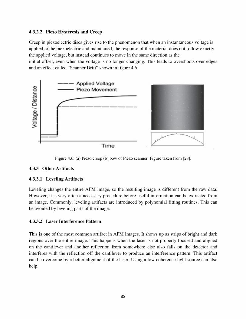
4.3.2.2 Piezo Hysteresis and Creep
Creep in piezoelectric discs gives rise to the phenomenon that when an instantaneous voltage is
applied to the piezoelectric and maintained, the response of the material does not follow exactly
the applied voltage, but instead continues to move in the same direction as the
initial offset, even when the voltage is no longer changing. This leads to overshoots over edges
and an effect called “Scanner Drift” shown in figure 4.6.
Figure 4.6: (a) Piezo creep (b) bow of Piezo scanner. Figure taken from [28].
4.3.3 Other Artifacts
4.3.3.1 Leveling Artifacts
Leveling changes the entire AFM image, so the resulting image is different from the raw data.
However, it is very often a necessary procedure before useful information can be extracted from
an image. Commonly, leveling artifacts are introduced by polynomial fitting routines. This can
be avoided by leveling parts of the image.
4.3.3.2 Laser Interference Pattern
This is one of the most common artifact in AFM images. It shows up as strips of bright and dark
regions over the entire image. This happens when the laser is not properly focused and aligned
on the cantilever and another reflection from somewhere else also falls on the detector and
interferes with the reflection off the cantilever to produce an interference pattern. This artifact
can be overcome by a better alignment of the laser. Using a low coherence light source can also
help.

39
Figure 4.7: Laser interference pattern visible in generated image.
4.3.3.3 Vibrations
Vibrations in the vicinity due to other machinery, sound or vibrations of the building can cause
periodic patterns in the image. This can be avoided by isolating the AFM apparatus from loud
noise and damping the table on which it is placed to cancel floor vibrations.
The AFM has been setup on an optical bench which dampens mechanical vibrations with springs
present inside screw holes. The optical assembly is covered from all sides to isolate from air
drafts, light and sound.
4.4 Actual Images
The very first image we scanned was of a calibration sample having 500 nm SiO2 pillars on a Si
substrate (figure 4.8). Figure 4.9 shows the results of the scan. The scanner was able to pick up
two pillars which can be seen in yellow color against brown background. This image, although
very clear has scratches in it specially near the border of the pillars. This indicates that the
contact was strong and the tip had dragged over the sample’s surface.

40
Figure 4.8: 500 nm calibration sample with scan region marked in blue (HS500MG
manufactured by Tedpella).
The image processing steps involved were
• Baseline correction: figure 4.9 (a) shows the slanted base of the scan which was corrected
to get correct features.
• Histogram equalization: more color range was provided to the pillars and the background.
This was necessary since there were patches of outliers (colored black) which were not
part of the topology and needed to be suppressed.
• Some scan strokes were removed using Gwyddion’s algorithms to make the image more
clear.

41
Figure 4.9: (a) Raw line scans, (b) Y axis image and (c) X axis image of a 500 nm calibration
sample.
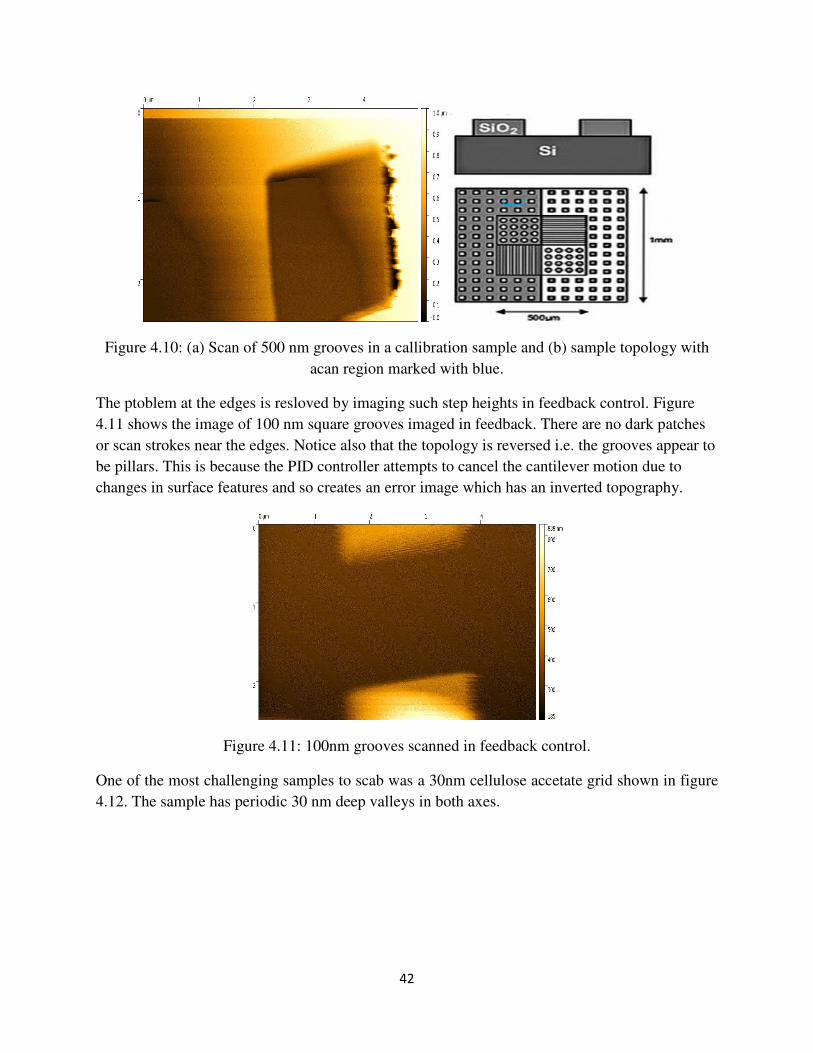
Features of smaller size were also scanned. Figure 4.10 shows scan of 500nm square grooves in a
sillicon substrate. A similar sequence of image processing steps as discussed for the previous
image were used. It is important to note that this image, like the other, has laack patches at the
edges of the groove. This happens when the laser goes off the detector’s surface when the
cantilever is climbing up a step because the tip bends in tip’s reflecting surface bends away from
the step as the tip climbs up. Notics that the boundary where the tip falls down does not have
such black patches.
42
Figure 4.10: (a) Scan of 500 nm grooves in a callibration sample and (b) sample topology with
acan region marked with blue.
The ptoblem at the edges is resloved by imaging such step heights in feedback control. Figure
4.11 shows the image of 100 nm square grooves imaged in feedback. There are no dark patches
or scan strokes near the edges. Notice also that the topology is reversed i.e. the grooves appear to
be pillars. This is because the PID controller attempts to cancel the cantilever motion due to
changes in surface features and so creates an error image which has an inverted topography.
Figure 4.11: 100nm grooves scanned in feedback control.
One of the most challenging samples to scab was a 30nm cellulose accetate grid shown in figure
4.12. The sample has periodic 30 nm deep valleys in both axes.

43
Figure 4.12: Topography of 30 nm cellulose accetate grid (model no: 607-AFM manufactored by
Tedpella).
Imaging this sample gives a unique opportnity to ellaborate on chalenges in AFM imaging that is
to extract a weak topographical signal masqueraded by artifacts. Consider figure 4.13:
• Initially the data is translated into a grayscale image and there is no feature visible. The
slanting baseline and a diagnally alligned bow is visible. These are scanner artifacts.
(figure 4.13 (a))
• Figure 4.13 (b) shows the image after subtracting a third order polynomial background
from the data. The uneven surface becomes flat
• Then the histogram is adjusted in such a way that maximum amount of color range is
given to the small variations that represent the actual topography. At this point a grid
pattern becomes visible as shown in figure 4.13 (c)
• Since the variations in topography are of the order of molecules, the cantilever can only
scan that part of the sample at which the force distance curve allows macimum variation
of force per unit change in distance. Sice the Piezo scanner is not linear as discussed in
section 2.2.3, this happens for a part of the image. That part is then cropped (figure 4.13
(d)) and further processed
• The final image is obtained after passing the image through frequency filters. I n the
present image (figure 4.13 (e)), a high pass filter has been applied with a window size
adjusted by hit-and-trial. For the current image the filter used a 5x5 laplacian window.

44
Figure 4.13: Steps in AFM image processing.
This sample is of high interest since it lies close of what the AFM is presently capable of
resolving. So this sample was imaged again with four times slower speed. The scan took 66
minutes and created a 2000x2000 pixel image. The result was significantly better than the
one in figure 4.13 (e). The grid lines are more clear especially in the direction of fast scan
that the previous image fails to clarify. Figure 4.14 shows this scan result.

45
Figure 4.14: 30 nm cellulose acetate grid scanned at a slower rate.
4.5 Further Improvements and Future Directions
4.5.1 Automated Tip Engagement
Commercial AFMs have an automatic process which engages the tip to the sample. This
construction requires a user to perform this task manually by observing the y axis signal of the
photodetector. Another addition would be augmenting the automatic engagement process to
adjusting level of contact of the tip. This will require the microcontroller to communicate with
the picomotor while the tip is being engaged to set the reference value.
4.5.2 Real Time Image enhancement and Processing
Most of the AFM image processing is done after the scan is done and the raw data is saved in
memory. A more robust way would be to have all the image processing steps to be done either in
real time while the scan is running or just after scan is complete by algorithms the require
minimal user inputs. An FPGA will be very suitable for this task due to its high clock speed and
ability to optimize digital algorithms to run at maximum speed.
4.5.3 Improved laser focusing and alignment
The laser spot is larger in size than the reflecting surface of the cantilever. Improvements can be
made by using lenses with much sharper focusing ability and expanding the laser beam before
focusing it.

46
4.5.4 MFM, EFM and the likes
This AFM project has set the base for any variant of SPM to be easily created by simply loading
the appropriate probe. All the data acquisition, processing and analysis tools have been designed
and interfaced with the hardware. This project will be able to provide scientists of
interdisciplinary interests to take measurements of many physical properties including friction
and surface properties, thermal properties, magnetic coefficients etc.

47
References
[1] Shmalz, G., Uber Glatte und Ebenheit als physikalisches und physiologishes Problem.Verein
Deutscher Ingenieure 1929, 1461–67.
[2] Becker, H.; Bender, O.; Bergmann, L.; Rost, K.; Zobel, A. Apparatus for measuring surface
irregularities. United States Patent number: 2728222, 1955.
[3] Young, R.; Ward, J.; Scire, F., The topografiner: an instrument for measuring surface
microtopography. Review of Scientific Instruments 1972, 43 (7), 999–1011.
[4] Binnig, G.; Rohrer, H., Scanning tunneling microscopy. Helvetica Physica Acta 1982, 55 (6),
726–35.
[5] M. Shusteff1, T. P. Burg1 and S. R. Manalis. Measuring Boltzmann’s constant with a low-cost
atomic force microscope: An undergraduate experiment. American Journal of Physics 2006, 74–
873.
[6] Mitik-Dineva, N.; Wang, J.; Truong, V. K.; Stoddart, P.; Malherbe, F.; Crawford, R. J.;
Ivanova, E. P., Escherichia coli, Pseudomonas aeruginosa, and Staphylococcus aureus
attachment patterns on glass surfaces with nanoscale roughness. Current Microbiology 2009, 58
(3), 268–73.
[7] Sugimoto, Y.; Pou, P.; Abe, M.; Jelinek, P.; Perez, R.; Morita, S.; Custance, O., Chemical
identification of individual surface atoms by atomic force microscopy. Nature2007, 446 (7131),
64–67.
[8] Stipp, S. L. S., C. M. Eggleston, and B. S. Nielsen. Calcite surface structure observed at
microtopographic and molecular scales with atomic force microscopy (AFM). Geochimica et
Cosmochimica Acta 58.14 (1994): 3023-3033.
[9] Gao, Guangtu, et al. Atomic-scale friction on diamond: a comparison of different sliding
directions on (001) and (111) surfaces using MD and AFM. Langmuir 23.10 (2007): 5394-5405.
[10] Giessibl, F. J., Advances in atomic force microscopy. Reviews of Modern Physics 2003, 75
(3), 949–83.
[11] Gan, Y., Atomic and subnanometer resolution in ambient conditions by atomic force
microscopy.Surface Science Reports2009, 64 (3), 99–121.
[12] Zhang, Q.; Archer, L. A., Interfacial friction of surfaces grafted with one- and two-
component self-assembled monolayers.Langmuir2005, 21 (12), 5405–13.

48
[13] Cyganik, P.; Budkowski, A.; Raczkowska, J.; Postawa, Z., AFM/LFM surface studies of a
ternary polymer blend cast on substrates covered by a self-assembled monolayer. Surface
Science2002, 507–10, 700–6.
[14] Salaita, K.; Amarnath, A.; Maspoch, D.; Higgins, T. B.; Mirkin, C. A., Spontaneous ‘phase
separation’ of patterned binary alkanethiol mixtures. Journal of the American Chemical
Society2005, 127 (32), 11283–87.
[15] Puntes, Victor F., et al. Collective behaviour in two-dimensional cobalt nanoparticle
assemblies observed by magnetic force microscopy. Nature materials 3.4 (2004): 263-268.
[16] Maye, M. M.; Luo, J.; Han, L.; Zhong, C. J., Probing Ph-tuned morphological changes in
coreshell nanoparticle assembly using atomic force microscopy.Nano Letters2001, 1 (10), 575–
79.
[17] Boyd, Robert D., Siva K. Pichaimuthu, and Alexandre Cuenat. "New approach to inter-
technique comparisons for nanoparticle size measurements; using atomic force microscopy,
nanoparticle tracking analysis and dynamic light scattering." Colloids and Surfaces A:
Physicochemical and Engineering Aspects 387.1 (2011): 35-42.
[18] Stomp, Romain, et al. Detection of single-electron charging in an individual InAs quantum
dot by noncontact atomic-force microscopy. Physical review letters 94.5 (2005): 056802.
[19] Falvo, M. R.; Clary, G. J.; Taylor, R. M.; Chi, V.; Brooks, F. P.; Washburn, S.; Superfine,
R., Bending and buckling of carbon nanotubes under large strain.Nature1997, 389 (6651), 582–
84.
[20] Ho-Yin, C.; Ning, X.; Jiangbo, Z.; Guangyong, L.A deterministic process for fabrication
and assembly of single carbon nanotube based devices, 5th IEEE Conference on Nanotechnology
2005; pp 713–16.
[21] Jaganathan, H.; Ivanisevic, A., Heterostructured DNA templates: a combined magnetic
force microscopy and circular dichroism study.Applied Physics Letters2008, 93 (26), 263104–3.
[22] Best, Robert B., et al. Mechanical unfolding of a titin Ig domain: structure of transition state
revealed by combining atomic force microscopy, protein engineering and molecular dynamics
simulations. Journal of molecular biology 330.4 (2003): 867-877.
[23] Lyubchenko, Yuri, et al. Atomic force microscopy of long DNA: imaging in air and under
water. Proceedings of the National Academy of Sciences 90.6 (1993): 2137-2140.
[24] Gaboriaud, F.; Dufre ˆne, Y. F., Atomic force microscopy of microbial cells: application to
nanomechanical properties, surface forces and molecular recognition forces. Colloids and
Surfaces B: Biointerfaces2007, 54 (1), 10–19.

49
[25] Alsteens, David, et al. High-resolution imaging of chemical and biological sites on living
cells using peak force tapping atomic force microscopy. Langmuir 28.49 (2012): 16738-16744.
[26] Settimi, Valeria, and Giuseppe Rega. Influence of a locally-tailored external feedback
control on the overall dynamics of an AFM model. International Journal of Non-Linear
Mechanics 80 (2016): 144-159.
[27] Semi-Automatic Tuning of PID Gains for Atomic Force Microscopes Daniel Y.
Abramovitch, Storrs Hoen, and Richard Workman. American Control Conference 2008. 0743-
1619
[28] Eaton, Peter and West, Paul. Atomic Force Microscopy 2010. Oxford University Press
[29] Giessibl, F. J.; Hembacher, S.; Bielefeldt, H.; Mannhart, J., Subatomic features on the
silicon (111)-(77) surface observed by atomic force microscopy. Science 2000, 289 (5478), 422–
25.
[30] Taatjes, D. J.; Quinn, A. S.; Lewis, M. R.; Bovill, E. G., Quality assessment of atomic force
microscopy probes by scanning electron microscopy: correlation of tip structure with rendered
images. Microscopy Research and Technique 1999, 44 (5), 312–26.
50
Appendices
Appendix A: Software support
A1 LabVIEW Connection Diagram and User Interface
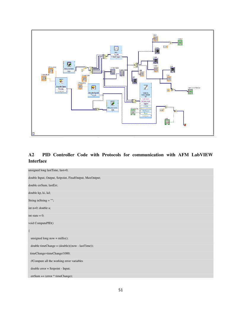
51
A2 PID Controller Code with Protocols for communication with AFM LabVIEW
Interface
unsigned long lastTime, last=0;
double Input, Output, Setpoint, FinalOutput, MaxOutput;
double errSum, lastErr;
double kp, ki, kd;
String inString = "";
int n=0; double a;
int state = 0;
void ComputePID()
{
unsigned long now = millis();
double timeChange = (double)((now - lastTime));
timeChange=timeChange/1000;
//Compute all the working error variables
double error = Setpoint - Input;
errSum += (error * timeChange);

52
double dErr = (error - lastErr) / timeChange;
//Compute PID Output
Output = kp * error + ki * errSum + kd * dErr;
if(Output>0)
{
if(Output>4095)
{
Output=4095;
}
FinalOutput=map(Output,0,4095,2048,4095);
}
else
{
if(Output<-4095)
{
Output=-4095;
}
FinalOutput=map(Output,-4095,0,0,2047);
}
//Remember some variables for next time
lastErr = error;
lastTime = now;
}
void SetSetpoint(double a)
{
Setpoint=a; //(a+0.25)*4095/0.5;
}
void SetTuning(double Kp, double Ki, double Kd)
{
kp = Kp;
ki = Ki;
kd = Kd;
}
void setup() {

53
Serial.begin(9600);
analogReadResolution(12);
analogWriteResolution(12);
SetTuning(0.025,0,0);
analogWrite(DAC1, 2047);
Input=analogRead(A5);
SetSetpoint(1800);
pinMode(33, OUTPUT);
}
void loop() {
//Serial communication
while (Serial.available() > 0)
{
char inChar = Serial.read();
if (inChar != '\n')
{
if(inChar == 'P') n=1;
else if(inChar == 'I') n=2;
else if(inChar == 'D') n=3;
else if(inChar == 'S') n=4;
else inString += (char)inChar;
}
else
{
a=inString.toFloat();
inString = "";
}
if(n==1) {kp=a;}
if(n==2) {ki=a;}
if(n==3) {kd=a;}
if(n==4) {SetSetpoint(a);}
SetTuning(kp,ki,kd);
}
Input=analogRead(A5);

54
ComputePID();
analogWrite(DAC1, FinalOutput);
Serial.print(Input);
Serial.print(',');
Serial.print(FinalOutput);
Serial.print(",");
Serial.println(Setpoint);
delay(1);
A3 Matlab Code for Image Generation
% X is the Y axis sequential data from Photodetector x=x'; img=x(1511:2510); n=613; while n<=998 n1=1000*(n-1)+711; n2=(1000*n)+710; img=[img;x(n1:n2)]; n=n+2; end img1=mat2gray(img); imshow(img1) imwrite(img1, 'AFMimage.jpg');

55
Appendix B: Hardware Support
B1 Electronics Connection Diagram
B2 PDQ80A Quadrant Photodetector Documentation

56
B3 New Focus Piezo Linear Actuator Picomotor

57
B4 Newport ULTRALign Precision XYZ Motion Stage