Embed Size (px)
Citation preview
JOURNAL OF SEMICONDUCTOR TECHNOLOGY AND SCIENCE, VOL.17, NO.2, APRIL, 2017 ISSN(Print) 1598-1657 https://doi.org/10.5573/JSTS.2017.17.2.210 ISSN(Online) 2233-4866
Manuscript received Aug. 24, 2016; accepted Nov. 1, 2016 Inter-university Semiconductor Research Center (ISRC) and Department of Electrical and Computer Engineering, Seoul National University, Seoul 151-744, Korea E-mail : [email protected]
Implementation of Neuromorphic System with Si-based Floating-body Synaptic Transistors
Jungjin Park, Hyungjin Kim, Min-Woo Kwon, Sungmin Hwang, Myung-Hyun Baek,
Jeong-Jun Lee, Taejin Jang, and Byung-Gook Park*
Abstract—We have developed the neuromorphic system that can work with the four-terminal Si-based synaptic devices and verified the operation of the system using simulation tool and printed-circuit-board (PCB). The symmetrical current mirrors connected to the n-channel and p-channel synaptic devices constitute the synaptic integration part to express the excitation and the inhibition mechanism of neurons, respectively. The number and the weight of the synaptic devices affect the amount of the current reproduced from the current mirror. The double-stage inverters controlling delay time and the NMOS with large threshold voltage (VT) constitute the action-potential generation part. The generated action-potential is transmitted to next neuron and simultaneously returned to the back gate of the synaptic device for changing its weight based on spike-timing-dependent-plasticity (STDP). Index Terms—Neuromorphic, neuron circuit, synaptic device, action-potential, spike-timing-dependent-plasticity (STDP)
I. INTRODUCTION
Since the conventional electronic system originated from Von Neumann’s architecture has faced with fundamental physical limit and revealed the weakness in
terms of cost and efficiency [1-4], we feel the need to introduce the new paradigm of information processing. As an alternative to the convent ional system, the neuromorphic system inspired by human neural network has been developed, recently. Reflecting the pros and cons of recent research and considering space and power consumption, we proposed the neuromorphic system trying to emulate the neuron’s mechanism with a small number of MOSFETs and introduced Si-based synaptic device implementing the formation of memory and the signal transmission of biological neurons. As we use 4-terminal Si-based synapses and connect them to the neuron circuit without additional switch or logic operation, the proposed neuromorphic system can autonomously emulate the neuron’s mechanism with minimum power.
II. EXPERIMENTAL RESULTS
We designed the neuromorphic system as shown in Fig. 1. The neuron circuit is constructed by a total of 12 MOSFETs and 3 capacitors, except for synaptic devices, and consists of synaptic integration part and action-potential generation part. The integration part integrates and transmits the signal from pre- to post-neurons. The integration part is also divided into excitation part and inhibition part. The excitation part generates the current in the direction of increasing the capacitor voltage and the inhibition part generates the current in the reverse direction to the excitation part. The output pulse of the generation part is fed back to the back gate of the synaptic device for changing its weight based on spike-timing-dependent-plasticity (STDP).

JOURNAL OF SEMICONDUCTOR TECHNOLOGY AND SCIENCE, VOL.17, NO.2, APRIL, 2017 211
We utilized the Si-based floating-body synaptic transistor (SFST) in Fig. 2 as synaptic device that has short-term and long-term memory [5, 6]. Once the n-channel SFST is appropriately biased (e.g., VG = VDS = 2 V, VBG = -2 V), excess holes are generated by impact ionization near top gate and increase the potential of body region to accelerate the impact ionization. This positive feedback process lowers the energy barrier between source and body and the threshold voltage of the SFST. At the point when the source-body junction is forward biased due to the excess holes, the impact ionization occurs near back channel and the generated hot holes start to enter floating gate as shown in Fig. 3. Then, the decrease of the VT becomes permanent and the above process corresponds to the short term to long-term transition of memory. Fig. 4 shows the transient tendency of the hole accumulation in the body from the impact-ionization near the drain and the hole injection into the
floating gate. In order to observe the motion of the holes dramatically, we applied bias voltages to the synaptic device such as VG = VDS = 2 V, VBG = -2 V and set the
Fig. 1. Neuromorphic System with 4-terminal Si-based synaptic devices.
Fig. 2. Si-based floating-body synaptic transistor (SFST).
Fig. 3. Short-term to long-term transition in SFST.
Fig. 4. Transient tendency of hole concentration in body and floating gate in SFST.
212 JUNGJIN PARK et al : IMPLEMENTATION OF NEUROMORPHIC SYSTEM WITH SI-BASED FLOATING-BODY SYNAPTIC …
pulse width and the interval to 0.2 μs and 1 μs, respectively. As shown in Fig. 4, the triggering point that the holes are explosively generated and injected into the floating gate appears when the 5th pulse is applied to the device and it means the short-term to long-term transition.
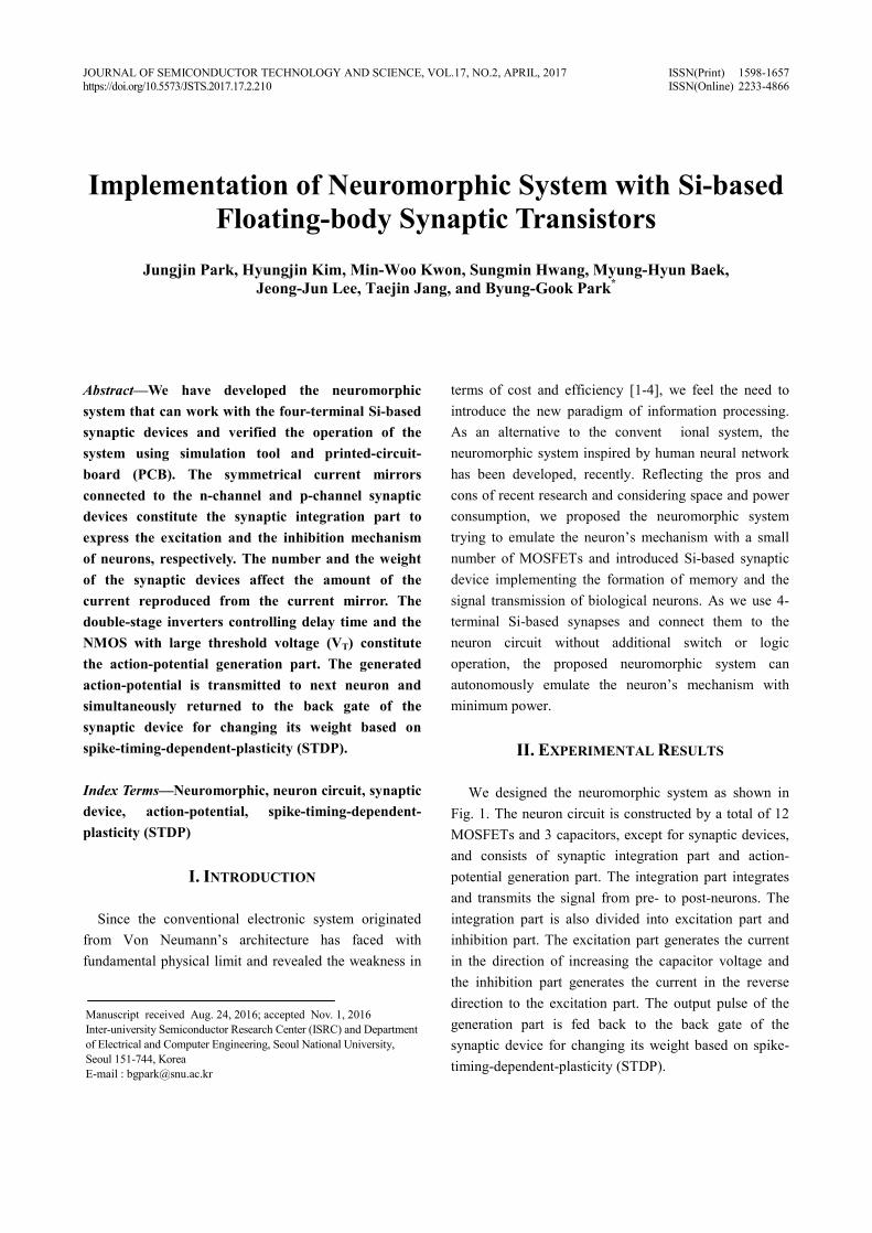
Fig. 5 shows the operation characteristics of the proposed system. The action-potential generation part in the proposed system creates an action-potential when the node voltage of capacitor C1 (VC1) exceeds threshold value. When the generation part turns on, the negative output of N5 appears first and the positive delayed output from double-stage inverters appears later to switch on N6. Finally, the N6 discharges the VC1 and the system returns to its initial state. Fig. 6 shows that the firing of the system depends on the number of the synaptic devices.
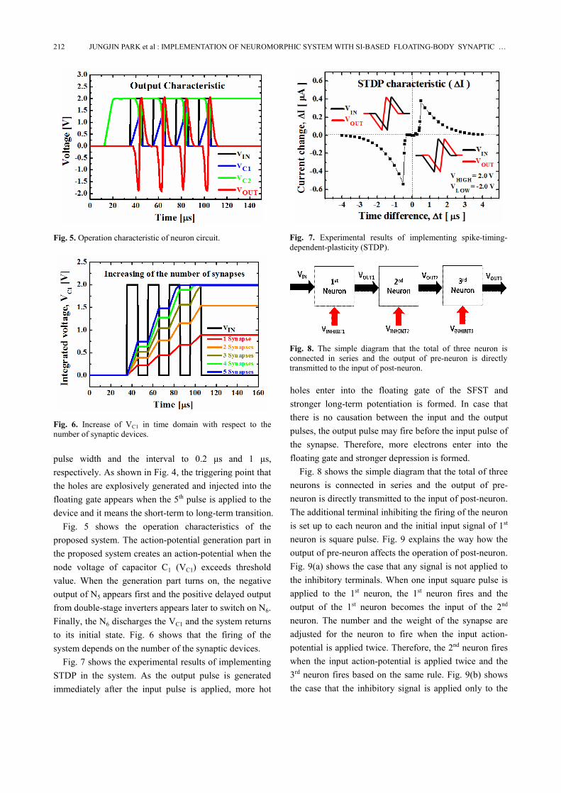
Fig. 7 shows the experimental results of implementing STDP in the system. As the output pulse is generated immediately after the input pulse is applied, more hot
holes enter into the floating gate of the SFST and stronger long-term potentiation is formed. In case that there is no causation between the input and the output pulses, the output pulse may fire before the input pulse of the synapse. Therefore, more electrons enter into the floating gate and stronger depression is formed.
Fig. 8 shows the simple diagram that the total of three neurons is connected in series and the output of pre-neuron is directly transmitted to the input of post-neuron. The additional terminal inhibiting the firing of the neuron is set up to each neuron and the initial input signal of 1st neuron is square pulse. Fig. 9 explains the way how the output of pre-neuron affects the operation of post-neuron. Fig. 9(a) shows the case that any signal is not applied to the inhibitory terminals. When one input square pulse is applied to the 1st neuron, the 1st neuron fires and the output of the 1st neuron becomes the input of the 2nd neuron. The number and the weight of the synapse are adjusted for the neuron to fire when the input action-potential is applied twice. Therefore, the 2nd neuron fires when the input action-potential is applied twice and the 3rd neuron fires based on the same rule. Fig. 9(b) shows the case that the inhibitory signal is applied only to the
Fig. 5. Operation characteristic of neuron circuit.
Fig. 6. Increase of VC1 in time domain with respect to the number of synaptic devices.
Fig. 7. Experimental results of implementing spike-timing-dependent-plasticity (STDP).
Fig. 8. The simple diagram that the total of three neuron is connected in series and the output of pre-neuron is directlytransmitted to the input of post-neuron.

JOURNAL OF SEMICONDUCTOR TECHNOLOGY AND SCIENCE, VOL.17, NO.2, APRIL, 2017 213
2nd neuron. Because the inhibited 2nd neuron can’t fire, the following neurons can’t fire. Similarly, when the inhibitory signal is applied only to the 1st or 3rd neuron, the following neurons can’t fire.
After verifying the operation of the neuron circuit and the synaptic device using simulation tool, we embodied the neuron circuit on printed-circuit-board (PCB). Fig. 10(a) shows the layout of neuron circuit for fabricating the PCB and Fig. 10(b) shows the scene for measuring the output characteristics of the fabricated PCB. We utilized a DC supply, pulse generator, oscilloscope for the measurement of the PCB. As we applied square pulse train having a size of 2.2 V and a width of 3 μs to a single neuron, the output characteristic such as Fig. 11(a) appears on the screen of oscilloscope. Similar to the simulation results, as the square pulse is applied, enough charge for the generation of action-potential is piled up to capacitor C1 and the action potential having intended
form is made. In case of Fig. 11(b), we connected two neuron circuits in series and the output pulse of the 1st circuit is directly applied to the input of the 2nd circuit. When the output pulse from the 1st neuron is applied twice to the input terminal of the 2nd neuron, the voltage of C1 passes over the threshold point of the 2nd neuron circuit and action potential is generated.
(a)
(b)
Fig. 9. Output characteristic of 3-Neurons connected in series (a) When any signal is not applied to the inhibitory terminal, all neurons can fire in succession, (b) When the inhibitory signal isapplied only to the 2nd neuron, the following neurons can’ fire.
(a) (b)
Fig. 10. (a) Layout of neuron circuit, (b) a scene for measurement of fabricated PCB.
(a)
(b)
Fig. 11. (a) Operation characteristic of single neuron circuit, (b) a pair of neuron circuit connected in series.

214 JUNGJIN PARK et al : IMPLEMENTATION OF NEUROMORPHIC SYSTEM WITH SI-BASED FLOATING-BODY SYNAPTIC …
III. CONCLUSIONS
We have developed neuromorphic system based on Si-based synaptic transistors, current mirrors and double-stage inverters. We verified the operation characteristic of the system using simulation tool and PCB. Without additional switch and logic operation, it successfully implemented the important functions of the signal transmission in human neural network such as potentiation, depression, excitation, inhibition, and STDP. Since we implemented the neural mechanism with simple analog operation and the minimum number of transistors, the proposed neuromorphic system has possibility to be applied efficiently to the various neuromorphic applications with minimum power and space.
ACKNOWLEDGMENTS
This work was supported by the Center for Integrated Smart Sensors funded by the Ministry of Science, ICT & Future Planning as Global Frontier Project (CISS-2012M3A6A6054186).
REFERENCES
[1] R. Ananthanarayanan et al., “The cat is out of the bag: Cortical simulations with 109 neurons, 1013 synapses”, in Proc. IEEE/ACM Conf. High Perform. Netw. Comput., 2009, pp. 1–12.
[2] S. Yu et al., “An electronic synapse device based on metal oxide resistive switching memory for neuromorphic computation”, IEEE Trans. Electron Devices, Vol. 58, No. 8, pp. 2729–2737, Aug., 2011.
[3] K. D. Cantley et al., “Hebbian learning in spiking neural networks with nanocrystalline Silicon TFTs and memristive synapses”, IEEE Trans. Nanotechnology, Vol. 10, No. 5, pp. 1066–1073, Sep., 2011.
[4] C. Zamarreño-Ramos et al., “On spike-timing-dependent-plasticity, memristive devices, and building a self-learning visual cortex”, Front. Neurosci, Vol. 5, Art. 16, Mar., 2011.
[5] H. Kim et al., “Silicon-based floating-body synaptic transistor,” Int. Conf. on Solid State Devices and Materials, pp. 322-323, Sep., 2012.
[6] H. Kim et al., “Silicon-Based floating-body synaptic transistor with frequency-dependent short-
and long-term memories,” IEEE Electron Device Letters, Vol. 37, No. 3, pp. 249-252, Mar., 2016.
[7] Y. Ota et al., “Analog implementation of pulse-coupled neural networks”, IEEE Trans. Neural Netw., Vol. 10, No. 3, pp. 539-544. May., 1999
[8] C. Lu et al., "Circuit design of an adjustable neuron activation function and its derivative," Electronics Letters, Vol. 36, No. 6, pp. 553-555, Mar., 2000.
[9] M. Boegerhausen et al., "Modeling short-term synaptic depression in silicon," Neural Comput., Vol. 15, No.2, pp. 331-348, Feb., 2003.
[10] T. Asai et al., "A subthreshold MOS neuron circuit based on the Volterra system," IEEE Trans. Neural Netw., Vol. 14, No. 5, pp. 1308-1312, Sep., 2003.
[11] G. Indiveri, E. Chicca, and R. Douglas, "A VLSI array of low-power spiking neurons and bistable synapses with spike-timing dependent plasticity," IEEE Trans. Neural Netw., Vol. 17, No.1, pp. 211-221, Jan., 2006.
[12] J. H. Wijekoon and P. Dudek, "Compact silicon neuron circuit with spiking and bursting behaviour," Neural Netw., Vol. 21, pp. 524-534, Mar., 2008.
[13] S. Ambrogio et al., "Spike-timing dependent plasticity in a transistor-selected resistive switching memory," Nanotechnology, Vol. 24, No. 38, pp. 384012-384020, Sep., 2013.
[14] S. Yu et al., "A neuromorphic visual system using RRAM synaptic devices with Sub-pJ energy and tolerance to variability: Experimental characterization and large-scale modeling, in IEDM Tech. Dig., 2012, pp. 239-242.
[15] S. Park et al., "RRAM-based synapse for neuromorphic system with pattern recognition function," in IEDM Tech. Dig., 2012, pp. 231-234.
[16] M.-W. Kwon et al., "Integrate-and-Fire neuron circuit and synaptic device using floating body MOSFET with spike timing- dependent plasticity," Journal of Semiconductor Technology and Science, Vol. 15, No. 6, pp. 658-663, Dec., 2015
Jungjin Park received the B.S. degree in 2010 from Seoul National University (SNU), Seoul, Korea, where he is currently working toward the Ph.D. degree in electrical and computer engineering. His research interests include synapse-like devices
and neuromorphic system.

JOURNAL OF SEMICONDUCTOR TECHNOLOGY AND SCIENCE, VOL.17, NO.2, APRIL, 2017 215
Min-Woo Kwon received the B.S. degree in 2012 from Seoul National University (SNU), Seoul, Korea, where he is currently working toward the Ph.D. degree in electrical and computer engineering. His research interests include nanoscale silicon
device and neuromorphic system.
Hyungjin Kim received the B.S. degree in 2010 and M.S. degree in 2012 from Seoul National University (SNU), Seoul, Korea, where he is currently working toward the Ph.D. degree in electrical and computer engineering. His research interests
include nanoscale silicon devices, tunnel field-effect transistor (TFET) and synapse-like devices.
Sungmin Hwang received the B.S. degree in 2014 from Hanyang University, Seoul, Korea, and he is currently working toward the Ph.D. degree in electrical and computer engineering from Seoul National University, Seoul, Korea. His
research interests include neuromorphic system.
Myung-Hyun Baek received the B.S. degree in 2013 from Seoul National University (SNU), Seoul, Korea, where he is currently working toward the Ph.D. degree in electrical and computer engineering. His research interests include synapse-like devices
and neuromorphic system.
Jeong-Jun Lee received the B.S. degree in 2016 from Seoul National University (SNU), Seoul, Korea, where he is currently working toward the M.S. degree in electrical and computer engineering. His research interests include synapse-like devices
and neuromorphic system.
Taejin Jang received the B.S. degree in 2016 from Seoul National University (SNU), Seoul, Korea, where he is currently working toward the M.S. degree in electrical and computer engineering. His research interests include synapse-like devices
and neuromorphic system.
Byung-Gook Park received his B.S. and M.S. degrees in electronics engineering from Seoul National University (SNU) in 1982 and 1984, respectively, and his Ph. D. degree in electrical engineering from Stanford University in 1990. From 1990 to
1993, he worked at the AT&T Bell Laboratories, where he contributed to the development of 0.1 micron CMOS and its characterization. From 1993 to 1994, he was with Texas Instruments, developing 0.25 micron CMOS. In 1994, he joined SNU as an assistant professor in the School of Electrical Engineering (SoEE), where he is currently a professor. In 2002, he worked at Stanford University as a visiting professor, on his sabbatical leave from SNU. He led the Inter-university Semiconductor Research Center (ISRC) at SNU as the director from 2008 to 2010. His current research interests include the design and fabrication of nanoscale CMOS, flash memories, silicon quantum devices and organic thin film transistors. He has authored and co-authored over 1000 research papers in journals and conferences. Prof. Park has served as a committee member on several international conferences including Microprocesses and Nanotechnology, IEEE International Electron Devices Meeting, International Conference on Solid State Devices and Materials, and IEEE Silicon Nanoelectronics Workshop and served as an Editor of IEEE Electron Device Letters. He received “Best Teacher” Award from SoEE in 1997, Doyeon Award for Creative Research from ISRC in 2003, Educational Award from College of Engineering, SNU, in 2006, Haedong Research Award from IEEK in 2008, Nano Research Innovation Award from the Ministry of Science, ICT and Future Planning of Korea in 2013, and Academic Training Award from Seoul National University in 2015.