Embed Size (px)
Citation preview

1
Implementing super-efficient FFTs in Altera
FPGAs Jérôme Leclère, Cyril Botteron, Pierre-André Farine
Electronics and Signal Processing Laboratory (ESPLAB), École Polytechnique Fédérale de Lausanne (EPFL),
Switzerland
E-mail : [email protected], [email protected]
How to cite this article : J. Leclère, C. Botteron, P.-A. Farine, “Implementing super-efficient FFTs in Altera
FPGAs", EE Times Programmable Logic Designline, February 2015. Available online at www.eetimes.com.
Abstract : In this article, an alternative method is proposed to compute a fast Fourier transform (FFT) on Altera
FPGAs. This method is using the Altera FFT intellectual property (IP) core, but it is more efficient than the
direct use of the Altera FFT IP core, in the sense that the processing time or the resources can be reduced. For
the FPGA user, the implementation of the proposed method is more complex than using directly the Altera FFT
IP core because additional elements are required, such as a numerically controlled oscillator (NCO) or a
memory, a complex multiplier, adders and scaling, but it may be worth it since the decrease in processing time or
resources is significant, especially regarding the memory with large FFTs. The proposed method can also be
applied to the computation of the convolution or correlation using FFTs.
1 Introduction
The fast Fourier transform (FFT) algorithms [1, 2] are widely used in many fields, whether for spectral analysis
to detect a signal, or for computation purposes (since for example the convolution of two signals can be
computed efficiently using FFTs, and the convolution is the operation performed by finite impulse response
filters) [3], or for compression purposes [4] or signal enhancements [5]. In other words, FFTs are everywhere.
Many applications requires the use of FPGAs, therefore, computing an FFT on an FPGA is an important
problem, even in domains such as astrophysics [6]. The FPGA companies usually provide an intellectual
property (IP) core to compute FFTs of length that is a power of two on their FPGA, such as Altera [7], Xilinx
[8], Lattice [9] or Microsemi [10]. One could think that such IP cores are optimized for the corresponding
FPGAs, however it has been found that a more efficient implementation of the Altera FFT is possible. More
efficient means that the resources can be reduced for a same processing time, or that the processing time can be
reduced for a moderate increase of the resources. The most surprising fact is that the alternative implementation
proposed here corresponds to one step of the well-known radix-2 FFT algorithm, where two FFTs of smaller
length are computed and the FFT inputs or outputs are combined.
In Section 2, we review the characteristics and parameters of the Altera FFT. In Section 3, we recall the radix-2
FFT algorithm, and show how it can be used to reduce the processing time or the resources with the Altera FFT.
In Section 4, the same idea is applied for the convolution computed by FFT. Section 5 provides an application
example, indicating the additional complications of the proposed implementation and the real resource usage.
Finally, Section 6 concludes this paper.
2 Description of the Altera FFT
The implementation of an FFT algorithm on an FPGA is not an easy task. Hopefully, FPGA companies usually
provide an FFT IP core. In this paper, we will concentrate on the FFT core provided by Altera, because we are
working with Altera FPGAs in our different research projects. The Altera FFT [7] is highly configurable, for
example we can select :
The transform length, which must be a power of two. Currently, the minimum length is 8 points and the
maximum length is 262 144 points (this is for the version 14.1 of August 2014; the maximum length
may grow in the next years).
The input/output (I/O) data flow (more details about this are provided below).

2
The number of bits to quantify the input data, the output data, and the twiddle factors.
The order of the input and of the output (natural order or bit-reversed order, see Chapter 2 of [11] for
more information on this).
Some options for the FFT engine.
Some options for the implementation of the complex multipliers (we can use 4 multipliers and 2 adders
or 3 multipliers and 5 adders, and we can implement them using digital signal processing (DSP) blocks
or logic cells).
The repartition of the memory between the different memory types.
Regarding the I/O data flow, four are available : variable streaming, streaming, buffered burst, burst. For the
variable streaming and the streaming I/O data flows, the input and output data flows can be continuous, without
any break between consecutive transforms. The corresponding timing diagram of an 𝑁-point FFT (shown in Fig.
1 (a)) is given in Fig. 1 (b). Between the last input sample and the first output sample of the FFT, there is a
latency, denoted 𝐿𝑁, which depends on the transform length. Therefore, in this case, the 𝑃th FFT result is fully
available after 𝑁 + 𝐿𝑁 + 𝑃𝑁 = (𝑃 + 1)𝑁 + 𝐿𝑁 clock cycles. For the burst I/O data flow, it is possible to load a
new input only when the output is completely unloaded. This means that the throughput is reduced compared to
the variable streaming and streaming implementations. The buffered burst data flow is between the two previous
cases. The flow cannot be continuous, but it is not required to wait for the complete unload of the output samples
before loading new input samples.
Of course, the higher is the throughput, the higher are the required resources. For example, an estimate of the
resources considering three I/O data flows is provided in Table 1. Playing with the engine options may lower the
resources (logic, memory and DSP) for the buffered burst and burst I/O data flows, in exchange of a reduced
throughput.
FFT𝑁
(a)
3
1 2 3
1 2
4
𝑁
𝐿𝑁
(b)
Fig. 1: (a) 𝑵-point Altera FFT, (b) corresponding timing diagram with the streaming I/O data flow (the number in the
boxes identifies the sequences).
Table 1: Resources estimated with the Altera FFT IP core for an FFT of 2048 points implemented on a Cyclone V
FPGA, considering 16 bits for the data and twiddle precision, and 2 FFT engines with quad output. (1)Defined as the
minimum number of cycles between the start of two consecutive sequences. (2)An M10K memory contains 10 Kibit =
10 240 bits, however, the number of bits is divided by 8 instead of 10 for the conversion here due to the 16 bits
resolution and the memory limitation (see Chapter 2 of [12]).
I/O data flow Inverse of the
throughput(1)
(cycle)
Logic usage
(logical element, LE)
Memory usage Multipliers usage
(DSP block) bit M10K(2)
Streaming 2048 5930 311 296 38 12
Buffered Burst 2304 6186 245 760 30 12
Burst 5485 5709 114 688 14 12

3
Due to the large number of possibilities for the FFT implementation, for the evaluation of the resources in the
following sections, we will consider a Cyclone V FPGA, the streaming I/O data flow, a data and twiddle
precision of 16 bits, complex multipliers implemented in DSP blocks using four real multipliers, and no logic
function implemented in memory.
Under these conditions, the resources according to the FFT length are given in Table 2. It can be observed that
doubling the FFT length doubles the processing time, increases slightly the logic (except for some cases),
roughly doubles the memory (except for lengths lower than 512 points), and the number of DSP blocks stays the
same (except between 1024 and 2048 where it doubles). Seeing this, and knowing that an FFT can be computed
as two FFTs of length halved (or using time multiplexing technique, only one FFT of length halved can be used),
one can imagine that these characteristics can be exploited to improve the efficiency of the implementation,
which is shown in the next section.
Table 2: Resources estimated with the Altera FFT IP core for an implementation on a Cyclone V FPGA, considering
the streaming I/O data flow and 16 bits for the data and twiddle precision.
3 Efficient FFT computation on Altera FPGAs
3.1 Radix-2 FFT algorithm
The discrete Fourier transform (DFT) of a sequence 𝑛 of 𝑁 points is defined as
with = 0, 1, … , 𝑁 − 1. The radix-2 FFT algorithm consists in separating the input or the output in even and
odd samples, and repeats the process until a certain limit [11]. Doing so once for the input, we have
still with = 0, 1, … , 𝑁 − 1. The two sums does not correspond to DFTs because the range for and is
different. The first half of 𝑘 is obtained from Eq. (2) for = 0, 1,… , 𝑁/2 − 1, and is
FFT length Inverse of the
throughput (cycle)
Logic usage
(LE)
Memory usage
(bit)
Multipliers usage
(DSP block)
64 64 3584 90 112 6
128 128 3170 90 112 6
256 256 3741 90 112 6
512 512 4135 90 112 6
1024 1024 4712 155 648 6
2048 2048 5930 311 296 12
4096 4096 6331 622 592 12
8192 8192 6080 1 245 184 12
16 384 16 384 6487 2 334 720 12
32 768 32 768 6230 4 513 492 12
65 536 65 536 6644 8 871 936 12
𝑘 = ∑ 𝑛𝑒−𝑗2𝜋𝑘𝑛𝑁
𝑁−1
𝑛=0
, (1)
𝑘 = ∑ 2𝑛𝑒−𝑗2𝜋𝑘(2𝑛)
𝑁
𝑁/2−1
𝑛=0
+ ∑ 2𝑛+1𝑒−𝑗2𝜋𝑘(2𝑛+1)
𝑁
𝑁/2−1
𝑛=0
= ∑ 2𝑛𝑒−𝑗2𝜋𝑘𝑛𝑁/2
𝑁/2−1
𝑛=0
+ 𝑒−𝑗2𝜋𝑘𝑁 ∑ 2𝑛+1𝑒
−𝑗2𝜋𝑘𝑛𝑁/2
𝑁/2−1
𝑛=0
,
(2)
𝑘 = ∑ 2𝑛𝑒−𝑗2𝜋𝑘𝑛𝑁/2
𝑁/2−1
𝑛=0
+ 𝑒−𝑗2𝜋𝑘𝑁 ∑ 2𝑛+1𝑒
−𝑗2𝜋𝑘𝑛𝑁/2
𝑁/2−1
𝑛=0
, (3)

4
with = 0, 1, … , 𝑁/2 − 1 (in fact the equation is the same, only the range of has changed). The two sums
correspond to the DFT of the sequences 2𝑛 and 2𝑛+1, respectively. The second half of 𝑘 is obtained from Eq.
(2) for = 𝑁/2, 𝑁/2 + 1,… , 𝑁 − 1, and can be expressed as
with = 0, 1, … , 𝑁/2 − 1. The two sums are the same as for Eq. (3), therefore an FFT of 𝑁 points can be
computed using two FFTs of 𝑁/2 points as shown in Fig. 2 (a). In the same way, by separating the output in
even and odd samples, we obtain
with = 0, 1, … , 𝑁/2 − 1, 𝑛 is the first half of the input sequence, and 𝑛+𝑁/2 is the second half. The two sums
correspond to the DFT of the sequences 𝑛 + 𝑛+𝑁/2 and ( 𝑛 − 𝑛+𝑁/2)𝑒−𝑗2𝜋𝑛
𝑁 , respectively. Therefore, an FFT
of 𝑁 points can also be computed using two FFTs of 𝑁/2 points as shown in Fig. 2 (b).
–
FFT𝑁/2
2
FFT𝑁/2
2 +1 +𝑁/2
𝑒‒ 2 /𝑁
(a)
–
+𝑁/2
𝑒‒ 2 /𝑁
FFT𝑁/2
FFT𝑁/2
2
2 +1
(b)
Fig. 2 : Computation of an 𝑵-point FFT using two 𝑵/𝟐-point FFTs, (a) where the input is separated by parity and the
output is separated by section, (b) where the input is separated by section and the output is separated by parity.
3.2 Application to reduce the processing time
The timing diagram corresponding to the implementation of Fig. 2(a) using Altera FFTs is depicted in Fig. 3,
where 𝐿𝑁/2 denotes the latency of the FFT when the transform length is 𝑁/2. In this case, the 𝑃th FFT result is
fully available after 𝑁/2 + 𝐿𝑁/2 + 𝑃𝑁/2 = (𝑃 + 1)𝑁/2 + 𝐿𝑁/2 clock cycles. Therefore, compared to the direct
implementation of an 𝑁-point FFT, the processing time is approximately halved (see Fig. 1 (b)). Note however
that this requires having access to even and odd samples of the input sequence simultaneously.
For the evaluation of the resources, we consider 𝑁 = 2048, the resources for the FFT are estimated with the
Altera IP core, and the simple elements (multiplier and adder) can be easily estimated (see e.g. the models given
in [13]). The complex exponential in Fig. 2 (a) can be generated either using a numerically controlled oscillator
(NCO), such as the NCO IP core provided by Altera [14], or using a memory. There are different generation
algorithms for the NCO IP core of Altera, and the most interesting in terms of resources is the multiplier-based
one, which requires some logic, two M10K memories and two DSP blocks.
𝑘+𝑁/2 = ∑ 2𝑛𝑒−𝑗2𝜋𝑘𝑛𝑁/2
𝑁/2−1
𝑛=0
− 𝑒−𝑗2𝜋𝑘𝑁 ∑ 2𝑛+1𝑒
−𝑗2𝜋𝑘𝑛𝑁/2
𝑁/2−1
𝑛=0
, (4)
2𝑘 = ∑ ( 𝑛 + 𝑛+𝑁/2)𝑒−𝑗2𝜋𝑘𝑛𝑁/2
𝑁/2−1
𝑛=0
,
2𝑘+1 = ∑ ( 𝑛 − 𝑛+𝑁/2)𝑒−𝑗2𝜋𝑛𝑁 𝑒
−𝑗2𝜋𝑘𝑛𝑁/2
𝑁/2−1
𝑛=0
,
(5)

5
1 2
1 2
3 4 5 6 7 8
3 4 5 6 7 8
71 2 3 4 5 6
1 2 3 4 5 76
2
2 +1
+𝑁/2
𝑁/2
𝐿𝑁/2
Fig. 3: Timing diagram of the implementation of Fig. 2(a) using Altera FFTs (the number in the boxes identifies the
sequences).
If a memory is used instead, only 512 samples of 16 bits must be stored, since we need to generate half the
period of a cosine and a sine, which can be obtained from only a quarter of the period of a sine wave by inverting
the value and reading the memory in both directions, as shown in Fig. 4. Thus, using a dual port memory would
require only one M10K, which is more interesting than using an NCO in this case, therefore this option is
considered for the following. Note however, that for longer FFT lengths, the NCO becomes more interesting
because it would not require more resources while the memory would need to store more samples.
0 511
–1
0
memory
address
value
(a)
Read from 0 to 511+
inversion
–1
1
0
Read from 511 to 0 Read from 0 to 511Read from 511 to 0
(b)
Fig. 4: (a) Portion of a sine wave stored in the memory, (b) cosine and sine waves generated by reading the memory.
The y-axis is not scaled in this illustration (e.g. using 16 bits the amplitude would be 32 767).
6
Table 3: Comparison of the resources for Fig. 2 (a) and Fig. 1 (a) using the Altera FFT with 𝑵 = 𝟐𝟎𝟒𝟖 (estimation
based on Altera IP cores and models of [13]).
The summary of this basic estimation of the resources is given in Table 3, where we consider little logic for the
addressing of the memory (2 buses of 8 bits). It can be seen that the implementation of Fig. 2 (a) requires more
resources than the implementation of Fig. 1 (a), especially regarding the logic usage while the memory usage is
almost the same. However, as shown previously, the processing time for Fig. 2 (a) is half the one for Fig. 1 (a).
Since the resources are increased by a factor less than two, the implementation of Fig. 2 (a) is more efficient than
the implementation of Fig. 1 (a).
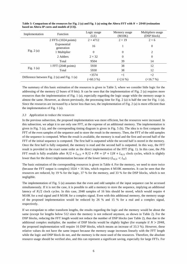
3.3 Application to reduce the resources
In the previous subsection, the proposed implementation was more efficient, but the resources were increased. In
this subsection, we adapt it to use only one FFT, at the expense of an additional memory. The implementation is
given in Fig. 5 (a), and the corresponding timing diagram is given in Fig. 5 (b). The idea is to first compute the
FFT of the even samples of the sequence and to store the result in the memory. Then, the FFT of the odd samples
of the sequence is computed. When the result is available, the memory is read and the first and second half of the
FFT of the initial sequence is computed. The first half is outputted while the second half is stored in the memory.
Once the first half is fully outputted, the memory is read and the second half is outputted. In this way, the FFT
result is provided in the exact same order as the direct implementation of the FFT (Fig. 1). In this case, the 𝑃th
FFT result is fully available after 𝑁/2 + 𝐿𝑁/2 +𝑁/2 + 𝑃𝑁 = (𝑃 + 1)𝑁 + 𝐿𝑁/2 clock cycles, which is slightly
lower than for the direct implementation because of the lower latency (𝐿𝑁/2 < 𝐿𝑁).
The basic estimation of the corresponding resources is given in Table 4. For the memory, we need to store twice
(because the FFT output is complex) 1024 × 16 bits, which requires 4 M10K memories. It can be seen that the
resources are reduced, by 19 % for the logic, 37 % for the memory, and 33 % for the DSP blocks, which is not
negligible.
The implementation of Fig. 5 (a) assumes that the even and odd samples of the input sequence can be accessed
simultaneously. If it is not the case, it is possible to add a memory to store the sequence, implying an additional
latency of 𝑁/2 clock cycles. In this case, 2048 samples of 16 bits should be stored, which would require 4
M10K for a real signal and 8 M10K for a complex signal. Even with this additional memory, the memory usage
of the proposed implementation would be reduced by 26 % and 15 % for a real and a complex signal,
respectively.
If we extrapolate to other transform lengths, the results regarding the logic and the memory would be about the
same (except for lengths below 512 since the memory is not reduced anymore, as shown in Table 2). For the
DSP blocks, reducing the FFT length would not reduce the number of DSP blocks (see Table 2), thus due to the
additional complex multiplier, the number of DSP blocks would be slightly higher (for example if 𝑁 > 2048,
the proposed implementation will require 16 DSP blocks, which means an increase of 33.3 %). However, these
relative values do not have the same impact because the memory usage increases linearly with the FFT length
while the logic and DSP block do not, and the memory is the most used of the resources. Therefore, the absolute
resource usage should be verified also, and this can represent a significant saving, especially for large FFTs. For
Implementation Function Logic usage
(LE)
Memory usage
(M10K)
Multipliers usage
(DSP block)
Fig. 2 (a)
2 FFTs (1024 points) 2 × 4712 2 × 19 2 × 6
Exponential
generation 16 1 0
1 Multiplier 0 0 2
2 Adders 2 × 32 0 0
Total 9504 39 14
Fig. 1 (a) 1 FFT (2048 points) 5930 38 12
Total 5930 38 12
Difference between Fig. 2 (a) and Fig. 1 (a) +3574 +1 +2
(+60.3 %) (+2.6 %) (+16.7 %)
7
example, if we now consider 𝑁 = 65 536, the estimation given in Table 5 shows that if the proposed
implementation has 4 additional DSP blocks (+33.3 %), the reduction of the memory resources (still of 37.1 %)
means that 402 M10K blocks are saved, which is a huge amount of resources. Even if we need to store the signal
before, this would require 256 M10K blocks for a complex signal (65 536 × 2 × 16 bits), meaning that there still
would be a saving of 146 M10K blocks.
–
Memory
𝑁,
,
FFT𝑁/2
𝑁,
𝑁, ,
,
,
𝑒‒ 2 /𝑁
2× 𝑁/2
(a)
2
0,
2 +1 2 2 +1 2 2 +1
1, 0, 1, 0, 1,
2 2 +1
0,
+𝑁/2 +𝑁/2
𝑁/2
𝐿𝑁/2
𝑁,
𝑁,
𝑁,
,
,
,
,
0, 0, 0, 0, +𝑁/2
0, +𝑁/2 0, +𝑁/2 0, +𝑁/2
+𝑁/2 +𝑁/2 +𝑁/2
+𝑁/2 +𝑁/2 +𝑁/2
(b)
Fig. 5: (a) Implementation of an 𝑵-point FFT using one 𝑵/𝟐-point FFT and a memory to reduce the resources, (b)
corresponding timing diagram using Altera FFTs (the colors inside the boxes identify the sequences).

8
Table 4: Comparison of the resources for Fig. 5 (a) and Fig. 1 (a) using the Altera FFT with 𝑵 = 𝟐𝟎𝟒𝟖 (estimation
based on Altera IP cores and models of [13]).
Table 5: Comparison of the resources for Fig. 5 (a) and Fig. 1 (a) using the Altera FFT with 𝑵 = 𝟔𝟓 𝟓𝟑𝟔 (estimation
based on Altera IP cores and models of [13]).
4 Efficient convolution computation on Altera FPGAs
4.1 Direct implementation of the convolution
The circular convolution of two sequences ℎ𝑛 and 𝑛 of 𝑁 points is defined as
with = 0, 1, … , 𝑁 − 1, and where mod denotes the modulo operation, i.e. ( + 𝑚𝑁) mod 𝑁 = with 𝑚 an
integer. The circular convolution can also be expressed as
where 𝑌𝑘, 𝐻𝑘 and 𝑘 are the DFTs of 𝑦𝑛, ℎ𝑛 and 𝑛, respectively. So, by computing the IDFT of 𝐻𝑘 𝑘 we obtain
𝑦𝑛. Therefore, the circular convolution can be computed efficiently as shown in Fig. 6 (a), and the corresponding
timing diagram is given in Fig. 6 (b). In this case, the 𝑃th convolution result is fully available after 𝑁 + 𝐿𝑁 +
𝑁 + 𝐿𝑁 + 𝑃𝑁 = (𝑃 + 2)𝑁 + 2𝐿𝑁 clock cycles.
Implementation Function Logic usage
(LE)
Memory usage
(M10K)
Multipliers usage
(DSP block)
Fig. 5 (a)
1 FFT (1024 points) 4712 19 6
Exponential
generation 16 1 0
1 Multiplier 0 0 2
2 Adders 2 × 32 0 0
1 Memory 22 4 0
Total 4814 24 8
Fig. 1 (a) 1 FFT (2048 points) 5930 38 12
Total 5930 38 12
Difference between Fig. 5 (a) and Fig. 1 (a) –1116 –14 –4
(–18.8 %) (–36.8 %) (–33.3 %)
Implementation Function Logic usage
(LE)
Memory usage
(M10K)
Multipliers usage
(DSP block)
Fig. 5 (a)
1 FFT (32 768 points) 6230 551 12
NCO exponential
generation 96 2 2
1 Multiplier 0 0 2
2 Adders 2 × 32 0 0
1 Memory 32 128 0
Total 6422 681 16
Fig. 1 (a) 1 FFT (65 536 points) 6644 1083 12
Total 6644 1083 12
Difference between Fig. 5 (a) and Fig. 1 (a) –222 –402 +4
(–3.3 %) (–37.1 %) (+33.3 %)
𝑦𝑛 = ∑ ℎ𝑘 (𝑛−𝑘) mod 𝑁
𝑁−1
𝑘=0
, (6)
𝑌𝑘 = 𝐻𝑘 𝑘, (7)

9
FFT𝑁
FFT𝑁
h 𝐻
IFFT𝑁
𝑌 𝑦
(a)
2
3
3
1
1
2 3 4
2 3 4
31 2
1 2
1 2
1
h
𝐻
𝑌
𝑦
𝑁
𝐿𝑁 𝐿𝑁
(b)
Fig. 6: (a) Implementation of the circular convolution of two sequences of 𝑵 points using FFTs, (b) corresponding
timing diagram using Altera FFTs (the colors inside the boxes identify the sequences).
4.2 Application of the radix-2 FFT
Replacing each FFT block in Fig. 6 (a) by the Fig. 2 (b), the circular convolution can be computed as shown in
Fig. 7 (a), and the corresponding timing diagram is given in Fig. 7 (b). In this case, the 𝑃th convolution result is
fully available after 𝑁/2 + 𝐿𝑁/2 +𝑁/2 + 𝐿𝑁/2 + 𝑃𝑁/2 = (𝑃 + 2)𝑁/2 + 2𝐿𝑁/2 clock cycles. Therefore,
compared to the direct implementation of the circular convolution (Fig. 6 (a)), the processing time is
approximately halved (see Fig. 6 (b)).
For the evaluation of the resources, the same conditions as in Section 3 are considered. The basic estimation of
the corresponding resources is given in Table 6. As in Section 3.2, the resources for the proposed
implementation are increased by a factor less than two while the processing time is halved. Therefore, the
implementation of Fig. 7 (a) is more efficient than the implementation of Fig. 6 (a). Note that moreover, slightly
different implementations than Fig. 7 (a), using four multipliers instead of five, are also possible (see Chapter 4
of [15]).
The same principle can be applied to reduce the resources of the convolution, by using three 𝑁/2-point FFTs
and an additional memory, and it can be verified that for the same processing time, the resources can be reduced
(the reduction is even slightly higher than for the computation of an FFT shown in Section 0, see Chapter 4 of
[15]).

10
–
–
–
+𝑁/2
h
h +𝑁/2
0,
1,
h1,
h0,
𝑒‒ 2 /𝑁
𝑒‒ 2 /𝑁
𝑒 2 /𝑁
FFT𝑁/2
FFT𝑁/2
FFT𝑁/2
FFT𝑁/2
IFFT𝑁/2
IFFT𝑁/2
𝑦1,
𝑦0, 𝑦
𝑦 +𝑁/2
(a)
6
1 2
1 2
3 4 5 6 7 8
3 4 5 6 7 8
71 2 3 4 5 6
1 2 3 4 5 76
71 2 3 4 5 6
1 2 3 4 5
,
h ,
𝐻 ,
,
𝑌 ,
𝑦 ,
𝑁/2
𝐿𝑁/2 𝐿𝑁/2 ∈ {0,1}
(b)
Fig. 7: (a) Implementation of a circular convolution of 𝑵 points using 𝑵/𝟐-point FFTs, where the inputs and the
output are separated by section, (b) corresponding timing diagram using Altera FFTs (the colors inside the boxes
identify the sequences).
11
Table 6: Comparison of the resources for Fig. 7 (a) and Fig. 6 (a) using the Altera FFT with 𝑵 = 𝟐𝟎𝟒𝟖 (estimation
based on Altera IP cores and models of [13]).
5 Application example
In the previous sections, the estimation of the resources was based on estimates from the Altera IP cores and
from models. To validate the previous results, the direct implementation of the Altera FFT (Fig. 1 (a)) and the
proposed implementation of the Altera FFT (Fig. 2 (a)) have been implemented into a Cyclone V FPGA, in order
to measure the resources after the place and route operation using the Quartus II software. The two
implementations (in fact three because the proposed one has been implemented with an NCO and with a memory
for the complex exponential generation), and validation by ModelSim and Matlab are available at
https://documents.epfl.ch/groups/e/es/esplab-unit/www/AlteraFFT/.
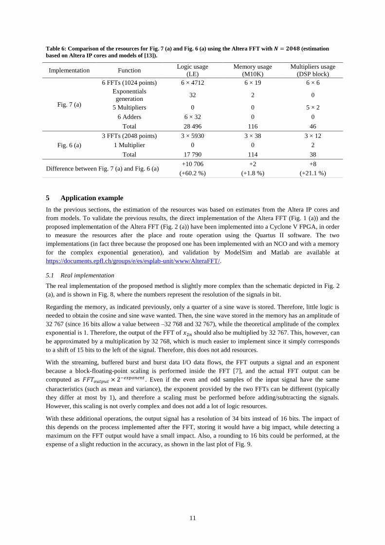
5.1 Real implementation
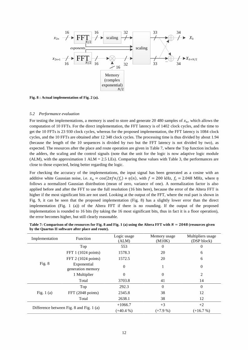
The real implementation of the proposed method is slightly more complex than the schematic depicted in Fig. 2
(a), and is shown in Fig. 8, where the numbers represent the resolution of the signals in bit.
Regarding the memory, as indicated previously, only a quarter of a sine wave is stored. Therefore, little logic is
needed to obtain the cosine and sine wave wanted. Then, the sine wave stored in the memory has an amplitude of
32 767 (since 16 bits allow a value between –32 768 and 32 767), while the theoretical amplitude of the complex
exponential is 1. Therefore, the output of the FFT of 2𝑛 should also be multiplied by 32 767. This, however, can
be approximated by a multiplication by 32 768, which is much easier to implement since it simply corresponds
to a shift of 15 bits to the left of the signal. Therefore, this does not add resources.
With the streaming, buffered burst and burst data I/O data flows, the FFT outputs a signal and an exponent
because a block-floating-point scaling is performed inside the FFT [7], and the actual FFT output can be
computed as 𝐹𝐹 𝑜𝑢𝑡𝑝𝑢𝑡 × 2−𝑒𝑥𝑝𝑜𝑛𝑒𝑛𝑡 . Even if the even and odd samples of the input signal have the same
characteristics (such as mean and variance), the exponent provided by the two FFTs can be different (typically
they differ at most by 1), and therefore a scaling must be performed before adding/subtracting the signals.
However, this scaling is not overly complex and does not add a lot of logic resources.
With these additional operations, the output signal has a resolution of 34 bits instead of 16 bits. The impact of
this depends on the process implemented after the FFT, storing it would have a big impact, while detecting a
maximum on the FFT output would have a small impact. Also, a rounding to 16 bits could be performed, at the
expense of a slight reduction in the accuracy, as shown in the last plot of Fig. 9.
Implementation Function Logic usage
(LE)
Memory usage
(M10K)
Multipliers usage
(DSP block)
Fig. 7 (a)
6 FFTs (1024 points) 6 × 4712 6 × 19 6 × 6
Exponentials
generation 32 2 0
5 Multipliers 0 0 5 × 2
6 Adders 6 × 32 0 0
Total 28 496 116 46
Fig. 6 (a)
3 FFTs (2048 points) 3 × 5930 3 × 38 3 × 12
1 Multiplier 0 0 2
Total 17 790 114 38
Difference between Fig. 7 (a) and Fig. 6 (a) +10 706 +2 +8
(+60.2 %) (+1.8 %) (+21.1 %)
12
–16
16
16
16
32
32
16
Memory
(complex
exponential)
scaling
33
33
34
34
scalingexponents
FFT𝑁/2
FFT𝑁/2
2
2 +1
+𝑁/2
𝑁/2
Fig. 8 : Actual implementation of Fig. 2 (a).
5.2 Performance evaluation
For testing the implementations, a memory is used to store and generate 20 480 samples of 𝑛, which allows the
computation of 10 FFTs. For the direct implementation, the FFT latency is of 1402 clock cycles, and the time to
get the 10 FFTs is 23 930 clock cycles, whereas for the proposed implementation, the FFT latency is 1084 clock
cycles, and the 10 FFTs are obtained after 12 348 clock cycles. The processing time is thus divided by about 1.94
(because the length of the 10 sequences is divided by two but the FFT latency is not divided by two), as
expected. The resources after the place and route operation are given in Table 7, where the Top function includes
the adders, the scaling and the control signals (note that the unit for the logic is now adaptive logic module
(ALM), with the approximation 1 ALM = 2.5 LEs). Comparing these values with Table 3, the performances are
close to those expected, being better regarding the logic.
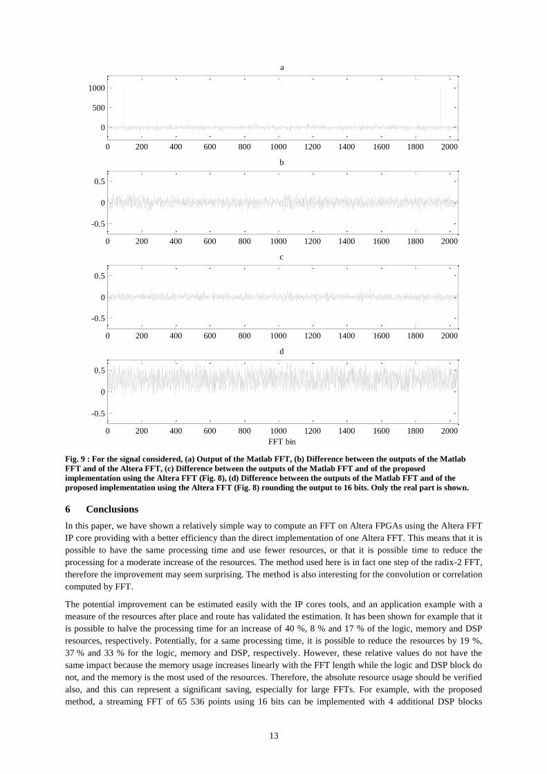
For checking the accuracy of the implementations, the input signal has been generated as a cosine with an
additive white Gaussian noise, i.e. 𝑛 = cos(2 𝑓 /𝑓𝑠) + 𝜂( ), with 𝑓 = 200 kHz, 𝑓𝑠 = 2.048 MHz, where 𝜂
follows a normalized Gaussian distribution (mean of zero, variance of one). A normalization factor is also
applied before and after the FFT to use the full resolution (16 bits here), because the error of the Altera FFT is
higher if the most significant bits are not used. Looking at the output of the FFT, where the real part is shown in
Fig. 9, it can be seen that the proposed implementation (Fig. 8) has a slightly lower error than the direct
implementation (Fig. 1 (a)) of the Altera FFT if there is no rounding. If the output of the proposed
implementation is rounded to 16 bits (by taking the 16 most significant bits, thus in fact it is a floor operation),
the error becomes higher, but still clearly reasonable.
Table 7: Comparison of the resources for Fig. 8 and Fig. 1 (a) using the Altera FFT with 𝑵 = 𝟐𝟎𝟒𝟖 (resources given
by the Quartus II software after place and route).
Implementation Function Logic usage
(ALM)
Memory usage
(M10K)
Multipliers usage
(DSP block)
Fig. 8
Top 553 0 0
FFT 1 (1024 points) 1578.3 20 6
FFT 2 (1024 points) 1572.5 20 6
Exponential
generation memory 0 1 0
1 Multiplier 0 0 2
Total 3703.8 41 14
Fig. 1 (a)
Top 292.3 0 0
FFT (2048 points) 2345.8 38 12
Total 2638.1 38 12
Difference between Fig. 8 and Fig. 1 (a) +1066.7 +3 +2
(+40.4 %) (+7.9 %) (+16.7 %)
13
Fig. 9 : For the signal considered, (a) Output of the Matlab FFT, (b) Difference between the outputs of the Matlab
FFT and of the Altera FFT, (c) Difference between the outputs of the Matlab FFT and of the proposed
implementation using the Altera FFT (Fig. 8), (d) Difference between the outputs of the Matlab FFT and of the
proposed implementation using the Altera FFT (Fig. 8) rounding the output to 16 bits. Only the real part is shown.
6 Conclusions
In this paper, we have shown a relatively simple way to compute an FFT on Altera FPGAs using the Altera FFT
IP core providing with a better efficiency than the direct implementation of one Altera FFT. This means that it is
possible to have the same processing time and use fewer resources, or that it is possible time to reduce the
processing for a moderate increase of the resources. The method used here is in fact one step of the radix-2 FFT,
therefore the improvement may seem surprising. The method is also interesting for the convolution or correlation
computed by FFT.
The potential improvement can be estimated easily with the IP cores tools, and an application example with a
measure of the resources after place and route has validated the estimation. It has been shown for example that it
is possible to halve the processing time for an increase of 40 %, 8 % and 17 % of the logic, memory and DSP
resources, respectively. Potentially, for a same processing time, it is possible to reduce the resources by 19 %,
37 % and 33 % for the logic, memory and DSP, respectively. However, these relative values do not have the
same impact because the memory usage increases linearly with the FFT length while the logic and DSP block do
not, and the memory is the most used of the resources. Therefore, the absolute resource usage should be verified
also, and this can represent a significant saving, especially for large FFTs. For example, with the proposed
method, a streaming FFT of 65 536 points using 16 bits can be implemented with 4 additional DSP blocks
0 200 400 600 800 1000 1200 1400 1600 1800 2000
0
500
1000
a
0 200 400 600 800 1000 1200 1400 1600 1800 2000
-0.5
0
0.5
b
0 200 400 600 800 1000 1200 1400 1600 1800 2000
-0.5
0
0.5
c
0 200 400 600 800 1000 1200 1400 1600 1800 2000
-0.5
0
0.5
FFT bin
d

14
(+33 %) but with about 400 M10K blocks less (–37 %), for the same processing time, which is clearly
interesting because this represents a huge amount of resources. Finally, the actual improvement will depend on
the I/O data flow, the parameters and the FPGA selected.
7 References
1 L. Brigham, “The fast Fourier transform and its applications”, Prentice Hall, 1988.
2 P. Duhamel, M. Vetterli, “Fast Fourier transforms: A tutorial review and a state of the art”, Signal
Processing, vol. 19, no. 4, pp 259–299, 1990.
3 H.J. Nussbaumer, “Fast Fourier transform and convolution algorithms”, Springer, 2nd edition, 1982.
4 S.W. Smith, “Digital signal processing: a practical guide for engineers and scientists”, Newnes, 2002.
5 A.E. Zonst, “Understanding FFT applications”, Citrus Press, 2nd edition, 2003.
6 T.S. Czajkowski, C.J. Comis, M. Kawokgy, “Fast Fourier transform implementation for high speed
astrophysics applications on FPGAs”, VLSI Systems Project Report, June 2004.
7 Altera, “FFT MegaCore Function – User Guide”, August 2014.
8 Xilinx, “LogiCORE IP Fast Fourier Transform – Product Guide”, April 2014.
9 Lattice, “FFT Compiler IP Core User’s Guide”, August 2011.
10 Microsemi, “Core FFT – Handbook”, September 2013.
11 R.G. Lyons, “Understanding digital signal processing”, Prentice Hall, 4th edition, 2010.
12 Altera, “Cyclone V Device Handbook, Volume 1”, July 2014.
13 J. Leclère, C. Botteron, P.-A. Farine, “Comparison Framework of FPGA-Based GNSS Signals Acquisition
Architectures”, IEEE Transactions on Aerospace and Electronic Systems, vol. 49, no. 3, pp 1497–1518,
2013.
14 Altera, “NCO MegaCore Function – User Guide”, August 2014.
15 J. Leclère, “Resource-efficient parallel acquisition architectures for modernized GNSS signals”, PhD
thesis, EPFL, 2014.
Author biographies
Dr. Jérôme Leclère received a master and an engineering degree in Electronics and Signal Processing from
ENSEEIHT, Toulouse, France, in 2008, and his Ph.D. in the GNSS field from EPFL, Switzerland, in 2014. He
focused his researches in the reduction of the complexity of the acquisition of GNSS signals, with application to
hardware receivers, especially using FPGAs. He developed an FPGA-based high sensitivity assisted GPS L1
C/A receiver, and participated to the design of several FPGA receivers, for space applications (L1 C/A) and for
GNSS reflectometry (L1/E1).
Dr. Cyril Botteron is leading, managing, and coaching the research and project activities of the Global
Navigation Satellite System and Ultra-Wideband and mm-wave groups at École Polytechnique Fédérale de
Lausanne (EPFL). He is the author or co-author of 5 patents and over 100 publications in major journals and
conferences in the fields of wireless positioning systems, GNSS-based navigation and sensing, ultra-low-power
radio frequency communications and integrated circuits design, and baseband analog and digital signal
processing.
Prof. Pierre-André Farine is professor in electronics and signal processing at EPFL, and is head of the electronics
and signal processing laboratory. He received the M.Sc. and Ph.D. degrees in Micro technology from the
University of Neuchâtel, Switzerland, in 1978 and 1984, respectively. He is active in the study and
implementation of low-power solutions for applications covering wireless telecommunications, ultra-wideband,
global navigation satellite systems, and video and audio processing. He is the author or co-author of more than
120 publications in conference and technical journals and 50 patent families (more than 270 patents).