Embed Size (px)
Citation preview
Importance of Materials Processing
All electronic devices & systems are made of materials in
various combinations
Raw materials are far from the final electronic products
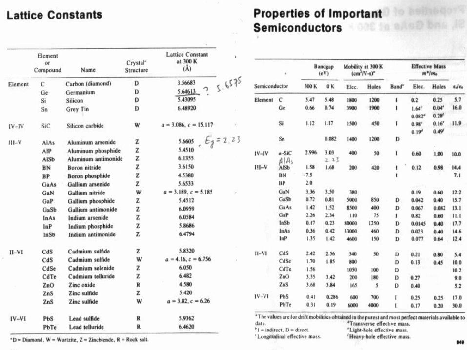
Semiconductor materials (e.g., Si, Ge, GaAs, GaN...) used for
devices must be of extremely high purity and crystalline order
Real Materials and their Processing
Particles, lines and rigid bodies vs. real materials
Material-specific properties determine the function
and processing details of a material
Comprehensive knowledge of materials processing
requires ~ 5-10 years of learning and practice
Advantage and role of physics students
Different Types of Electronic Devices
Discrete devices: diodes, transistors, rectifiers, sensors, …
Integrated circuits (IC): CPU, DRAM, ASIC, …
Opto-electronics: LED, semiconductor laser (in CD/VCD players, optical communication), display, lighting, …
Solar cells: on satellites, calculators, large-scale power generation
Data storage: DRAM, hard disk, ZIP, flush memory, CD-ROM, ...
Electro-mechanic devices: electro-magnetic, piezo-electric, ...
Different Electronic Materials Semiconductors: Elemental (Si, Ge) & Compound (GaAs, GaN,
ZnS, CdS, …)
Insulators: SiO2, Al2O3, Si3N4, SiOxNy, ...
Conductors: Al, Au, Cu, W, silicides (metal-Si compounds), ...
Organic and polymer: liquid crystal, insulator, semiconductor, conductor
Composite materials: multi-layer structures, nano-materials, photonic crystals, ...
More: magnetic, superconductor, bio-material, …
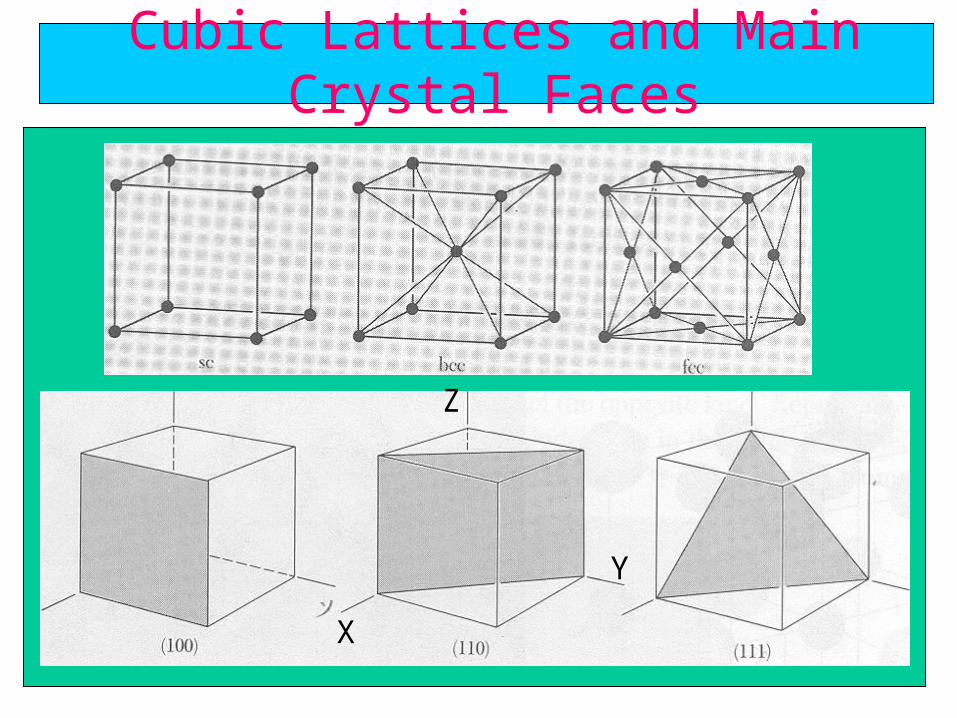
Cubic Lattices and Main Crystal Faces
X
Z
Y
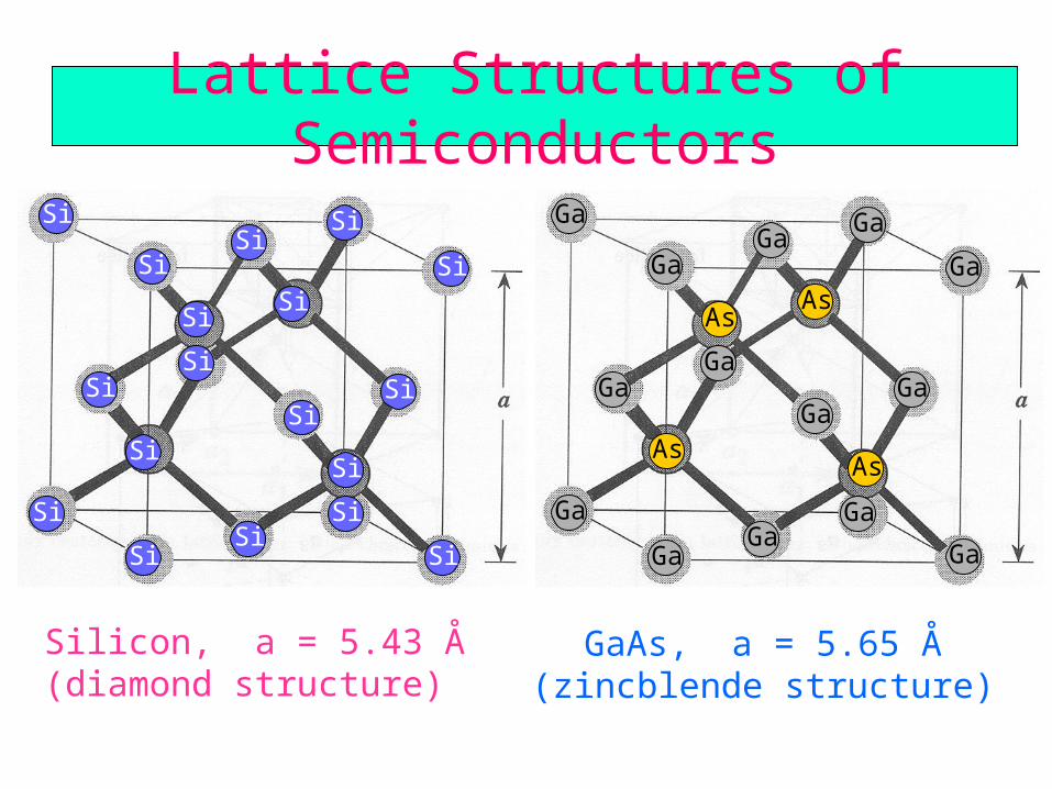
Lattice Structures of Semiconductors
Ga
Ga
Ga
Ga
GaGa
Ga
GaGa
Ga
Ga GaGa
Ga
AsAs
AsAs
Si
Si
Si
SiSi
Si
Si
Si
Si
Si
Si
Si
Si
SiSi
SiSi
Si
Silicon, a = 5.43 Å(diamond structure)
GaAs, a = 5.65 Å(zincblende structure)
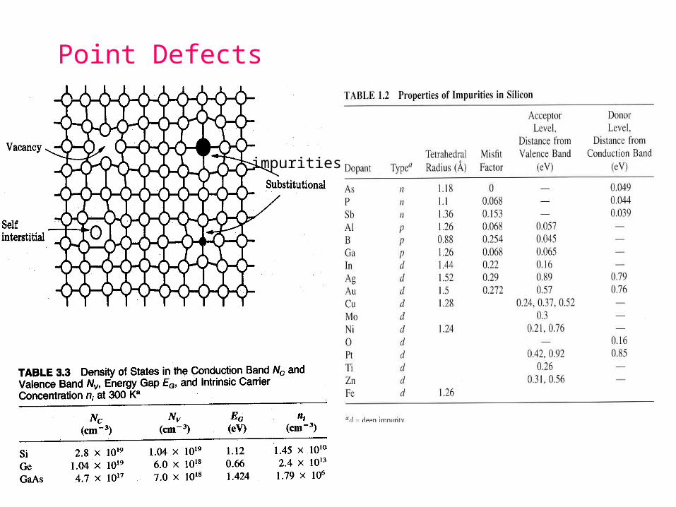
Point Defects
impurities
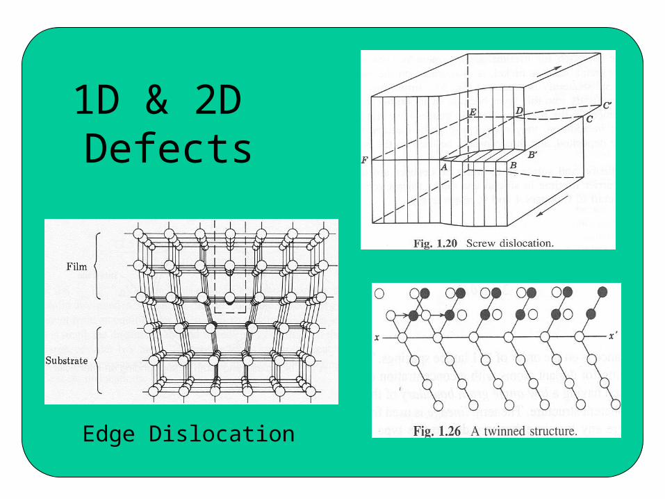
1D & 2D Defects
Edge Dislocation
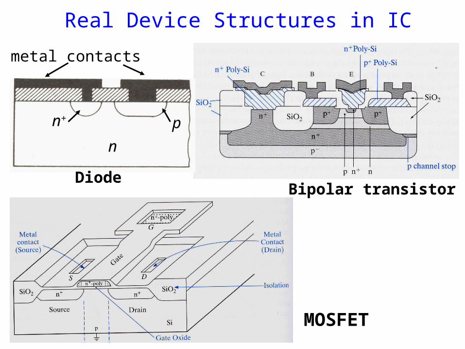
Real Device Structures in IC
MOSFET
Bipolar transistorDiode
n
n+ p
metal contacts
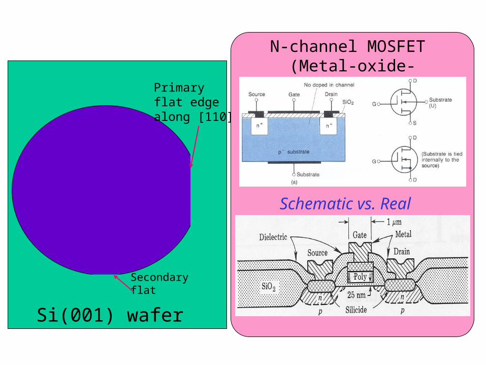
Si(001) wafer
Primary flat edgealong [110]
Secondary flat
N-channel MOSFET (Metal-oxide-semiconductor FET)
Schematic vs. Real
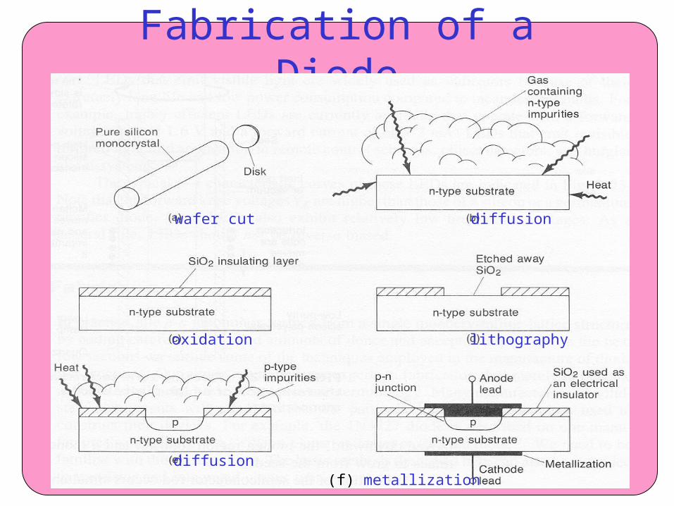
Fabrication of a Diode
wafer cut diffusion
oxidation lithography
diffusion(f) metallization
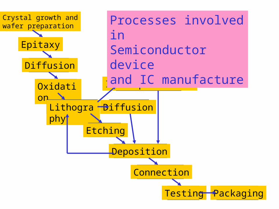
Crystal growth andwafer preparation
Diffusion
Oxidation
Lithography Diffusion
Ion implantation
Etching
Deposition
Testing Packaging
Processes involved in Semiconductor device and IC manufacture
Connection
Epitaxy