Embed Size (px)
Citation preview
Improving landfill monitoring programswith the aid of geoelectrical - imaging techniquesand geographical information systems Master’s Thesis in the Master Degree Programme, Civil Engineering
KEVIN HINE
Department of Civil and Environmental Engineering Division of GeoEngineering Engineering Geology Research GroupCHALMERS UNIVERSITY OF TECHNOLOGYGöteborg, Sweden 2005Master’s Thesis 2005:22
Space-Time Adaptive Processing in FPGAMaster of Science Thesis in Embedded Electronic System Design
SABINA FRIBERGPER PALSSON
Chalmers University of TechnologyDepartment of Computer Science and EngineeringGothenburg, Sweden, November 2012
The Authors grants to Chalmers University of Technology and University of Gothenburgthe non-exclusive right to publish the Work electronically and in a non-commercial purposemake it accessible on the Internet. The Authors warrants that they are the authors to theWork, and warrants that the Work does not contain text, pictures or other material thatviolates copyright law.
The Authors shall, when transferring the rights of the Work to a third party (for examplea publisher or a company), acknowledge the third party about this agreement. If theAuthors have signed a copyright agreement with a third party regarding the Work, theAuthors warrant hereby that they have obtained any necessary permission from this thirdparty to let Chalmers University of Technology and University of Gothenburg store theWork electronically and make it accessible on the Internet.
Space-Time Adaptive Processing in FPGAMaster of Science Thesis in Embedded Electronic System Design
Sabina F. Friberg, Per C. T. Palsson
c©Sabina F. Friberg, November 2012.c©Per C. T. Palsson, November 2012.
Examiner: Lars Bengtsson
Chalmers University of TechnologyUniversity of GothenburgDepartment of Computer Science and EngineeringSE-412 96 GoteborgSwedenTelephone + 46 (0)31-772 1000
Cover: Illustration of a fighter aircraft tracking multiple targets.
Department of Computer Science and EngineeringGoteborg, Sweden November 2012


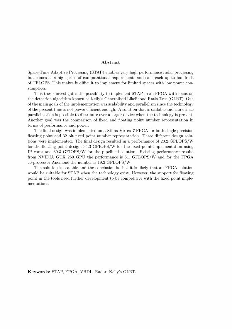
Abstract
Space-Time Adaptive Processing (STAP) enables very high performance radar processingbut comes at a high price of computational requirements and can reach up to hundredsof TFLOPS. This makes it difficult to implement for limited spaces with low power con-sumption.
This thesis investigates the possibility to implement STAP in an FPGA with focus onthe detection algorithm known as Kelly’s Generalised Likelihood Ratio Test (GLRT). Oneof the main goals of the implementation was scalability and parallelism since the technologyof the present time is not power efficient enough. A solution that is scalable and can utilizeparallelization is possible to distribute over a larger device when the technology is present.Another goal was the comparison of fixed and floating point number representation interms of performance and power.
The final design was implemented on a Xilinx Virtex-7 FPGA for both single precisionfloating point and 32 bit fixed point number representation. Three different design solu-tions were implemented. The final design resulted in a performance of 23.2 GFLOPS/Wfor the floating point design, 34.3 GFIOPS/W for the fixed point implementation usingIP cores and 39.3 GFIOPS/W for the pipelined solution. Existing performance resultsfrom NVIDIA GTX 260 GPU the performance is 5.1 GFLOPS/W and for the FPGAco-processor Anemone the number is 19.2 GFLOPS/W.
The solution is scalable and the conclusion is that it is likely that an FPGA solutionwould be suitable for STAP when the technology exist. However, the support for floatingpoint in the tools need further development to be competitive with the fixed point imple-mentations.
Keywords: STAP, FPGA, VHDL, Radar, Kelly’s GLRT.


Acknowledgments
We would like to thank our supervisors at Saab AB, Anders Ahlander and Kent Abra-hamsson and our supervisor at Chalmers University of Technology, Lars Bengtsson fortheir help and feedback throughout the project. Also, we would like to thank AndersBergaker for technical support.

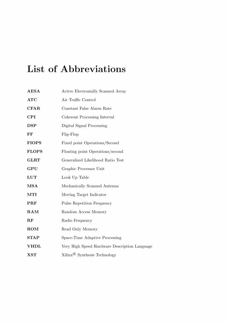
List of Abbreviations
AESA Active Electronially Scanned Array
ATC Air Traffic Control
CFAR Constant False Alarm Rate
CPI Coherent Processing Interval
DSP Digital Signal Processing
FF Flip-Flop
FIOPS Fixed point Operations/Second
FLOPS Floating point Operations/second
GLRT Generalized Likelihood Ratio Test
GPU Graphic Processor Unit
LUT Look Up Table
MSA Mechanically Scanned Antenna
MTI Moving Target Indicator
PRF Pulse Repetition Frequency
RAM Random Access Memory
RF Radio Frequency
ROM Read Only Memory
STAP Space-Time Adaptive Processing
VHDL Very High Speed Hardware Description Language
XST Xilinx R© Synthesis Technology

Contents
1 Introduction 1
1.1 Background . . . . . . . . . . . . . . . . . . . . . . . . . . . . . . . . . . . . 1
1.2 Purpose . . . . . . . . . . . . . . . . . . . . . . . . . . . . . . . . . . . . . . 2
1.3 Scope and Limitations . . . . . . . . . . . . . . . . . . . . . . . . . . . . . . 2
1.4 Method . . . . . . . . . . . . . . . . . . . . . . . . . . . . . . . . . . . . . . 3
2 Radar Fundamentals 5
2.1 Basic Radar Theory . . . . . . . . . . . . . . . . . . . . . . . . . . . . . . . 5
2.1.1 Range and Velocity Determination . . . . . . . . . . . . . . . . . . . 5
2.1.2 Active Electronically Scanned Array (AESA) . . . . . . . . . . . . . 6
2.2 Signal Processing for Radar . . . . . . . . . . . . . . . . . . . . . . . . . . . 8
2.2.1 Digital Adaptive Beamforming . . . . . . . . . . . . . . . . . . . . . 8
2.2.2 Pulse Compression . . . . . . . . . . . . . . . . . . . . . . . . . . . . 9
2.2.3 Clutter Filter . . . . . . . . . . . . . . . . . . . . . . . . . . . . . . . 9
2.2.4 Doppler Processing . . . . . . . . . . . . . . . . . . . . . . . . . . . . 9
2.2.5 Detection . . . . . . . . . . . . . . . . . . . . . . . . . . . . . . . . . 10
2.3 Space-Time Adaptive Processing . . . . . . . . . . . . . . . . . . . . . . . . 10
3 Algorithm introduction for STAP 13
3.1 Kelly’s Generalized Likelihood Ratio Test (GLRT) . . . . . . . . . . . . . . 13
3.2 Covariance Matrix . . . . . . . . . . . . . . . . . . . . . . . . . . . . . . . . 13
4 Algorithm Analysis 15
4.1 Kelly’s Generalized Likelihood Ratio Test . . . . . . . . . . . . . . . . . . . 15
4.1.1 Matrix Calculations - sHR−1 . . . . . . . . . . . . . . . . . . . . . . 15
4.1.2 Remaining parts of Kelly’s GLRT . . . . . . . . . . . . . . . . . . . 16
4.2 Covariance Matrix . . . . . . . . . . . . . . . . . . . . . . . . . . . . . . . . 16
4.3 Fixed and Floating Point Number Representation . . . . . . . . . . . . . . . 17
5 Hardware and Tools 19
5.1 Target Hardware . . . . . . . . . . . . . . . . . . . . . . . . . . . . . . . . . 19
5.2 Synthesis Tools XST and Synplify Pro . . . . . . . . . . . . . . . . . . . . . 19
5.2.1 Synthesis Attributes . . . . . . . . . . . . . . . . . . . . . . . . . . . 20
5.3 Design Suite Xilinx ISE . . . . . . . . . . . . . . . . . . . . . . . . . . . . . 20
5.4 DSP Slices, the Basic Building Block for Arithmetics . . . . . . . . . . . . . 21
5.5 Xilinx CoreGEN IP Cores . . . . . . . . . . . . . . . . . . . . . . . . . . . . 22
5.6 Technology Independence of Arithmetic Operations . . . . . . . . . . . . . . 23
i
6 Implementation of Generic Computation Units 256.1 Fixed and Floating Point Implementation . . . . . . . . . . . . . . . . . . . 25
6.1.1 Floating Point Implementation Designed for Specific Hardware . . . 256.2 Design Techniques . . . . . . . . . . . . . . . . . . . . . . . . . . . . . . . . 256.3 Complex Multiplier . . . . . . . . . . . . . . . . . . . . . . . . . . . . . . . . 266.4 Parallel Multiplier . . . . . . . . . . . . . . . . . . . . . . . . . . . . . . . . 266.5 Calculations of sHR−1s and sHR−1x . . . . . . . . . . . . . . . . . . . . . 27
6.5.1 Multiply and Accumulate for Floating Point . . . . . . . . . . . . . . 276.6 Remaining Parts of Kelly’s GLRT . . . . . . . . . . . . . . . . . . . . . . . 286.7 Memory Management . . . . . . . . . . . . . . . . . . . . . . . . . . . . . . 306.8 Functional Verification using MATLAB and Testbench . . . . . . . . . . . . 32
7 Implementation Results 337.1 Complex Multiplier . . . . . . . . . . . . . . . . . . . . . . . . . . . . . . . . 337.2 Parallel Multiplier . . . . . . . . . . . . . . . . . . . . . . . . . . . . . . . . 337.3 Calculations of sHR−1s and sHR−1x . . . . . . . . . . . . . . . . . . . . . 347.4 Final Design - Kelly’s GLRT . . . . . . . . . . . . . . . . . . . . . . . . . . 347.5 System Performance . . . . . . . . . . . . . . . . . . . . . . . . . . . . . . . 357.6 Synthesis tools . . . . . . . . . . . . . . . . . . . . . . . . . . . . . . . . . . 367.7 Scalability . . . . . . . . . . . . . . . . . . . . . . . . . . . . . . . . . . . . . 367.8 Floating Point Implementation Designed for Specific Hardware . . . . . . . 37
8 Results from other Parallel Solutions 398.1 Graphic Processor Units (GPU) . . . . . . . . . . . . . . . . . . . . . . . . . 398.2 Multi-core Processors . . . . . . . . . . . . . . . . . . . . . . . . . . . . . . 40
9 Discussion 419.1 Hardware platform . . . . . . . . . . . . . . . . . . . . . . . . . . . . . . . . 419.2 Tools . . . . . . . . . . . . . . . . . . . . . . . . . . . . . . . . . . . . . . . . 419.3 Number Representation . . . . . . . . . . . . . . . . . . . . . . . . . . . . . 429.4 Performance . . . . . . . . . . . . . . . . . . . . . . . . . . . . . . . . . . . . 439.5 Implementation of STAP on an FPGA . . . . . . . . . . . . . . . . . . . . . 43
9.5.1 Bottlenecks of the Design . . . . . . . . . . . . . . . . . . . . . . . . 44
10 Conclusion 4510.1 Design and Number Representation . . . . . . . . . . . . . . . . . . . . . . . 4510.2 Performance and Power Efficiency . . . . . . . . . . . . . . . . . . . . . . . 4510.3 Scaling . . . . . . . . . . . . . . . . . . . . . . . . . . . . . . . . . . . . . . . 45
11 Future Work 47
Bibliography 50
A Final Design Structure - Kelly’s GLRT A1
B Testbench B1
C Additional Results C1C.1 Synplify Pro against Virtex-7 . . . . . . . . . . . . . . . . . . . . . . . . . . C1C.2 Results for Virtex-5 . . . . . . . . . . . . . . . . . . . . . . . . . . . . . . . C2
ii
1. Introduction
This thesis studies parts of the Space-Time Adaptive Processing (STAP) technique forairborne radar systems. This chapter aims to give an introduction to radar systems andespecially STAP and explain why this thesis is of interest, what has been done, how andthe parts left out.
1.1 Background
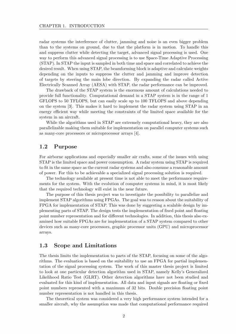
Radar systems are used for detecting and tracking objects by using an antenna to sendand receive radio waves. The basic function and design of a radar system is illustrated inFigure 1.1 where the antenna emits a radio wave generated in the transmitter. Betweentwo pulses, the receiver listens for the echo of the signal. A small part of the energy in thetransmitted radio wave is reflected off the potential target in the direction of the receiver.This small part that bounces back is to be detected among clutter, jamming and othernoise and for this, the incoming signal has to be processed to detect the target.
Transmitter
Receiver
Output to signal processing
Emitted wave
Reflected wave
Figure 1.1: Illustration of the basic principle of a radar system.
The history of radar originates in 1886 when Hertz demonstrated the reflection of radiowaves but it was not until the 1930s that the radar development accelerated [1]. AfterWorld War II the development focused on things not present or completely working in theradar systems during the war, such as the use of the Doppler effect in the moving targetindication (MTI) radar and the electronically steered phased array antenna for rapid beamsteering [2].
Applications for radar are many: Military, traffic control with radar speed meters,Air Traffic Control (ATC), navigation and ship safety among others [2]. For airborne
1
CHAPTER 1. INTRODUCTION
radar systems the interference of clutter, jamming and noise is an even bigger problemthan to the systems on ground, due to that the platform is in motion. To handle thisand suppress clutter while detecting the target, advanced signal processing is used. Oneway to perform this advanced signal processing is to use Space-Time Adaptive Processing(STAP). In STAP the input is sampled in both time and space and correlated to achieve thedesired result. When using STAP, the beamforming block is adaptive and calculate weightsdepending on the inputs to suppress the clutter and jamming and improve detectionof targets by steering the main lobe direction. By expanding the radar called ActiveElectrically Scanned Array (AESA) with STAP, the radar performance can be improved.
The drawback of the STAP system is the enormous amount of calculations needed toprovide full functionality. Computational demand in a STAP system is in the range of 1GFLOPS to 50 TFLOPS, but can easily scale up to 100 TFLOPS and above dependingon the system [3]. This makes it hard to implement the radar system using STAP in anenergy efficient way while meeting the constraints of the limited space available for thesystem in an aircraft.
While the algorithms used in STAP are extremely computational heavy, they are alsoparallelizable making them suitable for implementation on parallel computer systems suchas many-core processors or microprocessor arrays [4].
1.2 Purpose
For airborne applications and especially smaller air crafts, some of the issues with usingSTAP is the limited space and power consumption. A radar system using STAP is requiredto fit in the same space as the current radar systems and also consume a reasonable amountof power. For this to be achievable a specialized signal processing solution is required.
The technology available at present time is not able to meet the performance require-ments for the system. With the evolution of computer systems in mind, it is most likelythat the required technology will exist in the near future.
The purpose of this thesis project was to investigate the possibility to parallelize andimplement STAP algorithms using FPGAs. The goal was to reason about the suitability ofFPGA for implementation of STAP. This was done by suggesting a scalable design by im-plementing parts of STAP. The design tests the implementation of fixed point and floatingpoint number representation and for different technologies. In addition, this thesis also ex-amined how suitable FPGAs are for implementation of a STAP system compared to otherdevices such as many-core processors, graphic processor units (GPU) and microprocessorarrays.
1.3 Scope and Limitations
The thesis limits the implementation to parts of the STAP, focusing on some of the algo-rithms. The evaluation is based on the suitability to use an FPGA for partial implemen-tation of the signal processing system. The work of this master thesis project is limitedto look at one particular detection algorithm used in STAP, namely Kelly’s GeneralizedLikelihood Ratio Test (GLRT). Other detection algorithms have not been studied andevaluated for this kind of implementation. All data and input signals are floating or fixedpoint numbers represented with a maximum of 32 bits. Double precision floating pointnumber representation is not handled in this thesis.
The theoretical system was considered a very high performance system intended for asmaller aircraft, why the assumption was made that computational performance required
2
1.4. METHOD
approximately 100 TFLOPS. Also due to the limited space in the aircraft, power consump-tion was assumed to be limited. A reasonable assumption was that the power consumptionshould not exceed that of a high performance home computer, approximately 400 W.
1.4 Method
To fulfill the goals of this thesis, a thorough literature study was done to provide good basicknowledge of radar system as well as the relevant theory for the algorithm. The literaturestudy was followed by an analysis of Kelly’s GLRT detection algorithm to isolate the mostcomputational parts to evaluate the suitability for parallelization.
After determining which parts of the algorithm that would benefit the most fromparallelization, an implementation in VDHL was designed. The design was implementedby using a bottom-up approach for the ability to eliminate bottlenecks in an early stageas well as individual component testing and verification. The solutions were designed forboth fixed point and floating point number representation and implemented for two targetFPGAs, Virtex-5 and Virtex-7, focusing on the Virtex-7 device. This resulted in threeindividual designs created from the same structure. Two tools were used for synthesis,Synplify Pro and Xilinx ISE XST and the design suite Xilinx ISE was used for mapping,placement and routing of the hardware. Xilinx’s XPower was used to estimate powerconsumption. A testbench was built and used to verify the designs.
The results were evaluated and fixed point was compared to floating point to give themost efficient design. The different technologies were also compared to one another.
The structure of the report follows the work method with some basic radar theory andsignal processing for radar systems, followed by the mathematical theory behind the STAPalgorithms. The algorithms are further analysed in chapter 4 to parallelize the differentparts of the algorithm. The following part of the report is the implementation and designwork and the corresponding result. In the end, the results are compared to other parallelsolutions and discussed even further in the discussion chapter. The report ends with theconclusion and suggestion for future work.
3

CHAPTER 1. INTRODUCTION
4
2. Radar Fundamentals
This chapter deals with the relevant theory of this thesis. The first part describes basicradar theory to give a basic knowledge of radar systems used today and also to providebackground information about how the Active Electrically Scanned Array (AESA) anten-nas operates in a radar system. It is briefly described how to steer the beam by DigitalAdaptive Beamforming (adaptive DBF). The second part of the chapter describes signalprocessing for such radar systems, both in the conventional way but also elaborates onSpace-Time Adaptive Processing (STAP).
2.1 Basic Radar Theory
The word radar means, and is originally an acronym for, radio detection and ranging.Radar systems use radio waves to detect objects and determine distance as well as relativespeed. The radar system antenna emits pulses of radio waves that are reflected by theobject. Some of that energy is reflected back to the radar system. This energy is processedand used to determine both distance to the object and a potential direction and velocity ifthe object is in motion. The radar system can be designed in many different ways, usingdifferent types of antennas that can be controlled and steered in different ways.
2.1.1 Range and Velocity Determination
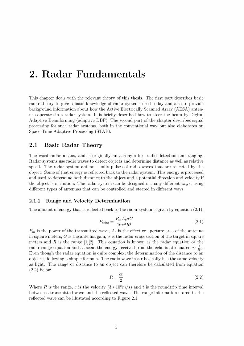
The amount of energy that is reflected back to the radar system is given by equation (2.1).
Pecho =PmAeσG
16π2R4(2.1)
Pm is the power of the transmitted wave, Ae is the effective aperture area of the antennain square meters, G is the antenna gain, σ is the radar cross section of the target in squaremeters and R is the range [1][2]. This equation is known as the radar equation or theradar range equation and as seen, the energy received from the echo is attenuated ∼ 1
R4 .Even though the radar equation is quite complex, the determination of the distance to anobject is following a simple formula. The radio wave in air basically has the same velocityas light. The range or distance to an object can therefore be calculated from equation(2.2) below.
R =ct
2(2.2)
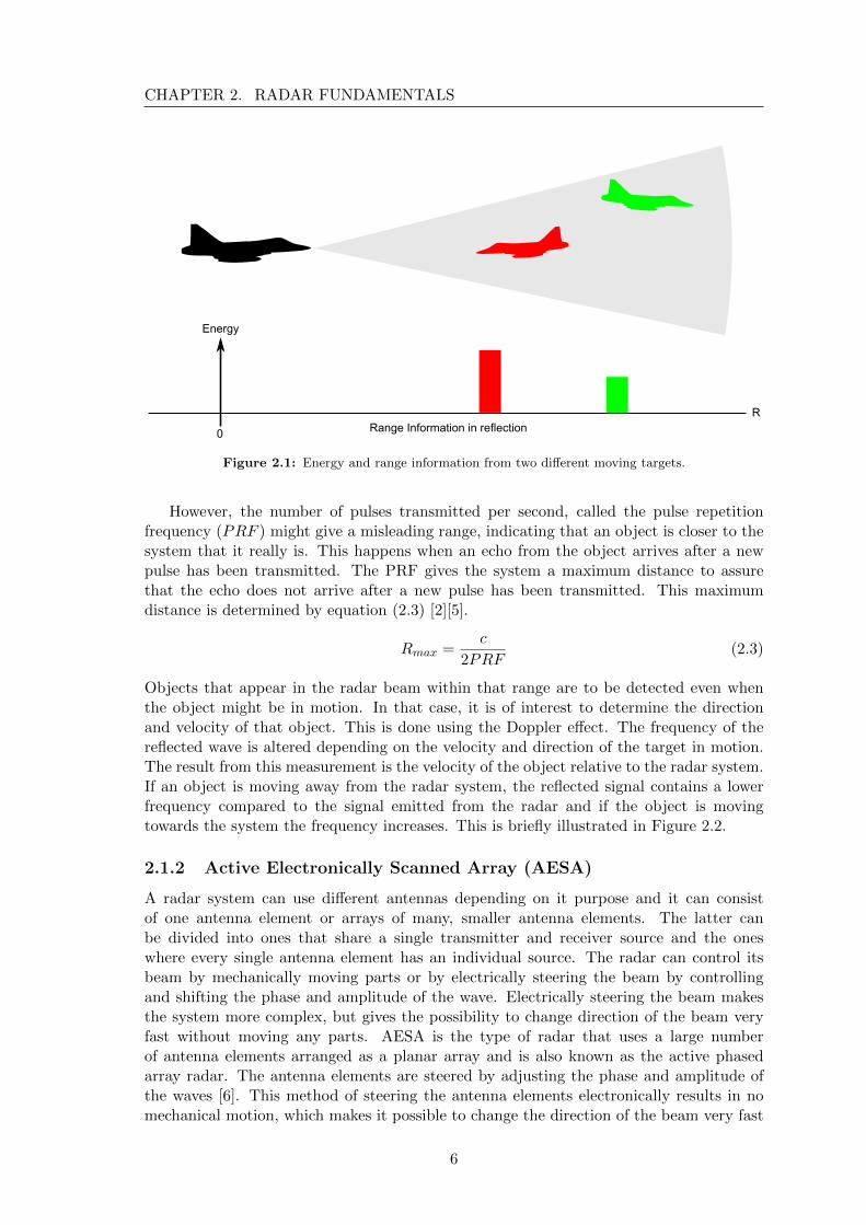
Where R is the range, c is the velocity (3 ∗ 108m/s) and t is the roundtrip time intervalbetween a transmitted wave and the reflected wave. The range information stored in thereflected wave can be illustated according to Figure 2.1.
5
CHAPTER 2. RADAR FUNDAMENTALS
Range Information in reflection0
R
Energy
Figure 2.1: Energy and range information from two different moving targets.
However, the number of pulses transmitted per second, called the pulse repetitionfrequency (PRF ) might give a misleading range, indicating that an object is closer to thesystem that it really is. This happens when an echo from the object arrives after a newpulse has been transmitted. The PRF gives the system a maximum distance to assurethat the echo does not arrive after a new pulse has been transmitted. This maximumdistance is determined by equation (2.3) [2][5].
Rmax =c
2PRF(2.3)
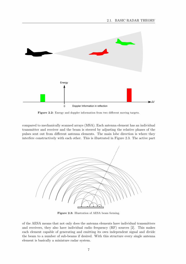
Objects that appear in the radar beam within that range are to be detected even whenthe object might be in motion. In that case, it is of interest to determine the directionand velocity of that object. This is done using the Doppler effect. The frequency of thereflected wave is altered depending on the velocity and direction of the target in motion.The result from this measurement is the velocity of the object relative to the radar system.If an object is moving away from the radar system, the reflected signal contains a lowerfrequency compared to the signal emitted from the radar and if the object is movingtowards the system the frequency increases. This is briefly illustrated in Figure 2.2.
2.1.2 Active Electronically Scanned Array (AESA)
A radar system can use different antennas depending on it purpose and it can consistof one antenna element or arrays of many, smaller antenna elements. The latter canbe divided into ones that share a single transmitter and receiver source and the oneswhere every single antenna element has an individual source. The radar can control itsbeam by mechanically moving parts or by electrically steering the beam by controllingand shifting the phase and amplitude of the wave. Electrically steering the beam makesthe system more complex, but gives the possibility to change direction of the beam veryfast without moving any parts. AESA is the type of radar that uses a large numberof antenna elements arranged as a planar array and is also known as the active phasedarray radar. The antenna elements are steered by adjusting the phase and amplitude ofthe waves [6]. This method of steering the antenna elements electronically results in nomechanical motion, which makes it possible to change the direction of the beam very fast
6
2.1. BASIC RADAR THEORY
Doppler Information in reflection
Energy
0
f
Figure 2.2: Energy and doppler information from two different moving targets.
compared to mechanically scanned arrays (MSA). Each antenna element has an individualtransmitter and receiver and the beam is steered by adjusting the relative phases of thepulses sent out from different antenna elements. The main lobe direction is where theyinterfere constructively with each other. This is illustrated in Figure 2.3. The active part
Figure 2.3: Illustration of AESA beam forming.
of the AESA means that not only does the antenna elements have individual transmittersand receivers, they also have individual radio frequency (RF) sources [2]. This makeseach element capable of generating and emitting its own independent signal and dividethe beam to a number of sub-beams if desired. With this structure every single antennaelement is basically a miniature radar system.
7
CHAPTER 2. RADAR FUNDAMENTALS
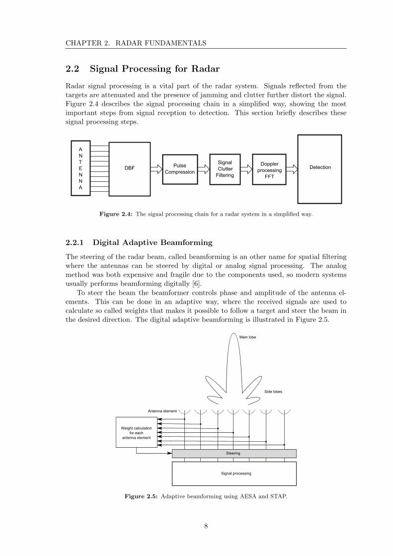
2.2 Signal Processing for Radar
Radar signal processing is a vital part of the radar system. Signals reflected from thetargets are attenuated and the presence of jamming and clutter further distort the signal.Figure 2.4 describes the signal processing chain in a simplified way, showing the mostimportant steps from signal reception to detection. This section briefly describes thesesignal processing steps.
DBFSignal Clutter
Filtering
Pulse Compression
Dopplerprocessing
FFT
Detection
ANTENNA
Figure 2.4: The signal processing chain for a radar system in a simplified way.
2.2.1 Digital Adaptive Beamforming
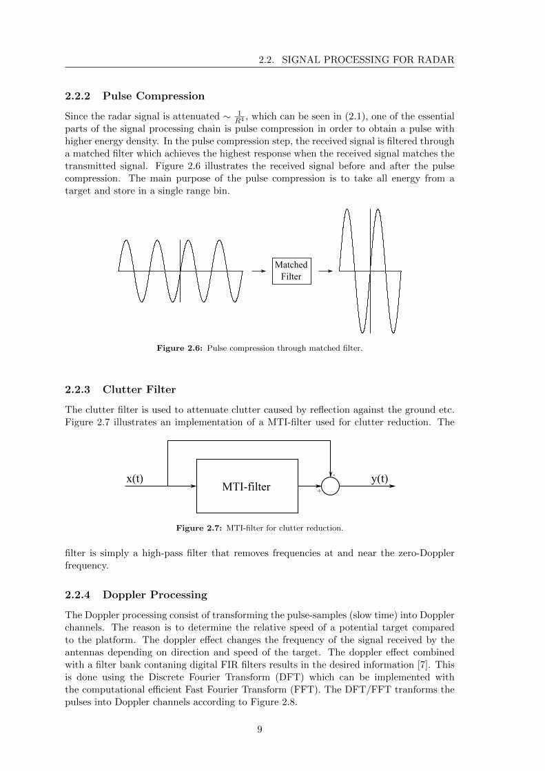
The steering of the radar beam, called beamforming is an other name for spatial filteringwhere the antennas can be steered by digital or analog signal processing. The analogmethod was both expensive and fragile due to the components used, so modern systemsusually performs beamforming digitally [6].
To steer the beam the beamformer controls phase and amplitude of the antenna el-ements. This can be done in an adaptive way, where the received signals are used tocalculate so called weights that makes it possible to follow a target and steer the beam inthe desired direction. The digital adaptive beamforming is illustrated in Figure 2.5.
Signal processing
Weight calculationfor each
antenna element
Steering
Main lobe
Side lobes
Antenna element
Figure 2.5: Adaptive beamforming using AESA and STAP.
8
2.2. SIGNAL PROCESSING FOR RADAR
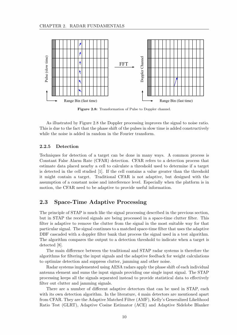
2.2.2 Pulse Compression
Since the radar signal is attenuated ∼ 1R4 , which can be seen in (2.1), one of the essential
parts of the signal processing chain is pulse compression in order to obtain a pulse withhigher energy density. In the pulse compression step, the received signal is filtered througha matched filter which achieves the highest response when the received signal matches thetransmitted signal. Figure 2.6 illustrates the received signal before and after the pulsecompression. The main purpose of the pulse compression is to take all energy from atarget and store in a single range bin.
MatchedFilter
Figure 2.6: Pulse compression through matched filter.
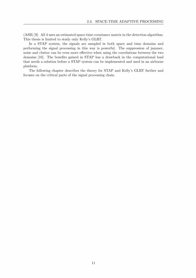
2.2.3 Clutter Filter
The clutter filter is used to attenuate clutter caused by reflection against the ground etc.Figure 2.7 illustrates an implementation of a MTI-filter used for clutter reduction. The
MTI-filterx(t)
+
- y(t)
Figure 2.7: MTI-filter for clutter reduction.
filter is simply a high-pass filter that removes frequencies at and near the zero-Dopplerfrequency.
2.2.4 Doppler Processing
The Doppler processing consist of transforming the pulse-samples (slow time) into Dopplerchannels. The reason is to determine the relative speed of a potential target comparedto the platform. The doppler effect changes the frequency of the signal received by theantennas depending on direction and speed of the target. The doppler effect combinedwith a filter bank contaning digital FIR filters results in the desired information [7]. Thisis done using the Discrete Fourier Transform (DFT) which can be implemented withthe computational efficient Fast Fourier Transform (FFT). The DFT/FFT tranforms thepulses into Doppler channels according to Figure 2.8.
9
CHAPTER 2. RADAR FUNDAMENTALS
Range Bin (fast time)
Pul
se (
slow
tim
e)
Range Bin (fast time)
Dop
pler
Cha
nnel
FFT
Figure 2.8: Transformation of Pulse to Doppler channel.
As illustrated by Figure 2.8 the Doppler processing improves the signal to noise ratio.This is due to the fact that the phase shift of the pulses in slow time is added constructivelywhile the noise is added in random in the Fourier transform.
2.2.5 Detection
Techniques for detection of a target can be done in many ways. A common process isConstant False Alarm Rate (CFAR) detection. CFAR refers to a detection process thatestimate data placed nearby a cell to calculate a threshold used to determine if a targetis detected in the cell studied [1]. If the cell contains a value greater than the thresholdit might contain a target. Traditional CFAR is not adaptive, but designed with theassumption of a constant noise and interference level. Especially when the platform is inmotion, the CFAR need to be adaptive to provide useful information.
2.3 Space-Time Adaptive Processing
The principle of STAP is much like the signal processing described in the previous section,but in STAP the received signals are being processed in a space-time clutter filter. Thisfilter is adaptive to remove the clutter from the signal in the most suitable way for thatparticular signal. The signal continues to a matched space-time filter that uses the adaptiveDBF cascaded with a doppler filter bank that process the signal used in a test algorithm.The algorithm compares the output to a detection threshold to indicate when a target isdetected [8].
The main difference between the traditional and STAP radar systems is therefore thealgorithms for filtering the input signals and the adaptive feedback for weight calculationsto optimize detection and suppress clutter, jamming and other noise.
Radar systems implemented using AESA radars apply the phase shift of each individualantenna element and sums the input signals providing one single input signal. The STAPprocessing keeps all the signals separated instead to provide statistical data to effectivelyfilter out clutter and jamming signals.
There are a number of different adaptive detectors that can be used in STAP, eachwith its own detection algorithm. In the literature, 4 main detectors are mentioned apartfrom CFAR. They are the Adaptive Matched Filter (AMF), Kelly’s Generalized LikelihoodRatio Test (GLRT), Adaptive Cosine Estimator (ACE) and Adaptive Sidelobe Blanker
10
2.3. SPACE-TIME ADAPTIVE PROCESSING
(ASB) [9]. All 4 uses an estimated space-time covariance matrix in the detection algorithm.This thesis is limited to study only Kelly’s GLRT.
In a STAP system, the signals are sampled in both space and time domains andperforming the signal processing in this way is powerful. The suppression of jammer,noise and clutter can be even more effective when using the correlations between the twodomains [10]. The benefits gained in STAP has a drawback in the computational loadthat needs a solution before a STAP system can be implemented and used in an airborneplatform.
The following chapter describes the theory for STAP and Kelly’s GLRT further andfocuses on the critical parts of the signal processing chain.
11

CHAPTER 2. RADAR FUNDAMENTALS
12
3. Algorithm introduction forSTAP
This chapter further discusses the mathematical theory used in the computational algo-rithms of STAP and explains the different steps of Kelly’s GLRT detection algorithm.First a thorough description of Kelly’s GLRT is presented, followed by a description ofthe estimated covariance matrix used in STAP.
3.1 Kelly’s Generalized Likelihood Ratio Test (GLRT)
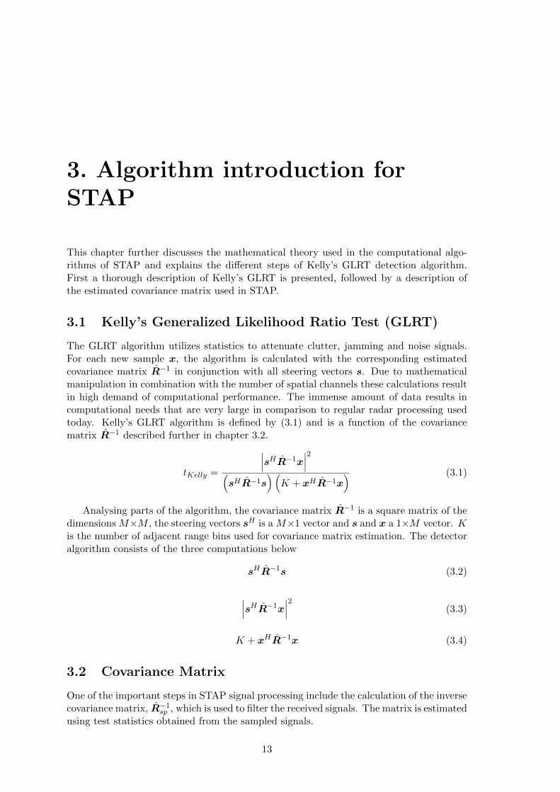
The GLRT algorithm utilizes statistics to attenuate clutter, jamming and noise signals.For each new sample x, the algorithm is calculated with the corresponding estimatedcovariance matrix R−1 in conjunction with all steering vectors s. Due to mathematicalmanipulation in combination with the number of spatial channels these calculations resultin high demand of computational performance. The immense amount of data results incomputational needs that are very large in comparison to regular radar processing usedtoday. Kelly’s GLRT algorithm is defined by (3.1) and is a function of the covariancematrix R−1 described further in chapter 3.2.
tKelly =
∣∣∣sHR−1x∣∣∣2(
sHR−1s)(
K + xHR−1x) (3.1)
Analysing parts of the algorithm, the covariance matrix R−1 is a square matrix of thedimensions M×M , the steering vectors sH is a M×1 vector and s and x a 1×M vector. Kis the number of adjacent range bins used for covariance matrix estimation. The detectoralgorithm consists of the three computations below
sHR−1s (3.2)
∣∣∣sHR−1x∣∣∣2 (3.3)
K + xHR−1x (3.4)
3.2 Covariance Matrix
One of the important steps in STAP signal processing include the calculation of the inversecovariance matrix, R−1
sp , which is used to filter the received signals. The matrix is estimatedusing test statistics obtained from the sampled signals.
13
CHAPTER 3. ALGORITHM INTRODUCTION FOR STAP
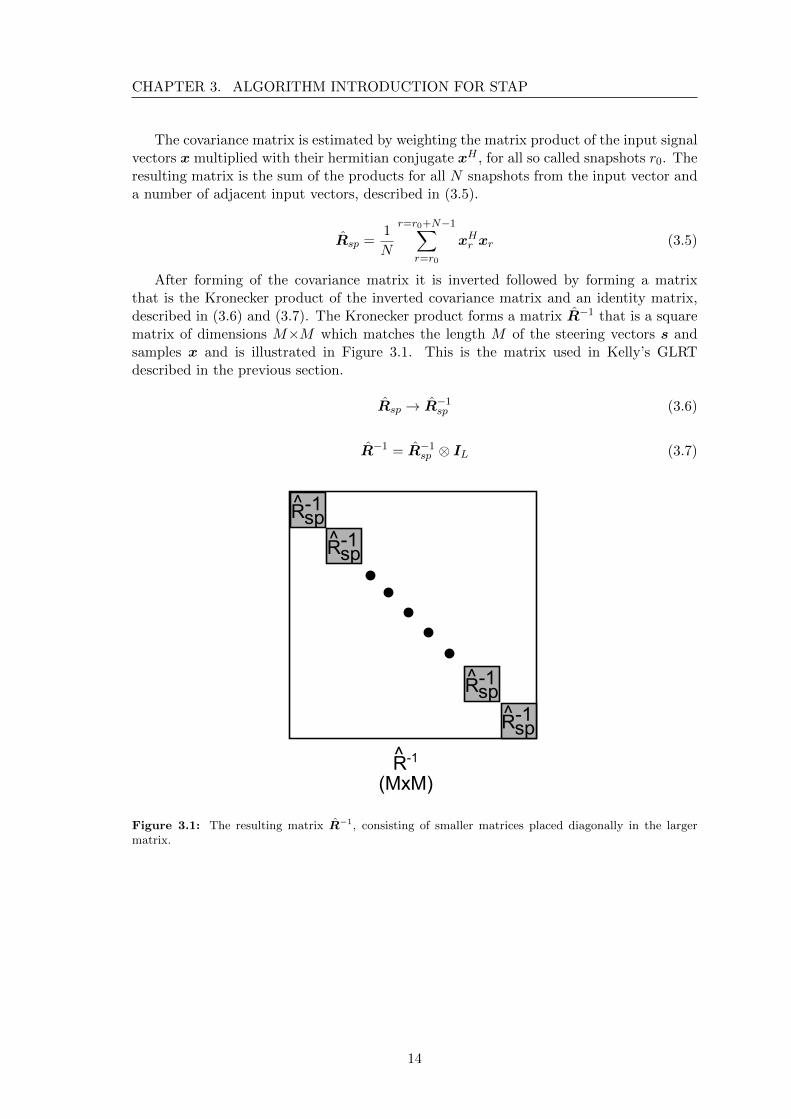
The covariance matrix is estimated by weighting the matrix product of the input signalvectors x multiplied with their hermitian conjugate xH , for all so called snapshots r0. Theresulting matrix is the sum of the products for all N snapshots from the input vector anda number of adjacent input vectors, described in (3.5).
Rsp =1
N
r=r0+N−1∑r=r0
xHr xr (3.5)
After forming of the covariance matrix it is inverted followed by forming a matrixthat is the Kronecker product of the inverted covariance matrix and an identity matrix,described in (3.6) and (3.7). The Kronecker product forms a matrix R−1 that is a squarematrix of dimensions M×M which matches the length M of the steering vectors s andsamples x and is illustrated in Figure 3.1. This is the matrix used in Kelly’s GLRTdescribed in the previous section.
Rsp → R−1sp (3.6)
R−1 = R−1sp ⊗ IL (3.7)
R-1^
R-1^sp
R-1^sp
R-1^sp
R-1^sp
(MxM)
Figure 3.1: The resulting matrix R−1, consisting of smaller matrices placed diagonally in the largermatrix.
14
4. Algorithm Analysis
This chapter examines possible ways to parallelize different parts of the algorithm. Thealgorithm is fortunately very parallelizable and uses relatively few input values for outputcalculation, which limits memory bandwidth when implementing for an FPGA since mostof the data can be kept on chip. For the implementation to be applicable and functionalit needs to be scalable as well as able to efficiently use most of the available resources onthe chip. The investigations are made to make the most suitable choice of the parts thatare intended for implementation.
4.1 Kelly’s Generalized Likelihood Ratio Test
Looking at the equations in chapter 3.1, it is obvious that Kelly’s GLRT detection algo-rithm is very parallelizable. However, the calculations need to be done for every combi-nation of data input samples x and steering vectors s. In addition to this, the covariancematrix needs to be updated with a certain frequency according to (3.5) in section 3.2.
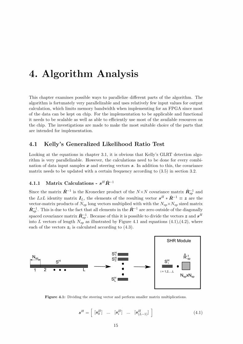
4.1.1 Matrix Calculations - sHR−1
Since the matrix R−1 is the Kronecker product of the N×N covariance matrix R−1sp and
the LxL identity matrix IL, the elements of the resulting vector sH ∗ R−1 ≡ z are thevector-matrix products of Nsp long vectors multiplied with with the Nsp×Nsp sized matrix
R−1sp . This is due to the fact that all elements in the R−1 are zero outside of the diagonally
spaced covariance matrix R−1sp . Because of this it is possible to divide the vectors z and sH
into L vectors of length Nsp as illustrated by Figure 4.1 and equations (4.1),(4.2), whereeach of the vectors zi is calculated according to (4.3).
Nsp
SH
1 2 L
R-1^sp
NspxNsp
SH
SHR Module
SH
SH
SH
1
2
L
i
i = 1,2,...,L
Figure 4.1: Dividing the steering vector and perform smaller matrix multiplications.
sH =[
[sH0 ] ... [sHi ] ... [sH(L−1)]]
(4.1)
15
CHAPTER 4. ALGORITHM ANALYSIS
z =[
[z0] ... [zi] ... [z(L−1)]]
(4.2)
zi = sHi R−1sp (4.3)
This makes it possible to divide the calculation of (4.2) into a subset of matrix calcula-tions for the partial vectors sHi , where each of the vectors are multiplied with the covariancematrix. By dividing the calculation of an entire matrix in this way, it is possible to paral-lelize and reuse data by performing several calculations using the same covariance matrixin parallel.
Another way to parallelize the calculations are by performing several of the multiplica-tions for one single matrix at the same time, either by multiplying one row of the matrixwith the corresponding element in the vector or multiplying one vector column by columnin the matrix.
Using the first approach would be to focus on one row in R−1sp and multiplying with
the corresponding element in sHi at the same time. After M iterations all multiplicationsare done and the resulting vector is calculated by adding the product elements from thesame column in R−1. The Nsp first elements in z will be presented at the same time, anda new block of Nsp elements will arrive after Nsp iterations of multiplying and adding theproducts together.
If the parallelization instead is designed after the columns in R−1sp , the multiplication
can be performed for all elements of a vector sHi in parallel, performing all multiplicationsneeded for an element in z. This results in a new element ready each iteration consistingof the Nsp multiplications followed by accumulation the products. The resulting vector zneeds M iterations using this method. The only thing that differ is that a new elementis calculated each iteration. Figure 4.1 illustrates how this matrix multiplication can bedivided by performing subsets of multiplications.
Using either one of the two methods described above, it is possible to parallelize it evenfurther. This can be done by performing all multiplications done to the same column orrow, at the same time, which would correspond to the entire vector matrix multiplicationin parallel.
4.1.2 Remaining parts of Kelly’s GLRT
The products of sHR−1s and sHR−1x result in a scalars. The multiplications are possibleto perform in parallel, but are not performance critical operations for the algorithm sincethe computational load for these operations are not that heavy compared to the sHR−1
described in section 4.1.1.
The last part of the GLRT algorithm is K + xHR−1x. All steering vectors are to beused for every single input data x, why this step is only to be calculated one time andthen can be kept constant for the rest of the calculations. This is a result from having alarge number of steering vectors that all shall be applied on the input data. The resultingproduct of this calculation is also a scalar due to multiplication with the conjugate.
4.2 Covariance Matrix
The covariance matrix Rsp and the inverted matrix R−1sp is described in section 3.2. Each
matrix product constituting the final matrix Rsp is simple to parallelize since it is simply
16
4.3. FIXED AND FLOATING POINT NUMBER REPRESENTATION
N×N products of N+N input values according to equation (3.5). In practice, the esti-mation of the covariance matrix is done in blocks of samples xr. Due to a relatively smallamount of calculations, this implies that the computational load for the covariance matrixand its inverse is quite small compared to the following steps of STAP and thus, is notfurther analyzed in this thesis.
4.3 Fixed and Floating Point Number Representation
The choice of fixed or floating point number representation is also of importance whenworking with digital signal processing. When representing the data in a specific number ofbits, this may result in some differences that the designer needs to be aware of. Floatingpoint arithmetics provide much higher dynamic range and precision, especially for smallnumbers, compared to fixed point. Due to the ”fixed” placement of the decimal point inthe use of fixed point, the gaps between two adjacent numbers can be larger comparedto floating point. When performing calculations in the digital signal processing the resultmust be rounded to the nearest value in the number representation used. This yields forlarger rounding errors when using the fixed point number representation [11].
17

CHAPTER 4. ALGORITHM ANALYSIS
18
5. Hardware and Tools
Depending on the target hardware and the tools used for implementation, the results fromthe same design can differ. Therefore, it is of importance to have knowledge about thetools and technology used. There are a number of vendors on the FPGA market andthis chapter describes the target hardware for this design as well as the tools used forsynthesizing and mapping the design onto the specific target hardware.
5.1 Target Hardware
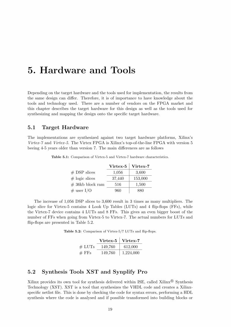
The implementations are synthesized against two target hardware platforms, Xilinx’sVirtex-7 and Virtex-5. The Virtex FPGA is Xilinx’s top-of-the-line FPGA with version 5beeing 4-5 years older than version 7. The main differences are as follows
Table 5.1: Comparison of Virtex-5 and Virtex-7 hardware characteristics.
Virtex-5 Virtex-7
# DSP slices 1,056 3,600
# logic slices 37,440 153,000
# 36kb block ram 516 1,500
# user I/O 960 880
The increase of 1,056 DSP slices to 3,600 result in 3 times as many multipliers. Thelogic slice for Virtex-5 contains 4 Look Up Tables (LUTs) and 4 flip-flops (FFs), whilethe Virtex-7 device contains 4 LUTs and 8 FFs. This gives an even bigger boost of thenumber of FFs when going from Virtex-5 to Virtex-7. The actual numbers for LUTs andflip-flops are presented in Table 5.2.
Table 5.2: Comparison of Virtex-5/7 LUTs and flip-flops.
Virtex-5 Virtex-7
# LUTs 149,760 612,000
# FFs 149,760 1,224,000
5.2 Synthesis Tools XST and Synplify Pro
Xilinx provides its own tool for synthesis delivered within ISE, called Xilinx R© SynthesisTechnology (XST). XST is a tool that synthesizes the VHDL code and creates a Xilinx-specific netlist file. This is done by checking the code for syntax errors, performing a HDLsynthesis where the code is analysed and if possible transformed into building blocks or
19
CHAPTER 5. HARDWARE AND TOOLS
macros (MUXes, RAMs, adders and subtracters)[12]. In this step of the synthesis XSTalso performs a resource sharing check to reduce the amount of macros and increase theclock frequency while reducing the area. When this is done, a low level optimization isperformed. In this step XST transform the design created in the HDL synthesis to atechnology-specific implementation. The tool is to be used for Xilinx platforms, such asVirtex-5 and Virtex-7. The drawback of this tool is that the design becomes technologydependent and it is not possible to use this netlist on platforms from other vendors.
If Synopsys Synplify Pro is used for synthesis instead, the result is a design with a multi-FPGA vendor support. Synplify Pro also checks the code for syntax errors before usingthe Behavior Extracting Synthesis Technology (BESTTM) algorithm to find structuressuch as RAMs, MUXes and arithmetic operators and turn them into building blocks ormacros, just like XST. The design is optimized and finally mapped to technology-specificcomponents. When this is done, it generates a netlist used for placement and routing.The advantage of Synplify Pro is that it it possible to use the same tool for synthesis evenwhen the design is to be mapped onto another technology.
The two tools use different algorithms when performing the synthesis and optimization,and even when the same design is synthesised and to be mapped to the same targetplatform, the result after synthesis can differ.
5.2.1 Synthesis Attributes
For the ability to control which logic elements are inferred when writing VHDL code,synthesis attributes can be set to force the synthesis tool to use a specific kind of logicelement. Synthesis attributes set constraints to force the synthesis tool to optimize andtranslate a piece of HDL code or a complete design in a specified way. To use the attributesin an efficient way, the designer needs knowledge of both the hardware target as well asthe synthesis tool. By using attributes, the designer can specify how the synthesis toolshould translate a certain piece of code [13]. If the designer wants to implement a specificcomponent on a DSP slice instead of logic to increase speed the use dsp48 attribute forXST can be used [14]. For Synplify Pro the attribute is called syn dspstyle when designingwith Xilinx [15]. As an other example Synplify Pro has difficulties inferring shift registersand generates slow logic for Xilinx devices. By setting an attribute to infer a XilinxSRL primitive this problem can be avoided. Xilinx XST tool can also for instance moveregisters across connected DSP units in an unfavorable way, which also can be avoided bysetting synthesis attributes. By using attributes the designer can optimize the design fora certain purpose and gaining a better result from a tool that usually is not optimal forthis design.
5.3 Design Suite Xilinx ISE
MAP and PAR are programs in the design suite Xilinx ISE. The tool supports the Virtex-7platform and is able to generate bitfiles to this hardware. These programs map the designto the hardware and place and route the design. There are a number of options that thedesigner need to consider to make the tool map, place and route the design in the mostefficient way. In a design where speed is of importance, some of these options can be setto make the tool optimize for speed. An example is the overall effort level that can be setto high when running PAR. The runtime during PAR will then increase, but the qualityof the result will be better in the aspect of timing. The PAR is set to place and route thedesign based on timing constraints set in a constraints file. A design with high demands
20
5.4. DSP SLICES, THE BASIC BUILDING BLOCK FOR ARITHMETICS
on speed might have a very short period time set as a constraint and one risk with thetool is that it draws the conclusion that it is not possible to meet the constraints. Thismight lead to the tool basically giving up. If the timing constraints are set to a slightlyhigher period time, the maximum frequency can be higher because the tool does not giveup as easily in that case.
Xilinx’s tool XPower which is also a part of ISE has been used for estimation of powerconsumption.
5.4 DSP Slices, the Basic Building Block for Arithmetics
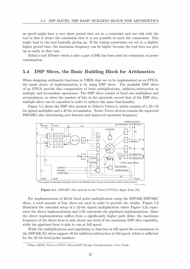
When designing arithmetic functions in VHDL that are to be implemented on an FPGA,the usual choice of implementation is by using DSP slices. The available DSP slicesof an FPGA provide fast computation of both multiplications, addition/subtraction ormultiply and accumulate operations. The DSP slices consist of fixed size multipliers andaccumulators, so when the number of bits in the operands exceed that of the DSP slice,multiple slices can be cascaded in order to achieve the same functionality.
Figure 5.1 shows the DSP slice present in Xilinx’s Virtex-5, which consists of a 25×18bit signed multiplier and a 48 bit accumulator. Newer Virtex devices contain the improvedDSP48E1 slice introducing new features and improved operation frequency.
X
17-Bit Shift
17-Bit Shift
0
Y
Z
10
0
48
48
18
4
3
48
2530
BCOUT*
BCIN* ACIN*
OPMODE
PCIN*
MULTSIGNIN*
PCOUT*
CARRYCASCOUT*
MULTSIGNOUT*
CREG/C Bypass/Mask
CARRYCASCIN*
CARRYIN
CARRYINSEL
ACOUT* A:B
ALUMODE
B
B
A
C
B
M
P
PP
C
25 X 18
A A
PATTERNDETECT
PATTERNBDETECT
CARRYOUT
UG193_c1_01_032806
4
7
48
4830
18
30
18
P
P
*These signals are dedicated routing paths internal to the DSP48E column. They are not accessible via fabric routing resources.
Figure 5.1: DSP48E1 slice present in the Virtex-5 FPGAs, figure from [16].
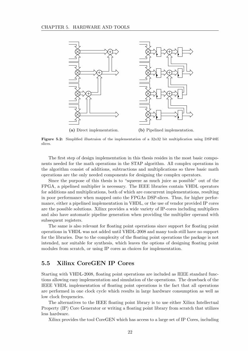
For implementation of 32-bit fixed point multiplication using the DSP48E/DSP48E1slices, a total amount of four slices are used in order to provide the results. Figure 5.2illustrates the cascaded setup of a 32-bit signed multiplication where Figure 5.2a repre-sents the direct implementation and 5.2b represents the pipelined implementation. Sincethe direct implementation suffers from a significantly higher path delay, the maximumfrequency of the direct form is only about one sixth of the maximum DSP slice capability,while the pipelined form is able to run at full speed.
While the multiplications need pipelining to function at full speed the accumulators inthe DSP48E/E1 slices support 48 bit addition/subtraction at full speed, which is sufficientfor the 32 bit fixed point numbers.
1Xilinx (2012) Virtex-5 FPGA XtremeDSP Design Considerations, User Guide.
21
CHAPTER 5. HARDWARE AND TOOLS
(a) Direct implementation. (b) Pipelined implementation.
Figure 5.2: Simplified illustraion of the implementation of a 32x32 bit multiplication using DSP48Eslices.
The first step of design implementation in this thesis resides in the most basic compo-nents needed for the math operations in the STAP algorithm. All complex operations inthe algorithm consist of additions, subtractions and multiplications so three basic mathoperations are the only needed components for designing the complex operators.
Since the purpose of this thesis is to “squeeze as much juice as possible” out of theFPGA, a pipelined multiplier is necessary. The IEEE libraries contain VHDL operatorsfor additions and multiplications, both of which are concurrent implementations, resultingin poor performance when mapped onto the FPGAs DSP-slices. Thus, for higher perfor-mance, either a pipelined implementation in VHDL, or the use of vendor provided IP coresare the possible solutions. Xilinx provides a wide variety of IP-cores including multipliersand also have automatic pipeline generation when providing the multiplier operand withsubsequent registers.
The same is also relevant for floating point operations since support for floating pointoperations in VHDL was not added until VHDL-2008 and many tools still have no supportfor the libraries. Due to the complexity of the floating point operations the package is notintended, nor suitable for synthesis, which leaves the options of designing floating pointmodules from scratch, or using IP cores as choices for implementation.
5.5 Xilinx CoreGEN IP Cores
Starting with VHDL-2008, floating point operations are included as IEEE standard func-tions allowing easy implementation and simulation of the operations. The drawback of theIEEE VHDL implementation of floating point operations is the fact that all operationsare performed in one clock cycle which results in large hardware consumption as well aslow clock frequencies.
The alternatives to the IEEE floating point library is to use either Xilinx IntellectualProperty (IP) Core Generator or writing a floating point library from scratch that utilizesless hardware.
Xilinx provides the tool CoreGEN which has access to a large set of IP Cores, including
22
5.6. TECHNOLOGY INDEPENDENCE OF ARITHMETIC OPERATIONS
floating point operations. The hardware can be instantiated with generic input widths andlatency for the output. With higher latency the component uses less hardware betweenregisters and is able to operate at higher clock frequency. The drawback of using CoreGENis that the design becomes technology dependent. By using Xilinx CoreGEN, the designcan only be implemented on a Xilinx FPGA. Also, the core generated for one hardwareplatform, for example Virtex-5 is not guaranteed to work for the next generation. Thismeans that depending on which target hardware platform the design is implemented on,the generated cores differ from each other. The generated cores for the designs in thisthesis are optimized for speed and have full usage of DSP slices.
5.6 Technology Independence of Arithmetic Operations
FPGA vendors usually complement their hardware with IP cores for various arithmeticoperations utilizing the available DSP-slices, as well as through inference by using VHDLoperators. Both Xilinx’s XST and Altera’s Quartus support automatic pipelining byadding registers prior to or after the VHDL math operator [14][17]. By reusing the im-plementations of the math components, the design can be made relatively technologyindependent. Only the base components need replacing which is made easy with IP corecomponents and pipelining support in synthesis tools. Since the more complex math oper-ations consist of the multiplication and accumulation those are the only two componentsnecessary to replace when moving between platforms.
When designing components with high requirements on both performance and chiputilization it becomes harder to implement a solution that is truly technology indepen-dent. When implementing multipliers and accumulators the demand on high throughputmakes pipe-lining a requirement which can be difficult to implement in an optimal wayfor technology independence.
23

CHAPTER 5. HARDWARE AND TOOLS
24
6. Implementation of GenericComputation Units
One of the main directives of the hardware based algorithm is the scalability of the solutionso that the implementation can be scaled to problems of different sizes as well as differenthardware platforms. By designing the solution based on generics and with scalability asa directive the solutions can be designed efficiently. The final implementation consists ofthree different solutions with drawbacks and advantages of their own.
6.1 Fixed and Floating Point Implementation
One important parameter of the design is the choice of number representation. As men-tioned in section 4.3, the floating point number representation provides higher dynamicrange as well as precision compared to fixed point number representation. However, dueto the complex structure of floating point number representation the calculations requiresubstantially more logic and delays than fixed point. In this thesis work the designs forboth 32 bits fixed point and single precision floating point are considered and compared.
6.1.1 Floating Point Implementation Designed for Specific Hardware
The base components were also designed for a floating point number representation of24 bits in total. Out of those 24 bits, 17 are used for the mantissa and 7 for the expo-nent. This is of interest due to the reduced amount of hardware used. The DSP slicedescribed in section 5.4 consists of one 25×18 bit signed multiplier so when using thisnumber representation only one DSP slice is needed for the 17 bit mantissa multiplicationinstead of two when implementing single precision number representation. Depending onrequirements for signal to noise ratio and the dynamic range of the system, a scaled downimplementation can reduce the needed amount of hardware significantly.
6.2 Design Techniques
As mentioned in section 5.5, Xilinx provides designers with IP cores designed for specificpurposes. Using Xilinx CoreGEN IP cores is effective and it does not take many man hoursto implement a design using the cores. In this thesis work the floating point implementationuses IP cores from Xilinx CoreGEN, while the fixed point designs are implemented in twodifferent ways. The first one uses IP cores in the design while the other one is designed tosuit the hardware in a pipelined structure and written from scratch. The latter is furtheron called fixed point Non-Technology Dependent (NTD).
25
CHAPTER 6. IMPLEMENTATION OF GENERIC COMPUTATION UNITS
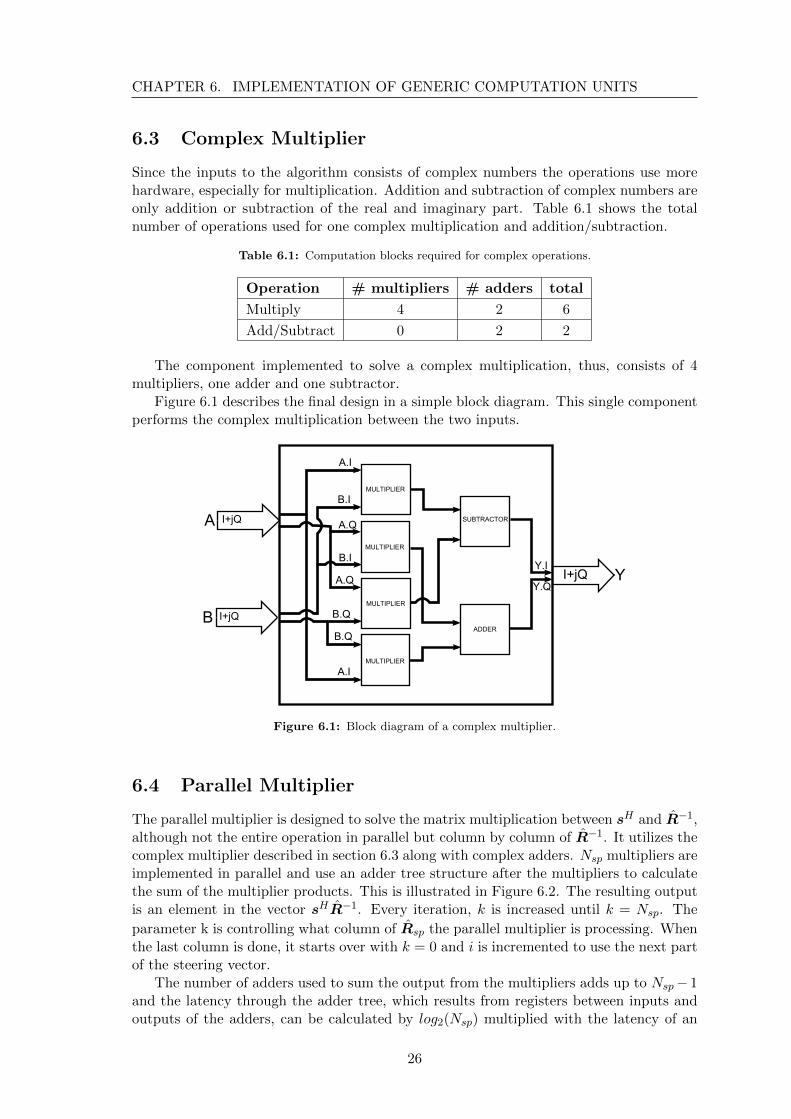
6.3 Complex Multiplier
Since the inputs to the algorithm consists of complex numbers the operations use morehardware, especially for multiplication. Addition and subtraction of complex numbers areonly addition or subtraction of the real and imaginary part. Table 6.1 shows the totalnumber of operations used for one complex multiplication and addition/subtraction.
Table 6.1: Computation blocks required for complex operations.
Operation # multipliers # adders total
Multiply 4 2 6
Add/Subtract 0 2 2
The component implemented to solve a complex multiplication, thus, consists of 4multipliers, one adder and one subtractor.
Figure 6.1 describes the final design in a simple block diagram. This single componentperforms the complex multiplication between the two inputs.
I+jQ
I+jQ
A
B
A.I
A.I
A.Q
A.Q
B.Q
B.Q
SUBTRACTOR
I+jQ YY.I
Y.Q
B.I
B.I
MULTIPLIER
MULTIPLIER
MULTIPLIER
MULTIPLIER
ADDER
Figure 6.1: Block diagram of a complex multiplier.
6.4 Parallel Multiplier
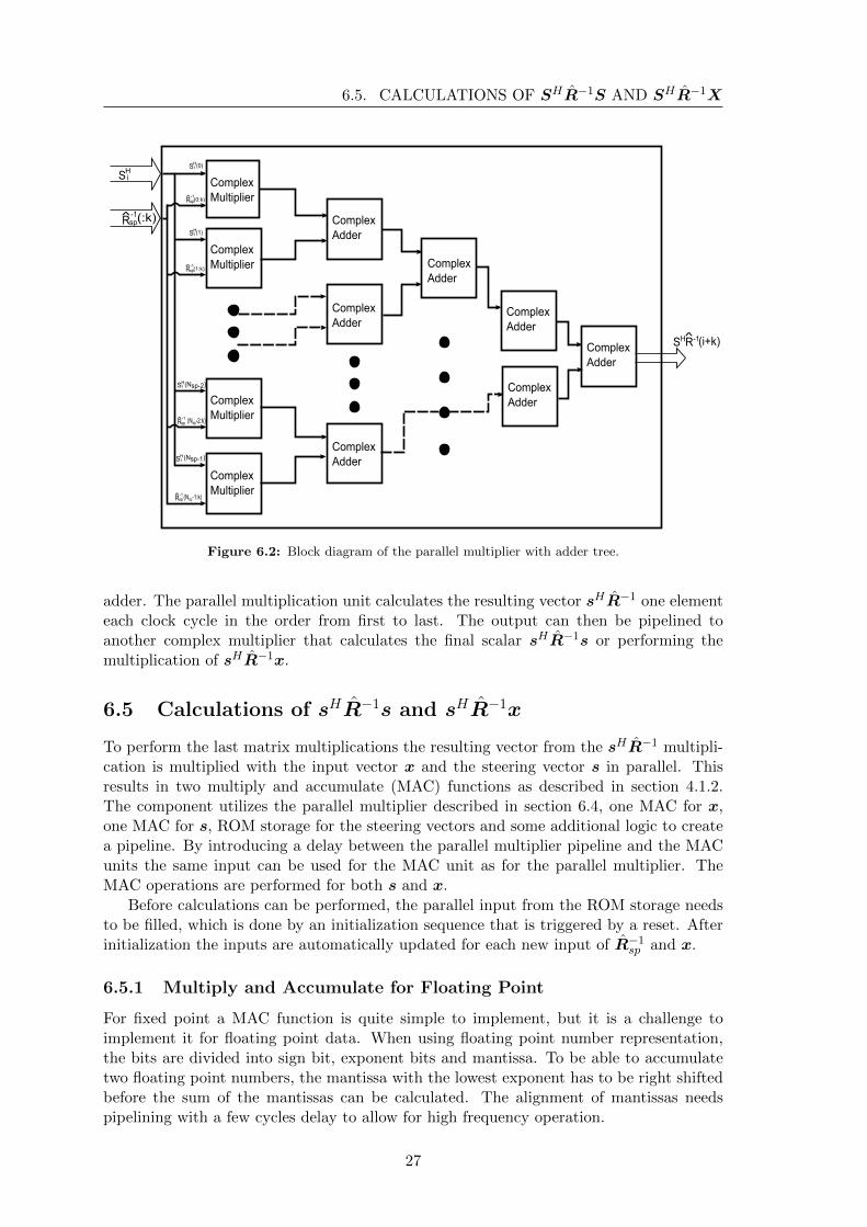
The parallel multiplier is designed to solve the matrix multiplication between sH and R−1,although not the entire operation in parallel but column by column of R−1. It utilizes thecomplex multiplier described in section 6.3 along with complex adders. Nsp multipliers areimplemented in parallel and use an adder tree structure after the multipliers to calculatethe sum of the multiplier products. This is illustrated in Figure 6.2. The resulting outputis an element in the vector sHR−1. Every iteration, k is increased until k = Nsp. The
parameter k is controlling what column of Rsp the parallel multiplier is processing. Whenthe last column is done, it starts over with k = 0 and i is incremented to use the next partof the steering vector.
The number of adders used to sum the output from the multipliers adds up to Nsp− 1and the latency through the adder tree, which results from registers between inputs andoutputs of the adders, can be calculated by log2(Nsp) multiplied with the latency of an
26
6.5. CALCULATIONS OF SHR−1S AND SHR−1X
ComplexMultiplier
ComplexMultiplier
ComplexMultiplier
ComplexMultiplier
SHi
^Rsp-1
SHi
SHi
SHi
SHi
(0)
(1)
(Nsp-2)
(Nsp-1)
^Rsp-1
^Rsp-1
^Rsp-1
^Rsp-1
ComplexAdder
ComplexAdder
ComplexAdder
ComplexAdder
ComplexAdder
ComplexAdder
ComplexAdder
SHR-1^ (i+k)
(:k)
(0:k)
(1:k)
(Nsp-2:k)
(Nsp-1:k)
Figure 6.2: Block diagram of the parallel multiplier with adder tree.
adder. The parallel multiplication unit calculates the resulting vector sHR−1 one elementeach clock cycle in the order from first to last. The output can then be pipelined toanother complex multiplier that calculates the final scalar sHR−1s or performing themultiplication of sHR−1x.
6.5 Calculations of sHR−1s and sHR−1x
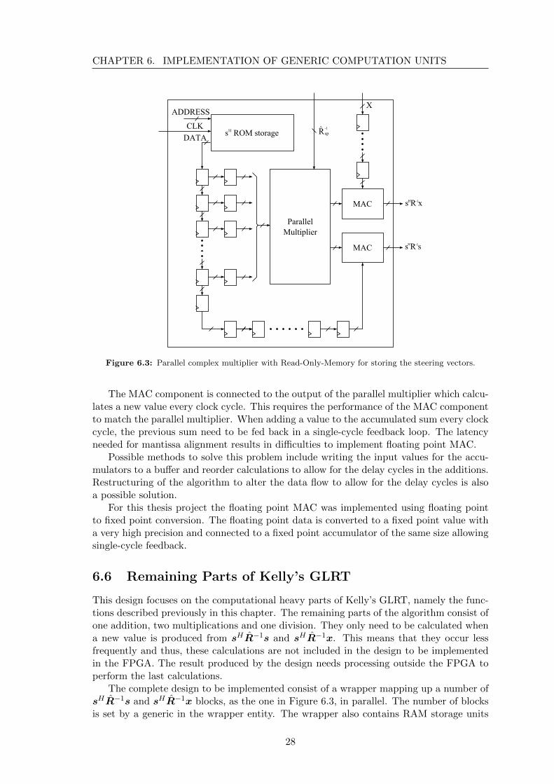
To perform the last matrix multiplications the resulting vector from the sHR−1 multipli-cation is multiplied with the input vector x and the steering vector s in parallel. Thisresults in two multiply and accumulate (MAC) functions as described in section 4.1.2.The component utilizes the parallel multiplier described in section 6.4, one MAC for x,one MAC for s, ROM storage for the steering vectors and some additional logic to createa pipeline. By introducing a delay between the parallel multiplier pipeline and the MACunits the same input can be used for the MAC unit as for the parallel multiplier. TheMAC operations are performed for both s and x.
Before calculations can be performed, the parallel input from the ROM storage needsto be filled, which is done by an initialization sequence that is triggered by a reset. Afterinitialization the inputs are automatically updated for each new input of R−1
sp and x.
6.5.1 Multiply and Accumulate for Floating Point
For fixed point a MAC function is quite simple to implement, but it is a challenge toimplement it for floating point data. When using floating point number representation,the bits are divided into sign bit, exponent bits and mantissa. To be able to accumulatetwo floating point numbers, the mantissa with the lowest exponent has to be right shiftedbefore the sum of the mantissas can be calculated. The alignment of mantissas needspipelining with a few cycles delay to allow for high frequency operation.
27
CHAPTER 6. IMPLEMENTATION OF GENERIC COMPUTATION UNITS
DATAROM storagesH
CLK
ADDRESS
ParallelMultiplier
MAC
Rsp^ -1
MAC
X
s R sH -1
s R xH -1
Figure 6.3: Parallel complex multiplier with Read-Only-Memory for storing the steering vectors.
The MAC component is connected to the output of the parallel multiplier which calcu-lates a new value every clock cycle. This requires the performance of the MAC componentto match the parallel multiplier. When adding a value to the accumulated sum every clockcycle, the previous sum need to be fed back in a single-cycle feedback loop. The latencyneeded for mantissa alignment results in difficulties to implement floating point MAC.
Possible methods to solve this problem include writing the input values for the accu-mulators to a buffer and reorder calculations to allow for the delay cycles in the additions.Restructuring of the algorithm to alter the data flow to allow for the delay cycles is alsoa possible solution.
For this thesis project the floating point MAC was implemented using floating pointto fixed point conversion. The floating point data is converted to a fixed point value witha very high precision and connected to a fixed point accumulator of the same size allowingsingle-cycle feedback.
6.6 Remaining Parts of Kelly’s GLRT
This design focuses on the computational heavy parts of Kelly’s GLRT, namely the func-tions described previously in this chapter. The remaining parts of the algorithm consist ofone addition, two multiplications and one division. They only need to be calculated whena new value is produced from sHR−1s and sHR−1x. This means that they occur lessfrequently and thus, these calculations are not included in the design to be implementedin the FPGA. The result produced by the design needs processing outside the FPGA toperform the last calculations.
The complete design to be implemented consist of a wrapper mapping up a number ofsHR−1s and sHR−1x blocks, as the one in Figure 6.3, in parallel. The number of blocksis set by a generic in the wrapper entity. The wrapper also contains RAM storage units
28
6.6. REMAINING PARTS OF KELLY’S GLRT
for R−1sp and x, described further in section 6.7.
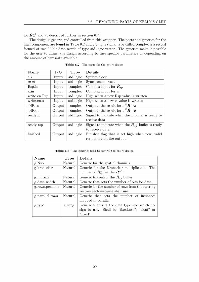
The design is generic and controlled from this wrapper. The ports and generics for thefinal component are found in Table 6.2 and 6.3. The signal type called complex is a recordformed of two 32-bit data words of type std logic vector. The generics make it possiblefor the user to adjust the design according to case specific parameters or depending onthe amount of hardware available.
Table 6.2: The ports for the entire design.
Name I/O Type Details
clk Input std logic System clock
reset Input std logic Synchronous reset
Rsp in Input complex Complex input for Rsp
x in Input complex Complex input for x
write en Rsp Input std logic High when a new Rsp value is written
write en x Input std logic High when a new x value is written
sHRs s Output complex Outputs the result for sHR−1s
sHRx s Output complex Outputs the result for sHR−1x
ready x Output std logic Signal to indicate when the x buffer is ready toreceive data
ready rsp Output std logic Signal to indicate when the R−1sp buffer is ready
to receive data
finished Output std logic Finished flag that is set high when new, validresults are on the outputs
Table 6.3: The generics used to control the entire design.
Name Type Details
g Nsp Natural Generic for the spatial channels
g kronecker Natural Generic for the Kronecker multiplicand. Thenumber of R−1
sp in the R−1.
g fifo size Natural Generic to control the Rsp buffer
g data width Natutal Generic that sets the number of bits for data
g rows per unit Natural Generic for the number of rows from the steeringvectors each instance shall use
g parallel rows Natural Generic that sets the number of instancesmapped in parallel
g type String Generic that sets the data type and which de-sign to use. Shall be “fixed ntd”, “float” or“fixed”
29
CHAPTER 6. IMPLEMENTATION OF GENERIC COMPUTATION UNITS
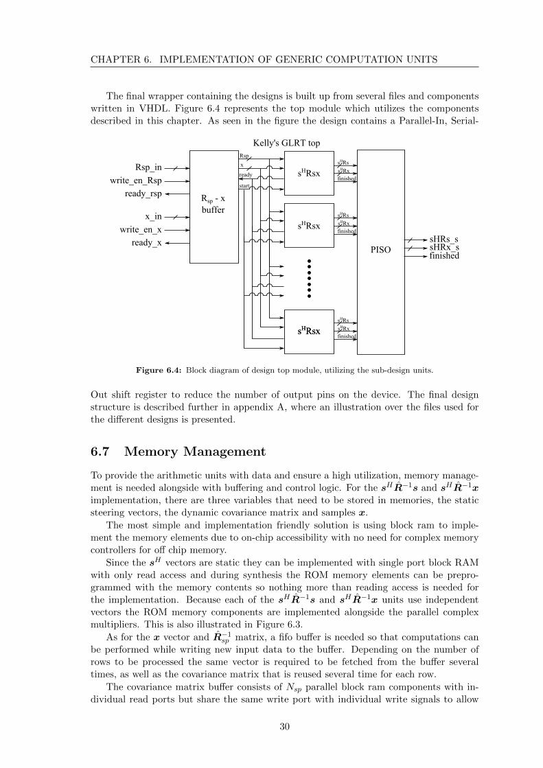
The final wrapper containing the designs is built up from several files and componentswritten in VHDL. Figure 6.4 represents the top module which utilizes the componentsdescribed in this chapter. As seen in the figure the design contains a Parallel-In, Serial-
Rsp - x buffer
sHRsx
sHRsx
sHRsxsHRsx
Rsp_in
write_en_Rsp
ready_rsp
x_in
write_en_x
ready_x
Rsp
x
ready
start
sHRs
sHRxfinished
sHRs
sHRxfinished
sHRs
sHRxfinished
sHRs_ssHRx_sfinished
PISO
Kelly's GLRT top
Figure 6.4: Block diagram of design top module, utilizing the sub-design units.
Out shift register to reduce the number of output pins on the device. The final designstructure is described further in appendix A, where an illustration over the files used forthe different designs is presented.
6.7 Memory Management
To provide the arithmetic units with data and ensure a high utilization, memory manage-ment is needed alongside with buffering and control logic. For the sHR−1s and sHR−1ximplementation, there are three variables that need to be stored in memories, the staticsteering vectors, the dynamic covariance matrix and samples x.
The most simple and implementation friendly solution is using block ram to imple-ment the memory elements due to on-chip accessibility with no need for complex memorycontrollers for off chip memory.
Since the sH vectors are static they can be implemented with single port block RAMwith only read access and during synthesis the ROM memory elements can be prepro-grammed with the memory contents so nothing more than reading access is needed forthe implementation. Because each of the sHR−1s and sHR−1x units use independentvectors the ROM memory components are implemented alongside the parallel complexmultipliers. This is also illustrated in Figure 6.3.
As for the x vector and R−1sp matrix, a fifo buffer is needed so that computations can
be performed while writing new input data to the buffer. Depending on the number ofrows to be processed the same vector is required to be fetched from the buffer severaltimes, as well as the covariance matrix that is reused several time for each row.
The covariance matrix buffer consists of Nsp parallel block ram components with in-dividual read ports but share the same write port with individual write signals to allow
30
6.7. MEMORY MANAGEMENT
RAM
RAM
RAM
RAM
Wri
te E
nabl
e
Wri
te A
ddr
Dat
a
Data
Data
Data
Data
Rea
d A
ddr
Figure 6.5: Parallel block rams with shared addresses, input data and parallel output.
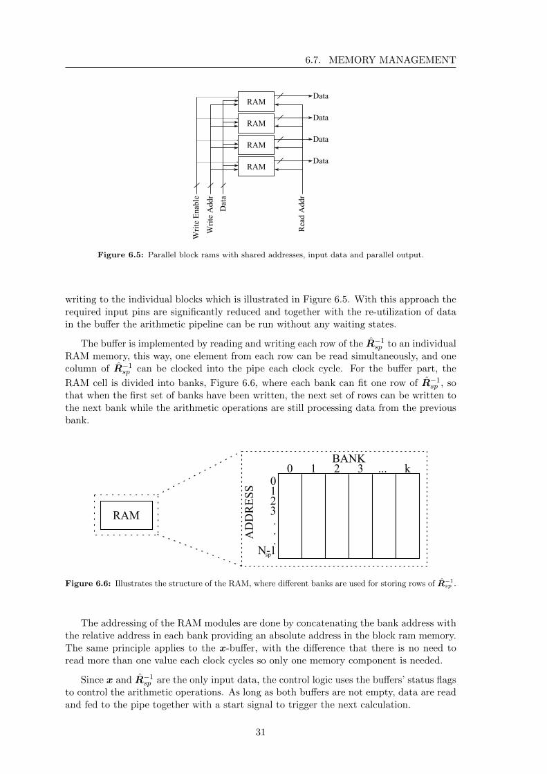
writing to the individual blocks which is illustrated in Figure 6.5. With this approach therequired input pins are significantly reduced and together with the re-utilization of datain the buffer the arithmetic pipeline can be run without any waiting states.
The buffer is implemented by reading and writing each row of the R−1sp to an individual
RAM memory, this way, one element from each row can be read simultaneously, and onecolumn of R−1
sp can be clocked into the pipe each clock cycle. For the buffer part, the
RAM cell is divided into banks, Figure 6.6, where each bank can fit one row of R−1sp , so
that when the first set of banks have been written, the next set of rows can be written tothe next bank while the arithmetic operations are still processing data from the previousbank.
RAM
BANK0 1 2 3 ... k
AD
DR
ES
S
0123...
N-1sp
Figure 6.6: Illustrates the structure of the RAM, where different banks are used for storing rows of R−1sp .
The addressing of the RAM modules are done by concatenating the bank address withthe relative address in each bank providing an absolute address in the block ram memory.The same principle applies to the x-buffer, with the difference that there is no need toread more than one value each clock cycles so only one memory component is needed.
Since x and R−1sp are the only input data, the control logic uses the buffers’ status flags
to control the arithmetic operations. As long as both buffers are not empty, data are readand fed to the pipe together with a start signal to trigger the next calculation.
31
CHAPTER 6. IMPLEMENTATION OF GENERIC COMPUTATION UNITS
6.8 Functional Verification using MATLAB and Testbench
All components are tested to verify their functional behaviour. For smaller componentsand functions, simulations in ModelSim are done. For the larger components, such as theparallel multiplier and the final wrapper, a generic testbench was written in VHDL. Thestimuli data is generated by running a matlab script before running the testbench thefirst time. All stimuli data and results are saved in text files and read by the testbench.The testbench feeds the components with stimuli data and checks the result. For a morespecific description of the testbench see appendix B.
32
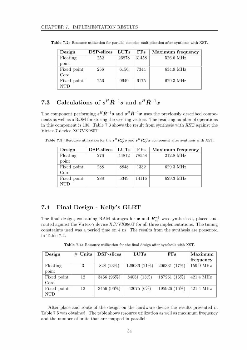
7. Implementation Results
This chapter presents the results from the implementation described in chapter 6. Theresults are basen on Virtex-7 as target hardware using XST as synthesis tool. The completeresults for Virtex-5 and Synplify Pro can be found in appendix C.1 and C.2.
The components without the memory management are not possible to place and routedue to the large amount of I/O pins. Thus, only the result after synthesis is presented forthe smaller components. For the final design the results from both synthesis and placeand route are presented.
Example parameter sizes are used to achieve results that reflect reality. The parameterg Nsp in this example is 16 and the Kronecker parameter is set to 30. The two parametersset the length of vectors s and x to 480 elements and R−1 the size of 480×480. Theseparameters are used to obtain the results presented in this chapter.
Results for single precision floating point and fixed point of 32 bits are presented for allrelevant components designed in this thesis followed by the result from a comparison be-tween Virtex-5 and Virtex-7 as well as XST and Synplify Pro. Finally the result regardingthe scalability of the design is presented.
7.1 Complex Multiplier
The results presented in Table 7.1 is from when synthesizeing the complex multiplieragainst the Xilinx Virtex-7 device XC7VX980T using XST.
Table 7.1: Resource utilization for complex multiplication after synthesis with ISE XST.
Design DSP-slices LUTs FFs Maximum frequency
Floatingpoint
12 1123 1338 526.6 MHz
Fixed pointCore
16 261 365 634.9 MHz
Fixed pointNTD
16 165 323 623.3 MHz
7.2 Parallel Multiplier
The parallel multiplier is Nsp complex multipliers in parallel. Their resulting products isadded up in a tree of adders as described in chapter 6.4. Using the example parametersthe design required 16 complex multipliers to perform the calculations as intended. Whensynthesizeing the parallel complex multiplier against the Virtex-7 device XC7VX980Tusing XST the result presented in Table 7.2 was gained.
33
CHAPTER 7. IMPLEMENTATION RESULTS
Table 7.2: Resource utilization for parallel complex multiplication after synthesis with XST.
Design DSP-slices LUTs FFs Maximum frequency
Floatingpoint
252 26878 31458 526.6 MHz
Fixed pointCore
256 6156 7344 634.9 MHz
Fixed pointNTD
256 9649 6175 629.3 MHz
7.3 Calculations of sHR−1s and sHR−1x
The component performing sHR−1s and sHR−1x uses the previously described compo-nents as well as a ROM for storing the steering vectors. The resulting number of operationsin this component is 138. Table 7.3 shows the result from synthesis with XST against theVirtex-7 device XC7VX980T.
Table 7.3: Resource utilization for the sHR−1sp s and sHR−1
sp x component after synthesis with XST.
Design DSP-slices LUTs FFs Maximum frequency
Floatingpoint
276 44812 78558 212.8 MHz
Fixed pointCore
288 8848 1332 629.3 MHz
Fixed pointNTD
288 5349 14116 629.3 MHz
7.4 Final Design - Kelly’s GLRT
The final design, containing RAM storages for x and R−1sp was synthesised, placed and
routed against the Virtex-7 device XC7VX980T for all three implementations. The timingconstraints used was a period time on 4 ns. The results from the synthesis are presentedin Table 7.4.
Table 7.4: Resource utilization for the final design after synthesis with XST.
Design # Units DSP-slices LUTs FFs Maximumfrequency
Floatingpoint
3 828 (23%) 129036 (21%) 206331 (17%) 159.9 MHz
Fixed pointCore
12 3456 (96%) 84051 (13%) 187261 (15%) 421.4 MHz
Fixed pointNTD
12 3456 (96%) 42075 (6%) 195926 (16%) 421.4 MHz
After place and route of the design on the hardware device the results presented inTable 7.5 was obtained. The table shows resource utilization as well as maximum frequencyand the number of units that are mapped in parallel.
34
7.5. SYSTEM PERFORMANCE
Table 7.5: Resource utilization for the final design after place and route.
Design # Units DSP-slices LUTs FFs Maximumfrequency
Floatingpoint
3 828 (23%) 117011 (19%) 167219 (13%) 140.1 MHz
Fixed pointCore
12 3456 (96%) 79220 (12%) 162416 (13%) 168.9 MHz
Fixed pointNTD
12 3456 (96%) 60777 (9%) 195798 (15%) 189.3 MHz
7.5 System Performance
The following section present the result for the entire design according to performancemeasured in the amount of operations performed by one device with the specific designimplemented. Table 7.6 displays the results consisting on the system frequency, numberof sHR−1s and sHR−1x units mapped in parallel and the total amount of operations forthe implementation. As mentioned in section 7.3, the number of operations per unit is138.
Table 7.7 presents the performance in a more general way. The power consumption forthe design is presented and the performance is measured in operations per second (OPS)for either floating point (FL) or fixed point (FI). The OPS gained for the design is thendivided with the power consumed by the device to give a general result that can easily becompared to other implementations.
Table 7.6: Performance of final system implemented on Virtex-7.
Design Maximumfrequency
# Units Tot. Operations
Floatingpoint
140.1 MHz 3 58 GFLOPS
Fixed pointCore
168.9 MHz 12 280 GFIOPS
Fixed pointNTD
189.3 MHz 12 313 GFIOPS
Table 7.7: Power efficiency of final system implemented on Virtex-7.
Design Power Consumption Performance Ops/W
Floating point 2.500 W 58 GFLOPS 23.2 GFLOPS/W
Fixed point Core 8.171 W 280 GFIOPS 34.3 GFIOPS/W
Fixed point NTD 7.981 W 313 GFIOPS 39.3 GFIOPS/W
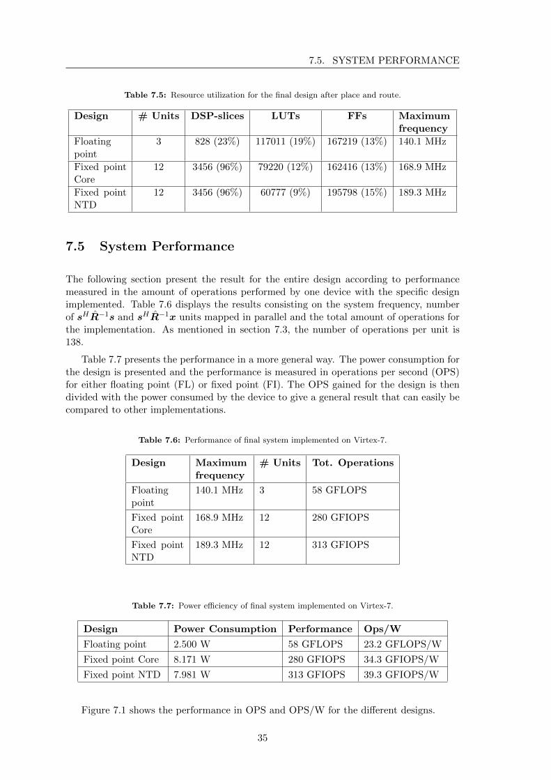
Figure 7.1 shows the performance in OPS and OPS/W for the different designs.
35
CHAPTER 7. IMPLEMENTATION RESULTS
Fixed NTD Fixed Core Floating point0
100
200
300
313
280
58
39.3
34.3
23.2
Op
erat
ion
s
GOPS GOPS/W
Figure 7.1: System perfomance for the three designs presented in GOPS and GOPS/W.
7.6 Synthesis tools
The final design is built from the components described in sections 7.1, 7.2 and 7.3. Whenusing Synplify Pro as the tool for synthesis for those components and comparing the resultto the one after synthesis with XST indicates an overall higher performance using XST.The resource utilization did not differ too much, but the estimated maximum frequencydiffered according to Table 7.8.
Table 7.8: Comparison of XST and Synplify Pro for the base components of the design.
Frequency XST Frequency Synplify Pro
Complex Multiplier Floating Point 526.6 MHz 507.5 MHz
Complex Multiplier Fixed Point Core 634.9 MHz 529.4 MHz
Complex Multiplier Fixed Point NTD 623.3 MHz 250.3 MHz
Parallel Multiplier Floating Point 526.6 MHz 507.5 MHz
Parallel Multiplier Fixed Point Core 634.9 MHz 381.1 MHz
Parallel Multiplier Fixed Point NTD 629.3 MHz 250.3 MHz
The result presented in the Table is from when synthesizing against the Virtex-7 deviceXC7VX980T. As seen in the Table, the biggest difference is when using the NTD designfor fixed point implementation.
7.7 Scalability
The design is intended to be scalable when considering migrating from one technologygeneration to the next. The design is generic and scalable so that the same design isfunctional for different sizes of the data parameters specific for the application. To changethe data parameters, the generics of the design are used.
When migrating from one technology to the next it is possible to map more parallelsHR−1s and sHR−1x modules according to the available resources. The NTD designis completely scalable between different devices. However, the design using IP cores isnot scalable between different generations. In this thesis the designs was implemented
36
7.8. FLOATING POINT IMPLEMENTATION DESIGNED FOR SPECIFICHARDWARE
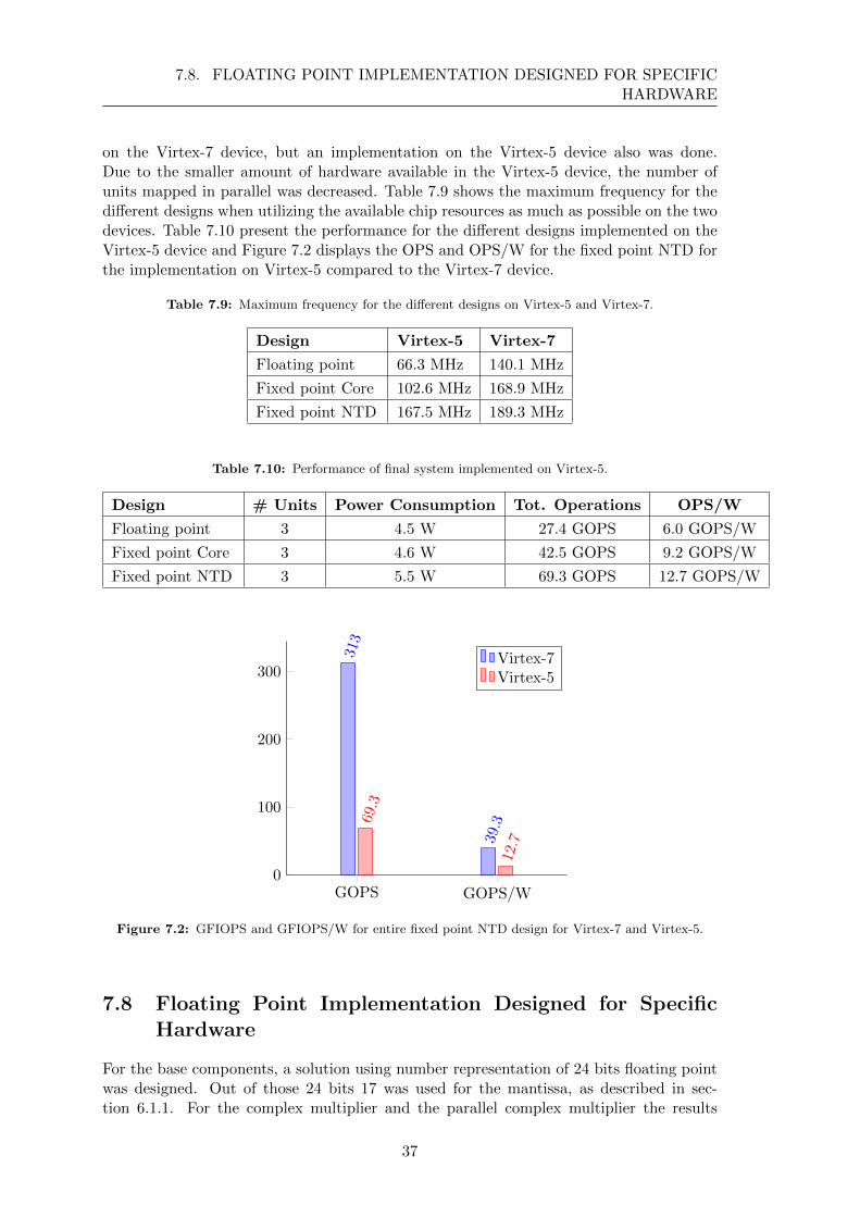
on the Virtex-7 device, but an implementation on the Virtex-5 device also was done.Due to the smaller amount of hardware available in the Virtex-5 device, the number ofunits mapped in parallel was decreased. Table 7.9 shows the maximum frequency for thedifferent designs when utilizing the available chip resources as much as possible on the twodevices. Table 7.10 present the performance for the different designs implemented on theVirtex-5 device and Figure 7.2 displays the OPS and OPS/W for the fixed point NTD forthe implementation on Virtex-5 compared to the Virtex-7 device.
Table 7.9: Maximum frequency for the different designs on Virtex-5 and Virtex-7.
Design Virtex-5 Virtex-7
Floating point 66.3 MHz 140.1 MHz
Fixed point Core 102.6 MHz 168.9 MHz
Fixed point NTD 167.5 MHz 189.3 MHz
Table 7.10: Performance of final system implemented on Virtex-5.
Design # Units Power Consumption Tot. Operations OPS/W
Floating point 3 4.5 W 27.4 GOPS 6.0 GOPS/W
Fixed point Core 3 4.6 W 42.5 GOPS 9.2 GOPS/W
Fixed point NTD 3 5.5 W 69.3 GOPS 12.7 GOPS/W
GOPS GOPS/W0
100
200
300
313
39.369.3
12.7
Virtex-7Virtex-5
Figure 7.2: GFIOPS and GFIOPS/W for entire fixed point NTD design for Virtex-7 and Virtex-5.
7.8 Floating Point Implementation Designed for SpecificHardware
For the base components, a solution using number representation of 24 bits floating pointwas designed. Out of those 24 bits 17 was used for the mantissa, as described in sec-tion 6.1.1. For the complex multiplier and the parallel complex multiplier the results
37
CHAPTER 7. IMPLEMENTATION RESULTS
Table 7.11: Synthesis results for complex multiplier and parallel multiplier using 24 bits floating pointnumber representation.
Design DSP-slices LUTs FFs Maximum frequency
Complex Multiplier 4 1127 1240 561.0 MHz
Parallel Complex Multiplier 64 28442 31840 561.0 MHz
presented in Table 7.11 was obtained. The same example parameters were used and theVirtex-7 device was the target hardware platform. XST was used for synthesis.
38
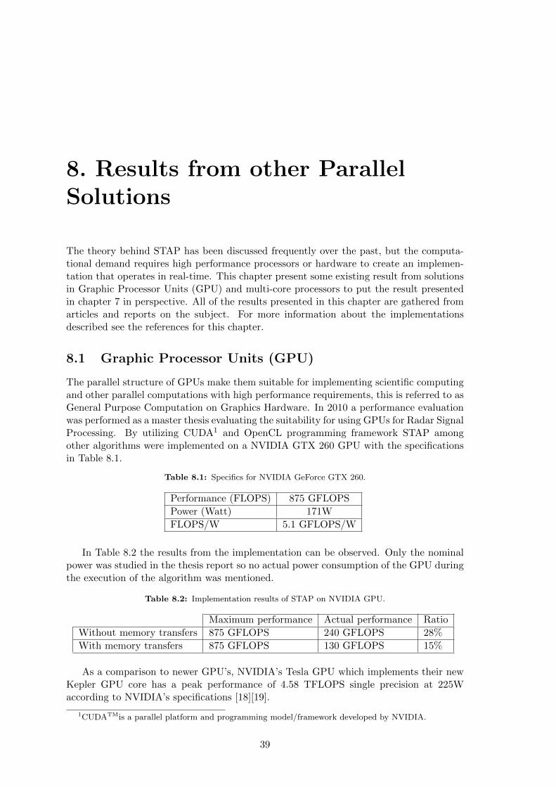
8. Results from other ParallelSolutions
The theory behind STAP has been discussed frequently over the past, but the computa-tional demand requires high performance processors or hardware to create an implemen-tation that operates in real-time. This chapter present some existing result from solutionsin Graphic Processor Units (GPU) and multi-core processors to put the result presentedin chapter 7 in perspective. All of the results presented in this chapter are gathered fromarticles and reports on the subject. For more information about the implementationsdescribed see the references for this chapter.
8.1 Graphic Processor Units (GPU)
The parallel structure of GPUs make them suitable for implementing scientific computingand other parallel computations with high performance requirements, this is referred to asGeneral Purpose Computation on Graphics Hardware. In 2010 a performance evaluationwas performed as a master thesis evaluating the suitability for using GPUs for Radar SignalProcessing. By utilizing CUDA1 and OpenCL programming framework STAP amongother algorithms were implemented on a NVIDIA GTX 260 GPU with the specificationsin Table 8.1.
Table 8.1: Specifics for NVIDIA GeForce GTX 260.
Performance (FLOPS) 875 GFLOPS
Power (Watt) 171W
FLOPS/W 5.1 GFLOPS/W
In Table 8.2 the results from the implementation can be observed. Only the nominalpower was studied in the thesis report so no actual power consumption of the GPU duringthe execution of the algorithm was mentioned.
Table 8.2: Implementation results of STAP on NVIDIA GPU.
Maximum performance Actual performance Ratio
Without memory transfers 875 GFLOPS 240 GFLOPS 28%
With memory transfers 875 GFLOPS 130 GFLOPS 15%
As a comparison to newer GPU’s, NVIDIA’s Tesla GPU which implements their newKepler GPU core has a peak performance of 4.58 TFLOPS single precision at 225Waccording to NVIDIA’s specifications [18][19].
1CUDATMis a parallel platform and programming model/framework developed by NVIDIA.
39
CHAPTER 8. RESULTS FROM OTHER PARALLEL SOLUTIONS
8.2 Multi-core Processors
The company BittWare has a multi-core co-processor for FPGAs in their product rangethat in their case work together with an Altera Stratix FPGA. The co-processor is namedAnemone and creates a hybrid solution for floating point operations. Anemone is a lowpower multi-core processor consisting of 16 floating point cores and is scalable for up toa maximum of 4096 cores providing a peak of 4.9 TFLOPS [20]. According to BittWarethe Anemone is able to provide 19.2 GFLOPS/W in computational performance.
The multi-core processor has been used for implementation of a matrix multiplicationalgorithm called xGEMM, which suggests that the processor has been capable of up to90% of the theoretical performance peak for that specific algorithm using 16 cores [21].
40
9. Discussion
The intention of this chapter is to discuss the results and the advantages and disadvantagesof the different designs compared to one another. The focus is on what have impact onthe results, why and how the bottlenecks might be solved. The hardware, tools andperformance are discussed and analysed. In addition to discussing the design this chapteralso intends to analyse and reason about the suitability for implementing STAP on anFPGA in the near future.
9.1 Hardware platform
The target platform in this thesis work is a Xilinx Virtex-7 device and it is of importancethat this is not the only suitable platform on the market. There are a number of vendorson the market and the designs of the different FPGAs are not identical. When the deviceStratix V from Altera was studied it was found that the DSP blocks used in this device areslightly different. The datasheet for the device says that the device supports up to 3,92618×18 or 1,963 27×27 multipliers [22]. Even though this thesis work focused on hardwareplatforms from Xilinx, it might be interesting to investigate other vendors further to reachthe best result.
Focusing on the Xilinx Virtex-7 and Virtex-5 devices, one aspect is that the sliceschange over time. Just by studying the two devices in this thesis work some differencesare found. It is therefore likely that the development of future generations include moreDSP slices and might contain even larger, more advanced DSP slices, with a possibility ofimproving the design even further.
9.2 Tools
During this thesis work the impact of the tools have been obvious, especially for thepipelined, non-technology dependent solution. In Table 7.8 one could clearly see resultsthat differed depending on whether XST or Synplify Pro was used as synthesis tool.The designer needs knowledge about the tool to understand the result and to be able tooptimize the design. The pipelined NTD design presented in this thesis is, as mentioned,non-technology dependent but still designed to be implemented as a tailored solution forthis kind of DSP slice. The problem when using Synplify Pro for synthesis is that thetool is too general and can not handle the internal register in the DSP slices in the mostefficient way. For this design solution to work and be fast enough, the internal registersin the DSP slices should be used for creating parts of the pipeline. Synplify Pro does notuse those registers as intended, resulting in a very slow design. XST is a Xilinx tool forsynthesis, and more aware of the DSP slice registers and how to pipeline those for a fasterdesign.
41
CHAPTER 9. DISCUSSION
Recently Xilinx provided the designers with a design suite called Vivado [23]. Vivadois a new design environment provided to accelerate designs on the Xilinx 7 series. If thisdesign suite was used instead of ISE it could, according to the Vivado overview, improvefrequency, power consumption, build-time and other parameters even further. Vivado wasnot in focus in this thesis work, but some minor tests were performed for the final design.Using Vivado, it was possible to implement the floating point design while utilizing theresources in the FPGA to a higher extent compared to when using ISE. However, the resultfrom the tests with Vivado are not presented in this thesis due to the fact that the resultswere not verified. This had to do with lack of time and experience regarding the tool. Butthe tests did imply that Vivado might be of interest for implementing the floating pointdesign and could possibly achieve better results for the design, both regarding speed andnumber of units possible to implement.
9.3 Number Representation
During the first phases of the design, results showed that the components for floatingpoint could compete with the ones for fixed point. The estimated maximum frequencywas slightly lower for the floating point design. However, the floating point design utilizessignificantly more logic. During the development of the design it was not clear if it wasthe logic or the DSP slices that would be the limiting factor. In the final synthesis resultit was found that for the floating point implementation it was in fact also the DSP slicesthat was the limiting factor. The intention was to use as much of the FPGA as possibleand for the fixed point designs, with less logic, that logic is not used for anything else.It might be possible to implement other parts of the algorithm or the signal processingchain by using this logic, giving these solutions an even greater advantage compared tothe floating point implementation.
One problem with the floating point design occurred when including the MAC func-tions. As described in section 6.5.1, the latency of the accumulation results in a ratherslow solution. To solve this, the data is transformed to fixed point before performing theaccumulation. The transformation is not optimal and might lead to loss of precision. Itis possible to minimize the loss of precision, but it would most definitely require moreresources. Also, this implementation requires additional hardware that could be used forother parts of the algorithm.
Finally, when trying to utilize the Virtex-7 resources as much as possible, ISE couldnot implement the floating point design. Hence, we only got synthesis results for thatimplementation. However, the design was possible to implement on the Virtex-5 devicewith high utilization, but the smaller FPGA resulted in fewer parallel modules. Using thesame, lower number of modules in the Virtex-7 device implementation succeeded, utilizingthe device to a smaller extent than intended. The reason for the problems with the Virtex-7 device were not solved, but it probably has to do with different optimization algorithmsused depending on the device. When using the new tool Vivado, the synhtesized netlistfor the high utilization could be implemented on the Virtex-7 device.
The use of floating point number representation is quite new for the vendors and itis not unlikely to believe that support will increase and as an example a better solutionfor floating point MAC will exist in a near future. It might also be possible to design thesolution in a different way so that a single-cycle feedback loop no longer is needed.
When using only 24 bits for floating point number representation the solution only needone DSP slice to perform the multiplication. Compared to the single precision numberrepresentation, this resulted in 4 DSP slices instead of 12 for a complex multiplier. A
42
9.4. PERFORMANCE
design using fewer bits for number representation should also result in fewer wires to route.However, this solution utilizes almost the same amount of logic so it would require moreoptimization before the benefits of the reduced number of DSP slices can be used. If thesystem can tolerate a small loss of precision and dynamic range, it would be interestingto optimize this design and obtain a final result in terms of power consumption andperformance.
9.4 Performance
Evaluating the design results from this thesis with the other parallel solutions and com-paring both peak performance and power efficiency there is no obvious winner in thecompetition. The FPGA approach is able to utilize logic efficiently and also provides adense operations/power ratio, this is also true for the GPU. However, when only utiliz-ing the approximately 18-25% of the peak performance it is not known what the powerconsumption at that point is, hence, the actual operations/power ratio is not known. Alimiting factor for the FPGA approach considering performance is the slow clock frequency,this is however due to a couple of bottlenecks in the design which should be possible toimprove for increased performance.
In comparison to the multi-core Anemone processor, it seems that a multi-core pro-cessor approach could be beneficial for floating point operations. The performance of upto 90% of the theoretical maximum for matrix and vector operations indicates that themulti-core processor architecture is suitable for matrix type computation. The Anemoneis a co-processor for FPGAs, a hybrid solution that is designed to use the FPGA for someparts of the signal processing but perform calculations that benefit more when run on theco-processor on the Anemone. This implies that if more work in these two areas are made,both the multi-core solution as well as the FPGA approach might have the capacity ofbeing more energy efficient and have an overall higher performance.
The usual way of limiting power consumption in CPU and GPU architectures is doneby switching off unused sections of the chips while computational load is low, but this cannot be performed perfectly, and because of this, the operations/power ratio is probablysignificantly lower than the ratio of peak performance over peak power since the utilizationof the STAP algorithm on CUDA cores reached 25% at most.
To be able to determine which solution would be most energy efficient, an analysis isneeded to determine power consumption and not only performance evaluation for imple-mentation of the STAP algorithm. More work in both the FPGA design as well as forthe GPU and multi-core processor solutions is required to be able to make more relevantconclusions.
9.5 Implementation of STAP on an FPGA
Results from the fixed point implementation in this thesis implies that FPGA’s are suitablefor this type of complex multiplications and parallelism. The limiting factor is not theoperations to be performed, but more the routing and transfer of data to and from thememory blocks. It is possible that a design with better routing would lead to a moreenergy efficient design. The design in this thesis work would require a huge amount ofFPGAs to implement a complete STAP system of this magnitude and the intention is touse this in a airborne radar with a limited space for the hardware.
Computational demands of approximately 100 TOPS would result in over 300 FPGAchips. It would be possible to divide the algorithm and spread it out on a number of
43
CHAPTER 9. DISCUSSION
FPGAs but a number of that size is not appropriate. The power consumption of thissystem is slightly above 2400W which exceeds the theoretical maximum of 400W by far.
9.5.1 Bottlenecks of the Design
One of the major bottlenecks in the design is the memory management and buffering ofdata. Due to large fanout and long paths the path delay limits the switching frequency ofthe design while all components are fast enough for significantly higher clock frequencies.
For the floating point implementation the MAC unit is also a major bottleneck, sincethe multiply and accumulate operation with the accumulated sum in a single-cycle feed-back loop is difficult to implement. This is described previously in section 6.5.1 andsection 9.3.
The bottlenecks in the design should be possible to solve by inserting buffer registers tolimit fanout in conjunction with a MAC solution that is pipelined even further. Anotherpossible solution would be to re-design the matrix calculations so that MAC operationswith feedback are avoided and can be implemented using multipliers and adders withoutthe feedback.
44
10. Conclusion
This chapter summarizes the conclusions made in this thesis work. The work is dividedin the development of the design, performance and scaling. For specific results from thedesigns, see chapter 7.
10.1 Design and Number Representation
The final design was implemented on a Xilinx Virtex-7 device using ISE. Both the fixedpoint NTD solution as well as the fixed point solution using IP cores was implementedwith as high utilization of the chip as possible. The final floating point design was notpossible to place and route on the Virtex-7 with resource utilization higher than 25%.However, the floating point design was successfully implemented on the Virtex-5 devicewith as high utilization as possible but could not compare to the results for the fixed pointdesigns.
It was found that the support for floating point arithmetics in the tools need furtherdevelopment to be able to provide high performance operations which is required forimplementation of STAP and Kelly’s GLRT.
10.2 Performance and Power Efficiency
The designs for fixed point had a performance in the interval 35-40 GOPS/W while thefloating point implementation resulted in a slightly lower performance. The results arequite positive, but considering the computational demands and limited space for the radarsystem in an airborne platform they are not good enough. To achieve performance of100 TOPS, this design would require over 300 Virtex-7 devices and result in a powerconsumption of over 2400 W. A system like that is not a realistic solution, why bothperformance and power efficiency needs improvement.
Compared to the GPU approach there is no clear benefit of using FPGAs in favor ofGPUs when considering floating point implementation. However, considering the powerefficiency the FPGAs are superior. The Anemone hybrid solution could compete withthe FPGA approach but also requires an FPGA. Due to the lack of available resultsfrom actual STAP implementations, both considering power efficiency and performanceno concrete conclusion can be drawn.
10.3 Scaling
The final design uses generics to control sizes of memory blocks, input vectors and numberof multipliers in parallel. This makes it possible to adjust the design for a specific caseand making it suitable for different sizes and parameters.
45

CHAPTER 10. CONCLUSION
Due to the generic design, it is possible to change a few generics when a new, largerFPGA is on the market. Instead of a large number of FPGAs working together, thecalculations can be divided on fewer devices of the new FPGA generation where onedevice handles more units in parallel and reducing the total number of FPGAs.
46
11. Future Work
All base components were designed to have a maximum frequency that are as high aspossible. When inserting the RAMs for storing R−1
sp and x, the estimated maximumfrequency decreased significantly. Therefore, one continuation of this work could be toincrease performance by inserting buffer registers to decrease the fan out from the RAMs.This would create a pipelined structure between the RAMs and the components performingthe calculations and probably remove the largest bottleneck of this design.
A recommendation after this thesis work is to implement a floating point library insteadof using the generated IP cores. This would remove some of the technology dependence.Also, it would give the designer the possibility to remove parts that are included in thecores, like different rounding choices not considered in this design. It should not be thathard to implement this library when having some knowledge of the floating point struc-ture. The floating point library would also simplify the design into an even more genericdesign, where a generic easier could set the data type and not requiring different designsdepending on the number representation used. With this thesis in mind it is also likelythat the designer will gain more control over the synthesis and tools performing the syn-thesis when avoiding the core components, especially for the floating point design. Whenrunning the synthesis and place and route, the designs using core components took signif-icantly longer time compared to the pipelined design. The problem with not being able toimplement a similar design for floating point in an efficient way could maybe be solved bythis floating point library. Also, to increase the possibilities of a successful floating pointimplementation even more, a suggestion is that the designer becomes more familiar withthe new tool Vivado. This is simply because the minor tests performed during this thesiswork indicated that Vivado could result in a better floating point implementation.
It could also be of interest to investigate other vendors further. It is a possibility thatthe DSP slices used in other vendors devices might suit this design so that more modulesin parallel can be mapped in a single FPGA. Other vendors also claim their support forfloating point implementations is very good compared to their competitors, and this couldboost the floating point design discussed in this thesis work.
Finally, other parallel solutions should be investigated further. Information and resultfor this kind of implementation is hard to find and to make a fair comparison, moreknowledge is needed. One suggestion for a future thesis work could focus on implementingthe same algorithm on a GPU or multi-core processor and compare the results to the onesachieved in this thesis work for a more genuine evaluation.
47

CHAPTER 11. FUTURE WORK
48
Bibliography
[1] M. Richards, Fundamentals of Radar Signal Processing. McGraw-Hill Electronic En-gineering Series, McGraw-Hill, 2005.
[2] M. Skolnik, Introduction to radar systems. McGraw-Hill, 1962.
[3] A. Ahlander, H. Forsberg, M. Jonsson, and B. Svensson, “Radar signal processingusing pipelined optical hypercube interconnects,” tech. rep., Department of Com-puter Engineering, Chalmers University of Technology, Sweden and Computer andElectrical Engineering, Halmstad University, Sweden and Radar Division, EricssonMicrowave Systems AB, Molndal, Sweden, 2001.
[4] A. Choudhary, W.-K. Liao, D. Weiner, and P. Varshney, “Design, implementation andevaluation of parallel pipelined stap on parallel computers,” in IEEE IPPS/SPDP,vol. 36, pp. 528–548, April 2000.
[5] J. Toomay and P. Hannen, Radar principles for the non-specialist. SciTech radar anddefense series, SciTech Pub., 2004.
[6] S. Montebugnoli, G. Bianchi, A. Cattani, F. Ghelfi, A. Maccaferri, and F. Perini,“The medicina ira-ska engineering group, some notes on beamforming,” 2004. http:
//www.ira.inaf.it/Library/rapp-int-2004/353-04.pdf.
[7] K. Ounissi, “Advanced signal processing techniques for pulse-doppler radar,” Master’sthesis, Chalmers University of Technology, November 2006.
[8] R. Klemm and I. of Electrical Engineers, Principles of Space-Time Adaptive Process-ing. Iee Conference Publication, Institution of Electrical Engineers, 2002.
[9] C. D. Richmond, “The theoretical performance of a class of spacetime adaptive detec-tion and training strategies for airborne radar,” in Conference Record of the Thirty-Second Asilomar Conference on Signals, Systems and Computers, vol. 2, pp. 1327–1331, November 1998.
[10] A. Ahlander and M. Taveniku, “Instruction statistics in array signal processing,”tech. rep., Department of Computer Engineering, Chalmers University of Technology,Sweden and Centre for Computer Systems Architecture, Halmstad University, Swedenand Ericsson Microwave Systems AB, Molndal, Sweden.
[11] A. Devices, “Fixed-point vs floating point digital signal processing.” http://www.
analog.com/en/content/fixed-point vs floating-point dsp/fca.html.
[12] Xilinx, XST Synthesis Overview, 2008. http://www.xilinx.com/itp/xilinx10/isehelp/ise
c using xst for synthesis.htm.
49
BIBLIOGRAPHY
[13] Xilinx, Synthesis and Simulation Design Guide, 13.1 ed., March 2011. http://www.
xilinx.com/support/documentation/sw manuals/xilinx13 1/sim.pdf.
[14] Xilinx, XST User Guide, 10.1 ed., 2008. http://www.xilinx.com/itp/xilinx10/books/
docs/xst/xst.pdf.
[15] Synopsys, Synopsys FPGA Synthesis Reference Manual, September 2011.
[16] Xilinx, Virtex-5 FPGA XtremeDSP Design Considerations User Guide, 3.5 ed., Jan-uary 2012. http://www.xilinx.com/itp/xilinx10/books/docs/xst/xst.pdf.
[17] Altera, Quartus II Handbook Version 12.0, Volume 1: Design and Synthesis, 12.0 ed.,June 2012. http://www.altera.com/literature/hb/qts/qts qii5v1.pdf.
[18] NVIDIA, TESLA K10 GPU Accelerator, 5.0 ed., June 2012. http://www.nvidia.com/
content/PDF/kepler/Tesla K10 BD-06280-001 v05.pdf.
[19] NVIDIA, NVIDIA R© TESLA R© KEPLER GPU Computing Accelerators, 2012. http:
//www.nvidia.com/content/tesla/pdf/NV DS TeslaK Family May 2012 LR.pdf.
[20] BittWare, Anemone104TMCo-Processor for FPGAs, 3.0 ed., October 2012. ftp://ftp.
bittware.com/documents/data sheets/anemone ovrvw.pdf.
[21] Parlant Ltd, Matrix multiplication of the multi-core Anemone processor, April 2011.http://www.paralant.com/docs/Insight-whitepaper-sgemm.pdf.
[22] Altera, Stratix V Device Overview, 3.0 ed., 2012. http://www.altera.com/literature/hb/
stratix-v/stx5 51001.pdf.
[23] Xilinx, Vivado Design Suite, 1.1 ed., 2012. http://www.xilinx.com/support/
documentation/white papers/wp416-Vivado-Design-Suite.pdf.
50
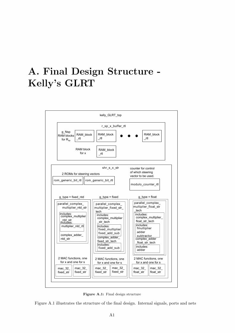
A. Final Design Structure -Kelly’s GLRT
kelly_GLRT_top
r_sp_x_buffer_rtl
shr_s_x_str
RAM_block_rtl
g_NspRAM blocks
for Rsp
RAM blockfor x
modulo_counter_rtlrom_generic_bit_rtl
2 ROMs for steering vectors
counter for controlof which steering vector to be used.
g_type = fixed_ntd g_type = fixed
parallel_complex_multiplier_ntd_str
includes:
includes:multiplier_ntd_rtl
parallel_complex_multiplier_fixed_str_techincludes:
includes:fixed_multiplierfixed_add_sub
includes:fixed_add_sub
g_type = float
parallel_complex_multiplier_float_str_techincludes:
includes:fmultiplieraddersubtractor
includes:adder
2 MAC functions, one for x and one for s
2 MAC functions, one for x and one for s
2 MAC functions, one for x and one for s
complex_multiplier_str_tech
complex_adder_fixed_str_tech
complex_multiplier_ntd_str
complex_adder_ntd_str
complex_multiplier_float_str_tech
complex_adder_float_str_tech
mac_32_fixed_str
mac_32_fixed_str
mac_32_fixed_str
mac_32_fixed_str
mac_32_float_str
mac_32_float_str
RAM_block_rtl
RAM_block_rtl
RAM_block_rtl
rom_generic_bit_rtl
Figure A.1: Final design structure
Figure A.1 illustrates the structure of the final design. Internal signals, ports and nets
A1
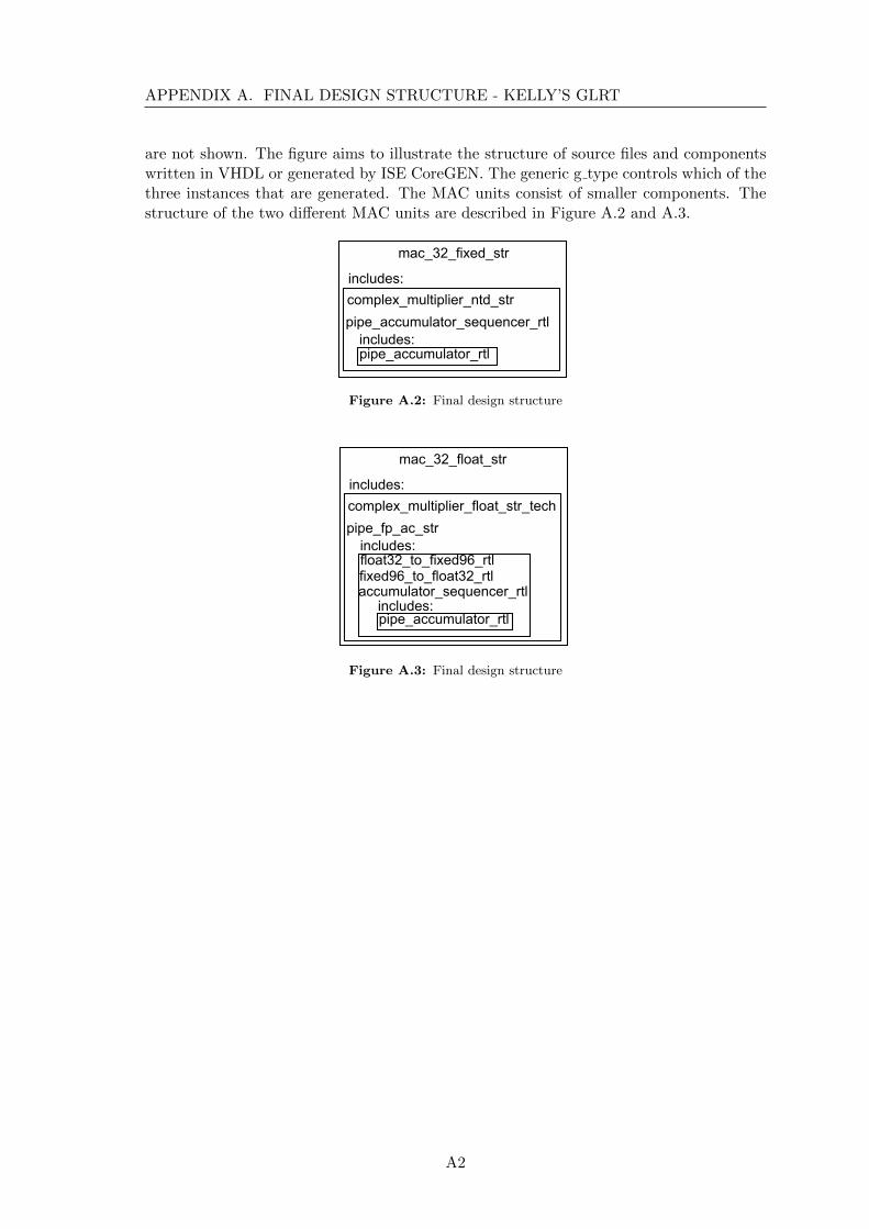
APPENDIX A. FINAL DESIGN STRUCTURE - KELLY’S GLRT
are not shown. The figure aims to illustrate the structure of source files and componentswritten in VHDL or generated by ISE CoreGEN. The generic g type controls which of thethree instances that are generated. The MAC units consist of smaller components. Thestructure of the two different MAC units are described in Figure A.2 and A.3.
complex_multiplier_ntd_str
includes:
pipe_accumulator_sequencer_rtlincludes:pipe_accumulator_rtl
mac_32_fixed_str
Figure A.2: Final design structure
complex_multiplier_float_str_tech
includes:
pipe_fp_ac_strincludes:float32_to_fixed96_rtl
accumulator_sequencer_rtlfixed96_to_float32_rtl
includes:pipe_accumulator_rtl
mac_32_float_str
Figure A.3: Final design structure
A2
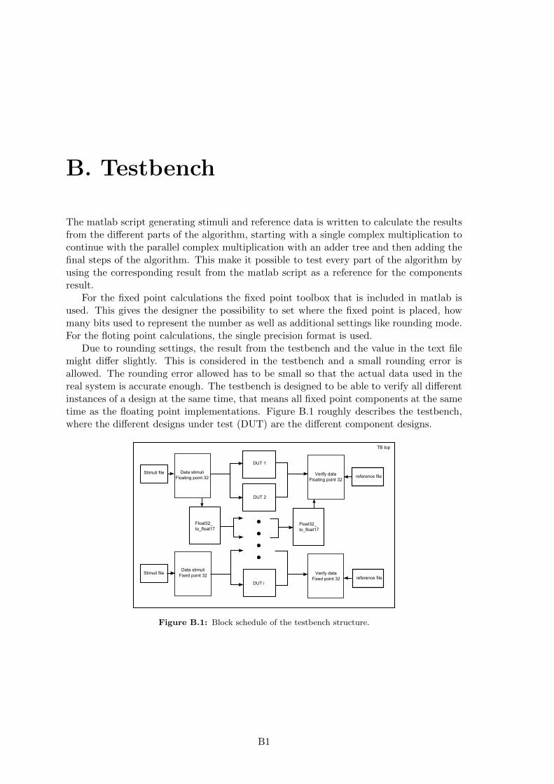
B. Testbench
The matlab script generating stimuli and reference data is written to calculate the resultsfrom the different parts of the algorithm, starting with a single complex multiplication tocontinue with the parallel complex multiplication with an adder tree and then adding thefinal steps of the algorithm. This make it possible to test every part of the algorithm byusing the corresponding result from the matlab script as a reference for the componentsresult.
For the fixed point calculations the fixed point toolbox that is included in matlab isused. This gives the designer the possibility to set where the fixed point is placed, howmany bits used to represent the number as well as additional settings like rounding mode.For the floting point calculations, the single precision format is used.
Due to rounding settings, the result from the testbench and the value in the text filemight differ slightly. This is considered in the testbench and a small rounding error isallowed. The rounding error allowed has to be small so that the actual data used in thereal system is accurate enough. The testbench is designed to be able to verify all differentinstances of a design at the same time, that means all fixed point components at the sametime as the floating point implementations. Figure B.1 roughly describes the testbench,where the different designs under test (DUT) are the different component designs.
TB top
DUT 1
DUT 2
DUT i
Data stimuliFloating point 32
Stimuli file
Float32_to_float17
Data stimuliFixed point 32Stimuli file
Verify dataFloating point 32
reference file
Float32_to_float17
Verify dataFixed point 32 reference file
Figure B.1: Block schedule of the testbench structure.
B1

APPENDIX B. TESTBENCH
B2
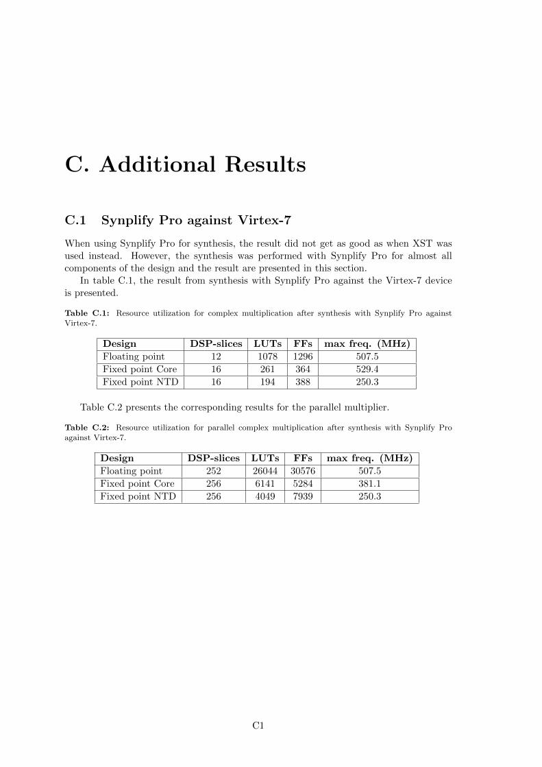
C. Additional Results
C.1 Synplify Pro against Virtex-7
When using Synplify Pro for synthesis, the result did not get as good as when XST wasused instead. However, the synthesis was performed with Synplify Pro for almost allcomponents of the design and the result are presented in this section.
In table C.1, the result from synthesis with Synplify Pro against the Virtex-7 deviceis presented.
Table C.1: Resource utilization for complex multiplication after synthesis with Synplify Pro againstVirtex-7.
Design DSP-slices LUTs FFs max freq. (MHz)
Floating point 12 1078 1296 507.5
Fixed point Core 16 261 364 529.4
Fixed point NTD 16 194 388 250.3
Table C.2 presents the corresponding results for the parallel multiplier.
Table C.2: Resource utilization for parallel complex multiplication after synthesis with Synplify Proagainst Virtex-7.
Design DSP-slices LUTs FFs max freq. (MHz)
Floating point 252 26044 30576 507.5
Fixed point Core 256 6141 5284 381.1
Fixed point NTD 256 4049 7939 250.3
C1
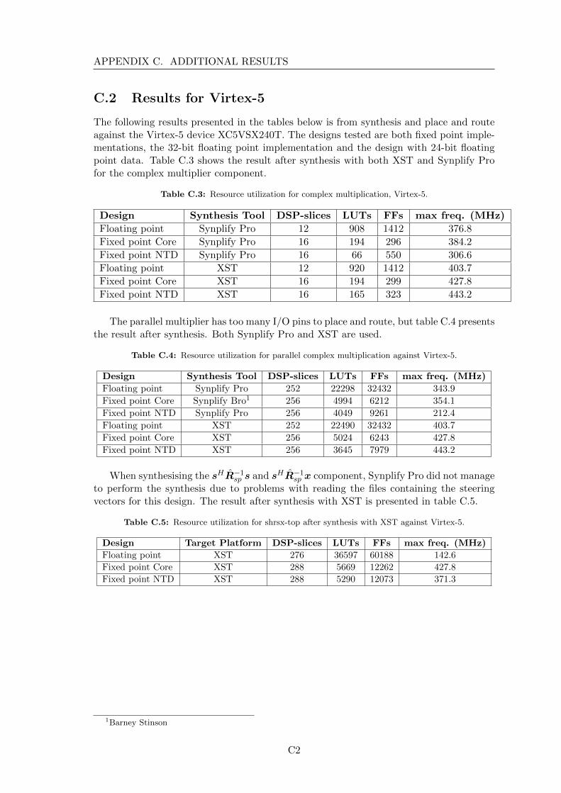
APPENDIX C. ADDITIONAL RESULTS
C.2 Results for Virtex-5
The following results presented in the tables below is from synthesis and place and routeagainst the Virtex-5 device XC5VSX240T. The designs tested are both fixed point imple-mentations, the 32-bit floating point implementation and the design with 24-bit floatingpoint data. Table C.3 shows the result after synthesis with both XST and Synplify Profor the complex multiplier component.
Table C.3: Resource utilization for complex multiplication, Virtex-5.
Design Synthesis Tool DSP-slices LUTs FFs max freq. (MHz)
Floating point Synplify Pro 12 908 1412 376.8
Fixed point Core Synplify Pro 16 194 296 384.2
Fixed point NTD Synplify Pro 16 66 550 306.6
Floating point XST 12 920 1412 403.7
Fixed point Core XST 16 194 299 427.8
Fixed point NTD XST 16 165 323 443.2
The parallel multiplier has too many I/O pins to place and route, but table C.4 presentsthe result after synthesis. Both Synplify Pro and XST are used.
Table C.4: Resource utilization for parallel complex multiplication against Virtex-5.
Design Synthesis Tool DSP-slices LUTs FFs max freq. (MHz)
Floating point Synplify Pro 252 22298 32432 343.9
Fixed point Core Synplify Bro1 256 4994 6212 354.1
Fixed point NTD Synplify Pro 256 4049 9261 212.4
Floating point XST 252 22490 32432 403.7
Fixed point Core XST 256 5024 6243 427.8
Fixed point NTD XST 256 3645 7979 443.2
When synthesising the sHR−1sp s and sHR−1
sp x component, Synplify Pro did not manageto perform the synthesis due to problems with reading the files containing the steeringvectors for this design. The result after synthesis with XST is presented in table C.5.
Table C.5: Resource utilization for shrsx-top after synthesis with XST against Virtex-5.
Design Target Platform DSP-slices LUTs FFs max freq. (MHz)
Floating point XST 276 36597 60188 142.6
Fixed point Core XST 288 5669 12262 427.8
Fixed point NTD XST 288 5290 12073 371.3
1Barney Stinson
C2