Embed Size (px)
Citation preview

1
Lecture 20: On-Wafer Sensors
Spanos & PoollaEE290H F03
1
In-chamber and on-wafer sensors
A Paradigm Shift
Lecture 20: On-Wafer Sensors
Spanos & PoollaEE290H F03
2
Overview
• Exact chamber environment control is relatively new• Various sensors (pressure, gas flow, gas composition,
temperature) are needed to accomplish it.• An interesting transition to “on-wafer” sensors holds
much promise...

2
Lecture 20: On-Wafer Sensors
Spanos & PoollaEE290H F03
3
Thermocouples• operating principle
Peltier-Seebeck effect, up to 3000o CT gradient along wires of different materials develop different emfemf measures junction Tplatinum rhodium alloy, or silicon based sensitivity 100-200µV /oK
• problemsbig problems with shield designradiative effectslow signal -- need amplifiers or use thermopileinvasivegas T measurement is very hard, especially < 10-4 torr
• commentsinexpensive, low drift low bandwidth
accuracy ~+/- 5oC at 800oC where do you want to measure T ?
Lecture 20: On-Wafer Sensors
Spanos & PoollaEE290H F03
4
Acoustic Wave sensors
• operating principle – acoustic wave is transmitted through body– surface and internal waves propagate through body at
T dependent speed– interference with source gives beats – beat frequency determines T
• issues– implementation difficulty – invasive– calibration
3
Lecture 20: On-Wafer Sensors
Spanos & PoollaEE290H F03
5
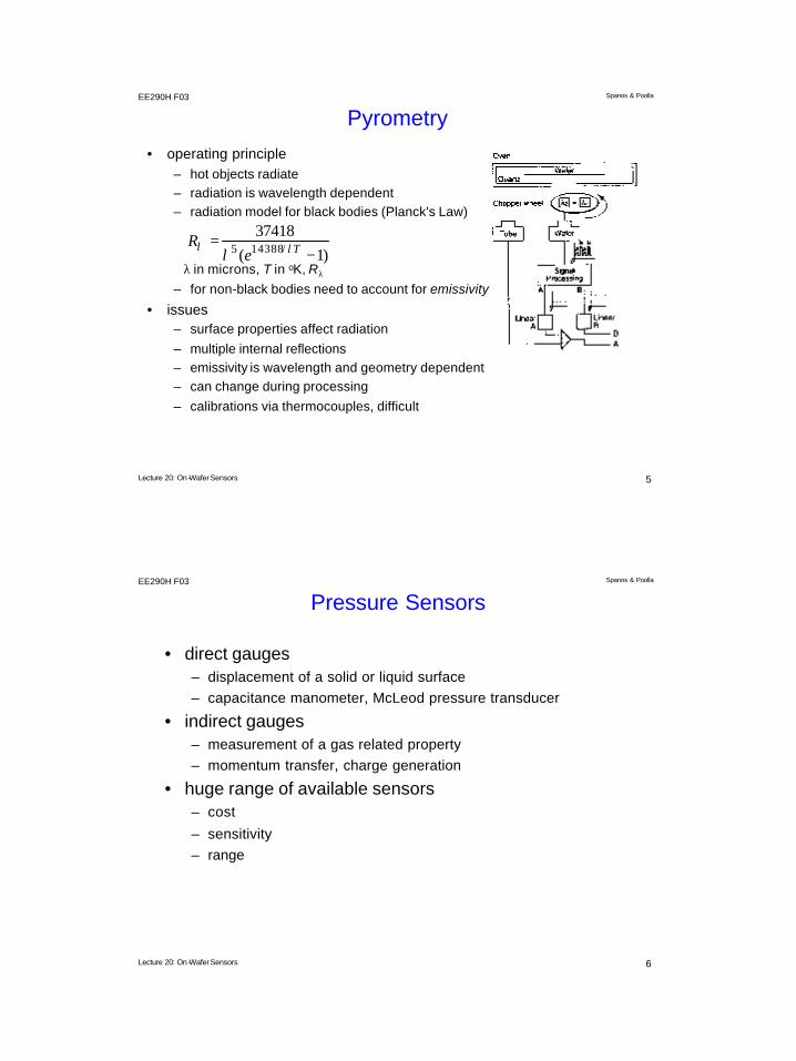
Pyrometry• operating principle
– hot objects radiate– radiation is wavelength dependent– radiation model for black bodies (Planck's Law)
λ in microns, T in oK, Rλ
– for non-black bodies need to account for emissivity
• issues– surface properties affect radiation– multiple internal reflections– emissivity is wavelength and geometry dependent– can change during processing– calibrations via thermocouples, difficult
)1(37418
/143885 −= Te
R λλλ
Lecture 20: On-Wafer Sensors
Spanos & PoollaEE290H F03
6
Pressure Sensors
• direct gauges– displacement of a solid or liquid surface– capacitance manometer, McLeod pressure transducer
• indirect gauges– measurement of a gas related property– momentum transfer, charge generation
• huge range of available sensors– cost
– sensitivity– range

4
Lecture 20: On-Wafer Sensors
Spanos & PoollaEE290H F03
7
Capacitance manometer
• basic idea– pressure differential causes
displacement of diaphragm– sense capacitance change
between diaphragm and fixed electrode
– resolution 10-2 %at 2 hertz and 10-3 torr
Lecture 20: On-Wafer Sensors
Spanos & PoollaEE290H F03
8
Gas flow meters• differential pressure meters• thermal mass flow meters
– mass flow = K / (T1 - T2)– K depends on specific heat of gas etc.– must be calibrated for different gases– accuracy ~ 1 sccm at flows of 40 sccm– low bandwidth because of thermal inertia
5
Lecture 20: On-Wafer Sensors
Spanos & PoollaEE290H F03
9
Mass Spectrometers
• two types– flux analyzers : sample gas through aperture– partial pressure sensors : analysis in exhaust stack
• issues– recombination in mass spec tube changes – indistinguishable species : (ex: CO, N2 and Si have
same amu (28))– pressure measurements are removed from
processing chamber
Lecture 20: On-Wafer Sensors
Spanos & PoollaEE290H F03
10
RGA• basic idea
special kind of mass spectrometermeasures gas compositions works at low vacuum < 10-5 torrion beam is produced from gas sample by e-bombardmentbeam is collimated by electric fields
q/m ratio of ions determines bending in B fielddetection of ions via a Faraday cup
• issuesquadrupole (magnetless design)very noisy !!good for diagnostics
can withstand 500 oCcan also be used at higher pressures with differential pumpsmass range 50 amu, resolution 2 amu,
6
Lecture 20: On-Wafer Sensors
Spanos & PoollaEE290H F03
11
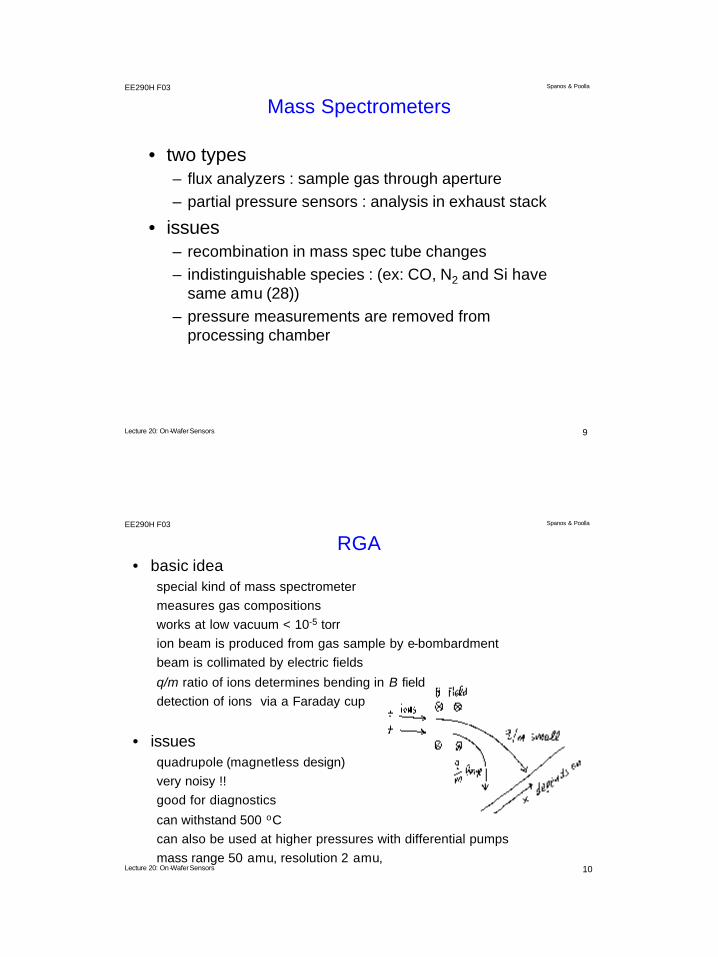
How about placing sensors on the wafer???
Sensarrayproducts
Lecture 20: On-Wafer Sensors
Spanos & PoollaEE290H F03
12
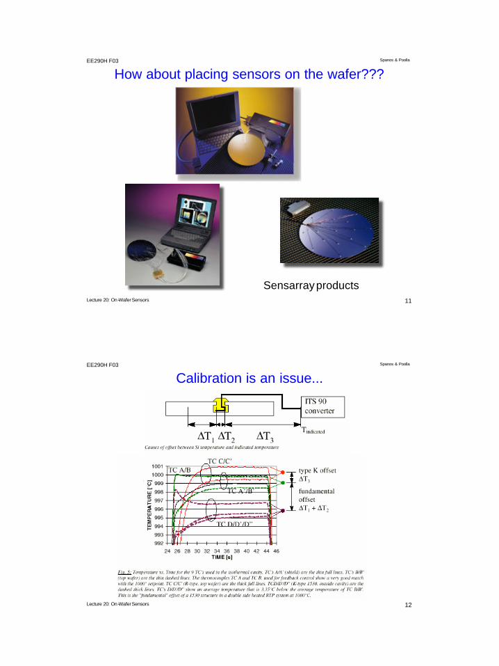
Calibration is an issue...

7
Lecture 20: On-Wafer Sensors
Spanos & PoollaEE290H F03
13
Long Term Reliability also an Issue...
Lecture 20: On-Wafer Sensors
Spanos & PoollaEE290H F03
14
On-Wafer Etch Rate by Resonant Structure
IEEE TRANSACTIONS ON SEMICONDUCTOR MANUFACTURING, VOL. 11, NO. 2, MAY 1998A Novel In Situ Monitoring Technique for Reactive Ion Etching Using a Surface Micromachined SensorMichael D. Baker, Frances R. Williams, Student Member, IEEE, and Gary S. May, Senior Member, IEEE

8
Lecture 20: On-Wafer Sensors
Spanos & PoollaEE290H F03
15
Remote reading of resonant sensor
Lecture 20: On-Wafer Sensors
Spanos & PoollaEE290H F03
16
Noise is the biggest problem...
On the bench... In the chamber...
When plasma is on...

9
Lecture 20: On-Wafer Sensors
Spanos & PoollaEE290H F03
17
But it works! (almost)
Innovative
noisy
intrusive
may contaminate...
Lecture 20: On-Wafer Sensors
Spanos & PoollaEE290H F03
18
Our VisionIn-situ sensor array, with integrated power and telemetry
Applications:process control, calibration, diagnostics & monitoring,process design
10
Lecture 20: On-Wafer Sensors
Spanos & PoollaEE290H F03
19
Issues
• Sensor arrays– inexpensive, modular– environmentally isolated– transparent to wafer handling robotics– on-board power & communications
• Operating mode– no equipment modifications !!– Smart “dummy” wafer for in-situ metrology
Lecture 20: On-Wafer Sensors
Spanos & PoollaEE290H F03
20
Test Case: Etch Rate
• Onboard etch-rate sensor for plasma etch– many sensor points on a wafer– accurate film thickness measurement– real-time data available– etch-friendly materials– wired power and communications (for now)

11
Lecture 20: On-Wafer Sensors
Spanos & PoollaEE290H F03
21
Transduction Scheme - Etch Rate
Van der Pauw structure: ρπ
=
VI
t2ln
Lecture 20: On-Wafer Sensors
Spanos & PoollaEE290H F03
22
Current Design
• Integrated Sensor Wafer Test Design• 57 etch-rate sensors on a 4” wafer• Full-wafer addressing of each sensor from a single die• Redundant interconnect to enhance yield• Four styles of sensor, selectable from a single die• On-board current-sourcing• Wired power and communications (at first)• Expandable to allow wireless power and communication
12
Lecture 20: On-Wafer Sensors
Spanos & PoollaEE290H F03
24
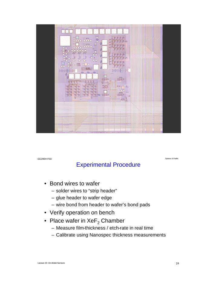
Experimental Procedure
• Bond wires to wafer– solder wires to “strip header”– glue header to wafer edge– wire bond from header to wafer’s bond pads
• Verify operation on bench• Place wafer in XeF2 Chamber
– Measure film-thickness / etch-rate in real time– Calibrate using Nanospec thickness measurements

13
Lecture 20: On-Wafer Sensors
Spanos & PoollaEE290H F03
25
Pictures
Lecture 20: On-Wafer Sensors
Spanos & PoollaEE290H F03
26
Pictures

14
Lecture 20: On-Wafer Sensors
Spanos & PoollaEE290H F03
27
Pictures
Lecture 20: On-Wafer Sensors
Spanos & PoollaEE290H F03
28
Pictures
15
Lecture 20: On-Wafer Sensors
Spanos & PoollaEE290H F03
29
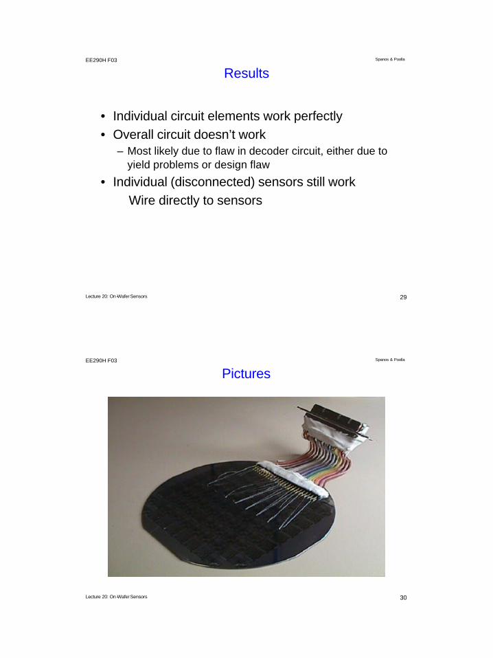
Results
• Individual circuit elements work perfectly• Overall circuit doesn’t work
– Most likely due to flaw in decoder circuit, either due to yield problems or design flaw
• Individual (disconnected) sensors still work⇒ Wire directly to sensors
Lecture 20: On-Wafer Sensors
Spanos & PoollaEE290H F03
30
Pictures

16
Lecture 20: On-Wafer Sensors
Spanos & PoollaEE290H F03
31
Pictures
Lecture 20: On-Wafer Sensors
Spanos & PoollaEE290H F03
32
Results
• 8 sensors (in a row) wired together in series• Everything works perfectly!• In-Situ XeF2 test performed
– XeF2 etch rate much too fast (~0.2µm/sec)– Sensor structure only 0.45 µm thick, gone in 2 sec– Sensors wired in series so when one etches through,
all measurements stop
⇒ Data collected during etch, but no calibration available

17
Lecture 20: On-Wafer Sensors
Spanos & PoollaEE290H F03
33
Data - Etch #1
0 5 10 15 2 0 2 5 3 00
1000
2000
3000
4000
5000P o l y s i l i c o n T h i c k n e s s v s . T i m e f o r E x p e r i m e n t # 1
T i m e ( s e c )
Me
asu
red
Th
ickn
ess
(A
)
0 5 10 15 2 0 2 5 3 00
100
200
300
400
500Po l ys i l i con E t ch -Ra te vs . T ime f o r Expe r imen t #1
T i m e ( s e c )
Filt
ere
d E
tch
-Ra
te (
A/s
ec)
Lecture 20: On-Wafer Sensors
Spanos & PoollaEE290H F03
34
Data - Etch #2
0 2 4 6 8 1 0 1 20
1000
2000
3000
4000
5000Po l ys i l i con Th i ckness vs . T ime fo r Expe r imen t #2
T ime (sec )
Me
asu
red
Th
ickn
ess
(A
)
0 2 4 6 8 1 0 1 20
500
1000
1500
2000
2500
3000
3500Po lys i l i con E tch -Ra te vs . T ime fo r Exper imen t #2
T ime (sec )
Filt
ere
d E
tch
-Ra
te (
A/s
ec)

18
Lecture 20: On-Wafer Sensors
Spanos & PoollaEE290H F03
35
Data - Etch #3
0 1 2 3 4 5 6 7 8 9 100
1 0 0 0
2 0 0 0
3 0 0 0
4 0 0 0
5 0 0 0Po lys i l i con Th i ckness vs . T ime fo r Expe r imen t #3
T ime (sec)
Me
asu
red
Th
ickn
ess
(A
)
0 1 2 3 4 5 6 7 8 9 100
5 0 0
1 0 0 0
1 5 0 0
2 0 0 0Po l ys i l i con E t ch -Ra te vs . T ime f o r Expe r imen t #3
T ime (sec)
Filt
ere
d E
tch
-Ra
te (
A/s
ec)
Lecture 20: On-Wafer Sensors
Spanos & PoollaEE290H F03
36
Plan
• Design new sensor wafer with no onboard electronics, only sensors
• Simple process ⇒ one week turnaround time instead of one year
• Add several features– Polysilicon “guard ring” around sensors to reduce
XeF2 etch rate by “loading” the etcher– Larger sensors to allow in-situ reflectometry– Clip-on wires to decrease time-to-experiment– Parallel connection of sensors, for better reliability

19
Lecture 20: On-Wafer Sensors
Spanos & PoollaEE290H F03
38
How about completely wireless???
20
Lecture 20: On-Wafer Sensors
Spanos & PoollaEE290H F03
39
Lecture 20: On-Wafer Sensors
Spanos & PoollaEE290H F03
40
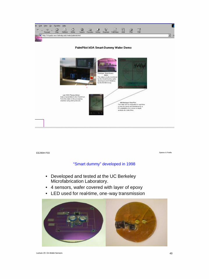
“Smart dummy” developed in 1998
• Developed and tested at the UC Berkeley Microfabrication Laboratory.
• 4 sensors, wafer covered with layer of epoxy• LED used for real-time, one-way transmission
21
Lecture 20: On-Wafer Sensors
Spanos & PoollaEE290H F03
41
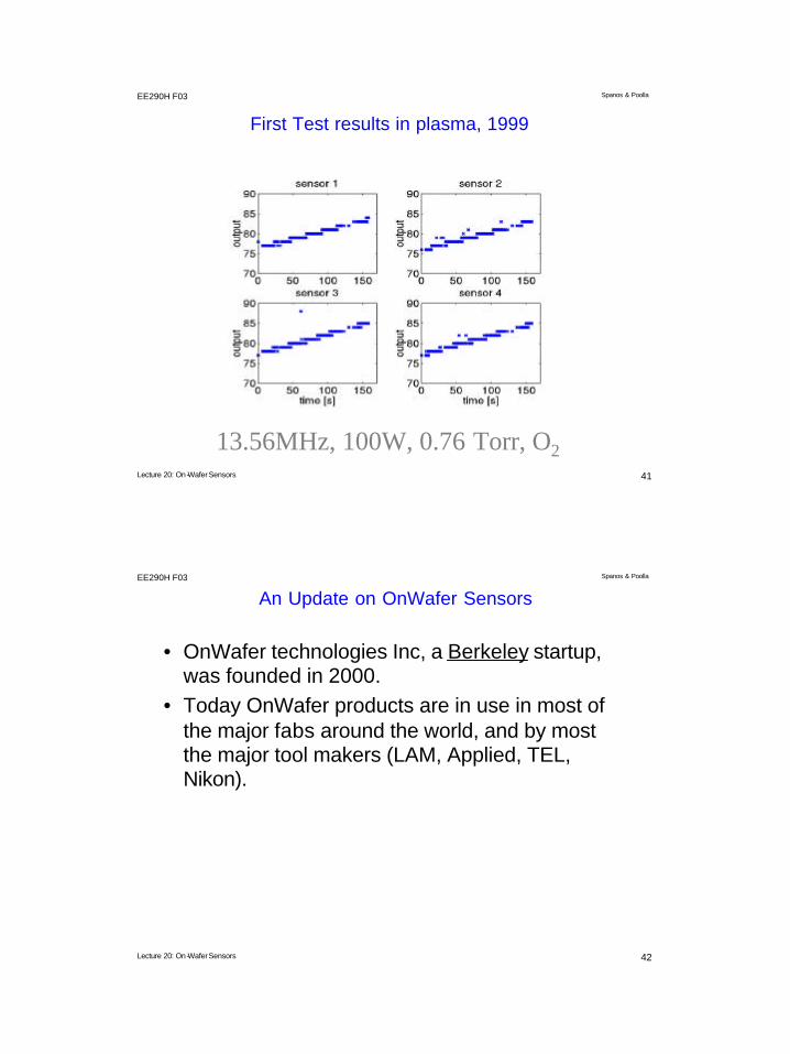
First Test results in plasma, 1999
13.56MHz, 100W, 0.76 Torr, O2
Lecture 20: On-Wafer Sensors
Spanos & PoollaEE290H F03
42
An Update on OnWafer Sensors
• OnWafer technologies Inc, a Berkeley startup, was founded in 2000.
• Today OnWafer products are in use in most of the major fabs around the world, and by most the major tool makers (LAM, Applied, TEL, Nikon).

22
Lecture 20: On-Wafer Sensors
Spanos & PoollaEE290H F03
43
Present OnWafer System
IR DongleIR Dongle
Base StationBase Station
SensorWaferSensorWafer
ShipperShipper
Lecture 20: On-Wafer Sensors
Spanos & PoollaEE290H F03
44
feedbackprocess control
processingequipment
data
OnWafer
base station
The Approach
wafers to be processed
23
Lecture 20: On-Wafer Sensors
Spanos & PoollaEE290H F03
45
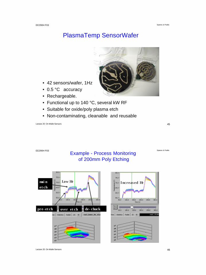
• 42 sensors/wafer, 1Hz• 0.5 °C accuracy• Rechargeable. • Functional up to 140 °C, several kW RF• Suitable for oxide/poly plasma etch• Non-contaminating, cleanable and reusable
PlasmaTemp SensorWafer
Lecture 20: On-Wafer Sensors
Spanos & PoollaEE290H F03
46
Example - Process Monitoringof 200mm Poly Etching
Increased HeLow He
pre-etch
main
etch
de-chuckover etch

24
Lecture 20: On-Wafer Sensors
Spanos & PoollaEE290H F03
47
Example - Gas flow trouble in TEL DRM Etcher
“before” data is hotter, further, the pre-etch step is significantly less uniform…“before” data is hotter, further, the pre-etch step is significantly less uniform…
Lecture 20: On-Wafer Sensors
Spanos & PoollaEE290H F03
48
Example - Comparison between 8 PEB plates on a 193nm wafer track
11 12 13 14 21 22 23 24
Best!
Worst!
Data collection in two 10-minute cassette-to-cassette missionsData collection in two 10-minute cassette-to-cassette missions

25
Lecture 20: On-Wafer Sensors
Spanos & PoollaEE290H F03
49
On-Wafer PEB / CD Analysis
P6P6P5P5P4P4P3P3P2P2P1P1
Six TEL ACT 8 plates used for 90nm CD lines (193nm Lithography)Six TEL ACT 8 plates used for 90nm CD lines (193nm Lithography)
Lecture 20: On-Wafer Sensors
Spanos & PoollaEE290H F03
50
Analyzing PEB Plates using BakeInfo
Overshoot
Cooling
Steady
Heating
Chill
200mm ArF90nm
130oC 60sec