Embed Size (px)
Citation preview

Dat
a sh
eet
¸In-Circuit Test Option for ¸CompactTSVPusing ¸TS-PSAM, ¸TS-PICT, ¸TS-PMB and Software ¸TS-LEGT, ¸TS-LEG2
Complete analog in-circuit measure-ment unit with ¸TS-PSAM and ¸TS-PICT
Test of R, L, C, diodes, transistors, parallel R-C
Guarded resistor measurements (3-, 4-, 6-wire)
Guarded impedance measurements (3-, 4-, 6-wire)
Measurement frequencies 100 Hz, 1 kHz, 10 kHz for impedance tests
Low stimulus voltage for isolation of diodes and ICs
Test system based on CompactPCI, PXI and CAN
Up to 300 tested parts per second Automatic test generator with circuit
analysis and testability check
Standard interface for CAD data import
Easy-to-use EGTSL environment for in-circuit test debugging
Up to 900 test pins in single-chassis ¸CompactTSVP
Up to 2250 test pins in dual-chassis ¸CompactTSVP/¸PowerTSVP solution
Version
01.00
September
2004
ICT Option_en.indd 1 23.09.2004 11:13:38

2 ¸In-Circuit Test Option for ¸CompactTSVP
Product introduction
Continuing the ¸CompactTSVP prod-uct family’s philosophy of scalability and fl exibility, a modular and cost-effective in-circuit test (ICT) platform can also be easily created using hardware and soft-ware from the ¸CompactTSVP prod-uct portfolio.
The ¸ICT Option provides a wide variety of standardized test methods and combinations. To meet each customer‘s requirements, the classic analog ICT can be merged with all functional tests (FCT) offered by the ¸CompactTSVP fami-ly as well as with the entire spectrum of products from the PXI and cPCI market.
The ¸ICT Option is based on the CompactPCI measurement and stim-ulus modules ¸TS-PSAM and ¸TS-PICT. Each module takes up only one slot in the ¸Com-pactTSVP and has a fl oating power sup-ply as a rear I/O module. The ¸TS-
PICT expands the Analog Source and Measurement Module ¸TS-PSAM to provide fully analog ICT capability. In ICTs and FCTs, the DUT’s test pins are routed via the Switching Matrix Module ¸TS-PMB and the Rohde & Schwarz measurement bus to the ¸TS-PICT and ¸TS-PSAM measurement units. Therefore, the same test pins can be used for ICTs and FCTs. A standard-ized fi xture interface (¸TS-PAD3/¸TS-F3F), directly mounted on the ¸CompactTSVP chassis, provides high signal quality to the fi xture.
Typical applications
Since the ICT functionality is divided into different modules, the modular ICT op-tion can be precisely confi gured to the customer‘s requirements. Applications may vary from an FCT enhancement to a classic analog ICT solution.
The ICT expansion provides the following benefi ts, especially for the FCT:
A contact test checks whether the contacts with the DUT (wiring test) are functioning properly
A shorts test prevents the DUT or the test system from being destroyed during power-up
A continuity test detects open signal paths
When the modular ICT option is used, even a full ICT system can be confi gured, thus providing the following features:
Automated test generation Highest fl exibility in terms of
scalability and functionality Excellent test speed State-of-the-art graphics-based
debugging environment
In addition, the implementation of the industry standards PXI and CompactPCI ensures that FCT methods can be added regardless of vendor.
ICT Option_en.indd 2 23.09.2004 11:13:56

¸In-Circuit Test Option for ¸CompactTSVP 3
Wiring the adapter is simplifi ed by the full matrix of the Switching Matrix Module ¸TS-PMB in the case of 2-wire and 4-wire techniques. This module is con-trolled by the controller area net-work (CAN) bus, which has already proven itself to be a rugged bus system in the automotive market. The pin count is scalable in steps of 90 pins.
Hardware
For ICTs, the following measure-ment tasks are performed by the ¸TS-PSAM:
Discharge of capacitors and printed boards
Contact test Shorts test Continuity test 2-wire and 4-wire resistance
measurements (DC) Measurement hardware for
system selftest
In addition, the ¸TS-PSAM covers essential FCT requirements:
Current/voltage measurement Data acquisition (i.e. waveform
recording) Trigger/clock generation
In conjunction with the ¸TS-PICT, guarded measure-ments can also be performed:
Resistor, capacitor, inductor (AC) tests
3-, 4- and 6-wire resistance (DC) and impedance measurements (AC)
Diode and transistor tests
Couplingrelays
ABA1
ABC2
ABB1
ABB2
ABA2
ABC1
ABD2
ABD1
Analog bus (AB)
LABA
1
LABC
2
LABB
1
LABB
2
LABA
2
LABC
1
LABD
2
LABD
1
¸TS-PSAM
RACH1 to RACH4
CHA-GND
IL1, IL2
GND
DCS
Voltage and current source
DCS_HI
MU_HI
MU_LO
DCH
Discharge unit
DCH_HI
Local analog bus (LABA1 to LABD2, GND)
MU_SHIMU_SLO
RACOMRBCOM
PXI_TRIG0 to PXI_TRIG7
XTI1, XTI2XTO1, XTO2
AUX1, AUX2Trigger
AUX1, AUX2
XTA1, XTA2Isolation
MU
Voltage and current mea- surement unit
DCS_SHIDCS_SLODCS_LO
RBCH1 to RBCH4
Block diagram of the Analog Source and Measurement Module ¸TS-PSAM
Primarymatrix
Couplingrelays
AOSAC stimulus
DC offset source
CMUCurrent
measurementunit
REF
AOS_HI
CMU_HICMU_SHICMU_SLO
GND
REF_RREF_LREF_CREF_COM
ABA1
ABC2
ABB1
ABB2
ABA2
ABC1
ABD2
ABD1
Analog bus (AB)
LABA
1
LABC
2
LABB
1
LABB
2
LABA
2
LABC
1
LABD
2
LABD
1¸TS-PICT
GND
Block diagram of the In-Circuit Test (ICT) Extension Module ¸TS-PICT
Couplingrelays
ABA1
ABC2
ABB1
ABB2
ABA2
ABC1
ABD2
ABD1
Analog bus (AB)
LABA
1
LABC
2
LABB
1
LABB
2
LABA
2
LABC
1
LABD
2
LABD
1
¸TS-PMB
L1L2
IL1IL2IL3
Instru-mentation
lines
GND
Local analog bus (LAD)P1P2P3P4
P89P90
PIN relays
Sense relays
RAM
CAN
SPI
Rela
y co
ntol
Microcontroller
PXI trigger logic
GNDGND
CHA-GND
GNDNOGNDlines
Block diagram of the Switching Matrix Module ¸TS-PMB
ICT Option_en.indd 3 23.09.2004 11:14:14

4 ¸In-Circuit Test Option for ¸CompactTSVP
In highly complex test cases, the com-bined use of all modules yields a high-ly sophisticated virtual instrument. The ¸CompactTSVP backplane links the different modules together with CAN, cPCI and PXI buses. The analog mea-surement backplane is separated from the digital backplane to provide high-quality and reproducible analog signal routing.
Parallel components in a DUT circuit and test system residuals are compensat-ed for by using guarding, sensing and phase-correct measurement technology.
Software
ICT programs are generated automati-cally by the Automatic Test Generator (ATG), which creates a test proposal in XML format directly from the CAD data interface (BDL fi le format).
The well-structured graphical user inter-face, which is highly intuitive for any-one with experience in Windows-based applications, makes debugging and opti-mization quick and easy.
The high-speed tests, typically only 3 ms per part, are performed using a special precompiling algorithm of the Enhanced Generic Test Software Library (EGTSL).
Schematic diagram of a guarded impedance test
This algorithm analyzes the test sequence and generates very effi cient meta-code when saving the program (e.g. optimiza-tion of range switches, selection of bus lines).
The simple execution of the ICT runtime via DLL calls from any sequencer software ensures fl exible and straightforward in-tegration into the software environment.
Flow chart of the ICT program generation
Automated
test generationDebugging
Execution/
Runtime
The ICT program is implemented in the FCT like a normal test step.
The ¸TS-LEG2 software, which is a subset of ¸TS-LEGT, supports the ba-sic ICT functions. These functions can be performed only by the ¸TS-PSAM (discharge, contact, shorts, continuity, 2-wire and 4-wire resistance).
Automated test generation
ICT programs are generated automat-ically by the Automatic Test Generator (ATG). The ATG analyzes the DUT cir-cuit described in CAD data (BDL fi le for-mat). Appropriate test and guard points are selected automatically. Test require-ments and available tester confi gura-tions are compared, and resulting test-ability problems are reported. An exe-cutable ICT program that can be run by EGTSL is generated. The wiring of the DUT can be started immediately using the wiring fi le that has been created.
Program generation by the Automatic Test Generator (ATG)
Automatic
Test Generator
ATG
CADinterface
Testerconfiguration
Wiringlist
ICTprogram
Report oftestability
OUTP
UT
INPU
T
¸TS-PSAMV
Matrix ¸TS-PMB
DUT
Zx
Z1
Z2
¸TS-PICT
A
~
ICT Option_en.indd 4 23.09.2004 11:14:18

¸In-Circuit Test Option for ¸CompactTSVP 5
Debugging environment
The EGTSL debugging environment has the familiar look of modern Windows applications. With this graphical user interface, virtually anyone can quick-ly master the full spectrum of function-ality and settings provided by EGTSL. There is no need to learn a special pro-gramming language or work with a pre-defi ned screen layout. Test engineers can create their own desktop and dis-play all required information on one screen. They can scale, move, and dis-play the windows as needed.
Even implementing a new test step is like creating a new folder in Windows Explorer, whose tree structure is similar to the ICT program fl ow in EGTSL.
Within the EGTSL debugging environ-ment, users can do the following:
Create, delete or move test steps by a mouse click or drag and drop
Change settings of test steps, e.g. limits, test method, stimuli and mea-surement
Defi ne specifi c timing models
Use compiler functionalities such as setting breakpoints, step into or over certain test steps
Defi ne and handle different variants Export and import limits Use statistical tools such as histo-
grams to verify stable results Display a detailed test report Create the core program for the panel
test
EGTSL debugging environment
ICT Option_en.indd 5 23.09.2004 11:14:22

6 ¸In-Circuit Test Option for ¸CompactTSVP
Execution/Runtime
A separate sequencing program for the ICT option from Rohde & Schwarz is not needed. The ICT runtime can directly handle the customer‘s sequencer soft-ware, already used in the FCT.
The EGTSL is executed by a DLL call from the test sequencer (e.g. off-the-shelf test sequencer or dedicated executable soft-ware).
The test hardware is automatically man-aged by the resource manager, which handles the information available in the tester confi guration fi les (PHYSICAL.INI and APPLICATION.INI).
Special failure routines or variant set-tings are covered by the entire function-ality of the sequencing program. There-fore, each time a DLL call is performed, variants defi ned in the ICT program can be selected and each subtree can be executed independently.
ICT program integrated into a functional test
Test Sequence
FCT..................
FCT..................
variantssubtrees
A complete test result containing the information of the ICT and FCT can be generated by the sequencer due to handover of the ICT failure count. Additionally, a detailed ICT report can be generated.
ICT Option_en.indd 6 23.09.2004 11:14:30

¸In-Circuit Test Option for ¸CompactTSVP 7
Confi gurations
A single-chassis ¸CompactTSVP (¸TS-PCA3) can be confi gured with up to 900 test pins (ten ¸TS-PMB modules). A dual-chassis confi guration can provide an additional 1350 test pins with up to 15 Switching Matrix Modules ¸TS-PMB in the ¸PowerTSVP (¸TS-PWA3), yielding a maximum of 2250 test pins.
Several test system confi gurations are possible:
“One box“ ICT with up to 900 test pins and classic analog ICT functionality
“One box“ FCT/ICT solution with a mix-ture of FCT and ICT modules
Dual-chassis FCT/ICT test system with measurement modules in the
¸TS-PCA3 and switching modules up to 1350 pins in the ¸TS-PWA3; DUT fi xturing via the ¸TS-PWA3
Dual-chassis ICT with up to 2250 pins and full analog ICT functionality
Test fi xture accessories
To accelerate integration of the ¸CompactTSVP into production test environments in a quick and cost- effective manner, an entire set of mass-interconnection support products has been created. The platform modules are equipped with a 96-pin DIN 41612 con-nector which is easy to handle in fi xture wiring using wire-wrap techniques.
The interface between the Receiver Frame ¸TS-PAD3 and the Fixture Frame ¸TS-F3F is provid-ed by the modular Connector Carriers ¸TS-PAX1 on the test instru-ment side and the Connector Carriers ¸TS-F3X1 on the fi xture side. Option-al, spring-loaded precision contacts can be mounted.
¸TS-PAD3
¸TS-PAX1 ¸TS-F3X1
¸TS-F3F DUT with bed of nails
Test fi xture accessories
A vacuum control unit (¸TS-PVAC) with single or dual vacuum ports is direct-ly controlled by the ¸CompactTSVP.
Security through selftest and diagnostic features
The built-in selftest capabilities range from fast diagnostics to complete, auto-mated evaluations of all relays and switch
paths. The use of the ¸TS-PSAM allows a fast and comprehensive “in-system“ selftest to be performed.
Diagnostic LEDs on the module front panel speed up installation and immedi-ately indicate proper operation.
For all dual-chassis confi gura-tions, the ¸CompactTSVP and PowerTSVP have to be connected via the analog measurement bus exten-sion cable (¸TS-PK01) and the CAN bus control cable (¸TS-PK02).
Analogbus
CANbus
Combination of the ¸TS-PWA3 and ¸TS-PCA3 to form a fully analog ICT with 2250 pins
ICT Option_en.indd 7 23.09.2004 11:14:44

8 ¸In-Circuit Test Option for ¸CompactTSVP
Application in ¸CompactTSVP / PowerTSVP
¸CompactTSVP one slot for ¸TS-PSAMone slot for ¸TS-PICTup to ten slots for ¸TS-PMB
¸PowerTSVP (optional) up to 15 slots for ¸TS-PMB
Interface
Control bus CompactPCI/PXI busCAN 2.0B for ¸TS-PMB
DUT connector (front) DIN 41612, 96 pins on ¸TS-PSAM, ¸TS-PMB
Tolerances of specifi ed values apply under the following conditions:
Recommended calibration period 1 year
Temperature range 23 °C ±5 °C
Additional error specifi ed by the temperature coeffi cient in the range 5 °C to 18 °C and 28 °C to 40 °C
Resistor tests (DC)Resistor test, non-guarded (¸TS-PSAM)
Range Error limit Source voltage
(minimum)
Source current
(minimum)
Mode 1) Wires Average Sample interval
0.1 Ω to 1 Ω 1.0 + 5.0 mΩ 2) 0.5 V 100 mA C 4 20 1 ms
1 Ω to 10 Ω 1.5 3) 0.2 V 10 mA C 4 20 1 ms
10 Ω to 100 Ω 0.5 3) 0.2 V 25 mA V 4
100 Ω to 1 kΩ 0.5 3) 0.2 V 2.5 mA V 4
1 kΩ to 10 kΩ 0.5 3) 0.2 V 1.0 mA V 2
10 kΩ to 100 kΩ 1.0 3) 0.2 V 0.1 mA V 2 100 5 µs
100 kΩ to 1 MΩ 1.0 3) 1.0 V 0.1 mA V 2 20 1 ms
1 MΩ to 10 MΩ 1.0 3) 5.0 V 0.1 mA V 2 20 1 ms
1) C = current injection, voltage measurement.V = voltage injection, current measurement.
2) Error limit: ± (% of reading + absolute value).Temperature coeffi cient: ±(0.1 × accuracy) / °C.
3) Error limit: ± % of reading.Temperature coeffi cient: ±(0.1 × accuracy) / °C.
Resistor test, guarded (¸TS-PSAM, ¸TS-PICT)
Guard ratio (R1: R
x, R
2 : R
x) Error limit 1) Range (R
1 and R
2) Source Mode 2) Wires
1 : 1 0.5 10 Ω to 100 Ω 0.2 V V 6
1 : 10 1.0 10 Ω to 100 Ω 0.2 V V 6
1 : 100 1.0 10 Ω to 100 Ω 1.0 V V 6
1 : 1000 7.0 10 Ω to 100 Ω 1.0 V V 6
1 : 1 0.5 100 Ω to 1 kΩ 0.2 V V 6
1 : 10 0.5 100 Ω to 1 kΩ 0.2 V V 6
1 : 100 1.0 100 Ω to 1 kΩ 1.0 V V 6
1 : 1000 7.0 100 Ω to 1 kΩ 1.0 V V 6
1) Error limit: ± % of reading.Temperature coeffi cient: ±(0.1 × accuracy) / °C.
3) V = voltage injection, current measurement.
Specifi cations
Resistor test, guarded
Rx
Stimulusnode
Measurementnode
Guard node
R1 R2R2
Guard ratio:R1 / Rx = R2 / Rx
ICT Option_en.indd 8 23.09.2004 11:15:41
¸In-Circuit Test Option for ¸CompactTSVP 9
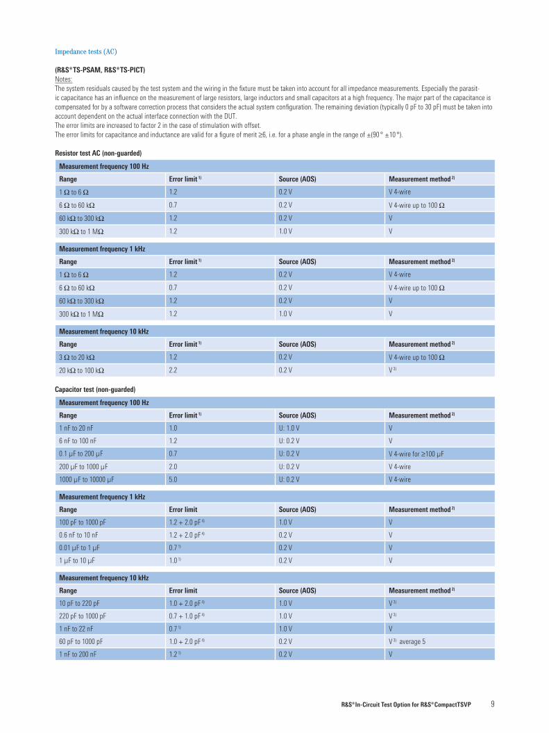
Impedance tests (AC)
(¸TS-PSAM, ¸TS-PICT)
Notes:The system residuals caused by the test system and the wiring in the fi xture must be taken into account for all impedance measurements. Especially the parasit-ic capacitance has an infl uence on the measurement of large resistors, large inductors and small capacitors at a high frequency. The major part of the capacitance is compensated for by a software correction process that considers the actual system confi guration. The remaining deviation (typically 0 pF to 30 pF) must be taken into account dependent on the actual interface connection with the DUT.The error limits are increased to factor 2 in the case of stimulation with offset.The error limits for capacitance and inductance are valid for a fi gure of merit ≥6, i.e. for a phase angle in the range of ±(90 ° ±10 °).
Resistor test AC (non-guarded)
Measurement frequency 100 Hz
Range Error limit 1) Source (AOS) Measurement method 2)
1 Ω to 6 Ω 1.2 0.2 V V 4-wire
6 Ω to 60 kΩ 0.7 0.2 V V 4-wire up to 100 Ω
60 kΩ to 300 kΩ 1.2 0.2 V V
300 kΩ to 1 MΩ 1.2 1.0 V V
Measurement frequency 1 kHz
Range Error limit 1) Source (AOS) Measurement method 2)
1 Ω to 6 Ω 1.2 0.2 V V 4-wire
6 Ω to 60 kΩ 0.7 0.2 V V 4-wire up to 100 Ω
60 kΩ to 300 kΩ 1.2 0.2 V V
300 kΩ to 1 MΩ 1.2 1.0 V V
Measurement frequency 10 kHz
Range Error limit 1) Source (AOS) Measurement method 2)
3 Ω to 20 kΩ 1.2 0.2 V V 4-wire up to 100 Ω
20 kΩ to 100 kΩ 2.2 0.2 V V 3)
Capacitor test (non-guarded)
Measurement frequency 100 Hz
Range Error limit 1) Source (AOS) Measurement method 2)
1 nF to 20 nF 1.0 U: 1.0 V V
6 nF to 100 nF 1.2 U: 0.2 V V
0.1 µF to 200 µF 0.7 U: 0.2 V V 4-wire for ≥100 µF
200 µF to 1000 µF 2.0 U: 0.2 V V 4-wire
1000 µF to 10000 µF 5.0 U: 0.2 V V 4-wire
Measurement frequency 1 kHz
Range Error limit Source (AOS) Measurement method 2)
100 pF to 1000 pF 1.2 + 2.0 pF 4) 1.0 V V
0.6 nF to 10 nF 1.2 + 2.0 pF 4) 0.2 V V
0.01 µF to 1 µF 0.7 1) 0.2 V V
1 µF to 10 µF 1.0 1) 0.2 V V
Measurement frequency 10 kHz
Range Error limit Source (AOS) Measurement method 2)
10 pF to 220 pF 1.0 + 2.0 pF 4) 1.0 V V 3)
220 pF to 1000 pF 0.7 + 1.0 pF 4) 1.0 V V 3)
1 nF to 22 nF 0.7 1) 1.0 V V
60 pF to 1000 pF 1.0 + 2.0 pF 4) 0.2 V V 3) average 5
1 nF to 200 nF 1.2 1) 0.2 V V
ICT Option_en.indd 9 23.09.2004 11:15:42

10 ¸In-Circuit Test Option for ¸CompactTSVP
Inductance test (non-guarded)
Measurement frequency 100 Hz
Range Error limit 1) Source (AOS) Measurement method 2) 5)
1 mH to 20 mH 3.0 0.2 V V
20 mH to 30 H 2.0 0.2 V V
30 H to 100 H 5.0 0.2 V V
Measurement frequency 1 kHz
Range Error limit 1) Source (AOS) Measurement method 2) 5)
250 µH to 2 mH 3.0 0.2 V V
2 mH to 3 H 2.0 0.2 V V
3 H to 10 H 2.0 0.2 V V
Measurement frequency 10 kHz
Range Error limit Source (AOS) Measurement method 2) 5)
60 µH to 1 H 2.0 1) 1.0 V V
25 µH to 70 µH 2.0 + 1.0 µH 4) 0.2 V V 4-wire
70 µH to 50 mH 3.0 1) 0.2 V V
1) Error limit: ± % of reading.Temperature coeffi cient: ±(0.1 × accuracy) / °C.
2) V = voltage injection, current measurement.3) Min. current limit 20 µA.4) Error limit: ±(% of reading + absolute value).
Temperature coeffi cient: ±(0.1 × accuracy) / °C.5) For 1 mH to 2 H: measurement delay = 0.4 × L [s/H].
For 2 H to 100 H: measurement delay = 1 s.
Contact test
¸TS-PSAM
Source voltage 1 V to 5 V
Level 1 kΩ to 1 MΩ
Shorts / continuity test
¸TS-PSAM
Source voltage 0.1 V to 0.5 V
Level 1 Ω to 1 kΩ
Discharge circuit
¸TS-PSAM
Max. input voltage 125 V
Max. discharge current (typ.)
V > 13 V 10 mA
V < 13 V 150 mA
V < 7 V 300 mA
V < 4.5 V 450 mA
Diode / transistor test
¸TS-PSAM, ¸TS-PICT
Leakage current 0.1 µA to 100 mA
Forward voltage 0 V to 5 V
Relay multiplexer
¸TS-PMB
Number of pins per module 90
Number of pins per system 900 in ¸TS-PCA3, 2250 in combination ¸TS-PCA3 /¸TS-PWA3
Analog bus access
¸TS-PSAM, ¸TS-PICT, ¸TS-PMB
Analog bus access 8 buses
Max. voltage DC/AC 125 V / 90 V rms
Max. current DC/AC 1 A / 1 A rms
Max. switching power 10 W / 10 VA
ICT Option_en.indd 10 23.09.2004 11:15:42
¸In-Circuit Test Option for ¸CompactTSVP 11
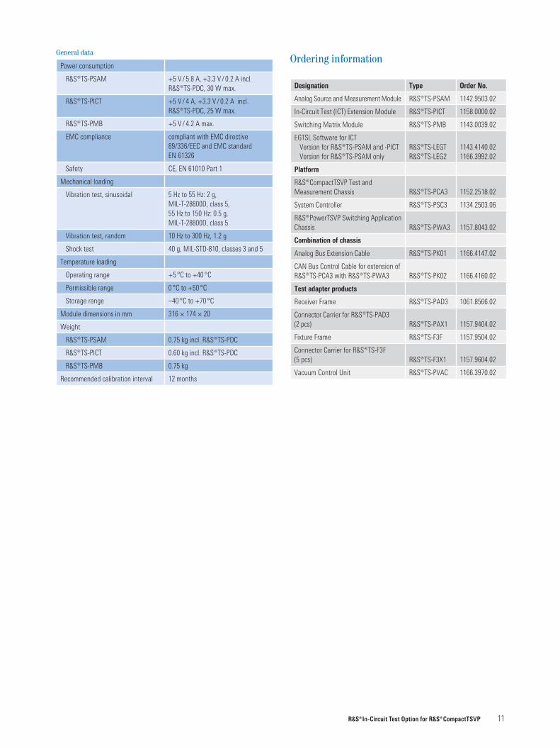
General data
Power consumption
¸TS-PSAM +5 V / 5.8 A, +3.3 V / 0.2 A incl. ¸TS-PDC, 30 W max.
¸TS-PICT +5 V / 4 A, +3.3 V / 0.2 A incl. ¸TS-PDC, 25 W max.
¸TS-PMB +5 V / 4.2 A max.
EMC compliance compliant with EMC directive 89/336/EEC and EMC standard EN 61326
Safety CE, EN 61010 Part 1
Mechanical loading
Vibration test, sinusoidal 5 Hz to 55 Hz: 2 g, MIL-T-28800D, class 5, 55 Hz to 150 Hz: 0.5 g, MIL-T-28800D, class 5
Vibration test, random 10 Hz to 300 Hz, 1.2 g
Shock test 40 g, MIL-STD-810, classes 3 and 5
Temperature loading
Operating range +5 °C to +40 °C
Permissible range 0 °C to +50 °C
Storage range –40 °C to +70 °C
Module dimensions in mm 316 × 174 × 20
Weight
¸TS-PSAM 0.75 kg incl. ¸TS-PDC
¸TS-PICT 0.60 kg incl. ¸TS-PDC
¸TS-PMB 0.75 kg
Recommended calibration interval 12 months
Ordering information
Designation Type Order No.
Analog Source and Measurement Module ¸TS-PSAM 1142.9503.02
In-Circuit Test (ICT) Extension Module ¸TS-PICT 1158.0000.02
Switching Matrix Module ¸TS-PMB 1143.0039.02
EGTSL Software for ICTVersion for ¸TS-PSAM and -PICTVersion for ¸TS-PSAM only
¸TS-LEGT¸TS-LEG2
1143.4140.021166.3992.02
Platform
¸CompactTSVP Test and Measurement Chassis ¸TS-PCA3 1152.2518.02
System Controller ¸TS-PSC3 1134.2503.06
¸PowerTSVP Switching Application Chassis ¸TS-PWA3 1157.8043.02
Combination of chassis
Analog Bus Extension Cable ¸TS-PK01 1166.4147.02
CAN Bus Control Cable for extension of ¸TS-PCA3 with ¸TS-PWA3 ¸TS-PK02 1166.4160.02
Test adapter products
Receiver Frame ¸TS-PAD3 1061.8566.02
Connector Carrier for ¸TS-PAD3 (2 pcs) ¸TS-PAX1 1157.9404.02
Fixture Frame ¸TS-F3F 1157.9504.02
Connector Carrier for ¸TS-F3F (5 pcs) ¸TS-F3X1 1157.9604.02
Vacuum Control Unit ¸TS-PVAC 1166.3970.02
ICT Option_en.indd 11 23.09.2004 11:15:42

¸is
a re
gist
ered
trad
emar
k of
Roh
de &
Sch
war
z Gm
bH &
Co.
KG
· Tra
de n
ames
are
trad
emar
ks o
f the
ow
ners
· Pr
inte
d in
Ger
man
y (P
e bb
)PD
075
8.19
64.3
2 · ¸
In-C
ircui
t Tes
t Opt
ion
for ¸
Com
pact
TSVP
· Ve
rsio
n 01
.00
· Sep
tem
ber 2
004
· Dat
a w
ithou
t tol
eran
ce li
mits
is n
ot b
indi
ng ·
Subj
ect t
o ch
ange
www.rohde-schwarz.com Europe: Tel: +49 1805 12 4242, e-mail: [email protected] · USA: Tel. +1 410-910-7988, e-mail: [email protected]
Asia: Tel. +65 68463710, e-mail: [email protected]
Certified Quality System
ISO 9001DQS REG. NO 1954 QM
Certified Environmental System
ISO 14001DQS REG. NO 1954 UM
ICT Option_en.indd 12 23.09.2004 11:15:42