Embed Size (px)
Citation preview
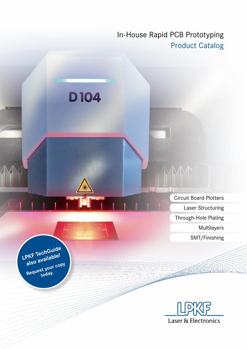
In-House Rapid PCB Prototyping Product Catalog
Circuit Board Plotters
Laser Structuring
Through-Hole Plating
Multilayers
SMT/Finishing
LPKF TechGuide
also available!
Request your copy
today.
Do you have any Questions about your Order? Do you Require Technical Service?
You can find all sales and service contact information below.
Our experienced employees will be happy to assist you.
LPKF AG has a global sales network. An overview of all LPKF representatives can be found on page 40.
For more information, please visit our website at www.lpkf.com.
Germany (LPKF Headquarters)Phone +49 (5131) 7095-0Fax +49 (5131) 7095-90
E-Mail [email protected] [email protected]
Website www.lpkf.com
North/Central AmericaPhone +1 (503) 454-4200Fax +1 (503) 682-7151
E-Mail [email protected] [email protected]
Website www.lpkfusa.com
ChinaPhone Sales +86 (22) 2378-5318 Service +86 (22) 2378-5328Fax +86 (22) 2378-5398
E-Mail [email protected] Website www.lpkf.com
JapanPhone +81 (3) 5439-5906Fax +81 (3) 5439-5908
E-Mail [email protected] Website www.lpkf.com
South KoreaPhone +82 (31) 639 3660Fax +82 (31) 478 5988
E-Mail [email protected] Website www.lpkf.com
LPKF Sales and Service
Worldwide LPKF Representatives
www.lpkf.com/distributor
1
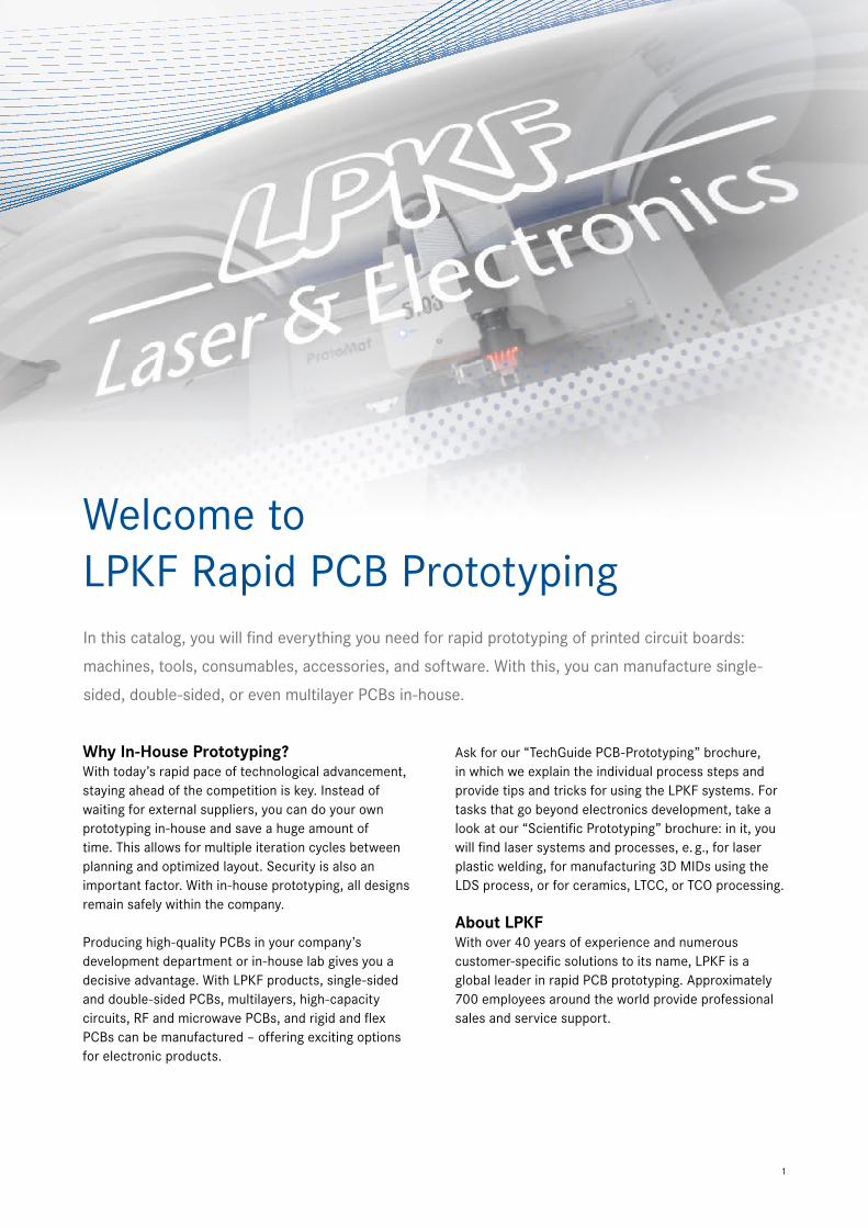
Welcome toLPKF Rapid PCB PrototypingIn this catalog, you will find everything you need for rapid prototyping of printed circuit boards:
machines, tools, consumables, accessories, and software. With this, you can manufacture single-
sided, double-sided, or even multilayer PCBs in-house.
Why In-House Prototyping?With today’s rapid pace of technological advancement, staying ahead of the competition is key. Instead of waiting for external suppliers, you can do your own prototyping in-house and save a huge amount of time. This allows for multiple iteration cycles between planning and optimized layout. Security is also an important factor. With in-house prototyping, all designs remain safely within the company.
Producing high-quality PCBs in your company’s development department or in-house lab gives you a decisive advantage. With LPKF products, single-sided and double-sided PCBs, multilayers, high-capacity circuits, RF and microwave PCBs, and rigid and flex PCBs can be manufactured – offering exciting options for electronic products.
Ask for our “TechGuide PCB-Prototyping” brochure, in which we explain the individual process steps and provide tips and tricks for using the LPKF systems. For tasks that go beyond electronics development, take a look at our “Scientific Prototyping” brochure: in it, you will find laser systems and processes, e. g., for laser plastic welding, for manufacturing 3D MIDs using the LDS process, or for ceramics, LTCC, or TCO processing.
About LPKFWith over 40 years of experience and numerous customer-specific solutions to its name, LPKF is a global leader in rapid PCB prototyping. Approximately 700 employees around the world provide professional sales and service support.
2
Rapid PCB Prototyping – the Faster Way to Create Circuit Boards 3
LPKF Circuit Board Plotters 4Overview of Application Areas 6LPKF ProtoMat E34/E44 – Compact, Easy to Use, Precise 8LPKF ProtoMat S63 – All-Around Talent for Rapid PCB Prototyping 9LPKF ProtoMat S103 – Designed for RF and Microwave Applications 10LPKF ProtoMat D104 – Fine Pitch and Maximum Precision 11Comparison of LPKF Circuit Board Plotters 12
Innovative Laser Technology for Rapid PCB Prototyping 13Laser Micro Material Processing 14LPKF ProtoLaser S4 – Laser Structuring of PCBs 15LPKF ProtoLaser U4 – Multipurpose Tool for the Electronics Lab 16Options and Accessories for LPKF Circuit Board Plotters and ProtoLasers 17Operating Materials for LPKF Circuit Board Plotters and ProtoLasers 19
LPKF Drilling and Milling Tools for LPKF ProtoMats 21
LPKF CircuitPro – Smart Software with Intuitive Operation 23
Systems and Processes for Manufacturing Component Assemblies 25LPKF EasyContac – Manual Through-Hole Plating of Double-Sided PCBs 26LPKF ProConduct – Through-Hole Plating of PCBs with No Chemicals 26LPKF Contac S4 – Table-Top Through-Hole Electroplating 27LPKF MultiPress S – Multilayer Press 28LPKF ProMask and ProLegend – Solder Masks and Legend Printing 29LPKF ProtoPrint S and ProtoPrint S RP – SMT Stencil Printers 30LPKF ProtoPlace S – Easy SMT Assembly 31LPKF ProtoFlow S/N2 – Reflow Ovens for Lead-Free Soldering 32Accessories for SMT Systems and Processes 33
Scientific Prototyping – Laser Systems for Development and Science 36
Conductive Traces on 3D Plastic Parts – LPKF ProtoLaser 3D 37
Micro Material Processing Specialist 38
LPKF International Contacts 40
Legal Information 41
Table of Contents
3
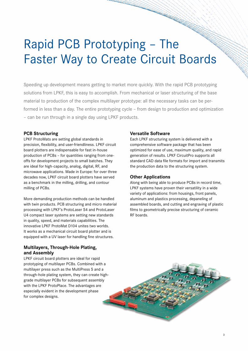
Rapid PCB Prototyping – The Faster Way to Create Circuit Boards
Speeding up development means getting to market more quickly. With the rapid PCB prototyping
solutions from LPKF, this is easy to accomplish. From mechanical or laser structuring of the base
material to production of the complex multilayer prototype: all the necessary tasks can be per-
formed in less than a day. The entire prototyping cycle – from design to production and optimization
– can be run through in a single day using LPKF products.
PCB StructuringLPKF ProtoMats are setting global standards in precision, flexibility, and user-friendliness. LPKF circuit board plotters are indispensable for fast in-house production of PCBs – for quantities ranging from one-offs for development projects to small batches. They are ideal for high-capacity, analog, digital, RF, and microwave applications. Made in Europe: for over three decades now, LPKF circuit board plotters have served as a benchmark in the milling, drilling, and contour milling of PCBs.
More demanding production methods can be handled with twin products. PCB structuring and micro material processing with LPKF’s ProtoLaser S4 and ProtoLaser U4 compact laser systems are setting new standards in quality, speed, and materials capabilities. The innovative LPKF ProtoMat D104 unites two worlds. It works as a mechanical circuit board plotter and is equipped with a UV laser for handling fine structures.
Multilayers, Through-Hole Plating, and AssemblyLPKF circuit board plotters are ideal for rapid prototyping of multilayer PCBs. Combined with a multilayer press such as the MultiPress S and a through-hole plating system, they can create high-grade multilayer PCBs for subsequent assembly with the LPKF ProtoPlace. The advantages are especially evident in the development phase for complex designs.
Versatile SoftwareEach LPKF structuring system is delivered with a comprehensive software package that has been optimized for ease of use, maximum quality, and rapid generation of results. LPKF CircuitPro supports all standard CAD data file formats for import and transmits the production data to the structuring system.
Other ApplicationsAlong with being able to produce PCBs in record time, LPKF systems have proven their versatility in a wide variety of applications: from housings, front panels, aluminum and plastics processing, depaneling of assembled boards, and cutting and engraving of plastic films to geometrically precise structuring of ceramic RF boards.
4
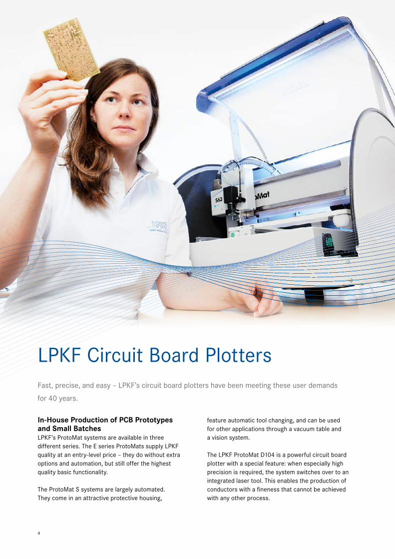
LPKF Circuit Board Plotters
In-House Production of PCB Prototypes and Small BatchesLPKF’s ProtoMat systems are available in three different series. The E series ProtoMats supply LPKF quality at an entry-level price – they do without extra options and automation, but still offer the highest quality basic functionality.
The ProtoMat S systems are largely automated. They come in an attractive protective housing,
feature automatic tool changing, and can be used for other applications through a vacuum table and a vision system.
The LPKF ProtoMat D104 is a powerful circuit board plotter with a special feature: when especially high precision is required, the system switches over to an integrated laser tool. This enables the production of conductors with a fineness that cannot be achieved with any other process.
Fast, precise, and easy – LPKF’s circuit board plotters have been meeting these user demands
for 40 years.
5
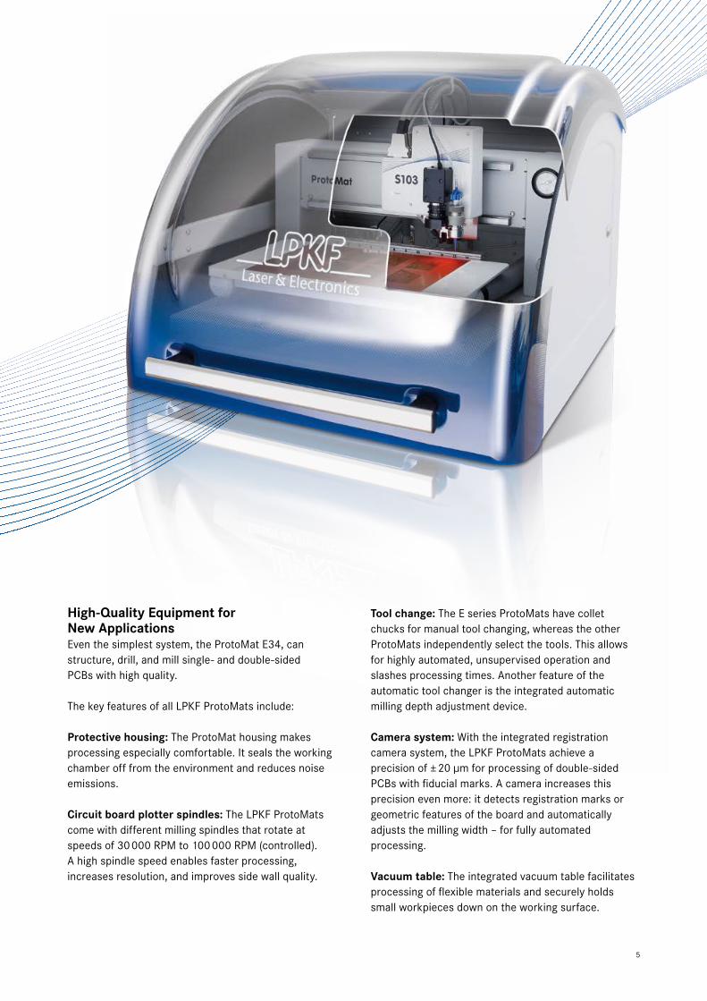
High-Quality Equipment for New ApplicationsEven the simplest system, the ProtoMat E34, can structure, drill, and mill single- and double-sided PCBs with high quality.
The key features of all LPKF ProtoMats include:
Protective housing: The ProtoMat housing makes processing especially comfortable. It seals the working chamber off from the environment and reduces noise emissions.
Circuit board plotter spindles: The LPKF ProtoMats come with different milling spindles that rotate at speeds of 30 000 RPM to 100 000 RPM (controlled). A high spindle speed enables faster processing, increases resolution, and improves side wall quality.
Tool change: The E series ProtoMats have collet chucks for manual tool changing, whereas the other ProtoMats independently select the tools. This allows for highly automated, unsupervised operation and slashes processing times. Another feature of the automatic tool changer is the integrated automatic milling depth adjustment device.
Camera system: With the integrated registration camera system, the LPKF ProtoMats achieve a precision of ± 20 µm for processing of double-sided PCBs with fiducial marks. A camera increases this precision even more: it detects registration marks or geometric features of the board and automatically adjusts the milling width – for fully automated processing.
Vacuum table: The integrated vacuum table facilitates processing of flexible materials and securely holds small workpieces down on the working surface.
6
Milling/Drilling of Single- and Double-Sided PCBsThe main application for LPKF ProtoMats is production of PCB prototypes with FR4 substrates by milling of insulation channels, drilling of mounting and contact holes, and routing of the board out of the base material.
Milling/Drilling of RF and Microwave SubstratesRF and microwave prototypes require extremely precise structuring of special base materials. High-speed spindles produce these fine structures with 90° edges and minimal penetration into the substrate.
Milling/Drilling of Multilayers with up to Eight LayersLPKF processes can be used to manufacture multilayer prototypes with up to eight layers. For this, a fiducial camera is recommended for precise positioning.
Milling of Flexible and Rigid-flex PCBsA vacuum table holds flexible printed circuit board materials securely against the working surface. A high spindle rotational speed aids in gentle structuring and depaneling of these delicate boards.
Contour Milling of PCBsWhen there are multiple PCBs arranged on a base material, routing contours with break-out tabs allow for depaneling without causing damage.
Engraving of Front Panels and LabelsLPKF circuit board plotters can engrave flat front panels and labels made of plastic, Plexiglas, aluminum, brass, and other materials with high precision.
Routing of Cutouts in Front PanelsUnlike engraving, this involves penetration of the material.
Processing of HousingsLPKF circuit board plotters with adjustable Z-axes (maximum travel: 35 mm) can be used to manufacture planar and nonplanar housing parts.
Milling of PlasticsThanks to the 2.5-dimensional capabilities, parts or mounting brackets can be produced from suitable plastic block materials.
Milling of SMT Solder Paste StencilsWith the circuit board plotter, polyimide stencils for solder paste printing can be manufactured directly from CAD data.
Overview of Application Areas
Milling of Solder FramesSolder frames hold the boards in place during the soldering process. LPKF circuit board plotters with stepper motor-controlled Z-axes are ideal for milling of the fixtures in relatively thick temperature-resistant material.
Reworking of PCBsLPKF ProtoMats can be used for the efficient depaneling of assembled (populated) and bare (unpopulated) boards as well as for PCB reworking.
Drilling of Test AdaptersWith an LPKF ProtoMat with high-speed spindle and stepper motor-controlled Z-axis, adapter plates for a bed of nails tester can be drilled perfectly.
Inspection TemplatesLPKF circuit board plotters are ideally suited to precise structuring of inspection templates.
Depaneling of Assembled BoardsCutting of tabs or full-section cuts can be performed as long as the cutting channel can be accessed by the ProtoMat’s tool.
Ultrafine Conductor StructuringFor high-resolution, highly integrated electronic components, a large number of densely packed connector terminals must be contacted. The very fine (< 200 µm) conductor structures require high spindle speeds or laser tools.
Metal Layers on CeramicsMetal layers on fired ceramics are sensitive to mechanical loads, but they also place high demands on the tools. This is where the laser shines because it works without exerting any mechanical forces.
Reworking of RF StructuresThe LPKF ProtoMat D104 can rapidly produce rough structures and add the finishing touches with the laser tool, e. g., for complex RF structures.
DispensingThe compressed air-assisted dispenser applies the solder paste to the board with high positioning accuracy.
7
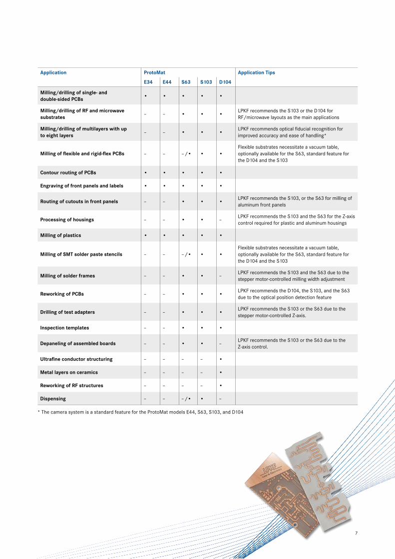
Application ProtoMat Application Tips
E34 E44 S63 S103 D104
Milling/drilling of single- and double-sided PCBs
• • • • •
Milling/drilling of RF and microwave substrates
– – • • •LPKF recommends the S103 or the D104 for RF/microwave layouts as the main applications
Milling/drilling of multilayers with up to eight layers
– – • • •LPKF recommends optical fiducial recognition for improved accuracy and ease of handling*
Milling of flexible and rigid-flex PCBs – – – /• • •Flexible substrates necessitate a vacuum table, optionally available for the S63, standard feature for the D104 and the S103
Contour routing of PCBs • • • • •
Engraving of front panels and labels • • • • •
Routing of cutouts in front panels – – • • •LPKF recommends the S103, or the S63 for milling of aluminum front panels
Processing of housings – – • • –LPKF recommends the S103 and the S63 for the Z-axis control required for plastic and aluminum housings
Milling of plastics • • • • •
Milling of SMT solder paste stencils – – – /• • •Flexible substrates necessitate a vacuum table, optionally available for the S63, standard feature for the D104 and the S103
Milling of solder frames – – • • –LPKF recommends the S103 and the S63 due to the stepper motor-controlled milling width adjustment
Reworking of PCBs – – • • •LPKF recommends the D104, the S103, and the S63 due to the optical position detection feature
Drilling of test adapters – – • • •LPKF recommends the S103 or the S63 due to the stepper motor-controlled Z-axis.
Inspection templates – – • • •
Depaneling of assembled boards – – • • –LPKF recommends the S103 or the S63 due to the Z-axis control.
Ultrafine conductor structuring – – – – •
Metal layers on ceramics – – – – •
Reworking of RF structures – – – – •
Dispensing – – – /• • –
* The camera system is a standard feature for the ProtoMat models E44, S63, S103, and D104
8
• Table system barely larger than a DIN A3 sheet
• Speed of 30 000 or 40 000 RPM• Manual tool exchange• With LPKF CircuitPro software• LPKF quality at an entry-level price
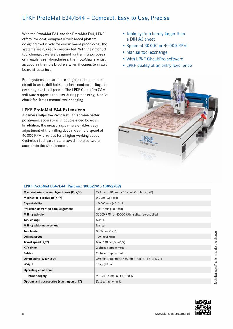
LPKF ProtoMat E34/E44 – Compact, Easy to Use, Precise
With the ProtoMat E34 and the ProtoMat E44, LPKF offers low-cost, compact circuit board plotters designed exclusively for circuit board processing. The systems are ruggedly constructed. With their manual tool change, they are designed for training purposes or irregular use. Nonetheless, the ProtoMats are just as good as their big brothers when it comes to circuit board structuring.
Both systems can structure single- or double-sided circuit boards, drill holes, perform contour milling, and even engrave front panels. The LPKF CircuitPro CAM software supports the user during processing. A collet chuck facilitates manual tool changing.
LPKF ProtoMat E44 ExtensionsA camera helps the ProtoMat E44 achieve better positioning accuracy with double-sided boards. In addition, the measuring camera enables easy adjustment of the milling depth. A spindle speed of 40 000 RPM provides for a higher working speed. Optimized tool parameters saved in the software accelerate the work process.
LPKF ProtoMat E34/E44 (Part no.: 10052741 /10052739)
Max. material size and layout area (X/Y/Z) 229 mm x 305 mm x 10 mm (9” x 12” x 0.4”)
Mechanical resolution (X/Y) 0.8 µm (0.04 mil)
Repeatability ± 0.005 mm (± 0.2 mil)
Precision of front-to-back alignment ± 0.02 mm (± 0.8 mil)
Milling spindle 30 000 RPM or 40 000 RPM, software-controlled
Tool change Manual
Milling width adjustment Manual
Tool holder 3.175 mm (1/8”)
Drilling speed 100 holes/min
Travel speed (X/Y) Max. 100 mm/s (4”/s)
X/Y-drive 2-phase stepper motor
Z-drive 2-phase stepper motor
Dimensions (W x H x D) 370 mm x 300 mm x 450 mm (14.6” x 11.8” x 17.7”)
Weight 15 kg (33 lbs)
Operating conditions
Power supply 90 – 240 V, 50 – 60 Hz, 120 W
Options and accessories (starting on p. 17) Dust extraction unit Tech
nica
l spe
cific
atio
ns s
ubje
ct to
cha
nge.
www.lpkf.com/protomat-e44
9
• Fully automated operation• High speed (60 000 RPM), mechanical
resolution, and repeatability• Automatic tool change (15 positions)
and milling depth adjustment• Optical fiducial recognition
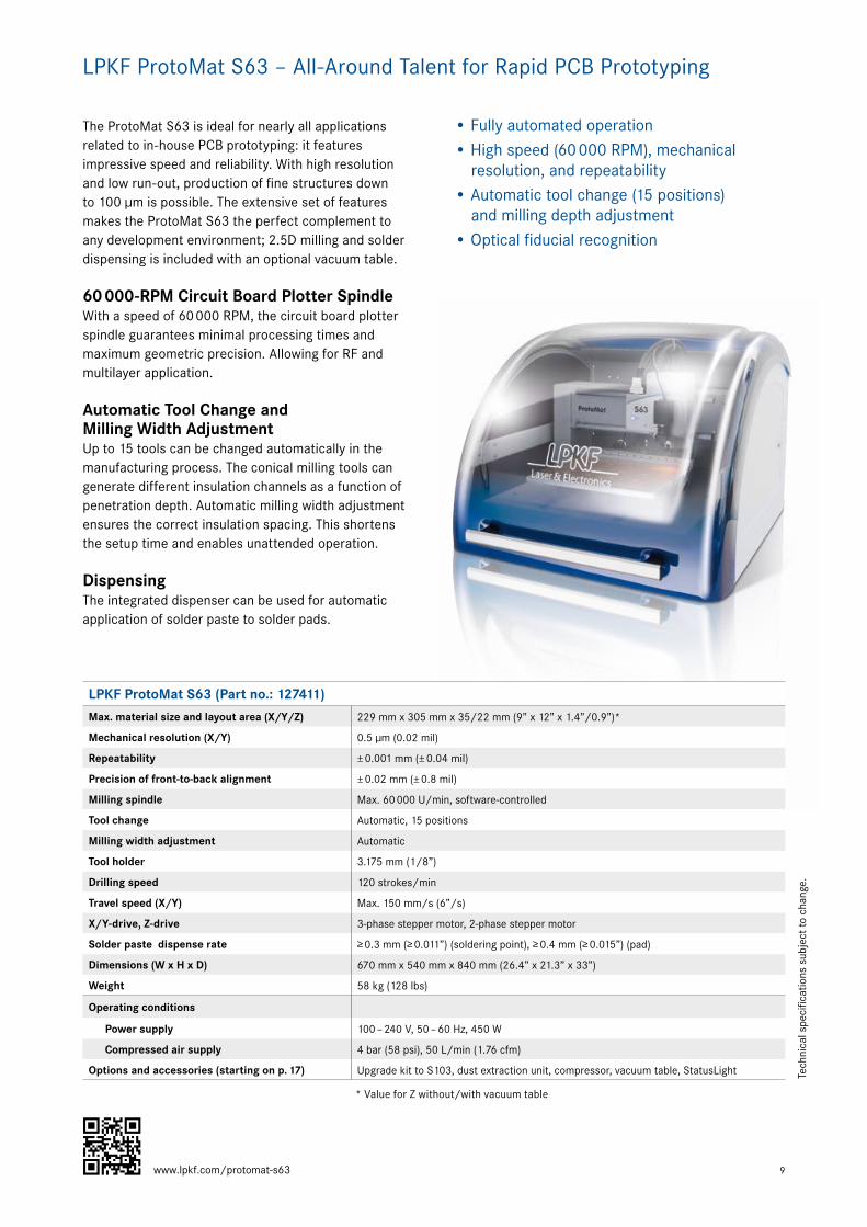
LPKF ProtoMat S63 – All-Around Talent for Rapid PCB Prototyping
The ProtoMat S63 is ideal for nearly all applications related to in-house PCB prototyping: it features impressive speed and reliability. With high resolution and low run-out, production of fine structures down to 100 µm is possible. The extensive set of features makes the ProtoMat S63 the perfect complement to any development environment; 2.5D milling and solder dispensing is included with an optional vacuum table.
60 000-RPM Circuit Board Plotter SpindleWith a speed of 60 000 RPM, the circuit board plotter spindle guarantees minimal processing times and maximum geometric precision. Allowing for RF and multilayer application.
Automatic Tool Change and Milling Width AdjustmentUp to 15 tools can be changed automatically in the manufacturing process. The conical milling tools can generate different insulation channels as a function of penetration depth. Automatic milling width adjustment ensures the correct insulation spacing. This shortens the setup time and enables unattended operation.
DispensingThe integrated dispenser can be used for automatic application of solder paste to solder pads.
Tech
nica
l spe
cific
atio
ns s
ubje
ct to
cha
nge.
www.lpkf.com/protomat-s63
LPKF ProtoMat S63 (Part no.: 127411)
Max. material size and layout area (X/Y/Z) 229 mm x 305 mm x 35/22 mm (9” x 12” x 1.4”/0.9”)*
Mechanical resolution (X/Y) 0.5 µm (0.02 mil)
Repeatability ± 0.001 mm (± 0.04 mil)
Precision of front-to-back alignment ± 0.02 mm (± 0.8 mil)
Milling spindle Max. 60 000 U/min, software-controlled
Tool change Automatic, 15 positions
Milling width adjustment Automatic
Tool holder 3.175 mm (1/8”)
Drilling speed 120 strokes/min
Travel speed (X/Y) Max. 150 mm/s (6”/s)
X/Y-drive, Z-drive 3-phase stepper motor, 2-phase stepper motor
Solder paste dispense rate ≥ 0.3 mm (≥ 0.011”) (soldering point), ≥ 0.4 mm (≥ 0.015”) (pad)
Dimensions (W x H x D) 670 mm x 540 mm x 840 mm (26.4” x 21.3” x 33”)
Weight 58 kg (128 lbs)
Operating conditions
Power supply 100 – 240 V, 50 – 60 Hz, 450 W
Compressed air supply 4 bar (58 psi), 50 L/min (1.76 cfm)
Options and accessories (starting on p. 17) Upgrade kit to S103, dust extraction unit, compressor, vacuum table, StatusLight
* Value for Z without/with vacuum table
10
LPKF ProtoMat S103 – Designed for RF and Microwave Applications
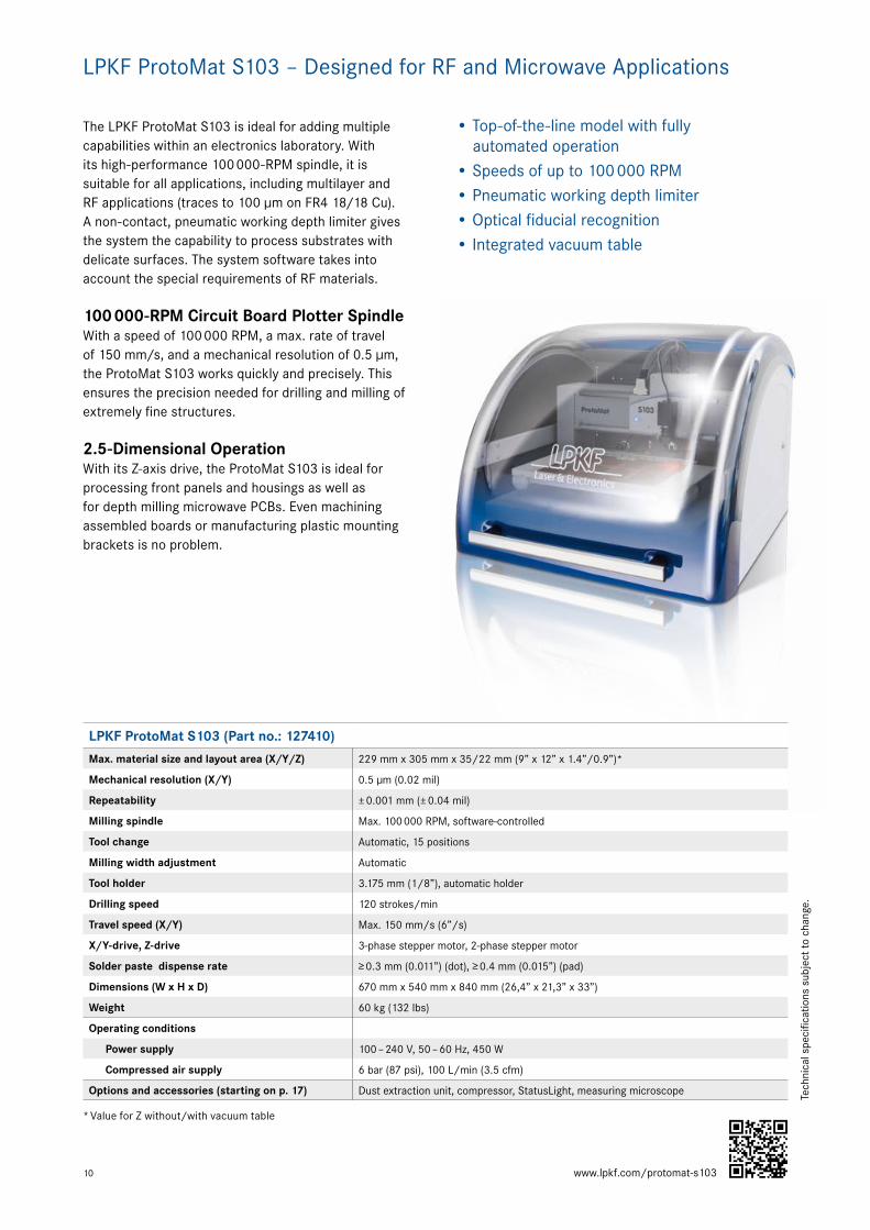
The LPKF ProtoMat S103 is ideal for adding multiple capabilities within an electronics laboratory. With its high-performance 100 000-RPM spindle, it is suitable for all applications, including multilayer and RF applications (traces to 100 µm on FR4 18/18 Cu). A non-contact, pneumatic working depth limiter gives the system the capability to process substrates with delicate surfaces. The system software takes into account the special requirements of RF materials.
100 000-RPM Circuit Board Plotter SpindleWith a speed of 100 000 RPM, a max. rate of travel of 150 mm/s, and a mechanical resolution of 0.5 µm, the ProtoMat S103 works quickly and precisely. This ensures the precision needed for drilling and milling of extremely fine structures.
2.5-Dimensional OperationWith its Z-axis drive, the ProtoMat S103 is ideal for processing front panels and housings as well as for depth milling microwave PCBs. Even machining assembled boards or manufacturing plastic mounting brackets is no problem.
LPKF ProtoMat S103 (Part no.: 127410)
Max. material size and layout area (X/Y/Z) 229 mm x 305 mm x 35/22 mm (9” x 12” x 1.4”/0.9”)*
Mechanical resolution (X/Y) 0.5 µm (0.02 mil)
Repeatability ± 0.001 mm (± 0.04 mil)
Milling spindle Max. 100 000 RPM, software-controlled
Tool change Automatic, 15 positions
Milling width adjustment Automatic
Tool holder 3.175 mm (1/8”), automatic holder
Drilling speed 120 strokes/min
Travel speed (X/Y) Max. 150 mm/s (6”/s)
X/Y-drive, Z-drive 3-phase stepper motor, 2-phase stepper motor
Solder paste dispense rate ≥ 0.3 mm (0.011”) (dot), ≥ 0.4 mm (0.015”) (pad)
Dimensions (W x H x D) 670 mm x 540 mm x 840 mm (26,4” x 21,3” x 33”)
Weight 60 kg (132 lbs)
Operating conditions
Power supply 100 – 240 V, 50 – 60 Hz, 450 W
Compressed air supply 6 bar (87 psi), 100 L/min (3.5 cfm)
Options and accessories (starting on p. 17) Dust extraction unit, compressor, StatusLight, measuring microscope
* Value for Z without/with vacuum table
• Top-of-the-line model with fully automated operation
• Speeds of up to 100 000 RPM• Pneumatic working depth limiter• Optical fiducial recognition• Integrated vacuum table
www.lpkf.com/protomat-s103
Tech
nica
l spe
cific
atio
ns s
ubje
ct to
cha
nge.
11
LPKF ProtoMat D104 (Part no.: 127411)
Max. material size and layout area (X/Y/Z) 305 mm x 229 mm x 10 mm (12” x 9” x 0.4”)
Mechanical resolution (X/Y) 0.3 µm (0.01 mil)
Repeatability ± 1 µm (± 0.04 mil)
Milling spindle Max. 100 000 RPM, software-controlled
Tool change Automatic, 15 positions
Milling width adjustment Automatic
Tool holder 3.175 mm (1/8”)
Drilling speed 120 strokes/min
Travel speed (X/Y) Max. 100 mm/s (3.7”/s)
X/Y-drive, Z-drive 3-phase stepper motor
Solder paste dispense rate 2-phase stepper motor
Dimensions (W x H x D) 660 mm x 700 mm x 870 mm (26” x 27.6” x 34.3”)
Weight 99 kg (218.3 lbs)
Operating conditions
Power supply 85/260 V, 50 – 60 Hz, 440 W
Compressed air supply 6 bar (87 psi), 100 L/min (3.5 cfm)
Options and accessories (starting on p. 17) Dust extraction unit, compressor, StatusLight, measuring microscope
• UV laser tool for high-precision structuring• Integrated measuring camera/vision system• 100 000-RPM spindle, automatic tool
change, vacuum table• Mechanical milling/drilling and laser
structuring
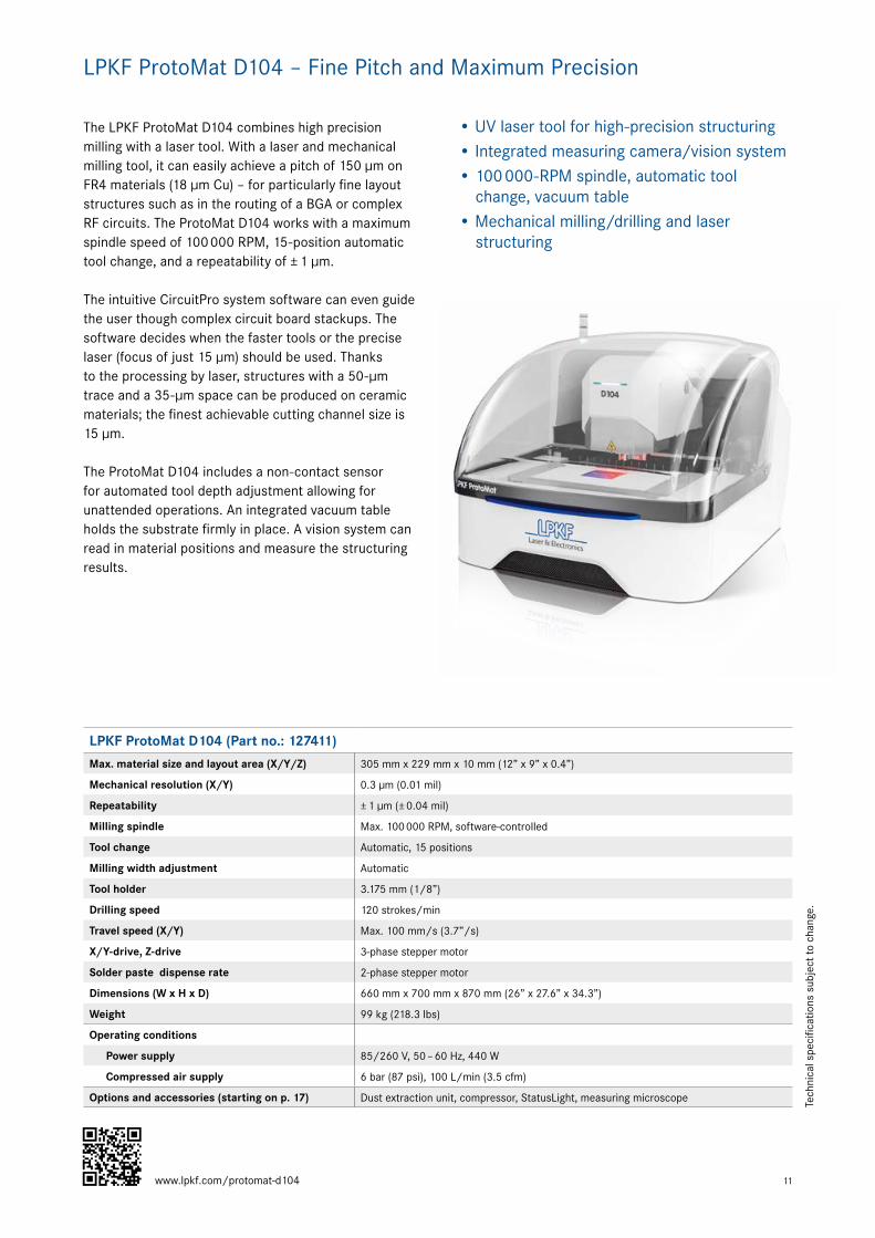
LPKF ProtoMat D104 – Fine Pitch and Maximum Precision
The LPKF ProtoMat D104 combines high precision milling with a laser tool. With a laser and mechanical milling tool, it can easily achieve a pitch of 150 µm on FR4 materials (18 µm Cu) – for particularly fine layout structures such as in the routing of a BGA or complex RF circuits. The ProtoMat D104 works with a maximum spindle speed of 100 000 RPM, 15-position automatic tool change, and a repeatability of ± 1 µm.
The intuitive CircuitPro system software can even guide the user though complex circuit board stackups. The software decides when the faster tools or the precise laser (focus of just 15 µm) should be used. Thanks to the processing by laser, structures with a 50-µm trace and a 35-µm space can be produced on ceramic materials; the finest achievable cutting channel size is 15 µm.
The ProtoMat D104 includes a non-contact sensor for automated tool depth adjustment allowing for unattended operations. An integrated vacuum table holds the substrate firmly in place. A vision system can read in material positions and measure the structuring results.
www.lpkf.com/protomat-d104
Tech
nica
l spe
cific
atio
ns s
ubje
ct to
cha
nge.
12
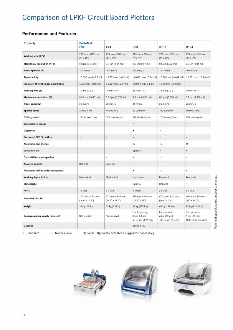
Comparison of LPKF Circuit Board Plotters
Property ProtoMat E34 E44 S63 S103 D104
Working area (X/Y)229 mm x 305 mm
(9” x 12”)
229 mm x 305 mm
(9” x 12”)
229 mm x 305 mm
(9” x 12”)
229 mm x 305 mm
(9” x 12”)
229 mm x 305 mm
(9” x 12”)
Mechanical resolution (X/Y) 0.8 µm (0.04 mil) 0.8 µm (0.04 mil) 0.5 µm (0.02 mil) 0.5 µm (0.02 mil) 0.3 µm (0.01 mil)
Travel speed (X/Y) 100 mm/s 100 mm/s 150 mm/s 150 mm/s 100 mm/s
Repeatability ± 0.005 mm (± 0.2 mil) ± 0.005 mm (± 0.2 mil) ± 0.001 mm (± 0.04 mil) ± 0.001 mm (± 0.04 mil) ± 0.001 mm (± 0.04 mil)
Precision of front-to-back alignment ± 0.02 mm (± 0.8 mil) ± 0.02 mm (± 0.8 mil) ± 0.02 mm (± 0.8 mil) ± 0.02 mm (± 0.8 mil) –
Working area (Z) 10 mm (0.4”) 10 mm (0.4”) 35 mm (1.4”) 22 mm (0.9”) 10 mm (0.4”)
Mechanical resolution (Z) 0.85 µm (0.033 mil) 0.85 µm (0.033 mil) 0.2 µm (0.008 mil) 0.2 µm (0.008 mil) 0.2 µm (0.008 mil)
Travel speed (Z) 20 mm/s 20 mm/s 25 mm/s 25 mm/s 25 mm/s
Spindle speed 30 000 RPM 40 000 RPM 60 000 RPM 100 000 RPM 100 000 RPM
Drilling speed 100 strokes/min 100 strokes/min 120 strokes/min 120 strokes/min 120 strokes/min
Temperature sensor – – • • •
Dispenser – – • • –
Software LPKF CircuitPro • • • • •
Automatic tool change – – 15 15 15
Vacuum table – – Optional • •
Optical fiducial recognition – • • • •
Acoustic cabinet Optional Optional • • •
Automatic milling width adjustment – – • • •
Working depth limiter Mechanical Mechanical Mechanical Pneumatic Pneumatic
StatusLight – – Optional Optional •
Ports 1 x USB 2 x USB 2 x USB 2 x USB 2 x USB
Footprint (W x D)370 mm x 450 mm
(14.6” x 17.7”)
370 mm x 450 mm
(14.6” x 17.7”)
670 mm x 840 mm
(26.4” x 33”)
670 mm x 840 mm
(26.4” x 33”)
660 mm x 870 mm
(26” x 34.3”)
Weight 15 kg (33 lbs) 15 kg (33 lbs) 58 kg (127 lbs) 60 kg (132 lbs) 99 kg (218.3 lbs)
Compressed air supply required? Not required Not required
For dispensing
4 bar (58 psi)
50 L/min (1.76 cfm)
For operation
6 bar (87 psi)
100 L/min (3.5 cfm)
For operation
6 bar (87 psi)
100 L/min (3.5 cfm)
Upgrade – – S63 to S103 – –
Performance and Features
• = Standard – = Not available Optional = Optionally available as upgrade or accessory
Tech
nica
l spe
cific
atio
ns s
ubje
ct to
cha
nge.
13
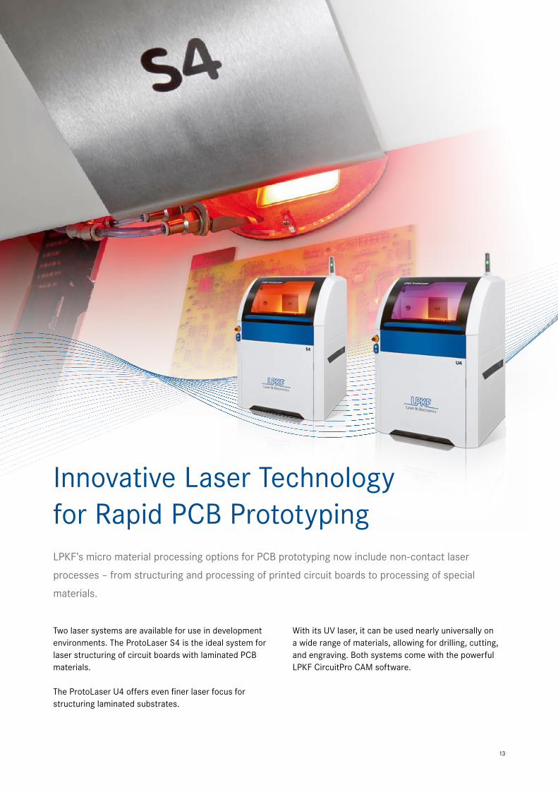
Two laser systems are available for use in development environments. The ProtoLaser S4 is the ideal system for laser structuring of circuit boards with laminated PCB materials.
The ProtoLaser U4 offers even finer laser focus for structuring laminated substrates.
LPKF’s micro material processing options for PCB prototyping now include non-contact laser
processes – from structuring and processing of printed circuit boards to processing of special
materials.
With its UV laser, it can be used nearly universally on a wide range of materials, allowing for drilling, cutting, and engraving. Both systems come with the powerful LPKF CircuitPro CAM software.
Innovative Laser Technology for Rapid PCB Prototyping
14
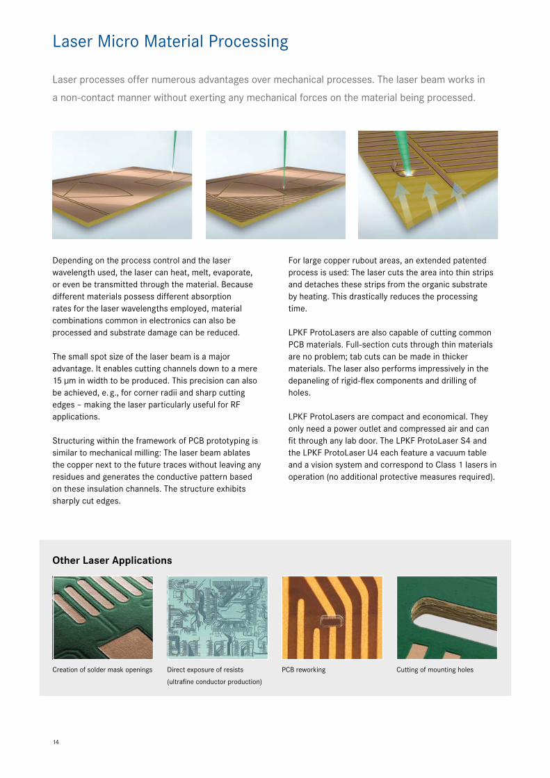
Laser processes offer numerous advantages over mechanical processes. The laser beam works in
a non-contact manner without exerting any mechanical forces on the material being processed.
Laser Micro Material Processing
Depending on the process control and the laser wavelength used, the laser can heat, melt, evaporate, or even be transmitted through the material. Because different materials possess different absorption rates for the laser wavelengths employed, material combinations common in electronics can also be processed and substrate damage can be reduced.
The small spot size of the laser beam is a major advantage. It enables cutting channels down to a mere 15 µm in width to be produced. This precision can also be achieved, e. g., for corner radii and sharp cutting edges – making the laser particularly useful for RF applications.
Structuring within the framework of PCB prototyping is similar to mechanical milling: The laser beam ablates the copper next to the future traces without leaving any residues and generates the conductive pattern based on these insulation channels. The structure exhibits sharply cut edges.
For large copper rubout areas, an extended patented process is used: The laser cuts the area into thin strips and detaches these strips from the organic substrate by heating. This drastically reduces the processing time.
LPKF ProtoLasers are also capable of cutting common PCB materials. Full-section cuts through thin materials are no problem; tab cuts can be made in thicker materials. The laser also performs impressively in the depaneling of rigid-flex components and drilling of holes.
LPKF ProtoLasers are compact and economical. They only need a power outlet and compressed air and can fit through any lab door. The LPKF ProtoLaser S4 and the LPKF ProtoLaser U4 each feature a vacuum table and a vision system and correspond to Class 1 lasers in operation (no additional protective measures required).
Other Laser Applications
Creation of solder mask openings Direct exposure of resists
(ultrafine conductor production)
PCB reworking Cutting of mounting holes
15
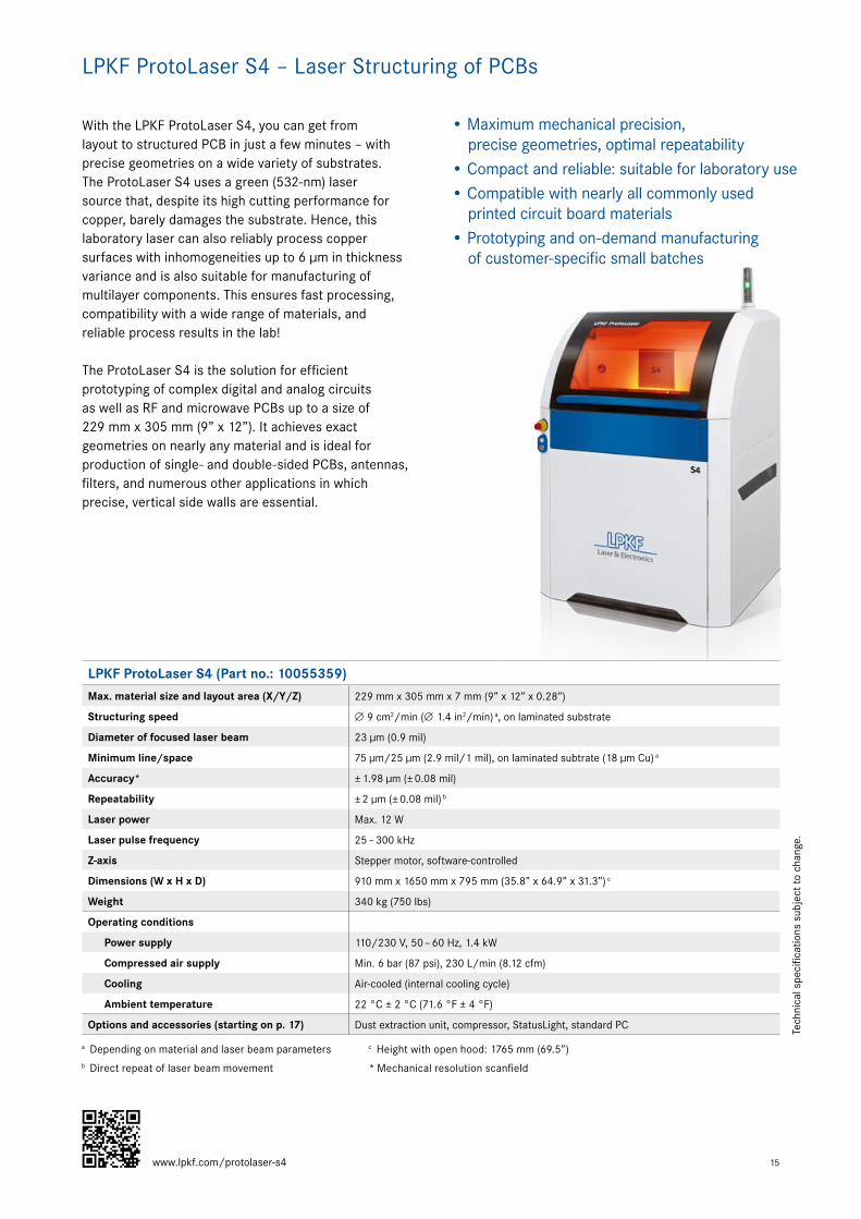
• Maximum mechanical precision, precise geometries, optimal repeatability
• Compact and reliable: suitable for laboratory use• Compatible with nearly all commonly used
printed circuit board materials• Prototyping and on-demand manufacturing
of customer-specific small batches
LPKF ProtoLaser S4 – Laser Structuring of PCBs
With the LPKF ProtoLaser S4, you can get from layout to structured PCB in just a few minutes – with precise geometries on a wide variety of substrates. The ProtoLaser S4 uses a green (532-nm) laser source that, despite its high cutting performance for copper, barely damages the substrate. Hence, this laboratory laser can also reliably process copper surfaces with inhomogeneities up to 6 µm in thickness variance and is also suitable for manufacturing of multilayer components. This ensures fast processing, compatibility with a wide range of materials, and reliable process results in the lab!
The ProtoLaser S4 is the solution for efficient prototyping of complex digital and analog circuits as well as RF and microwave PCBs up to a size of 229 mm x 305 mm (9” x 12”). It achieves exact geometries on nearly any material and is ideal for production of single- and double-sided PCBs, antennas, filters, and numerous other applications in which precise, vertical side walls are essential.
LPKF ProtoLaser S4 (Part no.: 10055359)
Max. material size and layout area (X/Y/Z) 229 mm x 305 mm x 7 mm (9” x 12” x 0.28”)
Structuring speed ∅ 9 cm2/min (∅ 1.4 in2/min) a, on laminated substrate
Diameter of focused laser beam 23 µm (0.9 mil)
Minimum line/space 75 µm/25 µm (2.9 mil/1 mil), on laminated subtrate (18 µm Cu) a
Accuracy* ± 1.98 µm (± 0.08 mil)
Repeatability ± 2 µm (± 0.08 mil) b
Laser power Max. 12 W
Laser pulse frequency 25 – 300 kHz
Z-axis Stepper motor, software-controlled
Dimensions (W x H x D) 910 mm x 1650 mm x 795 mm (35.8” x 64.9” x 31.3”) c
Weight 340 kg (750 lbs)
Operating conditions
Power supply 110/230 V, 50 – 60 Hz, 1.4 kW
Compressed air supply Min. 6 bar (87 psi), 230 L/min (8.12 cfm)
Cooling Air-cooled (internal cooling cycle)
Ambient temperature 22 °C ± 2 °C (71.6 °F ± 4 °F)
Options and accessories (starting on p. 17) Dust extraction unit, compressor, StatusLight, standard PC
a Depending on material and laser beam parametersb Direct repeat of laser beam movement
c Height with open hood: 1765 mm (69.5”)
* Mechanical resolution scanfield
www.lpkf.com/protolaser-s4
Tech
nica
l spe
cific
atio
ns s
ubje
ct to
cha
nge.
16
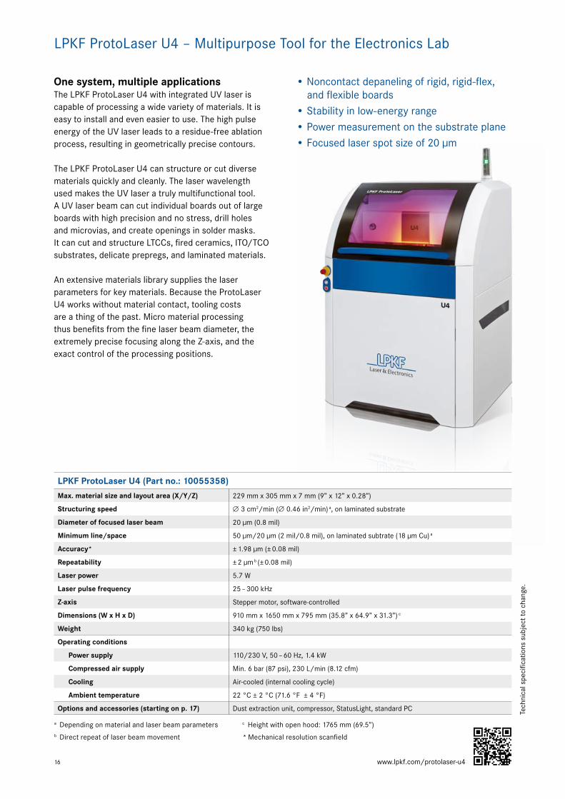
• Noncontact depaneling of rigid, rigid-flex, and flexible boards
• Stability in low-energy range• Power measurement on the substrate plane• Focused laser spot size of 20 µm
LPKF ProtoLaser U4 – Multipurpose Tool for the Electronics Lab
One system, multiple applicationsThe LPKF ProtoLaser U4 with integrated UV laser is capable of processing a wide variety of materials. It is easy to install and even easier to use. The high pulse energy of the UV laser leads to a residue-free ablation process, resulting in geometrically precise contours.
The LPKF ProtoLaser U4 can structure or cut diverse materials quickly and cleanly. The laser wavelength used makes the UV laser a truly multifunctional tool. A UV laser beam can cut individual boards out of large boards with high precision and no stress, drill holes and microvias, and create openings in solder masks. It can cut and structure LTCCs, fired ceramics, ITO/TCO substrates, delicate prepregs, and laminated materials.
An extensive materials library supplies the laser parameters for key materials. Because the ProtoLaser U4 works without material contact, tooling costs are a thing of the past. Micro material processing thus benefits from the fine laser beam diameter, the extremely precise focusing along the Z-axis, and the exact control of the processing positions.
LPKF ProtoLaser U4 (Part no.: 10055358)
Max. material size and layout area (X/Y/Z) 229 mm x 305 mm x 7 mm (9” x 12” x 0.28”)
Structuring speed ∅ 3 cm2/min (∅ 0.46 in2/min) a, on laminated substrate
Diameter of focused laser beam 20 µm (0.8 mil)
Minimum line/space 50 µm/20 µm (2 mil/0.8 mil), on laminated subtrate (18 µm Cu) a
Accuracy* ± 1.98 µm (± 0.08 mil)
Repeatability ± 2 µm b (± 0.08 mil)
Laser power 5.7 W
Laser pulse frequency 25 – 300 kHz
Z-axis Stepper motor, software-controlled
Dimensions (W x H x D) 910 mm x 1650 mm x 795 mm (35.8” x 64.9” x 31.3”) c
Weight 340 kg (750 lbs)
Operating conditions
Power supply 110/230 V, 50 – 60 Hz, 1.4 kW
Compressed air supply Min. 6 bar (87 psi), 230 L/min (8.12 cfm)
Cooling Air-cooled (internal cooling cycle)
Ambient temperature 22 °C ± 2 °C (71.6 °F ± 4 °F)
Options and accessories (starting on p. 17) Dust extraction unit, compressor, StatusLight, standard PC
a Depending on material and laser beam parametersb Direct repeat of laser beam movement
c Height with open hood: 1765 mm (69.5”)
* Mechanical resolution scanfield
www.lpkf.com/protolaser-u4
Tech
nica
l spe
cific
atio
ns s
ubje
ct to
cha
nge.
17Technical specifications subject to change.
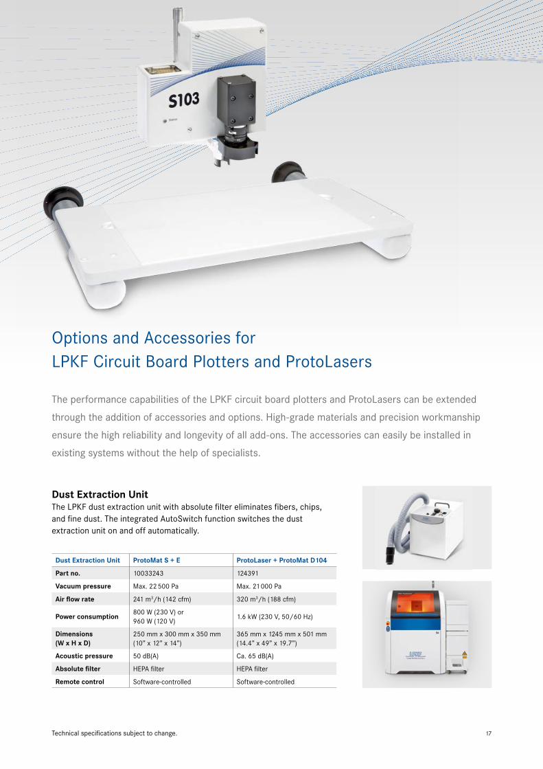
The performance capabilities of the LPKF circuit board plotters and ProtoLasers can be extended
through the addition of accessories and options. High-grade materials and precision workmanship
ensure the high reliability and longevity of all add-ons. The accessories can easily be installed in
existing systems without the help of specialists.
Options and Accessories for LPKF Circuit Board Plotters and ProtoLasers
Dust Extraction UnitThe LPKF dust extraction unit with absolute filter eliminates fibers, chips, and fine dust. The integrated AutoSwitch function switches the dust extraction unit on and off automatically.
Dust Extraction Unit ProtoMat S + E ProtoLaser + ProtoMat D104
Part no. 10033243 124391
Vacuum pressure Max. 22 500 Pa Max. 21 000 Pa
Air flow rate 241 m3/h (142 cfm) 320 m3/h (188 cfm)
Power consumption800 W (230 V) or 960 W (120 V)
1.6 kW (230 V, 50/60 Hz)
Dimensions (W x H x D)
250 mm x 300 mm x 350 mm (10” x 12” x 14”)
365 mm x 1245 mm x 501 mm(14.4” x 49” x 19.7”)
Acoustic pressure 50 dB(A) Ca. 65 dB(A)
Absolute filter HEPA filter HEPA filter
Remote control Software-controlled Software-controlled
18 Technical specifications subject to change.
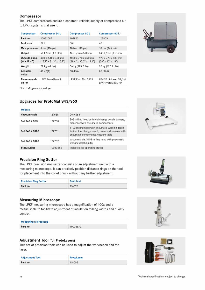
Upgrades for ProtoMat S43/S63
Module Part no. Beschreibung
Vacuum table 127688 Only S63
Set S43 > S63 127700S63 milling head with tool change bench, camera, dispenser with pneumatic components
Set S43 > S103 127701S103 milling head with pneumatic working depth limiter, tool change bench, camera, dispenser with pneumatic components, vacuum table
Set S63 > S103 127702Vacuum table, S103 milling head with pneumatic working depth limiter
StatusLight 10023555 Indicates the operating status
Measuring MicroscopeThe LPKF measuring microscope has a magnification of 100x and a metric scale to facilitate adjustment of insulation milling widths and quality control.
Measuring Microscope
Part no. 10035579
Precision Ring SetterThe LPKF precision ring setter consists of an adjustment unit with a measuring microscope. It can precisely position distance rings on the tool for placement into the collet chuck without any further adjustment.
Precision Ring Setter ProtoMat
Part no. 116698
Adjustment Tool (for ProtoLasers)This set of precision tools can be used to adjust the workbench and the laser.
Adjustment Tool ProtoLaser
Part no. 118005
CompressorThe LPKF compressors ensure a constant, reliable supply of compressed airto LPKF systems that use it.
Compressor Compressor 24 L Compressor 50 L Compressor 60 L*
Part no. 10032687 104863 122805
Tank size 24 L 50 L 60 L
Max. pressure 8 bar (116 psi) 10 bar (145 psi) 10 bar (145 psi)
Output 50 L/min (1.8 cfm) 165 L/min (5.8 cfm) 240 L/min (8.5 cfm)
Outside dims. (W x H x D)
400 x 540 x 400 mm(15.7” x 21.3” x 15.7”)
1000 x 770 x 390 mm(39.4” x 30.3” x 15.4”)
970 x 770 x 480 mm(38” x 30” x 19”)
Weight 29 kg (64 lbs) 56 kg (123.2 lbs) 90 kg (198.4 lbs)
Acoustic noise
40 dB(A) 68 dB(A) 83 dB(A)
Recommend-ed for
LPKF ProtoPlace S LPKF ProtoMat S103 LPKF ProtoLaser S4/U4LPKF ProtoMat D104
* incl. refrigerant-type dryer
19Technical specifications subject to change.
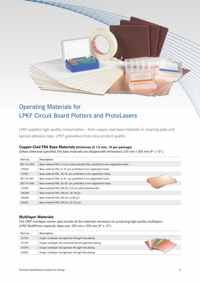
LPKF supplies high-quality consumables – from copper-clad base materials to cleaning pads and
special adhesive tape, LPKF guarantees first-class product quality.
Copper-Clad FR4 Base Materials (thickness of 1.5 mm, 10 per package)Unless otherwise specified, the base materials are shipped with dimensions 229 mm x 305 mm (9” x 12”).
Part no. Description
SET-10-1053 Base material FR4, 5/5 µm with protective film, predrilled 3-mm registration holes
115968 Base material FR4, 0/18 µm, predrilled 3-mm registration holes
115967 Base material FR4, 18/18 µm, predrilled 3-mm registration holes
SET-10-1001 Base material FR4, 0/35 µm, predrilled 3-mm registration holes
SET-10-1000 Base material FR4, 35/35 µm, predrilled 3-mm registration holes
112059 Base material FR4, DIN A3, 5/5 µm with protective film
106398 Base material FR4, DIN A3, 18/18 µm
106400 Base material FR4, DIN A3, 0/35 µm
106401 Base material FR4, DIN A3, 35/35 µm
Multilayer MaterialsThe LPKF multilayer starter sets include all the materials necessary for producing high-quality multilayers (LPKF MultiPress required). Base size: 229 mm x 305 mm (9” x 12”).
Part no. Description
121103 4-layer multilayer set/galvanic through-hole plating
121102 4-layer multilayer set/chemical-free through-hole plating
121093 6-layer multilayer set/galvanic through-hole plating
124481 8-layer multilayer set/galvanic through-hole plating
Operating Materials for LPKF Circuit Board Plotters and ProtoLasers
20
Part no. Description
127696 Starter set for ProtoMat E34/E44
115791 Starter set for ProtoMat S63, without vacuum table
122157 Starter set for ProtoMat S63, with vacuum table
122159 Starter set for ProtoMat S103
10035172 Starter set for ProtoMat D104
Cleaning Pads
Part no. Description Pads per Package
106403 The metal-free, ultrafine board cleaning pads remove the oxidation residues from the copper layer on the base material.
10
Special Adhesive Tape
Part no. Description
106373 The special adhesive tape holds the base material flat against the workbench and can be removed without leaving any residues.
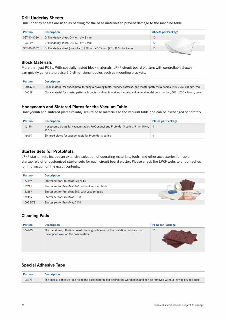
Starter Sets for ProtoMatsLPKF starter sets include an extensive selection of operating materials, tools, and other accessories for rapid startup. We offer customized starter sets for each circuit board plotter. Please check the LPKF website or contact us for information on the exact contents.
Honeycomb and Sintered Plates for the Vacuum TableHoneycomb and sintered plates reliably secure base materials to the vacuum table and can be exchanged separately.
Part no. Description Plates per Package
116148 Honeycomb plates for vacuum tables ProConduct and ProtoMat S series, 5 mm thick, ∅ 3.5 mm
4
116099 Sintered plates for vacuum table for ProtoMat S series 4
Drill Underlay SheetsDrill underlay sheets are used as backing for the base materials to prevent damage to the machine table.
Block MaterialsMore than just PCBs. With specially tested block materials, LPKF circuit board plotters with controllable Z-axes can quickly generate precise 2.5-dimensional bodies such as mounting brackets.
Part no. Description Sheets per Package
SET-10-1086 Drill underlay sheet, DIN A4, d = 2 mm 10
106389 Drill underlay sheet, DIN A3, d = 2 mm 10
SET-10-1052 Drill underlay sheet (predrilled), 229 mm x 305 mm (9” x 12”), d = 2 mm 10
Part no. Description
10044715 Block material for sheet metal forming & drawing tools, foundry patterns, and master patterns & copies, 250 x 250 x 8 mm, red
106389 Block material for master patterns & copies, cubing & working models, and general model construction, 300 x 250 x 8 mm, brown
Technical specifications subject to change.
21
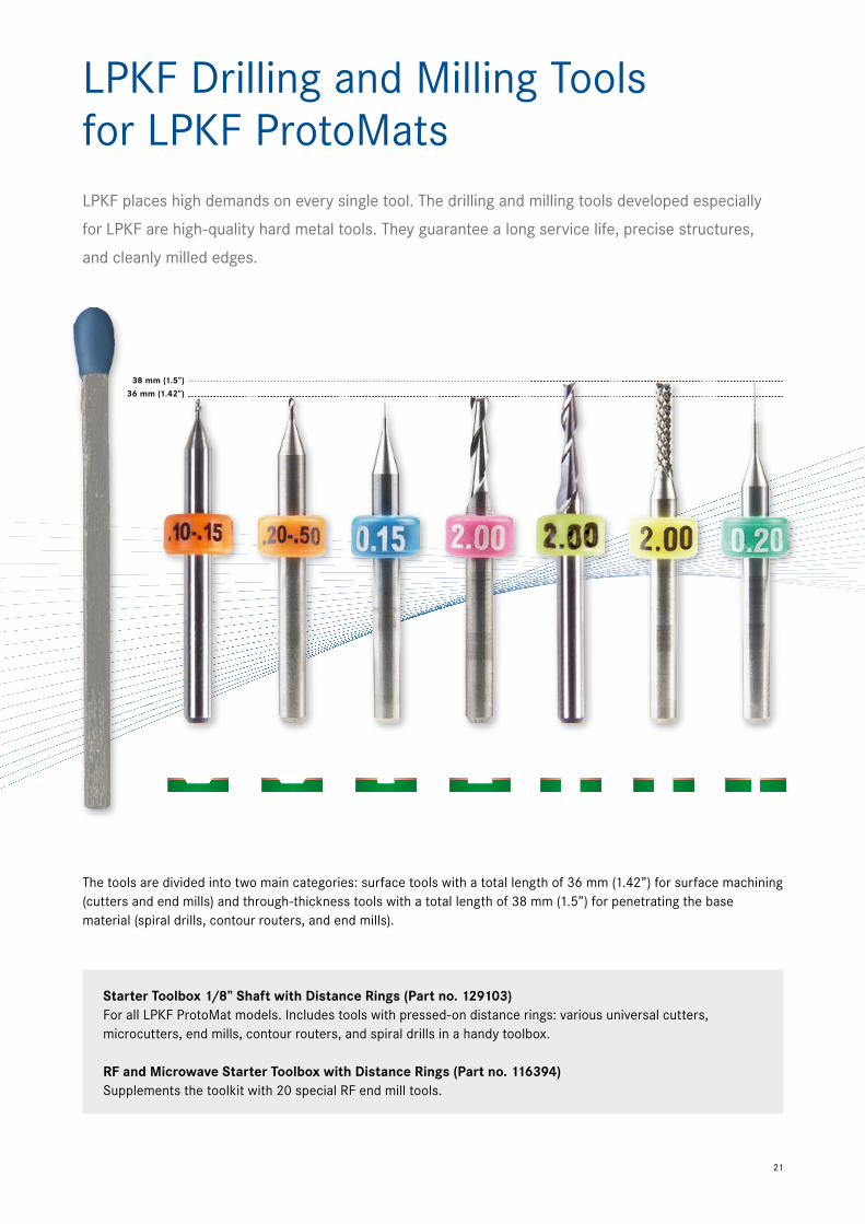
LPKF Drilling and Milling Tools for LPKF ProtoMatsLPKF places high demands on every single tool. The drilling and milling tools developed especially
for LPKF are high-quality hard metal tools. They guarantee a long service life, precise structures,
and cleanly milled edges.
The tools are divided into two main categories: surface tools with a total length of 36 mm (1.42”) for surface machining (cutters and end mills) and through-thickness tools with a total length of 38 mm (1.5”) for penetrating the base material (spiral drills, contour routers, and end mills).
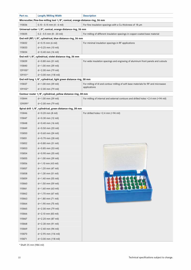
Starter Toolbox 1/8” Shaft with Distance Rings (Part no. 129103)For all LPKF ProtoMat models. Includes tools with pressed-on distance rings: various universal cutters, microcutters, end mills, contour routers, and spiral drills in a handy toolbox.
RF and Microwave Starter Toolbox with Distance Rings (Part no. 116394)Supplements the toolkit with 20 special RF end mill tools.
22
Part no. Length/Milling Width Description
Microcutter/fine-line milling tool 1/8”, conical, orange distance ring, 36 mm
115836 0.10 – 0.15 mm (4 – 6 mil) For fine insulation spacings with a Cu thickness of 18 µm
Universal cutter 1/8”, conical, orange distance ring, 36 mm
115835 0.2 – 0.5 mm (8 – 20 mil) For milling of different insulation spacings in copper-coated base material
End mill (RF) 1/8’’, cylindrical, blue distance ring, 36 mm
115832 d = 0.15 mm (6 mil) For minimal insulation spacings in RF applications
115833 d = 0.25 mm (10 mil)
115834 d = 0.40 mm (16 mil)
End mill 1/8’’, cylindrical, violet distance ring, 36 mm
115839 d = 0.80 mm (31 mil) For wide insulation spacings and engraving of aluminum front panels and cutouts
115840 d = 1.00 mm (39 mil)
129100* d = 2.00 mm (79 mil)
129101* d = 3.00 mm (118 mil)
End mill long 1/8’’, cylindrical, light green distance ring, 38 mm
115837 d = 1.00 mm (39 mil) For milling of Al and contour milling of soft base materials for RF and microwave applications
129102* d = 2.00 mm (79 mil)
Contour router 1/8”, cylindrical, yellow distance ring, 38 mm
115844 d = 1.00 mm (39 mil) For milling of internal and external contours and drilled holes > 2.4 mm (> 94 mil)
129099* d = 2.00 mm (79 mil)
Spiral drill 1/8”, cylindrical, green distance ring, 38 mm
115846 d = 0.20 mm (8 mil) For drilled holes < 2.4 mm (< 94 mil)
115847 d = 0.30 mm (12 mil)
115848 d = 0.40 mm (16 mil)
115849 d = 0.50 mm (20 mil)
115850 d = 0.60 mm (24 mil)
115851 d = 0.70 mm (28 mil)
115852 d = 0.80 mm (31 mil)
115853 d = 0.85 mm (33 mil)
115854 d = 0.90 mm (35 mil)
115855 d = 1.00 mm (39 mil)
115856 d = 1.10 mm (43 mil)
115857 d = 1.20 mm (47 mil)
115858 d = 1.30 mm (51 mil)
115859 d = 1.40 mm (55 mil)
115860 d = 1.50 mm (59 mil)
115861 d = 1.60 mm (63 mil)
115862 d = 1.70 mm (67 mil)
115863 d = 1.80 mm (71 mil)
115864 d = 1.90 mm (75 mil)
115865 d = 2.00 mm (79 mil)
115866 d = 2.10 mm (83 mil)
115867 d = 2.20 mm (87 mil)
115868 d = 2.30 mm (91 mil)
115869 d = 2.40 mm (94 mil)
115870 d = 2.95 mm (116 mil)
115871 d = 3.00 mm (118 mil)
* Shaft 25 mm (984 mil)
Technical specifications subject to change.
23
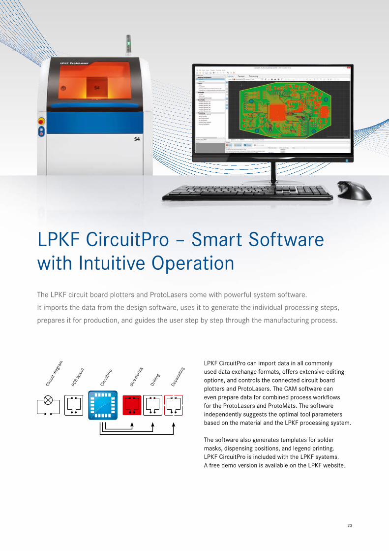
LPKF CircuitPro – Smart Software with Intuitive OperationThe LPKF circuit board plotters and ProtoLasers come with powerful system software.
It imports the data from the design software, uses it to generate the individual processing steps,
prepares it for production, and guides the user step by step through the manufacturing process.
LPKF CircuitPro can import data in all commonly used data exchange formats, offers extensive editing options, and controls the connected circuit board plotters and ProtoLasers. The CAM software can even prepare data for combined process workflows for the ProtoLasers and ProtoMats. The software independently suggests the optimal tool parameters based on the material and the LPKF processing system.
The software also generates templates for solder masks, dispensing positions, and legend printing. LPKF CircuitPro is included with the LPKF systems. A free demo version is available on the LPKF website.
Circ
uit d
iagr
am
PCB
layo
ut
Circ
uitP
ro
Stru
ctur
ing
Drill
ing
Depa
nelin
g
24
LPKF CircuitPro
Import formats for PCB processing
Gerber Standard (RS-274-D), Extended Gerber (RS-274-X), Excellon NC Drill (Versions 1 and 2),Sieb & Meier NC Drill, HP-GL™, DPF, Auto-CAD™ DXF, IGES, LMD, STEP
PCB Prototyping with Software SupportPowerful and user-friendly: these two attributes were at the top of the list of requirements during development of the LPKF CircuitPro system software. Even less experienced users can produce complex PCB prototypes thanks to the well-thought-out user navigation.
LPKF CircuitPro is the result of 40 years of experience in the manufacturing of PCB prototypes. The software recognizes the necessary work steps and guides the user comfortably through the production process by means of wizards. Empirically proven process parameters for the main PCB materials are already available in libraries. LPKF CircuitPro precisely processes precisely the data required by PCB manufacturers.
CircuitPro automatically imports aperture tables and tool lists as well as Gerber and NC data, combines multiple PCBs on a panel, and employs methods for checking the layout. Refined software routines determine the most effective process sequence for the respective processing system and optimally use the available tools.
The user can load finished projects or easily optimize newly created production steps in the integrated editor.
• Powerful CAM software supplied with every ProtoMat and ProtoLaser – for optimized manufacturing processes
• Interactive process editor
• Intuitive operation – minimal training requirements
• Extensive data interfaces
• Reliable process control and monitoring
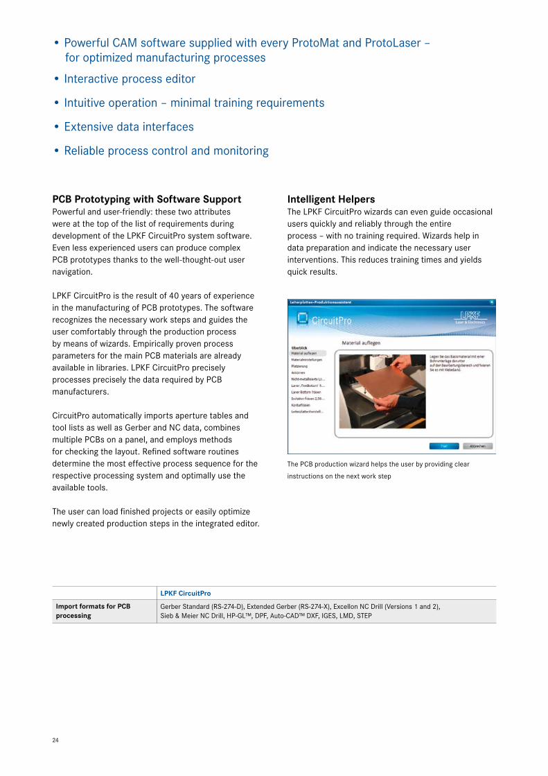
Intelligent HelpersThe LPKF CircuitPro wizards can even guide occasional users quickly and reliably through the entire process – with no training required. Wizards help in data preparation and indicate the necessary user interventions. This reduces training times and yields quick results.
The PCB production wizard helps the user by providing clear
instructions on the next work step
25
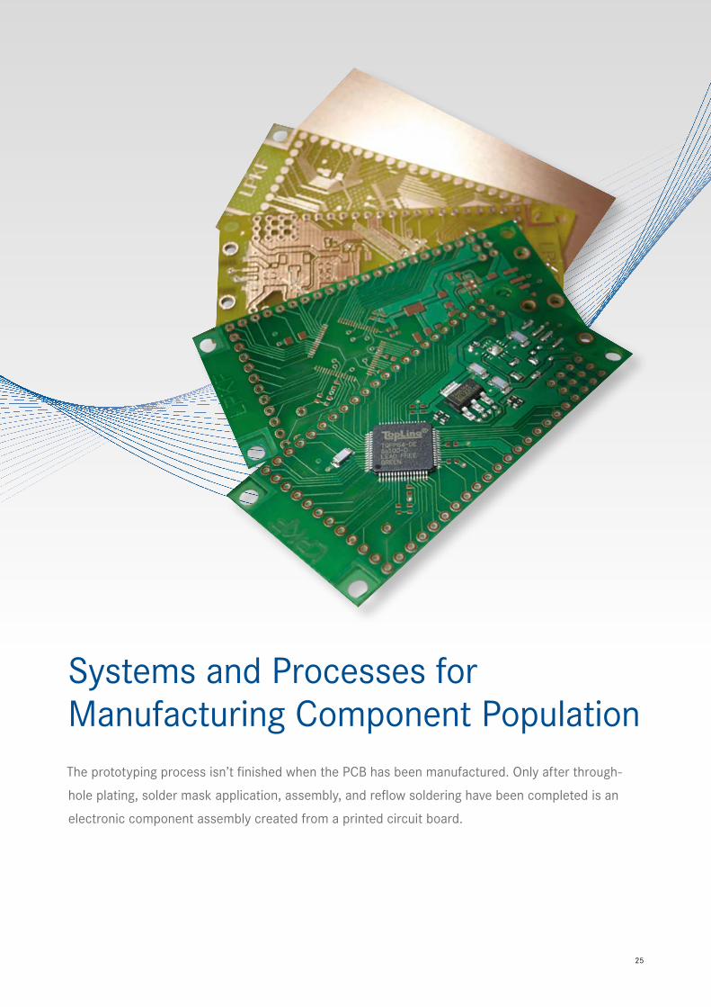
Systems and Processes for Manufacturing Component PopulationThe prototyping process isn’t finished when the PCB has been manufactured. Only after through-
hole plating, solder mask application, assembly, and reflow soldering have been completed is an
electronic component assembly created from a printed circuit board.
26
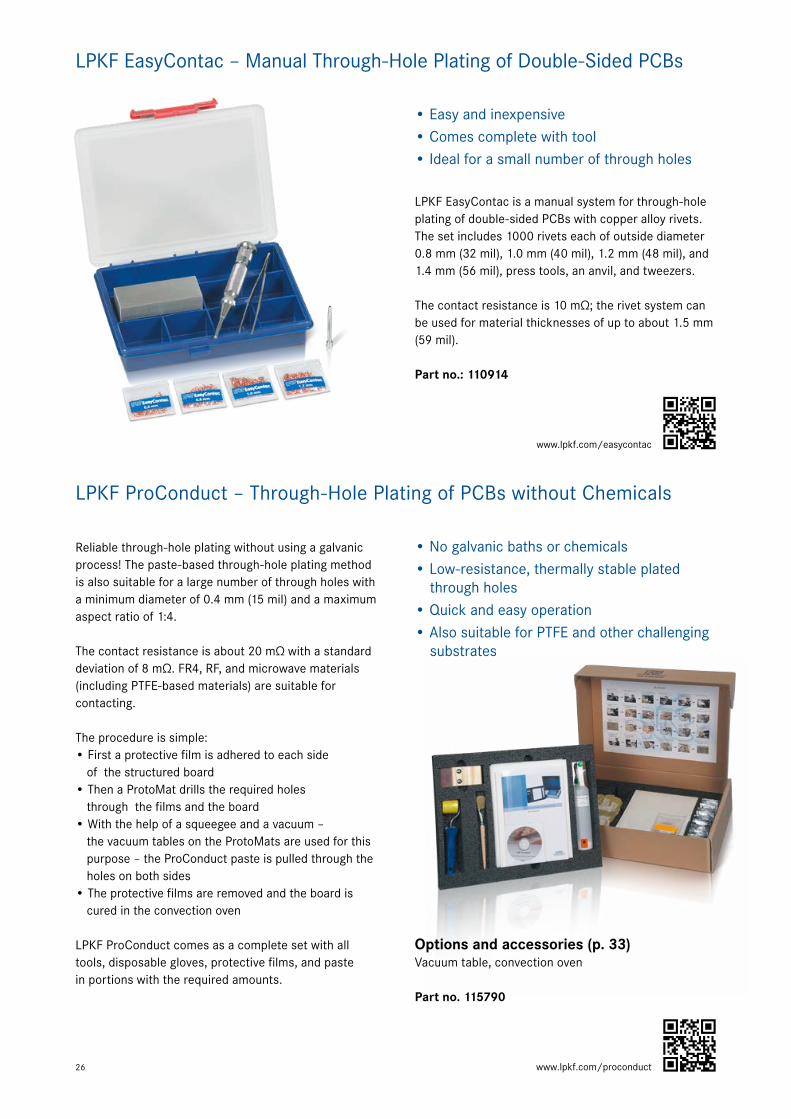
LPKF EasyContac is a manual system for through-hole plating of double-sided PCBs with copper alloy rivets. The set includes 1000 rivets each of outside diameter 0.8 mm (32 mil), 1.0 mm (40 mil), 1.2 mm (48 mil), and 1.4 mm (56 mil), press tools, an anvil, and tweezers.
The contact resistance is 10 mΩ; the rivet system can be used for material thicknesses of up to about 1.5 mm (59 mil).
Part no.: 110914
Reliable through-hole plating without using a galvanic process! The paste-based through-hole plating method is also suitable for a large number of through holes with a minimum diameter of 0.4 mm (15 mil) and a maximum aspect ratio of 1:4.
The contact resistance is about 20 mΩ with a standard deviation of 8 mΩ. FR4, RF, and microwave materials (including PTFE-based materials) are suitable for contacting.
The procedure is simple:• First a protective film is adhered to each side
of the structured board• Then a ProtoMat drills the required holes
through the films and the board• With the help of a squeegee and a vacuum –
the vacuum tables on the ProtoMats are used for this purpose – the ProConduct paste is pulled through the holes on both sides
• The protective films are removed and the board is cured in the convection oven
LPKF ProConduct comes as a complete set with all tools, disposable gloves, protective films, and paste in portions with the required amounts.
• Easy and inexpensive• Comes complete with tool• Ideal for a small number of through holes
• No galvanic baths or chemicals• Low-resistance, thermally stable plated
through holes• Quick and easy operation• Also suitable for PTFE and other challenging
substrates
Options and accessories (p. 33)Vacuum table, convection oven
LPKF EasyContac – Manual Through-Hole Plating of Double-Sided PCBs
LPKF ProConduct – Through-Hole Plating of PCBs without Chemicals
Part no. 115790
www.lpkf.com/easycontac
www.lpkf.com/proconduct
27
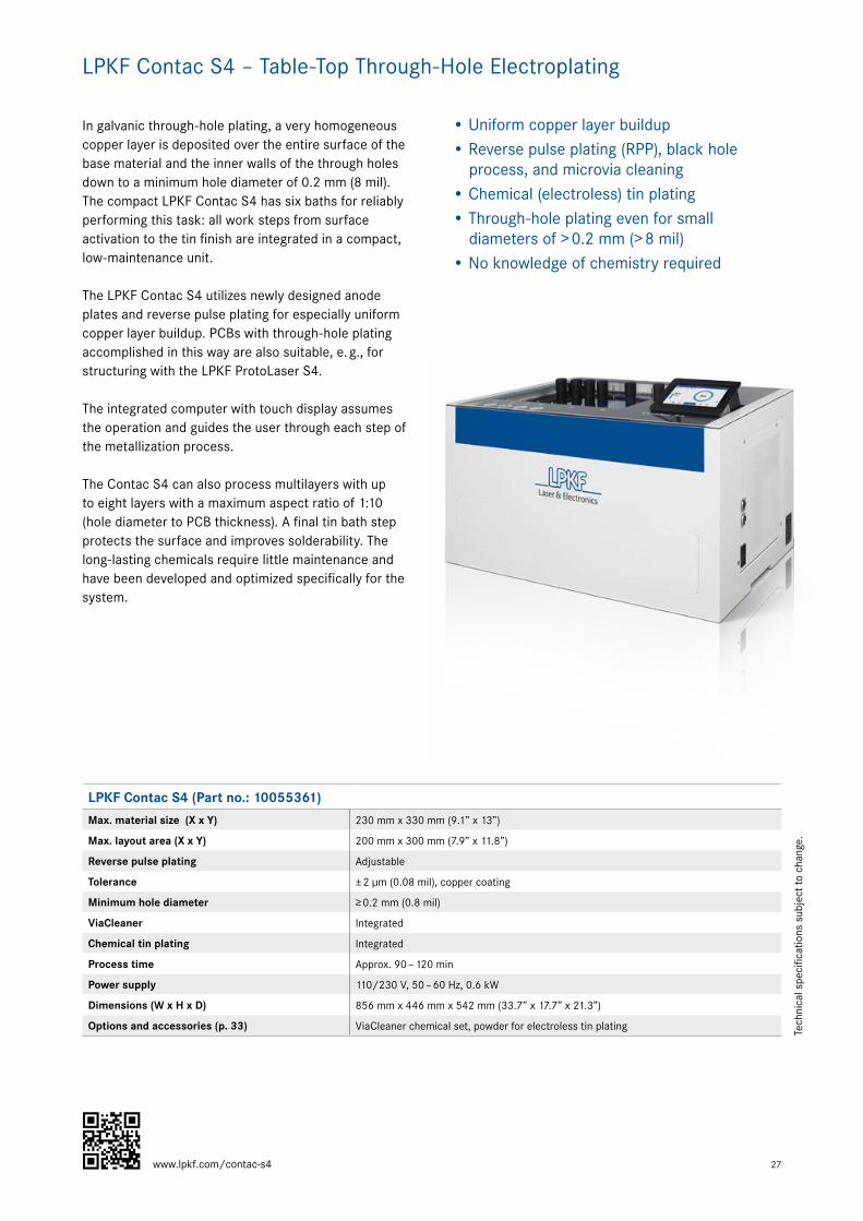
In galvanic through-hole plating, a very homogeneous copper layer is deposited over the entire surface of the base material and the inner walls of the through holes down to a minimum hole diameter of 0.2 mm (8 mil). The compact LPKF Contac S4 has six baths for reliably performing this task: all work steps from surface activation to the tin finish are integrated in a compact, low-maintenance unit.
The LPKF Contac S4 utilizes newly designed anode plates and reverse pulse plating for especially uniform copper layer buildup. PCBs with through-hole plating accomplished in this way are also suitable, e. g., for structuring with the LPKF ProtoLaser S4.
The integrated computer with touch display assumes the operation and guides the user through each step of the metallization process.
The Contac S4 can also process multilayers with up to eight layers with a maximum aspect ratio of 1:10 (hole diameter to PCB thickness). A final tin bath step protects the surface and improves solderability. The long-lasting chemicals require little maintenance and have been developed and optimized specifically for the system.
• Uniform copper layer buildup• Reverse pulse plating (RPP), black hole
process, and microvia cleaning• Chemical (electroless) tin plating• Through-hole plating even for small
diameters of > 0.2 mm (> 8 mil)• No knowledge of chemistry required
LPKF Contac S4 (Part no.: 10055361)
Max. material size (X x Y) 230 mm x 330 mm (9.1” x 13”)
Max. layout area (X x Y) 200 mm x 300 mm (7.9” x 11.8”)
Reverse pulse plating Adjustable
Tolerance ± 2 µm (0.08 mil), copper coating
Minimum hole diameter ≥ 0.2 mm (0.8 mil)
ViaCleaner Integrated
Chemical tin plating Integrated
Process time Approx. 90 – 120 min
Power supply 110/230 V, 50 – 60 Hz, 0.6 kW
Dimensions (W x H x D) 856 mm x 446 mm x 542 mm (33.7” x 17.7” x 21.3”)
Options and accessories (p. 33) ViaCleaner chemical set, powder for electroless tin plating
LPKF Contac S4 – Table-Top Through-Hole Electroplating
Tech
nica
l spe
cific
atio
ns s
ubje
ct to
cha
nge.
www.lpkf.com/contac-s4
28
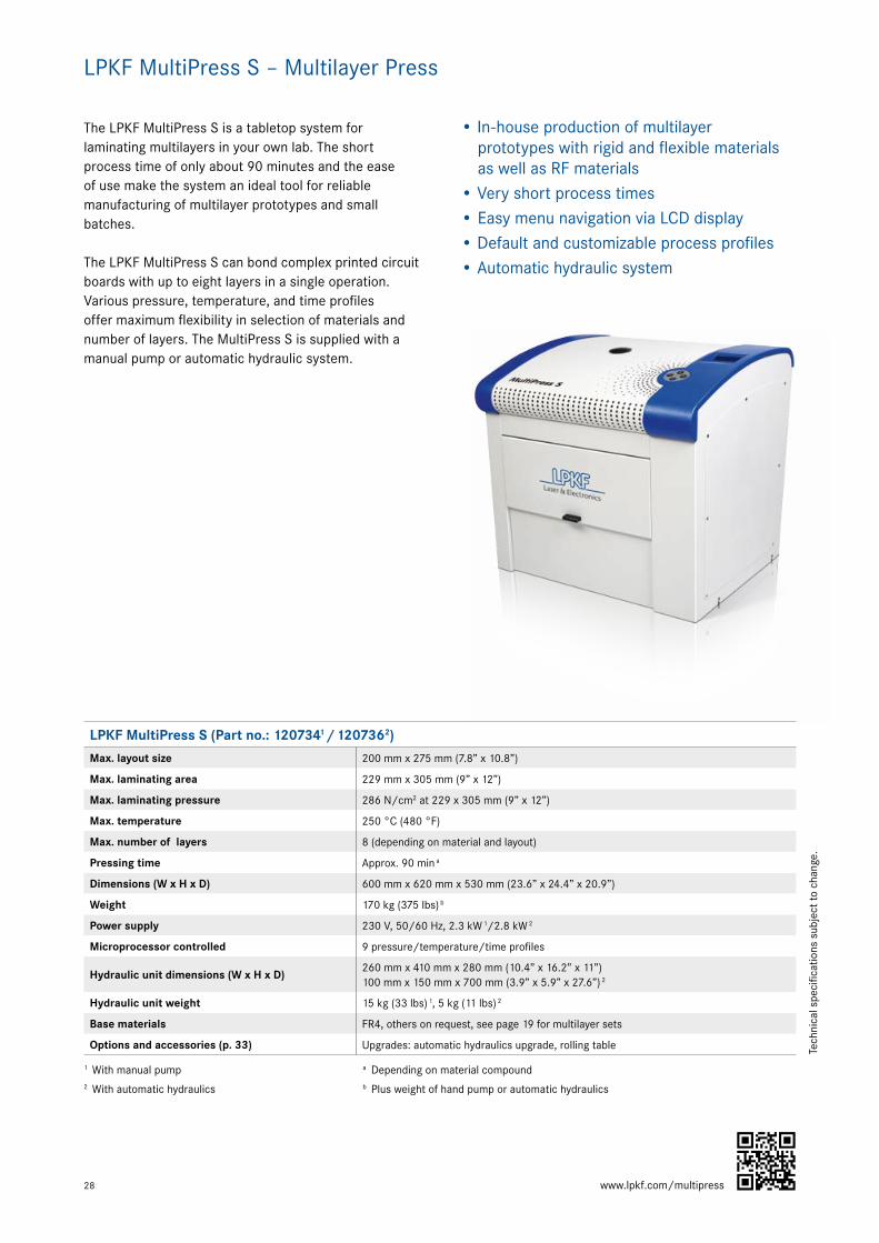
The LPKF MultiPress S is a tabletop system for laminating multilayers in your own lab. The short process time of only about 90 minutes and the ease of use make the system an ideal tool for reliable manufacturing of multilayer prototypes and small batches.
The LPKF MultiPress S can bond complex printed circuit boards with up to eight layers in a single operation. Various pressure, temperature, and time profiles offer maximum flexibility in selection of materials and number of layers. The MultiPress S is supplied with a manual pump or automatic hydraulic system.
• In-house production of multilayer prototypes with rigid and flexible materials as well as RF materials
• Very short process times • Easy menu navigation via LCD display• Default and customizable process profiles• Automatic hydraulic system
LPKF MultiPress S – Multilayer Press
LPKF MultiPress S (Part no.: 1207341 / 1207362)
Max. layout size 200 mm x 275 mm (7.8” x 10.8”)
Max. laminating area 229 mm x 305 mm (9” x 12”)
Max. laminating pressure 286 N/cm2 at 229 x 305 mm (9” x 12”)
Max. temperature 250 °C (480 °F)
Max. number of layers 8 (depending on material and layout)
Pressing time Approx. 90 min a
Dimensions (W x H x D) 600 mm x 620 mm x 530 mm (23.6” x 24.4” x 20.9”)
Weight 170 kg (375 lbs) b
Power supply 230 V, 50/60 Hz, 2.3 kW 1/2.8 kW 2
Microprocessor controlled 9 pressure/temperature/time profiles
Hydraulic unit dimensions (W x H x D)260 mm x 410 mm x 280 mm (10.4” x 16.2” x 11”)100 mm x 150 mm x 700 mm (3.9” x 5.9” x 27.6”) 2
Hydraulic unit weight 15 kg (33 lbs) 1, 5 kg (11 lbs) 2
Base materials FR4, others on request, see page 19 for multilayer sets
Options and accessories (p. 33) Upgrades: automatic hydraulics upgrade, rolling table
1 With manual pump2 With automatic hydraulics
a Depending on material compoundb Plus weight of hand pump or automatic hydraulics
Tech
nica
l spe
cific
atio
ns s
ubje
ct to
cha
nge.
www.lpkf.com/multipress
29
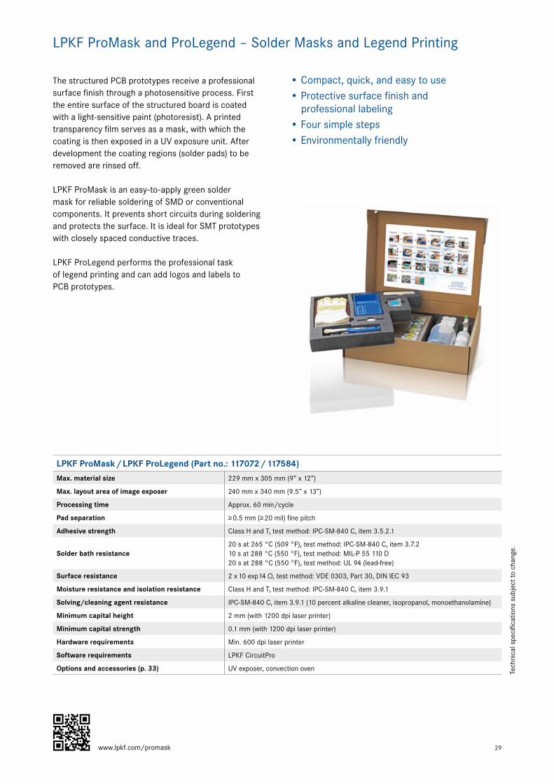
The structured PCB prototypes receive a professional surface finish through a photosensitive process. First the entire surface of the structured board is coated with a light-sensitive paint (photoresist). A printed transparency film serves as a mask, with which the coating is then exposed in a UV exposure unit. After development the coating regions (solder pads) to be removed are rinsed off.
LPKF ProMask is an easy-to-apply green solder mask for reliable soldering of SMD or conventional components. It prevents short circuits during soldering and protects the surface. It is ideal for SMT prototypes with closely spaced conductive traces.
LPKF ProLegend performs the professional task of legend printing and can add logos and labels to PCB prototypes.
• Compact, quick, and easy to use• Protective surface finish and
professional labeling• Four simple steps• Environmentally friendly
LPKF ProMask and ProLegend – Solder Masks and Legend Printing
Tech
nica
l spe
cific
atio
ns s
ubje
ct to
cha
nge.
LPKF ProMask / LPKF ProLegend (Part no.: 117072 / 117584)
Max. material size 229 mm x 305 mm (9” x 12”)
Max. layout area of image exposer 240 mm x 340 mm (9.5” x 13”)
Processing time Approx. 60 min/cycle
Pad separation ≥ 0.5 mm (≥ 20 mil) fine pitch
Adhesive strength Class H and T, test method: IPC-SM-840 C, item 3.5.2.1
Solder bath resistance20 s at 265 °C (509 °F), test method: IPC-SM-840 C, item 3.7.2 10 s at 288 °C (550 °F), test method: MIL-P 55 110 D20 s at 288 °C (550 °F), test method: UL 94 (lead-free)
Surface resistance 2 x 10 exp14 Ω, test method: VDE 0303, Part 30, DIN IEC 93
Moisture resistance and isolation resistance Class H and T, test method: IPC-SM-840 C, item 3.9.1
Solving/cleaning agent resistance IPC-SM-840 C, item 3.9.1 (10 percent alkaline cleaner, isopropanol, monoethanolamine)
Minimum capital height 2 mm (with 1200 dpi laser printer)
Minimum capital strength 0.1 mm (with 1200 dpi laser printer)
Hardware requirements Min. 600 dpi laser printer
Software requirements LPKF CircuitPro
Options and accessories (p. 33) UV exposer, convection oven
www.lpkf.com/promask
30
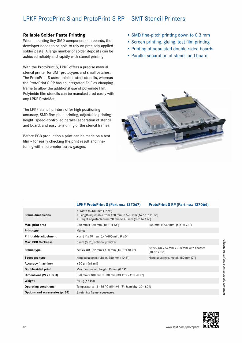
Reliable Solder Paste PrintingWhen mounting tiny SMD components on boards, the developer needs to be able to rely on precisely applied solder paste. A large number of solder deposits can be achieved reliably and rapidly with stencil printing.
With the ProtoPrint S, LPKF offers a precise manual stencil printer for SMT prototypes and small batches. The ProtoPrint S uses stainless steel stencils, whereas the ProtoPrint S RP has an integrated ZelFlex clamping frame to allow the additional use of polyimide film. Polyimide film stencils can be manufactured easily with any LPKF ProtoMat.
The LPKF stencil printers offer high positioning accuracy, SMD fine-pitch printing, adjustable printing height, speed-controlled parallel separation of stencil and board, and easy tensioning of the stencil frames.
Before PCB production a print can be made on a test film – for easily checking the print result and fine-tuning with micrometer screw gauges.
• SMD fine-pitch printing down to 0.3 mm• Screen printing, gluing, test film printing• Printing of populated double-sided boards• Parallel separation of stencil and board
LPKF ProtoPrint S and ProtoPrint S RP – SMT Stencil Printers
Tech
nica
l spe
cific
atio
ns s
ubje
ct to
cha
nge.
LPKF ProtoPrint S (Part no.: 127067) ProtoPrint S RP (Part no.: 127066)
Frame dimensions• Width to 430 mm (16.9”)• Length adjustable from 420 mm to 520 mm (16.5” to 20.5”)• Height adjustable from 20 mm to 40 mm (0.8” to 1.6”)
Max. print area 260 mm x 330 mm (10.2” x 13”) 164 mm x 230 mm (6.5” x 9.1”)
Print type Manual
Print table adjustment X and Y ± 10 mm (0.4”/400 mil), ϑ ± 5°
Max. PCB thickness 5 mm (0.2”), optionally thicker
Frame type Zelflex QR 362 mm x 480 mm (14.3” x 18.9”)Zelflex QR 266 mm x 380 mm with adapter (10.5” x 15”)
Squeegee type Hand squeegee, rubber, 260 mm (10.2”) Hand squeegee, metal, 180 mm (7”)
Accuracy (machine) ± 20 µm (±1 mil)
Double-sided print Max. component height 15 mm (0.59”)
Dimensions (W x H x D) 850 mm x 180 mm x 530 mm (33.4” x 7.1” x 20.9”)
Weight 30 kg (66 lbs)
Operating conditions Temperature: 15 – 35 °C (59 – 95 °F); humidity: 30 – 80 %
Options and accessories (p. 34) Stretching frame, squeegees
www.lpkf.com/protoprint
31
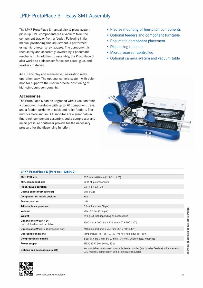
The LPKF ProtoPlace S manual pick & place system picks up SMD components via a vacuum from the component tray or from a feeder. Following initial manual positioning fine adjustment is performed using micrometer screw gauges. The component is then safely and accurately lowered by a pneumatic mechanism. In addition to assembly, the ProtoPlace S also works as a dispenser for solder paste, glue, and auxiliary materials.
An LCD display and menu-based navigation make operation easy. The optional camera system with color monitor supports the user in precise positioning of high-pin-count components.
AccessoriesThe ProtoPlace S can be upgraded with a vacuum table, a component turntable with up to 90 component trays, and a feeder carrier with stick and roller feeders. The microcamera and an LCD monitor are a great help in fine-pitch component assembly, and a compressor and an air pressure controller provide for the necessary pressure for the dispensing function.
• Precise mounting of fine-pitch components• Optional feeders and component turntable• Pneumatic component placement• Dispensing function• Microprocessor controlled• Optional camera system and vacuum table
LPKF ProtoPlace S – Easy SMT Assembly
Tech
nica
l spe
cific
atio
ns s
ubje
ct to
cha
nge.
LPKF ProtoPlace S (Part no.: 126979)
Max. PCB size 297 mm x 420 mm (11.8” x 16.5”)
Min. component size 0201 chip components
Pulse/pause duration 0.1 – 9 s / 0.1 – 2 s
Dosing quantity (Dispenser) Min. 0.2 µl
Component turntable position Rear
Feeder position Left
Adjustable air pressure 0.1 – 4 bar (1.4 – 58 psi)
Vacuum Max. 0.8 bar (11.6 psi)
Weight 29 kg (64 lbs) depending on accessories
Dimensions (W x H x D) (with all feeders and turntable)
1000 mm x 500 mm x 900 mm (40” x 20” x 35”)
Dimensions (W x H x D) (machine only) 760 mm x 250 mm x 760 mm (30” x 10” x 30”)
Operating conditions Temperature: 15 – 35 °C, (59 – 95 °F); humidity: 30 – 80 %
Compressed air supply 8 bar (116 psi), min. 50 L/min (1.76 cfm), unlubricated, waterless
Power supply 115/230 V, 50 – 60 Hz, 10 W
Options and accessories (p. 34) Vacuum table, component turntable, feeder carrier (stick/roller feeders), microcamera, LCD monitor, compressor, and air pressure regulator
www.lpkf.com/protoplace
32
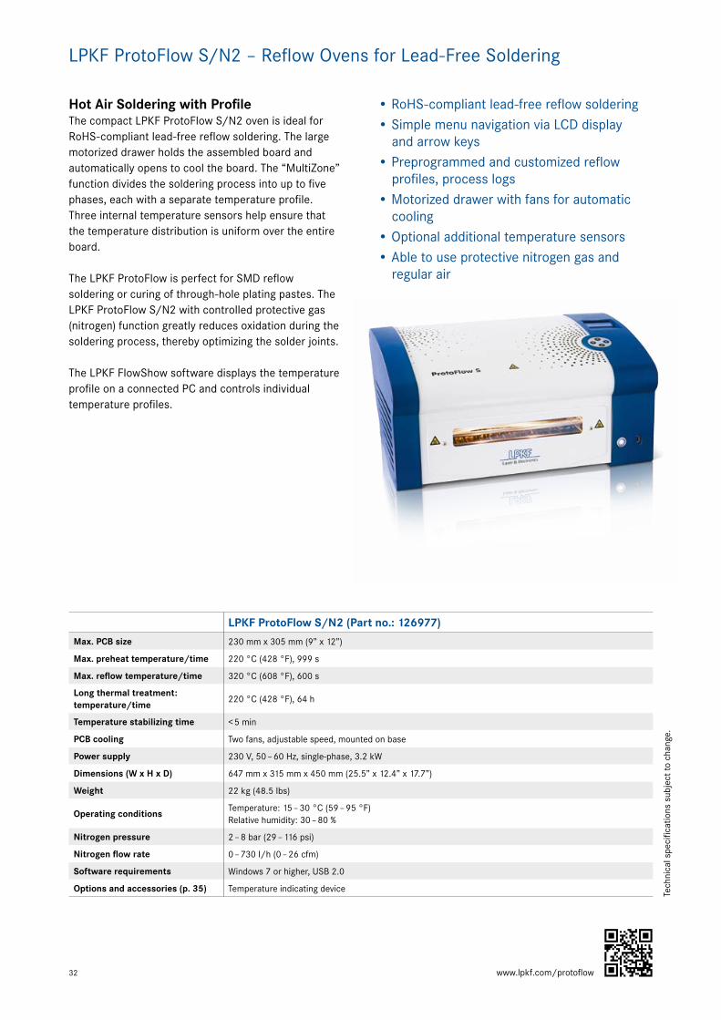
Hot Air Soldering with ProfileThe compact LPKF ProtoFlow S/N2 oven is ideal for RoHS-compliant lead-free reflow soldering. The large motorized drawer holds the assembled board and automatically opens to cool the board. The “MultiZone” function divides the soldering process into up to five phases, each with a separate temperature profile. Three internal temperature sensors help ensure that the temperature distribution is uniform over the entire board.
The LPKF ProtoFlow is perfect for SMD reflow soldering or curing of through-hole plating pastes. The LPKF Proto Flow S/N2 with controlled protective gas (nitrogen) function greatly reduces oxidation during the soldering process, thereby optimizing the solder joints.
The LPKF FlowShow software displays the temperature profile on a connected PC and controls individual temperature profiles.
• RoHS-compliant lead-free reflow soldering• Simple menu navigation via LCD display
and arrow keys• Preprogrammed and customized reflow
profiles, process logs• Motorized drawer with fans for automatic
cooling• Optional additional temperature sensors• Able to use protective nitrogen gas and
regular air
LPKF ProtoFlow S/N2 – Reflow Ovens for Lead-Free Soldering
Tech
nica
l spe
cific
atio
ns s
ubje
ct to
cha
nge.
LPKF ProtoFlow S/N2 (Part no.: 126977)
Max. PCB size 230 mm x 305 mm (9” x 12”)
Max. preheat temperature/time 220 °C (428 °F), 999 s
Max. reflow temperature/time 320 °C (608 °F), 600 s
Long thermal treatment: temperature/time
220 °C (428 °F), 64 h
Temperature stabilizing time < 5 min
PCB cooling Two fans, adjustable speed, mounted on base
Power supply 230 V, 50 – 60 Hz, single-phase, 3.2 kW
Dimensions (W x H x D) 647 mm x 315 mm x 450 mm (25.5” x 12.4” x 17.7”)
Weight 22 kg (48.5 lbs)
Operating conditionsTemperature: 15 – 30 °C (59 – 95 °F)Relative humidity: 30 – 80 %
Nitrogen pressure 2 – 8 bar (29 – 116 psi)
Nitrogen flow rate 0 – 730 l/h (0 – 26 cfm)
Software requirements Windows 7 or higher, USB 2.0
Options and accessories (p. 35) Temperature indicating device
www.lpkf.com/protoflow
33
Accessories for SMT Systems and Processes
Accessories for Through-Hole Plating with LPKF ProConduct
Accessories for LPKF ProMask and LPKF ProLegend
Accessories for LPKF Contac S4
Accessories for Pressing of Multilayers with the LPKF MultiPress S
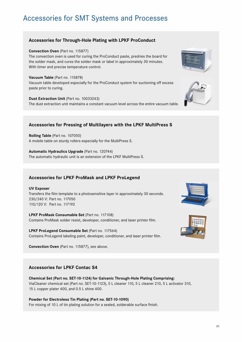
Convection Oven (Part no. 115877)The convection oven is used for curing the ProConduct paste, predries the board for the solder mask, and cures the solder mask or label in approximately 30 minutes. With timer and precise temperature control.
Convection Oven (Part no. 115877), see above.
Chemical Set (Part no. SET-10-1124) for Galvanic Through-Hole Plating Comprising:ViaCleaner chemical set (Part no. SET-10-1123), 5 L cleaner 110, 5 L cleaner 210, 5 L activator 310,15 L copper plater 400, and 0.5 L shine 400.
Powder for Electroless Tin Plating (Part no. SET-10-1090) For mixing of 10 L of tin plating solution for a sealed, solderable surface finish.
Rolling Table (Part no. 107050)A mobile table on sturdy rollers especially for the MultiPress S.
Automatic Hydraulics Upgrade (Part no. 120744)The automatic hydraulic unit is an extension of the LPKF MultiPress S.
Vacuum Table (Part no. 115878)Vacuum table developed especially for the ProConduct system for suctioning off excess paste prior to curing.
LPKF ProMask Consumable Set (Part no. 117108)Contains ProMask solder resist, developer, conditioner, and laser printer film.
LPKF ProLegend Consumable Set (Part no. 117564)Contains ProLegend labeling paint, developer, conditioner, and laser printer film.
UV Exposer Transfers the film template to a photosensitive layer in approximately 30 seconds. 230/240 V: Part no. 117050110/120 V: Part no. 117192
Dust Extraction Unit (Part no. 10033243)The dust extraction unit maintains a constant vacuum level across the entire vacuum table.
34
SqueegeeVarious squeegees for applying solder paste.Hand-held squeegee, rubber, 180 mm (7”): Part no. 10023549Hand-held squeegee, rubber, 260 mm (10.2”): Part no. 108140Hand-held squeegee, metal, 180 mm (7”): Part no. 10023958Hand-held squeegee, metal, 260 mm (10.2”): Part no. 124870Hand-held squeegee, Permalex, 180 mm (7”): Part no. 10023550Hand-held squeegee, Permalex, 260 mm (10.2”): Part no. 122257
Accessories for LPKF ProtoPrint S / ProtoPrint S RP
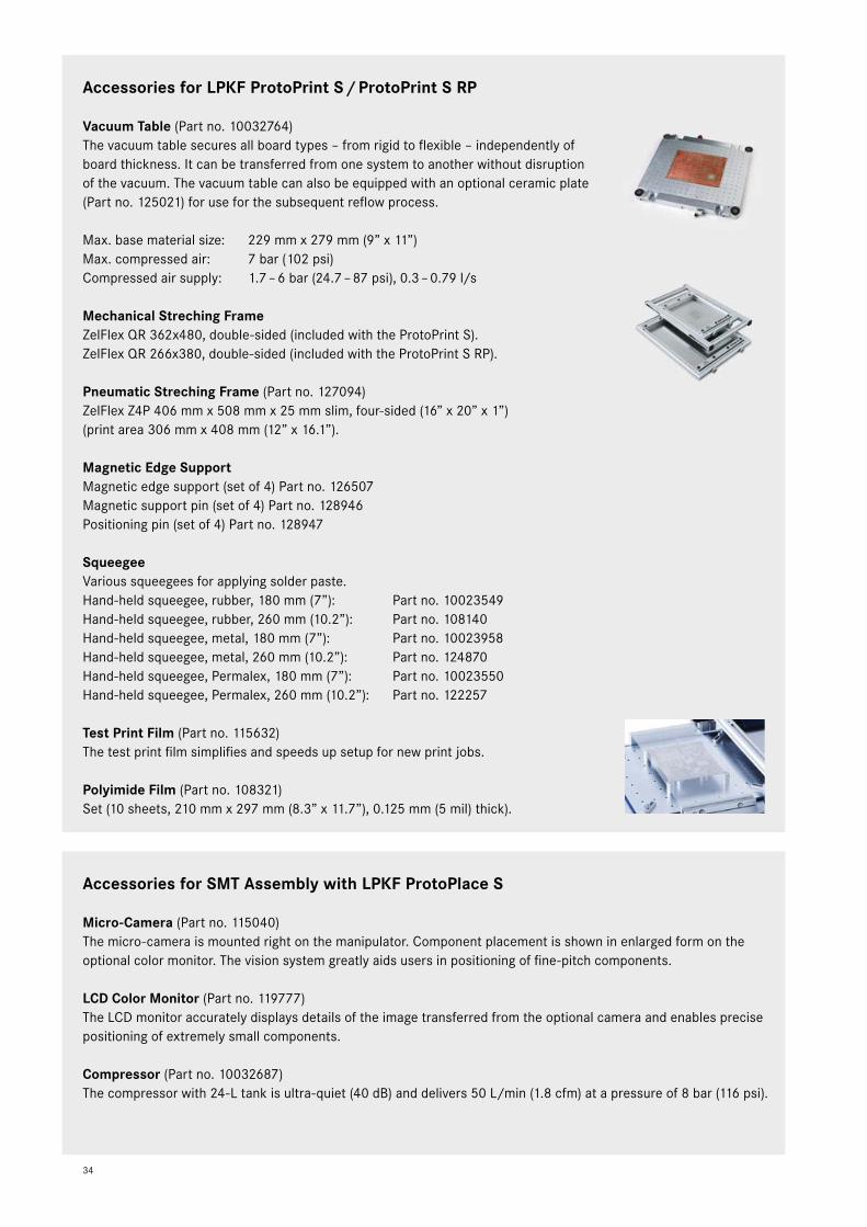
Vacuum Table (Part no. 10032764)The vacuum table secures all board types – from rigid to flexible – independently of board thickness. It can be transferred from one system to another without disruption of the vacuum. The vacuum table can also be equipped with an optional ceramic plate (Part no. 125021) for use for the subsequent reflow process.
Max. base material size: 229 mm x 279 mm (9” x 11”)Max. compressed air: 7 bar (102 psi)Compressed air supply: 1.7 – 6 bar (24.7 – 87 psi), 0.3 – 0.79 l/s
Magnetic Edge Support Magnetic edge support (set of 4) Part no. 126507Magnetic support pin (set of 4) Part no. 128946Positioning pin (set of 4) Part no. 128947
Mechanical Streching FrameZelFlex QR 362x480, double-sided (included with the ProtoPrint S). ZelFlex QR 266x380, double-sided (included with the ProtoPrint S RP).
Pneumatic Streching Frame (Part no. 127094)ZelFlex Z4P 406 mm x 508 mm x 25 mm slim, four-sided (16” x 20” x 1”)(print area 306 mm x 408 mm (12” x 16.1”).
Test Print Film (Part no. 115632)The test print film simplifies and speeds up setup for new print jobs.
Polyimide Film (Part no. 108321) Set (10 sheets, 210 mm x 297 mm (8.3” x 11.7”), 0.125 mm (5 mil) thick).
Accessories for SMT Assembly with LPKF ProtoPlace S
Micro-Camera (Part no. 115040)The micro-camera is mounted right on the manipulator. Component placement is shown in enlarged form on the optional color monitor. The vision system greatly aids users in positioning of fine-pitch components.
LCD Color Monitor (Part no. 119777)The LCD monitor accurately displays details of the image transferred from the optional camera and enables precise positioning of extremely small components.
Compressor (Part no. 10032687)The compressor with 24-L tank is ultra-quiet (40 dB) and delivers 50 L/min (1.8 cfm) at a pressure of 8 bar (116 psi).
35
Accessories for ProtoPlace E / ProtoPrint E
Magnetic Fixing PinsSet of magnetic fixing pins (Part no. 10015381). For double-sided printing: magnetic edge supports (4 pieces), magnetic support pins (4 pieces), magnetic positioning pins (2 pieces).
Magnetic edge supports with corner brackets (4 pieces), Part no. 126507Magnetic support pins (4 pieces), Part no. 10015383Magnetic positioning pins (2 pieces), Part no. 10015385
Motorized Components TurntableThe motorized components turntable considerably accelerates component pick-up. The components are stored in trays that can be labeled.45 component trays: Part no. 11446075 component trays: Part no. 11446190 component trays: Part no. 114462
Stick FeederThe LPKF ProtoPlace can accommodate stick feeders for various components. S08–S028: Part no. 101356S08L–S028L: Part no. 101356PLCC28–PLCC44: Part no. 101357PLCC52–PLCC84: Part no. 103897
Feeder Carrier (Part no. 115590)The feeder carrier can hold up to 12 feeders simultaneously. It is required for the additional roller or stick feeders.
Roller FeederRoller feeders for components with various widths are available for use with the LPKF ProtoPlace.Roller feeder 8 mm: Part no. 116004Roller feeder 12 mm: Part no. 116008Roller feeder 16 mm: Part no. 116009
Accessories for Reflow Soldering with the LPKF ProtoFlow S/N2
Vacuum Table (Part no. 119684), see page 34.
Air Pressure Regulator (Part no. 124919)Air pressure regulator with water separator and 5-µm particle filter for side installation on the ProtoPlace S.
Temperature Indicating Device (Part no. 117850)An add-on module with four freely positionable temperature sensors supplements the LPKF ProtoFlow S/N2. The temperature sensors transmit the exact temperatures of critical components or the board in real time. The temperature profiles of all four sensors are displayed in a temperature-time graph on a monitor and saved for later analysis. The profile writer requires a PC with USB interface as well as standard (spreadsheet) software.
36
Scientific Prototyping – Laser Systems for Development and ScienceLPKF offers a comprehensive program of coordinated machines and processes for PCB prototyping.
New laser systems for special tasks have continually been developed and are now combined under
the category “Scientific Prototyping.”
LPKF ProtoLaser U4The ProtoLaser U4 is a laser system with wide-ranging processing capabilities thanks to its UV laser source. The ProtoLaser U4 can structure and cut PCBs, process ceramics and LTCCs, structure thin films, or ablate invisible TCO layers on transparent substrates.
The ProtoLaser U4 features stability in the lower output range and power measurement on the substrate plane for challenging material processing tasks in R&D laboratories as well as for small batches.
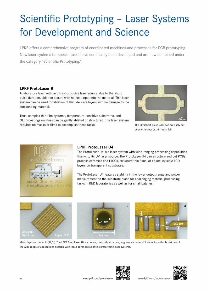
LPKF ProtoLaser RA laboratory laser with an ultrashort-pulse laser source: due to the short pulse duration, ablation occurs with no heat input into the material. This laser system can be used for ablation of thin, delicate layers with no damage to the surrounding material. Thus, complex thin-film systems, temperature-sensitive substrates, and OLED coatings on glass can be gently ablated or structured. The laser system requires no masks or films to accomplish these tasks.
100 µm
The ultrashort-pulse laser can precisely cut
geometries out of thin metal foil
Metal layers on ceramic (Al2O3): The LPKF ProtoLaser U4 can score, precisely structure, engrave, and even drill ceramics – this is just one of
the wide range of applications possible with these advanced scientific prototyping laser systems.
1 23
0.4 mm
0.6 mm
21
55 µm
58 µm 250 µm
3
Line/gap: 50/15 µm Angle: 135°
www.lpkf.com/protolaser-u4www.lpkf.com/protolaser-r
37
Conductive Traces on 3D Plastic Parts – LPKF ProtoLaser 3DThe LDS process generates traces on three-dimensional plastic parts
using a laser and a subsequent metallization process. A 3D MID
combines both mechanical and electronic functions in a single
device: a Mechatronic Integrated Devices (MID).
Laser Direct Structuring (LDS) is assuming a leading role for MIDs. A laser writes the conductive pattern on LDS-doped injection-molded parts. The traces are built up in a subsequent metallization bath.
In LDS prototyping, for example, plastic parts made by 3D printers are used. The base part is coated with LPKF ProtoPaint LDS, which contains the LDS additives.
The ProtoLaser 3D performs the laser structuring. The system features a height-adjustable working stage for structuring of parts of various dimensions.
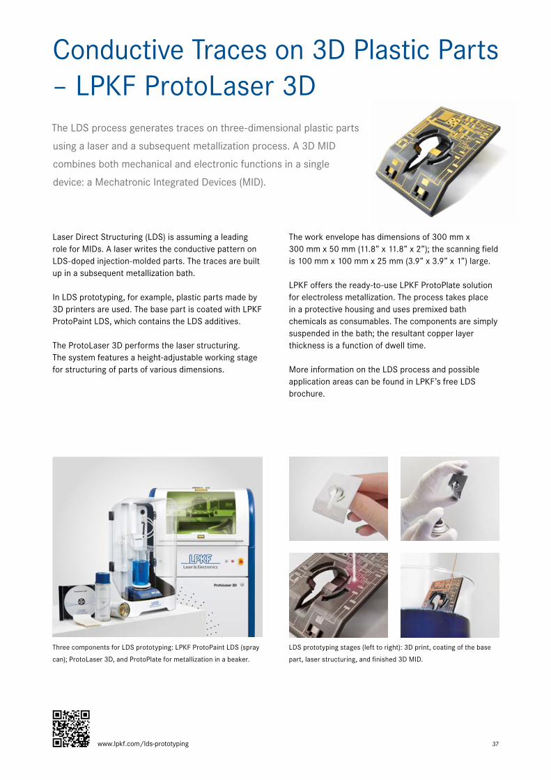
LDS prototyping stages (left to right): 3D print, coating of the base
part, laser structuring, and finished 3D MID.
Three components for LDS prototyping: LPKF ProtoPaint LDS (spray
can); ProtoLaser 3D, and ProtoPlate for metallization in a beaker.
The work envelope has dimensions of 300 mm x 300 mm x 50 mm (11.8” x 11.8” x 2”); the scanning field is 100 mm x 100 mm x 25 mm (3.9” x 3.9” x 1”) large.
LPKF offers the ready-to-use LPKF ProtoPlate solution for electroless metallization. The process takes place in a protective housing and uses premixed bath chemicals as consumables. The components are simply suspended in the bath; the resultant copper layer thickness is a function of dwell time.
More information on the LDS process and possible application areas can be found in LPKF’s free LDS brochure.
www.lpkf.com/lds-prototyping
38
LPKF has made a name for itself with systems for easy PCB prototyping. However, that’s not all
the Germany-based mechanical engineering specialist has to offer: the company sees itself as a
specialist in micro material processing, almost always using a laser.
Successful micro material processing requires several core competencies – which LPKF has developed over the course of many years. For example, specialized laser sources are developed and manufactured in-house: laser micro material processing poses different challenges than welding of thick sheet steel does.
Devices manufactured using LPKF systems and processes can be found in the electronics, medical technology, and automotive industries as well as in sophisticated consumer products.
Micro Material Processing Specialist
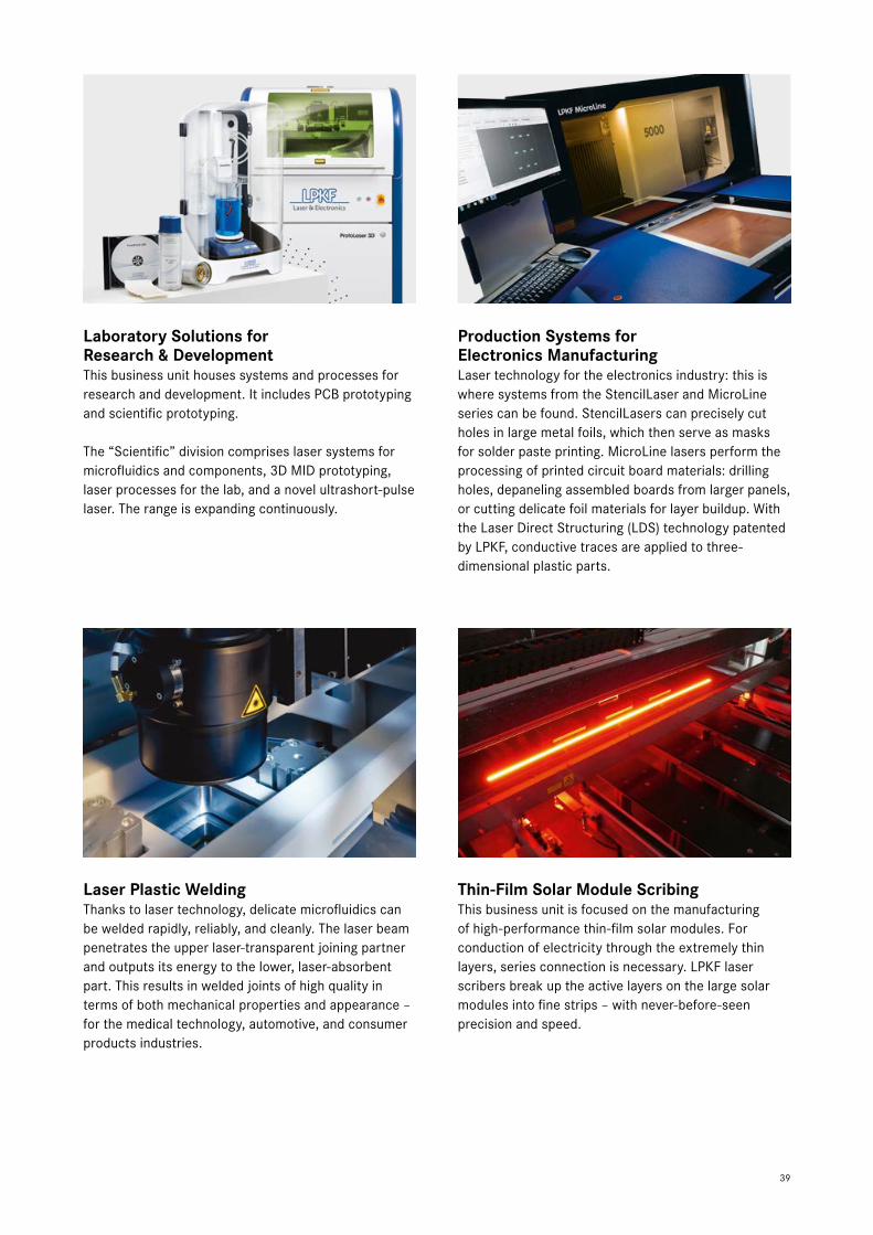
Micro material processing with
the laser
Laser technology &
optics
Precision drive
technology
Control technology &
software
Material technology
39
Thin-Film Solar Module ScribingThis business unit is focused on the manufacturing of high-performance thin-film solar modules. For conduction of electricity through the extremely thin layers, series connection is necessary. LPKF laser scribers break up the active layers on the large solar modules into fine strips – with never-before-seen precision and speed.
Laboratory Solutions for Research & DevelopmentThis business unit houses systems and processes for research and development. It includes PCB prototyping and scientific prototyping.
The “Scientific” division comprises laser systems for microfluidics and components, 3D MID prototyping, laser processes for the lab, and a novel ultrashort-pulse laser. The range is expanding continuously.
Production Systems for Electronics ManufacturingLaser technology for the electronics industry: this is where systems from the StencilLaser and MicroLine series can be found. StencilLasers can precisely cut holes in large metal foils, which then serve as masks for solder paste printing. MicroLine lasers perform the processing of printed circuit board materials: drilling holes, depaneling assembled boards from larger panels, or cutting delicate foil materials for layer buildup. With the Laser Direct Structuring (LDS) technology patented by LPKF, conductive traces are applied to three-dimensional plastic parts.
Laser Plastic WeldingThanks to laser technology, delicate microfluidics can be welded rapidly, reliably, and cleanly. The laser beam penetrates the upper laser-transparent joining partner and outputs its energy to the lower, laser-absorbent part. This results in welded joints of high quality in terms of both mechanical properties and appearance – for the medical technology, automotive, and consumer products industries.
40
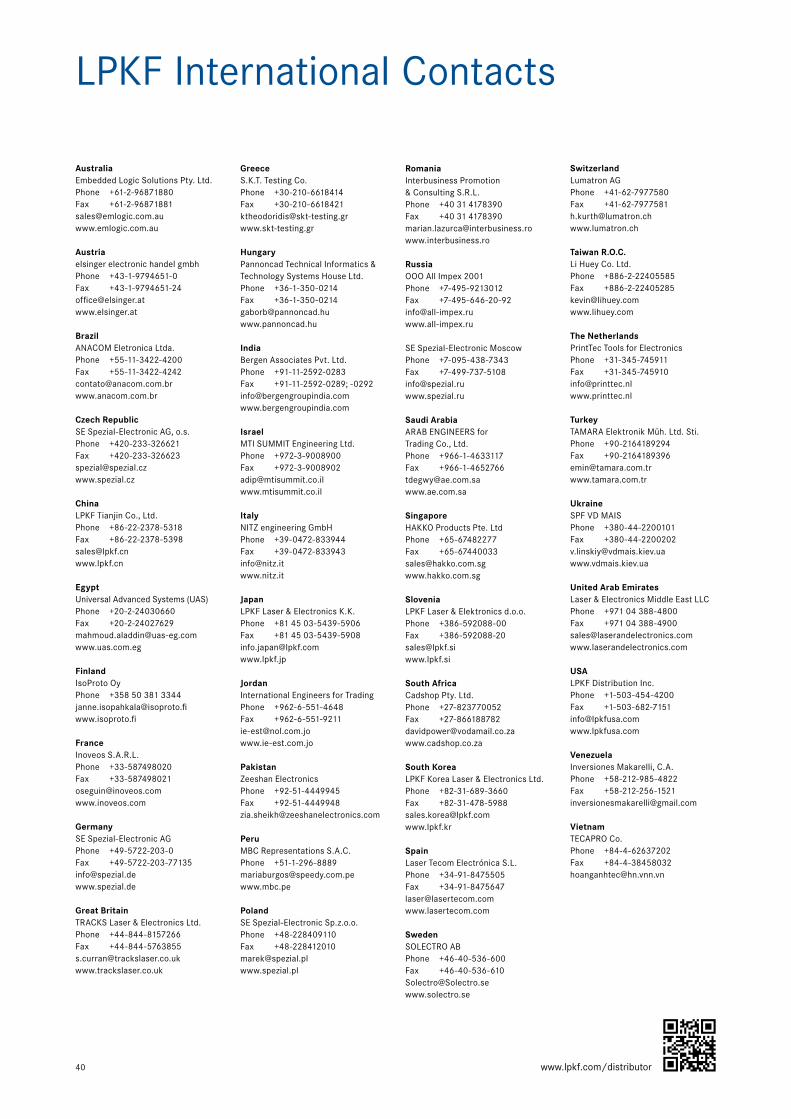
AustraliaEmbedded Logic Solutions Pty. Ltd.Phone +61-2-96871880Fax [email protected]
Austriaelsinger electronic handel gmbhPhone +43-1-9794651-0Fax [email protected]
BrazilANACOM Eletronica Ltda.Phone +55-11-3422-4200Fax [email protected] www.anacom.com.br
Czech RepublicSE Spezial-Electronic AG, o.s.Phone +420-233-326621Fax [email protected]
ChinaLPKF Tianjin Co., Ltd.Phone +86-22-2378-5318Fax [email protected]
EgyptUniversal Advanced Systems (UAS)Phone +20-2-24030660Fax [email protected]
Finland IsoProto OyPhone +358 50 381 [email protected]
France Inoveos S.A.R.L. Phone +33-587498020 Fax +33-587498021 [email protected] www.inoveos.com
GermanySE Spezial-Electronic AGPhone +49-5722-203-0Fax [email protected]
Great BritainTRACKS Laser & Electronics Ltd.Phone +44-844-8157266Fax [email protected]
GreeceS.K.T. Testing Co.Phone +30-210-6618414Fax [email protected]
HungaryPannoncad Technical Informatics & Technology Systems House Ltd.Phone +36-1-350-0214Fax [email protected]
India Bergen Associates Pvt. Ltd. Phone +91-11-2592-0283 Fax +91-11-2592-0289; -0292 [email protected] www.bergengroupindia.com
Israel MTI SUMMIT Engineering Ltd. Phone +972-3-9008900Fax [email protected]
Italy NITZ engineering GmbHPhone +39-0472-833944Fax [email protected]
JapanLPKF Laser & Electronics K.K.Phone +81 45 03-5439-5906Fax +81 45 [email protected]
JordanInternational Engineers for TradingPhone +962-6-551-4648Fax [email protected]
PakistanZeeshan ElectronicsPhone +92-51-4449945Fax [email protected]
PeruMBC Representations S.A.C.Phone [email protected]
Poland SE Spezial-Electronic Sp.z.o.o. Phone +48-228409110 Fax +48-228412010 [email protected] www.spezial.pl
Romania Interbusiness Promotion & Consulting S.R.L. Phone +40 31 4178390 Fax +40 31 4178390 [email protected] www.interbusiness.ro
Russia OOO All Impex 2001 Phone +7-495-9213012Fax [email protected]
SE Spezial-Electronic MoscowPhone +7-095-438-7343 Fax [email protected]
Saudi ArabiaARAB ENGINEERS for Trading Co., Ltd.Phone +966-1-4633117Fax [email protected]
Singapore HAKKO Products Pte. Ltd Phone +65-67482277 Fax +65-67440033 [email protected] www.hakko.com.sg
SloveniaLPKF Laser & Elektronics d.o.o.Phone +386-592088-00Fax [email protected]
South Africa Cadshop Pty. Ltd.Phone +27-823770052Fax [email protected]
South Korea LPKF Korea Laser & Electronics Ltd.Phone +82-31-689-3660Fax [email protected]
Spain Laser Tecom Electrónica S.L.Phone +34-91-8475505Fax [email protected]
SwedenSOLECTRO ABPhone +46-40-536-600Fax [email protected]
SwitzerlandLumatron AGPhone +41-62-7977580Fax [email protected]
Taiwan R.O.C. Li Huey Co. Ltd. Phone +886-2-22405585Fax [email protected]
The NetherlandsPrintTec Tools for ElectronicsPhone +31-345-745911Fax [email protected]
TurkeyTAMARA Elektronik Müh. Ltd. Sti.Phone +90-2164189294Fax [email protected]
UkraineSPF VD MAISPhone +380-44-2200101Fax [email protected]
United Arab Emirates Laser & Electronics Middle East LLCPhone +971 04 388-4800Fax +971 04 [email protected]
USALPKF Distribution Inc.Phone +1-503-454-4200Fax [email protected] VenezuelaInversiones Makarelli, C.A.Phone +58-212-985-4822Fax [email protected]
VietnamTECAPRO Co.Phone +84-4-62637202Fax [email protected]
LPKF International Contacts
www.lpkf.com/distributor
41
Legal Information
Price ListsAny price lists inserted into the catalog or supplied with the catalog are not part of the catalog. All prices are subject to change without notice. Please contact LPKF or an LPKF distributor for the latest offers.
DisclaimerErrors and omissions excepted. Specifications subject to change without notice. The information that LPKF provides in this catalog has been compiled with great care. Although every effort has been made to ensure its accuracy, errors cannot be completely ruled out. LPKF Laser & Electronics AG does not accept any liability for or provide any guarantee of the correctness, accuracy, or completeness of the information provided herein. LPKF reserves the right to change or supplement the information and data provided without prior notice.
Copyright, Trademark, and Patent Information© 2016 LPKF Laser & Electronics AG, Garbsen, Germany. All rights reserved. The contents of this catalog, including images and the catalog design, are protected by copyright and other laws to protect intellectual property. The systems and products of LPKF and their subsidiaries are protected by the applicable German laws and, in some cases, international patents. Product and trade names mentioned in the product catalog are, in some cases, registered trademarks of the respective manufacturers. The LPKF logo, “LPKF ProtoMat,” “LPKF ProConduct,” “CircuitPro,” “ProMask,” “Allegro,” and “SolarQuipment” are registered trademarks of LPKF Laser & Electronics AG.
LPKF Laser & Electronics AG Osteriede 7 30827 Garbsen Deutschland
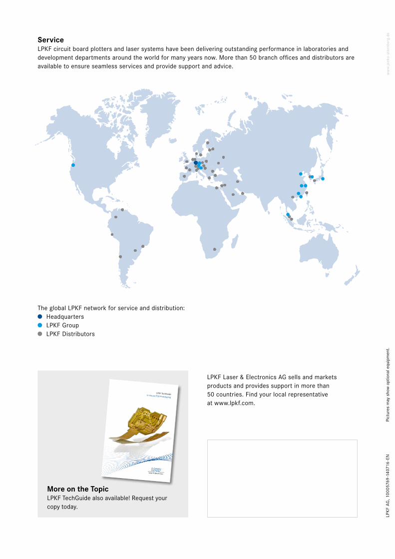
LPKF Laser & Electronics AG sells and markets products and provides support in more than 50 countries. Find your local representative at www.lpkf.com.
Service LPKF circuit board plotters and laser systems have been delivering outstanding performance in laboratories and development departments around the world for many years now. More than 50 branch offices and distributors are available to ensure seamless services and provide support and advice.
More on the TopicLPKF TechGuide also available! Request your copy today.
LPKF TechGuide In-House PCB Prototyping
LPK
F Te
chG
uide
In-H
ouse
PC
B Pr
otot
ypin
g
LPK
F La
ser
& E
lect
roni
cs A
G
LPK
F A
G, ?
????
???-
1506
16-D
E
Bild
er k
önne
n op
tion
ales
Zub
ehör
zei
gen.
w
ww
.jenk
o-s
tern
berg
.de
Service LPKF-Fräsbohrplotter und -Lasersysteme leisten seit Jahren gute Dienste in Laboren und Entwicklungsabteilungen
auf der ganzen Welt. Mehr als 50 Niederlassungen und Distributoren sorgen für reibungslose Serviceleistungen
und stehen mit Tipps und Ratschlägen bereit.
LPKF Laser & Electronics AG vertreibt Produkte und gewährleistet Support in über 50 Ländern. Ihren nächstgelegenen Partner finden Sie unter www.lpkf.com.
Das weltweite LPKF Vetriebs- und Servicenetzwerk: Hauptquartier LPKF-Gruppe LPKF-Vertretungen
Weltweit (LPKF Hauptsitz)LPKF Laser & Electronics AG Osteriede 7 30827 Garbsen DeutschlandTel. +49 (5131) 7095-0 [email protected] www.lpkf.com
NordamerikaLPKF Laser & Electronics North AmericaTel. +1 (503) 454-4200 [email protected] www.lpkfusa.com
China
LPKF Tianjin Co., Ltd.Tel. +86 (22) 2378-5318 [email protected] www.lpkf.com
Hong KongLPKF Laser & Electronics (Hong Kong) Ltd.Tel. +852-2545-4005 [email protected] www.lpkf.com
Japan
LPKF Laser & Electronics K.K. JapanTel. +81 (0) 3 5439 5906 [email protected] www.lpkf.com
Südkorea
LPKF Laser & Electronics Korea Ltd.Tel. +82 (31) 689 3660 [email protected] www.lpkf.com
LPK
F A
G, 1
0005
769
-140
716
-EN
Pict
ures
may
sho
w o
ptio
nal e
quip
men
t.
w
ww
.jenk
o-s
tern
berg
.de
The global LPKF network for service and distribution: Headquarters LPKF Group LPKF Distributors