Embed Size (px)
Citation preview

IN SITU INFRARED SPECTROSCOPY STUDY OF ATOMIC LAYER DEPOSITION OF HIGH-К METAL OXIDE AND
METAL ON PASSIVATED SILICON SURFACES
by
MIN DAI
A dissertation submitted to the
Graduate School-New Brunswick
Rutgers, The State University of New Jersey
In partial fulfillment of the requirements
For the degree of
Doctor of Philosophy
Graduate Program in
Physics and Astronomy
Written under the direction of
Prof. Yves J. Chabal
And approved by
___________________________________
___________________________________
___________________________________
___________________________________
___________________________________
New Brunswick, New Jersey
October, 2008
© 2008
Min Dai
ALL RIGHTS RESERVED
ii
ABSTRACT OF THE DISSERTATION
IN SITU INFRARED SPECTROSCOPY STUDY OF ATOMIC LAYER
DEPOSITION OF HIGH-К METAL OXIDE AND METAL ON
PASSIVATED SILICON SURFACES
By MIN DAI
Dissertation Director:
Prof. Yves J. Chabal
Atomic layer deposition (ALD) is a novel and promising film deposition method for
microelectronics and many other areas with documented commercial success. Notable
advantages include accurate thickness control and high conformality, all of which are
particularly important for deep trenches, porous materials and nanoparticles.
The key elements of ALD including starting surfaces and precursors are investigated
with in situ Fourier transform infrared spectroscopy, using a variety of starting surfaces:
hydrogen-terminated Si (H/Si), oxidized Si, nitrided Si, and self-assembled monolayers
(SAMs) grafted on H/Si surfaces. In particular, the formation of nitrided surfaces using
thermal NH3 reaction with flat and vicinal H/Si(111) is studied and a mechanistic
understanding is achieved with the aid of density functional theory calculation. An
unexpected NH incorporated bridging structure is found at the dihydride step edge. The
properties and stability of methyl and carboxylic groups terminated alkene-based SAMs
grafted to H/Si(111) surface via direct Si-C bonds are also addressed. The carboxylic
iii
groups terminated SAM can be grafted without formation of interfacial SiO2. Moreover,
the use of SiNx and SAM successfully minimizes the interfacial SiO2 during ALD
process.
With a thorough understanding of the starting surfaces, the nature of ALD grown
high-κ metal oxides and metal is studied. Water- and ozone-based ALD of HfO2 and
Al2O3 are investigated mechanistically. Unexpected intermediate species and reaction
pathways are found to depend on ozone partial pressure, such as formate intermediate for
Al2O3 deposition.
La2O3 and Cu deposited by novel precursors, La(iPr-MeAMD)3/D2O and
[Cu(sBu-amd)]2/H2 respectively, are explored in many aspects such as the nature of
precursor gas phase, the ALD temperature window, the film properties, and so on. In all
cases, a mechanistic picture of the surface interaction and film growth is unraveled using
infrared spectroscopy and other complementary techniques, such as Rutherford back
scattering spectroscopy and X-ray photoelectron spectroscopy. Gas phase studies show
that the two precursors are both readily hydrolyzed and highly reactive. ALD-deposited
La2O3 films are of poor quality due to the hygroscopic nature of La2O3, and Cu diffusion
and agglomeration are inferred from the evolution of IR vibrational modes.
iv
Acknowledgements
First and foremost, I would like to express my gratitude to my advisor Prof. Yves J.
Chabal for his invaluable guidance, advice and stimulating discussions as well as
providing great opportunities for me to finish my PhD studies. He is always paying great
attention to my thesis project and actively involved in all my experiments. I learned a lot
from him from his knowledge, patience, consideration and inspiration both in research
and daily life. His enthusiasm for science and work encourages me and shows a great
example for me to continue my studies. I feel really grateful and lucky to have had him as
my advisor.
I would like to thank Dr. Yu Wang and Dr. Ming-Tsung Ho who introduced and
helped me to initiate my thesis project for nitridation and ALD of HfO2. I learned many
experimental skills and FTIR knowledge from them. They are always ready to help. I
would also like to thank Dr. Jinhee Kwon with whom I carried out lots of long
experiments for ALD of La2O3 and ozone based Al2O3, and initiated the study of Cu
ALD and trenched Si. We had many pleasant discussions about our research. She is an
excellent researcher whom I learned a lot from.
I want to thank Dr. Meng Li and Dr. Oliver Seitz. We worked closely together. They
prepared many SAMs samples for me. I learned a lot of interesting chemical knowledge
from them. Oliver also helped me a lot in research and many others things when I was
visiting UTD for 3 months. Also I would like to thank Dr. Mathew Halls for all DFT
theoretical calculations and Dr. Leszek S. Wielunski for RBS Measurements. Thanks
Prof. Roy Gordon for providing La and Cu precursors and insightful information, and Dr.
Uwe Schroeder for trenched samples and SEM pictures. I would thank Dr. Jean-Francois
v
Veyan also. He is extraordinarily helpful in mechanics and many other technical stuffs
making my study much easier. His optimistic attitude towards all things affects me very
much. And thanks Dr. SunKyung Park for her helps at UTD.
There are many other people who helped me very much and I really appreciate. Dr.
David Michalak taught me how to prepare the stepped H/Si and Irinder Chopra told me
how to use AFM. Thanks Norman Lapin, Melissa Stokes, and Nour Nijem, we spent a lot
of time together in the lab. Also thanks Erik Langereis for his excellent 3-month work
with Jinhee and me, and thanks for the help of all my committee members.
vi
Table of Contents
ABSTRACT OF THE DISSERTATION ........................................................................... ii
Acknowledgements............................................................................................................ iv
Table of Contents............................................................................................................... vi
List of Tables...................................................................................................................... ix
List of Illustrations.............................................................................................................. x
List of Frequently Used Abbreviations and Acronyms .................................................... xv
Chapter 1: Introduction ....................................................................................................... 1
1.1 Atomic layer deposition ......................................................................................... 1
1.2 ALD of high-κ metal oxide .................................................................................... 5
1.3 ALD of metal ......................................................................................................... 6
1.4 Overview of the dissertation .................................................................................. 7
Bibliography .............................................................................................................. 10
Chapter 2: Experiment Setup, Substrate Preparation, and Data Analysis......................... 14
2.1 Home made atomic layer deposition system ....................................................... 14
2.2 Sample preparation and FTIR data analysis ........................................................ 17
2.3 Summary .............................................................................................................. 24
Bibliography .............................................................................................................. 24
Chapter 3: Thermal Nitridation of H/Si for ALD ............................................................. 26
3.1 Thermal NH3 nitridation of flat H/Si(111)........................................................... 27
3.2 Thermal NH3 nitridation of vicinal H/Si(111) ..................................................... 31
3.3 HfO2 deposition on nitrided Si(111) surface........................................................ 42
3.4 Summary .............................................................................................................. 47
vii
Bibliography .............................................................................................................. 48
Chapter 4: ALD of Al2O3 and HfO2 with Ozone .............................................................. 52
4.1 TMA gas phase and gas phase reaction ............................................................... 53
4.2 Al2O3 deposition on H/Si(111) using TMA/ozone............................................... 57
4.3 HfO2 deposition using TEMAH/ozone................................................................ 72
4.4 Summary .............................................................................................................. 79
Bibliography .............................................................................................................. 81
Chapter 5: La2O3 and LaxAlyO Growth on H/Si by ALD................................................. 85
5.1 Lanthanum precursor gas phase........................................................................... 85
5.2 ALD of La2O3 on H/Si(111) surface .................................................................... 89
5.3 Miscellany of La(iPr-MeAMD)3 ALD temperature window............................... 98
5.4 ALD of LaxAlyO on H/Si(111) surface .............................................................. 100
5.5 Summary ............................................................................................................ 103
Bibliography ............................................................................................................ 104
Chapter 6: ALD of Cu on Si Surfaces............................................................................. 107
6.1 Precursor properties and the gas phase IR spectrum ......................................... 108
6.2 ALD of Cu on H/Si surface................................................................................ 109
6.3 ALD of Cu on SiO2 .............................................................................................113
6.4 ALD of Cu on SiNx and Al2O3........................................................................... 130
6.5 Other application: deposition of Cu3N............................................................... 136
6.6 Summary ............................................................................................................ 140
Bibliography ............................................................................................................ 141
Chapter 7: SAMs Modification of H/Si, and ALD of Al2O3, HfO2 and Cu on SAMs ... 145
7.1 Stability of the -CH3 and -COOH SAMs........................................................... 147
viii
7.2 ALD of Al2O3 on -COOH SAM ........................................................................ 156
7.3 ALD of HfO2 on -COOH SAM ......................................................................... 166
7.4 ALD of Cu on -COOH SAM ............................................................................. 170
7.5 Summary ............................................................................................................ 173
Bibliography ............................................................................................................ 174
Chapter 8: Summary ....................................................................................................... 178
Appendix: ALD of HfO2 on Trenched H/Si.................................................................... 183
A.1 Thermal stability of H/Si surfaces .................................................................... 184
A.2 HfO2 deposition on trenched H/Si(100)............................................................ 190
A.3 Summary ........................................................................................................... 193
Bibliography ............................................................................................................ 194
Acknowledgment of Previous Publications .................................................................... 196
Curriculum Vita............................................................................................................... 197
ix
List of Tables
Table 2.1 The elements concentration of SiO2/Si(100) surface after RCA cleaning 18Table 2.2 The elements concentration of H/Si(100) 18Table 2.3 Relation between the thickness of SiO2 and integrated area of SiO2 IR
TO/LO modes 23Table 3.1 Calculated PBE/DNP wavenumbers and mode assignments
corresponding to the observed infrared (IR) bands 42Table 4.1 The IR band assignment of TMA gas phase 55Table 5.1 Calculated PBE/DNP wavenumbers and mode assignments
corresponding to the observed infrared (IR) bands based on calculations for the intact La precursor 74
Table 6.1 The thickness of 10 cycles Cu on SiO2 at different temperatures by RBS 125
Table 6.2 The summary XPS results for 10 cycles of Cu on SiO2 at different temperatures. 128
Table 6.3 The summary of element concentration by XPS results for 10 cycles of Cu on SiO2 at 140oC for the fresh sample 128
Table 6.4 The relative O concentration for three fitted O 1s peaks for 10 cycles of Cu on SiO2 at different temperatures 130
Table 6.5 The estimation of pure Cu (Cu0) concentration in all elements for 10 cycles of Cu on SiO2 at different temperatures 130
Table 6.6 The summary of element concentration by XPS results for 10 cycles of Cu on SiNx at 185oC 133
Table 6.7
The summary of element concentration by XPS results for 10 cycles of Cu on Al2O3 at 185oC 136
Table 6.8
The summary of element concentration by XPS results for 20 cycles of reduced Cu3N 140
x
List of Illustrations
Fig 1.1 Ideal ALD process based on self-terminating mechanism 2Fig 1.2 Examples of typical ALD metal precursors 3Fig 1.3 ALD temperature window 4Fig 2.1 Schematic diagram of home made ALD system 14Fig 2.2 Diagram of Nicolet FTIR spectrometer 16Fig 2.3 The absorption spectrum of H/Si(111) referenced to the SiO2 20Fig 2.4 The absorption spectrum of H/Si(100) referenced to the SiO2 22Fig 3.1 Nitridation of flat H/Si (111) referenced to oxide surface 28Fig 3.2 Nitridation of flat H/Si (111) (Spectra are referenced to H/Si (111)
surface) 29Fig 3.3 (a) Opposed NH2+H2 on Si (100) and (b) nitrogen insertion into Si-Si
to form Nx-Si-H 30Fig 3.4 The schematic of (a) monohydride and (b) dihydride stepped H/Si (111)
surfaces 31Fig 3.5 Nitridation of monohydride stepped H/Si(111) 33Fig 3.6 The fitting results of the Si-H stretching modes of monohydride
H/Si(111) 34Fig 3.7 Nitridation of dihydride stepped H/Si(111) 36Fig 3.8 The schematic of H-Si-NH-Si bridging structure due to NH3 interaction
with dihydride 37Fig 3.9 The fitting results of the Si-H stretching modes of dihydride H/Si(111) 38Fig 3.10 Reaction scheme for NH3 reacting at the dihydride H/Si(111) step edge.
Reaction site structures are fully optimized at the PBE/DNP level of theory 39
Fig 3.11 PBE/DNP calculated reaction energy profile for the reaction of NH3 at the dihydride-H/Si(111) surface leading to the NH incorporated step-edge structure 40
Fig 3.12 The structure of TEMAH 43Fig 3.13 ALD reaction scheme of TEMAH and D2O 44Fig 3.14 Differential spectra of first 3 cycles TEMAH/D2O on nitride surface 45Fig 3.15 Absorption spectra up to 20 cycles TEMAH/D2O on nitride surface 46Fig 4.1 Structure of TMA monomer (left) and dimer (right) 53Fig 4.2 The TMA gas phase spectrum and the spectrum after reaction with D2O 54Fig 4.3 The TMA gas phase spectrum and the spectrum after reaction with
ozone 56Fig 4.4 The schematic of adsorbed species on the H/Si after TMA exposure 57Fig 4.5 IR absorption spectrum of H/Si(111) exposed by TMA referenced to
H/Si(111) at 300oC 58
xi
Fig 4.6 Differential FTIR absorption spectra of 10 cycles Al2O3 on H/Si(111) at 300oC 59
Fig 4.7 Absorption spectra of 10 cycles Al2O3 on H/Si(111) at 300oC 60Fig 4.8 Differential FTIR spectra of 20 cycles TMA and ozone deposition on
H/Si(111) at 300oC 62Fig 4.9 (a) Periodic model vibrational density of states (VDOS); and (b) cluster
model IR calculations of each surface structure. 64Fig 4.10 Reaction scheme of formate formation after ozone 66Fig 4.11 A possible pathway to form formate after ozone exposure 67Fig 4.12 Absorption spectra of 20 cycles Al2O3 at 300oC referenced to H/Si(111) 67Fig 4.13 Differential FTIR spectra of 20 cycles TMA and ozone deposition on
H/Si(111) at 300oC with reduced ozone 69Fig 4.14 A possible pathway to form Al-OH after ozone exposure with alcohol
species on the surface 70Fig 4.15 Absorption spectra of 20 cycles Al2O3 at 300oC with reduced ozone
referenced to H/Si(111) 71Fig 4.16 Differential FTIR spectra of 20 cycles TEMAH and ozone deposition
on H/Si(100) 73Fig 4.17 Absorption spectra of 20 cycles HfO2 on and referenced to H/Si(100) at
100oC 74Fig 4.18 Differential FTIR spectra of 20 cycles TEMAH and ozone deposition
on SiNx at 100oC 76Fig 4.19 Absorption spectra of 20 cycles HfO2 on SiNx and referenced to
SiNx(100) at 100oC 77Fig 4.20 Absorption spectra show the annealing of 20 cycles HfO2 on SiNx
referenced to SiNx 78Fig 5.1 Chemical structure of La(iPr-MeAMD)3 precursor and its ball-stick
three dimensional view 86Fig 5.2 FTIR absorption spectrum of gas phase La(iPr-MeAMD)3 and reaction
with D2O 86Fig 5.3 FTIR absorption spectrum of 1st La(iPr-MeAMD)3 on and referenced
to H/Si(111) at 200oC 90Fig 5.4 (a) Absorption spectra of first 3 cycles La(iPr-MeAMD)3+D2O on
H/Si(111) referenced to oxide; (b) Difference spectra of first 3 cycles La(iPr-MeAMD)3+D2O on H/Si(111) 91
Fig 5.5 FTIR absorption spectra of 20 cycles of La precursor and D2O on H/Si(111) at 200oC 92
Fig 5.6 (a) Differential spectra of 19th cycle and 20th cycle La2O3 deposition in the carbonate range; (b) the absorption spectra showing the post annealing of 20 cycles La2O3 in N2 which are reference to the H/Si(111) 94
Fig 5.7 FTIR absorption spectra of 20 cycles of La precursor and D2O on

xii
H/Si(111) at 300oC 96Fig 5.8 Differential spectra of the first 3 cycles of La precursor and D2O on
H/Si(111) at 300oC 97Fig 5.9 Possible decomposition pathways from intact precursor ligand to
cyanamide 98Fig 5.10 Differential spectra of continuous multiple dosing of La precursor on
H/Si(111) at 300oC 99Fig 5.11 Differential spectra of first 4 cycles of LaxAlyO nanolaminate on
H/Si(111) at 300oC 101Fig 5.12 FTIR absorption spectra of 20 cycles of LaxAlyO nanolaminate on
H/Si(111) at 300oC referenced to H/Si(111) 102Fig 6.1 Gas phase FTIR absorption spectrum of the copper precursor
[Cu(sBu-amd)]2 109Fig 6.2 Differential FTIR absorption spectra of [Cu(sBu-amd)]2 on H/Si (100)
surface 110Fig 6.3 (a) Absorption spectra of 10 cycles Cu on H/Si(111) reference to oxide
(left) and (b) the plot of the loss of Si-H vs number cycles (right) 111Fig 6.4 Differential spectra of 10 cycles Cu on H/Si(111) 112Fig 6.5 Differential spectra of the first 3 cycles Cu on oxide 114Fig 6.6 Schematic of Cu precursor and H2 interaction on the SiO2 surface 115Fig 6.7 Absorption spectra of the first 3 cycles Cu on Si oxide 116Fig 6.8 Fitted integrated area of 1010 cm-1 mode 117Fig 6.9 (a) Differential spectra of the first cycle Cu on oxide at different
temperatures. The Cu is referenced to the oxide and the H2 is referenced to the Cu. (b) The absorption spectra of Cu precursor on oxide at different temperatures referenced to oxide 118
Fig 6.10 Schematic of ligand rearrangement on the surface 119Fig 6.11 The ligand behavior after multiple dosing at different temperatures 120Fig 6.12 The differential spectra of the 10th cycle of Cu deposited on SiO2 at
185oC 121Fig 6.13 Results of 10 cycles Cu growth at 140oC 122Fig 6.14 Results of 10 cycles Cu growth at 125oC 124Fig 6.15 The relation between thickness of 1cycle of Cu and growth temperature 125Fig 6.16 XPS results (Cu 2p and C 1s) of 10 cycles Cu on SiO2 at different
temperatures 127Fig 6.17 XPS results (Cu 2p and C 1s) of 10 cycles Cu on SiO2 at 140oC for the
fresh sample 128Fig 6.18 XPS results (O 1s) of 10 cycles Cu on SiO2 at different temperatures 129Fig 6.19 Differential FTIR absorption spectra of 10 cycles 131Fig 6.20 FTIR absorption spectra of 10 cycles Cu on SiNx at 185oC 132Fig 6.21 XPS results (C 1s) of 10 cycles Cu on SiNx at 185oC 133
xiii
Fig 6.22 Differential FTIR absorption spectra of 10 cycles copper ALD on Al2O3 at 185oC 134
Fig 6.23 XPS results (C 1s) of 10 cycles Cu on Al2O3 at 185oC 136Fig 6.24 Differential FTIR absorption spectra of 20 cycles Cu3N on SiO2 at
160oC 137Fig 6.25 FTIR absorption spectra of 20 cycles Cu3N on SiO2 at 160oC 138Fig 6.26 FTIR absorption spectra of 20 cycles Cu3N reduced by forming gas 139Fig 7.1 Area-selective growth of HfO2 146Fig 7.2 The schematic of -CH3 SAM and -COOH SAM 147Fig 7.3 Absorption spectra of (a) -CH3 SAM and (b)-COOH SAM referenced
to H/Si(111) 148Fig 7.4 The annealing results of (a) -CH3 SAM and (b)-COOH SAM in N2
referenced to the fresh SAM surface 151Fig 7.5 The schematic for transformation of carboxyl group to anhydride group 152Fig 7.6 The absorption spectra of (a) -CH3 SAM and (b)-COOH SAM which
are exposed to ozone and referenced to the fresh SAM surface 154Fig 7.7 Differential FTIR absorption spectra of TMA on -COOH SAM surface
at 100oC 156Fig 7.8 Scheme of TMA reacting with the -COOH SAM surface 157Fig 7.9 Differential FTIR absorption spectra of 10 cycles Al2O3 on -COOH
SAM surface deposited at 100oC 158Fig 7.10 Absorption spectra of 10 cycles Al2O3 on SAM deposited at 100oC 160Fig 7.11 Annealing of 10 cycles Al2O3 on -COOH SAM surface in N2 162Fig 7.12 Differential FTIR absorption spectra of 20 cycles Al2O3 by ozone at
100oC on -COOH SAM surface 163Fig 7.13 Absorption spectra of 20 cycles Al2O3 by ozone on SAM 164Fig 7.14 Annealing of 20 cycles Al2O3 by ozone on -COOH SAM surface 165Fig 7.15 Differential FTIR absorption spectra of 10 cycles HfO2 on -COOH
SAM surface at 100oC 167Fig 7.16 Absorption spectra of 10 cycles HfO2 on SAM at 100oC 169Fig 7.17 Annealing of 10 cycles HfO2 on -COOH SAM surface 169Fig 7.18 Differential FTIR absorption spectra of 10 cycles Cu on -COOH SAM
surface at 185oC 171Fig 7.19 Absorption spectra of 10 cycles Cu on SAM referenced to the SAM
surface at 185oC 171Fig 7.20 XP S Cu 2p of 10 cycles Cu on SAM 172Fig A.1 Diagram of a trench capacitor in silicon. 183Fig A.2 Absorption spectra of annealing of flat H/Si(111) at 300oC 184Fig A.3 Absorption spectra of annealing of flat H/Si(100) 185Fig A.4 The structure of trenched sample 186Fig A.5 The absorption spectrum of hydrogen terminated trenched Si(100) 188
xiv
Fig A.6 Absorption spectra of annealing of H-terminated trenched Si surface 189Fig A.7 Absorption spectra of trenched H/Si(100) exposed to TEMAH at 100oC 190Fig A.8 Absorption spectra of trenched H/Si(100) exposed to TEMAH at
various temperatures 191Fig A.9 Absorption spectra of 10 cycles HfO2 on trenched H/Si(100) at 300oC 192Fig A.10 RBS spectrum of 10 cycles HfO2 on trenched H/Si(100) at 300oC 193
xv
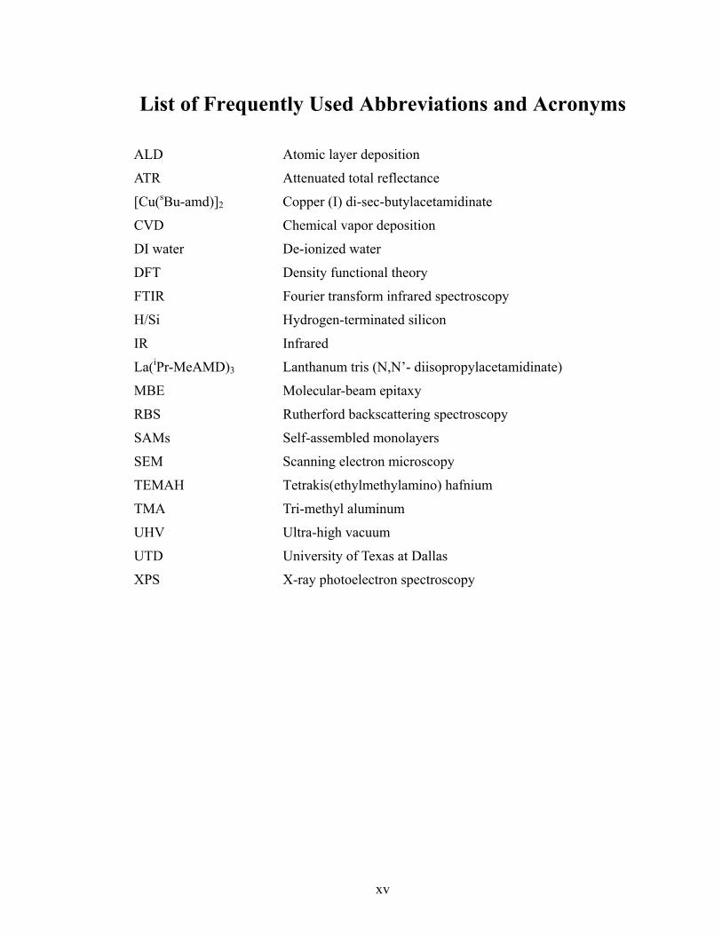
List of Frequently Used Abbreviations and Acronyms
ALD Atomic layer deposition
ATR Attenuated total reflectance
[Cu(sBu-amd)]2 Copper (I) di-sec-butylacetamidinate
CVD Chemical vapor deposition
DI water De-ionized water
DFT Density functional theory
FTIR Fourier transform infrared spectroscopy
H/Si Hydrogen-terminated silicon
IR Infrared
La(iPr-MeAMD)3 Lanthanum tris (N,N’- diisopropylacetamidinate)
MBE Molecular-beam epitaxy
RBS Rutherford backscattering spectroscopy
SAMs Self-assembled monolayers
SEM Scanning electron microscopy
TEMAH Tetrakis(ethylmethylamino) hafnium
TMA Tri-methyl aluminum
UHV Ultra-high vacuum
UTD University of Texas at Dallas
XPS X-ray photoelectron spectroscopy
1
Chapter 1: Introduction
1.1 Atomic layer deposition
Deposition of thin films has great significance in every field with numerous
applications such as in optics, optoelectronics, microelectronics, superconductors,
catalysts, solar energy, and so on. Particularly, the demand of continuous shrinking of
devices for nanotechnology such as in microelectronics and micro-electromechanical
systems (MEMS) requires various thin film deposition methods suitable for different
applications and conditions. Among them, atomic layer deposition (ALD) as a novel
deposition method is attracting more and more attention of both academic and industrial
researchers due to its great advantages in depositing high quality thin films.
ALD was first introduced and realized in 1970s by T. Suntola and co-workers in
Finland to deposit ZnS [1] referred as atomic layer epitaxy at that time. After 30 years of
development, it has become one of the most important methods to deposit thin films.
Compared with other deposition techniques such as CVD, sputtering, MBE, evaporation,
and so on, ALD can be initiated at lower temperature and with more flexible growth
parameters without damaging the surface.
The advantages of ALD include excellent thickness control, high quality (e.g.
pin-hole free films), and highly conformal deposition [2, 3, 4, 5, 6]. Thus, it is a very
good deposition tool for various rough surfaces such as trenches [7, 8], nanowires [9, 10],
nanoporous materials [11, 12], and so on due to its excellent step coverage [13, 14]. For
example, trenches are commonly used for trench capacitor in DRAM to achieved high
capacitance. How to deposit high quality and uniform high-κ insulator/metal gate into
those deep trenches is challenging. For this purpose, ALD is becoming the best choice
because of its good step coverage.
2
ALD has already been utilized to deposit various materials such as metal oxides [6],
metals [15], organic films [16] and nitrides [6] with commercial success. Its applications
include in microelectronic, photonics, MEMS, 3D optoelectronics, photovoltaics,
catalysts, electrolyte fuel cells, and so on [17].
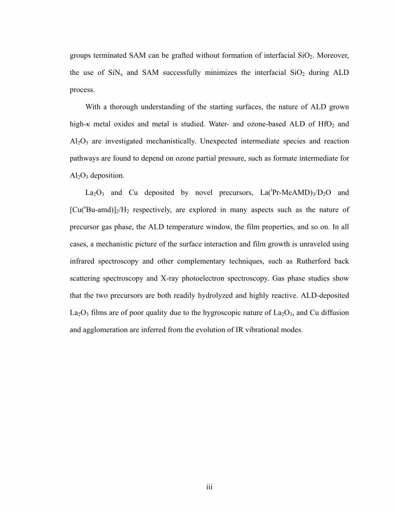
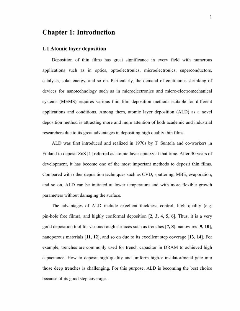
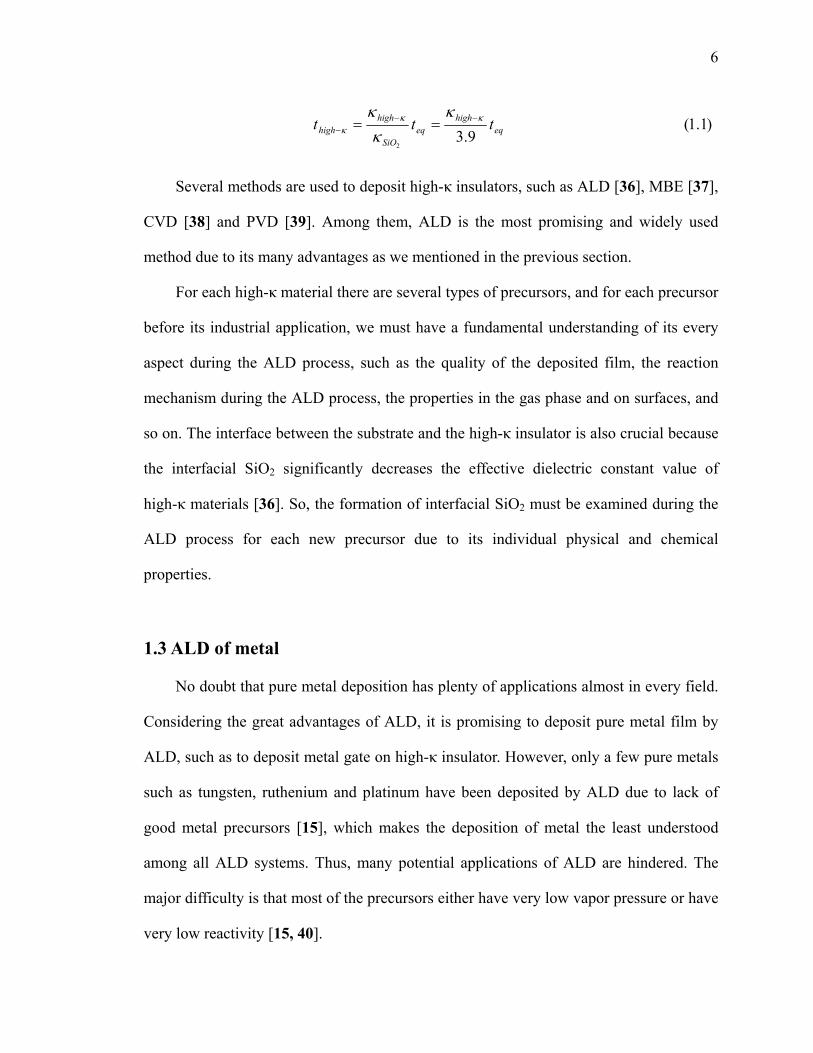
Fig 1.1 Ideal ALD process based on self-terminating mechanism. Precursor A exposure
followed by Precursor B exposure is one cycle. The rest of the precursor is purged away.
ALD is based on self-terminating reaction mechanism [18, 19]. Two precursors, A
and B, are individually and alternatively introduced into the reactor. Each precursor will
not react with itself but react with each other. Thus, the film could be deposited layer by
layer. The thickness of the film is naturally controlled by the number of growth cycles
(one dosing of precursor A with one dosing of B is called one cycle). In this way, a
uniform, pin-hole-free film could be obtained. The schematic procedure of ALD growth
is shown in Fig. 1.1. Starting from a reactive surface, precursor A is carried in and reacts
with the surface until saturating it. Then the rest of the precursor and byproducts are
purged away by inert gas. After that, precursor B is carried in and reacts with the first
layer of adsorbed precursor A on the substrate until saturating the surface, and then again
the rest of the precursor and byproducts are purged away so that one cycle of film is
deposited. By repeating this process, we can deposit the film layer by layer. The thickness
Starting surface Precursor A in Purged by inert gas
Precursor B in
Precursor A Precursor B
Purged by inert gas
3
of the film can be easily controlled by the number of cycles. The typical growth rate is
about 1 Å/cycle. Most ALD processes are thermally activated and plasma has been used
as well to increase the precursor reactivity [20, 21].
In the ideal case, compared with CVD process, the temperature, pressure, and the
precursor pulse length will not affect the ALD growth. So ALD is able to deposit high
quality film at lower temperature with higher parameter tolerance, which is a great
improvement.
However, the real ALD has many critical issues. They can be briefly summarized as
follows:
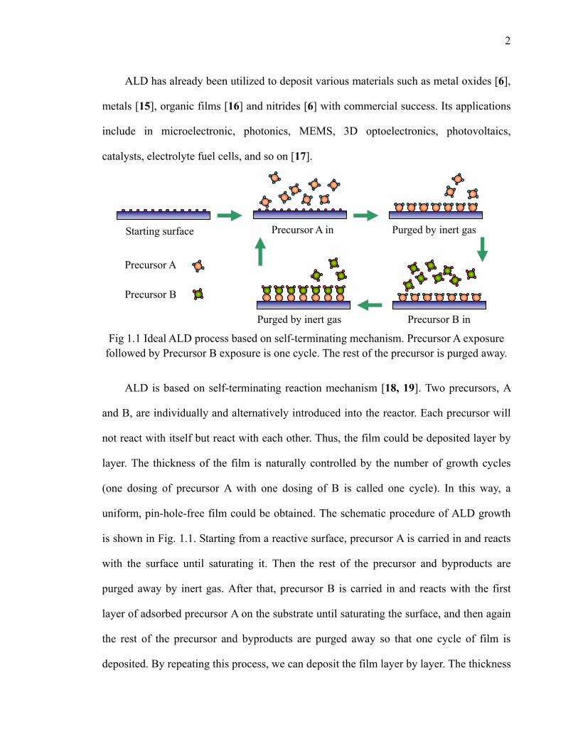
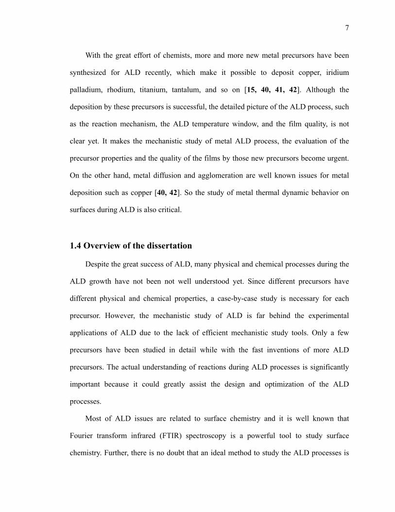
Fig 1.2 Examples of typical ALD metal precursors [22], including metal halides, metal-N,
metal-O, metal-C bonding types and so on.
1) The precursor—precursor is the key element for all ALD process. Several basic
requirements must be satisfied for acceptable ALD precursors [22]. First the precursor
must be highly reactive with both the starting surface and the other precursor previously
attached to the surface but not self-reacting. At the same time, they must be sufficiently
4
volatile at a temperature at which they are thermally stable. A reasonable and
reproducible evaporation rate for the precursors is desired as well. On the other hand, the
byproducts after reaction should not be reactive to or etch the surface and can be easily
purged away. Also, they should not contaminate or damage the ALD reactor.
As for the structures, most ALD metal and metal oxide precursors are halides or
metal organic compounds. Fig 1.2 shows the structures of typical ALD precursors having
been utilized. There are also some pure organic precursors used to deposit organic films
[23]. Usually water or ozone is used as oxidant for metal oxides [24], and H2 [15] or
oxygen [25] is used as reductant for metals. NH3 is also used for nitride deposition [26].
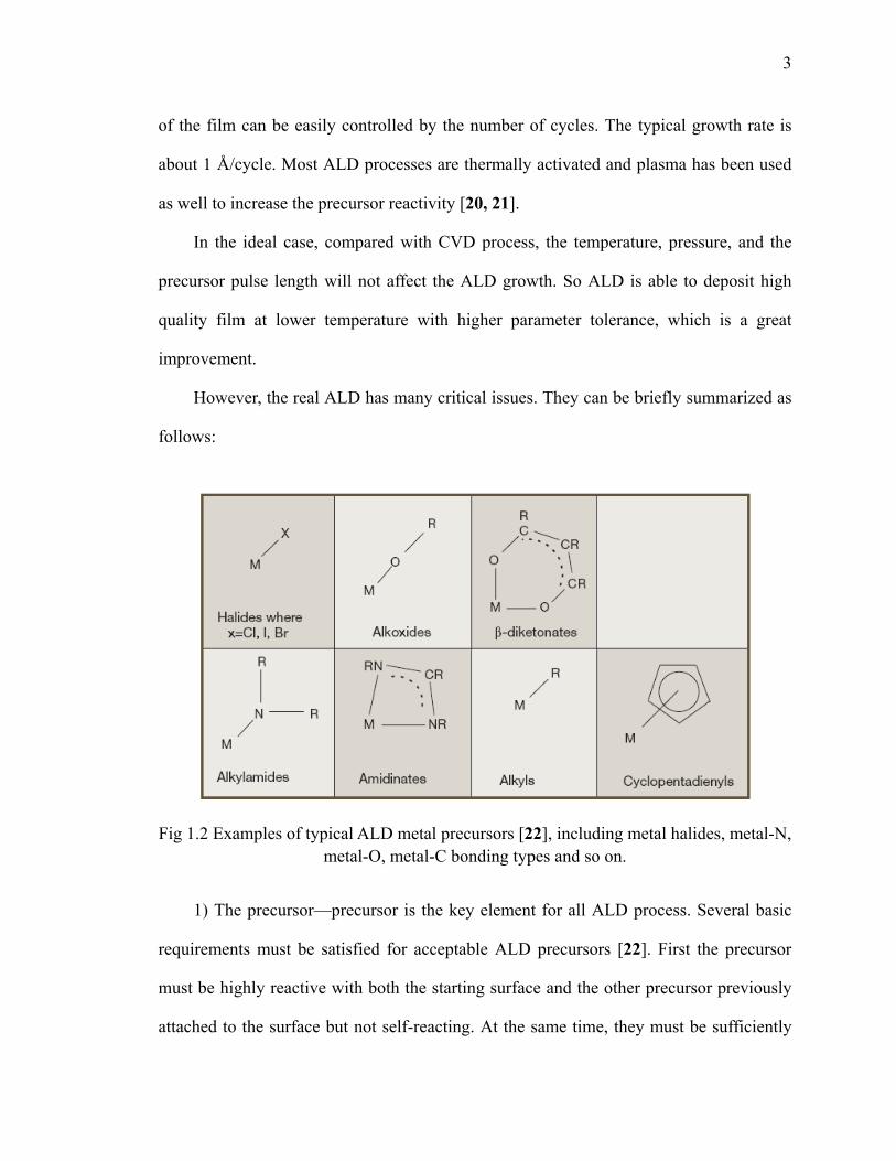
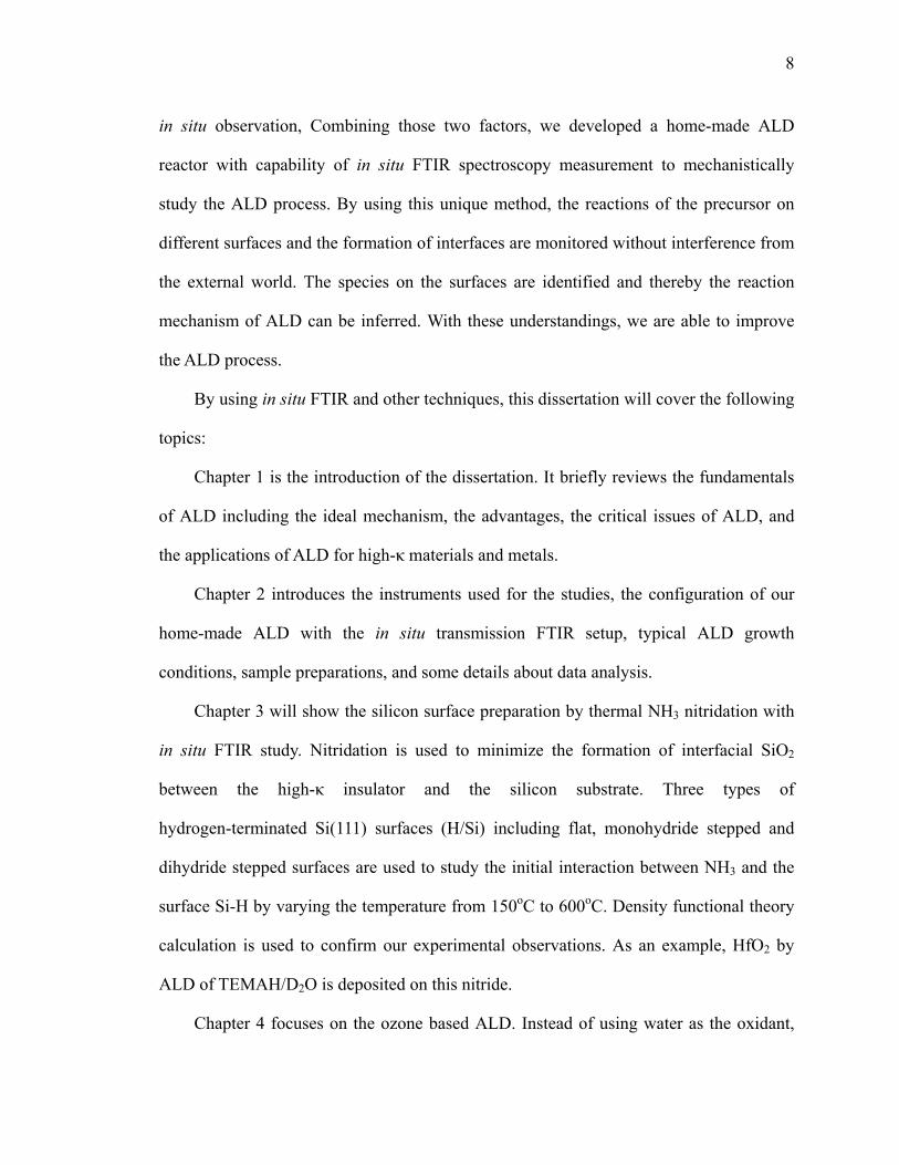
2) The growth temperature—only within the ALD temperature window can we have
real ALD process with a constant growth rate [19]. If the temperature is too low, it may
not initiate the reactions for ALD or may cause insufficient reactions. The physisorption
of the precursor on the surface could also occur, resulting in higher growth rate than
normal. If the temperature is too high, the precursor may decompose to give CVD growth
or may desorb from the surface resulting in lower growth rate. Fig 1.3 shows the relation
between the ALD deposition rate and temperature.
Fig 1.3 ALD temperature window. Only within the ALD window, the growth rate is
constant. Higher or lower temperature will cause unexpected growth rate.
3) The starting surface—ALD cannot deposit the film on any surface. The surface
ALD Window
Temperature
Gro
wth
Rat
e

5
must be chemically reactive enough with the precursor enabling the precursor to
chemically bond to the surface. Otherwise the growth will not take place. If the reactivity
is too low to have saturated growth, it will result in rough film [27]. On the other hand,
the surface must be stable during the transportation and pretreatment before the ALD
process. Various surfaces have been used for different purposes, such as SiO2, H/Si,
nitride, SAMs, graphene, and so on [28, 29, 30, 31, 32].
1.2 ALD of high-κ metal oxide
The transistor--the basic of modern integrated circuit devices, is becoming smaller
and smaller defined as scaling [33]. In transistors, silicon dioxide has been used for
decades as a gate insulator material due to its excellent quality on silicon. Scaling
includes reducing the oxide thickness, junction depth, and depletion width to achieve
high-speed and low-power consumption. It requires the SiO2 gate insulator layer as thin
as possible. However, there is a physical limit for such kind of scaling. When the SiO2
thickness goes down to 10-12 Å, there is no full band-gap structure and it results in
significant leakage current [34, 35]. Thus, alternative insulator materials replacing SiO2
are necessary [36]. High-κ (κ>3.9, κ is the dielectric constant) materials, such as HfO2,
Al2O3, and La2O3, are good candidates to replace SiO2. By using high-κ, the physically
thickness of the high-κ insulator (thigh-κ) would be thicker than that of SiO2 (teq) with
equivalent capacitance, as shown in Eq. 1.1. Therefore, the leakage current is decreased
without impairing the performance of devices. Although high-κ materials can replace the
SiO2, many important issues need to be addressed before the application including band
alignment to silicon, film morphology, thermal stability, mobility of charge carriers,
electrical defects, and so on [36].
6
)1.1(9.3
2
eqhigh
eqSiO
highhigh ttt κκ
κ
κκ
κ −−− ==
Several methods are used to deposit high-κ insulators, such as ALD [36], MBE [37],
CVD [38] and PVD [39]. Among them, ALD is the most promising and widely used
method due to its many advantages as we mentioned in the previous section.
For each high-κ material there are several types of precursors, and for each precursor
before its industrial application, we must have a fundamental understanding of its every
aspect during the ALD process, such as the quality of the deposited film, the reaction
mechanism during the ALD process, the properties in the gas phase and on surfaces, and
so on. The interface between the substrate and the high-κ insulator is also crucial because
the interfacial SiO2 significantly decreases the effective dielectric constant value of
high-κ materials [36]. So, the formation of interfacial SiO2 must be examined during the
ALD process for each new precursor due to its individual physical and chemical
properties.
1.3 ALD of metal
No doubt that pure metal deposition has plenty of applications almost in every field.
Considering the great advantages of ALD, it is promising to deposit pure metal film by
ALD, such as to deposit metal gate on high-κ insulator. However, only a few pure metals
such as tungsten, ruthenium and platinum have been deposited by ALD due to lack of
good metal precursors [15], which makes the deposition of metal the least understood
among all ALD systems. Thus, many potential applications of ALD are hindered. The
major difficulty is that most of the precursors either have very low vapor pressure or have
very low reactivity [15, 40].
7
With the great effort of chemists, more and more new metal precursors have been
synthesized for ALD recently, which make it possible to deposit copper, iridium
palladium, rhodium, titanium, tantalum, and so on [15, 40, 41, 42]. Although the
deposition by these precursors is successful, the detailed picture of the ALD process, such
as the reaction mechanism, the ALD temperature window, and the film quality, is not
clear yet. It makes the mechanistic study of metal ALD process, the evaluation of the
precursor properties and the quality of the films by those new precursors become urgent.
On the other hand, metal diffusion and agglomeration are well known issues for metal
deposition such as copper [40, 42]. So the study of metal thermal dynamic behavior on
surfaces during ALD is also critical.
1.4 Overview of the dissertation
Despite the great success of ALD, many physical and chemical processes during the
ALD growth have not been not well understood yet. Since different precursors have
different physical and chemical properties, a case-by-case study is necessary for each
precursor. However, the mechanistic study of ALD is far behind the experimental
applications of ALD due to the lack of efficient mechanistic study tools. Only a few
precursors have been studied in detail while with the fast inventions of more ALD
precursors. The actual understanding of reactions during ALD processes is significantly
important because it could greatly assist the design and optimization of the ALD
processes.
Most of ALD issues are related to surface chemistry and it is well known that
Fourier transform infrared (FTIR) spectroscopy is a powerful tool to study surface
chemistry. Further, there is no doubt that an ideal method to study the ALD processes is
8
in situ observation, Combining those two factors, we developed a home-made ALD
reactor with capability of in situ FTIR spectroscopy measurement to mechanistically
study the ALD process. By using this unique method, the reactions of the precursor on
different surfaces and the formation of interfaces are monitored without interference from
the external world. The species on the surfaces are identified and thereby the reaction
mechanism of ALD can be inferred. With these understandings, we are able to improve
the ALD process.
By using in situ FTIR and other techniques, this dissertation will cover the following
topics:
Chapter 1 is the introduction of the dissertation. It briefly reviews the fundamentals
of ALD including the ideal mechanism, the advantages, the critical issues of ALD, and
the applications of ALD for high-κ materials and metals.
Chapter 2 introduces the instruments used for the studies, the configuration of our
home-made ALD with the in situ transmission FTIR setup, typical ALD growth
conditions, sample preparations, and some details about data analysis.
Chapter 3 will show the silicon surface preparation by thermal NH3 nitridation with
in situ FTIR study. Nitridation is used to minimize the formation of interfacial SiO2
between the high-κ insulator and the silicon substrate. Three types of
hydrogen-terminated Si(111) surfaces (H/Si) including flat, monohydride stepped and
dihydride stepped surfaces are used to study the initial interaction between NH3 and the
surface Si-H by varying the temperature from 150oC to 600oC. Density functional theory
calculation is used to confirm our experimental observations. As an example, HfO2 by
ALD of TEMAH/D2O is deposited on this nitride.
Chapter 4 focuses on the ozone based ALD. Instead of using water as the oxidant,
9
ozone is used to grow high-κ metal oxides to eliminate trapped water (-OH) inside the
film during the growth. This chapter will show the Al2O3 deposition by TMA and ozone
on H/Si. The gas phase reactions of TMA/H2O and TMA/ozone will be presented. As
another example, HfO2 deposition by TEMAH and ozone on thin silicon nitride as an
oxidation barrier is studied as well.
Chapter 5 will cover the IR mechanistic study of ALD of La2O3 on H/Si surface by a
new precursor--La(iPr-MeAMD)3 [43] and D2O at different temperatures. The precursor
gas phase IR spectra, reactivity, ALD window, and impurities in the film are discussed.
With these understandings, alternating TMA/D2O ALD cycle and La/D2O cycle are used
to deposit LaxAlyO nano-laminate to improve the film quality. Ex situ Rutherford
backscattering spectroscopy (RBS) is used to check the growth rate and film uniformity.
Chapter 6 will show the example of pure copper deposition on various substrates
including H/Si, SiO2, SiNx and Al2O3 by using a new precursor [Cu(sBu-amd)]2 [44]
reduced by H2. Precursor gas phase and the deposition temperature dependence on SiO2
are also studied. The in situ FTIR spectra clearly indicate the copper agglomeration and
diffusion on SiO2 surface, and X-ray photoelectron spectroscopy (XPS) is used to
investigate the contents in the film as well.
Chapter 7 explores the ALD on self-assembled monolayer (SAM) [45] grafted on
H/Si(111) due to its extraordinary electrical properties [46] and potential application for
area-selective ALD growth [47, 48]. As examples, the stability of two kinds of SAMs
including -COOH and -CH3 terminated H/Si(111) is studied. HfO2, Al2O3, and copper are
deposited on -COOH terminated surface which demonstrates that it is a promising
starting surface for ALD.
The appendix chapter presents the preliminary in situ FTIR study of HfO2 deposited
10
on hydrogen-terminated trenched Si(100) surface. The preliminary results of thermal
stability and reactivity of the trenched H/Si surface are shown in this chapter. Then HfO2
deposition is examined by IR spectra and RBS.
Bibliography 1. T. Suntola and J. Antson, Method for producing compound thin films, US Patent (1977), 4, 058, 430. 2. L. Niinistö, M. Nieminen, J. Päiväsaari, J. Niinistö, M. Putkonen and M. Nieminen, Advanced electronic and optoelectronic materials by atomic layer deposition: An overview with special emphasis on recent progress in processing of high-k dielectrics and other oxide materials, Physica Status Solidi (A) 201 (2004), 1443. 3. M. Leskel and R. Mikko, Atomic layer deposition chemistry: Recent developments and future challenges, Angewandte Chemie International Edition 42 (2003), no. 45, 5548. 4. M. Ritala and M. Leskela, Atomic layer epitaxy-a valuable tool for nanotechnology?, Nanotechnology 10 (1999), 19. 5. K.-E. Elers, T. Blomberg, M. Peussa, B. Aitchison, S. Haukka and S. Marcus, Film uniformity in atomic layer deposition, Chemical Vapor Deposition 12 (2006), no. 1, 13. 6. R. L. Puurunen, Surface chemistry of atomic layer deposition: A case study for the trimethylaluminum/water process, Journal of Applied Physics 97 (2005), 121301. 7. R. G. Gordon, D. M. Hausmann, E. Kim and J. Shepard, A kinetic model for step coverage by atomic layer deposition in narrow holes or trenches, Chemical Vapor Deposition 9 (2003), 83. 8. D. Hausmann, J. Becker, S. Wang and R. G.Gordon, Rapid vapor deposition of highly conformal silica nanolaminates, Science 298 (2002), 402. 9. R. Solanki, J. Huo, J. L. Freeouf and B. Miner, Atomic layer deposition of ZnSe/CdSe superlattice nanowires, Applied Physics Letters 81 (2002), no. 20, 3864-3866. 10. Y. Qin, S. M. Lee, A. Pan, U. Gosele and M. Knez, Rayleigh-instability-induced metal nanoparticle chains encapsulated in nanotubes produced by atomic layer deposition, Nano Lett. 8 (2008), no. 1, 114-118. 11. S. O. Kucheyev, J. Biener, Y. M. Wang, T. F. Baumann, K. J. Wu, T. v. Buuren, A. V. Hamza, J. H. Satcher, Jr., J. W. Elam and M. J. Pellin, Atomic layer deposition of ZnO on ultralow-density nanoporous silica aerogel monoliths, Applied Physics Letters 86 (2005), no. 8, 083108. 12. S. P. Adiga, J. W. Elam, M. J. Pellin, C.-C. Shih, C.-M. Shih, S.-J. Lin, Y.-Y. Su, S. D. Gittard, J. Zhang and R. J. Narayan, Nanoporous materials for biomedical devices, Journal of the Minerals, Metals and Materials Society 60 (2008), 26. 13. E. C. John, Chemical methods of thin film deposition: Chemical vapor deposition,
11
atomic layer deposition, and related technologies, Journal of Vacuum Science & Technology A: Vacuum, Surfaces, and Films 21 (2003), no. 5, S88-S95. 14. K. Ja-Yong, A. Ji-Hoon, K. Sang-Won and K. Jin-Hyock, Step coverage modeling of thin films in atomic layer deposition, Journal of Applied Physics 101 (2007), no. 7, 073502. 15. B. S. Lim, A. Rahtu and R. G. Gordon, Atomic layer deposition of transition metals, Nature Materials 2 (2003), 749-754. 16. M. Putkonen, J. Harjuoja, T. Sajavaara and L. Niinistö, Atomic layer deposition of polyimide thin films, Journal of Materials Chemistry 17 (2007), 664-669. 17. http://www.cambridgenanotech.com/ALD-applications.php, Cambridge NanoTech Inc. 18. S. M. George, A. W. Ott and J. W. Klaus, Surface chemistry for atomic layer growth, Journal of Physical Chemistry 100 (1996), no. 31, 13121-13131. 19. T. Suntola, Surface chemistry of materials deposition at atomic layer level, Applied Surface Science 100-101 (1996), 391-398. 20. J. L. van Hemmen, S. B. S. Heil, J. H. Klootwijk, F. Roozeboom, C. J. Hodson, v. d. Sanden and W. M. M. Kessels, Plasma and thermal ALD of Al2O3 in a commercial 200 mm ALD reactor, Journal of the Electrochemical Society 154 (2007), G165-G169. 21. S. B. S. Heil, P. Kudlacek, E. Langereis, R. Engeln, M. C. M. v. d. Sanden and W. M. M. Kessels, In situ reaction mechanism studies of plasma-assisted atomic layer deposition of Al2O3, Applied Physics Letters 89 (2006), no. 13, 131505. 22. C. Musgrave and R. G. Gordon, Precursors for atomic layer deposition of high-k dielectrics, Future Fab International 18 (2005), 126-128. 23. M. Putkonen, J. Harjuoja, T. Sajavaara and L. Niinistö, Atomic layer deposition of polyimide thin films, J. Mater. Chem. 17 (2007), 664. 24. S. K. Kima, C. S. Hwanga, S.-H. K. Parkb and S. J. Yun, Comparison between zno films grown by atomic layer deposition using H2O or O3 as oxidant Thin Solid Films 478 (2005), 103-108. 25. T. Aaltonen, P. Alén, M. Ritala and M. Leskelä, Ruthenium thin films grown by atomic layer deposition, Chemical Vapor Deposition 9 (2003), 45-49. 26. J. W. Elama, M. Schuiskya, J. D. Fergusona and S. M. George, Surface chemistry and film growth during tin atomic layer deposition using TDMAT and NH3, Thin Solid Films 436 (2003), 145-156. 27. M. F. Martin, J. C. Yves, L. G. Martin, D. Annelies, B. Bert, D. W. Glen, H. Mun-Yee, B. O. d. R. Elisa, J. R. B. Israel and C. S. Fernanda, Enhanced initial growth of atomic-layer-deposited metal oxides on hydrogen-terminated silicon, Applied Physics Letters 83 (2003), no. 4, 740-742. 28. X. Wang, S. M. Tabakman and H. Dai, Atomic layer deposition of metal oxides on pristine and functionalized graphene, J. Am. Chem. Soc. 130 (2008), no. 26, 8152-8153. 29. M. T. Ho, Y. Wang, R. T. Brewer, L. S. Wielunski, Y. J. Chabal, N. Moumen and M. Boleslawski, In situ infrared spectroscopy of hafnium oxide growth on
12
hydrogen-terminated silicon surfaces by atomic layer deposition, Applied Physics Letters 87 (2005), no. 13, 133103. 30. B. Busch, O. Pluchery, Y. Chabal, D. Muller, R. Opila, J. Kwo and E. Garfunkel, Materials characterization of alternative gate dielectrics, MRS Bulletin 27 (2002), no. 206-211. 31. R. T. Brewer, M. T. Ho, K. Z. Zhang, L. V. Goncharova, D. G. Starodub, T. Gustafsson, Y. J. Chabal and N. Moumen, Ammonia pretreatment for high-kappa dielectric growth on silicon, Applied Physics Letters 85 (2004), no. 17, 3830-3832. 32. A. S. Killampalli, P. F. Ma and J. R. Engstrom, The reaction of tetrakis(dimethylamido)titanium with self-assembled Alkyltrichlorosilane monolayers possessing -OH, -NH2, and -CH3 terminal groups, J. Am. Chem. Soc. 127 (2005), no. 17, 6300-6310. 33. P. A. Packan, Device physics:Pushing the limits, Science 285 (1999), no. 5436, 2079-2081. 34. D. A. Muller, T. Sorsch, S. Moccio, F. H. Baumann, K. Evans-Lutterodt and G. Timp, The electronic structure at the atomic scale of ultrathin gate oxides, Nature 399 (1999), no. 6738, 758-761. 35. J. B. Neaton, D. A. Muller and N. W. Ashcroft, Electronic properties of the Si/SiO2 interface from first principles, Physical Review Letters 85 (2000), no. 6, 1298. 36. G. D. Wilk, R. M. Wallace and J. M. Anthony, High-k gate dielectrics: Current status and materials properties considerations, Journal of Applied Physics 89 (2001), 5243. 37. D. H. Triyoso, L. H, R. I. Hegde, Z. Yu, K. Moore, J. Grant, B. E. White and P. J. Tobin, Lanthanum aluminate by atomic layer deposition and molecular beam epitaxy, Journal of Vacuum Science & Technology B 23 (2005), 2480. 38. G. Carta, N. El Habra, G. Rossetto, G. Torzo, L. Crociani, M. Natali, P. Zanella, G. Cavinato, V. Matterello, V. Rigato, S. Kaciulis and A. Mezzi, Growth of hafnium dioxide thin films by MOCVD using a new series of cyclopentadienyl hafnium compounds, Chemical Vapor Deposition 13 (2007), 626-632. 39. D. Brassard, M. A. E. Khakani and L. Ouellet, Substrate biasing effect on the electrical properties of magnetron-sputtered high-k titanium silicate thin films, Journal of Applied Physics 102 (2007), no. 3, 034106. 40. Z. Li, A. Rahtu and R. G. Gordon, Atomic layer deposition of ultrathin copper metal films from a liquid copper(I) amidinate precursor, Journal of Electrochemical Society 153 (2006), C787-C794. 41. T. Aaltonen, M. Ritala, Y.-L. Tung, Y. Chi, K. Arstila, K. Meinander and M. Leskelä, Atomic layer deposition of noble metals: Exploration of the low limit of the deposition temperature, Journal of Materials Research 19 (2004), 3353-3358. 42. H. Kim, Atomic layer deposition of metal and nitride thin films: Current research efforts and applications for semiconductor device processing, Journal of Vacuum Science & Technology B: Microelectronics and Nanometer Structures 21 (2003), no. 6, 2231-2261.
13
43. B. S. Lim, A. Rahtu, J.-S. Park and R. G. Gordon, Synthesis and characterization of volatile, thermally stable, reactive transition metal amidinates, Inorganic Chemistry 42 (2003), 7951-7958. 44. Z. Li, S. T. Barry and R. G. Gordon, Synthesis and characterization of Cu(I) amidinates as precursors for atomic layer deposition (ald) of copper metal, Inorganic Chemistry 44 (2005), 1728-1735. 45. A. Ulman, Formation and structure of self-assembled monolayers, Chemical Reviews 96 (1996), 1533-1554. 46. O. Seitz, T. Bocking, A. Salomon, J. J. Gooding and D. Cahen, Importance of monolayer quality for interpreting current transport through organic molecules: Alkyls on oxide-free Si, Langmuir 22 (2006), no. 16, 6915-6922. 47. C. Rong, K. Hyoungsub, C. M. Paul, W. P. David and F. B. Stacey, Achieving area-selective atomic layer deposition on patterned substrates by selective surface modification, Applied Physics Letters 86 (2005), no. 19, 191910. 48. R. Chen and S. Bent, Chemistry for positive pattern transfer using area-selective atomic layer deposition, Advanced Materials 18 (2006), no. 8, 1086-1090.
14
Chapter 2: Experiment Setup, Substrate Preparation,
and Data Analysis
Having been mentioned in the introduction chapter, the deposition is done in our
unique home made atomic layer deposition system. Its most striking feature is that this
system enables in situ transmission infrared spectroscopy study. The detailed information
will be discussed in the following part of this chapter.
2.1 Home made atomic layer deposition system
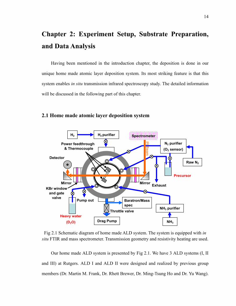
Fig 2.1 Schematic diagram of home made ALD system. The system is equipped with in
situ FTIR and mass spectrometer. Transmission geometry and resistivity heating are used.
Our home made ALD system is presented by Fig 2.1. We have 3 ALD systems (I, II
and III) at Rutgers. ALD I and ALD II were designed and realized by previous group
members (Dr. Martin M. Frank, Dr. Rhett Brewer, Dr. Ming-Tsung Ho and Dr. Yu Wang).
Precursor
Raw N2
Drag Pump
N2 purifier (O2 sensor)
Exhaust
Heavy water (D2O)
Pump out
Power feedthrough & Thermocouple
Throttle valve
Baratron/Mass spec
Detector
H2 purifier H2
NH3
NH3 purifier
Spectrometer
MirrorMirror
IR B
eam
KBr window and gate
valve
15
I was incorporated to finish ALD III and modified ALD II and III afterwards. I was also
involved for the design and realization of the new generation of optimized ALD systems
at UTD. As in Fig 2.1, the main reactor is a UHV chamber denoted by the gray circle in
the diagram. The sample is placed at the center of the chamber and positioned by
tantalum sample holder. DC current passes the sample by applying a DC voltage so that
the sample is heated by the resistivity heating method. In this way, the sample is heated
without touching anything and remains clean, as well as enabling a transmission IR
spectroscopy scheme. The incident angle of the IR can be adjusted by rotating the sample
through a manipulator. Sample temperature is monitored by a thermal couple (welded on
a tantalum clip) clipped to it, and controlled by Eurotherm 2404 controller with HP 6010
DC power supply.
Thermo Nicolet Nexus 6700 and 670 IR spectrometers are used and equipped with
the liquid nitrogen cooled external MCT-B (Mercury Cadmium Telluride) detector which
is favorable for the signal below 1000 cm-1. Typical mid-infrared 400-4000 cm-1 with the
resolution of 4 cm-1 is utilized. The infrared beam comes out from the spectrometer and is
aligned to pass through the center of the sample by using an external parabola mirror.
Then the transmitted beam is reflected and focused again onto the external MCT-B
detector by an ellipsoidal mirror. Transparent KBR windows are mounted to the chamber
to let IR beam enter the chamber and protected by gate valves during the sample
treatment. The detailed and classical introduction of FTIR technique can be found in
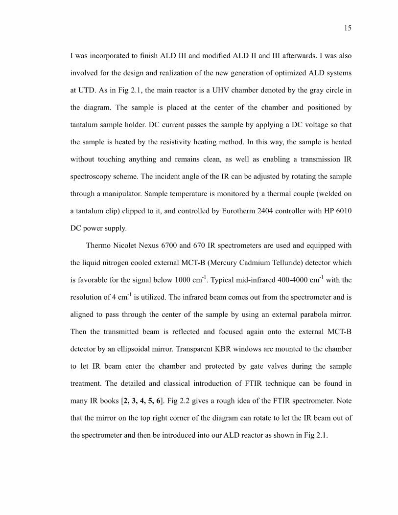
many IR books [2, 3, 4, 5, 6]. Fig 2.2 gives a rough idea of the FTIR spectrometer. Note
that the mirror on the top right corner of the diagram can rotate to let the IR beam out of
the spectrometer and then be introduced into our ALD reactor as shown in Fig 2.1.
16
Fig 2.2 Diagram of Nicolet FTIR spectrometer [1]. The mirror at the top left corner can
rotate to let the IR beam go out to ALD reactor.
The whole system is pumped by an adixen Drytel 1025 dry pump. The MKS 653B
throttle valve is used to control the pumping flow. The base pressure of the system is 10-4
to 10-7 torr. The pressure is monitored by the Baratron Capacitance Manometer. A mass
spectrometer SRS RGA 300 is equipped in the system also. To minimize the adsorbed
water inside, the ALD reactor is baked at 60oC all the time. And therefore, all IR
measurements in this dissertation are performed at a substrate temperature of 60oC.
Because at higher temperature, the excitation of Si electron to conduction band will
reduce the signal intensity, lowest temperature for IR measurement is desired and 60oC is
the lowest temperature in this case.
To ALD reactor
17
1/4 inch stainless steel tubings are used for all gaslines. Gas flow is controlled by
MKS 1479A series mass flow controllers and Swagelok pneumatic valves. N2 gas for
system purging and precursor carrying gas is purified by the Centorr 2A and Oxygon
OG-120M (both with oxygen impurity < 10-6 ppm) purifiers followed by an additional
Aeronex Gate Keeper gas purifier. Ultra high purity (> 99.999%) NH3, H2 and D2 are
introduced into the ALD reactor after purified by Aeronex Gate Keeper gas purifiers.
Ozone are generated by passing O2 (> 99.999%) through the INUSA 5000 ozone
generator. Most important, the ALD metal or metal oxide precursors are equipped in the
system as well, such as D2O and TMA ( for Al2O3) which are both kept at room
temperature, TEMAH kept at ~75oC for HfO2, La(iPr-MeAMD)3 kept at ~130oC for
La2O3, [Cu(sBu-amd)]2 kept at ~95oC for Cu. They will be discussed in detail in later
chapters.
Other instruments are also used in the study, including Rutherford backscattering
spectroscopy (RBS), X-ray photoelectron spectroscopy (XPS)--PHI 5600 ESCA (at
UTD), Atomic Force Microscopy (AFM)--Veeco Dimension 3100 (at UTD), and
Ellipsometry--Horiba Jobin Yvon iHR 320 ellipsometer (at UTD).
2.2 Sample preparation and FTIR data analysis
In our study, double side polished, float-zone grown, and lightly doped (~10 Ω·cm)
Si(111) and Si(100) wafers are used. The sample sized is 1.5 cm×3.8 cm. Before any
further treatment, the sample is first rinsed by acetone, methanol, and deionized water (DI
water, 18.2 MΩ·cm), and then standard RCA [7, 8] (SC1--DI water: H2O2: NH4OH =
4:1:1, SC2--DI water: H2O2: HCl = 4:1:1 at 80oC for 10 min) cleaning is performed
followed by excessive dionized water rinsing. Hydrogen-terminated Si(100) (H/Si)
18
surfaces is achieved by a ~40s HF (~20%) etching after RCA cleaning, and for H/Si(111)
an additional 2.5 min NH4F (~49%) etching [9, 10] is used. In the end, the sample is dried
by N2. Sometimes, instead of RCA cleaning, piranha solution is used for better cleaning
by putting the sample into a mixture of concentrated sulfuric acid and hydrogen peroxide
at the ratio of 3:1 at 90oC for 45-60 min, followed by thoroughly DI-water rinsing. It has
been proven that this method is more efficient than the normal RCA cleaning [7].
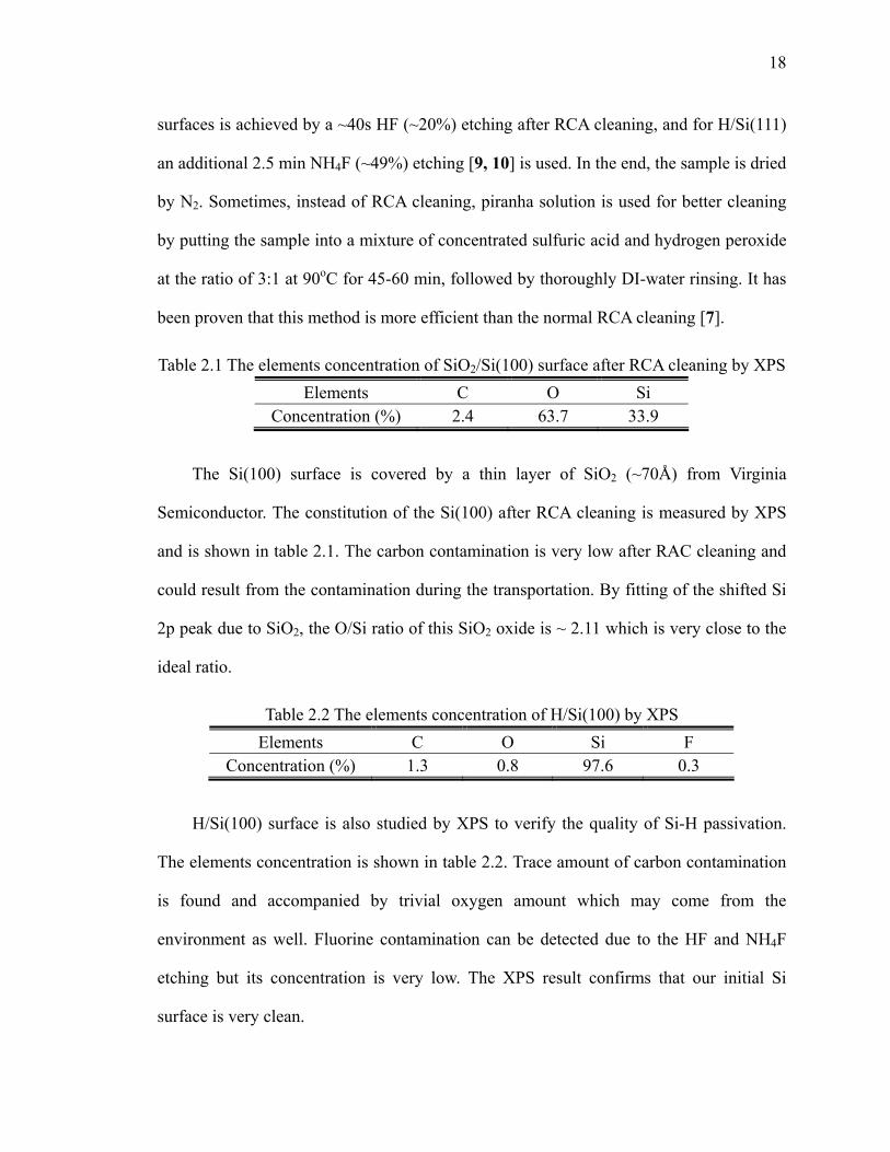
Table 2.1 The elements concentration of SiO2/Si(100) surface after RCA cleaning by XPS Elements C O Si
Concentration (%) 2.4 63.7 33.9
The Si(100) surface is covered by a thin layer of SiO2 (~70Å) from Virginia
Semiconductor. The constitution of the Si(100) after RCA cleaning is measured by XPS
and is shown in table 2.1. The carbon contamination is very low after RAC cleaning and
could result from the contamination during the transportation. By fitting of the shifted Si
2p peak due to SiO2, the O/Si ratio of this SiO2 oxide is ~ 2.11 which is very close to the
ideal ratio.
Table 2.2 The elements concentration of H/Si(100) by XPS Elements C O Si F
Concentration (%) 1.3 0.8 97.6 0.3
H/Si(100) surface is also studied by XPS to verify the quality of Si-H passivation.
The elements concentration is shown in table 2.2. Trace amount of carbon contamination
is found and accompanied by trivial oxygen amount which may come from the
environment as well. Fluorine contamination can be detected due to the HF and NH4F
etching but its concentration is very low. The XPS result confirms that our initial Si
surface is very clean.
19
After the pretreatment, the Si substrate is loaded into the ALD reactor immediately
to carry out IR measurements. FTIR technique is a powerful tool to investigate chemical
bonds on surface, in gas phase, in solids and even in liquid. The typical IR incident angle
used is ~74o (Brewster angle) for highest transmission signal intensity, because the
p-polarized component completely transmits through the sample without any reflection.
Information of both parallel and perpendicular to the surface is achieved at this angle.
Normal incidence (~0o) or close to normal incidence (~20o) is also used to get the
information more parallel to the surface in our study. That is, the incident angle
dependence can identify the orientation of chemical bonds on the surface. The dipole of
the bond perpendicular to the surface can not be observed at normal incidence due to its
non-response to the paralleled electrical field, while both parallel and perpendicular
components can be observed at 74o [11].
To get the absorption spectrum which shows the change in the interface, surface and
film, a reference much be used. The Absorbance (A) can be obtained by using the
following equation:
)()(log
010 ν
νIIA −= (Eq. 2.1)
where I(ν) and Io(ν) are the transmission single beam spectrum of the subject and the
reference, respectively. Thus, all changes of the subject relative to the reference are
exhibited by the absorption spectrum. All positive features in absorbance spectrum
correspond to the formation of new chemical bonds and all negative features correspond
to the removals of the chemical bonds relative to the reference. The frequency, height,
shape, width and integrated area of theses peaks contain many information of a specific
chemical specie, including the chemical bond, dipole, concentration, absorption response,
20
surface morphology, and so on. However, in reality, some artifacts may appear due to the
systematic change in the IR optical bench such as the temperature fluctuation, vibration,
degradation of IR source, strong IR absorption (caused by bulk Si substrate and others),
absorbed contaminations, and so on. All these will affect the single beam and introduce
unwanted artificial bands in the spectrum or distort the baseline of the spectrum.
Furthermore, considering the overlapping of different species’ vibrational modes in the
same frequency range, all make the analysis of IR data more complicated. Although some
effort is needed, IR is a great tool to study surface chemistry.
To reduce some of the systematic error, the spectra in this thesis are taken with a
resolution of 4 cm-1 for 1000 scans per loop and more than 3-4 loops. Only the last three
loops are used and averaged in order to improve signal-to-noise ratio, which is
proportional to the square root of the number of total scans.
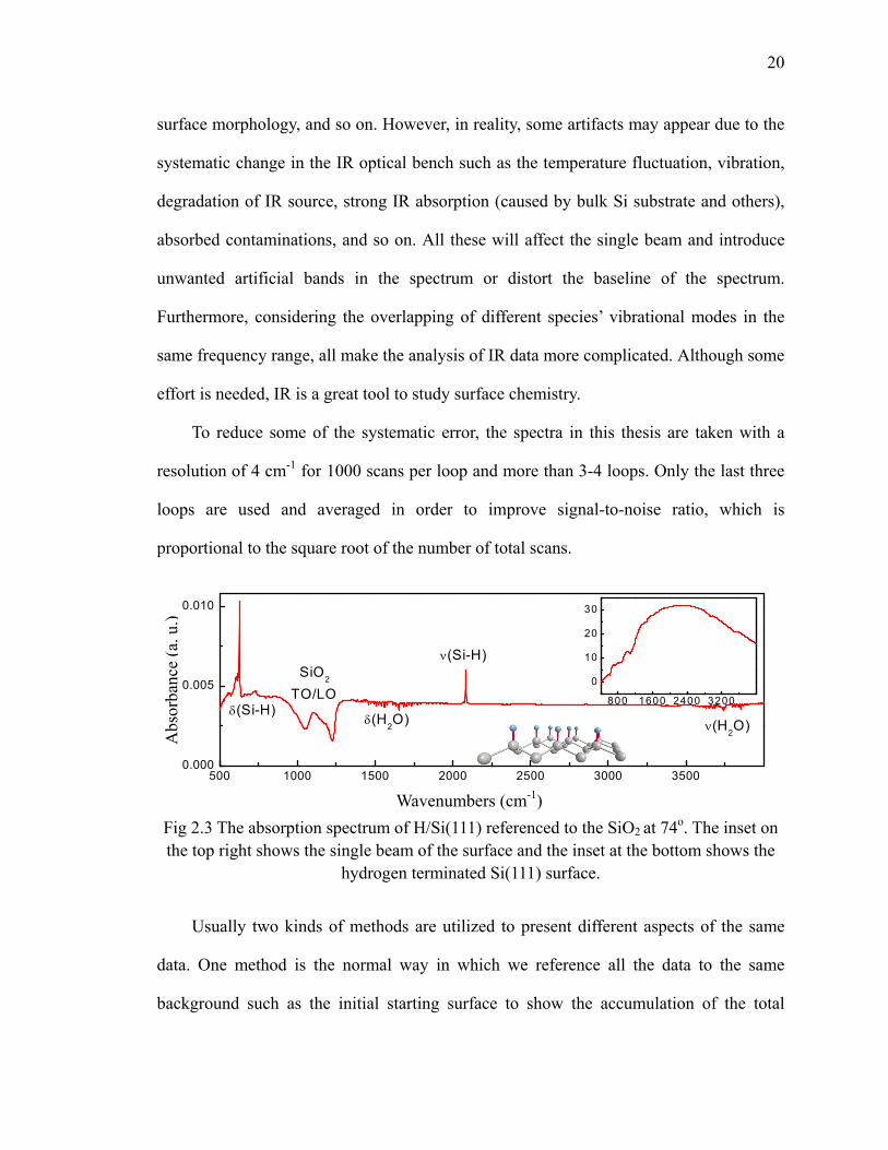
Fig 2.3 The absorption spectrum of H/Si(111) referenced to the SiO2 at 74o. The inset on the top right shows the single beam of the surface and the inset at the bottom shows the
hydrogen terminated Si(111) surface.
Usually two kinds of methods are utilized to present different aspects of the same
data. One method is the normal way in which we reference all the data to the same
background such as the initial starting surface to show the accumulation of the total
500 1000 1500 2000 2500 3000 35000.000
0.005
0.010
SiO2
TO/LOδ(Si-H)
δ(H2O) ν(H2O)
ν(Si-H)
800 1600 2400 3200
0
10
20
30
Wavenumbers (cm-1)
Abs
orba
nce
(a. u
.)
21
changes relative to the background. The other method is called differential spectra where
each spectrum is referenced to the surface after previous treatment. That is, defining B as
the background, and C, D, E…as the subsequent treatments on the surface, the normal
way is to reference C to B, D to B, E to B …, while the differential method is to reference
C to B, D to C, E to D…. Differential spectra are very useful to show the change of the
surface after each treatment.
High sensitivity is achieved by this transmission FTIR geometry. It allows us to
measure chemical species on the surface at monolayer level. As an example, the spectrum
of H/Si(111) surface is presented in Fig 2.3, which is the absorption spectrum of H/Si(111)
referenced to the SiO2/Si(111) surface at 74o. The small inset on the top right of Fig 2.3 is
the single beam of the surface which is used to get the absorption spectrum by Eq. 2.1.
The shape of the single beam is the combination of IR source radiation, detector
sensitivity, beam splitter and KBR window. H/Si(111) is a simple and nearly perfect flat
surface to study the surface chemistry, as shown by the inset at the bottom of Fig 2.3. In
Fig 2.3, the sharp peak at 2083 cm-1 is the stretching mode of Si-H and the peak at 627
cm-1 is Si-H bending mode [12, 13]. The two negative bands at 1050 cm-1 and 1225 cm-1
are assigned to SiO2 TO and LO phonon modes due to the etched SiO2 [14]. The water
from environment outside the ALD chamber along the IR beam path such as in the
spectrometer is featured by the stretching band at 3500-4000 cm-1 and the bending band
at 1300-1900 cm-1. Since the bending band of the water overlaps with most of C, O and N
related modes, water spectrum subtraction is used frequently in the data analysis of this
thesis to remove the water effect.
The other most frequently used surface is H/Si(100) surface which has defects and
more impurities than H/Si(111) surface. H/Si(100) is less stable in the ALD reactor under

22
the N2 purging than the H/Si(111) surface. The thermal stability of these two surfaces will
be shown in the Appendix chapter. The study concludes that H/Si(111) surface is stable
up to 300oC while H/Si(100) surface is stable up to 250oC due to the environmental -OH
group and other oxygen impurities.
500 1000 1500 2000 2500 3000 3500 4000-0.03
-0.02
-0.01
0.00
0.01
ρ(Si-O)
Si-OTO/LO
ν(Si-H)
Fig 2.4 The absorption spectrum of H/Si(100) referenced to the SiO2. The inset shows the detail of the Si-H stretching modes.
The spectrum of H/Si(100) surface which is referenced to oxide at 74o is presented
in Fig 2.4 and the inset is the magnified Si-H range. Different from the flat H/Si(111)
surface, the Si-H stretch has three modes for H/Si(100), which are due to monohydride
(Si-H), dihydride (Si-H2), and trihydride (Si-H3), showing a more complicated surface
morphology [15]. The etching of SiO2 is featured by the negative peaks at 1066 cm-1 and
1254 cm-1, the TO/LO phonon modes. The rocking mode of the SiO2 is observed also
around 810 cm-1. Compared with H/Si(111) surface, the SiO2 TO/LO modes blueshift to
higher frequency, due to the thicker SiO2 layer on the top of silicon [14].
Studies have shown that the SiO2 TO/LO modes blueshift with SiO2 thickness
increasing, and the shift of LO mode is greater than that of TO mode [14]. What’s more,
the integrated area of the two bands is correlated with the thickness of the SiO2 film. In
many cases, the integrated area of the TO/LO modes is used to fast estimate the thickness
2000 2050 2100 2150 2200
0000
0002
0004
0006
Si-H3
Si-H2
Si-H
Abs
orba
nce
(a. u
.)
Wavenumbers (cm-1)

23
of the SiO2. To calibrate it, ellipsometry is used to measure the thickness of SiO2 film and
then the IR integrated area of the corresponding SiO2 TO/LO modes at 74o (incident
angle) is recorded. The ellipsometry is done at the angle of 70o. The results are
summarized in table 2.3. Assuming a linear relation, the fitting gives about 0.047 cm-1/Å
which will be used as a rough estimation standard for SiO2 in the following chapters.
Table 2.3 Relation between the thickness of SiO2 and integrated area of SiO2 IR TO/LO modes
Integrated area (cm-1) 0.47 2.79 0.48 0.52 Thickness (Å) 15.8 66.3 16.9 22.0 Substrate type Si(100) Si(100) Si(111) Si(111)
In addition to the integrated area of SiO2, the integrated area of Si-H stretching
mode is also useful to examine the quality of H/Si after etching. At 74o, the integrated
area of Si-H stretching mode for H/Si(111) is 0.010-0.013 cm-1 and for H/Si(100) the area
is 0.020-0.024 cm-1. The DTGS detector and MCT-B detect have very similar value in
this case.
During all the experiments, after the pretreatment of the surface, the sample is
loaded into the ALD reactor immediately and then is heated to 60oC to take the
background spectra with a small flow of N2 purging (~100 sccm). After that, the next
treatment is performed such as one precursor dosing or thermal annealing, then the
substrate temperature is decreased to 60oC again and spectra are taken at this temperature
with N2 purging. The same process repeats until the whole experiment is done. In
addition, after each ALD precursor dosing, excessive amount of N2 (~500 sccm) is used
to purge the chamber for at least 5min.
24
2.3 Summarys
In this chapter, the schematic layout of our home made ALD system is presented. All
instruments for the experiments are described, such as the FTIR spectrometer, XPS, RBS,
AFM, mass spectrometer, ellipsometer and so on.
The preliminary treatments of the Si surface are discussed including RCA cleaning
and acid etching. XPS results show that the Si surface is clean before loaded into chamber.
H/Si(111) and H/Si(100) surface are discussed by FTIR as examples to show the basic of
IR data analysis.
Bibliography 1. Introduction to Fourier transform infrared spectrometry, Thermal Nicolet (2001). 2. R. T. Conley, Infrared spectroscopy, Allyn and Bacon, Inc. (1972). 3. J. R. Ferraro and L. J. Basile, Fourier transform infrared spectroscopy: Applications to chemical systems, New York: Academic Press (1978). 4. P. R. Griffiths and J. A. D. Haseth, Fourier transform infrared spectrometry, Wiley-Interscience (2007). 5. R. G. Messerschmidt and M. A., Infrared microspectroscopy: Theory and applications, New York: M. Dekker (1988). 6. B. C. Smith, Fundamentals of Fourier transform infrared spectroscopy, CRC Press (1995). 7. G. S. Higashi and Y. J. Chabal, Silicon surface chemical composition and morphology, chapter in handbook of silicon wafer cleaning technology: Science, technology, and applications Werner Kern ed, Noyes Pub., (1993). 8. M. K. Weldon, V. E. Marsico, Y. J. Chabal, D. R. Hamann, S. B. Christman and S. S. E. E. Chaban, Infrared spectroscopy as a probe of fundamental processes in microelectronics: Silicon wafer cleaning and bonding, , Surface Science 368 (1996), 163. 9. G. S. Higashi, R. S. Becker, Y. J. Chabal and A. J. Becker, Comparision of Si(111) surface prepared using aqueous solution of NH4F versus HF, Appl. Phys. Lett. 58 (1991), 1656. 10. M. A. Hines, In search of perfection: Understanding the highly defect-selective chemistry of anisotropic etching, Annu. Rev. Phys. Chem 54 (2003), 29. 11. Y. J. Chabal, Surface infrared spectroscopy, Surf. Sci. Reports 8 (1988), 211. 12. V. A. Burrows, Y. J. Chabal, G. S. Higashi, K. Raghavachari and S. B. Christman, Infrared spectroscopy of Si(111) surfaces after HF treatment: Hydrogen termination and surface morphology, Appl. Phys. Lett. 53 (1988), 998.

25
13. G. S. Higashi, Y. J. Chabal, G. W. Trucks and K. Raghavachari, Ideal hydrogen termination of the Si(111) surface, Appl. Phys. Lett. 56 (1990), 656. 14. K. T. Queeney, N. Herbots, J. M. Shaw, V. Atluri and Y. J. Chabal, Infrared spectroscopic analysis of an ordered Si/SiO2 interface, Appl. Phys. Lett. 84 (2004), 493. 15. Y. J. Chabal, G. S. Higashi, K. Raghavachari and V. A. Burrows, Infrared spectroscopy of Si(111) and Si(100) surfaces after HF treatment: Hydrogen termination and surface morphology, Journal of Vacuum Science & Techonology A 7 (1989), 2104.
26
Chapter 3: Thermal Nitridation of H/Si for ALD
Passivation of semiconductor surface is conveniently realized by terminating surface
dangling bonds with a monovalent atom such as hydrogen, often achieved by a simple
wet chemical process (HF treatment) [1, 2]. However, the real potential of surface
chemical passivation lies in the ability to replace surface hydrogen by multivalent atoms
to form surfaces with tailored properties. While some progress has been made to attach
organic layers on top of hydrogen-terminated surfaces [3, 4, 5], it has been more
challenging to understand and control the incorporation of multivalent atoms, such as
oxygen and nitrogen, within the top surface layer of H-terminated surfaces, partly
because such processes are dominated by defect sites. Silicon nitride (Si3N4) has been studied for years due to its superior thermal,
mechanical and electrical advantages and therefore is utilized in many fields. In
microelectronics, it is an excellent diffusion barrier against oxygen, water and sodium
ions, which make it a very good material as insulator layer and passivation layer [6, 7].
Recently, since the urgent need of high-κ materials to replace silicon dioxide, it also has
been utilized as a barrier to prevent the formation of interfacial silicon oxide between the
silicon substrate and high-κ insulator layer, which will significantly decrease the effective
dielectric constant [8].
Usually silicon nitride can be obtained by CVD, sputtering or plasma nitridation.
However, thermal nitridation by the exposure of silicon to ammonia gas (NH3) is one of
the most promising methods to form the nitride layer because of its high compatibility
with ALD, which is the most widely used method to deposit high-κ materials [9, 10].
Since hydrogen-terminated Si (H/Si) is generally used as the starting surface in order to

27
obtain atomically sharp, oxide free Si and high-κ interface [11], it is also an ideal starting
surface for nitridation. Although extensive studies have focused on the dissociation of
NH3 on Si surface in UHV (non-passivated and reconstructed Si surface) or high
temperature nitridation (above 600°C), and mostly on Si(100) [12, 13, 14, 15, 16, 17, 18,
19], the detailed studies of the initial reaction of NH3 with H/Si surface is few, such as the
NH3 dissociation and nitrogen insertion.
In this chapter, we will discuss the thermal NH3 nitridation of H/Si(111) surface in
the home made ALD reactor by utilizing in situ FTIR. To study the effect of defect sites,
both flat H/Si(111) and vicinal H/Si(111) including monohydride stepped and dihydride
stepped surfaces are introduced. Then by varying substrate temperature from 150oC to
600oC at 25oC step in NH3, the onset of NH3 reaction can be established precisely
through the unambiguous IR spectra and first principle density functional theory (DFT)
calculation.
3.1 Thermal NH3 nitridation of flat H/Si(111)
The preparation of flat H/Si(111) is performed in the same way as described in
Chapter 2, and then the samples are introduced into the ALD chamber immediately.
Thermal nitridation is performed by exposing the Si substrate to NH3 gas [99.999%, with
Aeronex hydride gas purifier (oxygen and non-methane hydrocarbons impurity <1 ppb)]
from 150oC to 600oC at ~ 7-9 torr. The nitridation time is 2 min for each temperature. The
heating and cooling process are both done in NH3 ambient. During the in situ FTIR
measurements, the substrate temperature is kept at 60oC and the incident angle of IR
beam is ~74o (~Brewster angle).
28
2050 2075 2250
2068NxSi-H
Si-H
450oC
500oC475oC
550oC600oC
425oC
300oC
400oC
375oC
350oC
150oC
300oC
60oC
1x10⁻³
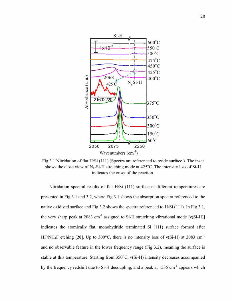
Fig 3.1 Nitridation of flat H/Si (111) (Spectra are referenced to oxide surface.). The inset shows the close view of Nx-Si-H stretching mode at 425oC. The intensity loss of Si-H
indicates the onset of the reaction.
Nitridation spectral results of flat H/Si (111) surface at different temperatures are
presented in Fig 3.1 and 3.2, where Fig 3.1 shows the absorption spectra referenced to the
native oxidized surface and Fig 3.2 shows the spectra referenced to H/Si (111). In Fig 3.1,
the very sharp peak at 2083 cm-1 assigned to Si-H stretching vibrational mode [ν(Si-H)]
indicates the atomically flat, monohydride terminated Si (111) surface formed after
HF/NH4F etching [20]. Up to 300°C, there is no intensity loss of ν(Si-H) at 2083 cm-1
and no observable feature in the lower frequency range (Fig 3.2), meaning the surface is
stable at this temperature. Starting from 350°C, ν(Si-H) intensity decreases accompanied
by the frequency redshift due to Si-H decoupling, and a peak at 1535 cm-1 appears which
Abs
orba
nce
(a. u
.)
21602220
425oC
Wavenumbers (cm-1)
29
is assigned the bending mode [scissor mode, δ(NH2)] of -NH2 species on silicon [15, 17,
21]. These two features indicate initial desorption of Si-H and dissociation of NH3 on the
surface. It can be concluded that NH3 reacting with the H/Si (111) surface is initiated by
replacing the surface hydrogen with Si-NH2, which is in agreement with other
experimental and theoretical studies on Si surface in UHV [13, 15, 18, 22].
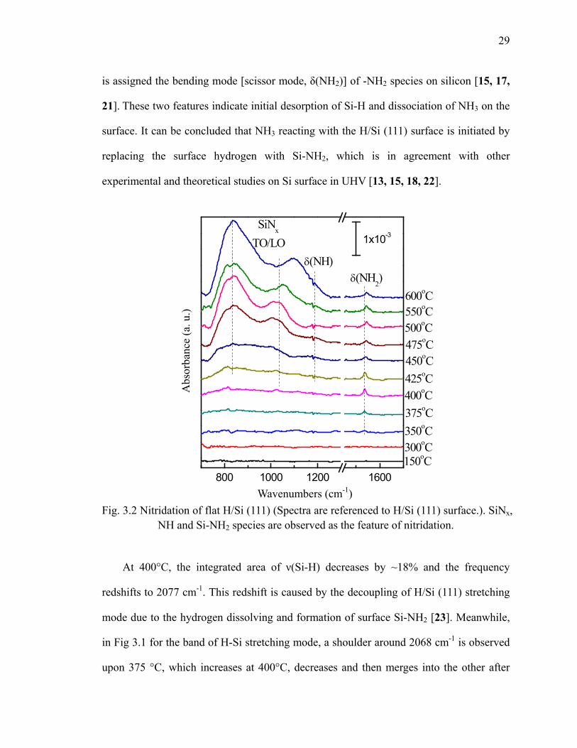
800 1000 1200 1600
SiNx
TO/LOδ(NH)
δ(NH2)
1x10⁻³
450oC
500oC475oC
550oC600oC
425oC
300oC
400oC375oC350oC
150oC
Fig. 3.2 Nitridation of flat H/Si (111) (Spectra are referenced to H/Si (111) surface.). SiNx,
NH and Si-NH2 species are observed as the feature of nitridation.
At 400°C, the integrated area of ν(Si-H) decreases by ~18% and the frequency
redshifts to 2077 cm-1. This redshift is caused by the decoupling of H/Si (111) stretching
mode due to the hydrogen dissolving and formation of surface Si-NH2 [23]. Meanwhile,
in Fig 3.1 for the band of H-Si stretching mode, a shoulder around 2068 cm-1 is observed
upon 375 °C, which increases at 400°C, decreases and then merges into the other after
Wavenumbers (cm-1)
Abs
orba
nce
(a. u
.)
30
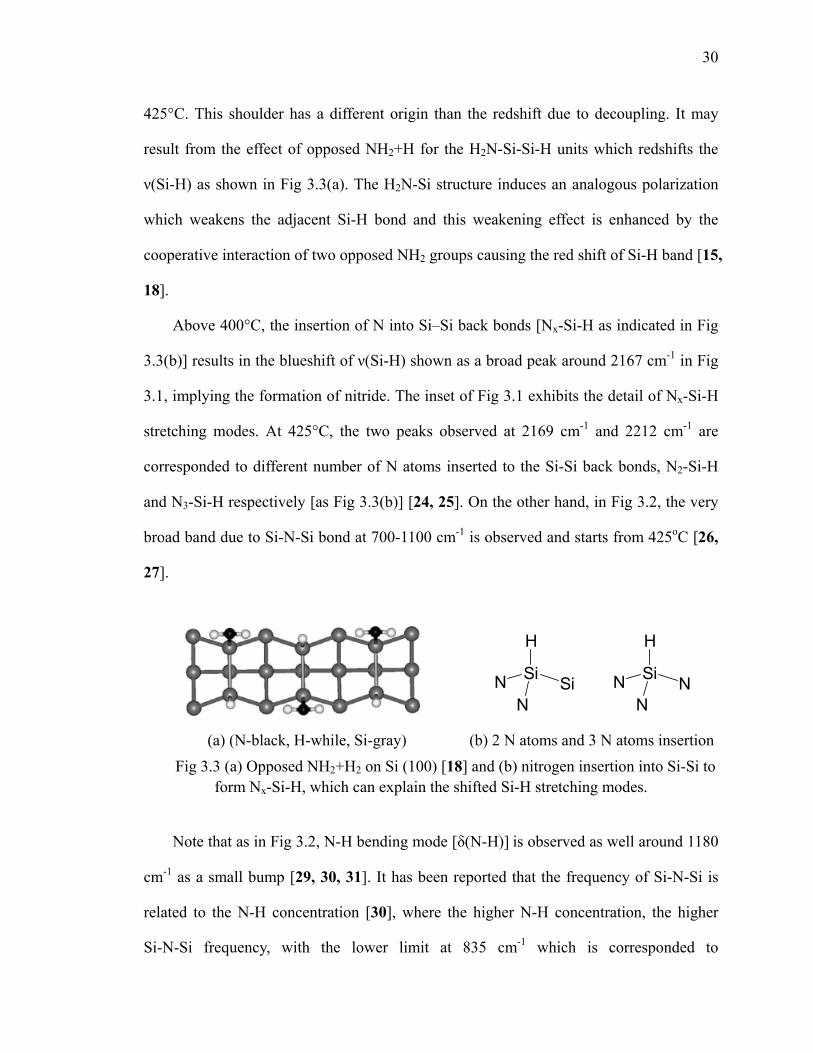
425°C. This shoulder has a different origin than the redshift due to decoupling. It may
result from the effect of opposed NH2+H for the H2N-Si-Si-H units which redshifts the
ν(Si-H) as shown in Fig 3.3(a). The H2N-Si structure induces an analogous polarization
which weakens the adjacent Si-H bond and this weakening effect is enhanced by the
cooperative interaction of two opposed NH2 groups causing the red shift of Si-H band [15,
18].
Above 400°C, the insertion of N into Si–Si back bonds [Nx-Si-H as indicated in Fig
3.3(b)] results in the blueshift of ν(Si-H) shown as a broad peak around 2167 cm-1 in Fig
3.1, implying the formation of nitride. The inset of Fig 3.1 exhibits the detail of Nx-Si-H
stretching modes. At 425°C, the two peaks observed at 2169 cm-1 and 2212 cm-1 are
corresponded to different number of N atoms inserted to the Si-Si back bonds, N2-Si-H
and N3-Si-H respectively [as Fig 3.3(b)] [24, 25]. On the other hand, in Fig 3.2, the very
broad band due to Si-N-Si bond at 700-1100 cm-1 is observed and starts from 425oC [26,
27].
(a) (N-black, H-while, Si-gray) (b) 2 N atoms and 3 N atoms insertion
Fig 3.3 (a) Opposed NH2+H2 on Si (100) [18] and (b) nitrogen insertion into Si-Si to form Nx-Si-H, which can explain the shifted Si-H stretching modes.
Note that as in Fig 3.2, N-H bending mode [δ(N-H)] is observed as well around 1180
cm-1 as a small bump [29, 30, 31]. It has been reported that the frequency of Si-N-Si is
related to the N-H concentration [30], where the higher N-H concentration, the higher
Si-N-Si frequency, with the lower limit at 835 cm-1 which is corresponded to
H
Si
NN Si
H
Si
NN N
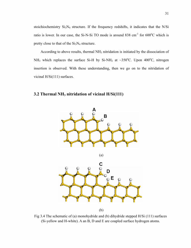
31
stoichiochemistry Si3N4 structure. If the frequency redshifts, it indicates that the N/Si
ratio is lower. In our case, the Si-N-Si TO mode is around 838 cm-1 for 600oC which is
pretty close to that of the Si3N4 structure.
According to above results, thermal NH3 nitridation is initiated by the dissociation of
NH3 which replaces the surface Si-H by Si-NH2 at ~350oC. Upon 400oC, nitrogen
insertion is observed. With these understanding, then we go on to the nitridation of
vicinal H/Si(111) surfaces.
3.2 Thermal NH3 nitridation of vicinal H/Si(111)
(a)
(b)
Fig 3.4 The schematic of (a) monohydride and (b) dihydride stepped H/Si (111) surfaces (Si-yellow and H-white). A an B, D and E are coupled surface hydrogen atoms.
32
Two types of stepped Si (111) wafers with 9o miscut ([112] and [112] ) are utilized
in the nitridation experiments. The stepped hydrogen-terminated Si(111) surfaces are
achieved by 30 seconds HF (~20%) etching at room temperature and an additional 3-4
min NH4F (~49%) etching at 2-4oC [32]. After the samples are immediately introduced
into the ALD chamber, the thermal nitridation is performed by exposing the Si substrate
to NH3 gas and in situ FTIR measurement is carried out at 60oC with the incident angle of
~70o as well, which are the same as flat H/Si(111) surface. Fig 3.4 presents the structural
configuration of the monohydride and dihydride Si(111) surfaces. The one along [112]
direction gives the step Si atoms with one hydrogen bond (monohydride, B), and the
other along [112] direction gives two hydrogen bonds (dihydride, C and D) for the step
Si atoms. Note that for the monohydride surface, the stepped Si-H (B) projects to
between the two Si atoms of the lower terrace and for the dihydride surface the stepped
Si-H (D) projects to the Si-H (E) of the lower terrace.
The nitridation of monohydride surface is show in Fig 3.5(a) and (b), which are
reference to oxide and H/Si respectively. Different from the flat H/Si surface, the spectra
of monohydride surface show three peaks which are located at 2071 cm-1, 2081 cm-1 and
2087 cm-1 [Fig 3.5(a)]. The mode at 2081 cm-1 (C1) is assigned to Si-H terrace stretching
mode, and the other two modes at 2071 cm-1 (C2) and 2087 cm-1 (C3) are associated with
the asymmetric and the symmetric stretching modes resulting from coupled motion of
stepped Si-H and the terrace Si-H next to it [33, 34], as the hydrogen atoms denoted by A
(HA) and B (HB) in Fig 3.4(a).
At 350oC, the total integrated area of Si-H stretching modes slightly decreases
accompanied with the observed δ(NH2) at 1535 cm-1, indicating the starting of NH3
dissociation. Upon 375oC, the Si-H intensity keeps decreasing but due to the overlapping

33
of the terrace and stepped modes, the evolution of each mode cannot be easily
distinguished. To separate those modes, Lorentian curve fitting is carried out for the
results from 300oC to 425oC. The fitted integrated area and peak position for each mode
are shown in Fig 3.6(a), (b) and (c). It can be seen that the integrated area of Si-H terrace
mode is reduced at 350oC and the stepped modes start to vary around 350oC, implying the
surface is attacked by NH3 upon 350oC.
2040 2070 2250Si-H
C3
C2
C1
5x10⁻⁴
Nx-Si-H
450oC
500oC475oC
550oC
425oC
300oC
400oC
375oC
350oC
150oC
60oC
(a) (b)
Fig 3.5 Nitridation of monohydride stepped H/Si(111) (a) referenced to oxide surface. C1, C2, and C3 are Si-H terrace, monohydride asymmetric, and monohydride symmetric
stretching modes, respectively; (b) referenced to H/Si (111) surface. The intensity loss of Si-H indicates the onset of the reaction.
However, it cannot be distinguished that the terrace Si-H is attacked first or the
stepped Si-H reacts first due to their structure similarity. Note that the intensity of terrace
Si-H increases slightly at 375oC and then decreases after 400oC. This slightly increase
800 1000 1200 1600
δ(NH)5x10⁻⁴
450oC
500oC475oC
550oC
425oC
300oC
400oC375oC350oC
150oC
δ(NH2)
SiNx TO/LO
Wavenumbers (cm-1)
Abs
orba
nce
(a. u
.)
Wavenumbers (cm-1)
Abs
orba
nce
(a. u
.)
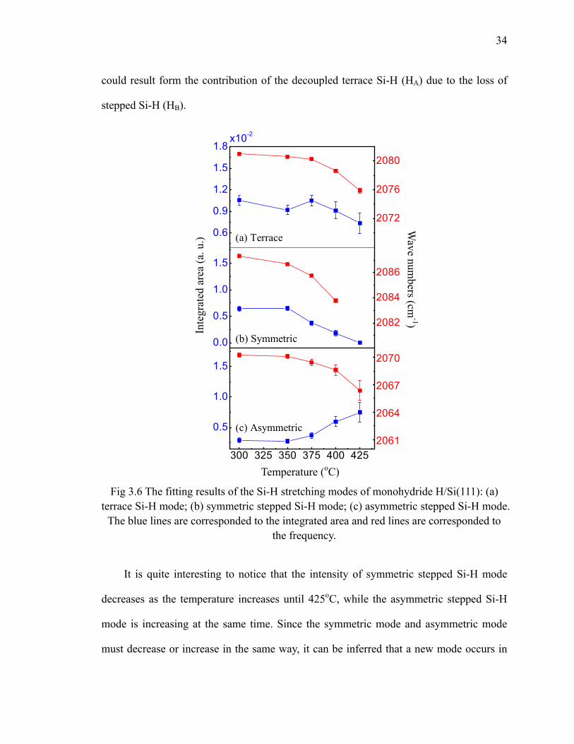
34
could result form the contribution of the decoupled terrace Si-H (HA) due to the loss of
stepped Si-H (HB).
300 325 350 375 400 425
0.5
1.0
1.5
2061
2064
2067
2070
2082
2084
2086
2072
2076
2080
0.0
0.5
1.0
1.5
0.6
0.9
1.2
1.5
1.8
(c) Asymmetric
(b) Symmetric
x10-2
(a) Terrace
Fig 3.6 The fitting results of the Si-H stretching modes of monohydride H/Si(111): (a) terrace Si-H mode; (b) symmetric stepped Si-H mode; (c) asymmetric stepped Si-H mode.
The blue lines are corresponded to the integrated area and red lines are corresponded to the frequency.
It is quite interesting to notice that the intensity of symmetric stepped Si-H mode
decreases as the temperature increases until 425oC, while the asymmetric stepped Si-H
mode is increasing at the same time. Since the symmetric mode and asymmetric mode
must decrease or increase in the same way, it can be inferred that a new mode occurs in
Inte
grat
ed a
rea
(a. u
.)
Wave num
bers (cm-1)
Temperature (oC)

35
the same frequency range which overlaps with the asymmetric mode. Again, this new
mode may be caused by opposed NH2+H for the H2N-Si-Si-H units which redshifts the
terrace stretching mode, as we discussed previously for the nitridation of flat surface in
Fig 3.3(a).
Similar to that of the flat surface, upon 350oC, the observed δ(NH2) at 1535 cm-1
blueshifts to 1544 cm-1 at 550oC as the growing of SiNx layer. The stretching mode of
Nx-Si-H appears around 2167 cm-1 at 400oC [25], accompanied by the Si-N-Si phonon
mode at 700-1100 cm-1 and δ(N-H) at 1180 cm-1, implying the insertion of N into the
Si-Si network. At 550oC, the Nx-Si-H survives and its intensity is about twice of that on
the flat H/Si(111) surface at the same temperature. The broad TO/LO modes of Si-N-Si
centered at 832 cm-1 and 1045 cm-1 are not as sharp as the flat Si(111) surface, indicating
that the nitride on monohydride surface may be rougher and contain more Si than the flat
surface.
Therefore, the nitridation process of monohydride stepped H/Si(111) shows no
difference compared to the flat surface in spite of the presence of steps. For both cases,
the NH3 dissociation and interaction with Si-H ending with Si-NH2 start from ~350oC,
and the nitrogen insertion to Si-Si network is observed at ~400oC.
As for the dihydride surface, the nitridation results are presented in Fig 3.7(a) and
(b), which are reference to oxide and H/Si respectively. As in Fig 3.7(a), the stretching
modes of Si-H are featured by three well separated bands at 2083 cm-1 (C4), 2100 cm-1
(C5) and 2135 cm-1 (C6). The mode at 2083 cm-1 is associated to the terrace Si-H bonds,
and the modes at 2100 cm-1 and 2135 cm-1 are associated to the asymmetric and the
symmetric stretching modes which result from the coupled motion of the stepped Si-H
(HD) and the terrace Si-H (HE) next to it [Fig 3.4(b)] due to the strong steric interaction
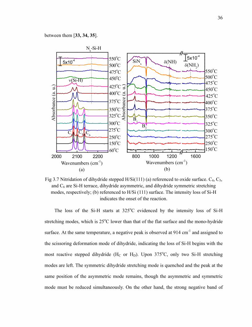
36
between them [33, 34, 35].
2000 2100 2200
Nx-Si-H
ν(Si-H)
C6C5C4
275oC
325oC
250oC
450oC
500oC475oC
550oC
425oC
300oC
400oC375oC
350oC
150oC
60oC
5x10⁻⁴
Fig 3.7 Nitridation of dihydride stepped H/Si(111) (a) referenced to oxide surface. C4, C5, and C6 are Si-H terrace, dihydride asymmetric, and dihydride symmetric stretching modes, respectively; (b) referenced to H/Si (111) surface. The intensity loss of Si-H
indicates the onset of the reaction.
The loss of the Si-H starts at 325oC evidenced by the intensity loss of Si-H
stretching modes, which is 25oC lower than that of the flat surface and the mono-hydride
surface. At the same temperature, a negative peak is observed at 914 cm-1 and assigned to
the scissoring deformation mode of dihydride, indicating the loss of Si-H begins with the
most reactive stepped dihydride (HC or HD). Upon 375oC, only two Si-H stretching
modes are left. The symmetric dihydride stretching mode is quenched and the peak at the
same position of the asymmetric mode remains, though the asymmetric and symmetric
mode must be reduced simultaneously. On the other hand, the strong negative band of
800 1000 1200 1600
δ(NH2)
SiNx δ(NH)
B1
275oC
325oC
250oC
450oC
500oC475oC
550oC
425oC
300oC
400oC375oC350oC
150oC
B2
5x10⁻⁴
Wavenumbers (cm-1) (a)
Abs
orba
nce
(a. u
.)
Wavenumbers (cm-1) (b)
Abs
orba
nce
(a. u
.)

37
dihydride scissoring deformation mode at 914 cm-1 shows that all the surface dihydride is
consumed at 375oC. In addition, a peak at 775 cm-1 starts to appear at 325oC. All these
strongly suggest that a new Si-H mode should be forming during the initial nitridation,
with its stretching mode around the same frequency range as the asymmetric dihydride
stretching mode and accompanied by a bending mode around 775 cm-1. It should also be
note that no δ(NH2) at 1535 cm-1 is observed until 400oC.
Fig 3.8 The schematic of H-Si-NH-Si bridging structure due to NH3 interaction with
dihydride (N-blue, H-white, and Si-yellow). D and E are reacting with NH3, which cause the appearance of new Si-H modes in the spectra: ~2100 cm-1 and 775 cm-1.
All above strongly indicates that dihydride surface should be via a different initial
nitridation mechanism than the flat surface and monohydride surface. We conclude that
NH3 attacks the HD and HE first by forming a H-Si-NH-Si bridging structure due to the
strong steric interaction between these two Si-H bonds, as shown by Fig 3.8. The left
stepped Si-H (HC) in this bridging structure results in the new stretching mode around
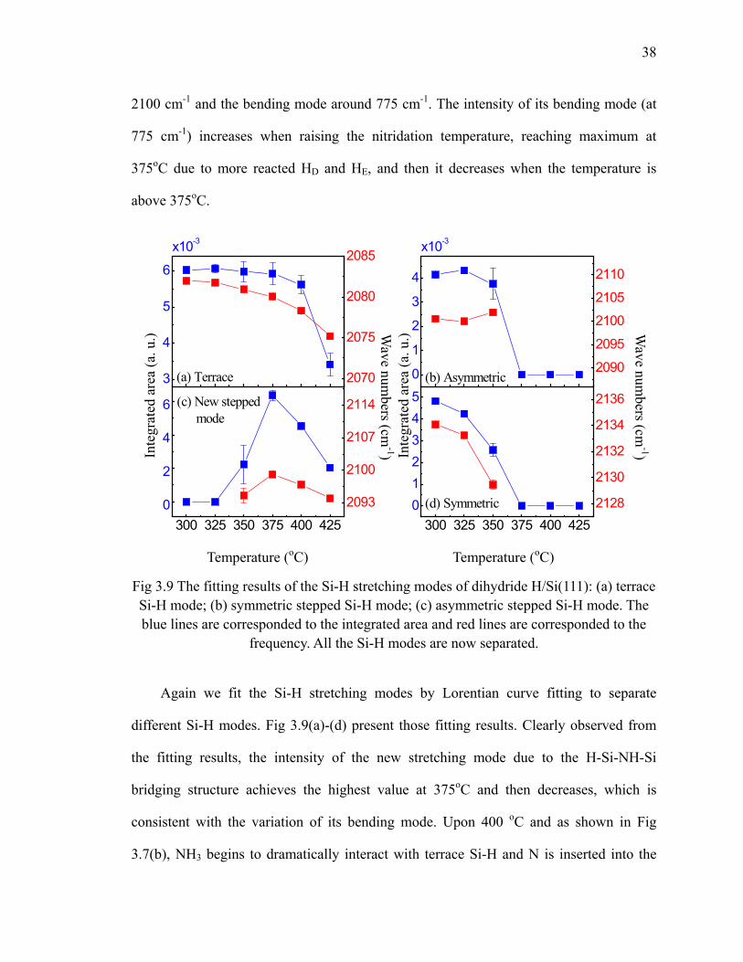
38
2100 cm-1 and the bending mode around 775 cm-1. The intensity of its bending mode (at
775 cm-1) increases when raising the nitridation temperature, reaching maximum at
375oC due to more reacted HD and HE, and then it decreases when the temperature is
above 375oC.
3
4
5
6
2070
2075
2080
2085
2090
2095
2100
2105
2110
2128
2130
2132
2134
2136
2093
2100
2107
2114
x10-3x10⁻³
(c) New stepped mode
(a) Terrace
0
1
2
3
4
(d) Symmetric
(b) Asymmetric
300 325 350 375 400 425012345
300 325 350 375 400 4250
2
4
6
Fig 3.9 The fitting results of the Si-H stretching modes of dihydride H/Si(111): (a) terrace Si-H mode; (b) symmetric stepped Si-H mode; (c) asymmetric stepped Si-H mode. The blue lines are corresponded to the integrated area and red lines are corresponded to the
frequency. All the Si-H modes are now separated.
Again we fit the Si-H stretching modes by Lorentian curve fitting to separate
different Si-H modes. Fig 3.9(a)-(d) present those fitting results. Clearly observed from
the fitting results, the intensity of the new stretching mode due to the H-Si-NH-Si
bridging structure achieves the highest value at 375oC and then decreases, which is
consistent with the variation of its bending mode. Upon 400 oC and as shown in Fig
3.7(b), NH3 begins to dramatically interact with terrace Si-H and N is inserted into the
Inte
grat
ed a
rea
(a. u
.) Wave num
bers (cm-1)
Temperature (oC)
Inte
grat
ed a
rea
(a. u
.) Wave num
bers (cm-1)
Temperature (oC)
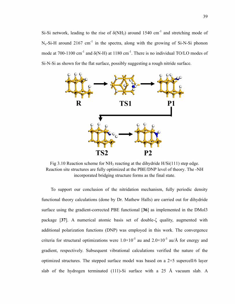
39
R TS1 P1
TS2 P2
Fig 3.10 Reaction scheme for NH3 reacting at the dihydride H/Si(111) step edge. Reaction site structures are fully optimized at the PBE/DNP level of theory. The -NH
incorporated bridging structure forms as the final state.
Si-Si network, leading to the rise of δ(NH2) around 1540 cm-1 and stretching mode of
Nx-Si-H around 2167 cm-1 in the spectra, along with the growing of Si-N-Si phonon
mode at 700-1100 cm-1 and δ(N-H) at 1180 cm-1. There is no individual TO/LO modes of
Si-N-Si as shown for the flat surface, possibly suggesting a rough nitride surface.
To support our conclusion of the nitridation mechanism, fully periodic density
functional theory calculations (done by Dr. Mathew Halls) are carried out for dihydride
surface using the gradient-corrected PBE functional [36] as implemented in the DMol3
package [37]. A numerical atomic basis set of double-ζ quality, augmented with
additional polarization functions (DNP) was employed in this work. The convergence
criteria for structural optimizations were 1.0×10⁻⁵ au and 2.0×10⁻³ au/Å for energy and
gradient, respectively. Subsequent vibrational calculations verified the nature of the
optimized structures. The stepped surface model was based on a 2×5 supercell/6 layer
slab of the hydrogen terminated (111)-Si surface with a 25 Å vacuum slab. A
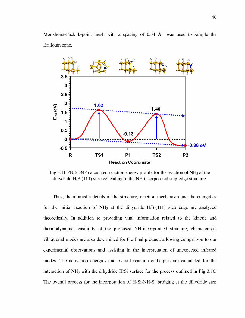
40
-0.5
0
0.5
1
1.5
2
2.5
3
3.5
R TS1 P1 TS2 P2Reaction Coordinate
E Rel
(eV) 1.62
1.40
-0.13
-0.36 eV
Fig 3.11 PBE/DNP calculated reaction energy profile for the reaction of NH3 at the
dihydride-H/Si(111) surface leading to the NH incorporated step-edge structure.
Monkhorst-Pack k-point mesh with a spacing of 0.04 Å-1 was used to sample the
Brillouin zone.
Thus, the atomistic details of the structure, reaction mechanism and the energetics
for the initial reaction of NH3 at the dihydride H/Si(111) step edge are analyzed
theoretically. In addition to providing vital information related to the kinetic and
thermodynamic feasibility of the proposed NH-incorporated structure, characteristic
vibrational modes are also determined for the final product, allowing comparison to our
experimental observations and assisting in the interpretation of unexpected infrared
modes. The activation energies and overall reaction enthalpies are calculated for the
interaction of NH3 with the dihydride H/Si surface for the process outlined in Fig 3.10.
The overall process for the incorporation of H-Si-NH-Si bridging at the dihydride step

41
edge involves two reaction steps: 1) the initial reaction of NH3 at the lower step edge (HD)
Si-H (R) forming a step-edge -NH2 species (P1), and 2) the subsequent reaction of the
step-edge -NH2 (P1) with the adjacent lower terrace Si-H (HE), producing the final NH
incorporated step-edge product (P2). The critical point structures for this process are
labelled and shown in Fig 3.10 and Fig 3.11 (top). Reactant, product and linking
transition state structures were fully optimized and verified by subsequent frequency
analyses.
The reaction energy profile for the step-edge nitridation is shown in Fig 3.11
(energies denoted by ). As presented there, as NH3 interacts with the step-edge Si-H
reaction site, the system proceeds through a transition state (TS1) having an energy 1.62
eV higher than the initial separated reactants (R). Structurally, the transition state has
elongated Si-H, N-H and Si-N, H-H distances relative to their initial and final values,
respectively, consistent with transitional nature of these bonds. From the TS1 state the
system evolves forming the step-edge-NH2 (P1) species, with the loss of H2. The
formation of the P1 intermediate product is calculated to be exothermic by 0.13 eV. From
the -NH2 P1 structure the system can react further to produce the final NH incorporated
step-edge product (P2). As shown in Fig 3.11, the second step-edge reaction step has a
classical barrier height of 1.40 eV. The second transition structure has bond lengths
consistent with the reaction path linking the P1 and P2 structures. The formation of the
final NH bridging structure with loss of H2 is predicted to be exothermic by 0.36 eV.
The density functional theory results presented here indicate that the initial reaction
of NH3 at the stepped edge of dihydride surface to form the unique NH incorporated
step-edge structure is thermodynamically favourable overall. The energies of both the
intermediate product (P1) and the final step-edge product (P2) are lower than the starting
42
reactants, with the final P2 product being most stable. The initial reaction step is found to
dominate the kinetics of the process, with the activation energy for the second reaction
step being smaller (TS2) than that for the initial reaction (TS1). These results reveal that
nitridation of the stepped dihydride surface is energetically favourable and the initial NH3
step-edge nucleation readily leads to formation of the final products.
Table 3.1 Calculated PBE/DNP wavenumbers and mode assignments corresponding to the observed infrared (IR) bands
Calculateda (cm-1) Observed IR (cm-1) Assignment 894 914 Si-H2 scissoring deformation 2134 2100 Bridged H-Si-(NH-Si) stretching 772 775 Bridged H-Si-(NH-Si) bending 1165 N/A N-H bending 856 N/A Si-N stretching
a PBE/DNP calculated harmonic frequencies.
Following the analysis of the mechanism and energetics for the proposed initial
step-edge nitridation reaction, the theoretically predicted properties of the final P2
structure perfectly match our experimental observations. Both the ~ 2100 cm-1 and 775
cm-1 vibrations are associated with the remaining step-edge Si-H (HC) after bridging NH
incorporation to form the H-Si-NH-Si structure. The remaining Si-H (HC) stretching
mode and its bending mode for the step-edge H-Si-NH-Si structure are in excellent
agreement with the observed infrared bands as shown in table 3.1 (calcd (υ/δ): 2134/772
cm-1; expt (υ/δ): 2100/775 cm-1).
3.3 HfO2 deposition on nitrided Si(111) surface Thermal NH3 nitridation of silicon has shown advantage as an oxygen barrier in
ALD of Al2O3 [8]. Based on the nitride achieved in the previous discussion, HfO2 is
deposited on it to demonstrate its application for ALD. Known as a high-κ metal oxide
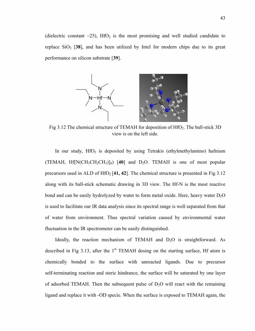
43
(dielectric constant ~25), HfO2 is the most promising and well studied candidate to
replace SiO2 [38], and has been utilized by Intel for modern chips due to its great
performance on silicon substrate [39].
Hf N
N
N
N
Fig 3.12 The chemical structure of TEMAH for deposition of HfO2. The ball-stick 3D
view is on the left side.
In our study, HfO2 is deposited by using Tetrakis (ethylmethylamino) hafnium
(TEMAH, Hf[N(CH3CH2CH3)]4) [40] and D2O. TEMAH is one of most popular
precursors used in ALD of HfO2 [41, 42]. The chemical structure is presented in Fig 3.12
along with its ball-stick schematic drawing in 3D view. The Hf-N is the most reactive
bond and can be easily hydrolyzed by water to form metal oxide. Here, heavy water D2O
is used to facilitate our IR data analysis since its spectral range is well separated from that
of water from environment. Thus spectral variation caused by environmental water
fluctuation in the IR spectrometer can be easily distinguished.
Ideally, the reaction mechanism of TEMAH and D2O is straightforward. As
described in Fig 3.13, after the 1st TEMAH dosing on the starting surface, Hf atom is
chemically bonded to the surface with unreacted ligands. Due to precursor
self-terminating reaction and steric hindrance, the surface will be saturated by one layer
of adsorbed TEMAH. Then the subsequent pulse of D2O will react with the remaining
ligand and replace it with -OD specie. When the surface is exposed to TEMAH again, the
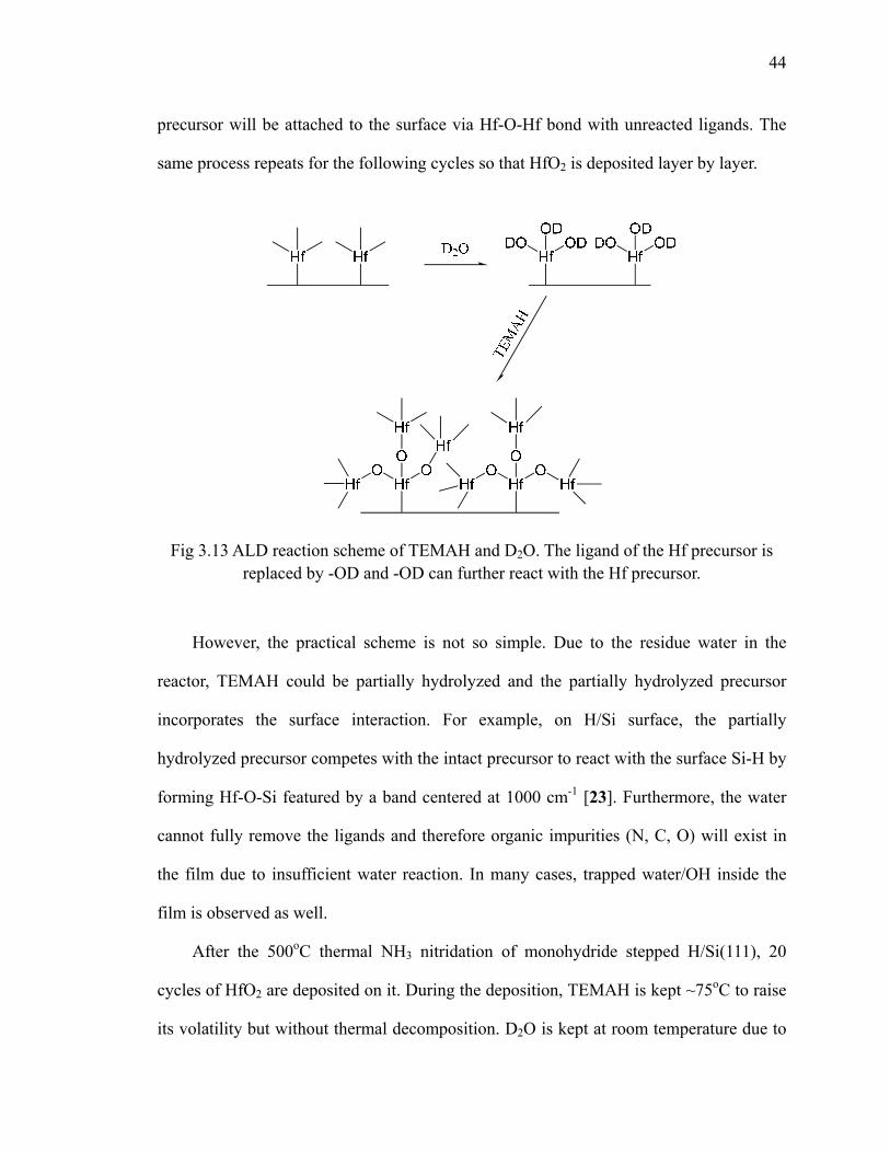
44
precursor will be attached to the surface via Hf-O-Hf bond with unreacted ligands. The
same process repeats for the following cycles so that HfO2 is deposited layer by layer.
Fig 3.13 ALD reaction scheme of TEMAH and D2O. The ligand of the Hf precursor is replaced by -OD and -OD can further react with the Hf precursor.
However, the practical scheme is not so simple. Due to the residue water in the
reactor, TEMAH could be partially hydrolyzed and the partially hydrolyzed precursor
incorporates the surface interaction. For example, on H/Si surface, the partially
hydrolyzed precursor competes with the intact precursor to react with the surface Si-H by
forming Hf-O-Si featured by a band centered at 1000 cm-1 [23]. Furthermore, the water
cannot fully remove the ligands and therefore organic impurities (N, C, O) will exist in
the film due to insufficient water reaction. In many cases, trapped water/OH inside the
film is observed as well.
After the 500oC thermal NH3 nitridation of monohydride stepped H/Si(111), 20
cycles of HfO2 are deposited on it. During the deposition, TEMAH is kept ~75oC to raise
its volatility but without thermal decomposition. D2O is kept at room temperature due to
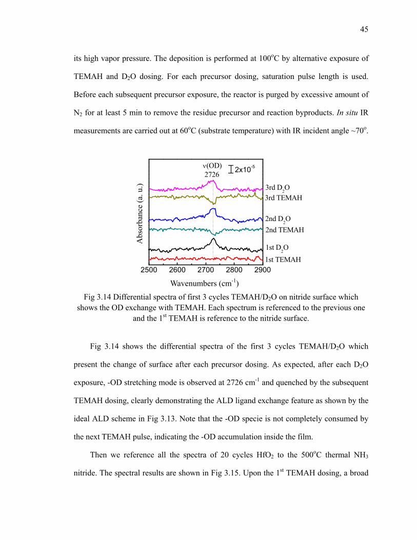
45
its high vapor pressure. The deposition is performed at 100oC by alternative exposure of
TEMAH and D2O dosing. For each precursor dosing, saturation pulse length is used.
Before each subsequent precursor exposure, the reactor is purged by excessive amount of
N2 for at least 5 min to remove the residue precursor and reaction byproducts. In situ IR
measurements are carried out at 60oC (substrate temperature) with IR incident angle ~70o.
2500 2600 2700 2800 29001st TEMAH1st D2O
2x10⁻⁵ν(OD) 2726
3rd TEMAH
2nd D2O2nd TEMAH
3rd D2O
Fig 3.14 Differential spectra of first 3 cycles TEMAH/D2O on nitride surface which shows the OD exchange with TEMAH. Each spectrum is referenced to the previous one
and the 1st TEMAH is reference to the nitride surface.
Fig 3.14 shows the differential spectra of the first 3 cycles TEMAH/D2O which
present the change of surface after each precursor dosing. As expected, after each D2O
exposure, -OD stretching mode is observed at 2726 cm-1 and quenched by the subsequent
TEMAH dosing, clearly demonstrating the ALD ligand exchange feature as shown by the
ideal ALD scheme in Fig 3.13. Note that the -OD specie is not completely consumed by
the next TEMAH pulse, indicating the -OD accumulation inside the film.
Then we reference all the spectra of 20 cycles HfO2 to the 500oC thermal NH3
nitride. The spectral results are shown in Fig 3.15. Upon the 1st TEMAH dosing, a broad
Wavenumbers (cm-1)
Abs
orba
nce
(a. u
.)
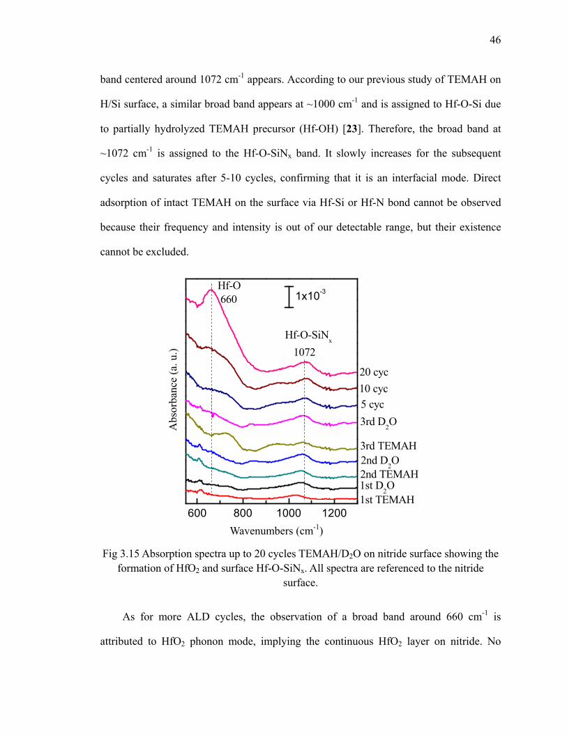
46
band centered around 1072 cm-1 appears. According to our previous study of TEMAH on
H/Si surface, a similar broad band appears at ~1000 cm-1 and is assigned to Hf-O-Si due
to partially hydrolyzed TEMAH precursor (Hf-OH) [23]. Therefore, the broad band at
~1072 cm-1 is assigned to the Hf-O-SiNx band. It slowly increases for the subsequent
cycles and saturates after 5-10 cycles, confirming that it is an interfacial mode. Direct
adsorption of intact TEMAH on the surface via Hf-Si or Hf-N bond cannot be observed
because their frequency and intensity is out of our detectable range, but their existence
cannot be excluded.
600 800 1000 1200
5 cyc10 cyc
1st D2O
1st TEMAH
20 cyc
Hf-O-SiNx
1072
1x10⁻³Hf-O 660
2nd D2O2nd TEMAH
3rd D2O
3rd TEMAH
Fig 3.15 Absorption spectra up to 20 cycles TEMAH/D2O on nitride surface showing the formation of HfO2 and surface Hf-O-SiNx. All spectra are referenced to the nitride
surface.
As for more ALD cycles, the observation of a broad band around 660 cm-1 is
attributed to HfO2 phonon mode, implying the continuous HfO2 layer on nitride. No
Wavenumbers (cm-1)
Abs
orba
nce
(a. u
.)
47
TO/LO SiO2 modes [43] are evidenced, implying that the interfacial SiO2 is minimized
benefiting from the protection of nitride. Since no substantial amount of SiO2 is detected
as well for the HfO2 deposited on H/Si(111) at 100oC, the advantage of SiNx is not as
obvious as the Al2O3 case. However, our further discussion of ozone based ALD of HfO2
on nitride will clearly show the advantage of using nitride to minimize the interfacial
SiO2 in the next chapter.
3.4 Summary
In this chapter, we studied the mechanism of thermal nitridation of H/Si(111) by
NH3 for ALD application, with the aid of in situ FTIR and first principle DFT calculation.
Besides flat H/Si(111) surface, vicinal Si(111) surfaces including monohydride and
dihydride stepped H/Si(111) surfaces are used to study the effect of defects during the
nitridation process. By varying the temperature from 150oC to 600oC at a small
temperature step of 25oC, the surface interaction with NH3 is investigated to conclude the
whole picture of NH3 nitridation.
Flat H/Si(111) surface and monohydride stepped H/Si(111) surface show the same
nitridation behavior due to their structural similarity. Upon 350oC, NH3 dissociates and
replaces the surface Si-H by Si-NH2 species, which is featured by the observation of
scissoring deformation mode of -NH2 and loss of Si-H stretching modes. The nitrogen
atoms start to be inserted into Si-Si network to form SiNx layer around 400oC featured by
the Nx-Si-H mode and SiNx TO/LO modes.
Dihydride stepped H/Si(111) shows a very different nitridation mechanism than the
flat and monohydride cases. Desorption of Si-H begins at 325oC without the observation
of -NH2 scissoring deformation mode. The new mode observed at 775 cm-1 indicates that
48
the thermal nitridation is initiated by forming an H-Si-NH-Si bridging structure at the
step edge and is therefore attributed to Si-H bending mode of the H-Si-NH-Si structure
due to the -NH- bridging process. This process achieves maximum at 375oC. DFT
calculation perfectly confirms our vibrational mode assignments and assumed nitridation
model. Upon 400oC, nitrogen insertion into Si-Si back bond is evidenced by Nx-Si-H
mode and SiNx phonon modes.
With above understandings, HfO2 is deposited on this nitride by TEMAH/D2O. The
precursor structure, properties and ideal reaction mechanism are discussed. Differential
spectra of each precursor dosing captured the ALD ligand exchange by showing the
periodic variation of -OD stretching mode and the HfO2 nucleation is confirmed by its
phonon mode around 660 cm-1.
Bibliography 1. G. W. Trucks, K. Raghavachari, G. S. Higashi and Y. J. Chabal, Mechanism of HF etching of silicon surface: A theoretical understanding of hydrogen passivation, Phys. Rev. Lett. 65 (1990), no. 4, 504. 2. T. Hattori and S. Heusler, Ultraclean surface processing of silicon wafers, Springer (1998). 3. A. Ulman, Formation and structure of self-assembled monolayers, Chem. Rev. 96 (1996), 1533. 4. A. Faucheux, A. C. Gouget-Laemmel, P. A.llongue, C. H. d. Villeneuve, F. Ozanam and J.-N. Chazalviel, Mechanisms of thermal decomposition of organic monolayers grafted on (111) silicon, Langmuir 23 (2007), 1326. 5. J. M. Buriak, Organometallic chemistry on silicon and germanium surfaces, Chem. Rev. 102 (2002), 1271. 6. B. F. Hanyaloglu and E. S. Aydil, Low temperature plasma deposition of silicon nitride from silane and nitrogen plasmas, J. Vac. Sci. Technol. A 16(5) (1998), 2794. 7. J. W. Klaus, A. W. Ott, A. C. Dillon and S. M. George, Atomic layer controlled growth of Si3N4 films using sequential surface reactions, Surface Science 418 (1998), L14. 8. R. T. Brewer, M.-T. Ho, K. Z. Zhang, L. V. Goncharova, D. G. Starodub, T. Gustafsson and Y. J. Chabal, Ammonia pretreatment for high-κ dielectric growth on

49
silicon, Appl. Phys. Lett. 85 (2004), no. 17, 3830. 9. Y. Wang, M. Dai, S. Rivillon, M. T. Ho and Y. J. Chabal, In situ infrared absorption spectroscopy for thin films growth by atomic layer deposition, Proc. SPIE 6325 (2006), 63250G. 10. Y. Wang, M.-T. Ho, L. V. Goncharova, L. S. Wielunski, S. Rivillon-Amy, Y. J. Chabal, T. Gustafsson, N. Moumen and M. Boleslawski, Characterization of ultra-thin hafnium oxide films grown on silicon by atomic layer deposited using tetrakis(ethylmethyl-amino) hafnium and water precursors, Chem. Mater. 19 (2007), 3127. 11. M. M. Frank, Y. Wang, M.-T. Ho, R. T. Brewer, N. Moumen and Y. J. Chabal, Hydrogen barrier layer against silicon oxidation during atomic layer deposition of Al2O3 and HfO2, J. Electrochem. Soc. 154 (2007), no. 2, G44. 12. M. Bjrrkqvist, M. Gothelid and U. O. Karlsson, Nitride formation and dangling-bond passivation on Si(111)-(7 x 7) with NH3, Surface Science 394 (1997), L155-L161. 13. D. R. Bowler and J. H. G. Owen, Molecular interactions and decomposition pathways of NH3 on Si(001), Phys. Rev. B 75 (2007), 155310. 14. J. L. Bischoff, L. Kubler and D. Bolmont, Thermal nitridation of Si(100)-2 × 1 surface by NH3: XPS results, Surface Science 209 (1989), no. 1-2, 115. 15. K. T. Queeney, Y. J. Chabal and K. Raghavachari, Role of interdimer interactions in NH3 dissociation on Si(100), Physical Review Letters 86 (2001), 1046. 16. M. Bjorkquist, M. Gothelid, T. M. Grehk and U. O. Karlsson, NH3 on Si(111)7x7: Dissociation and surface reaction, Physical Review B 57 (1998), no. 4, 2327. 17. M. L. Colaianni, P. j. Chen and J. J. T. Yates, The stepwise dissociation of NH3 on the Si(111)-(7x7) surface: Low-temperature dissociative adsorption and thermal effects, J. Chem. Phys. 96 (1992), no. 10, 7826. 18. J. C. F. Rodríguez-Reyes and A. V. Teplyakov, Cooperative nitrogen insertion processes: Thermal transformation of NH3 on a Si(100) surface, Phys. Rev. B 76 (2007), 075348. 19. Y. I. S. Ishidzuka, T. Takaoka, I. Kusunoki, Nitridation of Si(100) surface with NH3, Applied Surface Science 130-132 (1997), 107. 20. P. Dumas, Y. J. Chabal and G. S. Higashi, Coupling of an adsorbate vibration to a substrate surface phonon: H on Si(1111), Physical Review Letters 65 (1990), 1124. 21. A. C. Dillon, P. Gupta, M. B. Robinson, A. S. Bracher and S. M. George, Ammonia decompostion on silicon surfaces studied using tranmission Fourier transform infrared spectroscopy, J. Vac. Sci. Technol. A 9(4) (1991), 2222. 22. J. Yoshinobu, Physical properties and chemical reactivity of the buckled dimer on Si(100), Progress in Surface Science 77 (2004), 37-70. 23. M.-T. Ho, Y. Wang, R. T. Brewer, L. S. Wielunski and Y. J. Chabal, In situ infrared spectroscopy of hafnium oxide growth on hydrogen-terminated silicon surfaces by atomic layer deposition, Appl. Phys. Lett. 87 (2005), 133103. 24. G. N. Parsons and G. Lucovsky, Silicon-hydrogen bond-stretching vibrations in
50
hydrogenated amorphous silicon-nitrogen alloys, Phys. Rev. B 41 (1990), 1664. 25. D. V. Tsu, G. Lucovsky and B. N. Davidson, Effects of the nearest neighbors and the alloy matrix on SiH stretching vibrations in the amorphous SiOr:H (0<r<2) alloy system, Physical Review B 40 (1989), no. 3, 1795. 26. G. Dupont, H. Caquineau, B. Despax, R. Berjoan and A. Dollet, Structural properties of N-rich a-Si-N:H films with a low electron-trapping rate, J. Phys. D: Appl. Phys 30 (1997), 1064. 27. G. Lucovsky and D. V. Tsu, Plasma enhanced chemical vapor deposition: Differences between direct and remote plasma excitation, J. Vac. Sci. Technol. A 5(4) (1986), 2231. 28. K.-C. Lin and S.-C. Lee, The structural and optical properties of a-SiNx:H prepared by plasma-enhanced chemical-vapor deposition, J. Appl. Phys. 72 (1992), 5474. 29. D. V. Tsu and G. Lucovsky, Silicon nitride and silicon diimide grown by remote plasma enhanced chemical vapor deposition, J. Vac. Sci. Technol. A 4(3) (1986), 480. 30. D. V. Tsu, G. Lucovsky and M. J. Mantini, Local atomic structure in thin films of silicon nitride and silicon diimide produced by remote plasma-enhanced chemical-vapor deposition, Physical Review B 33 (1986), 7069. 31. V. Verlaan, C. H. M., v. d. Werf, W. M. Arnoldbik, H. D. Goldbach and R. E. I. Schropp, Unambiguous determination of Fourier-transform infrared spectroscopy proportionality factors: The case of silicon nitride, Physical Review B 73 (2006), 195333. 32. a. Y. J. C. P. Jakob, Chemical etching of vicinal Si(111): Dependence of the surface structure and the hydrogen termination on the PH of the etching solutions, J. chem. Phys. 95(4) (1991). 33. X. Zhang, Y. J. Chabal, S. B. Christman, E. E. Chaban and E. Garfunkel, Oxidation of H-covered flat and vicinal Si(111)-1x1 surfaces, J. Vac. Sci. Technol. A 19(4) (2000), 1725. 34. Y. J. Chabal, G. S. Higashi, K. Raghavachari and V. A. Burrows, Infrared spectroscopy of Si(111) and Si(100) surfaces after HF treatment: Hydrogen termination and surface morphology, J. Vac. Sci. Technol. A 7(3) (1989), 2104. 35. K. Raghavachari, P. Jakob and Y. J. Chabal, Step relaxation and surface stress at H-terminated vicinal Si(111), Chemical Physics Letters 206 (1993), 156. 36. J. P. Perdew, K. Burke and M. Ernzerhof, Generalized gradient approximation made simple, Phys. Rev. Lett. 77 (1996), 3865. 37. B. Delley, From molecules to solids with the Dmol3 approach, J. Chem. Phys. 113 (2000), 7756. 38. G. D. Wilk, R. M. Wallace and J. M. Anthony, High-k gate dielectrics: Current status and materials properties considerations, Journal of Applied Physics 89 (2001), 5243. 39. High-k and metal gate research, http://www.intel.com/technology/silicon/high-k.htm. 40. S. Yoshihide, P. Seung, C. Hood, B. Lawrence and N. Wesley, Atomic layer deposition of hafnium oxide and hafnium silicate thin films using liquid precursors and
51
ozone, Journal of Vacuum Science & Technology A: Vacuum, Surfaces, and Films 22 (2004), no. 4, 1175-1181. 41. D. M. Hausmann, E. Kim, J. Becker and R. G. Gordon, Atomic layer deposition of hafnium and zirconium oxides using metal amide precursors, Chem. Mater. 14 (2002), 4350. 42. K. Kukli, M. Ritala, T. Sajavaara, J. Keinonen and M. Leskelä, Atomic layer deposition of hafnium dioxide films from hafnium tetrakis(ethylmethylamide) and water, Chemical Vapor Deposition 8 (2002), no. 5, 199. 43. K. T. Queeney, Y. J. Chabal, M. K. Weldon and K. Raghavachari, Silicon oxidation and ultra-thin oxide formation on silicon studied by infrared absorption spectroscopy, Phys. Stat. Sol. (a) 175 (1999), 77.
52
Chapter 4: ALD of Al2O3 and HfO2 with Ozone
H2O is most frequently used oxidant for ALD to deposit metal oxides [1]. However,
most ALD precursors are extremely sensitive to water, and H2O or hydroxyl group (-OH)
tends to be strongly physisorbed on surfaces or in ALD reactor. The trapped water/OH
may release during the metal precursor dosing and hence increase the growth rate making
the deposition more like CVD process. Thus, long purging time is needed to remove the
residue water/OH and hot-wall ALD is necessary to reduce adsorbed water.
Another issue of water based ALD is that the deposited metal oxide film contains
hydroxyl groups [2]. These hydroxyl groups make the film oxygen rich and may oxide
the interface during post-annealing treatment by forming interfacial SiO2, which greatly
minimizes the advantage of using high-κ oxide [3]. In addition, the hydroxyl groups will
degrade the electrical property of high-κ oxide film such as increasing the leakage current.
Therefore, ozone has been used as the oxidant for ALD growth to prevent those
drawbacks caused by water [4, 5, 6, 7, 8]. Studies have shown that ozone based ALD can
deposit high-κ oxide film with improved electrical and structural properties including low
leakage current [9, 10, 11]. Particularly, ozone has several other advantages over water. It
is a strongly-reactive oxidizing agent with high volatility. The concentration and flow of
ozone can be easily controlled compared with water vapor. In addition, it is not sticky and
can be easily purged away. The decomposed product of ozone is oxygen which is
harmless. So it is becoming a promising alternative ALD oxidant. However, the carbon
contamination and complicated reaction mechanism are common issues for ozone.
Despite its importance, the mechanistic study of ozone based ALD is rare and the
mechanism is not well understood. So, this chapter will discuss the ozone based ALD
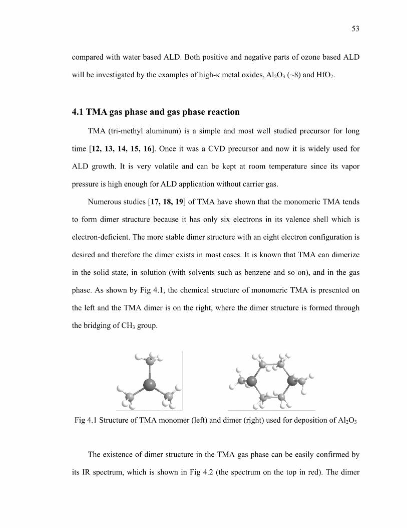
53
compared with water based ALD. Both positive and negative parts of ozone based ALD
will be investigated by the examples of high-κ metal oxides, Al2O3 (~8) and HfO2.
4.1 TMA gas phase and gas phase reaction
TMA (tri-methyl aluminum) is a simple and most well studied precursor for long
time [12, 13, 14, 15, 16]. Once it was a CVD precursor and now it is widely used for
ALD growth. It is very volatile and can be kept at room temperature since its vapor
pressure is high enough for ALD application without carrier gas.
Numerous studies [17, 18, 19] of TMA have shown that the monomeric TMA tends
to form dimer structure because it has only six electrons in its valence shell which is
electron-deficient. The more stable dimer structure with an eight electron configuration is
desired and therefore the dimer exists in most cases. It is known that TMA can dimerize
in the solid state, in solution (with solvents such as benzene and so on), and in the gas
phase. As shown by Fig 4.1, the chemical structure of monomeric TMA is presented on
the left and the TMA dimer is on the right, where the dimer structure is formed through
the bridging of CH3 group.
Fig 4.1 Structure of TMA monomer (left) and dimer (right) used for deposition of Al2O3
The existence of dimer structure in the TMA gas phase can be easily confirmed by
its IR spectrum, which is shown in Fig 4.2 (the spectrum on the top in red). The dimer

54
and monomer can be identified by the band shift of -CH3 due to -CH3 bridging. For
example, the stretching modes of -CH3 at 2800-3000 cm-1 are split into the bridged -CH3
modes and terminal -CH3 modes, along with many other bridged modes and terminal
modes. The detailed band assignments are shown in table 4.1. Note that in spite of some
debates for the assignments [20, 21, 22, 23, 24], there is no doubt that large extent of
TMA dimer exists inside the gas phase. The gas phase spectrum is identical to that in
other studies and trivial amount of CH4 is observed, implying little hydrolysis or
decomposition of TMA. Thus, it can be concluded that the TMA is quite pure before
further ALD reaction.
1000 2000 3000 4000
νt as(C
H3)
ρb (CH
3)
D2O
ν(CH
4 )
δ(CH
4 )νb as
(CH
3)
ρt(CH3)νt
s(Al-C)
ρb (CH
3)
νb s(Al-C
)
δb (CH
3)δt (CH
3)
νt s(CH
3)
ν(CD
4 )
2x10⁻¹
TMA
Fig 4.2 The TMA gas phase spectrum and the spectrum after reaction with D2O. The spectrum on the top in red shows the TMA gas phase (referenced to vacuum) and the
spectrum at the bottom in black is after D2O exposure (referenced to TMA). The superscript ‘b’ denotes the ‘bridged’ and ‘t’ denotes ‘terminal’. The TMA ligand features
disappear after D2O.
Using TMA and water to deposit Al2O3 has been extensively studied. But direct gas
phase reaction study is rare. Here, after introducing the gas phase TMA into the ALD
reactor and taking the spectrum, D2O is introduced in to study the reaction byproducts
and then the detailed reaction can be concluded. As in Fig 4.2, the spectrum at the bottom
Wavenumbers (cm-1)
Abs
orba
nce
(a. u
.)
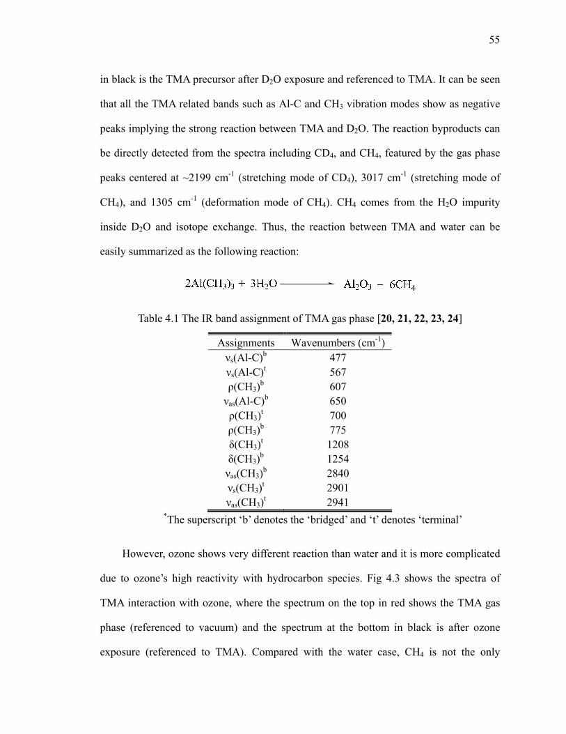
55
in black is the TMA precursor after D2O exposure and referenced to TMA. It can be seen
that all the TMA related bands such as Al-C and CH3 vibration modes show as negative
peaks implying the strong reaction between TMA and D2O. The reaction byproducts can
be directly detected from the spectra including CD4, and CH4, featured by the gas phase
peaks centered at ~2199 cm-1 (stretching mode of CD4), 3017 cm-1 (stretching mode of
CH4), and 1305 cm-1 (deformation mode of CH4). CH4 comes from the H2O impurity
inside D2O and isotope exchange. Thus, the reaction between TMA and water can be
easily summarized as the following reaction:
Table 4.1 The IR band assignment of TMA gas phase [20, 21, 22, 23, 24]
Assignments Wavenumbers (cm-1)νs(Al-C)b 477 νs(Al-C)t 567 ρ(CH3)b 607 νas(Al-C)b 650 ρ(CH3)t 700 ρ(CH3)b 775 δ(CH3)t 1208 δ(CH3)b 1254 νas(CH3)b 2840 νs(CH3)t 2901 νas(CH3)t 2941
*The superscript ‘b’ denotes the ‘bridged’ and ‘t’ denotes ‘terminal’
However, ozone shows very different reaction than water and it is more complicated
due to ozone’s high reactivity with hydrocarbon species. Fig 4.3 shows the spectra of
TMA interaction with ozone, where the spectrum on the top in red shows the TMA gas
phase (referenced to vacuum) and the spectrum at the bottom in black is after ozone
exposure (referenced to TMA). Compared with the water case, CH4 is not the only
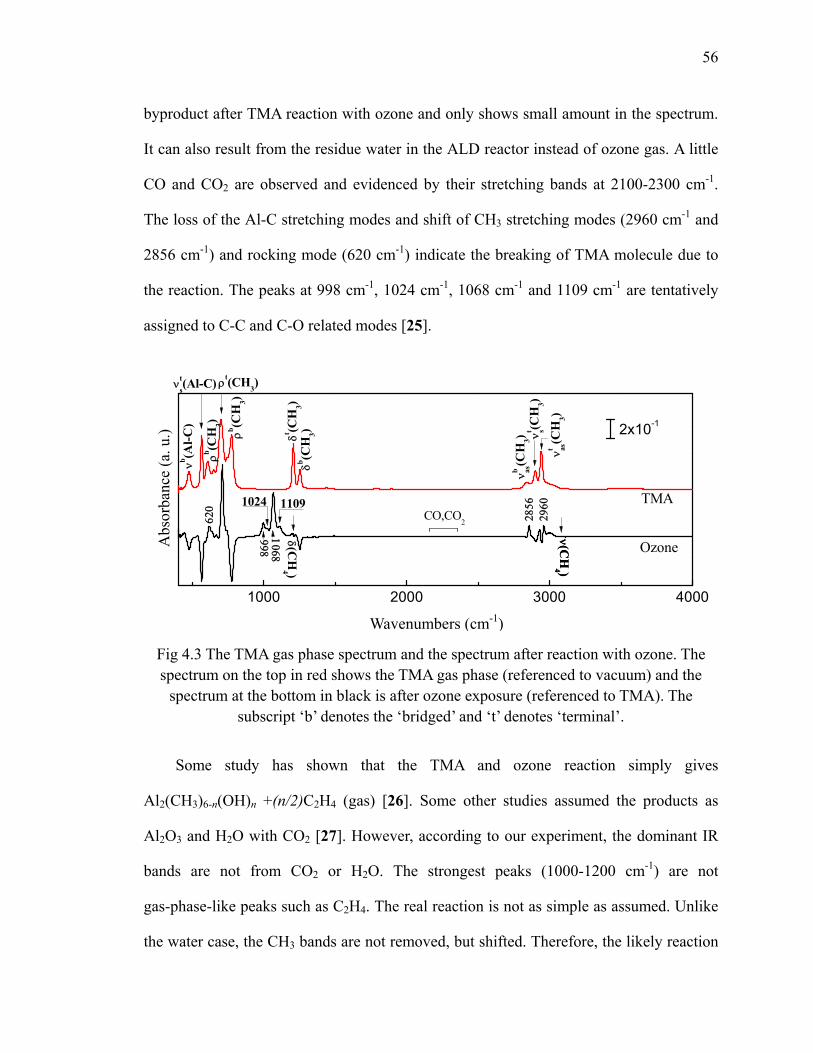
56
byproduct after TMA reaction with ozone and only shows small amount in the spectrum.
It can also result from the residue water in the ALD reactor instead of ozone gas. A little
CO and CO2 are observed and evidenced by their stretching bands at 2100-2300 cm-1.
The loss of the Al-C stretching modes and shift of CH3 stretching modes (2960 cm-1 and
2856 cm-1) and rocking mode (620 cm-1) indicate the breaking of TMA molecule due to
the reaction. The peaks at 998 cm-1, 1024 cm-1, 1068 cm-1 and 1109 cm-1 are tentatively
assigned to C-C and C-O related modes [25].
1000 2000 3000 4000
CO,CO2620 1024
998
2856
ν(CH
4 )
2960
Ozoneνt as
(CH
3)
2x10⁻¹
νb (Al-C
)
ρb (CH
3)
δt (CH
3)δb (C
H3)
νb as(C
H3) νt s(C
H3)
TMA
ρt(CH3)
ρb (CH
3)
νts(Al-C)
ν(CH
4 )
δ(CH
4 )1068
1109
Fig 4.3 The TMA gas phase spectrum and the spectrum after reaction with ozone. The spectrum on the top in red shows the TMA gas phase (referenced to vacuum) and the
spectrum at the bottom in black is after ozone exposure (referenced to TMA). The subscript ‘b’ denotes the ‘bridged’ and ‘t’ denotes ‘terminal’.
Some study has shown that the TMA and ozone reaction simply gives
Al2(CH3)6-n(OH)n +(n/2)C2H4 (gas) [26]. Some other studies assumed the products as
Al2O3 and H2O with CO2 [27]. However, according to our experiment, the dominant IR
bands are not from CO2 or H2O. The strongest peaks (1000-1200 cm-1) are not
gas-phase-like peaks such as C2H4. The real reaction is not as simple as assumed. Unlike
the water case, the CH3 bands are not removed, but shifted. Therefore, the likely reaction
Wavenumbers (cm-1)
Abs
orba
nce
(a. u
.)
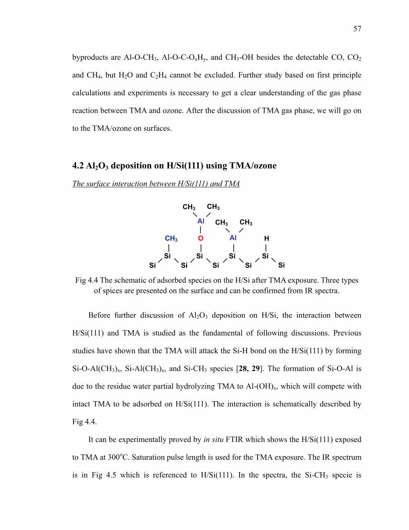
57
byproducts are Al-O-CH3, Al-O-C-OxHy, and CH3-OH besides the detectable CO, CO2
and CH4, but H2O and C2H4 cannot be excluded. Further study based on first principle
calculations and experiments is necessary to get a clear understanding of the gas phase
reaction between TMA and ozone. After the discussion of TMA gas phase, we will go on
to the TMA/ozone on surfaces.
4.2 Al2O3 deposition on H/Si(111) using TMA/ozone
The surface interaction between H/Si(111) and TMA
Fig 4.4 The schematic of adsorbed species on the H/Si after TMA exposure. Three types
of spices are presented on the surface and can be confirmed from IR spectra.
Before further discussion of Al2O3 deposition on H/Si, the interaction between
H/Si(111) and TMA is studied as the fundamental of following discussions. Previous
studies have shown that the TMA will attack the Si-H bond on the H/Si(111) by forming
Si-O-Al(CH3)x, Si-Al(CH3)x, and Si-CH3 species [28, 29]. The formation of Si-O-Al is
due to the residue water partial hydrolyzing TMA to Al-(OH)x, which will compete with
intact TMA to be adsorbed on H/Si(111). The interaction is schematically described by
Fig 4.4.
It can be experimentally proved by in situ FTIR which shows the H/Si(111) exposed
to TMA at 300oC. Saturation pulse length is used for the TMA exposure. The IR spectrum
is in Fig 4.5 which is referenced to H/Si(111). In the spectra, the Si-CH3 specie is
Al CH3
Si Si
CH3
Si Si
Si
O
Si Si
CH3 CH3
Si Si
H Al
CH3

58
confirmed by CH3 rocking mode at 770 cm-1 and deformation mode 1248 cm-1, the
Si-O-Al(CH3)x specie is confirmed by the broad peak at 984 cm-1 which is Si-O mode
shifted by Al atom, and the Al-CH3 specie is confirmed by the CH3 deformation mode at
1217 cm-1. The Al-CH3 directly attaching Si via Si-Al bond cannot be observed in the
spectrum, because it is out of our detection ability. However, the band analysis of Al-CH3
deformation mode by previous study shows the existence of direct bond of Si-Al [28],
where the methyl deformation mode observed at 1217 cm-1 with a shoulder at 1206 cm-1
is a useful indicator of Si-Al bonding environment. According to our single unit cell
cluster DFT calculation, the -CH3 umbrella deformation mode of Si-O-Al-CH3 is ∼6 cm-1
higher than that of Si-Al-CH3. This suggests that Al-CH3 of TMA is attached to Si atoms
either directly or through O atoms.
900 1200 2100 2400 2700 3000
1st TMA on H/Si(111)
ν(CH3)
ν(Si-H)δ(Si-CH3)
δ(Al-CH3)Si-O-Al
1x10⁻⁴ρ(Si-CH3)
Fig 4.5 IR absorption spectrum of H/Si(111) exposed by TMA at 300 oC which is
referenced to H/Si(111) at incident angle ~74o. The inset shows the initial H/Si(111) (spectrum at the bottom in black ) and the surface after TMA exposure (spectrum on top
and in red) which are all referenced to SiO2.
The variation of Si-H at 2083 cm-1 indicates the adsorption of TMA on H/Si(111) by
replacing Si-H. The coverage can be deduced by the loss of Si-H. As shown by the inset
of Fig 4.5 which is referenced to SiO2 surface, the initial Si-H (bottom spectrum in black)
at 2083 cm-1 decreases and red shifts to 2050 cm-1 due to decoupling of Si-H by the
1950 2000 2050 2100 2150
After TMA
5x10⁻⁴
H/Si(111)
Wavenumbers (cm-1)
Abs
orba
nce
(a. u
.)
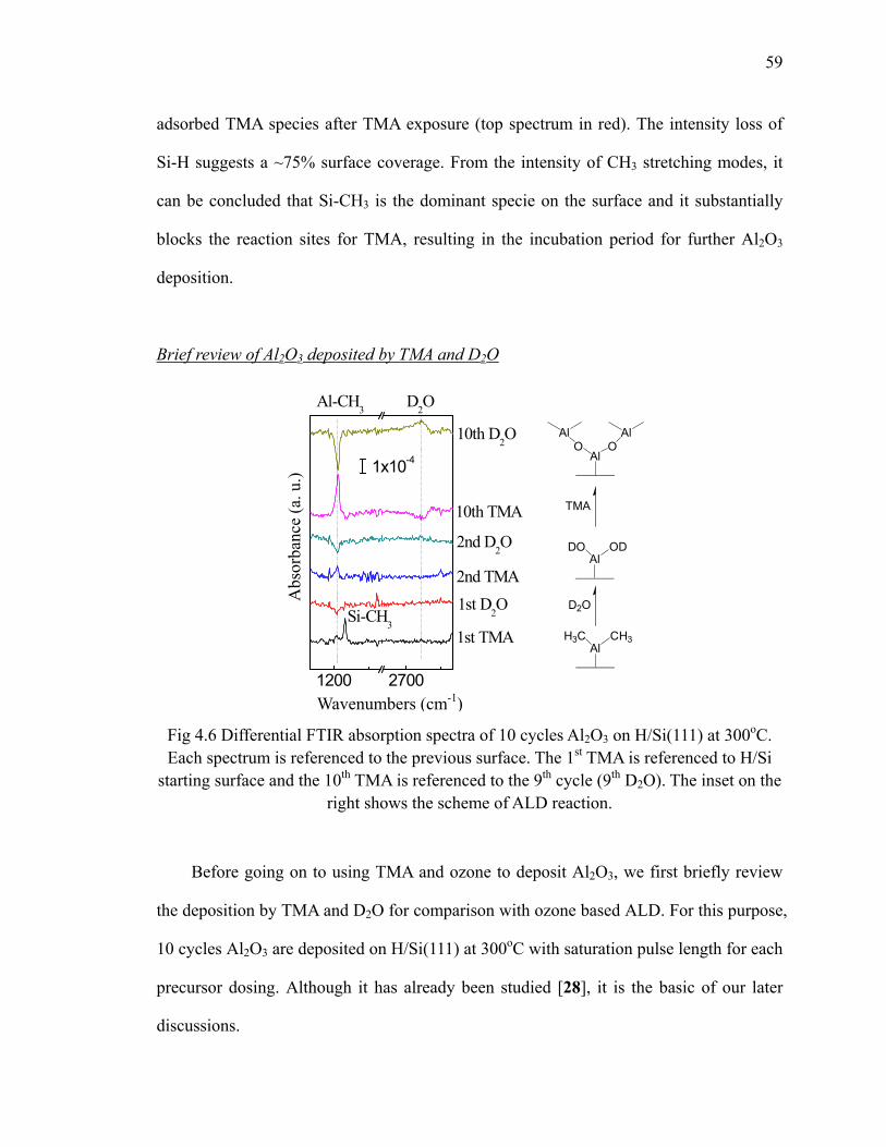
59
adsorbed TMA species after TMA exposure (top spectrum in red). The intensity loss of
Si-H suggests a ~75% surface coverage. From the intensity of CH3 stretching modes, it
can be concluded that Si-CH3 is the dominant specie on the surface and it substantially
blocks the reaction sites for TMA, resulting in the incubation period for further Al2O3
deposition.
Brief review of Al2O3 deposited by TMA and D2O
Fig 4.6 Differential FTIR absorption spectra of 10 cycles Al2O3 on H/Si(111) at 300oC. Each spectrum is referenced to the previous surface. The 1st TMA is referenced to H/Si
starting surface and the 10th TMA is referenced to the 9th cycle (9th D2O). The inset on the right shows the scheme of ALD reaction.
Before going on to using TMA and ozone to deposit Al2O3, we first briefly review
the deposition by TMA and D2O for comparison with ozone based ALD. For this purpose,
10 cycles Al2O3 are deposited on H/Si(111) at 300oC with saturation pulse length for each
precursor dosing. Although it has already been studied [28], it is the basic of our later
discussions.
1200 2700
Si-CH3
2nd D2O
1st D2O2nd TMA
1x10⁻⁴
1st TMA
10th D2O
10th TMA
Al-CH3 D2O
AlH3C CH3
D2O
AlDO OD
Al
TMA
O OAl Al
Wavenumbers (cm-1)
Abs
orba
nce
(a. u
.)

60
Fig 4.6 shows the differential spectra of 10 cycles Al2O3, where each spectrum is
referenced to the previous surface and the bottom is referenced to H/Si(111). The 1st
TMA on H/Si has been discussed in detail in the previous section. The subsequent D2O
pulse removes the -CH3 ligands on Al as expected, featured by the negative peak at 1217
cm-1 (the deformation mode of Al-CH3) and putting -OD groups onto Al. The next TMA
pulse replaces the -OD groups and is attached to the Al via O-Al bond, evidenced by the
positive peak at 1217 cm-1 (the deformation mode of Al-CH3). This process repeats and
Al2O3 is deposited monolayer by monolayer. The reaction scheme is described in the
inset of Fig 4.6 on the right side. Note that the 10th cycle shows stronger intensity for
Al-CH3 variation at 1217 cm-1 and for the broad -OD stretching band variation at 2760
cm-1, as the ALD ligand exchange phenomena. It confirms the ALD scheme and indicates
the initial incubation period in the Al2O3 ALD growth.
Fig 4.7 Absorption spectra of 10 cycles Al2O3 on H/Si(111) at 300oC. All spectra are
referenced to the H/Si(111) surface. SiOx, Al2O3, carbon impurity and trapped water are observed in the spectra.
The spectra in Fig 4.7 are referenced to initial H/Si which are used to examine the
800 1000 1200 2100 2800 3000
5x10⁻⁴
δ(Si-H)
Si-O
Al-Oρ(CH3)
ν(CH3)ν(D2O)δ(Si-CH3)
1x10⁻⁴
2nd D2O
1st D2O2nd TMA
1st TMA
10 cycles
9 cycles
Wavenumbers (cm-1)
Abs
orba
nce
(a. u
.)
61
chemical species in the film. The broad band centered at 906 cm-1 keeps growing with
more cycles. It is assigned to the Al-O phonon mode, confirming the formation of
continuous Al2O3 film with nearly complete Si-H loss. The shoulder appears at
1000-1200 cm-1 is due to the interfacial Si-O, and the amount is minimal because no
individual TO/LO modes are observed. The -OD stretching band at 2760 cm-1 indicates
the existence of trapped D2O/OD substance inside the film. The -CH3 modes at 770 cm-1
(Si-CH3 rocking), 1248 cm-1 (Si-CH3 deformation), 1217 cm-1 (Al-CH3 deformation), and
2800-3000 cm-1 (CH3 stretching), suggest the detectable amount of hydrocarbon
impurities in the film.
With above knowledge, we will discuss ozone based ALD in the following sections.
First we will investigate the ozone ALD growth with excessive ozone pulse length, and
then the growth with shorter ozone pulse length will be discussed to show the
improvement in the film quality.
Al2O3 deposited by TMA and ozone(I)-long ozone pulse
The deposition with long ozone pulse length will be discussed first. The ALD of
TMA+ozone on H/Si(111) is performed at 300oC for 20 cycles. Saturation pulse length
for TMA and excessive pulse length for ozone are used, where the ozone exposure
amount is 200sccm for 2s. The differentia spectra are shown in Fig 4.8. The H/Si surface
after first TMA dosing has been discussed in the previous section. The methyl
deformation mode of Al-CH3 at 1217 cm-1 and loss of Si-H at 2083 cm-1 indicate
adsorbed TMA on the surface. The Si-CH3 rocking mode (770 cm-1) and deformation
mode (1248 cm-1) are observed as well as the Al-O-Si band at 984 cm-1.
After the 1st ozone exposure, the surface is oxidized immediately shown by SiO2
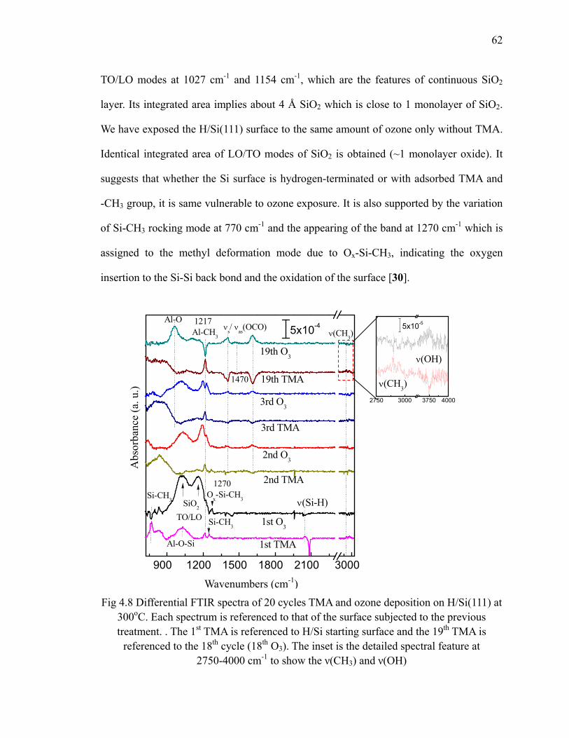
62
TO/LO modes at 1027 cm-1 and 1154 cm-1, which are the features of continuous SiO2
layer. Its integrated area implies about 4 Å SiO2 which is close to 1 monolayer of SiO2.
We have exposed the H/Si(111) surface to the same amount of ozone only without TMA.
Identical integrated area of LO/TO modes of SiO2 is obtained (~1 monolayer oxide). It
suggests that whether the Si surface is hydrogen-terminated or with adsorbed TMA and
-CH3 group, it is same vulnerable to ozone exposure. It is also supported by the variation
of Si-CH3 rocking mode at 770 cm-1 and the appearing of the band at 1270 cm-1 which is
assigned to the methyl deformation mode due to Ox-Si-CH3, indicating the oxygen
insertion to the Si-Si back bond and the oxidation of the surface [30].
Fig 4.8 Differential FTIR spectra of 20 cycles TMA and ozone deposition on H/Si(111) at 300oC. Each spectrum is referenced to that of the surface subjected to the previous treatment. . The 1st TMA is referenced to H/Si starting surface and the 19th TMA is
referenced to the 18th cycle (18th O3). The inset is the detailed spectral feature at 2750-4000 cm-1 to show the ν(CH3) and ν(OH)
2750 3000 3750 4000
ν(OH)
5x10⁻⁵
ν(CH3)
900 1200 1500 1800 2100 3000
1470
Al-O
ν(Si-H)
νs/ νas(OCO) ν(CH3)
1217 Al-CH3
Si-CH3
Si-CH3
1270 Ox-Si-CH3
Al-O-Si
5x10⁻⁴
SiO2
TO/LO
2nd O3
1st O3
2nd TMA
1st TMA
3rd O3
3rd TMA
19th O3
19th TMA
Wavenumbers (cm-1)
Abs
orba
nce
(a. u
.)
63
The further loss of Si-H confirms the attacking of ozone to the Si surface at later
cycles. This oxide phonon band is disrupted after each TMA pulse because of the
chemical bonding between the surface Si-O-Si matrix and TMA. The subsequent TMA
and ozone pulses show the periodic gain and loss of Al-CH3 at 1217 cm-1 and -CH3
stretches at 2800-3000 cm-1, suggesting the ALD ligand exchange and the continuous
growth of Al2O3. That is, after TMA, the Al-CH3 is attached to the surface and after
ozone, the -CH3 is attacked. But the actual reaction mechanism is not so simple.
From the second cycle, several new bands have been observed accompanied by the
variation of Al-CH3 deformation mode. The weak band at 1470 cm-1 is assigned to
Al-O-CH3 methyl deformation mode indicating the insertion of oxygen into Al-C bond
after ozone exposure. More important, the bands at 1400 cm-1 and 1610 cm-1 are assigned
to the formate (OCHO-) species on the surface [31, 32]. The 1600 cm-1 band is the
asymmetric stretching mode while the 1400 cm-1 band can be deconvoluted to three
bands at 1405, 1385 and 1360 cm-1. These bands are attributed to OCO deformation, CH
in-plane bending and OCO symmetric stretching modes of the formate species,
respectively [31]. At 300oC, the formate species can decompose to gas-phase CO or CO2,
producing OH groups on the surface [33]. These hydroxyl groups out of the formate
decomposition are most likely the origin of the -OH stretching band at 3750 cm-1 after
each ozone pulse as shown by the inset of Fig 4.8.
To support our band assignments and rule out other possible surface species,
periodic and cluster based first principle calculations are carried out (done by Dr. Mathew
Halls). The calculations using the density functional theory (DFT) code DMol3 are
carried out [34], using all-electron calculations with the gradient corrected PBE [35]
functional along with a double numeric polarized basis set (DNP). The vibrational modes
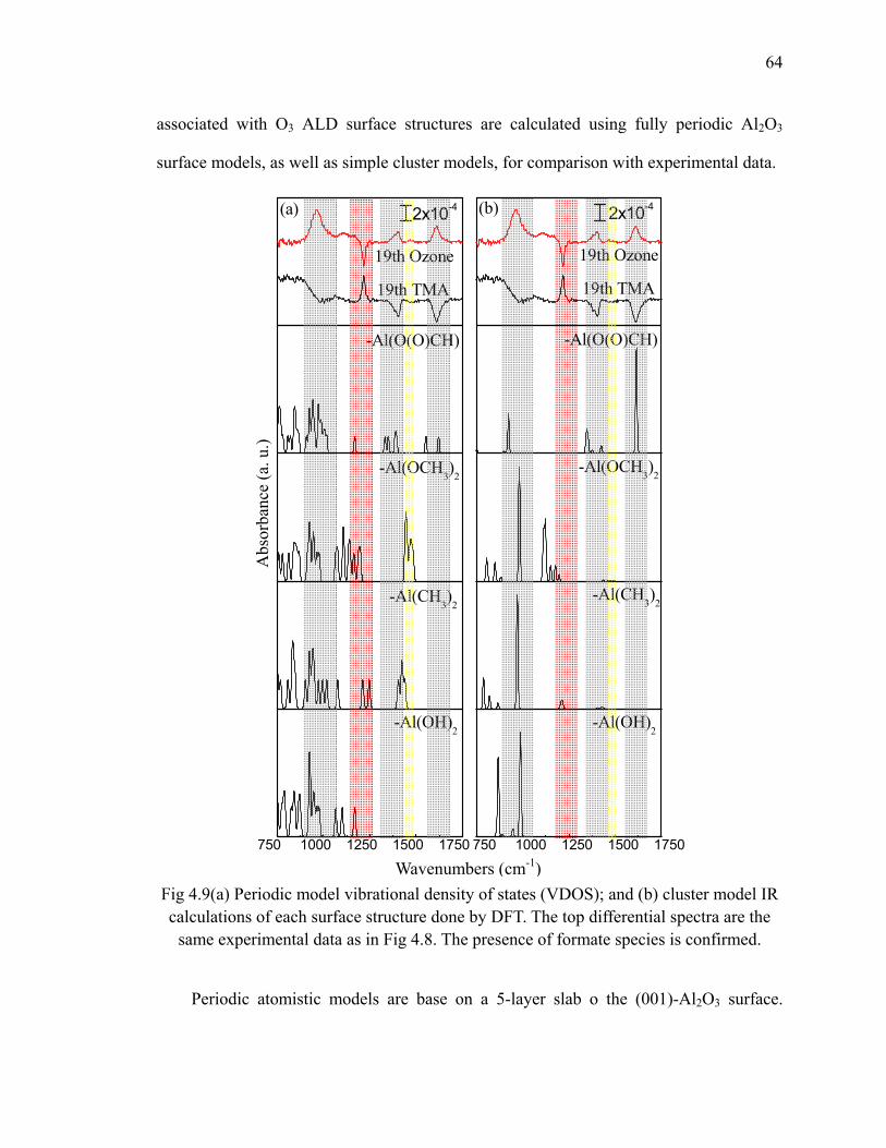
64
associated with O3 ALD surface structures are calculated using fully periodic Al2O3
surface models, as well as simple cluster models, for comparison with experimental data.
(b)(a)
19th Ozone
19th TMA
2x10⁻⁴ 2x10⁻⁴
19th Ozone
19th TMA
-Al(CH3)2-Al(CH3)2
-Al(OCH3)2-Al(OCH3)2
-Al(O(O)CH)-Al(O(O)CH)
-Al(OH)2-Al(OH)2
750 1000 1250 1500 1750
750 1000 1250 1500 1750
Fig 4.9(a) Periodic model vibrational density of states (VDOS); and (b) cluster model IR calculations of each surface structure done by DFT. The top differential spectra are the
same experimental data as in Fig 4.8. The presence of formate species is confirmed.
Periodic atomistic models are base on a 5-layer slab o the (001)-Al2O3 surface.
Wavenumbers (cm-1)
Abs
orba
nce
(a. u
.)
65
Calculations are carried out for the -Al(CH3)2, -Al(OCH3)2, -Al(OH)2, and -Al(OOCH)
species using 2×1 and 2×2 supercells, respectively, with a 20 Å vacuum slab. A
Monkhorst-Pack k-point mesh with a spacing of 0.04 Å-1 was used to sample the
Brillouin zone. For the cluster models, cluster stoichiometries of Al2O3H2-(CH3)2,
Al2O3H2-(OCH3)2, Al2O3H2-(OH)2 and Al2O3-(OOCH)2 were used.
Fig 4.9(a) shows the calculated vibrational density of states from periodic Al2O3
surface models and Fig 4.9(b) shows the computed vibrational frequencies with
corresponding intensities from cluster adsorbate models, along with the experimental
spectra (top panel) for comparison. The shaded vertical areas represent characteristic
wavenumber regions are included to facilitate comparison between the experiment and
theory. The surface species considered in the calculations include methyl -Al(CH3)2 (red
bar), methoxy -Al(OCH3)2 (yellow bar), formate -Al(OOCH) (gray bars) and hydroxyl
-Al(OH)2. Comparison of the observed IR spectra with the computed spectra for both the
periodic (Fig 4.9(a)) and cluster models (Fig 4.9(b)) supports our assignments. The
predicted frequencies for the -Al(CH3)2 umbrella modes at 1211-1240 cm-1 can be
compared with the observed frequency at 1217 cm-1. The computed frequencies of
1473-1483 cm-1 for the methoxy species correspond to the -Al(OCH3)2 deformation seen
in the IR at 1470 cm-1.
As shown in Figure 4.9, only the symmetric and asymmetric OCO stretching
vibrations are calculated to be at 1350 and 1622 cm-1, respectively, in good agreement
with experimental values (1360 cm-1 and 1610 cm-1). In general, there are two different
formate-aluminum bidentate geometries: a chelating structure, in which each formate
binds to a single Al center, and a bridging structure, where a formate bridges between two
Al centers. The computed νas(OCO) and νs(OCO) modes are comparable for these two
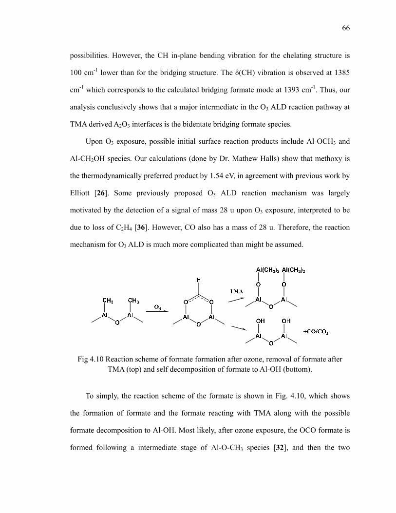
66
possibilities. However, the CH in-plane bending vibration for the chelating structure is
100 cm-1 lower than for the bridging structure. The δ(CH) vibration is observed at 1385
cm-1 which corresponds to the calculated bridging formate mode at 1393 cm-1. Thus, our
analysis conclusively shows that a major intermediate in the O3 ALD reaction pathway at
TMA derived A2O3 interfaces is the bidentate bridging formate species.
Upon O3 exposure, possible initial surface reaction products include Al-OCH3 and
Al-CH2OH species. Our calculations (done by Dr. Mathew Halls) show that methoxy is
the thermodynamically preferred product by 1.54 eV, in agreement with previous work by
Elliott [26]. Some previously proposed O3 ALD reaction mechanism was largely
motivated by the detection of a signal of mass 28 u upon O3 exposure, interpreted to be
due to loss of C2H4 [36]. However, CO also has a mass of 28 u. Therefore, the reaction
mechanism for O3 ALD is much more complicated than might be assumed.
Fig 4.10 Reaction scheme of formate formation after ozone, removal of formate after
TMA (top) and self decomposition of formate to Al-OH (bottom).
To simply, the reaction scheme of the formate is shown in Fig. 4.10, which shows
the formation of formate and the formate reacting with TMA along with the possible
formate decomposition to Al-OH. Most likely, after ozone exposure, the OCO formate is
formed following a intermediate stage of Al-O-CH3 species [32], and then the two
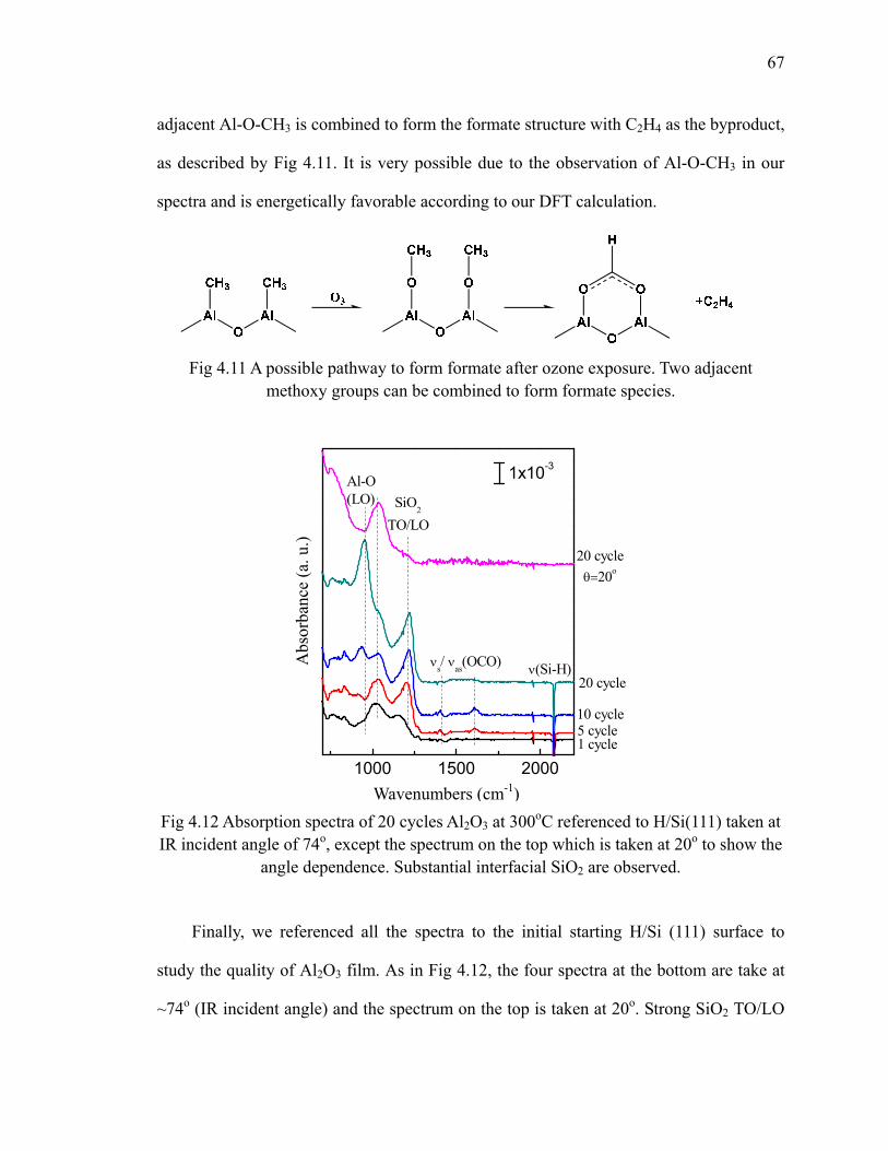
67
adjacent Al-O-CH3 is combined to form the formate structure with C2H4 as the byproduct,
as described by Fig 4.11. It is very possible due to the observation of Al-O-CH3 in our
spectra and is energetically favorable according to our DFT calculation.
Fig 4.11 A possible pathway to form formate after ozone exposure. Two adjacent
methoxy groups can be combined to form formate species.
1000 1500 2000
20 cycle θ=20o
20 cycle
10 cycle5 cycle1 cycle
Al-O (LO)
1x10⁻³
νs/ νas(OCO) ν(Si-H)
SiO2
TO/LO
Fig 4.12 Absorption spectra of 20 cycles Al2O3 at 300oC referenced to H/Si(111) taken at IR incident angle of 74o, except the spectrum on the top which is taken at 20o to show the
angle dependence. Substantial interfacial SiO2 are observed.
Finally, we referenced all the spectra to the initial starting H/Si (111) surface to
study the quality of Al2O3 film. As in Fig 4.12, the four spectra at the bottom are take at
~74o (IR incident angle) and the spectrum on the top is taken at 20o. Strong SiO2 TO/LO
Wavenumbers (cm-1)
Abs
orba
nce
(a. u
.)
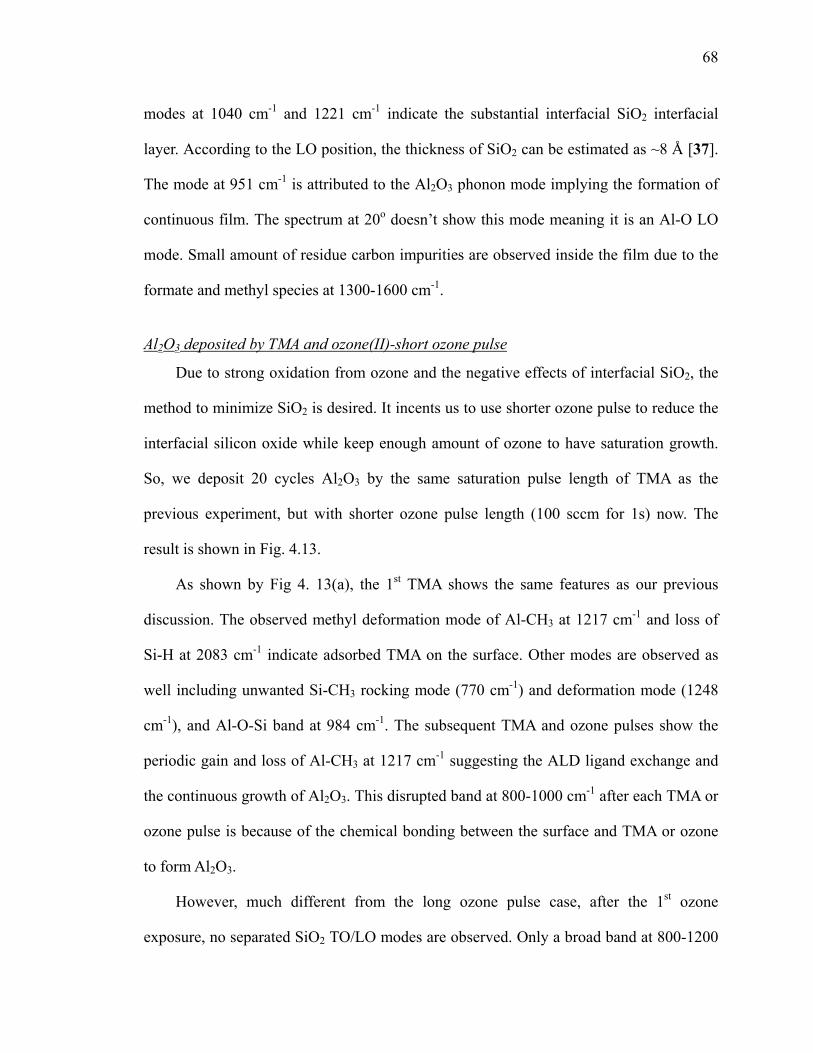
68
modes at 1040 cm-1 and 1221 cm-1 indicate the substantial interfacial SiO2 interfacial
layer. According to the LO position, the thickness of SiO2 can be estimated as ~8 Å [37].
The mode at 951 cm-1 is attributed to the Al2O3 phonon mode implying the formation of
continuous film. The spectrum at 20o doesn’t show this mode meaning it is an Al-O LO
mode. Small amount of residue carbon impurities are observed inside the film due to the
formate and methyl species at 1300-1600 cm-1.
Al2O3 deposited by TMA and ozone(II)-short ozone pulse
Due to strong oxidation from ozone and the negative effects of interfacial SiO2, the
method to minimize SiO2 is desired. It incents us to use shorter ozone pulse to reduce the
interfacial silicon oxide while keep enough amount of ozone to have saturation growth.
So, we deposit 20 cycles Al2O3 by the same saturation pulse length of TMA as the
previous experiment, but with shorter ozone pulse length (100 sccm for 1s) now. The
result is shown in Fig. 4.13.
As shown by Fig 4. 13(a), the 1st TMA shows the same features as our previous
discussion. The observed methyl deformation mode of Al-CH3 at 1217 cm-1 and loss of
Si-H at 2083 cm-1 indicate adsorbed TMA on the surface. Other modes are observed as
well including unwanted Si-CH3 rocking mode (770 cm-1) and deformation mode (1248
cm-1), and Al-O-Si band at 984 cm-1. The subsequent TMA and ozone pulses show the
periodic gain and loss of Al-CH3 at 1217 cm-1 suggesting the ALD ligand exchange and
the continuous growth of Al2O3. This disrupted band at 800-1000 cm-1 after each TMA or
ozone pulse is because of the chemical bonding between the surface and TMA or ozone
to form Al2O3.
However, much different from the long ozone pulse case, after the 1st ozone
exposure, no separated SiO2 TO/LO modes are observed. Only a broad band at 800-1200
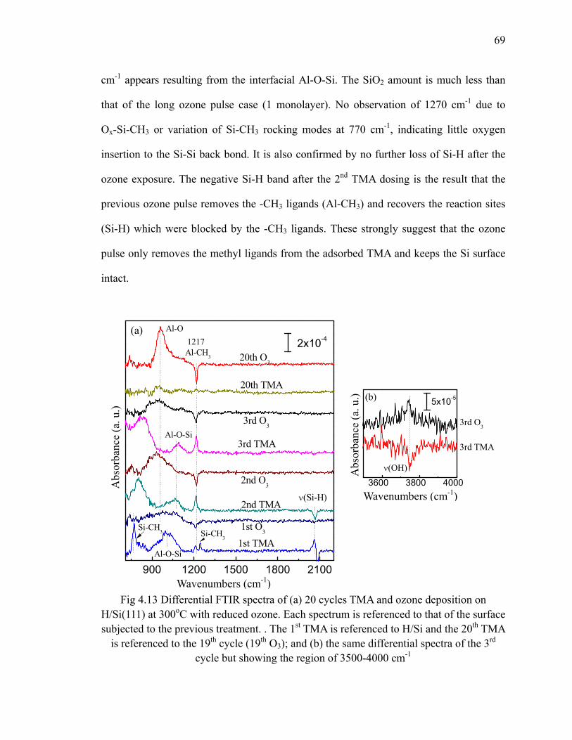
69
cm-1 appears resulting from the interfacial Al-O-Si. The SiO2 amount is much less than
that of the long ozone pulse case (1 monolayer). No observation of 1270 cm-1 due to
Ox-Si-CH3 or variation of Si-CH3 rocking modes at 770 cm-1, indicating little oxygen
insertion to the Si-Si back bond. It is also confirmed by no further loss of Si-H after the
ozone exposure. The negative Si-H band after the 2nd TMA dosing is the result that the
previous ozone pulse removes the -CH3 ligands (Al-CH3) and recovers the reaction sites
(Si-H) which were blocked by the -CH3 ligands. These strongly suggest that the ozone
pulse only removes the methyl ligands from the adsorbed TMA and keeps the Si surface
intact.
900 1200 1500 1800 2100
(a)
Al-O-Si
Si-CH3
2x10⁻⁴
20th O3
20th TMA
3rd O3
3rd TMA
2nd O3
2nd TMA
1st O3
1st TMA
ν(Si-H)
1217 Al-CH3
Al-O
Si-CH3
Al-O-Si
Fig 4.13 Differential FTIR spectra of (a) 20 cycles TMA and ozone deposition on
H/Si(111) at 300oC with reduced ozone. Each spectrum is referenced to that of the surface subjected to the previous treatment. . The 1st TMA is referenced to H/Si and the 20th TMA
is referenced to the 19th cycle (19th O3); and (b) the same differential spectra of the 3rd cycle but showing the region of 3500-4000 cm-1
3600 3800 4000
3rd O3
3rd TMA
5x10⁻⁵
ν(OH)
(b)
Wavenumbers (cm-1)
Abs
orba
nce
(a. u
.)
Wavenumbers (cm-1)
Abs
orba
nce
(a. u
.)
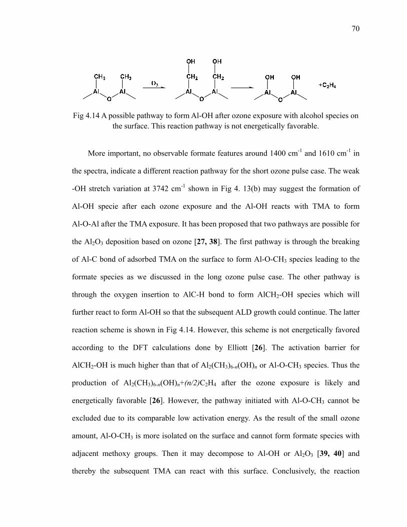
70
Fig 4.14 A possible pathway to form Al-OH after ozone exposure with alcohol species on
the surface. This reaction pathway is not energetically favorable.
More important, no observable formate features around 1400 cm-1 and 1610 cm-1 in
the spectra, indicate a different reaction pathway for the short ozone pulse case. The weak
-OH stretch variation at 3742 cm-1 shown in Fig 4. 13(b) may suggest the formation of
Al-OH specie after each ozone exposure and the Al-OH reacts with TMA to form
Al-O-Al after the TMA exposure. It has been proposed that two pathways are possible for
the Al2O3 deposition based on ozone [27, 38]. The first pathway is through the breaking
of Al-C bond of adsorbed TMA on the surface to form Al-O-CH3 species leading to the
formate species as we discussed in the long ozone pulse case. The other pathway is
through the oxygen insertion to AlC-H bond to form AlCH2-OH species which will
further react to form Al-OH so that the subsequent ALD growth could continue. The latter
reaction scheme is shown in Fig 4.14. However, this scheme is not energetically favored
according to the DFT calculations done by Elliott [26]. The activation barrier for
AlCH2-OH is much higher than that of Al2(CH3)6-n(OH)n or Al-O-CH3 species. Thus the
production of Al2(CH3)6-n(OH)n+(n/2)C2H4 after the ozone exposure is likely and
energetically favorable [26]. However, the pathway initiated with Al-O-CH3 cannot be
excluded due to its comparable low activation energy. As the result of the small ozone
amount, Al-O-CH3 is more isolated on the surface and cannot form formate species with
adjacent methoxy groups. Then it may decompose to Al-OH or Al2O3 [39, 40] and
thereby the subsequent TMA can react with this surface. Conclusively, the reaction
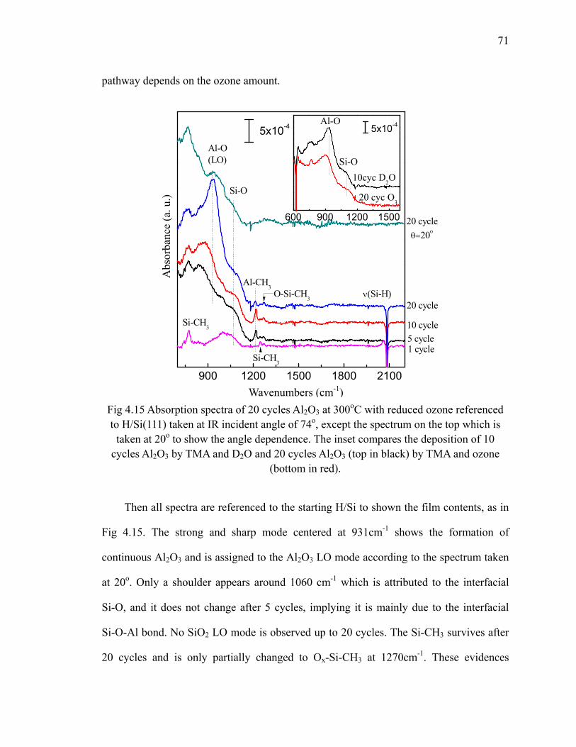
71
pathway depends on the ozone amount.
900 1200 1500 1800 2100
O-Si-CH3
Si-CH3
Si-CH3
5x10⁻⁴
20 cycle θ=20o
20 cycle
10 cycle5 cycle1 cycle
Si-O
Al-O (LO)
ν(Si-H)Al-CH
3
Fig 4.15 Absorption spectra of 20 cycles Al2O3 at 300oC with reduced ozone referenced to H/Si(111) taken at IR incident angle of 74o, except the spectrum on the top which is
taken at 20o to show the angle dependence. The inset compares the deposition of 10 cycles Al2O3 by TMA and D2O and 20 cycles Al2O3 (top in black) by TMA and ozone
(bottom in red).
Then all spectra are referenced to the starting H/Si to shown the film contents, as in
Fig 4.15. The strong and sharp mode centered at 931cm-1 shows the formation of
continuous Al2O3 and is assigned to the Al2O3 LO mode according to the spectrum taken
at 20o. Only a shoulder appears around 1060 cm-1 which is attributed to the interfacial
Si-O, and it does not change after 5 cycles, implying it is mainly due to the interfacial
Si-O-Al bond. No SiO2 LO mode is observed up to 20 cycles. The Si-CH3 survives after
20 cycles and is only partially changed to Ox-Si-CH3 at 1270cm-1. These evidences
600 900 1200 1500
Al-O
Si-O
20 cyc O3
5x10⁻⁴
10cyc D2O
Wavenumbers (cm-1)
Abs
orba
nce
(a. u
.)
72
confirm that Si-O amount is minimal. The featureless spectra in 1300-2100 cm-1 shows
no detectable formate species inside the film consisting with our assumption of a different
reaction pathway.
By comparing the spectrum with that of 10 cycles Al2O3 deposited by TMA and D2O,
as the inset of Fig 4.15, the Al-O and interfacial Si-O modes show similar intensity and
shape. According to the intensity of Al-O phonon mode, the growth rate of the ozone
based Al2O3 is about 1/2 of the water based case, which is in agreement with our ozone
based HfO2 deposition [41] and some studies have shown that the growth rate depends on
the amount of ozone [42]. The film has similar quality for both water and ozone ALD but
definitely ozone ALD has no trapped water inside the film.
4.3 HfO2 deposition using TEMAH/ozone
Since HfO2 has higher dielectric constant than Al2O3 and is being used in the
industrial, it is necessary to study its deposition based on ozone for future applications. In
the following section we will show the deposition HfO2 on H/Si(100) and SiNx.
HfO2 deposited on H/Si(100) by TEMAH/ozone
20 cycles HfO2 are deposited on H/Si(100) by TEMAH and ozone at 100oC, and for
each precursor, saturation exposure time is used. The differential spectra are shown in Fig
4.16. After the first TEMAH dosing, the precursor is chemically adsorbed onto the
surface, evidenced by the loss of Si-H stretching modes at 2000-2200 cm-1, the loss of
dihydride scissor mode at ~912 cm-1 and the appearance of ligand-related modes
including the bands ~1300-1600 cm-1 and CHx stretching modes at 2800-3000 cm-1.
Through the intensity of ν(Si-H), it can be concluded that ~17% H is replaced by

73
TEMAH for the 1st TEMAH dosing. The low H loss is partly due to the bulky ligand
which blocks the reaction sites. The formation of Hf-O-Si band centered at 940 cm-1
suggests the precursor is partially hydrolyzed by the residue water as expected [43].
900 1200 1500 1800 2100 3000
-COH
1st O3
1st TEMAH
ν(CHx)
ν(O-Si-H) ν(Si-H)
δs(Si-H2)
Hf-O-Si
2x10⁻⁴
SiO2
TO/LO
2nd O3
2nd TEMAH
3rd O3
3rd TEMAH
C=ON=O, NO2
Fig 4.16 Differential FTIR spectra of 20 cycles TEMAH and ozone deposition on
H/Si(100) at 100oC. Each spectrum is referenced to that of the surface subjected to the previous treatment. The 1st TEMAH is referenced to H/Si (IR incident angle ~ 74o).
After the 1st ozone exposure, the Si-O TO/LO modes at 1025 cm-1 and 1175 cm-1
imply the forming of continuous SiO2 and the thickness is about 6-7 Å according to the
integrated area. Upon the ozone dosing, the further loss of ν(Si-H) as well as the
formation of Ox-Si-H at 2260 cm-1 consolidates the surface oxidation. The new modes
appear at 1500-1750 cm-1 (at 1585, 1614, 1659, and 1710 cm-1) are possibly attributed to
the carbonyl/nitro derivatives such as C=O, -NO2, N=O stretching and -NH bending
Wavenumbers (cm-1)
Abs
orba
nce
(a. u
.)
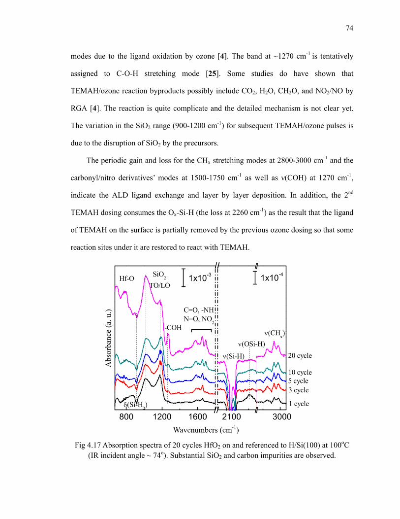
74
modes due to the ligand oxidation by ozone [4]. The band at ~1270 cm-1 is tentatively
assigned to C-O-H stretching mode [25]. Some studies do have shown that
TEMAH/ozone reaction byproducts possibly include CO2, H2O, CH2O, and NO2/NO by
RGA [4]. The reaction is quite complicate and the detailed mechanism is not clear yet.
The variation in the SiO2 range (900-1200 cm-1) for subsequent TEMAH/ozone pulses is
due to the disruption of SiO2 by the precursors.
The periodic gain and loss for the CHx stretching modes at 2800-3000 cm-1 and the
carbonyl/nitro derivatives’ modes at 1500-1750 cm-1 as well as ν(COH) at 1270 cm-1,
indicate the ALD ligand exchange and layer by layer deposition. In addition, the 2nd
TEMAH dosing consumes the Ox-Si-H (the loss at 2260 cm-1) as the result that the ligand
of TEMAH on the surface is partially removed by the previous ozone dosing so that some
reaction sites under it are restored to react with TEMAH.
800 1200 1600 2100 3000
-COH
20 cycle
5 cycle10 cycle
3 cycle
1 cycle
ν(OSi-H)
ν(Si-H)
Hf-O SiO2
TO/LO
δ(Si-H2)
ν(CHx)
C=O, -NHN=O, NO2
1x10⁻³
1x10⁻⁴
Fig 4.17 Absorption spectra of 20 cycles HfO2 on and referenced to H/Si(100) at 100oC (IR incident angle ~ 74o). Substantial SiO2 and carbon impurities are observed.
Wavenumbers (cm-1)
Abs
orba
nce
(a. u
.)
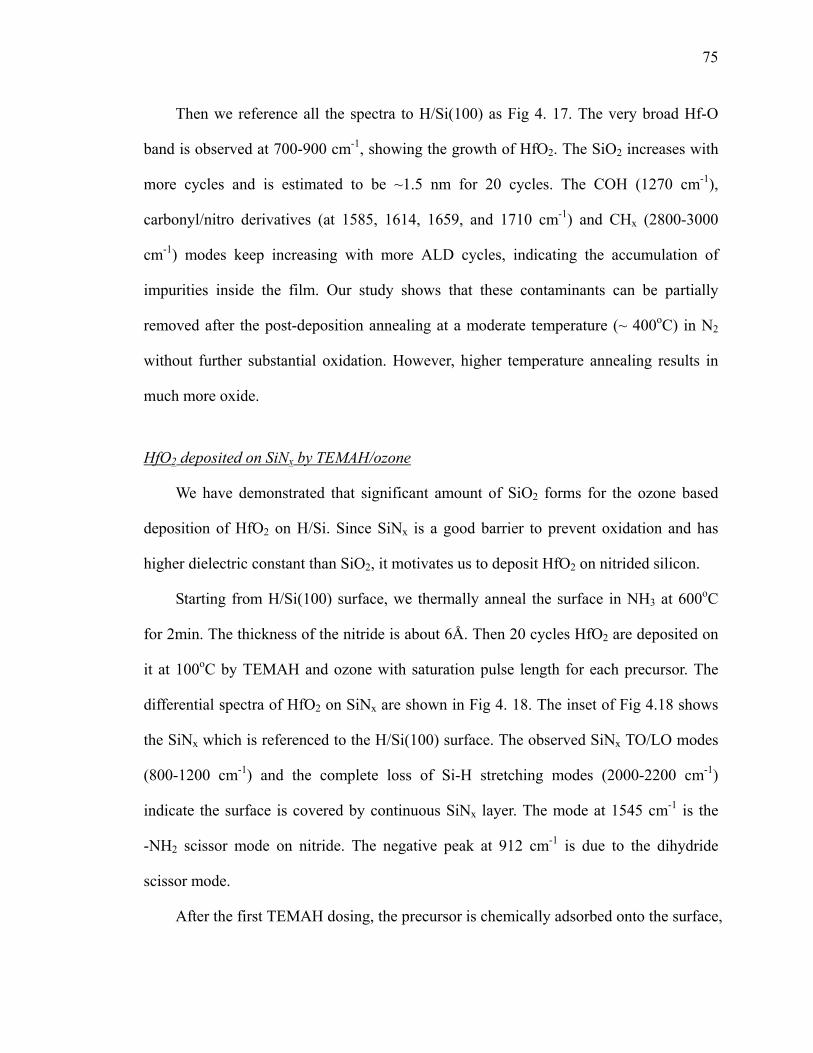
75
Then we reference all the spectra to H/Si(100) as Fig 4. 17. The very broad Hf-O
band is observed at 700-900 cm-1, showing the growth of HfO2. The SiO2 increases with
more cycles and is estimated to be ~1.5 nm for 20 cycles. The COH (1270 cm-1),
carbonyl/nitro derivatives (at 1585, 1614, 1659, and 1710 cm-1) and CHx (2800-3000
cm-1) modes keep increasing with more ALD cycles, indicating the accumulation of
impurities inside the film. Our study shows that these contaminants can be partially
removed after the post-deposition annealing at a moderate temperature (~ 400oC) in N2
without further substantial oxidation. However, higher temperature annealing results in
much more oxide.
HfO2 deposited on SiNx by TEMAH/ozone
We have demonstrated that significant amount of SiO2 forms for the ozone based
deposition of HfO2 on H/Si. Since SiNx is a good barrier to prevent oxidation and has
higher dielectric constant than SiO2, it motivates us to deposit HfO2 on nitrided silicon.
Starting from H/Si(100) surface, we thermally anneal the surface in NH3 at 600oC
for 2min. The thickness of the nitride is about 6Å. Then 20 cycles HfO2 are deposited on
it at 100oC by TEMAH and ozone with saturation pulse length for each precursor. The
differential spectra of HfO2 on SiNx are shown in Fig 4. 18. The inset of Fig 4.18 shows
the SiNx which is referenced to the H/Si(100) surface. The observed SiNx TO/LO modes
(800-1200 cm-1) and the complete loss of Si-H stretching modes (2000-2200 cm-1)
indicate the surface is covered by continuous SiNx layer. The mode at 1545 cm-1 is the
-NH2 scissor mode on nitride. The negative peak at 912 cm-1 is due to the dihydride
scissor mode.
After the first TEMAH dosing, the precursor is chemically adsorbed onto the surface,
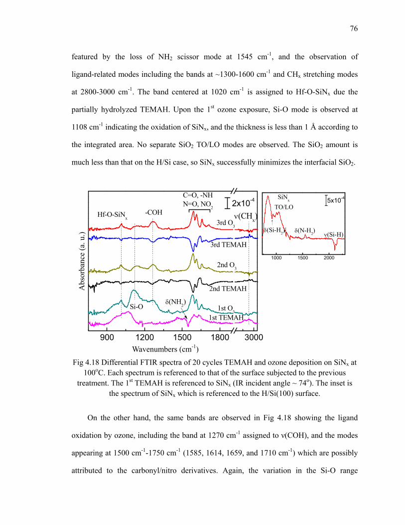
76
featured by the loss of NH2 scissor mode at 1545 cm-1, and the observation of
ligand-related modes including the bands at ~1300-1600 cm-1 and CHx stretching modes
at 2800-3000 cm-1. The band centered at 1020 cm-1 is assigned to Hf-O-SiNx due the
partially hydrolyzed TEMAH. Upon the 1st ozone exposure, Si-O mode is observed at
1108 cm-1 indicating the oxidation of SiNx, and the thickness is less than 1 Å according to
the integrated area. No separate SiO2 TO/LO modes are observed. The SiO2 amount is
much less than that on the H/Si case, so SiNx successfully minimizes the interfacial SiO2.
900 1200 1500 1800 3000
-COH
δ(NH2)
ν(CHx) Hf-O-SiNx
2x10⁻⁴
Si-O 1st O3 1st TEMAH
2nd O3
2nd TEMAH
3rd O3
3rd TEMAH
C=O, -NHN=O, NO2
Fig 4.18 Differential FTIR spectra of 20 cycles TEMAH and ozone deposition on SiNx at
100oC. Each spectrum is referenced to that of the surface subjected to the previous treatment. The 1st TEMAH is referenced to SiNx (IR incident angle ~ 74o). The inset is
the spectrum of SiNx which is referenced to the H/Si(100) surface.
On the other hand, the same bands are observed in Fig 4.18 showing the ligand
oxidation by ozone, including the band at 1270 cm-1 assigned to ν(COH), and the modes
appearing at 1500 cm-1-1750 cm-1 (1585, 1614, 1659, and 1710 cm-1) which are possibly
attributed to the carbonyl/nitro derivatives. Again, the variation in the Si-O range
1000 1500 2000
δ(N-H2) ν(Si-H)
SiNx
TO/LO5x10-4
δ(Si-H2)
Wavenumbers (cm-1)
Abs
orba
nce
(a. u
.)
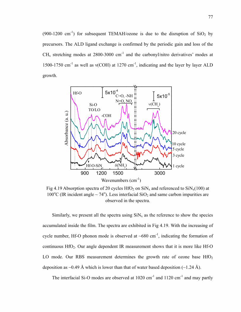
77
(900-1200 cm-1) for subsequent TEMAH/ozone is due to the disruption of SiO2 by
precursors. The ALD ligand exchange is confirmed by the periodic gain and loss of the
CHx stretching modes at 2800-3000 cm-1 and the carbonyl/nitro derivatives’ modes at
1500-1750 cm-1 as well as ν(COH) at 1270 cm-1, indicating and the layer by layer ALD
growth.
900 1200 1500 3000 Hf-O-SiNx
δ(NH2)
5x10⁻⁴Hf-O
Si-O TO/LO
-COH
C=O, -NHN=O, NO2 ν(CHx)
20 cycle
10 cycle5 cycle3 cycle
1 cycle
5x10⁻⁵
Fig 4.19 Absorption spectra of 20 cycles HfO2 on SiNx and referenced to SiNx(100) at 100oC (IR incident angle ~ 74o). Less interfacial SiO2 and same carbon impurities are
observed in the spectra.
Similarly, we present all the spectra using SiNx as the reference to show the species
accumulated inside the film. The spectra are exhibited in Fig 4.19. With the increasing of
cycle number, Hf-O phonon mode is observed at ~680 cm-1, indicating the formation of
continuous HfO2. Our angle dependent IR measurement shows that it is more like Hf-O
LO mode. Our RBS measurement determines the growth rate of ozone base HfO2
deposition as ~0.49 Å which is lower than that of water based deposition (~1.24 Å).
The interfacial Si-O modes are observed at 1020 cm-1 and 1120 cm-1 and may partly
Wavenumbers (cm-1)
Abs
orba
nce
(a. u
.)
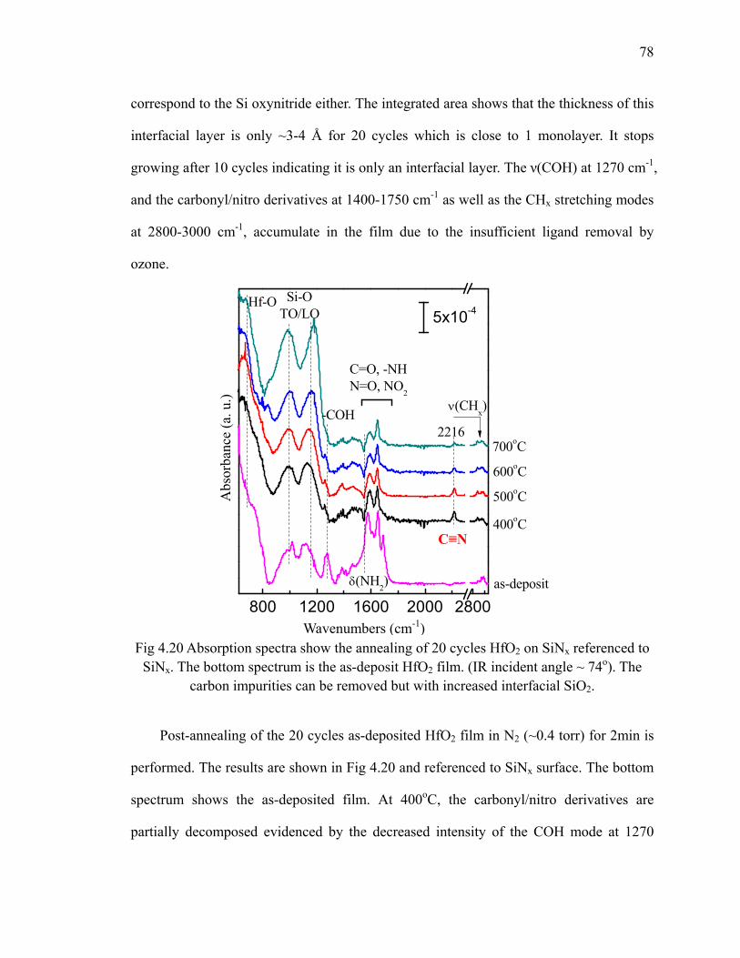
78
correspond to the Si oxynitride either. The integrated area shows that the thickness of this
interfacial layer is only ~3-4 Å for 20 cycles which is close to 1 monolayer. It stops
growing after 10 cycles indicating it is only an interfacial layer. The ν(COH) at 1270 cm-1,
and the carbonyl/nitro derivatives at 1400-1750 cm-1 as well as the CHx stretching modes
at 2800-3000 cm-1, accumulate in the film due to the insufficient ligand removal by
ozone.
800 1200 1600 2000 2800
δ(NH2)
700oC
600oC
500oC
400oC
as-deposit
2216
5x10⁻⁴
-COH
Si-O TO/LO
Hf-O
C=O, -NHN=O, NO2
ν(CHx)
Fig 4.20 Absorption spectra show the annealing of 20 cycles HfO2 on SiNx referenced to
SiNx. The bottom spectrum is the as-deposit HfO2 film. (IR incident angle ~ 74o). The carbon impurities can be removed but with increased interfacial SiO2.
Post-annealing of the 20 cycles as-deposited HfO2 film in N2 (~0.4 torr) for 2min is
performed. The results are shown in Fig 4.20 and referenced to SiNx surface. The bottom
spectrum shows the as-deposited film. At 400oC, the carbonyl/nitro derivatives are
partially decomposed evidenced by the decreased intensity of the COH mode at 1270
C≡N
Wavenumbers (cm-1)
Abs
orba
nce
(a. u
.)
79
cm-1 and the carbonyl/nitro derivatives at (1400-1750 cm-1), and by the partial loss of
CHx stretching modes at 2800-3000 cm-1. However, the bands at 1593 cm-1 and 1646 cm-1
survive even after 700oC annealing, implying some impurities are strongly bonded in the
HfO2. The increasing of Si-O TO/LO modes with the raised temperature is expected
because of the environmental oxygen contamination and the oxygen from the
decomposition of carbonyl/nitro derivatives. The blue shift of SiO2 LO mode (1177 cm-1)
results from the increased SiO2 amount, but it is still much lower than the typical value
(>1200 cm-1). It may indicate that it is not pure SiO2.
Interestingly, a new unexpected mode appears at 2217 cm-1 at 400oC and decreases
upon 600oC annealing. It cannot be attributed to the Si-H stretching mode because our
experiments have shown that Si-H nearly completely decomposes at 600oC. The likely
assignment is ν(C≡N) resulting from the rich N content due to the SiNx layer. The carbon
and nitrogen may rearrange and combine to form nitrile groups at ~400oC because of the
oxygen consumption by SiNx oxidation and the decomposition of the ligand-related
impurities.
4.4 Summary
In this chapter, the ozone based ALD of Al2O3 and HfO2 are investigated for the
future application which can eliminate the trapped water/OH inside the film compared
with water based deposition. However, more complicated reaction mechanism of ozone
based ALD is found and substantial carbon impurities are incorporated during the
deposition, which may affect the final film quality.
For the ozone based Al2O3 by TMA/ozone, the gas phase of TMA is first examined
by in situ FTIR. The TMA in the ALD reactor shows little impurity due to hydrolysis and
80
is in large extent of dimer structure. Then D2O is introduced to the reactor to study the
gas phase reaction between TMA and D2O. This reaction is straightforward and CH4, CD4
are observed as the only byproducts. When ozone is introduced into the TMA gas, the
reaction is much more complicated. Unexpectedly, C2H4 is not the only byproduct and
the oxidation of the methyl terminal group/Al-O-CH3 may prevail which needs further
study.
Al2O3 deposition with long and short ozone pulse length is studied on H/Si(111) at
300oC. In the long pulse case, the cleavage of Al-C bond to form formate is observed by
two unexpected modes at 1400 cm-1 and 1600 cm-1. With the aid of DFT calculation, the
assignments of the new modes are confirmed. Substantial SiO2 interfacial layer is
observed in this case. As for the short ozone pulse case, little interfacial Si-O is observed.
The carbon impurities are trivial as well, indicating an improved film quality which is
comparable to water based deposition. The growth rate is about 1/2 of that of water based
deposition. In addition, no observation of formate species for the short ozone pulse case
suggests a different reaction pathway. Thus, the reaction pathway depends on the ozone
amount.
The ozone based HfO2 ALD is performed on both H/Si (100) and
600oC-thermal-NH3 nitrided H/Si(100) surface at 100oC. On H/Si(100) surface, ozone
substantially oxidizes the surface. Carbonyl and nitro derivatives are observed as the
impurities inside the film, which come from the strong oxidation of ligands by ozone.
Then we deposit HfO2 on SiNx surface by ozone based ALD. The thin nitride (~6Å)
successfully minimizes the formation of interfacial SiO2. However, the film still contains
substantial carbonyl and nitro derivatives. The post-annealing experiment shows that a
moderate temperature annealing at ~400oC can partially eliminate those impurities with
81
slightly increase of SiO2 interfacial layer. Some impurities survive even after 700oC
annealing. More interesting, an unexpected peak at 2217 cm-1, which is possibly due to
the formation of nitrile (-C≡N), is observed after 400oC annealing, indicating the
reorganizing of the film contents. All suggest that the ozone based ALD is a much more
complex system.
Bibliography 1. C. Musgrave and R. G. Gordon, Precursors for atomic layer deposition of high-k dielectrics, Future Fab International 18 (2005), 126-128. 2. J. B. Kim, D. R. Kwon, K. Chakrabarti and C. Lee, Mprovement in Al2O3 dielectric behavior by using ozone as an oxidant for the atomic layer deposition technique, J. Appl. Phys. 92 (2002), 6739. 3. G. D. Wilk, R. M. Wallace and J. M. Anthony, High-k gate dielectrics: Current status and materials properties considerations, Journal of Applied Physics 89 (2001), 5243. 4. X. Liu, S. Ramanathan, A. Longdergan, A. Srivastava, E. Lee, T. E. Seidel, J. T. Barton, b. Dawen Pang and R. G. Gordonb, ALD of hafnium oxide thin films from tetrakis(ethylmethylamino) hafnium and ozone, J. Electrochem. Soc. (2005), 2005. 5. V. R. Rai and S. Agarwal, Surface reaction mechanisms during ozone-based atomic layer deposition of titanium dioxide, J. Phys. Chem. C 112 (2008), 9552. 6. J. Kima, K. Chakrabartia, J. Leeb, K.-Y. Ohc and C. Lee, Effects of ozone as an oxygen source on the properties of the Al2O3 thin films prepared by atomic layer deposition, Mat. Chem. Phys. 78 (2003), 733. 7. J. Hamalainen, M. Kemell, F. Munnik, U. Kreissig, M. Ritala and M. Leskela, Atomic layer deposition of iridium oxide thin films from Ir(acac)3 and ozone Chem. Mat. 20 (2008), 2903. 8. D. H. Triyoso, R. Gregory, M. Park, K. Wang and S. I. Lee, Physical and electrical properties of atomic-layer-deposited HfxZr1-xO2 with TEMAHF, TEMAZr, and ozone, J. Electrochem. Soc. 155 (2008), H43. 9. M. Cho, H. B. Park, J. Park, S. W. Lee, C. S. Hwang, J. Jeong, H. S. Kang and Y. W. Kim, Comparison of properties of an Al2O3 thin layers grown with remote O2 plasma, H2O, or O3 as oxidants in an ald process for HfO2 gate dielectrics, J. Electrochem. Soc. 152 (2005), F49. 10. S. K. Kim, S. W. Lee, C. S. Hwang, Y.-S. Min, J. Y. Won and J. Jeong, Low temperature (<100°c) deposition of aluminum oxide thin films by ALD with O3 as oxidant, J. Electrochem. Soc. 153 (2006), F69. 11. S. Kamiyama, T. Miura and Y. Nara, Electrical properties of ultrathin HfO2 films for replacement metal gate transistors, fabricated by atomic layer deposition using TEMAH
82
and O3, Appl. Phys. Lett. 87 (2005), 132904. 12. M. Juppo, P. Alén, M. Ritala and M. Leskelä, Trimethylaluminum as a reducing agent in the atomic layer deposition of Ti(Al)n thin films, Chemical Vapor Deposition 7 (2001), 211. 13. A. Demchuk, S. Simpson and B. Koplitz, Exploration of the laser-assisted clustering and reactivity of trimethylaluminum with and without NH3, J. Phys. Chem. A 107 (2003), 1727. 14. H. M. Manasevit, The use of metal-organics in the preparation of semiconductor materials, J. Electrochem. Soc. 118 (1971), 647. 15. R. Anwander, C. Palm, O. Groeger and G. Engelhardt, Formation of Lewis acidic support materials via chemisorption of trimethylaluminum on mesoporous silicate MCM-41 Organometallics 17 (1998), 2027. 16. J. Schmidt, T. Risse, H. Hamann and H.-J. Freund, Characterization of a model ziegler-natta catalyst for ethylene polymerization, J. Chem. Phys. 116 (2002), 10861. 17. S. Balasubramanian, C. J. Mundy and M. L. Klein, Trimethylaluminum: A computer study of the condensed phases and the gas dimer, J. Phys. Chem. B 102 (1998), 10136. 18. J. Tanaka and S. R. Smith, Mass spectra of bridge-bonded aluminum compounds, Inorganic Chemistry 8 (1968), 265. 19. A. W. Laubengayer and W. F. Gilliam, The alkyls of the third-group elements. I. Vapor-phase studies of the alkyls of aluminum, gallium and indium, J. Am. Chem. Soc. 63 (1941), 477. 20. T. Shinzawa1, F. Uesugi, I. Nishiyama, K. Sugai1, S. Kishida and H. Okabayashi, New molecular compound precursor for aluminum chemical vapor deposition, Appl. Organometal. Chem. 14 (2000), 14. 21. B. G. Willis and K. F. Jensen, An evaluation of density functional theory and ab initio predictions for bridge-bonded aluminum compounds, J. Phys. Chem. A 102 (1998), 2613. 22. R. J. O'Brien and G. A. Ozin, A gas-phase Raman study of trimethylaluminium and trimethylboron monomers, J. Chem. Soc. A (1971), 1136. 23. C. Soto, R. Wu, D. W. Bennett and W. T. Tysoe, Infrared spectroscopy of trimethylaluminum and dimethylaluminum chloride adsorbed on alumina, Chem. Mat. 6 (1994), 1705. 24. M. Sugiyama, H. Itoh, J. Aoyama, H. Komiyama and Y. Shimogaki, Reaction analysis of aluminum chemical vapor deposition from dimethyl-aluminum-hydride using tubular reactor and Fourier-transform infrared spectroscopy: Theoretical process optimization procedure (1), Jpn. J. Appl Phys. 39 (2000), 1074. 25. G. Socrates, Infrared and Raman characteristic group frequencies, 3rd edition, John Wiley & Sons (2006). 26. S. D. Elliott, G. Scarel, C. Wiemer, M. Fanciulli and G. Pavia, Ozone-based atomic layer deposition of alumina from TMA: Growth, morphology, and reaction mechanism, Chem. Mater. 18 (2006), 3764. 27. R. L. Puurunen, Growth per cycle in atomic layer deposition: Real application
83
examplesof a theoretical model, Chemical Vapor Deposition 9 (2003), 327. 28. M. M. Frank, Y. J. Chabal and G. D. Wilk, Nucleation and interface formation mechanisms in atomic layer deposition of gate oxides, Appl. Phys. Lett. 82 (2003), 4758. 29. M. D. Halls, K. Raghavachari, M. M. Frank and Y. J. Chabal, Atomic layer deposition of Al2O3 on H-passivated Si: Al(CH3)2OH surface reactions with H/Si(100)-2×1, Phys. Rev. B 68 (2003), 161302. 30. J. Kwon, M. Dai, M. D. Halls and Y. J. Chabal, Detection of a formate surface intermediate in the atomic layer deposition of high-κ dielectrics using ozone, Chem. Mat. 20 (2008), 3248. 31. V. Boiadjiev and W. T. Tysoe, Infrared study of the surface species formed by sequential chemical vapor deposition of trimethylaluminum and methanol on a hydroxylated alumina surface Chem. Mat. 10 (1998), 334. 32. D. N. Goldstein and S. M. George, Conference program of the 6th international conference on atomic layer deposition, Seoul, South Korea; American Vacuum Society: New York (2006). 33. G. A. M. Hussein and N. Sheppard, Infrared spectroscopic studies of the reactions of alcohols over group IVB metal oxide catalysts, J. Chem. Soc. Faraday Trans. 87 (1991), 2655. 34. B. Delley, From molecules to solids with the Dmol3 approach, J. Chem. Phys. 113 (2000), 7756. 35. J. P. Perdew, K. Burke and M. Ernzerhof, Generalized gradient approximation made simple, Phys. Rev. Lett. 77 (1996), 3865. 36. G. Prechtl, A. Kersch, G. S. Icking-Konert, W. Jacobs, T. Hecht, H. Boubekeur and U. Schröder, A model for Al2O3 ALD conformity and deposition rate from oxygen precursor reactivity, IEEE Int. Electron Devices 9 (2003), 9.6.1. 37. K. T. Queeney, N. Herbots, J. M. Shaw, V. Atluri and Y. J. Chabal, Infrared spectroscopic analysis of an ordered Si/SiO2 interface, Appl. Phys. Lett. 84 (2004), 493. 38. D. N. Goldstein, J. A. McCormick and S. M. George, Al2O3 atomic layer deposition using trimethylaluminum and ozone studied by in situ transmission FTIR spectroscopy and quadrupole mass spectrometry, J. Phys. Chem. C (2008). 39. G. P. Shulman, M. Trusty and J. H. Vickers, Thermal decomposition of aluminum alkoxides, J. Org. Chem. 28 (1963), no. 4, 907-910. 40. J. A. Aboaf, Deposition and properties of aluminum oxide obtained by pyrolytic decomposition of an aluminum alkoxide, Journal of The Electrochemical Society 114 (1967), no. 9, 948-952. 41. Y. Wang, M. Dai, M.-T. Ho, L. S. Wielunski and Y. J. Chabal, Infrared characterization of hafnium oxide grown by atomic layer deposition using ozone as the oxygen precursor, Appl. Phys. Lett. 90 (2007), 022906. 42. J. Kima, K. Chakrabartia, J. Leeb, K.-Y. Ohc and C. Lee, Effects of ozone as an oxygen source on the properties of the Al2O3 thin films prepared by atomic layer deposition, Mat. Chem. Phys. 78 (2003), 733.
84
43. M.-T. Ho, Y. Wang, R. T. Brewer, L. S. Wielunski and Y. J. Chabal, In situ infrared spectroscopy of hafnium oxide growth on hydrogen-terminated silicon surfaces by atomic layer deposition, Appl. Phys. Lett. 87 (2005), 133103.
85
Chapter 5: La2O3 and LaxAlyO Growth on H/Si by ALD
Lanthanum oxide (La2O3) is widely used in industry and laboratory. It has been used
to make optical glasses to improve the refractive index and chemical durability [1, 2, 3].
It can also be used to develop ferroelectric materials [4, 5]. Since La2O3 has the largest
band gap among the rare earth oxides (~4.3 eV) with the lowest lattice energy, very high
dielectric constant (~ 27) and good thermal stability on Si [6, 7, 8], it is also a candidate
to replace SiO2 as an insulator material [6, 9, 10]. La2O3 films can be obtained by many
different methods, such as chemical vapor deposition, thermal oxidation, sputtering, and
so on [1, 2, 3, 11, 12, 13].
Due to its great advantages equivalent to or over other methods such as uniformity
and high quality, ALD is being used to deposit La2O3 as well. In the following part of this
chapter, we will study the ALD of La2O3 film by using a brand new precursor [14],
lanthanum tris (N,N’- diisopropylacetamidinate) [La(iPr-MeAMD)3] and heavy water
(D2O). The precursor ALD temperature window, reaction mechanism and film quality
will be investigated. The deposition of lanthanum aluminate film on H/Si will be studied
also.
5.1 Lanthanum precursor gas phase La(iPr-MeAMD)3 precursor has high volatility (80oC/0.04 torr) among most of
known lanthanum precursors [15], and has been successfully demonstrated for ALD [16].
The chemical structure of La(iPr-MeAMD)3 precursor is shown in Fig. 5.1 with its
ball-stick three dimensional view. It is thermally stable enough and the metal-N bond has
low bond strength compared with metal-Cl and metal-O bonds to make it highly reactive
with water [14, 17]. On the other hand, the metal-N bond causes fewer impurities than the

86
metal-C bond during the deposition. Thus, it is a suitable precursor for ALD. To have as
high as possible vapor pressure for ALD, the precursor is kept at ~130oC for all
experiments. Purified N2 (oxygen impurity <10-6 ppm) is used as the carrying gas to
deliver more precursor to the ALD reactor.
Fig 5.1 Chemical structure of La(iPr-MeAMD)3 precursor and its ball-stick three
dimensional view used to deposite La2O3
800 1200 1600 2800 3200 3600
La-pre
ν(ND)
ν(C
C) ν(C
N)
ν(N
CN
)
δ s(CH
3)δ(
CH
)
ν(N=C)
ν s(CH
)ν s(C
H3)
ν as(C
H3)
1x10⁻²
ν(N
H)
D2O
Fig 5.2 FTIR absorption spectrum of gas phase La(iPr-MeAMD)3 (top in black)
referenced to vacuum and the spectrum after exposed to D2O (bottom in red) referenced to the La precursor showing the gas phase reaction.
Before the ALD of La2O3, the precursor gas phase is first examined to know the
N N
N
N
La
N
N
Abs
orba
nce
(a. u
.)
Wavenumbers (cm-1)
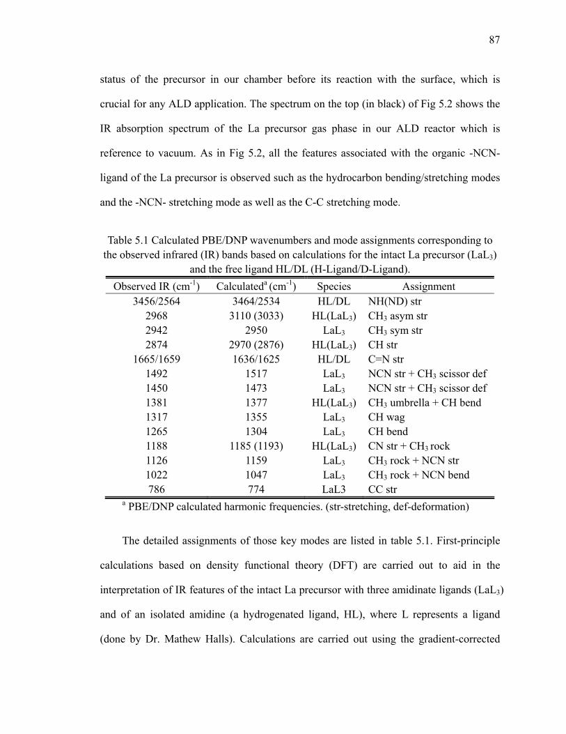
87
status of the precursor in our chamber before its reaction with the surface, which is
crucial for any ALD application. The spectrum on the top (in black) of Fig 5.2 shows the
IR absorption spectrum of the La precursor gas phase in our ALD reactor which is
reference to vacuum. As in Fig 5.2, all the features associated with the organic -NCN-
ligand of the La precursor is observed such as the hydrocarbon bending/stretching modes
and the -NCN- stretching mode as well as the C-C stretching mode.
Table 5.1 Calculated PBE/DNP wavenumbers and mode assignments corresponding to
the observed infrared (IR) bands based on calculations for the intact La precursor (LaL3) and the free ligand HL/DL (H-Ligand/D-Ligand).
Observed IR (cm-1) Calculateda (cm-1) Species Assignment 3456/2564 3464/2534 HL/DL NH(ND) str
2968 3110 (3033) HL(LaL3) CH3 asym str 2942 2950 LaL3 CH3 sym str 2874 2970 (2876) HL(LaL3) CH str
1665/1659 1636/1625 HL/DL C=N str 1492 1517 LaL3 NCN str + CH3 scissor def1450 1473 LaL3 NCN str + CH3 scissor def1381 1377 HL(LaL3) CH3 umbrella + CH bend 1317 1355 LaL3 CH wag 1265 1304 LaL3 CH bend 1188 1185 (1193) HL(LaL3) CN str + CH3 rock 1126 1159 LaL3 CH3 rock + NCN str 1022 1047 LaL3 CH3 rock + NCN bend 786 774 LaL3 CC str
a PBE/DNP calculated harmonic frequencies. (str-stretching, def-deformation)
The detailed assignments of those key modes are listed in table 5.1. First-principle
calculations based on density functional theory (DFT) are carried out to aid in the
interpretation of IR features of the intact La precursor with three amidinate ligands (LaL3)
and of an isolated amidine (a hydrogenated ligand, HL), where L represents a ligand
(done by Dr. Mathew Halls). Calculations are carried out using the gradient-corrected

88
PBE functional [18] as implemented in the DMol3 package [19]. A numerical atomic
basis set of double-ζ quality, augmented with additional polarization functions (DNP)
with a real-space cutoff of 5.8 Å is employed. For La the core electrons are represented
with an effective relativistic semi-core pseudopotential (PSPP) along with the DNP basis
for valence electrons [20]. The convergence criteria for structural optimizations are
1.0×10⁻⁷ au and 1.0×10⁻⁵ au/Å for energy and gradient, respectively
Note that in the IR spectrum of the La precursor gas phase, the strong mode at 1665
cm-1 and the weak mode at 3456 cm-1 are assigned to ν(C=N) and ν(N-H) in the
hydrogenated ligand H-Ligand, respectively. However, they are not part of the intact
precursor. When the chelated ligand of the precursor is intact, the π-electrons within the
bond of the N-C-N linkage are delocalized, leading to a mode at 1492 cm-1. When the
precursor is hydrolyzed to form the localized C=N in the HN-C=N bond, the band at
1492 cm-1 will be shifted to 1665 cm-1 (calc. 1636 cm-1) with the stretching mode of N-H
at 3456 cm-1. In addition, our real-time mass spectroscopy of the ALD reactor confirms
that a gas phase molecule with atomic mass 142 is observed, which corresponds to the
HL species. Since HL is non-reactive, it remains in the gas phase and is preferentially
detected by mass spectroscopy. It also does not affect film growth during the ALD
process which we will show later.
To further prove this process and study the preliminary of ALD reaction mechanism,
D2O is introduced into the chamber with La precursor to investigate the gas phase
reaction. In Fig 5.2, the spectrum at the bottom (in red) shows the spectral changes
(referenced to La precursor) occurring after the lanthanum precursor is exposed to water
(D2O). Most of the methyl-related bands of the La(iPr-MeAMD)3 precursor lose their
intensity, and some new bands are observed between 1300 and 1430 cm-1 after the D2O
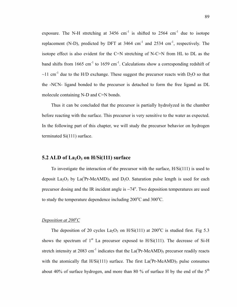
89
exposure. The N-H stretching at 3456 cm-1 is shifted to 2564 cm-1 due to isotope
replacement (N-D), predicted by DFT at 3464 cm-1 and 2534 cm-1, respectively. The
isotope effect is also evident for the C=N stretching of N-C=N from HL to DL as the
band shifts from 1665 cm-1 to 1659 cm-1. Calculations show a corresponding redshift of
~11 cm-1 due to the H/D exchange. These suggest the precursor reacts with D2O so that
the -NCN- ligand bonded to the precursor is detached to form the free ligand as DL
molecule containing N-D and C=N bonds.
Thus it can be concluded that the precursor is partially hydrolyzed in the chamber
before reacting with the surface. This precursor is very sensitive to the water as expected.
In the following part of this chapter, we will study the precursor behavior on hydrogen
terminated Si(111) surface.
5.2 ALD of La2O3 on H/Si(111) surface
To investigate the interaction of the precursor with the surface, H/Si(111) is used to
deposit La2O3 by La(iPr-MeAMD)3 and D2O. Saturation pulse length is used for each
precursor dosing and the IR incident angle is ~74o. Two deposition temperatures are used
to study the temperature dependence including 200oC and 300oC.
Deposition at 200oC
The deposition of 20 cycles La2O3 on H/Si(111) at 200oC is studied first. Fig 5.3
shows the spectrum of 1st La precursor exposed to H/Si(111). The decrease of Si-H
stretch intensity at 2083 cm-1 indicates that the La(iPr-MeAMD)3 precursor readily reacts
with the atomically flat H/Si(111) surface. The first La(iPr-MeAMD)3 pulse consumes
about 40% of surface hydrogen, and more than 80 % of surface H by the end of the 5th
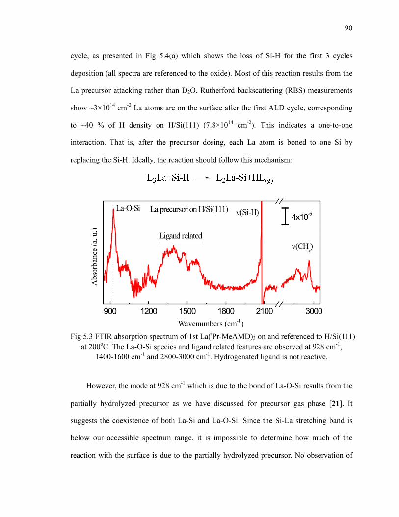
90
cycle, as presented in Fig 5.4(a) which shows the loss of Si-H for the first 3 cycles
deposition (all spectra are referenced to the oxide). Most of this reaction results from the
La precursor attacking rather than D2O. Rutherford backscattering (RBS) measurements
show ~3×1014 cm-2 La atoms are on the surface after the first ALD cycle, corresponding
to ~40 % of H density on H/Si(111) (7.8×1014 cm-2). This indicates a one-to-one
interaction. That is, after the precursor dosing, each La atom is boned to one Si by
replacing the Si-H. Ideally, the reaction should follow this mechanism:
900 1200 1500 1800 2100 3000
La precursor on H/Si(111)
ν(CHx)
ν(Si-H)
Ligand related
4x10⁻⁵La-O-Si
Fig 5.3 FTIR absorption spectrum of 1st La(iPr-MeAMD)3 on and referenced to H/Si(111)
at 200oC. The La-O-Si species and ligand related features are observed at 928 cm-1, 1400-1600 cm-1 and 2800-3000 cm-1. Hydrogenated ligand is not reactive.
However, the mode at 928 cm-1 which is due to the bond of La-O-Si results from the
partially hydrolyzed precursor as we have discussed for precursor gas phase [21]. It
suggests the coexistence of both La-Si and La-O-Si. Since the Si-La stretching band is
below our accessible spectrum range, it is impossible to determine how much of the
reaction with the surface is due to the partially hydrolyzed precursor. No observation of
Abs
orba
nce
(a. u
.)
Wavenumbers (cm-1)
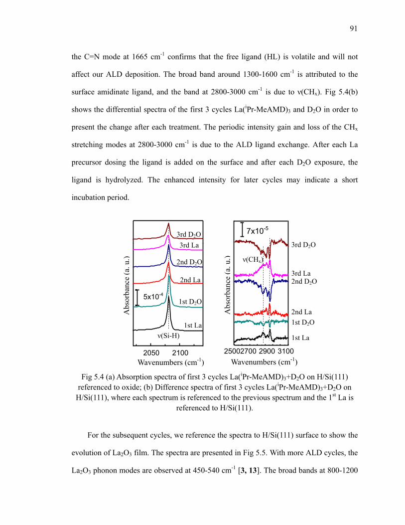
91
the C=N mode at 1665 cm-1 confirms that the free ligand (HL) is volatile and will not
affect our ALD deposition. The broad band around 1300-1600 cm-1 is attributed to the
surface amidinate ligand, and the band at 2800-3000 cm-1 is due to ν(CHx). Fig 5.4(b)
shows the differential spectra of the first 3 cycles La(iPr-MeAMD)3 and D2O in order to
present the change after each treatment. The periodic intensity gain and loss of the CHx
stretching modes at 2800-3000 cm-1 is due to the ALD ligand exchange. After each La
precursor dosing the ligand is added on the surface and after each D2O exposure, the
ligand is hydrolyzed. The enhanced intensity for later cycles may indicate a short
incubation period.
Fig 5.4 (a) Absorption spectra of first 3 cycles La(iPr-MeAMD)3+D2O on H/Si(111) referenced to oxide; (b) Difference spectra of first 3 cycles La(iPr-MeAMD)3+D2O on
H/Si(111), where each spectrum is referenced to the previous spectrum and the 1st La is referenced to H/Si(111).
For the subsequent cycles, we reference the spectra to H/Si(111) surface to show the
evolution of La2O3 film. The spectra are presented in Fig 5.5. With more ALD cycles, the
La2O3 phonon modes are observed at 450-540 cm-1 [3, 13]. The broad bands at 800-1200
2050 2100
5x10⁻⁴
ν(Si-H)
25002700 2900 3100
7x10⁻⁵
ν(CHx)
1st La
1st D2O
2nd La
2nd D2O
3rd La3rd D2O
1st La
1st D2O 2nd La
2nd D2O 3rd La
3rd D2O
Abs
orba
nce
(a. u
.)
Wavenumbers (cm-1)
Abs
orba
nce
(a. u
.)
Wavenumbers (cm-1)
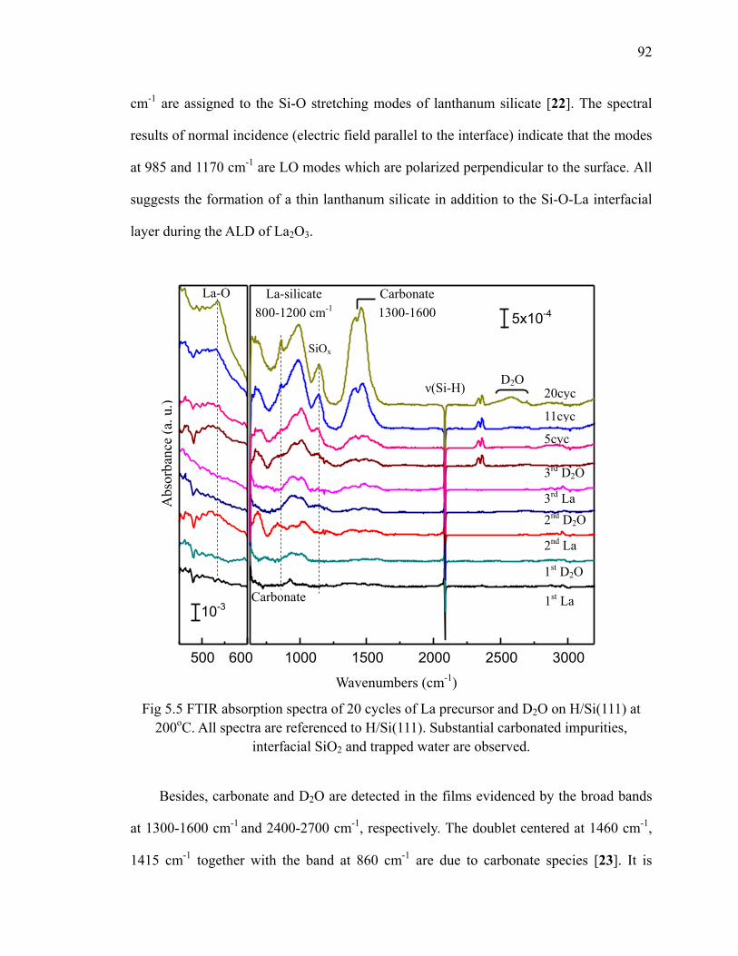
92
cm-1 are assigned to the Si-O stretching modes of lanthanum silicate [22]. The spectral
results of normal incidence (electric field parallel to the interface) indicate that the modes
at 985 and 1170 cm-1 are LO modes which are polarized perpendicular to the surface. All
suggests the formation of a thin lanthanum silicate in addition to the Si-O-La interfacial
layer during the ALD of La2O3.
Fig 5.5 FTIR absorption spectra of 20 cycles of La precursor and D2O on H/Si(111) at 200oC. All spectra are referenced to H/Si(111). Substantial carbonated impurities,
interfacial SiO2 and trapped water are observed.
Besides, carbonate and D2O are detected in the films evidenced by the broad bands
at 1300-1600 cm-1 and 2400-2700 cm-1, respectively. The doublet centered at 1460 cm-1,
1415 cm-1 together with the band at 860 cm-1 are due to carbonate species [23]. It is
1000 1500 2000 2500 3000 500 600
10-3
ν(Si-H)
1st La
1st D2O
2nd La
2nd D2O 3rd La
3rd D2O
5cyc
11cyc
20cyc
La-silicate 800-1200 cm-1
5x10⁻⁴
Carbonate 1300-1600
La-O
D2O
Carbonate
Abs
orba
nce
(a. u
.)
Wavenumbers (cm-1)
SiOx
93
known that La2O3 can react with ambient CO2, resulting in carbonate species [2, 12, 24,
25, 26, 27, 28]. However, since all our ALD process is performed in situ in vacuum
chamber with N2, the observed carbonate present in the film must originate from intrinsic
surface reactions. It is likely that lanthanum carbonate is produced through the thermal
decomposition of lanthanum acetate. There is in fact possible evidence of some acetate
species present on the surface, characterized by the broad bands at 600-700 cm-1 and
2800-3000 cm-1 [29]. The areas under these bands (and the bands between 1300 and 1600
cm-1) grow almost linearly with the number of ALD cycles.
As in Fig 5.6(a), the differential spectra for each half-cycle clearly shows that the
intensity of these vibrational modes increases after D2O pulses rather than after
La(iPr-MeAMD)3 pulses. It suggests that these carbonate bands arise from reactions
between D2O and the remaining amidinate ligand. The possible reaction scheme is
described by the following two steps:
Some of the resulting acetate ions are likely to remain in the film as impurities because
the lanthanum acetate bond is roughly as strong as a lanthanum-hydroxyl bond. Thus
there is little thermodynamic driving force to hydrolyze the acetate ions to acetic acid,
which would vaporize off the surface. And then part of lanthanum acetate is thermally
decomposed into lanthanum carbonate as the observed strong doublet centered at 1460

94
cm-1 and 1415 cm-1 as well as the band at 860 cm-1.
After the deposition, in situ post-deposition annealing in N2 for 5 min from
400-800oC is performed. The spectral results are shown in Fig 5.6(b) where the spectra
are referenced to H/Si and the bottom spectrum is the 20 cycles La2O3 as-deposit film. At
500oC, the carbonate species are almost completely removed as evidenced by the loss of
carbonate broad bands at 1300-1600cm-1. However, the resulted excessive oxygen from
the decomposition of carbonate species and trapped D2O in La2O3 cause the oxidation [30]
of Si interface featured by the broad peaks at 900-1200 cm-1 (TO/LO modes of SiO2
[31]).
Fig 5.6 (a) Differential spectra of 19th cycle and 20th cycle La2O3 deposition in the carbonate range; (b) the absorption spectra showing the post annealing of 20 cycles La2O3 in N2 which are reference to the H/Si(111). The spectra shows ALD ligand
exchange and removal of carbonate species.
Deposition at 300oC
1200 1400 1600
1x10⁻⁴ Carbonate
800 1200 1600
2x10⁻³
Carbonate
SiO2
300 oC 400 oC 500 oC
600 oC
700 oC
800 oC
as-deposit 19th La
19th D2O
20th La
20th D2O
Abs
orba
nce
(a. u
.)
Wavenumbers (cm-1)
Abs
orba
nce
(a. u
.)
Wavenumbers (cm-1)

95
The above experiments show that at 200oC the deposited film contains substantial
amount of impurities including acetate/carbonate and D2O. These impurities can be
substantially reduced by thermal annealing at a moderate temperature (≤ 400oC) without
much increasing the interfacial SiO2 layer. So a higher deposition temperature, 300oC is
used to deposit La2O3 with the same condition as 200oC. The results are presented in Fig
5.7.
As in Fig 5.7, at 300oC, the intensities of bands at 1300-1600 cm-1 and 2800-3000
cm-1 for acetate/carbonate, and at 2400-2700 cm-1 for D2O are suppressed substantially.
According to the drastic loss of Si-H stretching mode at 2083 cm-1, Si-H reacts with surface
hydrogen very strongly at 300 oC, where almost all Si-H bonds are consumed in 5 ALD
cycles. And with more ALD cycles, the observed La2O3 phonon modes at 450-540 cm-1
confirm the formation of La2O3 layer. Although the amount of interfacial SiO2 is increased
compared to the deposition at 200oC (~ 100% increase), the total amount of that interfacial
layer is estimated to be ~ 3 Å according to the integrated area of SiO2. These observations
suggest that 300oC is a better deposition temperature for La2O3 growth.
Note that in Fig 5.7 there are two new features at 1990 and 2110 cm-1 observed
during the deposition at 300oC. As in Fig 5.8 (differential spectra of the first 3 cycles),
their intensities are increased after each La precursor pulse, and then dramatically
reduced after each D2O pulse. Although the frequencies of these two bands are within the
range of Si-H stretching mode, but their integrated areas are much greater than that of the
initial Si-H stretching mode. Since only C, N, H, D, and O are involved in the film, their
origin is very likely related to C and N. They can be either assigned to stretching
vibration of the triple bond (C≡N) in the cyanamide (N-C≡N)2-, or to the double bond
(C=N) in the carbodiimide (N=C=N)2- [32, 33].
96
Fig 5.7 FTIR absorption spectra of 20 cycles of La precursor and D2O on H/Si(111) at
300oC. All spectra are referenced to H/Si(111). Less carbonated species and less D2O are observed. But the interfacial SiO2 increases substantially.
The formation of the cyanamide (or carbodiimide) species on the surface may be
attributed to precursor ligand decomposition at 300oC and probably through β- or
δ-hydrogen transfer within the ligand. Fig 5.9 shows the possible decomposition
pathways from intact ligand to cyanamide. β-hydrogen transfers to form NH bonds in the
ligand and propene (C3H6) is produced as a gas phase byproduct. N≡C triple bonds are
produced through the second β-hydrogen transfer with methane (CH4) as a gas phase
byproduct. This N≡C triple bond can also be formed directly through δ-hydrogen
transfers from the intact ligand on the surface. Finally cyanamide is formed through
additional β-hydrogen transfers with propene as a byproduct which is pumped off without
2nd D2O
1st D2O
800 1200 1600 2400 2800
5x10⁻⁴
2000500 550 600
10-3
ν(Si-H) (D2O)
La- silicate
SiOx
Carbonatespecies
La-O
1st La
2nd La
3rd D2O 3rd La
5cyc
11th D2O20 cyc
ν(CH3)
11th La
10 cyc
Abs
orba
nce
(a. u
.)
Wavenumbers (cm-1)
97
10-4
1900 2000 2100 2200
1st D2O
2nd La
2nd D2O
3rd La
3rd D2O
1st La
1990 cm-1 2110 cm-1
further interaction with the surface.
Fig 5.8 Differential spectra of the first 3 cycles of La precursor and D2O on H/Si(111) at
300oC, where each spectrum is referenced to the previous spectrum and the 1st La is referenced to H/Si(111), and the exchange of the decomposed ligands with D2O is
observed as well.
Generally, the precursor ligand decomposition on the surface leads to further
reaction among precursor molecules during the precursor dosing, and thereby destroys
the self-limitation of the ALD reaction. However, in this case the La precursor with
decomposed ligand is not reactive with other La precursor molecules, and then the
decomposed ligand is removed from the surface by the subsequent water pulse, as
evidenced by the loss of the intensity at 1990 and 2110 cm-1 as shown by the differential
spectra in Fig 5.8. Thus the self-termination property of the precursor will not be affected
by the ligand decomposition. In fact, the smaller decomposed ligand facilitates access of
more precursor molecules to the surface (smaller steric interactions), speeding up the film
growth.
Abs
orba
nce
(a. u
.)
Wavenumbers (cm-1)
98
Fig 5.9 Possible decomposition pathways from intact precursor ligand to cyanamide (proposed by Prof. Roy Gordon). The actual pathway is not clear yet.
5.3 Miscellany of La(iPr-MeAMD)3 ALD temperature window
Lanthanum oxide is known to be highly hygroscopic [25, 34]. During the ALD
process, it can slowly absorb water either from the ambient or when exposed to water,
forming lanthanum hydroxide. Lanthanum hydroxide then slowly desorbs -OH during
lanthanum precursor exposures. CVD-like reaction can thus happen and destroys the
ALD self terminating condition [16].
One example is shown in Fig 5.10, where the H/Si(111) surface is exposed to the La
precursor several times continuously at 300oC. After each dosing of La precursor at
300oC, we cool down the sample and take IR spectra which will take about 1 hour, and
then increase the temperature to expose the surface to La precursor again. This process
repeats and Fig 5.10 shows the differential spectra of the effect of multiple dosing. After
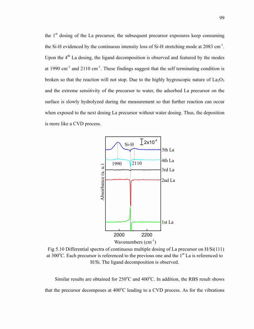
99
the 1st dosing of the La precursor, the subsequent precursor exposures keep consuming
the Si-H evidenced by the continuous intensity loss of Si-H stretching mode at 2083 cm-1.
Upon the 4th La dosing, the ligand decomposition is observed and featured by the modes
at 1990 cm-1 and 2110 cm-1. These findings suggest that the self terminating condition is
broken so that the reaction will not stop. Due to the highly hygroscopic nature of La2O3
and the extreme sensitivity of the precursor to water, the adsorbed La precursor on the
surface is slowly hydrolyzed during the measurement so that further reaction can occur
when exposed to the next dosing La precursor without water dosing. Thus, the deposition
is more like a CVD process.
2000 2200
5th La
4th La
3rd La
2nd La
1st La
21101990
2x10⁻⁴Si-H
Fig 5.10 Differential spectra of continuous multiple dosing of La precursor on H/Si(111) at 300oC. Each precursor is referenced to the previous one and the 1st La is referenced to
H/Si. The ligand decomposition is observed.
Similar results are obtained for 250oC and 400oC. In addition, the RBS result shows
that the precursor decomposes at 400oC leading to a CVD process. As for the vibrations
Abs
orba
nce
(a. u
.)
Wavenumbers (cm-1)

100
of ligand decomposition at 1990 cm-1 and 2110 cm-1, they show the minimum intensity at
300oC. When temperature goes below 200oC, precursor physisorption is observed on the
surface frequently. Thereby, the deposition of La2O3 is not a well defined ALD process in
our ALD reactor. Ex situ RBS didn’t show a clear relation between the deposition rate
and temperatures or between the deposition rate and cycle numbers. The film is not
uniform and the growth rate somehow is quite random. 300oC appears to be the best
choice for the deposition temperature.
5.4 ALD of LaxAlyO on H/Si(111) surface
Now we are in dilemma: at low temperature (< 250-300oC) deposition, substantial
amount of carbonate species and D2O exists inside the film or physi-sorption occurs;
while at 250-300oC the deposition somehow is more CVD-like due to the trapped
water/OH by lanthanum oxide. Study has shown that the water adsorption/desorption
problems due to the hygroscopic nature of La2O3 can be overcome by deposition of
alternating layers of La2O3 and Al2O3, which remains the high dielectric constant [9, 16].
Thus, LaxAlyO nanolaminate is deposited on H/Si(111) in our ALD reactor to have
reaction mechanistic study by in situ FTIR.
During the deposition of LaxAlyO, a full cycle of TMA/D2O is introduced after
every La(iPr-MeAMD)3/D2O cycle and saturation pulse length is used for each precursor
dosing. Fig 5.11 shows the differential spectra of H/Si(111) exposed to alternating
La2O3/Al2O3 ALD cycles at 300oC, where each odd number of cycle is La2O3 cycle and
each even number of cycle is Al2O3 cycle.
The 1st La exposure shows the same features as we have discussed previously. Upon
the subsequent 1st D2O, interfacial SiO2 is observed at this temperature in addition to the
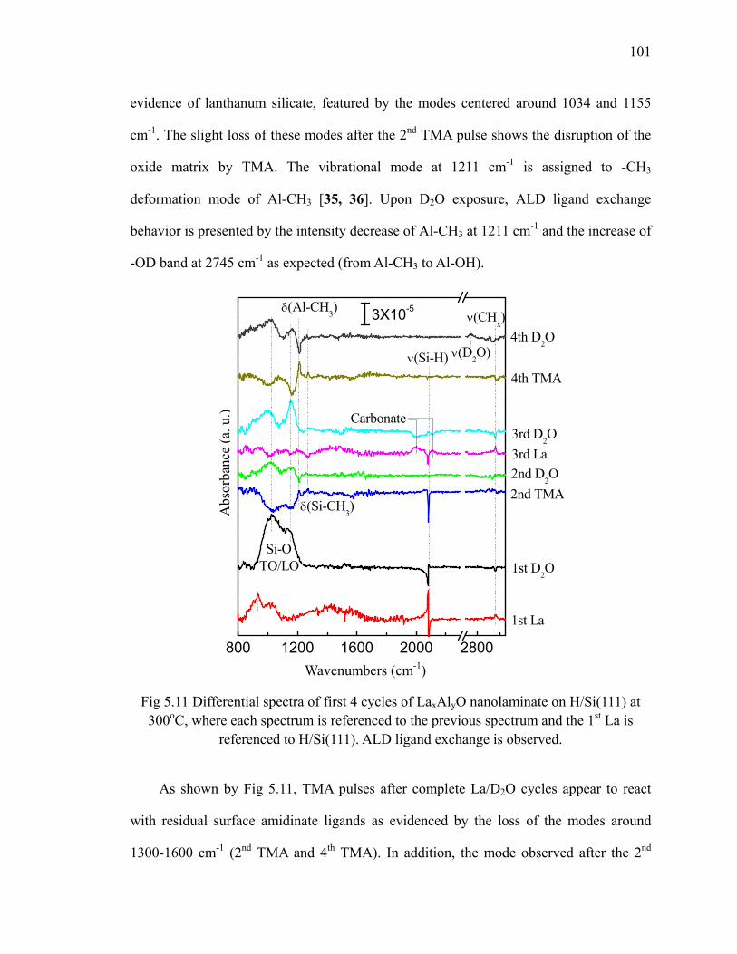
101
evidence of lanthanum silicate, featured by the modes centered around 1034 and 1155
cm-1. The slight loss of these modes after the 2nd TMA pulse shows the disruption of the
oxide matrix by TMA. The vibrational mode at 1211 cm-1 is assigned to -CH3
deformation mode of Al-CH3 [35, 36]. Upon D2O exposure, ALD ligand exchange
behavior is presented by the intensity decrease of Al-CH3 at 1211 cm-1 and the increase of
-OD band at 2745 cm-1 as expected (from Al-CH3 to Al-OH).
800 1200 1600 2000 2800
δ(Si-CH3)
2nd D2O2nd TMA
1st D2O
1st La
Carbonate
δ(Al-CH3)
Si-OTO/LO
ν(D2O)
ν(CHx)
3X10⁻⁵
ν(Si-H)
3rd D2O3rd La
4th D2O
4th TMA
Fig 5.11 Differential spectra of first 4 cycles of LaxAlyO nanolaminate on H/Si(111) at 300oC, where each spectrum is referenced to the previous spectrum and the 1st La is
referenced to H/Si(111). ALD ligand exchange is observed.
As shown by Fig 5.11, TMA pulses after complete La/D2O cycles appear to react
with residual surface amidinate ligands as evidenced by the loss of the modes around
1300-1600 cm-1 (2nd TMA and 4th TMA). In addition, the mode observed after the 2nd
Abs
orba
nce
(a. u
.)
Wavenumbers (cm-1)

102
TMA dosing at 1271 cm-1 is assigned to the umbrella deformation mode of -CH3 directly
bonded to Si atom (Si-CH3) [35]. The subsequent La(iPr-MeAMD)3 pulse appears to
reacts with Si-CH3 as evidenced by the negative peak at 1271 cm-1 (3rd La) and all surface
H atoms are consumed by then. The cyanamide (or carbodiimide) species are observed at
1993 and 2115 cm-1 due to decomposition of the La precursor ligand, and are reacting
with the subsequent water pulse as illustrated in Fig 5.11 (3rd La and 3rd D2O). The
periodic intensity gain and loss of CH3 stretching modes at 2800-3000 cm-1 indicate the
ALD ligand exchange behavior as well.
500 1000 1500 2000 2500 3000
20 cyc16 cyc10 cyc
ν(CHx)ν(D2O)
5x10⁻⁴
890
2nd D2O
2nd TMA1st D2O1st La
3rd D
2O
3rd La
4th D2O4th TMA
Fig 5.12 FTIR absorption spectra of 20 cycles of LaxAlyO nanolaminate on H/Si(111) at 300oC. All spectra are referenced to H/Si(111). The film quality is improved featured by
reduced interfacial SiO2, carbonated species trapped D2O, and decomposed ligand byproducts.
Again, all the spectra of 20 cycles LaxAlyO are referenced to H/Si(111) surface to
Abs
orba
nce
(a. u
.)
Wavenumbers (cm-1)
103
study the contents accumulated in the film as in Fig 5.12. Compared to the similar cycles
La2O3 as in Fig 5.5 and 5.7, the vibrational signature of acetate/carbonate impurities in
the 1300-1600 cm-1 region is almost completely absent. It can be concluded that the
suppression of impurity incorporation is mainly due to the interaction of TMA with the
surface amidinate ligand as described above. However, the interfacial SiO2 amount is
comparable to the pure La2O3 deposition at 300oC because the TMA/D2O ALD cycle
produces interfacial oxide at this temperature as well. The strong peak centered at 890
cm-1 can be attributed to La-O-Al phonon absorption [9]. In addition, little ligand
decomposition residue is observed after 20 cycles. The La atom surface density measured
by Rutherford backscattering confirms that the lanthanum aluminate film thickness is
uniform and the CVD like deposition is minimized.
5.5 Summary
In this chapter, we discussed the deposition of La2O3 and lanthanum aluminate by
using a new precursor, La(iPr-MeAMD)3, and heavy water (D2O).
With the aid of first principle DFT calculation, the precursor gas phase is checked
first by FTIR and all ligand features are observed. Partial hydroxylation of the precursor
is discovered by the unexpected stretching modes resulting from C=N and N-H in free
hydrogenated ligands. Then D2O is introduced into the La precursor to study the
precursor gas phase reaction. Free ligand is observed as the byproduct of the reaction
which is proved to be unreactive with the surface.
The growth of La2O3 on H/Si(111) surface shows that, due to the precursor reaction
with residual water vapor, the initial interaction of La(iPr-MeAMD)3 with H/Si involves
the formation of a Si-O-La bond at the interface. Despite the large size of the precursor (i.e.

104
potential steric hindrance), there is a complete reaction of all surface Si-H bonds within a
few ALD cycles (~10 cycles at 200oC and 5 cycles at 300oC). This reaction is facilitated at
300oC by the fact that the adsorbed precursor ligand readily dissociates to form much
smaller cyanamide (or carbodiimide) species which readily react with water pulses. The
size and partial reactivity of the precursor contribute to the observation of trapped acetate
and carbonate impurities, which are produced upon water interaction with adsorbed ligands
during the growth. The concentration of these impurities decreases at higher growth
temperatures or upon post annealing. In general, the ALD of pure La2O3 films is difficult
because they are highly hygroscopic, resulting in thickness non-uniformities on a
macroscopic scale. Introducing alternating TMA/D2O and La(iPr-MeAMD)3/D2O ALD
cycles suppresses CVD-like reactions and minimizes the acetate/carbonate incorporation.
Bibliography 1. S. S. Kale, K. R. Jadhav, P. S. Patil, T. P. Gujar and C. D. Lokhande, Characterizations of spray-deposited lanthanum oxide (la2o3) thin films Materials Letters 59 (2005), 3007. 2. O. V. Manoilova, S. G. Podkolzin, B. Tope, J. Lercher, E. E. Stangland, J. M. Goupil and B. M. Weckhuysen, Surface acidity and basicity of La2O3, LaOCl, and LaCl3 characterized by IR spectroscopy, TPD, and DFT calculations, J. Phys. Chem. B 108 (2004), no. 40, 15770-15781. 3. M. Nieminen, M. Putkonen and L. Niinisto, Formation and stability of lanthanum oxide thin flms deposited from beta-diketonate precursor, Applied Surface Science 174 (2001), 155. 4. D.-J. Won, C.-H. Wang and D.-J. Choi, Characteristics of metal/ ferroelectric/ insulator/ semiconductor using La2O3 thin film as an insulator, Jpn. J. Appl. Phys. 40 (2001), L1235. 5. D. C. Lupascu, Fatigue in ferroelectric ceramics and related issues, Springer (2004). 6. G. D. Wilk, R. M. Wallace and J. M. Anthony, High-k gate dielectrics: Current status and materials properties considerations, Journal of Applied Physics 89 (2001), 5243. 7. J. H. Jun, D. J. Choi, K. H. Kim, K. Y. Oh and C. J. Hwang, Effect of structural properties on electrical properties of lanthanum oxide thin film as a gate dielectric, Jpn. J. Appl. Phys. 42 (2002), 3519.

105
8. S. Guha, E. Cartier, M. A. Gribelyuk, N. A. Bojarczuk and M. C. Copel, Atomic beam deposition of lanthanum- and yttrium-based oxide thin films for gate dielectrics, Appl. Phys. Lett. 77 (2000), 2710. 9. R. A. B. Devine, Infrared and electrical properties of amorphous sputtered (LaxAl1-x)2O3 films, J. Appl. Phys. 93 (2003), 9938. 10. H. Yamada, T. Shimizu, A. Kurokawa, K. Ishii and E. Suzuki, Mocvd of high-dielectric-constant lanthanum oxide thin films, J. Electrochem. Soc. 150 (2003), G429. 11. G. A. H. Mekhemer and B. A. A. Balboul, Thermal genesis course and characterization of lanthanum oxide, Colloids and Surfaces 181 (2001), 19. 12. C. Bedoya, G. G. Condorelli, S. T. Finocchiaro, A. D. Mauro, D. Atanasio, I. L. Fragalà, L. Cattaneo and S. Carella, Mocvd of lanthanum oxides from La(tmhd)3 and La(tmod)3 precursors: A thermal and kinetic investigation, Chemical Vapor Deposition 12 (2006), 46. 13. N. Imanaka, T. Masui and Y. Kato, Preparation of the cubic-type La2O3 phase by thermal decomposition of LaI3, Journal of Solid State Chemistry 178 (2005), 395. 14. B. S. Lim, A. Rahtu, J.-S. Park and R. G. Gordon, Synthesis and characterization of volatile, thermally stable, reactive transition metal amidinates Inorg. Chem. 42 (2003), 7951. 15. R. G. Gordon, J.-S. Lehn, Y. Liu, K. K. H., Z. Li, M. Coulter, H. Li, P. R. and D. Shenai, AVS 75th International Conference on Atomic Layer Deposition, San Jose (2007). 16. B. S. Lim, A. Rahtu, P. d. Rouffignac and R. G. Gordon, Atomic layer deposition of lanthanum aluminum oxide nano-laminates for electrical applications, Appl. Phys. Lett. 84 (2004), 3957. 17. S. Dagorne, I. A. Guzei, M. P. Coles and R. F. Jordan, Synthesis and structures of cationic aluminum and gallium amidinate complexes J. Am. Chem. Soc. 122 (2000), 274. 18. J. P. Perdew, K. Burke and M. Ernzerhof, Generalized gradient approximation made simple, Phys. Rev. Lett. 77 (1996), 3865. 19. B. Delley, From molecules to solids with the Dmol3 approach, J. Chem. Phys. 113 (2000), 7756. 20. ---, Hardness conserving semilocal pseudopotentials, Phys. Rev. B 66 (2002), 155125. 21. H. Ono and T. Katsumata, Interfacial reactions between thin rare-earth-metal oxide films and Si substrates, Appl. Phys. Lett. 78 (2001), 1832. 22. Y. I. Takashi Yamamoto, Hideki Hashimoto, Masanori Oosawa and Yoshihiro Sugita, Structural changes of Y2O3 and La2O3 films by heat treatment, Jpn. J. Appl. Phys. 45 (2006), 6196. 23. B. Klingenberg and M. A. Vannice, Influence of pretreatment on lanthanum nitrate, carbonate, and oxide powders, Chem. Mater. 8 (1996), 2755. 24. M. Suzuki, M. Kagawa, Y. Syono and T. Hirai, Thin films of rare-earth (Y, La, Ce, Pr,
106
Nd, Sm) oxides formed by the spray-icp technique Journal of Crystal Growth 112 (1991), 621. 25. W. He, S. Schuetz, R. Solanki, J. Belot and J. McAndrewc, Atomic layer deposition of lanthanum oxide films for high-kappa gate dielectrics, Electrochem. and Solid-State Lett. 7 (2004), G131. 26. A. M. D. Asha, J. T. S. Critchley and R. M. Nix, Molecular adsorption characteristics of lanthanum oxide surfaces: The interaction of water with oxide overlayers grown on Cu(111), Surface Science 405 (1998), 201. 27. T. Gougousi, D. Niu, R. W. Ashcraft and G. N. Parsons, Carbonate formation during post-deposition ambient exposure of high-k dielectrics, Appl. Phys. Lett. 83 (2003), 3543. 28. J. B. Cheng, A. D. Li, Q. Y. Shao, H. Q. Ling, D. Wu, Y. Yang, Y. J. Bao, M. Wang, Z. G. Liu and N. B. Ming, Growth and characteristics of La2O3 gate dielectric prepared by low pressure metalorganic chemical vapor deposition Appl. Surf. Sci. 233 (2004), 91. 29. S. M. R. da Rocha, C. A. da Silva Queiroz and A. Abrao, Synthesis and characterization of lanthanum acetate for application as a catalyst, Journal of Alloys and Compounds 344 (2002), 389. 30. M. Leskelä and L. Ninistö, Handbook on the physics and chemistry of rare earths, chapter 56, Elsevier, Amsterdam 8 (1986). 31. K. T. Queeney, Y. J. Chabal, M. K. Weldon and K. Raghavachari, Silicon oxidation and ultra-thin oxide formation on silicon studied by infrared absorption spectroscopy, Phys. Stat. Sol. (a) 175 (1999), 77. 32. G. Socrates, Infrared and Raman characteristic group frequencies, 3rd edition, John Wiley & Sons (2006). 33. O. Reckeweg and A. Simon, Azides and cyanamides - similar and yet different (in german), Z. Naturforsch B 58B (2003), 1097. 34. Y. Zhao, M. Toyama, K. Kita, K. Kyuno and A. Toriumi, Moisture-absorption-induced permittivity deterioration and surface roughness enhancement of lanthanum oxide films on silicon, Appl. Phys. Lett. 88 (2006), 072904. 35. J. Kwon, M. Dai, M. D. Halls and Y. J. Chabal, Detection of a formate surface intermediate in the atomic layer deposition of high-κ dielectrics using ozone, Chem. Mater. 20 (2008), 3248. 36. M. M. Frank, Y. J. Chabal and G. D. Wilk, Nucleation and interface formation mechanisms in atomic layer deposition of gate oxides, Appl. Phys. Lett. 82 (2003), 4758.
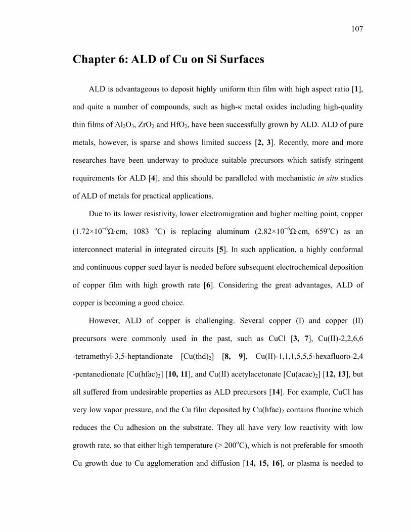
107
Chapter 6: ALD of Cu on Si Surfaces
ALD is advantageous to deposit highly uniform thin film with high aspect ratio [1],
and quite a number of compounds, such as high-κ metal oxides including high-quality
thin films of Al2O3, ZrO2 and HfO2, have been successfully grown by ALD. ALD of pure
metals, however, is sparse and shows limited success [2, 3]. Recently, more and more
researches have been underway to produce suitable precursors which satisfy stringent
requirements for ALD [4], and this should be paralleled with mechanistic in situ studies
of ALD of metals for practical applications.
Due to its lower resistivity, lower electromigration and higher melting point, copper
(1.72×10⁻⁶Ω·cm, 1083 oC) is replacing aluminum (2.82×10⁻⁶Ω·cm, 659oC) as an
interconnect material in integrated circuits [5]. In such application, a highly conformal
and continuous copper seed layer is needed before subsequent electrochemical deposition
of copper film with high growth rate [6]. Considering the great advantages, ALD of
copper is becoming a good choice.
However, ALD of copper is challenging. Several copper (I) and copper (II)
precursors were commonly used in the past, such as CuCl [3, 7], Cu(II)-2,2,6,6
-tetramethyl-3,5-heptandionate [Cu(thd)2] [8, 9], Cu(II)-1,1,1,5,5,5-hexafluoro-2,4
-pentanedionate [Cu(hfac)2] [10, 11], and Cu(II) acetylacetonate [Cu(acac)2] [12, 13], but
all suffered from undesirable properties as ALD precursors [14]. For example, CuCl has
very low vapor pressure, and the Cu film deposited by Cu(hfac)2 contains fluorine which
reduces the Cu adhesion on the substrate. They all have very low reactivity with low
growth rate, so that either high temperature (> 200oC), which is not preferable for smooth
Cu growth due to Cu agglomeration and diffusion [14, 15, 16], or plasma is needed to
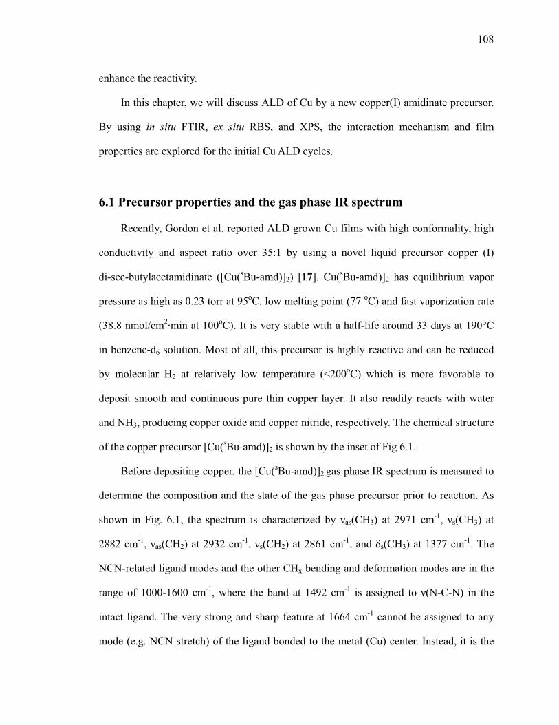
108
enhance the reactivity.
In this chapter, we will discuss ALD of Cu by a new copper(I) amidinate precursor.
By using in situ FTIR, ex situ RBS, and XPS, the interaction mechanism and film
properties are explored for the initial Cu ALD cycles.
6.1 Precursor properties and the gas phase IR spectrum
Recently, Gordon et al. reported ALD grown Cu films with high conformality, high
conductivity and aspect ratio over 35:1 by using a novel liquid precursor copper (I)
di-sec-butylacetamidinate ([Cu(sBu-amd)]2) [17]. Cu(sBu-amd)]2 has equilibrium vapor
pressure as high as 0.23 torr at 95oC, low melting point (77 oC) and fast vaporization rate
(38.8 nmol/cm2·min at 100oC). It is very stable with a half-life around 33 days at 190°C
in benzene-d6 solution. Most of all, this precursor is highly reactive and can be reduced
by molecular H2 at relatively low temperature (<200oC) which is more favorable to
deposit smooth and continuous pure thin copper layer. It also readily reacts with water
and NH3, producing copper oxide and copper nitride, respectively. The chemical structure
of the copper precursor [Cu(sBu-amd)]2 is shown by the inset of Fig 6.1.
Before depositing copper, the [Cu(sBu-amd)]2 gas phase IR spectrum is measured to
determine the composition and the state of the gas phase precursor prior to reaction. As
shown in Fig. 6.1, the spectrum is characterized by νas(CH3) at 2971 cm-1, νs(CH3) at
2882 cm-1, νas(CH2) at 2932 cm-1, νs(CH2) at 2861 cm-1, and δs(CH3) at 1377 cm-1. The
NCN-related ligand modes and the other CHx bending and deformation modes are in the
range of 1000-1600 cm-1, where the band at 1492 cm-1 is assigned to ν(N-C-N) in the
intact ligand. The very strong and sharp feature at 1664 cm-1 cannot be assigned to any
mode (e.g. NCN stretch) of the ligand bonded to the metal (Cu) center. Instead, it is the

109
characteristic of C=N stretching mode in the -HNC=N- molecule (HL, L denotes the
ligand) as the La precursor. Along with the ν(NH) at 3456 cm-1, the observed C=N
stretching mode at 1664 cm-1 is the result of partial hydrolization of the parent precursor,
most likely due to a small amount of residual water in the ALD chamber or precursor gas
line. This gas phase IR spectrum is useful to interpret some of the surface reactions.
For the following experiments, the precursor is kept at 94-100oC to generate a high
enough vapor pressure. During film deposition, the pressure of the copper precursor is
around 2 torr and that of H2/NH3 is >11 torr. The thickness of the ALD-grown copper
films is measured by ex situ RBS, assuming that the copper film density is equal to the
density of bulk copper (8.96 g/cm3, or 8.49×10²² atoms/cm3).
1000 1500 3000 3500
Fig 6.1 Gas phase FTIR absorption spectrum of the copper precursor [Cu(sBu-amd)]2
used in this study (Partial pressure ~0.4 torr , IR path length ~6 inch). Its chemical structure is shown on the upper left corner (inset).
6.2 ALD of Cu on H/Si surface
H/Si is the most widely used surface in microelectronics, and the Cu deposition is
first examined on H/Si surface. Fig. 6.2 shows the differential absorption spectra of
5×10⁻³
Wavenumbers (cm-1)
Abs
orba
nce
(a. u
.)
[Cu(sBu-amd)]2
ν (CHx)
ν (NH)
ν (C=N) 1664 cm-1
3456 cm-1
ν (NCN)
N N
Cu Cu
N N
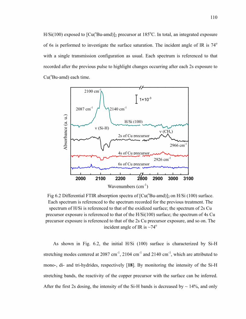
110
H/Si(100) exposed to [Cu(sBu-amd)]2 precursor at 185oC. In total, an integrated exposure
of 6s is performed to investigate the surface saturation. The incident angle of IR is 74o
with a single transmission configuration as usual. Each spectrum is referenced to that
recorded after the previous pulse to highlight changes occurring after each 2s exposure to
Cu(sBu-amd) each time.
2000 2100 2200 2800 2900 3000 3100
Fig 6.2 Differential FTIR absorption spectra of [Cu(sBu-amd)]2 on H/Si (100) surface. Each spectrum is referenced to the spectrum recorded for the previous treatment. The spectrum of H/Si is referenced to that of the oxidized surface; the spectrum of 2s Cu
precursor exposure is referenced to that of the H/Si(100) surface; the spectrum of 4s Cu precursor exposure is referenced to that of the 2s Cu precursor exposure, and so on. The
incident angle of IR is ~74o
As shown in Fig. 6.2, the initial H/Si (100) surface is characterized by Si-H
stretching modes centered at 2087 cm-1, 2104 cm-1 and 2140 cm-1, which are attributed to
mono-, di- and tri-hydrides, respectively [18]. By monitoring the intensity of the Si-H
stretching bands, the reactivity of the copper precursor with the surface can be inferred.
After the first 2s dosing, the intensity of the Si-H bands is decreased by ~ 14%, and only
Wavenumbers (cm-1)
Abs
orba
nce
(a. u
.)
ν (CHx) ν (Si-H)
1×10⁻³
H/Si (100)
2s of Cu precursor
4s of Cu precursor
6s of Cu precursor2926 cm-1
2966 cm-1
2087 cm-1
2100 cm-1
2140 cm-1
111
by ~ 21% and ~22% (relative to the original H/Si surface) after the second (4s) and third
exposures (6s), respectively. The change after 4s exposure is negligible according to the
differential spectra, suggesting no more chemical bonding formation. These data indicate
that the saturation is achieved after ~ 4s integrated exposure time. Concurrently, the
asymmetric stretching modes of CH3 at 2966 cm-1 and CH2 2926 cm-1 are observed after
the first dosing of Cu precursor with little intensity increase afterwards. The behavior of
Si-H and CHx stretching modes indicates that most of the surface reaction occurs during
the first precursor dosing (2-4s exposure). RBS measurement performed after 2 cycles of
[Cu(sBu-amd)]2/H2 on H/Si(100) shows that the Cu thickness is about 0.24 Å.
2050 2100 2150
5x10⁻⁴
Fig 6.3(a) Absorption spectra of 10 cycles Cu on H/Si(111) reference to oxide (left) and (b) the plot of the loss of Si-H vs number cycles (right). The incident angle of IR is ~74o.
The Cu precursor can react with H/Si.
A study has shown that there is no Cu growth on H/Si surface by this precursor [14]
but our spectra clearly show that there are obvious chemical reactions between
[Cu(sBu-amd)]2 and H/Si. To confirm it, atomically flat and almost defect-free
0 2 4 6 8 10 12
0.0
0.5
1.0
Number of cycles
(b)
Wavenumbers (cm-1)
Abs
orba
nce
(a. u
.)
2083 cm-1
Loss
of S
i-H
H/Si(111)
1cyc
2cyc
3cyc
5cyc 10cyc
Si-H
(a)
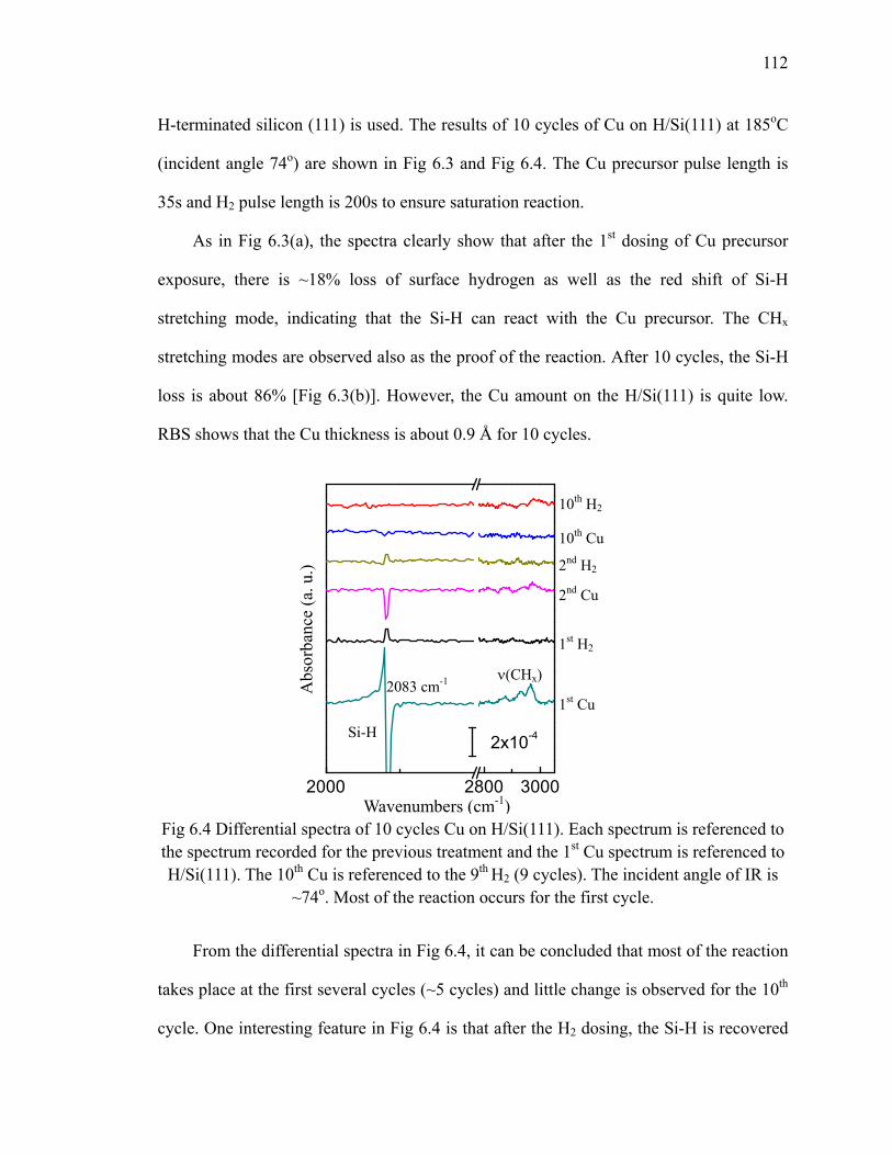
112
H-terminated silicon (111) is used. The results of 10 cycles of Cu on H/Si(111) at 185oC
(incident angle 74o) are shown in Fig 6.3 and Fig 6.4. The Cu precursor pulse length is
35s and H2 pulse length is 200s to ensure saturation reaction.
As in Fig 6.3(a), the spectra clearly show that after the 1st dosing of Cu precursor
exposure, there is ~18% loss of surface hydrogen as well as the red shift of Si-H
stretching mode, indicating that the Si-H can react with the Cu precursor. The CHx
stretching modes are observed also as the proof of the reaction. After 10 cycles, the Si-H
loss is about 86% [Fig 6.3(b)]. However, the Cu amount on the H/Si(111) is quite low.
RBS shows that the Cu thickness is about 0.9 Å for 10 cycles.
2000 2800 3000
2x10⁻⁴
Fig 6.4 Differential spectra of 10 cycles Cu on H/Si(111). Each spectrum is referenced to the spectrum recorded for the previous treatment and the 1st Cu spectrum is referenced to H/Si(111). The 10th Cu is referenced to the 9th H2 (9 cycles). The incident angle of IR is
~74o. Most of the reaction occurs for the first cycle.
From the differential spectra in Fig 6.4, it can be concluded that most of the reaction
takes place at the first several cycles (~5 cycles) and little change is observed for the 10th
cycle. One interesting feature in Fig 6.4 is that after the H2 dosing, the Si-H is recovered
Wavenumbers (cm-1)
Abs
orba
nce
(a. u
.)
10th Cu
10th H2
2nd H2
2nd Cu
1st H2
1st Cu 2083 cm-1
Si-H
ν(CHx)

113
partially. It may result from the Cu diffusion into Si by forming CuSi3 [19, 20, 21], where
H2 reduces the Cu precursor attached on the Si surface to Cu atoms and a few Cu atoms
diffuse into the Si network to free the surface Si atoms, which are passivated again by H.
6.3 ALD of Cu on SiO2
In general, oxidized Si surface is much more reactive to metal precursors than H/Si
surface. We therefore studied the reactivity of [Cu(sBu-amd)]2 with Si(100) covered by
thin oxide (60-100 Å). On this surface, Cu is deposited at different temperatures, with 35s
dosing of [Cu(sBu-amd)]2 and 200s dosing of H2 to study the temperature dependence of
ALD.
Deposition at 185oC
The differential absorption spectra for the first 3 cycles Cu deposited on SiO2 at
185oC are shown in Fig 6.5, where each spectrum is referenced to that of the previous
treatment to see the change on the surface after each treatment.
As shown in the spectra, upon the initial dosing of [Cu(sBu-amd)]2 on the oxide
surface, there is a clear intensity decrease of SiOx phonon absorption evidenced by two
negative peaks centered at 1075 cm-1 and 1247 cm-1 (TO/LO modes of Si-O-Si), along
with the loss of isolated -OH stretching/bending modes at 3737 cm-1 and 1660 cm-1
respectively [22]. Their intensity loss indicates that initially a part of the SiO2 matrix is
chemically involved with the Cu precursor. Concurrently, a broad absorption band
centered at 1010 cm-1 appears, corresponded to the formation of Si-O-Cu bonds due to
the adsorbed Cu precursor on SiO2. The reaction scheme is shown in Fig 6.6(a) and (b).
Upon the H2 exposure (1 cycle), there is a partial recovery of SiOx phonon modes and
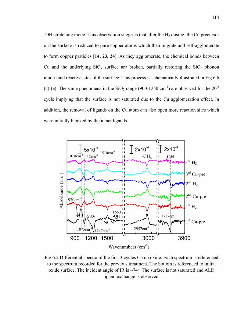
114
-OH stretching mode. This observation suggests that after the H2 dosing, the Cu precursor
on the surface is reduced to pure copper atoms which then migrate and self-agglomerate
to form copper particles [14, 23, 24]. As they agglomerate, the chemical bonds between
Cu and the underlying SiOx surface are broken, partially restoring the SiO2 phonon
modes and reactive sites of the surface. This process is schematically illustrated in Fig 6.6
(c)-(e). The same phenomena in the SiO2 range (900-1250 cm-1) are observed for the 20th
cycle implying that the surface is not saturated due to the Cu agglomeration effect. In
addition, the removal of ligands on the Cu atom can also open more reaction sites which
were initially blocked by the intact ligands.
Fig 6.5 Differential spectra of the first 3 cycles Cu on oxide. Each spectrum is referenced
to the spectrum recorded for the previous treatment. The bottom is referenced to initial oxide surface. The incident angle of IR is ~74o. The surface is not saturated and ALD
ligand exchange is observed.
900 1200 1500
5x10⁻⁴
3000
2x10⁻⁴
3900
2x10⁻⁴
1st Cu-pre
1st H2
2nd Cu-pre
2nd H2
3rd H2
3rd Cu-pre
1010cm-1
1075cm-1
-CHx1510cm-1
3737cm-1
-OH
1247cm-1
-NCN-
Wavenumbers (cm-1)
Abs
orba
nce
(a. u
.)
1112cm-1
2957cm-1
970cm-1
1660-OH SiO2
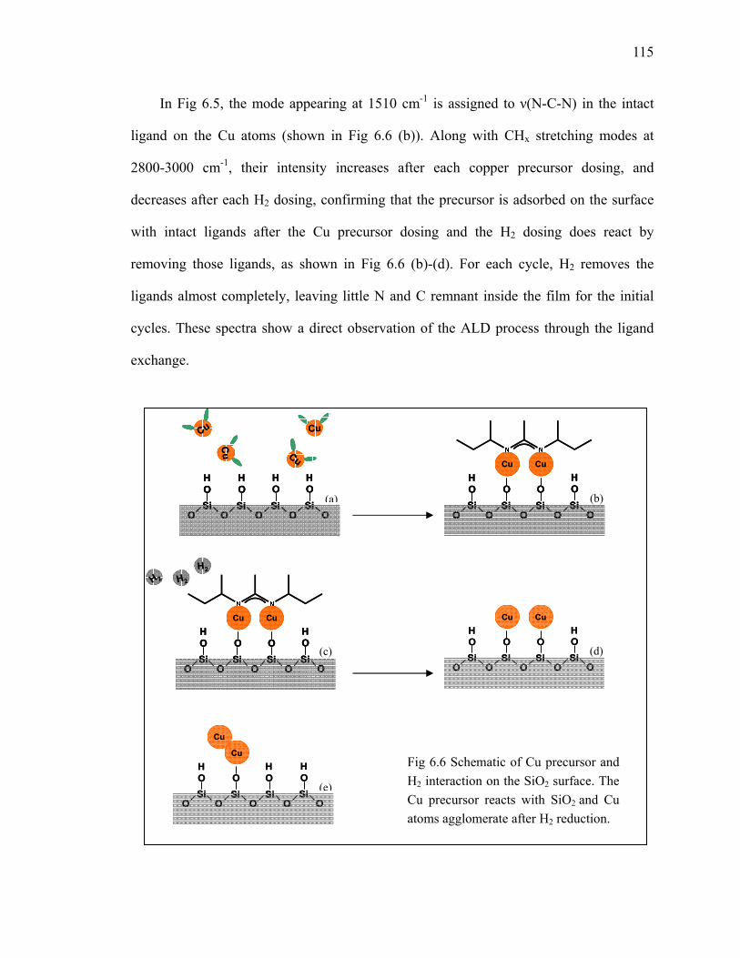
115
In Fig 6.5, the mode appearing at 1510 cm-1 is assigned to ν(N-C-N) in the intact
ligand on the Cu atoms (shown in Fig 6.6 (b)). Along with CHx stretching modes at
2800-3000 cm-1, their intensity increases after each copper precursor dosing, and
decreases after each H2 dosing, confirming that the precursor is adsorbed on the surface
with intact ligands after the Cu precursor dosing and the H2 dosing does react by
removing those ligands, as shown in Fig 6.6 (b)-(d). For each cycle, H2 removes the
ligands almost completely, leaving little N and C remnant inside the film for the initial
cycles. These spectra show a direct observation of the ALD process through the ligand
exchange.
SiO
HO
OSi
OSi
OSi
O
OHOO
Cu Cu
SiO
HO
OSi
OSi
OSi
O
OHOO
Cu Cu
SiO
HO
OSi
OSi
OSi
O
OHOO
Cu Cu
(b)
(c)Si
O
HO
OSi
OSi
OSi
O
OHOO
Cu Cu
H 2 H2
H2
SiO
HO
OSi
OSi
OSi
O
OHOO
Cu Cu
SiO
HO
OSi
OSi
OSi
O
OHOO
Cu Cu
H 2 H2
H2
SiO
HO
OSi
OSi
OSi
O
OHOO
Cu Cu
SiO
HO
OSi
OSi
OSi
O
OHOO
Cu Cu
(d)
SiO
HO
OSi
OSi
OSi
O
OHO
Cu
Cu
HO
SiO
HO
OSi
OSi
OSi
O
OHO
Cu
Cu
HO
(e)
SiO
HO
OSi
OSi
OSi
O
HO
HO
HO
Cu
Cu Cu
Cu
SiO
HO
OSi
OSi
OSi
O
HO
HO
HO
SiO
HO
OSi
OSi
OSi
O
HO
HO
HO
CuCu
Cu
Cu CuCu
CuCu
(a)
Fig 6.6 Schematic of Cu precursor and H2 interaction on the SiO2 surface. The Cu precursor reacts with SiO2 and Cu atoms agglomerate after H2 reduction.

116
The spectra of subsequent cycles (up to 20 cycles) referenced to the initial SiO2
surface are presented in Fig 6.7 to show the Cu film on SiO2. Two incident angles are
used, ~74o (left) and ~0o (right), to see the polarization effect. IR of 74o incidence is
sensitive to both parallel and perpendicular components to the surface, while normal
incidence is only sensitive to the parallel component. The spectra show that there is no
difference between the two angles, indicating that the film is isotropic. Consequently, the
strong peaks at 1010 cm-1 and 1112 cm-1 cannot be assigned to SiO2 TO/LO modes since
the LO mode of SiO2 is angle dependent and will not appear at normal incidence. Their
frequencies are also much lower than that of typical SiO2 TO/LO modes which are
around 1075 cm-1 and 1247 cm-1 respectively as observed in Fig 6.5.
900 1200 1500 3000
3x10⁻³
900 1200 1500 3000
3x10⁻³
Fig 6.7 Absorption spectra of the first 3 cycles Cu on Si oxide. Each spectrum is
referenced to the spectrum recorded for the previous treatment. The bottom one is referenced to initial oxide surface. The left one is taken at 74o and the right one is taken at
0o. Ligand related impurities are observed and spectra show little difference at different angles.
It is most likely that they are related to Cu-incorporated Si oxide as Cu-SiOx modes
[25, 26, 27] because Cu-O stretching modes are all below 700 cm-1 [28, 29, 30]. By peak
Wavenumbers (cm-1)
Abs
orba
nce
(a. u
.)
74o 0o
1010cm-1
1112cm-1 1112cm-1
1010cm-1
10cyc5cyc1cyc
20cyc
C,H,NCHx CHx C,H,N
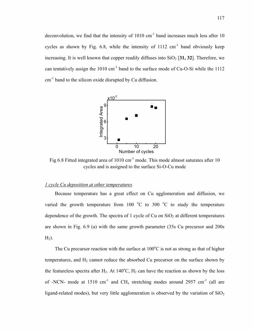
117
deconvolution, we find that the intensity of 1010 cm-1 band increases much less after 10
cycles as shown by Fig. 6.8, while the intensity of 1112 cm-1 band obviously keep
increasing. It is well known that copper readily diffuses into SiO2 [31, 32]. Therefore, we
can tentatively assign the 1010 cm-1 band to the surface mode of Cu-O-Si while the 1112
cm-1 band to the silicon oxide disrupted by Cu diffusion.
0 10 20
3
6
9
Inte
grat
ed A
rea
Number of cycles
x10-2
Fig 6.8 Fitted integrated area of 1010 cm-1 mode. This mode almost saturates after 10
cycles and is assigned to the surface Si-O-Cu mode
1 cycle Cu deposition at other temperatures
Because temperature has a great effect on Cu agglomeration and diffusion, we
varied the growth temperature from 100 oC to 300 oC to study the temperature
dependence of the growth. The spectra of 1 cycle of Cu on SiO2 at different temperatures
are shown in Fig. 6.9 (a) with the same growth parameter (35s Cu precursor and 200s
H2).
The Cu precursor reaction with the surface at 100oC is not as strong as that of higher
temperatures, and H2 cannot reduce the absorbed Cu precursor on the surface shown by
the featureless spectra after H2. At 140oC, H2 can have the reaction as shown by the loss
of -NCN- mode at 1510 cm-1 and CHx stretching modes around 2957 cm-1 (all are
ligand-related modes), but very little agglomeration is observed by the variation of SiO2
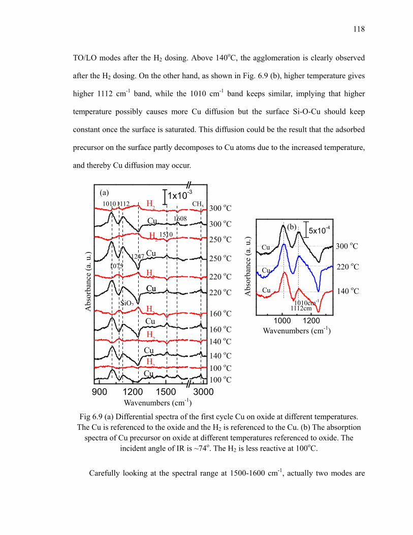
118
TO/LO modes after the H2 dosing. Above 140oC, the agglomeration is clearly observed
after the H2 dosing. On the other hand, as shown in Fig. 6.9 (b), higher temperature gives
higher 1112 cm-1 band, while the 1010 cm-1 band keeps similar, implying that higher
temperature possibly causes more Cu diffusion but the surface Si-O-Cu should keep
constant once the surface is saturated. This diffusion could be the result that the adsorbed
precursor on the surface partly decomposes to Cu atoms due to the increased temperature,
and thereby Cu diffusion may occur.
Fig 6.9 (a) Differential spectra of the first cycle Cu on oxide at different temperatures.
The Cu is referenced to the oxide and the H2 is referenced to the Cu. (b) The absorption spectra of Cu precursor on oxide at different temperatures referenced to oxide. The
incident angle of IR is ~74o. The H2 is less reactive at 100oC.
Carefully looking at the spectral range at 1500-1600 cm-1, actually two modes are
900 1200 1500 3000
1x10⁻³
Cu
Cu
Cu
Cu
Cu
H2
H2
H2
H2
H2
Cu
CuH2
1010cm-1
(a)
(b)
Wavenumbers (cm-1)
Abs
orba
nce
(a. u
.)
300 oC
300 oC
220 oC
220 oC
160 oC
160 oC140 oC
140 oC100 oC100 oC
1000 1200
Cu
Cu
5x10⁻⁴
Cu
Wavenumbers (cm-1)
Abs
orba
nce
(a. u
.)
1112cm
300 oC
220 oC
140 oC
250 oC
250 oC
1112 1010
1075 1247
1510
1608
CHx
SiO2
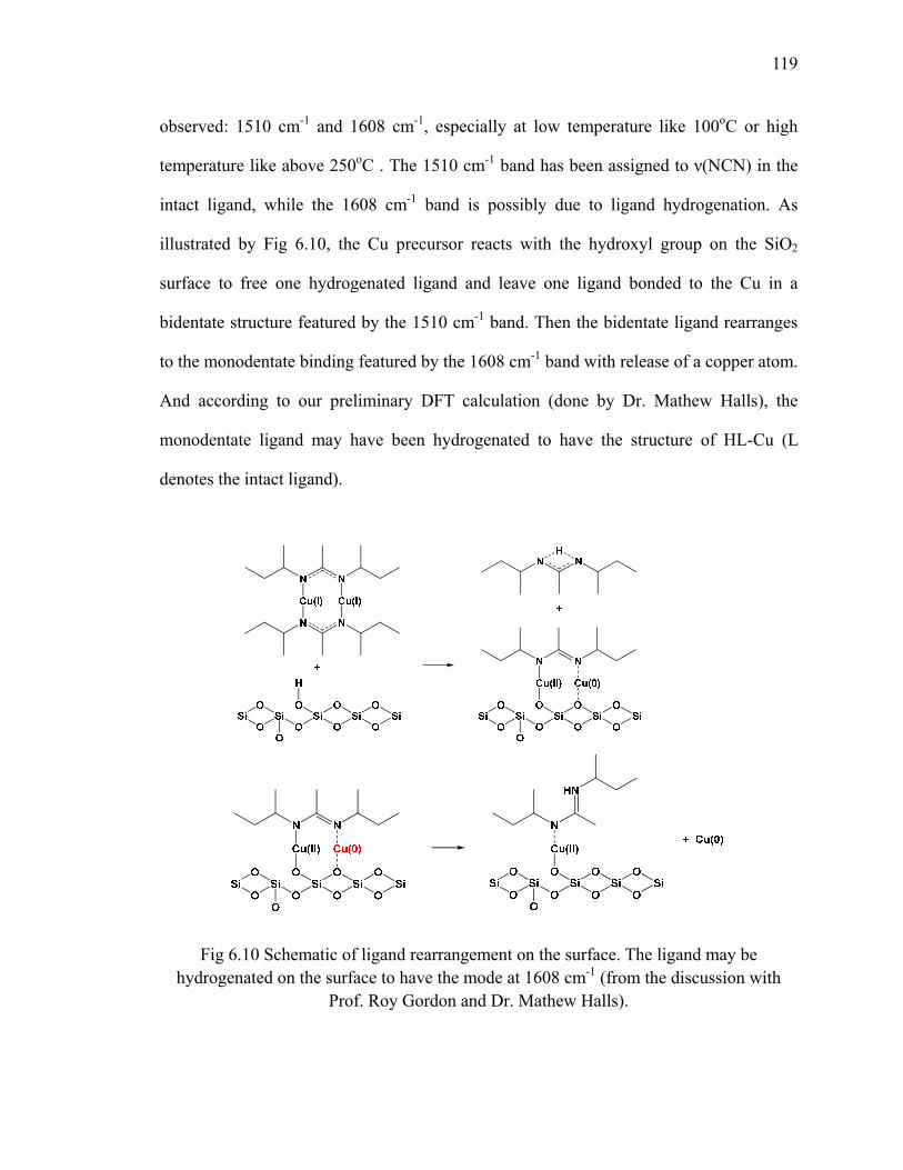
119
observed: 1510 cm-1 and 1608 cm-1, especially at low temperature like 100oC or high
temperature like above 250oC . The 1510 cm-1 band has been assigned to ν(NCN) in the
intact ligand, while the 1608 cm-1 band is possibly due to ligand hydrogenation. As
illustrated by Fig 6.10, the Cu precursor reacts with the hydroxyl group on the SiO2
surface to free one hydrogenated ligand and leave one ligand bonded to the Cu in a
bidentate structure featured by the 1510 cm-1 band. Then the bidentate ligand rearranges
to the monodentate binding featured by the 1608 cm-1 band with release of a copper atom.
And according to our preliminary DFT calculation (done by Dr. Mathew Halls), the
monodentate ligand may have been hydrogenated to have the structure of HL-Cu (L
denotes the intact ligand).
Fig 6.10 Schematic of ligand rearrangement on the surface. The ligand may be
hydrogenated on the surface to have the mode at 1608 cm-1 (from the discussion with Prof. Roy Gordon and Dr. Mathew Halls).
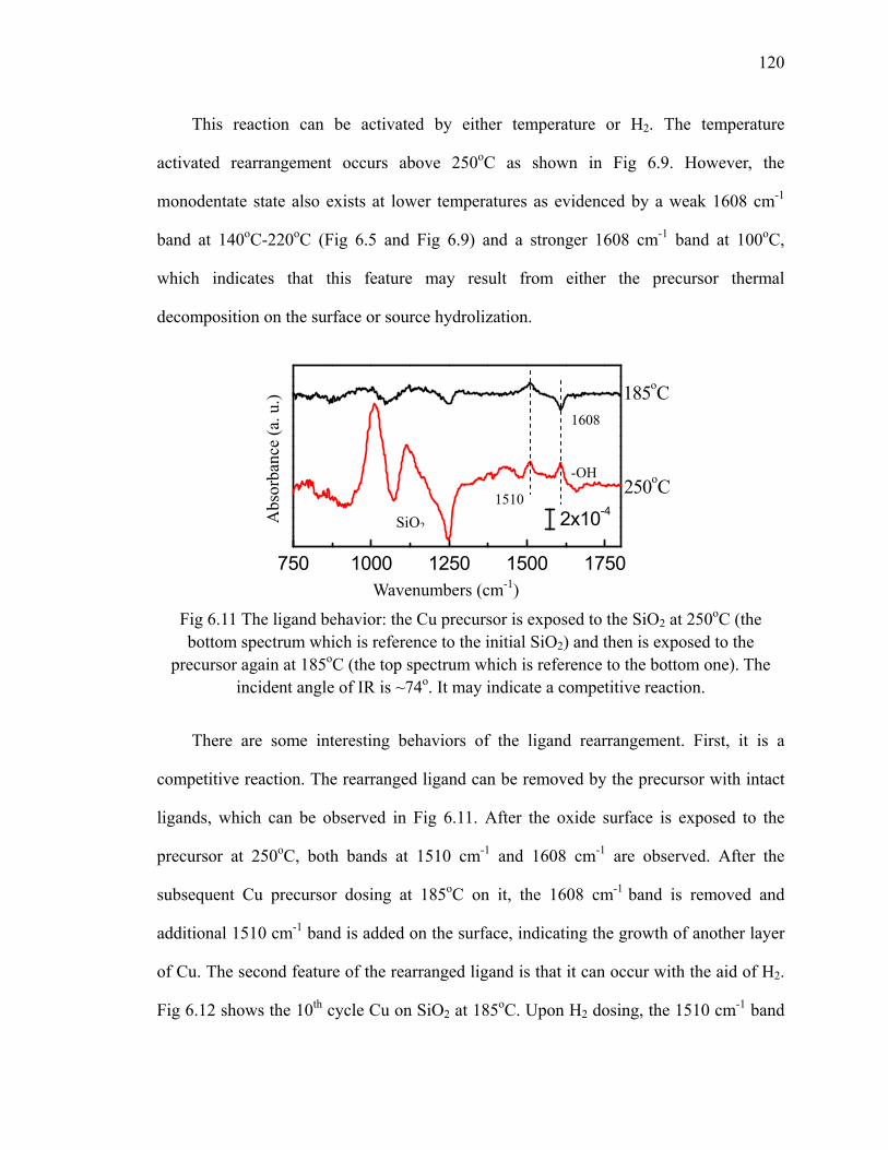
120
This reaction can be activated by either temperature or H2. The temperature
activated rearrangement occurs above 250oC as shown in Fig 6.9. However, the
monodentate state also exists at lower temperatures as evidenced by a weak 1608 cm-1
band at 140oC-220oC (Fig 6.5 and Fig 6.9) and a stronger 1608 cm-1 band at 100oC,
which indicates that this feature may result from either the precursor thermal
decomposition on the surface or source hydrolization.
Fig 6.11 The ligand behavior: the Cu precursor is exposed to the SiO2 at 250oC (the bottom spectrum which is reference to the initial SiO2) and then is exposed to the
precursor again at 185oC (the top spectrum which is reference to the bottom one). The incident angle of IR is ~74o. It may indicate a competitive reaction.
There are some interesting behaviors of the ligand rearrangement. First, it is a
competitive reaction. The rearranged ligand can be removed by the precursor with intact
ligands, which can be observed in Fig 6.11. After the oxide surface is exposed to the
precursor at 250oC, both bands at 1510 cm-1 and 1608 cm-1 are observed. After the
subsequent Cu precursor dosing at 185oC on it, the 1608 cm-1 band is removed and
additional 1510 cm-1 band is added on the surface, indicating the growth of another layer
of Cu. The second feature of the rearranged ligand is that it can occur with the aid of H2.
Fig 6.12 shows the 10th cycle Cu on SiO2 at 185oC. Upon H2 dosing, the 1510 cm-1 band
750 1000 1250 1500 1750
185oC
2x10⁻⁴
250oC
Wavenumbers (cm-1)
Abs
orba
nce
(a. u
.)
1510
1608
-OH
SiO2

121
is removed and the 1608 cm-1 band appears, implying that a part of the bidentate ligands
are rearranged to the hydrogenated monodentate state (HL). At 300oC, both intact
(bidentate) and rearranged (monodentate) ligands are removed by H2 as shown in Fig
6.9(a).
900 1200 1500 3000
10th H2
1x10-4185oC
10th Cu
Fig 6.12 The differential spectra of the 10th cycle of Cu deposited on SiO2 at 185oC: the 10th Cu spectrum is reference to the 9 cycles (9th H2) and the 10th H2 is reference to the
10th Cu. The incident angle of IR is ~74o.
Note that another mode at 970 cm-1 appears simultaneously with 1112 cm-1 after the
10th Cu precursor dosing (see Fig. 6.12), and it can be possibly assigned to another mode
of Cu in SiO2 [25]. It has no polarization dependence according to the IR
angle-dependence study. This mode appears as a shoulder after the 1st Cu precursor
dosing as shown in Fig 6.5 and 6.9 but not at 100oC, confirming its assignment.
Considering the ligand rearrangement and H2 reactivity, the appropriate temperature
range for the Cu deposition is between 140oC and 220oC; i.e., monodentate state of
hydrogenated ligand at 1608 cm-1 is minimal after the Cu precursor dosing and the
reactivity of H2 is high enough.
Cu deposition at 140oC and 125oC
As shown in Fig 6.9, less Cu agglomeration and diffusion is observed below 140 oC
1510
1608
970 1112
Wavenumbers (cm-1)
Abs
orba
nce
(a. u
.)
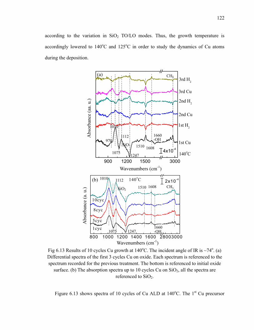
122
according to the variation in SiO2 TO/LO modes. Thus, the growth temperature is
accordingly lowered to 140oC and 125oC in order to study the dynamics of Cu atoms
during the deposition.
Fig 6.13 Results of 10 cycles Cu growth at 140oC. The incident angle of IR is ~74o. (a) Differential spectra of the first 3 cycles Cu on oxide. Each spectrum is referenced to the spectrum recorded for the previous treatment. The bottom is referenced to initial oxide
surface. (b) The absorption spectra up to 10 cycles Cu on SiO2, all the spectra are referenced to SiO2.
Figure 6.13 shows spectra of 10 cycles of Cu ALD at 140oC. The 1st Cu precursor
800 1000 1200 1400 1600 28003000
1cyc
8cyc
5cyc
2x10⁻⁴
10cyc
140oC
Wavenumbers (cm-1)
Abs
orba
nce
(a. u
.) CHx 1112 1010
1075 1247
1510 1608
1660-OH
900 1200 1500 3000
1st H2
4x10⁻⁴
1st Cu
2nd H2
2nd Cu
3rd H2
3rd Cu
140oC
Wavenumbers (cm-1)
Abs
orba
nce
(aa.
u.)
CHx
1112
1010
1075 1247
1510 1608
1660-OH 970
(a)
(b)
SiO2
SiO2
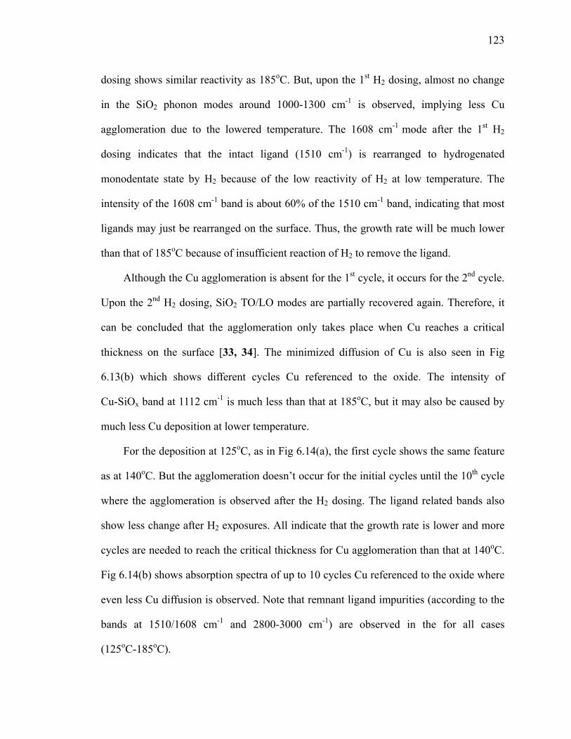
123
dosing shows similar reactivity as 185oC. But, upon the 1st H2 dosing, almost no change
in the SiO2 phonon modes around 1000-1300 cm-1 is observed, implying less Cu
agglomeration due to the lowered temperature. The 1608 cm-1 mode after the 1st H2
dosing indicates that the intact ligand (1510 cm-1) is rearranged to hydrogenated
monodentate state by H2 because of the low reactivity of H2 at low temperature. The
intensity of the 1608 cm-1 band is about 60% of the 1510 cm-1 band, indicating that most
ligands may just be rearranged on the surface. Thus, the growth rate will be much lower
than that of 185oC because of insufficient reaction of H2 to remove the ligand.
Although the Cu agglomeration is absent for the 1st cycle, it occurs for the 2nd cycle.
Upon the 2nd H2 dosing, SiO2 TO/LO modes are partially recovered again. Therefore, it
can be concluded that the agglomeration only takes place when Cu reaches a critical
thickness on the surface [33, 34]. The minimized diffusion of Cu is also seen in Fig
6.13(b) which shows different cycles Cu referenced to the oxide. The intensity of
Cu-SiOx band at 1112 cm-1 is much less than that at 185oC, but it may also be caused by
much less Cu deposition at lower temperature.
For the deposition at 125oC, as in Fig 6.14(a), the first cycle shows the same feature
as at 140oC. But the agglomeration doesn’t occur for the initial cycles until the 10th cycle
where the agglomeration is observed after the H2 dosing. The ligand related bands also
show less change after H2 exposures. All indicate that the growth rate is lower and more
cycles are needed to reach the critical thickness for Cu agglomeration than that at 140oC.
Fig 6.14(b) shows absorption spectra of up to 10 cycles Cu referenced to the oxide where
even less Cu diffusion is observed. Note that remnant ligand impurities (according to the
bands at 1510/1608 cm-1 and 2800-3000 cm-1) are observed in the for all cases
(125oC-185oC).

124
Fig 6.14 Results of 10 cycles Cu growth at 125oC. The incident angle of IR is ~74o. (a) Differential spectra of the first 2 cycles Cu and 10th cycle on oxide. Each spectrum is
referenced to the spectrum recorded for the previous treatment. The bottom is referenced to initial oxide surface and the 10th Cu is referenced to 9 cycles (9th H2). (b) The
absorption spectra up to 10 cycles Cu on SiO2, all the spectra are referenced to SiO2.
RBS and XPS analysis of Cu on SiO2
The areal density of Cu atoms is measured by ex situ RBS. Table 6.1 shows the RBS
results of 10 ALD cycles of Cu on SiO2 at 125oC, 140oC, and 185oC with the accuracy
900 1200 1500 3000
125oC
10cyc
5cyc
2cyc
4x10⁻⁴
1cyc
1112 1010
1075 1247
1608 970
1660-OH
CHx
Wavenumbers (cm-1)
Abs
orba
nce
(a. u
.)
(b)
1510
900 1200 1500 3000
1st H2
2x10⁻⁴
1st Cu
2nd H2
2nd Cu
10th H2
10th Cu
125oC
1112
1010
1075 1247
1510 1608
970 1660-OH
CHx
Wavenumbers (cm-1)
Abs
orba
nce
(a. u
.)
(a)
SiO2
SiO2
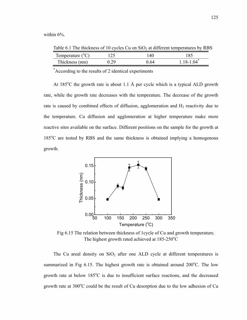
125
within 6%.
Table 6.1 The thickness of 10 cycles Cu on SiO2 at different temperatures by RBS Temperature (oC) 125 140 185 Thickness (nm) 0.29 0.64 1.18-1.04*
*According to the results of 2 identical experiments
At 185oC the growth rate is about 1.1 Å per cycle which is a typical ALD growth
rate, while the growth rate decreases with the temperature. The decrease of the growth
rate is caused by combined effects of diffusion, agglomeration and H2 reactivity due to
the temperature. Cu diffusion and agglomeration at higher temperature make more
reactive sites available on the surface. Different positions on the sample for the growth at
185oC are tested by RBS and the same thickness is obtained implying a homogenous
growth.
50 100 150 200 250 300 3500.00
0.05
0.10
0.15
Temperature (oC)
Thic
knes
s (n
m)
Fig 6.15 The relation between thickness of 1cycle of Cu and growth temperature.
The highest growth rated achieved at 185-250oC
The Cu areal density on SiO2 after one ALD cycle at different temperatures is
summarized in Fig 6.15. The highest growth rate is obtained around 200oC. The low
growth rate at below 185oC is due to insufficient surface reactions, and the decreased
growth rate at 300oC could be the result of Cu desorption due to the low adhesion of Cu
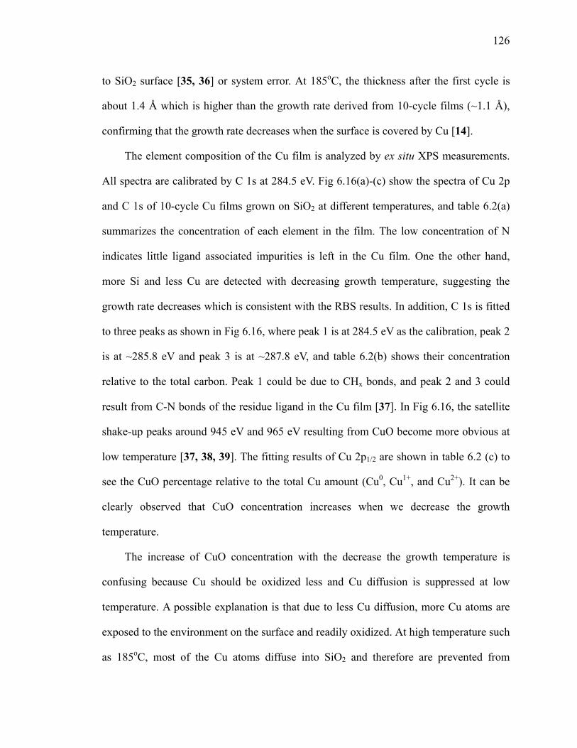
126
to SiO2 surface [35, 36] or system error. At 185oC, the thickness after the first cycle is
about 1.4 Å which is higher than the growth rate derived from 10-cycle films (~1.1 Å),
confirming that the growth rate decreases when the surface is covered by Cu [14].
The element composition of the Cu film is analyzed by ex situ XPS measurements.
All spectra are calibrated by C 1s at 284.5 eV. Fig 6.16(a)-(c) show the spectra of Cu 2p
and C 1s of 10-cycle Cu films grown on SiO2 at different temperatures, and table 6.2(a)
summarizes the concentration of each element in the film. The low concentration of N
indicates little ligand associated impurities is left in the Cu film. One the other hand,
more Si and less Cu are detected with decreasing growth temperature, suggesting the
growth rate decreases which is consistent with the RBS results. In addition, C 1s is fitted
to three peaks as shown in Fig 6.16, where peak 1 is at 284.5 eV as the calibration, peak 2
is at ~285.8 eV and peak 3 is at ~287.8 eV, and table 6.2(b) shows their concentration
relative to the total carbon. Peak 1 could be due to CHx bonds, and peak 2 and 3 could
result from C-N bonds of the residue ligand in the Cu film [37]. In Fig 6.16, the satellite
shake-up peaks around 945 eV and 965 eV resulting from CuO become more obvious at
low temperature [37, 38, 39]. The fitting results of Cu 2p1/2 are shown in table 6.2 (c) to
see the CuO percentage relative to the total Cu amount (Cu0, Cu1+, and Cu2+). It can be
clearly observed that CuO concentration increases when we decrease the growth
temperature.
The increase of CuO concentration with the decrease the growth temperature is
confusing because Cu should be oxidized less and Cu diffusion is suppressed at low
temperature. A possible explanation is that due to less Cu diffusion, more Cu atoms are
exposed to the environment on the surface and readily oxidized. At high temperature such
as 185oC, most of the Cu atoms diffuse into SiO2 and therefore are prevented from
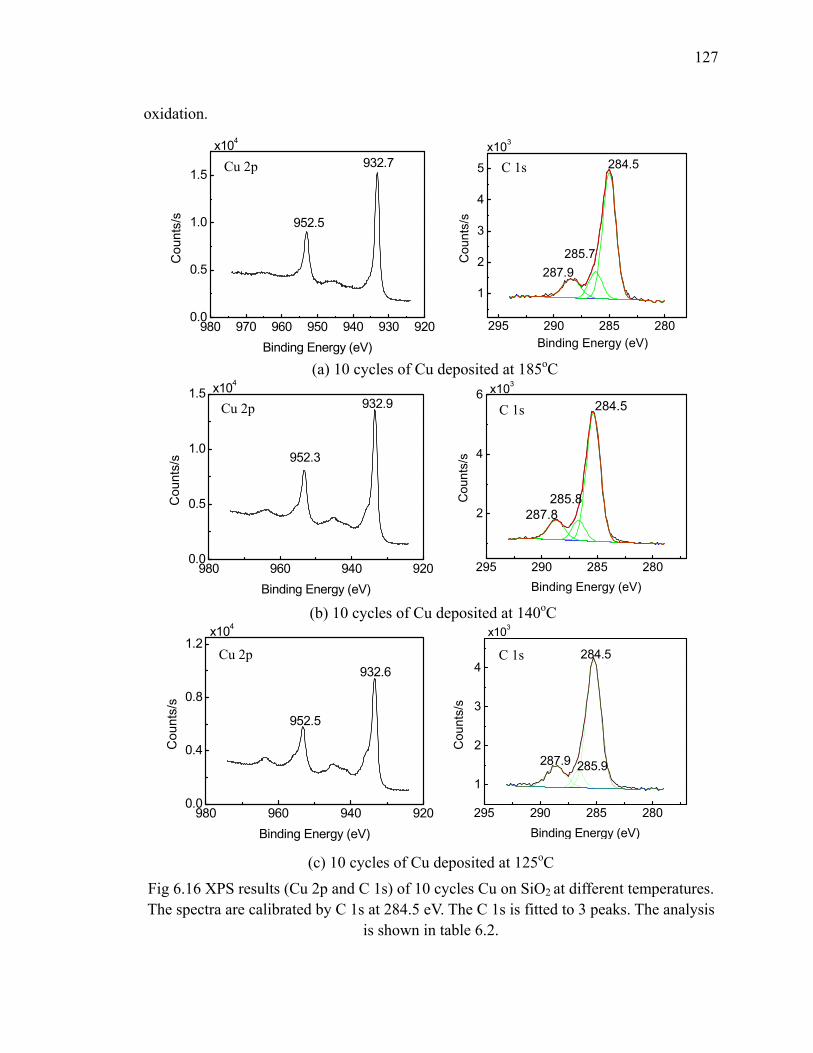
127
oxidation.
(c) 10 cycles of Cu deposited at 125oC Fig 6.16 XPS results (Cu 2p and C 1s) of 10 cycles Cu on SiO2 at different temperatures. The spectra are calibrated by C 1s at 284.5 eV. The C 1s is fitted to 3 peaks. The analysis
is shown in table 6.2.
295 290 285 280
1
2
3
4
287.9 285.9
Cou
nts/
s
Binding Energy (eV)
x103
284.5
980 960 940 9200.0
0.4
0.8
1.2
Cou
nts/
s
Binding Energy (eV)
x104
932.6
952.5
Cu 2p C 1s
980 970 960 950 940 930 9200.0
0.5
1.0
1.5
952.5
Cou
nts/
s
Binding Energy (eV)
x104
932.7
295 290 285 280
1
2
3
4
5
287.9
Cou
nts/
s
Binding Energy (eV)
x103
284.5
285.7
Cu 2p C 1s
(a) 10 cycles of Cu deposited at 185oC
295 290 285 280
2
4
6
287.8285.8
Cou
nts/
s
Binding Energy (eV)
x103
284.5
980 960 940 9200.0
0.5
1.0
1.5932.9
Cou
nts/
s
Binding Energy (eV)
x104
952.3
Cu 2p C 1s
(b) 10 cycles of Cu deposited at 140oC

128
Table 6.2(a) The summary of element concentration by XPS results for 10 cycles of Cu on SiO2 at different temperatures.
Elements Cu C N O Si 185oC 17.8 47.6 1.8 26.8 6.0 140oC 13.5 37.8 1.3 35.2 12.2
Concentration (%)
125oC 11.2 30.1 0.9 41.8 16.0
Table 6.2 (b) The concentration of different carbons in total C for three fitted C 1s peaks for 10 cycles of Cu on SiO2 at different temperatures.(Peak 1 ~284.5 eV, Peak 2 ~285.8
eV, and Peak 3 ~287.8 eV) .C 1s (eV) Peak 1 Peak 2 Peak 3
185oC 70.7 15.0 14.3 140oC 75.4 10.9 13.7
Concentration in C (%)
125oC 76.0 7.5 16.5
Table 6.2 (c) The relative CuO concentration in total Cu
Temperature 185oC 140oC 125oC CuO (%) in Cu 13% ± 2% 20% ± 5% 26% ± 5%
Fig 6.17 XPS results (Cu 2p and C 1s) of 10 cycles Cu on SiO2 at 140oC (fresh sample
transferred to XPS chamber immediately). The spectra are calibrated by C 1s at 284.5 eV. The amount of CuO and C impurities is reduced. Table 6.3 shows the analysis summary.
Table 6.3(a) The summary of element concentration by XPS results for 10 cycles of Cu on SiO2 at 140oC (fresh sample transferred to XPS chamber immediately).
Elements Cu C N O Si Concentration (%) 20.1 26.3 1.6 38.2 13.8
980 970 960 950 940 930 9200.0
0.8
1.6
2.4
Cou
nts/
s
Binding Energy (eV)
x104
932.6
952.5
295 290 285 280
1
2
3
4
287.8
284.5
Cou
nts/
s
Binding Energy (eV)
x103
286.0
Cu 2p C 1s
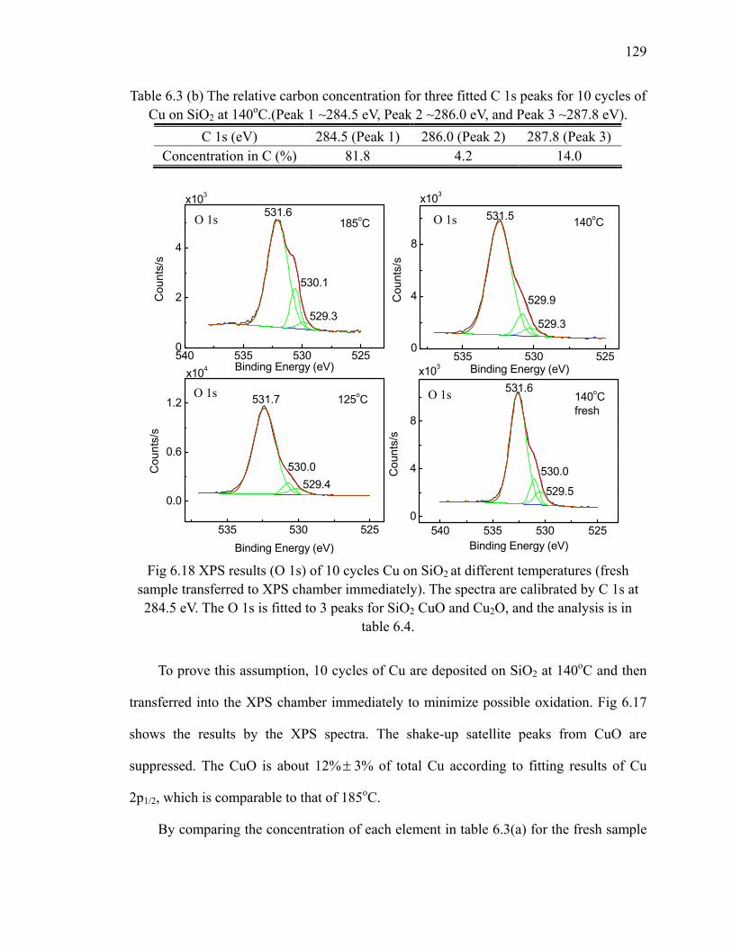
129
Table 6.3 (b) The relative carbon concentration for three fitted C 1s peaks for 10 cycles of Cu on SiO2 at 140oC.(Peak 1 ~284.5 eV, Peak 2 ~286.0 eV, and Peak 3 ~287.8 eV).
C 1s (eV) 284.5 (Peak 1) 286.0 (Peak 2) 287.8 (Peak 3) Concentration in C (%) 81.8 4.2 14.0
Fig 6.18 XPS results (O 1s) of 10 cycles Cu on SiO2 at different temperatures (fresh sample transferred to XPS chamber immediately). The spectra are calibrated by C 1s at 284.5 eV. The O 1s is fitted to 3 peaks for SiO2 CuO and Cu2O, and the analysis is in
table 6.4.
To prove this assumption, 10 cycles of Cu are deposited on SiO2 at 140oC and then
transferred into the XPS chamber immediately to minimize possible oxidation. Fig 6.17
shows the results by the XPS spectra. The shake-up satellite peaks from CuO are
suppressed. The CuO is about 12% ± 3% of total Cu according to fitting results of Cu
2p1/2, which is comparable to that of 185oC.
By comparing the concentration of each element in table 6.3(a) for the fresh sample
540 535 530 5250
2
4
185oC
529.3
530.1
531.6
Cou
nts/
s
Binding Energy (eV)
x103
540 535 530 5250
4
8
531.6
530.0
Cou
nts/
s
Binding Energy (eV)
140oCfresh
529.5
x103
535 530 525
0.0
0.6
1.2
x104
529.4530.0
Cou
nts/
s
Binding Energy (eV)
125oC531.7
535 530 5250
4
8
529.3
529.9
x103
Cou
nts/
s
Binding Energy (eV)
140oC531.5O 1s O 1s
O 1s O 1s

130
with table 6.2(a), the decreased C concentration in the fresh sample possibly indicates
that carbon contamination is reduced due to the immediate measurement. So, an in situ
XPS method is much more preferable for future studies.
In the spectra of Cu 2p, since Cu0 cannot be distinguished from Cu1+ by XPS, we fit
the O 1s to see if a clue can be obtained. Fig 6.18 shows the XPS spectra of O 1s, and
table 6.4 summarizes the fitting results of three O 1s peaks possibly assigned to SiO2 at
~531.6 eV, Cu2O at ~530.1 eV and CuO at ~529.3 eV [37, 38, 39]. Combining table 6.2,
6.3, and 6.4 and assuming the Cu/O ratio of Cu2O as 2:1 and CuO as 1:1, we can roughly
estimate the percentage of pure Cu (Cu0) in all elements as shown in Table 6.5. Thus, we
confirm the presence of Cu0 indirectly.
Table 6.4 The relative O concentration for three fitted O 1s peaks for 10 cycles of Cu on
SiO2 at different temperatures.
O 1s Peak 4 (CuO ~529.4 eV)
Peak 5 (Cu2O ~530.0 eV)
Peak 6 (SiO2
~531.6 eV) 185oC 3.6% 14.5% 81.9% 140oC 4.4% 8.9% 86.7% 125oC 4.6% 6.0% 89.4%
Concentration in O (%)
140oC (fresh) 7.3% 10.3% 82.4%
Table 6.5 The estimation of pure Cu (Cu0) concentration in all elements for 10 cycles of Cu on SiO2 at different temperatures.
185oC 9.06% 140oC 5.68% 125oC 4.26%
Concentration of pure Cu in all elements
(%) 140oC (fresh) 9.44%
6.4 ALD of Cu on SiNx and Al2O3
The surface reaction of [Cu(sBu-amd)]2 with other surfaces are studied including
SiNx and Al2O3 surfaces. SiNx (~6 Å) is achieved by thermal annealing of H/Si(100) at
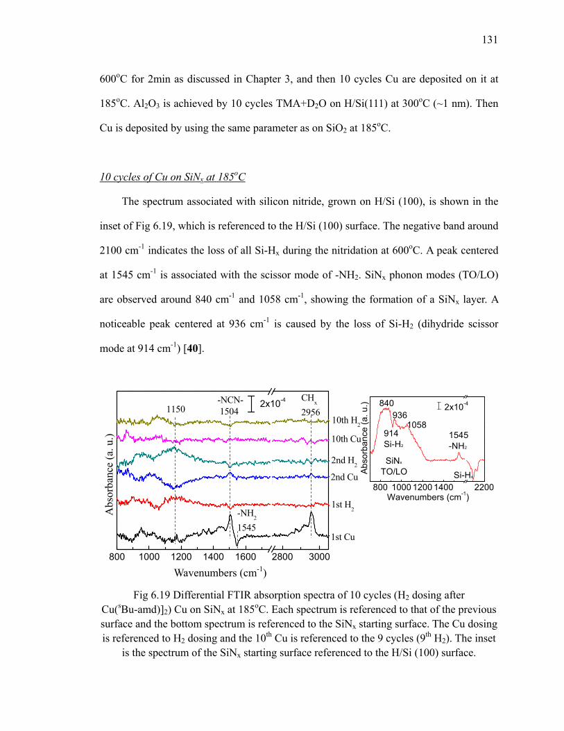
131
600oC for 2min as discussed in Chapter 3, and then 10 cycles Cu are deposited on it at
185oC. Al2O3 is achieved by 10 cycles TMA+D2O on H/Si(111) at 300oC (~1 nm). Then
Cu is deposited by using the same parameter as on SiO2 at 185oC.
10 cycles of Cu on SiNx at 185oC
The spectrum associated with silicon nitride, grown on H/Si (100), is shown in the
inset of Fig 6.19, which is referenced to the H/Si (100) surface. The negative band around
2100 cm-1 indicates the loss of all Si-Hx during the nitridation at 600oC. A peak centered
at 1545 cm-1 is associated with the scissor mode of -NH2. SiNx phonon modes (TO/LO)
are observed around 840 cm-1 and 1058 cm-1, showing the formation of a SiNx layer. A
noticeable peak centered at 936 cm-1 is caused by the loss of Si-H2 (dihydride scissor
mode at 914 cm-1) [40].
800 1000 1200 1400 1600 2800 3000
2nd H2
2nd Cu
1st H2
1st Cu
CHx
2956
-NH2
1545
-NCN- 1504
2x10⁻⁴
115010th H2
10th Cu
Fig 6.19 Differential FTIR absorption spectra of 10 cycles (H2 dosing after
Cu(sBu-amd)]2) Cu on SiNx at 185oC. Each spectrum is referenced to that of the previous surface and the bottom spectrum is referenced to the SiNx starting surface. The Cu dosing is referenced to H2 dosing and the 10th Cu is referenced to the 9 cycles (9th H2). The inset
is the spectrum of the SiNx starting surface referenced to the H/Si (100) surface.
800 1000 1200 1400 2200
1058
840
SiNx
TO/LO
936
914Si-H2
1545-NH2
Si-Hx
2x10⁻⁴
Wavenumbers (cm-1)
Abso
rban
ce (a
. u.)
Wavenumbers (cm-1)
Abs
orba
nce
(a. u
.)
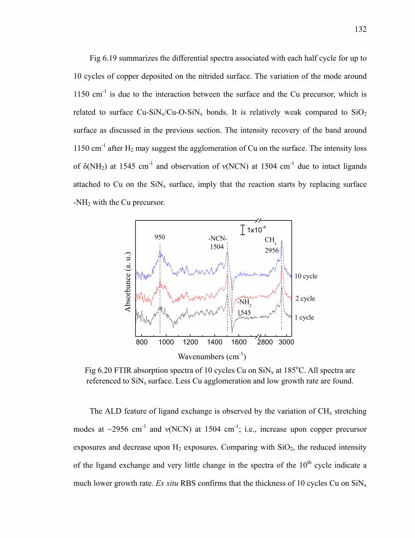
132
Fig 6.19 summarizes the differential spectra associated with each half cycle for up to
10 cycles of copper deposited on the nitrided surface. The variation of the mode around
1150 cm-1 is due to the interaction between the surface and the Cu precursor, which is
related to surface Cu-SiNx/Cu-O-SiNx bonds. It is relatively weak compared to SiO2
surface as discussed in the previous section. The intensity recovery of the band around
1150 cm-1 after H2 may suggest the agglomeration of Cu on the surface. The intensity loss
of δ(NH2) at 1545 cm-1 and observation of ν(NCN) at 1504 cm-1 due to intact ligands
attached to Cu on the SiNx surface, imply that the reaction starts by replacing surface
-NH2 with the Cu precursor.
800 1000 1200 1400 1600 2800 3000
1 cycle
2 cycle
950
-NCN- 1504
CHx
2956
-NH2
1545
1x10⁻⁴
10 cycle
Fig 6.20 FTIR absorption spectra of 10 cycles Cu on SiNx at 185oC. All spectra are referenced to SiNx surface. Less Cu agglomeration and low growth rate are found.
The ALD feature of ligand exchange is observed by the variation of CHx stretching
modes at ~2956 cm-1 and ν(NCN) at 1504 cm-1; i.e., increase upon copper precursor
exposures and decrease upon H2 exposures. Comparing with SiO2, the reduced intensity
of the ligand exchange and very little change in the spectra of the 10th cycle indicate a
much lower growth rate. Ex situ RBS confirms that the thickness of 10 cycles Cu on SiNx
Wavenumbers (cm-1)
Abs
orba
nce
(a. u
.)
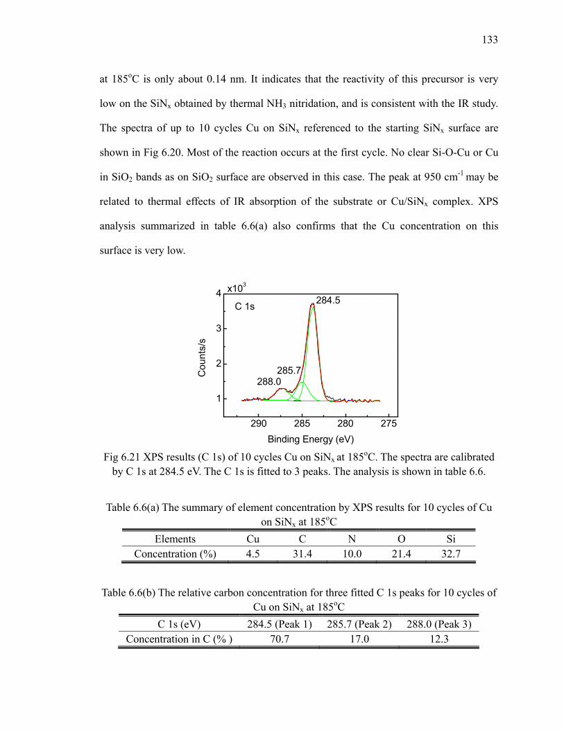
133
at 185oC is only about 0.14 nm. It indicates that the reactivity of this precursor is very
low on the SiNx obtained by thermal NH3 nitridation, and is consistent with the IR study.
The spectra of up to 10 cycles Cu on SiNx referenced to the starting SiNx surface are
shown in Fig 6.20. Most of the reaction occurs at the first cycle. No clear Si-O-Cu or Cu
in SiO2 bands as on SiO2 surface are observed in this case. The peak at 950 cm-1 may be
related to thermal effects of IR absorption of the substrate or Cu/SiNx complex. XPS
analysis summarized in table 6.6(a) also confirms that the Cu concentration on this
surface is very low.
290 285 280 275
1
2
3
4C 1s
285.7288.0
284.5
Cou
nts/
s
Binding Energy (eV)
x103
Fig 6.21 XPS results (C 1s) of 10 cycles Cu on SiNx at 185oC. The spectra are calibrated
by C 1s at 284.5 eV. The C 1s is fitted to 3 peaks. The analysis is shown in table 6.6.
Table 6.6(a) The summary of element concentration by XPS results for 10 cycles of Cu on SiNx at 185oC
Elements Cu C N O Si Concentration (%) 4.5 31.4 10.0 21.4 32.7
Table 6.6(b) The relative carbon concentration for three fitted C 1s peaks for 10 cycles of
Cu on SiNx at 185oC C 1s (eV) 284.5 (Peak 1) 285.7 (Peak 2) 288.0 (Peak 3)
Concentration in C (% ) 70.7 17.0 12.3
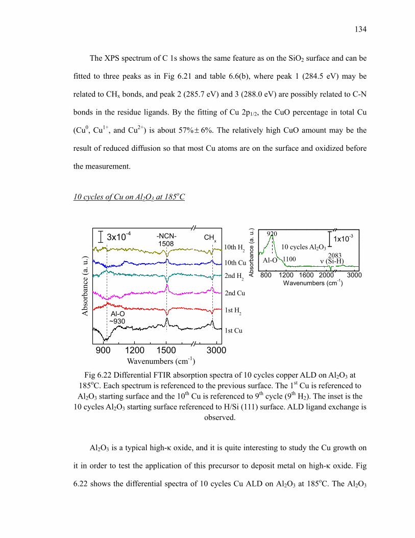
134
The XPS spectrum of C 1s shows the same feature as on the SiO2 surface and can be
fitted to three peaks as in Fig 6.21 and table 6.6(b), where peak 1 (284.5 eV) may be
related to CHx bonds, and peak 2 (285.7 eV) and 3 (288.0 eV) are possibly related to C-N
bonds in the residue ligands. By the fitting of Cu 2p1/2, the CuO percentage in total Cu
(Cu0, Cu1+, and Cu2+) is about 57% ± 6%. The relatively high CuO amount may be the
result of reduced diffusion so that most Cu atoms are on the surface and oxidized before
the measurement.
10 cycles of Cu on Al2O3 at 185oC
900 1200 1500 3000
~9301st H2
3x10⁻⁴
1st Cu
2nd H2
2nd Cu
10th H2
10th Cu
Al-O
1508-NCN- CHx
Fig 6.22 Differential FTIR absorption spectra of 10 cycles copper ALD on Al2O3 at 185oC. Each spectrum is referenced to the previous surface. The 1st Cu is referenced to Al2O3 starting surface and the 10th Cu is referenced to 9th cycle (9th H2). The inset is the
10 cycles Al2O3 starting surface referenced to H/Si (111) surface. ALD ligand exchange is observed.
Al2O3 is a typical high-κ oxide, and it is quite interesting to study the Cu growth on
it in order to test the application of this precursor to deposit metal on high-κ oxide. Fig
6.22 shows the differential spectra of 10 cycles Cu ALD on Al2O3 at 185oC. The Al2O3
Wavenumbers (cm-1)
Abs
orba
nce
(a. u
.)
800 1200 1600 2000 3000
Abs
orba
nce
(a. u
.)
1x10⁻³
Wavenumbers (cm-1)
Al-O ν (Si-H)
10 cycles Al2O3
920
1100 2083
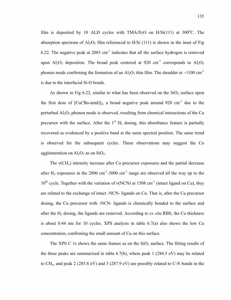
135
film is deposited by 10 ALD cycles with TMA/D2O on H/Si(111) at 300oC. The
absorption spectrum of Al2O3 film referenced to H/Si (111) is shown in the inset of Fig
6.22. The negative peak at 2083 cm-1 indicates that all the surface hydrogen is removed
upon Al2O3 deposition. The broad peak centered at 920 cm-1 corresponds to Al2O3
phonon mode confirming the formation of an Al2O3 thin film. The shoulder at ~1100 cm-1
is due to the interfacial Si-O bonds.
As shown in Fig 6.22, similar to what has been observed on the SiO2 surface upon
the first dose of [Cu(sBu-amd)]2, a broad negative peak around 920 cm-1 due to the
perturbed Al2O3 phonon mode is observed, resulting from chemical interactions of the Cu
precursor with the surface. After the 1st H2 dosing, this absorbance feature is partially
recovered as evidenced by a positive band at the same spectral position. The same trend
is observed for the subsequent cycles. These observations may suggest the Cu
agglomeration on Al2O3 as on SiO2.
The ν(CHx) intensity increase after Cu precursor exposures and the partial decrease
after H2 exposures in the 2800 cm-1-3000 cm-1 range are observed all the way up to the
10th cycle. Together with the variation of ν(NCN) at 1508 cm-1 (intact ligand on Cu), they
are related to the exchange of intact -NCN- ligands on Cu. That is, after the Cu precursor
dosing, the Cu precursor with -NCN- ligands is chemically bonded to the surface and
after the H2 dosing, the ligands are removed. According to ex situ RBS, the Cu thickness
is about 0.44 nm for 10 cycles. XPS analysis in table 6.7(a) also shows the low Cu
concentration, confirming the small amount of Cu on this surface.
The XPS C 1s shows the same feature as on the SiO2 surface. The fitting results of
the three peaks are summarized in table 6.7(b), where peak 1 (284.5 eV) may be related
to CHx, and peak 2 (285.8 eV) and 3 (287.9 eV) are possibly related to C-N bonds in the
136
residue ligands. According to the fitting of Cu 2p1/2, the CuO percentage in total Cu (Cu0,
Cu1+, and Cu2+) is about 22% ± 5%, which is higher than that of Cu on SiO2 at 185oC and
may also imply less Cu diffusion into Al2O3.
290 285 280
2
4
287.9285.8
284.5C 1sC
ount
s/s
Binding Energy (eV)
x103
Fig 6.23 XPS results (C 1s) of 10 cycles Cu on Al2O3 at 185oC. The spectra are calibrated by C 1s at 284.5 eV. The C1s is fitted to 3 peaks. Table 6.7 shows the XPS analysis
summary.
Table 6.7(a) The summary of element concentration by XPS results for 10 cycles of Cu on Al2O3 at 185oC
Elements Cu C N O Si Al Concentration (%) 6.0 38.0 0.8 20.5 8.8 25.9
Table 6.7(b) The relative carbon concentration for three fitted C 1s peaks10 cycles of Cu
on Al2O3 at 185oC C 1s (eV) 284.5 (Peak 1) 285.8 (Peak 2) 287.9 (Peak 3)
Concentration (%) in C 77.8 10.6 11.6
6.5 Other application: deposition of Cu3N
Including deposition of Cu, this Cu precursor can also be used to deposit nitride with
NH3. According to recent studies, Cu3N has been utilized as a material for optical storage
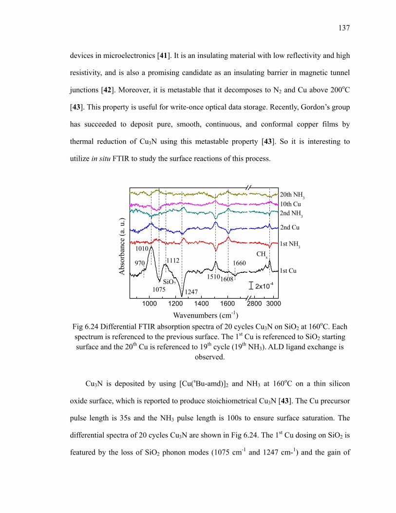
137
devices in microelectronics [41]. It is an insulating material with low reflectivity and high
resistivity, and is also a promising candidate as an insulating barrier in magnetic tunnel
junctions [42]. Moreover, it is metastable that it decomposes to N2 and Cu above 200oC
[43]. This property is useful for write-once optical data storage. Recently, Gordon’s group
has succeeded to deposit pure, smooth, continuous, and conformal copper films by
thermal reduction of Cu3N using this metastable property [43]. So it is interesting to
utilize in situ FTIR to study the surface reactions of this process.
1000 1200 1400 1600 2800 3000
CHx
1608
1660
1510
1112
1075 1247
1010 2x10⁻⁴
970
2nd NH3
2nd Cu
1st NH3
1st Cu
20th NH3
10th Cu
Fig 6.24 Differential FTIR absorption spectra of 20 cycles Cu3N on SiO2 at 160oC. Each spectrum is referenced to the previous surface. The 1st Cu is referenced to SiO2 starting surface and the 20th Cu is referenced to 19th cycle (19th NH3). ALD ligand exchange is
observed.
Cu3N is deposited by using [Cu(sBu-amd)]2 and NH3 at 160oC on a thin silicon
oxide surface, which is reported to produce stoichiometrical Cu3N [43]. The Cu precursor
pulse length is 35s and the NH3 pulse length is 100s to ensure surface saturation. The
differential spectra of 20 cycles Cu3N are shown in Fig 6.24. The 1st Cu dosing on SiO2 is
featured by the loss of SiO2 phonon modes (1075 cm-1 and 1247 cm-1) and the gain of
Wavenumbers (cm-1)
Abs
orba
nce
(a. u
.)
SiO2

138
Si-O-Cu mode (1010 cm-1) as well as the Cu diffusion in SiO2 modes (970 cm-1 and 1112
cm-1). The loss of -OH bending mode at 1660 cm-1 indicates the replacement of -OH
group by the Cu precursor. The 1st NH3 exposure reacts with the intact ligand [ν(NCN) at
1510 cm-1] from the previous Cu precursor dosing. The appearance of the band at 1608
cm-1 indicates that a big part of the intact ligands are not removed but rearranged by NH3.
Therefore, only a part of ν(CHx) around 2956 cm-1 is reduced. A little Cu agglomeration is
observed by the weak band at 1247 cm-1 in the spectrum of the 1st NH3 dosing.
800 1000 1200 1400 1600 2800 3000
20 cycle
10 cycle
1 cycle
4x10⁻⁴
16081510
1660
CHx
1112
12471075
1010
970
Fig 6.25 FTIR absorption spectra of 20 cycles Cu3N on SiO2 at 160oC. All spectra are referenced to SiO2 surface. Less Cu diffusion and some ligand related impurities are
observed in the spectra. The growth rate is low.
There is an increase of the intact ligand upon the 2nd Cu pulse as evidenced by a
positive 1510 cm-1 peak. This 2nd Cu pulse also removes the rearranged ligand band at
1608 cm-1 as shown in the previous section. The variation in the SiO2 phonon modes
suggests that the previous NH3 dosing reacts with the ligand on the surface, recovering
more reaction sites on the SiO2 surface for the subsequent Cu precursor. For the
following cycles, the same scheme continues. The decreased ligand feature for 20th cycle
indicates the growth rate decreases with more ALD cycles.
SiO2
Wavenumbers (cm-1)
Abs
orba
nce
(a. u
.)
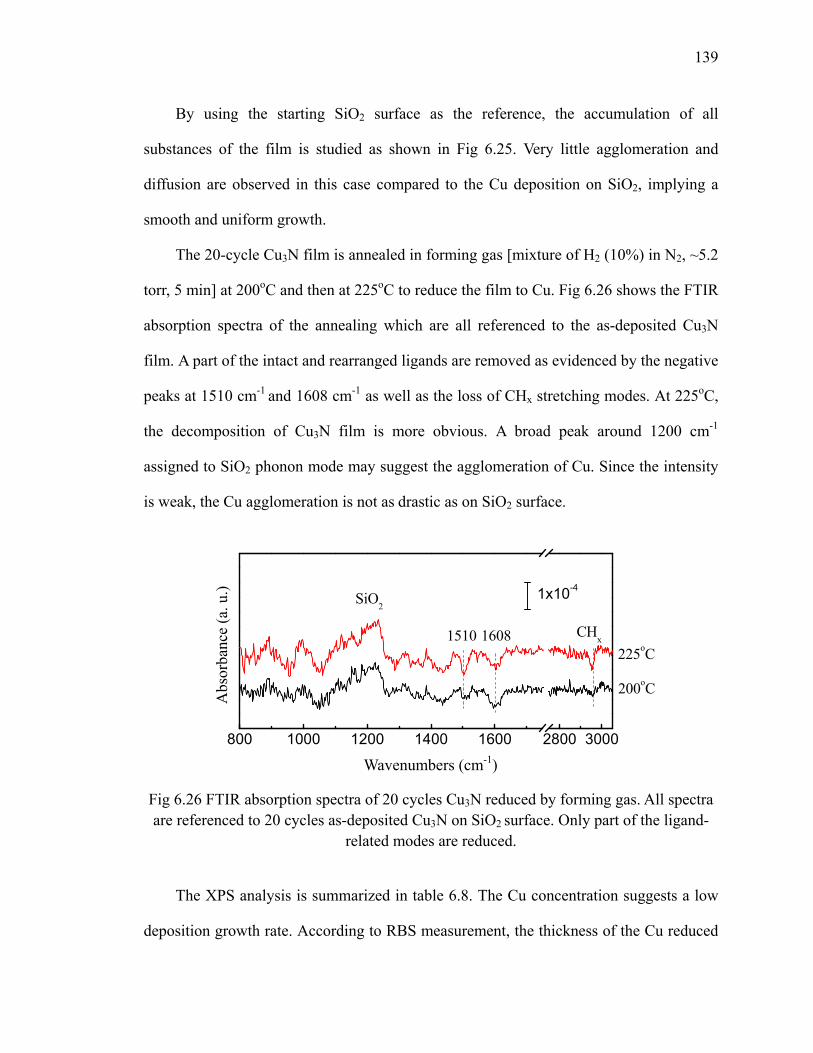
139
By using the starting SiO2 surface as the reference, the accumulation of all
substances of the film is studied as shown in Fig 6.25. Very little agglomeration and
diffusion are observed in this case compared to the Cu deposition on SiO2, implying a
smooth and uniform growth.
The 20-cycle Cu3N film is annealed in forming gas [mixture of H2 (10%) in N2, ~5.2
torr, 5 min] at 200oC and then at 225oC to reduce the film to Cu. Fig 6.26 shows the FTIR
absorption spectra of the annealing which are all referenced to the as-deposited Cu3N
film. A part of the intact and rearranged ligands are removed as evidenced by the negative
peaks at 1510 cm-1 and 1608 cm-1 as well as the loss of CHx stretching modes. At 225oC,
the decomposition of Cu3N film is more obvious. A broad peak around 1200 cm-1
assigned to SiO2 phonon mode may suggest the agglomeration of Cu. Since the intensity
is weak, the Cu agglomeration is not as drastic as on SiO2 surface.
800 1000 1200 1400 1600 2800 3000
CHx1510
200oC
1x10⁻⁴
225oC
SiO2
1608
Fig 6.26 FTIR absorption spectra of 20 cycles Cu3N reduced by forming gas. All spectra are referenced to 20 cycles as-deposited Cu3N on SiO2 surface. Only part of the ligand-
related modes are reduced.
The XPS analysis is summarized in table 6.8. The Cu concentration suggests a low
deposition growth rate. According to RBS measurement, the thickness of the Cu reduced
Wavenumbers (cm-1)
Abs
orba
nce
(a. u
.)
140
from 20-cycle Cu3N is ~0.34 nm.
Table 6.8 The summary of element concentration by XPS results for 20 cycles of reduced
Cu3N Elements Cu C N O Si
Concentration (%) 9.8 40.1 2.1 34.2 13.8
6.6 Summary
As a summary of this chapter, we successfully deposited copper using a novel liquid
Cu precursor--copper(I) di-sec-butylacetamidinate ([Cu(sBu-amd)]2) and molecular
hydrogen on different substrates. The gas phase IR spectrum shows that the precursor is
partially hydrolyzed. In-situ FTIR spectroscopy, ex situ RBS, and XPS are used to study
the ALD processes with the temperature range from 100oC to 300oC. On oxidized Si(100)
surfaces (~6-10 nm SiO2), the evolution of SiO2 phonon modes in the IR spectra clearly
shows the agglomeration and the diffusion of Cu on/into SiO2 during the initial 10 cycles.
Cu agglomeration and diffusion increase when the deposition temperature is raised. The
hydrogen reduction of the surface ligand and ligand rearrangement are observed by the
modes attributed to CHx and -NCN- bonds.
Ex situ XPS results confirm the deposition of copper on the SiO2 surface. Both FTIR
and XPS results show residue ligand impurities inside the Cu film with small amount of
N (< 2%) and substantial amount of C for the initial cycles due to incomplete ALD
reactions. The Cu growth rate is determined by ex situ RBS measurements. The
maximum growth rate on SiO2 is found in the range of 185-250oC based on one ALD
cycle. At 185oC, the thickness of 10 cycles Cu is 1.04-1.18 nm, and the film is very
uniform.
The Cu deposition at 185oC on other surfaces are studied as well, such as the
141
hydrogen -terminated Si(111) and Si (100), nitrided Si(100) (SiNx) and Al2O3 surfaces.
FTIR and XPS show the similar film contents and growth mechanism as on SiO2.
However, much lower growth rate is found for all those surfaces than that of SiO2 surface;
i.e., 0.09 nm on H/Si(111), 0.14 nm on SiNx and 0.44 nm on Al2O3 after 10 ALD cycles.
This indicates that [Cu(sBu-amd)]2 has low adhesion on those surfaces.
At last, Cu3N is deposited on SiO2 at 160oC successfully. The ligand exchange of the
ALD process is observed by FTIR. After annealing at 225oC in forming gas, the Cu3N is
partially reduced to Cu with little Cu agglomeration. FTIR spectra show the incomplete
loss of CHx and ligand bands, and XPS analysis confirms the residue C and N impurities.
Bibliography 1. R. G. Gordon, D. M. Hausmann, E. Kim and J. Shepard, A kinetic model for step coverage by atomic layer deposition in narrow holes or trenches, Chemical Vapor Deposition 9 (2003), 83. 2. B. S. Lim, A. Rahtu and R. G. Gordon, Atomic layer deposition of transition metals, Nature Materials 2 (2003), 749-754. 3. J. Marika, R. Mikko and L. Markku, Deposition of copper films by an alternate supply of CuCl and Zn, Journal of Vacuum Science & Technology A 15 (1997), no. 4, 2330-2333. 4. C. Musgrave and R. G. Gordon, Precursors for atomic layer deposition of high-k dielectrics, Future Fab International 18 (2005), 126-128. 5. The international technology roadmap for semiconductors, semiconductor industry association, http://pulic.itrs.net. (2005). 6. K. Jae Jeong, K. Soo-Kil, L. Chang Hwa and K. Yong Shik, Investigation of various copper seed layers for copper electrodeposition applicable to ultralarge-scale integration interconnection, Journal of Vacuum Science & Technology B 21 (2003), no. 1, 33-38. 7. P. Martensson and J.-O. Carlsson, Atomic layer epitaxy of copper on tantalum, Chemical Vapor Deposition 3 (1997), no. 1, 45-50. 8. M. Per and C. Jan-Otto, Atomic layer epitaxy of copper, Journal of the Electrochemical Society 145 (1998), no. 8, 2926-2931. 9. J. Christopher, W. A. Lanford, J. W. Christopher, J. P. Singh, I. W. Pei, J. S. Jay and L. Toh-Ming, Inductively coupled hydrogen plasma-assisted Cu ALD on metallic and dielectric surfaces, Journal of the Electrochemical Society 152 (2005), no. 2, C60-C64. 10. S. Raj and P. Balu, Atomic layer deposition of copper seed layers, Electrochemical
142
and Solid-State Letters 3 (2000), no. 10, 479-480. 11. J. Huo, R. Solanki and J. McAndrew, Characteristics of copper films produced via atomic layer deposition, Journal of Materials Research 17 (2002), 2394-2398. 12. M. Utriainen, M. Kröger-Laukkanen, L.-S. Johansson and L. Niinist, Studies of metallic thin film growth in an atomic layer epitaxy reactor using M(acac)2 (M=Mi, Cu, Pt) precursors, Applied Surface Science 157 (2000), no. 3, 151-158. 13. N. Antti, R. Antti, S. Timo, A. Kai, R. Mikko and L. Markku, Radical-enhanced atomic layer deposition of metallic copper thin films, Journal of the Electrochemical Society 152 (2005), no. 1, G25-G28. 14. Z. Li, A. Rahtu and R. G. Gordon, Atomic layer deposition of ultrathin copper metal films from a liquid copper(I) amidinate precursor, Journal of Electrochemical Society 153 (2006), C787-C794. 15. N. Benouattas, A. Mosser, D. Raiser, J. Faerber and A. Bouabellou, Behaviour of copper atoms in annealed Cu/SiOx/Si systems, Applied Surface Science 153 (2000), no. 2-3, 79-84. 16. J. D. McBrayer, R. M. Swanson and T. W. Sigmon, Diffusion of metals in silicon dioxide, Journal of the Electrochemical Society 133 (1986), no. 6, 1242-1246. 17. Z. Li, S. T. Barry and R. G. Gordon, Synthesis and characterization of Cu(I) amidinates as precursors for atomic layer deposition (ALD) of copper metal, Inorganic Chemistry 44 (2005), 1728-1735. 18. Y. J. Chabal, G. S. Higashi, K. Raghavachari and V. A. Burrows, In frared spectroscopy of Si(111) and Si(100) surfaces after HF treatment: Hydrogen termination and surface morphology, J. Vac. Sci. Technol. A 7(3) (1989), 2104. 19. L. Stolt and F. M. D'Heurle, The formation of Cu3Si: Marker experiments, Thin Solid Films 189 (1990), no. 2, 269-274. 20. C. Chin-An, Formation of copper silicides from Cu(100)/Si(100) and Cu(111)/Si(111) structures, Journal of Applied Physics 67 (1990), no. 1, 566-569. 21. R. R. Chromik, W. K. Neils and E. J. Cotts, Thermodynamic and kinetic study of solid state reactions in the Cu-Si system, Journal of Applied Physics 86 (1999), no. 8, 4273-4281. 22. R. T. Conley, Infrared spectroscopy, Allyn and Bacon, Inc. (1972). 23. C.-Y. Yang, J. S. Jeng and J. S. Chen, Grain growth, agglomeration and interfacial reaction of copper interconnects, Thin Solid Films 420-421 (2002), 398-402. 24. Y. Ching-Yu and J. S. Chen, Investigation of copper agglomeration at elevated temperatures, Journal of the Electrochemical Society 150 (2003), no. 12, G826-G830. 25. S. Ishizuka, S. Kato, Y. Okamoto and K. Akimoto, Control of hole carrier density of polycrystalline Cu2O thin films by Si doping, Appl. Phys. Lett. 80 (2002), 950. 26. H. Kim and J. Jand, Infrared spectroscopic study of SiOx film formation and decomposition of vinyl silane derivative by heat treatment on copper surface, J. Appl. Polym. Sci. 68 (1998), 785. 27. X. Su, J. Zhao, X. Zhao, Y. Guo, Y. Zhu and ZichenWang, A facile synthesis of
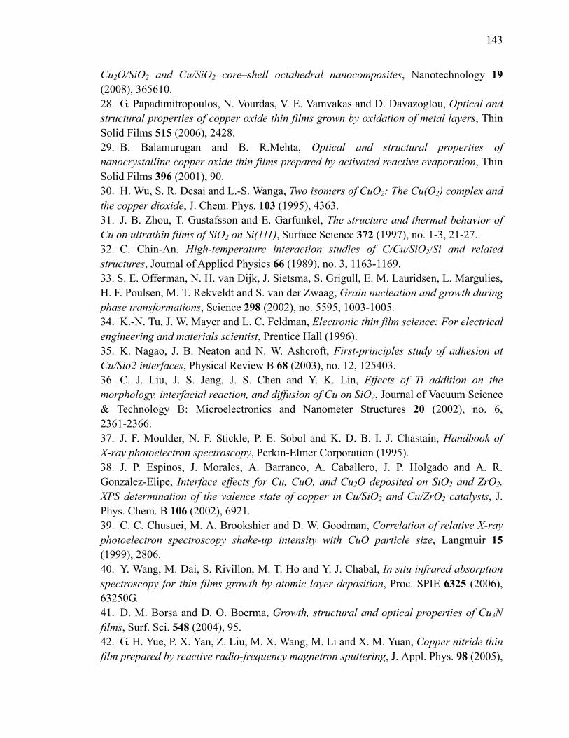
143
Cu2O/SiO2 and Cu/SiO2 core–shell octahedral nanocomposites, Nanotechnology 19 (2008), 365610. 28. G. Papadimitropoulos, N. Vourdas, V. E. Vamvakas and D. Davazoglou, Optical and structural properties of copper oxide thin films grown by oxidation of metal layers, Thin Solid Films 515 (2006), 2428. 29. B. Balamurugan and B. R.Mehta, Optical and structural properties of nanocrystalline copper oxide thin films prepared by activated reactive evaporation, Thin Solid Films 396 (2001), 90. 30. H. Wu, S. R. Desai and L.-S. Wanga, Two isomers of CuO2: The Cu(O2) complex and the copper dioxide, J. Chem. Phys. 103 (1995), 4363. 31. J. B. Zhou, T. Gustafsson and E. Garfunkel, The structure and thermal behavior of Cu on ultrathin films of SiO2 on Si(111), Surface Science 372 (1997), no. 1-3, 21-27. 32. C. Chin-An, High-temperature interaction studies of C/Cu/SiO2/Si and related structures, Journal of Applied Physics 66 (1989), no. 3, 1163-1169. 33. S. E. Offerman, N. H. van Dijk, J. Sietsma, S. Grigull, E. M. Lauridsen, L. Margulies, H. F. Poulsen, M. T. Rekveldt and S. van der Zwaag, Grain nucleation and growth during phase transformations, Science 298 (2002), no. 5595, 1003-1005. 34. K.-N. Tu, J. W. Mayer and L. C. Feldman, Electronic thin film science: For electrical engineering and materials scientist, Prentice Hall (1996). 35. K. Nagao, J. B. Neaton and N. W. Ashcroft, First-principles study of adhesion at Cu/Sio2 interfaces, Physical Review B 68 (2003), no. 12, 125403. 36. C. J. Liu, J. S. Jeng, J. S. Chen and Y. K. Lin, Effects of Ti addition on the morphology, interfacial reaction, and diffusion of Cu on SiO2, Journal of Vacuum Science & Technology B: Microelectronics and Nanometer Structures 20 (2002), no. 6, 2361-2366. 37. J. F. Moulder, N. F. Stickle, P. E. Sobol and K. D. B. I. J. Chastain, Handbook of X-ray photoelectron spectroscopy, Perkin-Elmer Corporation (1995). 38. J. P. Espinos, J. Morales, A. Barranco, A. Caballero, J. P. Holgado and A. R. Gonzalez-Elipe, Interface effects for Cu, CuO, and Cu2O deposited on SiO2 and ZrO2. XPS determination of the valence state of copper in Cu/SiO2 and Cu/ZrO2 catalysts, J. Phys. Chem. B 106 (2002), 6921. 39. C. C. Chusuei, M. A. Brookshier and D. W. Goodman, Correlation of relative X-ray photoelectron spectroscopy shake-up intensity with CuO particle size, Langmuir 15 (1999), 2806. 40. Y. Wang, M. Dai, S. Rivillon, M. T. Ho and Y. J. Chabal, In situ infrared absorption spectroscopy for thin films growth by atomic layer deposition, Proc. SPIE 6325 (2006), 63250G. 41. D. M. Borsa and D. O. Boerma, Growth, structural and optical properties of Cu3N films, Surf. Sci. 548 (2004), 95. 42. G. H. Yue, P. X. Yan, Z. Liu, M. X. Wang, M. Li and X. M. Yuan, Copper nitride thin film prepared by reactive radio-frequency magnetron sputtering, J. Appl. Phys. 98 (2005),
144
103506. 43. Z. Li and R. G. Gordon, Thin, continuous, and conformal copper films by reduction of atomic layer deposited copper nitride, Chem. Vap. Deposition 12 (2006), 435.

145
Chapter 7: SAMs Modification of H/Si, and ALD of
Al2O3, HfO2 and Cu on SAMs
Self assembled monolayers (SAMs) have been attracting tremendous interest of
current researchers since 1980’s for its excellent physical and chemical properties and
wide applications in many areas [1, 2, 3, 4, 5, 6]. It may show different physical and
chemical properties depending on its structure and composition so that it can be used to
modify the surface for both the wet-chemical control of surface reactivity and the surface
functionalization in molecular growth processes.
Generally, SAMs are prepared by surfactant molecules spontaneously attaching a
monomolecular layer onto different surfaces. Without complicate and expensive
experimental instruments, SAMs can be prepared simply by the putting the substrate into
a solution of the desired molecule and then removing the excess. Typically, the molecules
in a SAM are attached to the surfaces via chemical bonds which are dense and
well-ordered exhibiting higher stability than normal organic thin films [7].
SAM is an ideal system that allows fundamental studies of interfacial chemistry and
self-organization. The examples of the functional head groups of SAMs are -SH, -CN,
-COOH, -NH2, -CH3, and so on. Alkyl thiols on gold [8] and Alkyl silanes [9] on SiO2 are
the most well studied two SAM systems. It can be used as sensors, transducers, protective
layers and has many other applications [1, 5, 10].
Due to the high flexibility of functional head groups of SAMs, they have special
meaning in ALD. By varying the functional head groups to reactive or unreactive groups,
selective ALD growth is achieved [11, 12], and Fig 7.1 shows an example [11]. In
addition, SAMs (alkyl chains) have shown extraordinary electrical properties close to the
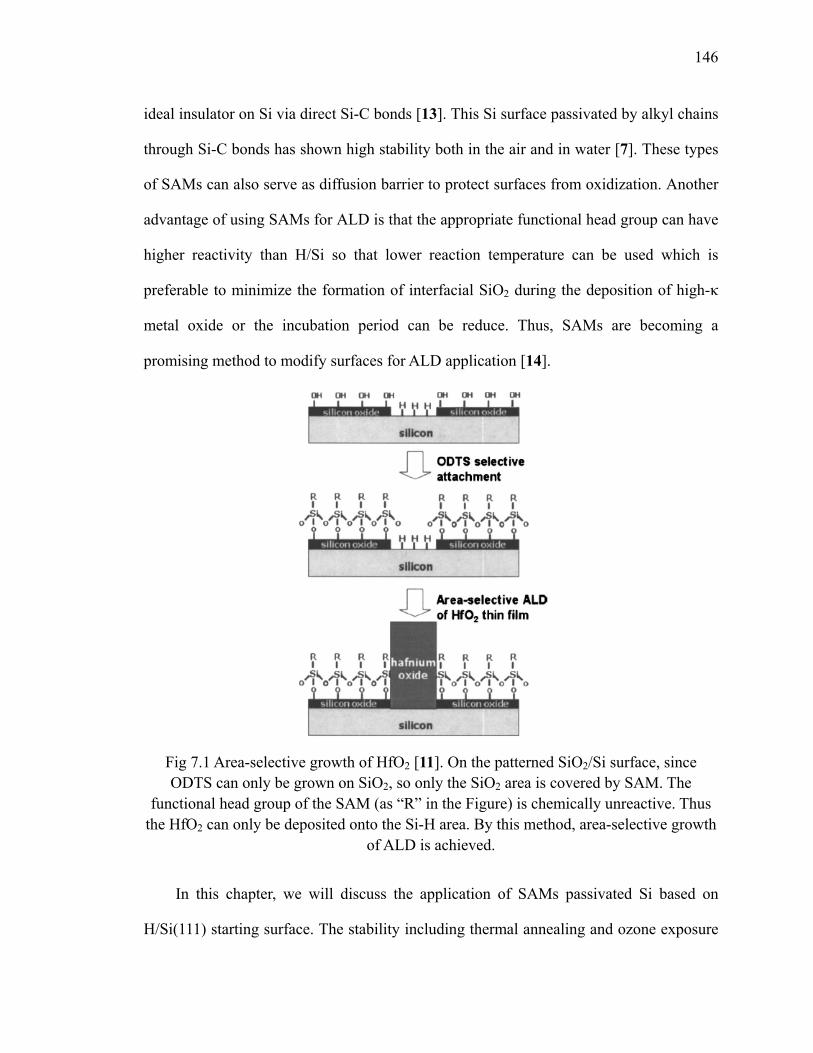
146
ideal insulator on Si via direct Si-C bonds [13]. This Si surface passivated by alkyl chains
through Si-C bonds has shown high stability both in the air and in water [7]. These types
of SAMs can also serve as diffusion barrier to protect surfaces from oxidization. Another
advantage of using SAMs for ALD is that the appropriate functional head group can have
higher reactivity than H/Si so that lower reaction temperature can be used which is
preferable to minimize the formation of interfacial SiO2 during the deposition of high-κ
metal oxide or the incubation period can be reduce. Thus, SAMs are becoming a
promising method to modify surfaces for ALD application [14].
Fig 7.1 Area-selective growth of HfO2 [11]. On the patterned SiO2/Si surface, since ODTS can only be grown on SiO2, so only the SiO2 area is covered by SAM. The
functional head group of the SAM (as “R” in the Figure) is chemically unreactive. Thus the HfO2 can only be deposited onto the Si-H area. By this method, area-selective growth
of ALD is achieved.
In this chapter, we will discuss the application of SAMs passivated Si based on
H/Si(111) starting surface. The stability including thermal annealing and ozone exposure
147
is studied. Then ALD of Al2O3, HfO2 and Cu are deposited on SAMs to investigate the
precursor/surface interaction and film quality for potential applications. Two types of
SAMs are studied, the -CH3 terminated SAM and -COOH terminated SAM, since one
has the chemically unreactive head group and the other has the reactive head group.
7.1 Stability of the -CH3 and -COOH SAMs
-CH3 SAM is prepared as follows: neat 1-octadecene (C18,
) is pre-treated with molecular sieve, and then N2 gas is
bubbled through the solution for at least1 hour to remove the oxygen and H2O. H/Si(111)
sample is placed into the solution for 2 h at 200oC with N2 purging. After the reaction, the
sample is removed and rinsed with THF, dichloromethane and dionized water, and then
dried by N2.
Fig 7.2 The schematic of -CH3 SAM and -COOH SAM. The molecules are directly bond to H/Si(111) surface via Si-C bond. The number of carbon atoms is marked on the left of
the figure.
Similarly, -COOH monolayer is formed via thermal hydrosilylation by
1-undecylenic acid ( ). Fresh H/Si(111) is immersed into
distilled neat deoxygenated 1-undecylenic acid under argon or N2 and heated at 120oC for
2-15h. After the reaction, the derivatized silicon sample is removed, rinsed with ethyl
CH3
H
CH3
H
CH3
18C
Si
OH
H
OH
H
OHO O O
11C
Si-COOH SAM -CH3 SAM
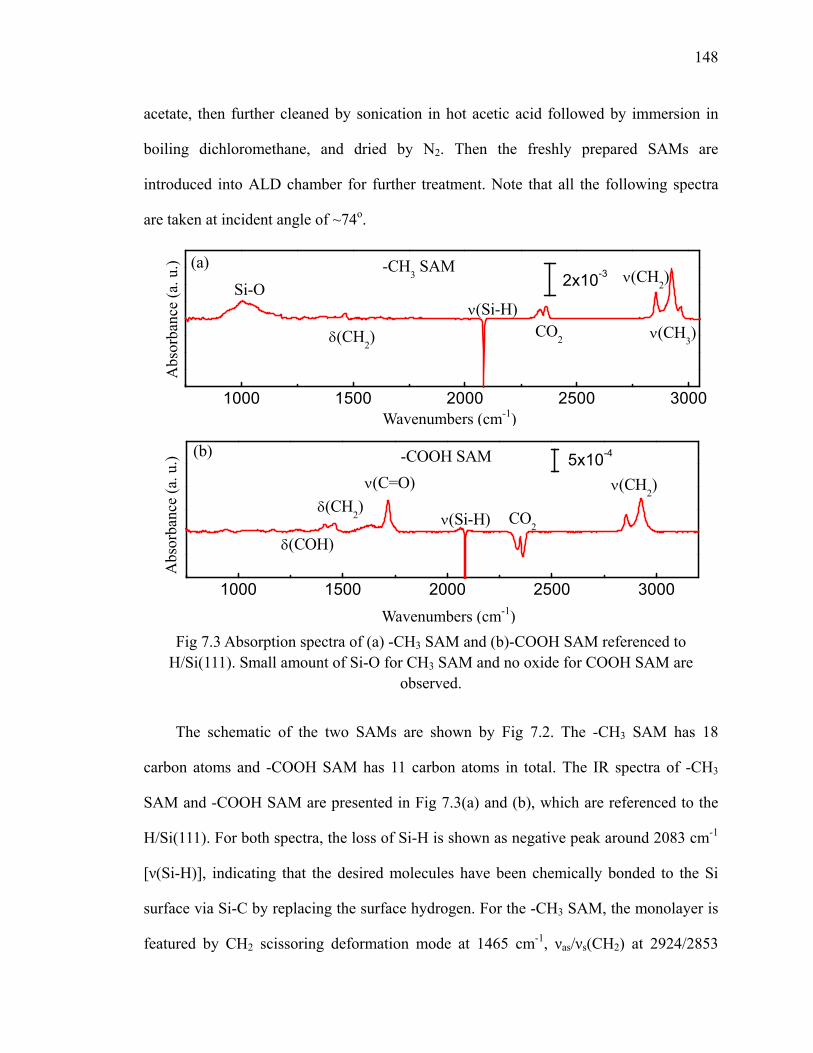
148
acetate, then further cleaned by sonication in hot acetic acid followed by immersion in
boiling dichloromethane, and dried by N2. Then the freshly prepared SAMs are
introduced into ALD chamber for further treatment. Note that all the following spectra
are taken at incident angle of ~74o.
1000 1500 2000 2500 3000
-CH3 SAM(a)
Si-O
δ(CH2)
ν(Si-H)ν(CH3)
2x10⁻³ ν(CH2)
CO2
1000 1500 2000 2500 3000
-COOH SAM
δ(COH)
(b)
ν(C=O)5x10⁻⁴
CO2
δ(CH2) ν(Si-H)
ν(CH2)
Fig 7.3 Absorption spectra of (a) -CH3 SAM and (b)-COOH SAM referenced to
H/Si(111). Small amount of Si-O for CH3 SAM and no oxide for COOH SAM are observed.
The schematic of the two SAMs are shown by Fig 7.2. The -CH3 SAM has 18
carbon atoms and -COOH SAM has 11 carbon atoms in total. The IR spectra of -CH3
SAM and -COOH SAM are presented in Fig 7.3(a) and (b), which are referenced to the
H/Si(111). For both spectra, the loss of Si-H is shown as negative peak around 2083 cm-1
[ν(Si-H)], indicating that the desired molecules have been chemically bonded to the Si
surface via Si-C by replacing the surface hydrogen. For the -CH3 SAM, the monolayer is
featured by CH2 scissoring deformation mode at 1465 cm-1, νas/νs(CH2) at 2924/2853
Wavenumbers (cm-1)
Abs
orba
nce
(a. u
.)
Wavenumbers (cm-1)
Abs
orba
nce
(a. u
.)
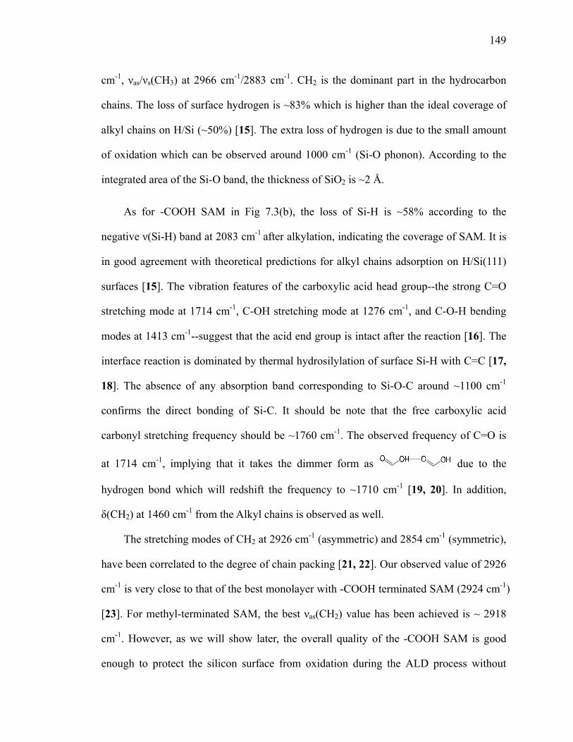
149
cm-1, νas/νs(CH3) at 2966 cm-1/2883 cm-1. CH2 is the dominant part in the hydrocarbon
chains. The loss of surface hydrogen is ~83% which is higher than the ideal coverage of
alkyl chains on H/Si (~50%) [15]. The extra loss of hydrogen is due to the small amount
of oxidation which can be observed around 1000 cm-1 (Si-O phonon). According to the
integrated area of the Si-O band, the thickness of SiO2 is ~2 Å.
As for -COOH SAM in Fig 7.3(b), the loss of Si-H is ~58% according to the
negative ν(Si-H) band at 2083 cm-1 after alkylation, indicating the coverage of SAM. It is
in good agreement with theoretical predictions for alkyl chains adsorption on H/Si(111)
surfaces [15]. The vibration features of the carboxylic acid head group--the strong C=O
stretching mode at 1714 cm-1, C-OH stretching mode at 1276 cm-1, and C-O-H bending
modes at 1413 cm-1--suggest that the acid end group is intact after the reaction [16]. The
interface reaction is dominated by thermal hydrosilylation of surface Si-H with C=C [17,
18]. The absence of any absorption band corresponding to Si-O-C around ~1100 cm-1
confirms the direct bonding of Si-C. It should be note that the free carboxylic acid
carbonyl stretching frequency should be ~1760 cm-1. The observed frequency of C=O is
at 1714 cm-1, implying that it takes the dimmer form as due to the
hydrogen bond which will redshift the frequency to ~1710 cm-1 [19, 20]. In addition,
δ(CH2) at 1460 cm-1 from the Alkyl chains is observed as well.
The stretching modes of CH2 at 2926 cm-1 (asymmetric) and 2854 cm-1 (symmetric),
have been correlated to the degree of chain packing [21, 22]. Our observed value of 2926
cm-1 is very close to that of the best monolayer with -COOH terminated SAM (2924 cm-1)
[23]. For methyl-terminated SAM, the best νas(CH2) value has been achieved is ~ 2918
cm-1. However, as we will show later, the overall quality of the -COOH SAM is good
enough to protect the silicon surface from oxidation during the ALD process without
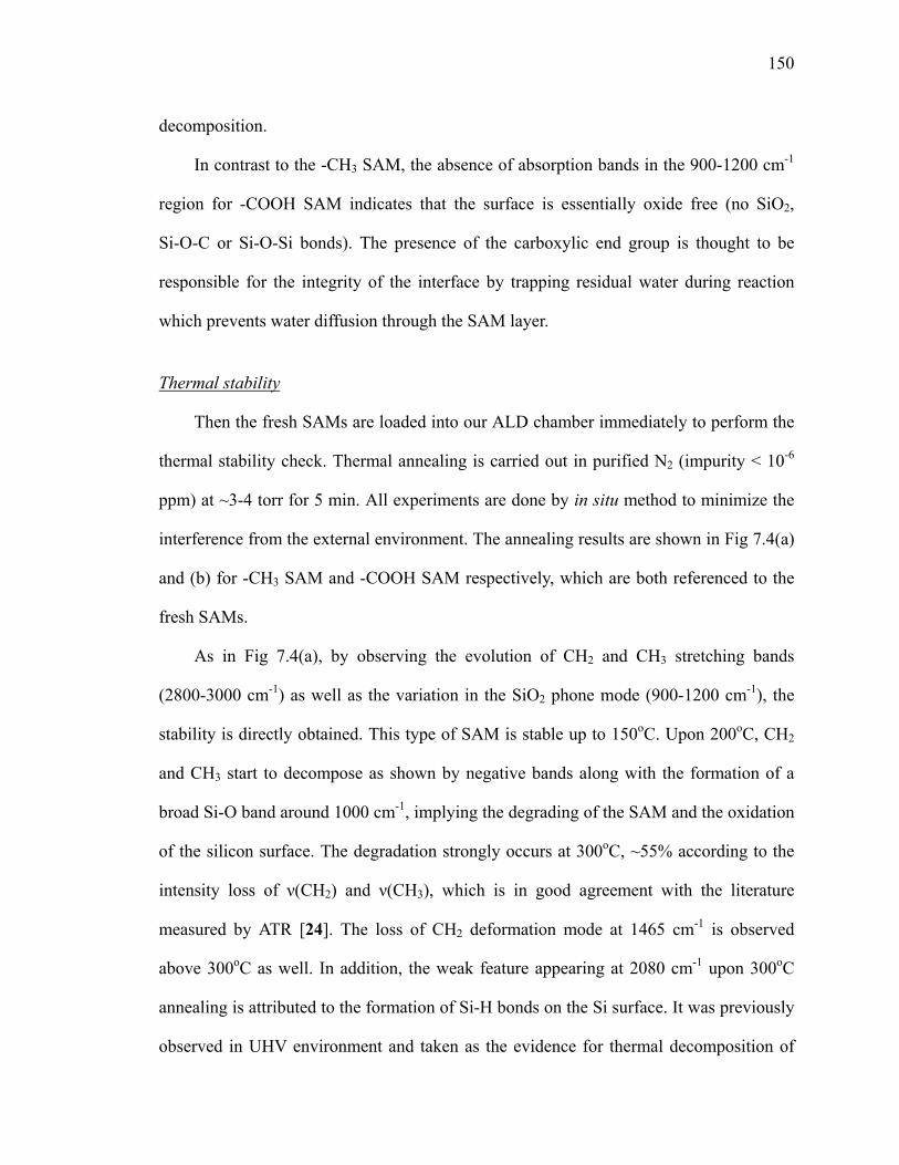
150
decomposition.
In contrast to the -CH3 SAM, the absence of absorption bands in the 900-1200 cm-1
region for -COOH SAM indicates that the surface is essentially oxide free (no SiO2,
Si-O-C or Si-O-Si bonds). The presence of the carboxylic end group is thought to be
responsible for the integrity of the interface by trapping residual water during reaction
which prevents water diffusion through the SAM layer.
Thermal stability
Then the fresh SAMs are loaded into our ALD chamber immediately to perform the
thermal stability check. Thermal annealing is carried out in purified N2 (impurity < 10-6
ppm) at ~3-4 torr for 5 min. All experiments are done by in situ method to minimize the
interference from the external environment. The annealing results are shown in Fig 7.4(a)
and (b) for -CH3 SAM and -COOH SAM respectively, which are both referenced to the
fresh SAMs.
As in Fig 7.4(a), by observing the evolution of CH2 and CH3 stretching bands
(2800-3000 cm-1) as well as the variation in the SiO2 phone mode (900-1200 cm-1), the
stability is directly obtained. This type of SAM is stable up to 150oC. Upon 200oC, CH2
and CH3 start to decompose as shown by negative bands along with the formation of a
broad Si-O band around 1000 cm-1, implying the degrading of the SAM and the oxidation
of the silicon surface. The degradation strongly occurs at 300oC, ~55% according to the
intensity loss of ν(CH2) and ν(CH3), which is in good agreement with the literature
measured by ATR [24]. The loss of CH2 deformation mode at 1465 cm-1 is observed
above 300oC as well. In addition, the weak feature appearing at 2080 cm-1 upon 300oC
annealing is attributed to the formation of Si-H bonds on the Si surface. It was previously
observed in UHV environment and taken as the evidence for thermal decomposition of
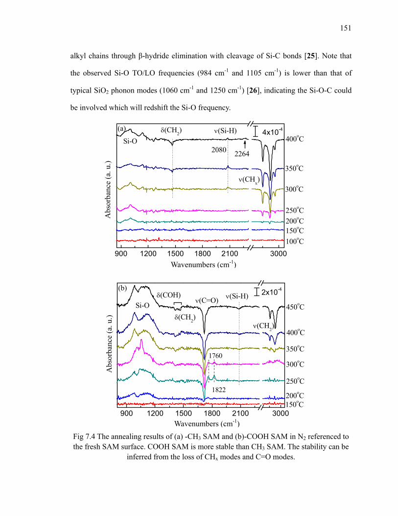
151
alkyl chains through β-hydride elimination with cleavage of Si-C bonds [25]. Note that
the observed Si-O TO/LO frequencies (984 cm-1 and 1105 cm-1) is lower than that of
typical SiO2 phonon modes (1060 cm-1 and 1250 cm-1) [26], indicating the Si-O-C could
be involved which will redshift the Si-O frequency.
900 1200 1500 1800 2100 3000
150oC
250oC200oC
100oC
2080 2264
4x10⁻⁴
ν(CHx)
ν(Si-H)δ(CH2)Si-O
300oC
400oC
350oC
(a)
900 1200 1500 1800 2100 3000
1760
1822
Si-O
2x10⁻⁴
ν(CH2)
ν(C=O)δ(COH) ν(Si-H)
δ(CH2)
400oC
350oC
300oC
250oC
200oC150oC
450oC
(b)
Fig 7.4 The annealing results of (a) -CH3 SAM and (b)-COOH SAM in N2 referenced to the fresh SAM surface. COOH SAM is more stable than CH3 SAM. The stability can be
inferred from the loss of CHx modes and C=O modes.
Wavenumbers (cm-1)
Abs
orba
nce
(a. u
.)
Wavenumbers (cm-1)
Abs
orba
nce
(a. u
.)
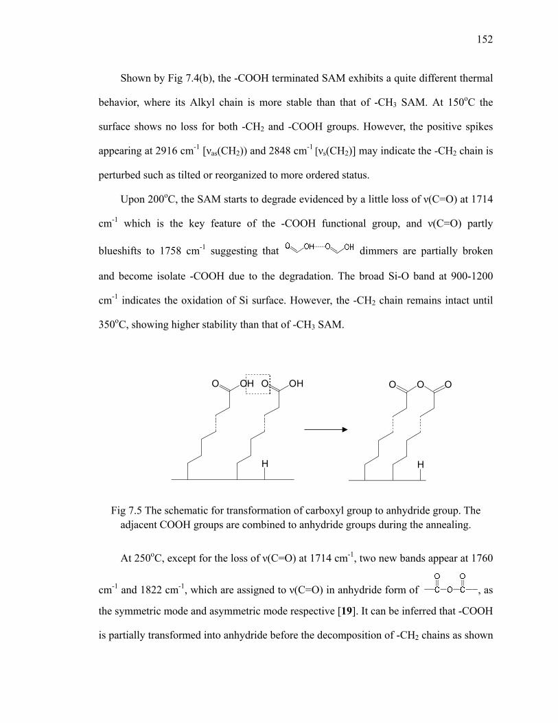
152
Shown by Fig 7.4(b), the -COOH terminated SAM exhibits a quite different thermal
behavior, where its Alkyl chain is more stable than that of -CH3 SAM. At 150oC the
surface shows no loss for both -CH2 and -COOH groups. However, the positive spikes
appearing at 2916 cm-1 [νas(CH2)) and 2848 cm-1 [νs(CH2)] may indicate the -CH2 chain is
perturbed such as tilted or reorganized to more ordered status.
Upon 200oC, the SAM starts to degrade evidenced by a little loss of ν(C=O) at 1714
cm-1 which is the key feature of the -COOH functional group, and ν(C=O) partly
blueshifts to 1758 cm-1 suggesting that dimmers are partially broken
and become isolate -COOH due to the degradation. The broad Si-O band at 900-1200
cm-1 indicates the oxidation of Si surface. However, the -CH2 chain remains intact until
350oC, showing higher stability than that of -CH3 SAM.
Fig 7.5 The schematic for transformation of carboxyl group to anhydride group. The adjacent COOH groups are combined to anhydride groups during the annealing.
At 250oC, except for the loss of ν(C=O) at 1714 cm-1, two new bands appear at 1760
cm-1 and 1822 cm-1, which are assigned to ν(C=O) in anhydride form of , as
the symmetric mode and asymmetric mode respective [19]. It can be inferred that -COOH
is partially transformed into anhydride before the decomposition of -CH2 chains as shown
O O
H
OOH OH
H
O O
153
by the scheme in Fig 7.5, and this process may result in the higher stability for the -CH2
chain of -COOH SAM. Our observations are in good agreement with the literature by
ATR studies [27].
At 350oC, all -COOH decomposes and -CH2 starts to degrade featured by the
intensity loss of CH2 stretching modes at 2800 cm-1-3000 cm-1, C-OH stretching mode at
1276 cm-1 and C-O-H bending modes at 1413 cm-1. The Si-O bands (984 cm-1 and 1105
cm-1) keep increasing with the raising temperature, indicating the cleavage of Si-C bonds
and further oxidation of the surface. At 450oC, the SAM is completely removed from the
surface.
The above studies clearly illustrate the thermal stability of the two types of SAMs.
Only a moderate thermal annealing below 200oC can be performed without substantial
SAM degradation. Based on these, then we can evaluate the ALD application on SAMs.
Stability under ozone exposure
In many cases, ozone is used as oxidant for ALD to minimize the H2O inside the
deposited film to improve its quality. Thus, it is necessary to study the stability of SAMs
when exposed to ozone ambient. For this purpose, -CH3 SAM is exposed to 200 sccm
ozone at 60oC for 2s and -COOH SAM is exposed to 100 sccm ozone for 5s from 60oC to
300 oC. The spectral results are shown in Fig 7.6(a) and (b) which are referenced to the
fresh SAMs.
As shown in Fig 7.6(a), -CH3 SAM is exposed to ozone at 60oC and the spectrum is
referenced to the fresh -CH3 SAM. It can be seen that the Si is oxidized immediately after
the ozone exposure evidenced by the broad Si-O phonon band at 900 cm-1-1200 cm-1. The
intensity loss of ν(CH2) and ν(CH3) (2800 cm-1-3000 cm-1) as the key features of the alkyl
chain confirms the degradation of the SAM by ozone. The data clearly suggests that -CH3
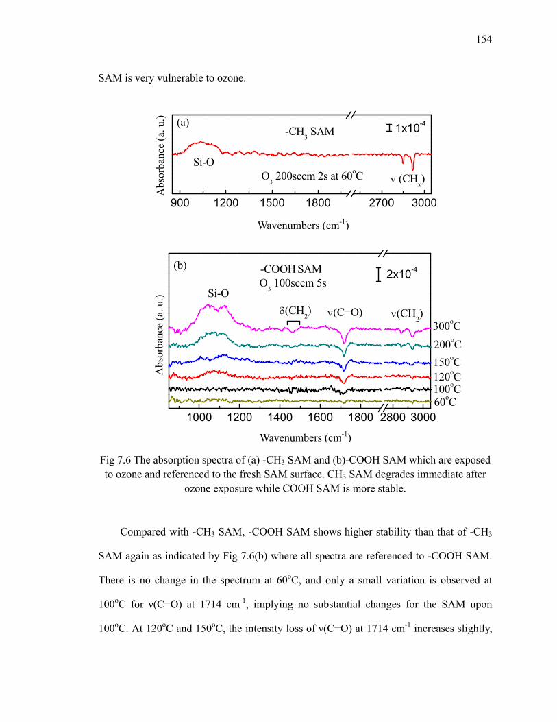
154
SAM is very vulnerable to ozone.
900 1200 1500 1800 2700 3000
(a)
O3 200sccm 2s at 60oC
-CH3 SAM
ν (CHx)Si-O
1x10⁻⁴
1000 1200 1400 1600 1800 2800 3000
(b)O3 100sccm 5s-COOH SAM
60oC100oC120oC
2x10⁻⁴
ν(C=O)δ(CH2)Si-O
ν(CH2)300oC200oC150oC
Fig 7.6 The absorption spectra of (a) -CH3 SAM and (b)-COOH SAM which are exposed to ozone and referenced to the fresh SAM surface. CH3 SAM degrades immediate after
ozone exposure while COOH SAM is more stable.
Compared with -CH3 SAM, -COOH SAM shows higher stability than that of -CH3
SAM again as indicated by Fig 7.6(b) where all spectra are referenced to -COOH SAM.
There is no change in the spectrum at 60oC, and only a small variation is observed at
100oC for ν(C=O) at 1714 cm-1, implying no substantial changes for the SAM upon
100oC. At 120oC and 150oC, the intensity loss of ν(C=O) at 1714 cm-1 increases slightly,
Wavenumbers (cm-1)
Abs
orba
nce
(a. u
.)
Wavenumbers (cm-1)
Abs
orba
nce
(a. u
.)
155
and ν(C=O) partially blueshifts to 1760 cm-1 due to the isolated -COOH groups after the
slight degradation of head groups. The tiny broad band at 900 cm-1-1200 cm-1 may result
from base line fluctuation because of no substantial change for ν(CH2) (2800 cm-1-3000
cm-1), meaning the underlying -CH2 chain remains intact.
Starting from 150oC, the Si surface is being oxidized according the increased Si-O
band with the loss of -CH2 according to the negative ν(CH2) bands. These features
suggest a slight degradation of CH2 chains starting from this temperature. As the
temperature increases, the intensity of Si-O band keeps increasing and the loss of more
ν(CH2) (2800-3000 cm-1) confirms further oxidation of Si surface. Note that the loss of
CH2 deformation mode at 1465 cm-1 is observed at 300oC as well. Compared with
thermal annealing in N2, there is about 50oC temperature difference for the stability since
ozone is much more chemically reactive which makes the SAM more vulnerable.
-COOH SAM is a stable surface. Our study shows that the surface remains
unchanged with N2 purge for days. Even after dipping the -COOH SAM terminated Si
into HF or HCl for minutes, the SAM survives. This monolayer shows high quality
among organic films.
Thus, we checked the stability of two types of SAMs: one with chemically
unreactive methyl functional group, and the other with chemically reactive carboxylic
functional group. The -COOH SAM shows great stability as an ultra thin organic film. It
survives after annealing in N2 or after exposed to ozone at a moderate temperature. It can
be used as one of the surface passivation methods to modify Si surface for ALD
application due to its active functional group and good stability. Next, we will
demonstrate ALD on this surface for both metal and metal oxide, including Al2O3, HfO2
and Cu.
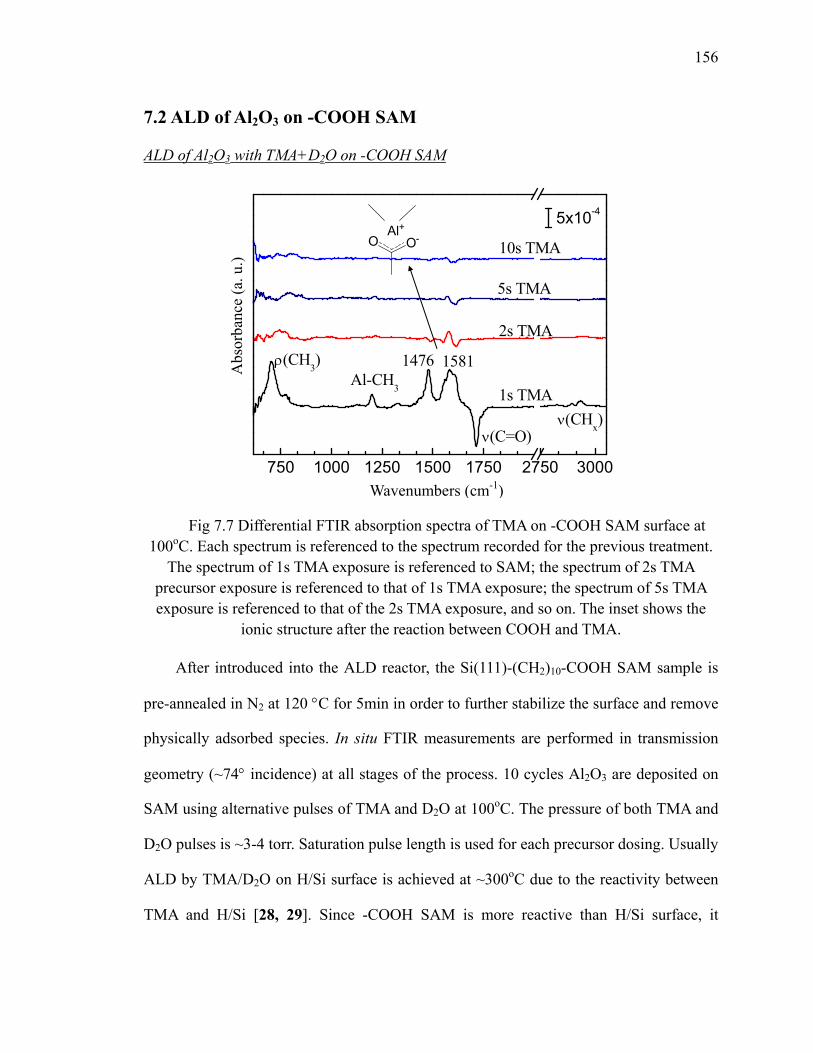
156
7.2 ALD of Al2O3 on -COOH SAM
ALD of Al2O3 with TMA+D2O on -COOH SAM
750 1000 1250 1500 1750 2750 3000
15811476Al-CH3
ρ(CH3)
10s TMA
5s TMA
2s TMA
5x10⁻⁴
1s TMA
ν(C=O)ν(CHx)
Fig 7.7 Differential FTIR absorption spectra of TMA on -COOH SAM surface at 100oC. Each spectrum is referenced to the spectrum recorded for the previous treatment.
The spectrum of 1s TMA exposure is referenced to SAM; the spectrum of 2s TMA precursor exposure is referenced to that of 1s TMA exposure; the spectrum of 5s TMA exposure is referenced to that of the 2s TMA exposure, and so on. The inset shows the
ionic structure after the reaction between COOH and TMA.
After introduced into the ALD reactor, the Si(111)-(CH2)10-COOH SAM sample is
pre-annealed in N2 at 120 °C for 5min in order to further stabilize the surface and remove
physically adsorbed species. In situ FTIR measurements are performed in transmission
geometry (~74° incidence) at all stages of the process. 10 cycles Al2O3 are deposited on
SAM using alternative pulses of TMA and D2O at 100oC. The pressure of both TMA and
D2O pulses is ~3-4 torr. Saturation pulse length is used for each precursor dosing. Usually
ALD by TMA/D2O on H/Si surface is achieved at ~300oC due to the reactivity between
TMA and H/Si [28, 29]. Since -COOH SAM is more reactive than H/Si surface, it
Wavenumbers (cm-1)
Abs
orba
nce
(a. u
.) O O-
Al+
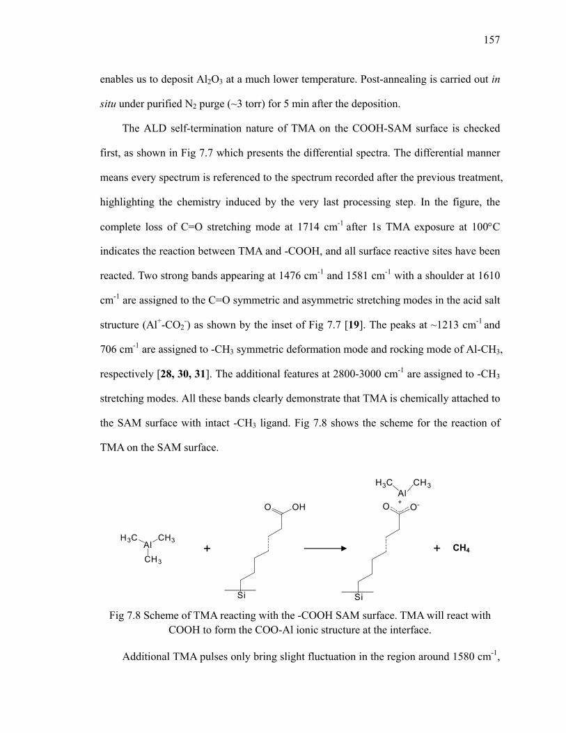
157
enables us to deposit Al2O3 at a much lower temperature. Post-annealing is carried out in
situ under purified N2 purge (~3 torr) for 5 min after the deposition.
The ALD self-termination nature of TMA on the COOH-SAM surface is checked
first, as shown in Fig 7.7 which presents the differential spectra. The differential manner
means every spectrum is referenced to the spectrum recorded after the previous treatment,
highlighting the chemistry induced by the very last processing step. In the figure, the
complete loss of C=O stretching mode at 1714 cm-1 after 1s TMA exposure at 100°C
indicates the reaction between TMA and -COOH, and all surface reactive sites have been
reacted. Two strong bands appearing at 1476 cm-1 and 1581 cm-1 with a shoulder at 1610
cm-1 are assigned to the C=O symmetric and asymmetric stretching modes in the acid salt
structure (Al+-CO2-) as shown by the inset of Fig 7.7 [19]. The peaks at ~1213 cm-1 and
706 cm-1 are assigned to -CH3 symmetric deformation mode and rocking mode of Al-CH3,
respectively [28, 30, 31]. The additional features at 2800-3000 cm-1 are assigned to -CH3
stretching modes. All these bands clearly demonstrate that TMA is chemically attached to
the SAM surface with intact -CH3 ligand. Fig 7.8 shows the scheme for the reaction of
TMA on the SAM surface.
Fig 7.8 Scheme of TMA reacting with the -COOH SAM surface. TMA will react with
COOH to form the COO-Al ionic structure at the interface.
Additional TMA pulses only bring slight fluctuation in the region around 1580 cm-1,
Si
O-OAl+
H3C CH3
Si
OHO
AlCH3H3C
CH3
+ CH4 +
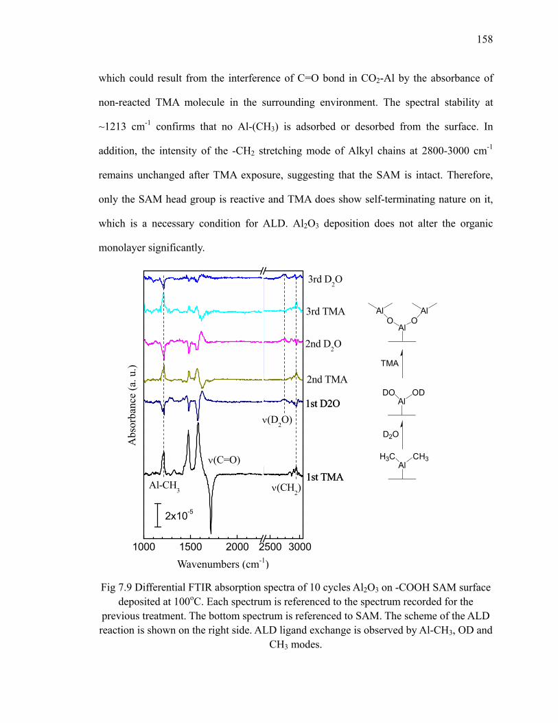
158
which could result from the interference of C=O bond in CO2-Al by the absorbance of
non-reacted TMA molecule in the surrounding environment. The spectral stability at
~1213 cm-1 confirms that no Al-(CH3) is adsorbed or desorbed from the surface. In
addition, the intensity of the -CH2 stretching mode of Alkyl chains at 2800-3000 cm-1
remains unchanged after TMA exposure, suggesting that the SAM is intact. Therefore,
only the SAM head group is reactive and TMA does show self-terminating nature on it,
which is a necessary condition for ALD. Al2O3 deposition does not alter the organic
monolayer significantly.
Fig 7.9 Differential FTIR absorption spectra of 10 cycles Al2O3 on -COOH SAM surface
deposited at 100oC. Each spectrum is referenced to the spectrum recorded for the previous treatment. The bottom spectrum is referenced to SAM. The scheme of the ALD reaction is shown on the right side. ALD ligand exchange is observed by Al-CH3, OD and
CH3 modes.
1000 1500 2000 2500 3000
1st D2O
1st TMAAl-CH3
ν(D2O)
ν(CH2)
2x10⁻⁵
ν(C=O)
1st D2O
1st TMA
2nd D2O
2nd TMA
3rd D2O
3rd TMA
AlH3C CH3
D2O
AlDO OD
Al
TMA
O OAl Al
Wavenumbers (cm-1)
Abs
orba
nce
(a. u
.)
159
The well defined growth of 10 cycles TMA and D2O at 100 °C is shown in Fig 7.9,
where each complete cycle corresponds to one exposure of TMA followed by one
exposure of D2O. The bottom spectrum is referenced to SAM surface and shows the same
features as the 1st TMA exposure in Fig 7.7, where the TMA completely consumes the
accessible COOH groups on the surface to form a complete layer. After the first D2O
exposure, the peak intensity of the deformation and rocking modes of Al-CH3 at 1213 and
~706 cm-1 strongly decreases, as expected due to the hydrolysis of Al-CH3 by D2O
(Al-CH3 is replaced by Al-OD) [32]. The intensity variation associated with modes at
1476 and 1581 cm-1 (i.e. shift to ~1460 cm-1 and ~1624 cm-1) is tentatively attributed to
the environment change of C=O after hydrolysis of Al-CH3. The weak band centered at
2743 cm-1 (OD stretch) confirms that hydrolysis has taken place.
In contrast to the growth of Al2O3 on H/Si (exhibiting interfacial oxidation), there is
no interfacial SiO2 upon water exposure or later on cycles in the ALD process. On the
other hand, CH3 attached to Si (Si-CH3) is the dominant reaction of initial TMA on H/Si
which causes incubation period for ALD growth, while on SAM the Al-CH3 is the
dominant part evidenced by strong and comparable intensity of Al-CH3 methyl
deformation mode (~1213 cm-1) from the 1st TMA to 3rd TMA without any observation of
Si-CH3. This feature indicates less incubation period on SAM and further proves that
-COOH SAM is more favorable for TMA than H/Si.
For the following cycles, the periodic ALD ligand exchange behavior is observed,
showing the layer by layer growth. After the second TMA exposure, TMA reacts with
surface Al-OD groups to form Al-O-Al-CH3, indicated by the Al-CH3 characteristic peak
at 1213 cm-1 and broad Al2O3 band at 700-800cm-1. The subsequent D2O exposure
leading to replacing -CH3 by -OD is as expected. The reversible intensity variation
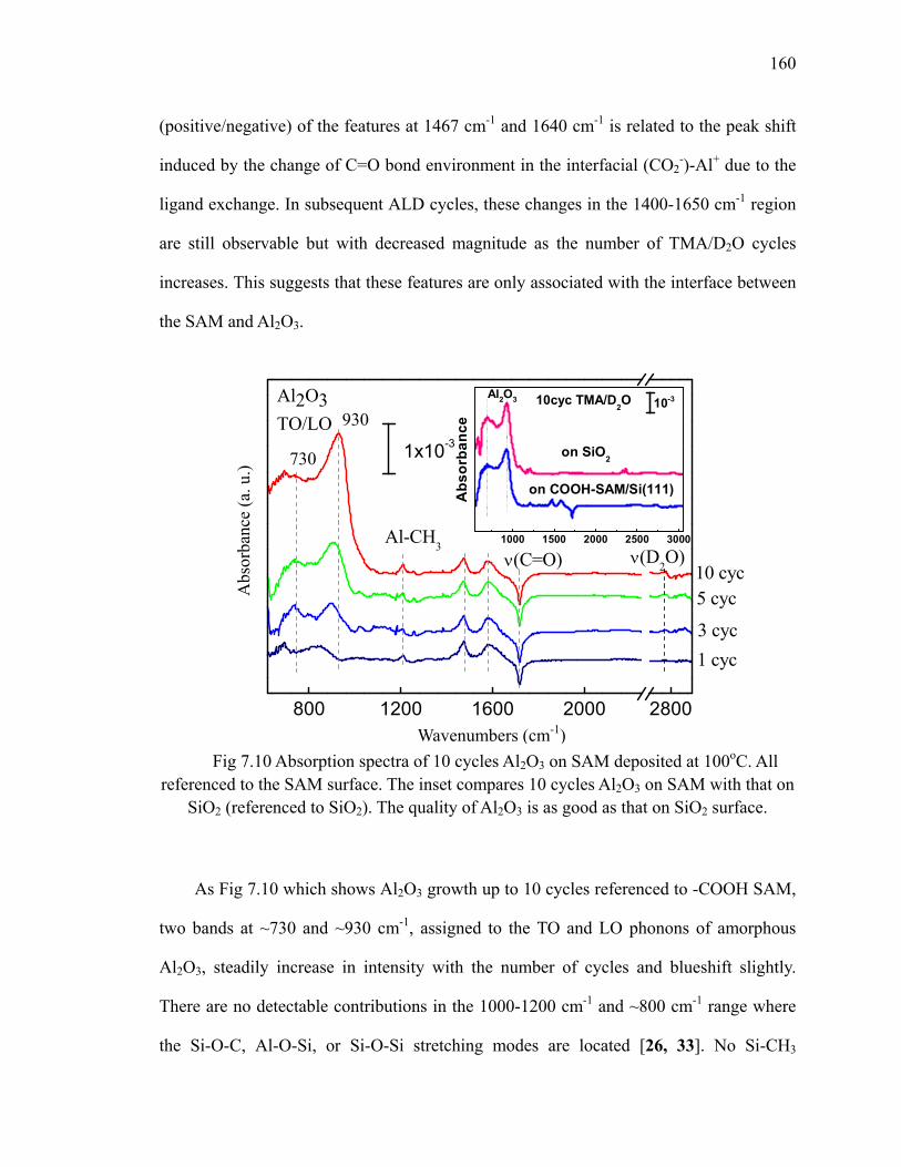
160
(positive/negative) of the features at 1467 cm-1 and 1640 cm-1 is related to the peak shift
induced by the change of C=O bond environment in the interfacial (CO2-)-Al+ due to the
ligand exchange. In subsequent ALD cycles, these changes in the 1400-1650 cm-1 region
are still observable but with decreased magnitude as the number of TMA/D2O cycles
increases. This suggests that these features are only associated with the interface between
the SAM and Al2O3.
Fig 7.10 Absorption spectra of 10 cycles Al2O3 on SAM deposited at 100oC. All referenced to the SAM surface. The inset compares 10 cycles Al2O3 on SAM with that on
SiO2 (referenced to SiO2). The quality of Al2O3 is as good as that on SiO2 surface.
As Fig 7.10 which shows Al2O3 growth up to 10 cycles referenced to -COOH SAM,
two bands at ~730 and ~930 cm-1, assigned to the TO and LO phonons of amorphous
Al2O3, steadily increase in intensity with the number of cycles and blueshift slightly.
There are no detectable contributions in the 1000-1200 cm-1 and ~800 cm-1 range where
the Si-O-C, Al-O-Si, or Si-O-Si stretching modes are located [26, 33]. No Si-CH3
800 1200 1600 2000 2800
ν(D2O)
730
Al-CH3
1 cyc
1000 1500 2000 2500 3000
on SiO2
Al2O3
on COOH-SAM/Si(111)
10cyc TMA/D2O
Abs
orba
nce
10-3
10 cyc5 cyc
3 cyc
930Al2O3TO/LO
ν(C=O)
1x10⁻³
Wavenumbers (cm-1)
Abs
orba
nce
(a. u
.)
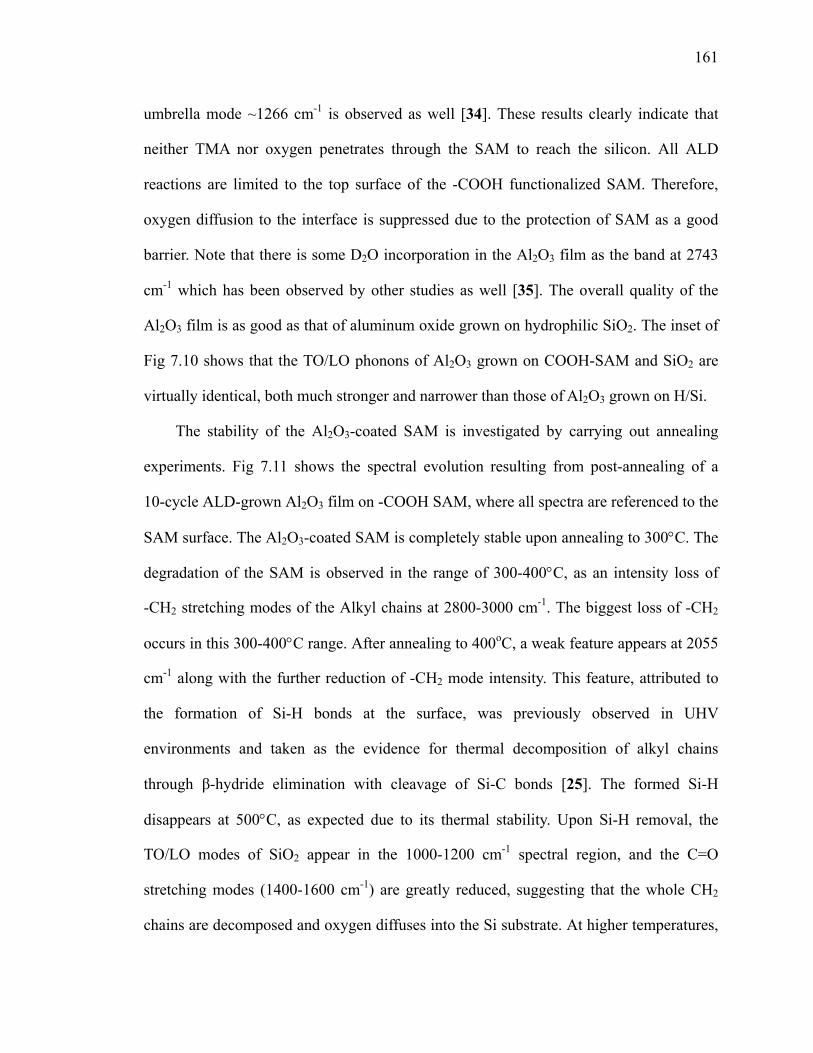
161
umbrella mode ~1266 cm-1 is observed as well [34]. These results clearly indicate that
neither TMA nor oxygen penetrates through the SAM to reach the silicon. All ALD
reactions are limited to the top surface of the -COOH functionalized SAM. Therefore,
oxygen diffusion to the interface is suppressed due to the protection of SAM as a good
barrier. Note that there is some D2O incorporation in the Al2O3 film as the band at 2743
cm-1 which has been observed by other studies as well [35]. The overall quality of the
Al2O3 film is as good as that of aluminum oxide grown on hydrophilic SiO2. The inset of
Fig 7.10 shows that the TO/LO phonons of Al2O3 grown on COOH-SAM and SiO2 are
virtually identical, both much stronger and narrower than those of Al2O3 grown on H/Si.
The stability of the Al2O3-coated SAM is investigated by carrying out annealing
experiments. Fig 7.11 shows the spectral evolution resulting from post-annealing of a
10-cycle ALD-grown Al2O3 film on -COOH SAM, where all spectra are referenced to the
SAM surface. The Al2O3-coated SAM is completely stable upon annealing to 300°C. The
degradation of the SAM is observed in the range of 300-400°C, as an intensity loss of
-CH2 stretching modes of the Alkyl chains at 2800-3000 cm-1. The biggest loss of -CH2
occurs in this 300-400°C range. After annealing to 400oC, a weak feature appears at 2055
cm-1 along with the further reduction of -CH2 mode intensity. This feature, attributed to
the formation of Si-H bonds at the surface, was previously observed in UHV
environments and taken as the evidence for thermal decomposition of alkyl chains
through β-hydride elimination with cleavage of Si-C bonds [25]. The formed Si-H
disappears at 500°C, as expected due to its thermal stability. Upon Si-H removal, the
TO/LO modes of SiO2 appear in the 1000-1200 cm-1 spectral region, and the C=O
stretching modes (1400-1600 cm-1) are greatly reduced, suggesting that the whole CH2
chains are decomposed and oxygen diffuses into the Si substrate. At higher temperatures,
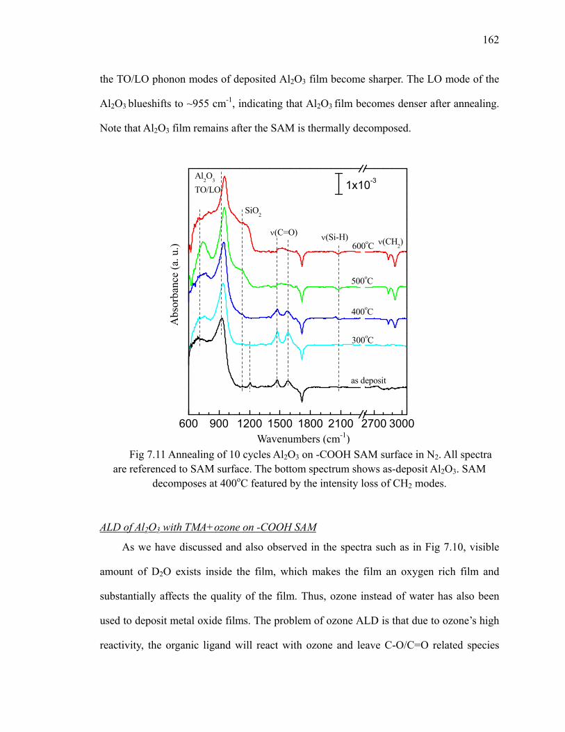
162
the TO/LO phonon modes of deposited Al2O3 film become sharper. The LO mode of the
Al2O3 blueshifts to ~955 cm-1, indicating that Al2O3 film becomes denser after annealing.
Note that Al2O3 film remains after the SAM is thermally decomposed.
600 900 1200 1500 1800 2100 2700 3000
600oC
500oC
400oC
300oC
as deposit
ν(Si-H)ν(C=O)ν(CH2)
SiO2
1x10⁻³
Al2O3
TO/LO
Fig 7.11 Annealing of 10 cycles Al2O3 on -COOH SAM surface in N2. All spectra
are referenced to SAM surface. The bottom spectrum shows as-deposit Al2O3. SAM decomposes at 400oC featured by the intensity loss of CH2 modes.
ALD of Al2O3 with TMA+ozone on -COOH SAM
As we have discussed and also observed in the spectra such as in Fig 7.10, visible
amount of D2O exists inside the film, which makes the film an oxygen rich film and
substantially affects the quality of the film. Thus, ozone instead of water has also been
used to deposit metal oxide films. The problem of ozone ALD is that due to ozone’s high
reactivity, the organic ligand will react with ozone and leave C-O/C=O related species
Wavenumbers (cm-1)
Abs
orba
nce
(a. u
.)
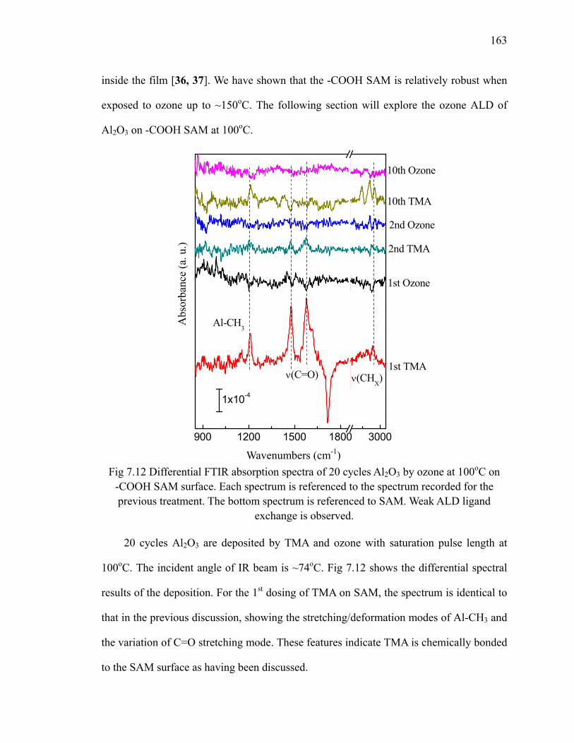
163
inside the film [36, 37]. We have shown that the -COOH SAM is relatively robust when
exposed to ozone up to ~150oC. The following section will explore the ozone ALD of
Al2O3 on -COOH SAM at 100oC.
900 1200 1500 1800 3000
1st Ozone
1x10⁻⁴
1st TMA
2nd Ozone
2nd TMA
10th Ozone
10th TMA
ν(C=O)
Al-CH3
ν(CHX)
Fig 7.12 Differential FTIR absorption spectra of 20 cycles Al2O3 by ozone at 100oC on -COOH SAM surface. Each spectrum is referenced to the spectrum recorded for the previous treatment. The bottom spectrum is referenced to SAM. Weak ALD ligand
exchange is observed.
20 cycles Al2O3 are deposited by TMA and ozone with saturation pulse length at
100oC. The incident angle of IR beam is ~74oC. Fig 7.12 shows the differential spectral
results of the deposition. For the 1st dosing of TMA on SAM, the spectrum is identical to
that in the previous discussion, showing the stretching/deformation modes of Al-CH3 and
the variation of C=O stretching mode. These features indicate TMA is chemically bonded
to the SAM surface as having been discussed.
Wavenumbers (cm-1)
Abs
orba
nce
(a. u
.)

164
Upon the subsequent ozone exposure, the tiny negative band of ν(CHx) at 2800-3000
cm-1 shows the reaction of Al-CH3 methyl ligands with ozone. The weak and reversible
intensity variation of the features at 1476 and 1581 cm-1 is related to the peak shift
induced by the change of C=O bond environment in the interfacial (CO2)-Al from
Al-CH3 to Al-O-Al. The detailed reactions between TMA and ozone have been discussed
in the previous chapter for ozone ALD. Shown by the spectra, methyl ligand is not
completely removed especially for the 1st cycle, meaning an insufficient ALD ligand
exchange which will lower the deposition rate. The following cycles repeat the same
scheme: after TMA dosing, Al-CH3 is adsorbed onto the surface; after ozone dosing, the
methyl ligand is partially removed.
900 1200 1500 1800 3000
ν(C=O) ν(C-O)Al2O3
4x10⁻⁴
ν(CHX)Al-CH3
20 cyc10 cyc
2 cyc
1 cyc
Fig 7.13 Absorption spectra of 20 cycles Al2O3 by ozone on SAM. All referenced to the SAM surface. Al2O3 and substantial carbonated species are observed. The CH2 intensity
loss indicates the degradation of SAM.
Although tiny changes are observed in the differential spectra, when we reference
the spectra to SAM surface as in Fig 7.13, the Al-O phonon mode centered at ~905 cm-1
is observed and indicates the formation of Al2O3. The Al-CH3 methyl deformation mode
Wavenumbers (cm-1)
Abs
orba
nce
(a. u
.)
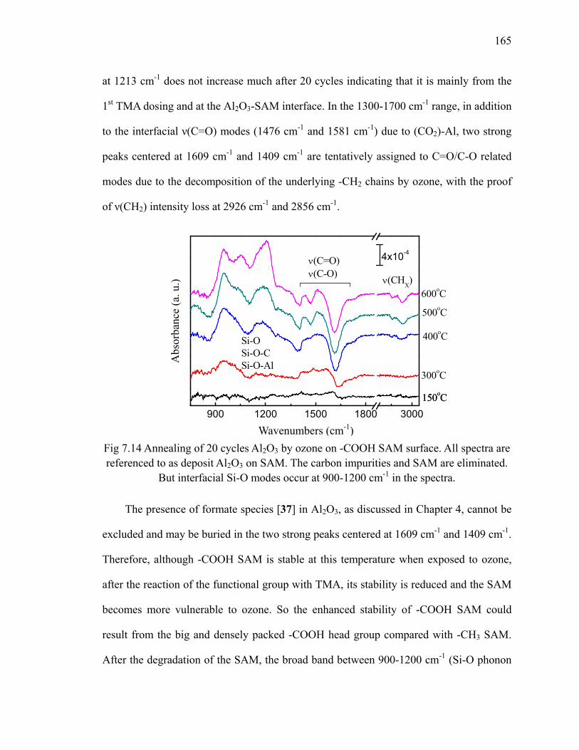
165
at 1213 cm-1 does not increase much after 20 cycles indicating that it is mainly from the
1st TMA dosing and at the Al2O3-SAM interface. In the 1300-1700 cm-1 range, in addition
to the interfacial ν(C=O) modes (1476 cm-1 and 1581 cm-1) due to (CO2)-Al, two strong
peaks centered at 1609 cm-1 and 1409 cm-1 are tentatively assigned to C=O/C-O related
modes due to the decomposition of the underlying -CH2 chains by ozone, with the proof
of ν(CH2) intensity loss at 2926 cm-1 and 2856 cm-1.
900 1200 1500 1800 3000
600oC
500oC
400oC
300oC
150oC150oC
4x10⁻⁴
Si-OSi-O-CSi-O-Al
ν(C=O)ν(C-O)
ν(CHX)
Fig 7.14 Annealing of 20 cycles Al2O3 by ozone on -COOH SAM surface. All spectra are referenced to as deposit Al2O3 on SAM. The carbon impurities and SAM are eliminated.
But interfacial Si-O modes occur at 900-1200 cm-1 in the spectra.
The presence of formate species [37] in Al2O3, as discussed in Chapter 4, cannot be
excluded and may be buried in the two strong peaks centered at 1609 cm-1 and 1409 cm-1.
Therefore, although -COOH SAM is stable at this temperature when exposed to ozone,
after the reaction of the functional group with TMA, its stability is reduced and the SAM
becomes more vulnerable to ozone. So the enhanced stability of -COOH SAM could
result from the big and densely packed -COOH head group compared with -CH3 SAM.
After the degradation of the SAM, the broad band between 900-1200 cm-1 (Si-O phonon
Wavenumbers (cm-1)
Abs
orba
nce
(a. u
.)
166
mode) shows the formation of interfacial SiO2 as expected, but the thickness is much less
than that on H/Si for the long ozone pulse case and comparable to the short pulse case.
SAM does protect the surface in spite of the small amount of SiO2. In contrast to Al2O3
on the SAM by TMA/water, the height of the 20-cycle Al2O3 phonon mode by ozone
based ALD is about 1/2 of that of 10-cycle water based ALD, showing ozone based ALD
has lower growth than water ALD possibly due to the absence of trapped water inside the
film.
The in situ post annealing in N2 for 5 min is performed afterwards. The results of the
annealing from 150oC to 600oC are shown in Fig 7.14 which are referenced to
as-deposited 20 cycles Al2O3 on SAM. The film is stable at 150oC concluded by the
nearly featureless spectrum. Starting from 300oC, C-O/C=O related species in the film
decompose shown by the broad negative bands around 1300-1700 cm-1. Upon 400oC, the
remnant -CH2 chains begin to decompose, which is similar to the results of annealing of
SAM and Al2O3-coated SAM by TMA/water where the initial decomposition of -CH2
chains start upon 400oC. The expected Si oxidation is observed in the ranged of 900-1200
cm-1, including Si-O-C/Si-O-Al modes at 945 cm-1 and SiO2 TO/LO modes at 1053 cm-1
and 1206 cm-1. In summary, the -COOH SAM can be used to deposit metal oxide by
ozone, but due to ozone’s high reactivity Si-O forms during the deposition.
7.3 ALD of HfO2 on -COOH SAM
As a typical high-κ insulator material, HfO2 is also deposited on the -COOH SAM
surface. 10 cycles HfO2 are deposited on the SAM by TEMAH and D2O at 100oC.
Similarly, saturation pulse length is used for each precursor dosing and the IR incident
angle is ~74oC. The reaction between TEMAH and water has been discussed in the
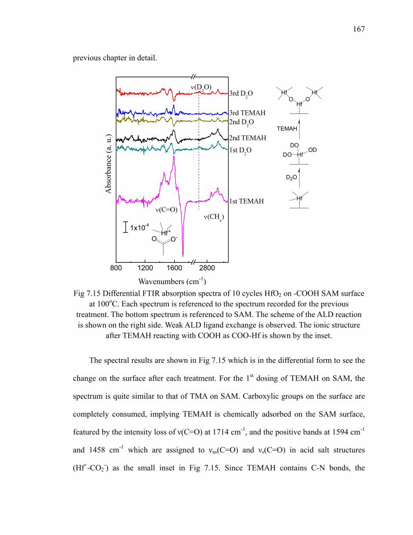
167
previous chapter in detail.
800 1200 1600 2800
3rd D2O
3rd TEMAH2nd D
2O
2nd TEMAH
1st D2O
1st TEMAH
ν(D2O)
ν(CHx)
1x10⁻⁴
ν(C=O)
Fig 7.15 Differential FTIR absorption spectra of 10 cycles HfO2 on -COOH SAM surface at 100oC. Each spectrum is referenced to the spectrum recorded for the previous
treatment. The bottom spectrum is referenced to SAM. The scheme of the ALD reaction is shown on the right side. Weak ALD ligand exchange is observed. The ionic structure
after TEMAH reacting with COOH as COO-Hf is shown by the inset.
The spectral results are shown in Fig 7.15 which is in the differential form to see the
change on the surface after each treatment. For the 1st dosing of TEMAH on SAM, the
spectrum is quite similar to that of TMA on SAM. Carboxylic groups on the surface are
completely consumed, implying TEMAH is chemically adsorbed on the SAM surface,
featured by the intensity loss of ν(C=O) at 1714 cm-1, and the positive bands at 1594 cm-1
and 1458 cm-1 which are assigned to νas(C=O) and νs(C=O) in acid salt structures
(Hf+-CO2-) as the small inset in Fig 7.15. Since TEMAH contains C-N bonds, the
O O-Hf+
Hf
D2O
Hf
Hf
TEMAH
O OHf Hf
ODDO
DO
Wavenumbers (cm-1)
Abs
orba
nce
(a. u
.)
168
broadening of νas/νs(C=O) modes is caused by other C, N and O related modes. The
intensity increase of ν(CHx) around 2800-3000 cm-1 is attributed to the precursor ligand
as well. These bands further confirm that Hf with attached ligands is chemically adsorbed
to the SAM surface. Different from TEMAH directly exposed to H/Si, there is no
interfacial Hf-O-Si mode observed. Therefore, all ALD reactions are limited to the top
surface of the -COOH functionalized SAM.
Upon the subsequent D2O exposure, there is a positive band for ν(CHx) at
2800-3000 cm-1, which is abnormal because the Hf precursor should be hydrolyzed by
D2O and the ligand should be replaced by -OD. It could be caused by perturbed
underlying -CH2 chains since the bands are mainly of νs/νas(CH2). The possibility of
ligand from hydrolyzed residue TEMAH in the chamber adsorbed to the surface cannot
be excluded. The reversible intensity fluctuation of the bands at 1476 and 1581 cm-1 is
related to the ν(C=O) shift induced by the change of C=O bond environment in the
interfacial (CO2-)-Hf+ as the Al2O3 case. In addition, the D2O incorporation is observed
by -OD stretching mode at 2707 cm-1 as the evidence of ALD ligand exchange. The
reaction scheme is shown on the right side of Fig 7.15. The following cycles repeat the
same scheme: after TEMAH exposures, Hf-ligand is adsorbed on the surface; after D2O
exposures, the chemically adsorbed precursor is reacted to form HfO2,
The spectra in Fig 7.16 are referenced to the SAM surface to show the evolution of
HfO2 film with number of cycles. HfO2 phonon mode is observed as a broad band
centered at ~680 cm-1, implying the formation of continuous HfO2 film. It can be seen
that ν(D2O) (2707 cm-1) intensity keeps increasing with the increased number of cycles,
indicating trapped D2O in the film. By ν(CHx) around 2800-3000 cm-1, it can be
concluded that some carbon impurities from ligands remain inside HfO2. Absence of Si-O
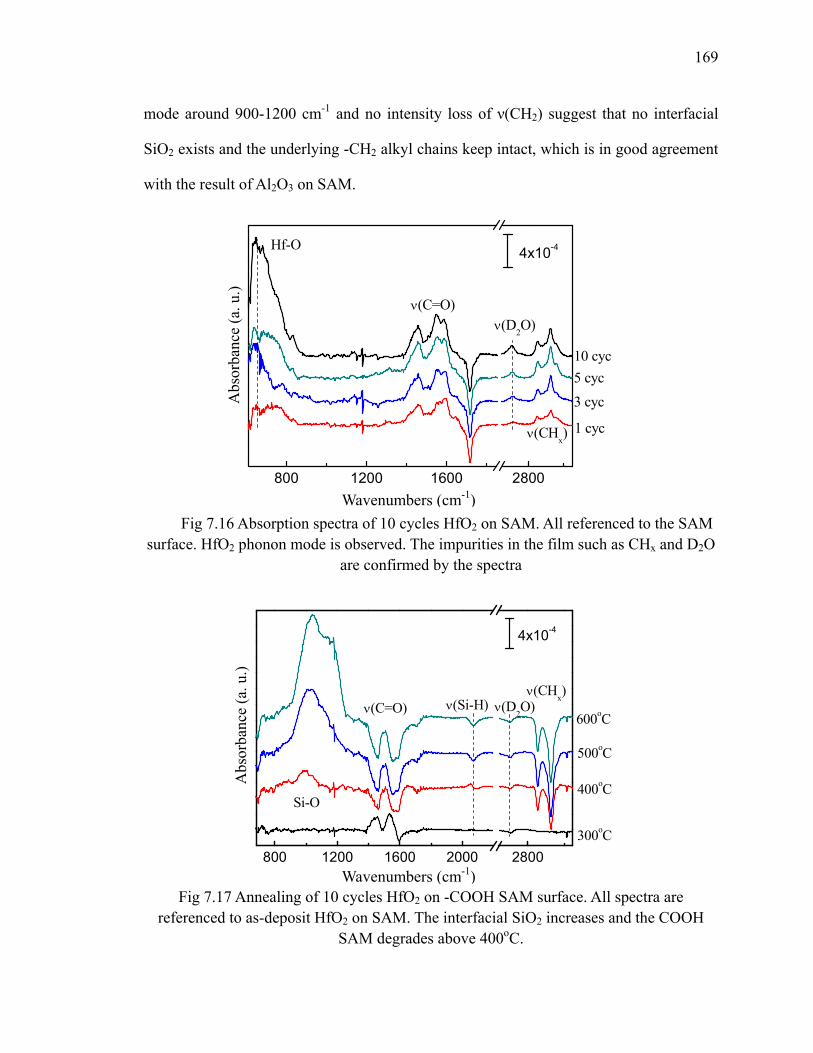
169
mode around 900-1200 cm-1 and no intensity loss of ν(CH2) suggest that no interfacial
SiO2 exists and the underlying -CH2 alkyl chains keep intact, which is in good agreement
with the result of Al2O3 on SAM.
800 1200 1600 2800
10 cyc5 cyc3 cyc
Hf-O
4x10⁻⁴
ν(CHx)
ν(D2O)ν(C=O)
1 cyc
Fig 7.16 Absorption spectra of 10 cycles HfO2 on SAM. All referenced to the SAM surface. HfO2 phonon mode is observed. The impurities in the film such as CHx and D2O
are confirmed by the spectra
800 1200 1600 2000 2800
600oC
500oC
400oC
300oC
Si-O
ν(Si-H)
4x10⁻⁴
ν(C=O) ν(D2O)ν(CHx)
Fig 7.17 Annealing of 10 cycles HfO2 on -COOH SAM surface. All spectra are
referenced to as-deposit HfO2 on SAM. The interfacial SiO2 increases and the COOH SAM degrades above 400oC.
Wavenumbers (cm-1)
Abs
orba
nce
(a. u
.)
Wavenumbers (cm-1)
Abs
orba
nce
(a. u
.)
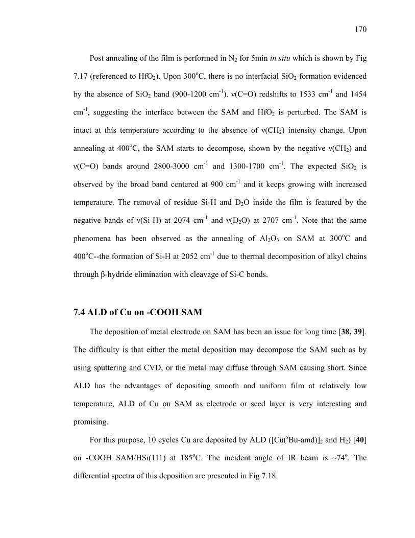
170
Post annealing of the film is performed in N2 for 5min in situ which is shown by Fig
7.17 (referenced to HfO2). Upon 300oC, there is no interfacial SiO2 formation evidenced
by the absence of SiO2 band (900-1200 cm-1). ν(C=O) redshifts to 1533 cm-1 and 1454
cm-1, suggesting the interface between the SAM and HfO2 is perturbed. The SAM is
intact at this temperature according to the absence of ν(CH2) intensity change. Upon
annealing at 400oC, the SAM starts to decompose, shown by the negative ν(CH2) and
ν(C=O) bands around 2800-3000 cm-1 and 1300-1700 cm-1. The expected SiO2 is
observed by the broad band centered at 900 cm-1 and it keeps growing with increased
temperature. The removal of residue Si-H and D2O inside the film is featured by the
negative bands of ν(Si-H) at 2074 cm-1 and ν(D2O) at 2707 cm-1. Note that the same
phenomena has been observed as the annealing of Al2O3 on SAM at 300oC and
400oC--the formation of Si-H at 2052 cm-1 due to thermal decomposition of alkyl chains
through β-hydride elimination with cleavage of Si-C bonds.
7.4 ALD of Cu on -COOH SAM
The deposition of metal electrode on SAM has been an issue for long time [38, 39].
The difficulty is that either the metal deposition may decompose the SAM such as by
using sputtering and CVD, or the metal may diffuse through SAM causing short. Since
ALD has the advantages of depositing smooth and uniform film at relatively low
temperature, ALD of Cu on SAM as electrode or seed layer is very interesting and
promising.
For this purpose, 10 cycles Cu are deposited by ALD ([Cu(sBu-amd)]2 and H2) [40]
on -COOH SAM/HSi(111) at 185oC. The incident angle of IR beam is ~74o. The
differential spectra of this deposition are presented in Fig 7.18.
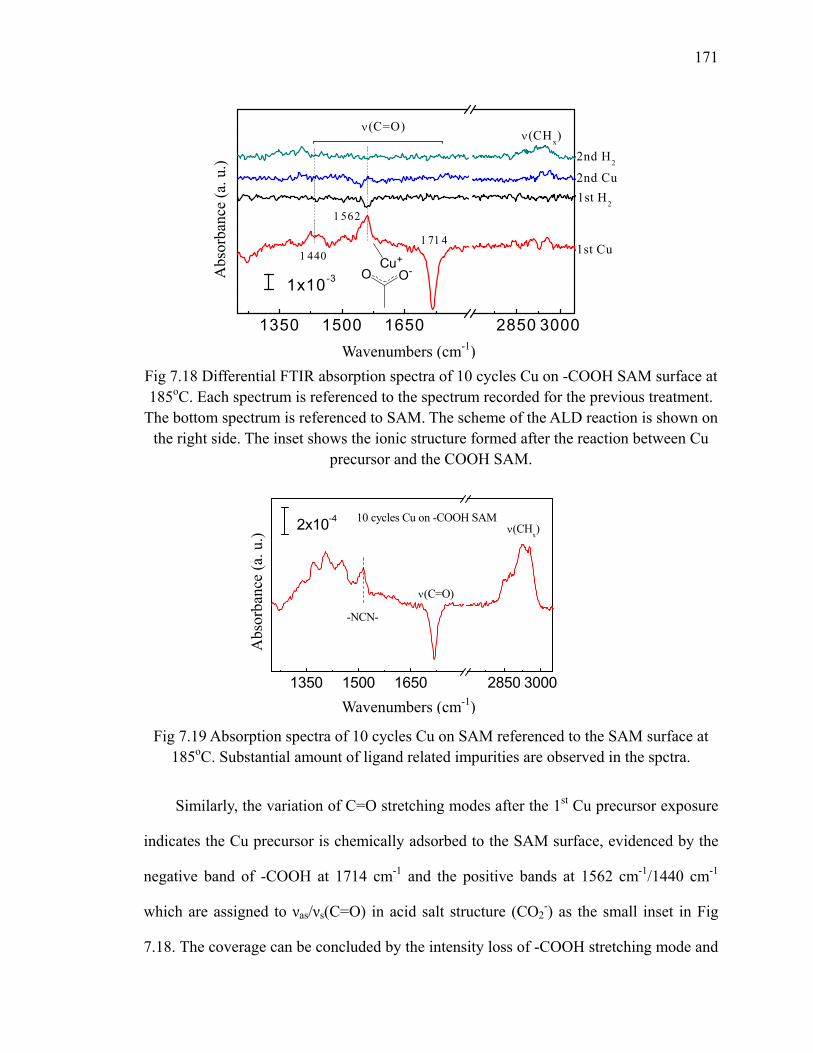
171
1350 1500 1650 2850 3000
17141440
1562
2nd Cu
2nd H2
1st H2
1st Cu
1x10⁻³
ν(CHx)ν(C=O)
Fig 7.18 Differential FTIR absorption spectra of 10 cycles Cu on -COOH SAM surface at 185oC. Each spectrum is referenced to the spectrum recorded for the previous treatment.
The bottom spectrum is referenced to SAM. The scheme of the ALD reaction is shown on the right side. The inset shows the ionic structure formed after the reaction between Cu
precursor and the COOH SAM.
Fig 7.19 Absorption spectra of 10 cycles Cu on SAM referenced to the SAM surface at
185oC. Substantial amount of ligand related impurities are observed in the spctra.
Similarly, the variation of C=O stretching modes after the 1st Cu precursor exposure
indicates the Cu precursor is chemically adsorbed to the SAM surface, evidenced by the
negative band of -COOH at 1714 cm-1 and the positive bands at 1562 cm-1/1440 cm-1
which are assigned to νas/νs(C=O) in acid salt structure (CO2-) as the small inset in Fig
7.18. The coverage can be concluded by the intensity loss of -COOH stretching mode and
O O-Cu+
Wavenumbers (cm-1)
Abs
orba
nce
(a. u
.)
1350 1500 1650 2850 3000
10 cycles Cu on -COOH SAM
ν(C=O)
ν(CHx)2x10⁻⁴
-NCN-
Wavenumbers (cm-1)
Abs
orba
nce
(a. u
.)
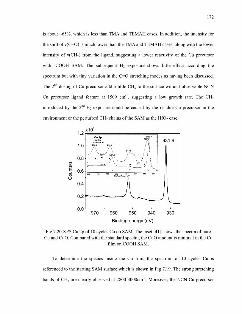
172
is about ~65%, which is less than TMA and TEMAH cases. In addition, the intensity for
the shift of ν(C=O) is much lower than the TMA and TEMAH cases, along with the lower
intensity of ν(CHx) from the ligand, suggesting a lower reactivity of the Cu precursor
with -COOH SAM. The subsequent H2 exposure shows little effect according the
spectrum but with tiny variation in the C=O stretching modes as having been discussed.
The 2nd dosing of Cu precursor add a little CHx to the surface without observable NCN
Cu precursor ligand feature at 1509 cm-1, suggesting a low growth rate. The CHx
introduced by the 2nd H2 exposure could be caused by the residue Cu precursor in the
environment or the perturbed CH2 chains of the SAM as the HfO2 case.
970 960 950 940 9300.0
0.2
0.4
0.6
0.8
1.0
1.2
Cou
nts/
s
Binding energy (eV)
931.9
x104
Fig 7.20 XPS Cu 2p of 10 cycles Cu on SAM. The inset [41] shows the spectra of pure
Cu and CuO. Compared with the standard spectra, the CuO amount is minimal in the Cu film on COOH SAM.
To determine the species inside the Cu film, the spectrum of 10 cycles Cu is
referenced to the starting SAM surface which is shown in Fig 7.19. The strong stretching
bands of CHx are clearly observed at 2800-3000cm-1. Moreover, the NCN Cu precursor
173
ligand feature appears at 1513 cm-1, indicating the C and N impurities inside the film. The
bands at 1300-1476 cm-1 are related to the C, N and O bonds of impurities inside the film.
No evidence of -CH2 loss indicates that the alkyl chains of the -COOH SAM survive
during the ALD process.
To prove the deposition of the Cu, XPS analysis is carried out and Fig 7.20 shows
the Cu 2p spectrum. The Cu 2p1/2 at 931.9 eV [42], compared with the pure Cu and CuO
in the inset of Fig 7.20, can be either Cu0 or Cu1+ but believed to be Cu0 according to the
conductivity study done by Gordon’s group [40]. The small satellite peak resulting from
Cu2+ around 945 eV could be caused by the interfacial (CO2)-Cu bond or trace amount of
CuO.
7.5 Summary
In this chapter, two types of SAMs on H/Si(111) have been discussed: one with
chemically unreactive functional group -CH3 which is CH3-(CH2)17-H/Si(111), and the
other with chemically reactive functional group -COOH which is COOH-(CH2)10
-H/Si(111). The -COOH type SAM is achieved without any Si-O or Si-O-C bond but the
-CH3 type SAM has trace amount of SiO2 at the interface.
The stability of those two SAMs under thermal annealing and ozone exposure is
investigated. The -COOH SAM has higher stability for both cases. The carboxylic head
group survives without substantial decomposition up to 200oC for thermal annealing and
100oC for ozone exposure. In both situations, the deterioration of the carboxylic head
group starts first, and the -CH2 chains decompose at a higher temperature. The -CH3
SAM decomposes above 150oC for annealing and degrades immediately upon ozone
exposure at 60oC. Thus, -COOH SAM shows better quality.
174
ALD of Al2O3, HfO2 and Cu are deposited on -COOH SAM surface. By using in
situ FTIR, the reaction mechanism is studied. All the reactions start from the interaction
between the precursor and -COOH groups by forming (CO2)-metal salt structure.
For Al2O3 deposition on -COOH SAM at 100oC, both TMA/D2O and TMA/ozone
are used. For TMA/D2O, the quality of Al2O3 on SAM is similar to that on SiO2. No
interfacial SiO2 is observed and little ALD incubation period is detected, but D2O
impurity is observable inside the film. The SAM remains intact during the ALD process.
The post annealing result shows the decomposition of the SAM above 300oC. For
TMA/ozone, substantial amount of C-O/C=O impurities are found inside the film due to
the decomposition of the underlying SAM and TMA ligands. Its growth rate is about 1/4
of that of water based ALD. Small amount of Si-O is observed by FTIR.
HfO2 is deposited by TEMAH/D2O on -COOH SAM at 100oC. Similarly, no
interfacial SiO2 is observed during the deposition and the underlying SAM is intact.
However, D2O is incorporated inside the film. The post annealing shows that coated
SAM is stable up to 300oC. Above this temperature, SiO2 keeps growing with the
increased temperature.
Finally, ALD of pure copper on -COOH SAM is demonstrated. It is concluded that
the growth rate is low by the intensity of ligand related modes. Residue NCN ligand
related carbon impurities are detected inside the film. The alkyl chains survive during the
deposition of Cu and XPS Cu 2p spectrum confirms the existence of copper film.
Bibliography 1. J. J. Gooding, F. Mearns, W. Yang and J. Liu, Self-assembled monolayers into the
21st century: Recent advances and applications, Electroanalysis 15 (2003), 81. 2. S. Onclin, B. J. Ravoo and D. N. Reinhoudt, Engineering silicon oxide surfaces
175
using self-assembled monolayers, Angew. Chem. Int. Ed. 44 (2005), 6282. 3. F. Schreiber, Structure and growth of self-assembling monolayers, Progress in
Surface Science 65 (2000), 151. 4. ---, Self-assembled monolayers: From 'simple' model system to biofunctionalized
interfaces, J. Phys.: Condens. Matter 16 (2004), R881. 5. A. Ulman, Formation and structure of self-assembled monolayers, Chem. Rev. 96
(1996), 1533. 6. D. D. M. Wayner and R. A. Wolkow, Organic modification of hydrogen terminated
silicon surfaces, J. Chem. Soc., Perkin Trans. 2 (2002), 23. 7. A. B. Sieval, R. Linke, H. Zuilhof and E. J. R. Sudhölter, High-quality alkyl
monolayers on silicon surfaces, Adv. Mat. 12 (2000), 1457. 8. R. Pool, P. Schapotschnikow and T. J. H. Vlugt, Solvent effects in the adsorption of
alkyl thiols on gold structures: A molecular simulation study J. Phys. Chem. C 111 (2007), 10201.
9. S. R. Wasserman, Y. T. Tao and G. M. Whitesides, Structure and reactivity of alkylsiloxane monolayers formed by reaction of alkyltrichlorosilanes on silicon substrates, Langmuir 5 (1989), 1074.
10. N. A. K. Chaki, M. Aslam, J. Sharma and K. Vijayamohanan, Applications of self-assembled monolayers in materials chemistry, Proc. Indian Acad. Sci. (Chem. Sci.) 113 (2001), 659.
11. R. Chen, H. Kim, P. C. McIntyre, D. W. Porter and S. F. Bent, Achieving area-selective atomic layer deposition on patterned substrates by selective surface modification, Appl. Phys. Lett. 86 (2005), 191910.
12. R. Chen and S. F. Bent, Chemistry for positive pattern transfer using area-selective atomic layer deposition, Adv. Mat. 18 (2006), 1086.
13. O. Seitz, T. Böcking, A. Salomon, J. J. Gooding and D. Cahen, Importance of monolayer quality for interpreting current transport through organic molecules: Alkyls on oxide-free Si, Langmuir 22 (2006), 6915.
14. N. P. Kobayashia, C. L. Donleya, S.-Y. Wanga and R. S. Williamsa, Atomic layer deposition of aluminum oxide on hydrophobic and hydrophilic surfaces Journal of Crystal Growth 299 (2007), 218.
15. A. B. Sieval, B. v. d. Hout, H. Zuilhof and E. J. R. Sudhölter, Molecular modeling of covalently attached alkyl monolayers on the hydrogen-terminated Si(111) surface, Langmuir 17 (2001), 2172.
16. D. M. Byler, W. V. Gerasimowicz, H. Susi and M. Schnitzer, FT-IR spectra of soil constituents: Fulvic acid and fulvic acid complex with ferric ions, Appllied Spectroscopy 41 (1987), 1428.
17. R. Boukherroub, J. T. C. Wojtyk, D. D. M. Wayner and D. J. Lockwood, Thermal hydrosilylation of undecylenic acid with porous silicon, J. Electrochem. Soc. 149 (2002), H59.
18. H. Asanuma, G. P. Lopinsk and H.-Z. Yu, Kinetic control of the photochemical
176
reactivity of hydrogen-terminated silicon with bifunctional molecules, Langmuir 21 (2005), 5013.
19. R. T. Conley, Infrared spectroscopy, Allyn and Bacon, Inc. (1972). 20. O. Gershevitz and C. N. Sukenik, In situ FTIR-ATR analysis and titration of
carboxylic acid-terminated sams, J. Am. Chem. Soc 126 (2003), 482. 21. R. G. Snyder, H. L. Strauss and C. A. Elliger, Carbon-hydrogen stretching modes and
the structure of n-alkyl chains. 1. Long, disordered chains, J. Phys. Chem 86, 5145 - 5150.
22. M. D. Porter, T. B. Bright, D. L. Allara and C. E. D. Chidseyi, Spontaneously organized molecular assemblies. 4. Structural characterization of n-alkyl thiol monolayers on gold by optical ellipsometry, infrared spectroscopy, and electrochemistry, J. Am. Chem. Soc. 109 (1987), 3559-3568.
23. S. Lenfant, D. Guerin, F. TranVan, C. Chevrot, S. Palacin, J. P. Bourgoin, O. Bouloussa, F. Rondelez and D. Vuillaume, Electron transport through rectifying self-assembled monolayer diodes on silicon: Fermi level pinning at the molecule-metal interface, J. Phys. Chem. B (2006), 13947.
24. A. Faucheux, F. Yang, P. Allongue, C. H. d. Villeneuve, F. Ozanam and J.-N. Chazalviel, Thermal decomposition of alkyl monolayers covalently grafted on (111) silicon, Appl. Phys. Lett. 88 (2006), 193123.
25. M. M. Sung, G. J. Kluth, O. W. Yauw and R. Maboudian, Thermal behavior of alkyl monolayers on silicon surfaces, Langmuir 13 (1997), 6164.
26. K. T. Queeney, N. Herbots, J. M. Shaw, V. Atluri and Y. J. Chabal, Infrared spectroscopic analysis of an ordered Si/SiO2 interface, Appl. Phys. Lett. 84 (2004), 493.
27. A. Faucheux, A. C. Gouget-Laemmel, C. H. d. Villeneuve, R. Boukherroub, F. Ozanam, P. Allongue and e.-N. Chazalviel, Well-defined carboxyl-terminated alkyl monolayers grafted onto H-Si(111): Packing density from a combined AFM and quantitative IR study, Langmuir 22 (2006), 153.
28. M. M. Frank, Y. J. Chabal and G. D. Wilk, Nucleation and interface formation mechanisms in atomic layer deposition of gate oxides, Appl. Phys. Lett. 82 (2003), 4758.
29. M. M. Frank, Y. J. Chabal, M. L. Green, A. Delabie, B. Brijs, G. D. Wilk, M. Y. Ho, E. B. O. d. Rosa, I. J. R. Baumvol and F. C. Stedile, Enhanced initial growth of atomic-layer-deposited metal oxides on hydrogen-terminated silicon, 83 (2003), 740.
30. J. D. Ferguson, A. W. Weimer and S. M. George, Atomic layer deposition of Al2O3 films on polyethylene particles, Chem. Mat. 16 (2004), 5602.
31. T. R. Gow, R. Lin, L. A. Cadwell, F. Lee, A. L. Backman and R. I. Masel, Decomposition of trimethylaluminum on silicon(100), Chem. Mat. 1 (1989), 406.
32. A. W. Ott, J. W. Klaus, J. M. Johnson and S. M. George, Al2o3 thin film growth on Si(100) using binary reaction sequence chemistry, Thin Solid Film 292 (1997), 135.
177
33. W. Mozgawa, M. Sitarz and M. Rokita, Spectroscopic studies of different aluminosilicate structures, Journal of Molecular Structure 512 (1999), 251.
34. A. Fidelis, F. Ozanam and J.-N. Chazalviel, Fully methylated, atomically flat (111) silicon surface, Surf. Sci. 44 (2000), L7.
35. M.-T. Ho, Y. Wang, R. T. Brewer, L. S. Wielunski and Y. J. Chabal, In situ infrared spectroscopy of hafnium oxide growth on hydrogen-terminated silicon surfaces by atomic layer deposition, Appl. Phys. Lett. 87 (2005), 133103.
36. X. Liu, S. Ramanathan, A. Longdergan, A. Srivastava, E. Lee, T. E. Seidel, J. T. Barton, b. Dawen Pang and R. G. Gordonb, ALD of hafnium oxide thin films from tetrakis(ethylmethylamino) hafnium and ozone, J. Electrochem. Soc. (2005), 2005.
37. J. Kwon, M. Dai, M. D. Halls and Y. J. Chabal, Detection of a formate surface intermediate in the atomic layer deposition of high-κ dielectrics using ozone, Chem. Mat. 20 (2008), 3248.
38. B. d. Boer, A. Hadipour, M. M. Mandoc, T. v. Woudenbergh and P. W. M. Blom, Tuning of metal work functions with self-assembled monolayers, Advanced Materials 17 (2005), no. 5, 621-625.
39. B. d. Boer, H. Meng, D. F. Perepichka, J. Zheng, M. M. Frank, Y. J. Chabal and Z. N. Bao, Synthesis and characterization of conjugated mono- and dithiol oligomers and characterization of their self-assembled monolayers, Langmuir 19 (2003), 4272.
40. Z. Li, A. Rahtu and R. G. Gordon, Atomic layer deposition of ultrathin copper metal films from a liquid copper(I) amidinate precursor, Journal of Electrochemical Society 153 (2006), C787-C794.
41. http://www.lasurface.com/database/spectrexps.php. 42. J. F. Moulder, N. F. Stickle, P. E. Sobol and K. D. B. I. J. Chastain, Handbook of
X-ray photoelectron spectroscopy, Perkin-Elmer Corporation (1995).

178
Chapter 8: Summary
The main contribution of the work described in this thesis is the fundamental
understanding of the ALD process for a variety of important systems, derived from in-situ
FTIR studies. This technique was essential to characterize the properties of both starting
surfaces and precursors, and to study the essential elements of ALD. The mechanistic
aspects of ALD are investigated including the side reactions taking place during ALD
growth, which provides the necessary insight to suggest possible optimization schemes
for future ALD applications, as summarized below.
1) Two types of starting surfaces are discussed in detail: nitrided Si surface and
SAMs modified H/Si surface. In this dissertation, SiNx is used as an oxygen barrier to
suppress interfacial SiO2 for ALD of high-κ metal oxides, and SAMs are for
area-selective ALD. But both have many other applications as well.
For the nitrided surfaces, we studied the mechanism of thermal NH3 nitridation of
flat H/Si(111) surface and vicinal H/Si(111) surfaces including monohydride and
dihydride stepped surfaces. By varying the temperature from 150oC to 600oC at a small
temperature step of 25oC, the surface interaction with NH3 is investigated to conclude the
whole picture of NH3 nitridation. Flat H/Si(111) surface and monohydride stepped
H/Si(111) surface show the same nitridation behavior due to their structural similarity.
The nitridation starts from NH3 dissociation by replacing the surface Si-H with Si-NH2 at
350oC. The nitrogen insertion to Si-Si network and formation of SiNx layer take place
above 400oC. Dihydride stepped H/Si(111) shows a very different nitridation mechanism,
where desorption of Si-H begins at 325oC accompanied by the forming an unexpected
H-Si-NH-Si bridging structure at the step edge. DFT calculation perfectly confirms our
179
vibrational mode assignments and assumed nitridation model. Upon 400oC, nitrogen
insertion to Si-Si back bond is evidenced. Theses information is helpful to determine
condition for initial interaction between NH3 and surface Si-H and we understand how
NH3 attacks the surface and is bonded to the surface. By varying the temperature, the
termination of the Si surface can be changed.
For the SAM-terminated surfaces, the stability of two types of SAMs is studied
including -COOH terminated SAM (reactive) and -CH3 terminated SAM (unreactive)
grafted on H/Si(111) surface via direct Si-C bond. -COOH SAM has higher stability
under thermal annealing in N2 and ozone exposure. The carboxylic head group survives
without substantial decomposition up to 200oC for thermal annealing and 100oC for
ozone exposure, while the CH2 chains decompose at a higher temperature. The -CH3
SAM decomposes above 150oC for annealing and degrades immediately upon ozone
exposure at 60oC. Thus, -COOH SAM shows much better quality and it is a very reactive
surface for ALD which can be utilized for selective growth.
2) ALD of high-κ metal oxides and pure metal are studied, including HfO2, Al2O3,
La2O3 and pure Cu on various surface:
HfO2 is deposited by TEMAH/ozone at 100oC, and it is compared with the
deposition by TEMAH/D2O. On H/Si surface, ozone based HfO2 shows substantial
interfacial Si oxide and carbonyl/nitro derivatives as impurities in the film without
trapped water/OH. By using SiNx and -COOH SAM surfaces, the interfacial SiO2 is
suppressed for ozone based ALD.
Al2O3 is deposited by TMA/ozone on H/Si(111) at 300oC. When excessive ozone
exposure is used, an unpredicted formate surface intermediate is detected and studied
assisted by DFT calculations. Substantial interfacial SiO2 is observed during the ALD

180
process. When the ozone pulse length is shortened, the film quality is improved
evidenced by the absence of formate species and minimal interfacial SiO2 which is
comparable to water based ALD but with lower growth rate. The gas phase reaction of
TMA/D2O is straightforward and CH4/CD4 are the only byproducts, while the reaction of
TMA/ozone is much more complicated. C2H4 is not the only byproduct and the oxidation
of the methyl terminal group/Al-O-CH3 may prevail which needs further study. The
reaction pathway could be determined by ozone amount. By using -COOH SAM surface,
high quality Al2O3 is achieved by TMA/D2O at 100oC without interfacial SiO2 due to the
high reactivity and protection of -COOH SAM.
In short, ozone based ALD can improve the film quality but the reaction is much
more complicated due to ozone’s high reactivity. The amount of ozone significantly alters
the reaction pathway and the film quality. By using SiNx and SAMs surfaces, the surface
properties are modified and interfacial SiO2 is suppressed which are very good starting
surfaces for ALD.
La2O3 is deposited by using a brand new precursor, La(iPr-MeAMD)3, and D2O. By
checking the La precursor gas phase, all ligand features are observed. Partial
hydroxylation of the precursor is detected in the gas phase by the unexpected stretching
vibrational modes resulting from C=N and N-H in free hydrogenated ligands. The gas
phase reaction of La(iPr-MeAMD)3 and D2O confirms this finding. The growth of La2O3
on H/Si(111) surface shows that La(iPr-MeAMD)3 is highly reactive with H/Si and
involves the formation of a Si-O-La bond due to the partially hydrolyzed precursor,
where the free hydrogenated ligand is unreactive with the surface. For the deposition at
200oC, substantial acetate/carbonate impurities are detected, while for the deposition at
300oC, acetate/carbonate impurities are reduced but cyanamide (or carbodiimide)
181
intermediate species are observed with increased interfacial SiO2. The highly hygroscopic
nature of La2O3 results in CVD-like deposition and thickness non-uniformities on a
macroscopic scale. The deposition of LaxAlyO nanolaminate by alternating TMA/D2O
and La(iPr-MeAMD)3/D2O ALD cycles successfully suppresses CVD-like reactions and
minimizes the acetate/carbonate incorporation while remains the high dielectric constant.
Thus, the properties and reactions of the new La precursor are studied in detail. The
intrinsic of La2O3 makes the ALD process difficult. With the understanding of the its
mechanism, the ALD process can be optimized such as by using Al2O3 incorporated
La2O3.
Finally, pure copper is deposited by using a novel liquid copper precursor--copper(I)
di-sec-butylacetamidinate ([Cu(sBu-amd)]2) and molecular hydrogen on SiO2 surface.
The evolution of SiO2 phonon modes in the IR spectra clearly shows the agglomeration
and the diffusion of Cu on/into SiO2 during the initial 10 cycles. Cu agglomeration and
diffusion increase when the deposition temperature is raised. The H2 reduction of the
precursor ligand and ligand hydrogenation are observed by the vibrational modes
attributed to CHx and NCN bonds. Ex situ XPS results confirm the deposition of copper
on the SiO2 surface. Both FTIR and XPS results show residue ligand impurities inside the
Cu film with small amount of N (< 2%) and substantial amount of C for the initial cycles
due to incomplete ALD reactions. RBS indicates that the growth rate on SiO2 is
temperature dependent and the maximum growth rate is found in the range of 185-250oC
based on one ALD cycle. At 185oC, the thickness of 10 cycles Cu is 1.04-1.18 nm with
uniform distribution.
The Cu deposition at 185oC on other surfaces is studied as well, such as H/Si, SiNx,
Al2O3 and SAM surfaces. FTIR and XPS show the similar film contents and growth
182
mechanism as on SiO2. However, much lower growth rate is found for all those surfaces
than that of SiO2 surface. Cu3N is deposited on SiO2 at 160oC successfully. After
annealing at 225oC in forming gas, the Cu3N is partially reduced to Cu with little Cu
agglomeration.
Therefore, the properties and the initial interactions of the new precursor with SiO2
and other surfaces are addressed and Cu agglomeration/diffusion is observed as well for
the initial ALD cycles. This information is critical for the subsequent processes of Cu
ALD. In addition, ALD of metal on SAMs may resolve the problem of making metal
electrode on SAMs as the application for organic devices.
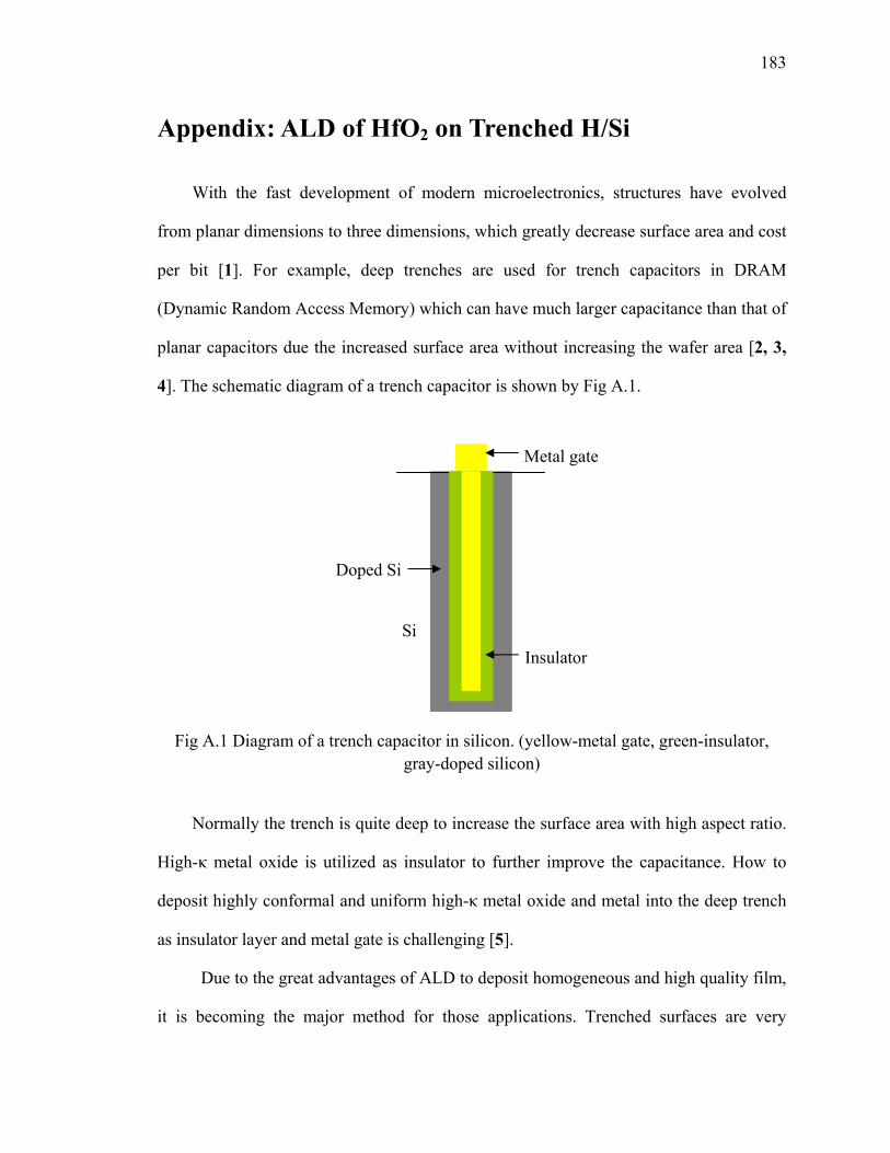
183
Appendix: ALD of HfO2 on Trenched H/Si
With the fast development of modern microelectronics, structures have evolved
from planar dimensions to three dimensions, which greatly decrease surface area and cost
per bit [1]. For example, deep trenches are used for trench capacitors in DRAM
(Dynamic Random Access Memory) which can have much larger capacitance than that of
planar capacitors due the increased surface area without increasing the wafer area [2, 3,
4]. The schematic diagram of a trench capacitor is shown by Fig A.1.
Fig A.1 Diagram of a trench capacitor in silicon. (yellow-metal gate, green-insulator,
gray-doped silicon)
Normally the trench is quite deep to increase the surface area with high aspect ratio.
High-κ metal oxide is utilized as insulator to further improve the capacitance. How to
deposit highly conformal and uniform high-κ metal oxide and metal into the deep trench
as insulator layer and metal gate is challenging [5].
Due to the great advantages of ALD to deposit homogeneous and high quality film,
it is becoming the major method for those applications. Trenched surfaces are very
Si
Doped Si
Insulator
Metal gate
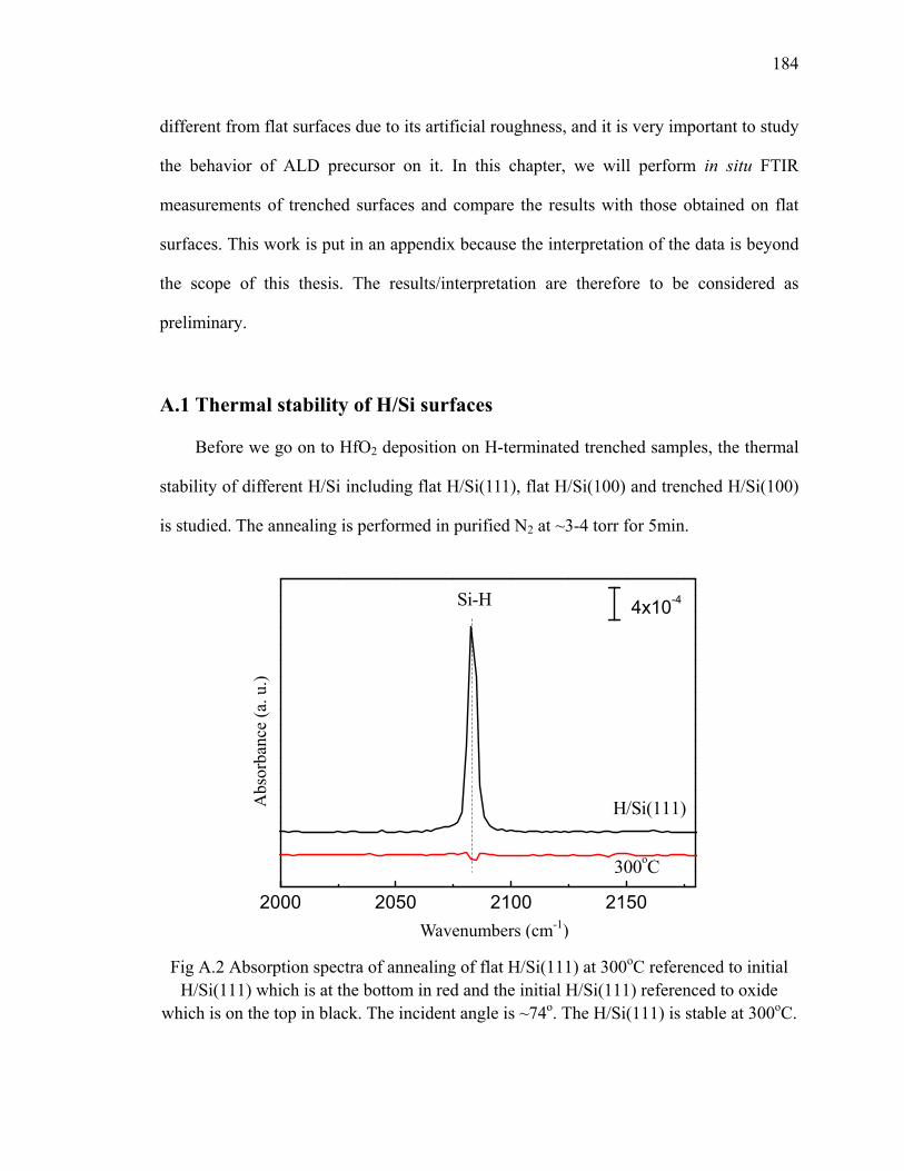
184
different from flat surfaces due to its artificial roughness, and it is very important to study
the behavior of ALD precursor on it. In this chapter, we will perform in situ FTIR
measurements of trenched surfaces and compare the results with those obtained on flat
surfaces. This work is put in an appendix because the interpretation of the data is beyond
the scope of this thesis. The results/interpretation are therefore to be considered as
preliminary.
A.1 Thermal stability of H/Si surfaces
Before we go on to HfO2 deposition on H-terminated trenched samples, the thermal
stability of different H/Si including flat H/Si(111), flat H/Si(100) and trenched H/Si(100)
is studied. The annealing is performed in purified N2 at ~3-4 torr for 5min.
2000 2050 2100 2150
Si-H
300oC
4x10⁻⁴
H/Si(111)
Fig A.2 Absorption spectra of annealing of flat H/Si(111) at 300oC referenced to initial H/Si(111) which is at the bottom in red and the initial H/Si(111) referenced to oxide
which is on the top in black. The incident angle is ~74o. The H/Si(111) is stable at 300oC.
Wavenumbers (cm-1)
Abs
orba
nce
(a. u
.)

185
Annealing of flat H/Si(111) at 300oC is shown in Fig A.2. The black curve is the
initial H/Si(111) spectrum referenced to an oxide surface and the bottom red curve
shows the difference due to annealing, using the initial H/Si(111) as reference. The Si-H
stretching mode is at 2083 cm-1 as discussed in chapter 2 [6]. The single Si-H peak in
the spectrum is due to the monohydride structure on H/Si(111). After annealing at 300oC,
the surface remains almost unchanged (no net loss of integrated area). It can be
concluded that the Si-H is stable at this temperature. Normally Si-H is much more stable
in UHV environment and can survive at higher temperature. Our ALD reactor is not
maintained as UHV environment, thus residue water and other contaminants existing in
the chamber reduce the stability of Si-H.
2000 2200
2142
2100
2110
4x10⁻⁴
2060
400oC
350oC
300oC
250oC200oC150oC
Fig A.3 Absorption spectra of annealing of flat H/Si(100) which is referenced to initial H/Si(100) and the inset is the initial H/Si(100) which is reference to oxide surface. The
incident angle is ~74o. The surface is stable up to 250oC
2000 2100 2200
H/Si(100)
2139
21031x10-4
2088
Wavenumbers (cm-1)
Abs
orba
nce
(a. u
.)
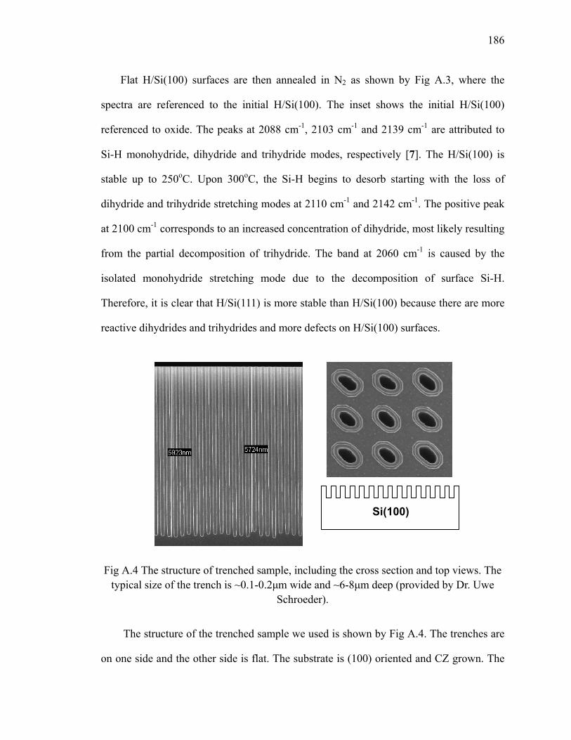
186
Flat H/Si(100) surfaces are then annealed in N2 as shown by Fig A.3, where the
spectra are referenced to the initial H/Si(100). The inset shows the initial H/Si(100)
referenced to oxide. The peaks at 2088 cm-1, 2103 cm-1 and 2139 cm-1 are attributed to
Si-H monohydride, dihydride and trihydride modes, respectively [7]. The H/Si(100) is
stable up to 250oC. Upon 300oC, the Si-H begins to desorb starting with the loss of
dihydride and trihydride stretching modes at 2110 cm-1 and 2142 cm-1. The positive peak
at 2100 cm-1 corresponds to an increased concentration of dihydride, most likely resulting
from the partial decomposition of trihydride. The band at 2060 cm-1 is caused by the
isolated monohydride stretching mode due to the decomposition of surface Si-H.
Therefore, it is clear that H/Si(111) is more stable than H/Si(100) because there are more
reactive dihydrides and trihydrides and more defects on H/Si(100) surfaces.
Fig A.4 The structure of trenched sample, including the cross section and top views. The
typical size of the trench is ~0.1-0.2μm wide and ~6-8μm deep (provided by Dr. Uwe Schroeder).
The structure of the trenched sample we used is shown by Fig A.4. The trenches are
on one side and the other side is flat. The substrate is (100) oriented and CZ grown. The
Si(100)
187
typical size of the trenches is ~0.1-0.2μm wide and ~6-8μm deep. The surface is
artificially rough. The hydrogen-terminated trenched Si(100) is measured by IR with the
IR facing the trenched side, as the inset in Fig A.5. The spectrum is presented in Fig A.5
which is taken at normal incidence. The stretching modes of Si-H are around 2100 cm-1
and the bending mode of Si-H are observed ~620 cm-1. The broad negative band at
900-1300 cm-1 corresponds to SiO2 TO/LO modes due to the etching of HF [8].
Note that to fully remove the SiO2, 10 min HF etching is used in this case. The
prolonged etching time will not rough the surface once the surface is fully passivated by
hydrogen [9]. As in the inset of Fig A.5, three strong modes are observed at 2087 cm-1,
2104 cm-1 and 2139 cm-1, which are tentatively assigned to monohydride, dihydride and
trihydride modes. Due to the roughness of the surface, more coupled modes may appear
and overlap within this range. The spectrum taking at ~74o shows little difference from
that of normal incidence resulting from the surface roughness. So it can be concluded that
trenches dominate the contribution.
The sine-wave like baseline oscillation in Fig A.5 is caused by the trenched surface
[10]. There is an interference due to the change of index of refraction between the trench
area and the solid Si region. The oscillation frequency depends on the depth of the
trenches. The effective refractive index of the surface is related to the trench top width
since the increased top void fraction will make it closer to that of the air lowering the
reflectivity. Although an accurate model is difficult, we use a highly simplified mode
according to Fabry-Pérot interferometer [11]:
θ
λλ
cos2
20
nd≈Δ Eq A.1
where n is the refractive index, d is the trench depth and n≈nSi=4, to get an estimate of the

188
trench depth and find that d is around 1-5μm.
1000 1500 2000 2500 3000 3500 4000
Si-Oν(Si-H)
5x10⁻³δ(Si-H)
Fig A.5 The absorption spectrum of hydrogen terminated trenched Si(100). The inset
shows the magnified Si-H stretches. The incident angle of IR is ~0o. The curved baseline is due to the trenches. And the small schematic shows the IR transmission geometry.
Thermal annealing is carried on for H-terminated trenched Si as well with the same
condition. The spectral results are shown in Fig A.6. Upon 250oC, the surface Si-H starts
to decompose featured by the negative bands corresponded to monohydride, dihydride
and trihydride stretches which are centered at 2085 cm-1, 2108 cm-1, and 2137 cm-1,
respectively. The band appearing at 2061 cm-1 is due to the decoupled Si-H resulting from
thermal decomposition. At 350oC, the surface is being oxidized evidenced by the broad
Si-O band center ~998 cm-1. The modes appearing at 2175 cm-1 and 2264 cm-1 are caused
by the oxygen insertion into Si-Si bond. The 2175 cm-1 mode is assigned to Si-H shifted
IR
2000 2100 2200
20872104
1x10-32139
Wavenumbers (cm-1)
Abs
orba
nce
(a. u
.)
189
by insertion of two oxygen atoms (O2-Si-H) and 2262 cm-1 mode is assigned to Si-H
shifted by insertion of three oxygen atoms (O3-Si-H) [12], which are getting stronger with
more Si-O formation.
1000 1200
998450oC
400oC
350oC
300oC250oC200oC
5x10⁻³
150oC
2000 2400
21752264
21372108
Si-H
Ox-Si-HSi-O
1x10⁻³
20612085
Fig A.6 Absorption spectra of annealing of H-terminated trenched Si surface which are referenced to H/Si. The surface is not as stable as the flat surface and Si-H starts to
desorb from the surface upon 250oC annealing.
By comparing above results, it is found that H/Si(111) is the most stable surface and
remains unchanged at 300oC annealing. Due to the presence of more defects,
H-terminated trenched Si(100) is the least stable surface and its Si-H decomposes at
250oC while flat H/Si(100) is stable up to 250oC. However, when the ALD reactor is
contaminated such as by large amount of residue metal precursor and hydroxyl group, the
stability of H/Si will be further decreased.
Wavenumbers (cm-1)
Abs
orba
nce
(a. u
.)
190
A.2 HfO2 deposition on trenched H/Si(100)
Based on the thermal stability study of H/Si we have discussed above, HfO2 is
deposited on them by TEMAH and D2O. The comparison of HfO2 deposition on flat
H/Si(100) surface and on trenched H/Si(100) will be presented in the following part.
900 2000 2100 2200 2300
ν(Si-H)
θ=74ο
1 dosing of TEMAH on trenched H/Si at 100oC
θ=74ο
2x10⁻⁴
θ=4ο
1950 2100 2250
1x10⁻³
100oCFlat H/Si(100)
Fig A.7 Absorption spectra of trenched H/Si(100) exposed to TEMAH at 100oC which are referenced to H/Si. The bottom spectrum in black is taken at normal incidence and the
top spectrum in red is taken at 74o. The inset shows the spectrum of flat H/Si(100) exposed to TEMAH at 100oC and taken at 74o. The loss of Si-H indicates the interaction.
First the trenched H/Si surface is exposed to TEMAH at 100oC as shown by the
spectra in Fig A.7 which are referenced to H/Si and show the range of Si-H stretching
modes. The spectrum for the trenched sample taken at 74o has a substantial change in the
Si-H stretching modes, indicating the TEMAH is interacting with the surface Si-H and
the flat H/Si(100) exhibits similar feature after TEMAH dosing at 74o (the inset of Fig
A.7).
However, the spectrum of the trenched sample taken at normal incidence only shows
Wavenumbers (cm-1)
Abs
orba
nce
(a. u
.)
191
small changes (Si-H loss less than 2%) in the range of the Si-H stretches. Since the 74o
spectrum gives the information (dipoles vertical and parallel to the surface) of both flat
surface and trenches (the side of the hole), and normal incidence gives mostly the
information (bonds parallel to the surface) of trenches, the spectral results may indicate
that at 100oC, TEMAH precursor doesn’t enter the trenches to have sufficient reaction
with Si-H. But due to the complexity of the surface geometry, it cannot be simply
explained.
1800 2000 2200 2400
ν(Si-H)
300oC
250oC
200oC
150oC
5x10⁻⁴
Fig A.8 Absorption spectra of trenched H/Si(100) exposed to TEMAH at various
temperatures which are referenced to H/Si and taken at normal incidence. Little change is observed at 150oC, and at higher temperature, more Si-H loss is observed.
When the temperature is increased to 200oC, the loss of Si-H becomes more intense
as shown by Fig A.8, where the surface is thermally stable in N2 as studied in the
previous section, possibly indicating that the precursor has sufficient kinetic energy to be
Wavenumbers (cm-1)
Abs
orba
nce
(a. u
.)
192
driven into the trenches. With further increased temperature, although much more loss of
Si-H is observed, the contribution of the precursor interaction cannot be distinguished
from the thermal effect.
600 900 1200 1500 1800 2100 3000
10cyc5cyc
3rd D2O
1st D2O
2nd D2O3rd TEMAH
2nd TEMAH1st D2O1st TEMAH
δs(Si-H)
ν(CHx)ν(Si-H)
Hf-O-Si
Hf-O
1x10⁻³
Fig A.9 Absorption spectra of 10 cycles HfO2 on trenched H/Si(100) at 300oC which are
referenced to H/Si taken at normal incidence. The inset shows 20 cycles HfO2 on flat H/Si(100) at 100oC which is referenced to H/Si and taken at 74o. Small amount of
Hf-O-Si and impurities is observed. Compared to the deposition on flat H/Si, there is no significant difference.
Further, 10-cycle HfO2 is deposited on trenched H/Si(100) at 300oC (Fig A.9). The
inset of Fig A.9 shows the spectrum of 20 cycles HfO2 deposited on flat H/Si(100)
surface at 100oC. Hf-O mode observed ~680 cm-1 indicates the formation of continuous
HfO2 layer. The broad band around 990 cm-1 is due to the interfacial Hf-O-Si bond [13].
Less amount of impurities (C, N and O) for the deposition at 300oC are observed by the
region at 1300-1700 cm-1 than that at 100oC as well as the reduced D2O amount. The
800 120016002000 2800
20cyc HfO2 on flat H/Si(100)
Si-H
Hf-OHf-O-Si
CHx
1x10⁻³
D2O
Wavenumbers (cm-1)
Abs
orba
nce
(a. u
.)
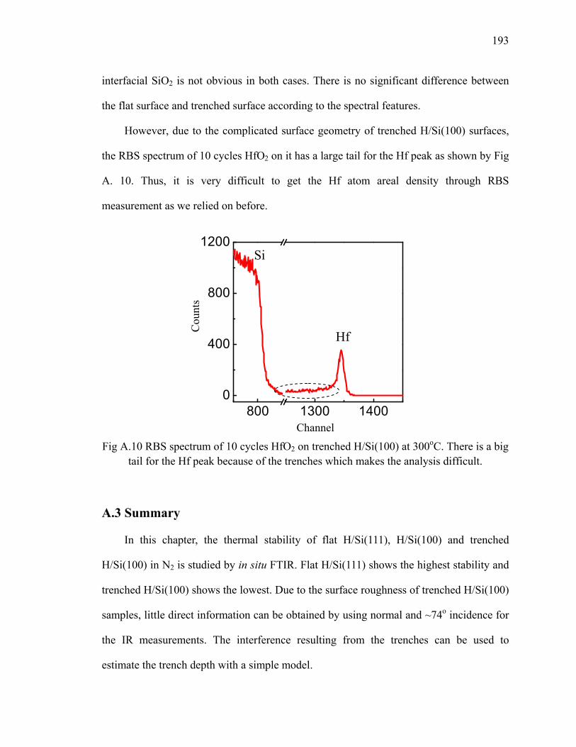
193
interfacial SiO2 is not obvious in both cases. There is no significant difference between
the flat surface and trenched surface according to the spectral features.
However, due to the complicated surface geometry of trenched H/Si(100) surfaces,
the RBS spectrum of 10 cycles HfO2 on it has a large tail for the Hf peak as shown by Fig
A. 10. Thus, it is very difficult to get the Hf atom areal density through RBS
measurement as we relied on before.
800 1300 14000
400
800
1200
Hf
Si
Fig A.10 RBS spectrum of 10 cycles HfO2 on trenched H/Si(100) at 300oC. There is a big tail for the Hf peak because of the trenches which makes the analysis difficult.
A.3 Summary
In this chapter, the thermal stability of flat H/Si(111), H/Si(100) and trenched
H/Si(100) in N2 is studied by in situ FTIR. Flat H/Si(111) shows the highest stability and
trenched H/Si(100) shows the lowest. Due to the surface roughness of trenched H/Si(100)
samples, little direct information can be obtained by using normal and ~74o incidence for
the IR measurements. The interference resulting from the trenches can be used to
estimate the trench depth with a simple model.
Channel
Cou
nts
194
The deposition of HfO2 by using TEMAH and D2O is carried out at various
temperatures. Compared with the deposition on flat H/Si(100), higher temperature (above
200oC) is needed to drive the TEMAH precursor into the trench, as determined from the
results of normal incidence and ~74o IR absorption spectra. The RBS spectrum shows a
large tail resulting from the trenches which makes the analysis difficult. As a result, the
interpretation is only qualitative.
Bibliography 1. A. W. Topol, J. D. C. La Tulipe, L. Shi, D. J. Frank, K. Bernstein, S. E. Steen, A. Kumar, G. U. Singco, A. M. Young, K. W. Guarini and M. Ieong, Three-dimensional integrated circuits, IBM Journal of Research and Development 50 (2006), 491. 2. K. Yamada, K. Yamabe, Tsunashima, Y. Imai, K. Kashio and H. T. Tango, A deep-trenched capacitor technology for 4 mega bit dynamic RAM, Elect. Dev. Meeting 31 (1985), 702. 3. J. Lutzen, A. Birner, M. Goldbach and e. al., Integration of capacitor for sub-100-nm DRAM trench technology, VLSI Technology, 2002. Digest of Technical Papers. 2002 Symposium on (2002), 178. 4. E. Gerritsena, N. Emonetb, C. Caillatb, N. Jourdanb, M. Piazzab, D. Frabouletd, B. Boeckc, A. Berthelota, t. Smitha and P. Mazoyerb, Evolution of materials technology for stacked-capacitors in 65 nm embedded-DRAM Solid-State Electronics 49 (2005), 1767. 5. L. Pinzellia, M. Gros-Jeana, Y. Bréchetb, F. Volpib, A. Bajoleta and J.-C. Giraudina, High-k dielectric deposition in 3D architectures: The case of Ta2O5 deposited with metal–organic precursor TBTDET Microelectronics Reliability 47 (2007), 700. 6. P. Dumas, Y. J. Chabal and G. S. Higashi, Coupling of an adsorbate vibration to a substrate surface phonon: H on Si(111), Physical Review Letters 65 (1990), 1124. 7. Y. J. Chabal, G. S. Higashi, K. Raghavachari and V. A. Burrows, Infrared spectroscopy of Si(111) and Si(100) surfaces after HF treatment: Hydrogen termination and surface morphology, J. Vac. Sci. Technol. A 7(3) (1989), 2104. 8. K. T. Queeney, Y. J. Chabal, M. K. Weldon and K. Raghavachari, Silicon oxidation and ultra-thin oxide formation on silicon studied by infrared absorption spectroscopy, Phys. Stat. Sol. (a) 175 (1999), 77. 9. G. W. Trucks, K. Raghavachari, G. S. Higashi and Y. J. Chabal, Mechanism of HF etching of silicon surface: A theoretical understanding of hydrogen passivation, Phys. Rev. Lett. 65 (1990), no. 4, 504. 10. P. Weidner, A. Kasic, T. Hingst and T. Lindner, Deep trench metrology challenges for
195
75nm DRAM technology, Semiconductor Fabtech (2006), no. Edition 32, Wafer Processing, 115. 11. E. Hecht, Optics (Addison-Wesley series in physics), Addison Wesley (1987). 12. X. Zhang, Y. J. Chabal, S. B. Christman, E. E. Chaban and E. Garfunkel, Oxidation of H-covered flat and vicinal Si(111)-1x1 surfaces, J. Vac. Sci. Technol. A 19(4) (2000), 1725. 13. M.-T. Ho, Y. Wang, R. T. Brewer, L. S. Wielunski and Y. J. Chabal, In situ infrared spectroscopy of hafnium oxide growth on hydrogen-terminated silicon surfaces by atomic layer deposition, Appl. Phys. Lett. 87 (2005), 133103.
196
Acknowledgment of Previous Publications
1. Atomic Layer Deposition of Aluminum Oxide on Carboxylic Acid-terminated Self -Assembled Monolayers M. Li, M. Dai, and Y. J. Chabal Submitted to Appl. Phys. Lett. 2. In-situ Infrared Characterization during Atomic Layer Deposition of Lanthanum Oxide Jinhee Kwon, Min Dai, Mathew D. Halls, Yves J. Chabal and Roy G. Gordon Submitted to J. Phys. Chem. 3. Detection of a Formate Surface Intermediate in the Atomic Layer Deposition of High-K Dielectrics Using Ozone Jinhee Kwon, Min Dai, Mathew D. Halls, and Yves J. Chabal Chem. Mater., 20, 3248-3250, 2008 4. In-situ FTIR Study of Atomic Layer Deposition (ALD) of Copper Metal Films Dai, Min; Kwon, Jinhee; Langereis, Erik; Wielunski, Leszek; Chabal, Yves J.; Li, Zhengwen; Gordon, Roy G. ECS Transactions, 11, 91-101, 2007 5. In-situ Infrared Absorption Monitoring of Atomic Layer Deposition of Metal Oxides on Functionalized Si and Ge Surfaces Min Dai, Jinhee Kwon, Ming-Tsung Ho, Yu Wang, Sandrine Rivillon, Meng Li, Yves Jean Chabal, Marek Boleslawski Mater. Res. Soc. Symp. Proc., 996E, 0996-H07-04, 2007 6. Infrared Characterization of Hafnium oxide grown by Atomic Layer Deposition using Ozone as the oxygen precursor Y. Wang, M. Dai, M-T. Ho, L.S. Wielunski, and Y. J. Chabal Applied Physics Letter, 90, 022906, 2007 7. In-situ Infrared Absorption Spectroscopy for Thin Film Growth by Atomic Layer Deposition Y. Wang, M. Dai, S. Rivillon, M-T. Ho, and Y.J. Chabal SPIE Proceedings, p.63250G, 2006
197
Curriculum Vita
Min Dai Educations
Ph. D in Physics (Surface Science) 2004. 9-2008. 10 Department of Physics, Rutgers University Master of Science in Microelectronics and Solid State Electronics
2001. 9-2004. 6
Department of Physics, Nanjing University, P. R. China Bachelor of Science in Microelectronics and Solid State Electronics
1997. 9-2001. 6
Department of Physics, Nanjing University, P. R. China
Research Experiences (Research Assistant) 2005-Present Mechanistic study of Atomic Layer Deposition (ALD) of
High-κ materials and metals Advisor: Prof. Yves J. Chabal, Rutgers University 2000-2004 Fabrication, characterization and electrical properties of nano-
crystalline silicon (nc-Si) Advisor: Prof. Kunji Chen and Prof. Xinfan Huang, Nanjing University,
P. R. China
Publications 1. Atomic Layer Deposition of Aluminum Oxide on Carboxylic Acid-terminated Self -Assembled Monolayers M. Li, M. Dai, and Y. J. Chabal Submitted to Appl. Phys. Lett. 2. In-situ Infrared Characterization during Atomic Layer Deposition of Lanthanum Oxide Jinhee Kwon, Min Dai, Mathew D. Halls, Yves J. Chabal and Roy G. Gordon Submitted to J. Phys. Chem. 3. Detection of a Formate Surface Intermediate in the Atomic Layer Deposition of High-K Dielectrics Using Ozone Jinhee Kwon, Min Dai, Mathew D. Halls, and Yves J. Chabal Chem. Mater., 20, 3248-3250, 2008 4. In-situ FTIR Study of Atomic Layer Deposition (ALD) of Copper Metal Films Dai, Min; Kwon, Jinhee; Langereis, Erik; Wielunski, Leszek; Chabal, Yves J.; Li, Zhengwen; Gordon, Roy G. ECS Transactions, 11, 91-101, 2007 5. In-situ Infrared Absorption Monitoring of Atomic Layer Deposition of Metal Oxides on Functionalized Si and Ge Surfaces
198
Min Dai, Jinhee Kwon, Ming-Tsung Ho, Yu Wang, Sandrine Rivillon, Meng Li, Yves Jean Chabal, Marek Boleslawski Mater. Res. Soc. Symp. Proc., 996E, 0996-H07-04, 2007 6. Infrared Characterization of Hafnium oxide grown by Atomic Layer Deposition using Ozone as the oxygen precursor Y. Wang, M. Dai, M-T. Ho, L.S. Wielunski, and Y. J. Chabal Applied Physics Letter, 90, 022906, 2007 7. In-situ Infrared Absorption Spectroscopy for Thin Film Growth by Atomic Layer Deposition Y. Wang, M. Dai, S. Rivillon, M-T. Ho, and Y.J. Chabal SPIE Proceedings, p.63250G, 2006 8. Charging and Coulomb blockade effects of the nc-Si embedded in SiNx double-barrier structures Xinfan Huang, Liangcai Wu, Min Dai, Peigao Han, Linwei Yu, Zhongyuan Ma, Yansong Liu, Wei Li, Kunji Chen Journal of Non-Crystalline Solids, 352, 126-1129, 2006 9. Structural characterization and Coulomb blockade of a-SiNx/ nanocrystalline Si/ a-SiNx
asymmetric double-barrier structures L. C. Wu, M. Dai, X. F. Huang, P. G. Han, L. W. Yu, H. C. Zou, W. Li, and K. J. Chen Mater. Res. Soc. Symp. Proc., 832, F3. 6. 1, 2005 10. Collective behavior of single electron effects in a single layer Si quantum dot array at room temperature Linwei Yu, Kunji Chen, Liangcai Wu, Min Dai, Wei Li, Xinfan Huang Physical Review B, 71, 24305, 2005 11.Electronic properties of nanocrystalline-Si embedded in asymmetric ultrathin SiO2 by in-situ fabrication technique L. C. Wu, K. J. Chen, L. W. Yu, M. Dai, Z. Y Ma, P. G. Han, W. Li, X. F. Huang Chinese Physics Letter, 22, 733-736, 2005 12. Formation and charging effect of Si nanocrystals in a-SiNx /a-Si /a-SiNx structures Min Dai, Kai Chen, Xinfan Huang, Liangcai Wu, Lin Zhang, Feng Qiao, Wei Li, Kunji Chen Journal of Applied Physics, 95, 640-645, 2004 13. Room temperature electron tunneling and storing in nanocrystalline silicon floating gate structure Liangcai Wu, Min Dai, Xinfan Huang, Yongjun Zhang, Wei Li, Jun Xu, Kunji Chen Journal of Non-Crystalline Solids, 338-40, 318-321, 2004 14. Size dependent resonant tunneling and storing of electron in nanocrystalline silicon floating gate double-barrier structure Liangcai Wu, Min Dai, Xinfan Huang, Wei Li, Kunji Chen The Journal of Vacuum Science and Technology B,22, 678-681, 2004 15. Room temperature resonant tunneling and Coulomb blockade in nanocrystalline Si with
199
double SiO2 barriers L. C. Wu, K. J. Chen, M. Dai, W. Li, L. W. Yu, X. F. Huang Mat. Res. Soc. Symp. Proc., 794, T3. 42. 1, 2004 16. Charging and Coulomb blockade effects in nanocrystalline Si dots embedded in SiO2
matrix Liangcai Wu, Kunji Chen, Min Dai, Linwei Yu, Peigao Han, Da Zhu, Wei Li, Xinfan Huang Solid-State and Integrated Circuits Technology, Proceedings. 7th International Conference on, 2 (18-21), 898 – 901, 2004 17.A mechanism for the self-organization of colloidal gold nanoparticles Zhang Y J, Han G Q, Li W, Dai M, Zhang Y, Huang X F, Chen K J Chinese Physics Letters, 21, 2486-2488, 2004 18. Capacitance-voltage study of SiO2/nanocrystalline silicon/SiO2 double barrier structures Liangcai Wu, Xinfan Huang, Jianjun Shi, Min Dai, Feng Qiao, Wei Li, Jun Xu, Kunji Chen Thin Solid Film, 425, 221-224, 2003 19. Coulomb blockade effect of carriers in nc-Si embedded in ultrathin SiO2 films Shi Jianjun, Wu Liangcai, Bao Yun, Liu Jiayu, Ma Zhongyuan, Dai Min, Huang Xinfan, Li Wei, Xu Jun, and Kunji Chen. Chinese Journal of Semiconductors, 24, 29-32, 2003 20. New nanocrystalline Si floating gate structure for nonvolatile memory application L. C. Wu, J. J. Shi, K. J. Chen, J. Xu, W. Li, Z. Y. Ma, M. Dai, D. Wu, A.D. Li, X.F. Huang Mat. Res. Soc. Symp. Proc., 737, 2003 21. The charge storage of the nc-Si layer Dai Min, Zhang Lin, Bao Yun, Shi Jian-jun, Chen Kai, Li Wei, Huang Xin-fan and Chen Kun-ji Chinese Physics, 11, 944-947, 2002 22. The charge storage effect of a-SiNx/nc-Si/a-SiNx sandwich structure Dai Min, Bao Yun, Shi Jianjun, Zhang Lin, Li Wei, Chen Kai, Wang Li, Huang Xinfan, Chen Kunji Research & Progress of SSE, 22, 445-448, 2002 (in Chinese)