Embed Size (px)
Citation preview
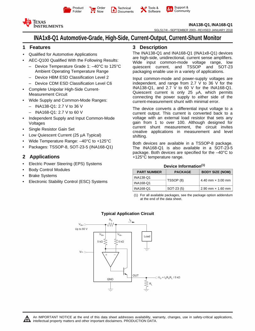
Up to 60 V
IS
VIN+
RS
VIN+ VIN–
5 kΩ 5 kΩ
RL
V = I R R / 5 kΩO S S L
Product
Folder
Order
Now
Technical
Documents
Tools &
Software
Support &Community
An IMPORTANT NOTICE at the end of this data sheet addresses availability, warranty, changes, use in safety-critical applications,intellectual property matters and other important disclaimers. PRODUCTION DATA.
INA138-Q1, INA168-Q1SGLS174I –SEPTEMBER 2003–REVISED JANUARY 2018
INA1x8-Q1 Automotive-Grade, High-Side, Current-Output, Current-Shunt Monitor
1
1 Features1• Qualified for Automotive Applications• AEC-Q100 Qualified With the Following Results:
– Device Temperature Grade 1: –40°C to 125°CAmbient Operating Temperature Range
– Device HBM ESD Classification Level 2– Device CDM ESD Classification Level C6
• Complete Unipolar High-Side Current-Measurement Circuit
• Wide Supply and Common-Mode Ranges:– INA138-Q1: 2.7 V to 36 V– INA168-Q1: 2.7 V to 60 V
• Independent Supply and Input Common-ModeVoltages
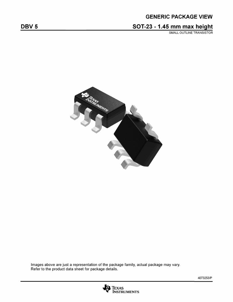
• Single Resistor Gain Set• Low Quiescent Current (25 µA Typical)• Wide Temperature Range: –40°C to +125°C• Packages: TSSOP-8, SOT-23-5 (INA168-Q1)
2 Applications• Electric Power Steering (EPS) Systems• Body Control Modules• Brake Systems• Electronic Stability Control (ESC) Systems
3 DescriptionThe INA138-Q1 and INA168-Q1 (INA1x8-Q1) devicesare high-side, unidirectional, current sense amplifiers.Wide input common-mode voltage range, lowquiescent current, and TSSOP and SOT-23packaging enable use in a variety of applications.
Input common-mode and power-supply voltages areindependent, and range from 2.7 V to 36 V for theINA138-Q1, and 2.7 V to 60 V for the INA168-Q1.Quiescent current is only 25 μA, which permitsconnecting the power supply to either side of thecurrent-measurement shunt with minimal error.
The device converts a differential input voltage to acurrent output. This current is converted back to avoltage with an external load resistor that sets anygain from 1 to over 100. Although designed forcurrent shunt measurement, the circuit invitescreative applications in measurement and levelshifting.
Both devices are available in a TSSOP-8 package.The INA168-Q1 is also available in a SOT-23-5package. Both devices are specified for the –40°C to+125°C temperature range.
Device Information(1)
PART NUMBER PACKAGE BODY SIZE (NOM)INA138-Q1
TSSOP (8) 4.40 mm × 3.00 mmINA168-Q1INA168-Q1 SOT-23 (5) 2.90 mm × 1.60 mm
(1) For all available packages, see the package option addendumat the end of the data sheet.
Typical Application Circuit
2
INA138-Q1, INA168-Q1SGLS174I –SEPTEMBER 2003–REVISED JANUARY 2018 www.ti.com
Product Folder Links: INA138-Q1 INA168-Q1
Submit Documentation Feedback Copyright © 2003–2018, Texas Instruments Incorporated
Table of Contents1 Features .................................................................. 12 Applications ........................................................... 13 Description ............................................................. 14 Revision History..................................................... 25 Pin Configuration and Functions ......................... 46 Specifications......................................................... 5
6.1 Absolute Maximum Ratings ...................................... 56.2 ESD Ratings.............................................................. 56.3 Recommended Operating Conditions....................... 56.4 Thermal Information .................................................. 66.5 Electrical Characteristics........................................... 66.6 Typical Characteristics .............................................. 7
7 Detailed Description .............................................. 97.1 Overview ................................................................... 97.2 Functional Block Diagram ......................................... 97.3 Feature Description................................................. 10
7.4 Device Functional Modes........................................ 108 Application and Implementation ........................ 10
8.1 Application Information............................................ 108.2 Typical Applications ................................................ 12
9 Power Supply Recommendations ...................... 1910 Layout................................................................... 19
10.1 Layout Guidelines ................................................. 1910.2 Layout Example .................................................... 19
11 Device And Documentation Support................. 2011.1 Documentation Support ........................................ 2011.2 Related Links ........................................................ 2011.3 Community Resources.......................................... 2011.4 Trademarks ........................................................... 2011.5 Electrostatic Discharge Caution............................ 2011.6 Glossary ................................................................ 20
12 Mechanical, Packaging, And OrderableInformation ........................................................... 20
4 Revision HistoryNOTE: Page numbers for previous revisions may differ from page numbers in the current version.
Changes from Revision H (May 2016) to Revision I Page
• Changed Thermal Information data for INA168-Q1 DBV device .......................................................................................... 6
Changes from Revision G (January 2014) to Revision H Page
• Changed Application bullets .................................................................................................................................................. 1• Added Device Information, ESD Ratings, Recommended Operating Conditions, and Thermal Information tables,
and Feature Description, Application and Implementation, Power Supply Recommendations, Layout, Device andDocumentation Support, and Mechanical, Packaging, and Orderable Information sections ................................................. 1
• Added new automotive qualification features bullet, and deleted old bullet........................................................................... 1• Added pin names to all figures and removed all pin numbers ............................................................................................... 1• Deleted Ordering Information table; information available in the Package Option Addendum at the end of this data sheet 4• Added missing minus sign to VIN– pin in pin configuration figures ......................................................................................... 4• Deleted thermal resistance from Absolute Maximum Ratings table; see new Thermal Information table ............................. 5• Changed RθJA value for both packages .................................................................................................................................. 6• Changed VS to V+ throughout data sheet for consistency ..................................................................................................... 6• Changed ROUT in Electrical Characteristics table to RL for consistency ................................................................................. 6• Changed VIN to VSENSE in Figure 4 ......................................................................................................................................... 7• Deleted VS symbol from text regarding voltage drop in Operation section ......................................................................... 10• Changed 10 µA to 100 µA in Operation section (typo) ........................................................................................................ 10• Changed Figure 9; removed incorrect pin numbers, and moved embedded table to outside of figure ............................... 11• Changed Figure 10............................................................................................................................................................... 12• Changed Figure 15............................................................................................................................................................... 16
Changes from Revision F (November 2013) to Revision G Page
• Changed part number from IN168-Q1 to INA168-Q1 in multiple locations throughout the document................................... 1
3
INA138-Q1, INA168-Q1www.ti.com SGLS174I –SEPTEMBER 2003–REVISED JANUARY 2018
Product Folder Links: INA138-Q1 INA168-Q1
Submit Documentation FeedbackCopyright © 2003–2018, Texas Instruments Incorporated
Changes from Revision E (September 2012) to Revision F Page
• Corrected Y-axis label of QUIESCENT CURRENT versus POWER-SUPPLY VOLTAGE graph ......................................... 7
1VIN–
8 V+
2VIN+
7 NC
3NC 6 OUT
4GND 5 NC
1OUT
2GND
3VIN+
4 VIN–
5 V+
4
INA138-Q1, INA168-Q1SGLS174I –SEPTEMBER 2003–REVISED JANUARY 2018 www.ti.com
Product Folder Links: INA138-Q1 INA168-Q1
Submit Documentation Feedback Copyright © 2003–2018, Texas Instruments Incorporated
5 Pin Configuration and Functions
PW Package8-Pin TSSOP
Top View
DBV Package5-Pin SOT-23
Top View
Pin FunctionsPIN
I/O DESCRIPTIONNAME
INA138-Q1,INA168-Q1 INA168-Q1
TSSOP−8 SOT-23−5GND 4 2 — GroundNC 3, 5, 7 — — No internal connectionOUT 6 1 O Output currentV+ 8 5 I Power-supply voltageVIN– 1 4 I Negative input voltageVIN+ 2 3 I Positive input voltage
5
INA138-Q1, INA168-Q1www.ti.com SGLS174I –SEPTEMBER 2003–REVISED JANUARY 2018
Product Folder Links: INA138-Q1 INA168-Q1
Submit Documentation FeedbackCopyright © 2003–2018, Texas Instruments Incorporated
(1) Stresses beyond those listed under Absolute Maximum Ratings may cause permanent damage to the device. These are stress ratingsonly, and functional operation of the device at these or any other conditions beyond those indicated under Recommended OperatingConditions is not implied. Exposure to absolute-maximum-rated conditions for extended periods may affect device reliability.
6 Specifications
6.1 Absolute Maximum Ratingsover operating free-air temperature range (unless otherwise noted) (1)
MIN MAX UNIT
Voltage
Supply, V+INA138-Q1 –0.3 60
V
INA168-Q1 –0.3 75
Analog inputs, VIN+, VIN−Common-mode
INA138-Q1 –0.3 60INA168-Q1 –0.3 75
Differential, (VIN+ – VIN–) –40 2Analog output, OUT –0.3 40
TemperatureOperating, TA –55 150
°CJunction, TJ 150Storage, Tstg –65 150
(1) AEC Q100-002 indicates that HBM stressing shall be in accordance with the ANSI/ESDA/JEDEC JS-001 specification.
6.2 ESD RatingsVALUE UNIT
V(ESD) Electrostatic dischargeHuman-body model (HBM), per AEC Q100-002 (1) ±2000
VCharged-device model (CDM), per AEC Q100-011 ±1000
6.3 Recommended Operating Conditionsover operating free-air temperature range (unless otherwise noted)
MIN NOM MAX UNIT
Supply voltage, V+INA138-Q1 2.7 5 36
VINA168-Q1 2.7 5 60
Common-mode voltageINA138-Q1 2.7 12 36
VINA168-Q1 2.7 12 60
Operating temperature, TA –40 25 125 °C
6
INA138-Q1, INA168-Q1SGLS174I –SEPTEMBER 2003–REVISED JANUARY 2018 www.ti.com
Product Folder Links: INA138-Q1 INA168-Q1
Submit Documentation Feedback Copyright © 2003–2018, Texas Instruments Incorporated
(1) For more information about traditional and new thermal metrics, see the Semiconductor and IC Package Thermal Metrics applicationreport.
6.4 Thermal Information
THERMAL METRIC (1)
INA138-Q1,INA168-Q1 INA168-Q1
UNITPW (TSSOP) DBV (SOT-23)8 PINS 5 PINS
RθJA Junction-to-ambient thermal resistance 179.1 168.3 °C/WRθJC(top) Junction-to-case (top) thermal resistance 62.6 73.8 °C/WRθJB Junction-to-board thermal resistance 107.7 28.1 °C/WψJT Junction-to-top characterization parameter 7.0 2.5 °C/WψJB Junction-to-board characterization parameter 106.0 27.6 °C/WRθJC(bot) Junction-to-case (bottom) thermal resistance N/A N/A °C/W
(1) Defined as the amount of input voltage, VSENSE, to drive the output to zero.
6.5 Electrical Characteristicsat TA = −40°C to +125°C, V+ = 5 V, VIN+ = 12 V, and RL = 125 kΩ (unless otherwise noted)
PARAMETER TEST CONDITIONSINA138-Q1 INA168-Q1
UNITMIN TYP MAX MIN TYP MAX
INPUT
Full-scale sense voltage VSENSE = VIN+ – VIN− 100 500 100 500 mV
Common-mode rejectionVIN+ = 2.7 V to 36 V, VSENSE = 50 mV 100 120
dBVIN+ = 2.7 V to 60 V, VSENSE = 50 mV 100 120
Offset voltage (1) ±0.2 ±2 ±0.2 ±2 mV
Offset voltage vs temperature 1 1 μV/°C
Offset voltage vs power supply(V+)
V+ = 2.7 V to 36 V, VSENSE = 50 mV 0.1 10μV/V
V+ = 2.7 V to 60 V, VSENSE = 50 mV 0.1 10
Input bias current VIN+ = VIN− = 12 V 10 10 μA
OUTPUT
Transconductance VSENSE = 10 mV to 150 mV 194 206 194 206 μA/V
Transconductance versustemperature VSENSE = 100 mV 10 10 nA/°C
Nonlinearity error VSENSE = 10 mV to 150 mV ±0.01% ±0.2 % ±0.01% ±0.2 %
Total output error VSENSE = 100 mV ±0.5% ±3.2% ±0.5% ±3.2%
Output impedance 1 || 5 1 || 5 GΩ || pF
Voltage output swing to powersupply (V+) (V+) – 0.8 (V+) – 1.2 (V+) – 0.8 (V+) – 1.2 V
Voltage output swing tocommon mode, VCM
VCM – 0.5 VCM – 1.2 VCM – 0.5 VCM – 1.2 V
FREQUENCY RESPONSE
BandwidthRL = 5 kΩ 800 800
kHzRL = 125 kΩ 32 32
Settling time (0.1%)5-V step, RL = 5 kΩ 1.8 1.8
μs5-V step, RL = 125 kΩ 30 30
NOISE
Output-current noise density TA = 25°C 9 9 pA/√Hz
Total output-current noise BW = 100 kHz 3 3 nA RMS
POWER SUPPLY
Quiescent current VSENSE = 0 V, IO = 0 mA 25 60 25 60 μA
Qu
iesce
nt
Cu
rre
nt
(µA
)
Power-Supply Voltage (V)
150ºC
125ºC
25ºC
–55ºC
(V+) > 36 V–
–
Tota
l O
utp
ut E
rror
(%)
Power-Supply Voltage (V)
Output error is essentiallyindependent of bothV supply voltage and
input common-mode voltage.+
–
–
–
To
tal O
utp
ut
Err
or
(%)
–55°C
25°C
150°C
V = (V – V )SENSE IN+ IN–
V (mV)SENSE
Po
we
r-S
up
ply
Re
jectio
n (
dB
)
–
–
Ga
in (
dB
)
R = 500kL W
R = 50kL W
R = 5kL W
C = 10nFL C = 1nFL C = 100pFL
Co
mm
on
-Mo
de
Re
jectio
n (
dB
)
7
INA138-Q1, INA168-Q1www.ti.com SGLS174I –SEPTEMBER 2003–REVISED JANUARY 2018
Product Folder Links: INA138-Q1 INA168-Q1
Submit Documentation FeedbackCopyright © 2003–2018, Texas Instruments Incorporated
6.6 Typical Characteristicsat TA = 25°C, V+ = 5 V, VIN+ = 12 V, and RL = 125 kΩ (unless otherwise noted)
Figure 1. Gain vs Frequency Figure 2. Common-Mode Rejection vs Frequency
Figure 3. Power-Supply Rejection vs Frequency Figure 4. Total Output Error vs VSENSE
Figure 5. Total Output Error vs Power-Supply Voltage Figure 6. Quiescent Current vs Power-Supply Voltage
m m
8
INA138-Q1, INA168-Q1SGLS174I –SEPTEMBER 2003–REVISED JANUARY 2018 www.ti.com
Product Folder Links: INA138-Q1 INA168-Q1
Submit Documentation Feedback Copyright © 2003–2018, Texas Instruments Incorporated
Typical Characteristics (continued)at TA = 25°C, V+ = 5 V, VIN+ = 12 V, and RL = 125 kΩ (unless otherwise noted)
Figure 7. Step Response Figure 8. Step Response
+
VIN+ VIN± V+
OUT
GND
9
INA138-Q1, INA168-Q1www.ti.com SGLS174I –SEPTEMBER 2003–REVISED JANUARY 2018
Product Folder Links: INA138-Q1 INA168-Q1
Submit Documentation FeedbackCopyright © 2003–2018, Texas Instruments Incorporated
7 Detailed Description
7.1 OverviewThe INA138-Q1 and INA168-Q1 devices (INA1x8-Q1) are comprised of a high-voltage, precision operationalamplifier, precision thin film resistors trimmed in production to an absolute tolerance, and a low-noise outputtransistor. The INA1x8-Q1 are powered from a single power supply, and the input voltages can exceed the powersupply voltage. The INA1x8-Q1 are ideal for measuring small differential voltages, such as those generatedacross a shunt resistor, in the presence of large common-mode voltages. The Functional Block Diagram showsthe functional components within both the INA138-Q1 and INA168-Q1 devices.
7.2 Functional Block Diagram
10
INA138-Q1, INA168-Q1SGLS174I –SEPTEMBER 2003–REVISED JANUARY 2018 www.ti.com
Product Folder Links: INA138-Q1 INA168-Q1
Submit Documentation Feedback Copyright © 2003–2018, Texas Instruments Incorporated
7.3 Feature Description
7.3.1 Output Voltage RangeThe output of the INA1x8-Q1 is a current that is converted to a voltage by the load resistor, RL. The outputcurrent remains accurate within the compliance voltage range of the output circuitry. The shunt voltage and theinput common-mode and power-supply voltages limit the maximum possible output swing. The maximum outputvoltage (Vout max) compliance is limited by either Equation 1 or Equation 2, whichever is lower:
Vout max = (V+) – 0.7 V − (VIN+ – VIN−) (1)
orVout max = VIN– − 0.5 V (2)
7.3.2 BandwidthMeasurement bandwidth is affected by the value of the load resistor, RL. High gain produced by high values ofRL yields a narrower measurement bandwidth (see the Typical Characteristics section). For the widest possiblebandwidth, keep the capacitive load on the output to a minimum. Reduction in bandwidth due to capacitive loadis shown in the Typical Characteristics section.
If bandwidth limiting (filtering) is desired, add a capacitor to the output (see Figure 12). This capacitor does notcause instability.
7.4 Device Functional ModesFor proper operation, the INA1x8-Q1 must operate within the specified limits. Operating either device outside oftheir specified power-supply voltage range, or their specified common-mode range, results in unexpectedbehavior, and is not recommended. Additionally, operating the output beyond the specified limits with respect topower-supply voltage and input common-mode voltage also produces unexpected results. See the ElectricalCharacteristics section for the device specifications.
8 Application and Implementation
NOTEInformation in the following applications sections is not part of the TI componentspecification, and TI does not warrant its accuracy or completeness. TI’s customers areresponsible for determining suitability of components for their purposes. Customers shouldvalidate and test their design implementation to confirm system functionality.
8.1 Application Information
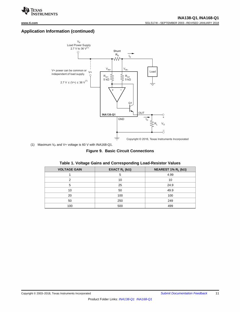
8.1.1 OperationFigure 9 illustrates the basic circuit diagram for both the INA138-Q1 and INA168-Q1. Load current IS is drawnfrom supply VP through shunt resistor RS. The voltage drop in the shunt resistor is forced across RG1 by theinternal op amp, causing current to flow into the collector of Q1. External resistor RL converts the output current,IO, to a voltage, VOUT, at the OUT pin. The transfer function for the INA1x8-Q1 is shown in Equation 3:
IO = gm (VIN+ − VIN−)
where• gm = 200 μA/V (3)
In the circuit of Figure 9, the input voltage, (VIN+ − VIN−), is equal to IS × RS. The output voltage, VOUT, is equal toIO × RL. The transconductance, gm, of the INA1x8-Q1 is 200 μA/V. The complete transfer function for the currentmeasurement amplifier in this application is shown in Equation 4:
VOUT = (IS) (RS) (200 μA/V) (RL) (4)
The maximum differential input voltage for accurate measurements is 0.5 V, producing a 100-μA output current.A differential input voltage of up to 2 V does not cause damage. Differential measurements (VIN+ and VIN− pins)must be unipolar, with a more-positive voltage applied to the VIN+ pin. If a more-negative voltage is applied to theVIN+ pin, IO goes to zero, but no damage occurs.
I
VP
Load Power Supply
Shunt
RSS
V+ power can be common or
independent of load supply.V+
VIN+ VIN–Load
RG1
5 kΩ
Q1
INA138-Q1OUT
IO+
R VL O
–
2.7 V (V+) 36 V≤ ≤(1)
2.7 V to 36 V(1)
Copyright © 2016, Texas Instruments Incorporated
RG1
5 kΩ
GND
11
INA138-Q1, INA168-Q1www.ti.com SGLS174I –SEPTEMBER 2003–REVISED JANUARY 2018
Product Folder Links: INA138-Q1 INA168-Q1
Submit Documentation FeedbackCopyright © 2003–2018, Texas Instruments Incorporated
Application Information (continued)
(1) Maximum VP and V+ voltage is 60 V with INA168-Q1.
Figure 9. Basic Circuit Connections
Table 1. Voltage Gains and Corresponding Load-Resistor ValuesVOLTAGE GAIN EXACT RL (kΩ) NEAREST 1% RL (kΩ)
1 5 4.992 10 105 25 24.910 50 49.920 100 10050 250 249100 500 499
+
RL
OPA340 ADC
R
C
IS
Buffer amplifier drives ADC without
affecting gain
INA138-Q1 or
INA168-Q1
VIN+ VIN±
RS
OUT
GND
12
INA138-Q1, INA168-Q1SGLS174I –SEPTEMBER 2003–REVISED JANUARY 2018 www.ti.com
Product Folder Links: INA138-Q1 INA168-Q1
Submit Documentation Feedback Copyright © 2003–2018, Texas Instruments Incorporated
8.2 Typical ApplicationsThe INA1x8-Q1 are designed for current-shunt measurement circuits (see Figure 9) but its basic function isuseful in a wide range of circuitry. With a little creativity, many unforeseen uses can be found in measurementand level-shifting circuits. A few ideas are illustrated in the following subsections.
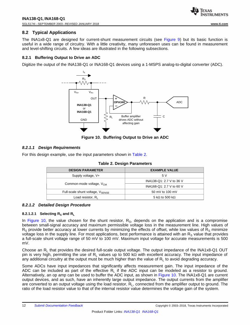
8.2.1 Buffering Output to Drive an ADCDigitize the output of the INA138-Q1 or INA168-Q1 devices using a 1-MSPS analog-to-digital converter (ADC).
Figure 10. Buffering Output to Drive an ADC
8.2.1.1 Design RequirementsFor this design example, use the input parameters shown in Table 2.
Table 2. Design ParametersDESIGN PARAMETER EXAMPLE VALUE
Supply voltage, V+ 5 V
Common-mode voltage, VCMINA138-Q1: 2.7 V to 36 VINA168-Q1: 2.7 V to 60 V
Full-scale shunt voltage, VSENSE 50 mV to 100 mVLoad resistor, RL 5 kΩ to 500 kΩ
8.2.1.2 Detailed Design Procedure
8.2.1.2.1 Selecting RS and RL
In Figure 10, the value chosen for the shunt resistor, RS, depends on the application and is a compromisebetween small-signal accuracy and maximum permissible voltage loss in the measurement line. High values ofRS provide better accuracy at lower currents by minimizing the effects of offset, while low values of RS minimizevoltage loss in the supply line. For most applications, best performance is attained with an RS value that providesa full-scale shunt voltage range of 50 mV to 100 mV. Maximum input voltage for accurate measurements is 500mV.
Choose an RL that provides the desired full-scale output voltage. The output impedance of the INA1x8-Q1 OUTpin is very high, permitting the use of RL values up to 500 kΩ with excellent accuracy. The input impedance ofany additional circuitry at the output must be much higher than the value of RL to avoid degrading accuracy.
Some ADCs have input impedances that significantly affects measurement gain. The input impedance of theADC can be included as part of the effective RL if the ADC input can be modeled as a resistor to ground.Alternatively, an op amp can be used to buffer the ADC input, as shown in Figure 10. The INA1x8-Q1 are currentoutput devices, and as such, have an inherently large output impedance. The output currents from the amplifierare converted to an output voltage using the load resistor, RL, connected from the amplifier output to ground. Theratio of the load resistor value to that of the internal resistor value determines the voltage gain of the system.
Time
Inpu
t to
AD
C (
0.25
V/d
iv)
with bufferwithout Buffer
13
INA138-Q1, INA168-Q1www.ti.com SGLS174I –SEPTEMBER 2003–REVISED JANUARY 2018
Product Folder Links: INA138-Q1 INA168-Q1
Submit Documentation FeedbackCopyright © 2003–2018, Texas Instruments Incorporated
In many applications, digitizing the output of the INA1x8-Q1 is required. Digitizing is accomplished by connectingthe output of the amplifier to an ADC. It is very common for an ADC to have a dynamic input impedance. If theINA1x8-Q1 output is connected directly to an ADC input, the input impedance of the ADC is effectively connectedin parallel with gain setting resistor RL. This parallel impedance combination affects the gain of the system andthe impact on the gain is difficult to estimate accurately. A simple solution that eliminates the paralleling ofimpedances, and simplifies the gain of the circuit is to place a buffer amplifier, such as the OPA340, between theoutput of the INA1x8-Q1 and the input to the ADC.
Figure 10 illustrates this concept. Notice that a low-pass filter is placed between the OPA340 output and theinput to the ADC. The filter capacitor is required to provide any instantaneous demand for current required by theinput stage of the ADC. The filter resistor is required to isolate the OPA340 output from the filter capacitor inorder to maintain circuit stability. The values for the filter components vary according to the operational amplifierused for the buffer and the particular ADC selected. More information regarding the design of the low-pass filteris found in the TI Precision Design, 16 bit 1MSPS Data Acquisition Reference Design for Single-EndedMultiplexed Applications.
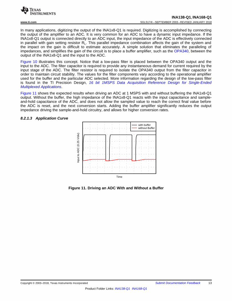
Figure 11 shows the expected results when driving an ADC at 1 MSPS with and without buffering the INA1x8-Q1output. Without the buffer, the high impedance of the INA1x8-Q1 reacts with the input capacitance and sample-and-hold capacitance of the ADC, and does not allow the sampled value to reach the correct final value beforethe ADC is reset, and the next conversion starts. Adding the buffer amplifier significantly reduces the outputimpedance driving the sample-and-hold circuitry, and allows for higher conversion rates.
8.2.1.3 Application Curve
Figure 11. Driving an ADC With and Without a Buffer
–
–
Ga
in (
dB
)
R = 500kL W
R = 50kL W
R = 5kL W
C = 10nFL C = 1nFL C = 100pFL
VO
CLR
L
2 RpLC
LINA138-Q1
f–3dB
f =–3dB
VIN+
VIN–
OUT
GND
14
INA138-Q1, INA168-Q1SGLS174I –SEPTEMBER 2003–REVISED JANUARY 2018 www.ti.com
Product Folder Links: INA138-Q1 INA168-Q1
Submit Documentation Feedback Copyright © 2003–2018, Texas Instruments Incorporated
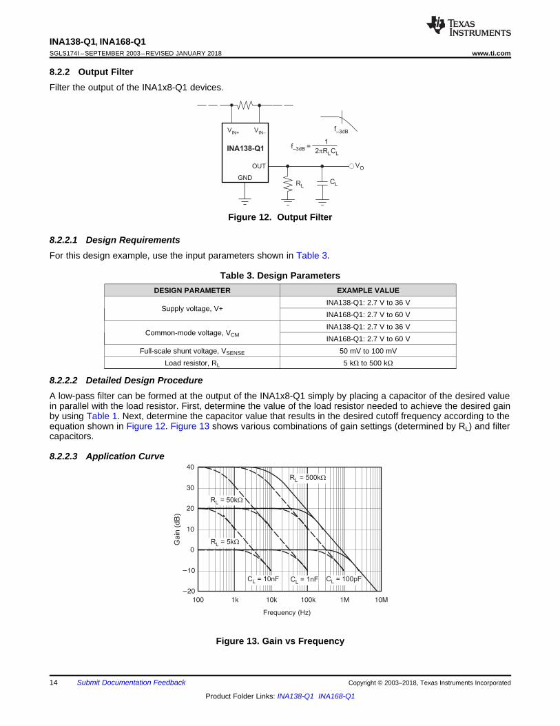
8.2.2 Output FilterFilter the output of the INA1x8-Q1 devices.
Figure 12. Output Filter
8.2.2.1 Design RequirementsFor this design example, use the input parameters shown in Table 3.
Table 3. Design ParametersDESIGN PARAMETER EXAMPLE VALUE
Supply voltage, V+INA138-Q1: 2.7 V to 36 VINA168-Q1: 2.7 V to 60 V
Common-mode voltage, VCMINA138-Q1: 2.7 V to 36 VINA168-Q1: 2.7 V to 60 V
Full-scale shunt voltage, VSENSE 50 mV to 100 mVLoad resistor, RL 5 kΩ to 500 kΩ
8.2.2.2 Detailed Design ProcedureA low-pass filter can be formed at the output of the INA1x8-Q1 simply by placing a capacitor of the desired valuein parallel with the load resistor. First, determine the value of the load resistor needed to achieve the desired gainby using Table 1. Next, determine the capacitor value that results in the desired cutoff frequency according to theequation shown in Figure 12. Figure 13 shows various combinations of gain settings (determined by RL) and filtercapacitors.
8.2.2.3 Application Curve
Figure 13. Gain vs Frequency
Output Offset =
b) Using current source.
INA138-Q1 INA138-Q1
VIN+VIN–
OUT
VIN+VIN–
OUT
Copyright © 2016, Texas Instruments Incorporated
R1
R2
VO
RL
VO
100 Aμ
Gain Set by R R||1 2
(V )RR 2
R + R1 2
a) Using resistor divider.
Gain Set by RL
Output Offset = (100 A)(R )μ L
(independent of V+)
VR
15
INA138-Q1, INA168-Q1www.ti.com SGLS174I –SEPTEMBER 2003–REVISED JANUARY 2018
Product Folder Links: INA138-Q1 INA168-Q1
Submit Documentation FeedbackCopyright © 2003–2018, Texas Instruments Incorporated
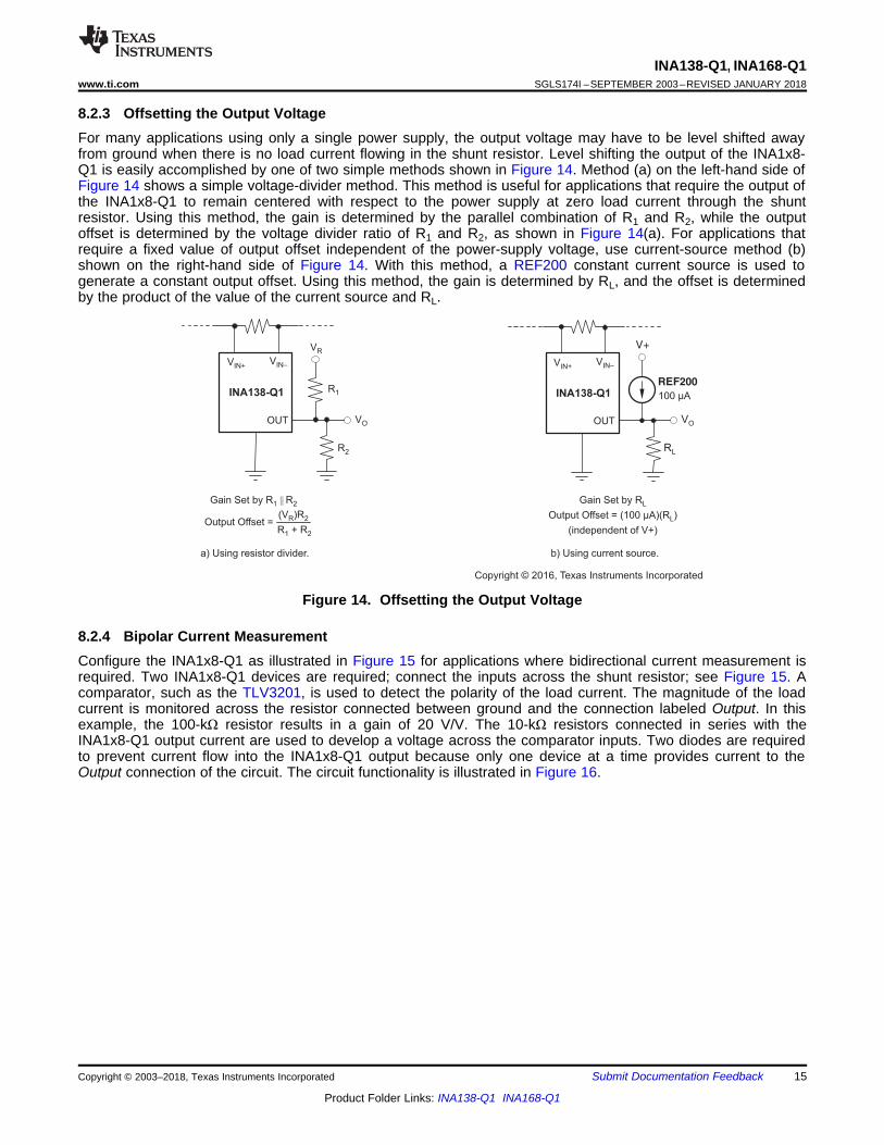
8.2.3 Offsetting the Output VoltageFor many applications using only a single power supply, the output voltage may have to be level shifted awayfrom ground when there is no load current flowing in the shunt resistor. Level shifting the output of the INA1x8-Q1 is easily accomplished by one of two simple methods shown in Figure 14. Method (a) on the left-hand side ofFigure 14 shows a simple voltage-divider method. This method is useful for applications that require the output ofthe INA1x8-Q1 to remain centered with respect to the power supply at zero load current through the shuntresistor. Using this method, the gain is determined by the parallel combination of R1 and R2, while the outputoffset is determined by the voltage divider ratio of R1 and R2, as shown in Figure 14(a). For applications thatrequire a fixed value of output offset independent of the power-supply voltage, use current-source method (b)shown on the right-hand side of Figure 14. With this method, a REF200 constant current source is used togenerate a constant output offset. Using this method, the gain is determined by RL, and the offset is determinedby the product of the value of the current source and RL.
Figure 14. Offsetting the Output Voltage
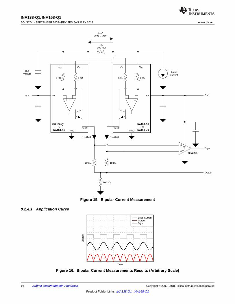
8.2.4 Bipolar Current MeasurementConfigure the INA1x8-Q1 as illustrated in Figure 15 for applications where bidirectional current measurement isrequired. Two INA1x8-Q1 devices are required; connect the inputs across the shunt resistor; see Figure 15. Acomparator, such as the TLV3201, is used to detect the polarity of the load current. The magnitude of the loadcurrent is monitored across the resistor connected between ground and the connection labeled Output. In thisexample, the 100-kΩ resistor results in a gain of 20 V/V. The 10-kΩ resistors connected in series with theINA1x8-Q1 output current are used to develop a voltage across the comparator inputs. Two diodes are requiredto prevent current flow into the INA1x8-Q1 output because only one device at a time provides current to theOutput connection of the circuit. The circuit functionality is illustrated in Figure 16.
Time
Vo
lta
ge
Load CurrentOutputSign
5 k 5 k
VIN+ VIN±
OUT
V+
GND
5 k 5 k
VIN+VIN±
OUT
V+
GND
100 m
+
INA138-Q1 or
INA168-Q1
INA138-Q1 or
INA168-Q1
1N4148 1N4148
10 k 10 k
100 k
Sign
Output
TLV3201
5 V5 V
Bus Voltage
Load Current
RS
±1-ALoad Curent
+ +
16
INA138-Q1, INA168-Q1SGLS174I –SEPTEMBER 2003–REVISED JANUARY 2018 www.ti.com
Product Folder Links: INA138-Q1 INA168-Q1
Submit Documentation Feedback Copyright © 2003–2018, Texas Instruments Incorporated
Figure 15. Bipolar Current Measurement
8.2.4.1 Application Curve
Figure 16. Bipolar Current Measurements Results (Arbitrary Scale)
INA138-Q1 INA138-Q1
ADC programmed for differential input.Depending on polarity of current, one INA138-Q1 providesan output voltage, and the output of the other device is zero.
5 V 5 V
12-BitADCMux
5 V
R
25 kΩL
RS
R
25 kΩL
VIN–
GND
VIN+ VIN–
VIN+
GND OUTOUT
17
INA138-Q1, INA168-Q1www.ti.com SGLS174I –SEPTEMBER 2003–REVISED JANUARY 2018
Product Folder Links: INA138-Q1 INA168-Q1
Submit Documentation FeedbackCopyright © 2003–2018, Texas Instruments Incorporated
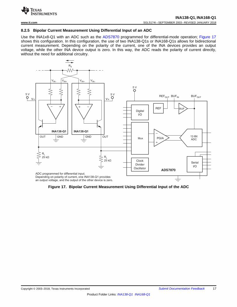
8.2.5 Bipolar Current Measurement Using Differential Input of an ADCUse the INA1x8-Q1 with an ADC such as the ADS7870 programmed for differential-mode operation; Figure 17shows this configuration. In this configuration, the use of two INA138-Q1s or INA168-Q1s allows for bidirectionalcurrent measurement. Depending on the polarity of the current, one of the INA devices provides an outputvoltage, while the other INA device output is zero. In this way, the ADC reads the polarity of current directly,without the need for additional circuitry.
Figure 17. Bipolar Current Measurement Using Differential Input of the ADC
12-BitADC
Other INA168-Q1s
INA168-Q1
INA168-Q1
Digital I/O on the ADS7870 provides power to selectthe desired INA168-Q1. Diodes prevent output current ofthe INA168-Q1 from flowing into theon off INA168-Q1.
–
–
Copyright © 2016, Texas Instruments Incorporated
Mux
5 V
18
INA138-Q1, INA168-Q1SGLS174I –SEPTEMBER 2003–REVISED JANUARY 2018 www.ti.com
Product Folder Links: INA138-Q1 INA168-Q1
Submit Documentation Feedback Copyright © 2003–2018, Texas Instruments Incorporated
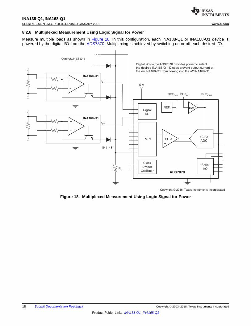
8.2.6 Multiplexed Measurement Using Logic Signal for PowerMeasure multiple loads as shown in Figure 18. In this configuration, each INA138-Q1 or INA168-Q1 device ispowered by the digital I/O from the ADS7870. Multiplexing is achieved by switching on or off each desired I/O.
Figure 18. Multiplexed Measurement Using Logic Signal for Power
NC
V+
NC
OUT
VIN-
VIN+
GND
NC
Via to Ground Plane
Via to Power Plane
RL
INA138-Q1INA168-Q1
Sense/Shunt Resistor
To Load
To Bus Voltage
Supply Bypass
Capacitor
19
INA138-Q1, INA168-Q1www.ti.com SGLS174I –SEPTEMBER 2003–REVISED JANUARY 2018
Product Folder Links: INA138-Q1 INA168-Q1
Submit Documentation FeedbackCopyright © 2003–2018, Texas Instruments Incorporated
9 Power Supply RecommendationsThe input circuitry of the INA1x8-Q1 can accurately measure beyond the power-supply voltage, V+. For example,the V+ power supply can be 5 V, whereas the load power-supply voltage goes up to 36 V with the INA138-Q1, or60 V with the INA168-Q1. However, the output voltage range of the OUT pin is limited by the lesser of the twovoltages (see the Output Voltage Range section). Place a 0.1-µF capacitor near the power-supply pin on theINA1x8-Q1. Additional capacitance may be required for applications with noisy power-supply voltages.
10 Layout
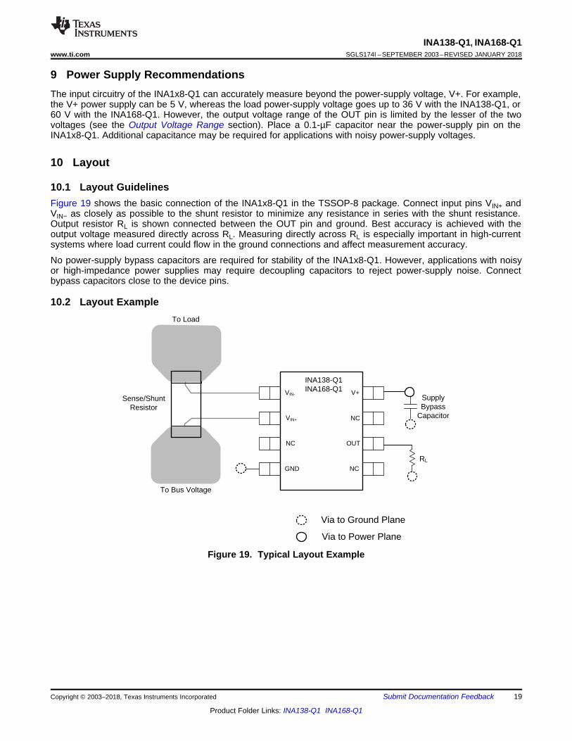
10.1 Layout GuidelinesFigure 19 shows the basic connection of the INA1x8-Q1 in the TSSOP-8 package. Connect input pins VIN+ andVIN− as closely as possible to the shunt resistor to minimize any resistance in series with the shunt resistance.Output resistor RL is shown connected between the OUT pin and ground. Best accuracy is achieved with theoutput voltage measured directly across RL. Measuring directly across RL is especially important in high-currentsystems where load current could flow in the ground connections and affect measurement accuracy.
No power-supply bypass capacitors are required for stability of the INA1x8-Q1. However, applications with noisyor high-impedance power supplies may require decoupling capacitors to reject power-supply noise. Connectbypass capacitors close to the device pins.
10.2 Layout Example
Figure 19. Typical Layout Example
20
INA138-Q1, INA168-Q1SGLS174I –SEPTEMBER 2003–REVISED JANUARY 2018 www.ti.com
Product Folder Links: INA138-Q1 INA168-Q1
Submit Documentation Feedback Copyright © 2003–2018, Texas Instruments Incorporated
11 Device And Documentation Support
11.1 Documentation Support
11.1.1 Related DocumentationFor related documentation see the following:
16 bit 1MSPS Data Acquisition Reference Design for Single-Ended Multiplexed Applications TI Precision Design
11.2 Related LinksThe table below lists quick access links. Categories include technical documents, support and communityresources, tools and software, and quick access to order now.
Table 4. Related Links
PARTS PRODUCT FOLDER ORDER NOW TECHNICALDOCUMENTS
TOOLS &SOFTWARE
SUPPORT &COMMUNITY
INA138-Q1 Click here Click here Click here Click here Click hereINA168-Q1 Click here Click here Click here Click here Click here
11.3 Community ResourcesThe following links connect to TI community resources. Linked contents are provided "AS IS" by the respectivecontributors. They do not constitute TI specifications and do not necessarily reflect TI's views; see TI's Terms ofUse.
TI E2E™ Online Community TI's Engineer-to-Engineer (E2E) Community. Created to foster collaborationamong engineers. At e2e.ti.com, you can ask questions, share knowledge, explore ideas and helpsolve problems with fellow engineers.
Design Support TI's Design Support Quickly find helpful E2E forums along with design support tools andcontact information for technical support.
11.4 TrademarksE2E is a trademark of Texas Instruments.All other trademarks are the property of their respective owners.
11.5 Electrostatic Discharge CautionThis integrated circuit can be damaged by ESD. Texas Instruments recommends that all integrated circuits be handled withappropriate precautions. Failure to observe proper handling and installation procedures can cause damage.
ESD damage can range from subtle performance degradation to complete device failure. Precision integrated circuits may be moresusceptible to damage because very small parametric changes could cause the device not to meet its published specifications.
11.6 GlossarySLYZ022 — TI Glossary.
This glossary lists and explains terms, acronyms, and definitions.
12 Mechanical, Packaging, And Orderable InformationThe following pages include mechanical, packaging, and orderable information. This information is the mostcurrent data available for the designated devices. This data is subject to change without notice and revision ofthis document. For browser-based versions of this data sheet, refer to the left-hand navigation.
PACKAGE OPTION ADDENDUM
www.ti.com 9-Mar-2017
Addendum-Page 1
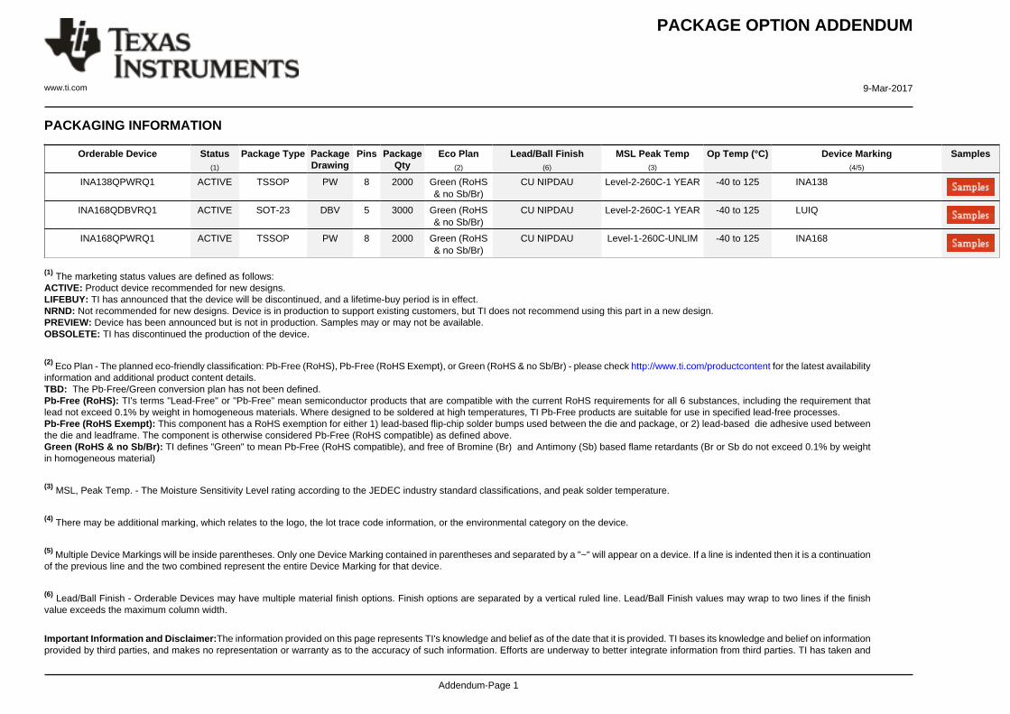
PACKAGING INFORMATION
Orderable Device Status(1)
Package Type PackageDrawing
Pins PackageQty
Eco Plan(2)
Lead/Ball Finish(6)
MSL Peak Temp(3)
Op Temp (°C) Device Marking(4/5)
Samples
INA138QPWRQ1 ACTIVE TSSOP PW 8 2000 Green (RoHS& no Sb/Br)
CU NIPDAU Level-2-260C-1 YEAR -40 to 125 INA138
INA168QDBVRQ1 ACTIVE SOT-23 DBV 5 3000 Green (RoHS& no Sb/Br)
CU NIPDAU Level-2-260C-1 YEAR -40 to 125 LUIQ
INA168QPWRQ1 ACTIVE TSSOP PW 8 2000 Green (RoHS& no Sb/Br)
CU NIPDAU Level-1-260C-UNLIM -40 to 125 INA168
(1) The marketing status values are defined as follows:ACTIVE: Product device recommended for new designs.LIFEBUY: TI has announced that the device will be discontinued, and a lifetime-buy period is in effect.NRND: Not recommended for new designs. Device is in production to support existing customers, but TI does not recommend using this part in a new design.PREVIEW: Device has been announced but is not in production. Samples may or may not be available.OBSOLETE: TI has discontinued the production of the device.
(2) Eco Plan - The planned eco-friendly classification: Pb-Free (RoHS), Pb-Free (RoHS Exempt), or Green (RoHS & no Sb/Br) - please check http://www.ti.com/productcontent for the latest availabilityinformation and additional product content details.TBD: The Pb-Free/Green conversion plan has not been defined.Pb-Free (RoHS): TI's terms "Lead-Free" or "Pb-Free" mean semiconductor products that are compatible with the current RoHS requirements for all 6 substances, including the requirement thatlead not exceed 0.1% by weight in homogeneous materials. Where designed to be soldered at high temperatures, TI Pb-Free products are suitable for use in specified lead-free processes.Pb-Free (RoHS Exempt): This component has a RoHS exemption for either 1) lead-based flip-chip solder bumps used between the die and package, or 2) lead-based die adhesive used betweenthe die and leadframe. The component is otherwise considered Pb-Free (RoHS compatible) as defined above.Green (RoHS & no Sb/Br): TI defines "Green" to mean Pb-Free (RoHS compatible), and free of Bromine (Br) and Antimony (Sb) based flame retardants (Br or Sb do not exceed 0.1% by weightin homogeneous material)
(3) MSL, Peak Temp. - The Moisture Sensitivity Level rating according to the JEDEC industry standard classifications, and peak solder temperature.
(4) There may be additional marking, which relates to the logo, the lot trace code information, or the environmental category on the device.
(5) Multiple Device Markings will be inside parentheses. Only one Device Marking contained in parentheses and separated by a "~" will appear on a device. If a line is indented then it is a continuationof the previous line and the two combined represent the entire Device Marking for that device.
(6) Lead/Ball Finish - Orderable Devices may have multiple material finish options. Finish options are separated by a vertical ruled line. Lead/Ball Finish values may wrap to two lines if the finishvalue exceeds the maximum column width.
Important Information and Disclaimer:The information provided on this page represents TI's knowledge and belief as of the date that it is provided. TI bases its knowledge and belief on informationprovided by third parties, and makes no representation or warranty as to the accuracy of such information. Efforts are underway to better integrate information from third parties. TI has taken and
PACKAGE OPTION ADDENDUM
www.ti.com 9-Mar-2017
Addendum-Page 2
continues to take reasonable steps to provide representative and accurate information but may not have conducted destructive testing or chemical analysis on incoming materials and chemicals.TI and TI suppliers consider certain information to be proprietary, and thus CAS numbers and other limited information may not be available for release.
In no event shall TI's liability arising out of such information exceed the total purchase price of the TI part(s) at issue in this document sold by TI to Customer on an annual basis.
OTHER QUALIFIED VERSIONS OF INA138-Q1, INA168-Q1 :
• Catalog: INA138, INA168
NOTE: Qualified Version Definitions:
• Catalog - TI's standard catalog product
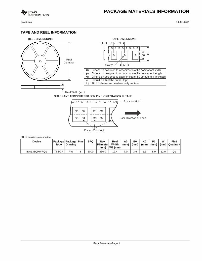
TAPE AND REEL INFORMATION
*All dimensions are nominal
Device PackageType
PackageDrawing
Pins SPQ ReelDiameter
(mm)
ReelWidth
W1 (mm)
A0(mm)
B0(mm)
K0(mm)
P1(mm)
W(mm)
Pin1Quadrant
INA138QPWRQ1 TSSOP PW 8 2000 330.0 12.4 7.0 3.6 1.6 8.0 12.0 Q1
PACKAGE MATERIALS INFORMATION
www.ti.com 13-Jan-2018
Pack Materials-Page 1
*All dimensions are nominal
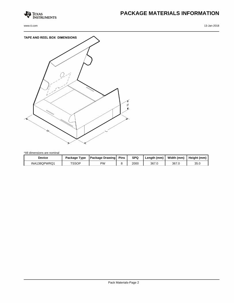
Device Package Type Package Drawing Pins SPQ Length (mm) Width (mm) Height (mm)
INA138QPWRQ1 TSSOP PW 8 2000 367.0 367.0 35.0
PACKAGE MATERIALS INFORMATION
www.ti.com 13-Jan-2018
Pack Materials-Page 2
www.ti.com
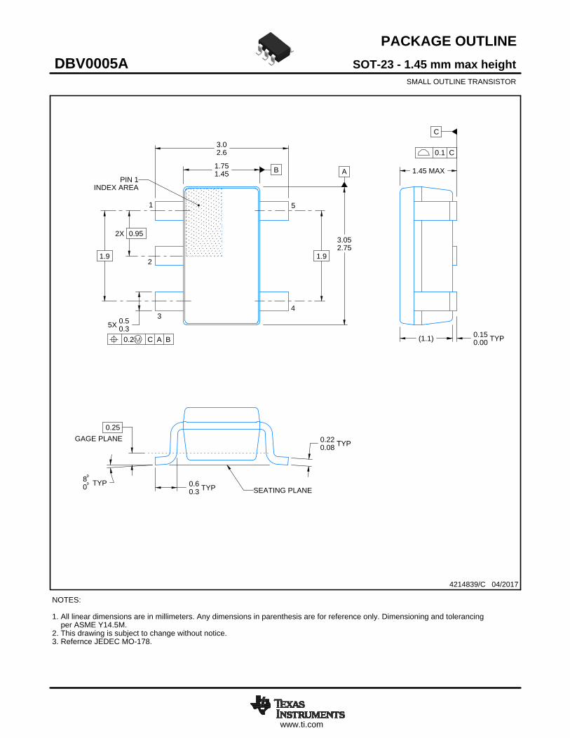
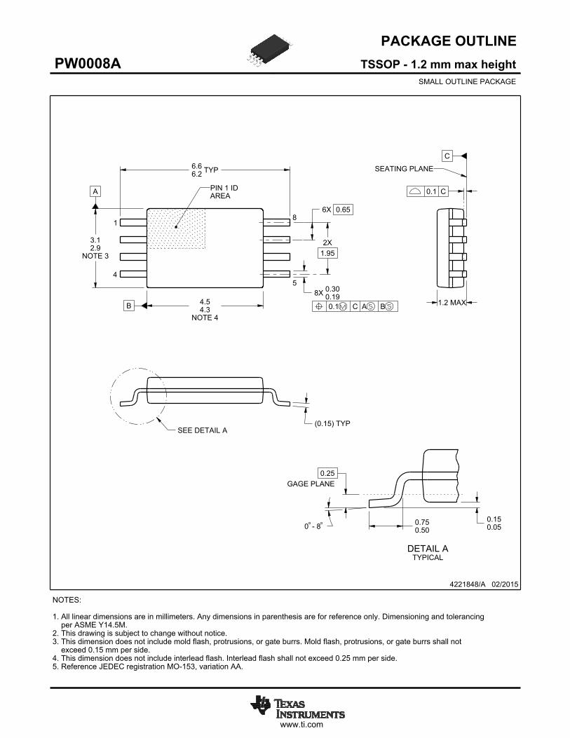
PACKAGE OUTLINE
C
TYP0.220.08
0.25
3.02.6
2X 0.95
1.9
1.45 MAX
TYP0.150.00
5X 0.50.3
TYP0.60.3
TYP80
1.9
A
3.052.75
B1.751.45
(1.1)
SOT-23 - 1.45 mm max heightDBV0005ASMALL OUTLINE TRANSISTOR
4214839/C 04/2017
NOTES: 1. All linear dimensions are in millimeters. Any dimensions in parenthesis are for reference only. Dimensioning and tolerancing per ASME Y14.5M.2. This drawing is subject to change without notice.3. Refernce JEDEC MO-178.
0.2 C A B
1
34
5
2
INDEX AREAPIN 1
GAGE PLANE
SEATING PLANE
0.1 C
SCALE 4.000
www.ti.com
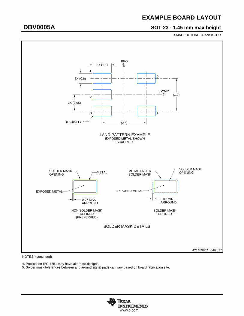
EXAMPLE BOARD LAYOUT
0.07 MAXARROUND
0.07 MINARROUND
5X (1.1)
5X (0.6)
(2.6)
(1.9)
2X (0.95)
(R0.05) TYP
4214839/C 04/2017
SOT-23 - 1.45 mm max heightDBV0005ASMALL OUTLINE TRANSISTOR
NOTES: (continued) 4. Publication IPC-7351 may have alternate designs. 5. Solder mask tolerances between and around signal pads can vary based on board fabrication site.
SYMM
LAND PATTERN EXAMPLEEXPOSED METAL SHOWN
SCALE:15X
PKG
1
3 4
5
2
SOLDER MASKOPENINGMETAL UNDER
SOLDER MASK
SOLDER MASKDEFINED
EXPOSED METAL
METALSOLDER MASKOPENING
NON SOLDER MASKDEFINED
(PREFERRED)
SOLDER MASK DETAILS
EXPOSED METAL
www.ti.com
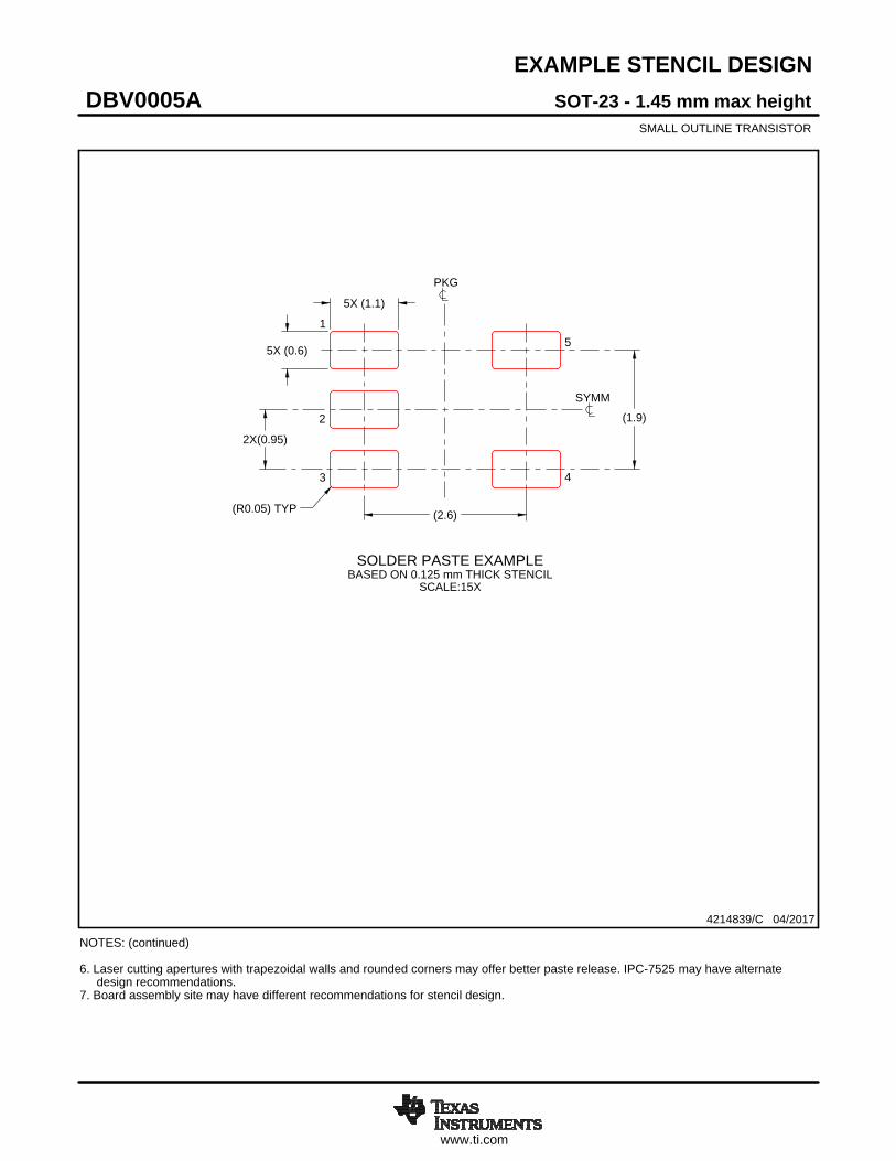
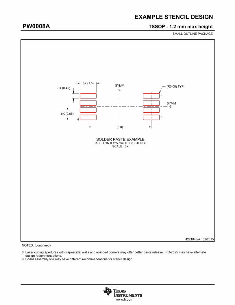
EXAMPLE STENCIL DESIGN
(2.6)
(1.9)
2X(0.95)
5X (1.1)
5X (0.6)
(R0.05) TYP
SOT-23 - 1.45 mm max heightDBV0005ASMALL OUTLINE TRANSISTOR
4214839/C 04/2017
NOTES: (continued) 6. Laser cutting apertures with trapezoidal walls and rounded corners may offer better paste release. IPC-7525 may have alternate design recommendations. 7. Board assembly site may have different recommendations for stencil design.
SOLDER PASTE EXAMPLEBASED ON 0.125 mm THICK STENCIL
SCALE:15X
SYMM
PKG
1
3 4
5
2
www.ti.com
PACKAGE OUTLINE
C
TYP6.66.2
1.2 MAX
6X 0.65
8X 0.300.19
2X1.95
0.150.05
(0.15) TYP
0 - 8
0.25GAGE PLANE
0.750.50
A
NOTE 3
3.12.9
BNOTE 4
4.54.3
4221848/A 02/2015
TSSOP - 1.2 mm max heightPW0008ASMALL OUTLINE PACKAGE
NOTES: 1. All linear dimensions are in millimeters. Any dimensions in parenthesis are for reference only. Dimensioning and tolerancing per ASME Y14.5M. 2. This drawing is subject to change without notice. 3. This dimension does not include mold flash, protrusions, or gate burrs. Mold flash, protrusions, or gate burrs shall not exceed 0.15 mm per side. 4. This dimension does not include interlead flash. Interlead flash shall not exceed 0.25 mm per side.5. Reference JEDEC registration MO-153, variation AA.
18
0.1 C A B
54
PIN 1 IDAREA
SEATING PLANE
0.1 C
SEE DETAIL A
DETAIL ATYPICAL
SCALE 2.800
www.ti.com
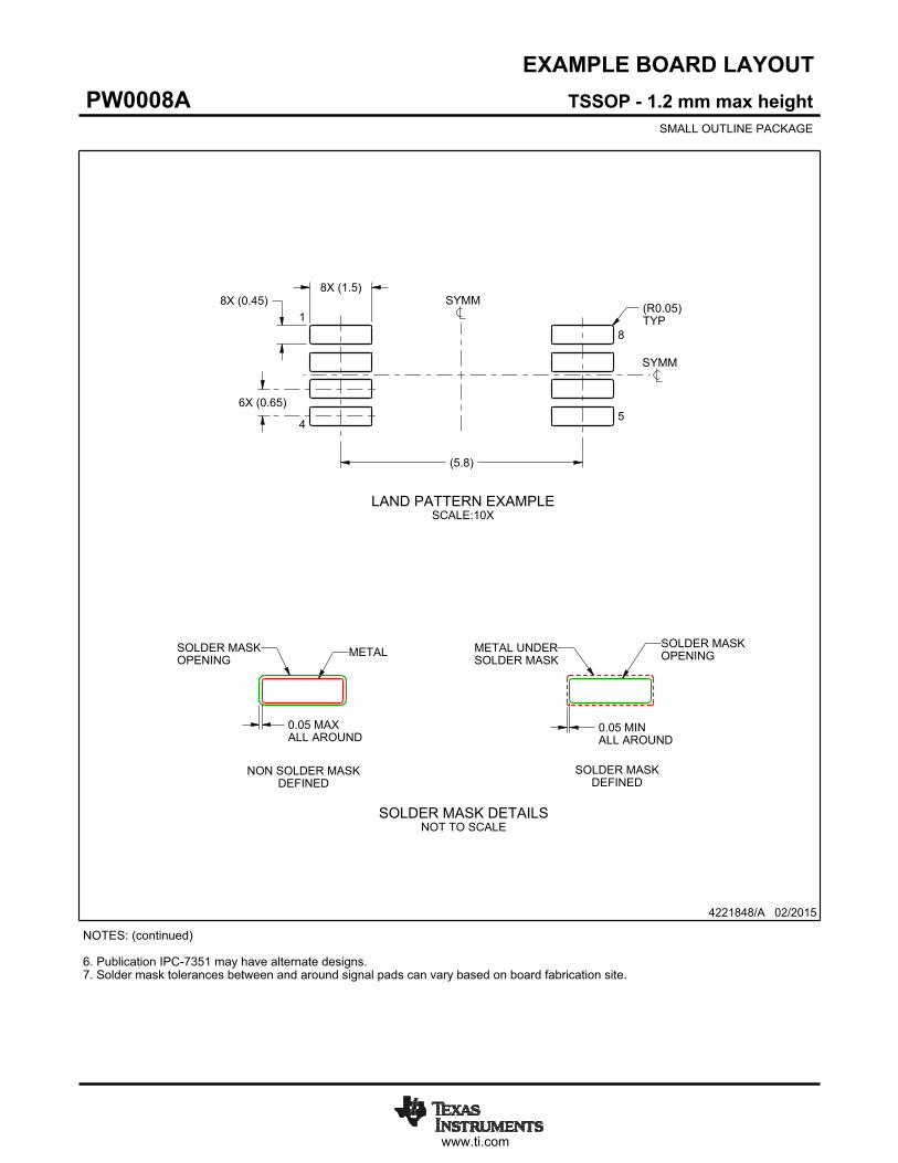
EXAMPLE BOARD LAYOUT
(5.8)
0.05 MAXALL AROUND
0.05 MINALL AROUND
8X (1.5)8X (0.45)
6X (0.65)
(R )TYP
0.05
4221848/A 02/2015
TSSOP - 1.2 mm max heightPW0008ASMALL OUTLINE PACKAGE
SYMM
SYMM
LAND PATTERN EXAMPLESCALE:10X
1
45
8
NOTES: (continued) 6. Publication IPC-7351 may have alternate designs. 7. Solder mask tolerances between and around signal pads can vary based on board fabrication site.
METALSOLDER MASKOPENING
NON SOLDER MASKDEFINED
SOLDER MASK DETAILSNOT TO SCALE
SOLDER MASKOPENING
METAL UNDERSOLDER MASK
SOLDER MASKDEFINED
www.ti.com
EXAMPLE STENCIL DESIGN
(5.8)
6X (0.65)
8X (0.45)8X (1.5)
(R ) TYP0.05
4221848/A 02/2015
TSSOP - 1.2 mm max heightPW0008ASMALL OUTLINE PACKAGE
NOTES: (continued) 8. Laser cutting apertures with trapezoidal walls and rounded corners may offer better paste release. IPC-7525 may have alternate design recommendations. 9. Board assembly site may have different recommendations for stencil design.
SYMM
SYMM
1
45
8
SOLDER PASTE EXAMPLEBASED ON 0.125 mm THICK STENCIL
SCALE:10X
IMPORTANT NOTICE
Texas Instruments Incorporated (TI) reserves the right to make corrections, enhancements, improvements and other changes to itssemiconductor products and services per JESD46, latest issue, and to discontinue any product or service per JESD48, latest issue. Buyersshould obtain the latest relevant information before placing orders and should verify that such information is current and complete.TI’s published terms of sale for semiconductor products (http://www.ti.com/sc/docs/stdterms.htm) apply to the sale of packaged integratedcircuit products that TI has qualified and released to market. Additional terms may apply to the use or sale of other types of TI products andservices.Reproduction of significant portions of TI information in TI data sheets is permissible only if reproduction is without alteration and isaccompanied by all associated warranties, conditions, limitations, and notices. TI is not responsible or liable for such reproduceddocumentation. Information of third parties may be subject to additional restrictions. Resale of TI products or services with statementsdifferent from or beyond the parameters stated by TI for that product or service voids all express and any implied warranties for theassociated TI product or service and is an unfair and deceptive business practice. TI is not responsible or liable for any such statements.Buyers and others who are developing systems that incorporate TI products (collectively, “Designers”) understand and agree that Designersremain responsible for using their independent analysis, evaluation and judgment in designing their applications and that Designers havefull and exclusive responsibility to assure the safety of Designers' applications and compliance of their applications (and of all TI productsused in or for Designers’ applications) with all applicable regulations, laws and other applicable requirements. Designer represents that, withrespect to their applications, Designer has all the necessary expertise to create and implement safeguards that (1) anticipate dangerousconsequences of failures, (2) monitor failures and their consequences, and (3) lessen the likelihood of failures that might cause harm andtake appropriate actions. Designer agrees that prior to using or distributing any applications that include TI products, Designer willthoroughly test such applications and the functionality of such TI products as used in such applications.TI’s provision of technical, application or other design advice, quality characterization, reliability data or other services or information,including, but not limited to, reference designs and materials relating to evaluation modules, (collectively, “TI Resources”) are intended toassist designers who are developing applications that incorporate TI products; by downloading, accessing or using TI Resources in anyway, Designer (individually or, if Designer is acting on behalf of a company, Designer’s company) agrees to use any particular TI Resourcesolely for this purpose and subject to the terms of this Notice.TI’s provision of TI Resources does not expand or otherwise alter TI’s applicable published warranties or warranty disclaimers for TIproducts, and no additional obligations or liabilities arise from TI providing such TI Resources. TI reserves the right to make corrections,enhancements, improvements and other changes to its TI Resources. TI has not conducted any testing other than that specificallydescribed in the published documentation for a particular TI Resource.Designer is authorized to use, copy and modify any individual TI Resource only in connection with the development of applications thatinclude the TI product(s) identified in such TI Resource. NO OTHER LICENSE, EXPRESS OR IMPLIED, BY ESTOPPEL OR OTHERWISETO ANY OTHER TI INTELLECTUAL PROPERTY RIGHT, AND NO LICENSE TO ANY TECHNOLOGY OR INTELLECTUAL PROPERTYRIGHT OF TI OR ANY THIRD PARTY IS GRANTED HEREIN, including but not limited to any patent right, copyright, mask work right, orother intellectual property right relating to any combination, machine, or process in which TI products or services are used. Informationregarding or referencing third-party products or services does not constitute a license to use such products or services, or a warranty orendorsement thereof. Use of TI Resources may require a license from a third party under the patents or other intellectual property of thethird party, or a license from TI under the patents or other intellectual property of TI.TI RESOURCES ARE PROVIDED “AS IS” AND WITH ALL FAULTS. TI DISCLAIMS ALL OTHER WARRANTIES ORREPRESENTATIONS, EXPRESS OR IMPLIED, REGARDING RESOURCES OR USE THEREOF, INCLUDING BUT NOT LIMITED TOACCURACY OR COMPLETENESS, TITLE, ANY EPIDEMIC FAILURE WARRANTY AND ANY IMPLIED WARRANTIES OFMERCHANTABILITY, FITNESS FOR A PARTICULAR PURPOSE, AND NON-INFRINGEMENT OF ANY THIRD PARTY INTELLECTUALPROPERTY RIGHTS. TI SHALL NOT BE LIABLE FOR AND SHALL NOT DEFEND OR INDEMNIFY DESIGNER AGAINST ANY CLAIM,INCLUDING BUT NOT LIMITED TO ANY INFRINGEMENT CLAIM THAT RELATES TO OR IS BASED ON ANY COMBINATION OFPRODUCTS EVEN IF DESCRIBED IN TI RESOURCES OR OTHERWISE. IN NO EVENT SHALL TI BE LIABLE FOR ANY ACTUAL,DIRECT, SPECIAL, COLLATERAL, INDIRECT, PUNITIVE, INCIDENTAL, CONSEQUENTIAL OR EXEMPLARY DAMAGES INCONNECTION WITH OR ARISING OUT OF TI RESOURCES OR USE THEREOF, AND REGARDLESS OF WHETHER TI HAS BEENADVISED OF THE POSSIBILITY OF SUCH DAMAGES.Unless TI has explicitly designated an individual product as meeting the requirements of a particular industry standard (e.g., ISO/TS 16949and ISO 26262), TI is not responsible for any failure to meet such industry standard requirements.Where TI specifically promotes products as facilitating functional safety or as compliant with industry functional safety standards, suchproducts are intended to help enable customers to design and create their own applications that meet applicable functional safety standardsand requirements. Using products in an application does not by itself establish any safety features in the application. Designers mustensure compliance with safety-related requirements and standards applicable to their applications. Designer may not use any TI products inlife-critical medical equipment unless authorized officers of the parties have executed a special contract specifically governing such use.Life-critical medical equipment is medical equipment where failure of such equipment would cause serious bodily injury or death (e.g., lifesupport, pacemakers, defibrillators, heart pumps, neurostimulators, and implantables). Such equipment includes, without limitation, allmedical devices identified by the U.S. Food and Drug Administration as Class III devices and equivalent classifications outside the U.S.TI may expressly designate certain products as completing a particular qualification (e.g., Q100, Military Grade, or Enhanced Product).Designers agree that it has the necessary expertise to select the product with the appropriate qualification designation for their applicationsand that proper product selection is at Designers’ own risk. Designers are solely responsible for compliance with all legal and regulatoryrequirements in connection with such selection.Designer will fully indemnify TI and its representatives against any damages, costs, losses, and/or liabilities arising out of Designer’s non-compliance with the terms and provisions of this Notice.
Mailing Address: Texas Instruments, Post Office Box 655303, Dallas, Texas 75265Copyright © 2018, Texas Instruments Incorporated