Embed Size (px)
Citation preview
´ Power Register
Current RegisterI C-/SMBUS-Compatible
Interface
2
Voltage Register
VIN+ VIN-
VS
(Supply Voltage)
A0
A1
Data
CLK
ADCPGA
INA219
GND
Product
Folder
Sample &Buy
Technical
Documents
Tools &
Software
Support &Community
INA219SBOS448G –AUGUST 2008–REVISED DECEMBER 2015
INA219 Zerø-Drift, Bidirectional Current/Power Monitor With I2C Interface1 Features 3 Description
The INA219 is a current shunt and power monitor1• Senses Bus Voltages from 0 to 26 V
with an I2C- or SMBUS-compatible interface. The• Reports Current, Voltage, and Power device monitors both shunt voltage drop and bus• 16 Programmable Addresses supply voltage, with programmable conversion times
and filtering. A programmable calibration value,• High Accuracy: 0.5% (Maximum) Overcombined with an internal multiplier, enables directTemperature (INA219B)readouts of current in amperes. An additional• Filtering Options multiplying register calculates power in watts. The
• Calibration Registers I2C- or SMBUS-compatible interface features 16programmable addresses.• SOT23-8 and SOIC-8 PackagesThe INA219 is available in two grades: A and B. The2 Applications B grade version has higher accuracy and higherprecision specifications.• Servers
• Telecom Equipment The INA219 senses across shunts on buses that canvary from 0 to 26 V. The device uses a single 3- to• Notebook Computers5.5-V supply, drawing a maximum of 1 mA of supply• Power Management current. The INA219 operates from –40°C to 125°C.
• Battery ChargersDevice Information(1)• Welding Equipment
PART NUMBER PACKAGE BODY SIZE (NOM)• Power SuppliesSOIC (8) 3.91 mm × 4.90 mm• Test Equipment INA219SOT-23 (8) 1.63 mm × 2.90 mm
(1) For all available packages, see the orderable addendum atthe end of the data sheet.
Simplified Schematic
1
An IMPORTANT NOTICE at the end of this data sheet addresses availability, warranty, changes, use in safety-critical applications,intellectual property matters and other important disclaimers. PRODUCTION DATA.
INA219SBOS448G –AUGUST 2008–REVISED DECEMBER 2015 www.ti.com
Table of Contents8.3 Feature Description................................................... 91 Features .................................................................. 18.4 Device Functional Modes........................................ 112 Applications ........................................................... 18.5 Programming........................................................... 123 Description ............................................................. 18.6 Register Maps ........................................................ 184 Revision History..................................................... 2
9 Application and Implementation ........................ 255 Related Products ................................................... 39.1 Application Information............................................ 256 Pin Configuration and Functions ......................... 39.2 Typical Application ................................................. 257 Specifications......................................................... 4 10 Power Supply Recommendations ..................... 277.1 Absolute Maximum Ratings ...................................... 4
11 Layout................................................................... 277.2 ESD Ratings.............................................................. 411.1 Layout Guidelines ................................................. 277.3 Recommended Operating Conditions....................... 411.2 Layout Example .................................................... 277.4 Thermal Information .................................................. 4
12 Device and Documentation Support ................. 287.5 Electrical Characteristics:.......................................... 512.1 Community Resources.......................................... 287.6 Bus Timing Diagram Definitions................................ 612.2 Trademarks ........................................................... 287.7 Typical Characteristics .............................................. 712.3 Electrostatic Discharge Caution............................ 288 Detailed Description .............................................. 912.4 Glossary ................................................................ 288.1 Overview ................................................................... 9
13 Mechanical, Packaging, and Orderable8.2 Functional Block Diagram ......................................... 9Information ........................................................... 28
4 Revision HistoryNOTE: Page numbers for previous revisions may differ from page numbers in the current version.
Changes from Revision F (September 2011) to Revision G Page
• Added ESD Ratings table, Feature Description section, Device Functional Modes, Application and Implementationsection, Power Supply Recommendations section, Layout section, Device and Documentation Support section, andMechanical, Packaging, and Orderable Information section ................................................................................................. 1
• Updated Bus Timing Diagram Definitions table. I2C timing table values were previously based on simulation and notcharacterized .......................................................................................................................................................................... 6
Changes from Revision E (September 2010) to Revision F Page
• Changed step 5 and step 6 values in Table 8...................................................................................................................... 26
Changes from Revision D (September 2010) to Revision E Page
• Updated Packaging Information table .................................................................................................................................... 3
2 Submit Documentation Feedback Copyright © 2008–2015, Texas Instruments Incorporated
Product Folder Links: INA219
1
2
3
4
8
7
6
5
IN+
IN–
GND
VS
A1
A0
SDA
SCL
1
2
3
4
8
7
6
5
A1
A0
SDA
SCL
IN+
IN–
GND
VS
INA219www.ti.com SBOS448G –AUGUST 2008–REVISED DECEMBER 2015
5 Related Products
DEVICE DESCRIPTION
INA209 Current/power monitor with watchdog, peak-hold, and fast comparator functions
INA210, INA211, INA212, INA213, INA214 Zerø-drift, low-cost, analog current shunt monitor series in small package
6 Pin Configuration and Functions
DCN PackageD Package8-Pin SOT-238-Pin SOICTop ViewTop View
Pin FunctionsPIN
I/O DESCRIPTIONNAME SOT-23 SOIC
AnalogIN+ 1 8 Positive differential shunt voltage. Connect to positive side of shunt resistor.InputAnalog Negative differential shunt voltage. Connect to negative side of shunt resistor. Bus voltage isIN– 2 7 Input measured from this pin to ground.
GND 3 6 Analog GroundVS 4 5 Analog Power supply, 3 to 5.5 V
DigitalSCL 5 4 Serial bus clock lineInputDigitalSDA 6 3 Serial bus data lineI/ODigitalA0 7 2 Address pin. Table 1 shows pin settings and corresponding addresses.InputDigitalA1 8 1 Address pin. Table 1 shows pin settings and corresponding addresses.Input
Copyright © 2008–2015, Texas Instruments Incorporated Submit Documentation Feedback 3
Product Folder Links: INA219
INA219SBOS448G –AUGUST 2008–REVISED DECEMBER 2015 www.ti.com
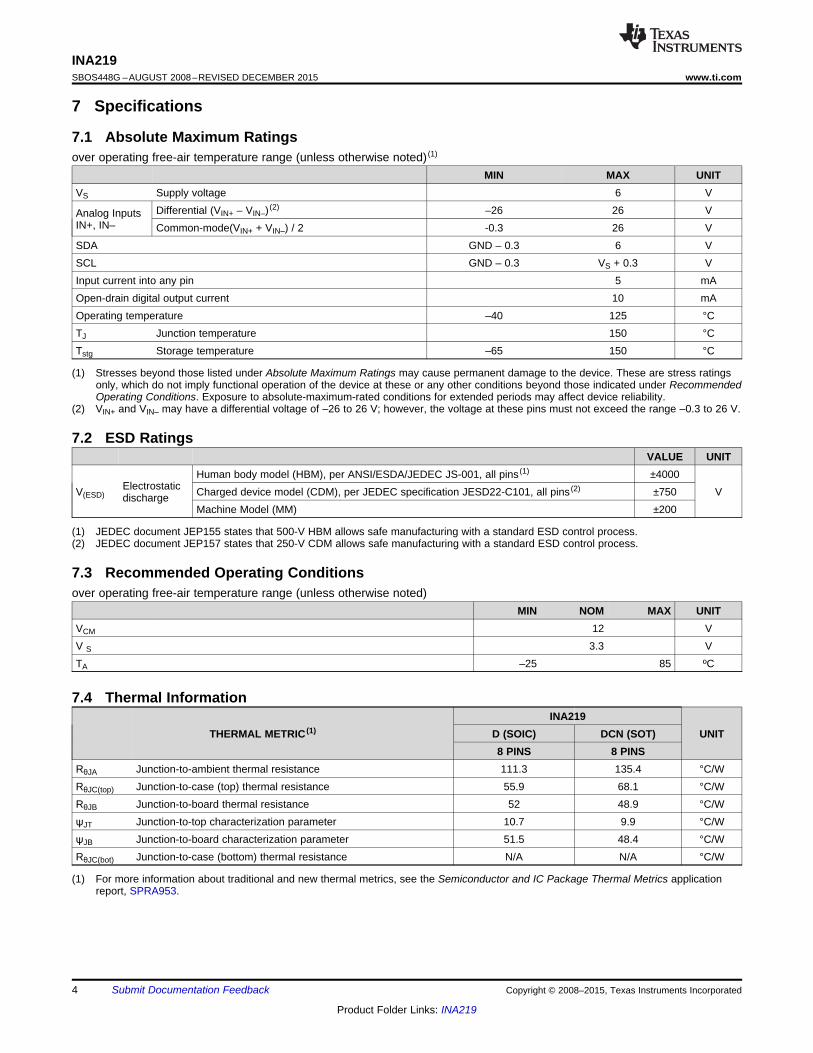
7 Specifications
7.1 Absolute Maximum Ratingsover operating free-air temperature range (unless otherwise noted) (1)
MIN MAX UNITVS Supply voltage 6 V
Differential (VIN+ – VIN–) (2) –26 26 VAnalog InputsIN+, IN– Common-mode(VIN+ + VIN–) / 2 -0.3 26 VSDA GND – 0.3 6 VSCL GND – 0.3 VS + 0.3 VInput current into any pin 5 mAOpen-drain digital output current 10 mAOperating temperature –40 125 °CTJ Junction temperature 150 °CTstg Storage temperature –65 150 °C
(1) Stresses beyond those listed under Absolute Maximum Ratings may cause permanent damage to the device. These are stress ratingsonly, which do not imply functional operation of the device at these or any other conditions beyond those indicated under RecommendedOperating Conditions. Exposure to absolute-maximum-rated conditions for extended periods may affect device reliability.
(2) VIN+ and VIN– may have a differential voltage of –26 to 26 V; however, the voltage at these pins must not exceed the range –0.3 to 26 V.
7.2 ESD RatingsVALUE UNIT
Human body model (HBM), per ANSI/ESDA/JEDEC JS-001, all pins (1) ±4000ElectrostaticV(ESD) Charged device model (CDM), per JEDEC specification JESD22-C101, all pins (2) ±750 Vdischarge
Machine Model (MM) ±200
(1) JEDEC document JEP155 states that 500-V HBM allows safe manufacturing with a standard ESD control process.(2) JEDEC document JEP157 states that 250-V CDM allows safe manufacturing with a standard ESD control process.
7.3 Recommended Operating Conditionsover operating free-air temperature range (unless otherwise noted)
MIN NOM MAX UNITVCM 12 VV S 3.3 VTA –25 85 ºC
7.4 Thermal InformationINA219
THERMAL METRIC (1) D (SOIC) DCN (SOT) UNIT8 PINS 8 PINS
RθJA Junction-to-ambient thermal resistance 111.3 135.4 °C/WRθJC(top) Junction-to-case (top) thermal resistance 55.9 68.1 °C/WRθJB Junction-to-board thermal resistance 52 48.9 °C/WψJT Junction-to-top characterization parameter 10.7 9.9 °C/WψJB Junction-to-board characterization parameter 51.5 48.4 °C/WRθJC(bot) Junction-to-case (bottom) thermal resistance N/A N/A °C/W
(1) For more information about traditional and new thermal metrics, see the Semiconductor and IC Package Thermal Metrics applicationreport, SPRA953.
4 Submit Documentation Feedback Copyright © 2008–2015, Texas Instruments Incorporated
Product Folder Links: INA219
INA219www.ti.com SBOS448G –AUGUST 2008–REVISED DECEMBER 2015
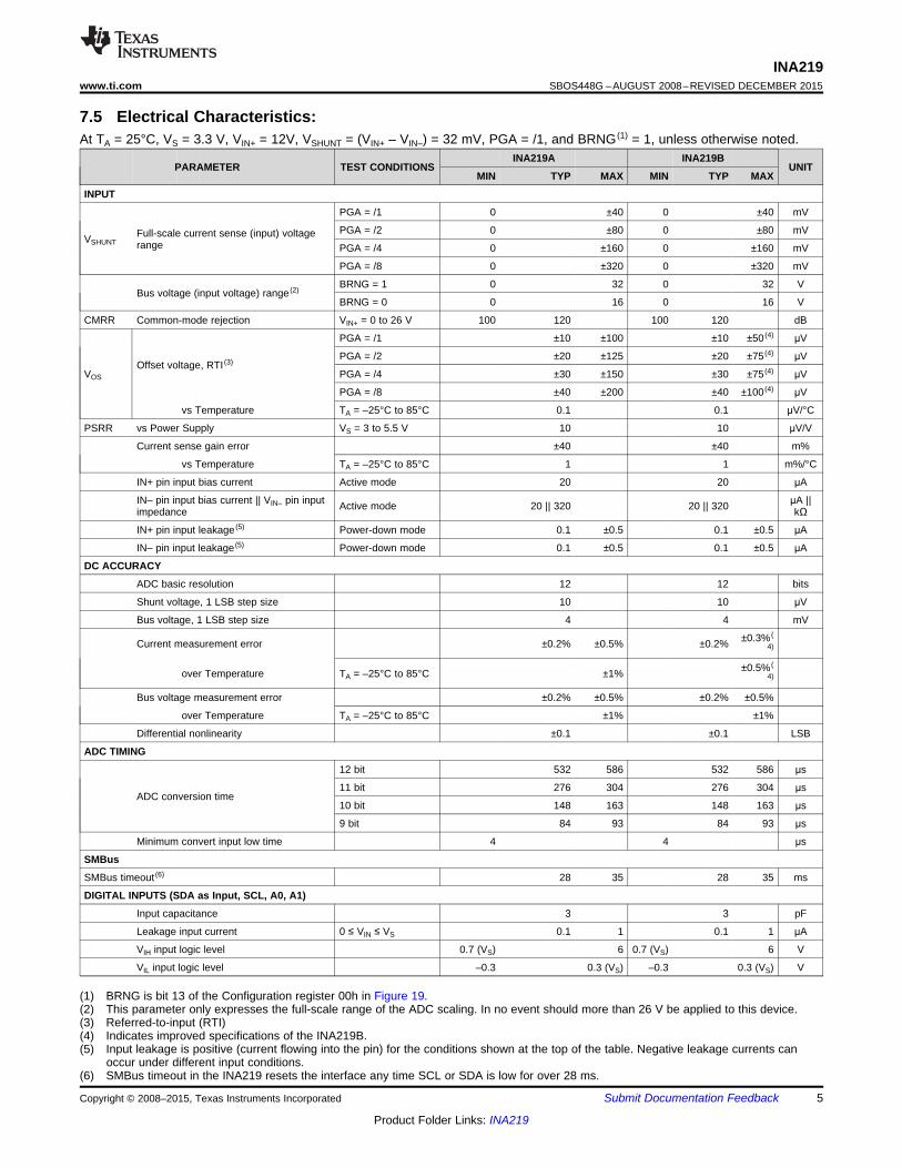
7.5 Electrical Characteristics:At TA = 25°C, VS = 3.3 V, VIN+ = 12V, VSHUNT = (VIN+ – VIN–) = 32 mV, PGA = /1, and BRNG (1) = 1, unless otherwise noted.
INA219A INA219BPARAMETER TEST CONDITIONS UNIT
MIN TYP MAX MIN TYP MAX
INPUT
PGA = /1 0 ±40 0 ±40 mV
PGA = /2 0 ±80 0 ±80 mVFull-scale current sense (input) voltageVSHUNT range PGA = /4 0 ±160 0 ±160 mV
PGA = /8 0 ±320 0 ±320 mV
BRNG = 1 0 32 0 32 VBus voltage (input voltage) range (2)
BRNG = 0 0 16 0 16 V
CMRR Common-mode rejection VIN+ = 0 to 26 V 100 120 100 120 dB
PGA = /1 ±10 ±100 ±10 ±50 (4) μV
PGA = /2 ±20 ±125 ±20 ±75 (4) μVOffset voltage, RTI (3)
VOS PGA = /4 ±30 ±150 ±30 ±75 (4) μV
PGA = /8 ±40 ±200 ±40 ±100 (4) μV
vs Temperature TA = –25°C to 85°C 0.1 0.1 μV/°C
PSRR vs Power Supply VS = 3 to 5.5 V 10 10 μV/V
Current sense gain error ±40 ±40 m%
vs Temperature TA = –25°C to 85°C 1 1 m%/°C
IN+ pin input bias current Active mode 20 20 μA
IN– pin input bias current || VIN– pin input μA ||Active mode 20 || 320 20 || 320impedance kΩ
IN+ pin input leakage (5) Power-down mode 0.1 ±0.5 0.1 ±0.5 μA
IN– pin input leakage (5) Power-down mode 0.1 ±0.5 0.1 ±0.5 μA
DC ACCURACY
ADC basic resolution 12 12 bits
Shunt voltage, 1 LSB step size 10 10 μV
Bus voltage, 1 LSB step size 4 4 mV
±0.3% (Current measurement error ±0.2% ±0.5% ±0.2% 4)
±0.5% (over Temperature TA = –25°C to 85°C ±1% 4)
Bus voltage measurement error ±0.2% ±0.5% ±0.2% ±0.5%
over Temperature TA = –25°C to 85°C ±1% ±1%
Differential nonlinearity ±0.1 ±0.1 LSB
ADC TIMING
12 bit 532 586 532 586 μs
11 bit 276 304 276 304 μsADC conversion time
10 bit 148 163 148 163 μs
9 bit 84 93 84 93 μs
Minimum convert input low time 4 4 μs
SMBus
SMBus timeout (6) 28 35 28 35 ms
DIGITAL INPUTS (SDA as Input, SCL, A0, A1)
Input capacitance 3 3 pF
Leakage input current 0 ≤ VIN ≤ VS 0.1 1 0.1 1 μA
VIH input logic level 0.7 (VS) 6 0.7 (VS) 6 V
VIL input logic level –0.3 0.3 (VS) –0.3 0.3 (VS) V
(1) BRNG is bit 13 of the Configuration register 00h in Figure 19.(2) This parameter only expresses the full-scale range of the ADC scaling. In no event should more than 26 V be applied to this device.(3) Referred-to-input (RTI)(4) Indicates improved specifications of the INA219B.(5) Input leakage is positive (current flowing into the pin) for the conditions shown at the top of the table. Negative leakage currents can
occur under different input conditions.(6) SMBus timeout in the INA219 resets the interface any time SCL or SDA is low for over 28 ms.
Copyright © 2008–2015, Texas Instruments Incorporated Submit Documentation Feedback 5
Product Folder Links: INA219
SCL
SDA
t(LOW)tR tF t(HDSTA)
t(HDSTA)
t(HDDAT)
t(BUF)
t(SUDAT)
t(HIGH) t(SUSTA)t(SUSTO)
P S S P
INA219SBOS448G –AUGUST 2008–REVISED DECEMBER 2015 www.ti.com
Electrical Characteristics: (continued)At TA = 25°C, VS = 3.3 V, VIN+ = 12V, VSHUNT = (VIN+ – VIN–) = 32 mV, PGA = /1, and BRNG(1) = 1, unless otherwise noted.
INA219A INA219BPARAMETER TEST CONDITIONS UNIT
MIN TYP MAX MIN TYP MAX
Hysteresis 500 500 mV
OPEN-DRAIN DIGITAL OUTPUTS (SDA)
Logic 0 output level ISINK = 3 mA 0.15 0.4 0.15 0.4 V
High-level output leakage current VOUT = VS 0.1 1 0.1 1 μA
POWER SUPPLY
Operating supply range 3 5.5 3 5.5 V
Quiescent current 0.7 1 0.7 1 mA
Quiescent current, power-down mode 6 15 6 15 μA
Power-on reset threshold 2 2 V
7.6 Bus Timing Diagram Definitions (1)
FAST MODE HIGH-SPEED MODEUNIT
MIN MAX MIN MAXƒ(SCL) SCL operating frequency 0.001 0.4 0.001 2.56 MHz
Bus free time between STOP and STARTt(BUF) 1300 160 nsconditionHold time after repeated START condition.t(HDSTA) 600 160 nsAfter this period, the first clock is generated.
t(SUSTA) Repeated START condition setup time 600 160 nst(SUSTO) STOP condition setup time 600 160 nst(HDDAT) Data hold time 0 900 0 90 nst(SUDAT) Data setup time 100 10 nst(LOW) SCL clock LOW period 1300 250 nst(HIGH) SCL clock HIGH period 600 60 nstF DA Data fall time 300 150 nstFCL Clock fall time 300 40 nstRCL Clock rise time 300 40 nstRCL Clock rise time for SCLK ≤ 100kHz 1000 ns
(1) Values based on a statistical analysis of a one-time sample of devices. Minimum and maximum values are not ensured and notproduction tested.
Figure 1. Bus Timing Diagram
6 Submit Documentation Feedback Copyright © 2008–2015, Texas Instruments Incorporated
Product Folder Links: INA219
-40 -25 0 25 50 75 100 125
100
80
60
40
20
0
-20
-40
-60
-80
-100
Gain
Err
or
(m%
)
Temperature ( C)°
32V
16V
20
15
10
5
0
-5
-10
-15
-20
-0.4 -0.3 -0.2 -0.1 0 0.1 0.2 0.3
INL
(V
)m
Input Voltage (V)
0.4
100
80
60
40
20
0
-20
-40
-60
-80
-100-40 -25 0 25 50 75 100
Gain
Err
or
(m%
)
Temperature ( C)°
125
320mV Range 160mV Range
80mV Range 40mV Range
50
45
40
35
30
25
20
15
10
5
0-40 -25 0 25 50 75 100
Offset (m
V)
Temperature ( C)°
125
32V Range 16V Range
0
-10
-20
-30
-40
-50
-60
-70
-80
-90
-10010 100 1k 10k 100k 1M
Gain
(dB
)
Input Frequency (Hz)
100
80
60
40
20
0
-20
-40
-60
-80
-100-40 -25 0 25 50 75 100
Offset (
V)
m
Temperature ( C)°
125
160mV Range
320mV Range
80mV Range 40mV Range
INA219www.ti.com SBOS448G –AUGUST 2008–REVISED DECEMBER 2015
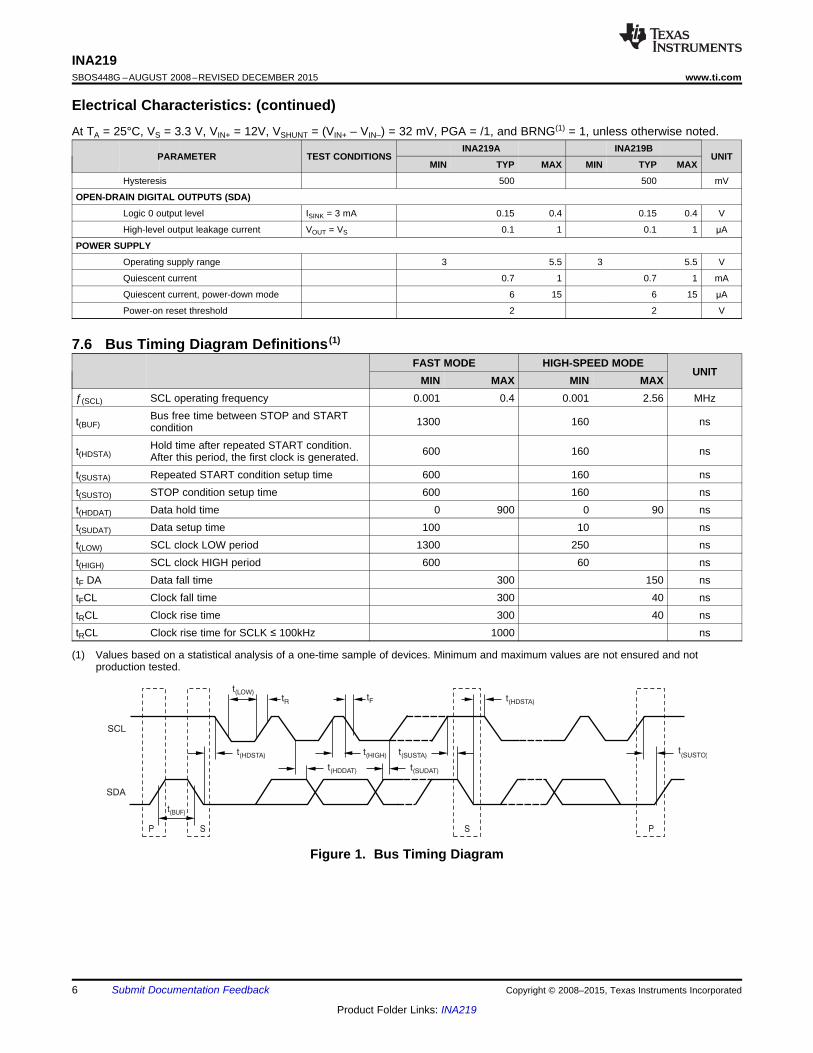
7.7 Typical CharacteristicsAt TA = 25°C, VS = 3.3 V, VIN+ = 12 V, VSHUNT = (VIN+ – VIN–) = 32 mV, PGA = /1, and BRNG = 1, unless otherwise noted.
Figure 2. Frequency Response Figure 3. ADC Shunt Offset vs Temperature
Figure 4. ADC Shunt Gain Error vs Temperature Figure 5. ADC Bus Voltage Offset vs Temperature
Figure 7. Integral Nonlinearity vs Input VoltageFigure 6. ADC Bus Gain Error vs Temperature
Copyright © 2008–2015, Texas Instruments Incorporated Submit Documentation Feedback 7
Product Folder Links: INA219
300
250
200
150
100
50
0
1k 10k 100k 1M 10M
I(
A)
Qm
SCL Frequency (Hz)
V = 5VS
V = 3VS
1.0
0.9
0.8
0.7
0.6
0.5
0.4
0.3
0.2
0.1
0
1k 10k 100k 1M 10M
I Q(m
A)
SCL Frequency (Hz)
V = 5VS
V =S 3V
16
14
12
10
8
6
4
2
0
-40 -25 0 25 125
I(
A)
mQ
Temperature ( C)°
V = 5VS
V = 3VS
50 75 100
1.2
1.0
0.8
0.6
0.4
0.2
0
-40 -25 0 25 50 75 100
I(m
A)
Q
Temperature ( C)°
125
V = 3VS
V = 5VS
2.0
1.5
1.0
0.5
0
-0.5
-1.0
-1.5
0 5 10 15 20 25
Inp
ut
Cu
rre
nts
(m
A)
V Voltage (V)IN-
30
VS+ = 5V
V 5VS+ =
VS+ = 3V
V 3VS+ =
INA219SBOS448G –AUGUST 2008–REVISED DECEMBER 2015 www.ti.com
Typical Characteristics (continued)At TA = 25°C, VS = 3.3 V, VIN+ = 12 V, VSHUNT = (VIN+ – VIN–) = 32 mV, PGA = /1, and BRNG = 1, unless otherwise noted.
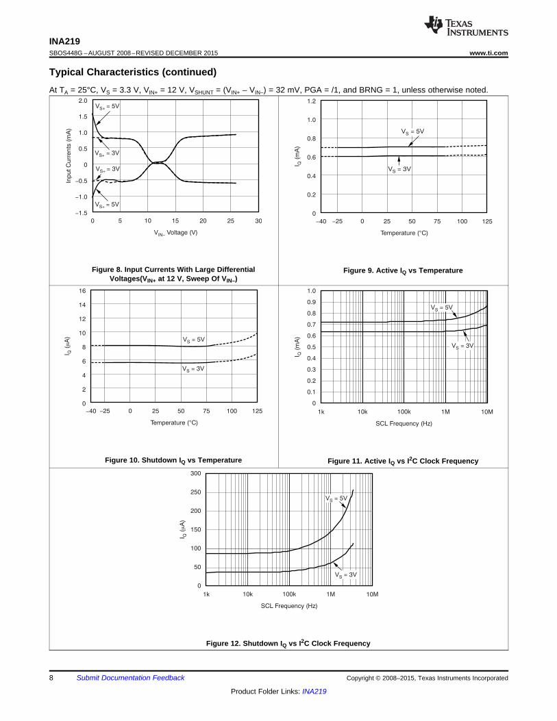
Figure 8. Input Currents With Large Differential Figure 9. Active IQ vs TemperatureVoltages(VIN+ at 12 V, Sweep Of VIN–)
Figure 10. Shutdown IQ vs Temperature Figure 11. Active IQ vs I2C Clock Frequency
Figure 12. Shutdown IQ vs I2C Clock Frequency
8 Submit Documentation Feedback Copyright © 2008–2015, Texas Instruments Incorporated
Product Folder Links: INA219
ADC
´
´
Shunt Voltage
Channel
Bus Voltage
Channel
PGA
(In Configuration Register)
Shunt Voltage(1)
Data Registers
Full-Scale Calibration(2)
Current(1)
Bus Voltage(1)
Power(1)
NOTES:
(1) Read-only
(2) Read/write
INA219www.ti.com SBOS448G –AUGUST 2008–REVISED DECEMBER 2015
8 Detailed Description
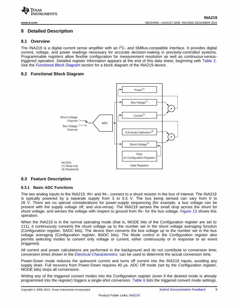
8.1 OverviewThe INA219 is a digital current sense amplifier with an I2C- and SMBus-compatible interface. It provides digitalcurrent, voltage, and power readings necessary for accurate decision-making in precisely-controlled systems.Programmable registers allow flexible configuration for measurement resolution as well as continuous-versus-triggered operation. Detailed register information appears at the end of this data sheet, beginning with Table 2.See the Functional Block Diagram section for a block diagram of the INA219 device.
8.2 Functional Block Diagram
8.3 Feature Description
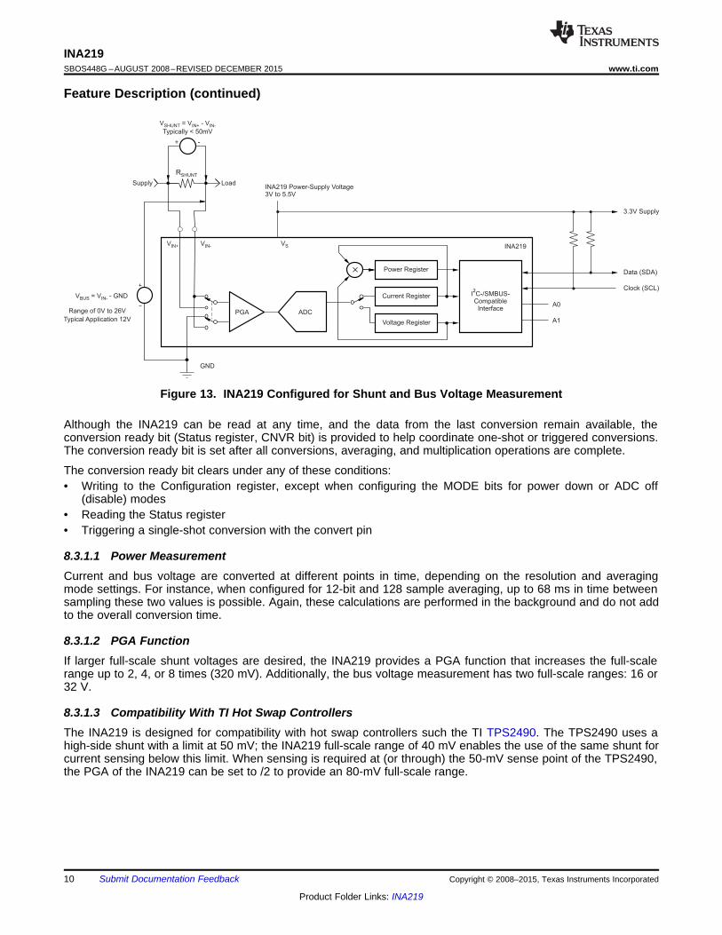
8.3.1 Basic ADC FunctionsThe two analog inputs to the INA219, IN+ and IN–, connect to a shunt resistor in the bus of interest. The INA219is typically powered by a separate supply from 3 to 5.5 V. The bus being sensed can vary from 0 to26 V. There are no special considerations for power-supply sequencing (for example, a bus voltage can bepresent with the supply voltage off, and vice-versa). The INA219 senses the small drop across the shunt forshunt voltage, and senses the voltage with respect to ground from IN– for the bus voltage. Figure 13 shows thisoperation.
When the INA219 is in the normal operating mode (that is, MODE bits of the Configuration register are set to111), it continuously converts the shunt voltage up to the number set in the shunt voltage averaging function(Configuration register, SADC bits). The device then converts the bus voltage up to the number set in the busvoltage averaging (Configuration register, BADC bits). The Mode control in the Configuration register alsopermits selecting modes to convert only voltage or current, either continuously or in response to an event(triggered).
All current and power calculations are performed in the background and do not contribute to conversion time;conversion times shown in the Electrical Characteristics: can be used to determine the actual conversion time.
Power-Down mode reduces the quiescent current and turns off current into the INA219 inputs, avoiding anysupply drain. Full recovery from Power-Down requires 40 μs. ADC Off mode (set by the Configuration register,MODE bits) stops all conversions.
Writing any of the triggered convert modes into the Configuration register (even if the desired mode is alreadyprogrammed into the register) triggers a single-shot conversion. Table 6 lists the triggered convert mode settings.
Copyright © 2008–2015, Texas Instruments Incorporated Submit Documentation Feedback 9
Product Folder Links: INA219
V = V - GNDBUS IN-
Range of 0V to 26V
Typical Application 12V
Data (SDA)
3.3V Supply
Clock (SCL)
´ Power Register
Current Register I C-/SMBUS-Compatible
Interface
2
Voltage Register
VIN+ VIN-
ADCPGA
INA219
GND
A0
A1
V = V - VSHUNT IN+ IN-
Typically < 50mV
Supply Load
-+
INA219 Power-Supply Voltage3V to 5.5V
VS
RSHUNT
INA219SBOS448G –AUGUST 2008–REVISED DECEMBER 2015 www.ti.com
Feature Description (continued)
Figure 13. INA219 Configured for Shunt and Bus Voltage Measurement
Although the INA219 can be read at any time, and the data from the last conversion remain available, theconversion ready bit (Status register, CNVR bit) is provided to help coordinate one-shot or triggered conversions.The conversion ready bit is set after all conversions, averaging, and multiplication operations are complete.
The conversion ready bit clears under any of these conditions:• Writing to the Configuration register, except when configuring the MODE bits for power down or ADC off
(disable) modes• Reading the Status register• Triggering a single-shot conversion with the convert pin
8.3.1.1 Power MeasurementCurrent and bus voltage are converted at different points in time, depending on the resolution and averagingmode settings. For instance, when configured for 12-bit and 128 sample averaging, up to 68 ms in time betweensampling these two values is possible. Again, these calculations are performed in the background and do not addto the overall conversion time.
8.3.1.2 PGA FunctionIf larger full-scale shunt voltages are desired, the INA219 provides a PGA function that increases the full-scalerange up to 2, 4, or 8 times (320 mV). Additionally, the bus voltage measurement has two full-scale ranges: 16 or32 V.
8.3.1.3 Compatibility With TI Hot Swap ControllersThe INA219 is designed for compatibility with hot swap controllers such the TI TPS2490. The TPS2490 uses ahigh-side shunt with a limit at 50 mV; the INA219 full-scale range of 40 mV enables the use of the same shunt forcurrent sensing below this limit. When sensing is required at (or through) the 50-mV sense point of the TPS2490,the PGA of the INA219 can be set to /2 to provide an 80-mV full-scale range.
10 Submit Documentation Feedback Copyright © 2008–2015, Texas Instruments Incorporated
Product Folder Links: INA219
Supply Load
R 10WFILTERR 10WFILTER
0.1 F to 1 Fm m
Ceramic Capacitor
Data (SDA)
3.3V Supply
Clock (SCL)
´ Power Register
Current RegisterI C-/SMBUS-Compatible
Interface
2
Voltage Register
VIN+ VIN-
ADCPGA
INA219
GND
A0
A1
Supply Voltage
VS
RSHUNT
INA219www.ti.com SBOS448G –AUGUST 2008–REVISED DECEMBER 2015
8.4 Device Functional Modes
8.4.1 Filtering and Input ConsiderationsMeasuring current is often noisy, and such noise can be difficult to define. The INA219 offers several options forfiltering by choosing resolution and averaging in the Configuration register. These filtering options can be setindependently for either voltage or current measurement.
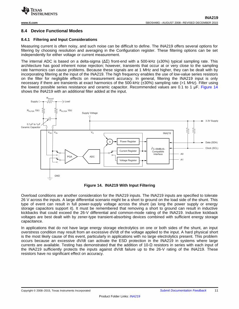
The internal ADC is based on a delta-sigma (ΔΣ) front-end with a 500-kHz (±30%) typical sampling rate. Thisarchitecture has good inherent noise rejection; however, transients that occur at or very close to the samplingrate harmonics can cause problems. Because these signals are at 1 MHz and higher, they can be dealt with byincorporating filtering at the input of the INA219. The high frequency enables the use of low-value series resistorson the filter for negligible effects on measurement accuracy. In general, filtering the INA219 input is onlynecessary if there are transients at exact harmonics of the 500-kHz (±30%) sampling rate (>1 MHz). Filter usingthe lowest possible series resistance and ceramic capacitor. Recommended values are 0.1 to 1 μF. Figure 14shows the INA219 with an additional filter added at the input.
Figure 14. INA219 With Input Filtering
Overload conditions are another consideration for the INA219 inputs. The INA219 inputs are specified to tolerate26 V across the inputs. A large differential scenario might be a short to ground on the load side of the shunt. Thistype of event can result in full power-supply voltage across the shunt (as long the power supply or energystorage capacitors support it). It must be remembered that removing a short to ground can result in inductivekickbacks that could exceed the 26-V differential and common-mode rating of the INA219. Inductive kickbackvoltages are best dealt with by zener-type transient-absorbing devices combined with sufficient energy storagecapacitance.
In applications that do not have large energy storage electrolytics on one or both sides of the shunt, an inputoverstress condition may result from an excessive dV/dt of the voltage applied to the input. A hard physical shortis the most likely cause of this event, particularly in applications with no large electrolytics present. This problemoccurs because an excessive dV/dt can activate the ESD protection in the INA219 in systems where largecurrents are available. Testing has demonstrated that the addition of 10-Ω resistors in series with each input ofthe INA219 sufficiently protects the inputs against dV/dt failure up to the 26-V rating of the INA219. Theseresistors have no significant effect on accuracy.
Copyright © 2008–2015, Texas Instruments Incorporated Submit Documentation Feedback 11
Product Folder Links: INA219
Current Register Bus Voltage RegisterPower Register
5000
´
=
Shunt Voltage Register Calibration RegisterCurrent Register
4096
´
=
Power_LSB = 20 Current_LSB
Maximum Expected Current
215Current_LSB =
Cal = trunc0.04096
Current_LSB R´ SHUNT
INA219SBOS448G –AUGUST 2008–REVISED DECEMBER 2015 www.ti.com
8.5 ProgrammingAn important aspect of the INA219 device is that it measure current or power if it is programmed based on thesystem. The device measures both the differential voltage applied between the IN+ and IN- input pins and thevoltage at IN- pin. In order for the device to report both current and power values, the user must program theresolution of the Current Register (04h) and the value of the shunt resistor (RSHUNT) present in the application todevelop the differential voltage applied between the input pins. Both the Current_LSB and shunt resistor valueare used in the calculation of the Calibration Register value that the device uses to calculate the correspondingcurrent and power values based on the measured shunt and bus voltages.
After programming the Calibration Register, the Current Register (04h) and Power Register (03h) updateaccordingly based on the corresponding shunt voltage and bus voltage measurements. Until the CalibrationRegister is programmed, the Current Register (04h) and Power Register (03h) remain at zero.
8.5.1 Programming the Calibration RegisterThe Calibration Register is calculated based on Equation 1. This equation includes the term Current_LSB, whichis the programmed value for the LSB for the Current Register (04h). The user uses this value to convert thevalue in the Current Register (04h) to the actual current in amperes. The highest resolution for the CurrentRegister (04h) can be obtained by using the smallest allowable Current_LSB based on the maximum expectedcurrent as shown in Equation 2. While this value yields the highest resolution, it is common to select a value forthe Current_LSB to the nearest round number above this value to simplify the conversion of the Current Register(04h) and Power Register (03h) to amperes and watts respectively. The RSHUNT term is the value of the externalshunt used to develop the differential voltage across the input pins. The Power Register (03h) is internally set tobe 20 times the programmed Current_LSB see Equation 3.
where• 0.04096 is an internal fixed value used to ensure scaling is maintained properly (1)
(2)
(3)
Shunt voltage is calculated by multiplying the Shunt Voltage Register contents with the Shunt Voltage LSB of 10µV.
The Bus Voltage register bits are not right-aligned. In order to compute the value of the Bus Voltage, Bus VoltageRegister contents must be shifted right by three bits. This shift puts the BD0 bit in the LSB position so that thecontents can be multiplied by the Bus Voltage LSB of 4-mV to compute the bus voltage measured by the device.
After programming the Calibration Register, the value expected in the Current Register (04h) can be calculatedby multiplying the Shunt Voltage register contents by the Calibration Register and then dividing by 4096 asshown in Equation 4. To obtain a value in amperes the Current register value is multiplied by the programmedCurrent_LSB.
(4)
The value expected in the Power register (03h) can be calculated by multiplying the Current register value by theBus Voltage register value and then dividing by 5000 as shown in Equation 5. Power Register content ismultiplied by Power LSB which is 20 times the Current_LSB for a power value in watts.
(5)
12 Submit Documentation Feedback Copyright © 2008–2015, Texas Instruments Incorporated
Product Folder Links: INA219
Corrected_Full_Scale_Cal = truncCal MeasShuntCurrent
INA219_Current´
INA219www.ti.com SBOS448G –AUGUST 2008–REVISED DECEMBER 2015
Programming (continued)8.5.2 Programming the Power Measurement Engine
8.5.2.1 Calibration Register and ScalingThe Calibration Register enables the user to scale the Current Register (04h) and Power Register (03h) to themost useful value for a given application. For example, set the Calibration Register such that the largest possiblenumber is generated in the Current Register (04h) or Power Register (03h) at the expected full-scale point. Thisapproach yields the highest resolution using the previously calculated minimum Current_LSB in the equation forthe Calibration Register. The Calibration Register can also be selected to provide values in the Current Register(04h) and Power Register (03h) that either provide direct decimal equivalents of the values being measured, oryield a round LSB value for each corresponding register. After these choices have been made, the CalibrationRegister also offers possibilities for end user system-level calibration. After determining the exact current byusing an external ammeter, the value of the Calibration Register can then be adjusted based on the measuredcurrent result of the INA219 to cancel the total system error as shown in Equation 6.
(6)
8.5.3 Simple Current Shunt Monitor Usage (No Programming Necessary)The INA219 can be used without any programming if it is only necessary to read a shunt voltage drop and busvoltage with the default 12-bit resolution, 320-mV shunt full-scale range (PGA = /8), 32-V bus full-scale range,and continuous conversion of shunt and bus voltage.
Without programming, current is measured by reading the shunt voltage. The Current register and Power registerare only available if the Calibration register contains a programmed value.
8.5.4 Default SettingsThe default power-up states of the registers are shown in the Register Details section of this data sheet. Theseregisters are volatile, and if programmed to other than default values, must be re-programmed at every devicepower-up. Detailed information on programming the Calibration register specifically is given in the section,Programming the Calibration Register.
8.5.5 Bus OverviewThe INA219 offers compatibility with both I2C and SMBus interfaces. The I2C and SMBus protocols areessentially compatible with one another.
The I2C interface is used throughout this data sheet as the primary example, with SMBus protocol specified onlywhen a difference between the two systems is being addressed. Two bidirectional lines, SCL and SDA, connectthe INA219 to the bus. Both SCL and SDA are open-drain connections.
The device that initiates the transfer is called a master, and the devices controlled by the master are slaves. Thebus must be controlled by a master device that generates the serial clock (SCL), controls the bus access, andgenerates START and STOP conditions.
To address a specific device, the master initiates a START condition by pulling the data signal line (SDA) from aHIGH to a LOW logic level while SCL is HIGH. All slaves on the bus shift in the slave address byte on the risingedge of SCL, with the last bit indicating whether a read or write operation is intended. During the ninth clockpulse, the slave being addressed responds to the master by generating an Acknowledge and pulling SDA LOW.
Data transfer is then initiated and eight bits of data are sent, followed by an Acknowledge bit. During datatransfer, SDA must remain stable while SCL is HIGH. Any change in SDA while SCL is HIGH is interpreted as aSTART or STOP condition.
Once all data have been transferred, the master generates a STOP condition, indicated by pulling SDA fromLOW to HIGH while SCL is HIGH. The INA219 includes a 28-ms timeout on its interface to prevent locking up anSMBus.
Copyright © 2008–2015, Texas Instruments Incorporated Submit Documentation Feedback 13
Product Folder Links: INA219
INA219SBOS448G –AUGUST 2008–REVISED DECEMBER 2015 www.ti.com
Programming (continued)8.5.5.1 Serial Bus AddressTo communicate with the INA219, the master must first address slave devices through a slave address byte. Theslave address byte consists of seven address bits, and a direction bit indicating the intent of executing a read orwrite operation.
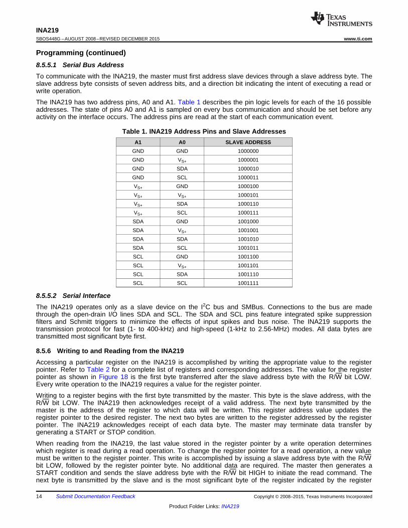
The INA219 has two address pins, A0 and A1. Table 1 describes the pin logic levels for each of the 16 possibleaddresses. The state of pins A0 and A1 is sampled on every bus communication and should be set before anyactivity on the interface occurs. The address pins are read at the start of each communication event.
Table 1. INA219 Address Pins and Slave AddressesA1 A0 SLAVE ADDRESS
GND GND 1000000GND VS+ 1000001GND SDA 1000010GND SCL 1000011VS+ GND 1000100VS+ VS+ 1000101VS+ SDA 1000110VS+ SCL 1000111SDA GND 1001000SDA VS+ 1001001SDA SDA 1001010SDA SCL 1001011SCL GND 1001100SCL VS+ 1001101SCL SDA 1001110SCL SCL 1001111
8.5.5.2 Serial InterfaceThe INA219 operates only as a slave device on the I2C bus and SMBus. Connections to the bus are madethrough the open-drain I/O lines SDA and SCL. The SDA and SCL pins feature integrated spike suppressionfilters and Schmitt triggers to minimize the effects of input spikes and bus noise. The INA219 supports thetransmission protocol for fast (1- to 400-kHz) and high-speed (1-kHz to 2.56-MHz) modes. All data bytes aretransmitted most significant byte first.
8.5.6 Writing to and Reading from the INA219Accessing a particular register on the INA219 is accomplished by writing the appropriate value to the registerpointer. Refer to Table 2 for a complete list of registers and corresponding addresses. The value for the registerpointer as shown in Figure 18 is the first byte transferred after the slave address byte with the R/W bit LOW.Every write operation to the INA219 requires a value for the register pointer.
Writing to a register begins with the first byte transmitted by the master. This byte is the slave address, with theR/W bit LOW. The INA219 then acknowledges receipt of a valid address. The next byte transmitted by themaster is the address of the register to which data will be written. This register address value updates theregister pointer to the desired register. The next two bytes are written to the register addressed by the registerpointer. The INA219 acknowledges receipt of each data byte. The master may terminate data transfer bygenerating a START or STOP condition.
When reading from the INA219, the last value stored in the register pointer by a write operation determineswhich register is read during a read operation. To change the register pointer for a read operation, a new valuemust be written to the register pointer. This write is accomplished by issuing a slave address byte with the R/Wbit LOW, followed by the register pointer byte. No additional data are required. The master then generates aSTART condition and sends the slave address byte with the R/W bit HIGH to initiate the read command. Thenext byte is transmitted by the slave and is the most significant byte of the register indicated by the register
14 Submit Documentation Feedback Copyright © 2008–2015, Texas Instruments Incorporated
Product Folder Links: INA219

INA219www.ti.com SBOS448G –AUGUST 2008–REVISED DECEMBER 2015
pointer. This byte is followed by an Acknowledge from the master; then the slave transmits the least significantbyte. The master acknowledges receipt of the data byte. The master may terminate data transfer by generating aNot-Acknowledge after receiving any data byte, or generating a START or STOP condition. If repeated readsfrom the same register are desired, it is not necessary to continually send the register pointer bytes; the INA219retains the register pointer value until it is changed by the next write operation.
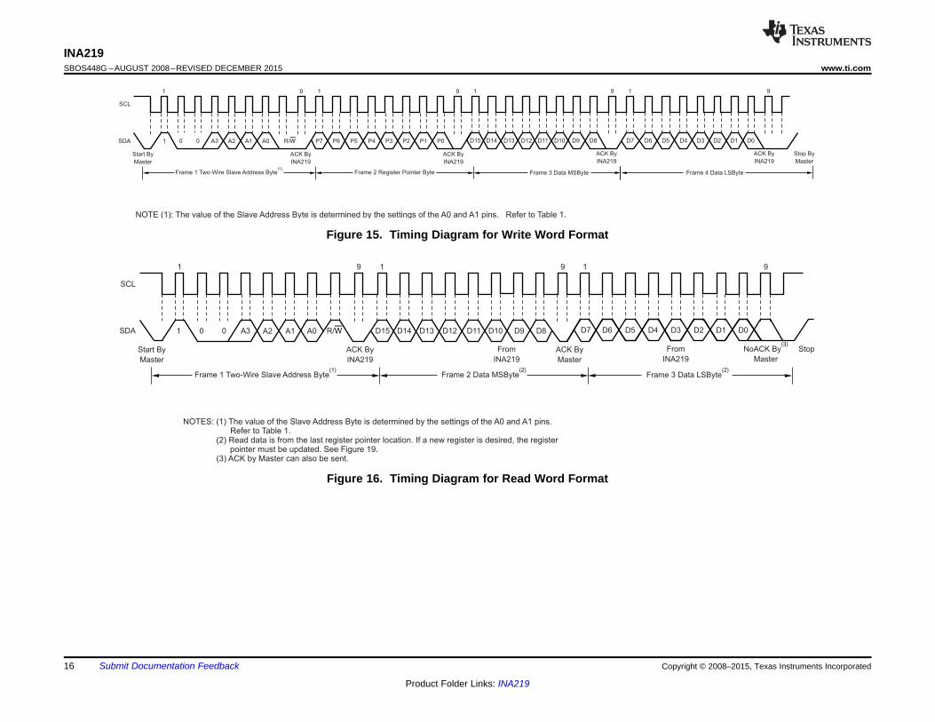
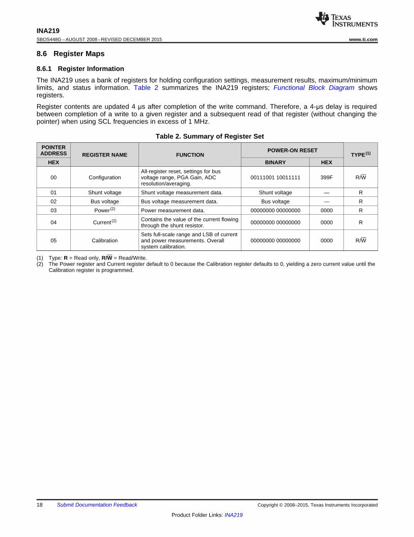
Figure 15 and Figure 16 show write and read operation timing diagrams, respectively. Note that register bytesare sent most-significant byte first, followed by the least significant byte. Figure 17 shows the timing diagram forthe SMBus Alert response operation. Figure 18 shows a typical register pointer configuration.
Copyright © 2008–2015, Texas Instruments Incorporated Submit Documentation Feedback 15
Product Folder Links: INA219
Frame 1 Two-Wire Slave Address Byte(1)
Frame 2 Data MSByte(2)
1
Start By
Master
ACK By
INA219
ACK By
Master
From
INA219
1 9 1 9
SDA
SCL
0 0 A3 R/W D15 D14 D13 D12 D11 D10 D9 D8A2 A1 A0
Frame 3 Data LSByte(2)
StopNoACK By(3)
Master
From
INA219
1 9
D7 D6 D5 D4 D3 D2 D1 D0
NOTES: (1) The value of the Slave Address Byte is determined by the settings of the A0 and A1 pins.Refer to Table 1.
(2) Read data is from the last register pointer location. If a new register is desired, the registerpointer must be updated. See Figure 19.
(3) ACK by Master can also be sent.
Frame 1 Two-Wire Slave Address Byte(1)
Frame 2 Register Pointer Byte
Start By
Master
ACK By
INA219
ACK By
INA219
1 9 1
ACK By
INA219
1
D15 D14 D13 D12 D11 D10 D9 D8
99
SDA
SCL
1 0 0 A3 A2 A1 A0 R/W P7 P6 P5 P4 P3 P2 P1 P0
NOTE (1): The value of the Slave Address Byte is determined by the settings of the A0 and A1 pins. Refer to Table 1.
Frame 4 Data LSByteFrame 3 Data MSByte
ACK By
INA219
Stop By
Master
1
D7 D6 D5 D4 D3 D2 D1 D0
9
INA219SBOS448G –AUGUST 2008–REVISED DECEMBER 2015 www.ti.com
Figure 15. Timing Diagram for Write Word Format
Figure 16. Timing Diagram for Read Word Format
16 Submit Documentation Feedback Copyright © 2008–2015, Texas Instruments Incorporated
Product Folder Links: INA219
Frame 1 Two-Wire Slave Address Byte(1)
Frame 2 Register Pointer Byte
1
Start By
Master
ACK By
INA219
ACK By
INA219
1 9 1 9
SDA
SCL
0 0 A3 A2 A1 A0 R/W P7 P6 P5 P4 P3 P2 P1 P0 Stop
¼
NOTE (1): The value of the Slave Address Byte is determined by the settings of the A0 and A1 pins. Refer to Table 1.
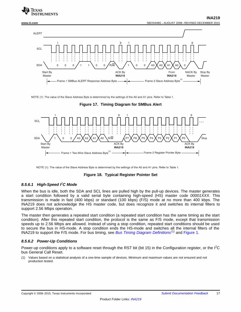
Frame 1 SMBus ALERT Response Address Byte Frame 2 Slave Address Byte(1)
Start By
Master
ACK By
INA219
From
INA219
NACK By
Master
Stop By
Master
1 9 1 9
SDA
SCL
ALERT
0 0 0 1 1 0 0 R/W 1 0 0 A3 A2 A1 A0 0
NOTE (1): The value of the Slave Address Byte is determined by the settings of the A0 and A1 pins. Refer to Table 1.
INA219www.ti.com SBOS448G –AUGUST 2008–REVISED DECEMBER 2015
Figure 17. Timing Diagram for SMBus Alert
Figure 18. Typical Register Pointer Set
8.5.6.1 High-Speed I2C ModeWhen the bus is idle, both the SDA and SCL lines are pulled high by the pull-up devices. The master generatesa start condition followed by a valid serial byte containing high-speed (HS) master code 00001XXX. Thistransmission is made in fast (400 kbps) or standard (100 kbps) (F/S) mode at no more than 400 kbps. TheINA219 does not acknowledge the HS master code, but does recognize it and switches its internal filters tosupport 2.56 Mbps operation.
The master then generates a repeated start condition (a repeated start condition has the same timing as the startcondition). After this repeated start condition, the protocol is the same as F/S mode, except that transmissionspeeds up to 2.56 Mbps are allowed. Instead of using a stop condition, repeated start conditions should be usedto secure the bus in HS-mode. A stop condition ends the HS-mode and switches all the internal filters of theINA219 to support the F/S mode. For bus timing, see Bus Timing Diagram Definitions (1) and Figure 1.
8.5.6.2 Power-Up ConditionsPower-up conditions apply to a software reset through the RST bit (bit 15) in the Configuration register, or the I2Cbus General Call Reset.(1) Values based on a statistical analysis of a one-time sample of devices. Minimum and maximum values are not ensured and not
production tested.
Copyright © 2008–2015, Texas Instruments Incorporated Submit Documentation Feedback 17
Product Folder Links: INA219
INA219SBOS448G –AUGUST 2008–REVISED DECEMBER 2015 www.ti.com
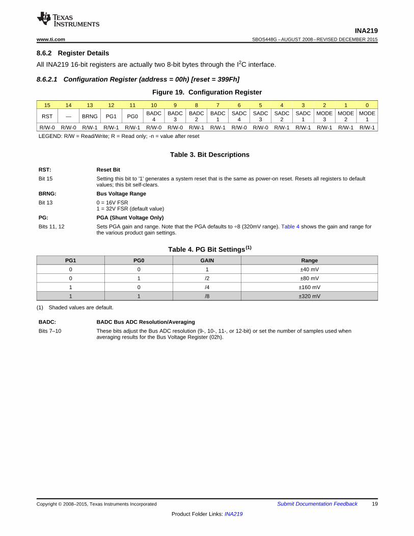
8.6 Register Maps
8.6.1 Register InformationThe INA219 uses a bank of registers for holding configuration settings, measurement results, maximum/minimumlimits, and status information. Table 2 summarizes the INA219 registers; Functional Block Diagram showsregisters.
Register contents are updated 4 μs after completion of the write command. Therefore, a 4-μs delay is requiredbetween completion of a write to a given register and a subsequent read of that register (without changing thepointer) when using SCL frequencies in excess of 1 MHz.
Table 2. Summary of Register SetPOINTER POWER-ON RESETADDRESS REGISTER NAME FUNCTION TYPE (1)
HEX BINARY HEXAll-register reset, settings for bus
00 Configuration voltage range, PGA Gain, ADC 00111001 10011111 399F R/Wresolution/averaging.
01 Shunt voltage Shunt voltage measurement data. Shunt voltage — R02 Bus voltage Bus voltage measurement data. Bus voltage — R03 Power (2) Power measurement data. 00000000 00000000 0000 R
Contains the value of the current flowing04 Current (2) 00000000 00000000 0000 Rthrough the shunt resistor.Sets full-scale range and LSB of current
05 Calibration and power measurements. Overall 00000000 00000000 0000 R/Wsystem calibration.
(1) Type: R = Read only, R/W = Read/Write.(2) The Power register and Current register default to 0 because the Calibration register defaults to 0, yielding a zero current value until the
Calibration register is programmed.
18 Submit Documentation Feedback Copyright © 2008–2015, Texas Instruments Incorporated
Product Folder Links: INA219
INA219www.ti.com SBOS448G –AUGUST 2008–REVISED DECEMBER 2015
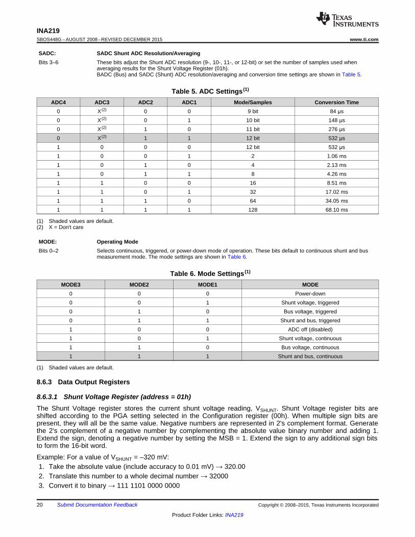
8.6.2 Register DetailsAll INA219 16-bit registers are actually two 8-bit bytes through the I2C interface.
8.6.2.1 Configuration Register (address = 00h) [reset = 399Fh]
Figure 19. Configuration Register
15 14 13 12 11 10 9 8 7 6 5 4 3 2 1 0BADC BADC BADC BADC SADC SADC SADC SADC MODE MODE MODERST — BRNG PG1 PG0 4 3 2 1 4 3 2 1 3 2 1
R/W-0 R/W-0 R/W-1 R/W-1 R/W-1 R/W-0 R/W-0 R/W-1 R/W-1 R/W-0 R/W-0 R/W-1 R/W-1 R/W-1 R/W-1 R/W-1LEGEND: R/W = Read/Write; R = Read only; -n = value after reset
Table 3. Bit Descriptions
RST: Reset BitBit 15 Setting this bit to '1' generates a system reset that is the same as power-on reset. Resets all registers to default
values; this bit self-clears.BRNG: Bus Voltage RangeBit 13 0 = 16V FSR
1 = 32V FSR (default value)PG: PGA (Shunt Voltage Only)Bits 11, 12 Sets PGA gain and range. Note that the PGA defaults to ÷8 (320mV range). Table 4 shows the gain and range for
the various product gain settings.
Table 4. PG Bit Settings (1)
PG1 PG0 GAIN Range0 0 1 ±40 mV0 1 /2 ±80 mV1 0 /4 ±160 mV1 1 /8 ±320 mV
(1) Shaded values are default.
BADC: BADC Bus ADC Resolution/AveragingBits 7–10 These bits adjust the Bus ADC resolution (9-, 10-, 11-, or 12-bit) or set the number of samples used when
averaging results for the Bus Voltage Register (02h).
Copyright © 2008–2015, Texas Instruments Incorporated Submit Documentation Feedback 19
Product Folder Links: INA219
INA219SBOS448G –AUGUST 2008–REVISED DECEMBER 2015 www.ti.com
SADC: SADC Shunt ADC Resolution/AveragingBits 3–6 These bits adjust the Shunt ADC resolution (9-, 10-, 11-, or 12-bit) or set the number of samples used when
averaging results for the Shunt Voltage Register (01h).BADC (Bus) and SADC (Shunt) ADC resolution/averaging and conversion time settings are shown in Table 5.
Table 5. ADC Settings (1)
ADC4 ADC3 ADC2 ADC1 Mode/Samples Conversion Time0 X (2) 0 0 9 bit 84 μs0 X (2) 0 1 10 bit 148 μs0 X (2) 1 0 11 bit 276 μs0 X (2) 1 1 12 bit 532 μs1 0 0 0 12 bit 532 μs1 0 0 1 2 1.06 ms1 0 1 0 4 2.13 ms1 0 1 1 8 4.26 ms1 1 0 0 16 8.51 ms1 1 0 1 32 17.02 ms1 1 1 0 64 34.05 ms1 1 1 1 128 68.10 ms
(1) Shaded values are default.(2) X = Don't care
MODE: Operating ModeBits 0–2 Selects continuous, triggered, or power-down mode of operation. These bits default to continuous shunt and bus
measurement mode. The mode settings are shown in Table 6.
Table 6. Mode Settings (1)
MODE3 MODE2 MODE1 MODE0 0 0 Power-down0 0 1 Shunt voltage, triggered0 1 0 Bus voltage, triggered0 1 1 Shunt and bus, triggered1 0 0 ADC off (disabled)1 0 1 Shunt voltage, continuous1 1 0 Bus voltage, continuous1 1 1 Shunt and bus, continuous
(1) Shaded values are default.
8.6.3 Data Output Registers
8.6.3.1 Shunt Voltage Register (address = 01h)The Shunt Voltage register stores the current shunt voltage reading, VSHUNT. Shunt Voltage register bits areshifted according to the PGA setting selected in the Configuration register (00h). When multiple sign bits arepresent, they will all be the same value. Negative numbers are represented in 2's complement format. Generatethe 2's complement of a negative number by complementing the absolute value binary number and adding 1.Extend the sign, denoting a negative number by setting the MSB = 1. Extend the sign to any additional sign bitsto form the 16-bit word.
Example: For a value of VSHUNT = –320 mV:1. Take the absolute value (include accuracy to 0.01 mV) → 320.002. Translate this number to a whole decimal number → 320003. Convert it to binary → 111 1101 0000 0000
20 Submit Documentation Feedback Copyright © 2008–2015, Texas Instruments Incorporated
Product Folder Links: INA219
INA219www.ti.com SBOS448G –AUGUST 2008–REVISED DECEMBER 2015
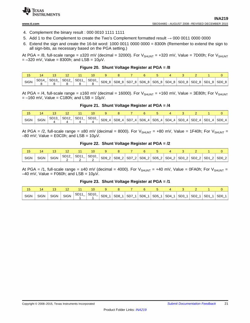
4. Complement the binary result : 000 0010 1111 11115. Add 1 to the Complement to create the Two’s Complement formatted result → 000 0011 0000 00006. Extend the sign and create the 16-bit word: 1000 0011 0000 0000 = 8300h (Remember to extend the sign to
all sign-bits, as necessary based on the PGA setting.)
At PGA = /8, full-scale range = ±320 mV (decimal = 32000). For VSHUNT = +320 mV, Value = 7D00h; For VSHUNT= –320 mV, Value = 8300h; and LSB = 10µV.
Figure 20. Shunt Voltage Register at PGA = /8
15 14 13 12 11 10 9 8 7 6 5 4 3 2 1 0SD14_ SD13_ SD12_ SD11_ SD10_SIGN SD9_8 SD8_8 SD7_8 SD6_8 SD5_8 SD4_8 SD3_8 SD2_8 SD1_8 SD0_88 8 8 8 8
At PGA = /4, full-scale range = ±160 mV (decimal = 16000). For VSHUNT = +160 mV, Value = 3E80h; For VSHUNT= –160 mV, Value = C180h; and LSB = 10µV.
Figure 21. Shunt Voltage Register at PGA = /4
15 14 13 12 11 10 9 8 7 6 5 4 3 2 1 0SD13_ SD12_ SD11_ SD10_SIGN SIGN SD9_4 SD8_4 SD7_4 SD6_4 SD5_4 SD4_4 SD3_4 SD2_4 SD1_4 SD0_44 4 4 4
At PGA = /2, full-scale range = ±80 mV (decimal = 8000). For VSHUNT = +80 mV, Value = 1F40h; For VSHUNT =–80 mV; Value = E0C0h; and LSB = 10µV.
Figure 22. Shunt Voltage Register at PGA = /2
15 14 13 12 11 10 9 8 7 6 5 4 3 2 1 0SD12_ SD11_ SD10_SIGN SIGN SIGN SD9_2 SD8_2 SD7_2 SD6_2 SD5_2 SD4_2 SD3_2 SD2_2 SD1_2 SD0_22 2 2
At PGA = /1, full-scale range = ±40 mV (decimal = 4000). For VSHUNT = +40 mV, Value = 0FA0h; For VSHUNT =–40 mV, Value = F060h; and LSB = 10µV.
Figure 23. Shunt Voltage Register at PGA = /1
15 14 13 12 11 10 9 8 7 6 5 4 3 2 1 0SD11_ SD10_SIGN SIGN SIGN SIGN SD9_1 SD8_1 SD7_1 SD6_1 SD5_1 SD4_1 SD3_1 SD2_1 SD1_1 SD0_11 1
Copyright © 2008–2015, Texas Instruments Incorporated Submit Documentation Feedback 21
Product Folder Links: INA219
INA219SBOS448G –AUGUST 2008–REVISED DECEMBER 2015 www.ti.com
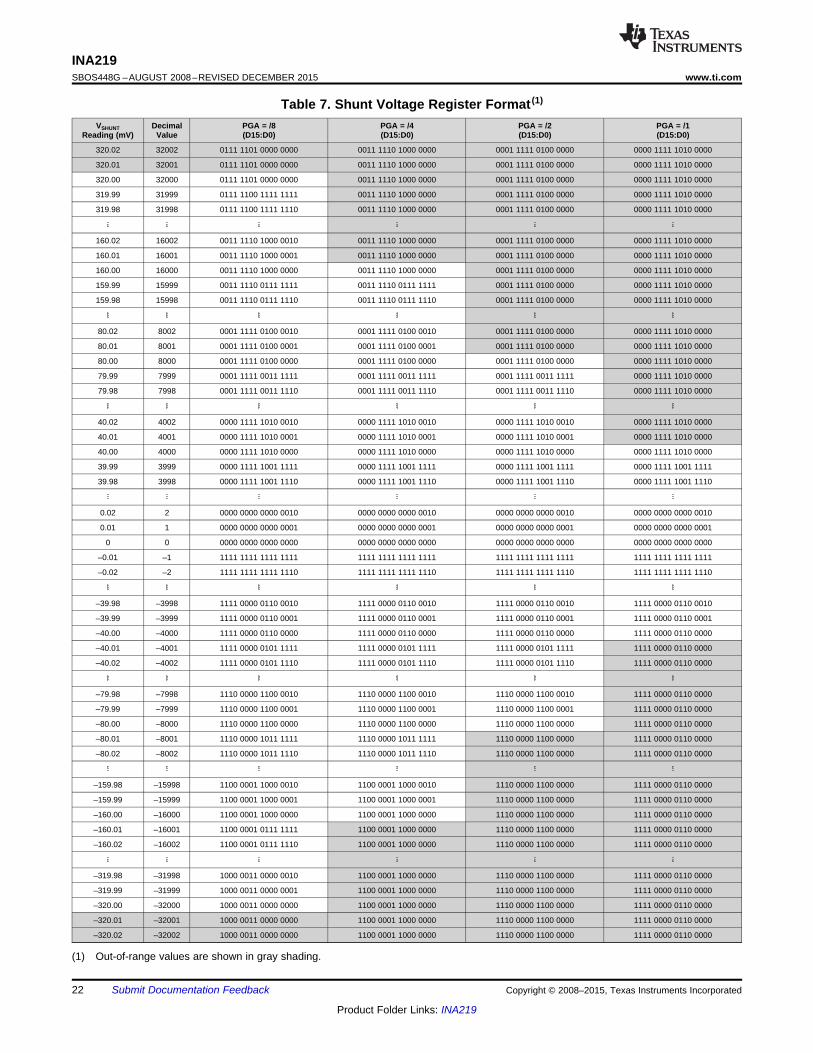
Table 7. Shunt Voltage Register Format (1)
VSHUNT Decimal PGA = /8 PGA = /4 PGA = /2 PGA = /1Reading (mV) Value (D15:D0) (D15:D0) (D15:D0) (D15:D0)
320.02 32002 0111 1101 0000 0000 0011 1110 1000 0000 0001 1111 0100 0000 0000 1111 1010 0000
320.01 32001 0111 1101 0000 0000 0011 1110 1000 0000 0001 1111 0100 0000 0000 1111 1010 0000
320.00 32000 0111 1101 0000 0000 0011 1110 1000 0000 0001 1111 0100 0000 0000 1111 1010 0000
319.99 31999 0111 1100 1111 1111 0011 1110 1000 0000 0001 1111 0100 0000 0000 1111 1010 0000
319.98 31998 0111 1100 1111 1110 0011 1110 1000 0000 0001 1111 0100 0000 0000 1111 1010 0000
160.02 16002 0011 1110 1000 0010 0011 1110 1000 0000 0001 1111 0100 0000 0000 1111 1010 0000
160.01 16001 0011 1110 1000 0001 0011 1110 1000 0000 0001 1111 0100 0000 0000 1111 1010 0000
160.00 16000 0011 1110 1000 0000 0011 1110 1000 0000 0001 1111 0100 0000 0000 1111 1010 0000
159.99 15999 0011 1110 0111 1111 0011 1110 0111 1111 0001 1111 0100 0000 0000 1111 1010 0000
159.98 15998 0011 1110 0111 1110 0011 1110 0111 1110 0001 1111 0100 0000 0000 1111 1010 0000
80.02 8002 0001 1111 0100 0010 0001 1111 0100 0010 0001 1111 0100 0000 0000 1111 1010 0000
80.01 8001 0001 1111 0100 0001 0001 1111 0100 0001 0001 1111 0100 0000 0000 1111 1010 0000
80.00 8000 0001 1111 0100 0000 0001 1111 0100 0000 0001 1111 0100 0000 0000 1111 1010 0000
79.99 7999 0001 1111 0011 1111 0001 1111 0011 1111 0001 1111 0011 1111 0000 1111 1010 0000
79.98 7998 0001 1111 0011 1110 0001 1111 0011 1110 0001 1111 0011 1110 0000 1111 1010 0000
40.02 4002 0000 1111 1010 0010 0000 1111 1010 0010 0000 1111 1010 0010 0000 1111 1010 0000
40.01 4001 0000 1111 1010 0001 0000 1111 1010 0001 0000 1111 1010 0001 0000 1111 1010 0000
40.00 4000 0000 1111 1010 0000 0000 1111 1010 0000 0000 1111 1010 0000 0000 1111 1010 0000
39.99 3999 0000 1111 1001 1111 0000 1111 1001 1111 0000 1111 1001 1111 0000 1111 1001 1111
39.98 3998 0000 1111 1001 1110 0000 1111 1001 1110 0000 1111 1001 1110 0000 1111 1001 1110
0.02 2 0000 0000 0000 0010 0000 0000 0000 0010 0000 0000 0000 0010 0000 0000 0000 0010
0.01 1 0000 0000 0000 0001 0000 0000 0000 0001 0000 0000 0000 0001 0000 0000 0000 0001
0 0 0000 0000 0000 0000 0000 0000 0000 0000 0000 0000 0000 0000 0000 0000 0000 0000
–0.01 –1 1111 1111 1111 1111 1111 1111 1111 1111 1111 1111 1111 1111 1111 1111 1111 1111
–0.02 –2 1111 1111 1111 1110 1111 1111 1111 1110 1111 1111 1111 1110 1111 1111 1111 1110
–39.98 –3998 1111 0000 0110 0010 1111 0000 0110 0010 1111 0000 0110 0010 1111 0000 0110 0010
–39.99 –3999 1111 0000 0110 0001 1111 0000 0110 0001 1111 0000 0110 0001 1111 0000 0110 0001
–40.00 –4000 1111 0000 0110 0000 1111 0000 0110 0000 1111 0000 0110 0000 1111 0000 0110 0000
–40.01 –4001 1111 0000 0101 1111 1111 0000 0101 1111 1111 0000 0101 1111 1111 0000 0110 0000
–40.02 –4002 1111 0000 0101 1110 1111 0000 0101 1110 1111 0000 0101 1110 1111 0000 0110 0000
–79.98 –7998 1110 0000 1100 0010 1110 0000 1100 0010 1110 0000 1100 0010 1111 0000 0110 0000
–79.99 –7999 1110 0000 1100 0001 1110 0000 1100 0001 1110 0000 1100 0001 1111 0000 0110 0000
–80.00 –8000 1110 0000 1100 0000 1110 0000 1100 0000 1110 0000 1100 0000 1111 0000 0110 0000
–80.01 –8001 1110 0000 1011 1111 1110 0000 1011 1111 1110 0000 1100 0000 1111 0000 0110 0000
–80.02 –8002 1110 0000 1011 1110 1110 0000 1011 1110 1110 0000 1100 0000 1111 0000 0110 0000
–159.98 –15998 1100 0001 1000 0010 1100 0001 1000 0010 1110 0000 1100 0000 1111 0000 0110 0000
–159.99 –15999 1100 0001 1000 0001 1100 0001 1000 0001 1110 0000 1100 0000 1111 0000 0110 0000
–160.00 –16000 1100 0001 1000 0000 1100 0001 1000 0000 1110 0000 1100 0000 1111 0000 0110 0000
–160.01 –16001 1100 0001 0111 1111 1100 0001 1000 0000 1110 0000 1100 0000 1111 0000 0110 0000
–160.02 –16002 1100 0001 0111 1110 1100 0001 1000 0000 1110 0000 1100 0000 1111 0000 0110 0000
–319.98 –31998 1000 0011 0000 0010 1100 0001 1000 0000 1110 0000 1100 0000 1111 0000 0110 0000
–319.99 –31999 1000 0011 0000 0001 1100 0001 1000 0000 1110 0000 1100 0000 1111 0000 0110 0000
–320.00 –32000 1000 0011 0000 0000 1100 0001 1000 0000 1110 0000 1100 0000 1111 0000 0110 0000
–320.01 –32001 1000 0011 0000 0000 1100 0001 1000 0000 1110 0000 1100 0000 1111 0000 0110 0000
–320.02 –32002 1000 0011 0000 0000 1100 0001 1000 0000 1110 0000 1100 0000 1111 0000 0110 0000
(1) Out-of-range values are shown in gray shading.
22 Submit Documentation Feedback Copyright © 2008–2015, Texas Instruments Incorporated
Product Folder Links: INA219
INA219www.ti.com SBOS448G –AUGUST 2008–REVISED DECEMBER 2015
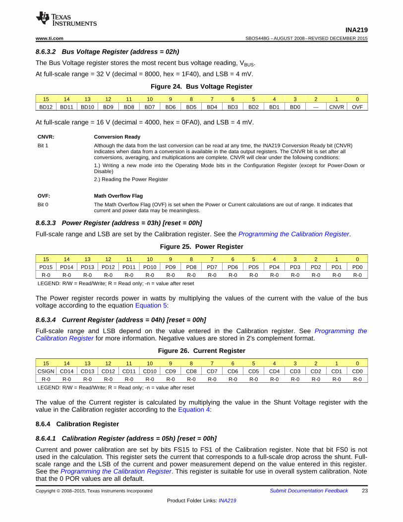
8.6.3.2 Bus Voltage Register (address = 02h)The Bus Voltage register stores the most recent bus voltage reading, VBUS.
At full-scale range = 32 V (decimal = 8000, hex = 1F40), and LSB = 4 mV.
Figure 24. Bus Voltage Register
15 14 13 12 11 10 9 8 7 6 5 4 3 2 1 0BD12 BD11 BD10 BD9 BD8 BD7 BD6 BD5 BD4 BD3 BD2 BD1 BD0 — CNVR OVF
At full-scale range = 16 V (decimal = 4000, hex = 0FA0), and LSB = 4 mV.
CNVR: Conversion ReadyBit 1 Although the data from the last conversion can be read at any time, the INA219 Conversion Ready bit (CNVR)
indicates when data from a conversion is available in the data output registers. The CNVR bit is set after allconversions, averaging, and multiplications are complete. CNVR will clear under the following conditions:1.) Writing a new mode into the Operating Mode bits in the Configuration Register (except for Power-Down orDisable)2.) Reading the Power Register
OVF: Math Overflow FlagBit 0 The Math Overflow Flag (OVF) is set when the Power or Current calculations are out of range. It indicates that
current and power data may be meaningless.
8.6.3.3 Power Register (address = 03h) [reset = 00h]Full-scale range and LSB are set by the Calibration register. See the Programming the Calibration Register.
Figure 25. Power Register
15 14 13 12 11 10 9 8 7 6 5 4 3 2 1 0PD15 PD14 PD13 PD12 PD11 PD10 PD9 PD8 PD7 PD6 PD5 PD4 PD3 PD2 PD1 PD0R-0 R-0 R-0 R-0 R-0 R-0 R-0 R-0 R-0 R-0 R-0 R-0 R-0 R-0 R-0 R-0
LEGEND: R/W = Read/Write; R = Read only; -n = value after reset
The Power register records power in watts by multiplying the values of the current with the value of the busvoltage according to the equation Equation 5:
8.6.3.4 Current Register (address = 04h) [reset = 00h]Full-scale range and LSB depend on the value entered in the Calibration register. See Programming theCalibration Register for more information. Negative values are stored in 2's complement format.
Figure 26. Current Register
15 14 13 12 11 10 9 8 7 6 5 4 3 2 1 0CSIGN CD14 CD13 CD12 CD11 CD10 CD9 CD8 CD7 CD6 CD5 CD4 CD3 CD2 CD1 CD0
R-0 R-0 R-0 R-0 R-0 R-0 R-0 R-0 R-0 R-0 R-0 R-0 R-0 R-0 R-0 R-0LEGEND: R/W = Read/Write; R = Read only; -n = value after reset
The value of the Current register is calculated by multiplying the value in the Shunt Voltage register with thevalue in the Calibration register according to the Equation 4:
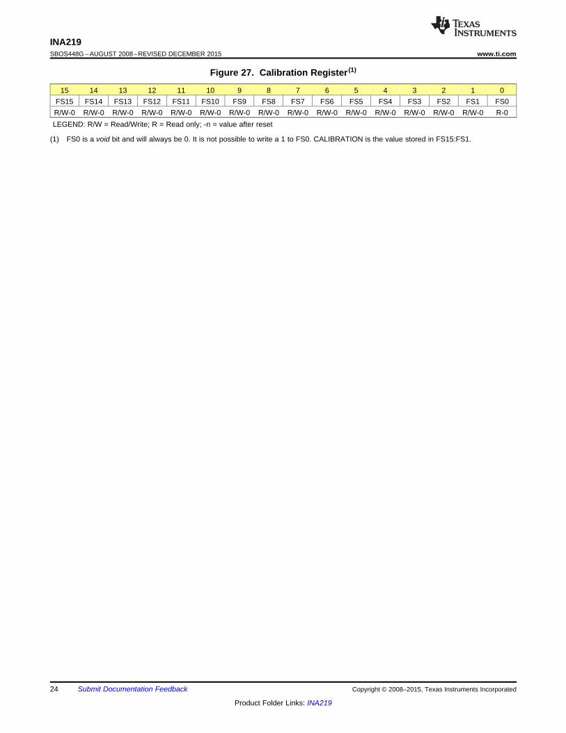
8.6.4 Calibration Register
8.6.4.1 Calibration Register (address = 05h) [reset = 00h]Current and power calibration are set by bits FS15 to FS1 of the Calibration register. Note that bit FS0 is notused in the calculation. This register sets the current that corresponds to a full-scale drop across the shunt. Full-scale range and the LSB of the current and power measurement depend on the value entered in this register.See the Programming the Calibration Register. This register is suitable for use in overall system calibration. Notethat the 0 POR values are all default.
Copyright © 2008–2015, Texas Instruments Incorporated Submit Documentation Feedback 23
Product Folder Links: INA219
INA219SBOS448G –AUGUST 2008–REVISED DECEMBER 2015 www.ti.com
Figure 27. Calibration Register (1)
15 14 13 12 11 10 9 8 7 6 5 4 3 2 1 0FS15 FS14 FS13 FS12 FS11 FS10 FS9 FS8 FS7 FS6 FS5 FS4 FS3 FS2 FS1 FS0R/W-0 R/W-0 R/W-0 R/W-0 R/W-0 R/W-0 R/W-0 R/W-0 R/W-0 R/W-0 R/W-0 R/W-0 R/W-0 R/W-0 R/W-0 R-0LEGEND: R/W = Read/Write; R = Read only; -n = value after reset
(1) FS0 is a void bit and will always be 0. It is not possible to write a 1 to FS0. CALIBRATION is the value stored in FS15:FS1.
24 Submit Documentation Feedback Copyright © 2008–2015, Texas Instruments Incorporated
Product Folder Links: INA219
CBYPASS
0.1 F(typical)
m
Supply Voltage(INA219 Power Supply Range is3V to 5.5V)
Data (SDA)
Clock (SCL)
´ Power Register
Current Register I CInterface
2
Voltage Register
VIN+
RF1 RF2
RPULLUP
3.3k(typical)
W
RPULLUP
3.3k(typical)
WVIN-
ADCPGA
INA219
GND
Power Bus(0V to 26V)
Load
CF
A0
A1
SDA
SCL
RSHUNT
INA219www.ti.com SBOS448G –AUGUST 2008–REVISED DECEMBER 2015
9 Application and Implementation
NOTEInformation in the following applications sections is not part of the TI componentspecification, and TI does not warrant its accuracy or completeness. TI’s customers areresponsible for determining suitability of components for their purposes. Customers shouldvalidate and test their design implementation to confirm system functionality.
9.1 Application InformationThe INA219 is a current shunt and power monitor with an I2C- and SMBus-compatible interface. The devicemonitors both a shunt voltage drop and bus supply voltage. Programmable calibration value, combined with aninternal multiplier, enable readouts of current and power.
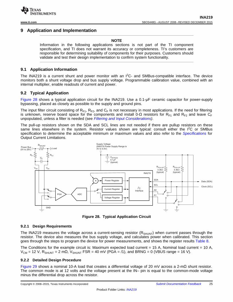
9.2 Typical ApplicationFigure 28 shows a typical application circuit for the INA219. Use a 0.1-μF ceramic capacitor for power-supplybypassing, placed as closely as possible to the supply and ground pins.
The input filter circuit consisting of RF1, RF2, and CF is not necessary in most applications. If the need for filteringis unknown, reserve board space for the components and install 0-Ω resistors for RF1 and RF2 and leave CFunpopulated, unless a filter is needed (see Filtering and Input Considerations).
The pull-up resistors shown on the SDA and SCL lines are not needed if there are pullup resistors on thesesame lines elsewhere in the system. Resistor values shown are typical: consult either the I2C or SMBusspecification to determine the acceptable minimum or maximum values and also refer to the Specifications forOutput Current Limitations.
Figure 28. Typical Application Circuit
9.2.1 Design RequirementsThe INA219 measures the voltage across a current-sensing resistor (RSHUNT) when current passes through theresistor. The device also measures the bus supply voltage, and calculates power when calibrated. This sectiongoes through the steps to program the device for power measurements, and shows the register results Table 8.
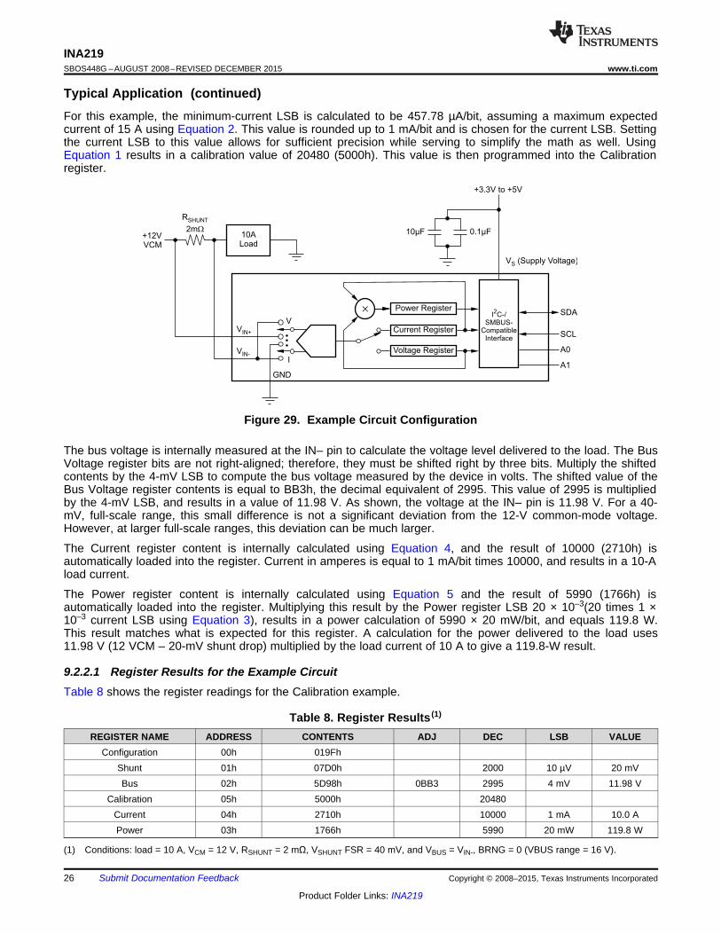
The Conditions for the example circuit is: Maximum expected load current = 15 A, Nominal load current = 10 A,VCM = 12 V, RSHUNT = 2 mΩ, VSHUNT FSR = 40 mV (PGA = /1), and BRNG = 0 (VBUS range = 16 V).
9.2.2 Detailed Design ProcedureFigure 29 shows a nominal 10-A load that creates a differential voltage of 20 mV across a 2-mΩ shunt resistor.The common mode is at 12 volts and the voltage present at the IN– pin is equal to the common-mode voltageminus the differential drop across the resistor.
Copyright © 2008–2015, Texas Instruments Incorporated Submit Documentation Feedback 25
Product Folder Links: INA219
R
2mW
SHUNT
10ALoad
+12VVCM
GND
V
I
VIN+
VIN-
Power RegisterI C-/
SMBUS-Compatible
Interface
2
Current Register
Voltage Register
SDA
SCL
A0
A1
0.1µF10µF
+3.3V to +5V
V (Supply Voltage)S
´
INA219SBOS448G –AUGUST 2008–REVISED DECEMBER 2015 www.ti.com
Typical Application (continued)For this example, the minimum-current LSB is calculated to be 457.78 µA/bit, assuming a maximum expectedcurrent of 15 A using Equation 2. This value is rounded up to 1 mA/bit and is chosen for the current LSB. Settingthe current LSB to this value allows for sufficient precision while serving to simplify the math as well. UsingEquation 1 results in a calibration value of 20480 (5000h). This value is then programmed into the Calibrationregister.
Figure 29. Example Circuit Configuration
The bus voltage is internally measured at the IN– pin to calculate the voltage level delivered to the load. The BusVoltage register bits are not right-aligned; therefore, they must be shifted right by three bits. Multiply the shiftedcontents by the 4-mV LSB to compute the bus voltage measured by the device in volts. The shifted value of theBus Voltage register contents is equal to BB3h, the decimal equivalent of 2995. This value of 2995 is multipliedby the 4-mV LSB, and results in a value of 11.98 V. As shown, the voltage at the IN– pin is 11.98 V. For a 40-mV, full-scale range, this small difference is not a significant deviation from the 12-V common-mode voltage.However, at larger full-scale ranges, this deviation can be much larger.
The Current register content is internally calculated using Equation 4, and the result of 10000 (2710h) isautomatically loaded into the register. Current in amperes is equal to 1 mA/bit times 10000, and results in a 10-Aload current.
The Power register content is internally calculated using Equation 5 and the result of 5990 (1766h) isautomatically loaded into the register. Multiplying this result by the Power register LSB 20 × 10–3(20 times 1 ×10–3 current LSB using Equation 3), results in a power calculation of 5990 × 20 mW/bit, and equals 119.8 W.This result matches what is expected for this register. A calculation for the power delivered to the load uses11.98 V (12 VCM – 20-mV shunt drop) multiplied by the load current of 10 A to give a 119.8-W result.
9.2.2.1 Register Results for the Example CircuitTable 8 shows the register readings for the Calibration example.
Table 8. Register Results (1)
REGISTER NAME ADDRESS CONTENTS ADJ DEC LSB VALUEConfiguration 00h 019Fh
Shunt 01h 07D0h 2000 10 µV 20 mVBus 02h 5D98h 0BB3 2995 4 mV 11.98 V
Calibration 05h 5000h 20480Current 04h 2710h 10000 1 mA 10.0 APower 03h 1766h 5990 20 mW 119.8 W
(1) Conditions: load = 10 A, VCM = 12 V, RSHUNT = 2 mΩ, VSHUNT FSR = 40 mV, and VBUS = VIN-, BRNG = 0 (VBUS range = 16 V).
26 Submit Documentation Feedback Copyright © 2008–2015, Texas Instruments Incorporated
Product Folder Links: INA219
Supply bypass capacitor
A0
A1
SDA
IN+
IN±
GND
SCL VS
I2C - /
SMBUS - compatible interface
Via to Ground Plane
Via to Power Plane
Sense/Shunt Resistor
INA219www.ti.com SBOS448G –AUGUST 2008–REVISED DECEMBER 2015
10 Power Supply RecommendationsThe input circuitry of the device can accurately measure signals on common-mode voltages beyond its powersupply voltage, VS. For example, the voltage applied to the VS power supply terminal can be 5 V, whereas theload power-supply voltage being monitored (the common-mode voltage) can be as high as 26 V. Note also thatthe device can withstand the full 0-V to 26-V range at the input terminals, regardless of whether the device haspower applied or not.
Place the required power-supply bypass capacitors as close as possible to the supply and ground terminals ofthe device to ensure stability. A typical value for this supply bypass capacitor is 0.1 μF. Applications with noisy orhigh-impedance power supplies may require additional decoupling capacitors to reject power-supply noise.
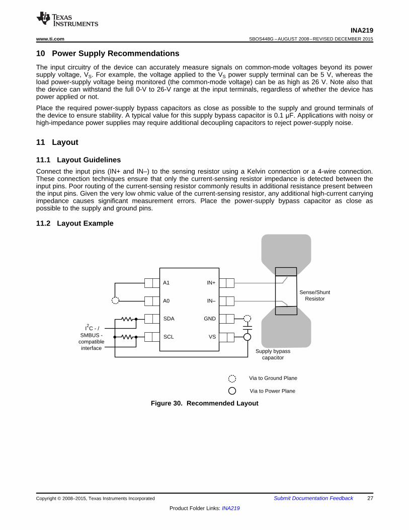
11 Layout
11.1 Layout GuidelinesConnect the input pins (IN+ and IN–) to the sensing resistor using a Kelvin connection or a 4-wire connection.These connection techniques ensure that only the current-sensing resistor impedance is detected between theinput pins. Poor routing of the current-sensing resistor commonly results in additional resistance present betweenthe input pins. Given the very low ohmic value of the current-sensing resistor, any additional high-current carryingimpedance causes significant measurement errors. Place the power-supply bypass capacitor as close aspossible to the supply and ground pins.
11.2 Layout Example
Figure 30. Recommended Layout
Copyright © 2008–2015, Texas Instruments Incorporated Submit Documentation Feedback 27
Product Folder Links: INA219
INA219SBOS448G –AUGUST 2008–REVISED DECEMBER 2015 www.ti.com
12 Device and Documentation Support
12.1 Community ResourcesThe following links connect to TI community resources. Linked contents are provided "AS IS" by the respectivecontributors. They do not constitute TI specifications and do not necessarily reflect TI's views; see TI's Terms ofUse.
TI E2E™ Online Community TI's Engineer-to-Engineer (E2E) Community. Created to foster collaborationamong engineers. At e2e.ti.com, you can ask questions, share knowledge, explore ideas and helpsolve problems with fellow engineers.
Design Support TI's Design Support Quickly find helpful E2E forums along with design support tools andcontact information for technical support.
12.2 TrademarksE2E is a trademark of Texas Instruments.All other trademarks are the property of their respective owners.
12.3 Electrostatic Discharge CautionThese devices have limited built-in ESD protection. The leads should be shorted together or the device placed in conductive foamduring storage or handling to prevent electrostatic damage to the MOS gates.
12.4 GlossarySLYZ022 — TI Glossary.
This glossary lists and explains terms, acronyms, and definitions.
13 Mechanical, Packaging, and Orderable InformationThe following pages include mechanical, packaging, and orderable information. This information is the mostcurrent data available for the designated devices. This data is subject to change without notice and revision ofthis document. For browser-based versions of this data sheet, refer to the left-hand navigation.
28 Submit Documentation Feedback Copyright © 2008–2015, Texas Instruments Incorporated
Product Folder Links: INA219
PACKAGE OPTION ADDENDUM
www.ti.com 29-Aug-2017
Addendum-Page 1
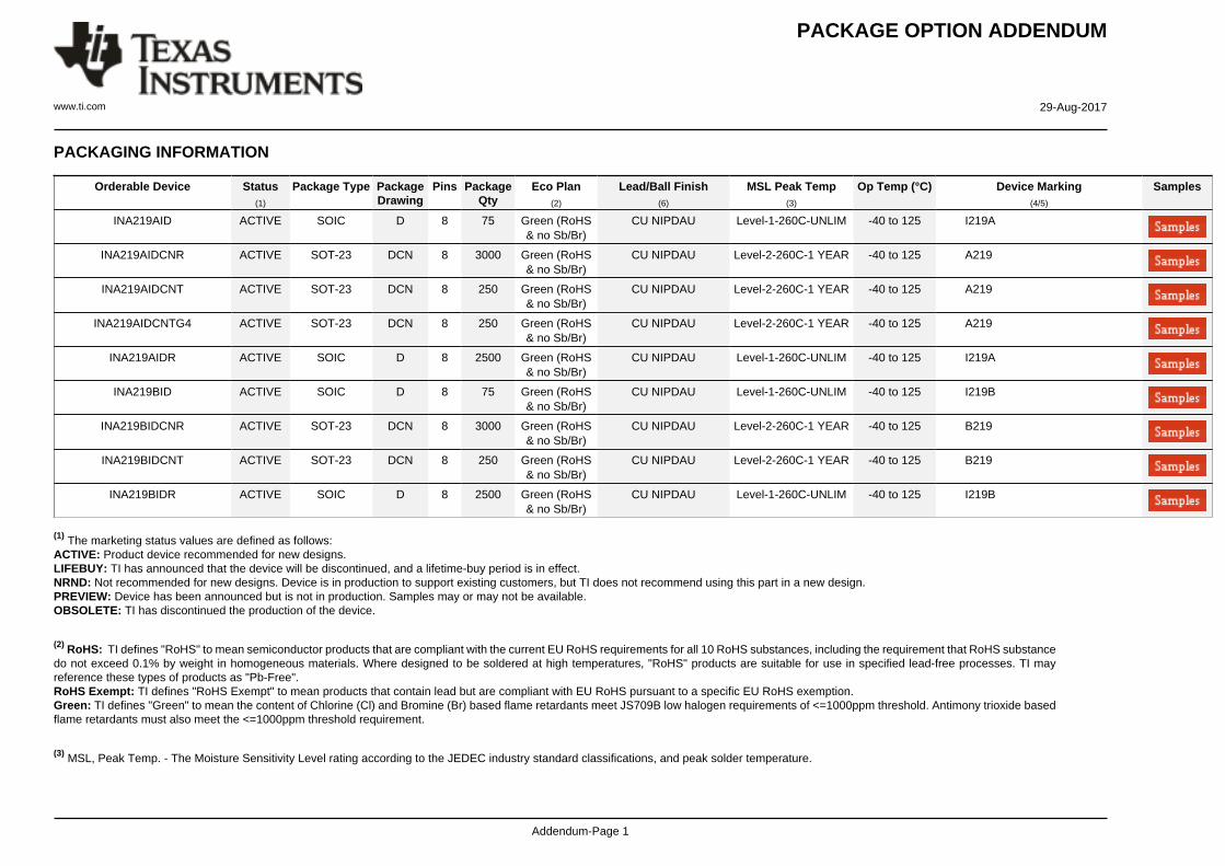
PACKAGING INFORMATION
Orderable Device Status(1)
Package Type PackageDrawing
Pins PackageQty
Eco Plan(2)
Lead/Ball Finish(6)
MSL Peak Temp(3)
Op Temp (°C) Device Marking(4/5)
Samples
INA219AID ACTIVE SOIC D 8 75 Green (RoHS& no Sb/Br)
CU NIPDAU Level-1-260C-UNLIM -40 to 125 I219A
INA219AIDCNR ACTIVE SOT-23 DCN 8 3000 Green (RoHS& no Sb/Br)
CU NIPDAU Level-2-260C-1 YEAR -40 to 125 A219
INA219AIDCNT ACTIVE SOT-23 DCN 8 250 Green (RoHS& no Sb/Br)
CU NIPDAU Level-2-260C-1 YEAR -40 to 125 A219
INA219AIDCNTG4 ACTIVE SOT-23 DCN 8 250 Green (RoHS& no Sb/Br)
CU NIPDAU Level-2-260C-1 YEAR -40 to 125 A219
INA219AIDR ACTIVE SOIC D 8 2500 Green (RoHS& no Sb/Br)
CU NIPDAU Level-1-260C-UNLIM -40 to 125 I219A
INA219BID ACTIVE SOIC D 8 75 Green (RoHS& no Sb/Br)
CU NIPDAU Level-1-260C-UNLIM -40 to 125 I219B
INA219BIDCNR ACTIVE SOT-23 DCN 8 3000 Green (RoHS& no Sb/Br)
CU NIPDAU Level-2-260C-1 YEAR -40 to 125 B219
INA219BIDCNT ACTIVE SOT-23 DCN 8 250 Green (RoHS& no Sb/Br)
CU NIPDAU Level-2-260C-1 YEAR -40 to 125 B219
INA219BIDR ACTIVE SOIC D 8 2500 Green (RoHS& no Sb/Br)
CU NIPDAU Level-1-260C-UNLIM -40 to 125 I219B
(1) The marketing status values are defined as follows:ACTIVE: Product device recommended for new designs.LIFEBUY: TI has announced that the device will be discontinued, and a lifetime-buy period is in effect.NRND: Not recommended for new designs. Device is in production to support existing customers, but TI does not recommend using this part in a new design.PREVIEW: Device has been announced but is not in production. Samples may or may not be available.OBSOLETE: TI has discontinued the production of the device.
(2) RoHS: TI defines "RoHS" to mean semiconductor products that are compliant with the current EU RoHS requirements for all 10 RoHS substances, including the requirement that RoHS substancedo not exceed 0.1% by weight in homogeneous materials. Where designed to be soldered at high temperatures, "RoHS" products are suitable for use in specified lead-free processes. TI mayreference these types of products as "Pb-Free".RoHS Exempt: TI defines "RoHS Exempt" to mean products that contain lead but are compliant with EU RoHS pursuant to a specific EU RoHS exemption.Green: TI defines "Green" to mean the content of Chlorine (Cl) and Bromine (Br) based flame retardants meet JS709B low halogen requirements of <=1000ppm threshold. Antimony trioxide basedflame retardants must also meet the <=1000ppm threshold requirement.
(3) MSL, Peak Temp. - The Moisture Sensitivity Level rating according to the JEDEC industry standard classifications, and peak solder temperature.
PACKAGE OPTION ADDENDUM
www.ti.com 29-Aug-2017
Addendum-Page 2
(4) There may be additional marking, which relates to the logo, the lot trace code information, or the environmental category on the device.
(5) Multiple Device Markings will be inside parentheses. Only one Device Marking contained in parentheses and separated by a "~" will appear on a device. If a line is indented then it is a continuationof the previous line and the two combined represent the entire Device Marking for that device.
(6) Lead/Ball Finish - Orderable Devices may have multiple material finish options. Finish options are separated by a vertical ruled line. Lead/Ball Finish values may wrap to two lines if the finishvalue exceeds the maximum column width.
Important Information and Disclaimer:The information provided on this page represents TI's knowledge and belief as of the date that it is provided. TI bases its knowledge and belief on informationprovided by third parties, and makes no representation or warranty as to the accuracy of such information. Efforts are underway to better integrate information from third parties. TI has taken andcontinues to take reasonable steps to provide representative and accurate information but may not have conducted destructive testing or chemical analysis on incoming materials and chemicals.TI and TI suppliers consider certain information to be proprietary, and thus CAS numbers and other limited information may not be available for release.
In no event shall TI's liability arising out of such information exceed the total purchase price of the TI part(s) at issue in this document sold by TI to Customer on an annual basis.
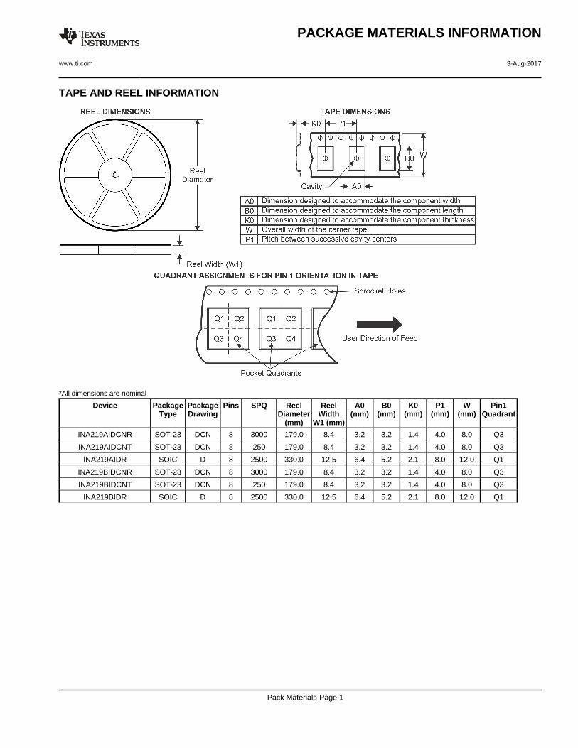
TAPE AND REEL INFORMATION
*All dimensions are nominal
Device PackageType
PackageDrawing
Pins SPQ ReelDiameter
(mm)
ReelWidth
W1 (mm)
A0(mm)
B0(mm)
K0(mm)
P1(mm)
W(mm)
Pin1Quadrant
INA219AIDCNR SOT-23 DCN 8 3000 179.0 8.4 3.2 3.2 1.4 4.0 8.0 Q3
INA219AIDCNT SOT-23 DCN 8 250 179.0 8.4 3.2 3.2 1.4 4.0 8.0 Q3
INA219AIDR SOIC D 8 2500 330.0 12.5 6.4 5.2 2.1 8.0 12.0 Q1
INA219BIDCNR SOT-23 DCN 8 3000 179.0 8.4 3.2 3.2 1.4 4.0 8.0 Q3
INA219BIDCNT SOT-23 DCN 8 250 179.0 8.4 3.2 3.2 1.4 4.0 8.0 Q3
INA219BIDR SOIC D 8 2500 330.0 12.5 6.4 5.2 2.1 8.0 12.0 Q1
PACKAGE MATERIALS INFORMATION
www.ti.com 3-Aug-2017
Pack Materials-Page 1
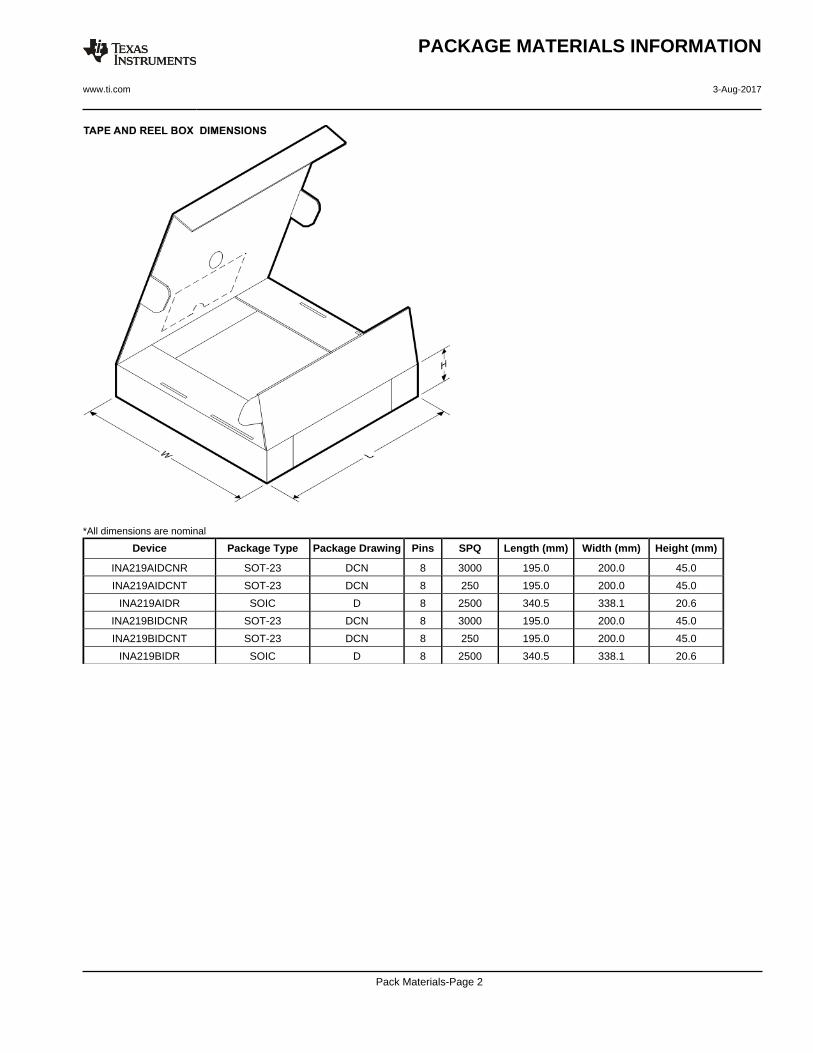
*All dimensions are nominal
Device Package Type Package Drawing Pins SPQ Length (mm) Width (mm) Height (mm)
INA219AIDCNR SOT-23 DCN 8 3000 195.0 200.0 45.0
INA219AIDCNT SOT-23 DCN 8 250 195.0 200.0 45.0
INA219AIDR SOIC D 8 2500 340.5 338.1 20.6
INA219BIDCNR SOT-23 DCN 8 3000 195.0 200.0 45.0
INA219BIDCNT SOT-23 DCN 8 250 195.0 200.0 45.0
INA219BIDR SOIC D 8 2500 340.5 338.1 20.6
PACKAGE MATERIALS INFORMATION
www.ti.com 3-Aug-2017
Pack Materials-Page 2


IMPORTANT NOTICE
Texas Instruments Incorporated (TI) reserves the right to make corrections, enhancements, improvements and other changes to itssemiconductor products and services per JESD46, latest issue, and to discontinue any product or service per JESD48, latest issue. Buyersshould obtain the latest relevant information before placing orders and should verify that such information is current and complete.TI’s published terms of sale for semiconductor products (http://www.ti.com/sc/docs/stdterms.htm) apply to the sale of packaged integratedcircuit products that TI has qualified and released to market. Additional terms may apply to the use or sale of other types of TI products andservices.Reproduction of significant portions of TI information in TI data sheets is permissible only if reproduction is without alteration and isaccompanied by all associated warranties, conditions, limitations, and notices. TI is not responsible or liable for such reproduceddocumentation. Information of third parties may be subject to additional restrictions. Resale of TI products or services with statementsdifferent from or beyond the parameters stated by TI for that product or service voids all express and any implied warranties for theassociated TI product or service and is an unfair and deceptive business practice. TI is not responsible or liable for any such statements.Buyers and others who are developing systems that incorporate TI products (collectively, “Designers”) understand and agree that Designersremain responsible for using their independent analysis, evaluation and judgment in designing their applications and that Designers havefull and exclusive responsibility to assure the safety of Designers' applications and compliance of their applications (and of all TI productsused in or for Designers’ applications) with all applicable regulations, laws and other applicable requirements. Designer represents that, withrespect to their applications, Designer has all the necessary expertise to create and implement safeguards that (1) anticipate dangerousconsequences of failures, (2) monitor failures and their consequences, and (3) lessen the likelihood of failures that might cause harm andtake appropriate actions. Designer agrees that prior to using or distributing any applications that include TI products, Designer willthoroughly test such applications and the functionality of such TI products as used in such applications.TI’s provision of technical, application or other design advice, quality characterization, reliability data or other services or information,including, but not limited to, reference designs and materials relating to evaluation modules, (collectively, “TI Resources”) are intended toassist designers who are developing applications that incorporate TI products; by downloading, accessing or using TI Resources in anyway, Designer (individually or, if Designer is acting on behalf of a company, Designer’s company) agrees to use any particular TI Resourcesolely for this purpose and subject to the terms of this Notice.TI’s provision of TI Resources does not expand or otherwise alter TI’s applicable published warranties or warranty disclaimers for TIproducts, and no additional obligations or liabilities arise from TI providing such TI Resources. TI reserves the right to make corrections,enhancements, improvements and other changes to its TI Resources. TI has not conducted any testing other than that specificallydescribed in the published documentation for a particular TI Resource.Designer is authorized to use, copy and modify any individual TI Resource only in connection with the development of applications thatinclude the TI product(s) identified in such TI Resource. NO OTHER LICENSE, EXPRESS OR IMPLIED, BY ESTOPPEL OR OTHERWISETO ANY OTHER TI INTELLECTUAL PROPERTY RIGHT, AND NO LICENSE TO ANY TECHNOLOGY OR INTELLECTUAL PROPERTYRIGHT OF TI OR ANY THIRD PARTY IS GRANTED HEREIN, including but not limited to any patent right, copyright, mask work right, orother intellectual property right relating to any combination, machine, or process in which TI products or services are used. Informationregarding or referencing third-party products or services does not constitute a license to use such products or services, or a warranty orendorsement thereof. Use of TI Resources may require a license from a third party under the patents or other intellectual property of thethird party, or a license from TI under the patents or other intellectual property of TI.TI RESOURCES ARE PROVIDED “AS IS” AND WITH ALL FAULTS. TI DISCLAIMS ALL OTHER WARRANTIES ORREPRESENTATIONS, EXPRESS OR IMPLIED, REGARDING RESOURCES OR USE THEREOF, INCLUDING BUT NOT LIMITED TOACCURACY OR COMPLETENESS, TITLE, ANY EPIDEMIC FAILURE WARRANTY AND ANY IMPLIED WARRANTIES OFMERCHANTABILITY, FITNESS FOR A PARTICULAR PURPOSE, AND NON-INFRINGEMENT OF ANY THIRD PARTY INTELLECTUALPROPERTY RIGHTS. TI SHALL NOT BE LIABLE FOR AND SHALL NOT DEFEND OR INDEMNIFY DESIGNER AGAINST ANY CLAIM,INCLUDING BUT NOT LIMITED TO ANY INFRINGEMENT CLAIM THAT RELATES TO OR IS BASED ON ANY COMBINATION OFPRODUCTS EVEN IF DESCRIBED IN TI RESOURCES OR OTHERWISE. IN NO EVENT SHALL TI BE LIABLE FOR ANY ACTUAL,DIRECT, SPECIAL, COLLATERAL, INDIRECT, PUNITIVE, INCIDENTAL, CONSEQUENTIAL OR EXEMPLARY DAMAGES INCONNECTION WITH OR ARISING OUT OF TI RESOURCES OR USE THEREOF, AND REGARDLESS OF WHETHER TI HAS BEENADVISED OF THE POSSIBILITY OF SUCH DAMAGES.Unless TI has explicitly designated an individual product as meeting the requirements of a particular industry standard (e.g., ISO/TS 16949and ISO 26262), TI is not responsible for any failure to meet such industry standard requirements.Where TI specifically promotes products as facilitating functional safety or as compliant with industry functional safety standards, suchproducts are intended to help enable customers to design and create their own applications that meet applicable functional safety standardsand requirements. Using products in an application does not by itself establish any safety features in the application. Designers mustensure compliance with safety-related requirements and standards applicable to their applications. Designer may not use any TI products inlife-critical medical equipment unless authorized officers of the parties have executed a special contract specifically governing such use.Life-critical medical equipment is medical equipment where failure of such equipment would cause serious bodily injury or death (e.g., lifesupport, pacemakers, defibrillators, heart pumps, neurostimulators, and implantables). Such equipment includes, without limitation, allmedical devices identified by the U.S. Food and Drug Administration as Class III devices and equivalent classifications outside the U.S.TI may expressly designate certain products as completing a particular qualification (e.g., Q100, Military Grade, or Enhanced Product).Designers agree that it has the necessary expertise to select the product with the appropriate qualification designation for their applicationsand that proper product selection is at Designers’ own risk. Designers are solely responsible for compliance with all legal and regulatoryrequirements in connection with such selection.Designer will fully indemnify TI and its representatives against any damages, costs, losses, and/or liabilities arising out of Designer’s non-compliance with the terms and provisions of this Notice.
Mailing Address: Texas Instruments, Post Office Box 655303, Dallas, Texas 75265Copyright © 2017, Texas Instruments Incorporated


![Atmel SAM D10 - Farnell element14 · SAM D10D – 24-pin QFN SAM D10D – 20-pin SOIC SAM D10C – 14-pin SOIC. Atmel | SMART SAM D10 [PRELIMINARY DATASHEET SUMMARY] 5 Atmel-42242BS-SAM-D10-Summary_07/2015](https://img.pdfslide.net/doc/110x75/5f843fea40614d2e5d2c3ec2/atmel-sam-d10-farnell-sam-d10d-a-24-pin-qfn-sam-d10d-a-20-pin-soic-sam-d10c.jpg)