Embed Size (px)
Citation preview

1
Inclusion of Switching Loss in theAveraged Equivalent Circuit Model
The methods of Chapter 3 can be extended to include switching loss inthe converter equivalent circuit model
• Include switching transitions in the converter waveforms
• Model effects of diode reverse recovery, etc.
To obtain tractable results, the waveforms during the switchingtransitions must usually be approximated
Things that can substantially change the results:
• Ringing caused by parasitic tank circuits
• Snubber circuits
• These are modeled in ECEN 5817, Resonant and Soft-Switching Phenomena in Power Electronics

2
The Modeling ApproachExtension of Chapter 3 Methods
Sketch the converter waveforms– Including the switching transitions (idealizing assumptions
are made to lead to tractable results)
– In particular, sketch inductor voltage, capacitor current, andinput current waveforms
The usual steady-state relationships: vL = 0, iC = 0, ig = Ig
Use the resulting equations to construct an equivalentcircuit model, as usual

3
Buck Converter Example
• Ideal MOSFET, p–n diode with reverse recovery• Neglect semiconductor device capacitances, MOSFET
switching times, etc.• Neglect conduction losses• Neglect ripple in inductor current and capacitor voltage

4
Assumedwaveforms
Diode recovered charge Qr,
reverse recovery time tr
These waveforms assumethat the diode voltagechanges at the end of thereverse recovery transient
• a “snappy” diode
• Voltage of soft-recoverydiodes changes sooner
• Leads to a pessimisticestimate of inducedswitching loss

5
Inductor volt-second balanceand capacitor charge balance
As usual: vL = 0 = DVg – V
Also as usual: iC = 0 = IL – V/R

6
Average input current
ig = Ig = (area under curve)/Ts
= (DTsIL + trIL + Qr)/Ts
= DIL + trIL /Ts + Qr /Ts
7
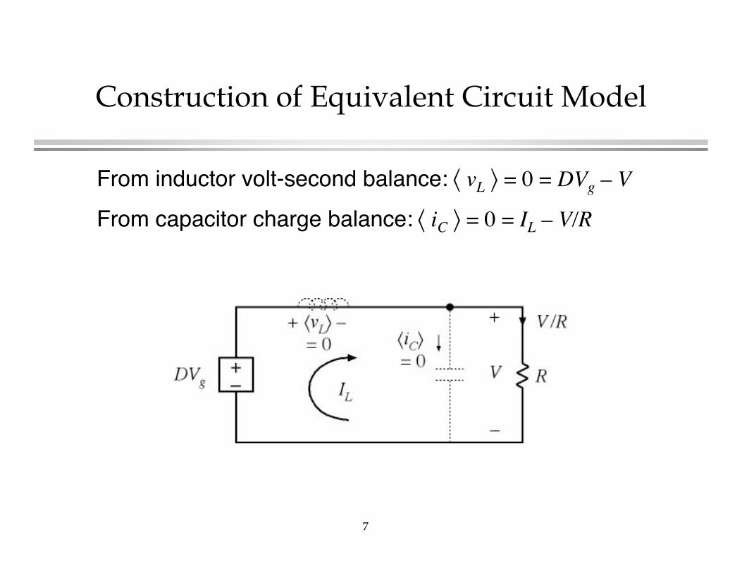
Construction of Equivalent Circuit Model
From inductor volt-second balance: vL = 0 = DVg – V
From capacitor charge balance: iC = 0 = IL – V/R

8
Input port of model
ig = Ig = DIL + trIL /Ts + Qr /Ts

9
Combine for complete model
The two independent current sources consume power
Vg (trIL /Ts + Qr /Ts)
equal to the switching loss induced by diode reverse recovery

10
Solution of model
Output:
V = DVg
Efficiency: = Pout / Pin
Pout = VIL Pin = Vg (DIL + trIL /Ts + Qr /Ts)
Combine and simplify:
= 1 / [1 + fs (tr /D + Qr R /D2Vg )]
11
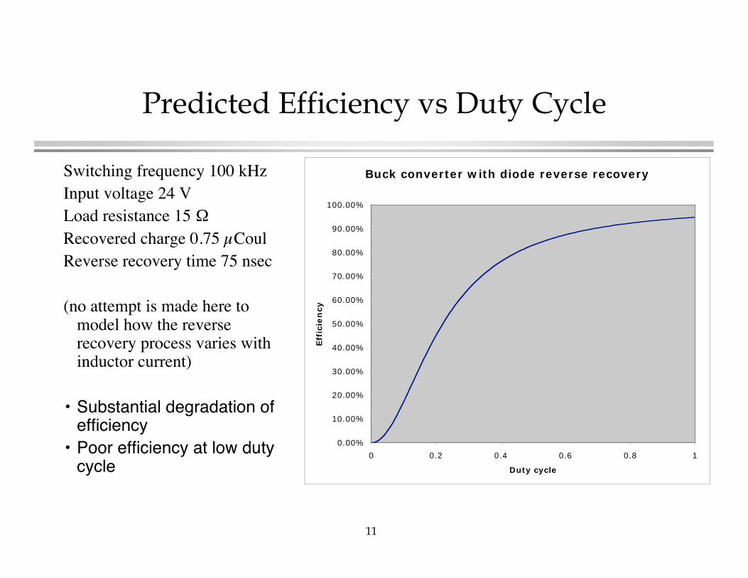
Predicted Efficiency vs Duty Cycle
Switching frequency 100 kHzInput voltage 24 VLoad resistance 15 Recovered charge 0.75 µCoulReverse recovery time 75 nsec
(no attempt is made here tomodel how the reverserecovery process varies withinductor current)
• Substantial degradation ofefficiency
• Poor efficiency at low dutycycle
Buck converter with diode reverse recovery
0.00%
10.00%
20.00%
30.00%
40.00%
50.00%
60.00%
70.00%
80.00%
90.00%
100.00%
0 0.2 0.4 0.6 0.8 1
Duty cycle
Eff
icie
ncy

12
Boost Converter Example
Model same effects as in previous buck converter example:• Ideal MOSFET, p–n diode with reverse recovery• Neglect semiconductor device capacitances, MOSFET
switching times, etc.• Neglect conduction losses• Neglect ripple in inductor current and capacitor voltage

13
Boostconverter
Transistor and diodewaveforms have sameshapes as in buckexample, but dependon different quantities

14
Inductor volt-second balanceand average input current
As usual: vL = 0 = Vg – D V
Also as usual: ig = IL

15
Capacitorcharge balance
iC = id – V/R = 0
= – V/R + IL(D Ts – tr)/Ts – Qr /Ts
Collect terms: V/R = IL(D Ts – tr)/Ts – Qr /Ts

16
Construct model
The two independent current sources consume power
V (trIL /Ts + Qr /Ts)
equal to the switching loss induced by diode reverse recovery
The result is:

17
Predicted V/Vg vs duty cycle
Boost converter with diode reverse recovery
0
1
2
3
4
5
6
7
8
0 0.2 0.4 0.6 0.8 1
Duty cycle
V/
Vg
Switching frequency 100 kHzInput voltage 24 VLoad resistance 60 Recovered charge 5 µCoulReverse recovery time 100 nsecInductor resistance RL = 0.3 (inductor resistance also inserted
into averaged model here)
With RL only
With RL and diode reverse recovery

18
Summary
The averaged modeling approach can be extended toinclude effects of switching loss
Transistor and diode waveforms are constructed,including the switching transitions. The effects of theswitching transitions on the inductor, capacitor, andinput current waveforms can then be determined
Inductor volt-second balance and capacitor chargebalance are applied
Converter input current is averagedEquivalent circuit corresponding to the the averaged
equations is constructed