Embed Size (px)
Citation preview

INDIUM PHOSPHIDE FOR HIGH FREQUENCY
POWER TRANSISTORS
V. L. Wrick, W. J. Choyke,and R. C. Clarke
Final ReportFor Period 22 March 1979to 28 April 1980
September 1980
Sponsored by:
Defense Advanced Research Projects Agency (DOD)DARPA Order No. 3535Monitored by Office of Naval ResearchDept. of Navy, Arlington, VA 22217 underContract No. N00014-78-C-0254
Approved for public release; distribution unlimited.
The views and conclusions contained in this document arethose of the authors and should not be interpreted asnecesarily representing the official policies, eitherexpressed or implied, of the Defense Advanced ResearchProjects Agency or the U. S. Government.
0Westinghouse R&D Center
1310 Beulah RoadPittsburgh. Pennsylvania 15235
_____ ____ ____* ~ .h..........I

4
Processing technology concentrated on a self-aligned diffused gateJFET structure. This technique produced working microwave transistors(JFET) up to 1200 wm in gate periphery. The report compares these devicesto similar GaAs transistors (MESFET) and makes recommendations for futurestudies.
BT-- bu to l.
jhfr.-I0- -
3 i tif rt. *~
I del
~\~_Lc-d

TABLE OF CONTENTS
Page
LIST OF ILLUSTRATIONS ......... ................... ii
LIST OF TABLES ......... ...................... iv
1. INTRODUCTION ........... ....................... 1
2. VAPOR PHASE EPITAXY .......... .................... 4
2.1 Introduction .......... ..................... 4
2.2 Growth Transients ......... .................. 4
2.3 Gas Phase Stoichiometry-V/III Ratio .... ......... 7
2.4 Buffer Layers .......... .................... 7
2.5 Sulfur Doping ........ .................... 10
2.6 Sulfur Doped Device Structures ... ............ . l.11
2.7 Summary ......... ....................... 11
3. ION IMPLANTATION ........ ..................... 17
3.1 Experimental Results ...... ................. . 18
4. DEVICES ........... .......................... 28
4.1 Diffused Junction Technology .... ............. .. 28
4.2 InP DJFET Fabrication and Performance .. ........ . 37
4.3 Comparison Between InP DJFET and GaAs MESFET ........ 46
5. CONCLUSIONS AND RECOMMENDATIONS FOR FURTHER STUDY ....... 52
6. REFERENCES .......... ........................ 54
7. ACKNOWLEDGEMENTS ........ ..................... 55
8. PRESENTATIONS AND PUBLICATIONS ..... .............. 56

LIST OF ILLUSTRATIONS
Figure Page
2.1 Doping vs. depth curve illustrating enhanced 6
impurity incorporation at epilayer substrate
interface.
2.2 Net impurity incorporation vs. gas phase 8
stoichiometry, III/V ratio.
2.3 The mole fraction of introduced PCZ 3 influences 9
the residual impurity incorporation.
2.4 Epitaxial layer thickness versus growth time 12
for mole fraction PCZ = 10 - 2.
2.5 Sulfur incorporation as electrically active 13
impurity as a function of H2 S pressure in the
reactor.
2.6 The carrier concentration depth profile of an 14
FET structure on a semi-insulating buffer layer.
2.7 Etching of Hall specimens shows that the 15
surface channel mobility is retained throughout
the channel.
3.1 Schematic representation of "masked" InP sample 20
during implantation.
3.2 Rutherford backscatter data for sample JCl on both 21
implanted and unimplanted halves.
3.3 Rutherford backscatter data for sample A before 23
anneal.
3.4 Rutherford backscatter data for sample D, before 24
anneal.
3.5 Rutherford backscatter data for sample A after 25
anneal at 400 0 C for 24 hr.
3.6 Rutherford backscatter data for sample D after 26
anneal at 400*C for 24 hr.
ii'
LIST OF ILLUSTRATIONS (Continued)
Figure Page
4.1 "Unassisted" AZ Schottky barrier I-V 29characteristic on 1017 n-type InP.
4.2 Self aligned diffused p-n junctions on InP. 30
4.3 I-V characteristic of DVIll-U (5 mil test dot). 32
4.4 I-V characteristic of DVI11-2 (5 mil diameter 33test dot).
4.5 I-V characteristic of DVI11-3 (5 mil diameter 34test dot).
4.6 I/C2 vs. V for Zn-Ak diode alloyed at 2001C for 3519 hr (sample DVllI-3).
4.7 Auger measurements of AZ and Zn diffusion 36concentration as a function of distance forsamples held at 200 0C for 4.5 and 19 hr.
4.8 Realigned InP FET fabrication sequence using 38
oxide assisted gate.
4.9 Realigned InP DJFET fabrication. 39
4.10 DC InP DJFET I-V characteristics. 41
4.11 Microwave scattering parameters for 300 p InP 42DJFET measured from 2 to 12 GHz.
4.12 Broadband model of 300 P InP DJFET. Values in 43parentheses are representative of a similar GaAsMESFET.
4.13 InP DJFET (1200 p periphery) tuned for power 45
at 17 dbm.
4.14 Gain vs. frequency comparison for microwave FET's. 48
4.15 Feedback capacitance vs. gate bias w. drain bias 49fixed for InP DJFET (300 p).
4.16 Feedback capacitance vs. gate bias w. drain bias 50fixed for GaAs MESFET (900 p).
ill
LIST OF TABLES
Table Page
1.1 Technological Problems with the InP FET 3
1.2 Theoretical Questions Regarding the Viability 3of the InP Power FET
2.1 The Electrical Properties of Undoped Indium 10Phosphide Epitaxial Layers
3.1 Review of Amorphization of Implant Conditions 19
4.1 Anneal Conditions for AZ-Zn Diffused 37Junction Test Structures
iv

1. INTRODUCTION
The objective of this program has been to determine
the utility of InP for producing power microwave field effect transis-
tors (FET's). InP was originally considered as an alternative to GaAs
because of several material parameters which theoretically offered
improved device performance. Table 1-1 lists the key parameters and
how one would expect them to impact FET operation. InP has been inves-
tigated in the past; hence,some of its drawbacks are also documented.
Table 1-2 reviews the technological and theoretical problems associated
with InP power FET's. The previous interim report reviewed the progress
in achieving the technological goals of the program.
This report discusses the concluding effort which filled in the gaps in
the lnP FET technology base. The resulting transistors were extensively
tested and modeled in an attempt to address the larger theoretical
question of InP's place as an FET material.
The major technological problem with InP has been the low
Schottky barrier height of metals on n-type InP. The previous report
has detailed the Westinghouse studies on dielectric enhanced barriers.
In light of these studies, it was determined that a p-n junction should
provide the most reliable gating technique on InP. In the long term,
ion implantation was deemed the best approach to achieving shallow,
degenerate p-type doping for 1 ijm gate lengths. Ion implantation, how-
ever, requires further development to consistently deliver these results.
Therefore, preliminary work was begun on improving the p-type implant
technology base, and simultaneously, a self-aligned diffused junction
transistor was fabricated. This "demonstration vehicle" was then
microwave tested and modeled to allow the opportunity for an analysis
of device behavior.
|1

This report represents the conclusion of the effort to inves-
tigate power InP FET's. Over the course of the program, reliable InP
vapor phase epitaxy (VPE) and ion implantation were developed to support
the device investigation. Amorphization and low temperature recrystal-
lization of 3 1p implants in InP were observed. A broad spectrum of
gate technologies were addressed and a reasonable demonstration tech-
nique was achieved. Finally, rf modeling of the devices allowed a semi-
quantitative comparison between the InP JFET and its counterpart, the
GaAs MESFET. Recommendations for further study are included in the
final section of the report.
2

Table 1-1
Technological Problems with the InP FET
A. Reproducible, High Mobility VPE Layers Suitable
for FET Fabrication
B. Develop Low Leakage Schottky Gate
C. Develop P-N Junction Gate
a. Ion Implantation
h. Diffused Junction
Table 1-2
Theoretical Questions Regarding theViability of the InP Power FET
A. Determine the Nature and Behavior of the
Gate-Drain Feedback Capacitance
B. Determine Device Design Parameters (Gate Length,
Gate-Drain Spacing, Doping, Gate Recess) Which
Differ from GaAs Technology in Affecting the
Power and Frequency Limitations of the Device
3

2. VAPOR PHASE EPITAXY
2.1 Introduction
The PCZ 3 jInIH 2 or chloride process for the growth of indium
phosphide epitaxial layers has been in use for many years. A carefully
controlled concentration of phosphorus trichloride vapor in hydrogen is
passed over indium at high tempera, res (700-750'C) and the products,
indium monochloride and phosphorus vapor, pass over polished seed wafers
at 650 0 C. Epitaxy of indium phosphide subsequently takes place on the
seed wafer with a growth rate and impurity content dependent on the
purity of the raw materials and, more importantly, on the growth condi-
tions employed. The mole fraction of phosphorus trichloride, the gas
phase stoichiometry, and the source and seed temperature distribution
profiles are the most significant variables in the process.
For electronic devices a thin layer of semiconductor is grown
on the surface of an indium phosphide seed wafer and, as the layer pro-
pagates away from the substrate, impurities are deliberately added to
modify the crystal so as to produce a controlled profile of electron
concentration with depth, frequently with submicron dimensions. Our
previous report (243-023-Tl, Annual Technical Report, September 1979)
discussed the reactor design for epitaxy of InP, morphology control,
multilayer growth and wafer characterization. At that time, however,
a problem with the appearance of a low mobility conducting region at
the interface between the iron doped substrates and the buffer layers
occurred. This layer has now been eliminated.
2.2 Growth Transients
The interface layer was traced to the growth transients during
the heating of the epitaxial system. Since all the indium phosphide
4

that dissolved in the indium melt has precipitated during cool-down,
in reheating the melt the solid must dissolve again. Using a furnace
with a heat pipe to promote an even temperature over the source, and
using an initial heating cycle designed to prevent seed decomposition,
the epitaxial deposition can begin with the passage of PCZ 3 vapor over
the source. However, a transient occurs at the moment of the arrival
of the PCZ 3 at the source. Phosphorus formed by the decomposition of
PCZ 3 in hydrogen dissolves in the exposed indium melt to cover the
same with a skin of indium phosphide. The length of the transient is a
function of the rate of arrival of phosphorus vapor and the source
dimensions and temperature gradient. This phenomenon is significant
because it embodies a changing gas phase stoichiometry over the seeds.
At first the phosphorus pressure over the seeds is determined by the
indium phosphide decomposition at the source but as the skin area be-
comes a greater fraction of the total, phosphorus begins to flow past
the source. Thus, we can expect a gradually increasing phosphorus to
indium ratio until the steady state is reached. Ten to fifteen minutes
pre-growth saturation times for 100g sources are frequently observed,
and these increase proportionately with source dimensions. Even if the
phosphorus trichloride flow is stopped during growth and then restarted,
the pregrowth saturation recurs and creates a rapidly changing gas
phase stoichiometry. The significance of this for the controlled growth
of multilayers is that the incorporation of indigenous dopants is a
strong function of the gas phase stoichiometry and consequently, rapid
swings in carrier concentration have been observed in association with
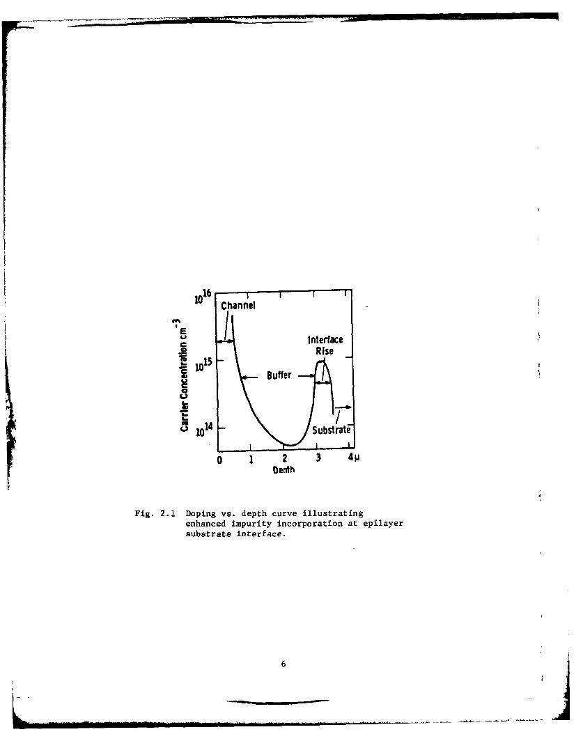
source saturation.1 A typical substrate-buffer interface peak for a
system using a 250 g indium melt is shown in Fig. 2.1. The material
grown during the uncontrolled gas phase stoichiometry demonstrates low
Hall mobility (-1000 cm2/V-s), suggesting a high degree of compensation.
We believe the interface problem is caused by an increase in the incor-
poration rate for silicon and other impurities by several orders of mag-
nitude during the changing gas phase stoichiometry associated with the
source saturation sequence.
5
io6Channel
Ec Interface
Rise
~ 1015Buffer
114 Su10 Substrate"
0 1 2 3 4Denth
Fig. 2.1 Doping vs. depth curve illustratingenhanced impurity incorporation at epilayersubstrate interface.
____ j
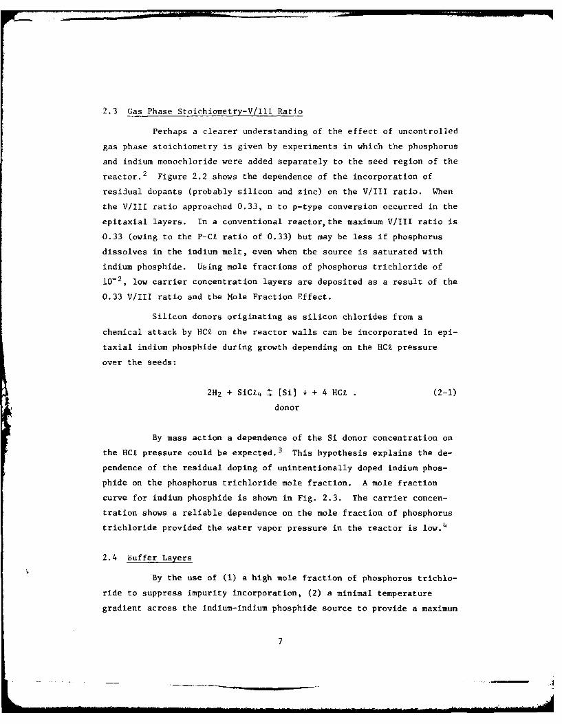
2.3 Gas Phase Stoichiometry-V/III Ratio
Perhaps a clearer understanding of the effect of uncontrolled
gas phase stoichiometry is given by experiments in which the phosphorus
and indium monochloride were added separately to the seed region of the
reactor.2 Figure 2.2 shows the dependence of the incorporation of
residual dopants (probably silicon and zinc) on the V/Ill ratio. When
the V/Ill ratio approached 0.33, n to p-type conversion occurred in the
epitaxial layers. In a conventional reactor, the maximum V/Ill ratio is
0.33 (owing to the P-CX ratio of 0.33) but may be less if phosphorus
dissolves in the indium melt, even when the source is saturated with
indium phosphide. Using mole fractions of phosphorus trichloride of
10-2, low carrier concentration layers are deposited as a result of the
0.33 V/Ill ratio and the Mole Fraction Effect.
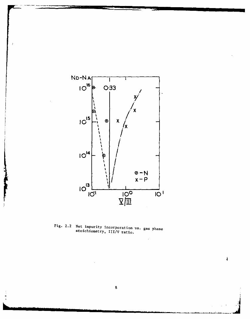
Silicon donors originating as silicon chlorides from a
chemical attack by HCZ on the reactor walls can be incorporated in epi-
taxial indium phosphide during growth depending on the HCZ pressure
over the seeds:
2H2 + SiCL4 ' [Si] + + 4 HCU . (2-1)
donor
By mass action a dependence of the Si donor concentration on
the HCZ pressure could be expected. 3 This hypothesis explains the de-
pendence of the residual doping of unintentionally doped indium phos-
phide on the phosphorus trichloride mole fraction. A mole fraction
curve for indium phosphide is shown in Fig. 2.3. The carrier concen-
tration shows a reliable dependence on the mole fraction of phosphorus
trichloride provided the water vapor pressure in the reactor is low. 4
2.4 buffer Layers
By the use of (1) a high mole fraction of phosphorus trichlo-
ride to suppress impurity incorporation, (2) a minimal temperature
gradient across the indium-indium phosphide source to provide a maximum
7
ND-NA
1016 &- 0.33
/X
101 /'6 /
IC , l
,to' -omtr, II/Vrto.... 'l
z I1 I"
10"1 I00 10'
Fig. 2.2 Net impurity incorporation vs. gas phasestoichiometry, III/V ratio.
8
L4
Curve 722800-A
10~0
10 3 0 4 10 15 10o16 1017Carrier Concentration. cmr
Fig. 2.3 The mole fraction of introduced PCR,3 influencesthe residual impurity incorporation.
9

V/II I r.it io and (3) the application of vaPor phase etching to avoid the
ettfet ts of source transients at the start of growth, [nP buffer layers
with low residual carrier concentration can be obtained. The results
of Van der Pauw analysis of a series of pure buffer layers is given in
Table 2.1.
Table 2.1
The Electrical Properties of Undoped Indium Phosphide Epitaxial Layers
The Van der Pauw Results of a Series of Epitaxial LayersGrown with Molar Fraction [PCZ 3] = 1.5 x 10⁻²
Run NO. ND-NA NDNA 1(300 K) (77 (300 K) (77 K)
88 4 x 10¹⁴ 3 x 10¹⁴ 4800 68000
89 4 x 101 5 1 x i01' 2340 17000
90 1.6 x 10¹⁴ 3 x 10¹⁴ 3600 51000
91 9 x 10¹⁴ 7 x 10¹⁴ 3400 40000
92 6 x 10¹⁴ 3 x 10¹⁴ 3000 53000
93 3 x 10¹⁴ 2.8 x 101 " 5200 90000
94 4 x 10¹⁴ 2.8 x 101 4 4700 86000
95 2 x 10¹⁴ 1.8 x I0 I' 5200 73000
96 2 x 10¹⁵ 2.1 x 10¹⁵ 3050 34000
97 2 c¢ 10 1 1 x i01"L 5300 71000
2.5 Sulfur Doping
Most electronic devices in n-type indium phosphide require an
internal structure which is usual'y fabricated by multilayered epitaxy.
For this purpose, an impurity with predictable incorporation character-
istics over a wide range of carrier concentration is added in a con-
trolled way to the undoped buffer layers. Sulfur, which shows
negligible dependence of incorporation on phosphorus trichloride mole
fraction, minimum dependence on V/Ill ratio and is only marginally
10

influenced by the reactor oxygen pressure, is easily obtained as a
dilute mixture of hydrogen sulfide in hydrogen. This dopant mixture is
electronically monitored and diluted with hydrogen before introduction
into the growth system and may be directed into the seed chamber by a
minimum dead space injection valve placed adjacent to the reaction tube
to reduce response time.
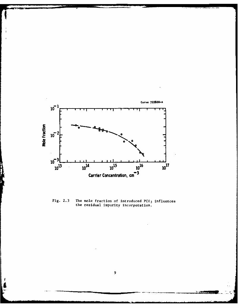
The growth rate of epitaxial buffer material against time is
shown in Fig. 2.4 and the steady state sulfur pressure in the reactor
against carrier concentration is shown in Fig. 2.5. Hence, knowing the
growth rate and doping efficiency, growth schedules for multilavered
epitaxy can be written. If the dopant injection circuits are small
bore so as to provide minimum response time, and the injection valves
and lines contain no dead space or unswept volume, it is possible to
achieve rising and falling interfaces between multilayers governed by
the diffusion of dopant in the semiconductor at growth temperature.
2.6 Sulfur Doped Device Structures
Figure 2.6 shows the buffer-channel interface of an FET
structure. The interface width at 1017 cm-3 is 500A, and the buffer
layer carrier concentration is less than 1013 cm- 3 . The buffer layer
grown on the iron doped substrate is highly resistive,showing greater
than 200V breakdown characteristics using tungsten probes. The channel
shows a 3800-3600 cm /V-s low field mobility at 1017 cm- 3 throughout
its depth, suggesting that the buffer layer has successfully prevented
electrical compensation by impurities from the iron doped substrate.
Figure 2.7 shows the MOS profile of the FET with the mobility profile
achieved by etching a Van der Pauw specimen from the same wafer.
2.7 Summary
The use of an indium liquid source with PCZ 3 vapor in hydrogen
to grow epitaxial InP has produced buffer (ND < 1013 cm- 3) and active
layers (ND 1017 cm-3 ) with high mobility and good morphology. The
11
Curve 717878-S
200
C
E 10
'S 5
Growth Time
Fig. 2.4 Epitaxial layer thickness versus growth time formole fraction PCZ3 =10-2.
12
E x10 17
EX 161
.01 .1 VmH2S LO0 10
Fig. 2.5 Sulfur incorporation as electrically activeimpurity as a function Of H2S pressure in thereactor.
13

17SixlO16
S1x101
L
154, lxlO15
1X IO 14 ' i I I I i I I I I I I
0.1 0.3 0.5 0.7 0.9 LI 3 L5P
Depth
Fig. 2.6 The carrier concentration depth profile
of an FET structure on a semi-insulatingbuffer layer.
14
Curve 717877-A
1xO 18 10000
L) ------ 70 Hall Data
170 XlO E
MOS Profile
16101IlO1 I. I I -L \ I I 1 100
0 0 .1 0.2 2a3 0.4 0.5 0.6 0.7 .8Depth. p
Fig. 2.7 Etching of Hall specimens shows that the
surface channel mobility is retained
throughout the channel.
I
15t
4r

initial problems with impurities at the buffer-substrate interface have
been eliminated. However, a system that fixed the V/Il ratio in the
vapor over the seed crystals would offer greater stability than the
present indium source method. This could well be a solid source system
using PCZ 3 as the transport gas which would be amenable to micropro-
cessor sequencing for the growth of controlled device layers.
16
3. ION IMPLANTATION
As discussed in the previous interim report, it was concluded
that a JFET would be the most suitable approach to sustain the voltages
and heat associated with InP power FET operation. Therefore, it was
decided that work on ion implantation should concentrate on p-type
dopants with the expectation that this would ultimately be the techno-
logy of choice for the JFET fabrication.
The InP junction gate FET (JFET) requires p-type implants
with (a) shallow, abrupt doping profiles typically 100OX deep, (b) p-
type doping in excess of the n-type active channel doping by at least a
factor of 10, and (c) resolution of 1 micron gate lengths if selective
implantation is used. P-type ion implantation in InP has been demon-
strated by Westinghouse but further work is clearly required to achieve
goals (a) and (b). One problem is low dopant activation, typically 20%.
Mg and Be implants have profiles which obey the LSS predictions. For
the high fluences which should satisfy condition (b), however, there
appears to be anomalous tail diffusion and a saturation of dopant
activition below the desired value.
Recent work by Tsai and Streemans has given rise to a new ion
implantation approach in Si (solid phase epitaxy) which has the dual
benefit of high activation and abrupt electrical profiles. The objec-
tive of our study was to try and exploit similar techniques in InP
p-type ion implantation. The underlying phenomena of the Tsai-Streetman
work was the solid phase epitaxy of amorphous Si. By amorphizing the
lattice with high dose Si implants, they provided a different host for
the boron doping implants. Where the boron profile overlapped the amor-
phous damage profile, solid phase epitaxy at low temperatures (550*C)
regrew the amorphized lattice and allowed almost complete activation,
i.e. proper site location of the boron in the crystal. This
17

effectively truncates the tail of the LSS profile, hence satisfying
both conditions (a) and (b) of our desired JFET implantation.
The same concepts should be applicable to compound semicon-
ductors ; however, there are certain problems that need to be overcome. Oxygen has
a notable effect on complexing species in both InP and GaAs, hence an
oxygen-free surface must be provided before the implant and maintained
through the solid regrowth step.
In addition, the implant and anneal conditions must be empi-
rically established which predictably amorphize the crystal and provide
true solid regrowth with dopant activation. The following section
reviews our experimental approach to satisfying these criteria.
3.1 Experimental Results
The first criterion to satisfy in the investigation was t
ability to successfully amorphize and recrystallize an InP sample. The
approach was to mask one half of an InP sample with At to
provide an "unimplanted" standard for comparison with the implanted
half. Figure 3.1 is a schematic representation of a sample during
implantation. Phorphorus was chosen as the "amorphizing" species
since it increases the vacancy level on the In sub-lattice and
hence aids the probable incorporation of Group II p-type dopants. Fol-
lowing the implant, the At was stripped from the InP using buffered HF.
Rutherford backscattering data was then collected on the samples to
determine the level of damage inflicted upon the InP with respect to
the unimplanted reference. Following the initial backscattering mea-
surements, annealing and another series of backscattering probes were
done to determine if the damage had been successfully removed. Table
3.1 lists the series of implants performed to understand the damage-
regrowth phenomenon.
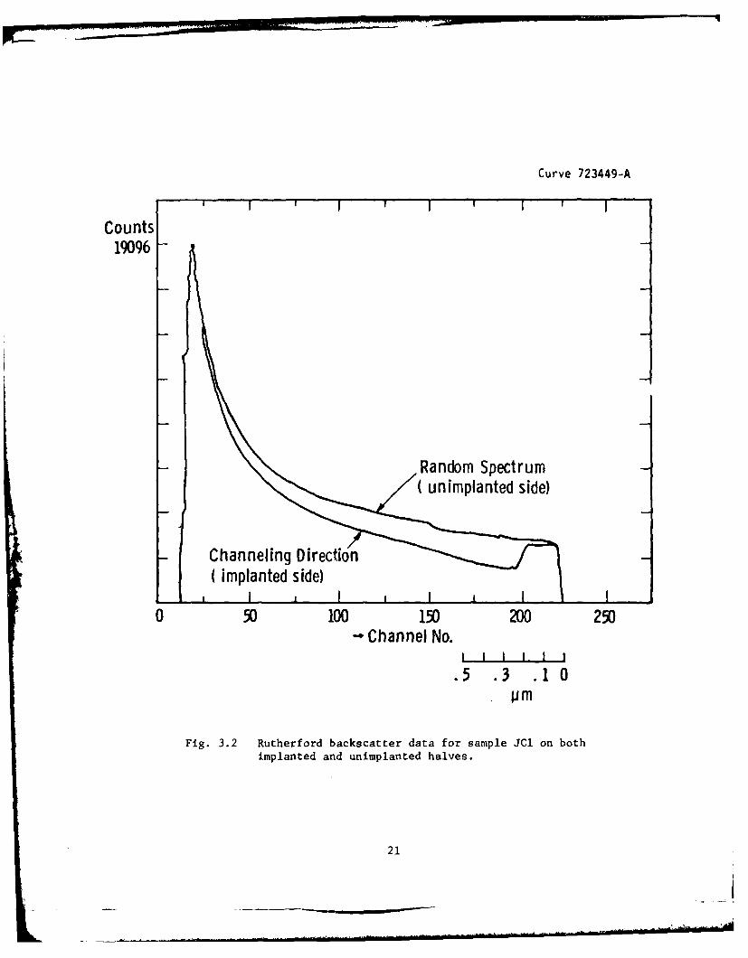
Samples JCl-JC6 were the first group implanted. Figure 3.2
is representative of the Rutherford Backscattering (RBS) data collected
for these samples. The backscatter data in a "random" direction is
18
Table 3.1
Review of Amorphization Implant Conditions
Sample No. Fluence Energy Cap Sample Temp.(Before Implant) Sml ep
JCl 5 x 10¹⁴ 200 keV --- 300 0K
JC3 1 x lo15 200 keV 300 0K
JC4 i x 1015 200 keV --- 300 0K
JC5 1 x 10¹⁵ 200 keV 300 0K
JC6 2 x 10¹⁵ 200 keV --- 300 0K
A 1 x 101l 200 keV 770K
B 1 x 10¹⁵ 200 keV ooo0 Si3N4 300 0K
C 1 x 10¹⁵ 200 keV i00OX Si3N4 770K
1 x 10¹⁵ 200 keV 300 0K
indicative of a disordered crystal. When the data is taken on an un-
damaged crystal in a so-called "channeling" direction, the reflected
beam is smaller than the random beam reflection. Thus, an implanted
sample analyzed in a channeling direction will give a measure of the
damage level relative to the two previously described extremes. We
define amorphization as damage at the level of random backscatter.
Referring to Fig. 3.2, the damage from a phosphorus 5 x 1014 cm-2
implant essentially accomplishes amorphization of the InP lattice.
Amorphization was also observed for the other samples in this series
(JC3, 4, 5 and 6).
Recrystallization experiments were aimed at observing the low
temperature solid phase reordering previously described for Si. By
scaling the 550C anneal temperature used in the Si work to the melting
point of Si, a 400C anneal temperature was chosen for InP. While this
temperature is a significant reduction from the 700C anneals tradi-
tionally used for low damage InP implantation, it is still enough to
19

Dwg. 7727A94
200kV
InP
Fig. 3.1 Schematic representation of "masked" InP sampleduring implantation.
20
Curve 723449-A
Counts19096
Random Spectrum(unimplanted side)
Channeling Direction(implanted side)
0 50 100 150 200 250Channel No.
.5 .3 .1 0. Pn
Fig. 3.2 Rutherford backscatter data for sample JCl on bothimplanted and unimplanted halves.
21
promote thermal decomposition of the InP for the long (24 hr) times
contemplated for the solid phase regrowth. Two possibilities for pro-
tecting the InP are PH3 overpressures (capless anneals) or dielectric
capping. Plasma deposited Si3N4 was chosen as a cap for the 400'C
anneal. The AZ mask was stripped from the samples and deposition was
performed at 340'C for 15 minutes to obtain 100OX of Si3N4 . This
nitride is conventionally used as a cap for high temperature annealing
of GaAs (860*C), and hence is of a proven quality. Twenty-four hour
anneals of these samples failed to re-order the damaged region. Other
workers in GaAs have observed that room temperature high dose implants
have self-annealed the amorphized sample such that it does not undergo
the sought after solid phase epitaxy. 6 In addition, there was some
question as to the viability of capping after the implant, i.e. is
there an intermediate contamination? In an effort to remove some of
these questions, sample series A to D was run. The "capped" samples
had Si3N4 over the half of the InP to be implanted, and Ak over the
other half. A liquid nitrogen cold stage was used on samples A and C
to try and minimize any self annealing during the high dose implant.
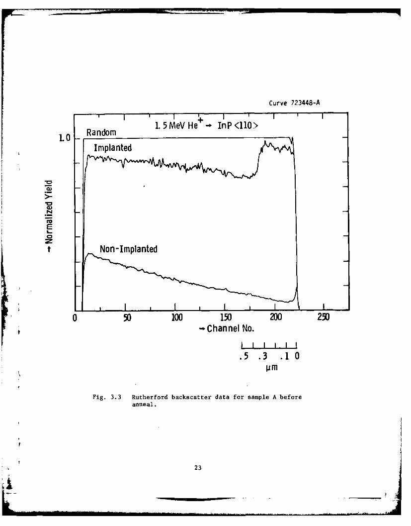
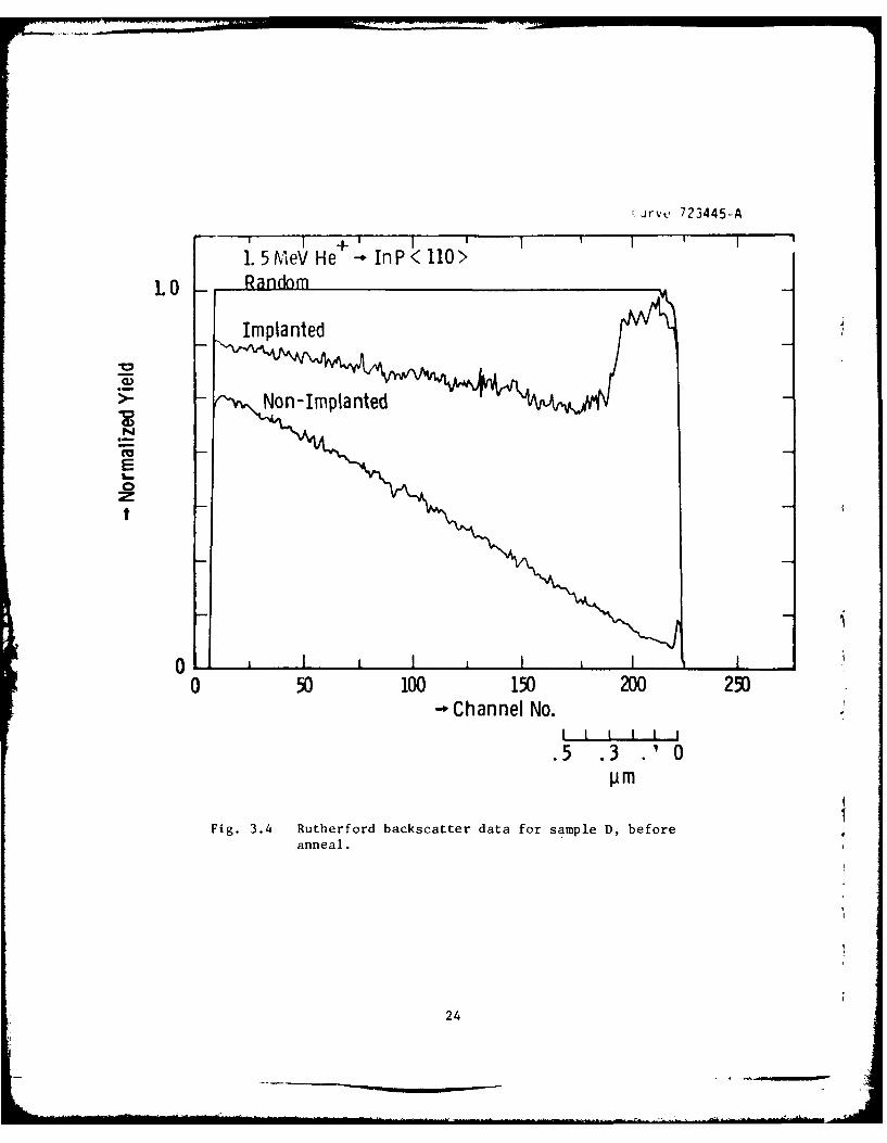
Samples B and C (implant through Si3N4 ) showed surface deteri-
oration from the implant which prohibited further measurement. Figures
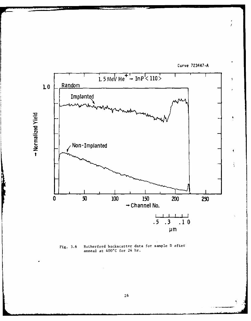
3.3 and 3.4 represent the backscatter data for A and D, respectively.
The effective width of the amorphized region on sample A is larger than
D. This gives a measure of the self-annealing which takes place for
the 1 x 10¹⁵ implant between a liquid nitrogen temperature implanted
sample (A) and a room temperature implant (D). Both samples were capped
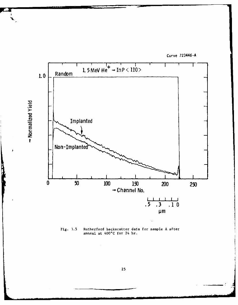
and annealed for 24 hr at 400C as previously described. Figures 3.5
and 3.6 show the backscatter profiles for A and D, respectively, after
cap, anneal and stripping of the cap. The key result from this experi-
ment is that by minimizing the self-annealing during implantation, it
becomes possible to observe the low temperature re-ordering. Sample D
does show some reduction in the width of the amorphized region, but
clearly sample A has had a return to crystallinity.
22
Curve 723448-A
LO Random1. 5MeV He + InP(110>
Rpanom
0 50 100 150 200 250-.Channel No.
.5 .3 .1 0
Fig. 3.3 Rutherford backscatter data for sample A beforeanneal.
23
lirve 723445-A
1. 5MeV He -In P <lLO Rno
Nopln-Imlate
2
E
I-
0
0 5) 100 150 200 25)-.$Channel No.
.5 .3 2 0
Fig. 3.4 Rutherford backscatter data for sample D, beforeanneal.
24
Curve 723446-A
1.0 Rndom L 5MeV He+ -InPK110>
1.0mpRandom
NnImplanted
0 50 100 150 200 250-*Channel No.
.5 .3 .1 0
Fig. 3.5 Rutherford backscatter data for sample A afteranneal at 400%C for 24 hr.
25
Curve 723447-A
1.5MeVHe -InP<110>L0 Random
Non-Implanted
tL
0 50 100 150 200 250-+Channel No.
IL I I I 1
.5 .3 .10oPm
Fig. 3.6 Rutherford backscatter data for sample D afteranneal at 400%C for 24 hr.
26

Work remains in identifying any electrical ramifications of
the amorphized crystal. In particular, the initial hypothesis was that
higher dopant incorporation is possible for implants of this nature.
This conjecture remains to be proved. Additionally, Fig. 3.5 shows
some residual damage remaining in the annealed InP. This represents
possible scattering centers and hence transport degradation is a possi-
bility. For the device of interest, it ultimately may turn out that
this damage degrades the active channel of the FET. It should be
pointed out that this approach extends itself to active layer prepara-
tion as well. Hence, one could envision a "deep" phosphorus damage
implant followed by Si and Mg implants to create the device structure.
The initial recrystallization work is encouraging and offers the possi-
bility of a low anneal temperature implant technology for InP which
obviates traditional capping failures at high temperature.
27

4. DEVICES
The previous section reviewed an initial study aimed at
bringing ion implantation technology to bear on InP JFET Fabrication.
A parallel effort was maintained to develop a diffused-junction gate
technology. The following sections review the p-n junction technology,
the JFET Fabrication sequence and rf performance, and concludes with a
semi-quantitative comparison between comparable GaAs and InP FET's.
4.1 Diffused Junction Technology
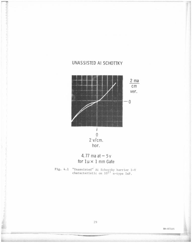
Figure 4.1 shows the I-V characteristics of an "unassisted"
At Schottky gate on n-type InP. Our previously reported work at over-
coming the inherent low barrier heights on InP by using various dielec-
tric layers between the gate and the InP was marginally successful.
The desirability of a reproducible gate system ultimately weighed
against the dielectric assisted barriers and in favor of p-n junctions.
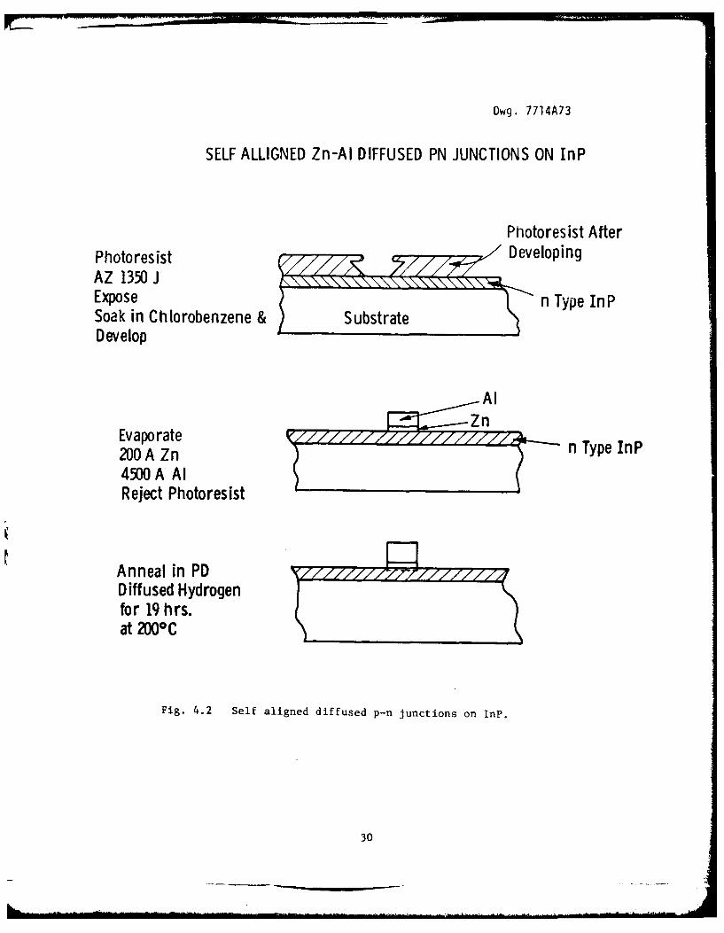
The idea of the diffused junction gate is to define the gate region
using traditional deposition and lift techniques followed by an anneal-
ing step to produce the junction. Figure 4.2 schematically represents
the steps involved in defining micron length p-n junctions. The sur-
face metal is intended to provide an "ohmic" contact to the diffused
semiconductor as well as capping the dopant species against evaporation
from the sample. There should be no "phase" interference between the
two elements associated with the anneal, and in addition, the surface
metal should be a slow diffuser relative to the dopant. The group II
elements (Mg, Cd, Zn) are the recognized choices for producing p-type
doping in InP. Other workers havre tried combinations like Au-Mg or
Au-Zn to satisfy the aforementioned criteria. Neither choice has been
successful; in the Mg-Au case the Mg tends to oxidize and hence yields
non-reproducible results, while the Au-Zn system suffers from the
28
Dwg. 7714A73
SELF ALLIGNED Zn-Al DIFFUSED PN JUNCTIONS ON InP
Photoresist AfterPhotoresist DevelopingAZ 1350 JExpose n Type InPSoak in Chlorobenzene & SubstrateDevelop
Al
Evaporate200 A Zn n Type InP
4500 A AIReject Photoresist
Anneal in PDDiffused Hydrogenfor 19 hrs.at 2000 C
Fig. 4.2 Self aligned diffused p-n junctions on InP.
30
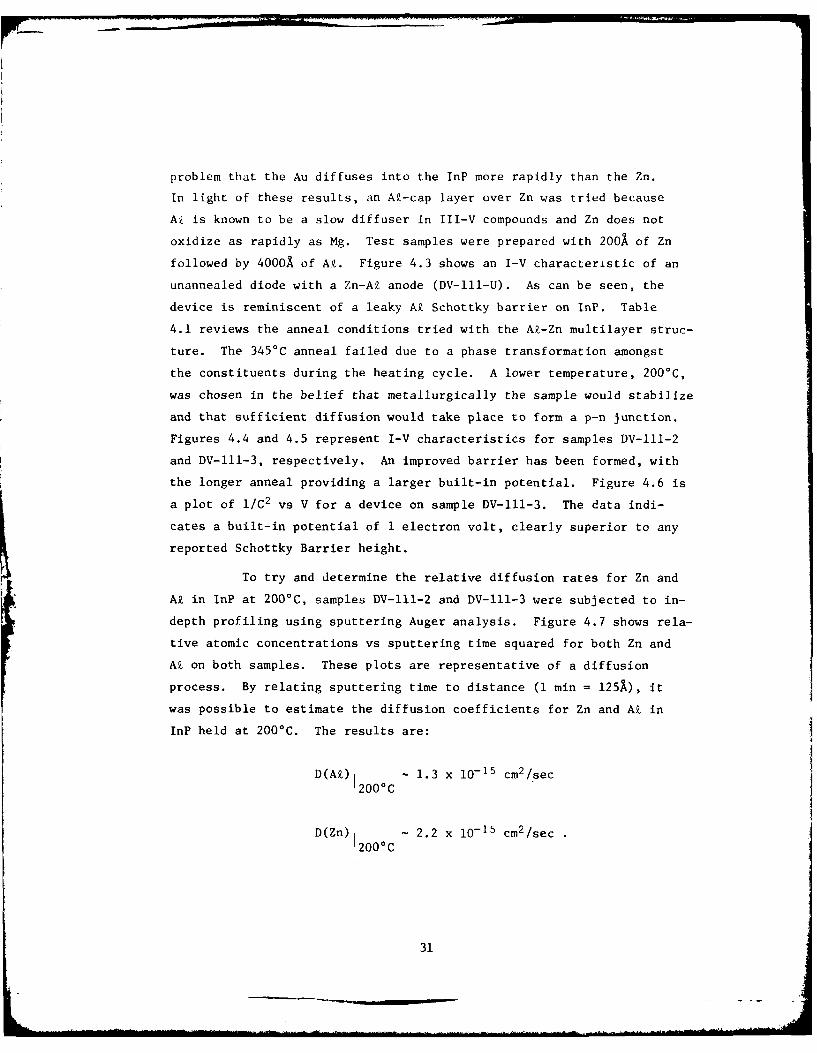
problem that the Au diffuses into the InP more rapidly than the Zn.
In light of these results, an AZ-cap layer over Zn was tried because
AZ is known to be a slow diffuser in III-V compounds and Zn does not
oxidize as rapidly as Mg. Test samples were prepared with 200X of Zn
followed by 4000 of At. Figure 4.3 shows an I-V characteristic of an
unannealed diode with a Zn-At anode (DV-lll-U). As can be seen, the
device is reminiscent of a leaky At Schottky barrier on InP. Table
4.1 reviews the anneal conditions tried with the At-Zn multilayer struc-
ture. The 345°C anneal failed due to a phase transformation amongst
the constituents during the heating cycle. A lower temperature, 200°C,
was chosen in the belief that metallurgically the sample would stabilize
and that sufficient diffusion would take place to form a p-n junction.
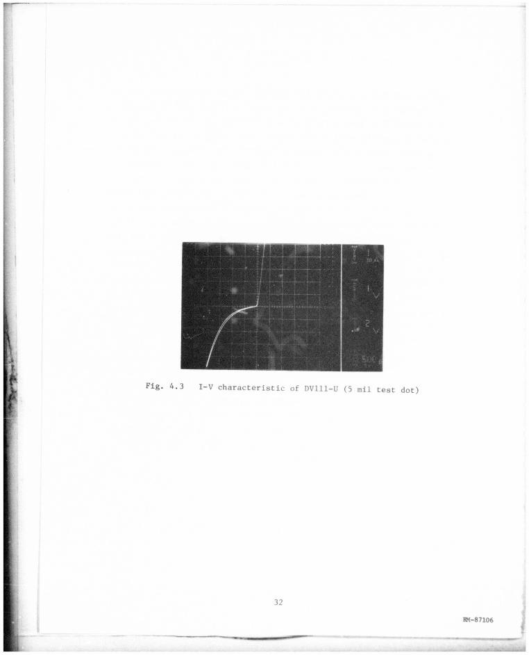
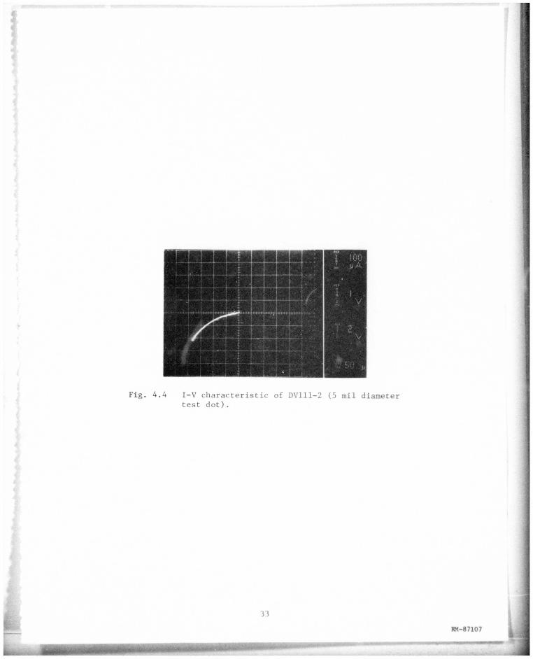
Figures 4.4 and 4.5 represent I-V characteristics for samples DV-111-2
and DV-III-3, respectively. An improved barrier has been formed, with
the longer anneal providing a larger built-in potential. Figure 4.6 is
a plot of 1/C2 vs V for a device on sample DV-lll-3. The data indi-
cates a built-in potential of I electron volt, clearly superior to any
reported Schottky Barrier height.
To try and determine the relative diffusion rates for Zn and
At in InP at 200*C, samples DV-111-2 and DV-111-3 were subjected to in-
depth profiling using sputtering Auger analysis. Figure 4.7 shows rela-
tive atomic concentrations vs sputtering time squared for both Zn and
At on both samples. These plots are representative of a diffusion
process. By relating sputtering time to distance (1 min = 125X), it
was possible to estimate the diffusion coefficients for Zn and At in
InP held at 200*C. The results are:
D(A)i 200oC - 1.3 x 10- 15 cm2 /sec
D(Zn) -2000C - 2.2 x 10⁻¹⁵ cm2 /sec
31
Curve 720828-A
1/C2 vs. V FOR Zn-Al DIODE ALLOYED AT 2000 C FOR 19 Hrs.
3 x 10
2 2x10²CNJ
cc)M
-10 1 23Reverse Voltacie (volts)
Fig. 4.6 1/C2 VS V for Zn-Ak Diode Alloyed at 200%C for 19 hr (sampleDVlll-3).
ij 35
Curve 722568-A
AUGER MEASUREMENTS OF AL & Zn DIFFUSION CONCENTRATION AS A
FUNCTION OF DISTANCE FOR SAMPLES HELD AT 20°C for 4. 5 and 19 hrs.
100
AlAI
19 Hrs. at 2000c C
"E - 4 1/ 2 Hrs. at 2000°CL.4-
(0 x~) =Csl(t) exp (- DZZn
For 200° C_DA= L 3x 1015cm2Isec
Dzn-- 2. 2x 101 cm2/sec
1 I I I II
0 200 400 600 800 1000 1200 .
X2 (Arbitrary Units)
Fig. 4.7 Auger measurements of A9. and Zn diffusion concentration as a
function of distance for samples held at 200C for 4.5 and
19 hr.
36
Table 4.1
Anneal Conditions for AZ-Zn Diffused Junction Test Structures
Sample Zn/Ak Anneal AnnealNo. Thickness X Temp. Time
DV-111-1 200/4000 345 0C 3 min
DV-111-2 200/4000 2000 C 4.5 hr
DV-111-3 200/4000 200 0C 19 hr
DV-Ill-U 200/4000 -
These estimates are important for two reasons. First, they confirm the
supposition that Zn will diffuse more rapidly into InP than Ak. More
importantly, the diffusion coefficients permit a first calculation of
the lateral spreading of a diffused gate device. Taking one diffusion
length as a measure of the junction spreading on each side for a 19 hr
anneal, one gets a figure of approximately 0.1 wm per side junction
spreading. Current photolithographic limits are on the order of 1 Pm
geometries, hence a gate lifted off to a one micron dimension will have
an electrical length of 1.2 vim for the annealing sequence just outlined.
Thus, device performance comparisons between this type of JFET and a
MESFET should acknowledge reasonable "scaling" parameters associated
with gate lengths.
4.2 InP DJFET Fabrication and Performance
One of the attractive features of the diffused junction FET
(DJFET) is that it requires only slight modification of the processing
sequence for a Schottky barrier FET. Figure 4.8 is the established
process sequence for an "oxide assisted" InP MESFET, and Fig. 4.9 is
the modified fabrication sequence for the DJFET. Changes in the second
and third mask steps represent an improvement in photoresist lifting
technology and do not relate to any device design changes. The diffu-
sion step in the DJFET process is accomplished at a low enough tempera-
ture that the ohmic contacts are left undisturbed.
37
4k A_ _
Dwg. 7695A46
REALIGNED InP FET FABRICATION
" First Mask - IsolationPhotoresist - AZ ill - ExposeEtch InP -lgm H1 3 : 19cc H2O0
* Second Mask - Ohmic Contacts Sio 2 MetalSputter 5000 A Sio 2Photoresist - AZ 111 - Expose flIon Mill + Chemical Etch SiO2 nMetallize and Reject n
600 A Au Ge600A Pd
3500 A A uAlloy 4600C for 15 sec
* Third Mask - Channel ThinningPhotoresist - AZ 1350J - ExposeChemical Etch S102
Etch lnP -lgm HIO: 19cc HO n
" Fourth Mask - GatePhotoresist - AZ 1350J - Expose GatePlasma Oxidize SampleCr/Au Evaporation n_____________Reject Metal n
Fig. 4.8 Realigned InP FET fabrication sequence using oxide assistedgate.
38

Dwg. 7710A72
REALIGNED InP JFET FABRICATION
First Mask - IsolationPhotoresist - AZ 111 - ExposeEtch InP - 1gm Hl0 3: 19cc H20 M t ht rss
Second Mask - Ohmic ContactsPhotoresist - AZ 1350.i-ExposeSoak in Chlorobenzene &nDevelop l- kMetallize and Reject hIP nBfe
600 A Au Ge nBfe600 A Pd
3500 A AuAlloy 4600C for 15 sec
Thinned ChannelThird Mask - Channel Thinning
Photoresist - AZ1350J-ExposeEtch InP-lgm HIO03:l19cc H 20 ZIIIII
In P
Fourth Mask - Gate ______Gat
Photoresist - AZ1350J-Expose _______Lt_____
Soak in Chlorobenzene &DevelopMetallize and Reject200 A Zn4500OA AlAnneal at 2000C for 19 hrs.
Fig. 4.9 Realigned TnP DJFET fabrication.
39
Wafers were thinned to 4 mils thickness using grit lapping,
and the backside was metallized using Ti/Au/Ni/Au. The wafers were
sawed, and individual devices were soldered to microwave headers using
Au-Sn solder. Final wire bonding was accomplished on a heated stage
thermo compression bonder. It is important to note that the device
characteristics were left unchanged as a result of these final assembly
steps. Because of the extremely small Zn diffusion coefficient at
200*C, it would require long term operation of the device near this
temperature to effect significant channel degradation. Thus, the dif-
fused gate device offered a reasonable vehicle for observing the poten-
tial performance of an InP JFET, both for small signal and power
performance at microwave frequencies.
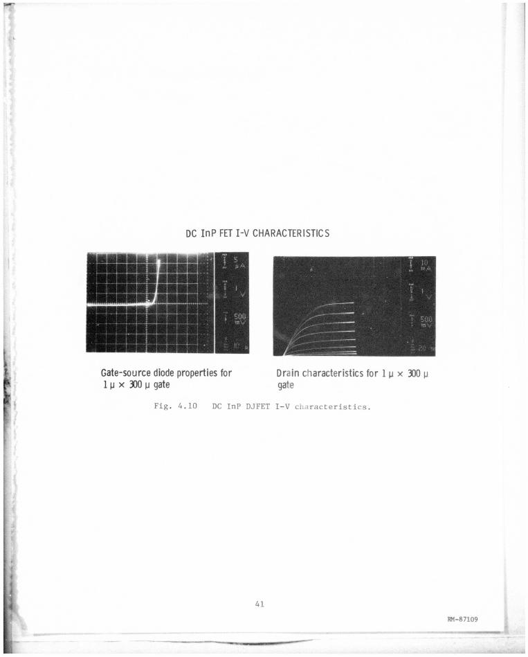
Figure 4.10 shows a DC I vs V characteristic of a 300w DJFET
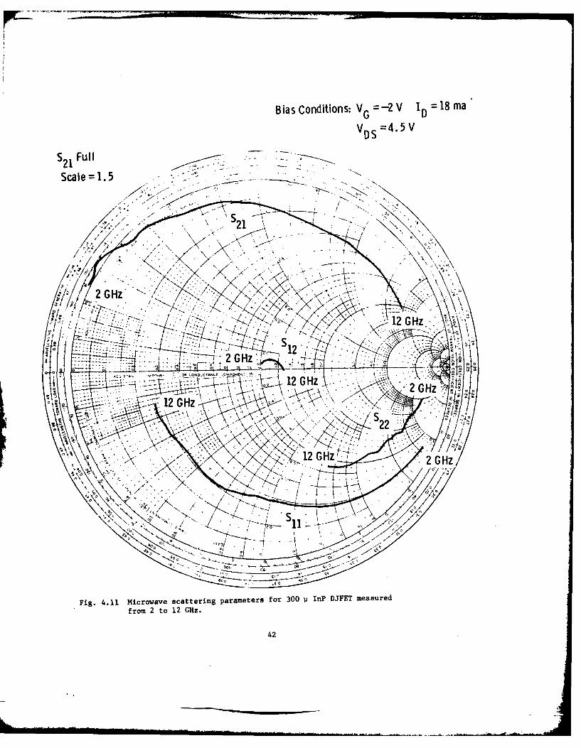
along with its associated gate-source performance. Figure 4.11 shows
the scattering parameters measured for an InP DJFET of 300jperiphery.
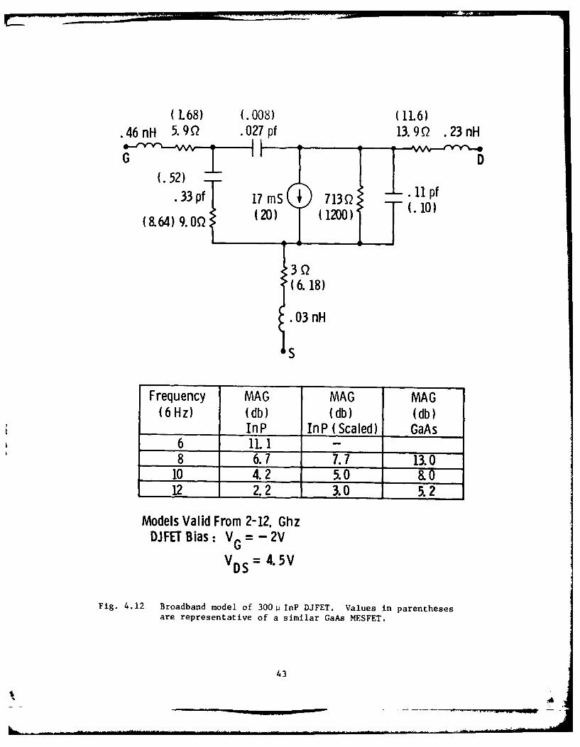
Figure 4.12 is a small signal lumped element equivalent circuit for the
same device. Shown in parenthesis are representative values for a
similar GaAs MESFET. It should be noted that most of these lumped ele-
ment values are bias sensitive.
There are several interesting aspects to the equilvalent cir-
cuit of Fig. 4.12. The input resistance of both the InP and GaAsf
devices is on the order of 17 Q. Also, the transconductance, gm' and
output capacitance, CDS, are comparable for both devices. The major
difference between the two devices is found in the gate to drain
feedback capacitance, Cgd, and the output conductance. Both of these
elements are more favorable in the GaAs FET. A more detailed discus-
sion of Cgd is provided in the following section.
No two devices will be "identical." Here, for example, it
can be seen that the gate-source capacitance is larger in the GaAs
device than the InP device. By comparing these capacitances and the
relative bias points for both devices, it was deduced that the GaAs
device was doped approximately 58% higher than the InP device. Thus,
it is anticipated that the higher doping would boost the gm of the GaAs
40
Bias Conditions: V G =-2V ID =18 ma
V DS= 4.5 V
S1 Full
Scale 1. 5-
/S21
- /ro/
tl I-V'E Q OOCTNEot4. 2 G Hzz
0 .0
from~1 2 o 2 z
422
(L68) (.008) (11.6).46nH 5.9Q .027 pf 13.90 .23 nH
(.52)1. 1 f.33 pf 1rn ms 713Q (.10)
(&64) 9. OQ (20) (1200)
39
(6. 18)
.03 nH
S
Frequency MAG MAG MAG(6 Hz) (clb) (db) (db)
InP InP (Scaled) GaAs6 11. 1-8 6.7 7.7 13.0
10 4.2 5.0 &12 2.2 3.0 5.2
Models Valid From 2-12. GhzDJFET Bias : V G = -2V
V DS = 4.5V
Fig. 4.12 Broadband model of 3OOi InP DJFET. Values in parenthesesare representative of a similar GaAs MESFET.
43
device relative to the InP device independently of material parameters.
In addition, because of material differences between InP and GaAs,
identical bias conditions do not necessarily reflect physically similar
field geometries in two devices, hence comparisons are difficult. We
shall return to this point in the next section. For now, we note that
Fig. 4.12 includes scaled values for MAG which are indicative of the
performance anticipated for the same device with an electrical gate
length of lj instead of the 1.2p length estimated for side diffusion.
This scaling was done to allow a more meaningful comparison to the
gain performance of the ip GaAs FET.
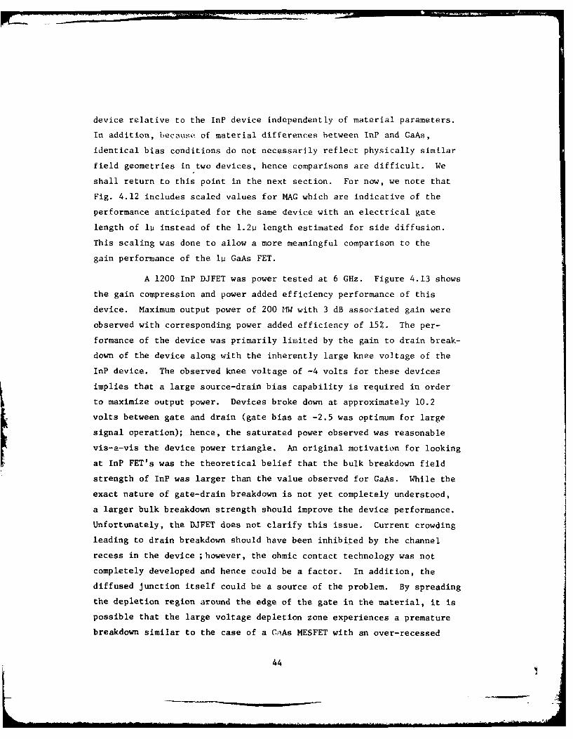
A 1200 InP DJFET was power tested at 6 GHz. Figure 4.13 shows
the gain compression and power added efficiency performance of this
device. Maximum output power of 200 ?W with 3 dB associated gain were
observed with corresponding power added efficiency of 15%. The per-
formance of the device was primarily limited by the gain to drain break-
down of the device along with the inherently large knee voltage of the
InP device. The observed knee voltage of -4 volts for these devices
implies that a large source-drain bias capability is required in order
to maximize output power. Devices broke down at approximately 10.2
volts between gate and drain (gate bias at -2.5 was optimum for large
signal operation); hence, the saturated power observed was reasonable
vis-a-vis the device power triangle. An original motivation for looking
at InP FET's was the theoretical belief that the bulk breakdown field
strength of InP was larger than the value observed for GaAs. While the
exact nature of gate-drain breakdown is not yet completely understood,
a larger bulk breakdown strength should improve the device performance.
Unfortunately, the DJFET does not clarify this issue. Current crowding
leading to drain breakdown should have been inhibited by the channel
recess in the device ;however, the ohmic contact technology was not
completely developed and hence could be a factor. In addition, the
diffused junction itself could be a source of the problem. By spreading
the depletion region around the edge of the gate in the material, it is
possible that the large voltage depletion zone experiences a premature
breakdown similar to the case of a OaAs MESFET with an over-recessed
44
15 , F T 1 1 1 1 -- I I j 1- 100
75
10
50
C --5-
25
0 ,0
0 5 10 15 20 25 30Output Power (dbmr)
V(O0 = -2.50v V (0) =7.70v 6.0GHz
Fig. 4.13 InP DJFET (1200w periphery) tuned for power at 17 dbm.
45
gate. This problem could potentially be alleviated by going to a more
sophisticated process where a uniform p-layer is created over the n-
layer, and then the p-layer is removed everywhere except for the gate
region. Thus, InP JFET device design requires more study to optimize
the device toward its ultimate capability. Despite the non-optimum
nature of the DJFET studied, it is still possible to draw some conclu-
sions regarding the viability of InP for microwave FET applications.
The following section is aimed at refining the comparison between the
GaAs and InP transistors.
4.3 Comparison Between InP DJFET and GaAs MESFET
One of the key areas of controversy regarding the viability
of high frequency InP FET's has been the previously observed large gate-
drain feedback capacitance in InP MESFET's. The feedback between gate
and drain is possible both via the active channel and the substrate.
Initial hypothesis comparing the InP and GaAs devices relied upon the
active channel mechanism. In particular, it was believed that strong
Gunn domain formation at the drain edge of the gate in the GaAs device
"de-coupled" the active channel feedback path. InP, with an acknowledged
smaller negative differential mobility than GaAs, was conversely believed
to have little or no domain formation in the channel, hence, Cgd for InP
would be larger in InP than GaAs. Alternatively, if one believed that
the capacitive feedback was a substrate phenomenon, a totally different
conclusion could be drawn. Cr doped InP, which was used in the initial
InP MESFET study, was about four orders of magnitude more conductive
than its GaAs counterpart. It was therefore easy to envision a different
model in which a "depletion-like" capacitive link is established between
the gate-drain bus pads through the substrate. In the intervening time
since the initial InP MESFET study, Fe doping of InP has led to sub-
strates whose conductivity is close to that of Cr doped GaAs. Thus, one
feedback mechanism has been removed from the problem and conceivably
allows a clearer look at the issue.
46
The lnP DJFET offers no change in feedback mechanisms from
the MESFET, hence, it is valid to compare the lnP DJFFT Cg d feedback to
the GaAs MESFET C feedback.gd
To begin the comparison, it is important to realize the sig-
nificance of Cgd in determining device performance. Referring to Fig.
4.12 it is clear that Cgd in the InP DJFET is larger by a factor of
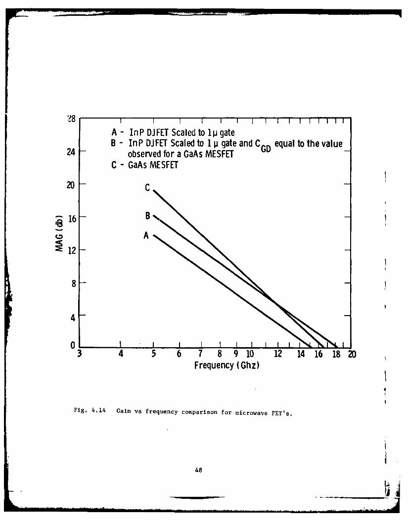
three than Cgd in its counterpart, the GaAs MESFET. Figure 4.14 con-
tains three gain plots which put the importance of Cg d in perspective.
Curve A represents the gain of the InP DJFET of Fig. 4.12 with the
gate length scaled to 1i. Curve C is the gain for the GaAs MESFET in
the same figure, and Curve B is the InP DJFET of A but with its Cg d
value of 0.027 pf replaced with the GaAs value of 0.008 pf. The DJFET
performance suffers by 2 db due to the Cgd value at the bias point
tested.
Since a large signal model can be thought of as a combination
of small signal models along the power tuned load line, it is instruc-
tive to characterize the DJFET at many bias points. Figure 4.15 shows
a family of curves for Cgd for a 30011 InP DJFET as a function of gate
bias with drain bias as a parameter. In contrast, Fig. 4.16 shows a
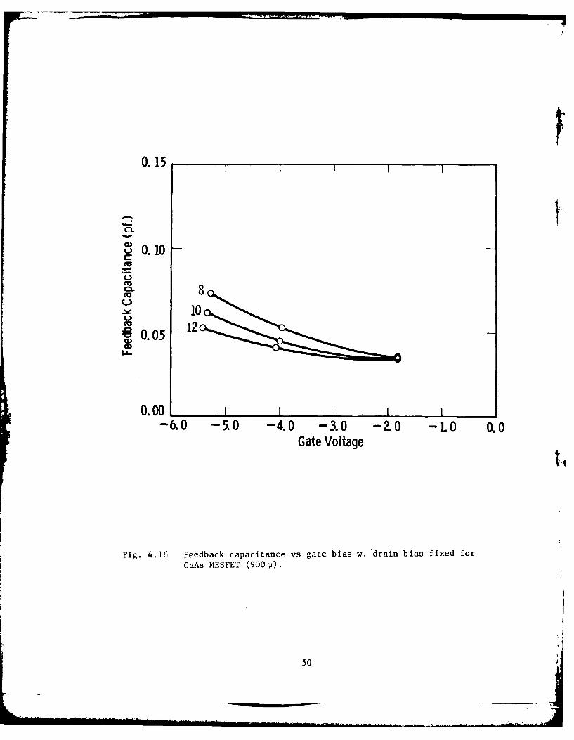
similar family of curves for a 900p GaAs MESFET. Clearly, the behavior
of Cgd with bias is different for the two devices. The InP DJFET has
a feedback capacitance which is "depletion-like" in character, while
the GaAs MESFET is opposite in nature.
No attempt at a simple relationship between the feedback
capacitance and substrate conductivity was possible; however, it is
clear that a fundamentally different mechanism is responsible for the
feedback behavior of the InP DJFET vis-a-vis the GaAs MESFET. The
averaged feedback capacitance of the InP DJFET along a "power" load
line will be higher than the ,_',um;.able GaAs device by a factor of
three. As seen in the gain relationship shown in Fig. 4.16, this
results in a sacrifice of several db of gain at X-band.
47
A - In P DJ FET ScalIed to 1 p gateB - In P DJFET Scaled to 1 p. gate and C GD equal to the value
24 -observed for a GaAs MESFETC - GaAs MESFET
20 -c
216 B'..
~12 A
8
4
03 4 5 6 7 89 10 12 14 16 1820
Frequency (Ghz)
Fig. 4.14 Gain vs frequency comparison for microwave FET's.
48

0.15
'a 3S0. 10
C)
S0.05 69
0.00 I-3.0 -2.0 -1.0 0.0
Gate Voltage
Fig. 4.15 Feedback capacitance vs gate bias w. drain bias fixed forInP DJFET (300 -p).
49
0.15
. .10C
CD-
.05
-~0.05
-6.0 -5.0 -4.0 -3.0 -ZO -LO 0.0Gate Voltage
Fig. 4.16 Feedback capacitance vs gate bias w. drain bias fixed forGaAs MESFET (900p).
50 1
The results of the comparison between the GaAs MESFET and
the InP DJFET are:
(1) Optimization and improved understanding of the InP DJFET are neces-
sary to improve the breakdown performance of the transistor in order to
allow large rf voltage swings.
(2) The inherently larger Cgd of InP compared to GaAs degrades the
gain of the device by several db. This will be a severe disadvantage
for an InP FET compared to a GaAs FET.
51

5. CONCLUSIONS AND RECOMMENDATIONS FOR FURTHER STUDY
As the previous chapter discussed in some detail, InP power
transistors appear to suffer some deficiencies vis-a-vis their GaAs
counterparts. These include the following points:
* large knee voltage
* low source-drain breakdown voltage
* large feedback capacitance.
While it is possible that further technological and device design re-
finements may be possible, we believe that InP microwave power transis-
tors will present a significant challenge before they may become
successful.
The work represented by this program filled in some key gaps
in the InP technology. Among the achievements are:
* Well characterized, multilayer vapor phase epitaxy
* N-type ion implantation
* Amorphization and low temperature recrystallizationstudies
* A reproducible etching technology
* A self aligned diffused junction gate on n-typematerial.
Additionally, as a result of this technology development, we were able
to successfully fabricate, test and analyze X-band InP JFET's. This
study shows serious technical problems facing further InP power device
development. Alternatively, we believe that InP technology may be
usefully employed in the digital logic arena. Successful MOS device
performance would allow the realization of logic gates using standard
MOS layouts from silicon technology. Thus, our recommendations for
further study would include:
52

r
* Reproducible ohmic contact development with specificcontact resistance <10 - 6 Q-cm
0 Further exploitation of initial ion implantationI.
amorphization studies - specifically directed atp-type implants
* Small signal device development and modeling atmicrowave frequencies to improve device design forswitching applications.
Successful completion of the above tasks would undoubtedly
aid the development of InP digital IC's. In addition, it should be
noted that substrate development will also be required. At present,+
semi-insulating or n InP is limited in supply and quite variable in
quality. Any successful exploitation of InP will ultimately require
a change in the availability of high quality material as well as
further device technology development.
53

F
6. REFERENCES
1. R. C. Clarke, A Study of the Molar Fraction Effect in the PC9 3-In-H 2System, J. Crystal Growth 23, 1974, pp. 166-168.
2. R. C. Clarke and W. D. Reed, Paper presented at Cornell Conferenceon Active Semiconductor Devices, Ithaca, New York, 1979.
3. J. V. Dilorenzo, Vapor Growth of Epitaxial GaAs: A Summary of Para-meters which Influence the Purity and Morphology of Epitaxial Layers,J. Crystal Growth 17, 1972, pp. 189-206.
4. M. C. Hales and J. R. Knight, The Electrical Properties of VaporEpitaxial Indium Phosphide Grown in the Presence of Oxygen, J.Crystal Growth 46, 1979, pp. 582-584.
5. Tsai and Streetman, "Recrystallization of Implanted AmorphousSilicon Layers," J. A Phys., January 1979.
6. Max Yoder, Office of Naval Research, private communication.
7. R. W. H. Engelmann and C. A. Liechti, Bias Dependence of GaAs andInP MESFET Parameters, IEEE Transactions on Electron Devices,Vol. 24, No. 11, November 1977.
54
7. ACKNOWLEDGMENTS
We would like to acknowledge the excellent technical assistance
of Joseph Kotvas, Elizabeth Halgas, Don Reed, Pat Kost, Sophie Maystrovich,
Carl Seiler, Herman Abt, and Clarence Zahrobsky in this program.
55
8. PRESENTATIONS
The following presentations and publications were partially
funded by contract number N00014-78-C-0254.
1. R. C. Clarke and W. D. Reed, "Vapor Phase Epitaxy of Indium
Phosphide for FET Fabrication," Proc. of Seventh Biennial Cornell
Electrical Engineering Conference, Cornell University, Ithaca,
New York, August 1979.
2. V. L. Wrick, J. C. Kotvas, R. C. Clarke, and E. T. Watkins,
"Self Aligned Diffused Junction InP FET's," paper presented at
1980 Workshop on Compound Semiconductors for Microwave Materials
and Devices, San Francisco, February 1980.
3. V. L. Wrick, W. J. Choyke, and C.F. Tzeng, "Amorphization and
Low Temperature Recrystallization of InP," paper submitted to
Solid State Electronics.
56