Embed Size (px)
Citation preview
TET4190
Power Electronics for Renewable Energy
Induction Heating with SiC Transistors
Mathew M'kandawire
Jiaying Wang
Tatjana Kalitjuka
Aleksejs Grigorjevs
Submission date: 29.10.2010
Supervisor: Tore Marvin Undeland, ELKRAFT
Co-supervisor: Langelid John Kåre, EFD Induction
Norwegian University of Science and Technology
Department of Electrical Power Engineering
2
ABSTRACT
Silicon Carbide (SiC) electronic devices have demonstrated the ability to function under
extreme high temperature, high frequencies and high power. This development will enable major
enhancements and improvements in the field of induction heating where high frequency and high
power are a requirement. An overview of SiC characteristics that make this material feasible for
use in high-voltage, high temperature and high frequency induction heating applications is
presented. The benefits of using SiC transistors instead of conventional Si transistors in modern
induction heating applications have been highlighted. This paper surveys actual companies that
deal with Silicon Carbide (SiC) power electronic devices and have commercially available
components to offer today. The paper also gives an overview on the research directions these
companies are heading for in the future and highlight which power electronic semiconductors
and in turn the technology itself seem to be in priority in the near future. Turn on and turn off
switching losses of a SiC JFET manufactured by SemiSouth was done in the laboratory using the
double-pulse testing method. The same testing was performed on ultra fast Si IGBT and the
results have been compared. The practical measurements are of importance in order to
understand the advantages of using SiC transistors and what improvements can be achieved in
industrial applications such as induction heating. These measurements were performed using
existing equipment in power electronics lab at NTNU.
3
CONTENTS
1. INDUCTION HEATING WITH SIC TRANSISTORS .......................................................... 4
1.1. Advantages of SiC electronics .......................................................................................... 5
1.2. High-Temperature device operation ................................................................................. 5
1.3. High-Power device operation ........................................................................................... 5
1.4. Higher efficiency .............................................................................................................. 6
1.5. System benefits of High-Power and High-Temperature SiC devices .............................. 6
2. COMPANIES MANUFACTURING SIC POWER ELECTRONIC DEVICES .................... 7
3. POWER ELECTRONIC CONVERTERS FOR INDUCTION HEATING APPLICATIONS
8
4. PRACTICAL MEASUREMENTS .......................................................................................... 9
4.1. Introduction ...................................................................................................................... 9
4.2. Software description ....................................................................................................... 10
4.3. Principle of testing operation .......................................................................................... 11
4.4. Testing object description ............................................................................................... 12
4.5. Measurements and Instruments ...................................................................................... 12
4.6. DC link voltage investigation ......................................................................................... 14
4.7. Switching times .............................................................................................................. 15
4.8. Switching power losses and energies ............................................................................. 15
CONCLUSIONS ........................................................................................................................... 17
REFERENCES .............................................................................................................................. 18
4
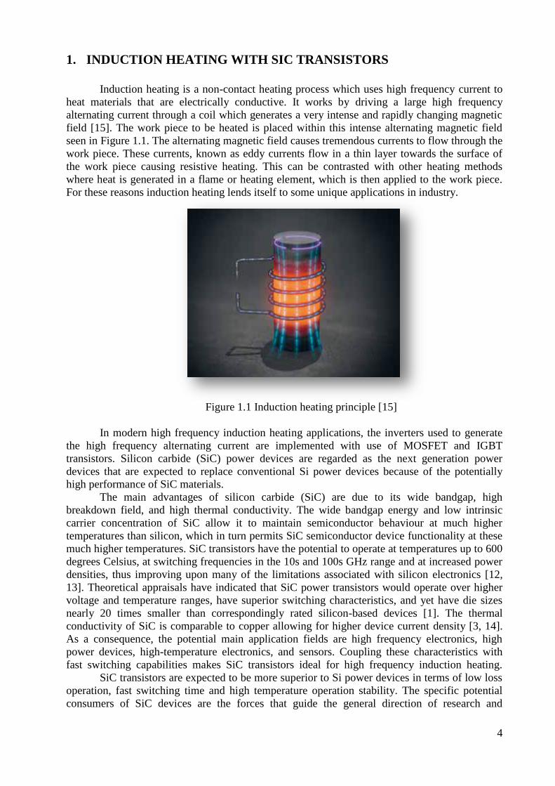
1. INDUCTION HEATING WITH SIC TRANSISTORS
Induction heating is a non-contact heating process which uses high frequency current to
heat materials that are electrically conductive. It works by driving a large high frequency
alternating current through a coil which generates a very intense and rapidly changing magnetic
field [15]. The work piece to be heated is placed within this intense alternating magnetic field
seen in Figure 1.1. The alternating magnetic field causes tremendous currents to flow through the
work piece. These currents, known as eddy currents flow in a thin layer towards the surface of
the work piece causing resistive heating. This can be contrasted with other heating methods
where heat is generated in a flame or heating element, which is then applied to the work piece.
For these reasons induction heating lends itself to some unique applications in industry.
Figure 1.1 Induction heating principle [15]
In modern high frequency induction heating applications, the inverters used to generate
the high frequency alternating current are implemented with use of MOSFET and IGBT
transistors. Silicon carbide (SiC) power devices are regarded as the next generation power
devices that are expected to replace conventional Si power devices because of the potentially
high performance of SiC materials.
The main advantages of silicon carbide (SiC) are due to its wide bandgap, high
breakdown field, and high thermal conductivity. The wide bandgap energy and low intrinsic
carrier concentration of SiC allow it to maintain semiconductor behaviour at much higher
temperatures than silicon, which in turn permits SiC semiconductor device functionality at these
much higher temperatures. SiC transistors have the potential to operate at temperatures up to 600
degrees Celsius, at switching frequencies in the 10s and 100s GHz range and at increased power
densities, thus improving upon many of the limitations associated with silicon electronics [12,
13]. Theoretical appraisals have indicated that SiC power transistors would operate over higher
voltage and temperature ranges, have superior switching characteristics, and yet have die sizes
nearly 20 times smaller than correspondingly rated silicon-based devices [1]. The thermal
conductivity of SiC is comparable to copper allowing for higher device current density [3, 14].
As a consequence, the potential main application fields are high frequency electronics, high
power devices, high-temperature electronics, and sensors. Coupling these characteristics with
fast switching capabilities makes SiC transistors ideal for high frequency induction heating.
SiC transistors are expected to be more superior to Si power devices in terms of low loss
operation, fast switching time and high temperature operation stability. The specific potential
consumers of SiC devices are the forces that guide the general direction of research and
5
development. There are many potential markets for SiC devices, both long and short term, as
well as a host of immediate markets.
The future of SiC transistor is very promising because of its smaller size, lower loss,
higher efficiency, and easier heat dissipation. These are the characteristics required for new
generation power devices. However, these tremendous theoretical advantages are yet to be
widely realized in commercially available SiC transistors, primarily owing to the fact that SiC
device fabrication technologies are not yet sufficiently developed to the degree required for
reliable incorporation into most electronic systems.
This paper briefly explores the use of SiC transistor technology in induction heating
applications. A SiC JFET transistor was tested in the lab to investigate its switching loses using
the double pulse testing method. The results are compared to ones gained in the measurements
on fast Si IGBT. The projected performance benefits of SiC transistors are highlighted for
induction applications.
1.1. Advantages of SiC electronics
The utilization of SiC-based electronics offer the advantages of high-temperature, high-
power device operation and higher efficiency. The specific SiC device physics that enables high-
temperature, high-power and higher efficiency capabilities are discussed in details below.
1.2. High-Temperature device operation
The wide bandgap energy and low intrinsic carrier concentration of SiC allow SiC to
maintain semiconductor behaviour at much higher temperatures than silicon, which in turn
permits SiC semiconductor device functionality at much higher temperatures than silicon [2].
Semiconductor electronic devices function in the temperature range where intrinsic carriers are
negligible so that conductivity is controlled by intentionally introduced dopant impurities.
Furthermore, the intrinsic carrier concentration currents grow unacceptably large, and eventually
at still higher temperatures, the semiconductor device operation is overcome by uncontrolled
conductivity as intrinsic carriers exceed intentional device doping [3, 4]. The intrinsic carrier
concentration of silicon generally confines silicon device operation to junction temperatures
<300°C. SiC’s much smaller intrinsic carrier concentration theoretically permits device
operation at junction temperatures exceeding 600°C. The ability to place un-cooled high-
temperature semiconductor electronics directly into hot environments would enable important
benefits to induction heating applications. High-temperature capability eliminates performance,
reliability, and weight penalties associated with liquid cooling, fans, thermal shielding, and
longer wire runs needed to realize similar functionality in applications using conventional silicon
semiconductor electronics.
1.3. High-Power device operation
The high breakdown field and high thermal conductivity of SiC coupled with high
operational junction temperatures theoretically permit extremely high-power densities and
efficiencies to be realized in SiC devices. The high breakdown field of SiC relative to silicon
enables the blocking voltage region of a power device to be roughly 10x thinner and 10x heavier
doped, permitting a roughly 100-fold beneficial decrease in the blocking region resistance at the
same voltage rating [1]. Switching energy loss is often a function of the turn-off time of the
semiconductor switching device, generally defined as the time lapse between application of a
turn-off bias and the time when the device actually cuts off most of the current flow. In general,
the faster a device turns off, the smaller its energy loss in a switched power conversion circuit.
SiC’s high breakdown field and wide energy bandgap enable much faster power switching than
is possible in comparably volt–ampere-rated silicon power-switching devices. The fact that high-
6
voltage operation is achieved with much thinner blocking regions using SiC enables much faster
switching (for comparable voltage rating) in both unipolar and bipolar power device structures.
Therefore, SiC-based power converters could operate at higher switching frequencies with much
greater efficiency (i.e., less switching energy loss). Higher switching frequency in induction
heating is highly desirable because it permits use of smaller capacitors, inductors, and
transformers, which in turn can greatly reduce overall power converter size, weight, and cost [5].
1.4. Higher efficiency
The SiC’s smaller on-resistance and faster switching helps minimize energy losses and
heat generation, SiC’s higher thermal conductivity enables more efficient removal of waste heat
energy from the active device. Because heat energy radiation efficiency increases greatly with
increasing temperature difference between the device and the cooling ambient, SiC’s ability to
operate at high junction temperatures permits much more efficient cooling to take place, so that
heat sinks and other device-cooling hardware (i.e., fan cooling, liquid cooling, air conditioning,
heat radiators, etc.) typically needed to keep high-power devices from overheating can be made
much smaller or even eliminated. The high breakdown voltage and high thermal conductivity
coupled with high carrier saturation velocity allow SiC microwave devices to handle much
higher power densities than their silicon counterparts, despite SiC’s disadvantage in low-field
carrier mobility [6].
SiC-devices have excellent reverse recovery characteristics. With less reverse recovery
current, switching losses are reduced. As a result, there is no need to use soft-switching
techniques to reduce switching losses. Because of low switching losses, SiC devices can operate
at higher frequencies not possible with Si devices in power levels of more than a few tens of
kilowatts.
1.5. System benefits of High-Power and High-Temperature SiC devices
Uncooled operation of high-temperature and high-power SiC electronics would enable
revolutionary improvements to induction heating systems. SiC high-power solid-state switches
will also enable large efficiency gains in electric power management and control [7, 8].
Performance gains from SiC electronics could enable the public power grid to provide increased
consumer electricity demand without building additional generation plants, and improve power
quality and operational reliability through ―smart‖ power management. From the above
discussions it should be apparent that SiC high-power and high-temperature solid state
electronics promise tremendous advantages that could significantly impact converter drive
systems and power usage on a global scale. By improving the way in which electricity is used
SiC electronics promises the potential to better the daily lives of all citizens of the world SiC
transistors are expected to be more superior to Si power devices in terms of low loss operation,
fast switching time and high temperature operation stability.
The specific potential consumers of SiC devices are the forces that guide the general
direction of research and development. There are many potential markets for SiC devices, both
long and short term, as well as a host of immediate markets. The future of SiC transistor is very
promising because of its smaller size, lower loss, higher efficiency, and easier heat dissipation.
These are the characteristics required for new generation power devices.
7
2. COMPANIES MANUFACTURING SIC POWER ELECTRONIC
DEVICES
The main manufacturers that are of interest are Cree (USA), TranSiC AB (Sweden),
SiCED (Germany), SemiSouth (USA), Infineon (Germany), Rohm (Japan) and Powerex (USA).
These companies specialize in different fields of technology but have a common research and
development strategy – global adoption of Silicon Carbide-based power electronics. Despite the
common strategy every company try to focus on and commercialize a specific semiconductor
device, at least as far as SiC technology is concerned.
For example market’s leading innovator of semiconductor solutions Cree offer a wide
range of commercially available SiC Schottky diodes with voltage ratings from 600 V to
revolutionary 1700 V and current ratings from 1 A and up to 25 A. On the February 17 2009
Cree working together with both the United States Air Force Research Laboratory (AFRL)
Propulsion Directorate and high-power module pioneer Powerex, Inc., has developed a
demonstration dual switch 1200 V, 100 A power module featuring high-current SiC MOSFETs
and SiC Schottky diodes and capable of operating at junction temperatures up to 200 C° [1]. This
seems to be the first announcement of a viable SiC MOSFET which is still not available
commercially though. R&D center is concentrated on making an extensive research on SiC
MOSFET since these devices are normally-off devices and have drive requirements equivalent to
the silicon IGBT devices they replace, making the SiC module a potential drop-in replacement
for most applications. It is clear that by successfully selling SiC Schottky diodes the company is
further aiming on commercialization of SiC MOSFETs and these 1200 V, 100 A SiC MOSFET
modules, for instance, represent the next level of integration for SiC power devices into modern
power electronics world. It should be noted that in 2009 PET (Power Electronics Technology)
selected SiC power MOSFET by Cree as product of the year and highlighted a significant
product development. The popularity of SiC is also governed by the fact that a recent major
breakthrough in the development and wide scale commercialization of silicon carbide (SiC)
technology is achieved with the demonstration of high quality, 150-mm SiC substrates.
SemiSouth is a silicon carbide (SiC) based semiconductor company specializing in SiC
materials and electrical components for high-power, high-efficiency, harsh-environment power
management and conversion applications[1]. Unlike Cree, SemiSouth offers commercially
available and competitively priced SiC diodes, transistors and power modules. SiC Schottky
diodes are widely represented with a wide range of voltages, currents and configurations. Rated
currents of these devices reach values of 30 A, blocking voltages up to 1200 V and some of the
configurations include a double SiC Schottky chip in a common TO-247 package. SemiSouth is
the only manufacturer of Junction Field Effect Transistors (JFET) which is the tremendous
power device today. JFETs are manufactured both as normally-on and normally-off devices.
Normally-on JFETs are mainly represented with a SJDP120R085 model which has a blocking
voltage of 1200 V and has a relatively low on state resistance of 85 mΩ and uses a TO-247
package. Normally-off JFETs are represented with two 1200 V models, i.e. 100 mΩ
SJEP120R100 and 63 mΩ SJEP120R063 both in TO-247 package. A recently manufactured SiC
JFET, named the SJEP170R550 offers higher blocking voltage (1700 V), five times lower on-
resistance (550 m-Ohm), and approximately ten times lower output capacitance (COSS of 20 pF)
and gate charge (QG of 10 nC) compared with the best Si MOSFET technology.
Swedish semiconductor manufacturer TranSiC is among world leading developers and
manufacturers of the state-of-the-art Bipolar Power Transistors in Silicon Carbide (SiC). The
transistors are developed to meet the highest standards of power control in high temperature
environments as well as high efficiency operation in power electronics [1]. TranSiC realizes
compact high voltage SiC power transistors that offer the highest levels of efficiency yet suitable
for operations at very high temperature levels up to 250°C. The high temperature capabilities are
typically required for applications within the Oil & Gas and Avionics Industry. Power transistors

8
are also suitable for use in many switched power applications requiring high efficiency operation
for example such applications as hybrid vehicles, photovoltaic inverters, power factor correctors,
motor drives and mobile military radar units.
TranSiC successfully designs SiC power modules for high power applications. Recently a
three year development project supported by Vinnova and Energimyndigheten (the Swedish
Energy Agency) is realized. The aim of the project was to design and manufacture devices and
modules to enable energy efficient and compact power electronic systems. The goal of the
project was to verify the device designs for the proposed technology platforms, in particular
switching power designs has been reached. The results of the project include a state of the art
1200V SiC power module, consisting of six BitSiC power transistors and six diodes. The module
exhibits state of the art performance with on state losses of 1.15 V at 100 A and room
temperature. At an elevated temperature of 150°C, the TranSiC power module exhibits low
losses of 1.75 V at 100 A. Specific on-resistance of the module is at a very competitive 3.1
mΩ/cm2 at room temperature.
TranSiC’s power transistors have several benefits. The low on-state losses make it
possible to either use a transistor with smaller die, thus increasing the effective current density of
the system, or to use smaller and lighter cooling equipment. The fast switching speed enables the
system designer to use a higher switching frequency and reduce the size of the passive elements,
or to reduce the overall switching losses in the system.
3. POWER ELECTRONIC CONVERTERS FOR INDUCTION HEATING
APPLICATIONS
The most common converters for induction heating applications, which serve as standard
or universal converters, are either a half-bridge resonant inverter (Figure 3.1) or a full-bridge
resonant inverter (Figure 3.2). The main advantage of a resonant converter is that this converter
switches its status (from on to off and vice versa) when the voltage across it and/or a current
through it is zero at switching instant [2]. Thus transistor stresses and power losses are
minimized significantly.
The half-bridge inverter in its simplest form and is shown in Figure 3.1 [1]. It has two
identical dc voltage sources connected in series, two static switches, and two diodes. The diodes
are needed to protect the switches especially when these switches have to carry currents in the
reverse directions. Since most single-phase loads are inductive in nature, we have drawn the
circuit with an inductive load. Once the two large electrolytic capacitors are fully charged, they
behave as the voltage sources. The two equal resistors in parallel with the capacitors not only
ensure that the voltages on the two capacitor are the same but also provide the paths for the
capacitors to discharge once the half-bridge inverter is switched off.
Figure 3.1 Resonant load half-bridge inverter [1]
9
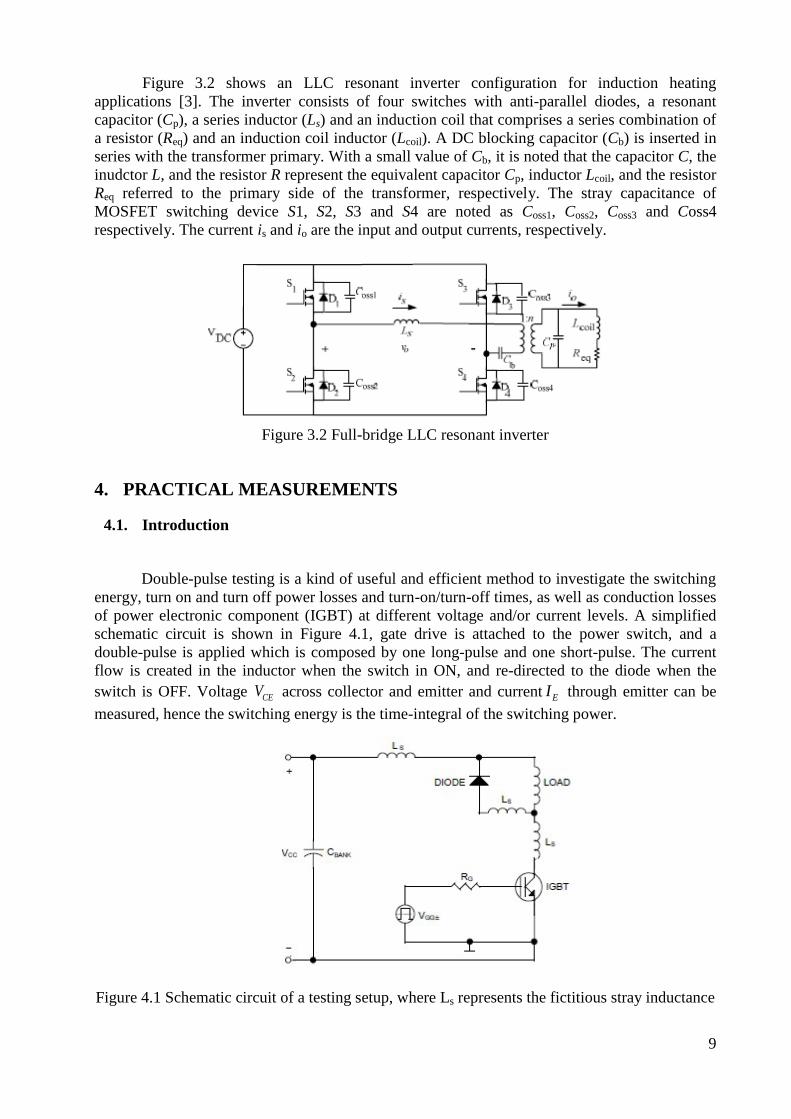
Figure 3.2 shows an LLC resonant inverter configuration for induction heating
applications [3]. The inverter consists of four switches with anti-parallel diodes, a resonant
capacitor (Cp), a series inductor (Ls) and an induction coil that comprises a series combination of
a resistor (Req) and an induction coil inductor (Lcoil). A DC blocking capacitor (Cb) is inserted in
series with the transformer primary. With a small value of Cb, it is noted that the capacitor C, the
inudctor L, and the resistor R represent the equivalent capacitor Cp, inductor Lcoil, and the resistor
Req referred to the primary side of the transformer, respectively. The stray capacitance of
MOSFET switching device S1, S2, S3 and S4 are noted as Coss1, Coss2, Coss3 and Coss4
respectively. The current is and io are the input and output currents, respectively.
Figure 3.2 Full-bridge LLC resonant inverter
4. PRACTICAL MEASUREMENTS
4.1. Introduction
Double-pulse testing is a kind of useful and efficient method to investigate the switching
energy, turn on and turn off power losses and turn-on/turn-off times, as well as conduction losses
of power electronic component (IGBT) at different voltage and/or current levels. A simplified
schematic circuit is shown in Figure 4.1, gate drive is attached to the power switch, and a
double-pulse is applied which is composed by one long-pulse and one short-pulse. The current
flow is created in the inductor when the switch in ON, and re-directed to the diode when the
switch is OFF. Voltage CEV across collector and emitter and current EI through emitter can be
measured, hence the switching energy is the time-integral of the switching power.
Figure 4.1 Schematic circuit of a testing setup, where Ls represents the fictitious stray inductance
10
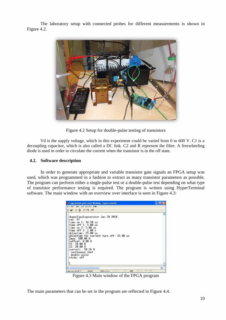
The laboratory setup with connected probes for different measurements is shown in
Figure 4.2.
Figure 4.2 Setup for double-pulse testing of transistors
Vd is the supply voltage, which in this experiment could be varied from 0 to 600 V. C1 is a
decoupling capacitor, which is also called a DC link. C2 and R represent the filter. A freewheeling
diode is used in order to circulate the current when the transistor is in the off state.
4.2. Software description
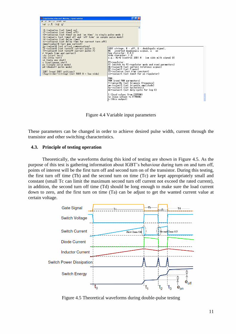
In order to generate appropriate and variable transistor gate signals an FPGA setup was
used, which was programmed in a fashion to extract as many transistor parameters as possible.
The program can perform either a single-pulse test or a double-pulse test depending on what type
of transistor performance testing is required. The program is written using HyperTerminal
software. The main window with an overview over interface is seen in Figure 4.3:
Figure 4.3 Main window of the FPGA program
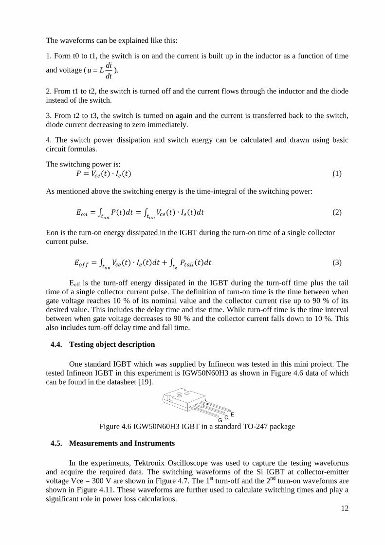
The main parameters that can be set in the program are reflected in Figure 4.4.
11
Figure 4.4 Variable input parameters
These parameters can be changed in order to achieve desired pulse width, current through the
transistor and other switching characteristics.
4.3. Principle of testing operation
Theoretically, the waveforms during this kind of testing are shown in Figure 4.5. As the
purpose of this test is gathering information about IGBT’s behaviour during turn on and turn off,
points of interest will be the first turn off and second turn on of the transistor. During this testing,
the first turn off time (Tb) and the second turn on time (Tc) are kept appropriately small and
constant (small Tc can limit the maximum second turn off current not exceed the rated current),
in addition, the second turn off time (Td) should be long enough to make sure the load current
down to zero, and the first turn on time (Ta) can be adjust to get the wanted current value at
certain voltage.
Figure 4.5 Theoretical waveforms during double-pulse testing
12
The waveforms can be explained like this:
1. Form t0 to t1, the switch is on and the current is built up in the inductor as a function of time
and voltage (di
u Ldt
).
2. From t1 to t2, the switch is turned off and the current flows through the inductor and the diode
instead of the switch.
3. From t2 to t3, the switch is turned on again and the current is transferred back to the switch,
diode current decreasing to zero immediately.
4. The switch power dissipation and switch energy can be calculated and drawn using basic
circuit formulas.
The switching power is:
(1)
As mentioned above the switching energy is the time-integral of the switching power:
(2)
Eon is the turn-on energy dissipated in the IGBT during the turn-on time of a single collector
current pulse.
(3)
Eoff is the turn-off energy dissipated in the IGBT during the turn-off time plus the tail
time of a single collector current pulse. The definition of turn-on time is the time between when
gate voltage reaches 10 % of its nominal value and the collector current rise up to 90 % of its
desired value. This includes the delay time and rise time. While turn-off time is the time interval
between when gate voltage decreases to 90 % and the collector current falls down to 10 %. This
also includes turn-off delay time and fall time.
4.4. Testing object description
One standard IGBT which was supplied by Infineon was tested in this mini project. The
tested Infineon IGBT in this experiment is IGW50N60H3 as shown in Figure 4.6 data of which
can be found in the datasheet [19].
Figure 4.6 IGW50N60H3 IGBT in a standard TO-247 package
4.5. Measurements and Instruments
In the experiments, Tektronix Oscilloscope was used to capture the testing waveforms
and acquire the required data. The switching waveforms of the Si IGBT at collector-emitter
voltage Vce = 300 V are shown in Figure 4.7. The 1st turn-off and the 2
nd turn-on waveforms are
shown in Figure 4.11. These waveforms are further used to calculate switching times and play a
significant role in power loss calculations.
13
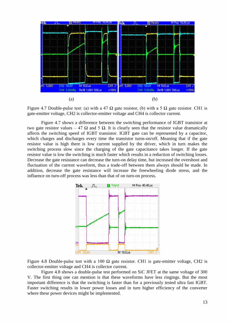
(a) (b)
Figure 4.7 Double-pulse test: (a) with a 47 Ω gate resistor, (b) with a 5 Ω gate resistor. CH1 is
gate-emitter voltage, CH2 is collector-emitter voltage and CH4 is collector current.
Figure 4.7 shows a difference between the switching performance of IGBT transistor at
two gate resistor values – 47 Ω and 5 Ω. It is clearly seen that the resistor value dramatically
affects the switching speed of IGBT transistor. IGBT gate can be represented by a capacitor,
which charges and discharges every time the transistor turns-on/off. Meaning that if the gate
resistor value is high there is low current supplied by the driver, which in turn makes the
switching process slow since the charging of the gate capacitance takes longer. If the gate
resistor value is low the switching is much faster which results in a reduction of switching losses.
Decrease the gate resistance can decrease the turn-on delay time, but increased the overshoot and
fluctuation of the current waveform, thus a trade-off between them always should be made. In
addition, decrease the gate resistance will increase the freewheeling diode stress, and the
influence on turn-off process was less than that of on turn-on process.
Figure 4.8 Double-pulse test with a 100 Ω gate resistor. CH1 is gate-emitter voltage, CH2 is
collector-emitter voltage and CH4 is collector current.
Figure 4.8 shows a double-pulse test performed on SiC JFET at the same voltage of 300
V. The first thing one can mention is that these waveforms have less ringings. But the most
important difference is that the switching is faster than for a previously tested ultra fast IGBT.
Faster switching results in lower power losses and in turn higher efficiency of the converter
where these power devices might be implemented.
14
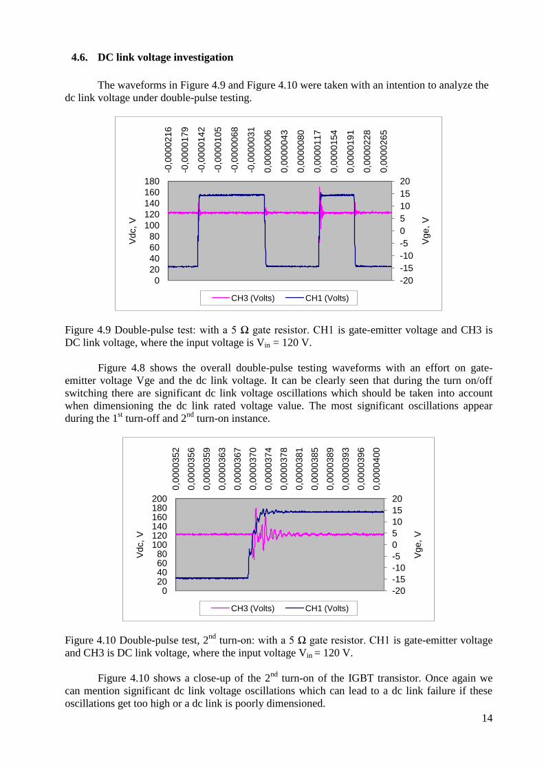
4.6. DC link voltage investigation
The waveforms in Figure 4.9 and Figure 4.10 were taken with an intention to analyze the
dc link voltage under double-pulse testing.
Figure 4.9 Double-pulse test: with a 5 Ω gate resistor. CH1 is gate-emitter voltage and CH3 is
DC link voltage, where the input voltage is Vin = 120 V.
Figure 4.8 shows the overall double-pulse testing waveforms with an effort on gate-
emitter voltage Vge and the dc link voltage. It can be clearly seen that during the turn on/off
switching there are significant dc link voltage oscillations which should be taken into account
when dimensioning the dc link rated voltage value. The most significant oscillations appear
during the 1st turn-off and 2
nd turn-on instance.
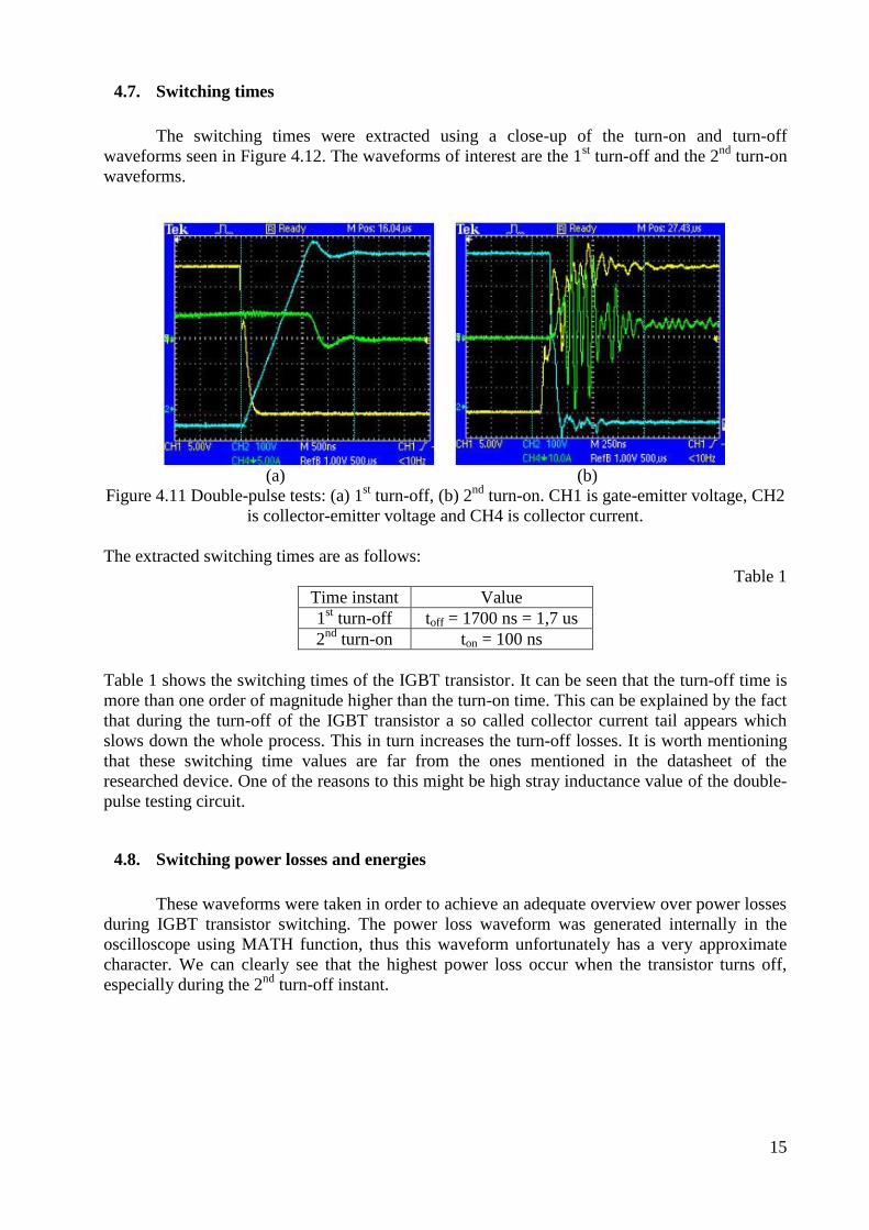
Figure 4.10 Double-pulse test, 2nd
turn-on: with a 5 Ω gate resistor. CH1 is gate-emitter voltage
and CH3 is DC link voltage, where the input voltage Vin = 120 V.
Figure 4.10 shows a close-up of the 2nd
turn-on of the IGBT transistor. Once again we
can mention significant dc link voltage oscillations which can lead to a dc link failure if these
oscillations get too high or a dc link is poorly dimensioned.
-20
-15
-10
-5
0
5
10
15
20
0
20
40
60
80
100
120
140
160
180
-0,0
000216
-0,0
000179
-0,0
000142
-0,0
000105
-0,0
000068
-0,0
000031
0,0
000006
0,0
000043
0,0
000080
0,0
000117
0,0
000154
0,0
000191
0,0
000228
0,0
000265
Vge,
V
Vdc,
V
CH3 (Volts) CH1 (Volts)
-20
-15
-10
-5
0
5
10
15
20
020406080
100120140160180200
0,0
000352
0,0
000356
0,0
000359
0,0
000363
0,0
000367
0,0
000370
0,0
000374
0,0
000378
0,0
000381
0,0
000385
0,0
000389
0,0
000393
0,0
000396
0,0
000400
Vge,
V
Vdc, V
CH3 (Volts) CH1 (Volts)
15
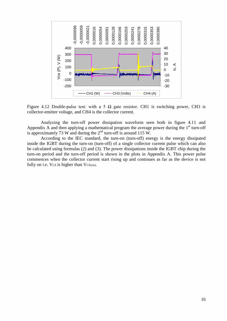
4.7. Switching times
The switching times were extracted using a close-up of the turn-on and turn-off
waveforms seen in Figure 4.12. The waveforms of interest are the 1st turn-off and the 2
nd turn-on
waveforms.
(a) (b)
Figure 4.11 Double-pulse tests: (a) 1st turn-off, (b) 2
nd turn-on. CH1 is gate-emitter voltage, CH2
is collector-emitter voltage and CH4 is collector current.
The extracted switching times are as follows:
Table 1
Time instant Value
1st turn-off toff = 1700 ns = 1,7 us
2nd
turn-on ton = 100 ns
Table 1 shows the switching times of the IGBT transistor. It can be seen that the turn-off time is
more than one order of magnitude higher than the turn-on time. This can be explained by the fact
that during the turn-off of the IGBT transistor a so called collector current tail appears which
slows down the whole process. This in turn increases the turn-off losses. It is worth mentioning
that these switching time values are far from the ones mentioned in the datasheet of the
researched device. One of the reasons to this might be high stray inductance value of the double-
pulse testing circuit.
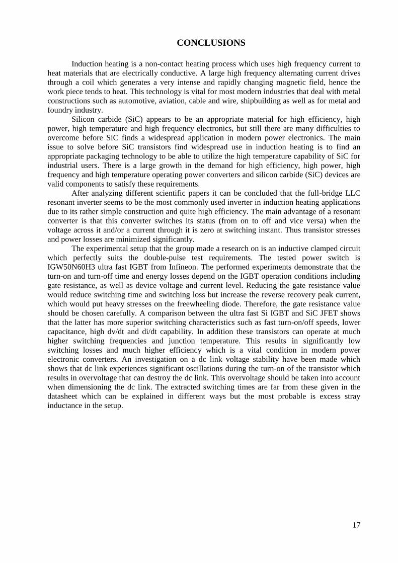
4.8. Switching power losses and energies
These waveforms were taken in order to achieve an adequate overview over power losses
during IGBT transistor switching. The power loss waveform was generated internally in the
oscilloscope using MATH function, thus this waveform unfortunately has a very approximate
character. We can clearly see that the highest power loss occur when the transistor turns off,
especially during the 2nd
turn-off instant.
16
Figure 4.12 Double-pulse test: with a 5 Ω gate resistor. CH1 is switching power, CH3 is
collector-emitter voltage, and CH4 is the collector current.
Analyzing the turn-off power dissipation waveform seen both in figure 4.11 and
Appendix A and then applying a mathematical program the average power during the 1st turn-off
is approximately 73 W and during the 2nd
turn-off is around 115 W.
According to the IEC standard, the turn-on (turn-off) energy is the energy dissipated
inside the IGBT during the turn-on (turn-off) of a single collector current pulse which can also
be calculated using formulas (2) and (3). The power dissipations inside the IGBT chip during the
turn-on period and the turn-off period is shown in the plots in Appendix A. This power pulse
commences when the collector current start rising up and continues as far as the device is not
fully on i.e. VCE is higher than VCE(on).
-30
-20
-10
0
10
20
30
40
-200
-100
0
100
200
300
400
-0,0
000096
-0,0
000059
-0,0
000021
0,0
000016
0,0
000054
0,0
000091
0,0
000128
0,0
000166
0,0
000203
0,0
000241
0,0
000278
0,0
000315
0,0
000353
0,0
000390
Ic, A
Vce (
P),
V (
W)
CH1 (W) CH3 (Volts) CH4 (A)
17
CONCLUSIONS
Induction heating is a non-contact heating process which uses high frequency current to
heat materials that are electrically conductive. A large high frequency alternating current drives
through a coil which generates a very intense and rapidly changing magnetic field, hence the
work piece tends to heat. This technology is vital for most modern industries that deal with metal
constructions such as automotive, aviation, cable and wire, shipbuilding as well as for metal and
foundry industry.
Silicon carbide (SiC) appears to be an appropriate material for high efficiency, high
power, high temperature and high frequency electronics, but still there are many difficulties to
overcome before SiC finds a widespread application in modern power electronics. The main
issue to solve before SiC transistors find widespread use in induction heating is to find an
appropriate packaging technology to be able to utilize the high temperature capability of SiC for
industrial users. There is a large growth in the demand for high efficiency, high power, high
frequency and high temperature operating power converters and silicon carbide (SiC) devices are
valid components to satisfy these requirements.
After analyzing different scientific papers it can be concluded that the full-bridge LLC
resonant inverter seems to be the most commonly used inverter in induction heating applications
due to its rather simple construction and quite high efficiency. The main advantage of a resonant
converter is that this converter switches its status (from on to off and vice versa) when the
voltage across it and/or a current through it is zero at switching instant. Thus transistor stresses
and power losses are minimized significantly.
The experimental setup that the group made a research on is an inductive clamped circuit
which perfectly suits the double-pulse test requirements. The tested power switch is
IGW50N60H3 ultra fast IGBT from Infineon. The performed experiments demonstrate that the
turn-on and turn-off time and energy losses depend on the IGBT operation conditions including
gate resistance, as well as device voltage and current level. Reducing the gate resistance value
would reduce switching time and switching loss but increase the reverse recovery peak current,
which would put heavy stresses on the freewheeling diode. Therefore, the gate resistance value
should be chosen carefully. A comparison between the ultra fast Si IGBT and SiC JFET shows
that the latter has more superior switching characteristics such as fast turn-on/off speeds, lower
capacitance, high dv/dt and di/dt capability. In addition these transistors can operate at much
higher switching frequencies and junction temperature. This results in significantly low
switching losses and much higher efficiency which is a vital condition in modern power
electronic converters. An investigation on a dc link voltage stability have been made which
shows that dc link experiences significant oscillations during the turn-on of the transistor which
results in overvoltage that can destroy the dc link. This overvoltage should be taken into account
when dimensioning the dc link. The extracted switching times are far from these given in the
datasheet which can be explained in different ways but the most probable is excess stray
inductance in the setup.
18
REFERENCES
[1] Bhatnagar, M. and Baliga, B.J., ―Comparison of 6H-SiC, 3C-SiC, and Si for Power Devices,‖
IEEE Transactions on Electron Devices 40(3), 645, 1993.
[2] Neudeck, P.G., Okojie, R.S., and Chen, L.-Y., ―High-Temperature Electronics—A Role for
Wide-Bandgap Semiconductors,‖ Proceedings of the IEEE 90(6), 1065, 2002.
[3] Pierret, R.F., Advanced Semiconductor Fundamentals, Addison-Wesley, Reading, MA, 1987.
[4] Sze, S.M., Physics of Semiconductor Devices, 2nd ed., Wiley-Interscience, New York, 1981.
[5] Baliga, B.J., ―Power Semiconductor Devices for Variable-Frequency Drives,‖ Proceedings of
the IEEE 82(8), 1112, 1994.
[6] Weitzel, C.E., Palmour, J.W., Carter, C.H., Jr., Moore, K., Nordquist, K.J., Allen, S., Thero,
C., and Bhatnagar, M., ―Silicon Carbide High Power Devices,‖ IEEE Transactions on Electron
Devices 43(10), 1732, 1996.
[7] Ozpineci, B., Tolbert, L.M., Islam, S.K., and Hasanuzzaman, M., ―System Impact of Silicon
Carbide Power Devices,‖ International Journal of High Speed Electronics and Systems 12(2),
439, 2002.
[8] Johnson, C.M., ―Comparison of Silicon and Silicon Carbide Semiconductors for a 10 kV
Switching Application,‖ in IEEE 35th Annual Power Electronics Specialists Conference, IEEE,
Piscataway, NJ, 2004, p. 572.
[9] O. Pop and A. Taut, "Analysis and simulation of power inverter with load variation for
Induction heating applications," in Electronics Technology (ISSE), 2010 33rd International
Spring Seminar on, 2010, pp. 378-382.
[10] Tore M. Undeland, Ned Mohan, William P. Robbins, POWER ELECTRONICS: Converters,
Applications and Design 3rd edition: JOHN WILEY &SONS, INC., 2003.
[11] S. Chudjuarjeen, et al., "An Improved LLC Resonant Inverter for Induction Heating
Applications with Asymmetrical Control," Industrial Electronics, IEEE Transactions on, vol.
PP, pp. 1-1, 2010.
[12] Silicon Carbide Technology, Philip G. Neudeck NASA Glenn Research Center, © 2006 by
CRC Press LLC
[13] E. J. Dede, J. Jordán, V. Esteve. "State-of-the Art and Future Trends in Transistorised
Inverters for Induction Heating Applications". ICCDCS 2004. (Punta Cana, Dominican
Republic, Noviembre 2004).
[14] Lorenz, L., ―High Frequency Power Electronic Systems are given by the newest generation
of CoolMOS C3 together with SiC-Schottky diode,‖ PCC-Osaka 2002 Proceeding, April 2-5,
2002, pp. 232-239.
[15] Cree Inc., www.cree.com
[16] SemiSouth Inc., www.semisouth.com
[17] TranSiC AB, www.transic.com
[18] T. L. Skvarenina, Ed., The Power Electronics Handbook (Industrial Electronics). CRC,
2002
[19] www.infineon.com
19
Appendix A
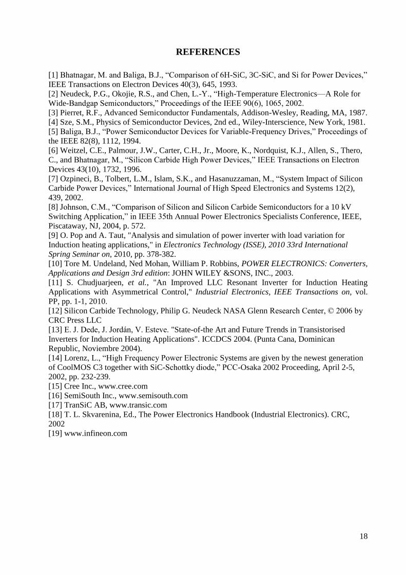
Figure 1 Double-pulse test, 1st turn-off: with a 5 Ω gate resistor. CH1 is switching power, CH3 is
collector-emitter voltage and CH4 is collector current.
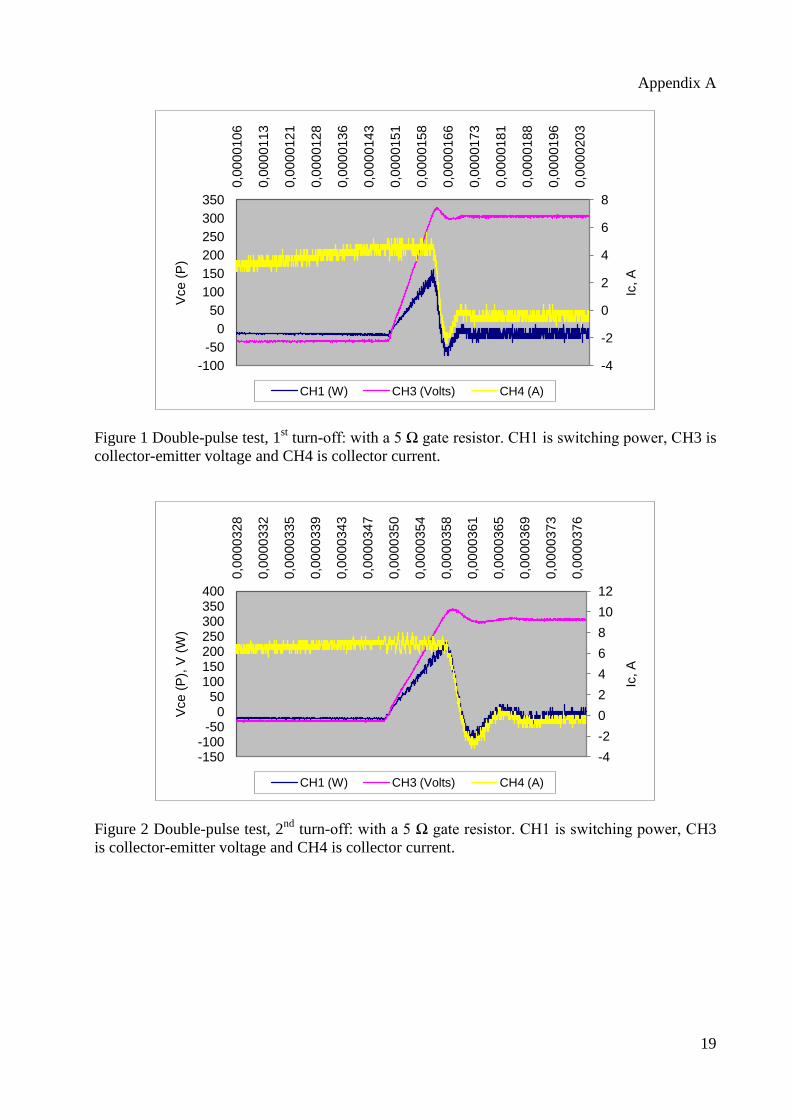
Figure 2 Double-pulse test, 2nd
turn-off: with a 5 Ω gate resistor. CH1 is switching power, CH3
is collector-emitter voltage and CH4 is collector current.
-4
-2
0
2
4
6
8
-100
-50
0
50
100
150
200
250
300
350
0,0
000106
0,0
000113
0,0
000121
0,0
000128
0,0
000136
0,0
000143
0,0
000151
0,0
000158
0,0
000166
0,0
000173
0,0
000181
0,0
000188
0,0
000196
0,0
000203
Ic, A
Vce (
P)
CH1 (W) CH3 (Volts) CH4 (A)
-4
-2
0
2
4
6
8
10
12
-150-100
-500
50100150200250300350400
0,0
000328
0,0
000332
0,0
000335
0,0
000339
0,0
000343
0,0
000347
0,0
000350
0,0
000354
0,0
000358
0,0
000361
0,0
000365
0,0
000369
0,0
000373
0,0
000376
Ic, A
Vce (
P),
V (
W)
CH1 (W) CH3 (Volts) CH4 (A)
20
Appendix B
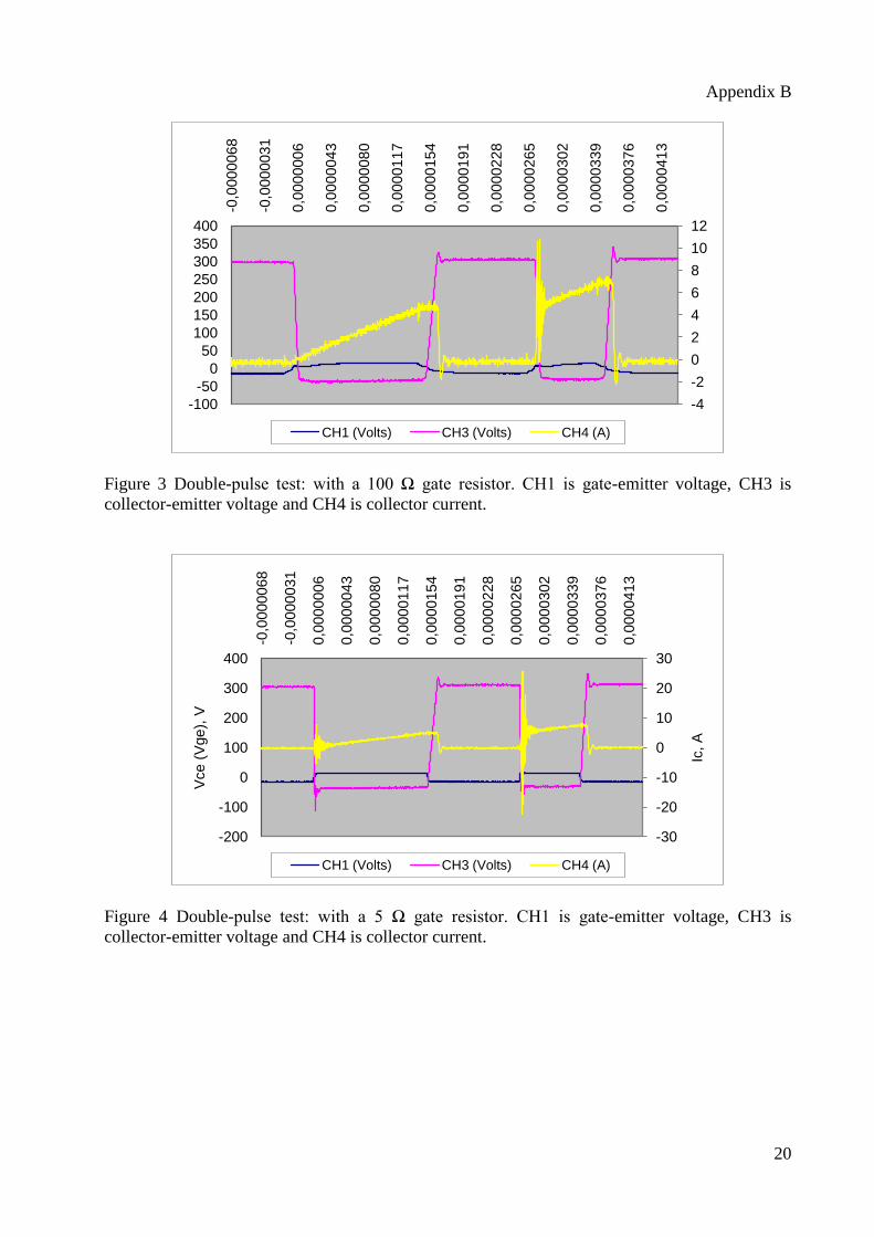
Figure 3 Double-pulse test: with a 100 Ω gate resistor. CH1 is gate-emitter voltage, CH3 is
collector-emitter voltage and CH4 is collector current.
Figure 4 Double-pulse test: with a 5 Ω gate resistor. CH1 is gate-emitter voltage, CH3 is
collector-emitter voltage and CH4 is collector current.
-4
-2
0
2
4
6
8
10
12
-100
-50
0
50
100
150
200
250
300
350
400-0
,0000068
-0,0
000031
0,0
00
00
06
0,0
00
00
43
0,0
00
00
80
0,0
00
01
17
0,0
00
015
4
0,0
00
01
91
0,0
00
02
28
0,0
00
02
65
0,0
00
03
02
0,0
00
03
39
0,0
00
03
76
0,0
00
04
13
CH1 (Volts) CH3 (Volts) CH4 (A)
-30
-20
-10
0
10
20
30
-200
-100
0
100
200
300
400
-0,0
000068
-0,0
000031
0,0
000006
0,0
000043
0,0
000080
0,0
000117
0,0
000154
0,0
000191
0,0
000228
0,0
000265
0,0
000302
0,0
000339
0,0
000376
0,0
000413
Ic, A
Vce (
Vge),
V
CH1 (Volts) CH3 (Volts) CH4 (A)
21
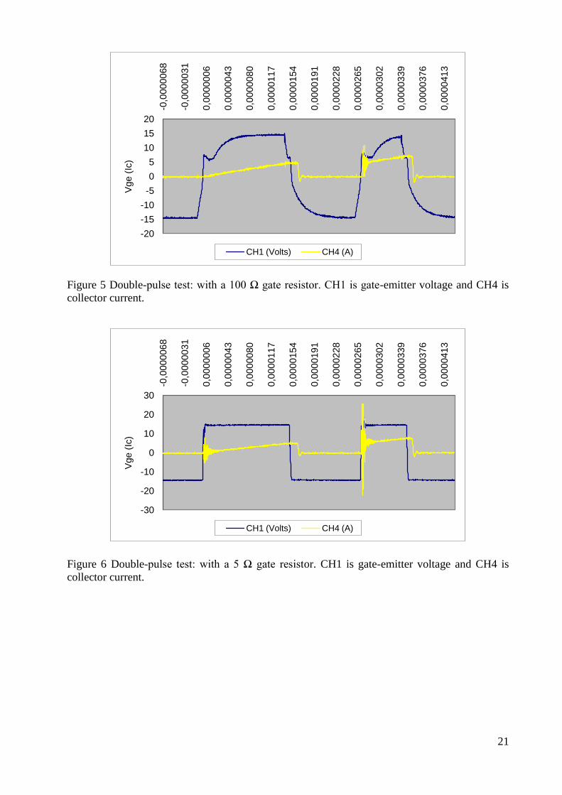
Figure 5 Double-pulse test: with a 100 Ω gate resistor. CH1 is gate-emitter voltage and CH4 is
collector current.
Figure 6 Double-pulse test: with a 5 Ω gate resistor. CH1 is gate-emitter voltage and CH4 is
collector current.
-20
-15
-10
-5
0
5
10
15
20
-0,0
000068
-0,0
000031
0,0
000006
0,0
000043
0,0
000080
0,0
000117
0,0
000154
0,0
000191
0,0
000228
0,0
000265
0,0
000302
0,0
000339
0,0
000376
0,0
000413
Vge (
Ic)
CH1 (Volts) CH4 (A)
-30
-20
-10
0
10
20
30
-0,0
000068
-0,0
000031
0,0
000006
0,0
000043
0,0
000080
0,0
000117
0,0
000154
0,0
000191
0,0
000228
0,0
000265
0,0
000302
0,0
000339
0,0
000376
0,0
000413
Vge (
Ic)
CH1 (Volts) CH4 (A)
22
Appendix C
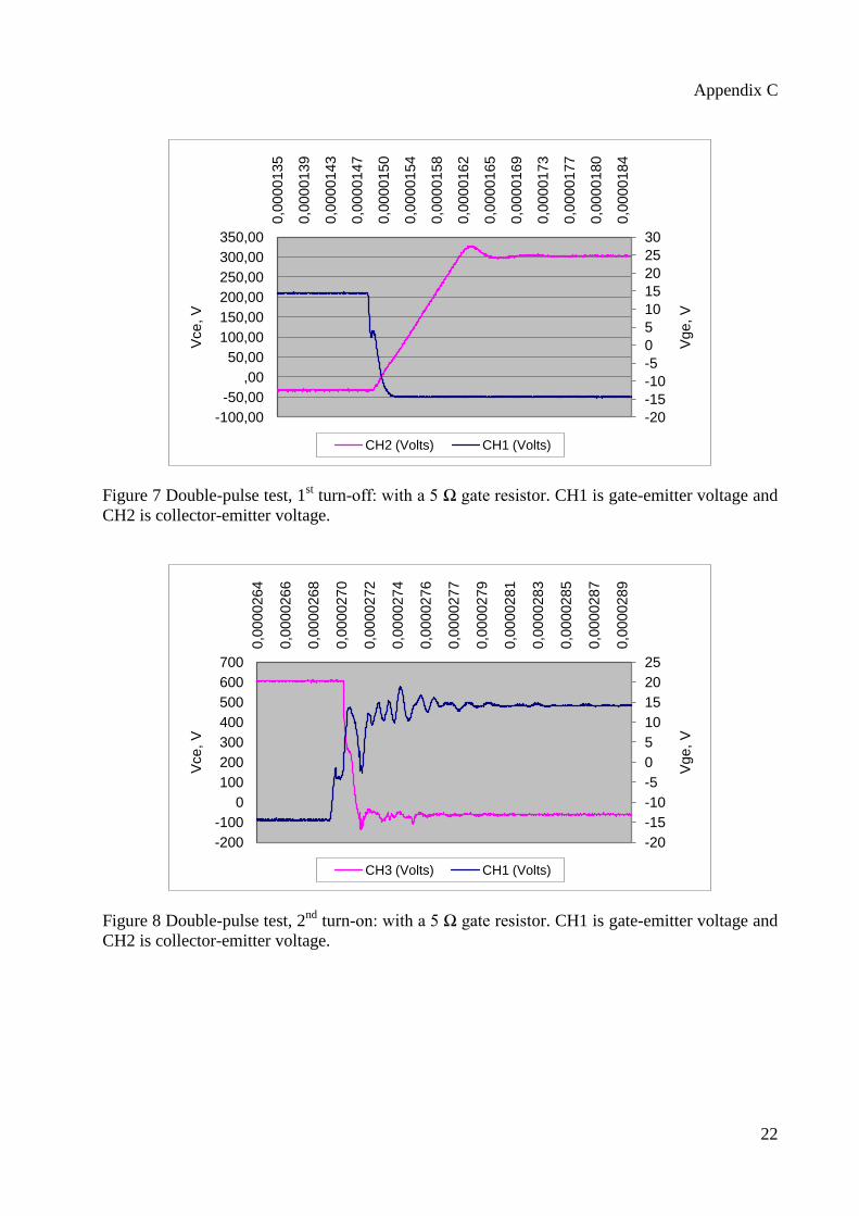
Figure 7 Double-pulse test, 1st turn-off: with a 5 Ω gate resistor. CH1 is gate-emitter voltage and
CH2 is collector-emitter voltage.
Figure 8 Double-pulse test, 2nd
turn-on: with a 5 Ω gate resistor. CH1 is gate-emitter voltage and
CH2 is collector-emitter voltage.
-20
-15
-10
-5
0
5
10
15
20
25
30
-100,00
-50,00
,00
50,00
100,00
150,00
200,00
250,00
300,00
350,00
0,0
000135
0,0
000139
0,0
000143
0,0
000147
0,0
000150
0,0
000154
0,0
000158
0,0
000162
0,0
000165
0,0
000169
0,0
000173
0,0
000177
0,0
000180
0,0
000184
Vge,
V
Vce, V
CH2 (Volts) CH1 (Volts)
-20
-15
-10
-5
0
5
10
15
20
25
-200
-100
0
100
200
300
400
500
600
700
0,0
000264
0,0
000266
0,0
000268
0,0
000270
0,0
000272
0,0
000274
0,0
000276
0,0
000277
0,0
000279
0,0
000281
0,0
000283
0,0
000285
0,0
000287
0,0
000289
Vge,
V
Vce, V
CH3 (Volts) CH1 (Volts)