Embed Size (px)
Citation preview

L. Stevanovic, P. Losee, A. Permuy, G. Dunne, S. Kennerly, S. Arthur, D. Lilienfeld, D. Esler, B. Rowden, J. Nasadoski, M. H. Todorovic, R. Raju, F. Tao, P. Cioffi
GE Global Research, Niskayuna, NY
26 February, 2015
CFES 2015 Annual Conference
Industrial Readiness of SiC Power Devices

2 2/25/2015
Higher max. temperature:
TSiC ≥ 200oC vs. TSi ≤ 175o Reduced power losses…
by more than 50% 2X higher power density… more compact / powerful
More reliable in high temperature environments
Advantages of silicon carbide (SiC) power devices
3 2/25/2015
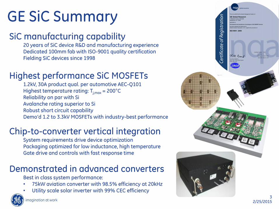
GE SiC Summary SiC manufacturing capability
20 years of SiC device R&D and manufacturing experience Dedicated 100mm fab with ISO-9001 quality certification Fielding SiC devices since 1998
Highest performance SiC MOSFETs 1.2kV, 30A product qual. per automotive AEC-Q101 Highest temperature rating: Tj,max = 200°C Reliability on par with Si Avalanche rating superior to Si Robust short circuit capability Demo’d 1.2 to 3.3kV MOSFETs with industry-best performance
Chip-to-converter vertical integration System requirements drive device optimization Packaging optimized for low inductance, high temperature Gate drive and controls with fast response time
Demonstrated in advanced converters Best in class system performance: • 75kW aviation converter with 98.5% efficiency at 20kHz • Utility scale solar inverter with 99% CEC efficiency

WWW.SUNYIT.EDU WWW.SUNYCNSE.COM
July 15, 2015: NY Governor Andrew M. Cuomo announced that NY State
will launch the NY Power Electronics Manufacturing Consortium
SiC Wafer Fab Located at SUNY Poly campus in Albany:
Class-100 cleanroom with ISO-9001 quality, MES controls and ESD protection
Capacity to produce 30,000-50,000 wafers/year under
New equipment specified for 200mm, capable of processing 150mm wafers
Full complement of metrology and analytical equipment
SUNY Poly’s proven environment for partnership and IP protection
Ramp-up in progress, SiC wafer production will start in late 2016
5 2/25/2015
5 2/25/2015
Industrial Readiness of SiC Devices
Emphasis on cost and reliability – COTS switches have not made significant inroads to date
• Cost challenge will be addressed by the 6” fab
• Rel. challenge: high cost of lost productivity + large number of devices per system
• Important to establish an independent Center for objective evaluation of industrial readiness of candidate SiC components
6 2/25/2015
6 2/25/2015
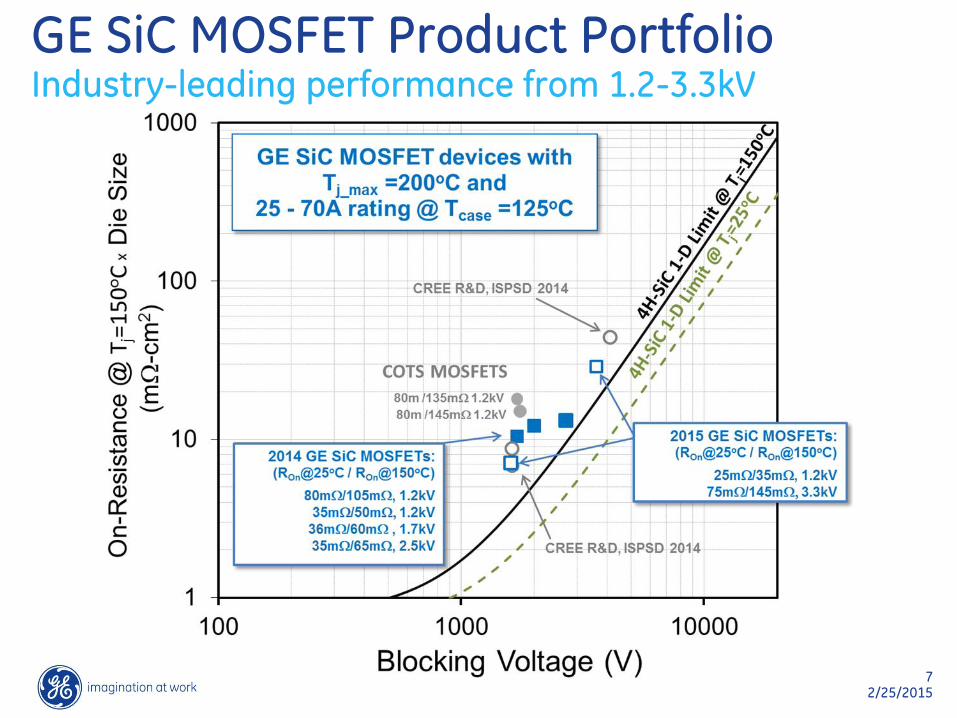
GE SiC MOSFET Product Portfolio
7 2/25/2015
GE SiC MOSFET Product Portfolio Industry-leading performance from 1.2-3.3kV
8 2/25/2015
8 2/25/2015
1.7kV MOSFET Module
9 2/25/2015
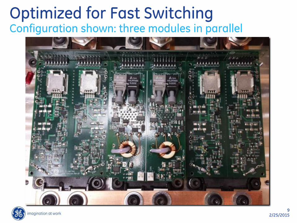
Optimized for Fast Switching Configuration shown: three modules in parallel
10 2/25/2015
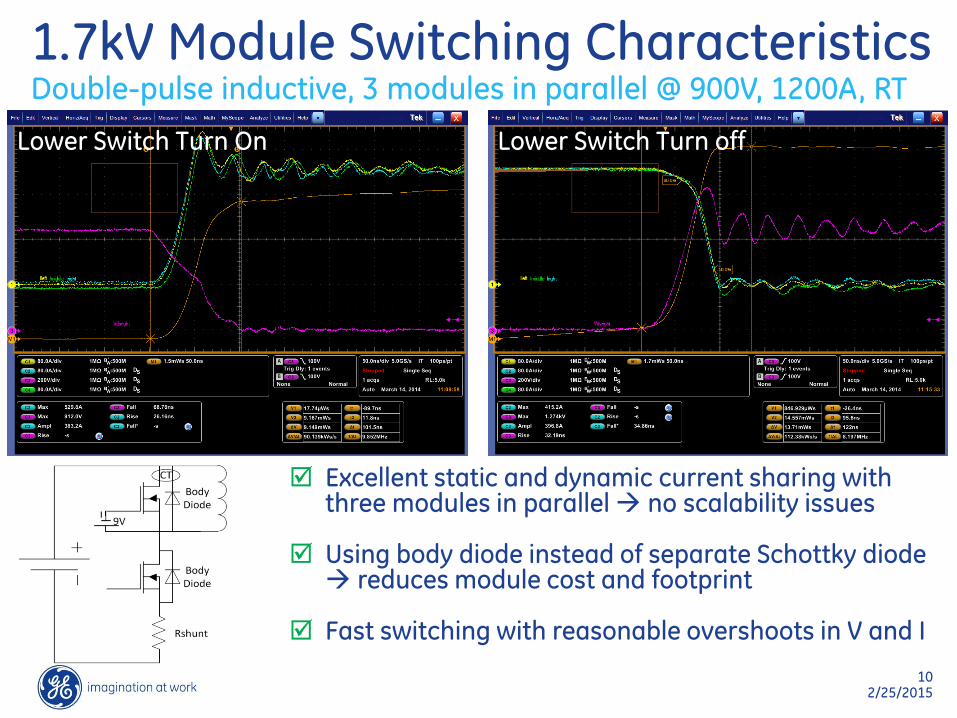
Lower Switch Turn On Lower Switch Turn off
Excellent static and dynamic current sharing with three modules in parallel no scalability issues
Using body diode instead of separate Schottky diode reduces module cost and footprint
Fast switching with reasonable overshoots in V and I
1.7kV Module Switching Characteristics Double-pulse inductive, 3 modules in parallel @ 900V, 1200A, RT
11 2/25/2015
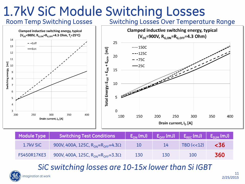
Room Temp Switching Losses Switching Losses Over Temperature Range
SiC switching losses are 10-15x lower than Si IGBT
Module Type Switching Test Conditions EON (mJ) EOFF (mJ) EREC (mJ) ESUM (mJ)
1.7kV SiC 900V, 400A, 125C, RON=ROFF=4.3W 10 14 TBD (<<12) <36
FS450R17KE3 900V, 400A, 125C, RON=ROFF=3.3W 130 130 100 360
1.7kV SiC Module Switching Losses
12 2/25/2015
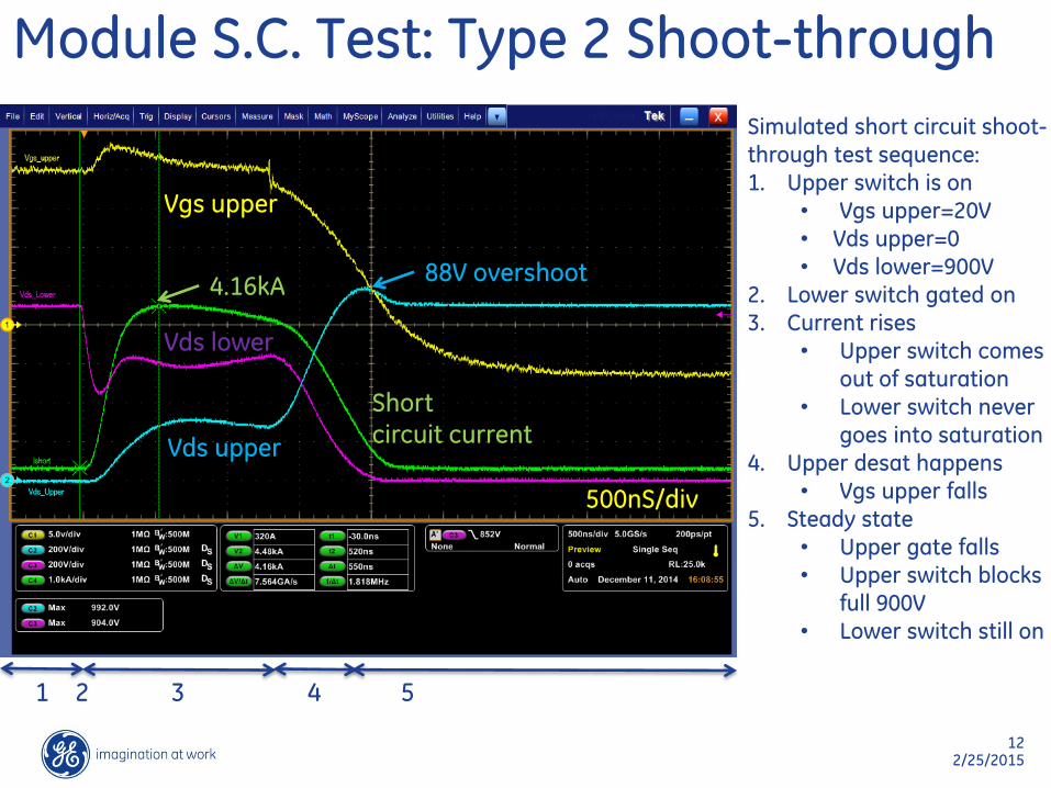
Module S.C. Test: Type 2 Shoot-through
Vgs upper
Vds upper
Vds lower
Short circuit current
4.16kA
Simulated short circuit shoot-
through test sequence:
1. Upper switch is on
• Vgs upper=20V • Vds upper=0
• Vds lower=900V
2. Lower switch gated on
3. Current rises
• Upper switch comes
out of saturation • Lower switch never
goes into saturation
4. Upper desat happens
• Vgs upper falls
5. Steady state
• Upper gate falls • Upper switch blocks
full 900V
• Lower switch still on
500nS/div
1 2 3 4 5
88V overshoot
13 2/25/2015
13 2/25/2015
SiC MOSFET FIT Rate due to Terrestrial Cosmic Radiation (TCR)
14 2/25/2015
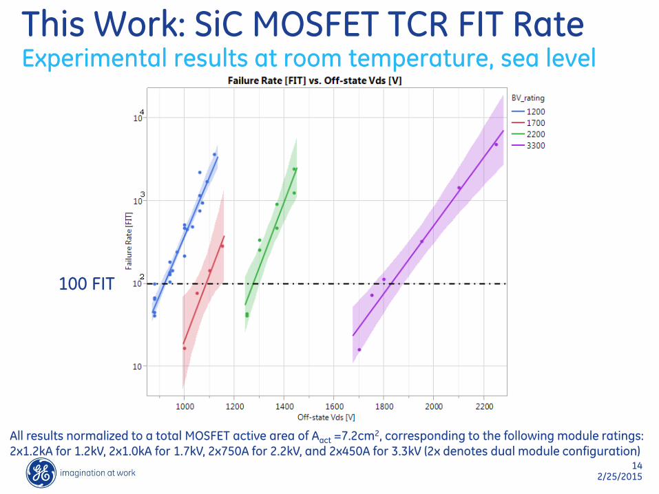
All results normalized to a total MOSFET active area of Aact =7.2cm2, corresponding to the following module ratings: 2x1.2kA for 1.2kV, 2x1.0kA for 1.7kV, 2x750A for 2.2kV, and 2x450A for 3.3kV (2x denotes dual module configuration)
This Work: SiC MOSFET TCR FIT Rate Experimental results at room temperature, sea level
100 FIT

15 2/25/2015
This work: SiC MOSFET TCR-related Voltage Derating to Achieve 100 FIT Higher derating required for high voltage devices
1000 1500 2000 2500 3000 3500
50
55
60
65
70
75
80
VD
S_O
FF/V
DS
_RA
TE
D [
%]
Device rated voltage [V]
Practical off-state voltage to achieve 100 FIT
Summary of the required derating in order to achieve failure rate of 100 FIT for GE SiC MOSFETs.
Having an equivalent active area Aact =7.2cm2, corresponding to the following module ratings:
2x1.2kA for 1.2kV, 2x1.0kA for 1.7kV, 2x750A for 2.2kV, and 2x450A for 3.3kV (2x denotes dual module
configuration). Specifically, in order to provide a failure rate of 100 FIT, only 25% derating is sufficient for the 1200V/1.2kA rated dual module, while the 3.3kV/450A rated module requires 44% derating.
This should be taken into account by system designers utilizing multi-kV rated SiC devices.
A. Bolotnikov, et al. “Overview of 1.2kV – 2.2kV SiC MOSFETs targeted for industrial power conversion applications,” 2015 APEC
16 2/25/2015
16 2/25/2015
MW-scale SiC PV Inverter
17 2/25/2015
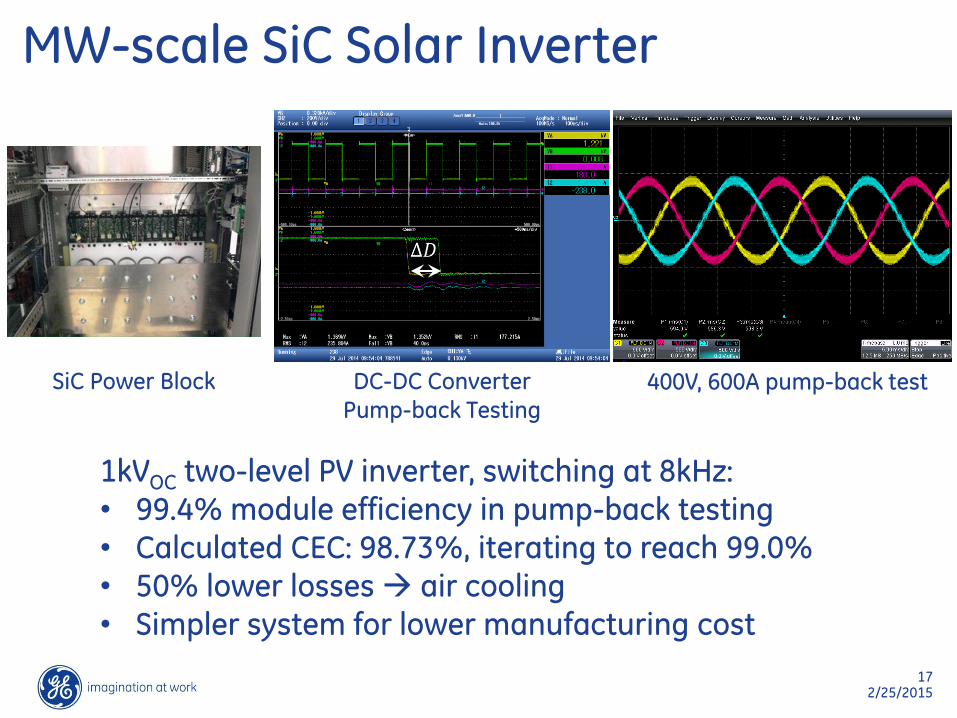
MW-scale SiC Solar Inverter
1kVOC two-level PV inverter, switching at 8kHz: • 99.4% module efficiency in pump-back testing • Calculated CEC: 98.73%, iterating to reach 99.0% • 50% lower losses air cooling • Simpler system for lower manufacturing cost
SiC Power Block DC-DC Converter Pump-back Testing
400V, 600A pump-back test
18 2/25/2015
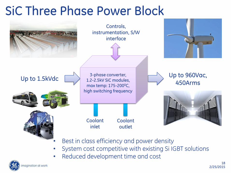
3-phase converter, 1.2-2.5kV SiC modules, max temp: 175-2000C,
high switching frequency
Up to 1.5kVdc Up to 960Vac,
450Arms
Coolant
inlet Coolant
outlet
Controls,
instrumentation, S/W
interface
• Best in class efficiency and power density • System cost competitive with existing Si IGBT solutions • Reduced development time and cost
SiC Three Phase Power Block


20 2/25/2015
20 2/25/2015
SiC MOSFET Reliability
21 2/25/2015
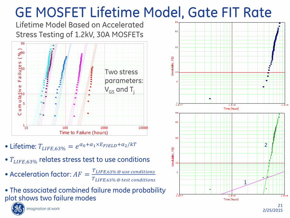
1
2 • Lifetime: 𝑇𝐿𝐼𝐹𝐸,63% = 𝑒𝛼0+𝛼1×𝐸𝐹𝐼𝐸𝐿𝐷+𝛼2/𝑘𝑇
• 𝑇𝐿𝐼𝐹𝐸,63% relates stress test to use conditions
• Acceleration factor: 𝐴𝐹 =𝑇𝐿𝐼𝐹𝐸,63% @ 𝑢𝑠𝑒 𝑐𝑜𝑛𝑑𝑖𝑡𝑖𝑜𝑛𝑠
𝑇𝐿𝐼𝐹𝐸,63% @ 𝑡𝑒𝑠𝑡 𝑐𝑜𝑛𝑑𝑖𝑡𝑖𝑜𝑛𝑠
• The associated combined failure mode probability plot shows two failure modes
Time to Failure (hours)
Cu
mu
lati
ve
Fa
ilu
res (
%)
10 10000100 10001
5
10
50
90
99
Lifetime Model Based on Accelerated Stress Testing of 1.2kV, 30A MOSFETs
GE MOSFET Lifetime Model, Gate FIT Rate
Two stress parameters: VGS and Tj
22 2/25/2015
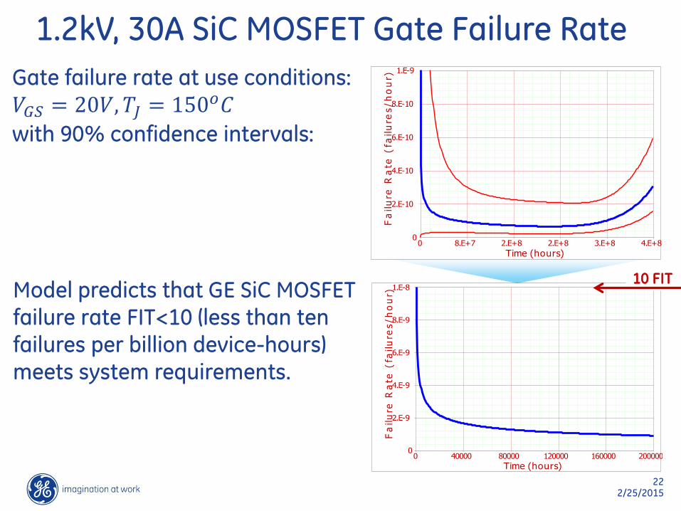
Model predicts that GE SiC MOSFET failure rate FIT<10 (less than ten failures per billion device-hours) meets system requirements.
1.2kV, 30A SiC MOSFET Gate Failure Rate
Gate failure rate at use conditions: 𝑉𝐺𝑆 = 20𝑉, 𝑇𝐽 = 150𝑜𝐶
with 90% confidence intervals:
Time (hours)
Fa
ilu
re R
ate
(fa
ilu
res/h
ou
r)
0 4.E+88.E+7 2.E+8 2.E+8 3.E+80
1.E-9
2.E-10
4.E-10
6.E-10
8.E-10
Time (hours)
Fa
ilu
re R
ate
(fa
ilu
res/h
ou
r)
0 20000040000 80000 120000 1600000
1.E-8
2.E-9
4.E-9
6.E-9
8.E-9
10 FIT
23 2/25/2015
23 2/25/2015
Qualification per Automotive AEC-Q101
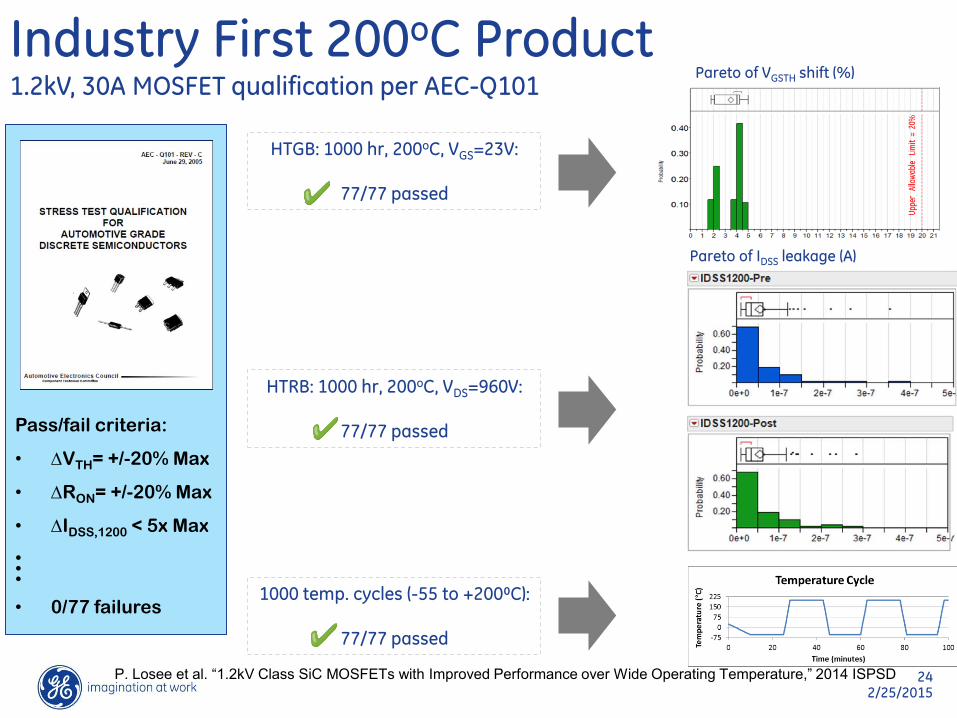
24 2/25/2015
Pass/fail criteria:
• DVTH= +/-20% Max
• DRON= +/-20% Max
• DIDSS,1200 < 5x Max • • •
• 0/77 failures
Industry First 200oC Product 1.2kV, 30A MOSFET qualification per AEC-Q101
Pareto of IDSS leakage (A)
Pareto of VGSTH shift (%)
HTGB: 1000 hr, 200oC, VGS=23V:
77/77 passed
HTRB: 1000 hr, 200oC, VDS=960V:
77/77 passed
1000 temp. cycles (-55 to +200⁰C):
77/77 passed
P. Losee et al. “1.2kV Class SiC MOSFETs with Improved Performance over Wide Operating Temperature,” 2014 ISPSD


![Chapter 2 SiC Materials and Processing Technology€¦ · 34 2 SiC Materials and Processing Technology Table 2.1 Key electrical parameters of SiC [1] Property 4H-SiC 6H-SiC 3C-SiC](https://img.pdfslide.net/doc/110x75/5f4fd11797ddad63bf719816/chapter-2-sic-materials-and-processing-technology-34-2-sic-materials-and-processing.jpg)