Embed Size (px)
Citation preview

Hindawi Publishing CorporationJournal of NanomaterialsVolume 2013 Article ID 561534 7 pageshttpdxdoiorg1011552013561534
Research ArticleInfluence of TiO2 Nanoparticles on Enhancement ofOptoelectronic Properties of PFO-Based Light Emitting Diode
Bandar Ali Al-Asbahi12 Mohammad Hafizuddin Haji Jumali1
Chi Chin Yap1 and Muhamad Mat Salleh3
1 School of Applied Physics Faculty of Science and Technology Universiti Kebangsaan Malaysia (UKM) 43600 BangiSelangor Malaysia
2 Department of Physics Faculty of Science Sanarsquoa University Sanarsquoa Yemen3 Institute of Microengineering and Nanoelectronics (IMEN) Universiti Kebangsaan Malaysia (UKM) 43600 BangiSelangor Malaysia
Correspondence should be addressed to Bandar Ali Al-Asbahi alasbahibandargmailcom andMohammad Hafizuddin Haji Jumali hafizhjukmmy
Received 4 July 2013 Revised 25 September 2013 Accepted 25 September 2013
Academic Editor Yanbao Zhao
Copyright copy 2013 Bandar Ali Al-Asbahi et al This is an open access article distributed under the Creative Commons AttributionLicense which permits unrestricted use distribution and reproduction in any medium provided the original work is properlycited
Improvement on optoelectronic properties of poly (991015840-di-n-octylfluorenyl-27-diyl)- (PFO-) based light emitting diode uponincorporation of TiO
2nanoparticles (NPs) is demonstratedThe PFOTiO
2nanocomposites with different weight ratios between 5
and 35wt were prepared using solution blending method before they were spin coated onto Indium Tin Oxide substrate Then athin Al layer was deposited onto the nanocomposite layer to act as top electrodeThe nanocomposites were tested as emissive layerin organic light emitting diodes (OLEDs) The TiO
2NPs played the most crucial role in facilitating charge transport and electrical
injection and thus improved device performance in terms of turn-on voltage electroluminescence spectra (EL) luminance andluminance efficiency The best composition was OLED with 5wt TiO
2NPs content having moderate surface roughness and
well distribution of NPs The device performance was reduced at higher TiO2NPs content due to higher surface roughness and
agglomeration of TiO2NPsThis work demonstrated the importance of optimum TiO
2NPs content with uniform distribution and
controlled surface roughness of the emissive layer for better device performance
1 Introduction
Organic light emitting diodes (OLEDs) are relatively moreefficient compared to inorganic light emitting diodes sincethey require a relatively small amount of power for the sameamount of light produced Besides that OLEDs offer severalmerits such as easy to fabricate low cost flexible and lowoperating voltage Typical polymers used in organic lightemitting diodes (OLEDs) displays include derivatives of poly(p-phenylene vinylene) (PPV) and polyfluorene (PF) Regret-tably PPV and PF-based light emitting diodes performanceare limited by their poor stability as well as low luminanceefficiency The main reason for the low luminance efficiencyis low electron mobility and high energy barrier between theemissive layer and the electrodes resulted in poor electroninjection Incorporation of inorganic semiconductor which
have low energy barrier to electron injection and high elec-tronmobility into polymer is oneway to resolve the transportand electron injection limitations [1ndash5]
In recent years polymerinorganic nanocompositesreceived much attention from a great number of researchers[6ndash8] This is because the composite systems were reportedto exhibit better thermal mechanical optical and electricalproperties in comparison to the pure polymer Earlier studiessuggested that the suitability and compatibility of any nano-composite materials for optoelectronic applications can bepredicted from detailed study on their fundamental pro-perties in particular conjugated length energy gap andenergy transfer efficiency [9 10] Recently we predicted thesuitability of poly (991015840-di-n-octylfluorenyl-27-diyl) (PFO)TiO2nanocomposite as an emissive layer in OLED devices
[11]
2 Journal of Nanomaterials
The PFO has highest occupied molecular orbital(HOMO) ofminus59 eV and lowest unoccupiedmolecular orbital(LUMO) of minus29 eV [12] while the work function values ofIndium Tin Oxide (ITO) and Al electrodes are minus48 eV andminus43 eV respectively [13] Based on these values the barrierheight between the HOMO of PFO and the ITO is muchsmaller than the barrier height between the LUMO of PFOand the Al electrode (Figure 1) Together with poor electronmobility compared to hole mobility in PFO huge barrierheight between the LUMO of PFO and the Al electroderesulted in the notorious charge imbalance problem in PFOInsertion of suitable entity into PFO matrix to form a smallbarrier height for electron injection is thought as the bestsolution for this problem
This work investigated the effect of TiO2NPs contents
(valence band and conduction band of minus74 eV and minus42 eVresp [14]) embedded into PFO on the formation of a smallerbarrier height for electron injection at PFOAl interface Inaddition this work reports the effect of TiO
2NPs content
on performance of the PFO-based OLED in terms of turn-on voltage electroluminescence spectra (EL) luminanceand luminance efficiency The Commision International deIrsquoEclairage (CIE) chromaticity diagram was used to map thecolors of theOLEDdevices Finally the effect of the filmmor-phology on the device performance was demonstrated
2 Experimental Procedures
21 Materials The poly (991015840-di-n-octylfluorenyl-27-diyl)(PFO) (Mw = 58200) and TiO
2powder (mean size of
25 nm) were purchased from Sigma Aldrich USA Thesematerials were stored in the dry box and used without furtherpurification All materials were dissolved in toluene solventproduced by Fluka ITO coated glass substrate with a sheetresistance of 50Ωsq was purchased fromMerck Balzers andused in this study
22 Samples Preparation and OLED Fabrication As pre-viously reported [11] the solution blending method wasemployed for the preparation of PFOTiO
2nanocomposites
TiO2NPs with different weight ratios (5 15 25 and 35wt)
were added into fixed concentration of PFO (15mgmL)Themixtures were stirred at 600 rpm overnight followed by son-ication for 1 h to get homogeneous nanocomposite solutions
Prior to OLED fabrications the ITO which served asanode was firstly etched and patterned by exposing to thevapor of nitric acid (HNO
3) and hydrochloric acid (HCl) in a
molar ratio of 3 1 Next the ITO was cleaned sequentially inisopropanol and acetone under ultrasonication for 10minuteseach to clean the surface and remove any impurities
Using spin coating technique 100 120583L of PFOTiO2nano-
composite solution was deposited onto a substrate withdimensions of 12 cm times 2 cm to form a thin layer The deposi-tion parameterswere fixed at 2000 rpm for 30 secThen it wasbaked at 120∘C for 10minutes in a vacuumoven to remove thesolvent from the film A thin aluminum layer on the nano-composite film was deposited using electron beam chamber
Vacuum
Vacuum
ITO
Al
Vacuum
43 eV
48 eV
29 eV
74 eV
42 eV
59 eV
Refer to HOMO and LUMO of PFORefer to vibronic band and conducting band of TiO2 NPs
Figure 1 Energy band diagram for AlPFOTiO2ITOOLEDdevice
relative to vacuum
with deposition rate of 2 Amin at the chamber pressure of 25times 10minus6 Pa
23 Samples Characterization The current density-voltage(J-V) was obtained using a Keithley 238measurement systemwhereas electroluminescence spectra (EL) luminance andcolor measurements were obtained using HR2000 OceanOptic Spectrometer The values of turn-on voltage for alldevices are defined as the voltage at the device luminance of05 cdm2 The surface morphology of the films was investi-gated by Scanning ProbeMicroscope (SPM) in tappingmodeusing phosphorous doped Si probe (modelVeecoCONT20A-CP part no MPP-31123-10)
3 Results and Discussion
31 Current Density-Voltage Measurements The currentdensity-voltage (J-V) characteristics of the pristine PFO andPFOTiO
2nanocomposites OLED devices are shown in Fig-
ure 2 Continuous reduction in turn-on voltage of injec-tion current was observed in the PFOTiO
2nanocomposite
devices as compared to the pure PFO (Table 1)These positivefindings can be understood as better injection of chargecarrier resulted from lower potential barrier at the nanocom-posite-electrode interface [15] On the other hand the risingof current density with the TiO
2NPs content may possibly
attributed to reduction in both the resistance and activationenergy of the PFOTiO
2layer which facilitated charge trans-
port [1 12]
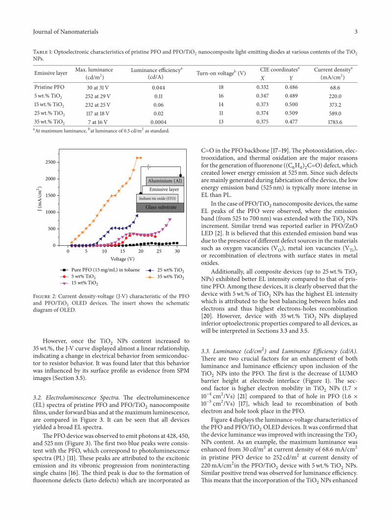
Journal of Nanomaterials 3
Table 1 Optoelectronic characteristics of pristine PFO and PFOTiO2 nanocomposite light-emitting diodes at various contents of the TiO2NPs
Emissive layer Max luminance(cdm2)
Luminance efficiencya(cdA) Turn-on voltageb (V) CIE coordinatesa Current densitya
(mAcm2)119883 119884
Pristine PFO 30 at 31 V 0044 18 0332 0486 6865wt TiO2 252 at 29V 011 16 0347 0489 220015 wt TiO2 232 at 25V 006 14 0373 0500 373225wt TiO2 117 at 18V 002 11 0374 0509 589035wt TiO2 7 at 16V 00004 13 0375 0477 17836aAt maximum luminance bat luminance of 05 cdm2 as standard
0 5 10 15 20 25 300
500
1000
1500
2000
2500
Voltage (V)
Pure PFO (15mgmL) in toluene
J (m
Ac
m2)
Aluminium (Al)Emissive layer
Glass substrate
15 wt TiO2
25 wt TiO2
35 wt TiO25 wt TiO2
Indium tin oxide (ITO)
Figure 2 Current density-voltage (J-V) characteristic of the PFOand PFOTiO
2OLED devices The insert shows the schematic
diagram of OLED
However once the TiO2
NPs content increased to35wt the J-V curve displayed almost a linear relationshipindicating a change in electrical behavior from semiconduc-tor to resistor behavior It was found later that this behaviorwas influenced by its surface profile as evidence from SPMimages (Section 35)
32 Electroluminescence Spectra The electroluminescence(EL) spectra of pristine PFO and PFOTiO
2nanocomposite
films under forward bias and at themaximum luminescenceare compared in Figure 3 It can be seen that all devicesyielded a broad EL spectra
ThePFOdevice was observed to emit photons at 428 450and 525 nm (Figure 3) The first two blue peaks were consis-tent with the PFO which correspond to photoluminescencespectra (PL) [11] These peaks are attributed to the excitonicemission and its vibronic progression from noninteractingsingle chains [16] The third peak is due to the formation offluorenone defects (keto defects) which are incorporated as
C=O in the PFO backbone [17ndash19]The photooxidation elec-trooxidation and thermal oxidation are the major reasonsfor the generation of fluorenone ((C
6H4)2C=O) defect which
created lower energy emission at 525 nm Since such defectsare mainly generated during fabrication of the device the lowenergy emission band (525 nm) is typically more intense inEL than PL
In the case of PFOTiO2nanocomposite devices the same
EL peaks of the PFO were observed where the emissionband (from 525 to 700 nm) was extended with the TiO
2NPs
increment Similar trend was reported earlier in PFOZnOLED [2] It is believed that this extended emission band wasdue to the presence of different defect sources in thematerialssuch as oxygen vacancies (VO) metal ion vacancies (VTi)or recombination of electrons with surface states in metaloxides
Additionally all composite devices (up to 25wt TiO2
NPs) exhibited better EL intensity compared to that of pris-tine PFO Among these devices it is clearly observed that thedevice with 5wt of TiO
2NPs has the highest EL intensity
which is attributed to the best balancing between holes andelectrons and thus highest electrons-holes recombination[20] However device with 35wt TiO
2NPs displayed
inferior optoelectronic properties compared to all devices aswill be interpreted in Sections 33 and 35
33 Luminance (cdcm2) and Luminance Efficiency (cdA)There are two crucial factors for an enhancement of bothluminance and luminance efficiency upon inclusion of theTiO2NPs into the PFO The first is the decrease of LUMO
barrier height at electrode interface (Figure 1) The sec-ond factor is higher electron mobility in TiO
2NPs (17 times
10minus4 cm2Vs) [21] compared to that of hole in PFO (16 times10minus5 cm2Vs) [17] which lead to recombination of bothelectron and hole took place in the PFO
Figure 4 displays the luminance-voltage characteristics ofthe PFO and PFOTiO
2OLED devices It was confirmed that
the device luminance was improved with increasing the TiO2
NPs content As an example the maximum luminance wasenhanced from 30 cdm2 at current density of 686 mAcm2in pristine PFO device to 252 cdm2 at current density of220mAcm2in the PFOTiO
2device with 5wt TiO
2NPs
Similar positive trend was observed for luminance efficiencyThis means that the incorporation of the TiO
2NPs enhanced
4 Journal of Nanomaterials
400 500 600 700 800
002
004
006
008
010
EL (a
u)
500 600 700 8000000
0002
0004
0006
0008
0010
0012
EL (a
u)
525450
428
000
PFO (15mgmL)
120582 (nm)
120582 (nm)
Pure PFO (15mgmL)
15 wt TiO2
5 wt TiO2
25 wt TiO2
35 wt TiO2
Figure 3 EL spectra of PFO and PFOTiO2devices with different
content of TiO2NPs and at applied voltages corresponding to
maximum luminance
the luminance luminance efficiency and current density ofthe PFO device between 250 and 800 This dramaticenhancement was attributed to the incorporation of the TiO
2
NPs which decreased the LUMO barrier height from 14 eVfor PFO to 01 eV at the PFOAl interface as shown in Figure 1In addition at the PFOTiO
2interface the high potential
barrier of electron injection (14 eV) leads to entrapment ofthe electrons in the PFO side before recombination withincoming holes from the ITO (anode) resulted in high lumi-nance The suggested mechanism of these processes is pre-sented in Figure 5(a) It is worth noting that the hole-electronrecombination in the TiO
2side is not allowed which was
evidenced by absence of any peaks in the ultraviolet regionas shown in EL spectra (Figure 3)
Dramatic reduction of luminance and EL intensity wasrecorded once the TiO
2NPs content exceeded 25wt This
could be due to either electrons hopping into the conductionband of the TiO
2or the electrons tunnel through the emissive
layer of the PFOwithout recombining with the holes or com-bination of both as illustrated in Figure 5(b) This electronhopping and tunneling became severe when there is poordistribution of nanoparticles on the emissive layer
34 Color Measurements Figure 6 shows the typical CIEcoordinates of PFO5wt TiO
2OLED device when the
applied voltagewas increased from 18 to 29VThe consistencybetween CIE coordinates and the analysis of EL spectra wasclearly observed This figure displays that a shift was demon-strated with a rise in the applied voltageThe CIE coordinateswere red-shifted from (0319 0487) to (0346 0505) uponrising applied voltage from 18 to 26V After that it shiftedfrom (0346 0503) to (0347 0489) as the applied voltageincreased from 27 to 29V
0 5 10 15 20 25 30 35
0
50
100
150
200
250
Voltage (V)
Lum
inan
ce (c
dm
2)
Pure PFO (15mgmL) 25 wt TiO2
35 wt TiO2
15 wt TiO2
5 wt TiO2
Figure 4 Luminance-voltage characteristics for PFO with variousweight ratios of TiO
2NPs
As summarized in Table 1 a slight shift in CIE coordinatewas demonstrated with the rise of the TiO
2NPs content
at the applied voltage which caused maximum luminanceThis means that the produced color was stable which wasconsistent with EL spectra (Figure 3) As the applied voltageincreased more electrons could be transported across thePFOTiO
2high energy barrier into the LUMO of PFO
and thus the exciton recombination in the PFO side wasincreased On the other hand the CIE coordinates variationwhen the applied voltage increased could be attributed to therise in sensitivity of the electric field during the carrier trans-port and injection [22] The increase in the electric field onboth boundaries of the emitting layer was caused by the rela-tively high voltageMoreover the red-shift inCIE coordinatesas the applied voltage increase is attributed to the extension ofthe recombination zone as well as keto-type defect formation[22]
35 Morphology of PFOTiO2Nanocomposite Films Surface
morphology of pristine PFO and PFOTiO2films in OLED
were observed to play a crucial role in device performanceFigure 7 shows SPM micrographs of PFO and PFOTiO
2
films which were measured over an area of 25 times 25 120583m2Large protuberance formed on the surface of the PFOTiO
2
nanocomposite films as compared to pristine PFO film For-mation of large protuberance was attributed to the agglomer-ation of TiO
2NPs due to strong electrostatic force during the
deposition process [23] This observation was in good agree-ment with the previous report [11]
The root mean square (RMS) roughness exhibited dra-matic increment from 1402 to 7780 nm as shown in Figure 8During deposition the PFO was liquid wetted in the TiO
2
NPs in an effect known as capillarity which consequentlyincreased the surface roughness This induced roughness at
Journal of Nanomaterials 5
ITOAl
PFO TiO2
(a)
Hopping
ITO Al
PFO
Tunneling
TiO2
(b)
Figure 5 Mechanism of (a) charge injectiontransport and (b) hopping and tunneling of electrons in the OLED device (Open circle holeclosed circle electron) A pair of hole and electron indicates an exciton
00 01 02 03 04 05 06 07 0800
02
04
06
08
10
490
480
470
620600
580
560
540
520
CIE Y
CIE X
Figure 6 CIE coordinates of PFOTiO2OLED devices when the
applied voltage was increased from 18 to 29V
the interface between the Al cathode and the PFOTiO2layer
which assisted electron injection [1]As shown in Table 1 it can be seen that the device at
5 wt TiO2NPs exhibited significantly better optoelectronic
properties compared to other devices Despite similar rough-ness with pristine PFO device the superior optoelectronicproperties of this device suggest the importance of TiO
2NPs
in the nanocomposite system compared to roughnessAs TiO
2NP contents increased the devices continued to
exhibit reduction in turn-on voltage a direct consequence ofincrement in roughness [1] Unfortunately this reductionwasat the expense of luminance and luminance efficiency Forexample at 15 wt TiO
2NPs content the luminance and
luminance efficiency were dropped by 8 and 45 respec-tively compared to the same parameters for device with5wt TiO
2NPs content As the TiO
2NPs content increased
to 25wt the luminance was halved from the highest value
while luminance efficiency was significantly inferior even ifcompared to pristine PFOThe huge reduction in both prop-erties was contributed by the gigantic increment in surfaceroughness attributed to the presence of large amount of TiO
2
NPsA more dramatic reduction can be observed in device
with 35wt TiO2NPs content in which the presence
of large protuberance although produce similar roughnesswith 25wt TiO
2NPs resulted in the material to lose
its semiconducting behavior as demonstrated in Figure 1Due to severe agglomeration this nanocomposite behavedas matrix material which reduced the interface betweenPFO and TiO
2NPs and hence significantly reduced charge
transport Similar observation has been reported byMadhaveRao and coworkers in a 23-dibutoxy-14-poly (phenylenevinylene) (DBPPV)ZnO nanocomposite at high content ofZnO NRs [1] Additional evidence of severe agglomerationin the PFO TiO
2nanocomposites system has been demon-
strated by FE-SEM images [11]
4 Conclusion
The solution blending method was successfully used to pre-pare PFOTiO
2nanocomposites whichwere used as emissive
layer in OLED devices The optoelectronic properties ofthe devices were strongly influenced by the TiO
2weight
fraction Based on the current work the device with 5wtof TiO
2NPs exhibited the best performance contributed by
optimumbalance between holes and electrons recombinationas well as good surface roughness In contrast the device with35wt displayed the worst performance attributed mainlyto extremely high surface roughness and agglomeration Thered-shift of CIE coordinates which related to maximumluminance upon addition of TiO
2NPs illustrating the exten-
sion of the recombination zone for holes and electrons inthe OLED devices The current work showed that carefullycontrol TiO
2NPs content in the starting composition is cru-
cial to achieve optimum balance for excitons recombination
6 Journal of Nanomaterials
40n
md
iv
000 100 200(120583m)
(120583mdiv)
(120583m
div)
(120583mdiv)
000520
050
050
(120583mdiv)
(120583m
div)
(120583mdiv)
000820
050
050
40n
md
iv
000 100 200(120583m)
(120583mdiv)
(120583m
div)
(120583mdiv)
0
050
050
0013
(120583mdiv)
(120583m
div)
(120583mdiv)
0
050
050
030
(120583m
div)
(120583mdiv)
050
050
(120583mdiv)
00 19
000 100 200(120583m)
100
nmd
iv
000 100 200(120583m)
000 100 200(120583m)
010
120583m
div
010
120583m
div
Figure 7 2D and 3D SPM images of PFO and PFOTiO2nanocomposites measured over an area of 25 times 25 120583m2
Journal of Nanomaterials 7
0 5 10 15 20 25 30 35 40
0
20
40
60
80
100
RMS
roug
hnes
s (nm
)
TiO2 content (wt)
Figure 8 Root mean square (RMS) roughness for PFOTiO2films
as a function of TiO2NPs content
and suitable for the surface roughness for better devicesperformance
Acknowledgment
The authors would like to thank the Universiti KebangsaanMalaysia (UKM) for providing excellent research facilitiesunder the Research University Grants DPP-2013-048 andDLP-2013-012
References
[1] M V Madhava Rao Y K Su T S Huang C-H Yeh andM-LTu ldquoElectroluminescent characteristics of DBPPV-ZnO nano-composite polymer light emitting devicesrdquo Nanoscale ResearchLetters vol 4 no 5 pp 485ndash490 2009
[2] M Willander O Nur S Zaman A Zainelabdin N Bano andI Hussain ldquoZinc oxide nanorodspolymer hybrid heterojunc-tions for white light emitting diodesrdquo Journal of Physics D vol44 no 22 Article ID 224017 2011
[3] MCocchi J Kalinowski DVirgili and J AGWilliams ldquoExci-mer-based rednear-infrared organic light-emitting diodeswithvery high quantum efficiencyrdquo Applied Physics Letters vol 92no 11 Article ID 113302 2008
[4] M C Suh H K Chung S-Y Kim J H Kwon and B D ChinldquoCathode diffusion and degradation mechanism of polymericlight emitting devicesrdquo Chemical Physics Letters vol 413 no 1ndash3 pp 205ndash209 2005
[5] H Yang and P H Holloway ldquoElectroluminescence from hybridconjugated polymer-CdsMnZnS coreshell nanocrystals devi-cesrdquo Journal of Physical Chemistry B vol 107 no 36 pp 9705ndash9710 2003
[6] M J Tommalieh and A M Zihlif ldquoOptical properties of poly-imidesilica nanocompositerdquo Physica B Condensed Matter vol405 no 23 pp 4750ndash4754 2010
[7] A Kongsinlark G L Rempel and P Prasassarakich ldquoSynthesisof monodispersed polyisoprene-silica nanoparticles via differ-ential microemulsion polymerization and mechanical proper-ties of polyisoprene nanocompositerdquo Chemical EngineeringJournal vol 193-194 pp 215ndash226 2012
[8] J Rozra I Saini A Sharma et al ldquoCu nanoparticles inducedstructural optical and electrical modification in PVArdquo Materi-als Chemistry and Physics 2012
[9] E Dovgolevsky S Kirmayer E Lakin Y Yang C J Brinker andG L Frey ldquoSelf-assembled conjugated polymer-surfactant-sil-icamesostructures and their integration into light-emitting dio-desrdquo Journal of Materials Chemistry vol 18 no 4 pp 423ndash4362008
[10] A Cirpan L Ding and F E Karasz ldquoOptical and electrolu-minescent properties of polyfluorene copolymers and theirblendsrdquo Polymer vol 46 no 3 pp 811ndash817 2005
[11] M H H Jumali B A Al-Asbahi C C Yap M M Salleh andM S Alsalhi ldquoOptoelectronic property enhancement of conju-gated polymer in poly (991015840-di-n-octylfluorenyl-27-diyl)titaniananocompositesrdquoThin Solid Films vol 524 pp 257ndash262 2012
[12] M Bajpai R Srivastava M N Kamalasanan R S Tiwari andS Chand ldquoCharge transport and microstructure in PFOMEH-PPV polymer blend thin filmsrdquo Synthetic Metals vol 160 no15-16 pp 1740ndash1744 2010
[13] M Skompska ldquoHybrid conjugated polymersemiconductorphotovoltaic cellsrdquo Synthetic Metals vol 160 no 1-2 pp 1ndash152010
[14] A C Arango S A Carter and P J Brock ldquoCharge transfer inphotovoltaics consisting of interpenetrating networks of conju-gated polymer and TiO
2nanoparticlesrdquo Applied Physics Letters
vol 74 no 12 pp 1698ndash1700 1999[15] AMAssaka P C Rodrigues A RMDeOliveira et al ldquoNovel
fluorine containing polyfluorenes with efficient blue electrolu-minescencerdquo Polymer vol 45 no 21 pp 7071ndash7081 2004
[16] K Sakamoto K Usami Y Uehara and S Ushioda ldquoExcel-lent uniaxial alignment of poly(99-dioctylfluorenyl-27-diyl)induced by photoaligned polyimide filmsrdquo Applied Physics Let-ters vol 87 no 21 Article ID 211910 3 pages 2005
[17] B Arredondo B Romero A Gutierrez-Llorente et al ldquoOn theelectrical degradation and green band formation in 120572- and 120573-phase poly(99-dioctyfluorene) polymer light-emitting diodesrdquoSolid-State Electronics vol 61 no 1 pp 46ndash52 2011
[18] Z Chen and D Ma ldquoImproved color purity and efficiency inpolyfluorene-based light-emitting diodesrdquo Materials Scienceand Engineering B vol 141 no 1-2 pp 71ndash75 2007
[19] X Gong P K Iyer DMoses G C Bazan A J Heeger and S SXiao ldquoStabilized blue emission from polyfluorene-based light-emitting diodes elimination of fluorenone defectsrdquo AdvancedFunctional Materials vol 13 no 4 pp 325ndash330 2003
[20] A P Kulkarni C J Tonzola A Babel and S A Jenekhe ldquoElec-tron transport materials for organic light-emitting diodesrdquoChemistry of Materials vol 16 no 23 pp 4556ndash4573 2004
[21] S H Kim S H Park and K Lee ldquoEfficiency enhancement inpolymer optoelectronic devices by introducing titanium sub-oxide layerrdquo Current Applied Physics vol 10 no 3 pp S528ndashS531 2010
[22] C-H Hsiao S-W Liu C-T Chen and J-H Lee ldquoEmittinglayer thickness dependence of color stability in phosphorescentorganic light-emitting devicesrdquo Organic Electronics vol 11 no9 pp 1500ndash1506 2010
[23] R-H Lee and H-H Lai ldquoEnhancing electroluminescence per-formance ofMEH-PPV based polymer light emitting device viablendingwith organosoluble polyhedral oligomeric silsesquiox-anesrdquo European Polymer Journal vol 43 no 3 pp 715ndash7242007
Submit your manuscripts athttpwwwhindawicom
ScientificaHindawi Publishing Corporationhttpwwwhindawicom Volume 2014
CorrosionInternational Journal of
Hindawi Publishing Corporationhttpwwwhindawicom Volume 2014
Polymer ScienceInternational Journal of
Hindawi Publishing Corporationhttpwwwhindawicom Volume 2014
Hindawi Publishing Corporationhttpwwwhindawicom Volume 2014
CeramicsJournal of
Hindawi Publishing Corporationhttpwwwhindawicom Volume 2014
CompositesJournal of
NanoparticlesJournal of
Hindawi Publishing Corporationhttpwwwhindawicom Volume 2014
Hindawi Publishing Corporationhttpwwwhindawicom Volume 2014
International Journal of
Biomaterials
Hindawi Publishing Corporationhttpwwwhindawicom Volume 2014
NanoscienceJournal of
TextilesHindawi Publishing Corporation httpwwwhindawicom Volume 2014
Journal of
NanotechnologyHindawi Publishing Corporationhttpwwwhindawicom Volume 2014
Journal of
CrystallographyJournal of
Hindawi Publishing Corporationhttpwwwhindawicom Volume 2014
The Scientific World JournalHindawi Publishing Corporation httpwwwhindawicom Volume 2014
Hindawi Publishing Corporationhttpwwwhindawicom Volume 2014
CoatingsJournal of
Advances in
Materials Science and EngineeringHindawi Publishing Corporationhttpwwwhindawicom Volume 2014
Smart Materials Research
Hindawi Publishing Corporationhttpwwwhindawicom Volume 2014
Hindawi Publishing Corporationhttpwwwhindawicom Volume 2014
MetallurgyJournal of
Hindawi Publishing Corporationhttpwwwhindawicom Volume 2014
BioMed Research International
MaterialsJournal of
Hindawi Publishing Corporationhttpwwwhindawicom Volume 2014
Nano
materials
Hindawi Publishing Corporationhttpwwwhindawicom Volume 2014
Journal ofNanomaterials

2 Journal of Nanomaterials
The PFO has highest occupied molecular orbital(HOMO) ofminus59 eV and lowest unoccupiedmolecular orbital(LUMO) of minus29 eV [12] while the work function values ofIndium Tin Oxide (ITO) and Al electrodes are minus48 eV andminus43 eV respectively [13] Based on these values the barrierheight between the HOMO of PFO and the ITO is muchsmaller than the barrier height between the LUMO of PFOand the Al electrode (Figure 1) Together with poor electronmobility compared to hole mobility in PFO huge barrierheight between the LUMO of PFO and the Al electroderesulted in the notorious charge imbalance problem in PFOInsertion of suitable entity into PFO matrix to form a smallbarrier height for electron injection is thought as the bestsolution for this problem
This work investigated the effect of TiO2NPs contents
(valence band and conduction band of minus74 eV and minus42 eVresp [14]) embedded into PFO on the formation of a smallerbarrier height for electron injection at PFOAl interface Inaddition this work reports the effect of TiO
2NPs content
on performance of the PFO-based OLED in terms of turn-on voltage electroluminescence spectra (EL) luminanceand luminance efficiency The Commision International deIrsquoEclairage (CIE) chromaticity diagram was used to map thecolors of theOLEDdevices Finally the effect of the filmmor-phology on the device performance was demonstrated
2 Experimental Procedures
21 Materials The poly (991015840-di-n-octylfluorenyl-27-diyl)(PFO) (Mw = 58200) and TiO
2powder (mean size of
25 nm) were purchased from Sigma Aldrich USA Thesematerials were stored in the dry box and used without furtherpurification All materials were dissolved in toluene solventproduced by Fluka ITO coated glass substrate with a sheetresistance of 50Ωsq was purchased fromMerck Balzers andused in this study
22 Samples Preparation and OLED Fabrication As pre-viously reported [11] the solution blending method wasemployed for the preparation of PFOTiO
2nanocomposites
TiO2NPs with different weight ratios (5 15 25 and 35wt)
were added into fixed concentration of PFO (15mgmL)Themixtures were stirred at 600 rpm overnight followed by son-ication for 1 h to get homogeneous nanocomposite solutions
Prior to OLED fabrications the ITO which served asanode was firstly etched and patterned by exposing to thevapor of nitric acid (HNO
3) and hydrochloric acid (HCl) in a
molar ratio of 3 1 Next the ITO was cleaned sequentially inisopropanol and acetone under ultrasonication for 10minuteseach to clean the surface and remove any impurities
Using spin coating technique 100 120583L of PFOTiO2nano-
composite solution was deposited onto a substrate withdimensions of 12 cm times 2 cm to form a thin layer The deposi-tion parameterswere fixed at 2000 rpm for 30 secThen it wasbaked at 120∘C for 10minutes in a vacuumoven to remove thesolvent from the film A thin aluminum layer on the nano-composite film was deposited using electron beam chamber
Vacuum
Vacuum
ITO
Al
Vacuum
43 eV
48 eV
29 eV
74 eV
42 eV
59 eV
Refer to HOMO and LUMO of PFORefer to vibronic band and conducting band of TiO2 NPs
Figure 1 Energy band diagram for AlPFOTiO2ITOOLEDdevice
relative to vacuum
with deposition rate of 2 Amin at the chamber pressure of 25times 10minus6 Pa
23 Samples Characterization The current density-voltage(J-V) was obtained using a Keithley 238measurement systemwhereas electroluminescence spectra (EL) luminance andcolor measurements were obtained using HR2000 OceanOptic Spectrometer The values of turn-on voltage for alldevices are defined as the voltage at the device luminance of05 cdm2 The surface morphology of the films was investi-gated by Scanning ProbeMicroscope (SPM) in tappingmodeusing phosphorous doped Si probe (modelVeecoCONT20A-CP part no MPP-31123-10)
3 Results and Discussion
31 Current Density-Voltage Measurements The currentdensity-voltage (J-V) characteristics of the pristine PFO andPFOTiO
2nanocomposites OLED devices are shown in Fig-
ure 2 Continuous reduction in turn-on voltage of injec-tion current was observed in the PFOTiO
2nanocomposite
devices as compared to the pure PFO (Table 1)These positivefindings can be understood as better injection of chargecarrier resulted from lower potential barrier at the nanocom-posite-electrode interface [15] On the other hand the risingof current density with the TiO
2NPs content may possibly
attributed to reduction in both the resistance and activationenergy of the PFOTiO
2layer which facilitated charge trans-
port [1 12]
Journal of Nanomaterials 3
Table 1 Optoelectronic characteristics of pristine PFO and PFOTiO2 nanocomposite light-emitting diodes at various contents of the TiO2NPs
Emissive layer Max luminance(cdm2)
Luminance efficiencya(cdA) Turn-on voltageb (V) CIE coordinatesa Current densitya
(mAcm2)119883 119884
Pristine PFO 30 at 31 V 0044 18 0332 0486 6865wt TiO2 252 at 29V 011 16 0347 0489 220015 wt TiO2 232 at 25V 006 14 0373 0500 373225wt TiO2 117 at 18V 002 11 0374 0509 589035wt TiO2 7 at 16V 00004 13 0375 0477 17836aAt maximum luminance bat luminance of 05 cdm2 as standard
0 5 10 15 20 25 300
500
1000
1500
2000
2500
Voltage (V)
Pure PFO (15mgmL) in toluene
J (m
Ac
m2)
Aluminium (Al)Emissive layer
Glass substrate
15 wt TiO2
25 wt TiO2
35 wt TiO25 wt TiO2
Indium tin oxide (ITO)
Figure 2 Current density-voltage (J-V) characteristic of the PFOand PFOTiO
2OLED devices The insert shows the schematic
diagram of OLED
However once the TiO2
NPs content increased to35wt the J-V curve displayed almost a linear relationshipindicating a change in electrical behavior from semiconduc-tor to resistor behavior It was found later that this behaviorwas influenced by its surface profile as evidence from SPMimages (Section 35)
32 Electroluminescence Spectra The electroluminescence(EL) spectra of pristine PFO and PFOTiO
2nanocomposite
films under forward bias and at themaximum luminescenceare compared in Figure 3 It can be seen that all devicesyielded a broad EL spectra
ThePFOdevice was observed to emit photons at 428 450and 525 nm (Figure 3) The first two blue peaks were consis-tent with the PFO which correspond to photoluminescencespectra (PL) [11] These peaks are attributed to the excitonicemission and its vibronic progression from noninteractingsingle chains [16] The third peak is due to the formation offluorenone defects (keto defects) which are incorporated as
C=O in the PFO backbone [17ndash19]The photooxidation elec-trooxidation and thermal oxidation are the major reasonsfor the generation of fluorenone ((C
6H4)2C=O) defect which
created lower energy emission at 525 nm Since such defectsare mainly generated during fabrication of the device the lowenergy emission band (525 nm) is typically more intense inEL than PL
In the case of PFOTiO2nanocomposite devices the same
EL peaks of the PFO were observed where the emissionband (from 525 to 700 nm) was extended with the TiO
2NPs
increment Similar trend was reported earlier in PFOZnOLED [2] It is believed that this extended emission band wasdue to the presence of different defect sources in thematerialssuch as oxygen vacancies (VO) metal ion vacancies (VTi)or recombination of electrons with surface states in metaloxides
Additionally all composite devices (up to 25wt TiO2
NPs) exhibited better EL intensity compared to that of pris-tine PFO Among these devices it is clearly observed that thedevice with 5wt of TiO
2NPs has the highest EL intensity
which is attributed to the best balancing between holes andelectrons and thus highest electrons-holes recombination[20] However device with 35wt TiO
2NPs displayed
inferior optoelectronic properties compared to all devices aswill be interpreted in Sections 33 and 35
33 Luminance (cdcm2) and Luminance Efficiency (cdA)There are two crucial factors for an enhancement of bothluminance and luminance efficiency upon inclusion of theTiO2NPs into the PFO The first is the decrease of LUMO
barrier height at electrode interface (Figure 1) The sec-ond factor is higher electron mobility in TiO
2NPs (17 times
10minus4 cm2Vs) [21] compared to that of hole in PFO (16 times10minus5 cm2Vs) [17] which lead to recombination of bothelectron and hole took place in the PFO
Figure 4 displays the luminance-voltage characteristics ofthe PFO and PFOTiO
2OLED devices It was confirmed that
the device luminance was improved with increasing the TiO2
NPs content As an example the maximum luminance wasenhanced from 30 cdm2 at current density of 686 mAcm2in pristine PFO device to 252 cdm2 at current density of220mAcm2in the PFOTiO
2device with 5wt TiO
2NPs
Similar positive trend was observed for luminance efficiencyThis means that the incorporation of the TiO
2NPs enhanced
4 Journal of Nanomaterials
400 500 600 700 800
002
004
006
008
010
EL (a
u)
500 600 700 8000000
0002
0004
0006
0008
0010
0012
EL (a
u)
525450
428
000
PFO (15mgmL)
120582 (nm)
120582 (nm)
Pure PFO (15mgmL)
15 wt TiO2
5 wt TiO2
25 wt TiO2
35 wt TiO2
Figure 3 EL spectra of PFO and PFOTiO2devices with different
content of TiO2NPs and at applied voltages corresponding to
maximum luminance
the luminance luminance efficiency and current density ofthe PFO device between 250 and 800 This dramaticenhancement was attributed to the incorporation of the TiO
2
NPs which decreased the LUMO barrier height from 14 eVfor PFO to 01 eV at the PFOAl interface as shown in Figure 1In addition at the PFOTiO
2interface the high potential
barrier of electron injection (14 eV) leads to entrapment ofthe electrons in the PFO side before recombination withincoming holes from the ITO (anode) resulted in high lumi-nance The suggested mechanism of these processes is pre-sented in Figure 5(a) It is worth noting that the hole-electronrecombination in the TiO
2side is not allowed which was
evidenced by absence of any peaks in the ultraviolet regionas shown in EL spectra (Figure 3)
Dramatic reduction of luminance and EL intensity wasrecorded once the TiO
2NPs content exceeded 25wt This
could be due to either electrons hopping into the conductionband of the TiO
2or the electrons tunnel through the emissive
layer of the PFOwithout recombining with the holes or com-bination of both as illustrated in Figure 5(b) This electronhopping and tunneling became severe when there is poordistribution of nanoparticles on the emissive layer
34 Color Measurements Figure 6 shows the typical CIEcoordinates of PFO5wt TiO
2OLED device when the
applied voltagewas increased from 18 to 29VThe consistencybetween CIE coordinates and the analysis of EL spectra wasclearly observed This figure displays that a shift was demon-strated with a rise in the applied voltageThe CIE coordinateswere red-shifted from (0319 0487) to (0346 0505) uponrising applied voltage from 18 to 26V After that it shiftedfrom (0346 0503) to (0347 0489) as the applied voltageincreased from 27 to 29V
0 5 10 15 20 25 30 35
0
50
100
150
200
250
Voltage (V)
Lum
inan
ce (c
dm
2)
Pure PFO (15mgmL) 25 wt TiO2
35 wt TiO2
15 wt TiO2
5 wt TiO2
Figure 4 Luminance-voltage characteristics for PFO with variousweight ratios of TiO
2NPs
As summarized in Table 1 a slight shift in CIE coordinatewas demonstrated with the rise of the TiO
2NPs content
at the applied voltage which caused maximum luminanceThis means that the produced color was stable which wasconsistent with EL spectra (Figure 3) As the applied voltageincreased more electrons could be transported across thePFOTiO
2high energy barrier into the LUMO of PFO
and thus the exciton recombination in the PFO side wasincreased On the other hand the CIE coordinates variationwhen the applied voltage increased could be attributed to therise in sensitivity of the electric field during the carrier trans-port and injection [22] The increase in the electric field onboth boundaries of the emitting layer was caused by the rela-tively high voltageMoreover the red-shift inCIE coordinatesas the applied voltage increase is attributed to the extension ofthe recombination zone as well as keto-type defect formation[22]
35 Morphology of PFOTiO2Nanocomposite Films Surface
morphology of pristine PFO and PFOTiO2films in OLED
were observed to play a crucial role in device performanceFigure 7 shows SPM micrographs of PFO and PFOTiO
2
films which were measured over an area of 25 times 25 120583m2Large protuberance formed on the surface of the PFOTiO
2
nanocomposite films as compared to pristine PFO film For-mation of large protuberance was attributed to the agglomer-ation of TiO
2NPs due to strong electrostatic force during the
deposition process [23] This observation was in good agree-ment with the previous report [11]
The root mean square (RMS) roughness exhibited dra-matic increment from 1402 to 7780 nm as shown in Figure 8During deposition the PFO was liquid wetted in the TiO
2
NPs in an effect known as capillarity which consequentlyincreased the surface roughness This induced roughness at
Journal of Nanomaterials 5
ITOAl
PFO TiO2
(a)
Hopping
ITO Al
PFO
Tunneling
TiO2
(b)
Figure 5 Mechanism of (a) charge injectiontransport and (b) hopping and tunneling of electrons in the OLED device (Open circle holeclosed circle electron) A pair of hole and electron indicates an exciton
00 01 02 03 04 05 06 07 0800
02
04
06
08
10
490
480
470
620600
580
560
540
520
CIE Y
CIE X
Figure 6 CIE coordinates of PFOTiO2OLED devices when the
applied voltage was increased from 18 to 29V
the interface between the Al cathode and the PFOTiO2layer
which assisted electron injection [1]As shown in Table 1 it can be seen that the device at
5 wt TiO2NPs exhibited significantly better optoelectronic
properties compared to other devices Despite similar rough-ness with pristine PFO device the superior optoelectronicproperties of this device suggest the importance of TiO
2NPs
in the nanocomposite system compared to roughnessAs TiO
2NP contents increased the devices continued to
exhibit reduction in turn-on voltage a direct consequence ofincrement in roughness [1] Unfortunately this reductionwasat the expense of luminance and luminance efficiency Forexample at 15 wt TiO
2NPs content the luminance and
luminance efficiency were dropped by 8 and 45 respec-tively compared to the same parameters for device with5wt TiO
2NPs content As the TiO
2NPs content increased
to 25wt the luminance was halved from the highest value
while luminance efficiency was significantly inferior even ifcompared to pristine PFOThe huge reduction in both prop-erties was contributed by the gigantic increment in surfaceroughness attributed to the presence of large amount of TiO
2
NPsA more dramatic reduction can be observed in device
with 35wt TiO2NPs content in which the presence
of large protuberance although produce similar roughnesswith 25wt TiO
2NPs resulted in the material to lose
its semiconducting behavior as demonstrated in Figure 1Due to severe agglomeration this nanocomposite behavedas matrix material which reduced the interface betweenPFO and TiO
2NPs and hence significantly reduced charge
transport Similar observation has been reported byMadhaveRao and coworkers in a 23-dibutoxy-14-poly (phenylenevinylene) (DBPPV)ZnO nanocomposite at high content ofZnO NRs [1] Additional evidence of severe agglomerationin the PFO TiO
2nanocomposites system has been demon-
strated by FE-SEM images [11]
4 Conclusion
The solution blending method was successfully used to pre-pare PFOTiO
2nanocomposites whichwere used as emissive
layer in OLED devices The optoelectronic properties ofthe devices were strongly influenced by the TiO
2weight
fraction Based on the current work the device with 5wtof TiO
2NPs exhibited the best performance contributed by
optimumbalance between holes and electrons recombinationas well as good surface roughness In contrast the device with35wt displayed the worst performance attributed mainlyto extremely high surface roughness and agglomeration Thered-shift of CIE coordinates which related to maximumluminance upon addition of TiO
2NPs illustrating the exten-
sion of the recombination zone for holes and electrons inthe OLED devices The current work showed that carefullycontrol TiO
2NPs content in the starting composition is cru-
cial to achieve optimum balance for excitons recombination
6 Journal of Nanomaterials
40n
md
iv
000 100 200(120583m)
(120583mdiv)
(120583m
div)
(120583mdiv)
000520
050
050
(120583mdiv)
(120583m
div)
(120583mdiv)
000820
050
050
40n
md
iv
000 100 200(120583m)
(120583mdiv)
(120583m
div)
(120583mdiv)
0
050
050
0013
(120583mdiv)
(120583m
div)
(120583mdiv)
0
050
050
030
(120583m
div)
(120583mdiv)
050
050
(120583mdiv)
00 19
000 100 200(120583m)
100
nmd
iv
000 100 200(120583m)
000 100 200(120583m)
010
120583m
div
010
120583m
div
Figure 7 2D and 3D SPM images of PFO and PFOTiO2nanocomposites measured over an area of 25 times 25 120583m2
Journal of Nanomaterials 7
0 5 10 15 20 25 30 35 40
0
20
40
60
80
100
RMS
roug
hnes
s (nm
)
TiO2 content (wt)
Figure 8 Root mean square (RMS) roughness for PFOTiO2films
as a function of TiO2NPs content
and suitable for the surface roughness for better devicesperformance
Acknowledgment
The authors would like to thank the Universiti KebangsaanMalaysia (UKM) for providing excellent research facilitiesunder the Research University Grants DPP-2013-048 andDLP-2013-012
References
[1] M V Madhava Rao Y K Su T S Huang C-H Yeh andM-LTu ldquoElectroluminescent characteristics of DBPPV-ZnO nano-composite polymer light emitting devicesrdquo Nanoscale ResearchLetters vol 4 no 5 pp 485ndash490 2009
[2] M Willander O Nur S Zaman A Zainelabdin N Bano andI Hussain ldquoZinc oxide nanorodspolymer hybrid heterojunc-tions for white light emitting diodesrdquo Journal of Physics D vol44 no 22 Article ID 224017 2011
[3] MCocchi J Kalinowski DVirgili and J AGWilliams ldquoExci-mer-based rednear-infrared organic light-emitting diodeswithvery high quantum efficiencyrdquo Applied Physics Letters vol 92no 11 Article ID 113302 2008
[4] M C Suh H K Chung S-Y Kim J H Kwon and B D ChinldquoCathode diffusion and degradation mechanism of polymericlight emitting devicesrdquo Chemical Physics Letters vol 413 no 1ndash3 pp 205ndash209 2005
[5] H Yang and P H Holloway ldquoElectroluminescence from hybridconjugated polymer-CdsMnZnS coreshell nanocrystals devi-cesrdquo Journal of Physical Chemistry B vol 107 no 36 pp 9705ndash9710 2003
[6] M J Tommalieh and A M Zihlif ldquoOptical properties of poly-imidesilica nanocompositerdquo Physica B Condensed Matter vol405 no 23 pp 4750ndash4754 2010
[7] A Kongsinlark G L Rempel and P Prasassarakich ldquoSynthesisof monodispersed polyisoprene-silica nanoparticles via differ-ential microemulsion polymerization and mechanical proper-ties of polyisoprene nanocompositerdquo Chemical EngineeringJournal vol 193-194 pp 215ndash226 2012
[8] J Rozra I Saini A Sharma et al ldquoCu nanoparticles inducedstructural optical and electrical modification in PVArdquo Materi-als Chemistry and Physics 2012
[9] E Dovgolevsky S Kirmayer E Lakin Y Yang C J Brinker andG L Frey ldquoSelf-assembled conjugated polymer-surfactant-sil-icamesostructures and their integration into light-emitting dio-desrdquo Journal of Materials Chemistry vol 18 no 4 pp 423ndash4362008
[10] A Cirpan L Ding and F E Karasz ldquoOptical and electrolu-minescent properties of polyfluorene copolymers and theirblendsrdquo Polymer vol 46 no 3 pp 811ndash817 2005
[11] M H H Jumali B A Al-Asbahi C C Yap M M Salleh andM S Alsalhi ldquoOptoelectronic property enhancement of conju-gated polymer in poly (991015840-di-n-octylfluorenyl-27-diyl)titaniananocompositesrdquoThin Solid Films vol 524 pp 257ndash262 2012
[12] M Bajpai R Srivastava M N Kamalasanan R S Tiwari andS Chand ldquoCharge transport and microstructure in PFOMEH-PPV polymer blend thin filmsrdquo Synthetic Metals vol 160 no15-16 pp 1740ndash1744 2010
[13] M Skompska ldquoHybrid conjugated polymersemiconductorphotovoltaic cellsrdquo Synthetic Metals vol 160 no 1-2 pp 1ndash152010
[14] A C Arango S A Carter and P J Brock ldquoCharge transfer inphotovoltaics consisting of interpenetrating networks of conju-gated polymer and TiO
2nanoparticlesrdquo Applied Physics Letters
vol 74 no 12 pp 1698ndash1700 1999[15] AMAssaka P C Rodrigues A RMDeOliveira et al ldquoNovel
fluorine containing polyfluorenes with efficient blue electrolu-minescencerdquo Polymer vol 45 no 21 pp 7071ndash7081 2004
[16] K Sakamoto K Usami Y Uehara and S Ushioda ldquoExcel-lent uniaxial alignment of poly(99-dioctylfluorenyl-27-diyl)induced by photoaligned polyimide filmsrdquo Applied Physics Let-ters vol 87 no 21 Article ID 211910 3 pages 2005
[17] B Arredondo B Romero A Gutierrez-Llorente et al ldquoOn theelectrical degradation and green band formation in 120572- and 120573-phase poly(99-dioctyfluorene) polymer light-emitting diodesrdquoSolid-State Electronics vol 61 no 1 pp 46ndash52 2011
[18] Z Chen and D Ma ldquoImproved color purity and efficiency inpolyfluorene-based light-emitting diodesrdquo Materials Scienceand Engineering B vol 141 no 1-2 pp 71ndash75 2007
[19] X Gong P K Iyer DMoses G C Bazan A J Heeger and S SXiao ldquoStabilized blue emission from polyfluorene-based light-emitting diodes elimination of fluorenone defectsrdquo AdvancedFunctional Materials vol 13 no 4 pp 325ndash330 2003
[20] A P Kulkarni C J Tonzola A Babel and S A Jenekhe ldquoElec-tron transport materials for organic light-emitting diodesrdquoChemistry of Materials vol 16 no 23 pp 4556ndash4573 2004
[21] S H Kim S H Park and K Lee ldquoEfficiency enhancement inpolymer optoelectronic devices by introducing titanium sub-oxide layerrdquo Current Applied Physics vol 10 no 3 pp S528ndashS531 2010
[22] C-H Hsiao S-W Liu C-T Chen and J-H Lee ldquoEmittinglayer thickness dependence of color stability in phosphorescentorganic light-emitting devicesrdquo Organic Electronics vol 11 no9 pp 1500ndash1506 2010
[23] R-H Lee and H-H Lai ldquoEnhancing electroluminescence per-formance ofMEH-PPV based polymer light emitting device viablendingwith organosoluble polyhedral oligomeric silsesquiox-anesrdquo European Polymer Journal vol 43 no 3 pp 715ndash7242007
Submit your manuscripts athttpwwwhindawicom
ScientificaHindawi Publishing Corporationhttpwwwhindawicom Volume 2014
CorrosionInternational Journal of
Hindawi Publishing Corporationhttpwwwhindawicom Volume 2014
Polymer ScienceInternational Journal of
Hindawi Publishing Corporationhttpwwwhindawicom Volume 2014
Hindawi Publishing Corporationhttpwwwhindawicom Volume 2014
CeramicsJournal of
Hindawi Publishing Corporationhttpwwwhindawicom Volume 2014
CompositesJournal of
NanoparticlesJournal of
Hindawi Publishing Corporationhttpwwwhindawicom Volume 2014
Hindawi Publishing Corporationhttpwwwhindawicom Volume 2014
International Journal of
Biomaterials
Hindawi Publishing Corporationhttpwwwhindawicom Volume 2014
NanoscienceJournal of
TextilesHindawi Publishing Corporation httpwwwhindawicom Volume 2014
Journal of
NanotechnologyHindawi Publishing Corporationhttpwwwhindawicom Volume 2014
Journal of
CrystallographyJournal of
Hindawi Publishing Corporationhttpwwwhindawicom Volume 2014
The Scientific World JournalHindawi Publishing Corporation httpwwwhindawicom Volume 2014
Hindawi Publishing Corporationhttpwwwhindawicom Volume 2014
CoatingsJournal of
Advances in
Materials Science and EngineeringHindawi Publishing Corporationhttpwwwhindawicom Volume 2014
Smart Materials Research
Hindawi Publishing Corporationhttpwwwhindawicom Volume 2014
Hindawi Publishing Corporationhttpwwwhindawicom Volume 2014
MetallurgyJournal of
Hindawi Publishing Corporationhttpwwwhindawicom Volume 2014
BioMed Research International
MaterialsJournal of
Hindawi Publishing Corporationhttpwwwhindawicom Volume 2014
Nano
materials
Hindawi Publishing Corporationhttpwwwhindawicom Volume 2014
Journal ofNanomaterials


![A review of TiO nanoparticles - Home - Springermandescu et al. [17] reported a hydrothermal synthesis of iron and europium codoped TiO 2 materials under mild con-ditions. The photocatalytic](https://img.pdfslide.net/doc/110x75/5e87f78e63b08d63f26d829a/a-review-of-tio-nanoparticles-home-springer-mandescu-et-al-17-reported-a.jpg)