Embed Size (px)
Citation preview

Crosstalk minimization using multiple dielectric substrates
Item Type text; Thesis-Reproduction (electronic)
Authors Valentine, Wendy Leesa, 1964-
Publisher The University of Arizona.
Rights Copyright © is held by the author. Digital access to this materialis made possible by the University Libraries, University of Arizona.Further transmission, reproduction or presentation (such aspublic display or performance) of protected items is prohibitedexcept with permission of the author.
Download date 06/06/2018 09:50:41
Link to Item http://hdl.handle.net/10150/278345
INFORMATION TO USERS
This manuscript has been reproduced from the microfilm master. UMI
films the text directly from the original or copy submitted. Thus, some
thesis and dissertation copies are in typewriter face, while others may
be from any type of computer printer.
The quality of this reproduction is dependent upon the quality of the copy submitted. Broken or indistinct print, colored or poor quality
illustrations and photographs, print bleedthrough, substandard margins,
and improper alignment can adversely affect reproduction.
In the unlikely event that the author did not send UMI a complete
manuscript and there are missing pages, these will be noted. Also, if
unauthorized copyright material had to be removed, a note will indicate
the deletion.
Oversize materials (e.g., maps, drawings, charts) are reproduced by
sectioning the original, beginning at the upper left-hand corner and
continuing from left to right in equal sections with small overlaps. Each
original is also photographed in one exposure and is included in
reduced form at the back of the book.
Photographs included in the original manuscript have been reproduced
xerographically in this copy. Higher quality 6" x 9" black and white
photographic prints are available for any photographs or illustrations
appearing in this copy for an additional charge. Contact UMI directly to order.
University Microfilms International A Bell & Howell Information Company
300 North Zeeb Road. Ann Arbor, Ml 48106-1346 USA 313/761-4700 800/521-0600

Order Number 1353129
Crosstalk minimization using multiple dielectric substrates
Valentine, Wendy Leesa, M.S.
The University of Arizona, 1993
U M I 300 N. Zeeb Rd. Ann Arbor, MI 48106

CROSSTALK MINIMIZATION
USING MULTIPLE DIELECTRIC SUBSTRATES
by
Wendy Leesa Valentine
A Thesis Submitted to the Faculty of the
DEPARTMENT OF ELECTRICAL AND COMPUTER ENGINEERING
In Partial Fulfillment of the Requirements For the Degree of
MASTER OF SCIENCE WITH A MAJOR IN ELECTRICAL ENGINEERING
In the Graduate College
THE UNIVERSITY OF ARIZONA
19 9 3
2
STATEMENT BY AUTHOR
This thesis has been submitted in partial fulfillment of requirements for an advanced degree at The University of Arizona and is deposited in the University Library to be made available to borrowers under rules of the Library.
Brief quotations from this thesis are allowable without special permission, provided that accurate acknowledgment of source is made. Requests for permission for extended quotation from or reproduction of this manuscript in whole or in part may be granted by the head of the major department of the Dean of the Graduate College when in his or her judgement the proposed use of the matrial is in the interests of scholarship. In all other instances, however, permission must be obtained from the author.
SIGNED:
APPROVAL BY THESIS DIRECTOR
This thesis has been approved on the date shown below:
. ^~-v V'? hz Andre^^^Xangellaris Date
Associate Professor of Electrical and Computer Engineering

3
ACKNOWLEDGEMENTS
First and foremost, I would like to thank my advisor, Dr. Andreas
Cangellaris, for his longstanding patience and cooperation in getting
me through this. I would also like to thank Dr. Palusinski and Dr.
Rosenblit for agreeing to be on my committee. For the lessons they
taught me in class and the useful conversations outside of class, I'd
like to thank Dr. Dudley, Dr. J. R. Wait, Dr. Dvorak, and Dr. Gaskill.
I, like every other ECE graduate student, am indebted to Sandi Sledge
for diligently guiding me through the occasionally bewildering maze
of paperwork. I am likewise grateful to the National Consortium for
Graduate Degrees for Minorities in Engineering (GEM) and the
Semiconductor Research Corporation (SRC) for their financial support.
I would like to thank Dean Vern Johnson, Dean Morris Farr, Dean
Glenn Smith, and Dean Adela Allen for their concern and attention.
I'd like to offer a special thanks to David Jarrett who accepted and
encouraged me, even when he thought my brain had gone on
vacation arid to Joseph Wozniak, whose loving concern comforted me
during some of my discouraging moments. To Rob Lee and Diana
Wright who badgered me, counseled me, encouraged me, and skied
with me, thanks. Your efforts and concerns were noticed and
appreciated. I'd also like to thank the unofficial ECE Parchesi Club-
Monica C de Baca, Mike Chan, Mike Pasik, and Chris Spring—for
occasionally letting me sit in on their games. Gene Climer, Sam
Howells, Karen Kolczak, Mary Sepich, Don Wallace, Joy Watanabe, the
Williams Family—you all did much (probably more than you realize)
to enrich my U of A experience.
Finally, I owe an incredible debt to my family. They've tolerated my
moods and quirks since the beginning. Without their love and
support, I would not be who or where I am today. Thankyou.

4
TABLE OF CONTENTS
Page
LIST OF ILLUSTRATIONS 5
ABSTRACT 8
1. INTRODUCTION 9
2. MICROSTRIP LINES AND CROSSTALK 1 0
2.1 Fields 10
2.2 Crosstalk 17
3. RESULTS AND DISCUSSION 2 7
3.1 Software 2 7
3.2 Geometries 3 1
3.3 Family of curves and SPICE simulations 3 3
4. CONCLUSIONS .....6 2
5. REFERENCES 6 5
5
LIST OF ILLUSTRATIONS
Figure Page 2 -1 F ie ld l i nes fo r a s ing le conduc to r i n a homogeneous
medium located over a ground plane 1 0
2 -2 F ie ld l i nes fo r a s ing le mic ros t r ip t r ansmiss ion l i ne 1 1
2 -3 F ie ld l i nes fo r t he even and odd modes fo r a pa i r o f
microstrip transmission lines 1 6
2 -4 In i t i a l impressed vo l t ages on the ac t ive and qu ie t l i nes 19
2 -5 Ef fec t o f even and odd modes hav ing d i f f e ren t ve loc i t i e s 2 0
2 -6 Mic ros t r ip s t ruc tu re 25 2 -7 50MHz s igna l and i t s de r iva t ive , fo=50MHz, t r= t f=1 .0ns , 2 6
3 -1 SPICE mode l fo r t r ansmiss ion l i ne s imula t ions 2 8
3 -2 SPICE mode l fo r n coup led t r ansmiss ion l i nes , [3 ] . . . . . 2 9
3 -3 De ta i l ed mode l fo r t he i t h l i ne [3 ] 3 1
3 -4 S ing le d i e l ec t r i c subs t r a t e geomet ry 3 2
3 -5 Doub le d i e l ec t r i c subs t r a t e geomet ry 3 2
3 -6 Tr ip l e d i e l ec t r i c subs t r a t e geomet ry wi th bu r i ed
conductors 3 3
3 -7 Cra t v s . £ r fo r a s ing le d i e l ec t r i c subs t r a t e w i th conduc to r s
located h=26.0 mils above the ground plane 3 7
3 -8 SPICE p lo t fo r 2 mic ros t r ip l i nes wi th a s ing le d i e l ec t r i c
substrate, £r=3 3 8
3 -9 SPICE p lo t fo r 2 mic ros t r ip l i nes wi th a s ing le d i e l ec t r i c
substrate. Er=10 3 9 3 - 1 0 C r a t v s . E n f o r a d o u b l e d i e l e c t r i c s u b s t r a t e . £ ^ = 1 0 ,
conductors are located h=26.0 mils above the ground
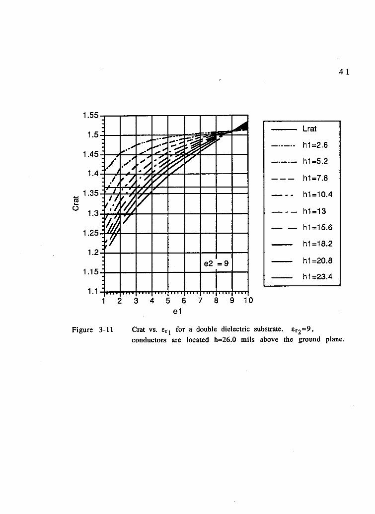
plane 40 3 -11 Crat vs. £rj for a double dielectric substrate. Er2=9 t
conductors are located h=26.0 mils above the ground
plane 4 1
6
LIST OF ILLUSTRATIONS - Continued
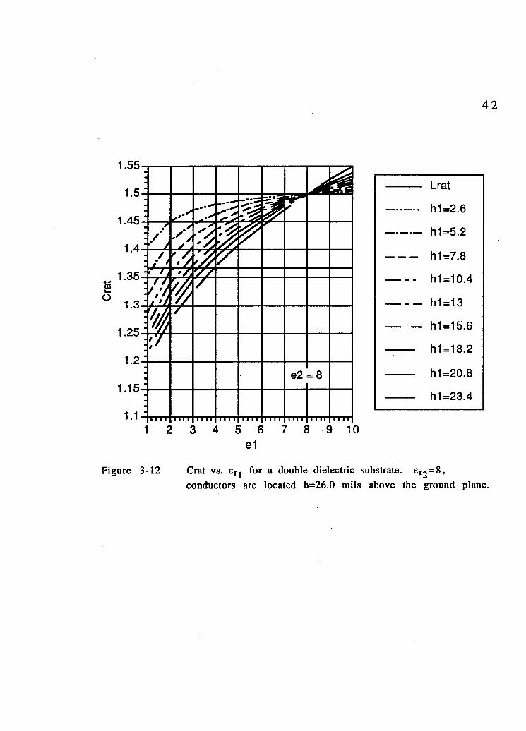
3-12 Crat vs. £ri for a double dielectric substrate. £r2=8,
conductors are located h=26.0 mils above the ground
plane 42 3 -13 SPICE p lo t fo r 2 mic ros t r ip l i nes wi th a doub le d i e l ec t r i c
substrate. £r i=3 , er2=10» hl=10.4 mils 43
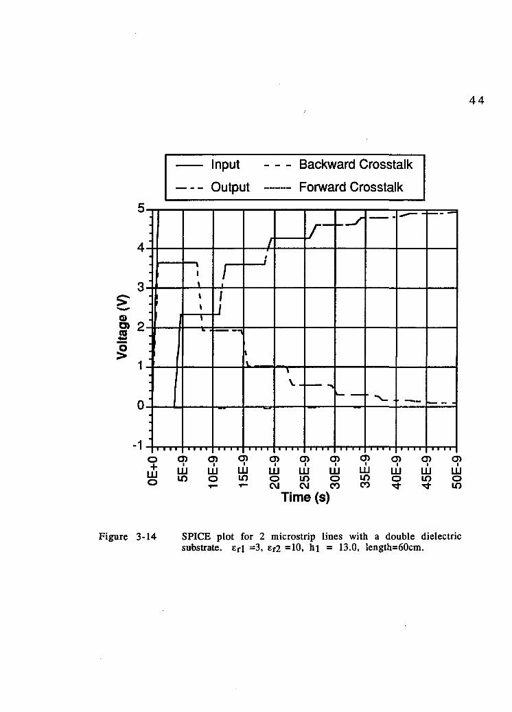
3-14 SPICE p lo t fo r 2 mic ros t r ip l i nes wi th a doub le d i e l ec t r i c substrate. £ri=3, £r2=10, hl=13.0 mils 44
3 -15 SPICE p lo t fo r 2 mic ros t r ip l i nes wi th a doub le d i e l ec t r i c substrate. £r i=3 , £r2=8, hl=15.6 mils 45
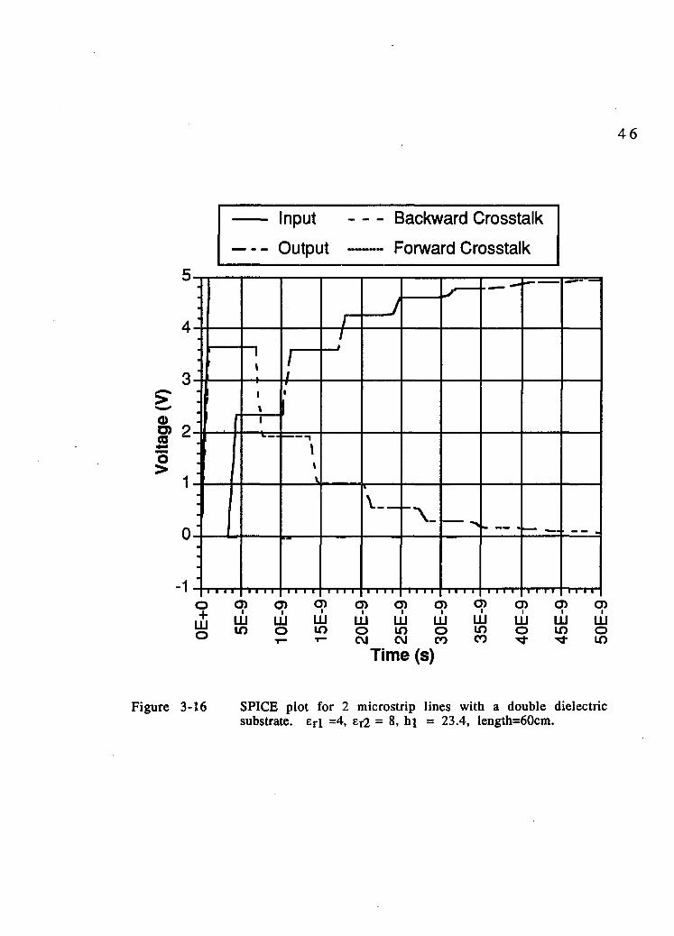
3 -16 SPICE p lo t fo r 2 microstrip lines with a double dielectric substrate. £ri=4, £r2=8, hl=23.4 mils 4 6
3 -17 SPICE p lo t fo r 2 mic ros t r ip l i nes w i th a doub le d i e l ec t r i c substrate. £r i=4, Er2=10, hl=20.8 mils 4 7
3 -18 SPICE p lo t fo r 2 mic ros t r ip l i nes wi th a doub le d i e l ec t r i c substrate. £r i=3, Er2=9> hl=15.6 mils 4 8
3 -19 SPICE p lo t fo r 2 mic ros t r ip l i nes wi th a doub le d i e l ec t r i c substrate. £ri=3, £r2=10» hl=15.6 mils 4 9
3 -20 SPICE p lo t fo r 2 mic ros t r ip l i nes wi th a doub le d i e l ec t r i c substrate. £ri=3, £r2=10» hl=18.2 mils 5 0
3 -21 SPICE p lo t fo r 2 mic ros t r ip l i nes wi th a doub le d i e l ec t r i c substrate. £ri=3, £r2=10, hl=13.0 mils. Active line is
terminated into approximately 2.5Zo. (Figure 3-14 shows
that this case had backward crosstalk when the
terminations were approximately matched.) 5 1
3 -22 SPICE p lo t fo r 2 mic ros t r ip l i nes w i th a doub le d i e l ec t r i c substrate. £ri=3, £r2=10, hl=13.0 mils. Quiet line is
terminated into approximately 2.5Zo on both ends.
(Figure 3-14 shows that this case had backward crosstalk
when the terminations were approximately matched.) 5 2
7
LIST OF ILLUSTRATIONS - Continued
3-23 SPICE p lo t fo r 2 mic ros t r ip l i nes wi th a doub le d i e l ec t r i c substrate. £ri=4, er2=10, hl=20.8 mils. Active line is
terminated into approximately 4Zo. (Figure 3-17 shows
that this case had no backward crosstalk when the
terminations were approximately matched.) 5 3
3 -24 SPICE p lo t fo r 2 mic ros t r ip l i nes wi th a doub le d i e l ec t r i c substrate. £ri=4, er2=10, hl=20.8 mils. Quiet line is
terminated into approximately 4Zo on both ends. (Figure
3-17 shows that this case had no backward crosstalk
when the terminations were approximately matched.) 5 4
3 -25 Tr ip ly coup led t r ansmiss ion l i nes . S igna l i s i npu t t o the
center line 5 5 3 -26 Tr ip ly coup led t r ansmiss ion l i nes . S igna l i s i npu t t o the
end line 6 0
3 -27 SPICE p lo t fo r 3 mic ros t r ip l i nes w i th doub le d i e l ec t r i c substrate. Input and output signals on center line. En—3, er2=10, hl=13.0mils 5 6
3 -28 SPICE p lo t fo r 3 mic ros t r ip l i nes w i th doub le d i e l ec t r i c substrate. Input and output signals on center line. £ri=4,
£12=10, hl=20.8 mils 5 7
3 -29 SPICE p lo t fo r 3 mic ros t r ip l i nes wi th doub le d i e l ec t r i c substrate. Input and output signals on outside line. £r i = 3 ,
£i2=10, hl=13.0 mils 5 8
3 -30 SPICE p lo t fo r 3 mic ros t r ip l i nes wi th doub le d i e l ec t r i c substrate. Input and output signals on outside line. £ri=4,
£,2=10, hl=20.8 mils 5 9
3 -31 Cra t v s . £ r fo r a t r ip l e d i e l ec t r i c subs t r a t e w i th conduc to r s
located h=26.0 mils above the ground plane 6 1
8
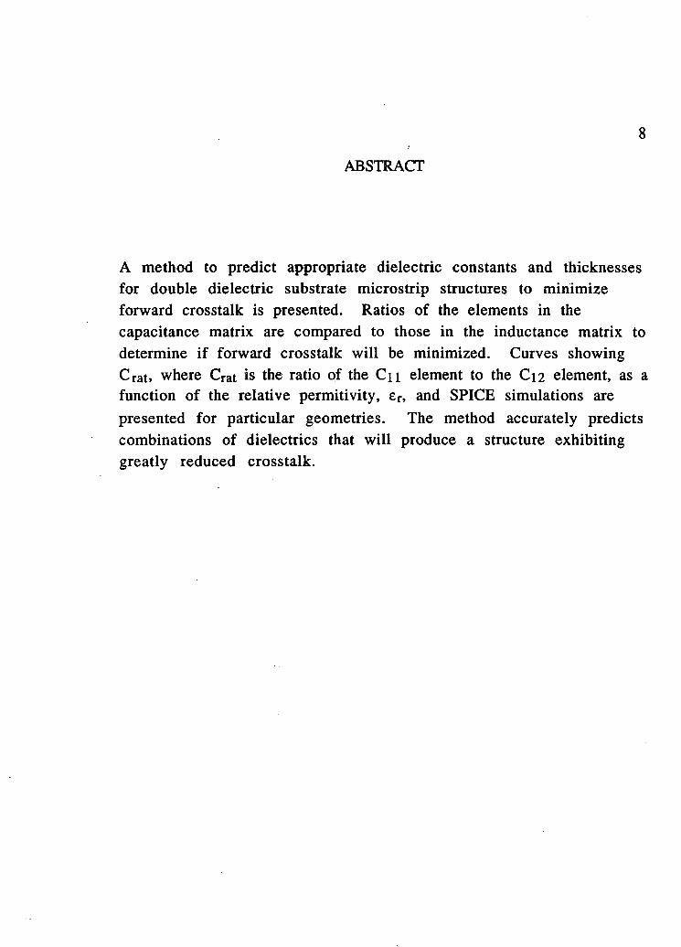
ABSTRACT
A method to predict appropriate dielectric constants and thicknesses
for double dielectric substrate microstrip structures to minimize
forward crosstalk is presented. Ratios of the elements in the
capacitance matrix are compared to those in the inductance matrix to
determine if forward crosstalk will be minimized. Curves showing
Crat, where Crat is the ratio of the Cn element to the C12 element, as a function of the relative permitivity, er, and SPICE simulations are
presented for particular geometries. The method accurately predicts
combinations of dielectrics that will produce a structure exhibiting
greatly reduced crosstalk.
CHAPTER 1
9
INTRODUCTION
As the push for ever faster speeds and smaller devices continues, the
challenge of maintaining signal integrity becomes increasingly
difficult. The issue of crosstalk becomes more important as the circuit densities increase and the noise margins tighten.
Gilb and Balanis [1] showed that forward crosstalk could be
eliminated by using multiple layers of dielectric in the substrate for
a pair of microstrip lines. Forward crosstalk results when the even
and odd modes travel down the microstrip lines at different
velocities. The presence of additional layers in the substrate changes
the velocities of the even and odd modes relative to one another. By
comparing the ratio of the C matrix elements to those of the L matrix
for a given conductor geometry, we can determine which dielectric
geometries will equalize the even and odd mode velocities.
The fields of microstrip lines are briefly discussed in Chapter 2, and a
description of crosstalk in terms of even and odd modes is presented.
Results are presented for various dielectric geometries in Chapter 3.
After a discussion of the software used to produce the data, SPICE
curves depicting the forward and backward crosstalk are presented
for single, double and triple dielectric substrate geometries. Finally,
a brief discussion of the manufacturability of these structures,
conclusions, and recommendations for future work are given in
Chapter 4.
1 0
CHAPTER 2
MICROSTRIP LINES AND CROSSTALK
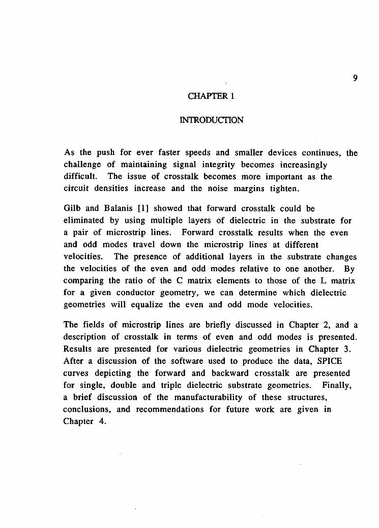
2.1 Fields
The electric and magnetic fields surrounding a single conductor
located above an infinite ground plane in a homogeneous medium
are shown in Figure 2-1. Assuming the current to be heading out of
the paper, the electric field lines travel from the conductor to the
ground plane. The fringing fields at the edges of the conductor
extend outward beyond the boundaries of the conductor. These
fringing fields will interact and couple with other conductors if they
are nearby. The magnetic field lines for the structure surround the
single conductor. These, too, extend beyond the boundaries of the
conductor and will interact with other nearby conductors.
Figure 2-1 Field lines for a single conductor in a homogeneous
medium located over a ground plane.
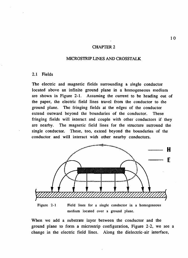
When we add a substrate layer between the conductor and the
ground plane to form a microstrip configuration, Figure 2-2, we see a
change in the electric field lines. Along the dielectric-air interface,
1 1
we see an additional bowing out of the fringing fields. This effect is a
result of the electric fields reconfiguring themselves to obey
Maxwell's equations inside each of the regions while maintaining
continuity conditions at the interface. The greater the dielectric
mismatch at the interface, the more exaggerated the effect.
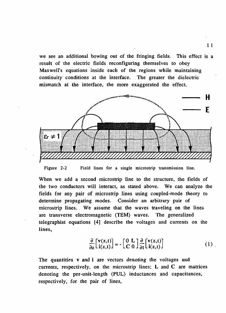
When we add a second microstrip line to the structure, the fields of
the two conductors will interact, as stated above. We can analyze the
fields for any pair of microstrip lines using coupled-mode theory to
determine propagating modes. Consider an arbitrary pair of
microstrip lines. We assume that the waves traveling on the lines
are transverse electromagnetic (TEM) waves. The generalized
telegraphist equations [4] describe the voltages and currents on the
lines,
The quantities v and i are vectors denoting the voltages and
currents, respectively, on the microstrip lines; L and C are matrices
denoting the per-unit-length (PUL) inductances and capacitances,
respectively, for the pair of lines,
Figure 2-2 Field lines for a single microstrip transmission line.
arvCM)! ro Li a_rv(z , t ) i 3zLi(z , t )J " L C 0 J at L i (z , t ) J
( i )
1 2
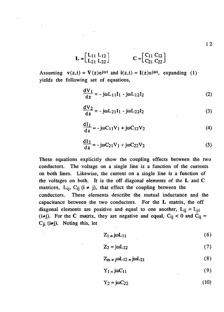
i _ l " L l l L l 2 l r -_rCllCl2l Ll2I L22J LC2I C22J
Assuming v(z,t) = V(z)ejwt and i(z,t) = I(z)ejwt, expanding (1)
yields the following set of equations,
dVi ~^~ = - jcoL 11I1 - JC0L12I2 (2)
dV2 dz = - jcoL2iIi - JC0L22I2 (3)
d l i • ^ -= - j a )CnVi+ jcoCi 2V2 (4)
^=-j(0C2lVl+j0)C22V2 (5)
These equations explicitly show the coupling effects between the two
conductors. The voltage on a single line is a function of the currents
on both lines. Likewise, the current on a single line is a function of
the voltages on both. It is the off diagonal elements of the L and C matrices, Ljj, Qj (i * j), that effect the coupling between the
conductors. These elements describe the mutual inductance and the
capacitance between the two conductors. For the L matrix, the off
diagonal elements are positive and equal to one another, Ly = Lji (i*j). For the C matrix, they are negative and equal, Qj < 0 and Qj =
Cji (i*j). Noting this, let
Zi = jcoLn (6)
Z2=jcoL22 (7)
Zm=jCoLi2=jcoL2i (8)
Yi . j f f lCn (9 )
Y2 =jcoC22 (10)
1 3
Ym =-jcoCi2 =-jcoC2i (11)
The Zj (i=l,2) denote the series impedance of each line, while the Yj
(i=l,2) denote the admittance of each line. Zm and Ym represent the
mutual impedance and admittance, respectively, between the two
lines. Rewriting equations (2) - (5) using using equations (6) - (10)
y i e lds
dVi = - Z i l i - Zml2 (12 )
dV2 " ^ -Zml i -Z 2 I 2 (13 )
^ = - YiV, - Y m V 2 (14 )
^ •= -Y m V! -Y 2 V 2 (15 )
By eliminating Ii and I2, we can reduce the four coupled equations,
(12) - (15) to a pair of coupled equations that relate the voltages on
the two microstrip lines. First, take the derivative with respect to z
of (12) and (13),
A')\T 1 AT t AJ^ (16)
(17 )
and then substitute (14) and (15) into (16) and (17). to obtain the
desired pair of coupled equations,
d2Vi - ^ •=a iVi+b iV 2 (18 )
d2V 1 dz2 ~
7 dli *dz
7 dl2
" d z
d2V2
dz2 ~~ v dl2
" Z 2 dz ^"dz
d2V2 d z 2 = a2V2 + b2Vi
14
(19)
where
a i = (Z iY i + Z m Y m ) (20 )
a2 = (Z2Y2 + ZmYm) (21)
b i = (Z iY m + Z m Y 2 ) (22 )
b2 = (Z2Ym + ZmY i) (23)
If we combine (18) and (19) (e.g., substitute Vi from (19) into (18)),
we arrive at the eigenvalue equation for the propagating modes,
(d4 d2 (dz? " ^ a 2 + a i ^dz2 + a l & 2 - b ib2 j V(z ) = 0 (24)
Assuming the voltage V(z) has the form Voe_Yz and substituting this
into (24), we arrive at the characteristic equation
Y 4 - ( a i + a 2 )Y 2 + a ia? , - b ib2 = 0 (25 )
The four roots of this equation are
\2,3,4 = ±yc'yn = ±y ai \ a2 1 2 V (al'a2)2 + 4bib2 (26)
where
Yc2 - ai 2 ^ +2 V(ai_a2)2 + 4blb2 (27)
Yji2 = ai 2 a2 " 2 V(ai"a2)2 + 4bib2 (28)
1 5
Yc and Yn are the propagation constants for the two propagating
modes, the c and k modes, of an arbitrary pair of coupled lines. The
positive and negative roots of each propagation constant correspond
to positive and negative traveling waves in each mode. If the
microstrip lines are identical, the structure symmetric and the generalized coupled modes, c and tc, will simplify to an even and an
odd mode.
The identical lines of a symmetric structure will have the same
impedances and admittances, Ln=L22 and Cn=C22- Hence, from (6) -
(11) and (20) - (23) above, ai = a2 and bi = b2. Applying this simplification to Yc and yn yields the propagation constants for the
even and odd modes,
Yc=Y e =±V0 + b ) =W( Y + Y m ) (Z + Z m ) (29 )
% = Yo = ±V( a " b ) =W( Y " Y m)( z " Z m ) (30 )
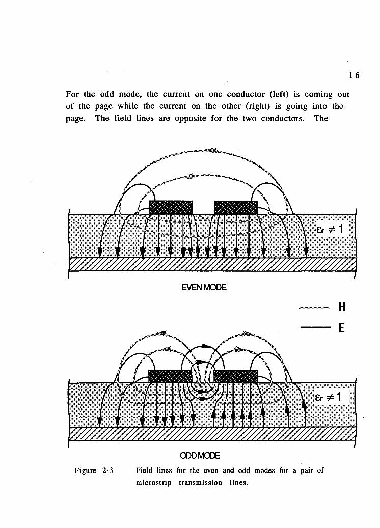
Figure 2-3 shows the field lines for the even and odd modes. For the
even mode, the current on each conductor is flowing out of the page
and the field lines for each conductor considered separately are the
same. The electric field lines begin on the conductors and end on the
ground plane, and the magnetic field lines surround the conductors
in a counterclockwise direction. Because the electric field lines for
each conductor are emanating from the conductor, they cancel each
other at the center of the structure, along the line of symmetry. This
mode exhibits no electrical coupling between the lines. Since the
magnetic fields for each conductor are in a counterclockwise
direction, they destructively interfere between the conductors, but
constructively interfere above and below them. Thus, each magnetic
field line encircles both conductors and the two microstrip lines are
magnetically coupled. Essentially, the even mode behaves as though
a magnetic wall lay along the line of symmetry.
1 6
For the odd mode, the current on one conductor (left) is coming out
of the page while the current on the other (right) is going into the
page. The field lines are opposite for the two conductors. The
"\ /
I " "•
T
EVEN MODE
H
4% J"" WW WW*
ODD MODE
Figure 2-3 Field lines for the even and odd modes for a pair of
microstrip transmission lines.
1 7
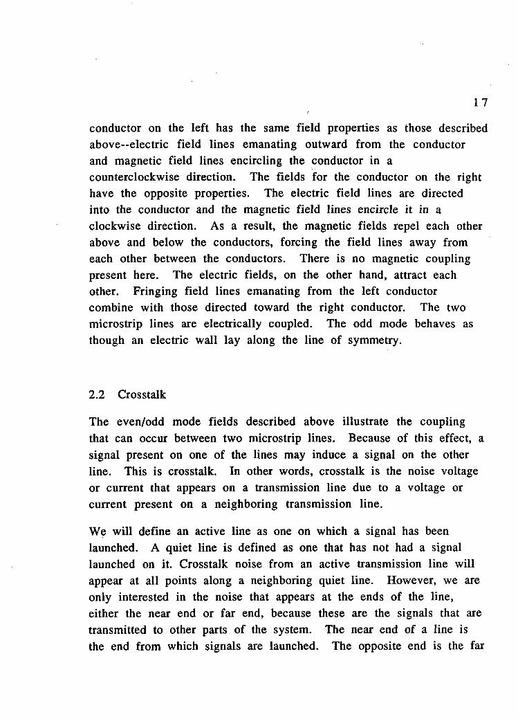
conductor on the left has the same field properties as those described
above—electric field lines emanating outward from the conductor
and magnetic field lines encircling the conductor in a
counterclockwise direction. The fields for the conductor on the right
have the opposite properties. The electric field lines are directed
into the conductor and the magnetic field lines encircle it in a
clockwise direction. As a result, the magnetic fields repel each other
above and below the conductors, forcing the field lines away from
each other between the conductors. There is no magnetic coupling
present here. The electric fields, on the other hand, attract each
other. Fringing field lines emanating from the left conductor
combine with those directed toward the right conductor. The two
microstrip lines are electrically coupled. The odd mode behaves as
though an electric wall lay along the line of symmetry.
2.2 Crosstalk
The even/odd mode fields described above illustrate the coupling
that can occur between two microstrip lines. Because of this effect, a
signal present on one of the lines may induce a signal on the other
line. This is crosstalk. In other words, crosstalk is the noise voltage
or current that appears on a transmission line due to a voltage or
current present on a neighboring transmission line.
We will define an active line as one on which a signal has been
launched. A quiet line is defined as one that has not had a signal
launched on it. Crosstalk noise from an active transmission line will
appear at all points along a neighboring quiet line. However, we are
only interested in the noise that appears at the ends of the line,
either the near end or far end, because these are the signals that are
transmitted to other parts of the system. The near end of a line is
the end from which signals are launched. The opposite end is the far
1 8
end. This means that the active line determines which end is
considered near and which is considered far, see Figure 2-4. We will
call the signals appearing at the near end of the quiet line backward crosstalk and those appearing at the far end of the quiet line
forward crosstalk.
Forward crosstalk is important because it occurs at the end of the
line that is connected to the next stage of the circuit. For instance,
consider the case where two adjacent microstrip lines are the digital
outputs of one circuit stage to the inputs of the next. Further,
assume that one of the lines is active while the other is quiet. If the
forward crosstalk is large enough, it is possible for the quiet line to
deliver a false high or low to the following input stage. Reducing the
forward crosstalk will lessen the chances of delivering a false signal.
Consider the modal fields shown in Figure 2-3. The field structures
for the two modes are very different. Because of this, we would
expect the modes to have different characteristics. This is indeed the
case. For this inhomogeneous structure, we find that the proportion
of E and H fields located in the air compared to the proportion
located in the substrate is different for the two modes. As a result,
the apparent inductance and capacitance of each mode are different,
and hence their characteristic impedances and velocities are
different. Expressed in terms of the modal inductances and
capacitances, the characteristic impedances and velocities are written
as follows,
(31)
(32)
1 9
1 Ve Vl^CT
(33)
1 Vo = Vl^
(34)
where Zo is characteristic impedance, v is velocity, L is inductance, C
is capacitance, and the subscripts e and o refer to the even and odd modes, respectively.
The even and odd modes are really just mathematical constructs to
describe the behavior of a signal traveling down a pair of coupled
transmission lines. Suppose we choose an even and an odd mode to
describe a signal as it appears at the beginning of a pair of lines. If
these modes behave differently as they travel down the lines, it
follows that at some distance down the lines the signal they describe
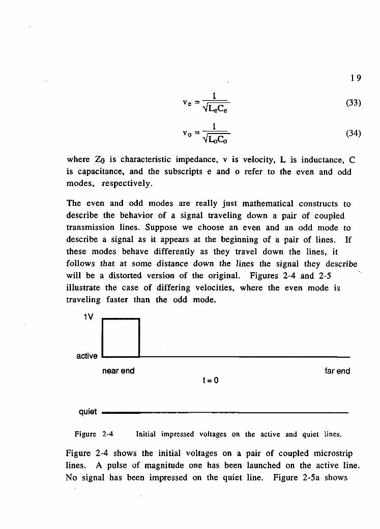
will be a distorted version of the original. Figures 2-4 and 2-5
illustrate the case of differing velocities, where the even mode is
traveling faster than the odd mode.
1V
active
near end far end t = 0
quiet
Figure 2-4 Initial impressed voltages on the active and quiet lines.
Figure 2-4 shows the initial voltages on a pair of coupled microstrip
lines. A pulse of magnitude one has been launched on the active line.
No signal has been impressed on the quiet line. Figure 2-5a shows
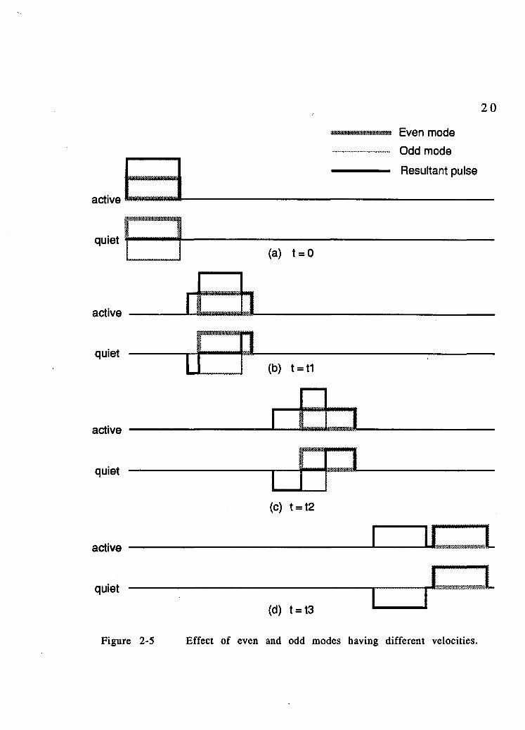
2 0
actjve iwwwwfflaawwwww
Even mode
Odd mode
Resultant pulse
quiet
active
quiet
active
quiet
active
quiet
(a) t-0
I rzi 2
(b) t = t1
MWMMMjl
(c) t = t2
(d) t = t3
inn
JUL
Figure 2-5 Effect of even and odd modes having different velocities.
2 1
how we can describe this scenario in terms of even and odd modes.
The even mode has a positive pulse on each line that is equal to half
the magnitude of the "real" pulse in Figure 2-4. The odd mode has a
positive pulse on the active line and a negative pulse on the quiet
line. Again, the magnitude of the pulses is equal to half that of the
"real" pulse. Initially, the modes lay on top of one another. Adding the voltages present on each line, we find that the active line has IV
and the quiet line has OV, corresponding to the pulses launched on
the lines.
Figure 2-5b shows the voltages on the lines after the pulses have
traveled a short distance. The modes no longer lay exactly on top of
each other. Assuming that the even mode has a higher velocity, we
see that it is slightly ahead of the odd mode. The even and odd
pulses on the quiet line do not exactly cancel each other any longer,
so we have a pair of noise pulses appearing. Also, the pulse on the
active line has spread out. Figures 2-5c to 2-5d show the pulse as it
travels further down the microstrip lines. If the lines are long
enough, the even and odd modes will completely separate into two
positive pulses on the active line and a positive and negative pulse
on the quiet line.
Recall, that velocity is defined as
where c is the speed of light. So, the velocity of a given mode is related to the effective dielectric constant of that mode, ere or ero. If
we can manipulate the effective dielectric constants of the modes, we
can manipulate their relative velocities. Gilb [1] showed that by
adding additional layers to the traditional single substrate microstrip structure, efe and ero can be made to equal each other. The effect of
1 c (35) v
2 2
this is to make the velocities of the two modes equal, thereby
eliminating forward crosstalk as described above.
A quick way of determining if a given combination of dielectrics and
their relative thicknesses will produce a structure where the modal
velocities are equal would be helpful. Under quasi-TEM conditions,
where the frequency dependence of v is negligible, this can be done
in the following manner. Setting the velocities in (33) and (34) equal
to one another, we find
So, when the ratio of the even to odd mode capacitances is equal to
the ratio of the odd to even mode inductances, the velocities of the
two modes will be equal and forward crosstalk will be minimized.
With this in mind, we must find a way to relate the even and odd
mode inductances and capacitances, Le,0 and Ce,o, to the inductance
and capacitance matrices for the structure. Consider again the propagation constants for the even and odd modes, Ye and Y0,
1 1 Ve VLeCe VLoCo V°
or,
Ce L (36)
Cq Le
Yc=Ye = ± V ( a + b ) = ± ^ / ( Y + Y r a ) ( Z + Z m ) (29)
(30)
and our definitions for Y and Z,
Zi = jwLn ( 6 )
Z2 = jcoL22 ( 7 )
2 3
Zm = jcoLn =jcoL2i
Yi =jcoCn
Y2 = jcoC22
Ym = -jcoCi2 = -jcoC2i
If we substitute (6) - (11) into (29) and (30), we find
Ce = Cn -1C12I
C0 = Cii + |Ci2[
Le = Ln + L12
L0 = Ln - L12
( 8 )
(9)
(10)
(11)
(39)
(40)
(41)
(42)
These expressions make intuitive sense if we look back to Figure 2-3.
The even mode shows magnetic (inductive) coupling between the
two conductors, but no electrical (capacitive) coupling. The odd mode
displays the opposite property—electrical (capacitive) coupling, but
no magnetic (inductive) coupling. If we substitute (39)-(42) into
(36) we find the following relationship,
Cn - C12
Cn + C12
L l l - L 1 2 L l l + L 1 2
or
rat - 1 rat - 1
rat + 1 L r a t + 1
(43)
where Crat Cn C12
L11 and Lrat = For (43) to be true, Crat = Lrat- So,
to determine what combination of materials and thicknesses will give
2 4
us a structure that minimizes forward crosstalk, we look at the ratio
of the first row of elements in the L and C matrices.
L is independent of the dielectric properties of the media. Because
we are dealing with non-magnetic materials, L is only a function of
conductor geometry. That is, it is dependent upon the conductor
width, thickness, seperation, and height above the ground plane only.
So, for a given conductor geometry, Lrat is fixed. Therefore, to satisfy
(43), it is necessary only to manipulate the dielectric permitivities
and thicknesses.
Throughout this development, all relative permitivities, er, were
assumed to be frequency independent constants. For high
frequencies this is not true. At some point, the frequency dependence of er cannot be ignored and dispersion effects must be
included for an accurate analysis. Let fg denote the maximum frequency for which er can be considered a constant. To produce
reliable results, then, one must be careful to apply this analysis only
when the contributing frequencies are less than fg. fg is
approximated by means of the empirical equation [8]
where ZLO is the characteristic impedance of a lossless line in free
space, h is the height of the conductors above the ground plane (in millimeters), ereff is the effective relative permitivity of the
structure, and Zl is the characteristic impedance of a lossless line. fg
is in gigahertz.
For example, a typical characteristic impedance for some of the structures discussed in the next chapter is ZL=80Q . Figure 2-6 shows a microstrip structure with the conductors located 0.66mm
(26mils) above the ground plane, the same height as those in next
(44)
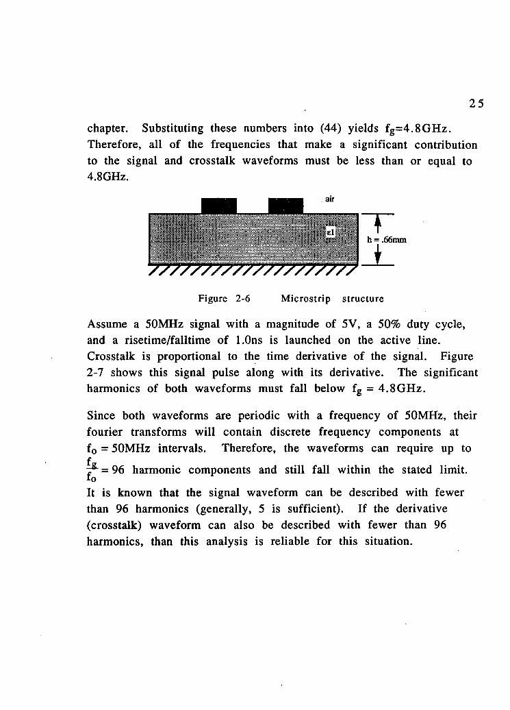
2 5
chapter. Substituting these numbers into (44) yields fg=4.8GHz.
Therefore, all of the frequencies that make a significant contribution
to the signal and crosstalk waveforms must be less than or equal to
4.8GHz.
h = .66mm
7/7/77/7////////77/7 Figure 2-6 Microstrip structure
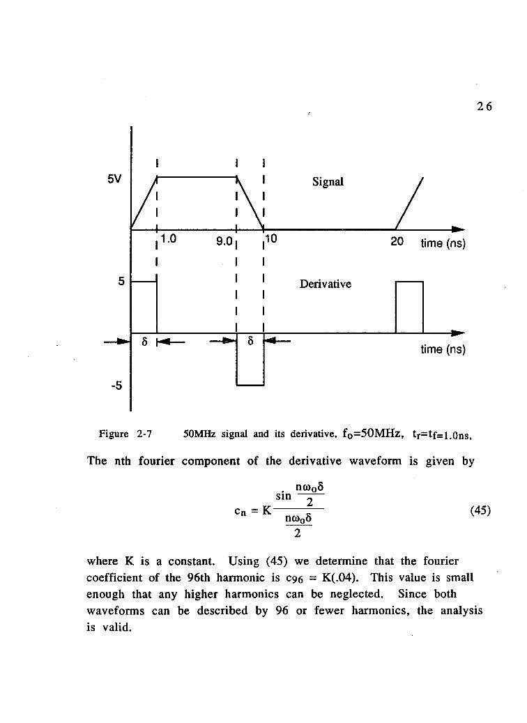
Assume a 50MHz signal with a magnitude of 5V, a 50% duty cycle,
and a risetime/falltime of 1.0ns is launched on the active line.
Crosstalk is proportional to the time derivative of the signal. Figure
2-7 shows this signal pulse along with its derivative. The significant
harmonics of both waveforms must fall below fg = 4.8GHz.
Since both waveforms are periodic with a frequency of 50MHz, their
fourier transforms will contain discrete frequency components at
f0 = 50MHz intervals. Therefore, the waveforms can require up to f 7s" = 96 harmonic components and still fall within the stated limit. to It is known that the signal waveform can be described with fewer
than 96 harmonics (generally, 5 is sufficient). If the derivative
(crosstalk) waveform can also be described with fewer than 96
harmonics, than this analysis is reliable for this situation.
2 6
5V Signal
1 0 9.0 10 20 time (ns)
Derivative
time (ns)
-5
Figure 2-7 50MHz signal and its derivative, fo=50MHz, tr=tf=l.0ns,
The nth fourier component of the derivative waveform is given by
nci)0§ sin -z—
c » = ( 4 5 )
2
where K is a constant. Using (45) we determine that the fourier
coefficient of the 96th harmonic is C96 = K(.04). This value is small
enough that any higher harmonics can be neglected. Since both
waveforms can be described by 96 or fewer harmonics, the analysis
is valid.
2 7
CHAPTER 3
RESULTS AND DISCUSSION
3.1 Software
Three steps were required to produce the results in the following
sections. First, in order to determine Crat and Lrat» inductance and
capacitance matrices had to be calculated for the considered
geometries. Second, these L and C matrices had to be converted into
useful transmission line circuits. Third, the effect of these circuits on
input signals had to be simulated.
The first of these steps was completed using a program called
UAMOM. UAMOM was developed at the University of Arizona. As
input, the program accepts a description of the two-dimensional
cross-section of a structure and assumes that the structure is infinite
in length. UAMOM assumes a TEM wave propagation mode, and uses
the method of moments to solve Lapace's equation in two
dimensions. Using the concept of total charge, UAMOM calculates the
capacitance matrix, C, of the the n-conductor system. Qj is the free
charge PUL on the ith conductor due to a 1 volt potential on the jth conductor when all other conductors are grounded. Cajr is then
calculated, where Cajr is the capacitance matrix for the system when
all relative dielectric permitivities are set equal to one. The
inductance matrix, L, is then found from the relationship
L = HOEO(CAIR)"1 (46)
where |io and eo are the free space permeability and permitivity,
respectively, and (Ca,,.)"1 is the inverse of the matrix Cair.
UAMOM has a weakness that must be taken into account when using
its data. When adjacent dielectrics have relative permitivites that
2 8
are very close to one another, the L and C matrices calculated by
UAMOM are not reliable. For this reason, cases which include
adjacent dieletrics whose difference in relative permitivity values is
less than or equal to one were not considered for simulation.
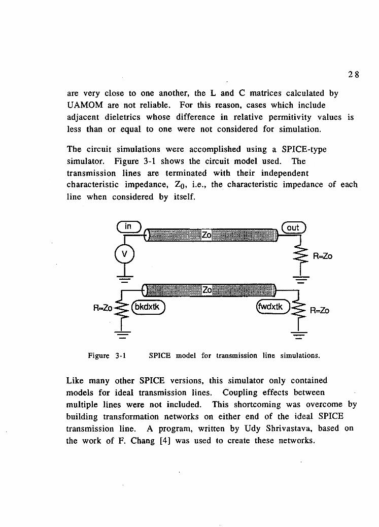
The circuit simulations were accomplished using a SPICE-type
simulator. Figure 3-1 shows the circuit model used. The
transmission lines are terminated with their independent characteristic impedance, ZQ, i.e., the characteristic impedance of each
line when considered by itself.
(fwdxtk )% R=Zo
Figure 3-1 SPICE model for transmission line simulations.
Like many other SPICE versions, this simulator only contained
models for ideal transmission lines. Coupling effects between
multiple lines were not included. This shortcoming was overcome by
building transformation networks on either end of the ideal SPICE
transmission line. A program, written by Udy Shrivastava, based on
the work of F. Chang [4] was used to create these networks.
2 9
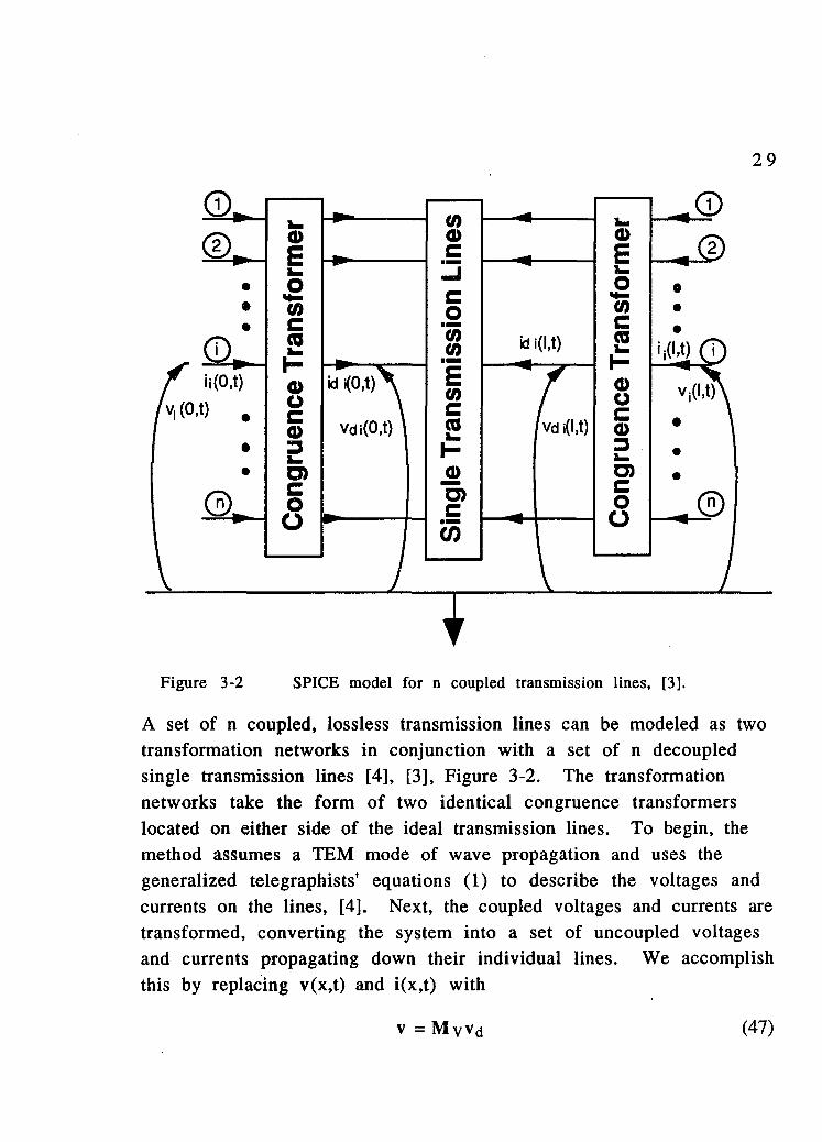
ii(O.t) id <0,t) VJ(l,t)
vd i(l,t)
O) D)
Figure 3-2 SPICE model for n coupled transmission lines, [3].
A set of n coupled, lossless transmission lines can be modeled as two
transformation networks in conjunction with a set of n decoupled
single transmission lines [4], [3], Figure 3-2. The transformation
networks take the form of two identical congruence transformers
located on either side of the ideal transmission lines. To begin, the
method assumes a TEM mode of wave propagation and uses the
generalized telegraphists' equations (1) to describe the voltages and
currents on the lines, [4]. Next, the coupled voltages and currents are
transformed, converting the system into a set of uncoupled voltages
and currents propagating down their individual lines. We accomplish
this by replacing v(x,t) and i(x,t) with
v = M yVd (47)
3 0
i = Miid (48)
where M v and Mi are n x n constant matrices, and substituting these into (1). This gives us
_a_rvd(z,t)i _ r o Ld"| a_rvd(z,t)i a z L i d ( z , t ) J _ " L c d o J a t L i d ( z , t ) J < 4 9 >
Vd and id are now decoupled and Ld and Cd are the modified
inductance and capacitance matrices that describe this new
decoupled arrangement. The time delay and characteristic
impedance matrices can be calculated from Ld and Cd as follows,
I Dd = (LdCd)2 (50)
i Zd = (Ldcd)2 Cd-' (51)
where Dd is the time delay matrix, Zd is the characteristic impedance
matrix, and both are diagonal. Now by applying the values in the Dd
and Zd matrices to n SPICE transmission lines, and using the
networks at both ends of the lines to transform the voltages and
currents from coupled space to uncoupled space, we can simulate n
coupled transmission lines. The following algorithm describes how to
determine the values for circuit, [3],
1. Given the number of lines n, compute the eigenvalues of matrix LC, A,j.
2. Compute the matrix My = [Mjj] of right eigenvectors of LC.
3. i= 0.
4. i = / +1; compute the control law for each dependent source of
the tranformation network using the following equations, (see
Figure 3-3):
3 1
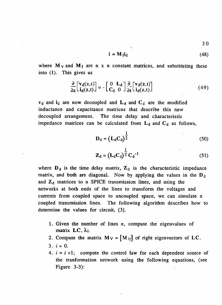
vsi(x,t) = nMijVdj(x,t) - vdj(x,t)
isi(x,t) = . 2 Mijid;(x,t) - idj(x,t) i=l-»n J J
( 5 2 )
( 5 3 )
where either x=0 or x=l, 1 being the length of the line. 5. Compute the characteristic impedance Zdj and the time delay
per unit length Dd, of the ith line using (50)-(51).
6. If i<n go to Step 4; else stop.
" (o.ty Vsi (0,t)
-o-
Vi isi (0,t)(] ^ Vdi (0,t)
Idi (0,t) —• 0
Vsi (I ,t) Idi (I ,t)
-•—4 o— ii (i ,t)
Vdi (I ,t) (j )isi (I ,t) Vi (I ,t)
Figure 3-3 Detailed model for the ith line [3],
3.2 Geometries
Three geometries are examined here. In all of them, conductor
thickness, spacing, and height above ground is kept constant to
maintain a consistent inductance matrix throughout. The only
changes occurring are changes in dielectric type and placement.
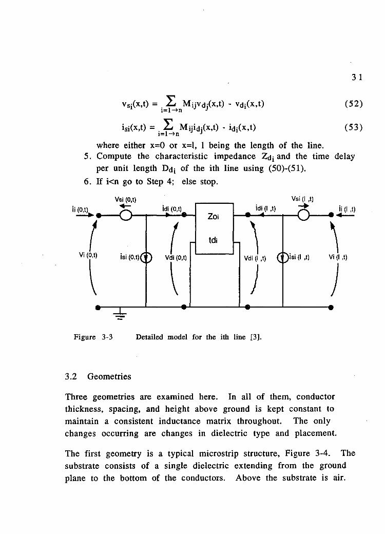
The first geometry is a typical microstrip structure, Figure 3-4. The
substrate consists of a single dielectric extending from the ground
plane to the bottom of the conductors. Above the substrate is air.
y/t
h=26mil t=2.25mil wl=w2=2.5mil s=1.25mil
Figure 3-4 Single dielectric substrate geometry.
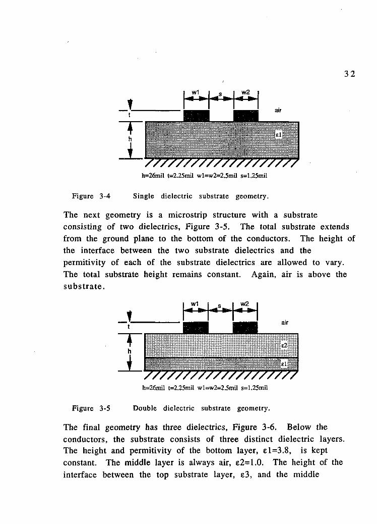
The next geometry is a microstrip structure with a substrate
consisting of two dielectrics, Figure 3-5. The total substrate extends
from the ground plane to the bottom of the conductors. The height of
the interface between the two substrate dielectrics and the
permitivity of each of the substrate dielectrics are allowed to vary.
The total substrate height remains constant. Again, air is above the
s u b s t r a t e .
iMt®
h=26mil t=2.25mil wl=w2=2.5mil s=1.25mil
Figure 3-5 Double dielectric substrate geometry.
The final geometry has three dielectrics, Figure 3-6. Below the
conductors, the substrate consists of three distinct dielectric layers. The height and permitivity of the bottom layer, e 1=3.8, is kept
constant. The middle layer is always air, e2=1.0. The height of the
interface between the top substrate layer, E3, and the middle
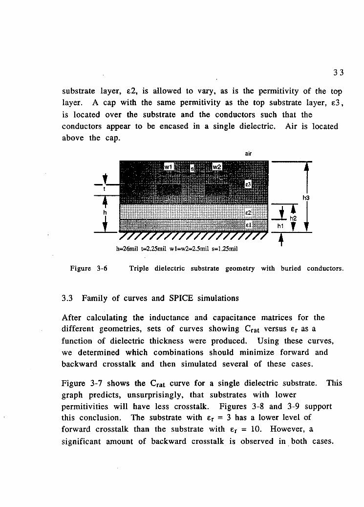
3 3
substrate layer, e2, is allowed to vary, as is the permitivity of the top
l a y e r . A c a p w i t h t h e s a m e p e r m i t i v i t y a s t h e t o p s u b s t r a t e l a y e r , e 3 ,
is located over the substrate and the conductors such that the
conductors appear to be encased in a single dielectric. Air is located
above the cap.
air
M f V ////////////////////
h=26mil t=2.25mil wl=w2=2.5mil s=1.25mil
Figure 3-6 Triple dielectric substrate geometry with buried conductors.
3.3 Family of curves and SPICE simulations
After calculating the inductance and capacitance matrices for the different geometries, sets of curves showing Crat versus er as a
function of dielectric thickness were produced. Using these curves,
we determined which combinations should minimize forward and
backward crosstalk and then simulated several of these cases.
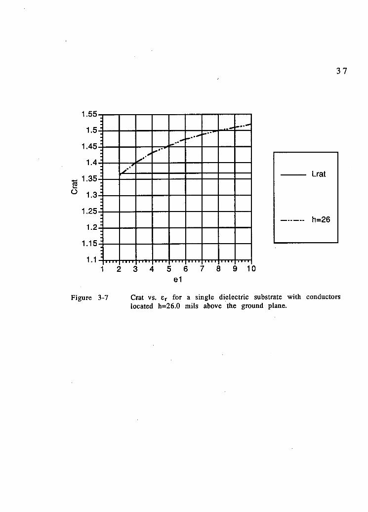
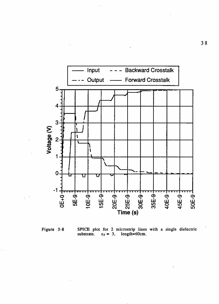
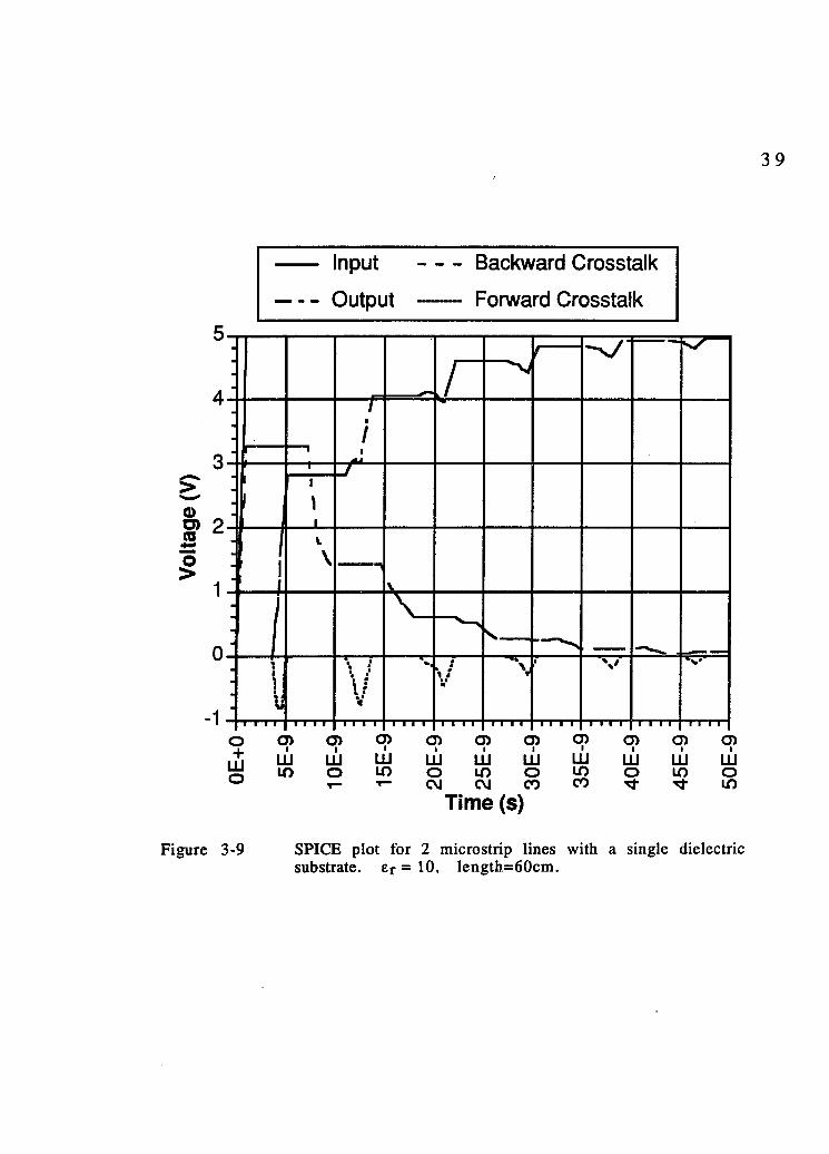
Figure 3-7 shows the Crat curve for a single dielectric substrate. This
graph predicts, unsurprisingly, that substrates with lower
permitivities will have less crosstalk. Figures 3-8 and 3-9 support this conclusion. The substrate with er = 3 has a lower level of
forward crosstalk than the substrate with er = 10. However, a
significant amount of backward crosstalk is observed in both cases.
3 4
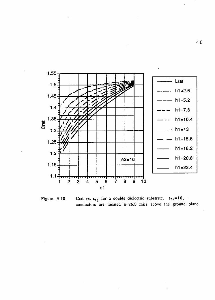
Next we present sets of Crat curves for the double dielectric substate,
Figures 3-10 to 3-12. Because the addition of a low permitivity dielectric decreases the effective er of the substrate, all of the points
which have a low permitivity dielectric beneath a high permitivity
one will show a lower level of forward crosstalk than their single
high permitivity dielectric counterpart. As the value of Crat gets
closer to Lrat, the difference in the even and odd mode velocities
approaches zero and the forward crosstalk disappears. This trend is
illustrated in Figures 3-13 and 3-14, where we have chosen to simulate two points from the family of curves for Er2 =10 Figure 3-
13 represents the point located at eri =3 and hi = 10.4, and Figure 3-
14 is from the point £rl =3 and hi = 13.0. The forward crosstalk
decreases as we move from Figure 3-13 to 3-14, but there is no
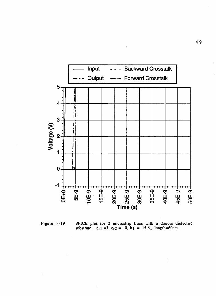
signifcant change in the backwards crosstalk. The same trend is s h o w n i n F i g u r e s 3 - 1 5 a n d 3 - 1 6 , w h e r e e r 2 = 8 .
The cases shown in Figures 3-13 through 3-16 all have Crat greater
than Lrat. When we cross over the Lrat line such that Crat becomes
less than Lrat, the backward crosstalk disappears, see Figures 3-17
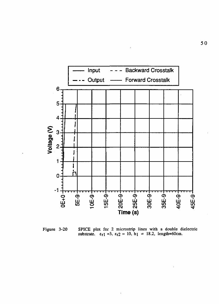
through 3-20 The forward crosstalk increases as we move away
from the Lrat line. If we choose a pair of dielectrics and select their heights such that Crat ^ Lrat, we can minimize both forward and
backward crosstalk.
In all of the simulations discussed thus far, the transmission lines
had approximately matched terminations at both ends of the quiet
line and at the receiving end of the active line as shown in Figure 3-
1. If the terminations are not matched, we would expect forward
crosstalk to reappear. Reflections due to a mismatch on the active
line are like newly lauched signals, producing both near end and far
end crosstalk noise. A reflection occurring at the receiving end of the
active line will induce near end crosstalk at the receiving end of the
quiet line. Since that is where we measure forward crosstalk, we see
3 5
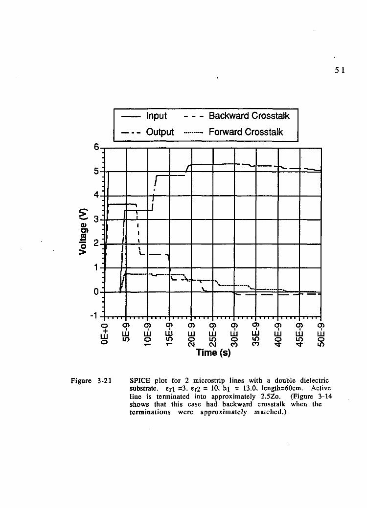
noise reappearing there, Figure 3-21. Mismatches on the quiet line
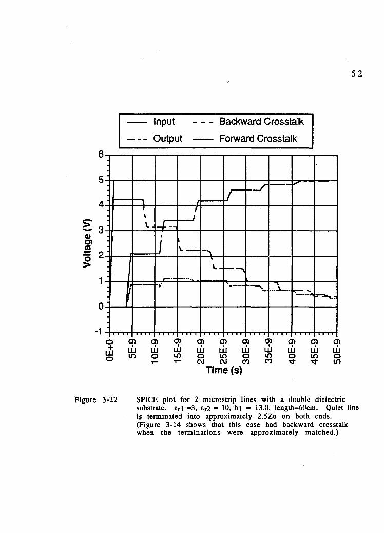
will permit multiple relfections of any voltages induced on the line,
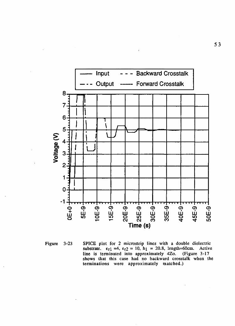
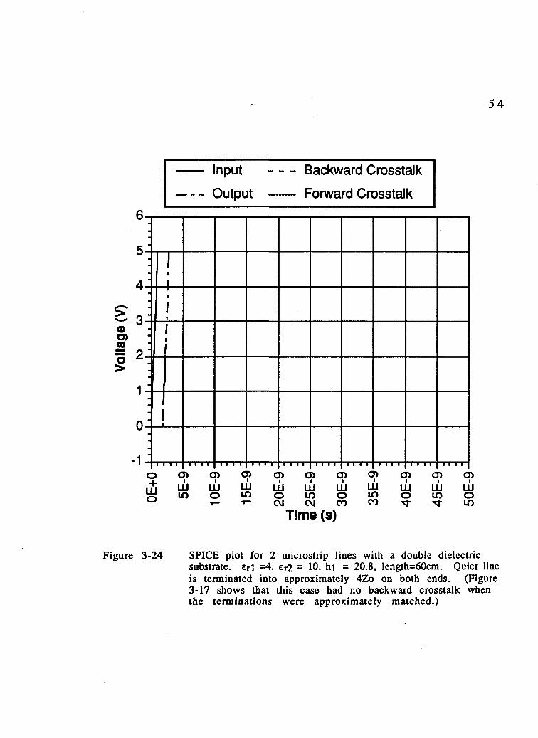
Figure 3-22. Neither Figure 3-23 nor 3-24 shows crosstalk for a
mismatched termination. This was a case where both the backward
and forward crosstalk were negligible. Without either of these noise
sources, there was no mechanism available to increase the crosstalk.
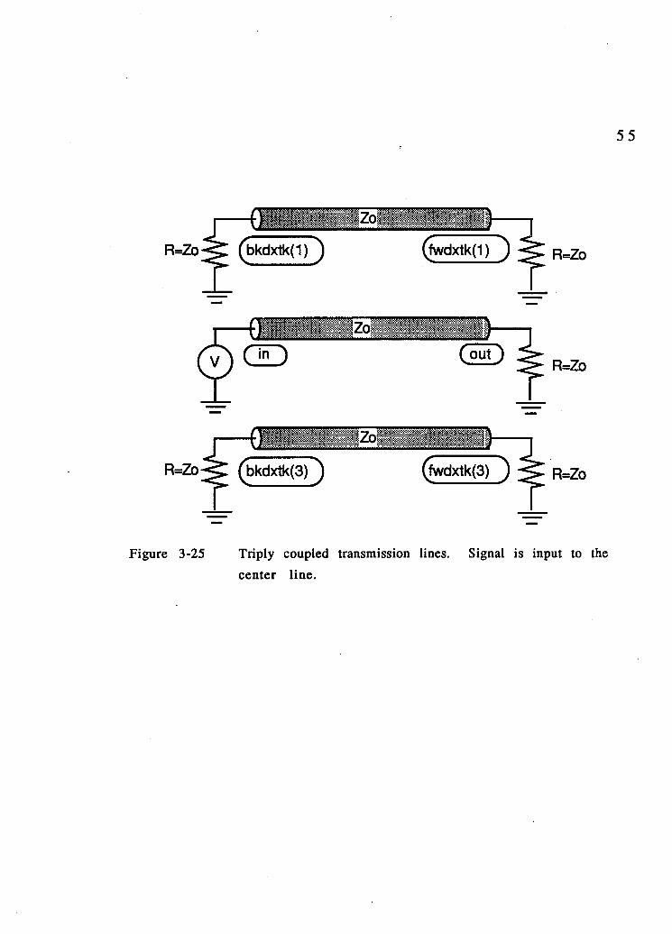
Simulations were also completed for triply coupled lines to show the
effect of adding a third line. In each case, the line terminations were
approximately matched for the three individual lines. The addition
of the third line had a similar effect whether or not the doubly
coupled model had exhibited backward crosstalk. When a signal is
impressed on the center line, Figure 3-25, the crosstalk on the two
outer lines is identical. Figure 3-27 is a case where Crat was greater
than Lrat for the doubly coupled lines. For the case shown in Figure
3-28, Crat was less than Lrat for the for the doubly coupled lines.
Because the surrounding lines affect the impedance of the individual
microstrip lines, our terminations are not truly matched. This is
shown by the fact that the output of the middle lines needs multiple
reflections to build up to its steady state value.
When we impress the input signal on one of the end lines, Figure 3-
26, we see backward crosstalk on line 2 and forward crosstalk
appearing on line 3, Figures 3-29 and 3-30. The addition of a third
microstrip line makes it necessary to use three modes to describe all
the possible signals on the lines. However, in choosing the dielectrics
and their thicknesses in this example, only two modes were
considered. If the middle line is active, Figures 3-25, 3-27 and 3-28,
modes that approximately resemble the symmetric and anti
symmetric even and odd modes are excited. The crosstalk resembles
that for the doubly coupled cases. However, if one of the outside
lines is the active line, the modes describing the signals on the outer
3 6
lines do not resemble the even and odd modes so forward crosstalk
is not minimized.
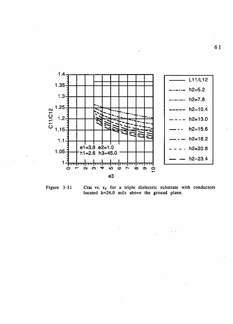
The Crat curves for the triple dielectric buried microstrip does not
indicate any cases where the forward crosstalk will be eliminated.
The layer of air in the substrate reduces the Crat to such a degree
that, for this conductor geometry, it is always less than Lrat- This
complete mismatch between Crat and Lrat might be removed by
either changing the air layer to some dielectric or by changing the
conductor geometry.
3 7
2 o
1.55-
1.5-
1.45-
1.4-
1.35-
1.3-
1.25-
1.2-
1.15-
1.1- rrrr fTT
2 3 4 5 6 7 8 9 1 0 e1
Lrat
h=26
Figure 3-7 Crat vs. er for a single dielectric substrate with conductors located h=26.0 mils above the ground plane.
Input - - Backward Crosstalk
Output — — Forward Crosstalk
5
4
3
o > 1
0
j —J —J
I 1
F \ \
\ \ \
1
\_ X_
Lf \J V
O) O) CT) |
a Oi o) o> o> CT) CT)
Lii LLI LU LU LU LU LU LU LLJ LLJ LO O LO O LO o LO O in O
•»— CM CM CO Time (s)
CO in
Figure 3-8 SPICE plot for 2 microstrip lines with a single dielectric substrate. er = 3, length=60cm.
3 9
Input - - Backward Crosstalk
Output -— Forward Crosstalk
JL ^4 -N/ £7"
<D O) 2-(0
-1
\ 1 i
I I I I V I I I I I I I I I I I I I I O +
LU O
Oi o> O) O) O) O) C T ) 1 O) <y> o>
LU LLI LU LU LLJ LU LU LU LU LU m O m O in O in o m O
(M CM 00 CO in Time (s)
Figure 3-9 SPICE plot for 2 microstrip lines with a single dielectric substrate. er = 10, length=60cm.
4 0
re u . o
1.55
1.5
1.45
1.4
1.35
1.3
1.25
1.2
1.15
1 . 1
.J i
>
#
/ • " t
/
* /
• -X
3
'<-4 r, f' / 9 t . % •'/
4—
•i 7 w
e; 2=1 C
2 3 4 5 6 7 8 9 1 0 e1
Lrat
h1=2.6
h1=5.2
h1=7.8
h1=10.4
hi=13
h1=15.6
h1=18.2
h1=20.8
h1=23.4
Figure 3-10 Crat vs. eri for a double dielectric substrate. er2=10>
conductors are located h=26.0 mils above the ground plane.
4 1
1.55
(0 o
ffl
e2 =9
rm rm rm rm
Lrat
h1=2.6
h1=5.2
h1=7.8
h1=10.4
hi=13
hi =15.6
hi =18.2
hi =20.8
hi =23.4
Figure 3-11 Crat vs. eri for a double dielectric substrate. 6^=9,
conductors are located h=26.0 mils above the ground plane.
4 2
1.55
1.45-
1.35 CO
o
1.25-
TTTT
e1
Lrat
h 1 =2.6
h1=5.2
h1=7.8
h1=10.4
h 1 = 13
h1=15.6
h 1 =18.2
h1=20.8
hi =23.4
Figure 3-12 Crat vs. eri for a double dielectric substrate. £r2=8.
conductors are located h=26.0 mils above the ground plane.

4 3
Input - - Backward Crosstalk
Output --— Forward Crosstalk
i J
r
W=r "\
x_ _
XT •S3
M i l I I I tt nrr tt I I I tt II I tt
o +
LU O
CD O) O) CD LU UJ LU LU 10 o m o
1- T— cvj
a) I LU m c\j
CD Oi o> CD 1 O) LU LU UJ UJ LU o LO o m o CO CO LO
Time (s)
Figure 3-13 SPICE plot for 2 microstrip lines with a double dielectric substrate. erl =3, er2 =10, hi = 10.4, length=60cm.
44
Input - - Backward Crosstalk
Output — — Forward Crosstalk
/ /
r '
t i i i
1
i i \
\
1 1
1 *
v _ —• -•»
.
1 1 1 1
Q) ^ o> 2 w o >
0
o +
LU O
a> o> O) 1 CD O) cr> CD 1
ill LLl LU LU LU LLl LU io O in o in O in
t— t- CM CM CO CO
Time (s)
CD LU O
a I LU lO
cn LU O in
Figure 3-14 SPICE plot for 2 microstrip lines with a double dielectric substrate. erl =3, er2 =10, hi = 13.0, length=60cm.

4 5
Input - - Backward Crosstalk
Output -— Forward Crosstalk
5-
4- •f
a> ^ O) 2-CO o >
1-
0-
t=;
v___ V
-1 I I I tt tt
o +
LU
o> i LU in
i i i i i i i i t
0 ) 0 ) 0 )
LU 111 LLI O lO o
CM
O) I LU m OJ
a> l LLI O CO
O) I LU in CO
Time (s)
t I I I I I I I I O) O) O) LLJ LU LU o in o t ^ m
Figure 3-15 SPICE plot for 2 microstrip lines with a double dielectric substrate, erl =3, er2 = 8, hi = 15.6, length=60cm.
4 6
Input - - Backward Crosstalk
Output — Forward Crosstalk
1 1 i i 1 1 1 1 1 1 i i 1 1 1 i i 1 1 1 1 1 1 1 1 1 1 1 i 1 1 i 1 1 1 1 — 1 1 1 1 O) o> o 1 cp O O) O) 1 O) cp O) LLI LLI LLI LLI LLI LLI LU LU LLI LLI LO O m O lO O in O in O
T— •<— CM CM CO CO Tj- in Time (s)
Figure 3-16 SPICE plot for 2 microstrip lines with a double dielectric substrate. eri =4, ej-2 = 8, hj = 23.4, length=60cm.

4 7
Input - - Backward Crosstalk
Output -— Forward Crosstalk
Q) ^ O) 2 & o >
0
-1
/ i
i
• 1
t 1 i i
i i 1 i 1 1
o +
111 o
o> CT> o> 1 Oi O) O) Ol |
o> O) CD LLI LLI LLI LLI LLI LLI LLI LLI LLI LLI in O in O in O in O m O
T— CM CM CO CO "<fr in Time (s)
Figure 3-17 SPICE plot for 2 microstrip lines with a double dielectric substrate, erl =4, er2 = 10, hi = 20.8, length=60cm.

4 8
Input - - Backward Crosstalk
Output -— Forward Crosstalk
A
I I 1 1 1 / 1
O "
1
/ I 1
i
i
0 "
1 1
1
1 " 1 1 1 1 1 1 1 1 1 1 1 1 o +
LLi O
CJ> o> O) i
O) q> O) O) t
O) <J> O) UJ LLI LLI LLI LLJ LLI LU LLJ 111 LLi U) O m o in O in o in O
V— CM CM CO CO m Time (s)
Figure 3-18 SPICE plot for 2 microstrip lines with a double dielectric substrate. eri =3, er2 = 9 hi = 15.6, length=60cm.
4 9
Input - - Backward Crosstalk
Output — — Forward Crosstalk
i i
i
i 1
1
1 i i
i h_
o +
LU O
O) o> o> 1 a CD <J) O)
| O) cp a
LLI LLi LU LU LLI LLI LU ih LU LLI in o in o in O in o in o
T~ T— CVJ CM CO CO in Time (s)
Figure 3-19 SPICE plot for 2 microstrip lines with a double dielectric substrate, erl =3, er2 = 10, hi = 15.6,, length=60cm.
5 0
Input - - Backward Crosstalk
Output -— Forward Crosstalk
1 1
i i i
I | 1
I 1 i n
o +
LLI O
O) i LU m
a O) o 1 O)
i O) O) C> CD
til UJ LU LLI LLI LLI LLI UJ o LO O m O to O in
CM CM CO CO
Time (s)
Figure 3-20 SPICE plot for 2 microstrip lines with a double dielectric substrate, erl =3, £r2 = 10, hi = 18.2, length=60cm.
5 1
Input - - Backward Crosstalk
Output -— Forward Crosstalk
© - J o> - f <o •
I 2 i '
1-
o-
. ..
-1 111—11 > o +
LU O
i i i i i i i 11 11 i i i tt I I I II I I o> o o
1 q> 9 o> O)
| Oi <J) o>
LU LLJ LU UJ LU LU LU LU 111 LU o in o LO O m o in O T- CM CM CO CO in
Time (s)
Figure 3-21 SPICE plot for 2 microstrip lines with a double dielectric substrate. erl =3, er2 = 10, hi = 13.0, length=60cm. Active line is terminated into approximately 2.5Zo. (Figure 3-14 shows that this case had backward crosstalk when the terminations were approximately matched.)
5 2
Input - - Backward Crosstalk
Output -• — Forward Crosstalk
2 3 0) O) (0 — 2 o * >
1
0
-1
—{ r / /
—1—
\. . 4-i
T i /
a
1 i v. _>v
: \
L -i.
-»• —v. —% w— — *,
o +
LU O
o> en O) 1 O) O) CD O)
1 CJ) CT)
LU ULl LU LU LU LU LU LLl LLl LU in O LO o in O un o lO O
T— "i— C\J CM CO CO in Time (s)
Figure 3-22 SPICE plot for 2 microstrip lines with a double dielectric substrate. erl =3, er2 = 10, hi = 13.0, length=60cm. Quiet line is terminated into approximately 2.5Zo on both ends. (Figure 3-14 shows that this case had backward crosstalk when the terminations were approximately matched.)
5 3
Input - - Backward Crosstalk
Output -— Forward Crosstalk
8
7
6
5
0) ** D) £ 3 o >
2
1
0
-1
1 r I
j 1 1
j 1 i \
! 1 1 1
I !
: i U
i ' 1
11 M 1 1 1 1 1 1 1 1 1 1 1 1 • 1 1 1 • • • I o +
LU O
CD o> O) 1
o> CD o> O) 1 CJ) CD CT)
LU LU LU LU LU LU LU LU LU LU o in O in O in O m o
•*— C\J CM CO CO xT in Time (s)
Figure 3-23 SPICE plot for 2 microstrip lines with a double dielectric substrate. erl =4, er2 = 10, hi = 20.8, length=60cm. Active line is terminated into approximately 4Zo. (Figure 3-17 shows that this case had no backward crosstalk when the terminations were approximately matched.)
5 4
Input - - Backward Crosstalk
Output -— Forward Crosstalk
5
4
S 3 <D O) (0 — 2 o * >
1
0
-1
l i 1 a
1 «
/ i
1
o +
111 o
o> o> o> 1 Oi CJ) CJ) Oi
1 a <ji o> 111 LU LLI LLI LLI LLI LU LU UJ LU in O un O in o in o in O
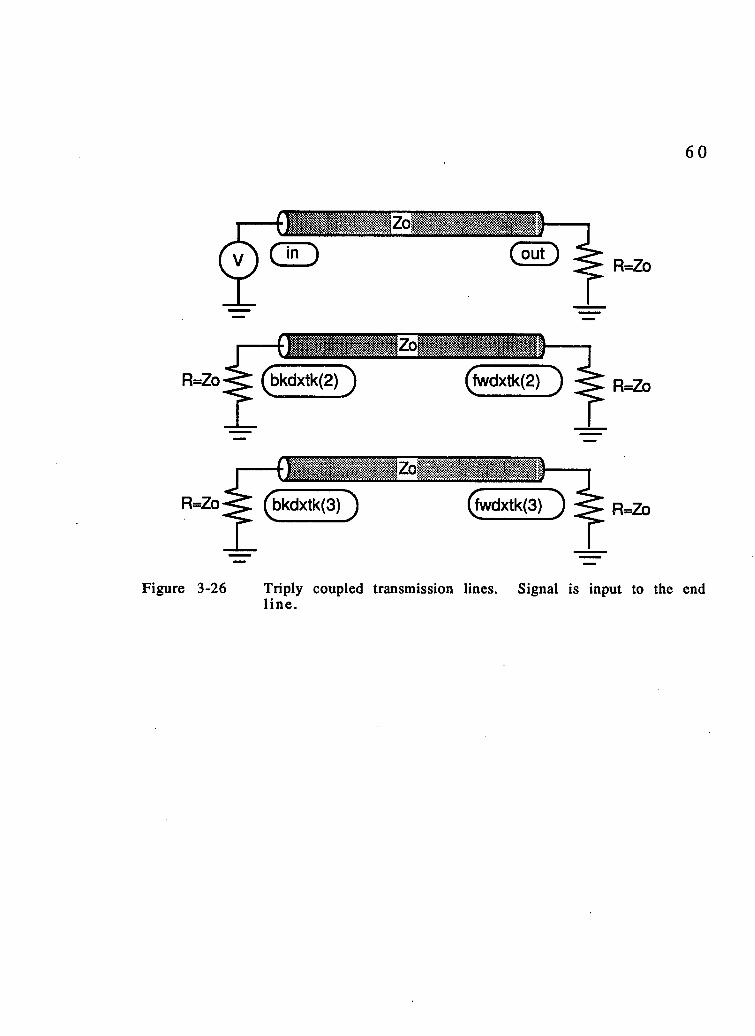
t— t— CM CVJ CO CO M- TJ- m
Time (s)
Figure 3-24 SPICE plot for 2 microstrip lines with a double dielectric substrate. erl =4, er2 = 10, hi = 20.8, length=60cm. Quiet line is terminated into approximately 4Zo on both ends. (Figure 3-17 shows that this case had no backward crosstalk when the terminations were approximately matched.)
5 5
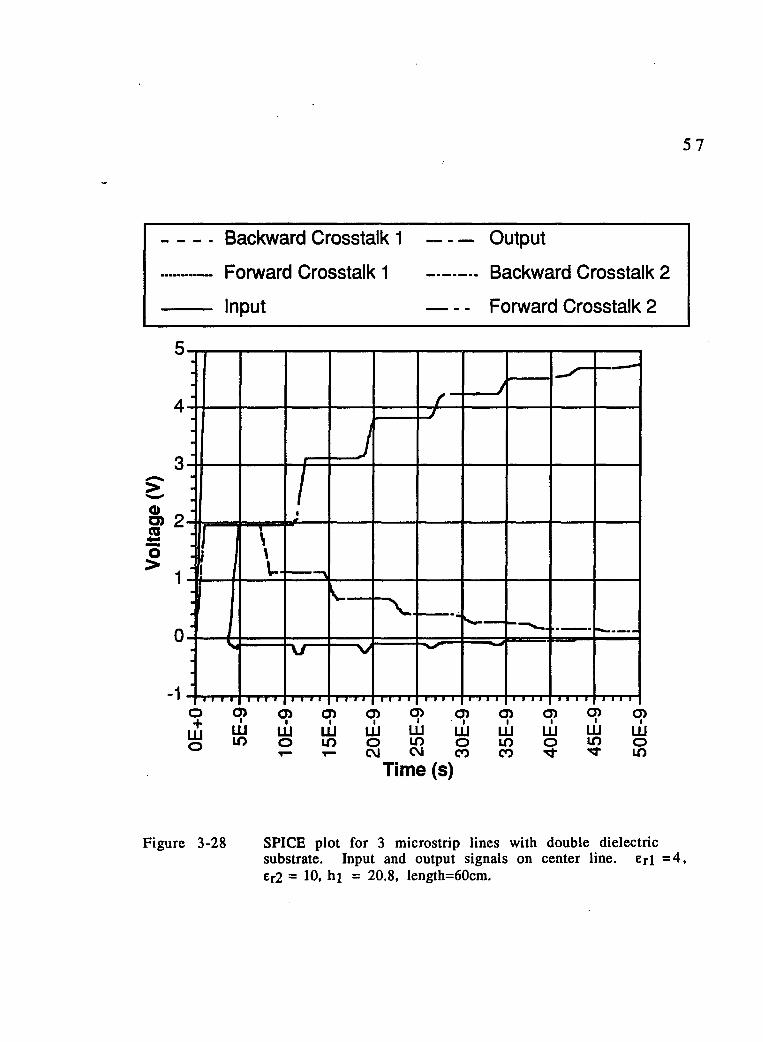
R=Zo (bkdxtk(1) ) (fwdxtk(1) ) < R=Zo
(°hD R=Zo
R=Zo- (bkdxtk(3) )
1-
(fwdxtk(3) ) R=Zo
Figure 3-25 Triply coupled transmission lines. Signal is input to the
center line.
5 6
Backward Crosstalk 1 Output
—— Forward Crosstalk 1 Backward Crosstalk 2
Input Forward Crosstalk 2
o : i
n
u
I I II
V
I I I I I I I I I I
A,'
x
l l l l
7
V
IT I I I
r S
o +
LU O
O) •
111 in
O) o> O) cn 1
O) O) o> LLJ LU LU LU LU LU LU O LO O LO O LO O
t— CM CM CO CO
1 1 1 1 1 M 1 1 1 1 1 1 1 o> LLJ LO
O) LLJ O in
Time (s)
Figure 3-27 SPICE plot for 3 microstrip lines with double dielectric substrate. Input and output signals on center line. erl =3, er2 = 10, hi = 13.0, length=60cm.
5 7
Backward Crosstalk 1 Output
— Forward Crosstalk 1 Backward Crosstalk 2
Input Forward Crosstalk 2
o> • O) O) cn O) i
O) O) O) O) 1
<j> LU LU LU LU LU LU UJ LU UJ UJ
O in o in o in o in o CM CM CO CO in
Time (s)
Figure 3-28 SPICE plot for 3 microstrip lines with double dielectric subs tra te . Input and output s igna l s on center l ine . e r l =4 , er2 = 10, hi = 20.8, length=60cm.
5 8
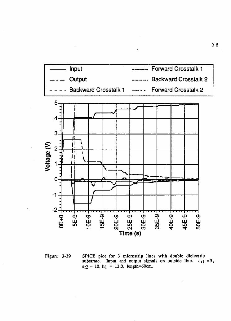
Input Forward Crosstalk 1
Output Backward Crosstalk 2
Backward Crosstalk 1 — . - - Forward Crosstalk 2
5-
4-
3-
2 2. G) D> (0 % 1->
0-
- 1 -
- 2 -
o +
LU O
TT TT
JL
TT
f
TT
-m/
y"
-TT
X
TT I I I I T o O) CD CD O) cp CD | o CD CD
LU LU LU LLI LU LLI LU LU LLI LJJ un o m O in O m o m o T— CM CM CO CO in
Time (s)
Figure 3-29 SPICE plot for 3 microstrip lines with double dielectric substrate. Input and output signals on outside line. erl =3, er2 = 10, hi = 13.0, length=60cm.
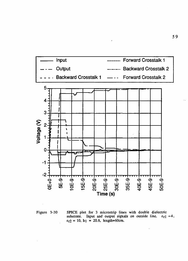
Input Forward Crosstalk 1
Output Backward Crosstalk 2
Backward Crosstalk 1 -— Forward Crosstalk 2
I I I I o> o> o>
1 O) O) o O) i CD Oi G)
LU LU LU UJ LU LU LU LU 111 LU lO O m o LO O LO O m O
t- •*- CM CM CO CO in Time (s)
Figure 3-30 SPICE plot for 3 microstrip lines with double dielectric subs tra te . Input and output s igna l s on outs ide l i ine . e r \ =4 , er2 = 10, hi = 20.8, length=60cm.
6 0
•
mm.
R=Zo
R=Zo (bkdxtk(2) ) (fwdxtk(2) ) R=Zo
R=Zo (bkdxtk(3) ) (fwdxtk(3) ) R=Zo
Figure 3-26 Triply coupled transmission lines. Signal is input to the end l ine .
6 1
CM
O t"
O
1.4
1.35
1.3
1.25
1.2
1.15
1.1
1.05
1
•l.
S; s
5s*
=3.e 3 e; 2=1. 0 h I
TTTTJ
=d.t> na=40.u
lllll llllllllllllllll 11 11
L11/L12
h2=5.2
h2=7.8
h2=10.4
h2=13.0
h2=15.6
h2=18.2
h2=20.8
h2=23.4
O ' - w n ^ f i n t o N o o a * o
e 3
Figure 3-31 Crat vs. er for a triple dielectric substrate with conductors located h=26.0 mils above the ground plane.

6 2
CHAPTER 4
CONCLUSIONS
The triple dielectric buried microstrip geometry was motivated by
single chip packaging scenarios where we have the package leads
encased in some material (usually plastic or ceramic) and mounted
on PCB board. There is usually a small airgap between the PCB board
and the package. Trying to remove this airgap by adding some other
material between the board and package is not very practical from a
manufacturing and cost point of view. Whether or not reducing the
conductor height would remove the forward crosstalk should be
investigated. Size considerations are already pushing for smaller,
thinner packages. If indeed this did reduce or eliminate forward
crosstalk, it would be yet another argument for thinner packages.
The double dielectric substrate method could be useful in multichip
modules (MCM) or RF packaging. Both of these areas utilize
traditional microstrip structures. Design curves can be used to help
select the substrate materials. Once the materials are selected,
design curves can be used to determine optimum height ratios for
the two dielectrics.
The combination of a material that has a high dielectric constant with
one that has a low dielectric constant is likely to have an optimum
height ratio that would eliminate forward crosstalk. Two classes of
materials used widely in packages today fit that description-
ceramics and polyimides.
A typical ceramic, Alumina, with a dielectric constant of
approximately 9 and a polyimide with a dielectric constant of
approximately 4 are good candidates for eliminating forward
crosstalk. Their use, however, presents some interesting challenges
6 3
to other disciplines. Different thermal properties may cause
reliability problems. Alumina has a thermal expansion coefficient of approximately 60 x 10"7/°C and a thermal conductivity of
approximately 18W/m-K°, while those same properties for polyimide are 500 x 10*7/°C and .2W/m-K° [7].
During processing, alumina is cured at a much higher temperature
than polyimide. If the alumina must be attached to the polyimide,
this is a major problem. However, if the polyimide is attached to the
alumina, the problem can be avoided. These two cases may sound
identical. They are not. The difference is essentially in which
material we start with.
To illustrate the difference, imagine we are building a MCM. MCMs
very often have multiple signal layers, so the substrate is built from
the bottom up,
metallization-*dielectric-* signal lines-* dielectric-* metallization....
The top signal layer will be our double dielectric substrate microstrip
structure. This would have to be built up as
metallization-*low dielectric-* high dielectric-* signal lines
or
metallization-*polyimide-*alumina-*signal lines.
This means that we will try to attach the alumina (which must be
cured at a high temperature) to the polyimide (which might be
damaged at high temperatures. Perhaps if we only have one signal
layer, as in some RF modules, we could get around the problem by
turning the substrate upside-down. Starting with the alumina, we
could attach a polyimide and then the metallization (for. the ground

6 4
plane). Turning the substrate over again, we could attach the
microstrip lines on top of the alumina.
The growing importance of RF and multichip modules makes further
research into these thermal and manufacturing issues a reasonable
investment. Extending this method to develop design curves which
account for more than two conductors is a useful project for future study.
6 5
REFERENCES
[1] J. Gilb, C. Balanis, "Pulse distortion on multilayer coupled microstrip lines," IEEE Trans. Microwave Theory Tech., vol. MTT-37, no. 10, pp. 1620-1628, 1989.
[2] K. C. Gupta, R. Garg, I. J. Bahl, Microstrip Lines and Slotlines. Dedham, MA: Artech House, 1979.
[3] F. Romeo, M. Santomauro, "Time-domain simulation of n coupled transmission lines," IEEE Trans. Microwave Theory Tech., vol. MTT-35, no. 2, pp. 131-137, 1987.
[4] F. Chang, "Transient analysis of lossless coupled transmission lines in a nonhomogeneous dielectric medium," IEEE Trans. Microwave Theory Tech., vol. MTT-18, no. 9, pp. 616-626, 1970.
[5] P. Rizzi, Microwave Engineering, Passive Circuits. Englewood Cliffs, NJ: Prentice Hall, 1988.
[7] R. R. Tummala, E. J. Rymaszewski, Microelectronics Packaging Handbook. New York, NY: Van Nostrand Reinhold,1989.
[8] R. K. Hoffmann, Handbook of Microwave Integrated Circuits. Norwood, MA: Artech House, 1987.