Embed Size (px)
Citation preview
D3.1
1
INFSO-ICT-248523 BeFEMTO
D3.1
RF front-end solutions Contractual Date of Delivery to the CEC: 31.12.2011
Actual Date of Delivery to the CEC: 31.12.2011
Author(s): Sasa Dragas, Rocío García, Mariano López, Carmen Palacios
Participant(s): TTI
Workpackage: WP3 – Radio Access for Stand-alone Femtocells
Estimated person months: 20
Security: PU
Nature: R
Version: 1.0
Total number of pages: 105
Abstract: This deliverable describes the proposed solutions for the RF front-end architecture of standalone femtocells. These solutions shall deal with all the challenges imposed by future LTE-Advanced standard and must be also enabler of the novel algorithms and interference avoidance techniques developed in Work Packages 3 and 4 of BeFEMTO. The report summarizes the research activities developed in Task 3.1 of WP3 over the project duration. These include the identification of challenging requirements for the RF front-end, the analysis of the impact of such requirements on the RF front-end and its complexity, the selection of the most appropriate architecture and the requirements assessment of the proposed RF hardware designs. The solutions proposed in this deliverable are based on the current available technology and minimization of cost, size and power consumption parameters have been taking into account in order to meet the challenging BeFEMTO targets. Keyword list:
Bandwidth (BW), Component Carrier (CC), Carrier Aggregation (CA), Hardware, Direct Conversion, LTE-Advanced, RF scenarios, Spectrum, Standalone Femtocell.
D3.1
2
Executive Summary This report presents the RF front-end solutions proposed for LTE-A standalone femtocells developed in the framework of the Work Package 3 of BeFEMTO. The work presented here represents the compilation of the research activities carried out in Task 3.1 since the beginning of the project, making use of the inputs generated along WP2-6. The document consists in five main sections.
Section 1 introduces the challenges which the RF front-end hardware has to face due to the growing traffic and bandwidth demands.
Section 2 presents the first step in the femtocell RF front-end research, which is the identification of the technical requirements associated to this hardware. The solutions proposed in this deliverable have to be LTE-A compliant. Though most requirements can be found in several 3GPP technical reports, some others have to be carefully deduced. These requirements will have an impact on the RF front-end architecture This section analyses this impact on the main RF hardware components by detailing which are the specifications to meet by these components.
Section 3 analyzes the RF front-end architecture. First, it gives an overview of the challenges which the RF hardware has to face in order to cover the bandwidth and performance increasing demands. After that, it presents two different RF architecture approaches, analyzing their main pros and cons, for later, selecting one of them as the most appropriate for the BeFEMTO standalone femtocells. The section follows with the analysis of the impact in the RF front-end architecture of one of the key features of LTE-A, which is the Carrier Aggregation. Finally, it identifies the additional hardware that should be incorporated to the RF front-end in order to enable the novel algorithms and interference avoidance techniques proposed in BeFEMTO WP3 and WP4.
Section 4 presents the proposed solutions for the RF front-end hardware. First, the possible RF deployment scenarios, based on 3GPP proposals and the current LTE worldwide deployments are analyzed. Two particular scenarios are selected for further study. Then, the RF architecture design proposed for these scenarios is presented at system and component level and the performance of the proposed design is estimated. This latter step is carried out with the help of circuit and signal simulators in order to validate the planned solutions.
Finally, the conclusions of the work developed in the deliverable are presented in section 5.
Appendix A provides further support information for Section 2.
D3.1
3
Authors
Partner Name Phone / Fax / e-mail
TTI Sasa Dragas Phone: +34 942 29 12 12 Fax: +34 942 27 01 39 e-mail: [email protected] Rocío García Phone: +34 942 29 12 12 Fax: +34 942 27 01 39 e-mail: [email protected] Mariano López Phone: +34 942 29 12 12 Fax: +34 942 27 01 39 e-mail: [email protected] Carmen Palacios Phone: +34 942 29 12 12 Fax: +34 942 27 01 39 e-mail: [email protected]
D3.1
4
Table of Contents
1. Introduction ................................................................................................. 9
2. RF front-end technical specifications ..................................................... 10
2.1 RF Technical Specifications...................................................................................................... 10
2.1.1 Problem Statement ............................................................................................................ 10
2.1.2 Specifications Overview ................................................................................................... 10
2.1.3 Component Carrier Aggregation....................................................................................... 12
2.1.4 Transmitter characteristics ................................................................................................ 13
2.1.5 Receiver characteristics..................................................................................................... 18
2.1.6 Performance requirement .................................................................................................. 19
2.2 Requirements impact on RF ...................................................................................................... 20
2.2.1 Problem Statement ............................................................................................................ 20
2.2.2 RF specifications particularities in the BeFEMTO femtocell ........................................... 20
2.2.3 RF architecture Overview ................................................................................................. 23
2.3 RF component specifications..................................................................................................... 27
2.3.1 Problem Statement ............................................................................................................ 27
2.3.2 RF component specifications Overview ........................................................................... 27
3. RF front-end architecture analysis .......................................................... 34
3.1 RF front-end architecture........................................................................................................... 34
3.1.1 Receiver Architecture........................................................................................................ 36
3.1.2 Transmitter Architecture ................................................................................................... 37
3.2 Carrier Aggregation................................................................................................................... 38
3.3 RF front-end added functionalities ............................................................................................ 39
4. Proposed RF front-end architecture solutions....................................... 42
4.1 Deployment scenarios ............................................................................................................... 42
4.1.1 3GPP proposed scenarios.................................................................................................. 42
4.1.2 LTE deployment ............................................................................................................... 43
4.1.3 Scenarios selected ............................................................................................................. 45
4.2 RF front-end architecture design ............................................................................................... 45
4.2.1 Scenario 1: 2.3-2.4GHz (TDD)......................................................................................... 45
4.2.2 Scenario 2: 800MHz (B20) + 2.6GHz (B7), (FDD).......................................................... 58
5. Conclusions .............................................................................................. 79
6. References................................................................................................. 80
7. Appendix A: Further Information for Technical RF requirements ........ 82
D3.1
5
7.1 Adjacent Channel Leakage power Ratio (ACLR) ..................................................................... 82
7.2 Operating band unwanted emissions ......................................................................................... 83
7.3 Additional Operating band unwanted emission......................................................................... 84
7.4 Spurious emissions .................................................................................................................... 85
7.5 Transmitter intermodulation ...................................................................................................... 91
7.6 Reference sensitivity levels ....................................................................................................... 91
7.7 Dynamic range........................................................................................................................... 92
7.8 In channel selectivity ................................................................................................................. 93
7.9 Adjacent Channel Selectivity (ACS) and narrow band blocking............................................... 93
7.10 Blocking .................................................................................................................................... 94
7.11 Receiver spurious emissions...................................................................................................... 95
7.12 Receiver intermodulation .......................................................................................................... 95
7.13 Performance requirements......................................................................................................... 97
7.13.1 Performance requirements for PUSCH ............................................................................. 97
7.13.2 Performance requirements for PUCCH........................................................................... 104
7.13.3 Performance requirements for PRACH........................................................................... 105
D3.1
6
Table of Abbreviations Acronym Meaning 3G 3rd Generation 3GPP 3rd Generation Partnership Project 4G 4th Generation AC Alternate Current ACK Acknowledged Signal/Packet ACLR Adjacent Channel Leakage Ratio ACS Adjacent Channel selectivity ADC Analog - Digital Converter AGC Automatic Gain Control ALC Automatic Level Control ATT Attenuator AWGN Additive White Gaussian Noise B20 Band 20 B7 Band 7 BB Base Band BeFEMTO Broadband Evolved Femtocells BLER Block error probability BPF Band Pass Filter BS Base Station BW Bandwidth CA Carrier Aggregation CC Component Carrier CDMA Code Division Multiple Access CMOS Complementary Metal Oxide Semiconductor CQI Channel Quality indicator CRC Cyclic Redundancy Check CW Continuous Wave DAC Digital-Analog Converter dB Decibel dBc Decibel with respect to carrier dBm Decibel with respect to milliwatt DC Direct current DC-HSUPA Dual Carrier-High Speed Uplink Speed Packet Access DCR Direct Conversion Receiver DCS Digital Cellular System DEMOD Demodulator DFT-OFDM Discrete Fourier Transform- Orthogonal Frequency Division Multiplexing DL Downlink DSL Digital Subscriber Line DSP Digital Signal Processor DTT Digital Terrestrial Television DTX Discontinuous Transmission EPA Extended Pedestrian A-model ERRM Energy and radio resource management ETU Extended Typical Urban model E-UTRA Evolved-Universal Terrestrial Radio Access EVA Extended Vehicular A-model EVM Error Vector Magnitude FAP Femto Access Point FDD Frequency Division Duplex FEM Front-End Module FIR Finite Impulse Response FRC Fixed Reference Channel FS Full Scale GaAs Gallium Arsenide
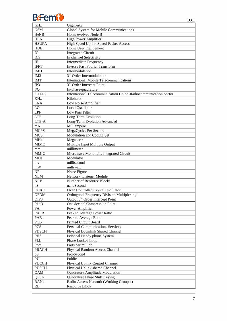
D3.1
7
GHz Gigahertz GSM Global System for Mobile Communications HeNB Home evolved Node B HPA High Power Amplifier HSUPA High Speed Uplink Speed Packet Access HUE Home User Equipement IC Integrated Circuit ICS In channel Selectivity IF Intermediate Frequency IFFT Inverse Fast Fourier Transform IMD Intermodulation IM3 3rd Order Intermodulation IMT International Mobile Telecommunications IP3 3rd Order Intercept Point I/Q In-phase/quadrature ITU-R International Telecommunication Union-Radiocommunication Sector KHz Kilohertz LNA Low Noise Amplifier LO Local Oscillator LPF Low Pass Filter LTE Long-Term Evolution LTE-A Long-Term Evolution Advanced mA Milliampere MCPS MegaCycles Per Second MCS Modulation and Coding Set MHz Megahertz MIMO Multiple Input Multiple Output mm millimeter MMIC Microwave Monolithic Integrated Circuit MOD Modulator ms millisecond mW milliwatt NF Noise Figure NLM Network Listener Module NRB Number of Resource Blocks nS nanoSecond OCXO Oven Controlled Crystal Oscillator OFDM Orthogonal Frequency Division Multiplexing OIP3 Output 3rd Order Intercept Point P1dB One decibel Compression Point PA Power Amplifier PAPR Peak to Average Power Ratio PAR Peak to Average Ratio PCB Printed Circuit Board PCS Personal Communications Services PDSCH Physical Downlink Shared Channel PHS Personal Handy phone System PLL Phase Locked Loop Ppm Parts per million PRACH Physical Random Access Channel pS PicoSecond PU Public PUCCH Physical Uplink Control Channel PUSCH Physical Uplink shared Channel QAM Quadrature Amplitude Modulation QPSK Quadrature Phase Shift Keying RAN4 Radio Access Network (Working Group 4) RB Resource Block
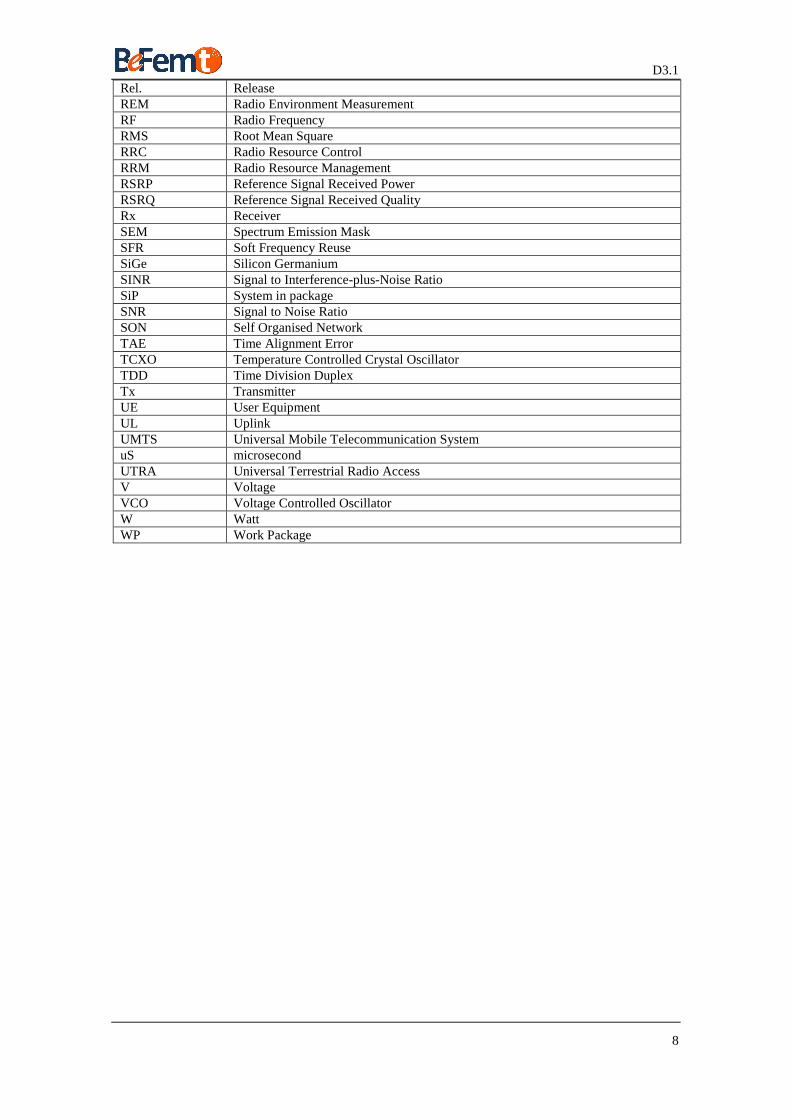
D3.1
8
Rel. Release REM Radio Environment Measurement RF Radio Frequency RMS Root Mean Square RRC Radio Resource Control RRM Radio Resource Management RSRP Reference Signal Received Power RSRQ Reference Signal Received Quality Rx Receiver SEM Spectrum Emission Mask SFR Soft Frequency Reuse SiGe Silicon Germanium SINR Signal to Interference-plus-Noise Ratio SiP System in package SNR Signal to Noise Ratio SON Self Organised Network TAE Time Alignment Error TCXO Temperature Controlled Crystal Oscillator TDD Time Division Duplex Tx Transmitter UE User Equipment UL Uplink UMTS Universal Mobile Telecommunication System uS microsecond UTRA Universal Terrestrial Radio Access V Voltage VCO Voltage Controlled Oscillator W Watt WP Work Package
D3.1
9
1. Introduction The increasing demand for data services on mobile phones puts continuous pressure on base station designs for more bandwidth and lower cost. Many factors influence the overall cost of installation and operation of additional base stations to serve these demands. Lower size and lower power electronics within a base station help to reduce the initial costs as well as the ongoing cost of real estate rental and electrical power consumption. Tiny picocells and femtocells extend the services to areas not covered by large macrocells. To make these gains effective, base stations designers need new components with very high levels of integration while maintaining a good level of performance.
Integration in the radio frequency (RF) portion of the radio is especially challenging because of the performance requirement. Over a decade ago, the typical base station architecture required several stages of low noise amplification, down conversion to an intermediate frequency (IF), filtering and further amplification. Higher performance mixers, amplifiers and higher dynamic range analog to digital converters (ADC’s) with higher sampling rates have enabled designers to eliminate down conversion stages to a single IF stage today.
In parallel, the handset radio has evolved to highly integrated baseband and transceiver integrated circuits (ICs), and integrated RF front-end modules (FEM). RF functional blocks between the transceiver and antenna include filtering, amplification and switching (with impedance matching incorporated between components where needed). The transceiver integrates the receiver ADC, the transmit DAC and the associated RF blocks. The FEM utilizes a system in package (SiP) technology to integrate various ICs and passives, including multimode filters and the RF switches for transmit and receive.
Among the previously mentioned types of base stations, BeFEMTO is focused on LTE-A femtocells. Femtocells are low coverage base stations intended for indoor or outdoor environments which are connected to the operator’s network through a broadband connection (such as DSL or cable). They present several advantages for both operators and users by improving the macrocell indoor coverage and boosting the spectral efficiency, allowing the operator to offload some traffic of the macrocell. These benefits lead to a growing and expected to turn massive deployment of this kind of devices, thus increasing the challenges which have to be faced. The constraint of compliance with the upcoming LTE-A standard gives and additional turn of the screw. This standard, with the use of more efficient modulations and above all the bandwidth extension to 100MHz (with carrier aggregation), puts a lot of pressure on the RF front-end hardware. Higher complex modulations mean stringent RF requirements, and higher bandwidth means higher number of transceivers needed to handle it (depending on the scenario), putting more obstacles to the module integration and its size reduction.
This deliverable deals with all of those issues, proposing novel solutions for RF front-end hardware and making sure that these solutions are valid for LTE-A. In order to fulfill these requirements, the research has been structured as in the following sections:
• Section 2 - RF front-end technical specifications: which identifies the technical specifications for the RF front-end hardware
• Section 3 – RF front-end architecture analysis: which analyzes and proposes the best option for the RF architecture
• Section 4 – Proposed RF front-end architecture solutions: which describes the proposed solutions, estimating their performance and checking its LTE-A compliance
D3.1
10
2. RF front-end technical specifications The Radio Access Specifications comprise the overall RF technical specification common to femtocells and particularized for LTE-A standalone femtocells. These specifications will define the requirements to be applied to the RF architecture design, and so to the RF component specifications. This section investigates the RF component specifications needed to meet the RF technical specifications in the femtocell, taken into account different architectures, scenarios and the advices given in 3GPP and in BeFEMTO WP2.
2.1 RF Technical Specifications
2.1.1 Problem Statement The technical RF requirements for LTE-A femtocell hardware are not defined in 3GPP [1] but several LTE (Rel. 8) parameters could be taken into account due to the fact that LTE-A must be LTE backward compatible. In [2], it is recommended that whenever appropriate, LTE-A RF requirements shall be based on the re-use of existing LTE Rel. 8 structure in a “building block” manner. However, not all component carriers (CCs) may necessarily be LTE Rel. 8 compatible [1].
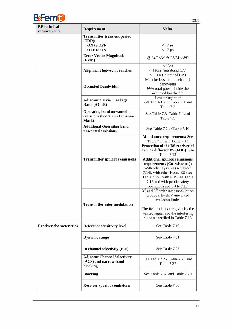
2.1.2 Specifications Overview The femtocell RF front-end has to be compliant with several requirements related to the main RF performance metrics. Thus, in [2] there are requirements defined for:
• Component carrier aggregation
• Transmitter characteristics
• Receiver characteristics
Next table summarises the RF technical requirements in the femtocell transceiver for LTE-A. A deeper description of each requirement is given in next subsections.
RF technical requirements
Requirement Value
Channel raster 100KHz
Channel Bandwidth (MHz) 1.4, 3, 5, 10, 15, 20
Additional Transmission Bandwidth configurations
102, 104, 106, 108, 110RBs
Extension Carrier Yes
Component carrier aggregation
Carrier spacing between contiguously aggregated CCs
Integer multiple of 300KHz
Frequency error ±0.25ppm
Local oscillator step size 300KHz
Local oscillator phase noise < 1ºrms (15KHz to 20MHz)
Maximum Output Power +10dBm
Power adjustment capability Yes
Transmitter characteristics
Transmitter OFF power (TDD) < -85dBm/MHz
D3.1
11
RF technical requirements
Requirement Value
Transmitter transient period (TDD): ON to OFF OFF to ON
< 17 µs < 17 µs
Error Vector Magnitude (EVM)
@ 64QAM � EVM < 8%
Alignment between branches < 65ns
< 130ns (intraband CA) < 1.3us (interband CA)
Occupied Bandwidth
Must be less that the channel bandwidth
99% total power inside the occupied bandwidth
Adjacent Carrier Leakage Ratio (ACLR)
Less stringent of -50dBm/MHz or Table 7.1 and
Table 7.2 Operating band unwanted emissions (Spectrum Emission Mask)
See Table 7.3, Table 7.4 and Table 7.5
Additional Operating band unwanted emissions
See Table 7.6 to Table 7.10
Transmitter spurious emissions
Mandatory requirements: See Table 7.11 and Table 7.12
Protection of the BS receiver of own or different BS (FDD): See
Table 7.13 Additional spurious emissions requirements (Co-existence): With other systems (see Table
7.14), with other Home BS (see Table 7.15), with PHS see Table
7.16 and with public safety operations see Table 7.17
Transmitter inter modulation
3rd and 5th order inter modulation products levels < unwanted
emission limits
The IM products are given by the wanted signal and the interfering signals specified in Table 7.18
Reference sensitivity level See Table 7.19
Dynamic range See Table 7.21
In channel selectivity (ICS) See Table 7.23
Adjacent Channel Selectivity (ACS) and narrow-band blocking
See Table 7.25, Table 7.26 and Table 7.27
Blocking See Table 7.28 and Table 7.29
Receiver characteristics
Receiver spurious emissions See Table 7.30
D3.1
12
RF technical requirements
Requirement Value
Receiver inter modulation See Table 7.31, Table 7.32 and
Table 7.33
Performance requirement See Table 7.34 to Table 7.39,
Table 7.45, Table 7.47
Local oscillator step size 300KHz
Table 2.1: Specifications overview
2.1.3 Component Carrier Aggregation Related to the component carrier aggregation in the femtocell, several requirements must be taken into account [4].
2.1.3.1 Channel raster
The channel raster is the frequency step that can be used in a communication device. In LTE-A the channel raster is 100 KHz, which means that the carrier centre frequency must be an integer of 100 KHz.
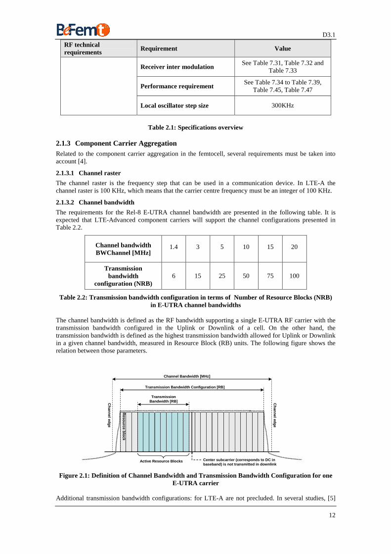
2.1.3.2 Channel bandwidth
The requirements for the Rel-8 E-UTRA channel bandwidth are presented in the following table. It is expected that LTE-Advanced component carriers will support the channel configurations presented in Table 2.2.
Channel bandwidth BWChannel [MHz]
1.4 3 5 10 15 20
Transmission bandwidth
configuration (NRB) 6 15 25 50 75 100
Table 2.2: Transmission bandwidth configuration in terms of Number of Resource Blocks (NRB) in E-UTRA channel bandwidths
The channel bandwidth is defined as the RF bandwidth supporting a single E-UTRA RF carrier with the transmission bandwidth configured in the Uplink or Downlink of a cell. On the other hand, the transmission bandwidth is defined as the highest transmission bandwidth allowed for Uplink or Downlink in a given channel bandwidth, measured in Resource Block (RB) units. The following figure shows the relation between those parameters.
TransmissionBandwidth [RB]
Transmission Bandwidth Configuration [RB]
Channel Bandwidth [MHz]
Center subcarrier (corresponds to DC in baseband) is not transmitted in downlink
Active Resource Blocks
Ch
ann
el edg
e
Ch
ann
el edg
e
Reso
urce b
lock
Figure 2.1: Definition of Channel Bandwidth and Transmission Bandwidth Configuration for one
E-UTRA carrier
Additional transmission bandwidth configurations: for LTE-A are not precluded. In several studies, [5]
D3.1
13
and [6], the usage of component carriers larger than 100RBs has been considered for contiguous carrier aggregation (up to 110RBs). The component carriers larger than 100RBs can be backward compatible to Rel-8 UEs as additional RBs are transparent and removed by the Rx filtering.
2.1.3.3 Extension carrier
An extension carrier is a carrier that is not backward compatible with Rel-8 and complies with the transmission bandwidth configuration of Table 2.2. In LTE-A not all the component carriers must be Rel-8 backward compatible.
2.1.3.4 Spacing between contiguously aggregated component carriers
In LTE-A, the spacing between centre frequencies of contiguously aggregated component carriers shall be a multiple of 300 KHz [4] in order to be compatible with the 100 KHz frequency raster of LTE and to preserve the subcarrier’s orthogonality (15 KHz spacing) at the same time [5].
2.1.4 Transmitter characteristics The most relevant femtocell transmitter requirements are enumerated below and are specified at each transmitter antenna connector. These requirements include key parameters in the RF architecture design as the frequency error, the local oscillator step size and phase noise, the EVM and the unwanted emissions in the femtocell. These latter requirements consist of:
1. Requirements for occupied bandwidth, 2. Out-of-band emissions (ACLR and Operating band unwanted emissions), 3. Transmitter spurious emissions.
2.1.4.1 Frequency error
The frequency error is the measure of the difference between the actual femtocell transmit frequency and the assigned one. This parameter is related to the reference clock accuracy. It has to be noted that the same source shall be used for RF frequency and data clock generation. For femtocells, the frequency error requirement is ±0.25ppm.
2.1.4.2 Local oscillator step size
It is the minimum step size for the transmitter local oscillator and it has to be the same than the spacing between contiguously aggregated component carriers, that is, 300 KHz.
2.1.4.3 Local oscillator phase noise
The phase noise is the frequency domain representation of fast, short-term and random fluctuations in the phase of a waveform (generated by a local oscillator), caused by time domain instabilities. The phase noise can have a significant effect on the overall EVM, so special attention should be put on the local oscillator design. For a 64QAM modulated OFDM signal, a total phase noise lower than 1ºrms from 15 KHz (symbol rate) to 20MHz (system bandwidth for a CC) is recommended [7].
2.1.4.4 Maximum Output Power
In the case of BeFEMTO transceiver the maximum output power is +10dBm over the full transmission bandwidth (BW).
2.1.4.5 Power adjustment capability
This requirement gives to the femtocell transmitter the availability of limiting the interference level.
2.1.4.6 Transmitter OFF power (TDD)
The transmitter OFF power is defined as the mean power measured over 70 µs filtered with a square filter of a bandwidth equal to the transmission bandwidth configuration of the Base Station (BS) centred on the assigned channel frequency during the transmitter OFF period.
For BS supporting intra-band contiguous CA, the transmitter OFF power is defined as the mean power measured over 70 µs filtered with a square filter of bandwidth equal to the Aggregated Channel Bandwidth centred on (Fedge_high+Fedge_low)/2 during the transmitter OFF period. Fedge_high (resp. Fedge_low) denote the frequency at the higher (resp. lower) edge of the aggregated channel band. The transmitter OFF power spectral density shall be less than -85dBm/MHz.
D3.1
14
2.1.4.7 Transmitter transient period (TDD)
This is the time period during which the transmitter is changing from the OFF to the ON period or vice versa. This period shall be shorter than 17µs for both transitions (OFF to ON and ON to OFF).
2.1.4.8 EVM (Error Vector Magnitude)
The error vector magnitude is a measure of the difference between the ideal and the measured symbols after the equalization. This difference is called the error vector. For all bandwidths, the EVM measurement shall be performed for each E-UTRA carrier over all allocated resource blocks and downlink subframes within 10ms measurement periods. The EVM value is calculated as the root mean square of the measured values. This parameter depends on the modulation scheme used. In BeFEMTO this will be 64QAM, so the EVM of each E-UTRA carrier on PDSCH shall be better than 8% [4]. This requirement can be extended in LTE-A on the basis of CC [2].
2.1.4.9 Time alignment between transmitter branches
This requirement applies to frame timing in TX diversity, MIMO transmission, carrier aggregation and their combinations. Frames of the LTE signals present at the BS transmitter antenna port(s) are not perfectly aligned in time. In relation to each other, the RF signals present at the BS transmitter antenna port(s) experience certain timing differences. For a specific set of signals/transmitter configuration/transmission mode, the time alignment error (TAE) is defined as the largest timing difference between any two signals.
For MIMO or TX diversity transmissions, at each carrier frequency, TAE shall not exceed 65 ns. For intra-band contiguous carrier aggregation, with or without MIMO or TX diversity, TAE shall not exceed 130 ns. For inter-band carrier aggregation, with or without MIMO or TX diversity, TAE shall not exceed 1.3 µs.
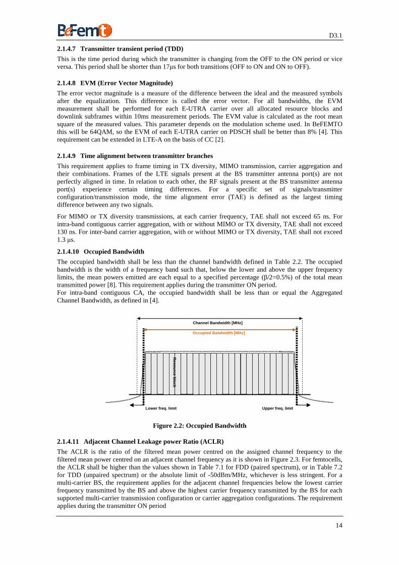
2.1.4.10 Occupied Bandwidth
The occupied bandwidth shall be less than the channel bandwidth defined in Table 2.2. The occupied bandwidth is the width of a frequency band such that, below the lower and above the upper frequency limits, the mean powers emitted are each equal to a specified percentage (β/2=0.5%) of the total mean transmitted power [8]. This requirement applies during the transmitter ON period. For intra-band contiguous CA, the occupied bandwidth shall be less than or equal the Aggregated Channel Bandwidth, as defined in [4].
Figure 2.2: Occupied Bandwidth
2.1.4.11 Adjacent Channel Leakage power Ratio (ACLR)
The ACLR is the ratio of the filtered mean power centred on the assigned channel frequency to the filtered mean power centred on an adjacent channel frequency as it is shown in Figure 2.3. For femtocells, the ACLR shall be higher than the values shown in Table 7.1 for FDD (paired spectrum), or in Table 7.2 for TDD (unpaired spectrum) or the absolute limit of -50dBm/MHz, whichever is less stringent. For a multi-carrier BS, the requirement applies for the adjacent channel frequencies below the lowest carrier frequency transmitted by the BS and above the highest carrier frequency transmitted by the BS for each supported multi-carrier transmission configuration or carrier aggregation configurations. The requirement applies during the transmitter ON period
Occupied Bandwidth [MHz]
Channel Bandwidth [MHz]
Lower freq. limit Upper freq. limit
Reso
urce b
lock
D3.1
15
ACLR limit ≥ 45dB -50dBm/MHz
Choose the less stringent
DOWNLINK OPERATING BAND
OPERATING BAND UNWANTED EMISSION LIMITS
10 MHz 10 MHz
CARRIER1st adjacent
E-UTRA carrier
2nd adjacent E-UTRA carrier
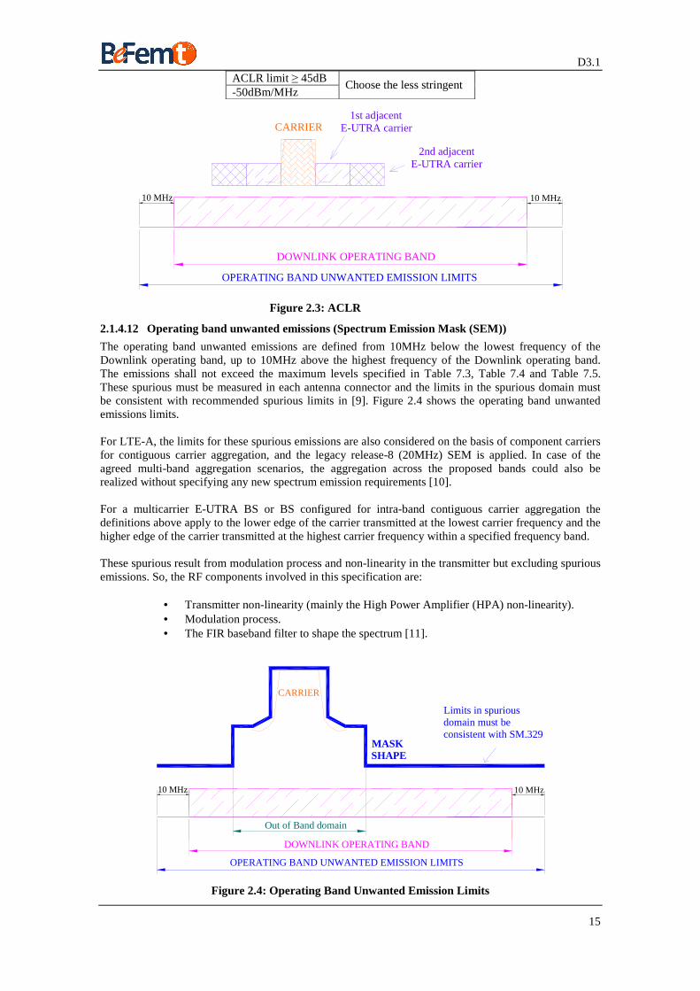
Figure 2.3: ACLR
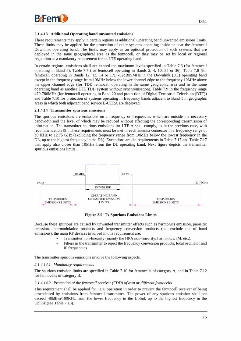
2.1.4.12 Operating band unwanted emissions (Spectrum Emission Mask (SEM))
The operating band unwanted emissions are defined from 10MHz below the lowest frequency of the Downlink operating band, up to 10MHz above the highest frequency of the Downlink operating band. The emissions shall not exceed the maximum levels specified in Table 7.3, Table 7.4 and Table 7.5. These spurious must be measured in each antenna connector and the limits in the spurious domain must be consistent with recommended spurious limits in [9]. Figure 2.4 shows the operating band unwanted emissions limits. For LTE-A, the limits for these spurious emissions are also considered on the basis of component carriers for contiguous carrier aggregation, and the legacy release-8 (20MHz) SEM is applied. In case of the agreed multi-band aggregation scenarios, the aggregation across the proposed bands could also be realized without specifying any new spectrum emission requirements [10]. For a multicarrier E-UTRA BS or BS configured for intra-band contiguous carrier aggregation the definitions above apply to the lower edge of the carrier transmitted at the lowest carrier frequency and the higher edge of the carrier transmitted at the highest carrier frequency within a specified frequency band. These spurious result from modulation process and non-linearity in the transmitter but excluding spurious emissions. So, the RF components involved in this specification are:
• Transmitter non-linearity (mainly the High Power Amplifier (HPA) non-linearity). • Modulation process. • The FIR baseband filter to shape the spectrum [11].
DOWNLINK OPERATING BAND
OPERATING BAND UNWANTED EMISSION LIMITS
10 MHz 10 MHz
CARRIER
Out of Band domain
MASK SHAPE
Limits in spurious domain must be consistent with SM.329
Figure 2.4: Operating Band Unwanted Emission Limits
D3.1
16
2.1.4.13 Additional Operating band unwanted emissions
These requirements may apply in certain regions as additional Operating band unwanted emissions limits. These limits may be applied for the protection of other systems operating inside or near the femtocell Downlink operating band. The limits may apply as an optional protection of such systems that are deployed in the same geographical area as the femtocell, or they may be set by local or regional regulation as a mandatory requirement for an LTE operating band.
In certain regions, emissions shall not exceed the maximum levels specified in Table 7.6 (for femtocell operating in Band 5), Table 7.7 (for femtocell operating in Bands 2, 4, 10, 35 or 36), Table 7.8 (for femtocell operating in Bands 12, 13, 14 or 17), -52dBm/MHz in the Downlink (DL) operating band except in the frequency range from 10MHz below the lower channel edge to the frequency 10MHz above the upper channel edge (for TDD femtocell operating in the same geographic area and in the same operating band as another LTE TDD system without synchronisation), Table 7.9 in the frequency range 470-780MHz (for femtocell operating in Band 20 and protection of Digital Terrestrial Television (DTT)) and Table 7.10 for protection of systems operating in frequency bands adjacent to Band 1 in geographic areas in which both adjacent band service E-UTRA are deployed.
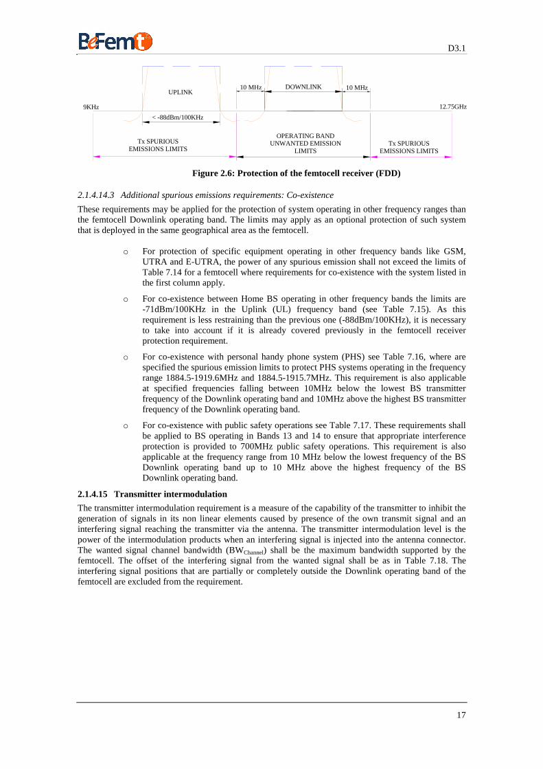
2.1.4.14 Transmitter spurious emissions
The spurious emissions are emissions on a frequency or frequencies which are outside the necessary bandwidth and the level of which may be reduced without affecting the corresponding transmission of information. The transmitter spurious emissions for LTE-A shall comply, as in the previous case, with recommendation [9]. These requirements must be met in each antenna connector in a frequency range of b9 KHz to 12.75 GHz (excluding the frequency range from 10MHz below the lowest frequency in the DL, up to the highest frequency in the DL). Exceptions are the requirements in Table 7.17 and Table 7.17 that apply also closer than 10MHz from the DL operating band. Next figure depicts the transmitter spurious emissions limits.
DOWNLINK
OPERATING BAND UNWANTED EMISSION
LIMITS
10 MHz 10 MHz
9KHz 12.75GHz
Tx SPURIOUS
EMISSIONS LIMITSTx SPURIOUS
EMISSIONS LIMITS
Figure 2.5: Tx Spurious Emissions Limits
Because these spurious are caused by unwanted transmitter effects such as harmonics emission, parasitic emission, intermodulation products and frequency conversion products (but exclude out of band emissions), the main RF devices involved in this requirement are:
• Transmitter non-linearity (mainly the HPA non-linearity: harmonics, IM, etc.). • Filters in the transmitter to reject the frequency conversion products, local oscillator and
IF frequencies. The transmitter spurious emissions involve the following aspects.
2.1.4.14.1 Mandatory requirements
The spurious emission limits are specified in Table 7.10 for femtocells of category A, and in Table 7.12 for femtocells of category B.
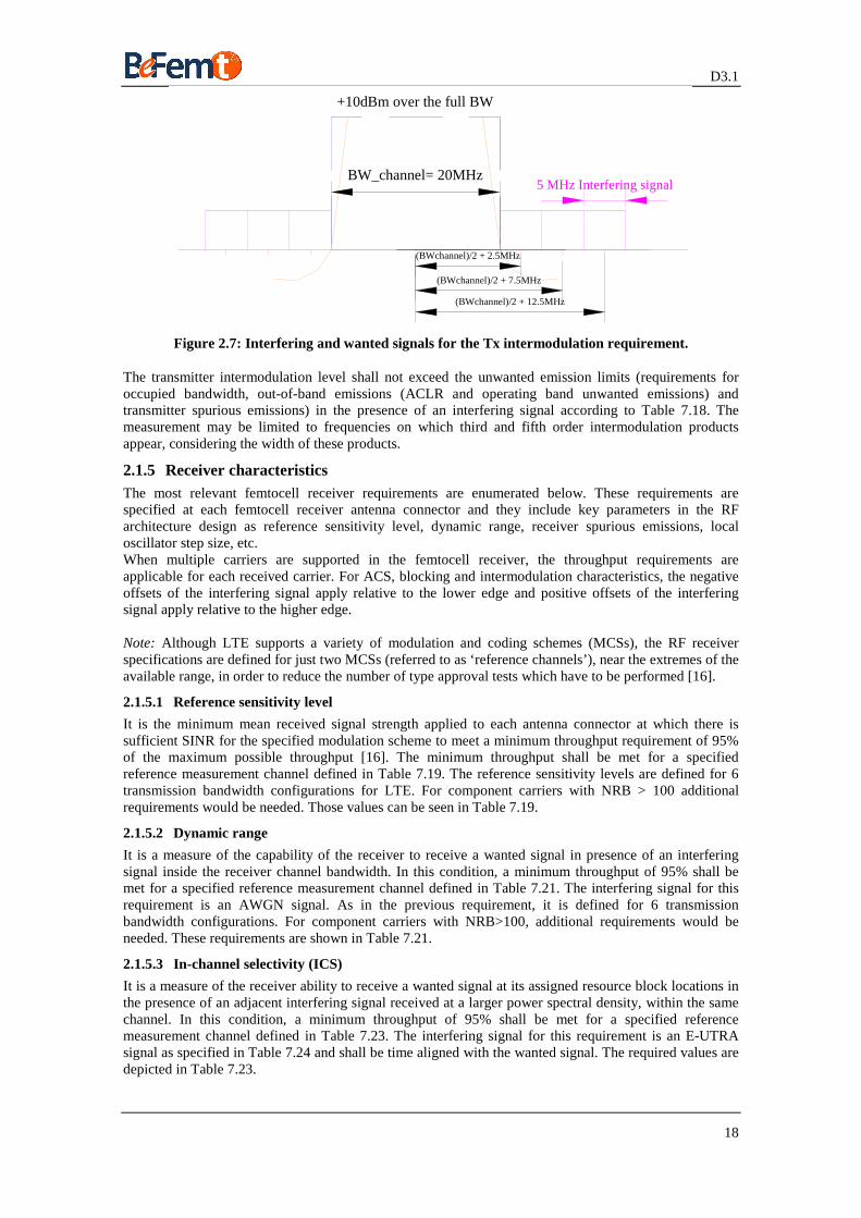
2.1.4.14.2 Protection of the femtocell receiver (FDD) of own or different femtocells
This requirement shall be applied for FDD operation in order to prevent the femtocell receiver of being desensitised by emissions from femtocell transmitter. The power of any spurious emission shall not exceed -88dBm/100KHz from the lower frequency in the Uplink up to the highest frequency in the Uplink (see Table 7.13).
D3.1
17
DOWNLINK
OPERATING BAND UNWANTED EMISSION
LIMITS
10 MHz 10 MHz
9KHz 12.75GHz
Tx SPURIOUS
EMISSIONS LIMITSTx SPURIOUS
EMISSIONS LIMITS
UPLINK
< -88dBm/100KHz
Figure 2.6: Protection of the femtocell receiver (FDD)
2.1.4.14.3 Additional spurious emissions requirements: Co-existence
These requirements may be applied for the protection of system operating in other frequency ranges than the femtocell Downlink operating band. The limits may apply as an optional protection of such system that is deployed in the same geographical area as the femtocell.
o For protection of specific equipment operating in other frequency bands like GSM, UTRA and E-UTRA, the power of any spurious emission shall not exceed the limits of Table 7.14 for a femtocell where requirements for co-existence with the system listed in the first column apply.
o For co-existence between Home BS operating in other frequency bands the limits are -71dBm/100KHz in the Uplink (UL) frequency band (see Table 7.15). As this requirement is less restraining than the previous one (-88dBm/100KHz), it is necessary to take into account if it is already covered previously in the femtocell receiver protection requirement.
o For co-existence with personal handy phone system (PHS) see Table 7.16, where are specified the spurious emission limits to protect PHS systems operating in the frequency range 1884.5-1919.6MHz and 1884.5-1915.7MHz. This requirement is also applicable at specified frequencies falling between 10MHz below the lowest BS transmitter frequency of the Downlink operating band and 10MHz above the highest BS transmitter frequency of the Downlink operating band.
o For co-existence with public safety operations see Table 7.17. These requirements shall be applied to BS operating in Bands 13 and 14 to ensure that appropriate interference protection is provided to 700MHz public safety operations. This requirement is also applicable at the frequency range from 10 MHz below the lowest frequency of the BS Downlink operating band up to 10 MHz above the highest frequency of the BS Downlink operating band.
2.1.4.15 Transmitter intermodulation
The transmitter intermodulation requirement is a measure of the capability of the transmitter to inhibit the generation of signals in its non linear elements caused by presence of the own transmit signal and an interfering signal reaching the transmitter via the antenna. The transmitter intermodulation level is the power of the intermodulation products when an interfering signal is injected into the antenna connector. The wanted signal channel bandwidth (BWChannel) shall be the maximum bandwidth supported by the femtocell. The offset of the interfering signal from the wanted signal shall be as in Table 7.18. The interfering signal positions that are partially or completely outside the Downlink operating band of the femtocell are excluded from the requirement.
D3.1
18
BW_channel= 20MHz5 MHz Interfering signal
+10dBm over the full BW
(BWchannel)/2 + 2.5MHz
(BWchannel)/2 + 7.5MHz
(BWchannel)/2 + 12.5MHz
Figure 2.7: Interfering and wanted signals for the Tx intermodulation requirement.
The transmitter intermodulation level shall not exceed the unwanted emission limits (requirements for occupied bandwidth, out-of-band emissions (ACLR and operating band unwanted emissions) and transmitter spurious emissions) in the presence of an interfering signal according to Table 7.18. The measurement may be limited to frequencies on which third and fifth order intermodulation products appear, considering the width of these products.
2.1.5 Receiver characteristics The most relevant femtocell receiver requirements are enumerated below. These requirements are specified at each femtocell receiver antenna connector and they include key parameters in the RF architecture design as reference sensitivity level, dynamic range, receiver spurious emissions, local oscillator step size, etc. When multiple carriers are supported in the femtocell receiver, the throughput requirements are applicable for each received carrier. For ACS, blocking and intermodulation characteristics, the negative offsets of the interfering signal apply relative to the lower edge and positive offsets of the interfering signal apply relative to the higher edge. Note: Although LTE supports a variety of modulation and coding schemes (MCSs), the RF receiver specifications are defined for just two MCSs (referred to as ‘reference channels’), near the extremes of the available range, in order to reduce the number of type approval tests which have to be performed [16].
2.1.5.1 Reference sensitivity level
It is the minimum mean received signal strength applied to each antenna connector at which there is sufficient SINR for the specified modulation scheme to meet a minimum throughput requirement of 95% of the maximum possible throughput [16]. The minimum throughput shall be met for a specified reference measurement channel defined in Table 7.19. The reference sensitivity levels are defined for 6 transmission bandwidth configurations for LTE. For component carriers with NRB > 100 additional requirements would be needed. Those values can be seen in Table 7.19.
2.1.5.2 Dynamic range
It is a measure of the capability of the receiver to receive a wanted signal in presence of an interfering signal inside the receiver channel bandwidth. In this condition, a minimum throughput of 95% shall be met for a specified reference measurement channel defined in Table 7.21. The interfering signal for this requirement is an AWGN signal. As in the previous requirement, it is defined for 6 transmission bandwidth configurations. For component carriers with NRB>100, additional requirements would be needed. These requirements are shown in Table 7.21.
2.1.5.3 In-channel selectivity (ICS)
It is a measure of the receiver ability to receive a wanted signal at its assigned resource block locations in the presence of an adjacent interfering signal received at a larger power spectral density, within the same channel. In this condition, a minimum throughput of 95% shall be met for a specified reference measurement channel defined in Table 7.23. The interfering signal for this requirement is an E-UTRA signal as specified in Table 7.24 and shall be time aligned with the wanted signal. The required values are depicted in Table 7.23.
D3.1
19
2.1.5.4 Adjacent Channel Selectivity (ACS) and narrow-band blocking
ACS is a measure of the receiver ability to receive a wanted signal at its assigned channel frequency in the presence of an adjacent channel signal with a specified centre frequency offset of the interfering signal to the band edge of a victim system. The interfering signal shall be an E-UTRA signal as specified in Table 7.24. The throughput shall be ≥ 95% of the maximum throughput of the reference measurement channel. For femtocells, the wanted and the interfering signal coupled to the BS antenna input are specified in Table 7.25 and Table 7.26 for narrowband blocking and in Table 7.27 for ACS. The reference measurement channel for the wanted signal is identified in Table 7.19 for each channel bandwidth.
2.1.5.5 Blocking
The blocking characteristics is a measure of the receiver ability to receive a wanted signal at its assigned channel in the presence of an unwanted interferer, which are either a 1.4MHz, 3MHz or 5MHz E-UTRA signal for in-band blocking or a continuous wave (CW) signal for out-of-band blocking. The interfering signal shall be an E-UTRA signal as specified in Table 7.24. The throughput shall be ≥ 95% of the maximum throughput of the reference measurement channel, with a wanted and an interfering signal coupled to BS antenna input using the parameters in Table 7.28 and Table 7.29. The reference measurement channel for the wanted signal is identified in Table 7.19 for each channel bandwidth.
2.1.5.6 Receiver spurious emissions
The receiver spurious emissions power is the power of emissions generated or amplified in the receiver that appears at the femtocell receiver antenna connector. The power of any spurious emission shall not exceed the levels presented in Table 7.30.
The requirements apply to:
• All femtocells with separate Rx and Tx antennas ports. For FDD case the test should be performed when Tx and Rx are ON (with Tx port terminated).
• In TDD case, with common Tx and Rx port, the requirement applies during the transmitter OFF period.
• For FDD femtocell with common Rx and Tx port, the “transmitter spurious emissions” specified in previous sections are valid.
In addition to the requirements in Table 7.30, the power of any spurious emission shall not exceed the levels specified for “protection of the femtocell receiver (FDD) of own or different femtocells” detailed in previous sections, and the “additional spurious emissions requirements for Co-existence” with other systems in the same geographical area (see previous sections).
2.1.5.7 Receiver intermodulation
Third and higher order mixing of the two interfering RF signals can produce an interfering signal in the band of the desired channel. Intermodulation response rejection is a measure of the capability of the receiver to receive a wanted signal on its assigned channel frequency in the presence of two interfering signals which have a specific frequency relationship to the wanted signal. Interfering signals shall be a CW signal and an E-UTRA signal as specified in Table 7.24. The throughput shall be ≥ 95% of the maximum throughput of the reference measurement channel, with a wanted signal at the assigned channel frequency and two interfering signals coupled to the femtocell antenna input, with the conditions specified in Table 7.31 and Table 7.32 for intermodulation performance and in Table 7.35 for narrowband intermodulation performance. The reference measurement channel for the wanted signal is identified in Table 7.19 for each channel.
2.1.5.8 Local oscillator step size
This is the same requirement than for the transmitter case, that is, 300 kHz.
2.1.6 Performance requirement For a LTE BS these demodulation requirements are specified for defined fixed reference channels (FRC) and propagation conditions. The requirements only apply for single carrier for the FRCs that are supported by the BS. In the case of carrier aggregation, the requirements are defined in terms of single carrier requirements.
For UL carrier aggregation within DC-HSUPA, demodulation performance requirements are derived from existing HSUPA requirements on a per-carrier basis, without the need of introducing additional Reference Channels. If the same approach is also utilized for CC aggregation in LTE-A, Rel-8
D3.1
20
demodulation performance requirements can be re-used. For NRB > 100, additional performance requirements would be needed. These requirements are specified for PUSCH, for PUCCH and for PRACH.
2.2 Requirements impact on RF
2.2.1 Problem Statement The RF specifications shall have a direct translation into the BeFEMTO femtocell. The RF architecture will be designed according to the parameters for LTE-A BeFEMTO femtocell and the RF technical specifications seen in the previous section. The RF architecture will have, whenever possible, a flexible configuration to cover the different component carrier aggregation scenarios.
2.2.2 RF specifications particularities in the BeFEMTO femtocell Most of the RF specifications are defined in the section 2.1, but other must be adapted to the particularities of BeFEMTO, for instance, a maximum power of 10dBm over any bandwidth in the desired signal. The following subsections will clarify the general RF specification in the case of the BeFEMTO femtocell.
2.2.2.1 Occupied Bandwidth
The occupied bandwidth specification applied to BeFEMTO femtocell is the following: for a CC of 20MHz with total maximum mean transmitted power of +10dBm (10mW), the occupied bandwidth shall be less than 20MHz, and the mean power emitted below the lower frequency limit is equal to 0.05mW or -13dBm (0.5% of 10dBm). The mean power emitted above the upper frequency limit is also equal to -13dBm. Several studies [6] include calculations in the occupied bandwidth with different number of RBs per CC (from 100RBs to 108RBs to improve the spectrum utilization for LTE-A).
2.2.2.2 Spectrum Emission Mask
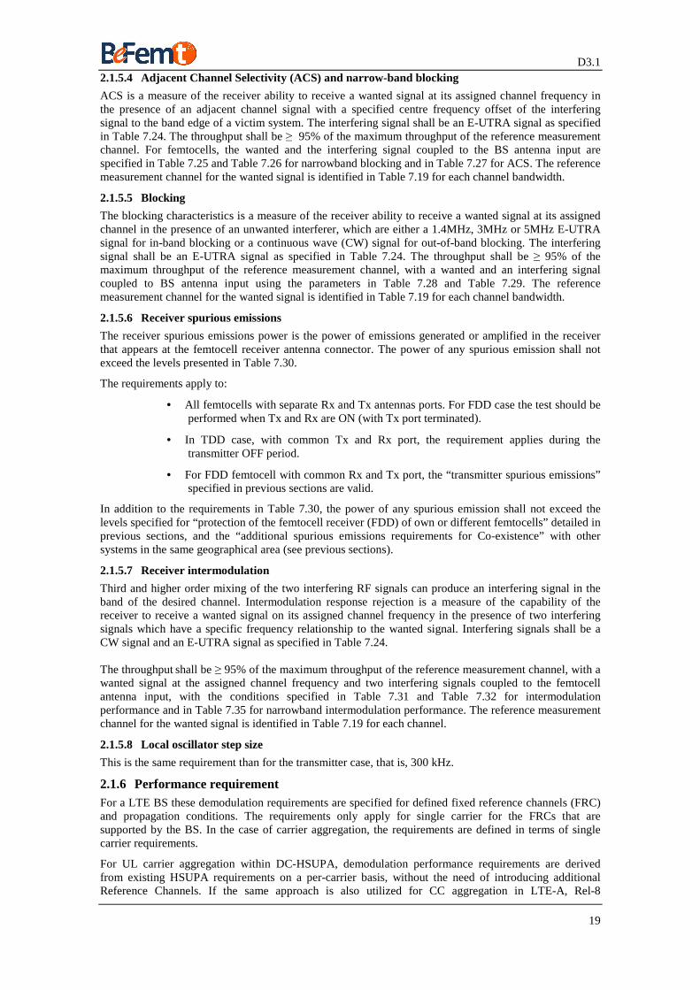
In order to have a clear vision about the SEM specification applied to BeFEMTO femtocell, a graph can be drawn with the requirement for SEM in dBm/100KHz vs. the frequency in MHz. For representation purpose, Band 40 (2.3-2.4GHz, TDD) is considered in the following but the rest of frequency bands are not excluded for the femtocell. In the case of using Band 40 for the Downlink in the femtocell (category A and category B), the emission mask shall satisfy the requirements from 2290MHz (2300MHz minus 10MHz) up to 2410MHz (2400Mhz plus 10MHz). The limits are defined in Table 7.3, Table 7.4 and Table 7.5, for 1.4MHz, 3.0MHz, and 5, 10, 15 and 20MHz respectively. In the next figure, the spurious emission mask of the femtocell in Band 40 can be seen, taking into account that the maximum power over each channel bandwidth is always +10dBm (according to the BeFEMTO goal).
D3.1
21
Figure 2.8: Spectrum Emission Mask in Band 40 (1.4, 3, 5, 10, 15 and 20MHz channel bandwidth) in the Home BS (category A and category B)
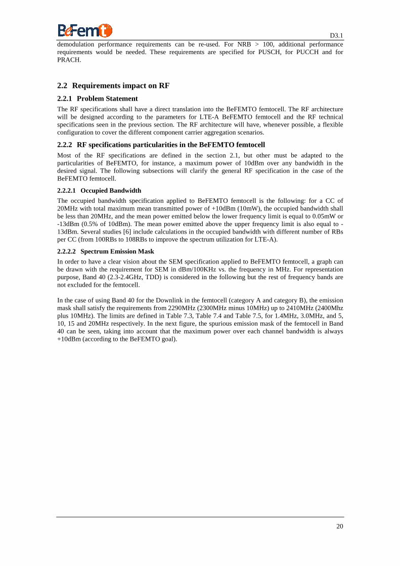
Following the LTE-A carrier aggregation, it is very interesting to perform a graphic representation of the spectrum emission mask over band 40 for one 20MHz CC, two 20MHz CC (40MHz channel BW), three 20MHz CC (60MHz channel bandwidth), four 20MHz CC (80MHz channel bandwidth) and five 20MHz CC (100MHz channel bandwidth). As in the previous case, the total power over each channel bandwidth is +10dBm.
Figure 2.9: Spectrum Emission Mask in Band 40 (20MHz (orange), 40MHz (blue), 60MHz (red), 80MHz (green) and 100 MHz (purple) channel bandwidth) in the femtocell.
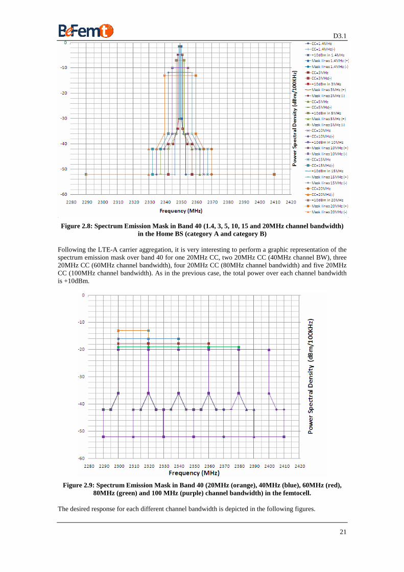
The desired response for each different channel bandwidth is depicted in the following figures.
D3.1
22
Figure 2.10: Spectrum Emission Mask in Band 40 (20MHz (left) and 40 MHz (right) channel bandwidth) in the femtocell.
Figure 2.11: Spectrum Emission Mask in Band 40 (60MHz (left) and 80 MHz (right) channel bandwidth) in the femtocell.
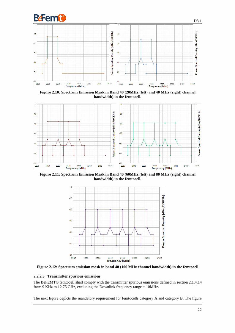
Figure 2.12: Spectrum emission mask in band 40 (100 MHz channel bandwidth) in the femtocell
2.2.2.3 Transmitter spurious emissions
The BeFEMTO femtocell shall comply with the transmitter spurious emissions defined in section 2.1.4.14 from 9 KHz to 12.75 GHz, excluding the Downlink frequency range ± 10MHz.
The next figure depicts the mandatory requirement for femtocells category A and category B. The figure
D3.1
23
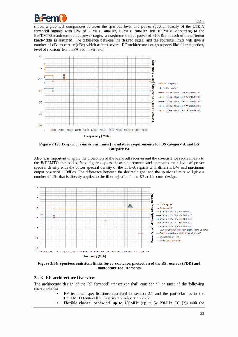
shows a graphical comparison between the spurious level and power spectral density of the LTE-A femtocell signals with BW of 20MHz, 40MHz, 60MHz, 80MHz and 100MHz. According to the BeFEMTO maximum output power target, a maximum output power of +10dBm in each of the different bandwidths is assumed. The difference between the desired signal and the spurious limits will give a number of dBs to carrier (dBc) which affects several RF architecture design aspects like filter rejection, level of spurious from HPA and mixer, etc.
Figure 2.13: Tx spurious emissions limits (mandatory requirements for BS category A and BS category B)
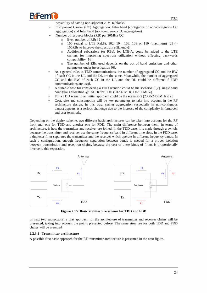
Also, it is important to apply the protection of the femtocell receiver and the co-existence requirements to the BeFEMTO femtocells. Next figure depicts these requirements and compares their level of power spectral density with the power spectral density of the LTE-A signals with different BW and maximum output power of +10dBm. The difference between the desired signal and the spurious limits will give a number of dBc that is directly applied to the filter rejection in the RF architecture design.
Figure 2.14: Spurious emissions limits for co-existence, protection of the BS receiver (FDD) and mandatory requirements
2.2.3 RF architecture Overview The architecture design of the RF femtocell transceiver shall consider all or most of the following characteristics:
• RF technical specifications described in section 2.1 and the particularities in the BeFEMTO femtocell summarized in subsection 2.2.2.
• Flexible channel bandwidth up to 100MHz (up to 5x 20MHz CC [2]) with the
D3.1
24
possibility of having non-adjacent 20MHz blocks. • Component Carrier (CC) Aggregation: Intra band (contiguous or non-contiguous CC
aggregation) and Inter band (non-contiguous CC aggregation). • Number of resource blocks (RB) per 20MHz CC:
o Even number of RBs [5] o 100 (equal to LTE Rel.8), 102, 104, 106, 108 or 110 (maximum) [2] (>
100RBs to improve the spectrum efficiency)] o Additional subcarriers (or RBs), for LTE-A, could be added to the LTE
carriers for improving spectrum utilization without affecting backwards compatibility [16].
o The number of RBs used depends on the out of band emissions and other parameters under investigation [6].
• As a general rule, in TDD communications, the number of aggregated CC and the BW of each CC in the UL and the DL are the same. Meanwhile, the number of aggregated CC and the BW of each CC in the UL and the DL could be different if FDD communications are used.
• A suitable base for considering a FDD scenario could be the scenario 1 [2], single band contiguous allocation @3.5GHz for FDD (UL: 40MHz, DL: 80MHZ)
• For a TDD scenario an initial approach could be the scenario 2 (2300-2400MHz) [2]. • Cost, size and consumption will be key parameters to take into account in the RF
architecture design. In this way, carrier aggregation (especially in non-contiguous bands) appears as a serious challenge due to the increase of the complexity in femtocell and user terminals.
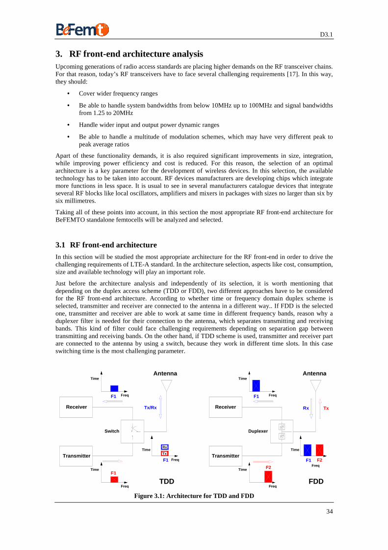
Depending on the duplex scheme, two different basic architectures can be taken into account for the RF front-end, one for TDD and another one for FDD. The main difference between them, in terms of architecture, is how the transmitter and receiver are joined. In the TDD case, it is made through a switch, because the transmitter and receiver use the same frequency band in different time slots. In the FDD case, a duplexer filter separates the transmitter and the receiver which operate in different frequency bands. In such a configuration, enough frequency separation between bands is needed for a proper isolation between transmission and reception chains, because the cost of these kinds of filters is proportionally inverse to this separation.
Rx
Tx
TDD
Antenna
Switch
Rx
Tx
FDD
Duplexer
Antenna
F1
F1
F1
F1
F2
F1 F2
Figure 2.15: Basic architecture scheme for TDD and FDD
In next two subsections, a first approach for the architecture of transmitter and receiver chains will be presented, taking into account the points presented before. The same structure for both TDD and FDD chains will be assumed.
2.2.3.1 Transmitter architecture
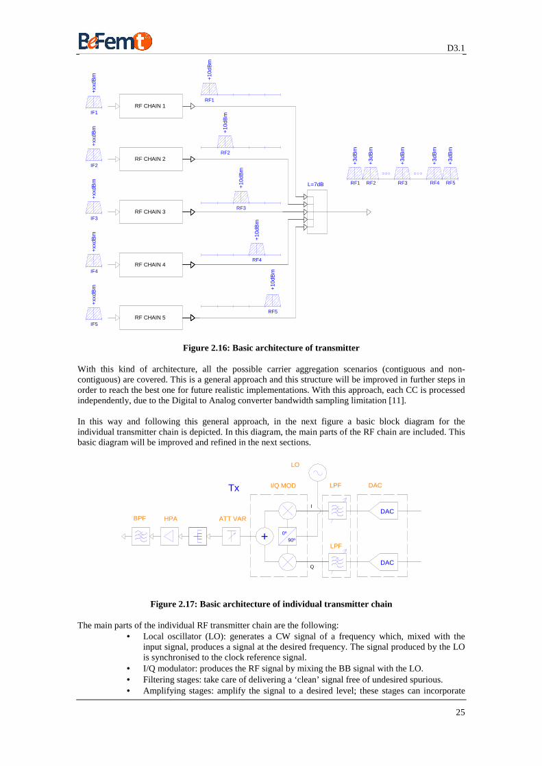
A possible first basic approach for the RF transmitter architecture is presented in the next figure.
D3.1
25
RF1
RF2
RF3
RF4
RF5
L=7dB+10
dBm
+10
dBm
+10
dBm
+10
dBm
+10d
Bm
IF1
+xxd
Bm
RF CHAIN 1
IF2
+xx
dBm
RF CHAIN 2
IF3
+xx
dBm
RF CHAIN 3
IF4
+xxd
Bm
RF CHAIN 4
IF5
+xx
dBm
RF CHAIN 5
RF1 RF2 RF3 RF4 RF5
+3d
Bm
+3d
Bm
+3d
Bm
+3d
Bm
+3d
Bm
Figure 2.16: Basic architecture of transmitter
With this kind of architecture, all the possible carrier aggregation scenarios (contiguous and non-contiguous) are covered. This is a general approach and this structure will be improved in further steps in order to reach the best one for future realistic implementations. With this approach, each CC is processed independently, due to the Digital to Analog converter bandwidth sampling limitation [11]. In this way and following this general approach, in the next figure a basic block diagram for the individual transmitter chain is depicted. In this diagram, the main parts of the RF chain are included. This basic diagram will be improved and refined in the next sections.
Q
HPA ATT VAR
90º+ 0º
I
Tx I/Q MOD
LO
BPF
LPF
DAC
LPF
DAC
DAC
Figure 2.17: Basic architecture of individual transmitter chain
The main parts of the individual RF transmitter chain are the following: • Local oscillator (LO): generates a CW signal of a frequency which, mixed with the
input signal, produces a signal at the desired frequency. The signal produced by the LO is synchronised to the clock reference signal.
• I/Q modulator: produces the RF signal by mixing the BB signal with the LO. • Filtering stages: take care of delivering a ‘clean’ signal free of undesired spurious. • Amplifying stages: amplify the signal to a desired level; these stages can incorporate
D3.1
26
gain control in order to add to the transmitter the power control ability. • High Power amplifier (HPA): this stage is in charge of delivery to the antenna the
desired output power for the component carrier signal, with a proper linearity characteristic.
2.2.3.2 Receiver architecture
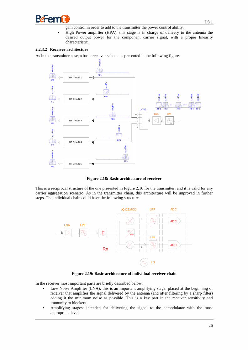
As in the transmitter case, a basic receiver scheme is presented in the following figure.
RF1
RF2
RF3
RF4
RF5
L=7dB-xxd
Bm
-xxd
Bm
-xxd
Bm
-xxd
Bm
-xxd
Bm
IF1
+xxd
Bm
RF CHAIN 1
IF2
+xxd
Bm
RF CHAIN 2
IF3
+xx
dBm
RF CHAIN 3
IF4
+xxd
Bm
RF CHAIN 4
IF5
+xxd
Bm
RF CHAIN 5
RF1 RF2 RF3 RF4 RF5
-xxd
Bm
-xxd
Bm
-xxd
Bm
-xxd
Bm
-xxd
Bm
LNA BPF
Figure 2.18: Basic architecture of receiver
This is a reciprocal structure of the one presented in Figure 2.16 for the transmitter, and it is valid for any carrier aggregation scenario. As in the transmitter chain, this architecture will be improved in further steps. The individual chain could have the following structure.
Rx
LPFLNA
0º90º
Q
I/Q DEMOD
I
LO
LPF
ADC
LPF
ADC
ADC
Figure 2.19: Basic architecture of individual receiver chain
In the receiver most important parts are briefly described below: • Low Noise Amplifier (LNA): this is an important amplifying stage, placed at the beginning of
receiver that amplifies the signal delivered by the antenna (and after filtering by a sharp filter) adding it the minimum noise as possible. This is a key part in the receiver sensitivity and immunity to blockers.
• Amplifying stages: intended for delivering the signal to the demodulator with the most appropriate level.
D3.1
27
• Filtering stages: several filtering stages are included in the receiver. Some (before the LNA and mixer) are for selecting the proper band avoiding undesired products mixings, and the other ones for the elimination of undesired spurious signals that could impair the signal demodulation. The baseband channel filter is typically a discrete lowpass design that provides both out-of-band blockers and broadband noise rejection before digitization.
• Local oscillator: generates a fixed stable signal which downconverts the RF signal to BB through the I/Q demodulator. The LO phase noise modulates nearby unfiltered blockers, adding noise to the wanted channel, so the demodulator local oscillator (LO) phase noise is a key parameter in the receiver.
• Quadrature demodulator: amplitude and phase errors can cause inband images or unwanted sideband energy, and strong in-band interfering signals may be adjacent to modulated carriers at the receiver sensitivity level. Maintaining adequate amplitude and phase balance through the baseband demodulation process is critical to good receiver performance.
• ADCs: As the unwanted blockers can reach the ADC without being attenuated, it is necessary to use high dynamic-range requirements for the receiver building blocks, especially the ADC. The receiver should have a high input 1-dB compression point, high-resolution ADCs, and some form of automatic gain control (AGC) to maintain blocker signal levels below the full-scale (FS) level of the ADC.
2.3 RF component specifications
2.3.1 Problem Statement After the definition of the overall RF technical specifications of the femtocell and the RF architecture alternatives, it is necessary to translate these requirements into a lower level of specifications: this will be the RF component specification. Once the specifications have been identified for the femtocell RF front-end, next problem to be solved is to know which component of transceiver is responsible of which requirement and how it can fulfill it taking into account the performance of available technology. The latter is an important issue, because the RF architecture must be oriented taking into consideration a future massive deployment.
2.3.2 RF component specifications Overview This section deals with the RF specifications at component level, which will determine the overall performance in the femtocell. These characteristics shall be in concordance with the RF technical specifications detailed in section 2.1. In this way, the next points will specify the requirements of the most important components of the RF architecture.
2.3.2.1 Clock
The frequency accuracy in the femtocell shall be ≤ ±0.25 ppm. Several crystal manufacturers have come up with various options to reduce the cost of the crystal local oscillator for femtocells. Thus, a temperature controlled oscillator (TCXO) is cheaper than an oven temperature controlled oscillator (OCXO). Hybrid devices are also available. However, there is higher risk in TCXO alternatives which can drift from their original reference frequency over a period of time. Those femtocells which are designed for enterprise applications use a tighter specification because they are not so price sensitive in comparison to residential femtocells.
2.3.2.2 Local Oscillator
The most characteristic parameter in a local oscillator is the phase noise performance. This characteristic (in receiver and transmitter) has direct contribution to the following RF specifications in the femtocell:
• EVM • Phase Noise and Jitter • Sensitivity • Blocking immunity
D3.1
28
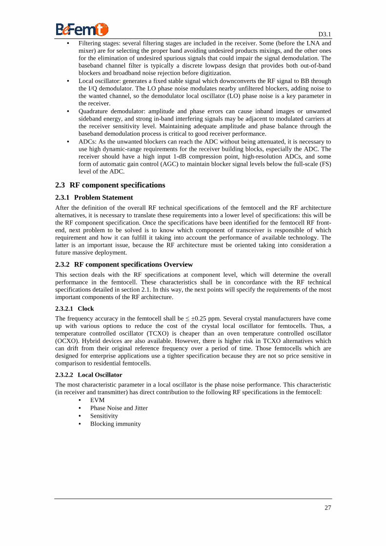
As is shown in the next figure, the better the local oscillator phase noise, the lower the EVM contribution [13]. For that reason, it is important to design a low cost local oscillator, while maintaining a low phase noise performance.
Figure 2.20: Local Oscillator Phase Noise vs. EVM
The local oscillator specifications shall be compliant with the RF technical specifications in the BeFEMTO femtocell (see section 2.1). The main LO specifications are:
Frequency error (fixed by the clock accuracy) ±0.25ppm
Local oscillator step size 300KHz
Local oscillator phase jitter < 1ºrms (15KHz to 20MHz)
Table 2.3: Local oscillator main requirements
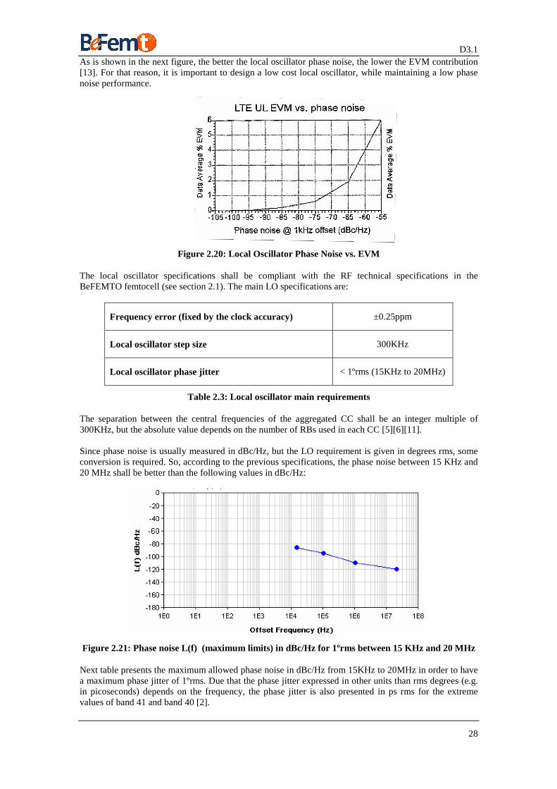
The separation between the central frequencies of the aggregated CC shall be an integer multiple of 300KHz, but the absolute value depends on the number of RBs used in each CC [5][6][11]. Since phase noise is usually measured in dBc/Hz, but the LO requirement is given in degrees rms, some conversion is required. So, according to the previous specifications, the phase noise between 15 KHz and 20 MHz shall be better than the following values in dBc/Hz:
Figure 2.21: Phase noise L(f) (maximum limits) in dBc/Hz for 1ºrms between 15 KHz and 20 MHz
Next table presents the maximum allowed phase noise in dBc/Hz from 15KHz to 20MHz in order to have a maximum phase jitter of 1ºrms. Due that the phase jitter expressed in other units than rms degrees (e.g. in picoseconds) depends on the frequency, the phase jitter is also presented in ps rms for the extreme values of band 41 and band 40 [2].
D3.1
29
)(º360(sec)_)(º_ HzfJitterPhasermsJitterPhase ⋅⋅=
Offset frequency
Phase Noise
(dBc/Hz)
Phase Jitter per
segment (º rms)
Phase Jitter per segment (ps rms)
@ 3600MHz
Phase Jitter per segment (ps rms)
@ 3400MHz
Phase Jitter per segment (ps rms)
@ 2400MHz
Phase Jitter per segment (ps rms)
@ 2300MHz
15KHz -86 100KHz -95 0.655 0.506 0.536 0.759 0.792 1MHz -110 0.5326 0.411 0.435 0.617 0.644 20MHz -120 0.5326 0.411 0.435 0.617 0.643 Total Phase Jitter (added as Root Sum-of-Squares)
1º 0.771 0.816 1.156 1.206
Table 2.4: Phase noise (maximum limits) for 1ºrms
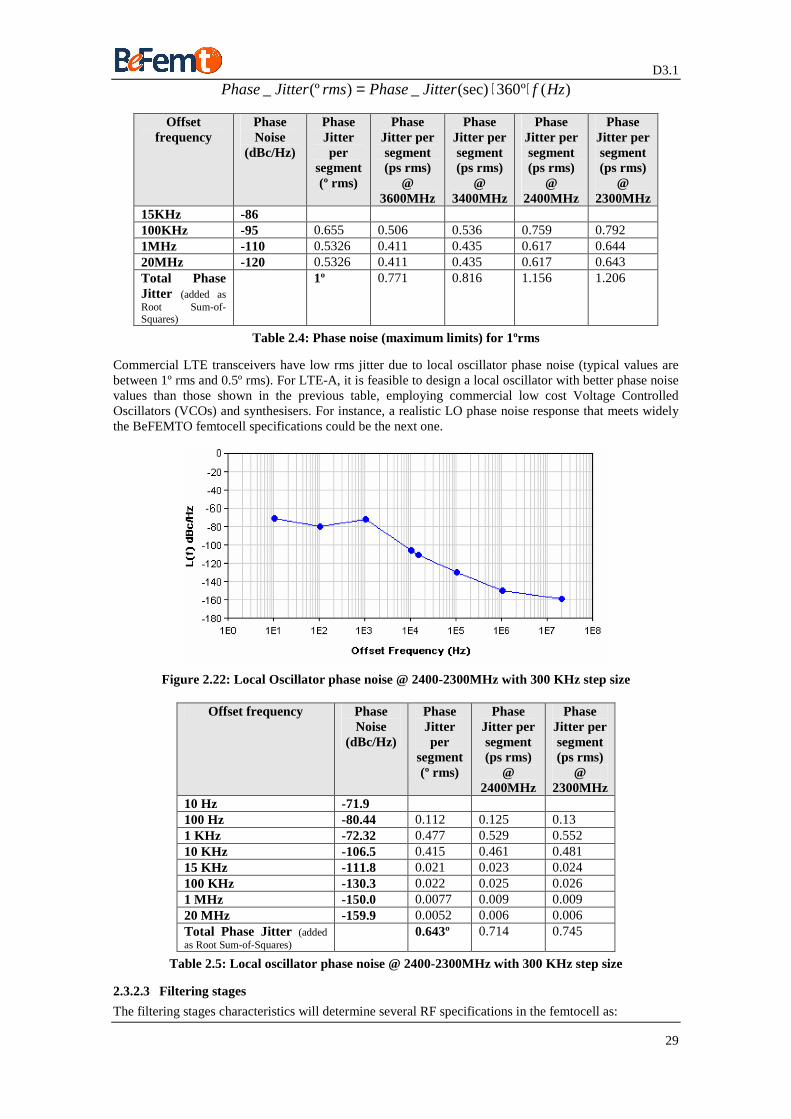
Commercial LTE transceivers have low rms jitter due to local oscillator phase noise (typical values are between 1º rms and 0.5º rms). For LTE-A, it is feasible to design a local oscillator with better phase noise values than those shown in the previous table, employing commercial low cost Voltage Controlled Oscillators (VCOs) and synthesisers. For instance, a realistic LO phase noise response that meets widely the BeFEMTO femtocell specifications could be the next one.
Figure 2.22: Local Oscillator phase noise @ 2400-2300MHz with 300 KHz step size
Offset frequency Phase Noise
(dBc/Hz)
Phase Jitter per
segment (º rms)
Phase Jitter per segment (ps rms)
@ 2400MHz
Phase Jitter per segment (ps rms)
@ 2300MHz
10 Hz -71.9 100 Hz -80.44 0.112 0.125 0.13 1 KHz -72.32 0.477 0.529 0.552 10 KHz -106.5 0.415 0.461 0.481 15 KHz -111.8 0.021 0.023 0.024 100 KHz -130.3 0.022 0.025 0.026 1 MHz -150.0 0.0077 0.009 0.009 20 MHz -159.9 0.0052 0.006 0.006 Total Phase Jitter (added as Root Sum-of-Squares)
0.643º 0.714 0.745
Table 2.5: Local oscillator phase noise @ 2400-2300MHz with 300 KHz step size
2.3.2.3 Filtering stages
The filtering stages characteristics will determine several RF specifications in the femtocell as:
D3.1
30
• LTE Rel.8 backward compatibility (different BW). • Channel raster and carrier aggregation centre frequency (the filter shall allow to pass the
frequencies of work in the femtocell). • Receiver noise figure (for the first filtering stages in the receiver) depending on the filter
losses. • Unwanted emissions: out of band spurious emissions (ACLR and SEM), transmitter
spurious emissions (filters in the transmitter to reject the frequency conversion products, local oscillator and IF frequencies) and receiver spurious emissions (filters in the receiver to reject the leakage in the connector antenna of frequency conversions, local oscillator and IF frequencies).
According to the graphical approach of the femtocell transmitter spurious emissions shown in section 2.2.2.3, it is of special interest to translate the difference of levels in the power spectral density to absolute values of rejection in dBc’s. A good level of reference in the spurious rejection could be the power spectral density of the LTE-A signal with +10dBm over 100MHz, this is -20dBm/100KHz. LTE-A desired signal Frequency range Maximum level
(dBm/100KHz) BeFEMTO femtocell rejection from LTE-A desired signal (dBc)
BeFEMTO femtocell with maximum output power of +10dBm, and maximum BW of 100MHz
One of the Downlink frequencies defined in [2]
-20 dBm/100KHz 0
Requirement Frequency range Mandatory for Femtocell Category A
9KHz to 150KHz 7 dBm/100KHz -27 dBc
150KHz to 30MHz -3 dBm/100KHz -17 dBc 30MHz to 1GHz -13 dBm/100KHz -7 dBc 1GHz to 12.75GHz -23 dBm/100KHz 3 dBc Mandatory for Femtocell Category B
9KHz to 150KHz -16 dBm/100KHz -4 dBc
150KHz to 30MHz -26 dBm/100KHz 6 dBc 30MHz to 1GHz -36 dBm/100KHz 16 dBc 1GHz to 12.75GHz -40 dBm/100KHz 20 dBc Protection of own receiver in the femtocell
Uplink frequency bands where the BeFEMTO femtocell receiver operates [2]
-88 dBm/100KHz 68 dBc
If BS = GSM900: DL(-57 dBm/100KHz) UL(-61 dBm/100KHz)
37 dBc 41 dBc
If BS = DCS1800: DL(-47 dBm/100KHz) UL(-61 dBm/100KHz)
27 dBc 41 dBc
If BS = PCS1900: DL(-47 dBm/100KHz) UL(-61 dBm/100KHz)
27 dBc 41 dBc
If BS = GSM850 or CDMA850:
DL(-57 dBm/100KHz) UL(-61 dBm/100KHz)
37 dBc 41 dBc
Co-existence with other BS
Uplink and Downlink frequency bands where operates the BS that must coexist with the BeFEMTO femtocell
If BS = FDD UTRA or E-UTRA in one band
from 1 to 20 [2]: DL(-62 dBm/100KHz) UL(-59 dBm/100KHz)
42 dBc 39 dBc
D3.1
31
LTE-A desired signal Frequency range Maximum level (dBm/100KHz)
BeFEMTO femtocell rejection from LTE-A desired signal (dBc)
If BS = TDD UTRA or E-UTRA in one band
from 33 to 40 [2]: DL=UL
(-62 dBm/100KHz)
42 dBc Co-existence with other femtocells
Uplink frequency band where operates the femtocell that must coexist with the BeFEMTO femtocell
-71 dBm/100KHz
51 dBc
1884.5-1915.7MHz -45.8 dBm/100KHz 25.8 dBc Co-existence with PHS 1884.5-1919.6MHz -45.8 dBm/100KHz 25.8 dBc 763-775MHz -33.9 dBm/100KHz 13.9 dBc 793-805MHz -33.9 dBm/100KHz 13.9 dBc 769-775MHz -33.9 dBm/100KHz 13.9 dBc
Co-existence of BeFEMTO femtocells that operates in band 13 or band 14 with 700MHz public safety operations
799-805MHz -33.9 dBm/100KHz 13.9 dBc
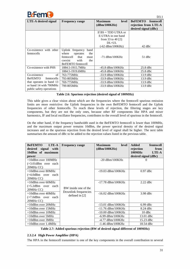
Table 2.6: Spurious rejection (desired signal of 100MHz)
This table gives a clear vision about which are the frequencies where the femtocell spurious emission limits are more restrictive: the Uplink frequencies in the own BeFEMTO femtocell and the Uplink frequencies of other femtocells. To reach these levels of rejection, the filtering stages are key components, but they are not the only ones, because other RF components like HPA and mixer harmonics, IF and local oscillator frequencies, contributes to the overall level of spurious in the femtocell. On the other hand, if the frequency bandwidth used in the BeFEMTO femtocell is lower than 100MHz, and the maximum output power remains 10dBm, the power spectral density of the desired signal increases and so the spurious rejection from the desired level of signal shall be higher. The next table summarises the amount of dBc to be added to the rejection values listed in the previous table. BeFEMTO LTE-A desired signal with 10dBm of maximum power
Frequency range Maximum level (dBm/100KHz)
Added femtocell rejection from 100MHz LTE-A desired signal (dBc)
+10dBm over 100MHz (+3.01dBm over each 20MHz CC)
-20 dBm/100KHz 0
+10dBm over 80MHz (+4.0dBm over each 20MHz CC)
-19.03 dBm/100KHz 0.97 dBc
+10dBm over 60MHz (+5.2dBm over each 20MHz CC)
-17.78 dBm/100KHz 2.22 dBc
+10dBm over 40MHz (+7.0dBm over each 20MHz CC)
-16.02 dBm/100KHz 3.98 dBc
+10dBm over 20MHz -13.01 dBm/100KHz 6.99 dBc +10dBm over 15MHz -11.76 dBm/100KHz 8.24 dBc +10dBm over 10MHz -10.00 dBm/100KHz 10 dBc +10dBm over 5MHz -6.99 dBm/100KHz 13.01 dBc +10dBm over 3MHz -4.77 dBm/100KHz 15.23 dBc +10dBm over 1.4MHz
BW inside one of the Downlink frequencies
defined in [2]
-1.46 dBm/100KHz 18.54 dBc
Table 2.7: Added spurious rejection (BW of desired signal different of 100MHz)
2.3.2.4 High Power Amplifier (HPA)
The HPA in the femtocell transmitter is one of the key components in the overall contribution to several
D3.1
32
RF parameters related with the components linearity: • Maximum output power • EVM • Occupied bandwidth • ACLR • Operating band unwanted emissions (SEM) • Transmitter spurious emissions (HPA harmonics and IM) • Transmitter intermodulation
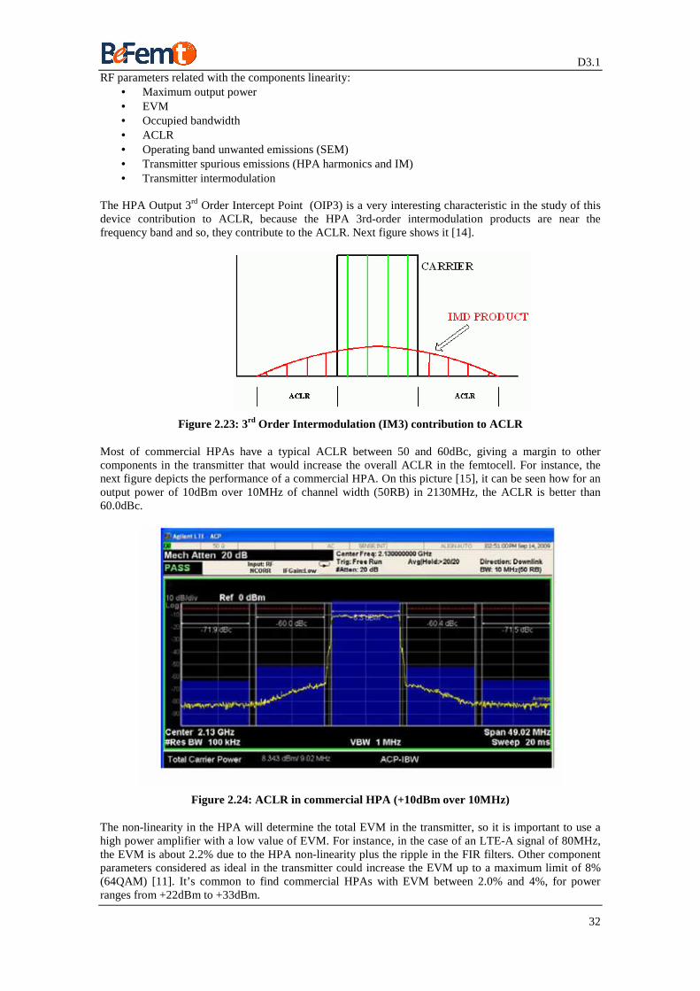
The HPA Output 3rd Order Intercept Point (OIP3) is a very interesting characteristic in the study of this device contribution to ACLR, because the HPA 3rd-order intermodulation products are near the frequency band and so, they contribute to the ACLR. Next figure shows it [14].
Figure 2.23: 3rd Order Intermodulation (IM3) contribution to ACLR
Most of commercial HPAs have a typical ACLR between 50 and 60dBc, giving a margin to other components in the transmitter that would increase the overall ACLR in the femtocell. For instance, the next figure depicts the performance of a commercial HPA. On this picture [15], it can be seen how for an output power of 10dBm over 10MHz of channel width (50RB) in 2130MHz, the ACLR is better than 60.0dBc.
Figure 2.24: ACLR in commercial HPA (+10dBm over 10MHz)
The non-linearity in the HPA will determine the total EVM in the transmitter, so it is important to use a high power amplifier with a low value of EVM. For instance, in the case of an LTE-A signal of 80MHz, the EVM is about 2.2% due to the HPA non-linearity plus the ripple in the FIR filters. Other component parameters considered as ideal in the transmitter could increase the EVM up to a maximum limit of 8% (64QAM) [11]. It’s common to find commercial HPAs with EVM between 2.0% and 4%, for power ranges from +22dBm to +33dBm.
D3.1
33
Other important parameter in the selection of the HPA is its 1dB compression point (P1dB). To select the proper value of P1dB, it is necessary to take into account the peak-to-average power ratio (PAPR), also called crest factor or peak-to-average ratio (PAR). The level of PAPR for OFDM signals should be 8.4dB according to [11]. Besides, it is recommended that the selected power amplifier has a reasonable amount of back-off from the 1dB compression point, for instance, at least 3dB above the signal PAPR. In the case of the maximum output power in the BeFEMTO femtocell that is +10dBm, the HPA should have a P1dB higher than +21.4dBm. Finally, and summarising, the criteria in the selection of the HPA shall take into account the following characteristics:
• Low cost • Low IM3 • Low EVM • High IP3 and P1dB • High harmonics suppression • High efficiency
2.3.2.5 Mixers
The mixer has a non negligible contribution in the RF specifications in terms of non-linearity in the transmitter and the receiver. Its performance will contribute to the following specifications in the femtocell:
• EVM • Occupied bandwidth • ACLR • Operating band unwanted emissions (SEM) • Transmitter and receiver spurious emissions (mixers harmonics and IM) • Transmitter and receiver intermodulation
It is recommended that the mixers included in the RF front-end have the following characteristics:
• Low cost • High IP3 • High harmonics suppression • High isolation between ports, minimizing the level of undesired frequencies like IF or RF
frequency and local oscillator frequency • High bandwidth • Low phase quadrature error (I/Q modulator) • Good Amplitude Balance performance
2.3.2.6 Low Noise Amplifier (LNA)
The LNA will determine a great number of RF specifications in the receiver part of the femtocell. The most important characteristics where it affects are:
• Receiver sensitivity • Receiver intermodulation • Receiver spurious emissions
The receiver sensitivity will be affected by the noise figure of the LNA (and the losses before it). In this way a lower noise figure in the receiver will improve the sensitivity and thus its ability to receive a signal at a lower power level. On the other hand, a LNA with enough P1dB will ensure lower levels of intermodulation in the receiver, meanwhile a good reverse isolation in the amplifier will help to reduce the level of the spurious emissions in the receiver antenna connector.
D3.1
34
3. RF front-end architecture analysis Upcoming generations of radio access standards are placing higher demands on the RF transceiver chains. For that reason, today’s RF transceivers have to face several challenging requirements [17]. In this way, they should:
• Cover wider frequency ranges
• Be able to handle system bandwidths from below 10MHz up to 100MHz and signal bandwidths from 1.25 to 20MHz
• Handle wider input and output power dynamic ranges
• Be able to handle a multitude of modulation schemes, which may have very different peak to peak average ratios
Apart of these functionality demands, it is also required significant improvements in size, integration, while improving power efficiency and cost is reduced. For this reason, the selection of an optimal architecture is a key parameter for the development of wireless devices. In this selection, the available technology has to be taken into account. RF devices manufacturers are developing chips which integrate more functions in less space. It is usual to see in several manufacturers catalogue devices that integrate several RF blocks like local oscillators, amplifiers and mixers in packages with sizes no larger than six by six millimetres.
Taking all of these points into account, in this section the most appropriate RF front-end architecture for BeFEMTO standalone femtocells will be analyzed and selected.
3.1 RF front-end architecture
In this section will be studied the most appropriate architecture for the RF front-end in order to drive the challenging requirements of LTE-A standard. In the architecture selection, aspects like cost, consumption, size and available technology will play an important role.
Just before the architecture analysis and independently of its selection, it is worth mentioning that depending on the duplex access scheme (TDD or FDD), two different approaches have to be considered for the RF front-end architecture. According to whether time or frequency domain duplex scheme is selected, transmitter and receiver are connected to the antenna in a different way.. If FDD is the selected one, transmitter and receiver are able to work at same time in different frequency bands, reason why a duplexer filter is needed for their connection to the antenna, which separates transmitting and receiving bands. This kind of filter could face challenging requirements depending on separation gap between transmitting and receiving bands. On the other hand, if TDD scheme is used, transmitter and receiver part are connected to the antenna by using a switch, because they work in different time slots. In this case switching time is the most challenging parameter.
Receiver
Transmitter
TDD
Antenna
Switch
FDD
Duplexer
Antenna
F1
F1
Tx/Rx
F1
F2
F1 F2
Rx
Tx
Rx Tx
F1
Receiver
Transmitter
Time
Freq
Time
Freq
Time
Freq
Time
Freq
Time
Freq
Time
Freq
Figure 3.1: Architecture for TDD and FDD
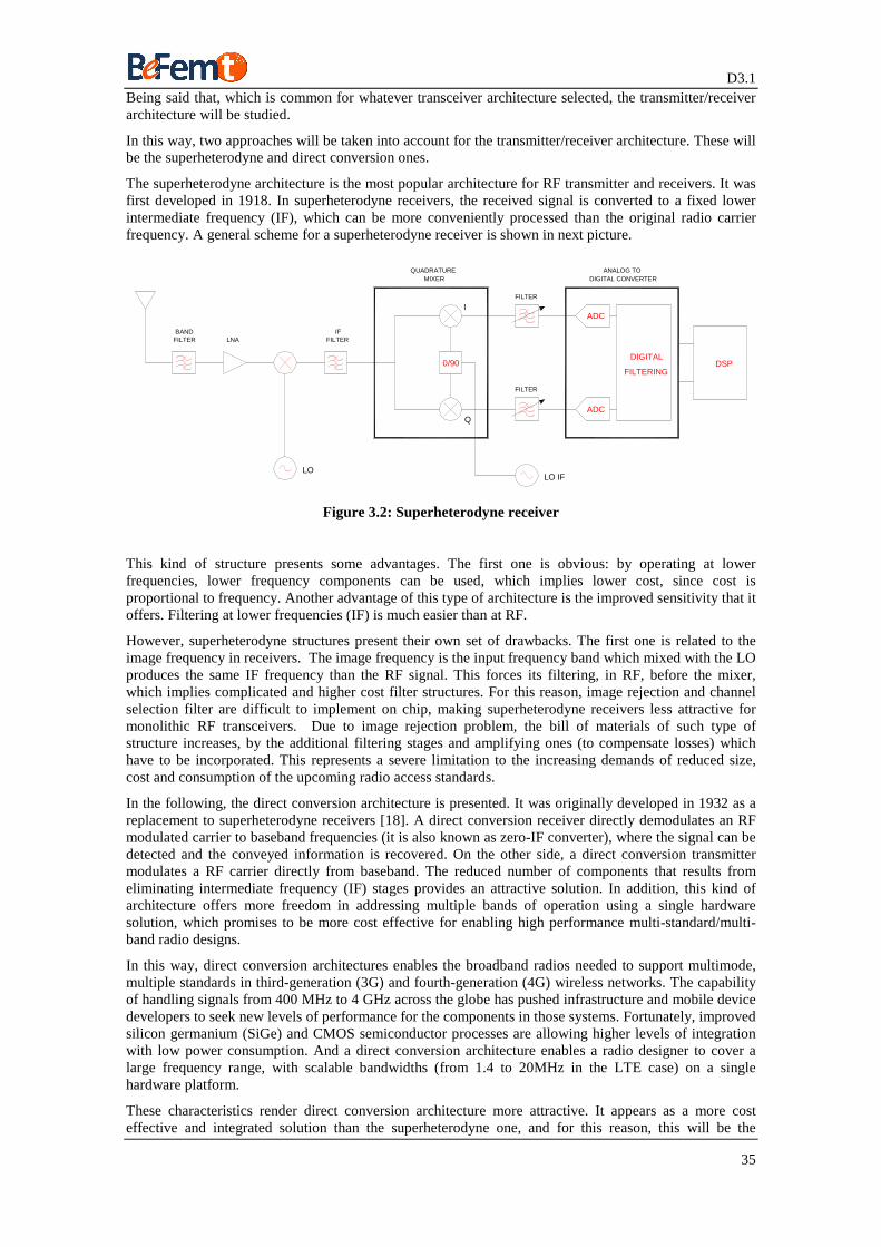
D3.1
35
Being said that, which is common for whatever transceiver architecture selected, the transmitter/receiver architecture will be studied.
In this way, two approaches will be taken into account for the transmitter/receiver architecture. These will be the superheterodyne and direct conversion ones.
The superheterodyne architecture is the most popular architecture for RF transmitter and receivers. It was first developed in 1918. In superheterodyne receivers, the received signal is converted to a fixed lower intermediate frequency (IF), which can be more conveniently processed than the original radio carrier frequency. A general scheme for a superheterodyne receiver is shown in next picture.
FILTER
FILTER
FILTERBAND
LO
0/90
Q
LNA FILTERIF
QUADRATUREMIXER
I
LO IF
ADC
DIGITAL
FILTERINGDSP
DIGITAL CONVERTERANALOG TO
ADC
Figure 3.2: Superheterodyne receiver
This kind of structure presents some advantages. The first one is obvious: by operating at lower frequencies, lower frequency components can be used, which implies lower cost, since cost is proportional to frequency. Another advantage of this type of architecture is the improved sensitivity that it offers. Filtering at lower frequencies (IF) is much easier than at RF.
However, superheterodyne structures present their own set of drawbacks. The first one is related to the image frequency in receivers. The image frequency is the input frequency band which mixed with the LO produces the same IF frequency than the RF signal. This forces its filtering, in RF, before the mixer, which implies complicated and higher cost filter structures. For this reason, image rejection and channel selection filter are difficult to implement on chip, making superheterodyne receivers less attractive for monolithic RF transceivers. Due to image rejection problem, the bill of materials of such type of structure increases, by the additional filtering stages and amplifying ones (to compensate losses) which have to be incorporated. This represents a severe limitation to the increasing demands of reduced size, cost and consumption of the upcoming radio access standards.
In the following, the direct conversion architecture is presented. It was originally developed in 1932 as a replacement to superheterodyne receivers [18]. A direct conversion receiver directly demodulates an RF modulated carrier to baseband frequencies (it is also known as zero-IF converter), where the signal can be detected and the conveyed information is recovered. On the other side, a direct conversion transmitter modulates a RF carrier directly from baseband. The reduced number of components that results from eliminating intermediate frequency (IF) stages provides an attractive solution. In addition, this kind of architecture offers more freedom in addressing multiple bands of operation using a single hardware solution, which promises to be more cost effective for enabling high performance multi-standard/multi-band radio designs.
In this way, direct conversion architectures enables the broadband radios needed to support multimode, multiple standards in third-generation (3G) and fourth-generation (4G) wireless networks. The capability of handling signals from 400 MHz to 4 GHz across the globe has pushed infrastructure and mobile device developers to seek new levels of performance for the components in those systems. Fortunately, improved silicon germanium (SiGe) and CMOS semiconductor processes are allowing higher levels of integration with low power consumption. And a direct conversion architecture enables a radio designer to cover a large frequency range, with scalable bandwidths (from 1.4 to 20MHz in the LTE case) on a single hardware platform.
These characteristics render direct conversion architecture more attractive. It appears as a more cost effective and integrated solution than the superheterodyne one, and for this reason, this will be the
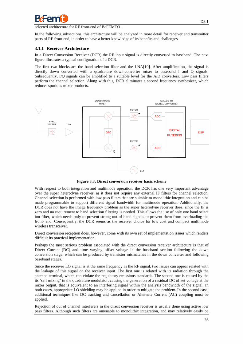
D3.1
36
selected architecture for RF front-end of BeFEMTO.
In the following subsections, this architecture will be analyzed in more detail for receiver and transmitter parts of RF front-end, in order to have a better knowledge of its benefits and challenges.
3.1.1 Receiver Architecture In a Direct Conversion Receiver (DCR) the RF input signal is directly converted to baseband. The next figure illustrates a typical configuration of a DCR.
The first two blocks are the band selection filter and the LNA[19]. After amplification, the signal is directly down converted with a quadrature down-converter mixer to baseband I and Q signals. Subsequently, I/Q signals can be amplified to a suitable level for the A/D converters. Low pass filters perform the channel selection. Along with this, DCR eliminates a second frequency synthesizer, which reduces spurious mixer products.
I
FILTER
LO
ADC
Q
0/90
BANDFILTER LNA
FILTER
QUADRATUREMIXER
ADC
DIGITAL
FILTERING
DIGITAL CONVERTERANALOG TO
DSP
Figure 3.3: Direct conversion receiver basic scheme
With respect to both integration and multimode operation, the DCR has one very important advantage over the super heterodyne receiver, as it does not require any external IF filters for channel selection. Channel selection is performed with low pass filters that are suitable to monolithic integration and can be made programmable to support different signal bandwidth for multimode operation. Additionally, the DCR does not have the image frequency problem as the super heterodyne receiver does, since the IF is zero and no requirement to band selection filtering is needed. This allows the use of only one band select ion filter, which needs only to prevent strong out of band signals to prevent them from overloading the front- end. Consequently, the DCR seems as the receiver choice for low cost and compact multimode wireless transceiver.
Direct conversion reception does, however, come with its own set of implementation issues which renders difficult its practical implementation.
Perhaps the most serious problem associated with the direct conversion receiver architecture is that of Direct Current (DC) and time varying offset voltage in the baseband section following the down conversion stage, which can be produced by transistor mismatches in the down converter and following baseband stages.
Since the receiver LO signal is at the same frequency as the RF signal, two issues can appear related with the leakage of this signal on the receiver input. The first one is related with its radiation through the antenna terminal, which can violate the regulatory emissions standards. The second one is caused by the its ‘self mixing’ in the quadrature modulator, causing the generation of a residual DC offset voltage at the mixer output, that is equivalent to an interfering signal within the analysis bandwidth of the signal. In both cases, appropriate LO shielding may be applied in order to mitigate the problem. In the second case, additional techniques like DC tracking and cancellation or Alternate Current (AC) coupling must be applied.
Rejection of out of channel interferers in the direct conversion receiver is usually done using active low pass filters. Although such filters are amenable to monolithic integration, and may relatively easily be
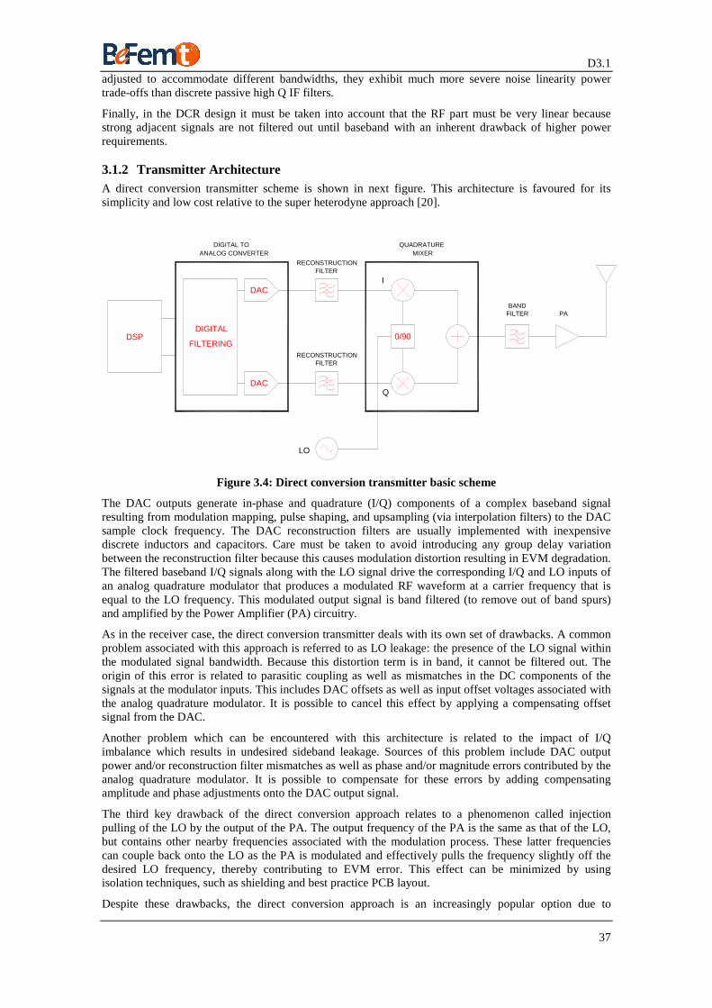
D3.1
37
adjusted to accommodate different bandwidths, they exhibit much more severe noise linearity power trade-offs than discrete passive high Q IF filters.
Finally, in the DCR design it must be taken into account that the RF part must be very linear because strong adjacent signals are not filtered out until baseband with an inherent drawback of higher power requirements.
3.1.2 Transmitter Architecture A direct conversion transmitter scheme is shown in next figure. This architecture is favoured for its simplicity and low cost relative to the super heterodyne approach [20].
DAC
DAC
DIGITAL
FILTERING
RECONSTRUCTIONFILTER
FILTERRECONSTRUCTION
0/90
LO
QUADRATUREMIXER
DIGITAL TOANALOG CONVERTER
DSP
I
Q
BANDFILTER PA
Figure 3.4: Direct conversion transmitter basic scheme
The DAC outputs generate in-phase and quadrature (I/Q) components of a complex baseband signal resulting from modulation mapping, pulse shaping, and upsampling (via interpolation filters) to the DAC sample clock frequency. The DAC reconstruction filters are usually implemented with inexpensive discrete inductors and capacitors. Care must be taken to avoid introducing any group delay variation between the reconstruction filter because this causes modulation distortion resulting in EVM degradation. The filtered baseband I/Q signals along with the LO signal drive the corresponding I/Q and LO inputs of an analog quadrature modulator that produces a modulated RF waveform at a carrier frequency that is equal to the LO frequency. This modulated output signal is band filtered (to remove out of band spurs) and amplified by the Power Amplifier (PA) circuitry.
As in the receiver case, the direct conversion transmitter deals with its own set of drawbacks. A common problem associated with this approach is referred to as LO leakage: the presence of the LO signal within the modulated signal bandwidth. Because this distortion term is in band, it cannot be filtered out. The origin of this error is related to parasitic coupling as well as mismatches in the DC components of the signals at the modulator inputs. This includes DAC offsets as well as input offset voltages associated with the analog quadrature modulator. It is possible to cancel this effect by applying a compensating offset signal from the DAC.
Another problem which can be encountered with this architecture is related to the impact of I/Q imbalance which results in undesired sideband leakage. Sources of this problem include DAC output power and/or reconstruction filter mismatches as well as phase and/or magnitude errors contributed by the analog quadrature modulator. It is possible to compensate for these errors by adding compensating amplitude and phase adjustments onto the DAC output signal.
The third key drawback of the direct conversion approach relates to a phenomenon called injection pulling of the LO by the output of the PA. The output frequency of the PA is the same as that of the LO, but contains other nearby frequencies associated with the modulation process. These latter frequencies can couple back onto the LO as the PA is modulated and effectively pulls the frequency slightly off the desired LO frequency, thereby contributing to EVM error. This effect can be minimized by using isolation techniques, such as shielding and best practice PCB layout.
Despite these drawbacks, the direct conversion approach is an increasingly popular option due to
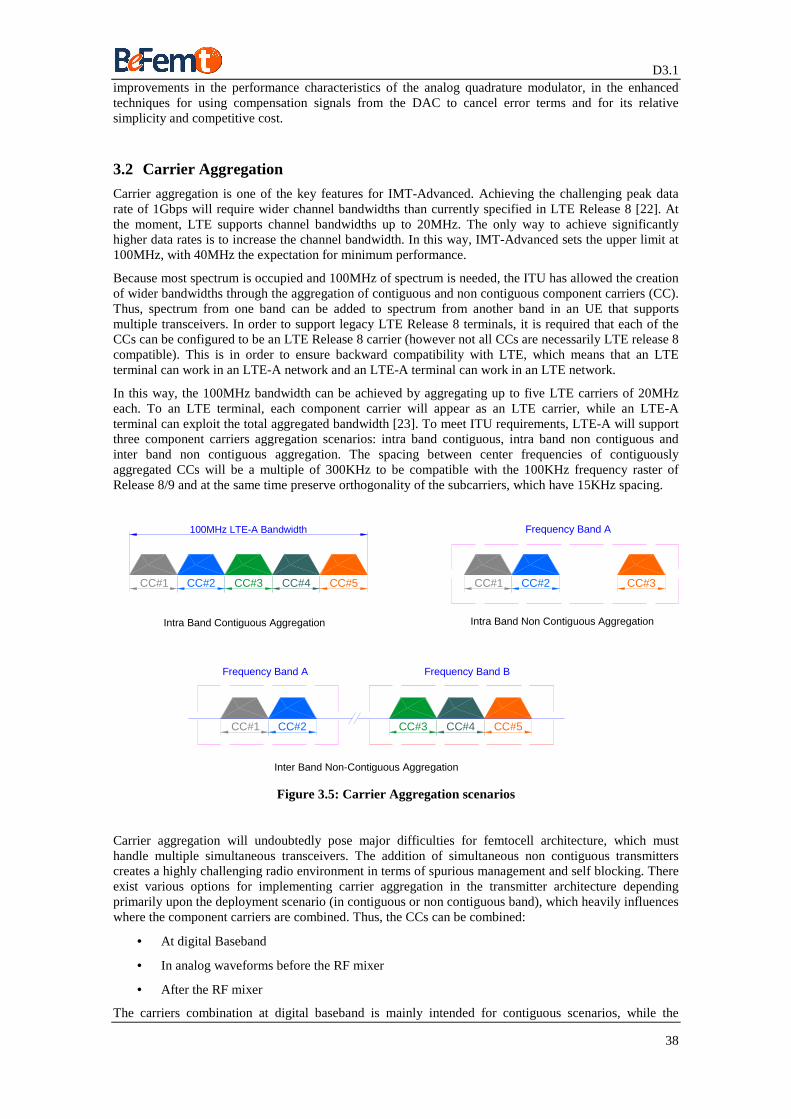
D3.1
38
improvements in the performance characteristics of the analog quadrature modulator, in the enhanced techniques for using compensation signals from the DAC to cancel error terms and for its relative simplicity and competitive cost.
3.2 Carrier Aggregation
Carrier aggregation is one of the key features for IMT-Advanced. Achieving the challenging peak data rate of 1Gbps will require wider channel bandwidths than currently specified in LTE Release 8 [22]. At the moment, LTE supports channel bandwidths up to 20MHz. The only way to achieve significantly higher data rates is to increase the channel bandwidth. In this way, IMT-Advanced sets the upper limit at 100MHz, with 40MHz the expectation for minimum performance.
Because most spectrum is occupied and 100MHz of spectrum is needed, the ITU has allowed the creation of wider bandwidths through the aggregation of contiguous and non contiguous component carriers (CC). Thus, spectrum from one band can be added to spectrum from another band in an UE that supports multiple transceivers. In order to support legacy LTE Release 8 terminals, it is required that each of the CCs can be configured to be an LTE Release 8 carrier (however not all CCs are necessarily LTE release 8 compatible). This is in order to ensure backward compatibility with LTE, which means that an LTE terminal can work in an LTE-A network and an LTE-A terminal can work in an LTE network.
In this way, the 100MHz bandwidth can be achieved by aggregating up to five LTE carriers of 20MHz each. To an LTE terminal, each component carrier will appear as an LTE carrier, while an LTE-A terminal can exploit the total aggregated bandwidth [23]. To meet ITU requirements, LTE-A will support three component carriers aggregation scenarios: intra band contiguous, intra band non contiguous and inter band non contiguous aggregation. The spacing between center frequencies of contiguously aggregated CCs will be a multiple of 300KHz to be compatible with the 100KHz frequency raster of Release 8/9 and at the same time preserve orthogonality of the subcarriers, which have 15KHz spacing.
CC#1 CC#4CC#2
Frequency Band A
CC#3 CC#5
CC#2CC#1 CC#4CC#3 CC#5
Frequency Band B
Inter Band Non-Contiguous Aggregation
Intra Band Contiguous Aggregation
100MHz LTE-A Bandwidth
Intra Band Non Contiguous Aggregation
CC#2CC#1 CC#3
Frequency Band A
Figure 3.5: Carrier Aggregation scenarios
Carrier aggregation will undoubtedly pose major difficulties for femtocell architecture, which must handle multiple simultaneous transceivers. The addition of simultaneous non contiguous transmitters creates a highly challenging radio environment in terms of spurious management and self blocking. There exist various options for implementing carrier aggregation in the transmitter architecture depending primarily upon the deployment scenario (in contiguous or non contiguous band), which heavily influences where the component carriers are combined. Thus, the CCs can be combined:
• At digital Baseband
• In analog waveforms before the RF mixer
• After the RF mixer
The carriers combination at digital baseband is mainly intended for contiguous scenarios, while the
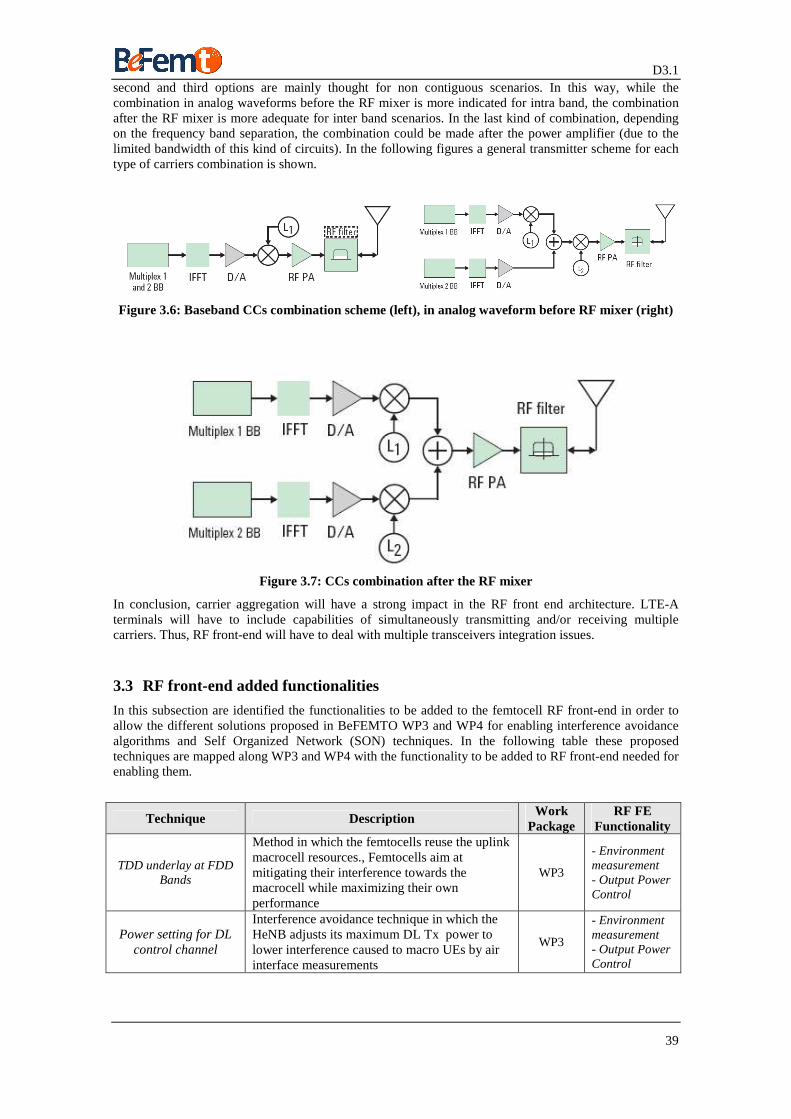
D3.1
39
second and third options are mainly thought for non contiguous scenarios. In this way, while the combination in analog waveforms before the RF mixer is more indicated for intra band, the combination after the RF mixer is more adequate for inter band scenarios. In the last kind of combination, depending on the frequency band separation, the combination could be made after the power amplifier (due to the limited bandwidth of this kind of circuits). In the following figures a general transmitter scheme for each type of carriers combination is shown.
Figure 3.6: Baseband CCs combination scheme (left), in analog waveform before RF mixer (right)
Figure 3.7: CCs combination after the RF mixer
In conclusion, carrier aggregation will have a strong impact in the RF front end architecture. LTE-A terminals will have to include capabilities of simultaneously transmitting and/or receiving multiple carriers. Thus, RF front-end will have to deal with multiple transceivers integration issues.
3.3 RF front-end added functionalities
In this subsection are identified the functionalities to be added to the femtocell RF front-end in order to allow the different solutions proposed in BeFEMTO WP3 and WP4 for enabling interference avoidance algorithms and Self Organized Network (SON) techniques. In the following table these proposed techniques are mapped along WP3 and WP4 with the functionality to be added to RF front-end needed for enabling them.
Technique Description Work
Package RF FE
Functionality
TDD underlay at FDD Bands
Method in which the femtocells reuse the uplink macrocell resources., Femtocells aim at mitigating their interference towards the macrocell while maximizing their own performance
WP3
- Environment measurement - Output Power Control
Power setting for DL control channel
Interference avoidance technique in which the HeNB adjusts its maximum DL Tx power to lower interference caused to macro UEs by air interface measurements
WP3
- Environment measurement - Output Power Control
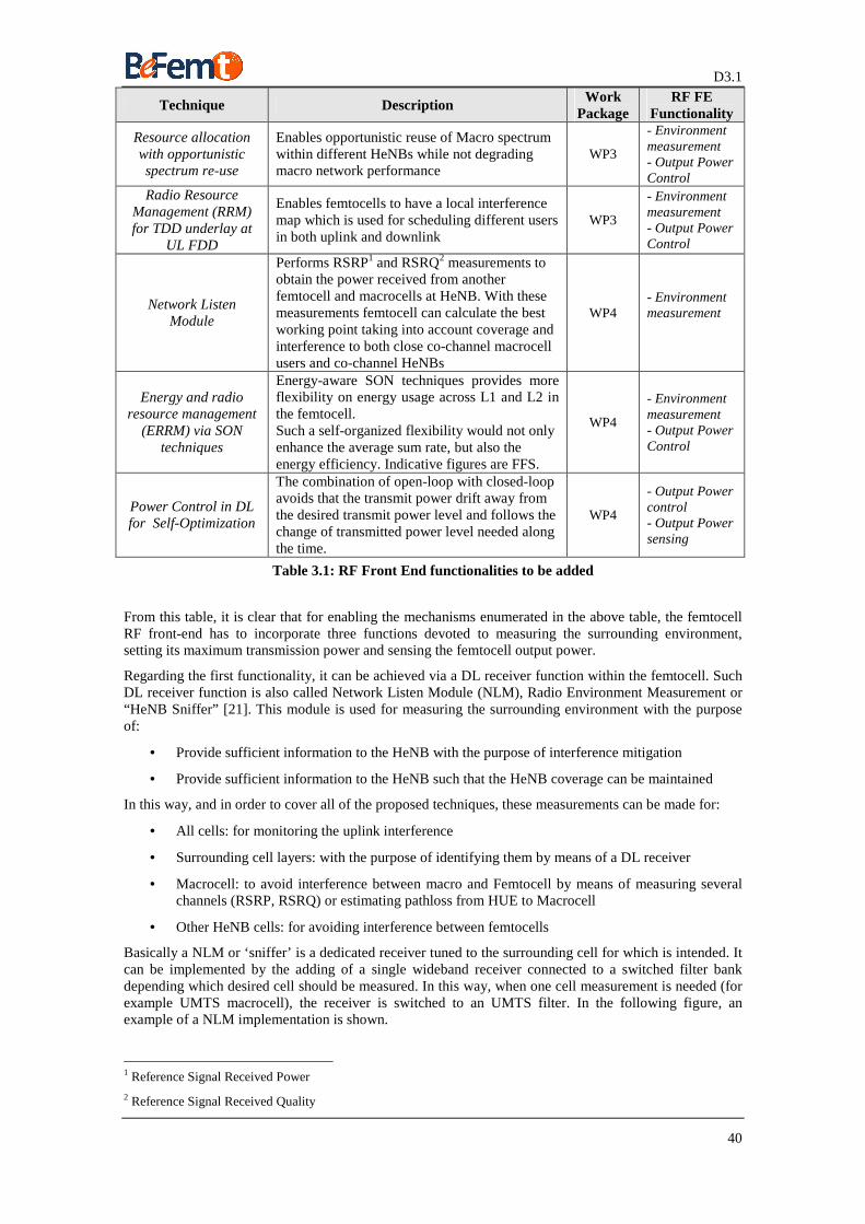
D3.1
40
Technique Description Work
Package RF FE
Functionality
Resource allocation with opportunistic spectrum re-use
Enables opportunistic reuse of Macro spectrum within different HeNBs while not degrading macro network performance
WP3
- Environment measurement - Output Power Control
Radio Resource Management (RRM) for TDD underlay at
UL FDD
Enables femtocells to have a local interference map which is used for scheduling different users in both uplink and downlink
WP3
- Environment measurement - Output Power Control
Network Listen Module
Performs RSRP1 and RSRQ2 measurements to obtain the power received from another femtocell and macrocells at HeNB. With these measurements femtocell can calculate the best working point taking into account coverage and interference to both close co-channel macrocell users and co-channel HeNBs
WP4 - Environment measurement
Energy and radio resource management
(ERRM) via SON techniques
Energy-aware SON techniques provides more flexibility on energy usage across L1 and L2 in the femtocell. Such a self-organized flexibility would not only enhance the average sum rate, but also the energy efficiency. Indicative figures are FFS.
WP4
- Environment measurement - Output Power Control
Power Control in DL for Self-Optimization
The combination of open-loop with closed-loop avoids that the transmit power drift away from the desired transmit power level and follows the change of transmitted power level needed along the time.
WP4
- Output Power control - Output Power sensing
Table 3.1: RF Front End functionalities to be added
From this table, it is clear that for enabling the mechanisms enumerated in the above table, the femtocell RF front-end has to incorporate three functions devoted to measuring the surrounding environment, setting its maximum transmission power and sensing the femtocell output power.
Regarding the first functionality, it can be achieved via a DL receiver function within the femtocell. Such DL receiver function is also called Network Listen Module (NLM), Radio Environment Measurement or “HeNB Sniffer” [21]. This module is used for measuring the surrounding environment with the purpose of:
• Provide sufficient information to the HeNB with the purpose of interference mitigation
• Provide sufficient information to the HeNB such that the HeNB coverage can be maintained
In this way, and in order to cover all of the proposed techniques, these measurements can be made for:
• All cells: for monitoring the uplink interference
• Surrounding cell layers: with the purpose of identifying them by means of a DL receiver
• Macrocell: to avoid interference between macro and Femtocell by means of measuring several channels (RSRP, RSRQ) or estimating pathloss from HUE to Macrocell
• Other HeNB cells: for avoiding interference between femtocells
Basically a NLM or ‘sniffer’ is a dedicated receiver tuned to the surrounding cell for which is intended. It can be implemented by the adding of a single wideband receiver connected to a switched filter bank depending which desired cell should be measured. In this way, when one cell measurement is needed (for example UMTS macrocell), the receiver is switched to an UMTS filter. In the following figure, an example of a NLM implementation is shown.
1 Reference Signal Received Power
2 Reference Signal Received Quality
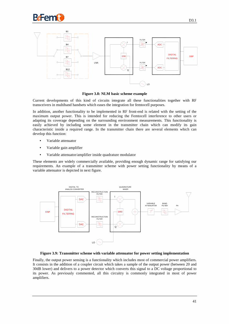
D3.1
41
LO
LNA
I
Q
0/90
FILTER
FILTER
FILTERING
ADC
ADC
DIGITAL DSP
B1
B4
B7
B12
Figure 3.8: NLM basic scheme example
Current developments of this kind of circuits integrate all these functionalities together with RF transceivers in multiband handsets which eases the integration for femtocell purposes.
In addition, another functionality to be implemented in RF front-end is related with the setting of the maximum output power. This is intended for reducing the Femtocell interference to other users or adapting its coverage depending on the surrounding environment measurements. This functionality is easily achieved by including some element in the transmitter chain which can modify its gain characteristic inside a required range. In the transmitter chain there are several elements which can develop this function:
• Variable attenuator
• Variable gain amplifier
• Variable attenuator/amplifier inside quadrature modulator
These elements are widely commercially available, providing enough dynamic range for satisfying our requirements. An example of a transmitter scheme with power setting functionality by means of a variable attenuator is depicted in next figure.
DAC
DAC
DIGITAL
FILTERING
RECONSTRUCTIONFILTER
FILTERRECONSTRUCTION
0/90
LO
QUADRATUREMIXER
DIGITAL TOANALOG CONVERTER
DSP
I
Q
BANDFILTER PAATTENUATOR
VARIABLE
Figure 3.9: Transmitter scheme with variable attenuator for power setting implementation
Finally, the output power sensing is a functionality which includes most of commercial power amplifiers. It consists in the addition of a coupler circuit which takes a sample of the output power (between 20 and 30dB lower) and delivers to a power detector which converts this signal to a DC voltage proportional to its power. As previously commented, all this circuitry is commonly integrated in most of power amplifiers.
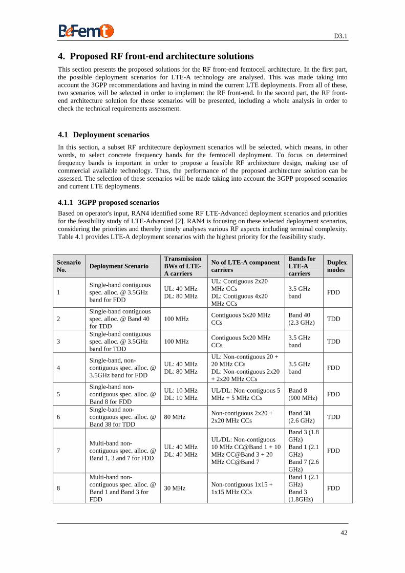
D3.1
42
4. Proposed RF front-end architecture solutions This section presents the proposed solutions for the RF front-end femtocell architecture. In the first part, the possible deployment scenarios for LTE-A technology are analysed. This was made taking into account the 3GPP recommendations and having in mind the current LTE deployments. From all of these, two scenarios will be selected in order to implement the RF front-end. In the second part, the RF front-end architecture solution for these scenarios will be presented, including a whole analysis in order to check the technical requirements assessment.
4.1 Deployment scenarios
In this section, a subset RF architecture deployment scenarios will be selected, which means, in other words, to select concrete frequency bands for the femtocell deployment. To focus on determined frequency bands is important in order to propose a feasible RF architecture design, making use of commercial available technology. Thus, the performance of the proposed architecture solution can be assessed. The selection of these scenarios will be made taking into account the 3GPP proposed scenarios and current LTE deployments.
4.1.1 3GPP proposed scenarios Based on operator's input, RAN4 identified some RF LTE-Advanced deployment scenarios and priorities for the feasibility study of LTE-Advanced [2]. RAN4 is focusing on these selected deployment scenarios, considering the priorities and thereby timely analyses various RF aspects including terminal complexity. Table 4.1 provides LTE-A deployment scenarios with the highest priority for the feasibility study.
Scenario No. Deployment Scenario
Transmission BWs of LTE-A carriers
No of LTE-A component carriers
Bands for LTE-A carriers
Duplex modes
1 Single-band contiguous spec. alloc. @ 3.5GHz band for FDD
UL: 40 MHz DL: 80 MHz
UL: Contiguous 2x20 MHz CCs DL: Contiguous 4x20 MHz CCs
3.5 GHz band
FDD
2 Single-band contiguous spec. alloc. @ Band 40 for TDD
100 MHz Contiguous 5x20 MHz CCs
Band 40 (2.3 GHz)
TDD
3 Single-band contiguous spec. alloc. @ 3.5GHz band for TDD
100 MHz Contiguous 5x20 MHz CCs
3.5 GHz band
TDD
4 Single-band, non-contiguous spec. alloc. @ 3.5GHz band for FDD
UL: 40 MHz DL: 80 MHz
UL: Non-contiguous 20 + 20 MHz CCs DL: Non-contiguous 2x20 + 2x20 MHz CCs
3.5 GHz band
FDD
5 Single-band non-contiguous spec. alloc. @ Band 8 for FDD
UL: 10 MHz DL: 10 MHz
UL/DL: Non-contiguous 5 MHz + 5 MHz CCs
Band 8 (900 MHz)
FDD
6 Single-band non-contiguous spec. alloc. @ Band 38 for TDD
80 MHz Non-contiguous 2x20 + 2x20 MHz CCs
Band 38 (2.6 GHz)
TDD
7 Multi-band non-contiguous spec. alloc. @ Band 1, 3 and 7 for FDD
UL: 40 MHz DL: 40 MHz
UL/DL: Non-contiguous 10 MHz CC@Band 1 + 10 MHz CC@Band 3 + 20 MHz CC@Band 7
Band 3 (1.8 GHz) Band 1 (2.1 GHz) Band 7 (2.6 GHz)
FDD
8
Multi-band non-contiguous spec. alloc. @ Band 1 and Band 3 for FDD
30 MHz Non-contiguous 1x15 + 1x15 MHz CCs
Band 1 (2.1 GHz) Band 3 (1.8GHz)
FDD
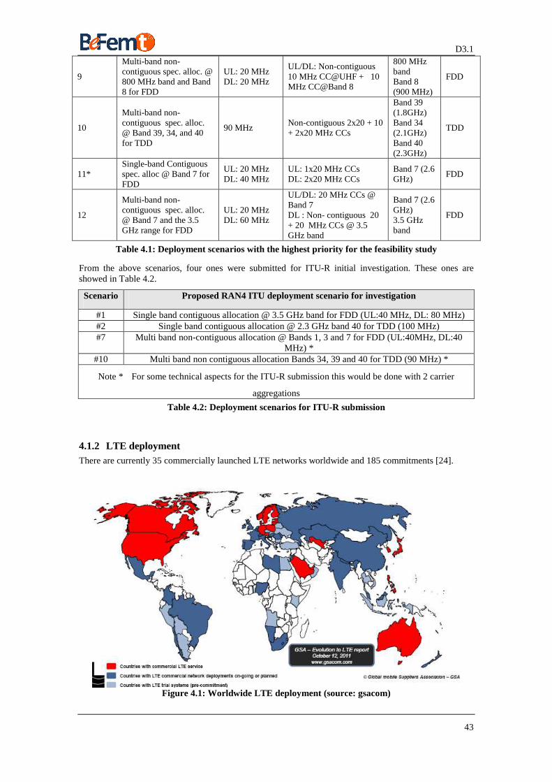
D3.1
43
Table 4.1: Deployment scenarios with the highest priority for the feasibility study
From the above scenarios, four ones were submitted for ITU-R initial investigation. These ones are showed in Table 4.2.
Scenario Proposed RAN4 ITU deployment scenario for investigation
#1 Single band contiguous allocation @ 3.5 GHz band for FDD (UL:40 MHz, DL: 80 MHz) #2 Single band contiguous allocation @ 2.3 GHz band 40 for TDD (100 MHz) #7 Multi band non-contiguous allocation @ Bands 1, 3 and 7 for FDD (UL:40MHz, DL:40
MHz) * #10 Multi band non contiguous allocation Bands 34, 39 and 40 for TDD (90 MHz) *
Note * For some technical aspects for the ITU-R submission this would be done with 2 carrier
aggregations
Table 4.2: Deployment scenarios for ITU-R submission
4.1.2 LTE deployment There are currently 35 commercially launched LTE networks worldwide and 185 commitments [24].
Figure 4.1: Worldwide LTE deployment (source: gsacom)
9
Multi-band non-contiguous spec. alloc. @ 800 MHz band and Band 8 for FDD
UL: 20 MHz DL: 20 MHz
UL/DL: Non-contiguous 10 MHz CC@UHF + 10 MHz CC@Band 8
800 MHz band Band 8 (900 MHz)
FDD
10
Multi-band non-contiguous spec. alloc. @ Band 39, 34, and 40 for TDD
90 MHz Non-contiguous 2x20 + 10 + 2x20 MHz CCs
Band 39 (1.8GHz) Band 34 (2.1GHz) Band 40 (2.3GHz)
TDD
11* Single-band Contiguous spec. alloc @ Band 7 for FDD
UL: 20 MHz DL: 40 MHz
UL: 1x20 MHz CCs DL: 2x20 MHz CCs
Band 7 (2.6 GHz)
FDD
12
Multi-band non-contiguous spec. alloc. @ Band 7 and the 3.5 GHz range for FDD
UL: 20 MHz DL: 60 MHz
UL/DL: 20 MHz CCs @ Band 7 DL : Non- contiguous 20 + 20 MHz CCs @ 3.5 GHz band
Band 7 (2.6 GHz) 3.5 GHz band
FDD
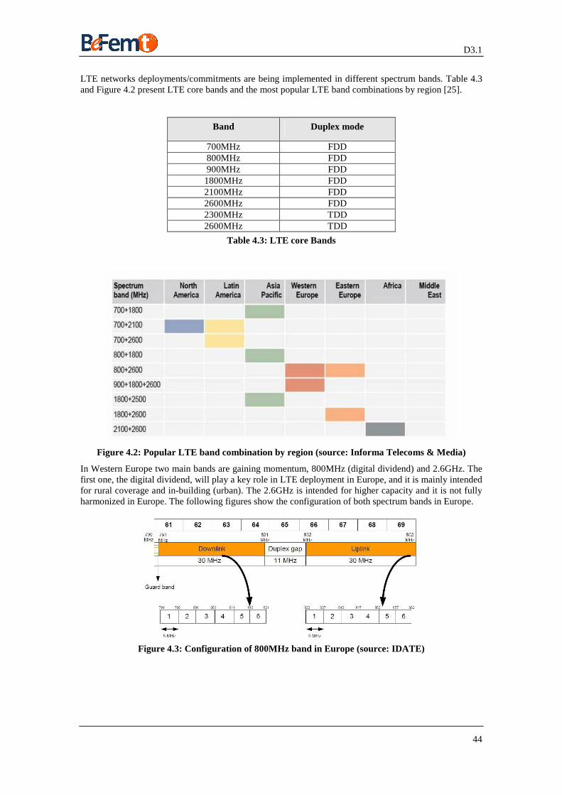
D3.1
44
LTE networks deployments/commitments are being implemented in different spectrum bands. Table 4.3 and Figure 4.2 present LTE core bands and the most popular LTE band combinations by region [25].
Band Duplex mode
700MHz FDD 800MHz FDD 900MHz FDD 1800MHz FDD 2100MHz FDD 2600MHz FDD 2300MHz TDD 2600MHz TDD
Table 4.3: LTE core Bands
Figure 4.2: Popular LTE band combination by region (source: Informa Telecoms & Media)
In Western Europe two main bands are gaining momentum, 800MHz (digital dividend) and 2.6GHz. The first one, the digital dividend, will play a key role in LTE deployment in Europe, and it is mainly intended for rural coverage and in-building (urban). The 2.6GHz is intended for higher capacity and it is not fully harmonized in Europe. The following figures show the configuration of both spectrum bands in Europe.
Figure 4.3: Configuration of 800MHz band in Europe (source: IDATE)
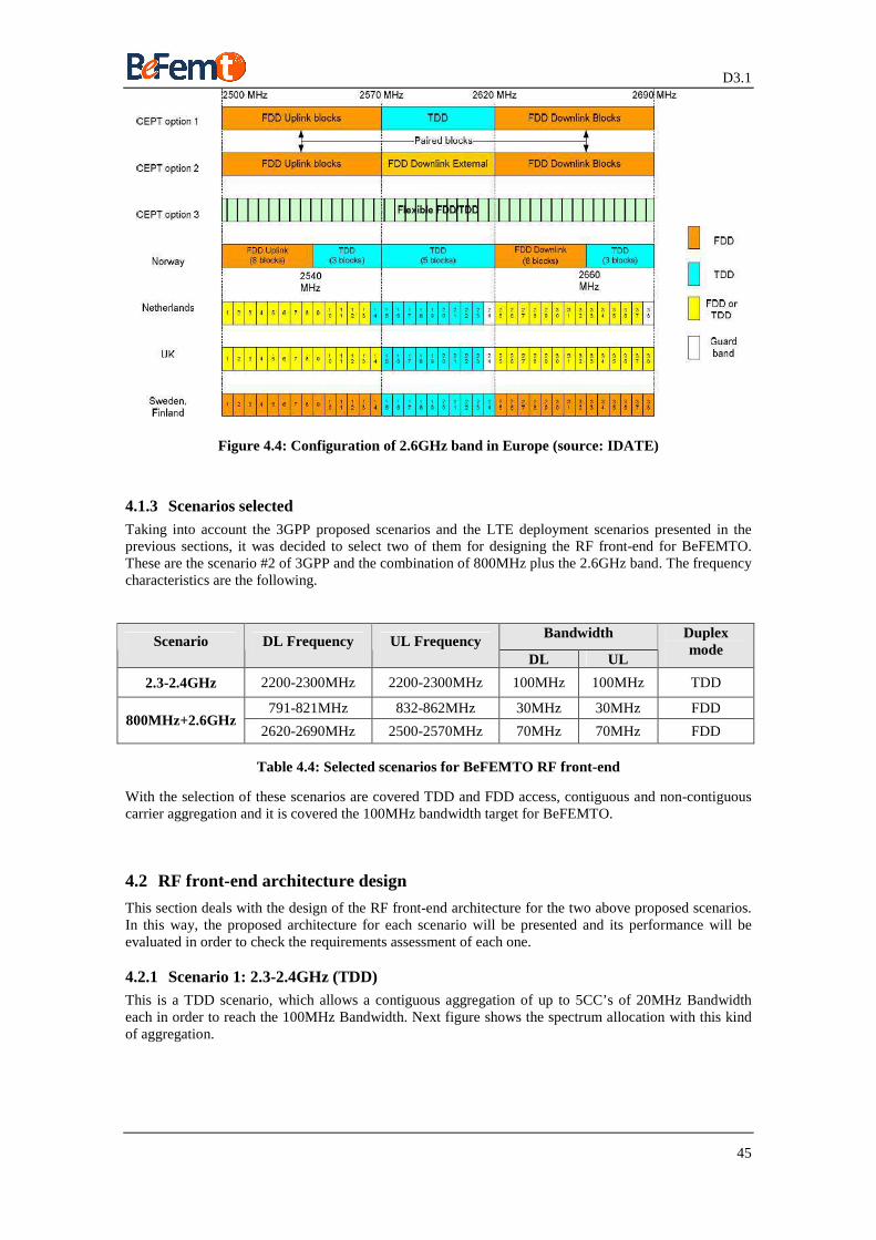
D3.1
45
Figure 4.4: Configuration of 2.6GHz band in Europe (source: IDATE)
4.1.3 Scenarios selected Taking into account the 3GPP proposed scenarios and the LTE deployment scenarios presented in the previous sections, it was decided to select two of them for designing the RF front-end for BeFEMTO. These are the scenario #2 of 3GPP and the combination of 800MHz plus the 2.6GHz band. The frequency characteristics are the following.
Bandwidth Scenario DL Frequency UL Frequency
DL UL
Duplex mode
2.3-2.4GHz 2200-2300MHz 2200-2300MHz 100MHz 100MHz TDD
791-821MHz 832-862MHz 30MHz 30MHz FDD 800MHz+2.6GHz
2620-2690MHz 2500-2570MHz 70MHz 70MHz FDD
Table 4.4: Selected scenarios for BeFEMTO RF front-end
With the selection of these scenarios are covered TDD and FDD access, contiguous and non-contiguous carrier aggregation and it is covered the 100MHz bandwidth target for BeFEMTO.
4.2 RF front-end architecture design
This section deals with the design of the RF front-end architecture for the two above proposed scenarios. In this way, the proposed architecture for each scenario will be presented and its performance will be evaluated in order to check the requirements assessment of each one.
4.2.1 Scenario 1: 2.3-2.4GHz (TDD) This is a TDD scenario, which allows a contiguous aggregation of up to 5CC’s of 20MHz Bandwidth each in order to reach the 100MHz Bandwidth. Next figure shows the spectrum allocation with this kind of aggregation.
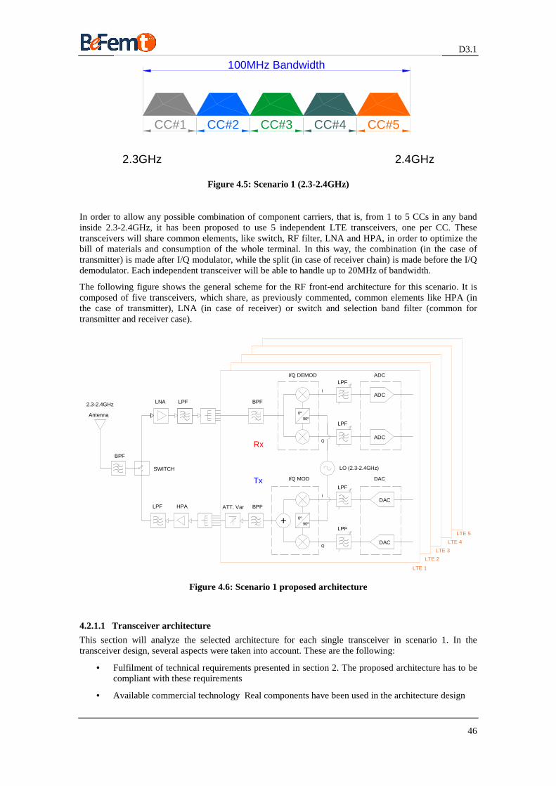
D3.1
46
2.4GHz
100MHz Bandwidth
CC#5
2.3GHz
CC#1 CC#3CC#2 CC#4
Figure 4.5: Scenario 1 (2.3-2.4GHz)
In order to allow any possible combination of component carriers, that is, from 1 to 5 CCs in any band inside 2.3-2.4GHz, it has been proposed to use 5 independent LTE transceivers, one per CC. These transceivers will share common elements, like switch, RF filter, LNA and HPA, in order to optimize the bill of materials and consumption of the whole terminal. In this way, the combination (in the case of transmitter) is made after I/Q modulator, while the split (in case of receiver chain) is made before the I/Q demodulator. Each independent transceiver will be able to handle up to 20MHz of bandwidth.
The following figure shows the general scheme for the RF front-end architecture for this scenario. It is composed of five transceivers, which share, as previously commented, common elements like HPA (in the case of transmitter), LNA (in case of receiver) or switch and selection band filter (common for transmitter and receiver case).
LNA
HPA
0º90º
LPF
LPF
ADC
ADC
DAC
0º90º
LPF
LPF
DAC
I
Q
I
Q
+
LO (2.3-2.4GHz)
Antenna
SWITCH
BPF
LPF
LPF
ATT. Var
I/Q DEMOD
I/Q MOD
ADC
DAC
LTE 1
LTE 2
LTE 3
LTE 4
LTE 5
Rx
Tx
2.3-2.4GHz
BPF
BPF
Figure 4.6: Scenario 1 proposed architecture
4.2.1.1 Transceiver architecture
This section will analyze the selected architecture for each single transceiver in scenario 1. In the transceiver design, several aspects were taken into account. These are the following:
• Fulfilment of technical requirements presented in section 2. The proposed architecture has to be compliant with these requirements
• Available commercial technology Real components have been used in the architecture design
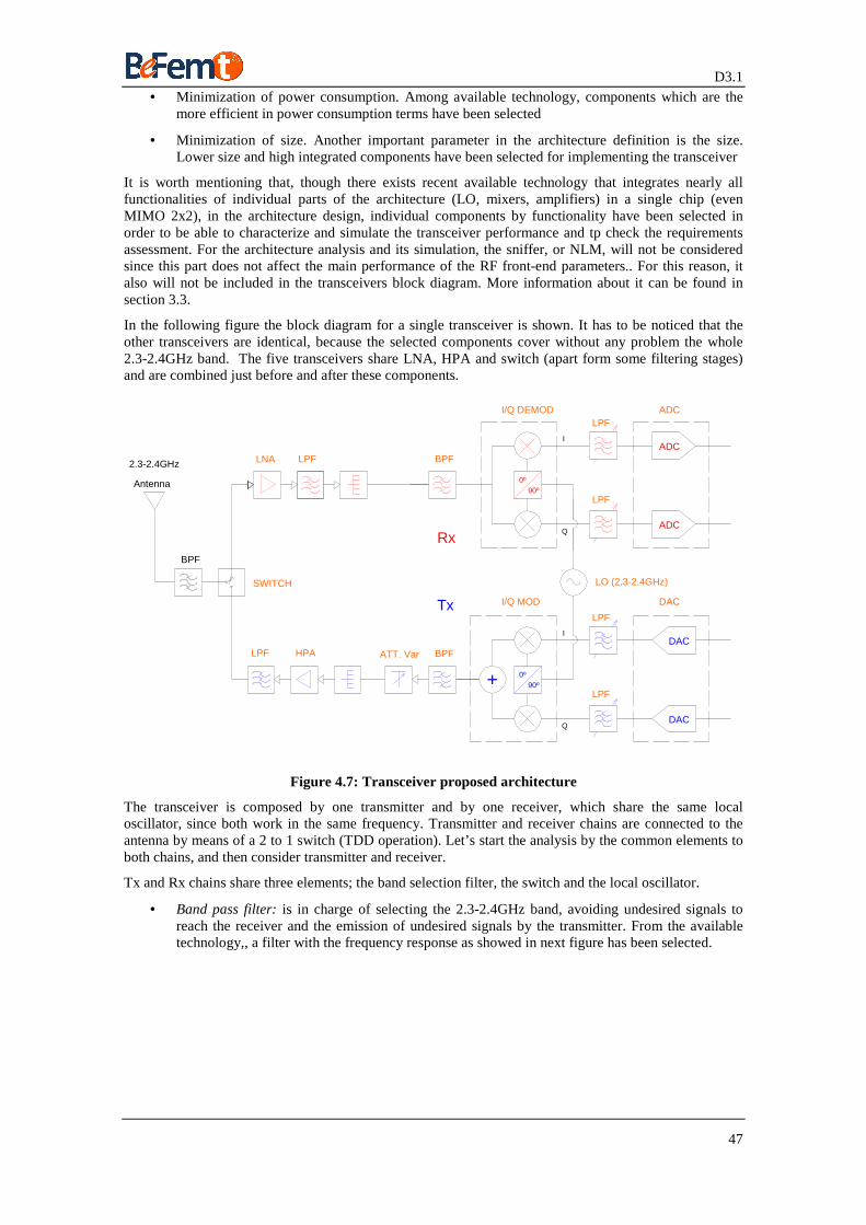
D3.1
47
• Minimization of power consumption. Among available technology, components which are the more efficient in power consumption terms have been selected
• Minimization of size. Another important parameter in the architecture definition is the size. Lower size and high integrated components have been selected for implementing the transceiver
It is worth mentioning that, though there exists recent available technology that integrates nearly all functionalities of individual parts of the architecture (LO, mixers, amplifiers) in a single chip (even MIMO 2x2), in the architecture design, individual components by functionality have been selected in order to be able to characterize and simulate the transceiver performance and tp check the requirements assessment. For the architecture analysis and its simulation, the sniffer, or NLM, will not be considered since this part does not affect the main performance of the RF front-end parameters.. For this reason, it also will not be included in the transceivers block diagram. More information about it can be found in section 3.3.
In the following figure the block diagram for a single transceiver is shown. It has to be noticed that the other transceivers are identical, because the selected components cover without any problem the whole 2.3-2.4GHz band. The five transceivers share LNA, HPA and switch (apart form some filtering stages) and are combined just before and after these components.
I/Q MOD
I/Q DEMOD
+
DAC
Q
90º0º
LPF
I
LPF
DAC
DAC
LO (2.3-2.4GHz)
Q
90º0º
LPF
ADC
I
LPFADC
ADC
Antenna
2.3-2.4GHz
LPF
SWITCH
BPF
HPA
LNA LPF
ATT. Var BPF
Tx
Rx
BPF
Figure 4.7: Transceiver proposed architecture
The transceiver is composed by one transmitter and by one receiver, which share the same local oscillator, since both work in the same frequency. Transmitter and receiver chains are connected to the antenna by means of a 2 to 1 switch (TDD operation). Let’s start the analysis by the common elements to both chains, and then consider transmitter and receiver.
Tx and Rx chains share three elements; the band selection filter, the switch and the local oscillator.
• Band pass filter: is in charge of selecting the 2.3-2.4GHz band, avoiding undesired signals to reach the receiver and the emission of undesired signals by the transmitter. From the available technology,, a filter with the frequency response as showed in next figure has been selected.
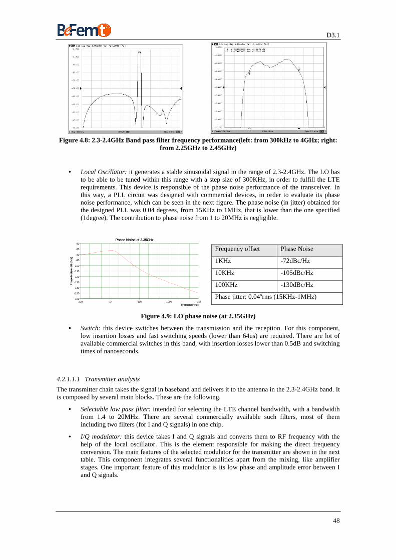
D3.1
48
Figure 4.8: 2.3-2.4GHz Band pass filter frequency performance(left: from 300kHz to 4GHz; right:
from 2.25GHz to 2.45GHz)
• Local Oscillator: it generates a stable sinusoidal signal in the range of 2.3-2.4GHz. The LO has
to be able to be tuned within this range with a step size of 300KHz, in order to fulfill the LTE requirements. This device is responsible of the phase noise performance of the transceiver. In this way, a PLL circuit was designed with commercial devices, in order to evaluate its phase noise performance, which can be seen in the next figure. The phase noise (in jitter) obtained for the designed PLL was 0.04 degrees, from 15KHz to 1MHz, that is lower than the one specified (1degree). The contribution to phase noise from 1 to 20MHz is negligible.
100 1k 10k 100k 1MFrequency (Hz)
-160
-150
-140
-130
-120
-110
-100
-90
-80
-70
-60
Ph
ase
No
ise
(dB
c/H
z)
Phase Noise at 2.35GHz
Frequency offset Phase Noise
1KHz -72dBc/Hz
10KHz -105dBc/Hz
100KHz -130dBc/Hz
Phase jitter: 0.04ºrms (15KHz-1MHz)
Figure 4.9: LO phase noise (at 2.35GHz)
• Switch: this device switches between the transmission and the reception. For this component, low insertion losses and fast switching speeds (lower than 64us) are required. There are lot of available commercial switches in this band, with insertion losses lower than 0.5dB and switching times of nanoseconds.
4.2.1.1.1 Transmitter analysis
The transmitter chain takes the signal in baseband and delivers it to the antenna in the 2.3-2.4GHz band. It is composed by several main blocks. These are the following.
• Selectable low pass filter: intended for selecting the LTE channel bandwidth, with a bandwidth from 1.4 to 20MHz. There are several commercially available such filters, most of them including two filters (for I and Q signals) in one chip.
• I/Q modulator: this device takes I and Q signals and converts them to RF frequency with the help of the local oscillator. This is the element responsible for making the direct frequency conversion. The main features of the selected modulator for the transmitter are shown in the next table. This component integrates several functionalities apart from the mixing, like amplifier stages. One important feature of this modulator is its low phase and amplitude error between I and Q signals.
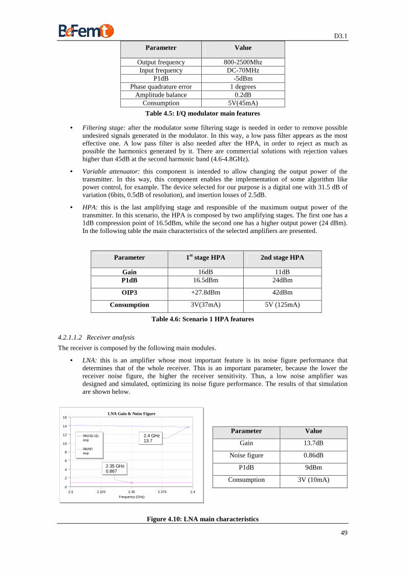
D3.1
49
Parameter Value
Output frequency 800-2500Mhz Input frequency DC-70MHz
P1dB -5dBm Phase quadrature error 1 degrees
Amplitude balance 0.2dB Consumption 5V(45mA)
Table 4.5: I/Q modulator main features
• Filtering stage: after the modulator some filtering stage is needed in order to remove possible undesired signals generated in the modulator. In this way, a low pass filter appears as the most effective one. A low pass filter is also needed after the HPA, in order to reject as much as possible the harmonics generated by it. There are commercial solutions with rejection values higher than 45dB at the second harmonic band (4.6-4.8GHz).
• Variable attenuator: this component is intended to allow changing the output power of the transmitter. In this way, this component enables the implementation of some algorithm like power control, for example. The device selected for our purpose is a digital one with 31.5 dB of variation (6bits, 0.5dB of resolution), and insertion losses of 2.5dB.
• HPA: this is the last amplifying stage and responsible of the maximum output power of the transmitter. In this scenario, the HPA is composed by two amplifying stages. The first one has a 1dB compression point of 16.5dBm, while the second one has a higher output power (24 dBm). In the following table the main characteristics of the selected amplifiers are presented.
Parameter 1st stage HPA 2nd stage HPA
Gain 16dB 11dB P1dB 16.5dBm 24dBm
OIP3 +27.8dBm 42dBm
Consumption 3V(37mA) 5V (125mA)
Table 4.6: Scenario 1 HPA features
4.2.1.1.2 Receiver analysis
The receiver is composed by the following main modules.
• LNA: this is an amplifier whose most important feature is its noise figure performance that determines that of the whole receiver. This is an important parameter, because the lower the receiver noise figure, the higher the receiver sensitivity. Thus, a low noise amplifier was designed and simulated, optimizing its noise figure performance. The results of that simulation are shown below.
2.3 2.325 2.35 2.375 2.4Frequency (GHz)
LNA Gain & Noise Figure
0
2
4
6
8
10
12
14
16
2.35 GHz 0.867
2.4 GHz 13.7
DB(|S[2,1]|)Amp
DB(NF)Amp
Parameter Value
Gain 13.7dB
Noise figure 0.86dB
P1dB 9dBm
Consumption 3V (10mA)
Figure 4.10: LNA main characteristics

D3.1
50
• Filtering stages: a couple of filtering stages are foreseen, in order to avoid the input of undesired signals to the demodulator, first, and second to avoid that any mixing product generated in the demodulator reach the antenna port. In this way, a low pass filter and a band pass one are foreseen. These are the same than the ones used in the transmitter part, with rejection values higher than 45dB to the second signal harmonic.
• I/Q demodulator: fulfills the dual functions of the modulator, viz., it takes the signal in RF and delivers it in baseband with the help of the local oscillator signal. The main features of the I/Q demodulator selected for this purpose are shown below. This component incorporates also several added functionalities like amplifier stages (in RF and Baseband) including Automatic Level Control. It has also a low phase and amplitude imbalance between I and Q branches.
Parameter Value
Input frequency 800 to 2700MHz Output frequency DC-65MHz
Quadrature phase error 1 degree Amplitude balance 0.3dB
Consumption 5V (64mA)
Table 4.7: I/Q demodulator main features
• Selectable low pass filter: it is intended for selecting the appropriate LTE channel (with bandwidths from 1.4 to 20MHz). This device is identical to the one used in the transmitter case.
4.2.1.1.3 Transceiver power consumption
One important feature of the transceiver is its power consumption. All of the components which form part of the transceivers have been selected following low consumption criteria, in order to minimize the overall consumption budget of the transceiver. The following table summarizes the power consumption budget of the RF front-end part, for one and five transceivers.
Module Consumption Number of
modules per 5 transceivers
Consumption of 1 Transceiver
(mW)
Consumption of 5 Transceivers
(mW)
SWITCH (Rx/Tx) 0 1 0 0 LNA (Rx) 3V (10mA) 1 30 30 HPA (Tx) 5V(125mA)
3V(37mA) 1 1
736 736
VARIABLE ATTENUATOR(Tx)
5V (1mA) 5 5 25
I/Q MODULATOR (Tx)
5V (45mA) 5 225 1125
VCO (Tx/Rx) 5V (40mA) 5 200 1000 PLL Frequency
Synthesizer (Tx/Rx) 3.3V (3mA) 5 10 50
PROGRAMMABLE LPF (Tx)
3.3V (59mA) 5 195 975
I/Q DEMODULATOR(Rx)
5V (64mA) 5 320 1600
PROGRAMMABLE LPF (Rx)
3.3V (59mA) 5 195 975
Total consumption 1916 6516
Table 4.8: Scenario 1 estimated RF front-end power consumption
For this architecture, the total estimated power consumption is around 6.5W when the 5 transceivers are used, covering the 100MHz. It has to be noticed that for this scenario, it is possible to reduce the overall consumption by applying energy saving techniques, eg., by switching off the transmitter when the transceiver is only receiving.
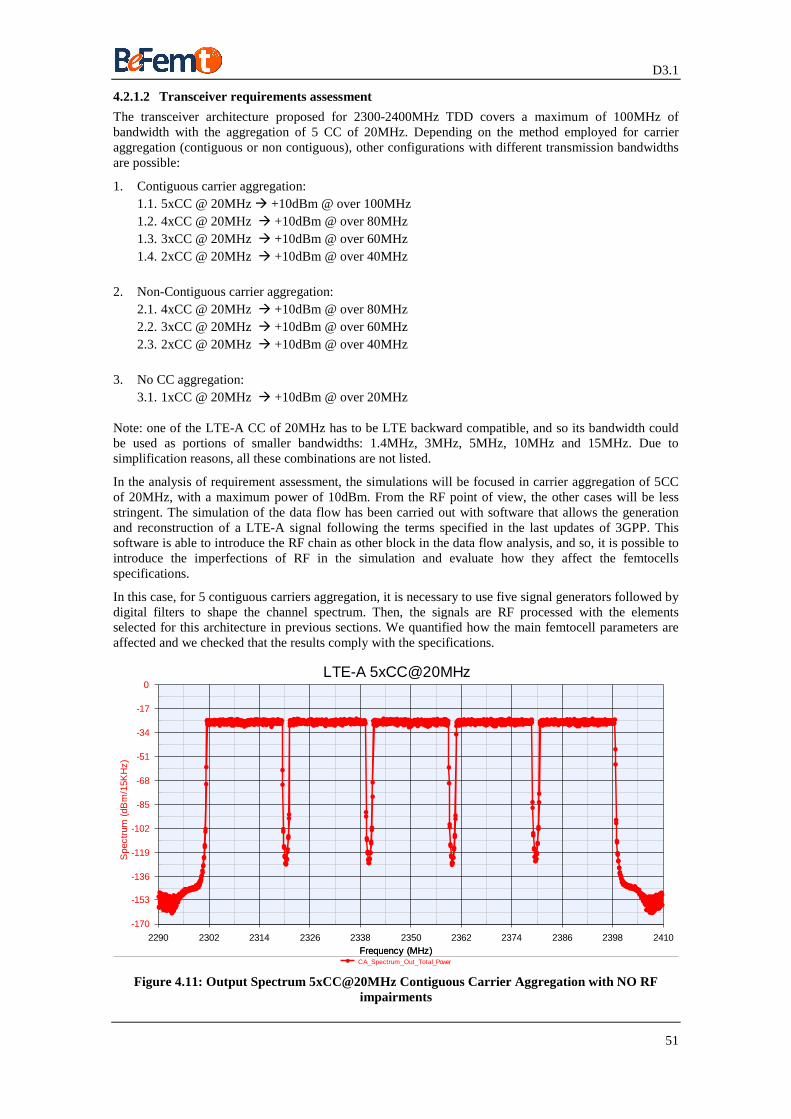
D3.1
51
4.2.1.2 Transceiver requirements assessment
The transceiver architecture proposed for 2300-2400MHz TDD covers a maximum of 100MHz of bandwidth with the aggregation of 5 CC of 20MHz. Depending on the method employed for carrier aggregation (contiguous or non contiguous), other configurations with different transmission bandwidths are possible:
1. Contiguous carrier aggregation: 1.1. 5xCC @ 20MHz � +10dBm @ over 100MHz 1.2. 4xCC @ 20MHz � +10dBm @ over 80MHz 1.3. 3xCC @ 20MHz � +10dBm @ over 60MHz 1.4. 2xCC @ 20MHz � +10dBm @ over 40MHz
2. Non-Contiguous carrier aggregation:
2.1. 4xCC @ 20MHz � +10dBm @ over 80MHz 2.2. 3xCC @ 20MHz � +10dBm @ over 60MHz 2.3. 2xCC @ 20MHz � +10dBm @ over 40MHz
3. No CC aggregation:
3.1. 1xCC @ 20MHz � +10dBm @ over 20MHz
Note: one of the LTE-A CC of 20MHz has to be LTE backward compatible, and so its bandwidth could be used as portions of smaller bandwidths: 1.4MHz, 3MHz, 5MHz, 10MHz and 15MHz. Due to simplification reasons, all these combinations are not listed.
In the analysis of requirement assessment, the simulations will be focused in carrier aggregation of 5CC of 20MHz, with a maximum power of 10dBm. From the RF point of view, the other cases will be less stringent. The simulation of the data flow has been carried out with software that allows the generation and reconstruction of a LTE-A signal following the terms specified in the last updates of 3GPP. This software is able to introduce the RF chain as other block in the data flow analysis, and so, it is possible to introduce the imperfections of RF in the simulation and evaluate how they affect the femtocells specifications.
In this case, for 5 contiguous carriers aggregation, it is necessary to use five signal generators followed by digital filters to shape the channel spectrum. Then, the signals are RF processed with the elements selected for this architecture in previous sections. We quantified how the main femtocell parameters are affected and we checked that the results comply with the specifications.
Frequency (MHz)
Spe
ctru
m (
dBm
/15K
Hz)
-170
-153
-136
-119
-102
-85
-68
-51
-34
-17
0
Frequency (MHz)2290 2302 2314 2326 2338 2350 2362 2374 2386 2398 2410
LTE-A 5xCC@20MHz
CA_Spectrum_Out_Total_Power
Figure 4.11: Output Spectrum 5xCC@20MHz Contiguous Carrier Aggregation with NO RF impairments
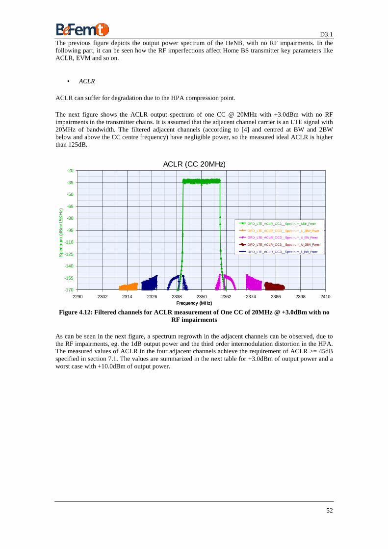
D3.1
52
The previous figure depicts the output power spectrum of the HeNB, with no RF impairments. In the following part, it can be seen how the RF imperfections affect Home BS transmitter key parameters like ACLR, EVM and so on.
• ACLR
ACLR can suffer for degradation due to the HPA compression point.
The next figure shows the ACLR output spectrum of one CC @ 20MHz with +3.0dBm with no RF impairments in the transmitter chains. It is assumed that the adjacent channel carrier is an LTE signal with 20MHz of bandwidth. The filtered adjacent channels (according to [4] and centred at BW and 2BW below and above the CC centre frequency) have negligible power, so the measured ideal ACLR is higher than 125dB.
Frequency (MHz)
Spe
ctru
m (
dBm
/15K
Hz)
-170
-155
-140
-125
-110
-95
-80
-65
-50
-35
-20
Frequency (MHz)2290 2302 2314 2326 2338 2350 2362 2374 2386 2398 2410
ACLR (CC 20MHz)
DPD_LTE_ACLR_CC3__Spectrum_Main_Power
DPD_LTE_ACLR_CC3__Spectrum_L_2BW_Power
DPD_LTE_ACLR_CC3__Spectrum_U_BW_Power
DPD_LTE_ACLR_CC3__Spectrum_U_2BW_Power
DPD_LTE_ACLR_CC3__Spectrum_L_BW_Power
Figure 4.12: Filtered channels for ACLR measurement of One CC of 20MHz @ +3.0dBm with no RF impairments
As can be seen in the next figure, a spectrum regrowth in the adjacent channels can be observed, due to the RF impairments, eg. the 1dB output power and the third order intermodulation distortion in the HPA. The measured values of ACLR in the four adjacent channels achieve the requirement of ACLR >= 45dB specified in section 7.1. The values are summarized in the next table for +3.0dBm of output power and a worst case with +10.0dBm of output power.
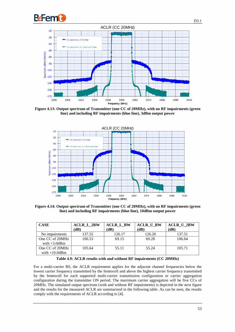
D3.1
53
Frequency (MHz)
Spe
ctru
m (
dBm
/15K
Hz)
-170
-155
-140
-125
-110
-95
-80
-65
-50
-35
-20
Frequency (MHz)2290 2302 2314 2326 2338 2350 2362 2374 2386 2398 2410
ACLR (CC 20MHz)
CA_Spectrum1_CC3_Power
CA_Spectrum1_CC_Bef ore_RF_Power
Figure 4.13: Output spectrum of Transmitter (one CC of 20MHz), with no RF impairments (green
line) and including RF impairments (blue line), 3dBm output power
Frequency (MHz)
Spe
ctru
m (
dBm
/15K
Hz)
-170
-155
-140
-125
-110
-95
-80
-65
-50
-35
-20
Frequency (MHz)2290 2302 2314 2326 2338 2350 2362 2374 2386 2398 2410
ACLR (CC 20MHz)
CA_Spectrum1_CC3_Power
CA_Spectrum1_CC_Bef ore_RF_Power
Figure 4.14: Output spectrum of Transmitter (one CC of 20MHz), with no RF impairments (green line) and including RF impairments (blue line), 10dBm output power
CASE ACLR_L_2BW (dB)
ACLR_L_BW (dB)
ACLR_U_BW (dB)
ACLR_U_2BW (dB)
No impairments 137.55 126.17 126.20 137.51 One CC of 20MHz
with +3.0dBm 106.53 69.15 69.28 106.64
One CC of 20MHz with +10.0dBm
105.64 55.11 55.24 105.71
Table 4.9: ACLR results with and without RF impairments (CC 20MHz)
For a multi-carrier BS, the ACLR requirement applies for the adjacent channel frequencies below the lowest carrier frequency transmitted by the femtocell and above the highest carrier frequency transmitted by the femtocell for each supported multi-carrier transmission configuration or carrier aggregation configuration during the transmitter ON period. The maximum carrier aggregation will be five CCs of 20MHz. The simulated output spectrum (with and without RF impairments) is depicted in the next figure and the results for the measured ACLR are summarized in the following table. As can be seen, the results comply with the requirements of ACLR according to [4].
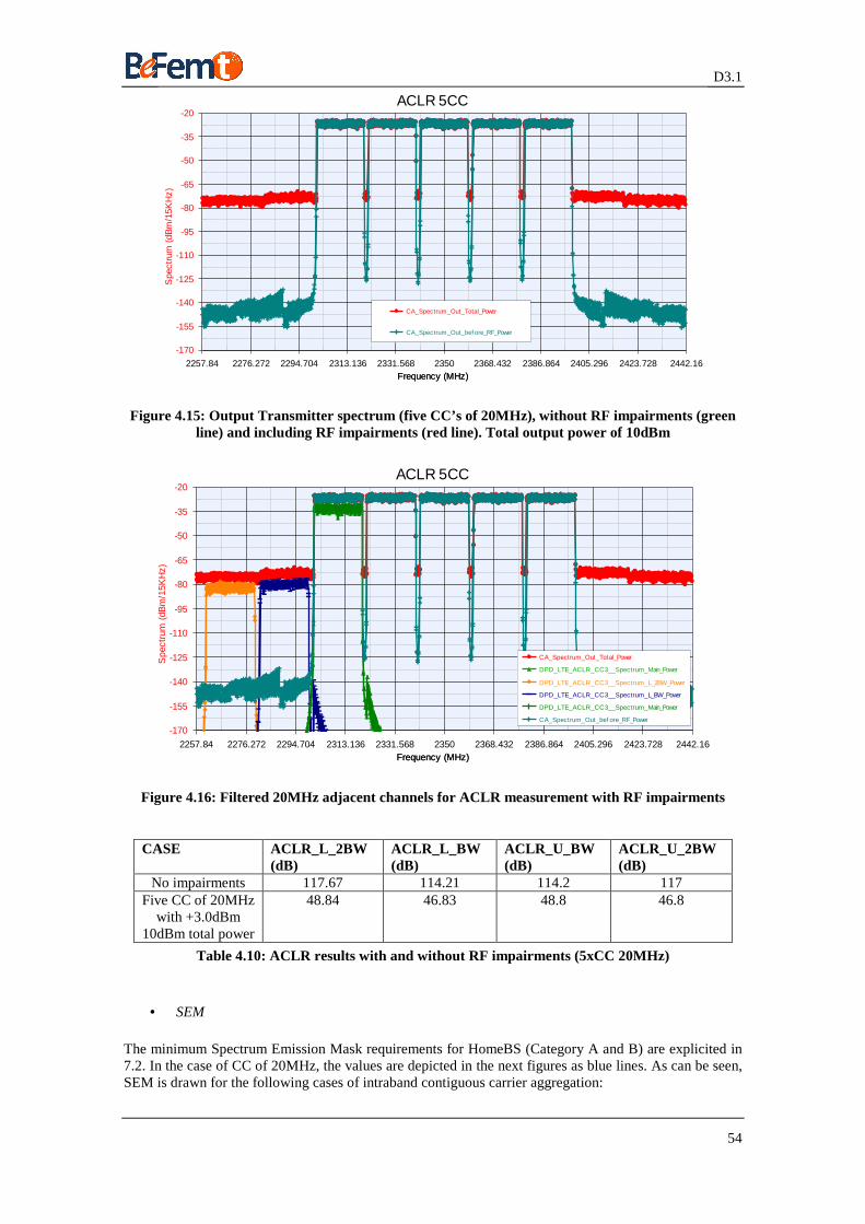
D3.1
54
Frequency (MHz)
Spe
ctru
m (
dBm
/15K
Hz)
-170
-155
-140
-125
-110
-95
-80
-65
-50
-35
-20
Frequency (MHz)2257.84 2276.272 2294.704 2313.136 2331.568 2350 2368.432 2386.864 2405.296 2423.728 2442.16
ACLR 5CC
CA_Spectrum_Out_Total_Power
CA_Spectrum_Out_bef ore_RF_Power
Figure 4.15: Output Transmitter spectrum (five CC’s of 20MHz), without RF impairments (green line) and including RF impairments (red line). Total output power of 10dBm
Frequency (MHz)
Spe
ctru
m (
dBm
/15K
Hz)
-170
-155
-140
-125
-110
-95
-80
-65
-50
-35
-20
Frequency (MHz)2257.84 2276.272 2294.704 2313.136 2331.568 2350 2368.432 2386.864 2405.296 2423.728 2442.16
ACLR 5CC
CA_Spectrum_Out_Total_Power
DPD_LTE_ACLR_CC3__Spectrum_Main_Power
DPD_LTE_ACLR_CC3__Spectrum_L_2BW_Power
DPD_LTE_ACLR_CC3__Spectrum_L_BW_Power
DPD_LTE_ACLR_CC3__Spectrum_Main_Power
CA_Spectrum_Out_bef ore_RF_Power
Figure 4.16: Filtered 20MHz adjacent channels for ACLR measurement with RF impairments
CASE ACLR_L_2BW (dB)
ACLR_L_BW (dB)
ACLR_U_BW (dB)
ACLR_U_2BW (dB)
No impairments 117.67 114.21 114.2 117 Five CC of 20MHz
with +3.0dBm 10dBm total power
48.84 46.83 48.8 46.8
Table 4.10: ACLR results with and without RF impairments (5xCC 20MHz)
• SEM
The minimum Spectrum Emission Mask requirements for HomeBS (Category A and B) are explicited in 7.2. In the case of CC of 20MHz, the values are depicted in the next figures as blue lines. As can be seen, SEM is drawn for the following cases of intraband contiguous carrier aggregation:
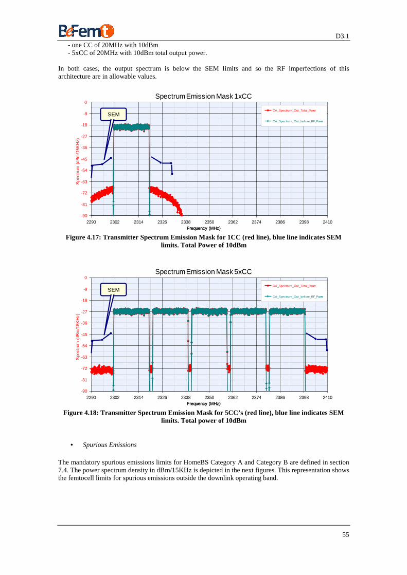
D3.1
55
- one CC of 20MHz with 10dBm - 5xCC of 20MHz with 10dBm total output power.
In both cases, the output spectrum is below the SEM limits and so the RF imperfections of this architecture are in allowable values.
Frequency (MHz)
Spe
ctru
m (
dBm
/15K
Hz)
-90
-81
-72
-63
-54
-45
-36
-27
-18
-9
0
Frequency (MHz)2290 2302 2314 2326 2338 2350 2362 2374 2386 2398 2410
Spectrum Emission Mask 1xCC
CA_Spectrum_Out_Total_Power
CA_Spectrum_Out_bef ore_RF_Power
SEM
Figure 4.17: Transmitter Spectrum Emission Mask for 1CC (red line), blue line indicates SEM
limits. Total Power of 10dBm
Frequency (MHz)
Spe
ctru
m (
dBm
/15K
Hz)
-90
-81
-72
-63
-54
-45
-36
-27
-18
-9
0
Frequency (MHz)2290 2302 2314 2326 2338 2350 2362 2374 2386 2398 2410
Spectrum Emission Mask 5xCC
CA_Spectrum_Out_Total_Power
CA_Spectrum_Out_bef ore_RF_Power
SEM
Figure 4.18: Transmitter Spectrum Emission Mask for 5CC’s (red line), blue line indicates SEM
limits. Total power of 10dBm
• Spurious Emissions
The mandatory spurious emissions limits for HomeBS Category A and Category B are defined in section 7.4. The power spectrum density in dBm/15KHz is depicted in the next figures. This representation shows the femtocell limits for spurious emissions outside the downlink operating band.
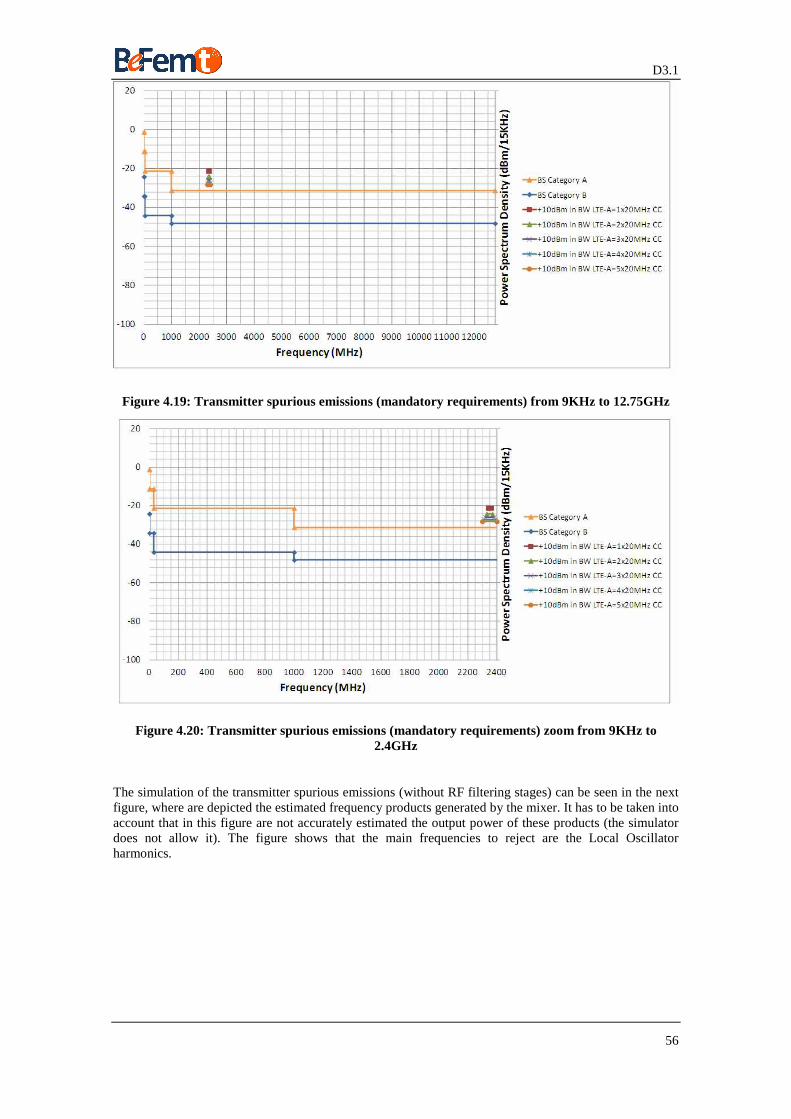
D3.1
56
Figure 4.19: Transmitter spurious emissions (mandatory requirements) from 9KHz to 12.75GHz
Figure 4.20: Transmitter spurious emissions (mandatory requirements) zoom from 9KHz to 2.4GHz
The simulation of the transmitter spurious emissions (without RF filtering stages) can be seen in the next figure, where are depicted the estimated frequency products generated by the mixer. It has to be taken into account that in this figure are not accurately estimated the output power of these products (the simulator does not allow it). The figure shows that the main frequencies to reject are the Local Oscillator harmonics.
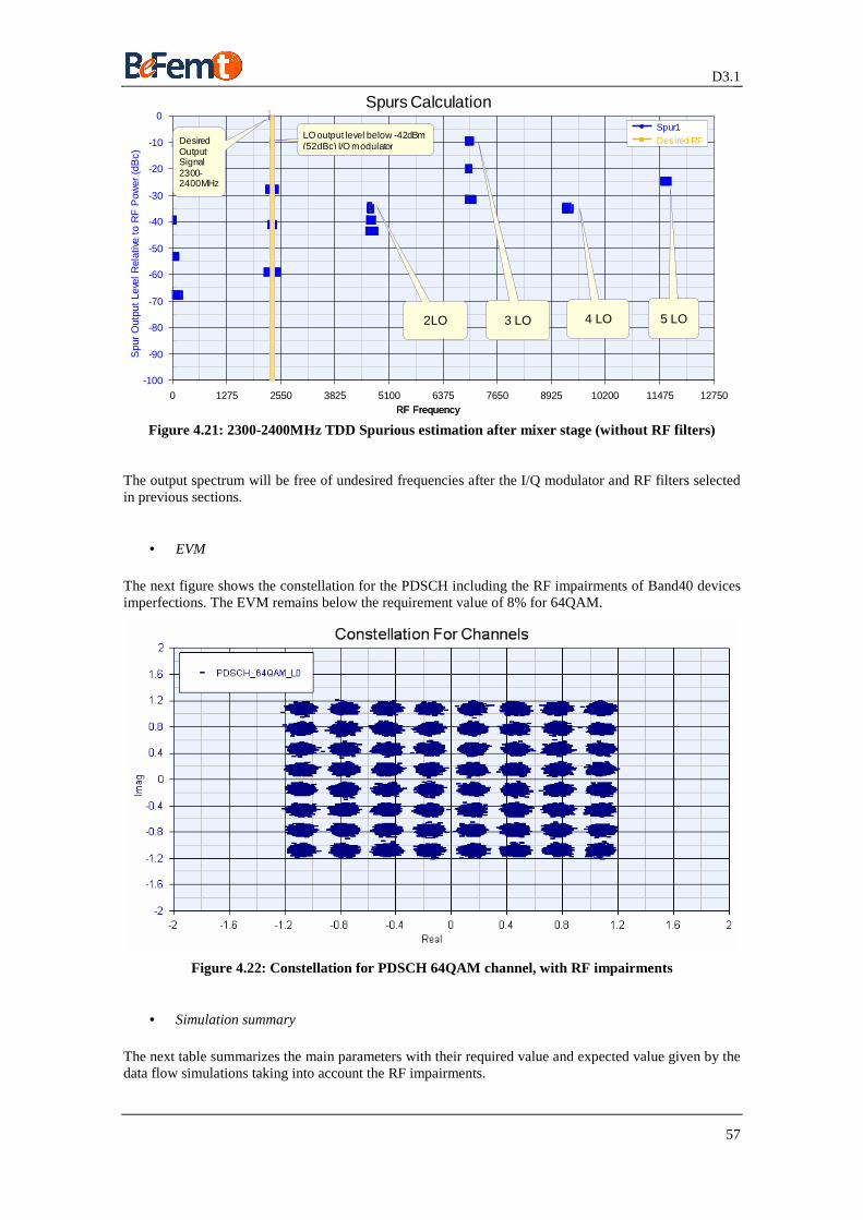
D3.1
57
RF Frequency
Spu
r O
utpu
t Le
vel R
elat
ive
to R
F P
ower
(dB
c)
-100
-90
-80
-70
-60
-50
-40
-30
-20
-10
0
RF Frequency0 1275 2550 3825 5100 6375 7650 8925 10200 11475 12750
Spurs CalculationSpur1Desired RF
LO output level below -42dBm (52dBc) I/Q modulator
Desired Output Signal 2300-2400MHz
2LO 3 LO 4 LO 5 LO
Figure 4.21: 2300-2400MHz TDD Spurious estimation after mixer stage (without RF filters)
The output spectrum will be free of undesired frequencies after the I/Q modulator and RF filters selected in previous sections.
• EVM
The next figure shows the constellation for the PDSCH including the RF impairments of Band40 devices imperfections. The EVM remains below the requirement value of 8% for 64QAM.
Figure 4.22: Constellation for PDSCH 64QAM channel, with RF impairments
• Simulation summary
The next table summarizes the main parameters with their required value and expected value given by the data flow simulations taking into account the RF impairments.
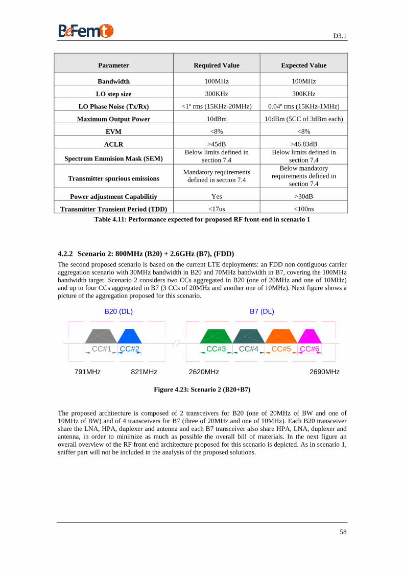
D3.1
58
Parameter Required Value Expected Value
Bandwidth 100MHz 100MHz
LO step size 300KHz 300KHz
LO Phase Noise (Tx/Rx) <1º rms (15KHz-20MHz) 0.04º rms (15KHz-1MHz)
Maximum Output Power 10dBm 10dBm (5CC of 3dBm each)
EVM <8% <8%
ACLR >45dB >46.83dB
Spectrum Emmision Mask (SEM) Below limits defined in
section 7.4 Below limits defined in
section 7.4
Transmitter spurious emissions Mandatory requirements
defined in section 7.4
Below mandatory requirements defined in
section 7.4
Power adjustment Capabilitiy Yes >30dB
Transmitter Transient Period (TDD) <17us <100ns
Table 4.11: Performance expected for proposed RF front-end in scenario 1
4.2.2 Scenario 2: 800MHz (B20) + 2.6GHz (B7), (FDD) The second proposed scenario is based on the current LTE deployments: an FDD non contiguous carrier aggregation scenario with 30MHz bandwidth in B20 and 70MHz bandwidth in B7, covering the 100MHz bandwidth target. Scenario 2 considers two CCs aggregated in B20 (one of 20MHz and one of 10MHz) and up to four CCs aggregated in B7 (3 CCs of 20MHz and another one of 10MHz). Next figure shows a picture of the aggregation proposed for this scenario.
B20 (DL)
CC#2CC#1
B7 (DL)
CC#4CC#3 CC#5
791MHz 821MHz
CC#6
2620MHz 2690MHz
Figure 4.23: Scenario 2 (B20+B7)
The proposed architecture is composed of 2 transceivers for B20 (one of 20MHz of BW and one of 10MHz of BW) and of 4 transceivers for B7 (three of 20MHz and one of 10MHz). Each B20 transceiver share the LNA, HPA, duplexer and antenna and each B7 transceiver also share HPA, LNA, duplexer and antenna, in order to minimize as much as possible the overall bill of materials. In the next figure an overall overview of the RF front-end architecture proposed for this scenario is depicted. As in scenario 1, sniffer part will not be included in the analysis of the proposed solutions.
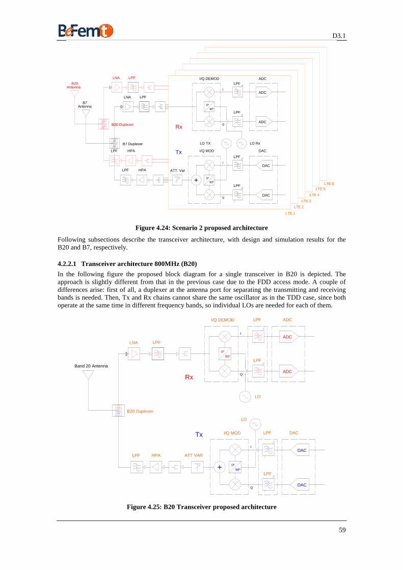
D3.1
59
LTE 4Q
DAC
LTE 1
LTE 2
LTE 3
Tx
Rx
ATT. Var
B7Antenna
LPF HPA
B7 Duplexer
LPFLNAADC
LO TX
I/Q MOD
90º+ 0º
LPF
I
LPF
90º0º
Q
LPF
DAC
DAC
ADC
I/Q DEMOD
I
LPFADC
LTE 5
LO Rx
AntennaB20
LPF HPA
B20 Duplexer
LPFLNA
LTE 6
Figure 4.24: Scenario 2 proposed architecture
Following subsections describe the transceiver architecture, with design and simulation results for the B20 and B7, respectively.
4.2.2.1 Transceiver architecture 800MHz (B20)
In the following figure the proposed block diagram for a single transceiver in B20 is depicted. The approach is slightly different from that in the previous case due to the FDD access mode. A couple of differences arise: first of all, a duplexer at the antenna port for separating the transmitting and receiving bands is needed. Then, Tx and Rx chains cannot share the same oscillator as in the TDD case, since both operate at the same time in different frequency bands, so individual LOs are needed for each of them.
LPF+
Q
0º90º
DAC
ATT VAR
Rx
Band 20 Antenna
HPALPF
B20 Duplexer
LPFLNA
0º
LPF
LO
I/Q MODTx
I
LO
90º
Q
LPF
DAC
ADC
I/Q DEMOD
I
LPF
ADC
ADC
DAC
Figure 4.25: B20 Transceiver proposed architecture
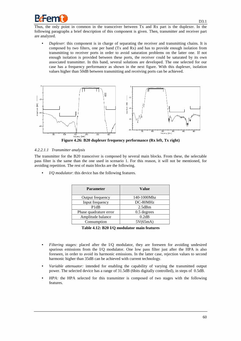
D3.1
60
Thus, the only point in common in the transceiver between Tx and Rx part is the duplexer. In the following paragraphs a brief description of this component is given. Then, transmitter and receiver part are analyzed.
• Duplexer: this component is in charge of separating the receiver and transmitting chains. It is composed by two filters, one per band (Tx and Rx) and has to provide enough isolation from transmitting to receiver ports in order to avoid saturation problems on the latter one. If not enough isolation is provided between these ports, the receiver could be saturated by its own associated transmitter. In this band, several solutions are developed. The one selected for our case has a frequency performance as shown in the next figure. With this duplexer, isolation values higher than 50dB between transmitting and receiving ports can be achieved.
Figure 4.26: B20 duplexer frequency performance (Rx left, Tx right)
4.2.2.1.1 Transmitter analysis
The transmitter for the B20 transceiver is composed by several main blocks. From these, the selectable pass filter is the same than the one used in scenario 1. For this reason, it will not be mentioned, for avoiding repetition. The rest of main blocks are the following.
• I/Q modulator: this device has the following features.
Parameter Value
Output frequency 140-1000Mhz Input frequency DC-80MHz
P1dB 2.5dBm Phase quadrature error 0.5 degrees
Amplitude balance 0.2dB Consumption 5V(65mA)
Table 4.12: B20 I/Q modulator main features
• Filtering stages: placed after the I/Q modulator, they are foreseen for avoiding undesired spurious emissions from the I/Q modulator. One low pass filter just after the HPA is also foreseen, in order to avoid its harmonic emissions. In the latter case, rejection values to second harmonic higher than 35dB can be achieved with current technology.
• Variable attenuator: intended for enabling the capability of varying the transmitted output power. The selected device has a range of 31.5dB (6bits digitally controlled), in steps of 0.5dB.
• HPA: the HPA selected for this transmitter is composed of two stages with the following features.
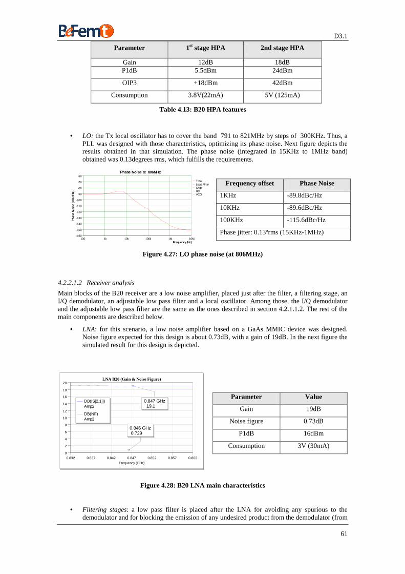
D3.1
61
Parameter 1st stage HPA 2nd stage HPA
Gain 12dB 18dB P1dB 5.5dBm 24dBm
OIP3 +18dBm 42dBm
Consumption 3.8V(22mA) 5V (125mA)
Table 4.13: B20 HPA features
• LO: the Tx local oscillator has to cover the band 791 to 821MHz by steps of 300KHz. Thus, a PLL was designed with those characteristics, optimizing its phase noise. Next figure depicts the results obtained in that simulation. The phase noise (integrated in 15KHz to 1MHz band) obtained was 0.13degrees rms, which fulfills the requirements.
100 1k 10k 100k 1M 10MFrequency (Hz)
-160
-150
-140
-130
-120
-110
-100
-90
-80
-70
-60
Ph
ase
No
ise
(dB
c/H
z)
Phase Noise at 806MHz
TotalLoop FilterChipRefVCO
Frequency offset Phase Noise
1KHz -89.8dBc/Hz
10KHz -89.6dBc/Hz
100KHz -115.6dBc/Hz
Phase jitter: 0.13ºrms (15KHz-1MHz)
Figure 4.27: LO phase noise (at 806MHz)
4.2.2.1.2 Receiver analysis
Main blocks of the B20 receiver are a low noise amplifier, placed just after the filter, a filtering stage, an I/Q demodulator, an adjustable low pass filter and a local oscillator. Among those, the I/Q demodulator and the adjustable low pass filter are the same as the ones described in section 4.2.1.1.2. The rest of the main components are described below.
• LNA: for this scenario, a low noise amplifier based on a GaAs MMIC device was designed. Noise figure expected for this design is about 0.73dB, with a gain of 19dB. In the next figure the simulated result for this design is depicted.
0.832 0.837 0.842 0.847 0.852 0.857 0.862Frequency (GHz)
LNA B20 (Gain & Noise Figure)
0
2
4
6
8
10
12
14
16
18
20
0.846 GHz 0.729
0.847 GHz 19.1
DB(|S[2,1]|)Amp2
DB(NF)Amp2
Parameter Value
Gain 19dB
Noise figure 0.73dB
P1dB 16dBm
Consumption 3V (30mA)
Figure 4.28: B20 LNA main characteristics
• Filtering stages: a low pass filter is placed after the LNA for avoiding any spurious to the demodulator and for blocking the emission of any undesired product from the demodulator (from
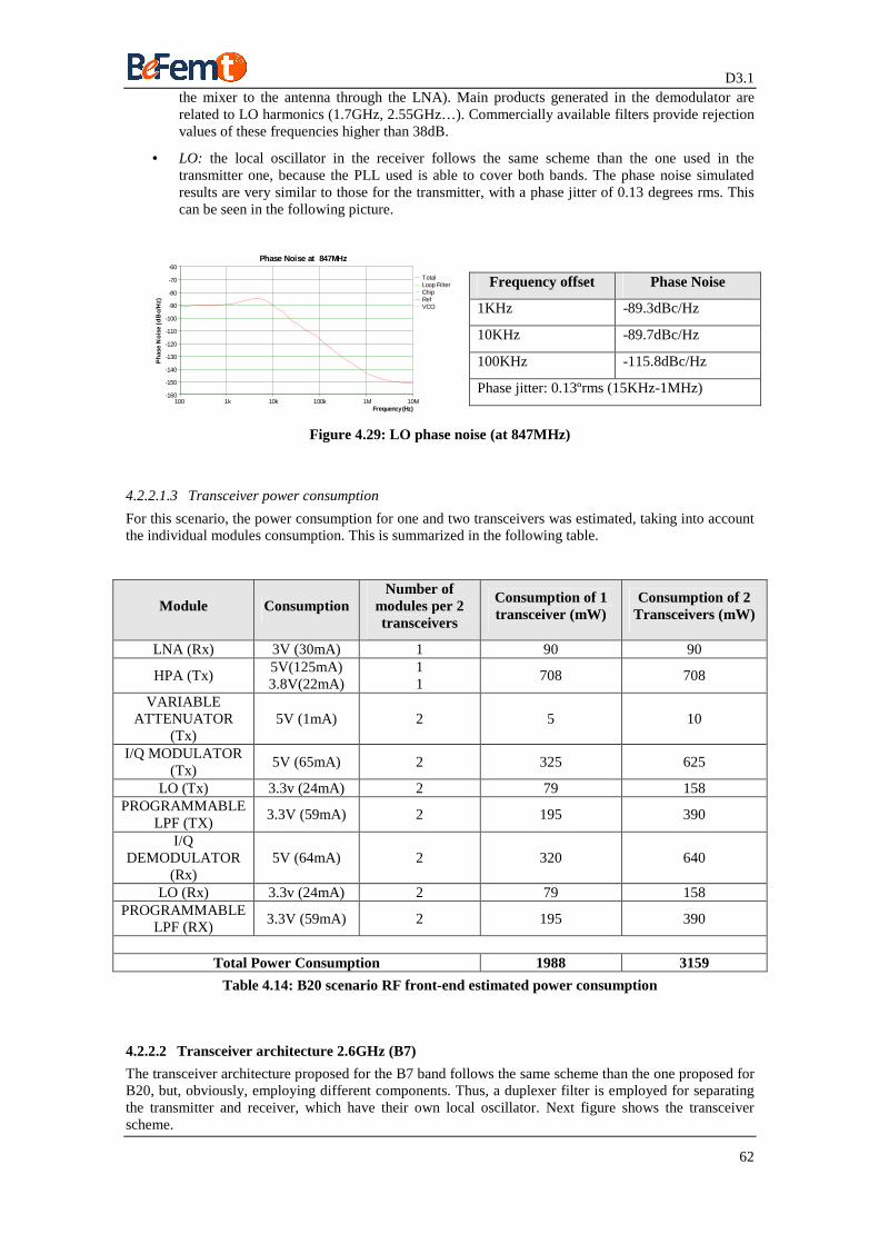
D3.1
62
the mixer to the antenna through the LNA). Main products generated in the demodulator are related to LO harmonics (1.7GHz, 2.55GHz…). Commercially available filters provide rejection values of these frequencies higher than 38dB.
• LO: the local oscillator in the receiver follows the same scheme than the one used in the transmitter one, because the PLL used is able to cover both bands. The phase noise simulated results are very similar to those for the transmitter, with a phase jitter of 0.13 degrees rms. This can be seen in the following picture.
100 1k 10k 100k 1M 10MFrequency (Hz)
-160
-150
-140
-130
-120
-110
-100
-90
-80
-70
-60
Ph
ase
No
ise
(dB
c/H
z)
Phase Noise at 847MHz
TotalLoop FilterChipRefVCO
Frequency offset Phase Noise
1KHz -89.3dBc/Hz
10KHz -89.7dBc/Hz
100KHz -115.8dBc/Hz
Phase jitter: 0.13ºrms (15KHz-1MHz)
Figure 4.29: LO phase noise (at 847MHz)
4.2.2.1.3 Transceiver power consumption
For this scenario, the power consumption for one and two transceivers was estimated, taking into account the individual modules consumption. This is summarized in the following table.
Module Consumption Number of
modules per 2 transceivers
Consumption of 1 transceiver (mW)
Consumption of 2 Transceivers (mW)
LNA (Rx) 3V (30mA) 1 90 90
HPA (Tx) 5V(125mA) 3.8V(22mA)
1 1
708 708
VARIABLE ATTENUATOR
(Tx) 5V (1mA) 2 5 10
I/Q MODULATOR (Tx)
5V (65mA) 2 325 625
LO (Tx) 3.3v (24mA) 2 79 158 PROGRAMMABLE
LPF (TX) 3.3V (59mA) 2 195 390
I/Q DEMODULATOR
(Rx) 5V (64mA) 2 320 640
LO (Rx) 3.3v (24mA) 2 79 158 PROGRAMMABLE
LPF (RX) 3.3V (59mA) 2 195 390
Total Power Consumption 1988 3159
Table 4.14: B20 scenario RF front-end estimated power consumption
4.2.2.2 Transceiver architecture 2.6GHz (B7)
The transceiver architecture proposed for the B7 band follows the same scheme than the one proposed for B20, but, obviously, employing different components. Thus, a duplexer filter is employed for separating the transmitter and receiver, which have their own local oscillator. Next figure shows the transceiver scheme.
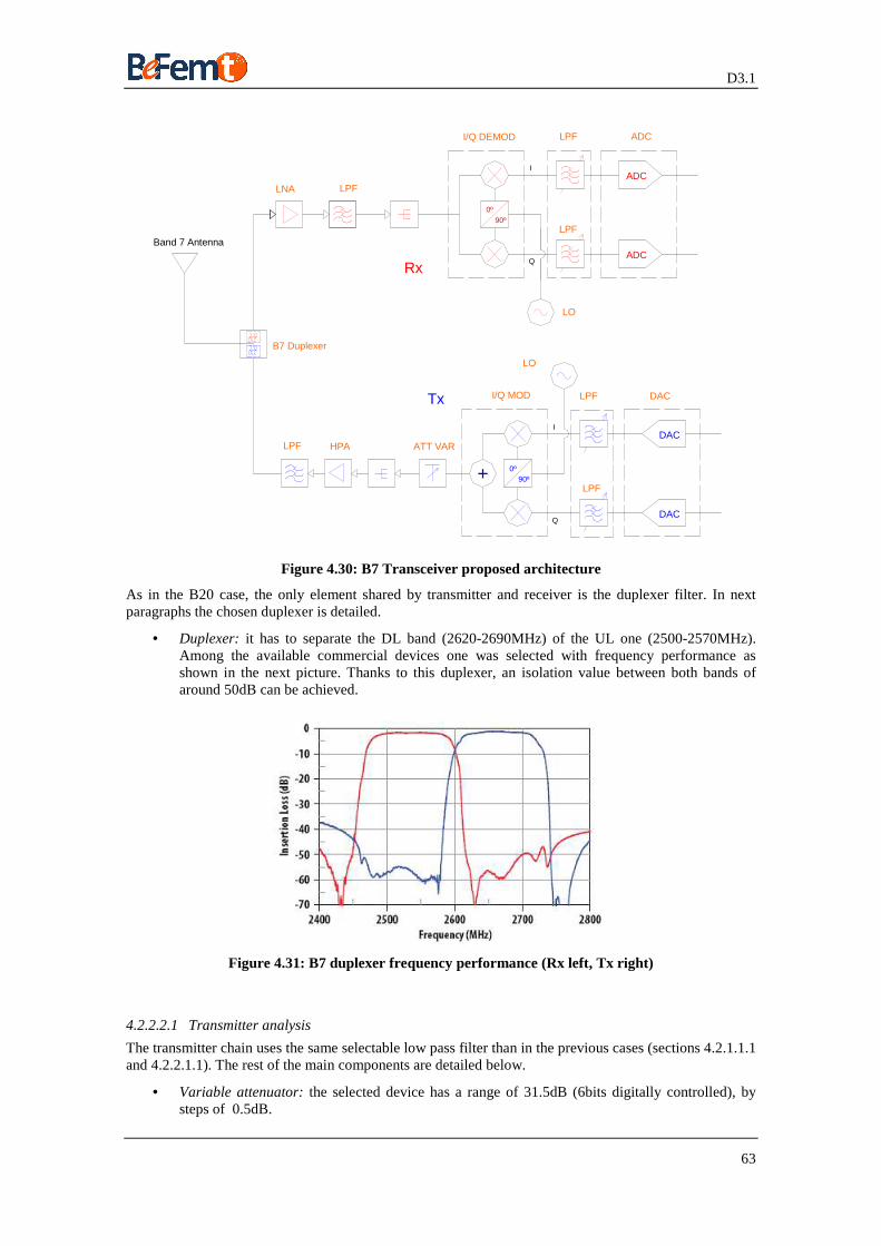
D3.1
63
Rx
LPFLNAADC
LO
90º0º
Q
LPF
ADC
I
LPF
QDAC
HPA ATT VAR
90º+ 0º
LPF
IDAC
Tx I/Q MOD
I/Q DEMOD
LPF
LO
LPF
B7 Duplexer
Band 7 Antenna
ADC
DAC
Figure 4.30: B7 Transceiver proposed architecture
As in the B20 case, the only element shared by transmitter and receiver is the duplexer filter. In next paragraphs the chosen duplexer is detailed.
• Duplexer: it has to separate the DL band (2620-2690MHz) of the UL one (2500-2570MHz). Among the available commercial devices one was selected with frequency performance as shown in the next picture. Thanks to this duplexer, an isolation value between both bands of around 50dB can be achieved.
Figure 4.31: B7 duplexer frequency performance (Rx left, Tx right)
4.2.2.2.1 Transmitter analysis
The transmitter chain uses the same selectable low pass filter than in the previous cases (sections 4.2.1.1.1 and 4.2.2.1.1). The rest of the main components are detailed below.
• Variable attenuator: the selected device has a range of 31.5dB (6bits digitally controlled), by steps of 0.5dB.
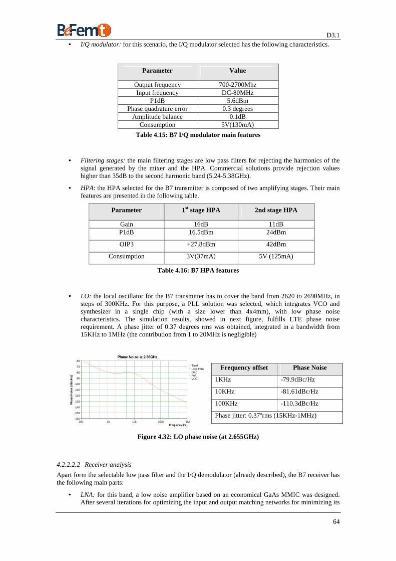
D3.1
64
• I/Q modulator: for this scenario, the I/Q modulator selected has the following characteristics.
Parameter Value
Output frequency 700-2700Mhz Input frequency DC-80MHz
P1dB 5.6dBm Phase quadrature error 0.3 degrees
Amplitude balance 0.1dB Consumption 5V(130mA)
Table 4.15: B7 I/Q modulator main features
• Filtering stages: the main filtering stages are low pass filters for rejecting the harmonics of the signal generated by the mixer and the HPA. Commercial solutions provide rejection values higher than 35dB to the second harmonic band (5.24-5.38GHz).
• HPA: the HPA selected for the B7 transmitter is composed of two amplifying stages. Their main features are presented in the following table.
Parameter 1st stage HPA 2nd stage HPA
Gain 16dB 11dB P1dB 16.5dBm 24dBm
OIP3 +27.8dBm 42dBm
Consumption 3V(37mA) 5V (125mA)
Table 4.16: B7 HPA features
• LO: the local oscillator for the B7 transmitter has to cover the band from 2620 to 2690MHz, in steps of 300KHz. For this purpose, a PLL solution was selected, which integrates VCO and synthesizer in a single chip (with a size lower than 4x4mm), with low phase noise characteristics. The simulation results, showed in next figure, fulfills LTE phase noise requirement. A phase jitter of 0.37 degrees rms was obtained, integrated in a bandwidth from 15KHz to 1MHz (the contribution from 1 to 20MHz is negligible)
100 1k 10k 100k 1MFrequency (Hz)
-160
-150
-140
-130
-120
-110
-100
-90
-80
-70
-60
Ph
ase
No
ise
(dB
c/H
z)
Phase Noise at 2.66GHz
TotalLoop FilterChipRefVCO
Frequency offset Phase Noise
1KHz -79.9dBc/Hz
10KHz -81.61dBc/Hz
100KHz -110.3dBc/Hz
Phase jitter: 0.37ºrms (15KHz-1MHz)
Figure 4.32: LO phase noise (at 2.655GHz)
4.2.2.2.2 Receiver analysis
Apart form the selectable low pass filter and the I/Q demodulator (already described), the B7 receiver has the following main parts:
• LNA: for this band, a low noise amplifier based on an economical GaAs MMIC was designed. After several iterations for optimizing the input and output matching networks for minimizing its
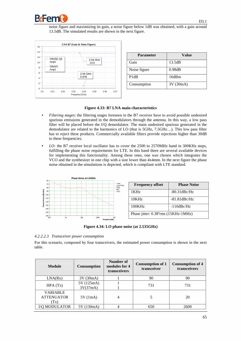
D3.1
65
noise figure and maximizing its gain, a noise figure below 1dB was obtained, with a gain around 13.5dB. The simulated results are shown in the next figure.
2.5 2.51 2.52 2.53 2.54 2.55 2.56 2.57
Frequency (GHz)
LNA B7 (Gain & Noise Figure)
0
2
4
6
8
10
12
14
16
2.54 GHz 0.978
2.54 GHz 13.5
DB(|S[2,1]|)Amp2
DB(NF)Amp2
Parameter Value
Gain 13.5dB
Noise figure 0.98dB
P1dB 16dBm
Consumption 3V (30mA)
Figure 4.33: B7 LNA main characteristics
• Filtering stages: the filtering stages foreseen in the B7 receiver have to avoid possible undesired spurious emissions generated in the demodulators through the antenna. In this way, a low pass filter will be placed before the I/Q demodulator. The main undesired spurious generated in the demodulator are related to the harmonics of LO (that is 5GHz, 7.5GHz…). This low pass filter has to reject these products. Commercially available filters provide rejections higher than 30dB to these frequencies.
• LO: the B7 receiver local oscillator has to cover the 2500 to 2570MHz band in 300KHz steps, fulfilling the phase noise requirements for LTE. In this band there are several available devices for implementing this functionality. Among these ones, one was chosen which integrates the VCO and the synthesizer in one chip with a size lower than 4x4mm. In the next figure the phase noise obtained in the simulations is depicted, which is compliant with LTE standard.
100 1k 10k 100k 1MFrequency (Hz)
-160
-150
-140
-130
-120
-110
-100
-90
-80
-70
-60
Ph
ase
No
ise
(dB
c/H
z)
Phase Noise at 2.54GHz
TotalLoop FilterChipRefVCO
Frequency offset Phase Noise
1KHz -80.31dBc/Hz
10KHz -81.81dBc/Hz
100KHz -110dBc/Hz
Phase jitter: 0.38ºrms (15KHz-1MHz)
Figure 4.34: LO phase noise (at 2.535GHz)
4.2.2.2.3 Transceiver power consumption
For this scenario, composed by four transceivers, the estimated power consumption is shown in the next table.
Module Consumption Number of
modules for 4 transceivers
Consumption of 1 transceiver
Consumption of 4 transceivers
LNA(Rx) 3V (30mA) 1 90 90
HPA (Tx) 5V (125mA) 3V(37mA)
1 1
731 731
VARIABLE ATTENUATOR
(Tx) 5V (1mA) 4 5 20
I/Q MODULATOR 5V (130mA) 4 650 2600
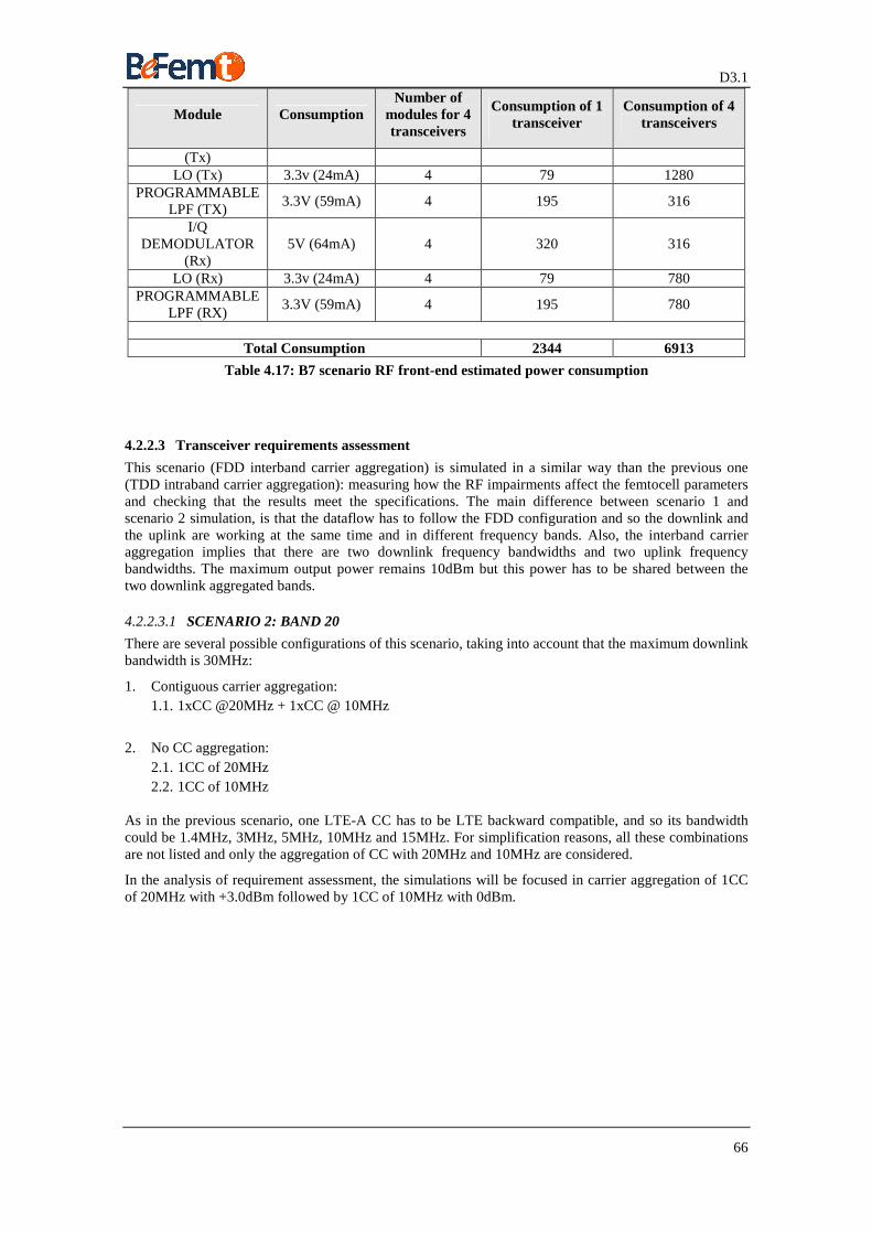
D3.1
66
Module Consumption Number of
modules for 4 transceivers
Consumption of 1 transceiver
Consumption of 4 transceivers
(Tx) LO (Tx) 3.3v (24mA) 4 79 1280
PROGRAMMABLE LPF (TX)
3.3V (59mA) 4 195 316
I/Q DEMODULATOR
(Rx) 5V (64mA) 4 320 316
LO (Rx) 3.3v (24mA) 4 79 780 PROGRAMMABLE
LPF (RX) 3.3V (59mA) 4 195 780
Total Consumption 2344 6913
Table 4.17: B7 scenario RF front-end estimated power consumption
4.2.2.3 Transceiver requirements assessment
This scenario (FDD interband carrier aggregation) is simulated in a similar way than the previous one (TDD intraband carrier aggregation): measuring how the RF impairments affect the femtocell parameters and checking that the results meet the specifications. The main difference between scenario 1 and scenario 2 simulation, is that the dataflow has to follow the FDD configuration and so the downlink and the uplink are working at the same time and in different frequency bands. Also, the interband carrier aggregation implies that there are two downlink frequency bandwidths and two uplink frequency bandwidths. The maximum output power remains 10dBm but this power has to be shared between the two downlink aggregated bands.
4.2.2.3.1 SCENARIO 2: BAND 20
There are several possible configurations of this scenario, taking into account that the maximum downlink bandwidth is 30MHz:
1. Contiguous carrier aggregation: 1.1. 1xCC @20MHz + 1xCC @ 10MHz
2. No CC aggregation:
2.1. 1CC of 20MHz 2.2. 1CC of 10MHz
As in the previous scenario, one LTE-A CC has to be LTE backward compatible, and so its bandwidth could be 1.4MHz, 3MHz, 5MHz, 10MHz and 15MHz. For simplification reasons, all these combinations are not listed and only the aggregation of CC with 20MHz and 10MHz are considered.
In the analysis of requirement assessment, the simulations will be focused in carrier aggregation of 1CC of 20MHz with +3.0dBm followed by 1CC of 10MHz with 0dBm.
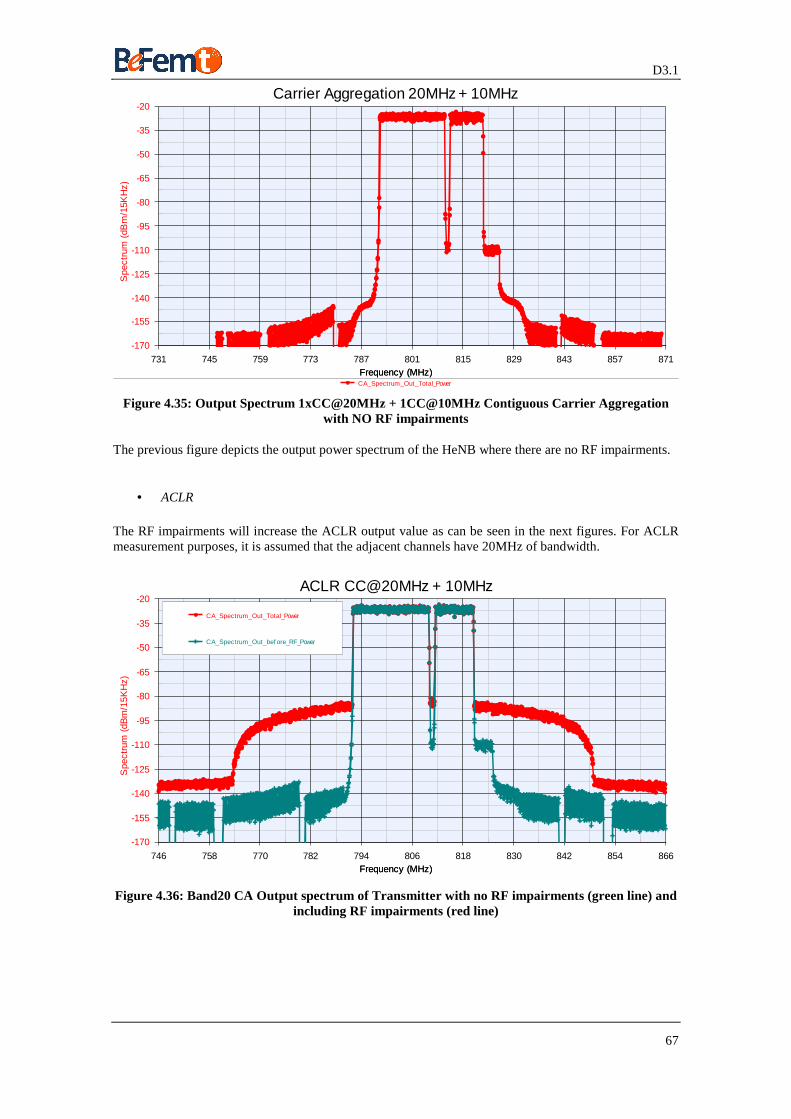
D3.1
67
Frequency (MHz)
Spe
ctru
m (
dBm
/15K
Hz)
-170
-155
-140
-125
-110
-95
-80
-65
-50
-35
-20
Frequency (MHz)731 745 759 773 787 801 815 829 843 857 871
Carrier Aggregation 20MHz + 10MHz
CA_Spectrum_Out_Total_Power
Figure 4.35: Output Spectrum 1xCC@20MHz + 1CC@10MHz Contiguous Carrier Aggregation with NO RF impairments
The previous figure depicts the output power spectrum of the HeNB where there are no RF impairments.
• ACLR
The RF impairments will increase the ACLR output value as can be seen in the next figures. For ACLR measurement purposes, it is assumed that the adjacent channels have 20MHz of bandwidth.
Frequency (MHz)
Spe
ctru
m (
dBm
/15K
Hz)
-170
-155
-140
-125
-110
-95
-80
-65
-50
-35
-20
Frequency (MHz)746 758 770 782 794 806 818 830 842 854 866
ACLR CC@20MHz + 10MHz
CA_Spectrum_Out_Total_Power
CA_Spectrum_Out_bef ore_RF_Power
Figure 4.36: Band20 CA Output spectrum of Transmitter with no RF impairments (green line) and including RF impairments (red line)
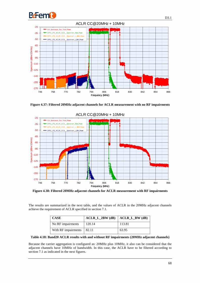
D3.1
68
Frequency (MHz)
Spe
ctru
m (
dBm
/15K
Hz)
-170
-155
-140
-125
-110
-95
-80
-65
-50
-35
-20
Frequency (MHz)746 758 770 782 794 806 818 830 842 854 866
ACLR CC@20MHz + 10MHzCA_Spectrum_Out_Total_Power
DPD_LTE_ACLR_CC3__Spectrum_Main_Power
DPD_LTE_ACLR_CC3__Spectrum_L_2BW_Power
DPD_LTE_ACLR_CC3__Spectrum_L_BW_Power
Figure 4.37: Filtered 20MHz adjacent channels for ACLR measurement with no RF impairments
Frequency (MHz)
Spe
ctru
m (
dBm
/15K
Hz)
-170
-155
-140
-125
-110
-95
-80
-65
-50
-35
-20
Frequency (MHz)746 758 770 782 794 806 818 830 842 854 866
ACLR CC@20MHz + 10MHzCA_Spectrum_Out_Total_Power
DPD_LTE_ACLR_CC3__Spectrum_Main_Power
DPD_LTE_ACLR_CC3__Spectrum_L_2BW_Power
DPD_LTE_ACLR_CC3__Spectrum_L_BW_Power
Figure 4.38: Filtered 20MHz adjacent channels for ACLR measurement with RF impairments
The results are summarized in the next table, and the values of ACLR in the 20MHz adjacent channels achieve the requirement of ACLR specified in section 7.1.
CASE ACLR_L_2BW (dB) ACLR_L_BW (dB)
No RF impairments 120.14 113.81
With RF impairments 82.11 63.95
Table 4.18: Band20 ACLR results with and without RF impairments (20MHz adjacent channels)
Because the carrier aggregation is configured as: 20MHz plus 10MHz, it also can be considered that the adjacent channels have 10MHz of bandwidth. In this case, the ACLR have to be filtered according to section 7.1 as indicated in the next figures.
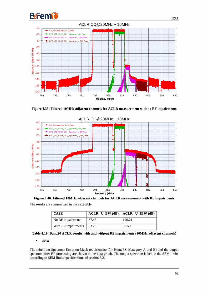
D3.1
69
Frequency (MHz)
Spe
ctru
m (
dBm
/15K
Hz)
-170
-155
-140
-125
-110
-95
-80
-65
-50
-35
-20
Frequency (MHz)746 758 770 782 794 806 818 830 842 854 866
ACLR CC@20MHz + 10MHzCA_Spectrum_Out_Total_Power
DPD_LTE_ACLR_CC3__Spectrum_Main_Power
DPD_LTE_ACLR_CC3__Spectrum_U_BW_Power
DPD_LTE_ACLR_CC3__Spectrum_U_2BW_Power
Figure 4.39: Filtered 10MHz adjacent channels for ACLR measurement with no RF impairments
Frequency (MHz)
Spe
ctru
m (
dBm
/15K
Hz)
-170
-155
-140
-125
-110
-95
-80
-65
-50
-35
-20
Frequency (MHz)746 758 770 782 794 806 818 830 842 854 866
ACLR CC@20MHz + 10MHzCA_Spectrum_Out_Total_Power
DPD_LTE_ACLR_CC3__Spectrum_Main_Power
DPD_LTE_ACLR_CC3__Spectrum_U_BW_Power
DPD_LTE_ACLR_CC3__Spectrum_U_2BW_Power
Figure 4.40: Filtered 10MHz adjacent channels for ACLR measurement with RF impairments
The results are summarized in the next table.
CASE ACLR _U_BW (dB) ACLR _U_2BW (dB)
No RF impairments 87.43 120.21
With RF impairments 63.28 67.50
Table 4.19: Band20 ACLR results with and without RF impairments (10MHz adjacent channels)
• SEM
The minimum Spectrum Emission Mask requirements for HomeBS (Category A and B) and the output spectrum after RF processing are shown in the next graph. The output spectrum is below the SEM limits according to SEM limits specifications of section 7.2.
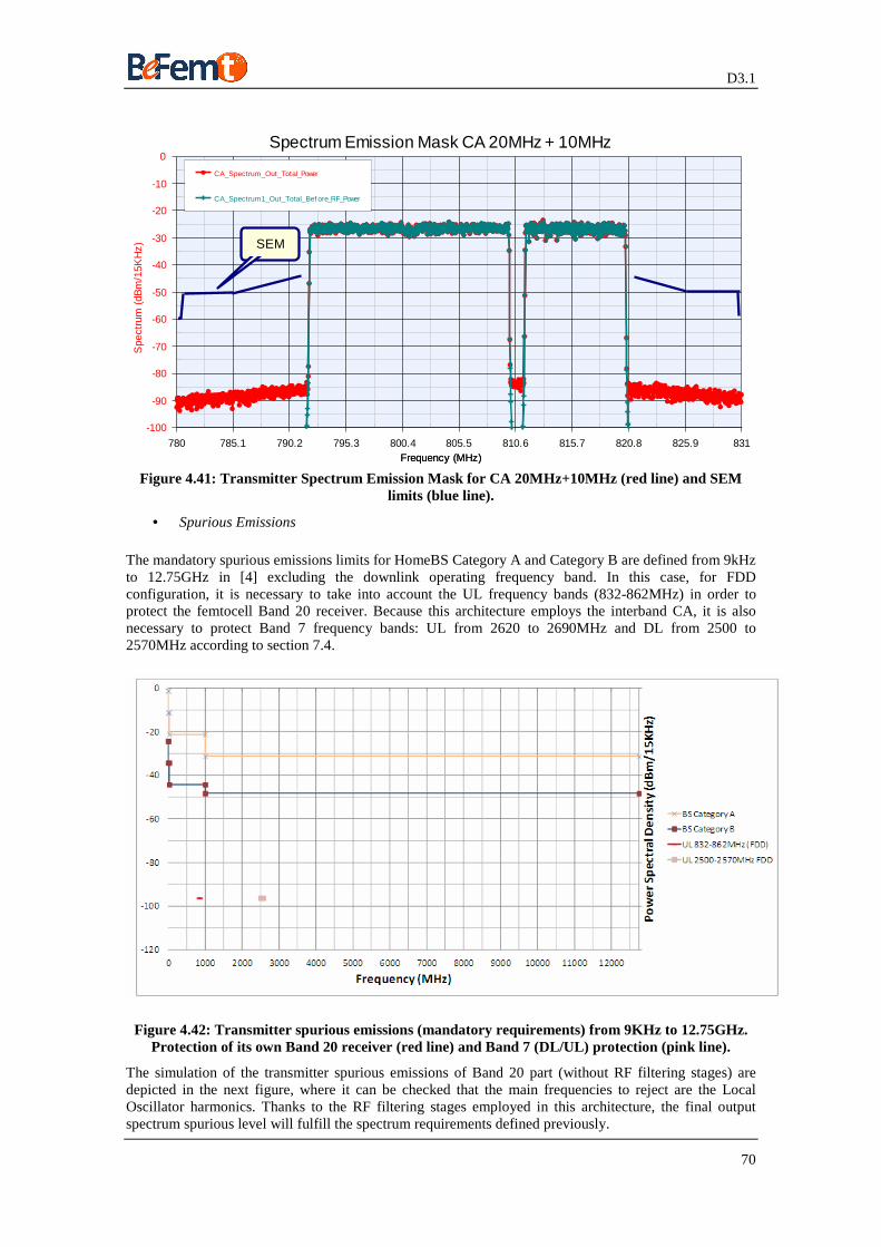
D3.1
70
Frequency (MHz)
Spe
ctru
m (
dBm
/15K
Hz)
-100
-90
-80
-70
-60
-50
-40
-30
-20
-10
0
Frequency (MHz)780 785.1 790.2 795.3 800.4 805.5 810.6 815.7 820.8 825.9 831
Spectrum Emission Mask CA 20MHz + 10MHz
CA_Spectrum_Out_Total_Power
CA_Spectrum1_Out_Total_Bef ore_RF_Power
SEM
Figure 4.41: Transmitter Spectrum Emission Mask for CA 20MHz+10MHz (red line) and SEM
limits (blue line).
• Spurious Emissions
The mandatory spurious emissions limits for HomeBS Category A and Category B are defined from 9kHz to 12.75GHz in [4] excluding the downlink operating frequency band. In this case, for FDD configuration, it is necessary to take into account the UL frequency bands (832-862MHz) in order to protect the femtocell Band 20 receiver. Because this architecture employs the interband CA, it is also necessary to protect Band 7 frequency bands: UL from 2620 to 2690MHz and DL from 2500 to 2570MHz according to section 7.4.
Figure 4.42: Transmitter spurious emissions (mandatory requirements) from 9KHz to 12.75GHz. Protection of its own Band 20 receiver (red line) and Band 7 (DL/UL) protection (pink line).
The simulation of the transmitter spurious emissions of Band 20 part (without RF filtering stages) are depicted in the next figure, where it can be checked that the main frequencies to reject are the Local Oscillator harmonics. Thanks to the RF filtering stages employed in this architecture, the final output spectrum spurious level will fulfill the spectrum requirements defined previously.
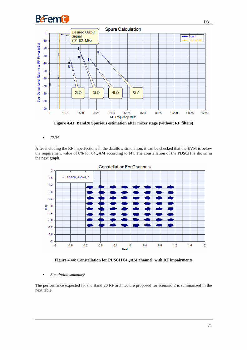
D3.1
71
Figure 4.43: Band20 Spurious estimation after mixer stage (without RF filters)
• EVM
After including the RF imperfections in the dataflow simulation, it can be checked that the EVM is below the requirement value of 8% for 64QAM according to [4]. The constellation of the PDSCH is shown in the next graph.
Figure 4.44: Constellation for PDSCH 64QAM channel, with RF impairments
• Simulation summary
The performance expected for the Band 20 RF architecture proposed for scenario 2 is summarized in the next table.
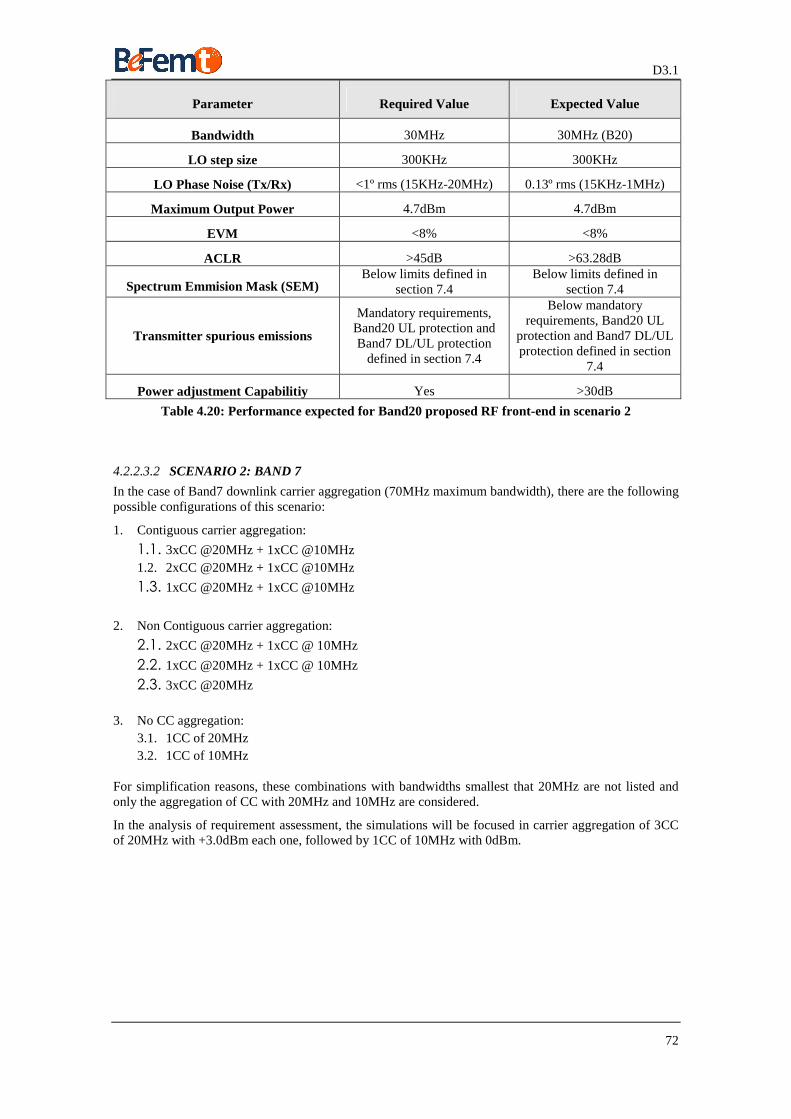
D3.1
72
Parameter Required Value Expected Value
Bandwidth 30MHz 30MHz (B20)
LO step size 300KHz 300KHz
LO Phase Noise (Tx/Rx) <1º rms (15KHz-20MHz) 0.13º rms (15KHz-1MHz)
Maximum Output Power 4.7dBm 4.7dBm
EVM <8% <8%
ACLR >45dB >63.28dB
Spectrum Emmision Mask (SEM) Below limits defined in
section 7.4 Below limits defined in
section 7.4
Transmitter spurious emissions
Mandatory requirements, Band20 UL protection and Band7 DL/UL protection
defined in section 7.4
Below mandatory requirements, Band20 UL
protection and Band7 DL/UL protection defined in section
7.4
Power adjustment Capabilitiy Yes >30dB
Table 4.20: Performance expected for Band20 proposed RF front-end in scenario 2
4.2.2.3.2 SCENARIO 2: BAND 7
In the case of Band7 downlink carrier aggregation (70MHz maximum bandwidth), there are the following possible configurations of this scenario:
1. Contiguous carrier aggregation:
1.1. 3xCC @20MHz + 1xCC @10MHz
1.2. 2xCC @20MHz + 1xCC @10MHz
1.3. 1xCC @20MHz + 1xCC @10MHz
2. Non Contiguous carrier aggregation:
2.1. 2xCC @20MHz + 1xCC @ 10MHz
2.2. 1xCC @20MHz + 1xCC @ 10MHz
2.3. 3xCC @20MHz 3. No CC aggregation:
3.1. 1CC of 20MHz 3.2. 1CC of 10MHz
For simplification reasons, these combinations with bandwidths smallest that 20MHz are not listed and only the aggregation of CC with 20MHz and 10MHz are considered.
In the analysis of requirement assessment, the simulations will be focused in carrier aggregation of 3CC of 20MHz with +3.0dBm each one, followed by 1CC of 10MHz with 0dBm.
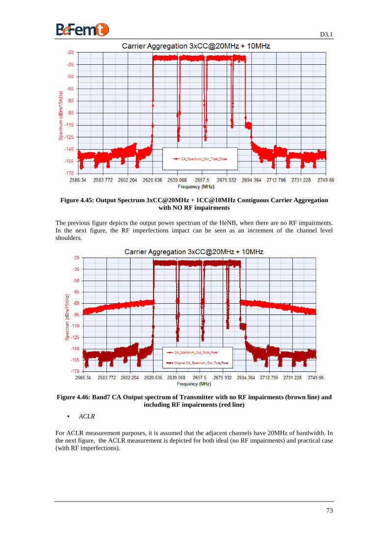
D3.1
73
Figure 4.45: Output Spectrum 3xCC@20MHz + 1CC@10MHz Contiguous Carrier Aggregation with NO RF impairments
The previous figure depicts the output power spectrum of the HeNB, when there are no RF impairments. In the next figure, the RF imperfections impact can be seen as an increment of the channel level shoulders.
Figure 4.46: Band7 CA Output spectrum of Transmitter with no RF impairments (brown line) and including RF impairments (red line)
• ACLR
For ACLR measurement purposes, it is assumed that the adjacent channels have 20MHz of bandwidth. In the next figure, the ACLR measurement is depicted for both ideal (no RF impairments) and practical case (with RF imperfections).
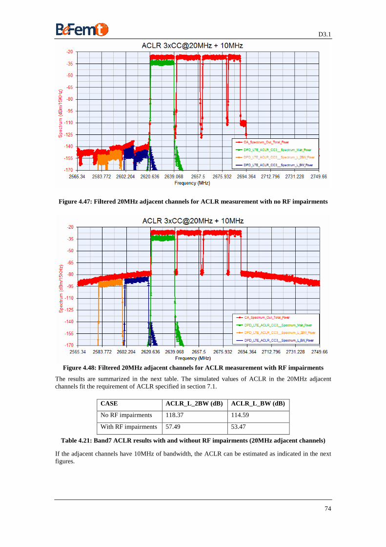
D3.1
74
Figure 4.47: Filtered 20MHz adjacent channels for ACLR measurement with no RF impairments
Figure 4.48: Filtered 20MHz adjacent channels for ACLR measurement with RF impairments
The results are summarized in the next table. The simulated values of ACLR in the 20MHz adjacent channels fit the requirement of ACLR specified in section 7.1.
CASE ACLR_L_2BW (dB) ACLR_L_BW (dB)
No RF impairments 118.37 114.59
With RF impairments 57.49 53.47
Table 4.21: Band7 ACLR results with and without RF impairments (20MHz adjacent channels)
If the adjacent channels have 10MHz of bandwidth, the ACLR can be estimated as indicated in the next figures.
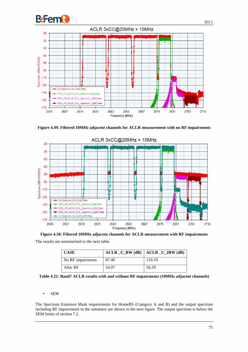
D3.1
75
Figure 4.49: Filtered 10MHz adjacent channels for ACLR measurement with no RF impairments
Figure 4.50: Filtered 10MHz adjacent channels for ACLR measurement with RF impairments
The results are summarized in the next table.
CASE ACLR _U_BW (dB) ACLR _U_2BW (dB)
No RF impairments 87.40 119.19
After RF 54.97 56.59
Table 4.22: Band7 ACLR results with and without RF impairments (10MHz adjacent channels)
• SEM
The Spectrum Emission Mask requirements for HomeBS (Category A and B) and the output spectrum including RF impairments in the simulator are shown in the next figure. The output spectrum is below the SEM limits of section 7.2.
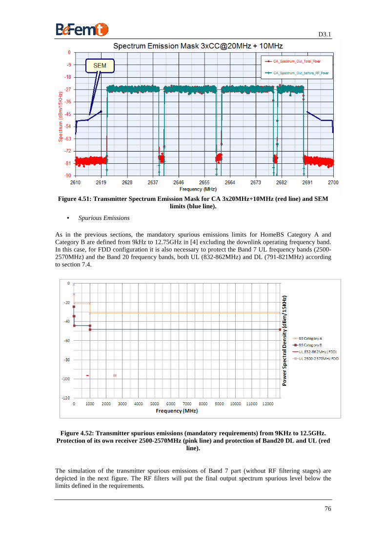
D3.1
76
Figure 4.51: Transmitter Spectrum Emission Mask for CA 3x20MHz+10MHz (red line) and SEM
limits (blue line).
• Spurious Emissions
As in the previous sections, the mandatory spurious emissions limits for HomeBS Category A and Category B are defined from 9kHz to 12.75GHz in [4] excluding the downlink operating frequency band. In this case, for FDD configuration it is also necessary to protect the Band 7 UL frequency bands (2500-2570MHz) and the Band 20 frequency bands, both UL (832-862MHz) and DL (791-821MHz) according to section 7.4.
Figure 4.52: Transmitter spurious emissions (mandatory requirements) from 9KHz to 12.5GHz. Protection of its own receiver 2500-2570MHz (pink line) and protection of Band20 DL and UL (red
line).
The simulation of the transmitter spurious emissions of Band 7 part (without RF filtering stages) are depicted in the next figure. The RF filters will put the final output spectrum spurious level below the limits defined in the requirements.
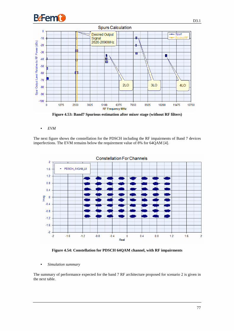
D3.1
77
Figure 4.53: Band7 Spurious estimation after mixer stage (without RF filters)
• EVM
The next figure shows the constellation for the PDSCH including the RF impairments of Band 7 devices imperfections. The EVM remains below the requirement value of 8% for 64QAM [4].
Figure 4.54: Constellation for PDSCH 64QAM channel, with RF impairments
• Simulation summary
The summary of performance expected for the band 7 RF architecture proposed for scenario 2 is given in the next table.
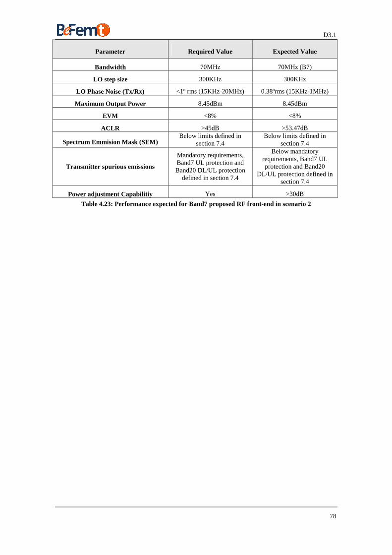
D3.1
78
Parameter Required Value Expected Value
Bandwidth 70MHz 70MHz (B7)
LO step size 300KHz 300KHz
LO Phase Noise (Tx/Rx) <1º rms (15KHz-20MHz) 0.38ºrms (15KHz-1MHz)
Maximum Output Power 8.45dBm 8.45dBm
EVM <8% <8%
ACLR >45dB >53.47dB
Spectrum Emmision Mask (SEM) Below limits defined in
section 7.4 Below limits defined in
section 7.4
Transmitter spurious emissions
Mandatory requirements, Band7 UL protection and Band20 DL/UL protection
defined in section 7.4
Below mandatory requirements, Band7 UL protection and Band20
DL/UL protection defined in section 7.4
Power adjustment Capabilitiy Yes >30dB
Table 4.23: Performance expected for Band7 proposed RF front-end in scenario 2
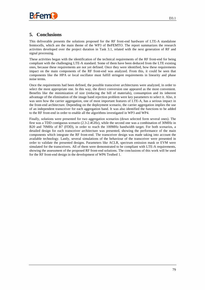
D3.1
79
5. Conclusions This deliverable presents the solutions proposed for the RF front-end hardware of LTE-A standalone femtocells, which are the main theme of the WP3 of BeFEMTO. The report summarizes the research activities developed over the project duration in Task 3.1, related with the next generation of RF and signal processing.
These activities began with the identification of the technical requirements of the RF front-end for being compliant with the challenging LTE-A standard. Some of them have been deduced from the LTE existing ones, because these requirements are not yet defined. Once they were identified, how these requirements impact on the main components of the RF front-end was analyzed. From this, it could be seen that components like the HPA or local oscillator must fulfill stringent requirements in linearity and phase noise terms.
Once the requirements had been defined, the possible transceiver architectures were analyzed, in order to select the most appropriate one. In this way, the direct conversion one appeared as the most convenient. Benefits like the minimization of size (reducing the bill of materials), consumption and its inherent advantage of the elimination of the image band rejection problem were key parameters to select it. Also, it was seen how the carrier aggregation, one of most important features of LTE-A, has a serious impact in the front-end architecture. Depending on the deployment scenario, the carrier aggregation implies the use of an independent transceiver for each aggregation band. It was also identified the functions to be added to the RF front-end in order to enable all the algorithms investigated in WP3 and WP4.
Finally, solutions were presented for two aggregation scenarios (down selected form several ones). The first was a TDD contiguous scenario (2.3-2.4GHz), while the second one was a combination of 30MHz in B20 and 70MHz of B7 (FDD), in order to reach the 100MHz bandwidth target. For both scenarios, a detailed design for each transceiver architecture was presented, showing the performance of the main components which integrate the RF front-end. The transceiver design was made taking into account the available technology. Lastly, several simulations of the behaviour of the transceiver were presented in order to validate the presented designs. Parameters like ACLR, spectrum emission mask or EVM were simulated for the transceivers. All of them were demonstrated to be compliant with LTE-A requirements, showing the assessment of the proposed RF front-end solutions. The conclusions of this work will be used for the RF front-end design in the development of WP6 Testbed 1.
D3.1
80
6. References [1] 3GPP TR 36.912 V9.3.0 (2010-06), “Feasibility study for Further Advancements for E-UTRA
(LTE-Advanced) (Release 9)”
[2] 3GPP TR 36.815 V9.1.0 (2010-06), “Further advancements for E-UTRA; LTE-Advanced feasibility studies in RAN WG4 (Release 9)”
[3] 3GPP TR 36.913 V9.0.0 (2009-12), “Requirements for further advancements for Evolved Universal Terrestrial Radio Access (E-UTRA) (LTE-Advanced) (Release 9)”
[4] 3GPP TS 36.104 V10.4.0 (2011-09) “Base Station (BS) radio transmission and reception (Release 10)”
[5] 3GPP R4-091150, "Proposals for contiguous carrier aggregation", Huawei, RAN4#50bis, Seoul, Korea, Mar. 23-27, 2009.
[6] 3GPP R4-091151, “Simulation results for contiguous carrier-aggregation”, Huawei, RAN4#50bis, Seoul, Korea, Mar. 23-27, 2009.
[7] “Phase Noise measurements for Wireless Broadband”, White Paper Nº. 11410-00456, Anritsu Application Note
[8] ITU-R Recommendation SM.328: “Spectra and bandwidth of emissions”
[9] ITU-R Recommendation SM.329-10: “Unwanted emissions in the spurious domain”
[10] 3GPP R4-091350, “Analysis of Carrier Aggregation for LTE Advanced”, Ericsson, RAN4#50bis, Seoul, Korea, Mar. 9-13, 2009.
[11] 3GPP R4-091667, “Further considerations on contiguous carrier aggregation for LTE-Advanced”, Huawei, RAN4#51, San Francisco, CA, May 4-8, 2009
[12] 3GPP R1-083704, “Downlink spectrum utilization in LTE-Advanced”, Huawei, RAN WG1 Meeting #5bis, Prague, Czech Rep, Sep29-Oct3, 2008
[13] “LTE and the Evolution to 4G Wireless, Design and Measurement Challenges”, 2009 Agilent Technologies
[14] “Adjacent Channel Leakage Ratio (ACLR) Derivation for General RF Devices”, Application Note 3902, Maxim, Sep. 2006
[15] “LTE Base Station MMIC Amplifier”, Technical Note AN-60-041, MiniCircuits.
[16] S. Sesia, I. Toufik, and M. Baker, “LTE - The UMTS Long Term Evolution: From Theory to Practice”, 1st ed., Wiley, 2009
[17] “RF transceiver Architecture for Cognitive Radio User Equipment”, End to End Reconfigurability II (E2R II) White Paper, June 2007
[18] “Direct conversion receiver designs enable multi-standard/multi-band operation”, Rakesh Soni and Eric Newman, Analog Devices, Inc., 2/16/2009
[19] “A CMOS Front end for high linearity zero-IF WCDMA Receiver”, Shaikh Md. Khairul Alam, M.S., The Ohio State University, 2006
[20] “The advantages of using a quadrature digital upconverter (QDUC) in Point-to-Point Microwave Transmit Systems”, David Brandon, David, Crook, and Ken Gentile, Analog Devices, Application Note AN-0996
[21] 3GPP TR 36.921, v10.0.0 (2011-04), “Home eNodeB (HeNB) Radio Frequency (RF) requirements analysis (Release 10)”
[22] “Introducing LTE-Advanced”, Application note 5990-6706EN, Agilent technologies, March 2011
[23] “LTE-Advanced Signal Generation and Analysis”, Application Note 1MA166, Rhode and Schwarz, February 2010
[24] “Worldwide LTE network commitments, launches and trials”, www.gsacom.com, October 2011
[25] “A global analysis of LTE spectrum requirement and business models”, Daniele Tricarito, Bogotá, August 2011
D3.1
81
[26] 3GPP TS25.104 v9.3.0 (2010-03), “Base Station (BS) radio transmission and reception (FDD) (Release 9)”
[27] 3GPP TS25.105 v10.0.0 (2010-06), “Base Station (BS) radio transmission and reception (TDD) (Release 10)”
D3.1
82
7. Appendix A: Further Information for Technical RF re quirements This appendix contains further information about some of the technical requirements included in previous sections. This information comes from [4].
7.1 Adjacent Channel Leakage power Ratio (ACLR)
Channel bandwidth of E-UTRA lowest (highest) carrier
transmitted BWChannel [MHz]
BS adjacent channel centre frequency offset below the
lowest or above the highest carrier
centre frequency transmitted
Assumed adjacent channel carrier (informative)
Filter on the adjacent channel
frequency and corresponding filter
bandwidth
ACLR limit
BWChannel E-UTRA of same BW
Square (BWConfig) 45 dB
2 x BWChannel E-UTRA of same BW
Square (BWConfig) 45 dB
BWChannel /2 + 2.5 MHz
3.84 Mcps UTRA RRC (3.84 Mcps) 45 dB
1.4, 3.0, 5, 10, 15, 20
BWChannel /2 + 7.5 MHz
3.84 Mcps UTRA RRC (3.84 Mcps) 45 dB
NOTE 1: BWChannel and BWConfig are the channel bandwidth and transmission bandwidth configuration of the E-UTRA lowest (highest) carrier transmitted on the assigned channel frequency. NOTE 2: The RRC filter shall be equivalent to the transmit pulse shape filter defined in [26], with a chip rate as defined in this table.
Table 7.1: Base Station ACLR in paired spectrum
Channel bandwidth of E-UTRA lowest (highest) carrier
transmitted BWChannel [MHz]
BS adjacent channel centre frequency offset below the
lowest or above the highest carrier
centre frequency transmitted
Assumed adjacent channel carrier (informative)
Filter on the adjacent channel frequency and
corresponding filter bandwidth
ACLR limit
BWChannel E-UTRA of same BW
Square (BWConfig) 45 dB
2 x BWChannel E-UTRA of same BW
Square (BWConfig) 45 dB
BWChannel /2 + 0.8 MHz
1.28 Mcps UTRA RRC (1.28 Mcps) 45 dB
1.4, 3
BWChannel /2 + 2.4 MHz
1.28 Mcps UTRA RRC (1.28 Mcps) 45 dB
BWChannel E-UTRA of same BW
Square (BWConfig) 45 dB
2 x BWChannel E-UTRA of same BW
Square (BWConfig) 45 dB
BWChannel /2 + 0.8 MHz
1.28 Mcps UTRA RRC (1.28 Mcps) 45 dB
BWChannel /2 + 2.4 MHz
1.28 Mcps UTRA RRC (1.28 Mcps) 45 dB
BWChannel /2 + 2.5 MHz
3.84 Mcps UTRA RRC (3.84 Mcps) 45 dB
BWChannel /2 + 7.5 MHz
3.84 Mcps UTRA RRC (3.84 Mcps) 45 dB
5, 10, 15, 20
BWChannel /2 + 5 MHz
7.68 Mcps UTRA RRC (7.68 Mcps) 45 dB
D3.1
83
BWChannel /2 + 15 MHz
7.68 Mcps UTRA RRC (7.68 Mcps) 45 dB
NOTE 1: BWChannel and BWConfig are the channel bandwidth and transmission bandwidth configuration of the E-UTRA lowest (highest) carrier transmitted on the assigned channel frequency. NOTE 2: The RRC filter shall be equivalent to the transmit pulse shape filter defined in [27], with a chip rate as defined in this table.
Table 7.2: Base Station ACLR in unpaired spectrum with synchronized operation
7.2 Operating band unwanted emissions
Frequency offset of measurement filter -3dB point,
∆∆∆∆f
Frequency offset of measurement filter centre
frequency, f_offset
Minimum requirement Meas. bandwidth
(Note 1)
0 MHz ≤ ∆f < 1.4 MHz
0.05 MHz ≤ f_offset < 1.45 MHz
6 _30 0.05
1.4
f offsetdBm dB
MHz− − −
100 kHz
1.4 MHz ≤ ∆f < 2.8 MHz
1.45 MHz ≤ f_offset < 2.85 MHz
-36 dBm 100 kHz
2.8 MHz ≤ ∆f ≤ ∆fmax
3.3 MHz ≤ f_offset < f_offsetmax
52 , 2dBm 20dBm
50 , P<2dBm
P dB P
dBm
− ≤ ≤−
(Note 2)
1MHz
Table 7.3: Home BS operating band unwanted emission limits for 1.4 MHz channel bandwidth
Frequency offset of measurement filter
-3dB point, ∆∆∆∆f
Frequency offset of measurement filter centre
frequency, f_offset
Minimum requirement Meas. bandwidth
(Note 1) 0 MHz ≤ ∆f < 3
MHz 0.05 MHz ≤ f_offset < 3.05
MHz _
34 2 0.05f offset
dBm dBMHz
− − −
100 kHz
3 MHz ≤ ∆f < 6 MHz
3.05 MHz ≤ f_offset < 6.05 MHz
-40 dBm 100 kHz
6 MHz ≤ ∆f ≤ ∆fmax
6.5 MHz ≤ f_offset < f_offsetmax
52 , 2dBm 20dBm
50 , P<2dBm
P dB P
dBm
− ≤ ≤−
(Note 2)
1MHz
Table 7.4: Home BS operating band unwanted emission limits for 3 MHz channel bandwidth
Frequency offset of measurement filter -3dB point,
∆∆∆∆f
Frequency offset of measurement filter centre
frequency, f_offset
Minimum requirement Meas. bandwidth
(Note 1)
0 MHz ≤ ∆f < 5 MHz
0.05 MHz ≤ f_offset < 5.05 MHz
6 _36 0.05
5
f offsetdBm dB
MHz− − −
100 kHz
5 MHz ≤ ∆f < min(10 MHz,
∆fmax)
5.05 MHz ≤ f_offset < min(10.05 MHz,
f_offsetmax)
-42 dBm 100 kHz
10 MHz ≤ ∆f ≤ ∆fmax
10.5 MHz ≤ f_offset < f_offsetmax
52 , 2dBm 20dBm
50 , P<2dBm
P dB P
dBm
− ≤ ≤−
(Note 3, Note 2)
1MHz
Table 7.5: Home BS operating band unwanted emission limits for 5, 10, 15 and 20 MHz channel bandwidth
Note 1: Local or regional regulations may specify another excluded frequency range, which may include frequencies where synchronised E-UTRA TDD systems operate.
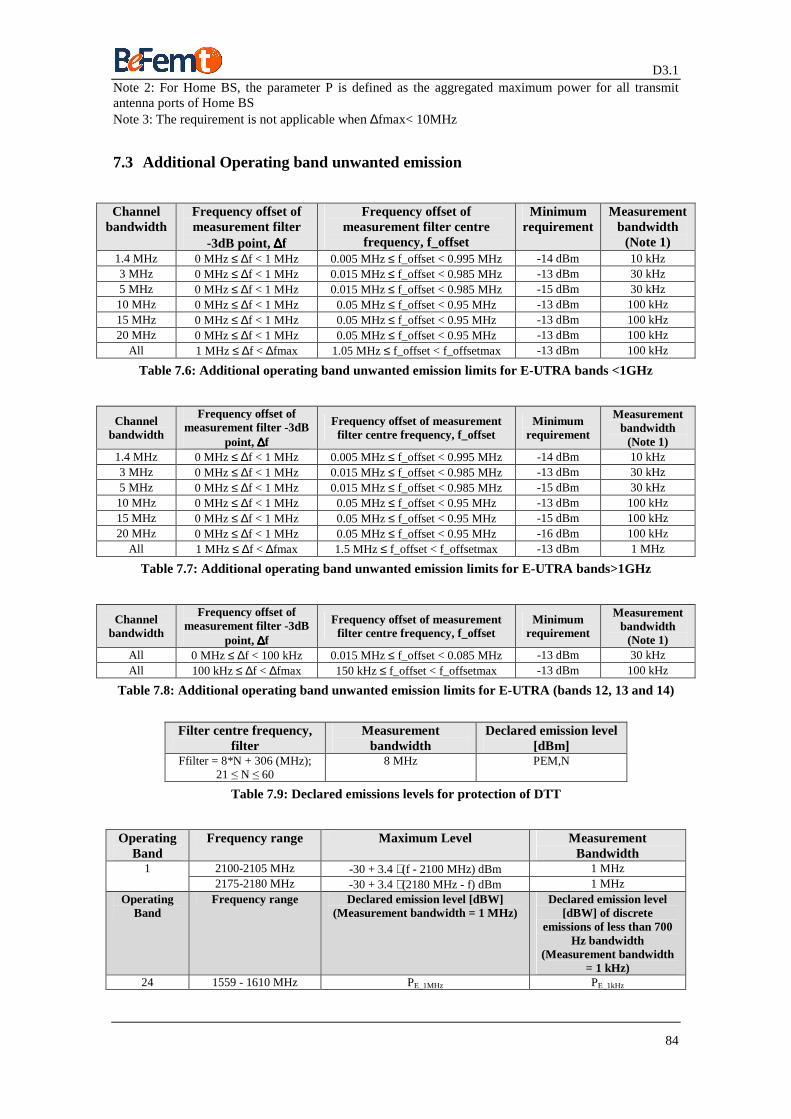
D3.1
84
Note 2: For Home BS, the parameter P is defined as the aggregated maximum power for all transmit antenna ports of Home BS Note 3: The requirement is not applicable when ∆fmax< 10MHz
7.3 Additional Operating band unwanted emission
Channel bandwidth
Frequency offset of measurement filter
-3dB point, ∆∆∆∆f
Frequency offset of measurement filter centre
frequency, f_offset
Minimum requirement
Measurement bandwidth
(Note 1) 1.4 MHz 0 MHz ≤ ∆f < 1 MHz 0.005 MHz ≤ f_offset < 0.995 MHz -14 dBm 10 kHz 3 MHz 0 MHz ≤ ∆f < 1 MHz 0.015 MHz ≤ f_offset < 0.985 MHz -13 dBm 30 kHz 5 MHz 0 MHz ≤ ∆f < 1 MHz 0.015 MHz ≤ f_offset < 0.985 MHz -15 dBm 30 kHz 10 MHz 0 MHz ≤ ∆f < 1 MHz 0.05 MHz ≤ f_offset < 0.95 MHz -13 dBm 100 kHz 15 MHz 0 MHz ≤ ∆f < 1 MHz 0.05 MHz ≤ f_offset < 0.95 MHz -13 dBm 100 kHz 20 MHz 0 MHz ≤ ∆f < 1 MHz 0.05 MHz ≤ f_offset < 0.95 MHz -13 dBm 100 kHz
All 1 MHz ≤ ∆f < ∆fmax 1.05 MHz ≤ f_offset < f_offsetmax -13 dBm 100 kHz
Table 7.6: Additional operating band unwanted emission limits for E-UTRA bands <1GHz
Channel bandwidth
Frequency offset of measurement filter -3dB
point, ∆∆∆∆f
Frequency offset of measurement filter centre frequency, f_offset
Minimum requirement
Measurement bandwidth
(Note 1) 1.4 MHz 0 MHz ≤ ∆f < 1 MHz 0.005 MHz ≤ f_offset < 0.995 MHz -14 dBm 10 kHz 3 MHz 0 MHz ≤ ∆f < 1 MHz 0.015 MHz ≤ f_offset < 0.985 MHz -13 dBm 30 kHz 5 MHz 0 MHz ≤ ∆f < 1 MHz 0.015 MHz ≤ f_offset < 0.985 MHz -15 dBm 30 kHz 10 MHz 0 MHz ≤ ∆f < 1 MHz 0.05 MHz ≤ f_offset < 0.95 MHz -13 dBm 100 kHz 15 MHz 0 MHz ≤ ∆f < 1 MHz 0.05 MHz ≤ f_offset < 0.95 MHz -15 dBm 100 kHz 20 MHz 0 MHz ≤ ∆f < 1 MHz 0.05 MHz ≤ f_offset < 0.95 MHz -16 dBm 100 kHz
All 1 MHz ≤ ∆f < ∆fmax 1.5 MHz ≤ f_offset < f_offsetmax -13 dBm 1 MHz
Table 7.7: Additional operating band unwanted emission limits for E-UTRA bands>1GHz
Channel bandwidth
Frequency offset of measurement filter -3dB
point, ∆∆∆∆f
Frequency offset of measurement filter centre frequency, f_offset
Minimum requirement
Measurement bandwidth
(Note 1) All 0 MHz ≤ ∆f < 100 kHz 0.015 MHz ≤ f_offset < 0.085 MHz -13 dBm 30 kHz All 100 kHz ≤ ∆f < ∆fmax 150 kHz ≤ f_offset < f_offsetmax -13 dBm 100 kHz
Table 7.8: Additional operating band unwanted emission limits for E-UTRA (bands 12, 13 and 14)
Filter centre frequency, filter
Measurement bandwidth
Declared emission level [dBm]
Ffilter = 8*N + 306 (MHz); 21 ≤ N ≤ 60
8 MHz PEM,N
Table 7.9: Declared emissions levels for protection of DTT
Operating Band
Frequency range Maximum Level Measurement Bandwidth
2100-2105 MHz -30 + 3.4 ⋅ (f - 2100 MHz) dBm 1 MHz 1 2175-2180 MHz -30 + 3.4 ⋅ (2180 MHz - f) dBm 1 MHz
Operating Band
Frequency range Declared emission level [dBW] (Measurement bandwidth = 1 MHz)
Declared emission level [dBW] of discrete
emissions of less than 700 Hz bandwidth
(Measurement bandwidth = 1 kHz)
24 1559 - 1610 MHz PE_1MHz PE_1kHz
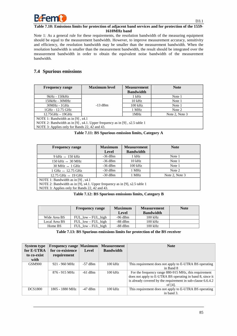
D3.1
85
Table 7.10: Emissions limits for protection of adjacent band services and for protection of the 1559-1610MHz band
Note 1: As a general rule for these requirements, the resolution bandwidth of the measuring equipment should be equal to the measurement bandwidth. However, to improve measurement accuracy, sensitivity and efficiency, the resolution bandwidth may be smaller than the measurement bandwidth. When the resolution bandwidth is smaller than the measurement bandwidth, the result should be integrated over the measurement bandwidth in order to obtain the equivalent noise bandwidth of the measurement bandwidth.
7.4 Spurious emissions
Frequency range Maximum level Measurement Bandwidth
Note
9kHz - 150kHz 1 kHz Note 1 150kHz - 30MHz 10 kHz Note 1 30MHz - 1GHz 100 kHz Note 1
1GHz - 12.75 GHz 1 MHz Note 2 12.75GHz – 19GHz
-13 dBm
1MHz Note 2, Note 3 NOTE 1: Bandwidth as in [9] , s4.1 NOTE 2: Bandwidth as in [9] , s4.1. Upper frequency as in [9] , s2.5 table 1 NOTE 3: Applies only for Bands 22, 42 and 43.
Table 7.11: BS Spurious emission limits, Category A
Frequency range Maximum Level
Measurement Bandwidth
Note
9 kHz ↔ 150 kHz -36 dBm 1 kHz Note 1 150 kHz ↔ 30 MHz -36 dBm 10 kHz Note 1 30 MHz ↔ 1 GHz -36 dBm 100 kHz Note 1
1 GHz ↔ 12.75 GHz -30 dBm 1 MHz Note 2 12.75 GHz ↔ 19 GHz -30 dBm 1 MHz Note 2, Note 3
NOTE 1: Bandwidth as in [9] , s4.1 NOTE 2: Bandwidth as in [9], s4.1. Upper frequency as in [9], s2.5 table 1 NOTE 3: Applies only for Bands 22, 42 and 43.
Table 7.12: BS Spurious emissions limits, Category B
Table 7.13: BS Spurious emissions limits for protection of the BS receiver
System type for E-UTRA to co-exist
with
Frequency range for co-existence
requirement
Maximum Level
Measurement Bandwidth
Note
921 - 960 MHz -57 dBm 100 kHz This requirement does not apply to E-UTRA BS operating in Band 8
GSM900
876 - 915 MHz -61 dBm 100 kHz For the frequency range 880-915 MHz, this requirement does not apply to E-UTRA BS operating in band 8, since it is already covered by the requirement in sub-clause 6.6.4.2
of [4]. DCS1800 1805 - 1880 MHz -47 dBm 100 kHz This requirement does not apply to E-UTRA BS operating
in band 3.
Frequency range Maximum Level
Measurement Bandwidth
Note
Wide Area BS FUL_low – FUL_high -96 dBm 100 kHz Local Area BS FUL_low – FUL_high -88 dBm 100 kHz
Home BS FUL_low – FUL_high -88 dBm 100 kHz
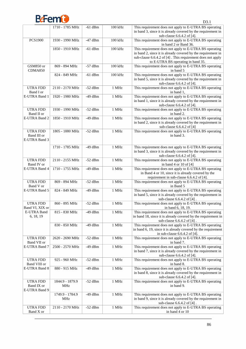
D3.1
86
1710 - 1785 MHz -61 dBm 100 kHz This requirement does not apply to E-UTRA BS operating in band 3, since it is already covered by the requirement in
sub-clause 6.6.4.2 of [4]. 1930 - 1990 MHz
-47 dBm 100 kHz This requirement does not apply to E-UTRA BS operating
in band 2 or Band 36. PCS1900
1850 - 1910 MHz
-61 dBm 100 kHz This requirement does not apply to E-UTRA BS operating in band 2, since it is already covered by the requirement in sub-clause 6.6.4.2 of [4] . This requirement does not apply
to E-UTRA BS operating in band 35. 869 - 894 MHz -57 dBm 100 kHz This requirement does not apply to E-UTRA BS operating
in band 5 GSM850 or CDMA850
824 - 849 MHz -61 dBm 100 kHz This requirement does not apply to E-UTRA BS operating in band 5, since it is already covered by the requirement in
sub-clause 6.6.4.2 of [4]. 2110 - 2170 MHz -52 dBm 1 MHz This requirement does not apply to E-UTRA BS operating
in band 1, UTRA FDD
Band I or E-UTRA Band 1 1920 - 1980 MHz
-49 dBm 1 MHz This requirement does not apply to E-UTRA BS operating
in band 1, since it is already covered by the requirement in sub-clause 6.6.4.2 of [4].
1930 - 1990 MHz
-52 dBm 1 MHz This requirement does not apply to E-UTRA BS operating in band 2.
UTRA FDD Band II or
E-UTRA Band 2 1850 - 1910 MHz
-49 dBm 1 MHz This requirement does not apply to E-UTRA BS operating in band 2, since it is already covered by the requirement in
sub-clause 6.6.4.2 of [4] 1805 - 1880 MHz
-52 dBm 1 MHz This requirement does not apply to E-UTRA BS operating
in band 3. UTRA FDD Band III or
E-UTRA Band 3
1710 - 1785 MHz -49 dBm 1 MHz This requirement does not apply to E-UTRA BS operating in band 3, since it is already covered by the requirement in
sub-clause 6.6.4.2 of [4]. 2110 - 2155 MHz -52 dBm 1 MHz This requirement does not apply to E-UTRA BS operating
in band 4 or 10 of [4] UTRA FDD Band IV or
E-UTRA Band 4 1710 - 1755 MHz -49 dBm 1 MHz This requirement does not apply to E-UTRA BS operating in Band 4 or 10, since it is already covered by the
requirement in sub-clause 6.6.4.2 of [4]. 869 - 894 MHz -52 dBm 1 MHz This requirement does not apply to E-UTRA BS operating
in Band 5 UTRA FDD Band V or
E-UTRA Band 5 824 - 849 MHz -49 dBm 1 MHz This requirement does not apply to E-UTRA BS operating in band 5, since it is already covered by the requirement in
sub-clause 6.6.4.2 of [4] . 860 - 895 MHz -52 dBm 1 MHz This requirement does not apply to E-UTRA BS operating
in band 6, 18, 19. 815 - 830 MHz -49 dBm 1 MHz This requirement does not apply to E-UTRA BS operating
in band 18, since it is already covered by the requirement in sub-clause 6.6.4.2 of [4] .
UTRA FDD Band VI, XIX or E-UTRA Band
6, 18, 19
830 - 850 MHz -49 dBm 1 MHz This requirement does not apply to E-UTRA BS operating in band 6, 19, since it is already covered by the requirement
in sub-clause 6.6.4.2 of [4]. 2620 - 2690 MHz -52 dBm 1 MHz This requirement does not apply to E-UTRA BS operating
in band 7. UTRA FDD Band VII or
E-UTRA Band 7 2500 - 2570 MHz -49 dBm 1 MHz This requirement does not apply to E-UTRA BS operating in band 7, since it is already covered by the requirement in
sub-clause 6.6.4.2 of [4]. 925 - 960 MHz -52 dBm 1 MHz This requirement does not apply to E-UTRA BS operating
in band 8. UTRA FDD Band VIII or
E-UTRA Band 8 880 - 915 MHz -49 dBm 1 MHz This requirement does not apply to E-UTRA BS operating in band 8, since it is already covered by the requirement in
sub-clause 6.6.4.2 of [4]. 1844.9 - 1879.9
MHz
-52 dBm 1 MHz This requirement does not apply to E-UTRA BS operating in band 9.
UTRA FDD Band IX or
E-UTRA Band 9 1749.9 - 1784.9
MHz -49 dBm 1 MHz This requirement does not apply to E-UTRA BS operating
in band 9, since it is already covered by the requirement in sub-clause 6.6.4.2 of [4] .
UTRA FDD Band X or
2110 - 2170 MHz -52 dBm 1 MHz This requirement does not apply to E-UTRA BS operating in band 4 or 10
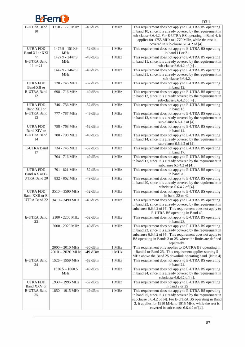
D3.1
87
E-UTRA Band 10
1710 - 1770 MHz -49 dBm 1 MHz This requirement does not apply to E-UTRA BS operating in band 10, since it is already covered by the requirement in sub-clause 6.6.4.2. For E-UTRA BS operating in Band 4, it
applies for 1755 MHz to 1770 MHz, while the rest is covered in sub-clause 6.6.4.2 of [4] .
1475.9 - 1510.9 MHz
-52 dBm 1 MHz This requirement does not apply to E-UTRA BS operating in band 11 or 21
1427.9 - 1447.9 MHz
-49 dBm 1 MHz This requirement does not apply to E-UTRA BS operating in band 11, since it is already covered by the requirement in
sub-clause 6.6.4.2 of [4] .
UTRA FDD Band XI or XXI
or E-UTRA Band
11 or 21 1447.9 - 1462.9
MHz -49 dBm 1 MHz This requirement does not apply to E-UTRA BS operating
in band 21, since it is already covered by the requirement in sub-clause 6.6.4.2.
728 - 746 MHz -52 dBm 1 MHz This requirement does not apply to E-UTRA BS operating in band 12.
UTRA FDD Band XII or
E-UTRA Band 12
698 - 716 MHz -49 dBm 1 MHz This requirement does not apply to E-UTRA BS operating in band 12, since it is already covered by the requirement in
sub-clause 6.6.4.2 of [4] . 746 - 756 MHz -52 dBm 1 MHz This requirement does not apply to E-UTRA BS operating
in band 13. UTRA FDD Band XIII or
E-UTRA Band 13
777 - 787 MHz -49 dBm 1 MHz This requirement does not apply to E-UTRA BS operating in band 13, since it is already covered by the requirement in
sub-clause 6.6.4.2 of [4]. 758 - 768 MHz -52 dBm 1 MHz This requirement does not apply to E-UTRA BS operating
in band 14. UTRA FDD Band XIV or
E-UTRA Band 14
788 - 798 MHz -49 dBm 1 MHz This requirement does not apply to E-UTRA BS operating in band 14, since it is already covered by the requirement in
sub-clause 6.6.4.2 of [4]. 734 - 746 MHz -52 dBm 1 MHz This requirement does not apply to E-UTRA BS operating
in band 17. E-UTRA Band
17 704 - 716 MHz -49 dBm 1 MHz This requirement does not apply to E-UTRA BS operating
in band 17, since it is already covered by the requirement in subclause 6.6.4.2 of [4] .
791 - 821 MHz -52 dBm 1 MHz This requirement does not apply to E-UTRA BS operating in band 20.
UTRA FDD Band XX or E-UTRA Band 20 832 - 862 MHz -49 dBm 1 MHz This requirement does not apply to E-UTRA BS operating
in band 20, since it is already covered by the requirement in subclause 6.6.4.2 of [4].
3510 – 3590 MHz -52 dBm 1 MHz This requirement does not apply to E-UTRA BS operating in band 22 or 42.
UTRA FDD Band XXII or E-UTRA Band 22 3410 – 3490 MHz -49 dBm 1 MHz This requirement does not apply to E-UTRA BS operating
in band 22, since it is already covered by the requirement in subclause 6.6.4.2 of [4]. This requirement does not apply to
E-UTRA BS operating in Band 42 2180 - 2200 MHz -52 dBm 1 MHz This requirement does not apply to E-UTRA BS operating
in band 23. 2000 - 2020 MHz -49 dBm 1 MHz This requirement does not apply to E-UTRA BS operating
in band 23, since it is already covered by the requirement in subclause 6.6.4.2 of [4]. This requirement does not apply to BS operating in Bands 2 or 25, where the limits are defined
separately. 2000 – 2010 MHz -30 dBm 1 MHz
E-UTRA Band 23
2010 – 2020 MHz -49 dBm 1 MHz This requirement only applies to E-UTRA BS operating in
Band 2 or Band 25. This requirement applies starting 5 MHz above the Band 25 downlink operating band. (Note 4)
1525 – 1559 MHz -52 dBm 1 MHz This requirement does not apply to E-UTRA BS operating in band 24.
E-UTRA Band 24
1626.5 – 1660.5 MHz
-49 dBm 1 MHz This requirement does not apply to E-UTRA BS operating in band 24, since it is already covered by the requirement in
subclause 6.6.4.2 of [4]. 1930 – 1995 MHz -52 dBm 1 MHz This requirement does not apply to E-UTRA BS operating
in band 2 or 25 UTRA FDD
Band XXV or E-UTRA Band
25 1850 – 1915 MHz -49 dBm 1 MHz This requirement does not apply to E-UTRA BS operating
in band 25, since it is already covered by the requirement in subclause 6.6.4.2 of [4]. For E-UTRA BS operating in Band 2, it applies for 1910 MHz to 1915 MHz, while the rest is
covered in sub-clause 6.6.4.2 of [4].
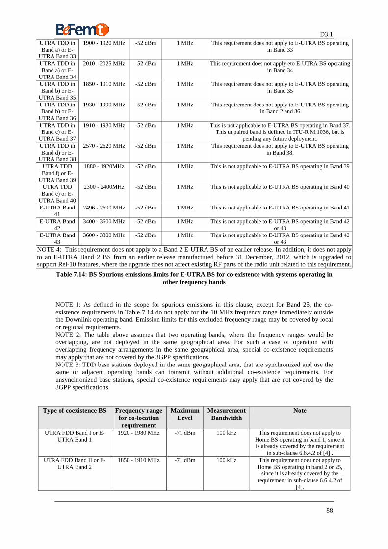
D3.1
88
UTRA TDD in Band a) or E-
UTRA Band 33
1900 - 1920 MHz
-52 dBm 1 MHz This requirement does not apply to E-UTRA BS operating in Band 33
UTRA TDD in Band a) or E-
UTRA Band 34
2010 - 2025 MHz -52 dBm 1 MHz This requirement does not apply eto E-UTRA BS operating in Band 34
UTRA TDD in Band b) or E-
UTRA Band 35
1850 - 1910 MHz
-52 dBm 1 MHz This requirement does not apply to E-UTRA BS operating in Band 35
UTRA TDD in Band b) or E-
UTRA Band 36
1930 - 1990 MHz -52 dBm 1 MHz This requirement does not apply to E-UTRA BS operating in Band 2 and 36
UTRA TDD in Band c) or E-
UTRA Band 37
1910 - 1930 MHz -52 dBm 1 MHz This is not applicable to E-UTRA BS operating in Band 37. This unpaired band is defined in ITU-R M.1036, but is
pending any future deployment. UTRA TDD in Band d) or E-
UTRA Band 38
2570 - 2620 MHz -52 dBm 1 MHz This requirement does not apply to E-UTRA BS operating in Band 38.
UTRA TDD Band f) or E-
UTRA Band 39
1880 - 1920MHz -52 dBm 1 MHz This is not applicable to E-UTRA BS operating in Band 39
UTRA TDD Band e) or E-
UTRA Band 40
2300 - 2400MHz -52 dBm 1 MHz This is not applicable to E-UTRA BS operating in Band 40
E-UTRA Band 41
2496 - 2690 MHz -52 dBm 1 MHz This is not applicable to E-UTRA BS operating in Band 41
E-UTRA Band 42
3400 - 3600 MHz -52 dBm 1 MHz This is not applicable to E-UTRA BS operating in Band 42 or 43
E-UTRA Band 43
3600 - 3800 MHz -52 dBm 1 MHz This is not applicable to E-UTRA BS operating in Band 42 or 43
NOTE 4: This requirement does not apply to a Band 2 E-UTRA BS of an earlier release. In addition, it does not apply to an E-UTRA Band 2 BS from an earlier release manufactured before 31 December, 2012, which is upgraded to support Rel-10 features, where the upgrade does not affect existing RF parts of the radio unit related to this requirement.
Table 7.14: BS Spurious emissions limits for E-UTRA BS for co-existence with systems operating in other frequency bands
NOTE 1: As defined in the scope for spurious emissions in this clause, except for Band 25, the co-existence requirements in Table 7.14 do not apply for the 10 MHz frequency range immediately outside the Downlink operating band. Emission limits for this excluded frequency range may be covered by local or regional requirements. NOTE 2: The table above assumes that two operating bands, where the frequency ranges would be overlapping, are not deployed in the same geographical area. For such a case of operation with overlapping frequency arrangements in the same geographical area, special co-existence requirements may apply that are not covered by the 3GPP specifications. NOTE 3: TDD base stations deployed in the same geographical area, that are synchronized and use the same or adjacent operating bands can transmit without additional co-existence requirements. For unsynchronized base stations, special co-existence requirements may apply that are not covered by the 3GPP specifications.
Type of coexistence BS Frequency range for co-location requirement
Maximum Level
Measurement Bandwidth
Note
UTRA FDD Band I or E-UTRA Band 1
1920 - 1980 MHz
-71 dBm 100 kHz This requirement does not apply to Home BS operating in band 1, since it is already covered by the requirement
in sub-clause 6.6.4.2 of [4] . UTRA FDD Band II or E-
UTRA Band 2 1850 - 1910 MHz
-71 dBm 100 kHz This requirement does not apply to
Home BS operating in band 2 or 25, since it is already covered by the
requirement in sub-clause 6.6.4.2 of [4].
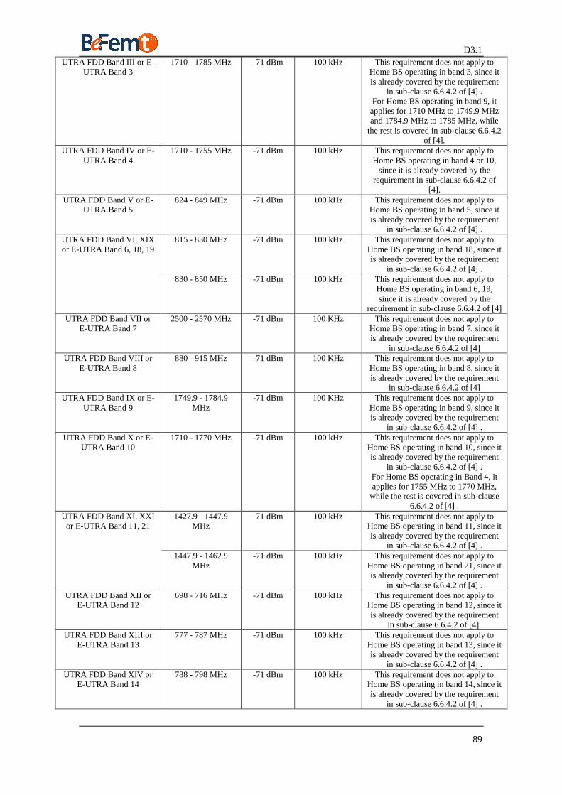
D3.1
89
UTRA FDD Band III or E-UTRA Band 3
1710 - 1785 MHz -71 dBm 100 kHz This requirement does not apply to Home BS operating in band 3, since it is already covered by the requirement
in sub-clause 6.6.4.2 of [4] . For Home BS operating in band 9, it applies for 1710 MHz to 1749.9 MHz and 1784.9 MHz to 1785 MHz, while
the rest is covered in sub-clause 6.6.4.2 of [4].
UTRA FDD Band IV or E-UTRA Band 4
1710 - 1755 MHz -71 dBm 100 kHz This requirement does not apply to Home BS operating in band 4 or 10,
since it is already covered by the requirement in sub-clause 6.6.4.2 of
[4]. UTRA FDD Band V or E-
UTRA Band 5 824 - 849 MHz -71 dBm 100 kHz This requirement does not apply to
Home BS operating in band 5, since it is already covered by the requirement
in sub-clause 6.6.4.2 of [4] . 815 - 830 MHz -71 dBm 100 kHz This requirement does not apply to
Home BS operating in band 18, since it is already covered by the requirement
in sub-clause 6.6.4.2 of [4] .
UTRA FDD Band VI, XIX or E-UTRA Band 6, 18, 19
830 - 850 MHz -71 dBm 100 kHz This requirement does not apply to Home BS operating in band 6, 19, since it is already covered by the
requirement in sub-clause 6.6.4.2 of [4] UTRA FDD Band VII or
E-UTRA Band 7 2500 - 2570 MHz -71 dBm 100 KHz This requirement does not apply to
Home BS operating in band 7, since it is already covered by the requirement
in sub-clause 6.6.4.2 of [4] UTRA FDD Band VIII or
E-UTRA Band 8 880 - 915 MHz -71 dBm 100 KHz This requirement does not apply to
Home BS operating in band 8, since it is already covered by the requirement
in sub-clause 6.6.4.2 of [4] UTRA FDD Band IX or E-
UTRA Band 9 1749.9 - 1784.9
MHz -71 dBm 100 KHz This requirement does not apply to
Home BS operating in band 9, since it is already covered by the requirement
in sub-clause 6.6.4.2 of [4] . UTRA FDD Band X or E-
UTRA Band 10 1710 - 1770 MHz -71 dBm 100 kHz This requirement does not apply to
Home BS operating in band 10, since it is already covered by the requirement
in sub-clause 6.6.4.2 of [4] . For Home BS operating in Band 4, it applies for 1755 MHz to 1770 MHz,
while the rest is covered in sub-clause 6.6.4.2 of [4] .
1427.9 - 1447.9 MHz
-71 dBm 100 kHz This requirement does not apply to Home BS operating in band 11, since it is already covered by the requirement
in sub-clause 6.6.4.2 of [4] .
UTRA FDD Band XI, XXI or E-UTRA Band 11, 21
1447.9 - 1462.9 MHz
-71 dBm 100 kHz This requirement does not apply to Home BS operating in band 21, since it is already covered by the requirement
in sub-clause 6.6.4.2 of [4] . UTRA FDD Band XII or
E-UTRA Band 12 698 - 716 MHz -71 dBm 100 kHz This requirement does not apply to
Home BS operating in band 12, since it is already covered by the requirement
in sub-clause 6.6.4.2 of [4]. UTRA FDD Band XIII or
E-UTRA Band 13 777 - 787 MHz -71 dBm 100 kHz This requirement does not apply to
Home BS operating in band 13, since it is already covered by the requirement
in sub-clause 6.6.4.2 of [4] . UTRA FDD Band XIV or
E-UTRA Band 14 788 - 798 MHz -71 dBm 100 kHz This requirement does not apply to
Home BS operating in band 14, since it is already covered by the requirement
in sub-clause 6.6.4.2 of [4] .
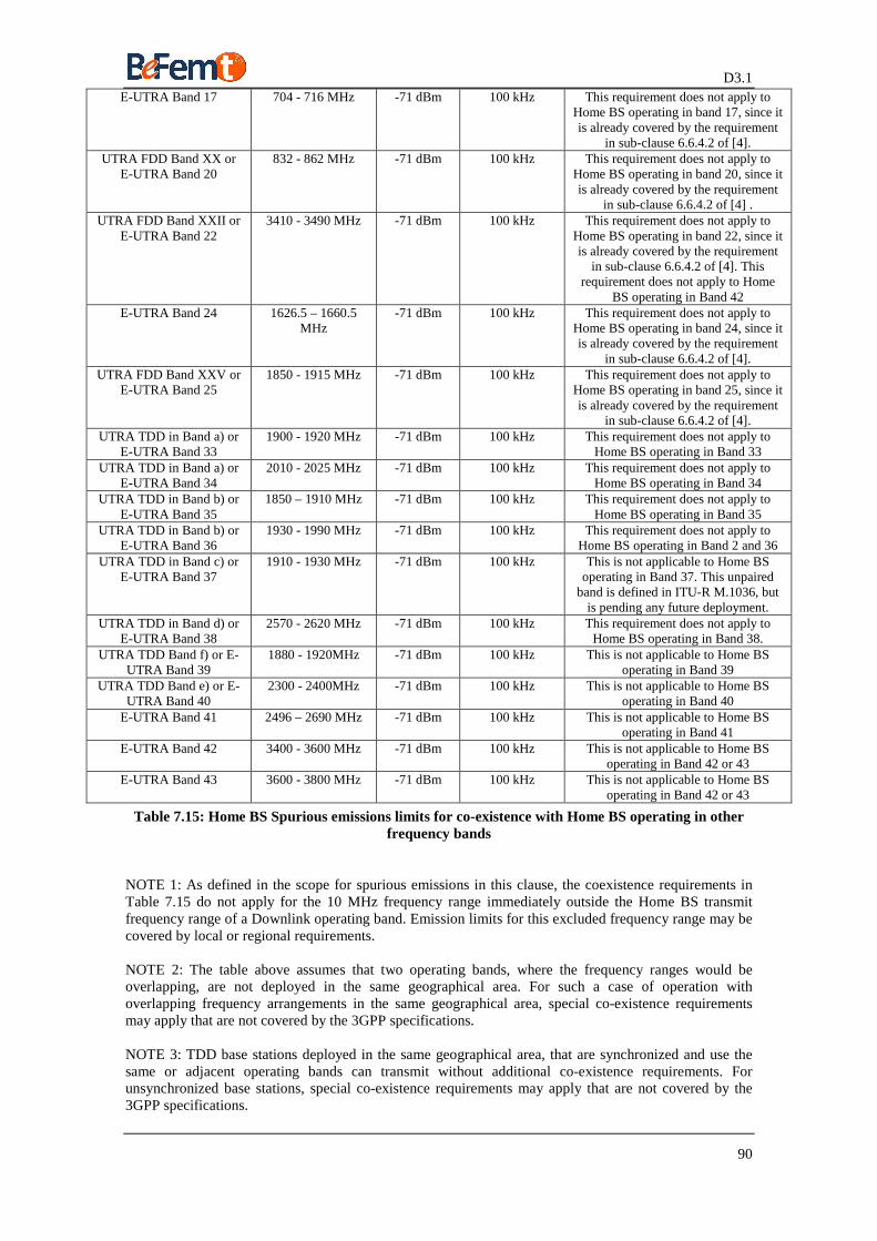
D3.1
90
E-UTRA Band 17 704 - 716 MHz -71 dBm 100 kHz This requirement does not apply to Home BS operating in band 17, since it is already covered by the requirement
in sub-clause 6.6.4.2 of [4]. UTRA FDD Band XX or
E-UTRA Band 20 832 - 862 MHz -71 dBm 100 kHz This requirement does not apply to
Home BS operating in band 20, since it is already covered by the requirement
in sub-clause 6.6.4.2 of [4] . UTRA FDD Band XXII or
E-UTRA Band 22 3410 - 3490 MHz -71 dBm 100 kHz This requirement does not apply to
Home BS operating in band 22, since it is already covered by the requirement
in sub-clause 6.6.4.2 of [4]. This requirement does not apply to Home
BS operating in Band 42 E-UTRA Band 24 1626.5 – 1660.5
MHz -71 dBm 100 kHz This requirement does not apply to
Home BS operating in band 24, since it is already covered by the requirement
in sub-clause 6.6.4.2 of [4]. UTRA FDD Band XXV or
E-UTRA Band 25 1850 - 1915 MHz -71 dBm 100 kHz This requirement does not apply to
Home BS operating in band 25, since it is already covered by the requirement
in sub-clause 6.6.4.2 of [4]. UTRA TDD in Band a) or
E-UTRA Band 33 1900 - 1920 MHz
-71 dBm 100 kHz This requirement does not apply to
Home BS operating in Band 33 UTRA TDD in Band a) or
E-UTRA Band 34 2010 - 2025 MHz -71 dBm 100 kHz This requirement does not apply to
Home BS operating in Band 34 UTRA TDD in Band b) or
E-UTRA Band 35 1850 – 1910 MHz
-71 dBm 100 kHz This requirement does not apply to
Home BS operating in Band 35 UTRA TDD in Band b) or
E-UTRA Band 36 1930 - 1990 MHz -71 dBm 100 kHz This requirement does not apply to
Home BS operating in Band 2 and 36 UTRA TDD in Band c) or
E-UTRA Band 37 1910 - 1930 MHz -71 dBm 100 kHz This is not applicable to Home BS
operating in Band 37. This unpaired band is defined in ITU-R M.1036, but
is pending any future deployment. UTRA TDD in Band d) or
E-UTRA Band 38 2570 - 2620 MHz -71 dBm 100 kHz This requirement does not apply to
Home BS operating in Band 38. UTRA TDD Band f) or E-
UTRA Band 39 1880 - 1920MHz -71 dBm 100 kHz This is not applicable to Home BS
operating in Band 39 UTRA TDD Band e) or E-
UTRA Band 40 2300 - 2400MHz -71 dBm 100 kHz This is not applicable to Home BS
operating in Band 40 E-UTRA Band 41 2496 – 2690 MHz -71 dBm 100 kHz This is not applicable to Home BS
operating in Band 41 E-UTRA Band 42 3400 - 3600 MHz -71 dBm 100 kHz This is not applicable to Home BS
operating in Band 42 or 43 E-UTRA Band 43 3600 - 3800 MHz -71 dBm 100 kHz This is not applicable to Home BS
operating in Band 42 or 43
Table 7.15: Home BS Spurious emissions limits for co-existence with Home BS operating in other frequency bands
NOTE 1: As defined in the scope for spurious emissions in this clause, the coexistence requirements in Table 7.15 do not apply for the 10 MHz frequency range immediately outside the Home BS transmit frequency range of a Downlink operating band. Emission limits for this excluded frequency range may be covered by local or regional requirements. NOTE 2: The table above assumes that two operating bands, where the frequency ranges would be overlapping, are not deployed in the same geographical area. For such a case of operation with overlapping frequency arrangements in the same geographical area, special co-existence requirements may apply that are not covered by the 3GPP specifications. NOTE 3: TDD base stations deployed in the same geographical area, that are synchronized and use the same or adjacent operating bands can transmit without additional co-existence requirements. For unsynchronized base stations, special co-existence requirements may apply that are not covered by the 3GPP specifications.
D3.1
91
Frequency range Maximum Level
Measurement Bandwidth
Note
1884.5 - 1919.6 MHz -41 dBm 300 kHz Applicable when co-existence with PHS system operating in. 1884.5-1919.6MHz.
1884.5 - 1915.7 MHz -41 dBm 300 kHz Applicable when co-existence with PHS system operating in 1884.5-1915.7MHz
Table 7.16: E-UTRA BS Spurious emissions limits for BS for co-existence with PHS
Operating Band Frequency range Maximum Level
Measurement Bandwidth
Note
13 763 - 775 MHz -46 dBm 6.25 kHz 13 793 - 805 MHz -46 dBm 6.25 kHz 14 769 - 775 MHz -46 dBm 6.25 kHz 14 799 - 805 MHz -46 dBm 6.25 kHz
Table 7.17: BS Spurious emissions limits for protection of public safety operations
7.5 Transmitter intermodulation
Parameter Value Wanted signal E-UTRA single carrier, or multi-carrier, or multiple intra-band
contiguously aggregated carriers Interfering signal type E-UTRA signal of channel bandwidth 5 MHz Interfering signal level Mean power level 30 dB below the mean power of the wanted signal
Interfering signal centre frequency offset from the lower (higher) edge of the wanted signal
± 2.5 MHz ± 7.5 MHz ± 12.5 MHz
NOTE1: Interfering signal positions that are partially or completely outside of the Downlink operating band of the base station are excluded from the requirement, unless the interfering signal positions fall within the frequency range of adjacent Downlink operating bands in the same geographical area. In case that none of the interfering signal positions fall completely within the frequency range of the Downlink operating band, TS 36.141 provides further guidance regarding appropriate test requirements. NOTE2: NOTE 1 is not applied in Band 1, 3, 9, 11, 18, 19, 21 and 34 in certain regions.
Table 7.18: Interfering and wanted signals for the Transmitter intermodulation requirement
7.6 Reference sensitivity levels
E-UTRA
channel bandwidth [MHz]
Reference measurement channel
Reference sensitivity power level, PREFSENS
[dBm] 1.4 FRC A1-1 in Table 7.20* -98.8 3 FRC A1-2 in Table 7.20 -95.0 5 FRC A1-3 in Table 7.20* -93.5 10 FRC A1-3 in Table 7.20 -93.5 15 FRC A1-3 in Table 7.20* -93.5 20 FRC A1-3 in Table 7.20* -93.5
Note*: PREFSENS is the power level of a single instance of the reference measurement channel. This requirement shall be met for each consecutive application of a single instance of FRC A1-3 mapped to disjoint frequency ranges with a width of 25 resource blocks each
Table 7.19: Home BS reference sensitivity levels
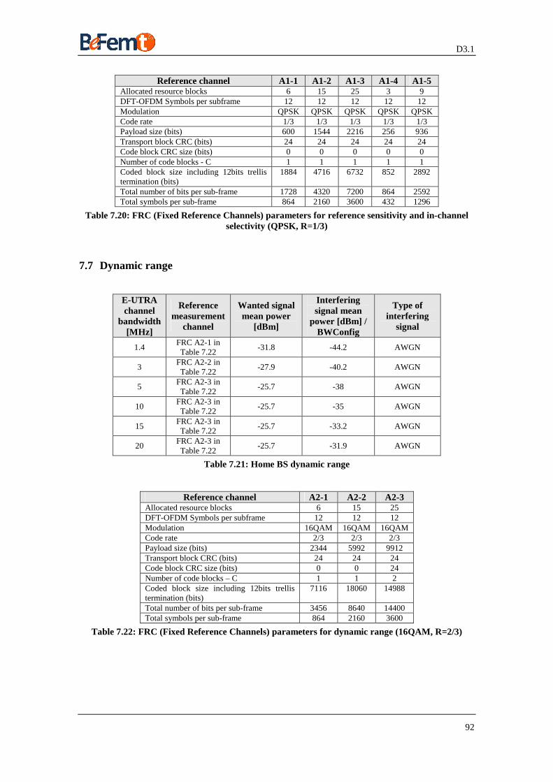
D3.1
92
Reference channel A1-1 A1-2 A1-3 A1-4 A1-5 Allocated resource blocks 6 15 25 3 9 DFT-OFDM Symbols per subframe 12 12 12 12 12 Modulation QPSK QPSK QPSK QPSK QPSK Code rate 1/3 1/3 1/3 1/3 1/3 Payload size (bits) 600 1544 2216 256 936 Transport block CRC (bits) 24 24 24 24 24 Code block CRC size (bits) 0 0 0 0 0 Number of code blocks - C 1 1 1 1 1 Coded block size including 12bits trellis termination (bits)
1884 4716 6732 852 2892
Total number of bits per sub-frame 1728 4320 7200 864 2592 Total symbols per sub-frame 864 2160 3600 432 1296
Table 7.20: FRC (Fixed Reference Channels) parameters for reference sensitivity and in-channel selectivity (QPSK, R=1/3)
7.7 Dynamic range
E-UTRA channel
bandwidth [MHz]
Reference measurement
channel
Wanted signal mean power
[dBm]
Interfering signal mean
power [dBm] / BWConfig
Type of interfering
signal
1.4 FRC A2-1 in Table 7.22
-31.8 -44.2 AWGN
3 FRC A2-2 in Table 7.22
-27.9 -40.2 AWGN
5 FRC A2-3 in Table 7.22
-25.7 -38 AWGN
10 FRC A2-3 in Table 7.22
-25.7 -35 AWGN
15 FRC A2-3 in Table 7.22
-25.7 -33.2 AWGN
20 FRC A2-3 in Table 7.22
-25.7 -31.9 AWGN
Table 7.21: Home BS dynamic range
Reference channel A2-1 A2-2 A2-3 Allocated resource blocks 6 15 25 DFT-OFDM Symbols per subframe 12 12 12 Modulation 16QAM 16QAM 16QAM Code rate 2/3 2/3 2/3 Payload size (bits) 2344 5992 9912 Transport block CRC (bits) 24 24 24 Code block CRC size (bits) 0 0 24 Number of code blocks – C 1 1 2 Coded block size including 12bits trellis termination (bits)
7116 18060 14988
Total number of bits per sub-frame 3456 8640 14400 Total symbols per sub-frame 864 2160 3600
Table 7.22: FRC (Fixed Reference Channels) parameters for dynamic range (16QAM, R=2/3)
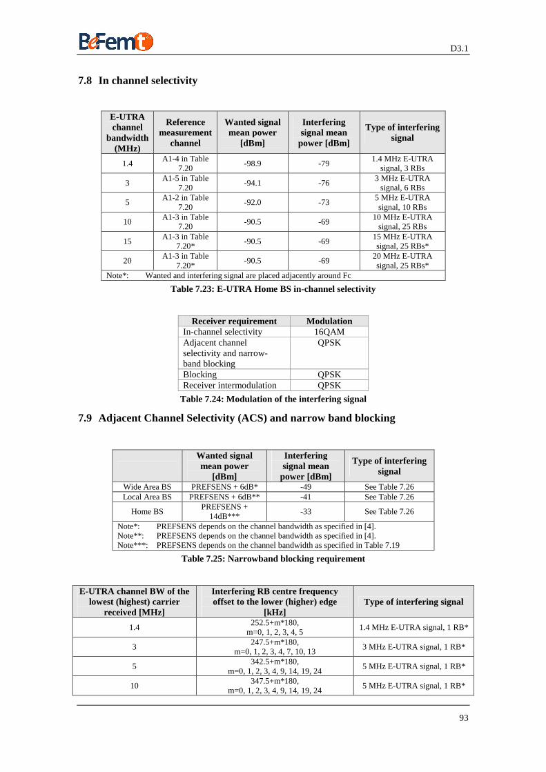
D3.1
93
7.8 In channel selectivity
E-UTRA channel
bandwidth (MHz)
Reference measurement
channel
Wanted signal mean power
[dBm]
Interfering signal mean power [dBm]
Type of interfering signal
1.4 A1-4 in Table
7.20 -98.9 -79
1.4 MHz E-UTRA signal, 3 RBs
3 A1-5 in Table
7.20 -94.1 -76
3 MHz E-UTRA signal, 6 RBs
5 A1-2 in Table
7.20 -92.0 -73
5 MHz E-UTRA signal, 10 RBs
10 A1-3 in Table
7.20 -90.5 -69
10 MHz E-UTRA signal, 25 RBs
15 A1-3 in Table
7.20* -90.5 -69
15 MHz E-UTRA signal, 25 RBs*
20 A1-3 in Table
7.20* -90.5 -69
20 MHz E-UTRA signal, 25 RBs*
Note*: Wanted and interfering signal are placed adjacently around Fc
Table 7.23: E-UTRA Home BS in-channel selectivity
Receiver requirement Modulation In-channel selectivity 16QAM Adjacent channel selectivity and narrow-band blocking
QPSK
Blocking QPSK Receiver intermodulation QPSK
Table 7.24: Modulation of the interfering signal
7.9 Adjacent Channel Selectivity (ACS) and narrow band blocking
Wanted signal mean power
[dBm]
Interfering signal mean power [dBm]
Type of interfering signal
Wide Area BS PREFSENS + 6dB* -49 See Table 7.26 Local Area BS PREFSENS + 6dB** -41 See Table 7.26
Home BS PREFSENS +
14dB*** -33 See Table 7.26
Note*: PREFSENS depends on the channel bandwidth as specified in [4]. Note**: PREFSENS depends on the channel bandwidth as specified in [4]. Note***: PREFSENS depends on the channel bandwidth as specified in Table 7.19
Table 7.25: Narrowband blocking requirement
E-UTRA channel BW of the lowest (highest) carrier
received [MHz]
Interfering RB centre frequency offset to the lower (higher) edge
[kHz] Type of interfering signal
1.4 252.5+m*180,
m=0, 1, 2, 3, 4, 5 1.4 MHz E-UTRA signal, 1 RB*
3 247.5+m*180,
m=0, 1, 2, 3, 4, 7, 10, 13 3 MHz E-UTRA signal, 1 RB*
5 342.5+m*180,
m=0, 1, 2, 3, 4, 9, 14, 19, 24 5 MHz E-UTRA signal, 1 RB*
10 347.5+m*180,
m=0, 1, 2, 3, 4, 9, 14, 19, 24 5 MHz E-UTRA signal, 1 RB*
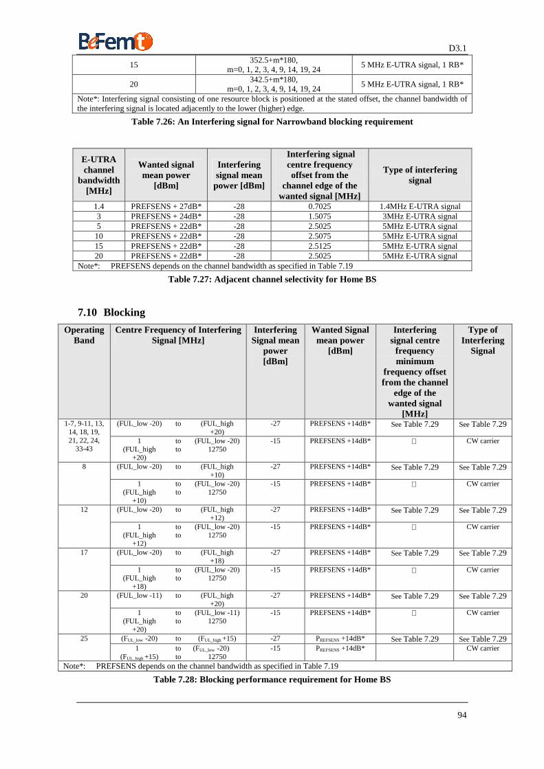
D3.1
94
15 352.5+m*180,
m=0, 1, 2, 3, 4, 9, 14, 19, 24 5 MHz E-UTRA signal, 1 RB*
20 342.5+m*180,
m=0, 1, 2, 3, 4, 9, 14, 19, 24 5 MHz E-UTRA signal, 1 RB*
Note*: Interfering signal consisting of one resource block is positioned at the stated offset, the channel bandwidth of the interfering signal is located adjacently to the lower (higher) edge.
Table 7.26: An Interfering signal for Narrowband blocking requirement
E-UTRA channel
bandwidth [MHz]
Wanted signal mean power
[dBm]
Interfering signal mean power [dBm]
Interfering signal centre frequency offset from the
channel edge of the wanted signal [MHz]
Type of interfering signal
1.4 PREFSENS + 27dB* -28 0.7025 1.4MHz E-UTRA signal 3 PREFSENS + 24dB* -28 1.5075 3MHz E-UTRA signal 5 PREFSENS + 22dB* -28 2.5025 5MHz E-UTRA signal 10 PREFSENS + 22dB* -28 2.5075 5MHz E-UTRA signal 15 PREFSENS + 22dB* -28 2.5125 5MHz E-UTRA signal 20 PREFSENS + 22dB* -28 2.5025 5MHz E-UTRA signal
Note*: PREFSENS depends on the channel bandwidth as specified in Table 7.19
Table 7.27: Adjacent channel selectivity for Home BS
7.10 Blocking
Operating Band
Centre Frequency of Interfering Signal [MHz]
Interfering Signal mean
power [dBm]
Wanted Signal mean power
[dBm]
Interfering signal centre
frequency minimum
frequency offset from the channel
edge of the wanted signal
[MHz]
Type of Interfering
Signal
(FUL_low -20) to (FUL_high +20)
-27 PREFSENS +14dB* See Table 7.29 See Table 7.29 1-7, 9-11, 13, 14, 18, 19, 21, 22, 24,
33-43 1
(FUL_high +20)
to to
(FUL_low -20) 12750
-15 PREFSENS +14dB* CW carrier
(FUL_low -20) to (FUL_high +10)
-27 PREFSENS +14dB* See Table 7.29 See Table 7.29 8
1 (FUL_high
+10)
to to
(FUL_low -20) 12750
-15 PREFSENS +14dB* CW carrier
(FUL_low -20) to (FUL_high +12)
-27 PREFSENS +14dB* See Table 7.29 See Table 7.29 12
1 (FUL_high
+12)
to to
(FUL_low -20) 12750
-15 PREFSENS +14dB* CW carrier
(FUL_low -20) to (FUL_high +18)
-27 PREFSENS +14dB* See Table 7.29 See Table 7.29 17
1 (FUL_high
+18)
to to
(FUL_low -20) 12750
-15 PREFSENS +14dB* CW carrier
(FUL_low -11) to (FUL_high +20)
-27 PREFSENS +14dB* See Table 7.29 See Table 7.29 20
1 (FUL_high
+20)
to to
(FUL_low -11) 12750
-15 PREFSENS +14dB* CW carrier
(FUL_low -20) to (FUL_high +15) -27 PREFSENS +14dB* See Table 7.29 See Table 7.29 25 1
(FUL_high +15) to to
(FUL_low -20) 12750
-15 PREFSENS +14dB* CW carrier
Note*: PREFSENS depends on the channel bandwidth as specified in Table 7.19
Table 7.28: Blocking performance requirement for Home BS
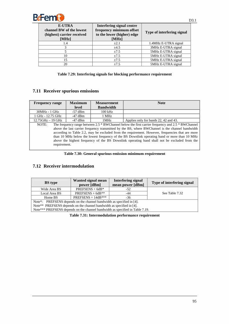
D3.1
95
E-UTRA channel BW of the lowest (highest) carrier received
[MHz]
Interfering signal centre frequency minimum offset to the lower (higher) edge
[MHz]
Type of interfering signal
1.4 ±2.1 1.4MHz E-UTRA signal 3 ±4.5 3MHz E-UTRA signal 5 ±7.5 5MHz E-UTRA signal 10 ±7.5 5MHz E-UTRA signal 15 ±7.5 5MHz E-UTRA signal 20 ±7.5 5MHz E-UTRA signal
Table 7.29: Interfering signals for blocking performance requirement
7.11 Receiver spurious emissions
Frequency range Maximum
level Measurement
Bandwidth Note
30MHz - 1 GHz -57 dBm 100 kHz 1 GHz - 12.75 GHz -47 dBm 1 MHz 12.75GHz – 19 GHz -47 dBm 1MHz Applies only for bands 22, 42 and 43.
NOTE: The frequency range between 2.5 * BWChannel below the first carrier frequency and 2.5 * BWChannel above the last carrier frequency transmitted by the BS, where BWChannel is the channel bandwidth according to Table 2.2, may be excluded from the requirement. However, frequencies that are more than 10 MHz below the lowest frequency of the BS Downlink operating band or more than 10 MHz above the highest frequency of the BS Downlink operating band shall not be excluded from the requirement.
Table 7.30: General spurious emission minimum requirement
7.12 Receiver intermodulation
BS type Wanted signal mean
power [dBm] Interfering signal
mean power [dBm] Type of interfering signal
Wide Area BS PREFSENS + 6dB* -52 Local Area BS PREFSENS + 6dB** -44
Home BS PREFSENS + 14dB*** -36 See Table 7.32
Note*: PREFSENS depends on the channel bandwidth as specified in [4]. Note** PREFSENS depends on the channel bandwidth as specified in [4]. Note*** PREFSENS depends on the channel bandwidth as specified in Table 7.19.
Table 7.31: Intermodulation performance requirement
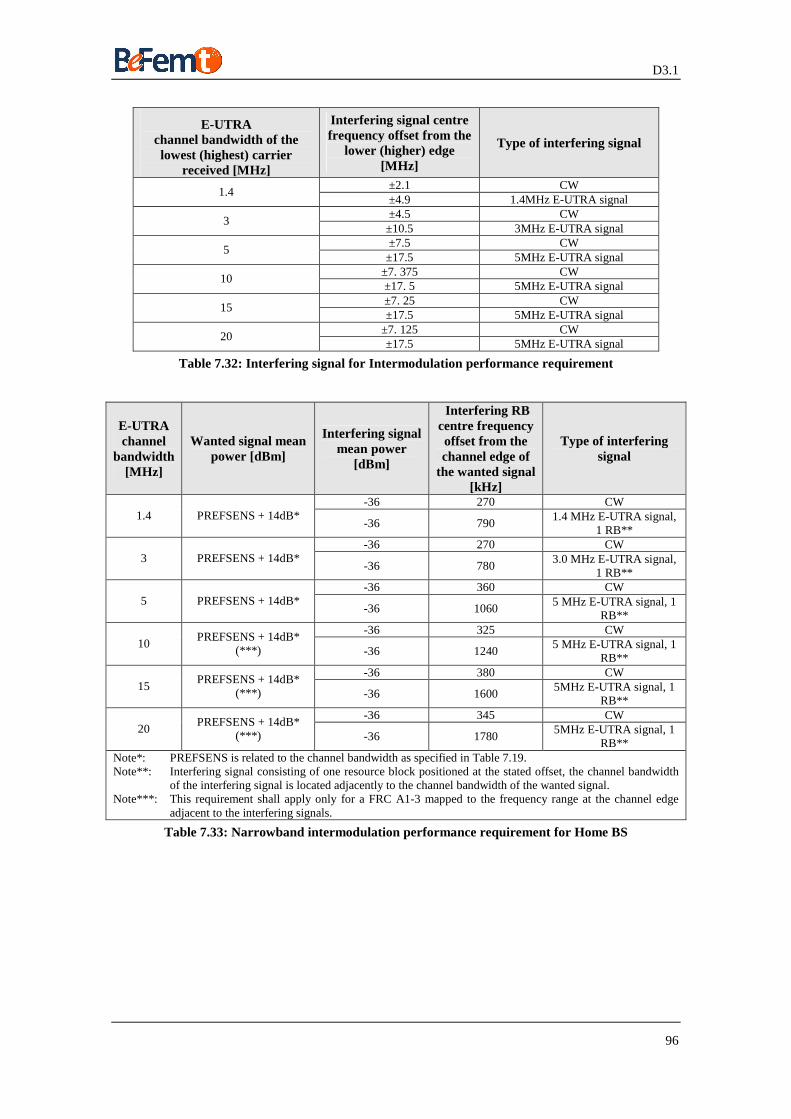
D3.1
96
E-UTRA channel bandwidth of the lowest (highest) carrier
received [MHz]
Interfering signal centre frequency offset from the
lower (higher) edge [MHz]
Type of interfering signal
±2.1 CW 1.4
±4.9 1.4MHz E-UTRA signal ±4.5 CW
3 ±10.5 3MHz E-UTRA signal ±7.5 CW
5 ±17.5 5MHz E-UTRA signal
±7. 375 CW 10
±17. 5 5MHz E-UTRA signal ±7. 25 CW
15 ±17.5 5MHz E-UTRA signal
±7. 125 CW 20
±17.5 5MHz E-UTRA signal
Table 7.32: Interfering signal for Intermodulation performance requirement
E-UTRA channel
bandwidth [MHz]
Wanted signal mean power [dBm]
Interfering signal mean power
[dBm]
Interfering RB centre frequency offset from the channel edge of
the wanted signal [kHz]
Type of interfering signal
-36 270 CW 1.4 PREFSENS + 14dB*
-36 790 1.4 MHz E-UTRA signal,
1 RB** -36 270 CW
3 PREFSENS + 14dB* -36 780
3.0 MHz E-UTRA signal, 1 RB**
-36 360 CW 5 PREFSENS + 14dB*
-36 1060 5 MHz E-UTRA signal, 1
RB** -36 325 CW
10 PREFSENS + 14dB*
(***) -36 1240 5 MHz E-UTRA signal, 1
RB** -36 380 CW
15 PREFSENS + 14dB*
(***) -36 1600 5MHz E-UTRA signal, 1
RB** -36 345 CW
20 PREFSENS + 14dB*
(***) -36 1780 5MHz E-UTRA signal, 1
RB** Note*: PREFSENS is related to the channel bandwidth as specified in Table 7.19. Note**: Interfering signal consisting of one resource block positioned at the stated offset, the channel bandwidth
of the interfering signal is located adjacently to the channel bandwidth of the wanted signal. Note***: This requirement shall apply only for a FRC A1-3 mapped to the frequency range at the channel edge
adjacent to the interfering signals.
Table 7.33: Narrowband intermodulation performance requirement for Home BS
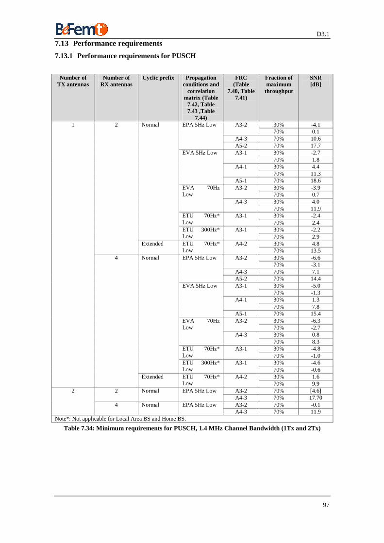
D3.1
97
7.13 Performance requirements
7.13.1 Performance requirements for PUSCH
Table 7.34: Minimum requirements for PUSCH, 1.4 MHz Channel Bandwidth (1Tx and 2Tx)
Number of TX antennas
Number of RX antennas
Cyclic prefix Propagation conditions and
correlation matrix (Table
7.42, Table 7.43 ,Table
7.44)
FRC (Table
7.40, Table 7.41)
Fraction of maximum
throughput
SNR [dB]
30% -4.1 A3-2 70% 0.1
A4-3 70% 10.6
EPA 5Hz Low
A5-2 70% 17.7 30% -2.7 A3-1 70% 1.8 30% 4.4 A4-1 70% 11.3
EVA 5Hz Low
A5-1 70% 18.6 30% -3.9 A3-2 70% 0.7 30% 4.0
EVA 70Hz Low
A4-3 70% 11.9 30% -2.4 ETU 70Hz*
Low A3-1
70% 2.4 30% -2.2
Normal
ETU 300Hz* Low
A3-1 70% 2.9 30% 4.8
2
Extended ETU 70Hz* Low
A4-2 70% 13.5 30% -6.6 A3-2 70% -3.1
A4-3 70% 7.1
EPA 5Hz Low
A5-2 70% 14.4 30% -5.0 A3-1 70% -1.3 30% 1.3 A4-1 70% 7.8
EVA 5Hz Low
A5-1 70% 15.4 30% -6.3 A3-2 70% -2.7 30% 0.8
EVA 70Hz Low
A4-3 70% 8.3 30% -4.8 ETU 70Hz*
Low A3-1
70% -1.0 30% -4.6
Normal
ETU 300Hz* Low
A3-1 70% -0.6 30% 1.6
1
4
Extended ETU 70Hz* Low
A4-2 70% 9.9
A3-2 70% [4.6] 2 Normal EPA 5Hz Low A4-3 70% 17.70 A3-2 70% -0.1
2
4 Normal EPA 5Hz Low A4-3 70% 11.9
Note*: Not applicable for Local Area BS and Home BS.
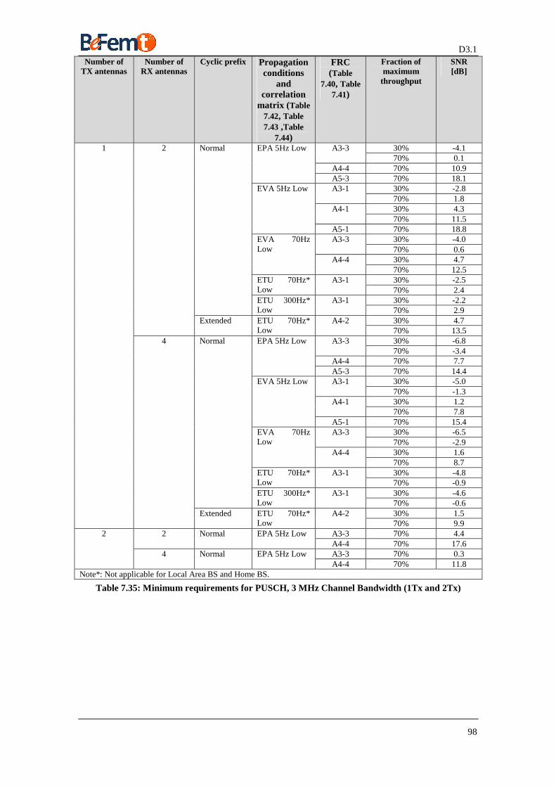
D3.1
98
Number of TX antennas
Number of RX antennas
Cyclic prefix Propagation conditions
and correlation
matrix ( Table 7.42, Table 7.43 ,Table
7.44)
FRC (Table
7.40, Table 7.41)
Fraction of maximum
throughput
SNR [dB]
30% -4.1 A3-3 70% 0.1
A4-4 70% 10.9
EPA 5Hz Low
A5-3 70% 18.1 30% -2.8 A3-1 70% 1.8 30% 4.3 A4-1 70% 11.5
EVA 5Hz Low
A5-1 70% 18.8 30% -4.0 A3-3 70% 0.6 30% 4.7
EVA 70Hz Low
A4-4 70% 12.5 30% -2.5 ETU 70Hz*
Low A3-1
70% 2.4 30% -2.2
Normal
ETU 300Hz* Low
A3-1 70% 2.9 30% 4.7
2
Extended ETU 70Hz* Low
A4-2 70% 13.5 30% -6.8 A3-3 70% -3.4
A4-4 70% 7.7
EPA 5Hz Low
A5-3 70% 14.4 30% -5.0 A3-1 70% -1.3 30% 1.2 A4-1 70% 7.8
EVA 5Hz Low
A5-1 70% 15.4 30% -6.5 A3-3 70% -2.9 30% 1.6
EVA 70Hz Low
A4-4 70% 8.7 30% -4.8 ETU 70Hz*
Low A3-1
70% -0.9 30% -4.6
Normal
ETU 300Hz* Low
A3-1 70% -0.6 30% 1.5
1
4
Extended ETU 70Hz* Low
A4-2 70% 9.9
A3-3 70% 4.4 2 Normal EPA 5Hz Low A4-4 70% 17.6 A3-3 70% 0.3
2
4 Normal EPA 5Hz Low A4-4 70% 11.8
Note*: Not applicable for Local Area BS and Home BS.
Table 7.35: Minimum requirements for PUSCH, 3 MHz Channel Bandwidth (1Tx and 2Tx)
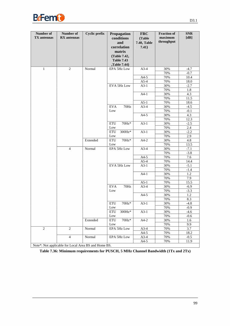
D3.1
99
Number of TX antennas
Number of RX antennas
Cyclic prefix Propagation conditions
and correlation
matrix (Table 7.42, Table 7.43
,Table 7.44)
FRC (Table
7.40, Table 7.41)
Fraction of maximum
throughput
SNR [dB]
30% -4.7 A3-4 70% -0.7
A4-5 70% 10.4
EPA 5Hz Low
A5-4 70% 18.0 30% -2.7 A3-1 70% 1.8 30% 4.3 A4-1 70% 11.5
EVA 5Hz Low
A5-1 70% 18.6 30% -4.5 A3-4 70% -0.1 30% 4.3
EVA 70Hz Low
A4-5 70% 12.3 30% -2.5 ETU 70Hz*
Low A3-1
70% 2.4 30% -2.2
Normal
ETU 300Hz* Low
A3-1 70% 2.9 30% 4.8
2
Extended ETU 70Hz* Low
A4-2 70% 13.5 30% -7.1 A3-4 70% -3.8
A4-5 70% 7.6
EPA 5Hz Low
A5-4 70% 14.4 30% -5.1 A3-1 70% -1.4 30% 1.2 A4-1 70% 7.9
EVA 5Hz Low
A5-1 70% 15.5 30% -6.9 A3-4 70% -3.3 30% 1.2
EVA 70Hz Low
A4-5 70% 8.3 30% -4.8 ETU 70Hz*
Low A3-1
70% -0.9 30% -4.6
Normal
ETU 300Hz* Low
A3-1 70% -0.6 30% 1.6
1
4
Extended ETU 70Hz* Low
A4-2 70% 9.9
A3-4 70% 3.7 2 Normal EPA 5Hz Low A4-5 70% 18.2 A3-4 70% -0.5
2
4 Normal EPA 5Hz Low A4-5 70% 11.9
Note*: Not applicable for Local Area BS and Home BS.
Table 7.36: Minimum requirements for PUSCH, 5 MHz Channel Bandwidth (1Tx and 2Tx)
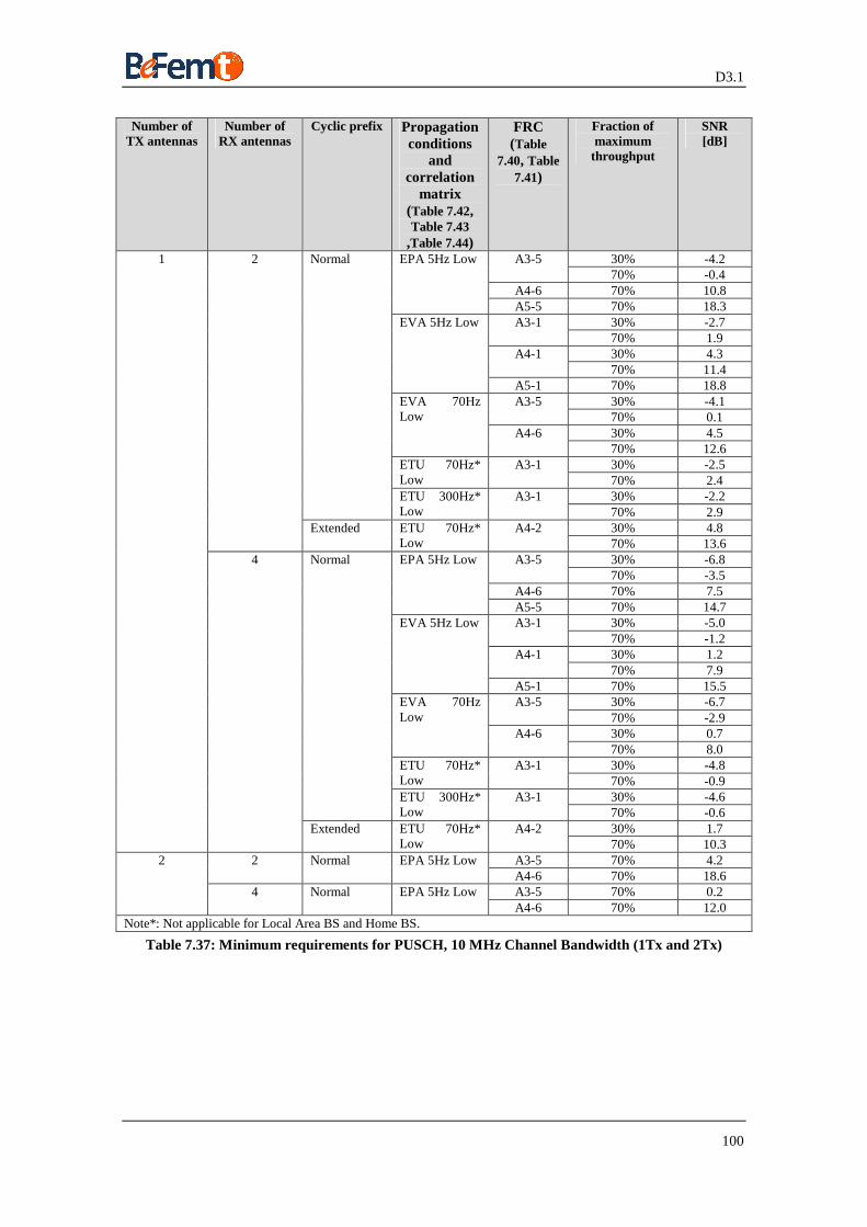
D3.1
100
Number of TX antennas
Number of RX antennas
Cyclic prefix Propagation conditions
and correlation
matrix (Table 7.42, Table 7.43
,Table 7.44)
FRC (Table
7.40, Table 7.41)
Fraction of maximum
throughput
SNR [dB]
30% -4.2 A3-5 70% -0.4
A4-6 70% 10.8
EPA 5Hz Low
A5-5 70% 18.3 30% -2.7 A3-1 70% 1.9 30% 4.3 A4-1 70% 11.4
EVA 5Hz Low
A5-1 70% 18.8 30% -4.1 A3-5 70% 0.1 30% 4.5
EVA 70Hz Low
A4-6 70% 12.6 30% -2.5 ETU 70Hz*
Low A3-1
70% 2.4 30% -2.2
Normal
ETU 300Hz* Low
A3-1 70% 2.9 30% 4.8
2
Extended ETU 70Hz* Low
A4-2 70% 13.6 30% -6.8 A3-5 70% -3.5
A4-6 70% 7.5
EPA 5Hz Low
A5-5 70% 14.7 30% -5.0 A3-1 70% -1.2 30% 1.2 A4-1 70% 7.9
EVA 5Hz Low
A5-1 70% 15.5 30% -6.7 A3-5 70% -2.9 30% 0.7
EVA 70Hz Low
A4-6 70% 8.0 30% -4.8 ETU 70Hz*
Low A3-1
70% -0.9 30% -4.6
Normal
ETU 300Hz* Low
A3-1 70% -0.6 30% 1.7
1
4
Extended ETU 70Hz* Low
A4-2 70% 10.3
A3-5 70% 4.2 2 Normal EPA 5Hz Low A4-6 70% 18.6 A3-5 70% 0.2
2
4 Normal EPA 5Hz Low A4-6 70% 12.0
Note*: Not applicable for Local Area BS and Home BS.
Table 7.37: Minimum requirements for PUSCH, 10 MHz Channel Bandwidth (1Tx and 2Tx)

D3.1
101
Number of TX antennas
Number of RX antennas
Cyclic prefix Propagation conditions
and correlation
matrix (Table 7.42, Table 7.43
,Table 7.44)
FRC (Table
7.40, Table 7.41)
Fraction of maximum
throughput
SNR [dB]
30% -4.5 A3-6 70% -0.8
A4-7 70% 11.3
EPA 5Hz Low
A5-6 70% 18.8 30% -2.8 A3-1 70% 1.8 30% 4.2 A4-1 70% 11.4
EVA 5Hz Low
A5-1 70% 18.7 30% -4.5 A3-6 70% -0.3 30% 4.2
EVA 70Hz Low
A4-7 70% 12.9 30% -2.5 ETU 70Hz*
Low A3-1
70% 2.4 30% -2.2
Normal
ETU 300Hz* Low
A3-1 70% 2.9 30% 4.9
2
Extended ETU 70Hz* Low
A4-2 70% 13.6 30% -7.2 A3-6 70% -3.8
A4-7 70% 7.6
EPA 5Hz Low
A5-6 70% 15.0 30% -5.0 A3-1 70% -1.2 30% 1.2 A4-1 70% 7.9
EVA 5Hz Low
A5-1 70% 15.7 30% -7.0 A3-6 70% -3.3 30% 0.7
EVA 70Hz Low
A4-7 70% 8.5 30% -4.8 ETU 70Hz*
Low A3-1
70% -1.0 30% -4.6
Normal
ETU 300Hz* Low
A3-1 70% -0.6 30% 1.6
1
4
Extended ETU 70Hz* Low
A4-2 70% 10.1
A3-6 70% 3.7 2 Normal EPA 5Hz Low A4-7 70% 19.4 A3-6 70% -0.2
2
4 Normal EPA 5Hz Low A4-7 70% 12.7
Note*: Not applicable for Local Area BS and Home BS.
Table 7.38: Minimum requirements for PUSCH, 15 MHz Channel Bandwidth (1Tx and 2Tx)
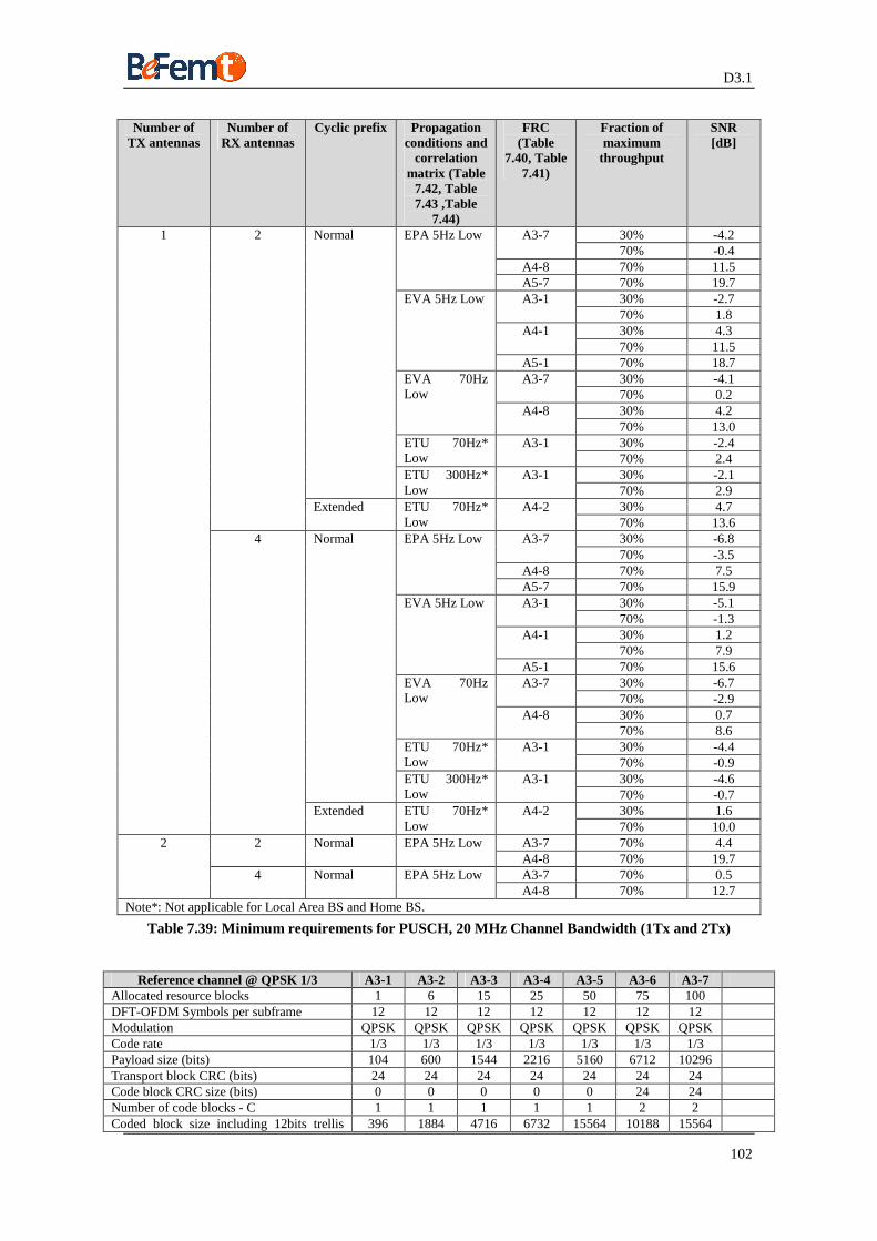
D3.1
102
Number of TX antennas
Number of RX antennas
Cyclic prefix Propagation conditions and
correlation matrix (Table
7.42, Table 7.43 ,Table
7.44)
FRC (Table
7.40, Table 7.41)
Fraction of maximum
throughput
SNR [dB]
30% -4.2 A3-7 70% -0.4
A4-8 70% 11.5
EPA 5Hz Low
A5-7 70% 19.7 30% -2.7 A3-1 70% 1.8 30% 4.3 A4-1 70% 11.5
EVA 5Hz Low
A5-1 70% 18.7 30% -4.1 A3-7 70% 0.2 30% 4.2
EVA 70Hz Low
A4-8 70% 13.0 30% -2.4 ETU 70Hz*
Low A3-1
70% 2.4 30% -2.1
Normal
ETU 300Hz* Low
A3-1 70% 2.9 30% 4.7
2
Extended ETU 70Hz* Low
A4-2 70% 13.6 30% -6.8 A3-7 70% -3.5
A4-8 70% 7.5
EPA 5Hz Low
A5-7 70% 15.9 30% -5.1 A3-1 70% -1.3 30% 1.2 A4-1 70% 7.9
EVA 5Hz Low
A5-1 70% 15.6 30% -6.7 A3-7 70% -2.9 30% 0.7
EVA 70Hz Low
A4-8 70% 8.6 30% -4.4 ETU 70Hz*
Low A3-1
70% -0.9 30% -4.6
Normal
ETU 300Hz* Low
A3-1 70% -0.7 30% 1.6
1
4
Extended ETU 70Hz* Low
A4-2 70% 10.0
A3-7 70% 4.4 2 Normal EPA 5Hz Low A4-8 70% 19.7 A3-7 70% 0.5
2
4 Normal EPA 5Hz Low A4-8 70% 12.7
Note*: Not applicable for Local Area BS and Home BS.
Table 7.39: Minimum requirements for PUSCH, 20 MHz Channel Bandwidth (1Tx and 2Tx)
Reference channel @ QPSK 1/3 A3-1 A3-2 A3-3 A3-4 A3-5 A3-6 A3-7 Allocated resource blocks 1 6 15 25 50 75 100 DFT-OFDM Symbols per subframe 12 12 12 12 12 12 12 Modulation QPSK QPSK QPSK QPSK QPSK QPSK QPSK Code rate 1/3 1/3 1/3 1/3 1/3 1/3 1/3 Payload size (bits) 104 600 1544 2216 5160 6712 10296 Transport block CRC (bits) 24 24 24 24 24 24 24 Code block CRC size (bits) 0 0 0 0 0 24 24 Number of code blocks - C 1 1 1 1 1 2 2 Coded block size including 12bits trellis 396 1884 4716 6732 15564 10188 15564
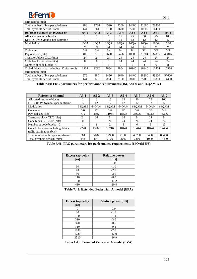
D3.1
103
termination (bits) Total number of bits per sub-frame 288 1728 4320 7200 14400 21600 28800 Total symbols per sub-frame 144 864 2160 3600 7200 10800 14400 Reference channel @ 16QAM 3/4 A4-1 A4-2 A4-3 A4-4 A4-5 A4-6 A4-7 A4-8 Allocated resource blocks 1 1 6 15 25 50 75 100 DFT-OFDM Symbols per subframe 12 10 12 12 12 12 12 12 Modulation 16QA
M 16QA
M 16QA
M 16QA
M 16QA
M 16QA
M 16QA
M 16QA
M Code rate 3/4 3/4 3/4 3/4 3/4 3/4 3/4 3/4 Payload size (bits) 408 376 2600 6456 10680 21384 32856 43816 Transport block CRC (bits) 24 24 24 24 24 24 24 24 Code block CRC size (bits) 0 0 0 24 24 24 24 24 Number of code blocks - C 1 1 1 2 2 4 6 8 Coded block size including 12bits trellis termination (bits)
1308 1212 7884 9804 16140 16140 16524 16524
Total number of bits per sub-frame 576 480 3456 8640 14400 28800 43200 57600 Total symbols per sub-frame 144 120 864 2160 3600 7200 10800 14400
Table 7.40: FRC parameters for performance requirements (16QAM ¾ and 16QAM ¾ )
Reference channel A5-1 A5-2 A5-3 A5-4 A5-5 A5-6 A5-7 Allocated resource blocks 1 6 15 25 50 75 100 DFT-OFDM Symbols per subframe 12 12 12 12 12 12 12 Modulation 64QAM 64QAM 64QAM 64QAM 64QAM 64QAM 64QAM Code rate 5/6 5/6 5/6 5/6 5/6 5/6 5/6 Payload size (bits) 712 4392 11064 18336 36696 55056 75376 Transport block CRC (bits) 24 24 24 24 24 24 24 Code block CRC size (bits) 0 0 24 24 24 24 24 Number of code blocks - C 1 1 2 3 6 9 13 Coded block size including 12bits trellis termination (bits)
2220 13260 16716 18444 18444 18444 17484
Total number of bits per sub-frame 864 5184 12960 21600 43200 64800 86400 Total symbols per sub-frame 144 864 2160 3600 7200 10800 14400
Table 7.41: FRC parameters for performance requirements (64QAM 5/6)
Excess tap delay [ns]
Relative power [dB]
0 0.0 30 -1.0 70 -2.0 90 -3.0 110 -8.0 190 -17.2 410 -20.8
Table 7.42: Extended Pedestrian A model (EPA)
Excess tap delay [ns]
Relative power [dB]
0 0.0 30 -1.5 150 -1.4 310 -3.6 370 -0.6 710 -9.1 1090 -7.0 1730 -12.0 2510 -16.9
Table 7.43: Extended Vehicular A model (EVA)
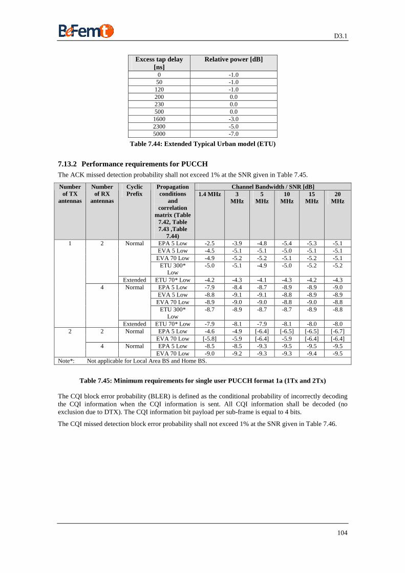
D3.1
104
Excess tap delay [ns]
Relative power [dB]
0 -1.0 50 -1.0 120 -1.0 200 0.0 230 0.0 500 0.0 1600 -3.0 2300 -5.0 5000 -7.0
Table 7.44: Extended Typical Urban model (ETU)
7.13.2 Performance requirements for PUCCH The ACK missed detection probability shall not exceed 1% at the SNR given in Table 7.45.
Channel Bandwidth / SNR [dB] Number of TX
antennas
Number of RX
antennas
Cyclic Prefix
Propagation conditions
and correlation
matrix (Table 7.42, Table 7.43 ,Table
7.44)
1.4 MHz 3 MHz
5 MHz
10 MHz
15 MHz
20 MHz
EPA 5 Low -2.5 -3.9 -4.8 -5.4 -5.3 -5.1 EVA 5 Low -4.5 -5.1 -5.1 -5.0 -5.1 -5.1 EVA 70 Low -4.9 -5.2 -5.2 -5.1 -5.2 -5.1
Normal
ETU 300* Low
-5.0 -5.1 -4.9 -5.0 -5.2 -5.2
2
Extended ETU 70* Low -4.2 -4.3 -4.1 -4.3 -4.2 -4.3 EPA 5 Low -7.9 -8.4 -8.7 -8.9 -8.9 -9.0 EVA 5 Low -8.8 -9.1 -9.1 -8.8 -8.9 -8.9 EVA 70 Low -8.9 -9.0 -9.0 -8.8 -9.0 -8.8
Normal
ETU 300* Low
-8.7 -8.9 -8.7 -8.7 -8.9 -8.8
1
4
Extended ETU 70* Low -7.9 -8.1 -7.9 -8.1 -8.0 -8.0 EPA 5 Low -4.6 -4.9 [-6.4] [-6.5] [-6.5] [-6.7] 2 Normal
EVA 70 Low [-5.8] -5.9 [-6.4] -5.9 [-6.4] [-6.4] EPA 5 Low -8.5 -8.5 -9.3 -9.5 -9.5 -9.5
2
4 Normal EVA 70 Low -9.0 -9.2 -9.3 -9.3 -9.4 -9.5
Note*: Not applicable for Local Area BS and Home BS.
Table 7.45: Minimum requirements for single user PUCCH format 1a (1Tx and 2Tx) The CQI block error probability (BLER) is defined as the conditional probability of incorrectly decoding the CQI information when the CQI information is sent. All CQI information shall be decoded (no exclusion due to DTX). The CQI information bit payload per sub-frame is equal to 4 bits.
The CQI missed detection block error probability shall not exceed 1% at the SNR given in Table 7.46.
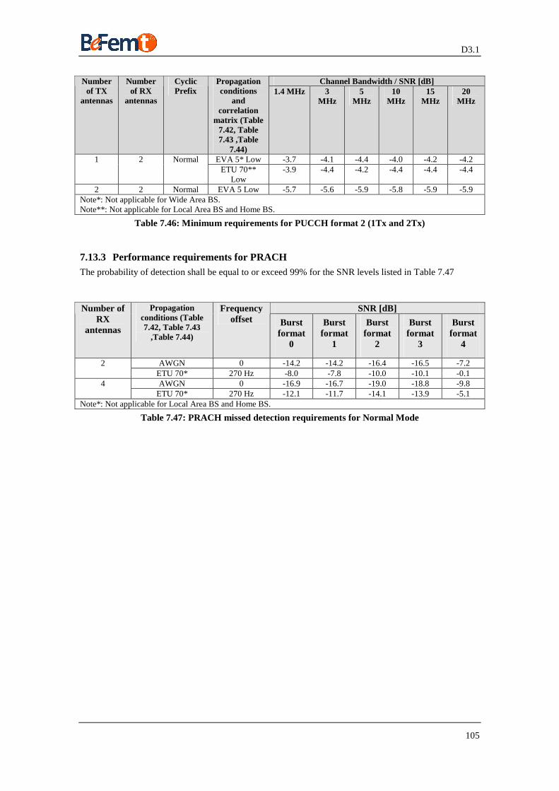
D3.1
105
Channel Bandwidth / SNR [dB] Number of TX
antennas
Number of RX
antennas
Cyclic Prefix
Propagation conditions
and correlation
matrix (Table 7.42, Table 7.43 ,Table
7.44)
1.4 MHz 3 MHz
5 MHz
10 MHz
15 MHz
20 MHz
EVA 5* Low -3.7 -4.1 -4.4 -4.0 -4.2 -4.2 1 2 Normal ETU 70**
Low -3.9 -4.4 -4.2 -4.4 -4.4 -4.4
2 2 Normal EVA 5 Low -5.7 -5.6 -5.9 -5.8 -5.9 -5.9 Note*: Not applicable for Wide Area BS. Note**: Not applicable for Local Area BS and Home BS.
Table 7.46: Minimum requirements for PUCCH format 2 (1Tx and 2Tx)
7.13.3 Performance requirements for PRACH The probability of detection shall be equal to or exceed 99% for the SNR levels listed in Table 7.47
SNR [dB] Number of RX
antennas
Propagation conditions (Table 7.42, Table 7.43
,Table 7.44)
Frequency offset Burst
format 0
Burst format
1
Burst format
2
Burst format
3
Burst format
4
AWGN 0 -14.2 -14.2 -16.4 -16.5 -7.2 2 ETU 70* 270 Hz -8.0 -7.8 -10.0 -10.1 -0.1 AWGN 0 -16.9 -16.7 -19.0 -18.8 -9.8 4
ETU 70* 270 Hz -12.1 -11.7 -14.1 -13.9 -5.1 Note*: Not applicable for Local Area BS and Home BS.
Table 7.47: PRACH missed detection requirements for Normal Mode