Embed Size (px)
Citation preview
339
Display and Imaging, Vol. 2, pp. 339–358Reprints available directly from the publisherPhotocopying permitted by license only
©2017 Old City Publishing, Inc.Published by license under the OCP Science imprint,
a member of the Old City Publishing Group
Inkjet Printing Technique and Its Application in Organic Light Emitting Diodes†
Amruth C1, BeAtA LuszCzynskA1*, BertrAnd G. r. dupont1 And zBiGniew sierAdzki2
1Department of Molecular Physics, Faculty of Chemistry, Lodz University of Technology, Zerom-skiego 116, 90-924 Lodz, Poland
2QWERTY Sp. z o.o., Siewna 21, 94-250 Lodz, Poland
Received: September 20, 2016. Accepted: October 27, 2016.
Development of printable and flexible Organic Light Emitting Diodes (OLEDs) might provide a path to the large and global production of dis-plays in the lighting market. A lot of research is being done in many fields like materials, equipment, processing methods, etc. to make this technology cheaper and more efficient. This article unveils the inkjet printing technique and its challenges for printed, cost-effective OLEDs. Firstly, to understand the inkjet printing mechanism, various rheological parameters involved in inkjet printing and ink formulation have been discussed. Then, the interac-tion between the ink and the substrates were introduced, and solutions to avoid the commonly observed “coffee-ring” structure were reviewed. A summary of the recent progress in inkjet printing of polymers and small molecules in OLED devices was also given and other techniques such as aerosol and electrohydrodynamic jet printing, which open up alternative depositing method were discussed. Finally, the challenges involved in the printing of large area displays on an industrial scale were presented.
Keywords: Printable Electronics, Organic Electronics, inkjet, OLEDs, ink formulation, thin film.
1. INTRODUCTION
Organic Light Emitting Diodes (OLEDs) are the most promising devices used to fabricate displays and solid-state lighting [1, 2]. According to a recent
*Corresponding author E-mail: [email protected]†The research leading to these results received funding from the H2020-MSCA-ITN-2015/674990 project “EXCILIGHT”.
340 Amruth C et al.
IDTechEx market analysis, within the next five years, display and lighting markets together will reach $18 billion [1, 2]. A lot of research focuses on making OLEDs more robust, stable and cheaper.
The OLED technology is unique over other display and lighting products because of its high brightness, large viewing angle and low power consump-tion. Several fabrication techniques can be used to produce such devices. Currently, OLEDs are successfully produced by means of evaporation tech-niques for television and mobile phone applications. However, there are still many challenges in the fabrication of larger size and economical displays.
Currently, inkjet, gravure, screen and flexography printers are commonly used for printing electronic materials and devices. Among these printing techniques, inkjet seems to be the most promising technique for OLEDs fab-rication because of its high resolution, non-contact method, minimal material waste, highly precise drop positioning and high speed. The inkjet technology has already drawn attention to mass production: the Kateeva company [3] designed a YIELDjet FLEX printer for printing large area flexible OLEDs in large quantities.
In this work, we have described the most important challenges involved in the inkjet printing technology for printing functional material on the different surface and the current progress for the production of OLEDs.
2. INKJET PINTER AND ITS CLASSIFICATION
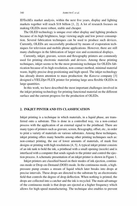
Inkjet printing is a technique in which materials, in a liquid phase, are trans-ferred onto a substrate. This is done in a controlled way, via a non-contact process with the application of an external signal to the printhead. There are many types of printers such as gravure, screen, flexography, offset, etc., in order to print a variety of materials on various substrates. Among these techniques, inkjet printing offers many benefits among other printing techniques such as: non-contact printing, the use of lower amounts of materials, of mask free designs or printing with high resolutions [4, 5]. A typical inkjet printer consists of an ink tank to hold the ink, a printhead with a small opening (nozzle) and is interfaced with a computer that sends signals to the printer and control the ejec-tion process. A schematic presentation of an inkjet printer is shown in Figure 1.
Inkjet printers are classified based on their modes of ink ejection, continu-ous mode or Drop-on-Demand (DOD) mode. In the continuous mode, a high-pressure pump creates a stream of liquid which later breaks into drops at precise intervals. These drops are directed to the substrate by an electrostatic field that controls the degree of drop deflection. When nothing is printed, the drops are collected into a catcher and the ink is recycled. The main advantage of the continuous mode is that drops are ejected at a higher frequency which allows for high-speed manufacturing. The technique also enables to prevent
inkjet printinG teChnique And its AppLiCAtion in orGAniC 341
nozzle clogging which will favor the use of low volatile solvents like ketones or alcohols [6, 7, 8, 9].
With DOD the ink drops are ejected on demand. DOD printers are named according to their actuators: either piezoelectric or thermal printers. Thermal printers use small heaters, which heat the liquid upon the application of a cur-rent and create bubbles inside the print head. These bubbles increase the pres-sure inside the printing chamber and push the ink onto the substrate. Because of the elevated applied temperature, only a limited number of solvents can be printed and the print head often requires to be replaced with new ones [10].
Piezoelectric printers use piezoelectric elements (such as ceramics) to convert an electric signal into a pressure pulse inside the printing chamber. The pressure inside the printing chamber forces the ink out of the nozzle and initiates the printing process. Piezoheads are able to produce small drops of less than 1picoliter, and print with a high accuracy (5 µm) [3, 4, 6, 10].
Piezoelectric printers are usually preferred for printing OLEDs and other organic electronic devices since they offer the selection of multiple solvents and the formation of variable drop volumes (from 1pl to 100pl). Additionally, because of the low temperature of the head, the ink will be stable throughout the printing process. Thermal printers on the other hand are limited to water based solvents because of the elevated temperatures used in the process [10].
3. PHYSICAL PROPERTIES OF THE INKS
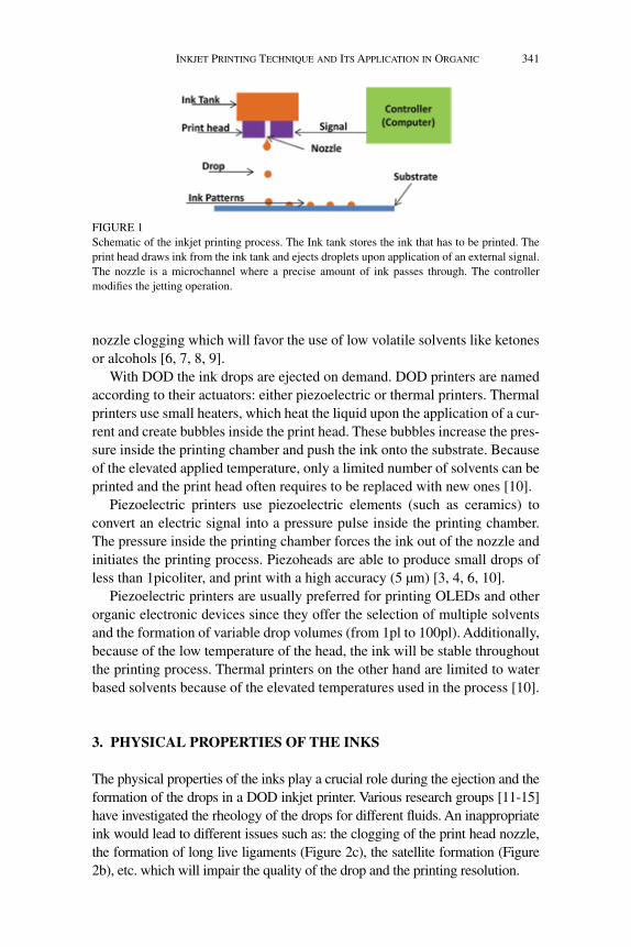
The physical properties of the inks play a crucial role during the ejection and the formation of the drops in a DOD inkjet printer. Various research groups [11-15] have investigated the rheology of the drops for different fluids. An inappropriate ink would lead to different issues such as: the clogging of the print head nozzle, the formation of long live ligaments (Figure 2c), the satellite formation (Figure 2b), etc. which will impair the quality of the drop and the printing resolution.
FIGurE 1Schematic of the inkjet printing process. The Ink tank stores the ink that has to be printed. The print head draws ink from the ink tank and ejects droplets upon application of an external signal. The nozzle is a microchannel where a precise amount of ink passes through. The controller modifies the jetting operation.
342 Amruth C et al.
There are two main physical quantities that determine the drop behaviour: the surface tension and the viscosity [16]. To study the drop ejection from the print head, Fromm [17] developed two dimensionless numbers, which are solutions of the Navier-Stokes equation. In a moving fluid, the reynolds number (re) is the ratio between the inertial and the viscous forces, and the Weber number (We) is the ratio between the inertia and the surface tension.
Re = ρηVd
(1)
We = ργ
V d2
(2)
Where, ρ, V, d, η and γ are the density of the fluid, the velocity, the char-acteristic length (i.e., the radius of the nozzle), the viscosity and the surface tension respectively.
Another, dimensionless number, the Ohnesorge number (Oh), was devel-oped by removing the velocity term in the above two equations. It corre-sponds to the ratio between the reynolds number (re) and the square root of the Weber number (We).
Some groups [17-19] use the symbol Z corresponding to (1/Oh), which is the inverse of the Ohnesorge number. This Z value allows to predict when the liquid can be efficiently printed. Fromm [17] argued that only when Z> 2, a steady drop is formed from DOD printers. There is still a debate among the scientific community concerning the relevance of the Z value for printing. In 2009, Jang et al. [19] determined the printability
FIGurE 2Image of the drop formation of polymer ink obtained from a Dimatix material printer. The upper drops on the figures are reflections of the ejected drops. (a) Ideal spherical drop for tuned opti-mised fluids, (b) Satelite formation for higher ink Z values (c) Long live Ligaments for low ink Z values. For an optimised ink, the distance between the desired spherical drops and the nozzle was 570 µm (see Figure 2a).
inkjet printinG teChnique And its AppLiCAtion in orGAniC 343
range for the Z value to be between 4 and 14. This was extracted by observing the dynamic of the droplet formation for different fluids having various Z values. Additionally, they considered characteristics such as: (1) the single drop formability, (2) the distance between the nozzle and the substrate, (3) the position accuracy and (4) the maximum allowable frequency to quantify the drop stability. For lower Z values, a long live ligament formation was observed along with an increased single drop for-mation time. This lead to an inaccurate placement of the drop. For higher Z values, undesirable satellites were formed due to the facilitated droplet ejection without any viscous dissipation. Singh et al. [20] have demon-strated the inkjet printing of the conducting polymer poly(3,4-ethylenedioxidethiophene)-polystyrenesulfonic acid (PEDOT: PSS) for solar cell applications. They found for the Z value of 4.63 and 5.37, the spherical drop was formed after an elapsed time of 45 µs and 65 µs respec-tively. Nevertheless, it is necessary to notice that few research groups have reported a reasonable drop stability for fluids with physical proper-ties outside of the conventional range of 1<Z<14 [21-25].
4. SUBSTRATE INTERACTION WITH THE INK
Printed organic electronic devices are generally made of various functional patterns, which are printed layer by layer, on different substrates [26-34]. In the organic electronic field of research devices require a very high active layer quality in order to demonstrate high efficiencies, hence the printing of these devices will have to be highly homogeneous. This will be one of the most important challenge for inkjet printed devices. For example, the nonuni-formity in the thickness of OLEDs layers resulted in lesser current and bright-ness demonstrated by Yoshioka et al. [34]. Therefore, understanding the behaviour of such inks on various substrates or previously printed layers is necessary.
Generally, upon drying, the inkjet printed material will migrate towards the edges of the substrate. The printing will, therefore, present an increased thickness at the edges differing by an approximate factor of ten from the printed middle. This phenomenon has been widely reported and is referred to as the “coffee-ring” effect [35]. This phenomenon is detrimental to the per-formance of printed organic electronic devices as it decreases the printed resolution, increases the material consumption, reduces the lifetime of the devices, etc. It is the consequence of the convective flow originating from the evaporation of the droplets at the pinned edge (immobilized edge) [36-38]. Many factors can affect the “coffee ring” effect, namely the wetting behav-iour of ink on the substrate, the particles influence inside the ink, the surface energy and temperature of the substrate, etc. This effect finds its origin in the
344 Amruth C et al.
following two phenomena: (1) the printed edge that is being pinned and (2) the evaporation at the printed edge.
Some methods exist to avoid this effect and each of them depends on spe-cific applications:
(a) The first method is the electrowetting, where an AC electric field is applied to the ink drop that induces the line edge to oscillate and hence does not involve pinning. However, it is a difficult method to apply to an industrial scale since it involves high-frequency AC voltages [39].
(b) Secondly, Shen et al. [40] found that below a drop diameter of 10µm there will be no “coffee ring” effect. This is because of the quick evaporation of solvent for smaller drop sizes and the particles inside the ink will not have time to migrate to the edge.
(c) Alternatively, increasing the evaporation rate at the centre in a closed environment will decrease the “coffee ring” effect due to an inward flow of materials counteracting the outward flow [41].
(d) Lastly, the most promising method so far consist in the optimising mechanism of evaporation (the outward capillary effect and the inward flow of materials) [41]. The equation 3 is the expression of the Marangoni number (Ma) which represents the Marangoni flow (flow driven by surface tension difference).
Mar
D=
∆γη
(3)
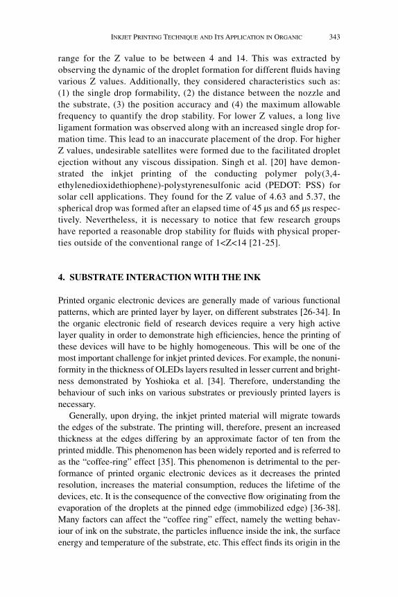
Where ∆γ is surface tension difference between the centre of the drop and the edge, r is a radius of the drop, η is the fluid viscosity and D the particle diffusion constant. When the Marangoni flow is inward, then it counteracts the outward capillary effect which results in a more homogeneous surface profile of the dried drops and hence a less intense coffee ring effect [42-43]. The flows can be altered by several means such as: (1) changing the solvent mixture,(2) modifying the surface energy, (3) adding surfactants, (4) influ-encing the drying time (5) modifying the capillary properties etc. [44-51].
A solvent mixture is usually used in the literature for the printing of organic electronic devices in order to obtain an improved thin film morphol-ogy and device performance. Liu et al. [52] demonstrated the printing of small organic molecules for display applications. A uniform film was obtained by inducing a surface tension difference that would favour the inward Maran-goni flow. A low volatile solvent DMA (3,4-dimethylanisole) was used to dissolve small organic molecules. The surface tension of the DMA solution was decreased from 30.2 mN/m to 23.6 mN/m upon the addition of the small molecules. Then they mixed an optimised amount of the highly volatile sol-vent, P-xylene (P-xy), to the DMA solution. Since the surface tension of the DMA solution is lower than the P-xy, an inward Marangoni flow was created
inkjet printinG teChnique And its AppLiCAtion in orGAniC 345
in the printed ink. Finally, by adjusting the volume ratio of the solvents, a flat film profile was obtained. Figure 3 presents the schematic solvent evapora-tion, the outward capillary flow related to the DMA solution and the counter Marangoni flow related to the P-xy solvent.
Similarly, Grimaldia et al. [53] also used a solvent mixture to form a uni-form film of n-type semiconductor (perylene diimide (PDI-8CN2)) on silicon for the fabrication of Organic Thin Film Transistors (OTFT). They investi-gated the film quality: by dissolving the n-type semiconductor in different ratios of 1, 2- dichlorobenzene (DCB) and chloroform (CH). They demon-strated that the OTFTs with the active layers obtained from a mixture of sol-vents with a ratio of 3:2 (DCB:CH) had higher mobility.
The surface energy of the substrate is also a fundamental parameter to take into account in order to improve the quality of the printed film. Ely et al. [54] have investigated the wetting behaviour of a printed PEDOT: PSS ink inside an Su-8 photo-resist (glycidyl ether of bisphenol-A novalac [55]) well on an ITO coated glass substrate. They printed PEDOT: PSS after different surface treatments such as oxygen plasma, (3-aminopropyl)triethoxysilane (APTS) liquid treatment, APTS vapour treatment and on an untreated substrate. They found that for all the treated surfaces the quality of the film was improved when compared to the untreated ones. However, the films printed on oxygen treated substrates (which presented the highest surface energy) showed smoother and more uniform morphologies than the lower surface energy sub-strates.
Similarly, Li et al. [56] explored the wetting behaviour of highly diluted solutions (of copper(II) sulfate, cobalt(II) sulfate, glucose (monosaccharide), cellobiose (disaccharide), poly(ethylene glycol) 20K (PEG), Dextran 500K (polysaccharide), poly(vinyl alcohol) 130K (PVA), poly(vinyl pyrrolidone) 360K (PVP), sodium polystyrene sulfonate 70K (NaPSS), poly(diallyldimethylammonium chloride) (PDDC)) on various substrates and obtained different drop patterns. They showed that different contact angles between the solutions and the substrates produced various patterns after drying. For a small contact angle, a concentrated stain (material concentrated in the
FIGurE 3Schematic illustration of the capillary and Marangoni flows induced by the surface tension gradi-ent during the solvent evaporation.
346 Amruth C et al.
centre of the drop) was obtained instead of the “coffee ring” effect. This was explained by the presence of surface-inactive solutes in the ink that presented small contact angles with the substrates and were deposited at the final stage of the film formation. For large contact angles, the presence of a “coffee ring” effect was obvious. The effect could be explained by a lower material with-drawal rate when compared to the deposition rate at the edge. Furthermore, when considering a mixture of surface-active and surface-inactive solutes, con-centric rings were formed. These were caused by the two solutes respectively.
Alternately, in 2013, Friederich et al. [57] showed that the “coffee ring” effect could be avoided by modifying the viscosity of the ink and the drying time. They prepared an original ink by dissolving barium strontium titanate in butyl diglycol. Ethyl cellulose and isopropyl alcohol were then used to change the viscosity and the drying time of the printed patterns. The printed film with the larger amount of ethyl cellulose did not show any “coffee ring” effect because of the high viscosity of the ink. It, however, took a longer time to dry. Consequently, the authors added a large amount of isopropyl alcohol in order to shorten the drying time, but a “coffee ring” effect was observed. An improved film quality was therefore obtained by optimizing the amount of ethyl cellulose and isopropyl alcohol in the ink.
An additional way of addressing the “coffee ring” effect is obtained by modulating the environmental conditions around the printed films. Fukuda et al. [58] studied the influence of humid conditions on the printed film mor-phology. In this work, the conditions for the printing of alcohol based silver inks were optimised. Silver electrodes were printed and dried at different humidity conditions: 30%, 80%, 85% and 90% for 30 min at 30 °C. For the lower humid conditions, a “coffee ring” effect was observed due to the fast evaporation rate and the high capillary flow. In contrast, for the higher humid conditions, the “coffee ring” effect disappeared, since the convex morphol-ogy dominated with a slower evaporation rate. The humidity level of 85% was found to give the best film quality for transistor applications.
Most recently, Eales et al. [59] studied the quality of printed light emitted films by varying the capillary number. The capillary number was changed by using various amounts of polymer contents in the functional inks. A higher capillary number was obtained for a higher polymer concentration and simi-larly a lower capillary number for lower concentrations. Consequently, there was no “coffee ring” effect for lower capillary inks because of a high viscos-ity. However, for the higher capillary inks, a more prominent “coffee ring” effect was observed because of a lower solid content.
5. INKJET PRINTING OF OLEDS
OLEDs are devices which emit light when a current is flown through them. Typically, OLEDs are composed of an Emissive Layer (EML) sandwiched
inkjet printinG teChnique And its AppLiCAtion in orGAniC 347
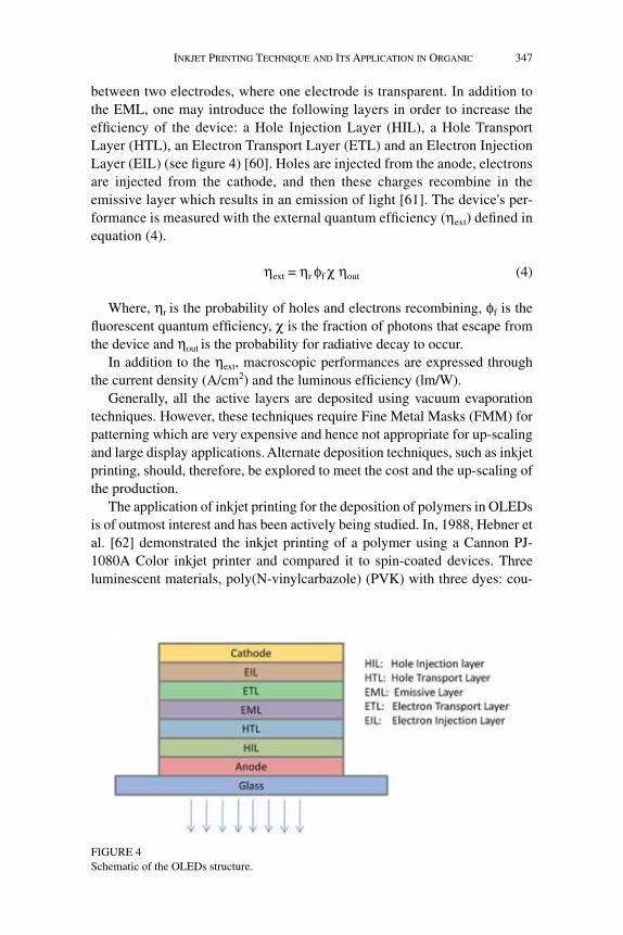
between two electrodes, where one electrode is transparent. In addition to the EML, one may introduce the following layers in order to increase the efficiency of the device: a Hole Injection Layer (HIL), a Hole Transport Layer (HTL), an Electron Transport Layer (ETL) and an Electron Injection Layer (EIL) (see figure 4) [60]. Holes are injected from the anode, electrons are injected from the cathode, and then these charges recombine in the emissive layer which results in an emission of light [61]. The device's per-formance is measured with the external quantum efficiency (ηext) defined in equation (4).
ηext = ηr φf χ ηout (4)
Where, ηr is the probability of holes and electrons recombining, φf is the fluorescent quantum efficiency, χ is the fraction of photons that escape from the device and ηout is the probability for radiative decay to occur.
In addition to the ηext, macroscopic performances are expressed through the current density (A/cm2) and the luminous efficiency (lm/W).
Generally, all the active layers are deposited using vacuum evaporation techniques. However, these techniques require Fine Metal Masks (FMM) for patterning which are very expensive and hence not appropriate for up-scaling and large display applications. Alternate deposition techniques, such as inkjet printing, should, therefore, be explored to meet the cost and the up-scaling of the production.
The application of inkjet printing for the deposition of polymers in OLEDs is of outmost interest and has been actively being studied. In, 1988, Hebner et al. [62] demonstrated the inkjet printing of a polymer using a Cannon PJ-1080A Color inkjet printer and compared it to spin-coated devices. Three luminescent materials, poly(N-vinylcarbazole) (PVK) with three dyes: cou-
FIGurE 4Schematic of the OLEDs structure.
348 Amruth C et al.
marin 6 (C6), coumarin 47 (C47), and nile red were used for the preparation of OLEDs. The photoluminescence spectra of the printed and spin-coated films demonstrated similar shapes and magnitudes. A current density of 1 mA/cm2 was measured at a voltage of 7 V for the spin-coated devices, and at various voltages going from 6 to 11 V for the ink-jet printed devices. The authors deducted that the printed devices were less efficient than the spin-coated devices since their luminescence vs current measurements differed by a factor of 2. They attributed this reduction in performance to a bad film morphology in the case of the printed devices.
Villani at al. [63] fabricated OLEDs by inkjet printing an HTL (poly(9,9-dihexyl-9H-fluorene-2,7-diyl)) (PF6)) with the following device structure: PET/ITO/PF6/Alq3/Al (Alq3 was used here as an ETL and EML). The HTL was printed with a thickness of 50 nm on a piranha treated substrate and 100 nm on untreated substrates. The treated substrates presented a higher rough-ness, because of the small contact angle between the active layer and the ITO and because of the presence of a thin liquid layer near the drop edge. Three sets of samples were made: (1) one with an inkjet printed layer of PF6, (2) one with a thin layer (15 nm) of spin-coated PF6, and (3) one with a thick layer (60 nm) of spin-coated PF6. The current-voltage (I-V) measurements showed electrical threshold values of: 5.3 V for the thinner spin-coated films, 8.1 V for the inkjet printed devices and 25.6 V for the thicker spin-coated films. Hence, the I-V measurements revealed that the inkjet printed character-istics were similar to the device prepared by spin coating with a thinner HTL. This could be explained by the fact that the non-uniform thickness of the inkjet drops created preferential paths for the current to flow since generally speaking the resistance is lower across a thinner area of the film. The authors, however, indicated that it is hard to compare the two technologies since inkjet printed devices present a higher thin film variability than spin-coated devices.
Similarly, Olivier et al. [64] compared the printing of two polymers in OLEDs to devices fabricated using vacuum evaporation and spin coating techniques. Table 1 describes OLEDs with layers deposited with different techniques and classified as A, B, C and D depending on the method used to deposit the active layers. As expected, a uniform light output was obtained from device A (with vacuum-deposited layers) and the illumination was homogeneous (see table 1). At 3.5 V, the current efficiency and maximum luminous efficiency were 11.6 cd/A and 9.7 lm/W respectively. Devices B and C showed a uniform light output but black spots were observed because of the solution process deposition techniques that influence the HIL and the HTL. The I-V characteristics of devices A, B and C showed a typical diode behaviour. However, for device D where the layers were inkjet printed, the light emission was not uniform and the materials were unevenly dispersed. The I-V characteristic did not follow a standard diode behaviour. The bright-ness (less than 10 cd/m2) and the efficiencies (0.008 cd/A and 0.003 lm/W at 10 V).) were low when compared to the rest of the devices. Employing print-
inkjet printinG teChnique And its AppLiCAtion in orGAniC 349
ing techniques for more than one layer resulted in the decrease of the device performances.
Teichler et al. [65] also demonstrated the inkjet printing of three chemically altered light emitting polymers (red, green and blue) for the production of OLEDs. The turn-on voltages for the red and the green OLEDs were above 10V. However, no light output was observed for the blue emitting devices. This was probably due to the large band gap of the blue emitting polymer (poly-(fluorene-phenylene)) that demanded a higher operational voltage and therefore degraded faster. In addition, oxygen was responsible for short-circuiting the blue OLEDs. In this study, large area OLEDs of 20 mm ×30 mm were also printed with a single noz-zle. However, some part of the film dried before the completion of the entire printing, which resulted in a non-uniform layer. The authors, therefore, men-tioned that by using multi-nozzles one would increase the film quality.
Having reviewed the inkjet printing of different polymers, the focus will now be brought on an alternative for the design of printed OLEDs: small molecules.
In the work of Coenen et al. [66] two emitter small molecules were inkjet printed for the fabrication of OLEDs. First PEDOT:PSS and then a thermally cross-linkable HIL were printed on ITO coated glass substrates. Then, two colours, green and red were printed side by side and a thin film of 80nm was obtained. The brightness of the green and the red OLEDs at a voltage of 5.5 V and current of 5.0 ± 0.1 mA was 300 cd/m2 and 500 cd/m2 respectively. The luminescence, at the interface between the two emissive layers was weak and not uniform. This was due to the dissolution of the first printed layer by the second printed layer. Therefore, the authors suggested that the printing of the two layers should be done simultaneously in order to reduce the mixing of the lateral layers and thus improve the light output.
Likewise, Gorter et al. [67] also demonstrated the inkjet printing of small molecules that were synthesized for vacuum deposition processes. HTL (PEDOT: PSS) and HIL ((α-NPD, N,N′-Di-[(1- naphthyl)-N,N′-diphenyl]-1,1′-biphenyl)-4,4′-diamine)) layers were also printed and the devices were compared to small molecules OLEDs produced by vacuum deposition. The
TABLE 1Devices made with different fabrication techniques (reproduced from Olivier et al. [64] with permission) from the Society of Photo Optical Instrumentation Engineers and the authors.
Device HIL HTL EML
A STTB:F4TCNQ* NPB* TCTA:Ir(mppy)3 *
B PEDOT-PSS** NPB* TCTA:Ir(mmpy)3 *
C PEDOT-PSS** QuPD*** TCTA:Ir(mppy)3*
D PEDOT-PSS** QuPD*** f-CHO-Acr3***
*Deposited by vacuum evaporation **Deposited by spin coating ***Deposited by inkjet printing.
350 Amruth C et al.
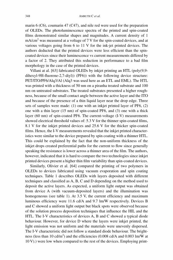
device structures for both deposition techniques is shown in Figure 5. The luminescence, the leakage current and the efficiency of devices with all evap-orated layers was better when compared to devices where at least one layer was inkjet printed (see table 2). Overall, the quality of the light emission appeared to be generally worse with inkjet printed layers, and as expected, devices with more vacuum-deposited layers showed better performances. The authors mentioned that the poor quality of the Alq3 inkjet-printed layers or the dissolution of α-NPD one, was responsible for the relatively low effi-ciency of the devices as well as the high leakage current.
Jung et al. [68] also demonstrated the inkjet printing of organic phospho-rescent small molecules. 5 wt.% of tris(2-phenylpyridine)iridium(III) (Ir(ppy)3) doped in 4,4′-Bis(carbazol-9-yl)biphenyl (CBP) was used as a light emitting material. Only the emissive layer was printed and the rest of the layers were vacuum deposited. Four devices were fabricated. They were made of different HTL: 4,4′,4″-tris(N-(2-naphthyl)-N-phenylamino)-triphe-nylamine (2-TNATA), N,N′-bis(naphthalen-1-yl)-N,N′-bis(phenyl)-benzidine (NPB), di-[4-(N,N-ditolyl-amino)-phenyl]cyclohexane (TAPC),
FIGurE 5Schematic of the device structure.
TABLE 2Devices made with different fabrication techniques (reproduced from Gorter et al [67] with permission) from Elsevier.
SamplePEDOT:PSS(HIL)
α-NPD (HTL) Alq3 (EML)
Leakage current
Luminous Efficiency
Cd/A Lm/W
1 None Evaporation Evaporation 147 4.2 1.5
1A CH8000 Evaporation Evaporation 0.9 2.6 2.3
2 CH8000 Evaporation Inkjet 0.14 0.6 0.35
3 HIL1005 Inkjet Evaporation 639 1.7 1.0
3B HIL1005 Inkjet Evaporation 126 3.2 1.5
3C CH8000 Inkjet Evaporation 0.0019 3.1 2.6
4 HIL1005 Inkjet Inkjet 367 <<0.1 << 0.1
inkjet printinG teChnique And its AppLiCAtion in orGAniC 351
and 4,4′,4″-tris(carbazol-9-yl)triphenylamine (TCTA). Measurements showed that the current density and the luminous efficiency of the printed devices were similar to the devices made by vacuum deposition. Further-more, they observed that the devices fabricated, by incorporating TCTA as a HTL, displayed a highest current efficiency of 40 Cd/A (EQE=11.7%) than the rest of the devices. This is because TCTA is a slow electron transporting material and has the highest triplet overlap with the emitter material. Addi-tionally, the authors mentioned that the printed devices gave unexpected light out-coupling, which may be due to the roughness of the printed layer.
In order to give a complete overview of the inkjet printed OLED technolo-gies, one also need to study several jet printing techniques. Instead of the com-monly used piezoheads for inkjet printing, other jet printers like an aerosol jet and electrohydrodynamic jet printers have been investigated for the printing of OLEDs. Tait et al. [69] used an aerosol jet technique to print a 144 pixel per inch (ppi) OLEDs display. The PVK was used as the host material. Bis(2methyldibenzoquinoxaline)(acetylacetonate)iridium(III(Ir(MDQ)2acac), tris(2phenylpyridine)iridium(III) (Ir(ppy)3), and 2,5,8,11-tetra-tert-butylper-ylene (TBPe) were used as guest dyes to emit red, green and blue light respec-tively. After modifying, the various printing parameters such as the gas flow rate, the jetting speed and the substrate temperature, a very thin line of 30 nm and a narrow width of 30 µm was printed. Electroluminescent peaks of 475, 520, 590 nm for blue, green and red were observed, respectively. This work shows that aerosol jet printers have the potential to be adopted for high-resolu-tion OLED printing.
Kim et al. [70] demonstrated the fabrication of OLEDs using another printing technique, high-resolution electrohydrodynamic inkjet printing. A small molecule, 5 wt% of 4,4′-bis[4-(di-p-tolylamino)styryl]biphenyl (DPAVBi) doped with 2-tert-butyl-9,10-di(naphth-2-yl)anthracene (TBADN), was used as an emitting material. Here, only the active layer was printed. High-resolution features of 5µm with a uniform surface morphology were obtained. The turn-on voltage and the maximum luminescence for the devices were 4.5 V and 17 000 cdm-2 respectively. The maximum current efficiency and the external quantum efficiency were 8.7 cd A−1 and 4.6% respectively. These results indicate the successful printing of OLEDs by electrohydrody-namic inkjet printing and the potential for future application for the fabrica-tion of OLEDs with other functional layers.
Another fundamental aspect of the presented technology is the commer-cial perspective. Besides the laboratory studies, there are some challenges involving mass production of inkjet printed OLED panels. Chen et al. [71] fabricated a 200 ppi OLED panel with the inkjet printing technique. The device structure is shown in Figure 6. All the layers were inkjet printed except for aluminum, which was deposited by thermal evaporation. The authors dis-cussed two major challenges for printing high-density display panels. First, the Total Position Accuracy (TPA), which depends on three parameters,
352 Amruth C et al.
namely the machinery accuracy (M) that can extend up to 5µm, the angle between the nozzle and the line of sight (θ), and the distance between the nozzle and the substrate (d). These parameters can be found in equation (5), which is the expression of the TPA. When the θ value decreases to zero, the positional accuracy can be simplified to the machinery error only.
TPA M d= + ∏2 22 360( / )θ (5)
The second parameter is the “drop volume” that controls the resolution and the sharpness of the pixel. A 200 ppi panel needs the drop diameter to be less than 34.5 µm. Therefore, a 7 picoliter drop volume was chosen to make the drop diameter less than 34.5 µm. According to the authors, the machinery error has to be reduced in order to fabricate high-resolution OLED panels, because other parameters can be made negligible.
Later, the same group [72] demonstrated the inkjet printing of a 65-inches OLED panel and studied the annealing conditions of the printed films. It was found that annealing in one step with a low speed leads to an inferior film quality because of the formation of a “coffee ring” effect. However, a film of higher quality was obtained with multiple drying steps for a short period of time.
Finally, to conclude this overview of inkjet printed OLEDs, new aspects of the technology will be considered. Some reports demonstrated that the printing technique may also be useful for complicated emissive systems. Verma et al. [73] recently applied the inkjet printing method to NHetPHOS (N-heterocycle-phosphine) displaying the Thermally Activated Delayed Fluorescence (TADF) property. The obtained OLEDs were characterized by a low turn-on voltage of 4 V and a current efficiency of 45 Cd/A corre-sponding to 13.9 ±1.9 % ηext. However, the nonlinear nature observed in the luminance–efficiency plot hinted that the charge carrier balance of the device needed to be improved. Additionally, the authors suggested that with alteration of the surface roughness one could enhance the device perfor-mances [74].
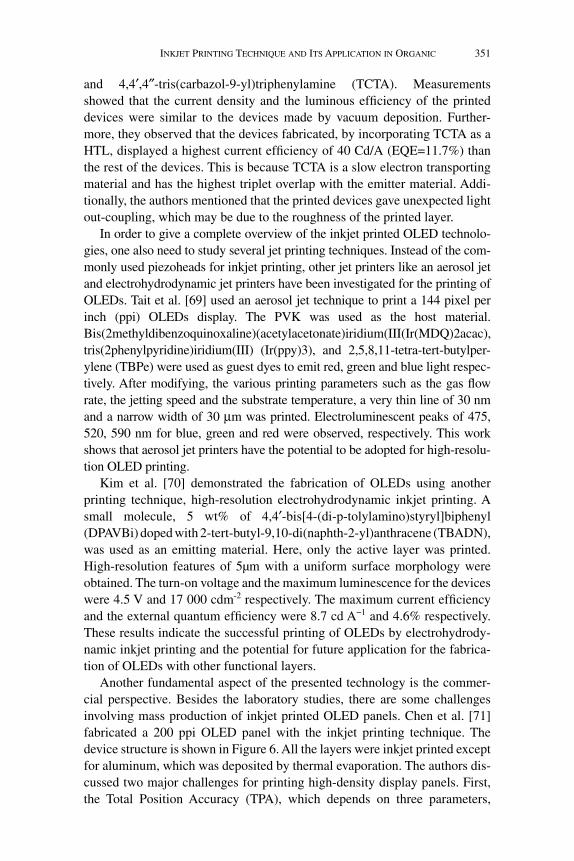
FIGurE 6Schematic of the device structure (reproduced from Chen et al. [71] with permission) from John Wiley and Sons.
inkjet printinG teChnique And its AppLiCAtion in orGAniC 353
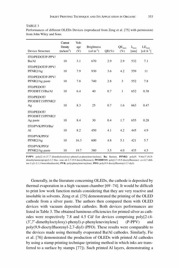
Generally, in the literature concerning OLEDs, the cathode is deposited by thermal evaporation in a high vacuum chamber [69 -74]. It would be difficult to print low work function metals considering that they are very reactive and insoluble in solvents. Zeng et al. [75] demonstrated the printing of the OLED cathode from a silver paste. The authors then compared them with OLED devices with vacuum deposited cathodes. Both devices performances are listed in Table 3. The obtained luminous efficiencies for printed silver as cath-odes were respectively 7.8 and 4.5 Cd/ for devices comprising poly[2-(4-(3′,7′-dimethyloctyloxy)-phenyl)-p-phenylenevinylene] (P-PPV) and poly(9,9-dioctylfluorenyl-2,7-diyl) (PFO). These results were comparable to the devices made using thermally evaporated Ba/Al cathodes. Similarly, Fie et al. [76] demonstrated the production of OLEDs with printed Al cathodes by using a stamp printing technique (printing method in which inks are trans-ferred to a surface by stamps [77]). Such printed Al layers, demonstrating a
TABLE 3Performances of different OLEDs Devices (reproduced from Zeng et al. [75] with permission) from John Wiley and Sons.
Device Structure
Current Density
(mAcm-2)
Volt-age (V)
Brightness (cd m-2) QE(%)
QEmax
(%)λmax
[nm]LEmax
[cd A-1]
ITO/PEDOT/P-PPV/Ba/Al 10 3.1 670 2.9 2.9 532 7.1
ITO/PEDOT/P-PPV/PFNr2/Ag 10 7.9 930 3.6 4.2 559 11
ITO/PEDOT/P-PPV/PFNr2/Ag paste 10 7.8 740 2.8 3 552 7.8
ITO/PEDOT/ PFODBT15/Ba/Al 10 6.4 40 0.7 1 652 0.38
ITO/PEDOT/ PFODBT15/PFNr2/Ag 10 8.3 25 0.7 1.6 663 0.47
ITO/PEDOT/PFODBT15/PFNr2/Ag paste 10 8.4 30 0.4 1.7 655 0.28
ITO/PVK/PFO/Ba/Al 10 8.2 450 4.1 4.2 445 4.9
ITO/PVK/PFO/PFNr2/Ag 10 16.3 600 4.8 5.1 421 5.7
ITO/PVK/PFO/PFNr2/Ag paste 10 19.7 380 3.5 4.0 435 4.5
P-PPV: poly[2-(4-(3′,7′-dimethyloctyloxy)-phenyl)-p-phenylenevinylene], Ba: Barium, PFNR2: poly[9, 9-bis(3′-(N,N-dimethylamino)propyl)-2,7-fluo- rene-alt-2,7-(9,9-dioctylfluorene)], PFODBT15: poly[2,7-(9,9-dioctylfluorene)- co-(4,7-dith-ien-2-yl)-2,1,3-benzothiadiazole], PVK: poly(phenylenevinylene), PFO: poly(9,9-dioctylfluorenyl-2,7-diyl).
354 Amruth C et al.
low sheet resistance of 2.09 ohm/square and a low work function of 3.67eV, were appropriate for the production of efficient printed OLEDs.
6. CONCLUSION
There is currently a high demand for efficient solution-process and deposition techniques for the production of organic electronic devices. researchers stud-ied inkjet printing for the production of such devices and when compared to other traditional techniques found this process to be beneficial to the industrial production.
The formulation of the printing ink remains a challenge. The fundamental fluid properties for printable inks have been listed in the review. More pre-cisely, the surface tension and the viscosity are dominant factors influencing the jetting process and the film formation. The printed films must also be uniform, without “coffee ring” effects and have a low roughness to ensure a high OLED performance. Therefore, understanding the behaviour of the inks on the substrates is very important in order to achieve the desirable film mor-phology. Overall, the printing of multilayer OLED structures is still a big challenge, it appears very difficult to print a functional layer without affecting the previously printed one.
7. ACKNOWLEDGEMENT
We acknowledge financial support by the grant 674990 EXCILIGHT – H2020-MSCA-ITN -2015. A.C., B.L. and B.G.r.D. would like to thank G.Wiosna-Salyga and Marian Chapran working at Lodz university of Technology, Lodz. A.C. would like to thank upkar Kumar Verma, Basan-agouda B Patil, Aruna Kumari working at IIT Kanpur for their technical support.
REFERENCES
[1] Ghaffarzadeh, K., Bardsley, N. (April, 2016). Idtechex. retrieved 2016, from http://www.idtechex.com/research/reports/oled-lighting-opportunities-2016-2026-forecasts-technolo-gies-players-000472.asp.
[2] Chansin, G., Ghaffarzadesh, K., Zervos, H. (May, 2016). Idtechex. retrieved 2016, from http://www.idtechex.com/research/reports/oled-display-forecasts-2016-2026-the-rise-of- plastic-and-flexible-displays-000477.asp.
[3] Madigan, C., Slyke, S. V., Vronsky, E. (2015). Inkjet printing equipment for organic LED mass production. SPIE Newsroom. DOI: 10.1117/2.1201506.005940.
[4] Neville, S., Fuller, S. (2004). A fast flexible ink-jet printing method for patterning dissoci-ated neurons in culture. Journal of Neuroscience Methods, 133, 151-163.
[5] Singh, M., Haverinen, M., Dhagat, P., Jabbour, E. G. (2010). Inkjet Printing—Process and Its Applications. Adv. Mater., 22, 673-685.
inkjet printinG teChnique And its AppLiCAtion in orGAniC 355
[6] Heinzl, J., Hertz, C. H. (1985). Ink-Jet Printing. Advances in Electronics and Electron Physics, 65, 91-171.
[7] Sridhar, A., Blaudeck, T., Baumann, r. r. (2011). Inkjet Printing as a Key Enabling Tech-nology for Printed Electronics. Material Matters, 6, 1-8.
[8] Hue, P. L. (1988). Progress and Trends in Ink-jet Printing Technology. Journal of Imaging Science and Technology , 42. 49-62.
[9] Allain, L. r., Cullumb, D. N.S., Dinh, T.V. (2004). Investigation of microfabrication of biological sample arrays using piezoelectric and bubble-jet printing technologies, Analyt-ica Chimica Acta, 518, 77–85.
[10] ZhouPing, Y., YongAn, H., NingBin, B., XiaoMei W., YouLun, C. (2010). Inkjet printing for flexible electronics: Materials, processes and equipments. Chinese Sci Bull, 55, 3383−3407.
[11] Dong, H., Carr, W., Morris, W. (2006). An experimental study of drop-on-demand drop formation. J. F. Phys. Fluids, 18, 072102–16.
[12] Xu, Q., Basaran, O. A. (2007). Computational analysis of drop-on-demand drop forma-tion. Phys. Fluids, 19, 102111-12.
[13] Zhang, X., Basaran, O. A. (1995). An Experimental study of Dynamics of Drop formation. Phys. Fluids., 7, 1184–1203.
[14] Notz, P. K., Chen, A. u., Basaran, O. A. (2001). Satellite drops: unexpected dynamics and change of scaling during pinch-off. Phys. Fluids, 13, 549–552.
[15] Li, F. I., Leo, P. H., Barnard, J. A. (2008). Dendrimer pattern formation in evaporating drops: Solvent, size, and concentration effects. J. Phys. Chem. C, 112, 14266–73.
[16] Hoath, S. D. (2005). Fundamentals of Inkjet Printing: The Science of Inkjet and Droplets. Germany: Wiley-VCH Verlag GmbH & Co. KGaA.
[17] Fromm, J.E. (1984). Numerical calculation of the fluid dynamics of drop-on-demand jets. IBM J. Res.Dev., 28, 322-33.
[18] reis, N., Derby, B. (2000). Inkjet deposition of ceramic suspensions: modelling and experiments of droplet formation. Mater. Res. Soc. Symp. Proc., 625, 117–22.
[19] Jang, D., Kim, D., Moon, J. (2009). Influence of Fluid Physical Properties on Ink-Jet Print-ability. Langmuir, 25 (5), 2629-2635.
[20] Singh A., Katiyarab, M., Garg, A. (2015). understanding the formation of PEDOT:PSS films by ink-jet printing for organic solar cell applications. RSC Adv, 5, 78677.
[21] Torrisi, F., Hasan, T., Wu, W., Sun, Z., Lombardo, A., Kulmala, T.S., Hsieh, W. G., Jung, S., Bonaccorso, F., Paul, P. J., Chu, D., Ferrari, A. C. (2012). Inkjet-Printed Graphene Electronics. ACS Nano, 6, 2992–3006.
[22] Dong, H., Carr, W.W., Morris, J. F. (2006). Visualization of drop-on-demand inkjet: Drop formation and deposition. Rev. Sci. Instrum., 77, 085101.
[23] Shin, P., Sung, J., Lee, M. H. (2011). Control of droplet formation for low viscosity fluid by double waveforms applied to a piezoelectric inkjet nozzle. Microelectronics Reliability, 51, 797–804.
[24] Jung, S., Hutchings, I. M. (2012). The impact and spreading of a small liquid drop on a non-porous substrate over an extended time scale. Soft Matter, 8, 2686-2696.
[25] Hsiao, W., Hoath, S.D., Martin, G D., Hutchings, I. M. (2009). Ink-jet printing for direct mask deposition in printed circuit board fabrication. Journal of Imaging Science and Tech-nology, 53, 50304-1-50304-8(8).
[26] Xu, Y., Hennigb, I., Freyberg, D., Strudwick, A. J., Schwab, M. J., Weitz, T., Cha, K. C. P. (2014). Inkjet-printed energy storage device using graphene/polyaniline inks. Journal of Power Sources, 248, 483-488.
[27] Sirringhaus, H., Kawase, T., Friend, r.H., Shimoda, T., Inbasekaran, M., Wu, W., Woo, E. P. (2000). High-resolution inkjet printing of all-polymer transistor circuits. Science, 290, 2123-2126.
[28] Khan, S., Lorenzelli, L., Dahiya, r. S. (2015). Technologies for Printing Sensors and Electron-ics Over Large Flexible Substrates: A review, IEEE SENSORS JOURNAL, 15, 3164-3185.
[29] Calvert, P. (2001). Inkjet printing for materials and devices. Chem. Mater., 13, 3299−3305.[30] Singh, M., Haverinen, H. M., Dhagat, P., Jabbour, G, E. (2010). Inkjet Printing—Process
and Its Applications. Adv. Mater., 22, 673–685.
356 Amruth C et al.
[31] Mabrook, M. F., Pearson, C., Jombert, A. S., Zeze, D. A., Petty, M. C. (2009). The mor-phology, electrical conductivity and vapour sensing ability of inkjet-printed thin films of single-wall carbon nanotubes. Carbon, 47, 752−757.
[32] Teichler, A., Perelaer, J., Schubert, u. S. (2013). Inkjet printing of organic electronics – comparison of deposition techniques and state-of-the-art developments. J. Mater. Chem. C, 1, 1910-1925.
[33] Minemawari, H., Yamada, T., Matsui, H., Tsutsumi, J., Haas, S., Chiba, r., Kumai, r., Hasegawa, T. (2011). Inkjet printing of single-crystal films. Nature, 475,364–367.
[34] Yoshioka, Y., Jabbour, G, E. (2010). Desktop inkjet printer as a tool to print conducting polymers. Synthetic Metals, 156, 779–783.
[35] Deegan, r.D., Bakajin, O., Dupont, T.F., Huber, G., Nagel, S.r., Witten, T.A. (1997). Capillary flow as the cause of ring Stains from dried liquid drops. Nature, 389, 827–829.
[36] Shen, X., Ho, C. M., Wong, T. S. (2010). Minimal size of coffee ring structure. J. Phys. Chem. B, 114, 5269–5274.
[37] Dou, r., Wang, T.M., Guo, Y.S., Derby, B. (2011). Ink-jet printing of zirconia : coffee staining and line stability. J. Am. Ceram. Soc., 94, 3787–3792.
[38] Friederich, A., Binder, J.r., Bauer, W. (2013). rheological control of the coffee stain effect for inkjet printing of ceramics. J. Am. Ceram. Soc., 96, 2093–2099.
[39] Vancauwenberghe, V., Di Marco, P., Brutin, D. (2013). Wetting and Evaporation of a Ses-sile Drop under an External Electrical Field: A review, Colloids and Surfaces, 432, 50-56.
[40] Shen, X., Ho, C.M., Wong, T.S. (2010). Minimal Size of Coffee ring Structure. J. Phys. Chem. B, 114, 269–5274.
[41] Deegan, r. D., Bakajin, O., Dupont, T. F., Huber, G., Nagel, S. r., Witten, T. A. (2000). Contact line deposits in an evaporating drop. Physical Review E, 56, 756-66.
[42] Yasumatsu, S., Nakaso, K., Fukai, J. (2012). Marangoni flows in polymer solution droplets drying on heating surfaces. J. Chem. Eng. Jpn., 45 ,128–135.
[43] Poulard, C., Damman, P. (2007). Control of spreading and drying of a polymer solution from Marangoni flows. EPL, 80, 64001.
[44] Fukuda, K., Sekine, T., Kumaki, D., Tokito, S. (2013). Profile control of inkjet printed silver electrodes and their application to organic transistors. ACS Appl. Mater. Interf., 5, 3916–3920.
[45] Kim, D., Jeong, S., Park, B.K., Moon, J. (2006). Direct writing of silver conductive pat-terns: improvement of film morphology and conductance by controlling solvent composi-tions. Appl. Phys. Lett., 89, 264101.
[46] Zhang, Y., Yang, S., Chen, L., Evans, J. r. G. (2008). Shape changes during the drying of droplets of suspensions. Langmuir, 24, 3752–3758.
[47] Soltman, D., Subramanian, V. (2008). Inkjet-printed line morphologies and temperature control of the coffee ring effect. Langmuir, 24, 2224–2231.
[48] Wang, J., Wang, L., Song, Y., Jiang, L. (2003). Patterned photonic crystals fabricated by inkjet printing. J. Mater. Chem. C, 1, 6048–6058.
[49] Kajiya, T., Kobayashi, W., Okuzono, T., Doi, M. (2009). Controlling the drying and film formation processes of polymer solution droplets with addition of small amount of surfac-tants. J. Phys. Chem. B, 113, 15460–15466.
[50] Still, T., Yunker, P.J., Yodh, A. G. (2012). Surfactant-induced marangoni eddies alter the coffee-rings of evaporating colloidal drops. Langmuir, 28, 4984–4988.
[51] Yunker, P.J., Still, T., Lohr, M.A., Yodh, A.G. (2011). Suppression of the coffee-ring effect by shape-dependent capillary interactions. Nature, 476, 308–311.
[52] Liu, H., Xu, W., Tan, W., Zhu, X., Wang, J., Peng, J., Cao, Y. (2016). Line printing solu-tion-processable small molecules with uniform surface profile via ink-jet printer. Journal of Colloid and Interface Science, 465, 106–111.
[53] Grimaldia, I.M., Barrab, M., Mauroa, A.D.G.D., Loffredoa, F., Cassineseb, A., Villani, F., Minarinia, C. (2012). Inkjet printedperylenediimide based OTFTs: Effect of the solvent mix-ture and the printing parameters on film morphology. Synthetic Metals, 161, 2618– 2622.
inkjet printinG teChnique And its AppLiCAtion in orGAniC 357
[54] Ely, F., Avellaneda, C. O., Paredez, P., Nogueira, V. C., Santos, T. E. A., Mammana, V. P., Molina, C., Brug, j., Gibson, G., Zhao, I. (2011). Patterning quality control of inkjet printed PEDOT:PSS films by wetting properties. Synthetic Metals, 161, 2129-2134.
[55] Ghodssi, r., Lin, P. (2011). MEMS MATErIALS AND PrOCESSES HANDBOOK. New York. Springer.
[56] Li, Y-F., Sheng, Y-J., Tsao, H. K. (2013). Evaporation Stains: Suppressing Coffee-ring Effect by Contact Angle Hysteresis. Langmuir, 29, 7802-7811.
[57] Friederich, A., Binder, J.r., Bauer, W. (2013). rheological Control of the Coffee Stain Effect for Inkjet Printing of Ceramics. J. Am. Ceram. Soc., 96, 2093–2099.
[58] Fukuda, K., Sekine, T., Kumaki, D., Tokito, S. (2013). Profile Control of Inkjet Printed Silver Electrodes and Their Application to Organic Transistors. ACS Appl. Mater. Inter-faces,5, 3916–3920.
[59] Eales, A. D., routh, A. F., Dartnell, N., Goddard, S. (2015). Evaporation of Pinned Drop-lets Containing Polymer – An Examination of the Important Groups Controlling Final Shape. AIChE Journal, 61, 1759-1767.
[60] Geffroy, B., roy, P., Prat, C. (2006). Organic light-emitting diode (OLED) technology: materials, devices and display technologies. Polym. Int., 55, 572-582.
[61] Tang, C. W., Slyke, S. A. (1987). Organic electroluminescent diodes. Appl. Phys. Lett., 51, 913-915.
[62] Hebner, T. r., Wu, C. C., Marcy, D., Lu, M. H., Sturm, J.C. (1998). Ink-jet printing of doped polymers for organic light emitting devices. Applied Physics Letters, 72, 519.
[63] Villani, F., Vacca, P., Nenna, G., Valentino, O., Burrasca, G., Fasolino, T., Minarini, C., Sala, D. D. (2009). Inkjet Printed Polymer Layer on Flexible Substrate for OLED Applica-tions. J. Phys. Chem. C , 113, 13398–13402.
[64] Olivier, S., Deruecd, L., Geffroycd, B., Ishowb, E., Maindrona, T. (2015). Inkjet printing of photopolymerizable small molecules for OLED applications. Proc. of SPIE, 9566, 95661N-1-96661N-6.
[65] Teichler, A., Shu, Z., Wild, A., Bader, C., Nowotny, J., Kirchner, G., Harkema, S., Perelaer, J., Schubert, u. S. (2013). Inkjet printing of chemically tailored light-emitting polymers. European Polymer Journal, 49, 2186–2195.
[66] Coenen, M. J. J., Slaats, T. M. W. L., Eggenhuisena, T. M., Groena, P. (2015). Inkjet print-ing the three organic functional layers of two-colored organic light emitting diodes. Thin Solid Films, 583, 194–200.
[67] Gorter, H., Coenen, M. J. J., Slaats, M. W. L., ren, M., Lu. W., Kuijpers, C.J., Groen, W.A. (2013). Toward inkjet printing of small molecule organic light emitting diodes. Thin Solid Films, 532, 11–15.
[68] Jung, S-H., Kim, J. J., Kim, H. J. (2012). High performance inkjet printed phosphorescent organic light emitting diodes based on small molecules commonly used in vacuum pro-cesses. Thin Solid Films, 520, 6954–6958.
[69] Tait, J. G., Witkowska, E., Hirade, M., Ke, T-H., Malinowski, P. E., Steudel, S., Adachi, C., Heremans, P. (2015). uniform Aerosol Jet printed polymer lines with 30µm width for 140 ppi resolution rGB organic light emitting diodes. Organic Electronics, 22, 40–43.
[70] Kim, K., Kim, G., Lee, B.r., Ji, S., Kim, S-Y., An, B.W., Song, M. H., Park, J-u. (2015). High-resolution electrohydrodynamic jet printing of small-molecule organic light-emit-ting diodes. Nanoscale, 7, 13410.
[71] Chen, P-Y., Chen, C-C., Hsieh, C-C., Lin, J-M., Lin, Y-S., Lin, Y. (2015). High resolution Organic Light-Emitting Diode Panel Fabricated by Ink Jet Printing Process. SID DIGEST, 46, 1352-1354.
[72] Chen, P-Y., Chen, C-L., Chen, C-C., Tsai, L., Ting, H C., Lin, L. F., Chen, C-C., Chen, C-Y., Chang, L-H., Shih, T-H., Chen, Y-H., Huang, J-C., Lai, M-Y., Hsu, C-M., Lin, Y. (2014). 65-Inch Inkjet Printed Organic Light-Emitting Display Panel with High Degree of Pixel uniformity. SID DIGEST, 45, 936-938.
[73] Verma, A., Zink, D.M., Flechon, C., Carballo, J, L., Flugge, H., Navarro, J. M., Baumann, T., Volz, D. (2016). Efficient, inkjet-printed TADF-OLEDs with an ultra-soluble NHet-PHOS complex. Appl. Phys. A., 122, 19.

358 Amruth C et al.
[74] riedel, B., Kaiser, I., Hauss, J., Lemmer, u., Gerken, M. (2010). Improving the outcou-pling efficiency of indium-tin-oxide-free organic light-emitting diodes via rough internal interfaces. Opt. Express, 18, A631-A636.
[75] Zeng, W., Wu, H., Zhang, C., Huang, F., Peng, J., Yang, W., Cao, Y. (2007). Polymer Light-Emitting Diodes with Cathodes Printed from Conducting Ag Paste. Adv. Mater., 19, 810–814.
[76] Fei, F., Zhuang, J., Wu, W., Song, M., Zhang, D., Li, S., Su, W., Cui, Z. (2015). A printed aluminum cathode with low sintering temperature for organic light-emitting diodes. RSC Adv., 5, 608–611.
[77] Zhou, Y., Hu, L., Gruner, G. (2006). A method of printing carbon nanotube thin films. Applied Physics Letters, 88, 123109.