Embed Size (px)
Citation preview

INNOVATIVE PRODUCTION EQUIPMENT
for Crystalline Silicon Solar Cells PERC – HJT – IBC – Passivated Contacts (e.g. TOPCon) – Tandem
2_01
6 -
5/20
21 S
tudi
o K
raus
e -
Pri
nted
in G
erm
any
- Te
chni
cal a
lter
atio
ns r
eser
ved

02
SINGULUS TECHNOLOGIESInnovations for New Cell Concepts
SINGULUS TECHNOLOGIES develops innovative machines and systems for efficient and resource- friendly production processes, taking advantage of its existing core technologies including vacuum thin-film coating, surface engineering, wet-chemical and thermal processes as well as automation and process control. The company offers machines, which are used worldwide in the market sectors solar, semiconductors, medical technology, consumer goods and data storage.
A carbon neutral energy system is one of the biggest challenges in the world. Solar power is at the forefront of being one important pillar for sustainable energy supply. Intelligent energy transition towards renewables represents both an opportunity and a challenge for power generation. Highly efficient photovoltaic cells will pave the road to this destination. Modern storage and battery technologies will sharply increase the use of environmentally-friendly energy.
Innovative Technology for Photovoltaics
SINGULUS production equipment is designed for the newest PV cell processes, high throughput and low material and media consumption, thus enabling to improve cell efficiency, to save energy and raw materials and to reduce manufacturing costs for highly efficient solar cells.
To transfer new, highly efficient solar cell concepts like PERC, HJT, IBC, passivated contacts and tandem cells successfully into industrial mass production, requires highly reliable machines covering the following process steps:
→ AdvancedPVDvacuumthin-filmcoating (sputteringandevaporation)
→ AdvancedCVDvacuumthin-filmcoating(PECVD)→ Advancedwetchemicalprocesses→ Specificthermalprocessestoachieveoptimum
layerproperties→ Acombinationofvacuum,wetchemicaland
thermalprocesstechnologiesforthefabrication oftandemsolarcellsThemodularplatformsGENERIS,SILEXandLINEXarecontinuouslyimprovedandadaptedtothespecificrequirementsofexistingandfuturecrystallinesiliconsolarcellconcepts.

03
Charge Carrier Selective Passivated Contacts
The global photovoltaic (PV) market is dominated by crystalline silicon (c-Si) based solar cells with heavily doped, directly metallized contacts. Solar cells with passivated emitter and rear (PERC) are meanwhile industry standard with efficiencies that have been continuously improved to above 23 %. However, recombination of photo-generated electrons and holes in the contact regions is increasingly constraining the power conversion efficiencies of these devices as other performance-limiting energy losses are already overcome.
To move forward, c-Si PV cell concepts must implement alternative contacting approaches. Passivating contacts, which incorporate thin films within the contact structure that simultaneously suppresses recombination and promotes charge-
carrier selectivity, are a promising logical next step for the mainstream c-Si PV industry. Reducing recombination at the contacts is achieved by introducing window layers that transport only one sort of carriers – electrons or holes – to its respective contact and keep the other sort away. Those selective transport layers are typically realized by doped Si layers that are applied by vacuum deposition on very clean substrates.
There are currently two main approaches to introduce charge carrier selective contacts into industrial mass production: Heterojunction (HJT) solar cells (low temperature approach, using amorphous silicon layers) and solar cells with polycrystalline passivated contacts (high temperature approach, using micro- or nanocrystalline silicon layers).
Future Cell Concepts
Crystalline Heterojunction Technology (HJT/SHJ)
More and more solar cell manufacturers focus on this type of high efficiency solar cells with a rather simple production process sequence. To reach a cell efficiency level of 24 % and beyond, the hydrogenated amorphous (a-Si:H) /crystalline silicon (c-Si) heterojunction technology (HJT/SHJ) based on n-type material is discussed as one of the next candidates for mass production of high efficiency solar cells beyond PERC. In contrast to conventional crystalline homojunction cells, heterojunction cells (HJT cells) work with passivated contacts on both sides.
Additionally, SHJ provides extra advantages: it offers a well suited application to achieve efficiencies above 25 % with process temperatures below 200 °C. The whole process flow is simple and with less process
steps compared to a standard PERC process. HJT solar cells show a module bifaciality factor of >90 % and a low temperature coefficient (-0.2 %/K), which provides additional benefit to the levelized cost of energy (LCOE) and output power for PV systems. The technology is compatible with extremely thin wafers below 130 μm for mass production conditions.

04
Future Cell Concepts
Solar Cells with Passivated Poly-Silicon Contacts (e.g. TOPCon, POLO)
Tunnel oxide passivated contact solar cells (e.g. TOPCon) on n-type Cz Si wafers and corresponding p-type cell concepts with passivated poly-Si contacts (e.g. POLO) are currently migrated to mainstream production, with ongoing improvements in recent years, as an evolutionary enhancement of actual passivated emitter and rear solar cells (PERC).
TOPCon solar cells are based on ultrathin tunnel oxide layers capped by a doped polycrystalline silicon film exhibiting excellent passivation and contact properties. The cell has a boron diffused front emitter, a tunnel- SiOx/n+-poly-Si/SiNx:H structure at the rear side, and screen-printed electrodes on both sides. The replacement of a partial rear contact (PRC) scheme by TOPCon as a full-area rear contact has so far resulted in efficiencies up to 25.7 %.
By applying local poly-Si(n+)/poly-Si(p+)/SiOx tunnel junctions, the IBC architecture can also be adapted to the high-temperature route of passivated contacts, which only requires full-area deposition of various thin-film layers and which is compatible with conventional fire-through screen printing. The cell architecture can be realized by sequential laser patterning steps and hence no shadow masks are needed.
For all advanced high efficient c-Si single junction cell concepts, SINGULUS TECHNOLOGIES can offer equipment for both, vacuum thin-film deposition and wet chemical processes with highest throughput, process stability and material and energy efficiency.
IBC Solar Cells
Interdigitated back contact (IBC) solar cells featuring passivated contacts are promising candidates for record efficiency single-junction silicon-based solar cells.
IBC cells or more general back contact/back junction solar cells (BJBC) are a sophisticated approach to avoid front shading by relocating both emitter and emitter contacts to the cell´s rear side, while gaining full advantage of charge carrier selective passivated contacts.
IBC cells rely to some extent on traditional high temperature production methods and offer the potential to boost conversion efficiencies to the level of 26 % and more.
Finally, combining the advantages of HJT (high Voc by passivated contacts) and IBC (high Jsc) in Heterojunction Back contact cells (HBC) results in record efficiencies of up to 26.6 % for single junction c-Si solar cells.
Compared to the other potential new technologies, such as HJT and IBC, TOPCON can be an upgrade to current PERC or PERT production lines. As a result, lower capital investment is needed for existing PERC or PERT manufacturers who are looking to upgrade their existing production lines to higher cell efficiencies. Moreover, a good gain in solar cell efficiency can of up to 1 % absolute in comparison to PERC cells.

05
Future Cell Concepts
junction solar cells. Tandem solar cells are made from two different absorber materials, sharing the incident solar spectrum and consequently enabling a light conversion efficiency beyond the limit of a single junction cell
The inorganic-organic metal halide perovskites are very promising absorber materials to be utilized as top cells in next-generation tandem solar cells, both for crystalline silicon and for thin film bottom cells like CIGS.
For crystalline silicon-tandem solar cells, a record efficiency of above 29 % has been shown on laboratory scale. Both PERC and higher efficient cells like HJT are suitable as bottom cells, so that all current c-Si high-efficiency cell concepts can be upgraded to tandem architecture in the future. For that purpose, the process steps required for perovskites, interlayers and contact layers have to be added.
Amongst the most promising industrial processes for the formation of perovskite tandem cells are evaporation and vacuum-wet chemical hybrid processes of the photoactive layer and sputtering of interface and transparent conductive oxide layers. SINGULUS TECHNOLOGIES currently develops processes and hardware designs necessary to apply its modular inline platforms GENERIS, LINEX and SILEX for a future mass production of tandem solar cells.
Silicon-perovskite tandem solar cells have the potential to enhance industrial cell efficiencies to beyond 30 % in the future.
Tandem Solar Cells Comprising Perovskite Top Cell
A perovskite solar cell (PSC) is based on a compound thin-film semiconductor in perovskite type crystal structure, which is embedded in additional functional thin-films to separate and conduct the charge carriers. Most commonly, the light harvesting absorber layer in a PSC is an inorganic-organic hybrid compound like e.g. methylammonium lead or tin halide. Perovskite cell structures are cheap to produce and simple to manufacture in lab environment. They possess intrinsically beneficial properties like a broad and tunable absorption spectrum, fast charge separation, long transport distance of electrons and holes and a long carrier separation life time. For the last 10 year PSCs have been the subject of intensive academic research and have shown a very fast evolution of light conversion efficiency from below 4 % in 2009 to meanwhile >25 %.
At the moment, the dominating fraction of the PV market are single-junction solar cells that are inherently limited in the light conversion efficiency of transforming solar into electrical power. The theoretical efficiency limit of a single-junction c-Si solar cell is 29.5 %. To overcome this limit, different solar absorber materials can be combined to multi-

06
GENERIS PVDInline Sputtering System for Heterojunction Solar Cells
Sputtering Technology for High Performance Solar Cells e.g. Heterojunction Cells
The SINGULUS TECHNOLOGIES GENERIS PVD has been especially designed for very thin substrates such as silicon wafers for the manufacturing of HJT solar cells. To generate and supply electric energy, thin-films of different electronic properties are deposited on the n-doped crystalline silicon wafer. The heterojunction and passivating structures are formed by dual-sided thin layers of intrinsic and doped amorphous silicon. On top of these silicon structures, thin and transparent conductive oxide films (TCO) are applied by a sputtering process as contact layers to conduct the generated electricity out of the cell.
Numerous SINGULUS TECHNOLOGIES vacuum sputtering machines are in operation in the solar industry, where SINGULUS TECHNOLOGIES provides the GENERIS PVD as a high throughput inline sputtering system platform with horizontal substrate transport. The GENERIS PVD is engineered for the specific requirements of the production of high-performance HJT solar cells. The GENERIS PVD ideally meets the key requirements of the heterojunction cell technology
with respect to sophisticated transparent conductive oxide layers (TCO) such as ITO (Indium Tin Oxide) and AZO (Aluminum doped Zinc Oxide). The solar cells are automatically transported through the process chambers of the GENERIS PVD, following the inline principle and applying coatings on both sides. The sputtering system safeguards a high level of layer thickness uniformity with high layer reproducibility, high productivity and at the same time very low operating expenses (OPEX).

07
A full substrate temperature control during the whole process section enables optimum layer performance at temperatures ≤ 200 °C. Compared to conventional alternative processes like Reactive Plasma Deposition (RPD), a vacuum inline sputtering system offers a number of clear advantages. Based on the calculation for a 1 GW production fab for HJT solar cells, the CAPEX for using a reduced number of high-throughput sputtering systems from SINGULUS TECHNOLOGIES with a max. capacity of 10,000 wafers per hour (wph) is by far lower compared to RPD systems with a capacity of only 2,500 wph. With the latest system generation GENERIS PVD 10000, SINGULUS TECHNOLOGIES can assure capacities up to 10,000 wph leading to an annual equipment output of about 500 MW. There are further savings due to the smaller footprint of the equipment and related smaller building and cleanroom space requirements. In addition, RPD systems offer only bottom up, single-sided processes requiring a wafer flip which causes additional, unnecessary wafer handling. In comparison, the dual-sided processes of the GENERIS PVD require less wafer handling resulting in reduced wafer breakage, wafer damage and wafer marks. SINGULUS TECHNOLOGIES offers the GENERIS PVD with different throughput ranges of 3,000, 6,000 and up to 10,000 wafer per hour.
Typical Performance Characteristics
→ Sputteringmaterial:ITO,AZOandmetalliclayers likeMo,Al,Cu,Ag,NiVetc.
→ Typicalapplicationsincludeanti-reflectionlayers, barrierlayers,precursorsandmetalliclayers
→ Parallelprocessingofseveralsubstrates→ Availablein4versions:
→ GENERISLAB→ GENERISPVD3000forapprox.3,000wph→ GENERISPVD6000forapprox.6,000wph→ GENERISPVD10000forapprox.10,000wph
→ Carrierloadingarea:1,400mmx1,600/2,000mm→ Typicaltacttime:40-75spercarrier→ Parallelprocessingofsubstrates(e.g.display,
glass,Siwafers)viacarriertray→ High-speedautomatizationforcarriertray
loadingandunloading(singleordoubleside)→ Topdownandbottom-upsputteringconfigurable–
dualsidesputteringwithoutvacuumbreakage→ Lowcostofownershipandhighuptime→ Sputtersequenceconfigurable→ Rotatablecylindricalmagnetrons→ Highestutilizationoftargetmaterial→ Carrierreturnsystem(CRS)underneath
ofmachine→ Vacuumbasepressure:‹1x10⁻⁶mbar,
typicalprocesspressure:2-5x10⁻³mbar
GENERIS PVD 6000
LOADINGUNLOADING
LOADCHAMBER
LOADCHAMBER
BUFFERCHAMBER
BUFFERCHAMBER
EXTENSIONCHAMBER
EXTENSIONCHAMBER
GASSEPARATIONPROCESS 1 TMPTMP TMP TMP TMP TMPPROCESS 2 PROCESS 3 LIFTPROCESS 4
GENERIS PVD 3000
LOADINGUNLOADING
LOADCHAMBER
LOADCHAMBER
BUFFERCHAMBER
EXTENSIONCHAMBER
EXTENSIONCHAMBERPROCESS 2
GASSEPARATIONPROCESS 1 LIFTTMP TMP TMP TMP
GENERIS Lab
PROCESS 1LOADINGUNLOADING
LOADCHAMBER
EXTENSIONCHAMBERPROCESS 1TMP TMP TMPPROCESS 2
GENERIS PVD 10000
LOADINGUNLOADING LOAD CHAMBER LOAD CHAMBERBUFFER CHAMBER BUFFER CHAMBEREXTENSION CHAMBER EXTENSION CHAMBER
GASSEPARATIONPROCESS 1 TMPTMP TMP TMP TMP TMPPROCESS 2 PROCESS 3 LIFTPROCESS 4 TMP PROCESS 5
The Modularity of the GENERIS PVD System Allows a High Degree of Flexibility
08
GENERIS PECVDInline Plasma Enhanced Chemical Vapor Deposition System for AlO
x
and SiNx Passivation and Anti-Reflective Layers on PERC Solar Cells
Vacuum Deposition Technology at a Glance
SINGULUS TECHNOLOGIES has delivered more than 8,500 vacuum thin film deposition machines since its foundation in 1995. Their applications comprise standardized sputtering systems to specific ultra- high vacuum machines applying thin layers from angstrom to micrometer range for the semiconductor industry as well as for photovoltaics, data storage, decorative coatings and other applications. Plasma enhanced chemical vapor deposition (PECVD) has been utilized and continuously developed at SINGULUS TECHNOLOGIES for close to 20 years ranging from plasma source design to process and layer stack development for protective, optical and electronically active applications. Since 2007, SINGULUS TECHNOLOGIES has focused its PECVD development program to high-rate inline deposition of passivation, anti-reflective and semiconducting layers to enhance the efficiency of crystalline silicon photovoltaic cells.
SINGULUS TECHNOLOGIES employs inductively coupled plasma (ICP) sources for inline PECVD coating applications. ICP is a method that offers a high electron and activation density in conjunction with low ion energy, which allows very high deposition rates over a large width and extraordinary layer quality with wide process windows at low substrate damage. Therefore, ICP plasma sources are ideally suitable for high-rate and low-damage mass production of electronic devices like solar cells. SINGULUS TECHNOLOGIES has developed a new, large-scale linear plasma source based on this technology.
SINGULUS TECHNOLOGIES has already delivered a system for the deposition of functional layers for the production of gallium arsenide (GaAs) photovoltaic cells. The PECVD coating step is a crucial quality factor for GaAs solar cells that are renowned to achieve very high efficiency in excess of 30 % in multi-junction setup and that are used in space applications for the power generation of satellites.
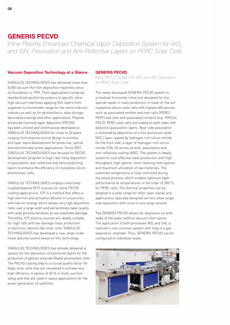
GENERIS PECVDInline PECVD System for AlO
x and SiN
y Deposition
on PERC Solar Cells
The newly developed GENERIS PECVD system is a modular horizontal inline tool designed for the special needs in mass production of state-of-the-art crystalline silicon solar cells with highest efficiencies, such as passivated emitter and rear cells (PERC/PERT) and cells with passivated contacts (e.g. TOPCon, POLO). PERC solar cells are coated on both sides with dielectric passivation layers. Rear side passivation is achieved by deposition of a thin aluminum oxide (AlOx) layer capped by hydrogen rich silicon nitride. On the front side, a layer of hydrogen rich silicon nitride (SiNx:H) serves as both, passivation and anti-reflective coating (ARC). The system is ideally suited for cost effective mass production with high throughput, high uptime, short cleaning interruptions and maximum utilization of raw materials. The substrate temperature is fully controlled during the whole process, which enables optimum layer performance at temperatures in the order of 350 °C for PERC cells. The thermal properties can be adapted in a wide range for other layer stacks and applications. Specially designed carriers allow single side deposition with close to zero wrap-around.
The GENERIS PECVD allows for deposition on both sides of the wafer without vacuum interruption. The application of both processes AlOx and SiNx is realized in one common system with help of a gas separation chamber. Thus, GENERIS PECVD can be configured to individual needs:

09
→ AlOx+SiNxontherearandSiNxonthefrontfor completepassivationofPERCandothercelltypes
→ AlOx+SiNxforPERCrearsideorn-PERTfront sidepassivation
→ SiNxonfrontand/orrearforanti-reflectiveor cappinglayeronly
→ SiOxorSiNxaspassivationand/ormaskinglayers forinterdigitatedbackcontactcells(IBC)and comparableapplications
→ Siliconandoraluminumbasedoxidicornitridic protectionorintermediatelayersfornextgeneration andtandemcellstructures
Especially the first configuration in which all PECVD layers are deposited in one tool represents a cost attractive, highly productive and straight forward production solution.
The system is using an inline process in which the substrates are transported on specially designed carriers for different wafer sizes. The carrier return system is located below the machine under clean environmental conditions. Different automation options for loading and unloading are available.
For the future, beyond the scope of silicon and aluminum based dielectric layers, GENERIS PECVD is already prepared for single-side deposition of doped amorphous and polycrystalline silicon layers for passivating contacts. High-rate inline deposition of these conductive semiconductor structures without wrap-around allows future industrial mass production of more advanced and ultra-high efficient cell architectures like TOPCon, POLO-BJ and tandem solar cells.
GENERIS PECVD – PERC Configurations

10
SILEX IIModular, Automated Wet Processing System for Batch Cleaning and Etching for Solar Cells
SILEX II Batch Wet Processing Equipment
TheSILEX II ALTEXmachineisdesignedtoapplyIPA-freetexturingprocesses,offeringsubstantialcostadvantagescomparedtotraditionaletchingsystems.Thistexturingprocesscanbeadjustedtotheindividualrequirementsofstandardandadvancedcelltechnologies.
TheSILEX II CLEANTEXcombinescommonetchingandcleaningstepsofmonocrystallineSiwithadvancedcleaningandconditioningprocesses.Efficientcleaningstepsareanindispensablerequirementtoimprovecellefficienciesandreduceoperationcosts.Ozone-basedcleaningoperations,appliedonSILEXIIwetbench,combineefficientorganicandmetalremovalwithanappropriatesurfaceconditioning.Duetolowchemicalcostsandconsumption,simpleprocesscontrolandhighmetalremovalefficiency,ozonized
SINGULUS TECHNOLOGIES provides complete automated dry-in/dry-out solutions for wet-chemical treatments of Si-wafers in standard and high-efficiency cell lines. The modular SILEX II batch system offers a wide range of process options. With respect to highest flexibility in configuration, the SILEX II machine is characterized by a clear modular design and a compact footprint. The SILEX II machine concept fulfills current and future requirements of capacity, flexibility and reliability for mass production.
The SILEX II 12000 was specially designed for larger production volumes. With this mass production system about 550 MW annual capacity are possible for Heterojunction cell manufacturing. The SILEX II 8000 system achieves an output of up to 8,000 wph. The SILEX II 4000 system with a reduced batch size will cover a tool capacity of up to 4,000 wph for smaller volume production. All SILEX II systems are running with very low scrap rates down to 0.01 % and a high process yield.
SILEX II
High Throughput Batch Wet Processing System for Heterojunction Cells with a Capacity of up to 8000 wph

11
Typical Features
→ Highthroughputperformanceupto550MW annualproduction
→ Highuptimeupto95%→ Lowbreakageratedownto0.01%→ Waferthicknessdownto120μm(wafersizeM6)
(‹120μmonrequest)→ Individual,flexibleprocesssequencing→ Onboardschedulersoftwareforthroughputtuning→ Onboardperformanceanalyzersoftware→ Ozone-enhancedcleaningandetchingprocesses→ ShortandstableIPA-freetexturingprocess→ Appropriateandeffectiverinsinganddrying
cleaningbathsaretheperfectsubstitutefortraditional,expensivemulti-stepRCAcleanings,knownfromthesolarandsemiconductorindustry.
TheSILEX II CLEANisprovidedtorundedicatedcleaningsequencesforpre-orpost-depositionprocesses.Dependingoncellprocessflowandrequirementtheconfigurationcanbedesignedindividually,involvingRCAorOzonebasedcleaningsaswellasslightetchingsteps.
Common and Advanced Process Applications
ETCHING
CLEANING
DRY
RINSE
→ Cascade Overflow → Dump-Spray System → Combination Rinse
→ Alkaline Texturing → Acidic Texturing → Chemical Polishing/Thinning → Metal and Oxide Etch
→ Hot/Cold Water Treatment → Hot Air, N2 Drying
→ Organic Cleaning → Metal Cleaning → Surface Conditioning

SubsidiariesOffices
←
2_01
6 -
5/20
21 S
tudi
o K
raus
e -
Pri
nted
in G
erm
any
- Te
chni
cal a
lter
atio
ns r
eser
ved
FranceSINGULUS TECHNOLOGIESFRANCE S.A.R.L.Tel. +33 3 8931 [email protected]
South AmericaSINGULUS TECHNOLOGIESLATIN AMERICA LTDA.Tel. +55 1121 [email protected]
Southeast AsiaSINGULUS TECHNOLOGIESASIA PACIFIC PTE LTD. Tel. +65 [email protected]
TaiwanSINGULUS TECHNOLOGIES TAIWAN LTD. Tel. +886 2 8692 6996 [email protected]
North AmericaSINGULUS TECHNOLOGIES INC. Tel. +1 860 683 [email protected]
Headquarters
SINGULUS TECHNOLOGIES AGHanauer Landstrasse 10363796 Kahl, GermanyTel. +49 6188 440-0Fax +49 6188 [email protected]
Production Site for Wet Processing Systems
SINGULUS TECHNOLOGIES AGBranch Office FuerstenfeldbruckFraunhoferstr. 982256 Fuerstenfeldbruck, GermanyTel. +49 8141 3600-0Fax +49 8141 [email protected]
Subsidiaries
ChinaSINGULUS TECHNOLOGIES (SHANGHAI) Co. Ltd.Room B412-413No. 1400 Jiangchang RoadJingan District, ShanghaiZip Code: 200072Tel. +86 21 [email protected]
SINGULUS TECHNOLOGIES Guangzhou OfficeRoom 539, 5F Block BNanlong Commercial CenterDalong No.31 Shilian Road, PanyuGuangzhou 511450Tel. +86 [email protected]
SINGULUS TECHNOLOGIES – Technologies for a Sustainable World
Responsible and sustainable corporate governance is very important to SINGULUS TECHNOLOGIES. SINGULUS TECHNOLOGIES develops and assembles innovative machines and systems for efficient and resource- saving production processes, which are used worldwide in the solar/ hydrogen, semiconductor, medical technology, consumer goods and data storage sectors. SINGULUS TECHNOLOGIES regards sustainability as an opportunity to position itself with innovative products that follow this spirit.In the focus are:
→ environmental awareness→ efficient use of resources→ avoidance of unnecessary CO2 pollution
The company's core competencies include various processes of coating technology, surface treatment and wet-chemical and thermal production processes.
THERMAL PROCESSING
WET CHEMICAL
SURFACE ENGINEERING
THIN FILM DEPOSITION