Embed Size (px)
Citation preview
Institute of Quantum Electronics
Nonlinear Optics LaboratoryAnnual Report 2003

February 2004
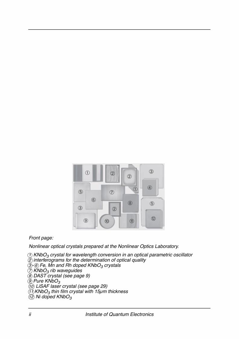
Front page:
Nonlinear optical crystals prepared at the Nonlinear Optics Laboratory.
1 KNbO3 crystal for wavelength conversion in an optical parametric oscillator2 interferograms for the determination of optical quality 3 - 6 Fe, Mn and Rh doped KNbO3 crystals7 KNbO3 rib waveguides8 DAST crystal (see page 9)9 Pure KNbO310 LiSAF laser crystal (see page 29)11 KNbO3 thin film crystal with 15µm thickness12 Ni doped KNbO3
�
�
�
� �
�
�
� ��
��
�
ii Institute of Quantum Electronics
Nonlinear OpticsLaboratory
Annual Report 2003
Prof. Dr. P. GünterNonlinear Optics LaboratoryInstitute of Quantum ElectronicsETH – Hönggerberg – HPFCH – 8093 Zürich
Phone: +41 1 633 2295Fax: +41 1 633 1056e-mail: [email protected]: http://www.nlo.ethz.ch/
Nonlinear Optics Laboratory iii
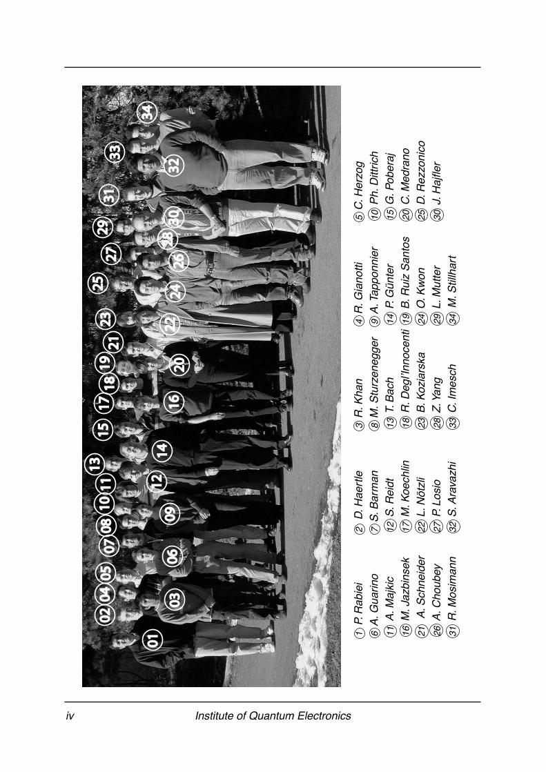
1 P
. Rab
iei
2 D
. Hae
rtle
3 R
. Kha
n4
R. G
iano
tti5
C. H
erzo
g6
A. G
uarin
o7
S. B
arm
an8
M. S
turz
eneg
ger
9 A
. Tap
ponn
ier
10 P
h. D
ittric
h11
A. M
ajki
c12
S. R
eidt
13 T
. Bac
h 14
P. G
ünte
r15
G. P
ober
aj16
M. J
azbi
nsek
17 M
. Koe
chlin
18 R
. Deg
l’Inn
ocen
ti19
B. R
uiz
San
tos
20 C
. Med
rano
21
A. S
chne
ider
22 L
. Nöt
zli
23 B
. Koz
iars
ka24
O. K
won
25 D
. Rez
zoni
co26
A. C
houb
ey27
P. L
osio
28 Z
. Yan
g29
L. M
utte
r30
J. H
ajfle
r31
R. M
osim
ann
32 S
. Ara
vazh
i33
C. I
mes
ch34
M. S
tillh
art
0707
0606
05050404 0303
0202
0101
1515
1414
1313
121211111010
0909
08082525
2424
2323 2222
2121
202019191818
1717 1616
2929
30302828
2727 2626
3131
3232
3333
3434
iv Institute of Quantum Electronics
Mem
ber
s o
f th
e N
on
linea
r O
pti
cs L
abo
rato
ry 2
003
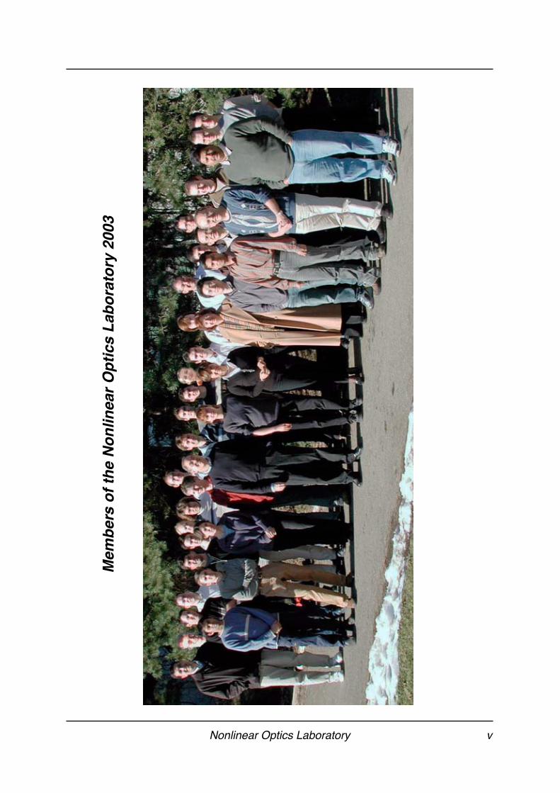
Nonlinear Optics Laboratory v

vi Institute of Quantum Electronics
PERSONNEL 3
ACADEMIC AND CORPORATE VISITORS 4
SPONSORS 4
RESEARCH SUMMARY 5Activities of members of the Nonlinear Optics Laboratory in
Conference Committees and Editorial Boards 6Teaching 7
INTEGRATED OPTICS AND MICRORESONATORS 9Organic Electro-optic Crystals and Thin Films 9Electro Optic Polymers 10Organic Electro-optic Microcavities 11Thin Films of LiNbO3 for Integrated Optics Applications Prepared by Smart Cut Method 12Highly Integrated Electro-optical Devices Based on
K1-yNayTa1-xNbxO3 and KNbO3 crystals 13Characterization of Nonlinear Optical Materials 14Femtosecond Laser Structuring of DAST 15
PHOTOREFRACTIVE OPTICS 17Growth, Preparation and Characterization of Photorefractive Crystals 17Deep Ultraviolet Interband Photorefraction and Dynamic Waveguides in Lithium Tantalate 18Holographic Optical Elements for Infrared Lasers 19Optical and Nonlinear Optical Properties of Sn2P2S6 Crystals 20Layered Photorefractive Polymers 21
PHOTONIC MATERIALS TECHNOLOGIES 23Supramolecular Organic Thin Films for Nonlinear Optics 23Optical and Electrical Properties of Amorphous Organic
Semiconductors under Intense Electrical Excitation 24Charge Injection and Transport in Amorphous Organic Semiconductors 25Generation and detection of THz pulses 26Femtosecond Nonlinear Spectroscopy 27
BLUE AND UV SOLID STATE LASERS 29Frequency Doubled Diode Pumped Solid-State Lasers 29Compact Blue Light Sources Using KNbO3 Waveguides 30Compact Blue Light Sources Using KNbO3 and Cr:LiSAF Waveguides 31UV Solid State Waveguide Lasers 32
PUBLICATIONS 2003 33
PRESENTATIONS 2003 36
PHD THESES IN PHYSICS 2003 39
DIPLOMA THESES IN PHYSICS 2003 40
Nonlinear Optics Laboratory 1

2 Institute of Quantum Electronics
PERSONNEL
PERSONNEL
HeadProf. Dr. P. Günter
Academic GuestsProf. Dr. Roger Cudney CICESE, Ensenada, MexicoDr. Alexandar A. Grabar Uzhgorod State University, UkraineProf. Dr. Igor Poberaj Institute Jozef Stefan, Ljubljana, SIProf. Dr. Marko Zgonik Institute Jozef Stefan, Ljubljana, S
Project LeadersDr. Mojca Jazbinsek since August
Dr. Carolina MedranoPD Dr. Germano MontemezzaniPaolo LosioProf. Dr. Marko Zgonik until July
Academic StaffDr. Shanmugam Aravazhi Dr. O-Pil Kwon since September
Tobias Bach since April Dr. Pierre LavéantDr. Ashutosh Choubey Aleksej MajkicRiccardo Degl’Innocenti Lukas MutterPhilipp Dittrich Dr. Payam Rabiei since March
Andrea Guarino Dr. Ali RashidDaniel Haertle Daniele RezzonicoChristian Herzog Blanca RuizDr. Mojca Jazbinsek until July Arno SchneiderDr. Rizwan Khan since November Axelle TapponnierDr. Bozena Koziarska-Glinka Dr. Zhou Yang since October
Electronic and Laser EngineersSacha Barman Steffen Reidt since May
Technical StaffReto Gianotti Hermann Wüest until May
Jaroslav Hajfler
Administrative StaffLiselotte Artel Lotti Nötzli
Nonlinear Optics Laboratory 3
ACADEMIC AND CORPORATE VISITORS
ACADEMIC AND CORPORATE VISITORSTobias Bach TU, München, DDr. Pietro Bernasconi Lucent Technologies, Holmdel, USADr. Lukas Bürgi Cavendish Laboratory, Cambridge, UKDr. Mart Diemeer Technical University Twente, NLDr. Hans-Jürgen Eisler Universität Karlsruhe, DDr. Holger Frohne Universität Köln, DDr. Paul Golding Giga Tera Inc., DietikonDr. Alexandar A. Grabar University of Uzhgorod, UkraineDr. Gilles Guerrero EPFL LausanneDr. Jean-Pierre Huignard Thales-Group, Orsay, FDr. Rizwan Khan Imperial College, London, UKLars Lundeberg Chalmers University, Göteborg, SDr. Gorazd Poberaj DLR (German Aerospace Center),
Oberpfaffenhofen, DProf. Dr. Igor Poberaj Institute Jozef Stefan, Ljubljana, SIDr. Shiro Shichijyo Mitsui Chemicals, JapanDr. Takao Takahashi Mitsui Chemicals, JapanDr. Kimberly Willis University of Sheffield, UK
SPONSORSETH ZürichSwiss National Science FoundationNational Research Program NFP 47“Supramolecular Functional Materials”KTIEU-Research Program ISTBBW
4 Institute of Quantum Electronics
RESEARCH SUMMARY
RESEARCH SUMMARYThis report summarizes the main research activities performed within the
Nonlinear Optics Laboratory in 2003. Our group was active in the following fields:
• Integrated Optics and Microresonators
• Photorefractive Optics
• Photonics Materials Technology
• Blue and UV Solid State Lasers
The research projects in these areas are described briefly in this report. One of the
main newer research areas is the EU funded project on:
"Next Generation Active Integrated Optic Subsystems (NAIS)"
and related research on inorganic and organic active microresonators.
For more details I refer to the different contributions in this report and our WEB
page: http://www.nlo.ethz.ch/
In 2003 our technical assistant and long time crystal growth expert
Hermann Wüest has accepted an administrative position in the Physics Department
and has left the Nonlinear Optics Laboratory. During this year we could welcome
Dr. Rizwan Khan, Dr. O-Pil Kwon, Dr. Payam Rabiei and Dr. Zhou Yang as new
postdoctoral fellows, Tobias Bach as assistant and PhD student and Steffen Reidt as
laser engineer.
It is my pleasure to thank all scientific, technical and administrative group mem-
bers for their active collaboration and the ETH, the Swiss National Science Foun-
dation, the KTI and other external funding organisations for their financial support.
Nonlinear Optics Laboratory 5
RESEARCH SUMMARY
Activities of members of the Nonlinear Optics Laboratory in Conference Committees and Editorial Boards 0.1
Several members of the nonlinear optics laboratory continued to be active in a se-ries of international committees and as editorial board member of scientific journalsin the fields of optics, nonlinear optics, quantum electronics, solid state physics offerroelectric, organic and polymeric materials. Prof. P. Günter is a member of theeditorial board of the following scientific journals:
• "Ferroelectrics"• "Ferroelectrics Letters"• "Nonlinear Optics"• "Optics Communication"• "Photonics Science News"
and is a member of the advisory or program committees of the following interna-tional conferences:
• "European Conference on Applications of Polar Dielectrics" (ECAPD)(Chairman of the European Steering Committee)
• IEEE Ferroelectrics Committee of the "Ultrasonics, Ferroelectrics and Fre-quency Control Society"
• "International Conference on Organic Nonlinear Optics" (ICONO-7) • "European Conference on Lasers and Electro-optics" (CLEO/Europe 2003)
(Program Committee)• "OSA topical meeting on "Photorefractive Materials and Applications"• "Nonlinear Optics 2004" (OSA Topical Conference) (Program Committee) • "European Meeting on Ferroelectricity"• "International Workshop on Photonic Materials for the New Century"• "International Conference on Photoactive Organics and Polymers"• "International Workshop on Organic Self-Assembly"• "International Conference on Organic and Molecular Electronics and Photo-
nics"
Zürich, February 2004 Prof. Peter Günter
6 Institute of Quantum Electronics
RESEARCH SUMMARY
Teaching 0.2
P. Günter"Physics II" for electrical engineersWS 2002/2003
P. Günter"Physics I" for civil, environmental and geomatical engineersWS 2003/2004
G. Montemezzani"Holographie und optische Phasenkonjugation"WS 2002/2003
G. Montemezzani"Electro-optics"SS 2003
G. Montemezzani"Holographie und optische Phasenkonjugation"WS 2003/2004
Ch. Bosshard (CSEM Alpnach)"Nonlinear Optics"WS 02/03
Ch. Bosshard (CSEM Alpnach)"Nonlinear optical spectroscopy: fundamentals and applications"SS 03
Ch. Bosshard (CSEM Alpnach)"Nonlinear Optics"WS 03/04
Nonlinear Optics Laboratory 7

8 Institute of Quantum Electronics
INTEGRATED OPTICS AND MICRORESONATORS
INTEGRATED OPTICS AND MICRORESONATORSOrganic Electro-optic Crystals and Thin Films 1.1
P. Lavéant, B. Ruiz, R. Gianotti and J. Hajfler
Aims: We investigate different methods to produce organic electro optic crystals.Although the major aim is to grow DAST single crystals, the design and synthesisof new materials with even larger non-linear optical properties is also pursued. Theprocessing of the resulting crystals such as cutting, polishing and protection shouldalso be optimized.
Approach: DAST (4-N,N-dimethylamino-4’-N’-methyl stilbazolium tosylate)crystal is very atractive for several applications and especially for integrated elec-tro-optic modulators due to relatively high electro-optic coefficients and low dielec-tric constants. Bulk crystal growth is achieved within a seeded and saturatedsolution with precisely controlled temperature ramp. For integrated optics applica-tions the possibility of producing a thin film of single crystalline organic materialis extremely attractive. Therefore we study methods for producing thin single crys-tals of DAST on various substrates. Exploratory methods are applied to the newmaterials currently being sinthetized to produce crystals and study their propertieson the bulk.
Results: 16 growth cells work in parallel to grow bulk crystals from the solution.DAST crystals with sizes of 1 to 3 cm3 are now routinely produced. The large num-ber of cells working in parallel allows an intensive search of the optimal growth pa-rameters and a better understanding of the growth mechanisms of organic salts.Thin single crystals are also obtained with a typical size of 1 mm2 for a thickness of100 microns. The control of the nucleation and the influence of the substrate arecritical issues, which are now intensively investigated. A new polishing method thatallows us to obtain surface roughnesses of less than 10 nm has been developed. Anadecuate protection material has been identified for our organic crystals. Addition-ally to DAST growth, the first JH (trans-4-dimethylamino-N-R-silbazoliumhexafluorophosphate) crystals, that show similar powder SHG activity as DAST,were grown this year in collaboration with the University of Manchester.
DAST crystal polished along thedielectric axes.
Reference: P. Lavéant, C. Medrano,B. Ruiz and P. Günter,
Growth of Nonlinear Optical DASTCrystals,
Chimia 57 (6), 349-351 (2003)
Nonlinear Optics Laboratory 9
INTEGRATED OPTICS AND MICRORESONATORS
Electro Optic Polymers 1.2
D. Rezzonico, O.-P. Kwon and M. Jazbinsek
Aims: Production of waveguide structures in forms of passive microcavity resona-tors with materials, which would later allow upgrading to active microresonators.The device based on such microresonators should work in the telecommunicationwavelength range from 1500 to 1600 nm.
Approach: Organic molecules and polymers combine the nonlinear optical prop-erties of conjugated π-electron systems with the possibility of additional molecularengineering, i.e. creating new materials with appropriate optical, structural, and me-chanical properties.We aim to apply existing as well as new polymers to electro-optic modulators. Therelatively simple methods of producing polymer waveguides are very attractive forproducing advanced microcavity resonators. The most demanding skill is to obtaina high aspect ratio of the produced channel waveguides. We are developing andsynthesing electro-optic materials in collaboration with synthetic chemists withinand outside of our research group.
Results: After the demonstration of the filtering features of microrings of the poly-meric resin Cyclotene (TM of Dow Chemicals) our target was to search for im-proved patterning techniques and polymeric materials in order to get higherresonator finesses. A series of different glues and resins was tested. We identifiedthe hybrido-polymer ORMOCER (TM of Fraunhofer Institut, Wuerzburg, Germa-ny) among the most suitable polymers for channel waveguide’s structuring. This or-ganic modified silicate has the advantage to be patterned directly after UV exposurewithout agressive etching processes so that the edges of the resulted channels are ofhigh quality. We also started the synthesis of new electro-optically active polymers.Next step is to investigate the way of combining the good structurable passive ma-terials together with the active compounds.
Section view of fourwaveguides in Ormocer (Or-mocore) surrounded by alow index type of the samematerial (Ormoclad). Thestructures were pruduced onoxidized silicon wafers.
10 µm
10 Institute of Quantum Electronics
INTEGRATED OPTICS AND MICRORESONATORS
Organic Electro-optic Microcavities 1.3
B. Koziarska-Glinka, C. Herzog and M. Zgonik
Aims: Investigate the properties of new passive integrated optic structures in com-bination with active electro-optic materials for use in compact electro-optical ele-ments for fiber telecommunications. Using hybrid integration of passive and activematerials a working prototype of microresonator-based mux/demux and high-speedswitch and modulator should be demonstrated.
Aims: Straight waveguide segments made out of Si3N4 form the input and outputports. By means of evanescent field coupling the waveguides interact with the TiO2or SOI micro resonator. The cavity causes a narrow-bandwidth, frequency depen-dent transfer of power between the port waveguides. Metallic electrodes are includ-ed to create an electric field in the active DAST overlay, thereby changing theresonance condition of the ring resonator.
Results: In a first attempt, DAST is applied as an electro-optic top cladding on pas-sive straight waveguides with parallel electrodes. In order to obtain a sufficientlyhigh effective index of composite waveguides and to exceed the index of DAST,Si3N4 as well as TiO2 core layers are studied.Using numerical calculations the critical design parameters and material propertiesfor efficient coupling and low loss mode propagation have been identified.In a preliminary experiment the first modulation measurements have been per-formed in a straight waveguide and an external interferometer.
A scheme of an electro optic active microring resonator verticallycoupled to two straight optical waveguides.
Nonlinear Optics Laboratory 11
INTEGRATED OPTICS AND MICRORESONATORS
Thin Films of LiNbO3 for Integrated Optics Applications Prepared by Smart Cut Method 1.4
P. Rabiei
Aims: Fabrication of thin films of LiNbO3 using smart cut method. Thin films ofLiNbO3 with bulk quality are required for the integrated optical devices. In thisproject the fabrication using smart cut method is investigated. Thin films with submicro-meter thickness are produced on low refractive index cladding layer.
Approach: A LiNbO3 crystal is ion implanted using ionized He+ atoms. A layer ofSiO2 is deposited on another LiNbO3 sample using plasma enhanced chemical va-por deposition system. This layer will behave as a buffer layer or a cladding for theoptical waveguide, which will be fabricated. A thin film polishing technique is de-veloped to smoothen the surface of the deposited SiO2 layer. The ion implantedsample and the sample with cladding layer are bonded together using standard wa-fer bonding techniques. The samples are brought into contact inside de-ionized wa-ter and are pressed against each other to form a bond between them. The sampleswill attach to each other after this process. Next the bonded samples are heat treatedto increase the bonding strength. By increasing the temperature further to 600ºC, athin layer of crystal is split and transferred to another substrate. Hence one will ob-tain a thin layer of the nonlinear crystal using this method.
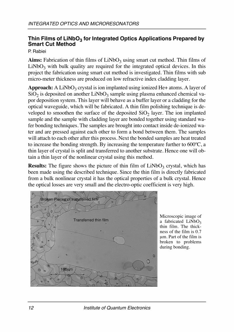
Results: The figure shows the picture of thin film of LiNbO3 crystal, which hasbeen made using the described technique. Since the thin film is directly fabricatedfrom a bulk nonlinear crystal it has the optical properties of a bulk crystal. Hencethe optical losses are very small and the electro-optic coefficient is very high.
Microscopic image ofa fabricated LiNbO3thin film. The thick-ness of the film is 0.7µm. Part of the film isbroken to problemsduring bonding.
12 Institute of Quantum Electronics
INTEGRATED OPTICS AND MICRORESONATORS
Highly Integrated Electro-optical Devices Based on K1-yNayTa1-xNbxO3 and KNbO3 crystals 1.5
S. Aravazhi and A. Guarino
Aims: Preparation of waveguiding thin films for integrated optics and exploit theoutstanding pyroelectric, electro-optic and nonlinear optic properties of the solid so-lution system K1-yNayTa1-xNbxO3 (KNTN).
Approach: Growth of KNTN thin films on (100) oriented KTaO3 substrates byliquid phase epitaxy. In order to increase the conductivity of the substrates, KTaO3doped with Ba is grown by the top seeded solution growth method. The substrateobtained in this way can be used as a bottom electrode in pyroelectric and electro-optic applications requiring an out of plane electric field direction. By varying the ratio of K/Na atoms in the KNTN films the lattice matching of thefilm - in the cubic phase - with the substrate can be adjusted to better than 0.03%.Poling of the film is possible over small areas in the in-plane or out-of-plane direc-tion. Properties of films with the thickness of 1-10µm are studied with respect totheir optical and nonlinear optic properties.
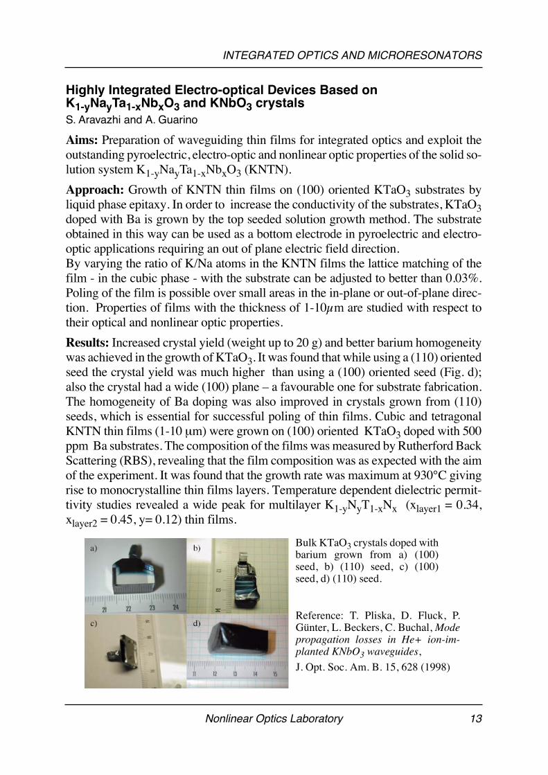
Results: Increased crystal yield (weight up to 20 g) and better barium homogeneitywas achieved in the growth of KTaO3. It was found that while using a (110) orientedseed the crystal yield was much higher than using a (100) oriented seed (Fig. d);also the crystal had a wide (100) plane – a favourable one for substrate fabrication.The homogeneity of Ba doping was also improved in crystals grown from (110)seeds, which is essential for successful poling of thin films. Cubic and tetragonalKNTN thin films (1-10 µm) were grown on (100) oriented KTaO3 doped with 500ppm Ba substrates. The composition of the films was measured by Rutherford BackScattering (RBS), revealing that the film composition was as expected with the aimof the experiment. It was found that the growth rate was maximum at 930°C givingrise to monocrystalline thin films layers. Temperature dependent dielectric permit-tivity studies revealed a wide peak for multilayer K1-yNyT1-xNx (xlayer1 = 0.34,xlayer2 = 0.45, y= 0.12) thin films.
Bulk KTaO3 crystals doped withbarium grown from a) (100)seed, b) (110) seed, c) (100)seed, d) (110) seed.
Reference: T. Pliska, D. Fluck, P.Günter, L. Beckers, C. Buchal, Modepropagation losses in He+ ion-im-planted KNbO3 waveguides,
J. Opt. Soc. Am. B. 15, 628 (1998)
Nonlinear Optics Laboratory 13
INTEGRATED OPTICS AND MICRORESONATORS
Characterization of Nonlinear Optical Materials 1.6
L. Mutter, Z. Yang, O.-P. Kwon and M. Jazbinsek
Aims: For electronic and photonic applications organic molecules with extendedconjugation of the π-orbitals and donor-acceptor end groups are of particular inter-est. We look for new materials and characterize them with respect to their electrical,linear optical and nonlinear optical properties. We are also interested in their tem-perature stability and optical damage resistance.
Approach: Investigation of new molecules with electric field induced second har-monic generation (EFISH) and hyper-Rayleigh scattering. Wavelength dependenttransmission/reflection measurements, Michelson interferometric measurementsand Maker fringe second harmonic generation are used to determine the linear op-tical properties, transparency range and second-order nonlinear optic properties ofnew materials. Electro-optic measurements are used to characterize new materialsfor applications in high frequency modulators, detectors and sources of THz elec-tromagnetic waves. Pulsed degenerate four wave mixing and third harmonic gen-eration are used to characterize third order nonlinear optical susceptibilities of newmaterials.
Results: Encouraged by the excellent nonlinear optical properties of DAST, neworganic nonlinear crystals based on strong Coulomb interaction to induce highlynoncentrosymmetric and stable packing are being developed. Second harmonicgeneration (SHG) was studied in a series of new crystal powders as a preliminarytest of their bulk NLO activities. The results show that some of them have pro-nounced SHG activities similar to that of DAST. Single crystal X-ray crystallo-graphic studies are in progress to get details about their crystal structures.
Reference: L. Mutter, M. Jazbinsek, M. Zgonik, U. Meier, Ch. Bosshard and P. Günter, Pho-tobleaching and optical properties of DAST, J. Appl. Phys. 94, 1356 (2003)
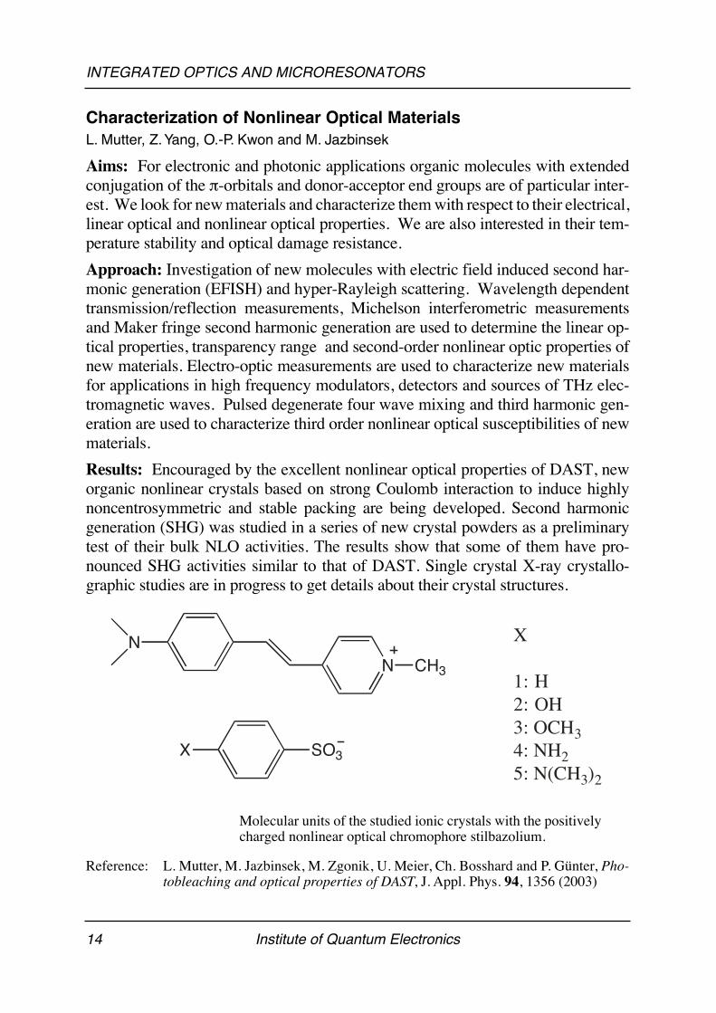
Molecular units of the studied ionic crystals with the positivelycharged nonlinear optical chromophore stilbazolium.
NN CH3
SO3X
X
1: H2: OH3: OCH34: NH25: N(CH3)2
14 Institute of Quantum Electronics
INTEGRATED OPTICS AND MICRORESONATORS
Femtosecond Laser Structuring of DAST 1.7
A. Guarino, L. Mutter and Ph. Dittrich
Aims: We investigate the method of femtosecond laser ablation regarding its appli-cability for the structuring of electro-optical crystals. After promising preliminaryresults on the fabrication of waveguides on the surface of 4-N, N-dimethylamino-4’-N’-methyl-stilbazolium tosylate (DAST), we pursue the improvement of thequality of the ablated structures and the decrease of their size to achieve a resolutionsuitable for integrated optics applications. Beside DAST also structuring of inor-ganic materials like KNbO3 are of primary interest.
Approach: Femtosecond (fs) laser ablation has indeed many advantages with re-spect to damage free material processing. By focusing femtosecond pulses on thesurface of a material, it can be ablated and structured very effectively without de-stroying neighboring or underlying regions due to the short interaction time inwhich essentially no energy can be transferred to the crystal lattice. This is especial-ly interesting in the case of waveguide fabrication using nonlinear optical materials,where the crystalline structure inside the waveguide should be maintained.
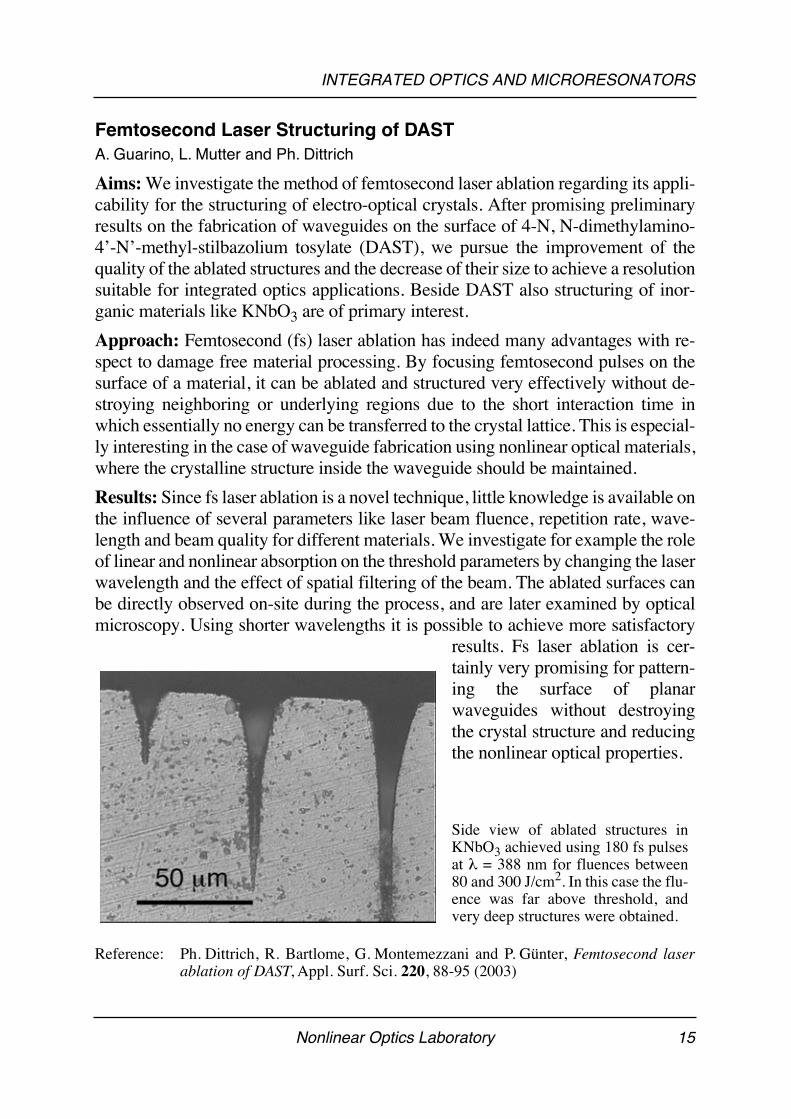
Results: Since fs laser ablation is a novel technique, little knowledge is available onthe influence of several parameters like laser beam fluence, repetition rate, wave-length and beam quality for different materials. We investigate for example the roleof linear and nonlinear absorption on the threshold parameters by changing the laserwavelength and the effect of spatial filtering of the beam. The ablated surfaces canbe directly observed on-site during the process, and are later examined by opticalmicroscopy. Using shorter wavelengths it is possible to achieve more satisfactory
results. Fs laser ablation is cer-tainly very promising for pattern-ing the surface of planarwaveguides without destroyingthe crystal structure and reducingthe nonlinear optical properties.
Reference: Ph. Dittrich, R. Bartlome, G. Montemezzani and P. Günter, Femtosecond laserablation of DAST, Appl. Surf. Sci. 220, 88-95 (2003)
Side view of ablated structures inKNbO3 achieved using 180 fs pulsesat λ = 388 nm for fluences between80 and 300 J/cm2. In this case the flu-ence was far above threshold, andvery deep structures were obtained.
Nonlinear Optics Laboratory 15

INTEGRATED OPTICS AND MICRORESONATORS
16 Institute of Quantum Electronics
PHOTOREFRACTIVE OPTICS
PHOTOREFRACTIVE OPTICSGrowth, Preparation and Characterization of Photorefractive Crystals 2.1
A. Choubey, H. Wüest, J. Hajfler, M. Jazbinsek and D. Haertle
Aims: This project is aimed at the investigation and characterization of several in-organic photorefractive materials (KNbO3, Sn2P2S6, LiTaO3) and the assessmentof their performance in view of different applications involving ultraviolet, visibleor near infrared light.
Approach: Crystals of KNbO3 are grown in our laboratory by the top seeded solu-tion growth method. This year we have concentrated on the growth of pure and Rhdoped crystals with seed direction [010]c (or b direction) rather than the convention-al seeds of [101]c direction. Other materials under investigation are stoichiometricLiTaO3 crystals grown at the National Institute for Materials Science in Tsukuba,Japan (Dr. K. Kitamura) by a double crucible method, as well as Sn2P2S6 crystalsand derivatives grown at the University of Uzhgorod, Ukraine in the group of Prof.Y. Vysochanskii and Dr. A. A. Grabar. A furnace with two separate heating zonesfor the growth of this crystal by the chemical vapour transport method was also con-structed at ETH. The crystal quality and performance of all materials are character-ized by various physical, optical and photorefractive methods, such as absorptionand photoconduction spectroscopy and photorefractive wave mixing.
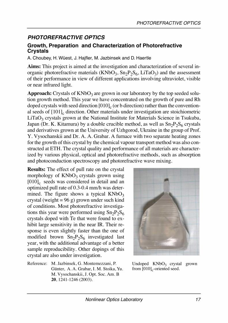
Results: The effect of pull rate on the crystalmorphology of KNbO3 crystals grown using[010]c seeds was considered in detail and anoptimized pull rate of 0.3-0.4 mm/h was deter-mined. The figure shows a typical KNbO3crystal (weight = 96 g) grown under such kindof conditions. Most photorefractive investiga-tions this year were performed using Sn2P2S6crystals doped with Te that were found to ex-hibit large sensitivity in the near IR. Their re-sponse is even slightly faster than the one ofmodified brown Sn2P2S6 investigated lastyear, with the additional advantage of a bettersample reproducibility. Other dopings of thiscrystal are also under investigation.
Reference: M. Jazbinsek, G. Montemezzani, P. Günter, A. A. Grabar, I. M. Stoika, Yu. M. Vysochanskii, J. Opt. Soc. Am. B 20, 1241-1246 (2003).
Undoped KNbO3 crystal grownfrom [010]c-oriented seed.
Nonlinear Optics Laboratory 17
PHOTOREFRACTIVE OPTICS
Deep Ultraviolet Interband Photorefraction and Dynamic Waveguides in Lithium Tantalate 2.2
Ph. Dittrich, B. Koziarska-Glinka and G. Montemezzani
Aims: Major advantages of interband photorefraction, compared with the conven-tional photorefractive effect, are faster response times and a greater robustness ofthe induced gratings with respect to sub-bandgap illumination. The aim of thisproject is to investigate deep ultraviolet (UV) interband photorefraction in pure andmagnesium doped near stoichiometric lithium tantalate, promising materials forshort-wavelength holographic data storage and dynamic holography. One furtheraim is to demonstrate light induced, dynamic waveguides in LiTaO3.
Approach: Near stoichiometric LiTaO3 crystals have been investigated by Braggdiffraction experiments. Special attention was given to the influence of stoichiom-etry and doping. Using interband photorefraction and via the linear electrooptic ef-fect, we also expect to be able to induce dynamic waveguides underneath thesurface of a LiTaO3 crystal by the spatial distribution of a top surface UV illumi-nation. By modifying the surface illumination of the crystal the waveguide struc-tures should be controllable and be reconfigurable in real time.
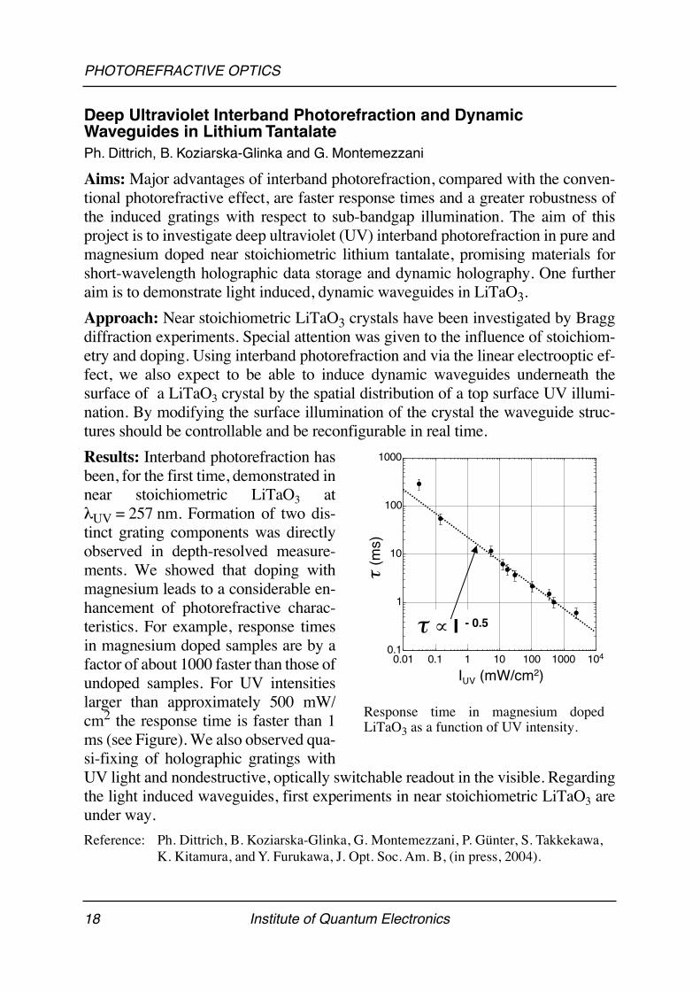
Results: Interband photorefraction hasbeen, for the first time, demonstrated innear stoichiometric LiTaO3 atλUV = 257 nm. Formation of two dis-tinct grating components was directlyobserved in depth-resolved measure-ments. We showed that doping withmagnesium leads to a considerable en-hancement of photorefractive charac-teristics. For example, response timesin magnesium doped samples are by afactor of about 1000 faster than those ofundoped samples. For UV intensitieslarger than approximately 500 mW/cm2 the response time is faster than 1ms (see Figure). We also observed qua-si-fixing of holographic gratings withUV light and nondestructive, optically switchable readout in the visible. Regardingthe light induced waveguides, first experiments in near stoichiometric LiTaO3 areunder way.
Reference: Ph. Dittrich, B. Koziarska-Glinka, G. Montemezzani, P. Günter, S. Takkekawa, K. Kitamura, and Y. Furukawa, J. Opt. Soc. Am. B, (in press, 2004).
Response time in magnesium dopedLiTaO3 as a function of UV intensity.
IUV (mW/cm2)0.01 0.1 1 10 100 1000 104
0.1
1
10
100
1000
τ (m
s)
τ ∝ I - 0.5
18 Institute of Quantum Electronics
PHOTOREFRACTIVE OPTICS
Holographic Optical Elements for Infrared Lasers 2.3
T. Bach, M. Jazbinsek and G. Montemezzani
Aims: Compared to other high power cw sources, laser diodes and laser diode ar-rays are compact, efficient and cheap. The main disadvantages are a reduced spatialbeam quality and a rather broad spectral distribution. The aim of this work is to im-prove the spatial and spectral properties of near infrared laser diodes and laser diodearrays by means of holographic techniques. This would be attractive for a largenumber of applications, such as longitudinal pumping, frequency conversion, or la-ser printing or machining.
Approach: Two different approaches are being considered, which involve eitherstatic or dynamic holograms. Static holograms are mainly useful for spatial reshap-ing of the laser diode beam. Complex holographic optical elements in combinationwith an external grating or a second hologram can be used for an additional frequen-cy locking of the emitted light. Due to the large dynamic range, our materials ofchoice here are different types of photopolymers. The second appoach involves dy-namic holograms recorded in infrared sensitive photorefractive media. Upon care-ful design of the set-up, the combined nonlinear dynamics in the laser medium andthe external dynamic holograms should lead the system to self-organize into a statewith a nearly diffraction limited output and a much narrower spectral bandwidth.
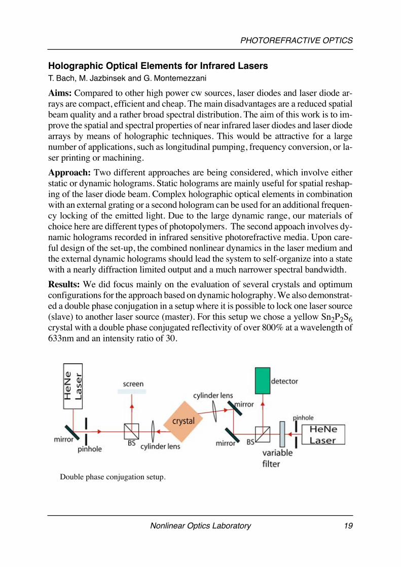
Results: We did focus mainly on the evaluation of several crystals and optimumconfigurations for the approach based on dynamic holography. We also demonstrat-ed a double phase conjugation in a setup where it is possible to lock one laser source(slave) to another laser source (master). For this setup we chose a yellow Sn2P2S6crystal with a double phase conjugated reflectivity of over 800% at a wavelength of633nm and an intensity ratio of 30.
Double phase conjugation setup.
Nonlinear Optics Laboratory 19
PHOTOREFRACTIVE OPTICS
Optical and Nonlinear Optical Properties of Sn2P2S6 Crystals 2.4
D. Haertle and G. Montemezzani
Aims: Sn2P2S6 has recently established itself as a very promising crystal for appli-cations involving photorefraction or nonlinear optics. However, several of the basicmaterial properties of this low symmetry crystal are still unknown. The aim of thepresent project is to partially close this gap by performing direct measurements forthe determination of the dielectric, electro-optical and nonlinear optical tensor com-ponents of this material.
Approach: After having measured the most important electro-optical coefficientslast year, we turn our attention to the refractive indices and the nonlinear optical ten-sor. In Sn2P2S6 the refractive indices are fully determined by measuring its mainvalues , and as well as the orientation of the dielectric axes with respect tothe crystallographic axes. The main refractive indices were measured with a mini-mum-deviation setup. The rotation of the dielectric axes was determined by findingthe eigenpolarizations at different wavelengths and temperatures.The precise knowledge of the refractive indices permits to predict the best configu-rations for nonlinear optics. Nonlinear optical coefficients were measured by theMaker-fringe experiment.
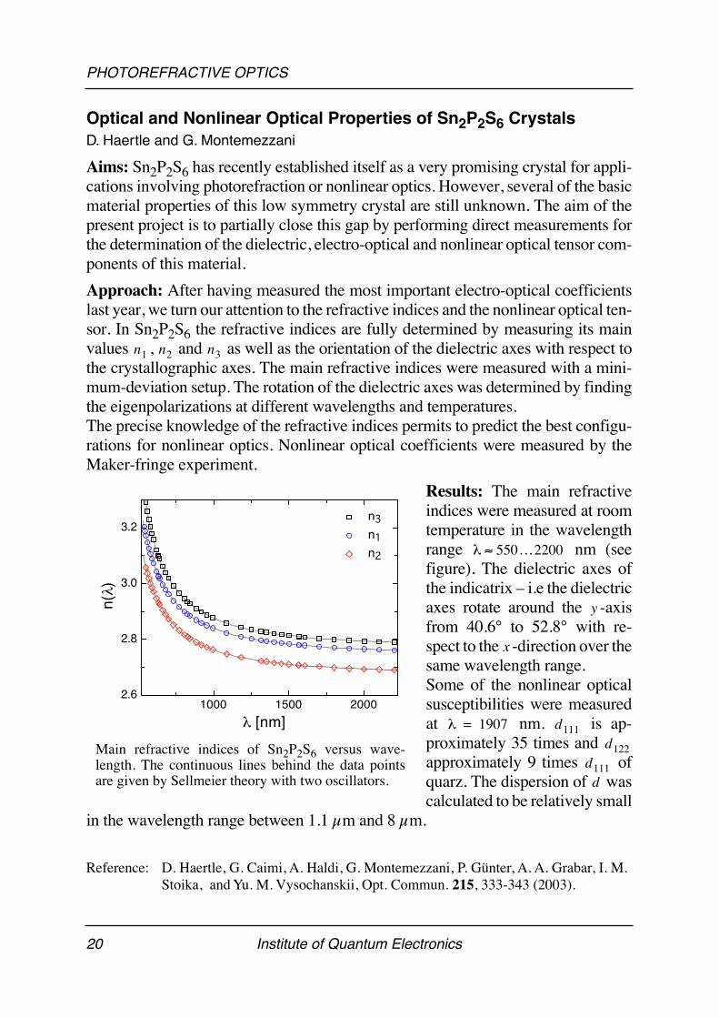
Results: The main refractiveindices were measured at roomtemperature in the wavelengthrange nm (seefigure). The dielectric axes ofthe indicatrix – i.e the dielectricaxes rotate around the -axisfrom 40.6° to 52.8° with re-spect to the -direction over thesame wavelength range.Some of the nonlinear opticalsusceptibilities were measuredat nm. is ap-proximately 35 times and approximately 9 times ofquarz. The dispersion of wascalculated to be relatively small
in the wavelength range between 1.1 µm and 8 µm.
Reference: D. Haertle, G. Caimi, A. Haldi, G. Montemezzani, P. Günter, A. A. Grabar, I. M.
Stoika, and Yu. M. Vysochanskii, Opt. Commun. 215, 333-343 (2003).
n1 n2 n3
Main refractive indices of Sn2P2S6 versus wave-length. The continuous lines behind the data pointsare given by Sellmeier theory with two oscillators.
1000 1500 20002.6
2.8
3.0
3.2
λ [nm]
n(λ)
n3n1n2 λ 550…2200≈
y
x
λ 1907= d111d122
d111d
20 Institute of Quantum Electronics
PHOTOREFRACTIVE OPTICS
Layered Photorefractive Polymers 2.5
O.-P.- Kwon and G. Montemezzani
Aims: Polymer composites showing a charge transport mediated photorefractiveeffect hold promise for efficient and cheap dynamic holographic devices for opticalprocessing. In this project, in collaboration with the Ajou University (Korea), we in-vestigate a novel very promising class of photorefractive composites that spontane-ously form a layered structure and show low glass transition temperatures inabsence of a plasticizer, without sacrifying the stability.
Approach: The materials studied in thiswork are based on a rigid backbonewhich is composed by poly(p- phe-nylene terephthalate) (PPT). A chargetransporting carbazole group (CZ) isconnected to the polymer backbone byoxyalkyl spacers of variable length. Sev-eral such composites containing C60 as asensitizer and diethylaminodicyanosty-rene (DDCST) or piperidinodicyanosty-rene (PDCST) as nonlinear opticalchromophores are prepared. The investi-gations involve x-ray and thermal char-acterization, dielectric, electro-optic andphotoconduction studies, as well as thephotorefractive characterization by two-wave mixing and Bragg diffraction.
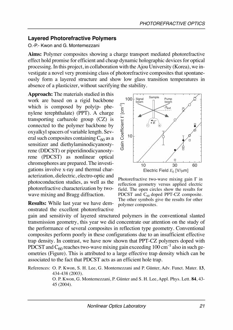
Results: While last year we have dem-onstrated the excellent photorefractivegain and sensitivity of layered structured polymers in the conventional slantedtransmission geometry, this year we did concentrate our attention on the study ofthe performance of several composites in reflection type geometry. Conventionalcomposites perform poorly in these configurations due to an insufficient effectivetrap density. In contrast, we have now shown that PPT-CZ polymers doped withPDCST and C60 reaches two-wave mixing gain exceeding 100 cm-1 also in such ge-ometries (Figure). This is attributed to a large effective trap density which can beassociated to the fact that PDCST acts as an efficient hole trap.
References: O. P. Kwon, S. H. Lee, G. Montemezzani and P. Günter, Adv. Funct. Mater. 13,434-438 (2003).O. P. Kwon, G. Montemezzani, P. Günter and S. H. Lee, Appl. Phys. Lett. 84, 43-45 (2004).
Photorefractive two-wave mixing gain Γ inreflection geometry versus applied electricfield. The open circles show the results forPDCST and C60 doped PPT-CZ composite.The other symbols give the results for otherpolymer composites.
10 30 60
10
100
Electric Field E0 [V/µm]
Gai
n C
oeffi
cien
t Γ [c
m-1
]+–
+ E
θext
SampleSignalbeam
Pumpbeam
Nonlinear Optics Laboratory 21
PHOTOREFRACTIVE OPTICS
22 Institute of Quantum Electronics
PHOTONIC MATERIALS TECHNOLOGIES
PHOTONIC MATERIALS TECHNOLOGIESSupramolecular Organic Thin Films for Nonlinear Optics 3.1
A. Rashid
Aims: To develop a simple and effective method for the supramolecular self-as-sembling of thin films with directional ordering perpendicular to the surface of thesubstrate. The essential criteria are: (1) improved growth rates as compared toLangmuir-Blodgett techniques, and (2) a wider choice of substrate materials thanare currently viable using organic molecular beam epitaxy.
Approach: Organic molecular beam deposition (OMBD) was used to grow su-pramolecular self-assembled thin films of a hydrazone derivative 5-bromo-5´-formyl-2,2´bithiophene 4-nitrophenyl hydrazone (BTNH) onto glass substrates.These molecules possess two H-bonding sites, which results in ordering out-of-plane of the substrate.
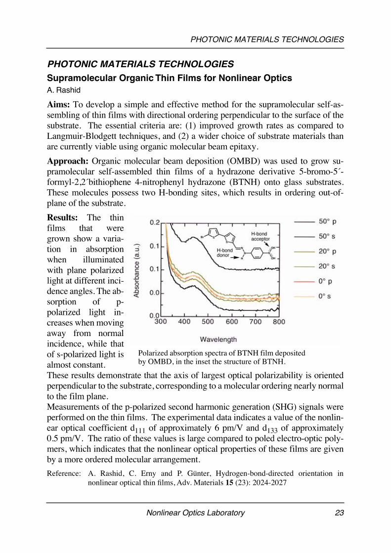
Results: The thinfilms that weregrown show a varia-tion in absorptionwhen illuminatedwith plane polarizedlight at different inci-dence angles. The ab-sorption of p-polarized light in-creases when movingaway from normalincidence, while thatof s-polarized light isalmost constant.These results demonstrate that the axis of largest optical polarizability is orientedperpendicular to the substrate, corresponding to a molecular ordering nearly normalto the film plane.Measurements of the p-polarized second harmonic generation (SHG) signals wereperformed on the thin films. The experimental data indicates a value of the nonlin-ear optical coefficient d111 of approximately 6 pm/V and d133 of approximately0.5 pm/V. The ratio of these values is large compared to poled electro-optic poly-mers, which indicates that the nonlinear optical properties of these films are givenby a more ordered molecular arrangement.
Reference: A. Rashid, C. Erny and P. Günter, Hydrogen-bond-directed orientation innonlinear optical thin films, Adv. Materials 15 (23): 2024-2027
Polarized absorption spectra of BTNH film depositedby OMBD, in the inset the structure of BTNH.
Nonlinear Optics Laboratory 23
PHOTONIC MATERIALS TECHNOLOGIES
Optical and Electrical Properties of Amorphous OrganicSemiconductors under Intense Electrical Excitation 3.2
P. Losio
Aims: To determine the basic physical parameters and arrangement for the realiza-tion of electrically pumped lasers based on organic semiconductors, by studyingtheir luminescence and optical absorption properties under intense electrical andoptical excitation.
Approach: We will investigate the absorption spectra, pholuminescence and elec-troluminescence spectra in organic semiconductors excited by short (100 ns) highvoltage (up to 1 kV) pulses and ultraviolet light to observe changes in the presenceof charges. All experiments will be conducted in our Ultra-High Vacuum (UHV)system and at low temperatures to avoid degradation of the samples and to maintainohmic injection at the contacts. A waveguide geometry will allow to increase theinteraction length between probing beam and injected charges.
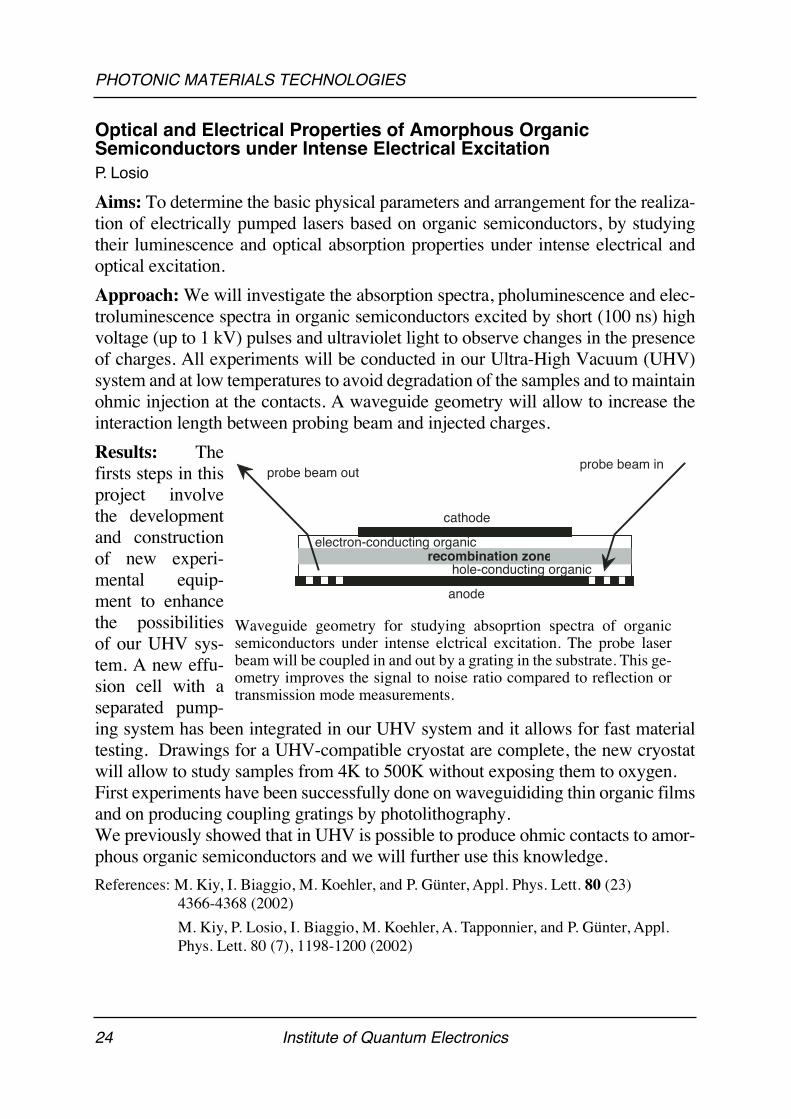
Results: Thefirsts steps in thisproject involvethe developmentand constructionof new experi-mental equip-ment to enhancethe possibilitiesof our UHV sys-tem. A new effu-sion cell with aseparated pump-ing system has been integrated in our UHV system and it allows for fast materialtesting. Drawings for a UHV-compatible cryostat are complete, the new cryostatwill allow to study samples from 4K to 500K without exposing them to oxygen. First experiments have been successfully done on waveguididing thin organic filmsand on producing coupling gratings by photolithography. We previously showed that in UHV is possible to produce ohmic contacts to amor-phous organic semiconductors and we will further use this knowledge.
References: M. Kiy, I. Biaggio, M. Koehler, and P. Günter, Appl. Phys. Lett. 80 (23) 4366-4368 (2002)
M. Kiy, P. Losio, I. Biaggio, M. Koehler, A. Tapponnier, and P. Günter, Appl. Phys. Lett. 80 (7), 1198-1200 (2002)
hole-conducting organic
electron-conducting organicrecombination zone
probe beam in
cathode
anode
probe beam out
Waveguide geometry for studying absoprtion spectra of organicsemiconductors under intense elctrical excitation. The probe laserbeam will be coupled in and out by a grating in the substrate. This ge-ometry improves the signal to noise ratio compared to reflection ortransmission mode measurements.
24 Institute of Quantum Electronics
PHOTONIC MATERIALS TECHNOLOGIES
Charge Injection and Transport in Amorphous Organic Semiconductors 3.3
A.Tapponnier
Aims: To improve the understanding of the in-trinsic charge transport properties in amorphousorganic semiconductors (small molecules) andof the charge-injection process at a clean metal-organic interface.
Approach: Organic field-effect transistor(FET) structures have been fabricated and char-acterized in ultrahigh vacuum (UHV). The ac-tive layer is formed by molecular beamdeposited organic molecules. Such devices al-low the study of relevant parameters such as thecharge carrier mobility, the level of doping andthe effect of impurity gases on those parame-ters.
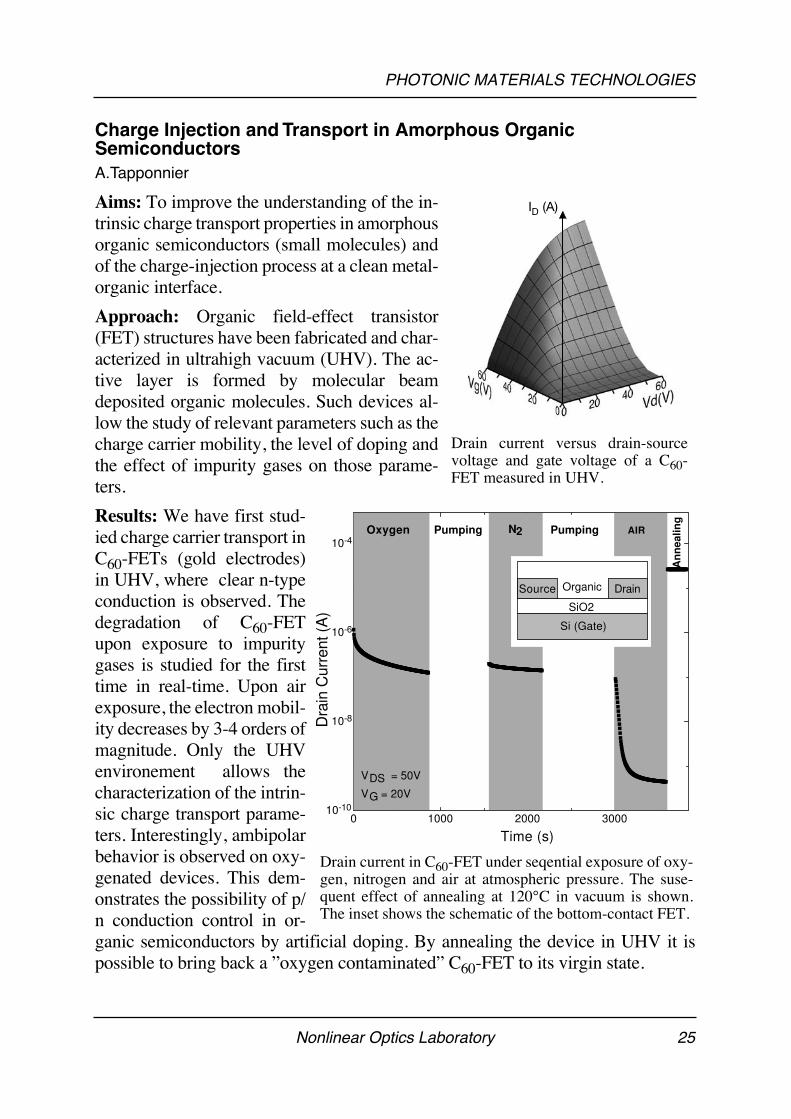
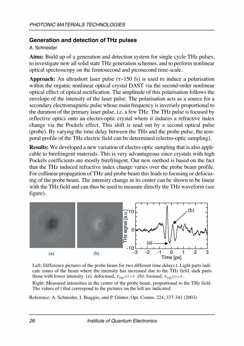
Results: We have first stud-ied charge carrier transport inC60-FETs (gold electrodes)in UHV, where clear n-typeconduction is observed. Thedegradation of C60-FETupon exposure to impuritygases is studied for the firsttime in real-time. Upon airexposure, the electron mobil-ity decreases by 3-4 orders ofmagnitude. Only the UHVenvironement allows thecharacterization of the intrin-sic charge transport parame-ters. Interestingly, ambipolarbehavior is observed on oxy-genated devices. This dem-onstrates the possibility of p/n conduction control in or-ganic semiconductors by artificial doping. By annealing the device in UHV it ispossible to bring back a ”oxygen contaminated” C60-FET to its virgin state.
Drain current versus drain-sourcevoltage and gate voltage of a C60-FET measured in UHV.
ID (A)
Time (s)
Dra
in C
urre
nt (
A)
0 1000 2000 300010-10
10-8
10-6
10-4
VG = 20V
VDS = 50V
An
nea
ling
Oxygen Pumping N2 AIRPumping
Si (Gate)
Source
SiO2
DrainOrganic
Drain current in C60-FET under seqential exposure of oxy-gen, nitrogen and air at atmospheric pressure. The suse-quent effect of annealing at 120°C in vacuum is shown.The inset shows the schematic of the bottom-contact FET.
Nonlinear Optics Laboratory 25
PHOTONIC MATERIALS TECHNOLOGIES
Generation and detection of THz pulses 3.4
A. Schneider
Aims: Build up of a generation and detection system for single cycle THz pulses,to investigate new all solid state THz generation schemes, and to perform nonlinearoptical spectroscopy on the femtosecond and picosecond time-scale.
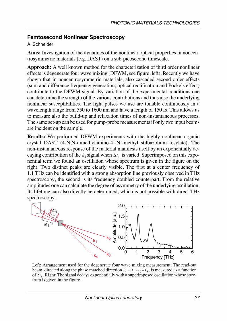
Approach: An ultrashort laser pulse (τ~150 fs) is used to induce a polarisationwithin the organic nonlinear optical crystal DAST via the second-order nonlinearoptical effect of optical rectification. The amplitude of this polarisation follows theenvelope of the intensity of the laser pulse. The polarisation acts as a source for asecondary electromagnetic pulse whose main frequency is inversely proportional tothe duration of the primary laser pulse, i.e. a few THz. The THz pulse is focused byreflective optics onto an electro-optic crystal where it induces a refractive indexchange via the Pockels effect. This shift is read out by a second optical pulse(probe). By varying the time delay between the THz and the probe pulse, the tem-poral profile of the THz electric field can be determined (electro-optic sampling).
Results: We developed a new variation of electro-optic sampling that is also appli-cable to birefringent materials. This is very advantageous since crystals with highPockels coefficients are mostly birefringent. Our new method is based on the factthat the THz induced refractive index change varies over the probe beam profile.For collinear propagation of THz and probe beam this leads to focusing or defocus-ing of the probe beam. The intensity change in its center can be shown to be linearwith the THz field and can thus be used to measure directly the THz waveform (seefigure).
Reference: A. Schneider, I. Biaggio, and P. Günter, Opt. Comm. 224, 337-341 (2003)
-3 -2 -1 0 1 2 3-10
0
10
Time [ps]
TH
z si
gnal
[a.u
.] (b)
(a)
Left: Difference pictures of the probe beam for two different time delays t. Light parts indi-cate zones of the beam where the intensity has increased due to the THz field, dark partsthose with lower intensity. (a): defocused, ;(b): focused, .
Right: Measured intensities in the center of the probe beam, proportional to the THz field.The values of t that correspond to the pictures on the left are indicated.
ETHz t( ) 0< ETHz t( ) 0>
(a) (b)
26 Institute of Quantum Electronics
PHOTONIC MATERIALS TECHNOLOGIES
Femtosecond Nonlinear Spectroscopy 3.5
A. Schneider
Aims: Investigation of the dynamics of the nonlinear optical properties in noncen-trosymmetric materials (e.g. DAST) on a sub-picosecond timescale.
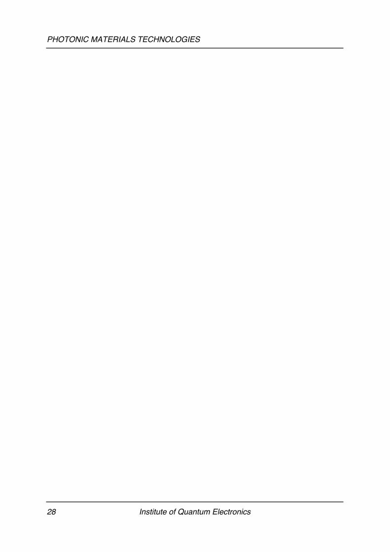
Approach: A well known method for the characterization of third order nonlineareffects is degenerate four wave mixing (DFWM, see figure, left). Recently we haveshown that in noncentrosymmetric materials, also cascaded second order effects(sum and difference frequency generation; optical rectification and Pockels effect)contribute to the DFWM signal. By variation of the experimental conditions onecan determine the strength of the various contributions and thus also the underlyingnonlinear susceptibilities. The light pulses we use are tunable continuously in awavelength range from 550 to 1600 nm and have a length of 150 fs. This allows usto measure also the build-up and relaxation times of non-instantaneous processes.The same set-up can be used for pump-probe measurements if only two input beamsare incident on the sample.
Results: We performed DFWM experiments with the highly nonlinear organiccrystal DAST (4-N,N-dimethylamino-4’-N’-methyl stilbazolium tosylate). Thenon-instantaneous response of the material manifests itself by an exponentially de-caying contribution of the signal when is varied. Superimposed on this expo-nential term we found an oscillation whose spectrum is given in the figure on theright. Two distinct peaks are clearly visible. The first at a center frequency of1.1 THz can be identified with a strong absorption line previously observed in THzspectroscopy, the second is its frequency doubled counterpart. From the relativeamplitudes one can calculate the degree of asymmetry of the underlying oscillation.Its lifetime can also directly be determined, which is not possible with direct THzspectroscopy.
k4 ∆t1
k1
k3
k2
k4
∆t1
∆t2
0 1 2 3 4 5 60.0
0.5
1.0
1.5
2.0
Frequency [THz]
Am
plitu
de [a
.u.]
Left: Arrangement used for the degenerate four wave mixing measurement. The read-outbeam, directed along the phase matched direction , is measured as a functionof . Right: The signal decays exponentially with a superimposed oscillation whose spec-trum is given in the figure.
k4 k1 k2– k3+=
∆t1
Nonlinear Optics Laboratory 27
PHOTONIC MATERIALS TECHNOLOGIES
28 Institute of Quantum Electronics
BLUE AND UV SOLID STATE LASERS
BLUE AND UV SOLID STATE LASERSFrequency Doubled Diode Pumped Solid-State Lasers 4.1
R. Cudney, F. Sulser, S. Barman and C. Medrano
Aims: We investigate optimized configurations of all solid state diode pumped fre-quency doubled lasers. The laser materials that were investigated are chromium-doped colquiriites: Cr:LiSAF, Cr:LiCAF and Cr:LiSGaF. Efficiency, stability andother physical parameters were investigated with respect to their suitability as laserhosts for optical frequency conversion based on KNbO3 crystals and KNbO3waveguides. Our approach is to diode-pump a solid-state laser that emits radiationat the adequate wavelength for frequency conversion. Among the laser materials wechose Cr:LiSAF, which can be pumped with 670-690 nm light, and has the stron-gest emission at 860 nm. Cheap and efficient laser diodes cover this region. For thedoubling we use KNbO3 crystals and waveguides.
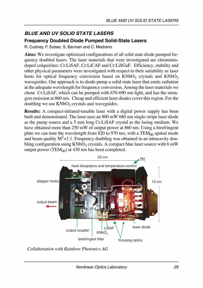
Results: A compact-infrared-tunable laser with a digital power supply has beenbuilt and demonstrated. The laser uses an 800 mW 680 nm single-stripe laser diodeas the pump source and a 5 mm long Cr:LiSAF crystal as the lasing medium. Wehave obtained more than 250 mW of output power at 860 nm. Using a birefringentplate we can tune the wavelength from 820 to 970 nm, with a TEM00 spatial modeand beam quality M2<1.1. Frequency doubling was obtained in an intracavity dou-bling configuration using KNbO3 crystals. A compact blue laser source with 6 mWoutput power (TEM00) at 430 nm has been completed.
Collaboration with Rainbow Photonics AG
birefringent filter
output coupler
focusing optics
laser diodeLiSAFKNbO3
23 cm
output beam
heat dissipators and temperature control
fan
stepper motor 13 cm
Nonlinear Optics Laboratory 29
BLUE AND UV SOLID STATE LASERS
Compact Blue Light Sources Using KNbO3 Waveguides 4.2
R. Degl’Innocenti and C. Medrano
Aims: Realisation of a compact blue laser source based on optical frequency con-version using waveguides in nonlinear optical crystals such as potassium niobate(KNbO3) with high efficient optical frequency doubling. Waveguides of typicallength of 1-2 cm can be combined with a diode and mounted together in a compactlaser device. Optimization of the arrangement for efficient compact blue source willbe investigated.
Approach: Refractive index changes, required for producing optical waveguides,are obtained via He+ or H+ single and multiple implantations. Ridge structures ofphotoresist are created on top of planar waveguides with standard photolithographyprocess and subsequently we proceed with a plasma etching process which finallyproduces the final structures in our material (for further details see reference) .Theefficiency of the optical frequency doubling depends also critically from the lossesof the waveguides and from geometrical factors as well: attenuation ≤ 3 dB/cm arerequired. Investigation of waveguide absorption, of the refractive index barrier pro-file induced by ion implantation and of the smoothness of the ridges are carried outin order to characterize and optimize the nonlinear process.
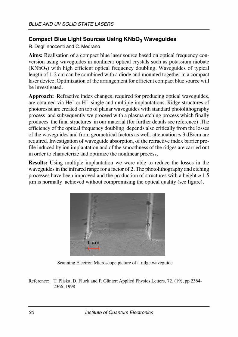
Results: Using multiple implantation we were able to reduce the losses in thewaveguides in the infrared range for a factor of 2. The photolithography and etchingprocesses have been improved and the production of structures with a height ≥ 1.5µm is normally achieved without compromising the optical quality (see figure).
Reference: T. Pliska, D. Fluck and P. Günter: Applied Physics Letters, 72, (19), pp 2364-2366, 1998
1 mm
Scanning Electron Microscope picture of a ridge waveguide
30 Institute of Quantum Electronics
BLUE AND UV SOLID STATE LASERS
Nonlinear Optics Laboratory 31
Compact Blue Light Sources Using KNbO3 and Cr:LiSAF Waveguides0.1
A.Majkic and C.Medrano
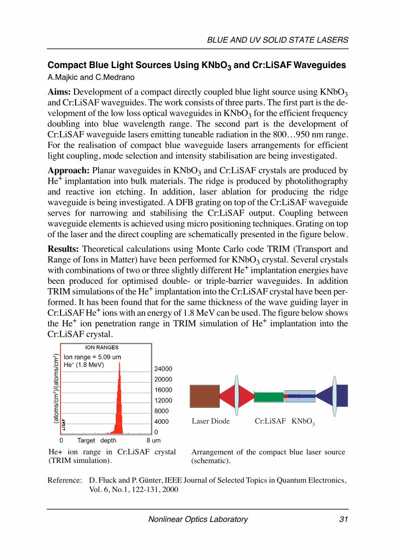
Aims: Development of a compact directly coupled blue light source using KNbO3and Cr:LiSAF waveguides. The work consists of three parts. The first part is the de-velopment of the low loss optical waveguides in KNbO3 for the efficient frequencydoubling into blue wavelength range. The second part is the development ofCr:LiSAF waveguide lasers emitting tuneable radiation in the 800…950 nm range.For the realisation of compact blue waveguide lasers arrangements for efficientlight coupling, mode selection and intensity stabilisation are being investigated.
Approach: Planar waveguides in KNbO3 and Cr:LiSAF crystals are produced byHe+ implantation into bulk materials. The ridge is produced by photolithographyand reactive ion etching. In addition, laser ablation for producing the ridgewaveguide is being investigated. A DFB grating on top of the Cr:LiSAF waveguideserves for narrowing and stabilising the Cr:LiSAF output. Coupling betweenwaveguide elements is achieved using micro positioning techniques. Grating on topof the laser and the direct coupling are schematically presented in the figure below.
Results: Theoretical calculations using Monte Carlo code TRIM (Transport andRange of Ions in Matter) have been performed for KNbO3 crystal. Several crystalswith combinations of two or three slightly different He+ implantation energies havebeen produced for optimised double- or triple-barrier waveguides. In additionTRIM simulations of the He+ implantation into the Cr:LiSAF crystal have been per-formed. It has been found that for the same thickness of the wave guiding layer inCr:LiSAF He+ ions with an energy of 1.8 MeV can be used. The figure below showsthe He+ ion penetration range in TRIM simulation of He+ implantation into theCr:LiSAF crystal.
Reference: D. Fluck and P. Günter, IEEE Journal of Selected Topics in Quantum Electronics, Vol. 6, No.1, 122-131, 2000
Laser Diode Cr:LiSAF KNbO3
Arrangement of the compact blue laser source(schematic).
He+ ion range in Cr:LiSAF crystal(TRIM simulation).
BLUE AND UV SOLID STATE LASERS
UV Solid State Waveguide Lasers 4.3
R. Degl’Innocenti and C. Medrano.
Aims: Production and investigation of a compact UV laser source by the optical fre-quency doubling of a green-emitting solid-state laser, using in a nonlinear crystalsuch as b-BaB2O4 or other borates.
Approach: Waveguides are produced via He+ implantation, which creates a de-creased refractive index barrier, and laser ablation. The borates are nonlinear opticalcrystals which exhibit a transparent frequency range down to 190 nm (BaB2O4) oreven lower therefore permitting optical frequency doubling in the UV: because theyare in general sensitive to moisture an approach different from photolithography isrequired. Femtosecond laser pulses could be used to structure ridges on top of thecrystals.
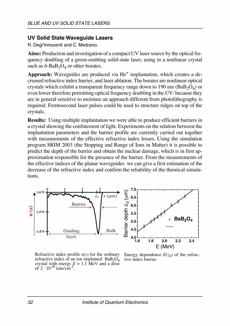
Results: Using multiple implantation we were able to produce efficient barriers ina crystal showing the confinement of light. Experiments on the relation between theimplantation parameters and the barrier profile are currently carried out togetherwith measurements of the effective refractive index losses. Using the simulationprogram SRIM 2003 (the Stopping and Range of Ions in Matter) it is possible topredict the depth of the barrier and obtain the nuclear damage, which is in first ap-proximation responsible for the presence of the barrier. From the measurements ofthe effective indices of the planar waveguides we can give a first estimation of thedecrease of the refractive index and confirm the reliability of the theorical simula-tions.
n (
z)
Guiding Bulk
Barrier
z (mm)1.675
1.475
1.575
z0
1 2 30
layer
Energy dependence E(z0) of the refrac-tive index barrier.
Refractive index profile n(z) for the ordinaryrefractive index of an ion implanted BaB2O4crystal with energy E = 1.1 MeV and a doseof 16 ions/cm 2.2 10⋅
32 Institute of Quantum Electronics
Publications 2003
PUBLICATIONS 2003Journal Publications
S. Concilio, I. Biaggio, P. Günter, S.P. Piotto, M.J. Edelmann, J.-M. Raimundo and F. Diederich“Third-order Nonlinear Optical Properties of In-backbone Substituted Oligo(triacetylene) Chromophores”J. Opt. Soc. Am. B 20 (8), 1656-1660 (2003)Ph. Dittrich, R. Bartlome, G. Montemezzani and P. Günter“Femtosecond Laser Ablation of DAST”Applied Surface Science 220, 88-95 (2003)D. Haertle, G. Caimi, A. Haldi, G. Montemezzani, P. Günter, A.A. Grabar, I.M. Stoika, Yu.M. Vysochanskii"Electro-optical Properties of Sn2P2S6"Optics Communications 215 (4-6), 333-343 (2003)B. Jagadish, M.D. Carducci, Ch. Bosshard, P. Günter, J.I. Margolis, L.J. Williams and E.A. Mash“Organic Crystal Engineering with Piperazine-2,5-diones. 4. Crystal Packing of Piperazinediones Derived from 2-Amino-7-cyano-4-methoxyindan-2-carboxylic Acid”Crystal Growth & Design 3 (5), 811-821 (2003)M. Jazbinsek, G. Montmezzani, P. Günter, A.A. Grabar, I.M. Stoika and Yu.M. Vysochanskii“Fast Near-infrared Self-pumped Phase Conjugation with Photorefractive Sn2P2S6”J. Opt. Soc. Am. B 20 (6), 1241-1246 (2003)M. Jazbinsek, M. Zgonik, M. Lee, S. Takekawa, K. Kitamura and H. Hatano“Optimization of Non-Volatile Two-Color Holographic Recording in Near-Stoichiometric LiNbO3”Ferroelectrics 296, 37-46 (2003)M. Koehler and I. Biaggio“Influence of Diffusion, Trapping, and State Filling on Charge Injection and Transport in Organic Insulators”Physical Review B 68, 075205-1-8 (2003)O-P. Kwon, S.-H. Lee, G. Montemezzani and P. Günter“Layer Structured Photoconducting Polymers: A New Class of Photorefractive Materials”Adv. Funct. Mater. 13 (6), 434-438 (2003)O-P. Kwon, S-H. Lee, G. Montemezzani and P. Günter“High Performance Photorefractive Materials Based on Layered Photoconductive Polymers”Polymeric Materials: Science & Engineering 88, 296-297 (2003)O-P. Kwon, S.-H. Lee, G. Montemezzani and P. Günter“Highly Efficient Photorefractive Composites Based on Layered Photoconductive Polymers”J. Opt. Soc. Am. B 20 (11), 2307-2312 (2003)
Nonlinear Optics Laboratory 33
Publications 2003
O-P. Kwon, G. Montemezzani, P. Günter and S.-H. Lee“High-gain Photorefractive Reflection Gratings in Layered Photoconductive Polymers”Appl. Phys. Lett. 84 (1), 43-45 (2004)P. Lavéant, C. Medrano, B. Ruiz and P. Günter“Growth of Nonlinear Optical DAST Crystals”Chimia 57 (6), 349-351 (2003)L. Mutter, M. Jazbinsek, M. Zgonik, U. Meier, Ch. Bosshard and P. Günter“Photobleaching and Optical Properties of Organic Crystal 4-N, N-Dimethylamino-4’-N’-Methyl Stilbazolium Tosylate”J. Appl. Phys. 94 (3), 1356-1361 (2003)M. Raimundo, S. Lecomte, M.J. Edelmann, S. Concilio, I. Biaggio, Ch. Bosshard, P. Günter and F. Diederich“Synthesis and Properties of a ROMP Backbone Polymer with Efficient, Laterally Appended Nonlinear Optical Chromophores”J. Mater. Chem. 14, 292-295 (2004)A. Rashid, Ch. Erny and P. Günter“Hydrogen-Bond-Directed Orientation in Nonlinear Optical Thin Films”Advanced Materials 15 (23), 2024-2027 (2003)J. Santos, E.A. Mintz, O. Zehnder, Ch. Bosshard, X.R. Bu and P. Günter“New Class of Imidazoles Incorporated with Thiophenevinyl Conjugation Pathway for Robust Nonlinear Optical Chromophores”Tetrahedron Letters 42, 805-808 (2001)A. Schneider, I. Biaggio and P. Günter“Optimized Generation of THz Pulses via Optical Rectification in the Organic Salt DAST”Optics Communications 224, 337-341 (2003)A. Tapponnier, I. Biaggio, M. Koehler and P. Günter“Integrated Pulsed Photoconductivity of Organic Light Emitting Diodes”Appl. Phys. Lett. 83 (26), 5473-5475 (2003)M. Wintermantel and I. Biaggio“Temperature-dependent Electron Mobility and Large Polaron Interpretation in Bi12SiO20”Phys. Rev. B 67, 165108-1 - 165108-6 (2003)
Conference PublicationsPh. Dittrich, G. Montemezzani and P. Günter“Interband Photorefraction for Tunable Optical Filters at Telecom Wavelength”OSA Trends in Optics and Photonics, Vol. 87“Photorefractive Effects, Materials, and Devices” Ph. Delaye, C. Denz, L. Mager and G. Montemezzani, eds. (Optical Society of America, Washington D.C.), 620-624 (2003)
34 Institute of Quantum Electronics
Publications 2003
A.A. Grabar, I.V. Kedyk, I.M. Stoika, Yu.M. Vysochanskii, M. Jazbinsek, G. Montemezzani and P. Günter"Enhanced photorefractive Properties of Te-Doped Sn2P2S6"OSA Trends in Optics and Photonics, Vol. 87“Photorefractive Effects, Materials, and Devices” Ph. Delaye, C. Denz, L. Mager and G. Montemezzani, eds. (Optical Society of America, Washington D.C.), 10-14 (2003)D. Haertle, G. Caimi, A. Haldi, G. Montemezzani, P. Günter, A.A. Grabar, I.M. Stoika, Yu.M. Vysochanskii"Electro-optical Properties of Photorefractive Sn2P2S6"OSA Trends in Optics and Photonics, Vol. 87“Photorefractive Effects, Materials, and Devices” Ph. Delaye, C. Denz, L. Mager and G. Montemezzani, eds. (Optical Society of America, Washington D.C.), 73-78 (2003)M. Jazbinsek, D. Haertle, G. Montemezzani, P. Günter, A.A. Grabar, I.M. Stoika and Yu. M. Vysochanskii“Sn2P2S6 Crystals for Fast Near Infrared Photorefraction and Phase Conjugation”OSA Trends in Optics and Photonics, Vol. 87“Photorefractive Effects, Materials, and Devices” Ph. Delaye, C. Denz, L. Mager and G. Montemezzani, eds. (Optical Society of America, Washington D.C.), 190-194 (2003)O-P. Kwon, G. Montemezzani, P. Günter and S.-H. Lee“High Performance Layered Photorefractive Polymers in Reflection Grating Geometry”OSA Trends in Optics and Photonics, Vol. 87“Photorefractive Effects, Materials, and Devices”Ph. Delaye, C. Denz, L. Mager and G. Montemezzani, eds. (Optical Society of America, Washington D.C.), 262-266 (2003)
Nonlinear Optics Laboratory 35
Presentations 2003
PRESENTATIONS 2003* = invited talk
Ph. Dittrich“Tunable Optical Filters at Telecom Wavelengths by Interband Photorefractive Gratings”CLEO USA, Baltimore, USA1.-6.6.03Ph. Dittrich“Interband Photorefraction for Tunable Optical Filters”Topical Meeting on Photorefractive Effects, Materials, and Devices (PR’03), La Colle sur Loup, F17.-21.6.03Ph. Dittrich“Femtosecond Laser Ablation of the Nonlinear Optical Organic Crystal DAST”CLEO Europe 2003, Munich, D23.-27.6.03A. Grabar, I Kedyk, I. Stoika, Yu.M. Vysochanskii, M. Jazbinsek, G. Montemezzani, P. Günter“Enhanced Photorefractive Properties of Te-doped Sn2P2S6”Topical Meeting on Photorefractive Effects, Materials, and Devices (PR’03), La Colle sur Loup, F17.-21.6.03
* P. Günter“Organic Crystals, Electro-optics and the Generation of THz Waves”Frühjahrstagung des Arbeitskreises Festkörperphysik der Deutschen Physikalischen Gesellschaft, Dresden, D24.-28.3.03
* P. Günter“Organic Crystals, Electro-optics and the Generation of THz Waves”“Banfi Memorial Workshop on Nonlinear Optics and Lasers, Pavia, I16.6.03
* P. Günter“Polar Organic Nonlinear Optical Crystals for Electro-optics”Romanian Conference on Advanced Materials – ROCAM 2003, Constanta, Romania15.-18.9.03
* P. Günter“Nonlinear Optics with Organic Materials”39th Course of the International School of Quantum Electronics, Erice, I18.-25.10.03
* P. Günter“Organic Materials in Electro-optical Devices”39th Course of the International School of Quantum Electronics, Erice, I18.-25.10.03
36 Institute of Quantum Electronics
Presentations 2003
* P. Günter“Electro-optics in VLSI Photonics Using DAST Crystals”7th International Conference on Organic Nonlinear Optics and Organic Electronics (ICONO’7), Sorak, Korea4.-8.11.03
* P. Günter“Nonlinera Optical Effects and Applications”Seminar Ajou University, Suwon, Korea10.11.03
* P. Günter“Progress in Organic Materials for Microresonators”EU Progress Meeting (NAIS, IST), Brussels, B25.12-03D. Haertle“Electro-optical Properties of Photorefractive Sn2P2S6”Topical Meeting on Photorefractive Effects, Materials, and Devices (PR’03), La Colle sur Loup, F17.-21.6.03M. Jazbinsek“Sn2P2S6 Crystals for Fast Infrared Photorefraction and Phase Conjugation”Topical Meeting on Photorefractive Effects, Materials, and Devices (PR’03), La Colle sur Loup, F17.-21.6.03O-P. Kwon, S.H. Lee, G. Montemezzani, P. Günter“High Performance Photorefractive Materials Based on Layered Photoconductive Polymers”American Chemical Society National Meeting, New Orleans, USA23.-27.3.03O-P. Kwon, S.H. Lee, G. Montemezzani, P. Günter“Photorefractive Properties of Layer Structured Polymer Composites”Korean Polymer Society Meeting, Seoul, Korea11.-12.4.03O-P. Kwon, G. Montemezzani, P. Günter, S.H. Lee“Highly Efficient Photorefractive Materials Based on Layer Structured Polymers”7th International Conference on Organic Nonlinear Optics (ICONO-7), Sorak, Korea4.-8.11.03P. Lavéant“Growth of High Quality Crystals for Nonlinear Optics”E-MRS 2003, Strasbourg, F10.-13.6.03
* G. Montemezzani"Low Intensity Photorefractive Nonlinear Optics for Dynamic Holography and Applications"Mid Sweden University, Sundsvall, S28.1.03
Nonlinear Optics Laboratory 37
Presentations 2003
* G. Montemezzani“Photorefractive Effects and Light Diffractor in Strongly Anisotropic Materials”6th Mediterranean Workshop and Topical Meeting “Novel Optical Materials and Applications (NOMA’03), Cetraro, I8.-13.6.03G. Montemezzani“High Performance Layered Photorefractive Polymers in Reflection Grating Geometry”Topical Meeting on Photorefractive Effects, Materials and Devices (PR’03), La Colle sur Loup, F17.-21.6.03
* G. Montemezzani“Fast Near Infrared Photorefraction and Phase Conjugation in Sn2P2S6”CLEO Europe 2003, Munich, D23.-27.6.03G. Montemezzani“Layered Structure Photoconductive Polymers: A new Class of Photorefractive Composites”CLEO Europe 2003, Munich, D23.-27.6.03
* G. Montemezzani“Conventional and Interband Photorefraction in Inorganic Crystals”Ajou University, Suwon, South-Korea4.7.03G. Montemezzani“Sn2P2S6 Crystals for Near Infrared Processing and Wave Manipulation”COST P8 Working Group Meeting, Angers, F4.-5.9.03
* G. Montemezzani“Effets Photoréfractifs dans Matériaux Inorganiques et Organiques”MOPS, Université de Metz et Supélec, Metz, F23.9.03
* A. Rashid“Origin and Supramolecular Ordering in Nonlinear Optical Thin Films”E-MRS 2003, Strasbourg, F10.-13.6.03B. Ruiz“Growth of DAST Thin Films Crystals”E-MRS 2003, Strasbourg, F10.-13.6.03A. Schneider“Velocity-matched Generation of Terahertz Pulses in the Organic Crystal DAST”CLEO Europe2003, Munich, D23.-27.6.03
38 Institute of Quantum Electronics
PHD THESES IN PHYSICS 2003
PHD THESES IN PHYSICS 2003
PHD Thesis
Dittrich, Philipp“Ultraviolet Interband Photorefraction for Dynamic Waveguides and Filters, and Femtosecond Photo-structuring”ETH Nr. 15414 (Prof. Dr. P. Günter, Prof. Dr. T. Esslinger & PD Dr. G. Montemezzani)
Korreferate
Fischer, Cornelia"Trace-Gas Sensing with a Pulsed Difference Frequency Laser Spectrometer and Three Different Detection Schemes"ETH Nr. 15350 (Prof.Dr. M. Sigrist & Prof. Dr. P. Günter)
Guerrero, Gilles"Active Photonic Crystals Implemented with Phase-Locked Arrays of VCSELs"EPFL (Prof. Dr. E. Kapon, Prof. Dr. R. Dändliker, Prof. Dr. A. Forchel, Prof. Dr. P. Günter)
Nonlinear Optics Laboratory 39
DIPLOMA THESES IN PHYSICS 2003
DIPLOMA THESES IN PHYSICS 2003Bartlome, Richard"Harmonic Emission from the Rear Side of Overdense Thin Foils Irradiated at Near Relativistic Intensities"ETH Zürich & Max-Planck Institut, Garching, June 2003(Prof. Dr. P. Günter & Prof. Dr. K. Witte)
Clausen, Pascal"Quantum Wire Light Emitting Diode"ETH Zürich & EPFL Lausanne, March 2003(Prof. Dr. P. Günter & Prof. Dr. E. Kapon)
Haldi, Andreas"Hole Mobility of 2.7-Bis(diarylamino)-9.9-Dimethylfluorenes (TPF) Doped into Poly(styrene)"ETH Zürich & University of Arizona, Tucson, March 2003(Prof. Dr. P. Günter & Prof. Dr. B. Kippelen)
Walser, Andreas"Grating Stabilized Blue Solid State Laser"ETH Zürich, March 2003(Prof. Dr. P. Günter)
40 Institute of Quantum Electronics