Embed Size (px)
Citation preview

®
5220ATransconductance Amplifier
Instruction Manual
PN 491936June 1979 Rev. 3, 6/97© 1997 Fluke Corporation. All rights reserved. Printed in USAAll product names are trademarks of their respective companies.

LIMITED WARRANTY AND LIMITATION OF LIABILITY
Each Fluke product is warranted to be free from defects in material and workmanship undernormal use and service. The warranty period is one year and begins on the date of shipment.Parts, product repairs, and services are warranted for 90 days. This warranty extends only to theoriginal buyer or end-user customer of a Fluke authorized reseller, and does not apply to fuses,disposable batteries, or to any product which, in Fluke’s opinion, has been misused, altered,neglected, contaminated, or damaged by accident or abnormal conditions of operation orhandling. Fluke warrants that software will operate substantially in accordance with its functionalspecifications for 90 days and that it has been properly recorded on non-defective media. Flukedoes not warrant that software will be error free or operate without interruption.
Fluke authorized resellers shall extend this warranty on new and unused products to end-usercustomers only but have no authority to extend a greater or different warranty on behalf of Fluke.Warranty support is available only if product is purchased through a Fluke authorized sales outletor Buyer has paid the applicable international price. Fluke reserves the right to invoice Buyer forimportation costs of repair/replacement parts when product purchased in one country is submittedfor repair in another country.
Fluke’s warranty obligation is limited, at Fluke’s option, to refund of the purchase price, free ofcharge repair, or replacement of a defective product which is returned to a Fluke authorizedservice center within the warranty period.
To obtain warranty service, contact your nearest Fluke authorized service center to obtain returnauthorization information, then send the product to that service center, with a description of thedifficulty, postage and insurance prepaid (FOB Destination). Fluke assumes no risk for damage intransit. Following warranty repair, the product will be returned to Buyer, transportation prepaid(FOB Destination). If Fluke determines that failure was caused by neglect, misuse, contamination,alteration, accident, or abnormal condition of operation or handling, including overvoltage failurescaused by use outside the product’s specified rating, or normal wear and tear of mechanicalcomponents, Fluke will provide an estimate of repair costs and obtain authorization beforecommencing the work. Following repair, the product will be returned to the Buyer transportationprepaid and the Buyer will be billed for the repair and return transportation charges (FOBShipping Point).
THIS WARRANTY IS BUYER'S SOLE AND EXCLUSIVE REMEDY AND IS IN LIEU OF ALLOTHER WARRANTIES, EXPRESS OR IMPLIED, INCLUDING BUT NOT LIMITED TO ANYIMPLIED WARRANTY OF MERCHANTABILITY OR FITNESS FOR A PARTICULAR PURPOSE.FLUKE SHALL NOT BE LIABLE FOR ANY SPECIAL, INDIRECT, INCIDENTAL, ORCONSEQUENTIAL DAMAGES OR LOSSES, INCLUDING LOSS OF DATA, ARISING FROMANY CAUSE OR THEORY.
Since some countries or states do not allow limitation of the term of an implied warranty, orexclusion or limitation of incidental or consequential damages, the limitations and exclusions ofthis warranty may not apply to every buyer. If any provision of this Warranty is held invalid orunenforceable by a court or other decision-maker of competent jurisdiction, such holding will notaffect the validity or enforceability of any other provision.
Fluke CorporationP.O. Box 9090Everett, WA 98206-9090U.S.A.
Fluke Europe B.V.P.O. Box 11865602 BD EindhovenThe Netherlands
11/99
i
Table of Contents
Section Title Page
1 Introduction and Specifications........................................................ 1-1
1-1. Introduction .......................................................................................... 1-11-2. Specifications ....................................................................................... 1-2
2 Operating Instructions....................................................................... 2-1
2-1. Introduction .......................................................................................... 2-12-2. Shipping Information............................................................................ 2-12-3. Input Power .......................................................................................... 2-12-4. Fuse Replacement................................................................................. 2-22-5. AC Line Fuse ................................................................................... 2-22-6. Power Supply Fuses ......................................................................... 2-22-7. Rack Installation................................................................................... 2-22-8. Operating Features................................................................................ 2-22-9. Operating Notes.................................................................................... 2-52-10. AC Line Connection ........................................................................ 2-52-11. Transconductance Amplifier ............................................................ 2-52-12. Input Voltage Requirements ............................................................ 2-52-13. Input Voltage Selection, Front/Rear ................................................ 2-62-14. Current Output, Front/Rear .............................................................. 2-62-15. Standby/Operate............................................................................... 2-62-16. Local/Remote ................................................................................... 2-62-17. Status Indicators ............................................................................... 2-62-18. Audible Output................................................................................. 2-72-19. Inductive Loads................................................................................ 2-72-20. Operation .............................................................................................. 2-9
3 Theory of Operation........................................................................... 3-1
3-1. Introduction .......................................................................................... 3-13-2. Overall Functional Description ............................................................ 3-13-3. General ............................................................................................. 3-13-4. Analog Section................................................................................. 3-13-5. Digital Section.................................................................................. 3-43-6. Circuit Analysis .................................................................................... 3-43-7. Power Supply ................................................................................... 3-4

5220AInstruction Manual
ii
3-8. Preamplifier...................................................................................... 3-63-9. A6 Driver ......................................................................................... 3-73-10. A7 Output......................................................................................... 3-93-11. A8 Analog Control........................................................................... 3-103-12. A9 Front Panel ................................................................................. 3-113-13. A10 Logic ........................................................................................ 3-113-14. Reset Logic .................................................................................. 3-113-15. Timing Logic ............................................................................... 3-133-16. Standby/Operate Logic ................................................................ 3-143-17. Local/Remote Logic .................................................................... 3-153-18. Front/Rear Input Logic ................................................................ 3-153-19. Failure Status Logic ..................................................................... 3-163-20. A11 MIS Bus Interface .................................................................... 3-16
4 Maintenance ....................................................................................... 4-1
4-1. Introduction .......................................................................................... 4-14-2. Service Information .............................................................................. 4-24-3. General Maintenance............................................................................ 4-24-4. Cleaning ........................................................................................... 4-24-5. Air Filter Maintenance ..................................................................... 4-24-6. Access Information .......................................................................... 4-24-7. Internal Components/Assemblies ................................................ 4-44-8. Front Panel Removal ................................................................... 4-44-9. A9 Front Panel PCB Removal ..................................................... 4-44-10. A2 Transformer Assembly Removal ........................................... 4-44-11. A6 Driver and A7 Output Assembly Removal ............................ 4-54-12. A3 Cap Bus Removal .................................................................. 4-54-13. A12 Shunt Assembly Removal.................................................... 4-54-14. Fuse Replacement ............................................................................ 4-64-15. Ac Line Fuse................................................................................ 4-64-16. Power Supply Fuses..................................................................... 4-64-17. Line Voltage Selection..................................................................... 4-64-18. Output Terminal Selection, Front/Rear............................................ 4-74-19. Service Tools.................................................................................... 4-84-20. Performance Test.................................................................................. 4-84-21. Initial Conditions.............................................................................. 4-84-22. Front Panel Tests.............................................................................. 4-94-23. Zero Output ...................................................................................... 4-94-24. DC Accuracy and Line Regulation .................................................. 4-104-25. Harmonic Distortion......................................................................... 4-104-26. Frequency Response......................................................................... 4-114-27. Overcurrent Trip Test....................................................................... 4-114-28. Overvoltage Trip Test ...................................................................... 4-124-29. Calibration Adjustments....................................................................... 4-124-30. Initial Conditions.............................................................................. 4-134-31. Input Offset Adjustment................................................................... 4-134-32. Driver Offset Adjustment................................................................. 4-134-33. Output Bias Adjustment................................................................... 4-144-34. DC Accuracy Adjustment ................................................................ 4-144-35. Frequency Response......................................................................... 4-144-36. Overcurrent Adjustment................................................................... 4-154-37. Overvoltage Adjustment .................................................................. 4-154-38. Replacement of Selected Components ................................................. 4-154-39. Resistors R11 and R12..................................................................... 4-16

Contents (continued)
iii
4-40. Resistor R13..................................................................................... 4-174-41. Troubleshooting.................................................................................... 4-18
5 List of Replaceable Parts................................................................... 5-1
5-1. Introduction .......................................................................................... 5-15-2. How to Obtain Parts ............................................................................. 5-15-3. Manual Status Information ................................................................... 5-25-4. Newer Instruments................................................................................ 5-25-5. Service Centers..................................................................................... 5-2
6 Option and Accessory Information................................................... 6-1
6-1. Introduction .......................................................................................... 6-16-2. Accessories ........................................................................................... 6-16-3. Rack Mounting Kit (M08-205-600)................................................. 6-16-4. Rack Slide Kit (M00-280-610) ........................................................ 6-36-5. Precision Y5020A Current Shunt..................................................... 6-3
7 Schematic Diagrams.......................................................................... 7-1

5220AInstruction Manual
iv

v
List of Tables
Table Title Page
1-1. Accessories ............................................................................................................ 1-21-2. Specifications......................................................................................................... 1-22-1. Controls, Indicators, and Connectors..................................................................... 2-43-1. Effect of Reset Command on A10 Logic and A9 Front Panel............................... 3-134-1. Required Test Equipment ...................................................................................... 4-14-2. DC Accuracy Test.................................................................................................. 4-104-3. Frequency Response Test ...................................................................................... 4-114-4. Replacement Resistors for R11 and R12 ............................................................... 4-174-5. Replacement Resistors for R13.............................................................................. 4-184-6. Mainframe and Digital Section Troubleshooting Guide........................................ 4-214-7. Analog Section Troubleshooting Guide................................................................. 4-255-1. 5220A Final Assembly .......................................................................................... 5-45-2. A1 Motherboard PCB Assembly ........................................................................... 5-175-3. A2 Power Transformer Assembly ......................................................................... 5-185-4. A3 Capacitor Bus PCB Assembly ......................................................................... 5-195-5. A4 Regulator PCB Assembly ................................................................................ 5-215-6. A5 Preamplifier PCB Assembly ............................................................................ 5-235-7. A6 Driver PCB Assembly...................................................................................... 5-265-8. A7 Output PCB Assembly ..................................................................................... 5-285-9. A8 Analog Control PCB Assembly ....................................................................... 5-315-10. A9 Front Panel PCB Assembly.............................................................................. 5-335-11. A10 Logic PCB Assembly..................................................................................... 5-345-12. A11 MIS Bus Interface PCB Assembly................................................................. 5-365-13. A12 Shunt Assembly ............................................................................................. 5-385-14. A13 Output Termination PCB Assembly .............................................................. 5-405-15. A14 Extender PCB Assembly................................................................................ 5-41

5220AInstruction Manual
vi
vii
List of Figures
Figure Title Page
5220A Transconductance Amplifier...................................................................... x1-1. Outline Drawings................................................................................................... 1-52-1. Controls, Indicators, and Connectors..................................................................... 2-32-2. Maximum Load Inductance vs Frequency............................................................. 2-82-3. Typical Transconductance Error for Inductive Loads ........................................... 2-93-1. 5220A Functional Block Diagram......................................................................... 3-23-2. Transconductance Amplifier Simplified Circuit Diagram..................................... 3-33-3. Power Supply Functional Block Diagram ............................................................. 3-53-4. A5 Preamplifier Functional Block Diagram .......................................................... 3-63-5. A6 Driver Functional Block Diagram.................................................................... 3-83-6. A7 Output Functional Block Diagram................................................................... 3-93-7. A8 Analog Control Simplified Block Diagram ..................................................... 3-103-8. A10 Logic Simplified Block Diagram................................................................... 3-123-9. Timing Sequence ................................................................................................... 3-143-10. A11 MIS Bus Interface .......................................................................................... 3-184-1. Internal Component/Assembly Locations.............................................................. 4-34-2. Line Voltage Selection........................................................................................... 4-74-3. Test Point Location/Identification ......................................................................... 4-194-4. Flowchart Summary of Mainframe and Digital Section Troubleshooting Guide.. 4-204-5. Flowchart Summary of Analog Section Troubleshooting Guide........................... 4-245-1. 5220A Final Assembly .......................................................................................... 5-85-2. A1 Motherboard PCB Assembly ........................................................................... 5-175-3. A2 Power Transformer Assembly ......................................................................... 5-185-4. A3 Capacitor Bus PCB Assembly ......................................................................... 5-205-5. A4 Regulator PCB Assembly ................................................................................ 5-225-6. A5 Preamplifier PCB Assembly ............................................................................ 5-255-7. A6 Driver PCB Assembly...................................................................................... 5-275-8. A7 Output PCB Assembly ..................................................................................... 5-295-9. A8 Analog Control PCB Assembly ....................................................................... 5-325-10. A9 Front Panel PCB Assembly.............................................................................. 5-335-11. A10 Logic PCB Assembly..................................................................................... 5-355-12. A11 MIS Bus PCB Assembly................................................................................ 5-375-13. A12 Shunt Assembly ............................................................................................. 5-395-14. A13 Output Termination PCB ............................................................................... 5-405-15. A14 Extender PCB Assembly................................................................................ 5-41

5220AInstruction Manual
viii
6-1. Rack Mounting Kit ................................................................................................ 6-26-2. Rack Slide Kit ........................................................................................................ 6-47-1. Interconnect Diagram............................................................................................. 7-27-2. Chassis Wiring....................................................................................................... 7-47-3. Power Supply......................................................................................................... 7-67-4. A5 Preamplifier PCB Assembly ............................................................................ 7-87-5. A6 Driver and A7 Output PCB Assemblies .......................................................... 7-107-6. A8 Analog Control PCB Assembly ....................................................................... 7-127-7. A9 Front Panel PCB Assembly.............................................................................. 7-147-8. A10 Logic PCB Assembly..................................................................................... 7-167-9. A11 MIS Bus Interface PCB Assembly................................................................. 7-18

Contents (continued)
ix
5220AInstruction Manual
x
ajs36f.eps
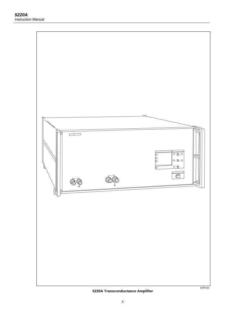
5220A Transconductance Amplifier

1-1
Section 1Introduction and Specifications
1-1. IntroductionThe Model 5220A is a transconductance amplifier designed to operate as either a standalone unit or an extension of the Fluke Model 5100 Series Calibrator. Functionally, theinstrument operates as a precision ac/dc current source for calibrating current shuntsand/or current meters. As the name (transconductance amplifier) implies, the outputcurrent level is a function of an input control voltage. The input/output ratio is establishedat 1:1 so that a voltage input in the range of -20 to +20 volts will produce a proportionalcurrent output of -20 to +20 amperes. Input voltages may be either dc or ac levels,depending on the output requirements. Bandwidth for ac operation is dc to 5 kHz.
Control of the 5220A can be handled locally using front panel controls or remotely byway of the 5100 Series Calibrator. (The 5100 must be equipped with a Model Y5000Interface.) Control mode selection is accomplished using two front-panel push buttonswitches, INPUT and LOCAL. The INPUT switch allows selection of either front or rearcontrol-voltage input connections. The LOCAL switch is used to recall the 5220A fromremote to local operation.
A series of front panel indicators are used to visually display both the control andoperating status of the 5220A. Control indicators include OPER (operate), STDBY(standby), FRONT input, REAR input, REMOTE, and LOCAL LOCKOUT. Thecombination of lit LEDs indicates the present status of the control mode. Status indicatorsinclude THERMAL CUT-OFF, OVER COMPLIANCE, and OVER CURRENT. Whenany one of these indicators is lit, an overload condition has been detected causing the5220A to switch to standby operation. All indicators are active regardless of the selectedcontrol mode, local or remote.
Current output connections are provided on both the front and rear panels. However, onlyone set of terminals is active. Selection of the desired set is accomplished internally andis, therefore, not considered an operator function. Neither local nor remote operation isaffected by the selection of front or rear output.
Forced-air circulation is incorporated in the 5220A to ensure adequate cooling of thecurrent output stage. Air is pulled in through a rear-panel filter, passed over the outputstage heat sink, and exhausted through the unit’s side panels.
The 5220A is designed to operate from ac line voltages within the range of 90 V ac to264 V ac, 50 to 60 Hz. One-of-eight specific voltages (100, 110, 115, 120, 200, 220, 230,240 V ac +10 %) can be selected to ensure compatibility with the local line voltage. The

5 220AInstruction Manual
1-2
selection switches are inside the 5220A. Refer to Section 4 of this manual for informationon how to properly set the line power switches.
Accessories available for use with the 5220A are listed and described in Table 1-1. Therack mounting kits are designed for use with a standard 19-inch equipment rack. TheModel Y5020A is a precision current shunt recommended for use in calibrating the5220A. Specify both model number and description when ordering accessories.
Table 1-1. Accessories
Model No. Description
M07-205-600 Rack Mounting Kit
M00-260-610 Rack Slide Kit, 18 in
M00-280-610 Rack Slide Kit, 24 in
Y5020 Precision Shunt
1-2. SpecificationsSpecifications for the Model 5220A are given in Table 1-2.
Table. 1-2. Specifications
Calibration Cycle All specifications are valid for a 180-day period at an operatingtemperature of 20 °C to 30 °C and a relative humidity of 70 % orless.
Basic
Transconductance 1 Siemen (1 ampere per volt)
Output Range 0 A to 20 A dc or rms ac (28.3 A peak)
Compliance Voltage ≥±4 V dc or 3 V rms ac (4.25 V peak)
DC Accuracy ±(0.025 % of output +1 mA)
AC Accuracy ±(0.05 % of output + 1 mA) from 30 Hz to 1 kHz, and ±(0.05 % ofoutput + 1 mA) x f from 1 kHz to 5 kHz, where f = frequency in kHz.
Short Term DC Stability Output changes less than ±(0.005 % + 200 µA) in 10 minutes, withconstant line, load, and temperature.
Short Term AC Stability Output changes less than ±(0.01 % + 500 µA) in 10 minutes, withconstant line, load, and temperature.
Harmonic Distortion and Noise ±(0.05 % of output ±1 mA rms) over frequency range of 30 Hz to 1kHz and measured with a noise bandwidth of 300 kHz, ±(0.05 % ofoutput + 1 mA) x f from 1 kHz to 5 kHz, where f = frequency in kHz.
Temperature Coefficient ±(0.0025 % of output + 100 µA) per degree C above 30 °C orbelow 20 °C.
Transient Recovery Output will settle to within 0.01 % of final value within 2 secondsfollowing a programmed change in output current or frequency(10 ms for 5220A alone).

Introduction and SpecificationsSpecifications 1
1-3
Table 1-2. Specifications (cont.)
Electromagnetic Compatibility This instrument is designed to operate in Standard Laboratoryenvironments where in electromagnetic environment is highlycontrolled. If used in areas with RF fields >0.4 V/m there could beerrors in measurement.
DC Mode (including 5100 Series B)
Output Range ±1 to ±19.9999 A
Accuracy of Output ±(0.025 % of selected output + 1 mA)
Resolution ±0.1 mA
Temperature Coefficient ±(0.003 % of selected output + 100 µA) / °C, above 30 °C andbelow 20 °C
Line Regulation Output changes less than 0.001 % for a ±10 % change in linevoltage.
Load Regulation Output changes less than ±(0.005 % + 0.3 mA) for a full loadchanges of 4 V of compliance.
AC Mode (including 5100 Series B)
Output Range 1 A rms to 19.9999 A rms
Accuracy of Output ±(0.07 % of selected output + 1 mA rms) from 50 Hz to 1 kHz,and ±(0.07 % of selected output + 1 mA rms) x f from 1 kHz to 5kHz, where f = frequency in kHz.
Resolution ±0.1 mA rms
Temperature Coefficient ±(0.003 % of selected output + 100 µA rms) per °C, above 30 °Cand below 20 °C.
Short Term Stability Output changes less than ±(0.02 % + 500 µA rms) in 10 minutes,with constant line, load, and temperature.
Harmonic Distortion and Noise ±(0.07 % of output + 1 mA rms) over frequency range of 30 Hz to1 kHz a noise bandwidth of 300 kHz, ±(0.07 % of output + 1 mA)x f from 1 kHz to 5 kHz, where f = frequency in Hz.
Line Regulation Output changes less than 0.005 % for ±10 % changes in linevoltage.
Load Regulation For frequencies less than 1 kHz:
±(0.005 % lout + 150 µA) per volt of output compliance voltage.
For frequencies greater than 1 kHz:
±(0.005 % lout + 150 µA) x f per volt of output compliancevoltage, where f = frequency in kHz.

5 220AInstruction Manual
1-4
Table 1-2. Specifications (cont.)
General
Load Capability Drives all resistive and capacitive loads consistent with current andcompliance voltage capability. For inductive loads greater than1 µH and less than maximum inductive loads, output current islimited to 16 A rms (22.6 A peak)
Maximum Isolation Voltage ±20 V dc or 20 V ac rms
Temperature Range Operating: 0 °C to 50 ° CStorage: +20 °C to 56 °C
Relative Humidity 50 % to 50 °C, 75 % to 40 °C, 95 % to 25 °C
Altitude Operating: 0 ft to10,000 ftNon-operating: 0 ft to 40,000 ft
Vibration 2 g maximum, 5 Hz to 55 Hz for 15 minutes
Shock 15 g maximum, half sinewave
Power Requirements 100, 110, 115, 120, 200, 220, 230, or 240 V ac ±10 %, switch-selectable, 50 Hz to 60 Hz, 300 W
Weight 27 kg (50 lb)
Dimensions 17.8 cm H x 43.2 cm W x 55.9 cm D (7 in H x 17 in W x 22 in D),case only (See Figure 1-1).
Protection Safety Class 1 Relates solely to insulation or grounding properties as defined inIEC 348.

Introduction and SpecificationsSpecifications 1
1-5
ajs01f.wmf
Figure1-1. Outline Drawings

5 220AInstruction Manual
1-6

2-1
Section 2Operating Instructions
2-1. IntroductionThis section of the manual contains information concerning the installation and operationof the Model 5220A transconductance Amplifier. It is recommended that the contents ofthis section be read and understood before any attempt is made to operate the unit. Shouldany difficulties arise during operation, contact your nearest John Fluke Salesrepresentative, or the John Fluke Mfg. Co., Inc., P.O. Box C9090, Everett, WA 98206;telephone (206) 347-6100.
2-2. Shipping InformationThe 5220A is packaged and shipped in a foam-packed container. Upon receipt of theinstrument, a thorough inspection should be made to reveal any possible shippingdamage. Special instructions for inspection and claims are included on the shippingcarton.
If reshipment of the instrument is necessary, the original container should be used. If theoriginal container is not available, a new container can be obtained from the John FlukeMfg. Co., Inc. Please reference the instrument’s model number when requesting a newshipping container.
2-3. Input PowerThe 5220A can be operated from any one of the following 50 to 60 Hz (±1 %) linevoltages: 100, 110, 115, 120, 200, 220, 230, or 240 V ac (±10 %). A rear panel decalspecifies the voltage selected prior to shipment. If a change in voltage is required, refer toSection 4 of this manual for the selection procedure.

5 220AInstruction Manual
2-2
2-4. Fuse Replacement
2-5. AC Line FuseThe ac line fuse is accessible by way of a rear-panel fuse holder located to the left of theinput power connector. If fuse replacement is required, disconnect the 5220A from linepower and remove the fuse cap and fuse (twist the fuse cap ccw using a screw driver).Select and install a replacement fuse whose rating is compatible with the local linevoltage.
1. 100 to 120 V ac use fuse type MDA 3 A
2. 200 to 240 V ac use fuse type MDX 1.5 A
2-6. Power Supply FusesEach of the secondary windings on the power transformer is fused to protect the powersupplies from damage in the event of an overload. These fuses, six in all, are internal tothe 5220A and are not available to the operator. Details for replacement by qualifiedpersonnel are given in Section 4 of this manual.
2-7. Rack InstallationThe 5220A is designed for either bench-top use or for installation in a standard 19-inchequipment rack using the accessory Rack Mounting Kit (John Fluke P/N M08-205-600).Chassis slides (John Fluke P/N M00-280-610) can also be installed to facilitate access tothe instrument when it is installed in an equipment rack. Information regarding theinstallation of the rack-mounting accessories is included in Section 6.
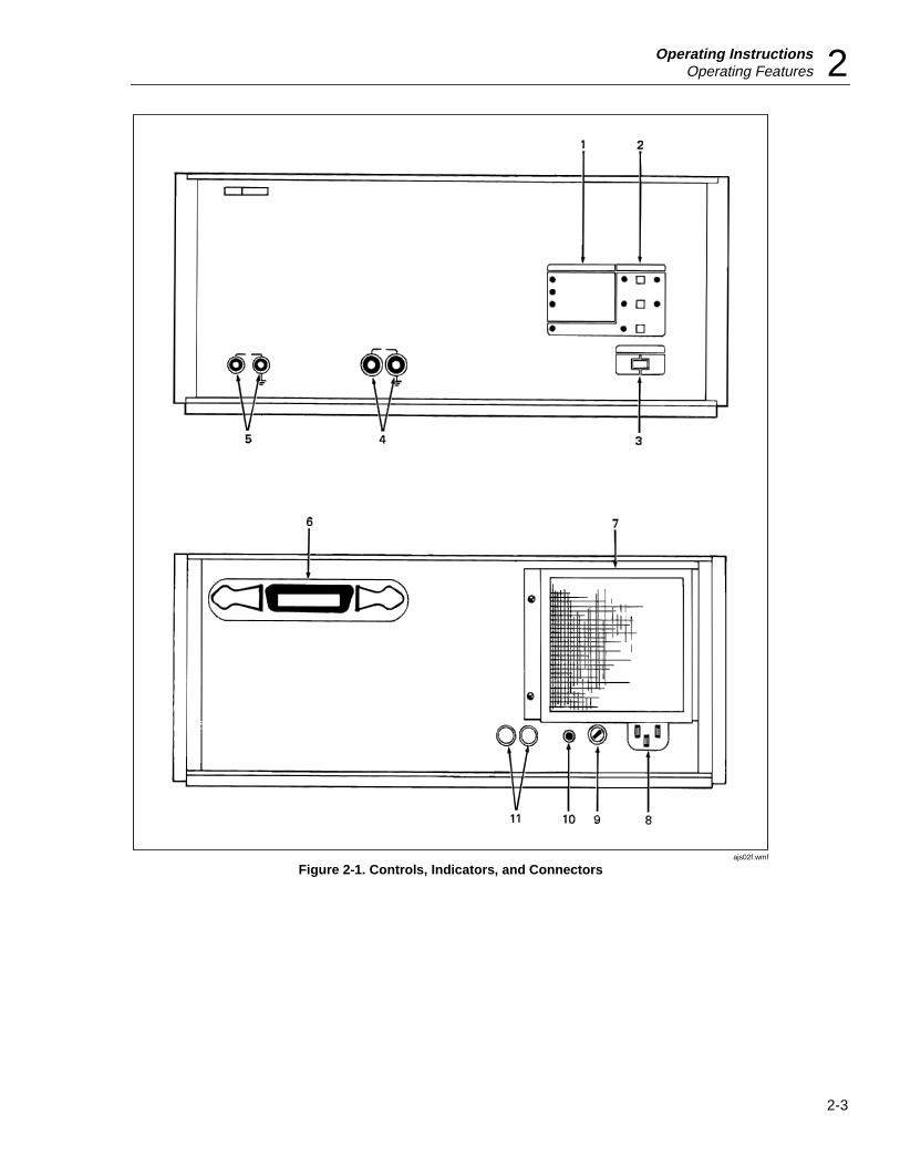
2-8. Operating FeaturesThe function and location of all 5220A controls, indicators, and connectors are shown inFigure 2-1 and described in Table 2-1.
Operating InstructionsOperating Features 2
2-3
ajs02f.wmf
Figure 2-1. Controls, Indicators, and Connectors
5 220AInstruction Manual
2-4
Table 2-1. Controls, Indicators, and Connectors
Ref.No Name Function
1 STATUS Indicators Three LEDs that light on an individual basis to indicate that the 5220Ahas exceeded an operating limit. When the limit condition is detected the5220A is switched to the standby mode. When the limit condition iscleared the LED will remain lit until the 5220A is commanded to theoperate mode. The three status conditions are as follows:
THERMAL CUTOFF: Indicates that the output stage of the 5220A hasexceeded its maximum operating temperature.
OVERCOMPLIANCE: Indicates that the compliance voltage at the outputterminals has exceeded its limit.
OVERCURRENT: Indicates that the output current has beenprogrammed beyond its upper limit.
2 CONTROL Switchesand Indicators
A series of pushbutton switches and LEDs used to select and indicatethe 5220A operating mode. The function of each is as follows:
OPR/STDBY Switch: Allows alternate selection of the standby andoperate modes.
INPUT Switch: Allows alternate selection of the front and rear inputconnectors.
REMOTE Switch: Allows recall of the local mode when remote isenabled and the LOCAL LOCKOUT LED is not lit.
OPR/STBY LEDs: One of the two is lit to indicate the current operatingmode, operate or standby.
FRONT/REAR LEDs: One is lit to indicate the selected voltage inputconnector, front or rear.
REMOTE LED: Lights to indicate that the remote mode has beenremotely selected. If the LED is not lit the local mode is enabled.
LOCAL LOCKOUT LED: Lights to indicate that the unit has beenremotely locked in the remote mode. In this event, the three front panelCONTROL switches are disabled.
3 POWER Switch A push-push switch used to switch instrument power on and off.
4 CURRENT OUTPUTTerminals (Front)
A pair of banana-jack terminals used to provide front-panel connection tothe output of he current source. The terminals are inactive when the rear-panel output terminals are selected.
5 VOLTAGE INGUTTerminals (Front)
A pair of banana-jack terminals that serve as control voltage inputconnections in the local/front-input mode.
6 MIS* Bus Connector A 24-pin connector used as an I/O port for remote operation (Fluke MISBus) of the 5220A. When the 5220A is interfaced with a 5100 SeriesCalibrator (by way of a Y5000 interface) the 5220A output can becontrolled from the 5100 front panel.
7 Ventilation Filter Prevents dirt and debris from being drawn into the 5220A intakeventilation port.
Operating InstructionsOperating Notes 2
2-5
Table 2-1. Controls, Indicators, and Connectors (cont.)
Ref.No Name Function
8 Power Connector Provides the means of connecting the 5220A to ac line power by way ofa 3-wire power cord.
9 Fuse Holder Houses the ac line fuse and allows easy access for fuse replacement.
10 Ground Connector A binding post positioned to provide a convenient connection to chassisground.
11 Current OutputTerminals (Rear)
A pair of banana-jack terminals used as rear-panel current outputconnections. The terminals are inactive when the front-panel CURRENTOUTPUT terminals are selected.
2-9. Operating NotesThe following paragraphs describe the various conditions that should be consideredbefore operating the 5220A.
2-10. AC Line ConnectionThe rear-panel three-prong, U-ground connector permits the 5220A to be connected,through a power cord to 50 or 60 Hz line power. The offset prong on this connector isconnected to the 5220A chassis and should be connected, via the power cord, to a high-quality earth ground.
2-11. Transconductance AmplifierA transconductance amplifier is a current source whose output current level isproportional to an analog input voltage. Electrically, the output of the unit appears as aconstant current source with an output impedance that is much greater than the loadresistance. Similarly, its input impedance is much greater than that of the input voltagesource.
The input/output ratio of the 5220A is 1:1, and the output current range is +20 to –20 A.Therefore, the range of the input control voltage is +20 to –20 V dc. The compliancevoltage of the 5220A is 3 V rms ac or +4 V dc.
2-12. Input Voltage RequirementsInput control voltage for the 5220A can be supplied by any low-impedance voltagesource with an output proportional to the desired output current. The source may be eitherac (30 Hz to 1 kHz) or dc, fixed or adjustable, depending upon the output requirements.
The control voltage source may be connected to either the front-panel VOLTAGEINPUT terminals or the rear-panel voltage input terminals (Pins 5 (low) and 6 (high) ofthe 24-pin connector), but not both simultaneously. Instrument damage will not resultfrom the simultaneous connection of two sources. However, interaction between the twoinputs can result in source loading, which in turn can cause inaccuracy in the expectedcurrent output level.
If a rear-panel input is desirable, the use of the 5100 Series Calibrator and a Y5000Interface is recommended. This combination allows the 5220A to be operated remotelyas an extension of the 5100. If the use of an alternate rear-input source is desirable, theuser is responsible for the proper interface. Details for custom interface requirements canbe derived from the theory of operation (Section 3) and the detailed schematics (Section8).

5 220AInstruction Manual
2-6
2-13. Input Voltage Selection, Front/RearSelection of the front or rear terminals for control voltage input is manually accomplishedby pressing the INPUT push button switch on the front panel. Each depression alternatelyselects front or rear as indicated by the lit FRONT/REAR LED indicator. This switch isactive in the local mode, and inactive in the remote mode.
2-14. Current Output, Front/RearThe 5220A current output can be taken from either a front- or rear-panel set of five-waybinding post terminals, but not both simultaneously. An internal jumper configurationallows qualified personnel to establish the desired output. A detailed output selectionprocedure is given in Section 4, Maintenance.
2-15. Standby/OperateWhen the 5220A is energized it can be placed into one-of-two operating modes; standbyor operate. The enabled mode is indicated by a lit front panel LED; OPR (operate) orSTDBY (standby). Standby is essentially a reset state, in which the output of thetransconductance amplifier is forced to zero regardless of the input control voltage level.In the standby mode both the amplifier and the device connected to its output areprotected from accidental overloads. The operate mode is enabled when an output isrequired. It causes the amplifier to respond to the control voltage input, and therebyprovides the appropriate current level output.
A front panel pushbutton switch (located between the OPR/STDBY LEDs) allowsmanual selection of either mode when the LOCAL LOCKOUT LED is not lit. However,the selection can be counteracted under certain conditions. For example, either mode maybe remotely selected, and the detection of an output overload will command the standbymode. Similarly, when the unit is initially energized it is forced to standby.
2-16. Local/RemoteThe 5220A can be operated manually using the front panel controls, or remotely by wayof the rear panel connector. When the unit is initially energized, it is forced to the localcontrol mode (REMOTE LED is not lit). The remote mode can only be selected by wayof a remote control source. When remote is enabled (REMOTE LED is lit) the localmode can be recalled by a remote command or by pressing the LOCAL push-buttonswitch on the front panel. However, if the LOCAL LOCKOUT is lit (this is also a remotecommand) the local mode can only be recalled by a remote command.
2-17. Status IndicatorsA series of three front-panel STATUS LEDs provide a visual indication of overloadconditions that have been detected at the 5220A output. They are: THERMAL CUTOFF,OVERCOMPLIANCE, and OVERCURRENT. When any one of these conditions isdetected the appropriate LED is lit and the unit is commanded to standby. The LED willremain lit even after the overload condition has been relieved. To return the unit to theoperate mode the overload must be cleared and the operate mode must be commanded. Ifoperate is commanded while the overload is still present, the unit will remain in standby.
A thermal cutoff indication identifies overheating of the current output stage. If theheating is excessive a cooling-down period may be required before the condition iscleared.
The presence of an open-circuit or a high impedance load at the output terminals willcause an overcompliance indication. In this case, an appropriate load will have to be
Operating InstructionsOperating Notes 2
2-7
connected to the output before the condition can be cleared. Overcompliance is detectedas an output voltage outside the range of +4 V dc or 3 V rms ac.
Output current in excess of 20 A will cause an overcurrent indication. To correct thecondition, the input control voltage must be reduced to an acceptable level.
2-18. Audible OutputWhen the 5220A is used to output high current at high frequencies (above 10 A and 1kHz) it may emit an audible tone. The sound is normal and is characteristic of powertransistors that are operated at high current density. Several factors will cause the soundto be more or less apparent. They include background noise, location of the 5220Arelative to the operator, and operator’s hearing ability.
2-19. Inductive LoadsThe 5220A will drive an inductive load of up to 200 µH. However, reasonable care mustbe exercised to ensure the desired results. One or more of the following considerationsmay apply to a given application:
1. Compliance voltage (3.0 V maximum) places a restriction on the product ofinductance and operating frequency for a given output current. This is illustrated inFigure 2-2 for maximum load inductance vs frequency at output currents of 5, 10,and 20 A.
2. A step change in output current into an inductive load can easily produce anovercompliance condition. If the control voltage is being input at the front panelterminals, the rate of change must be controlled to avoid an overcompliance trip. Analternate approach is to set the 5220A to standby before making a change in thecontrol voltage, then select the operate mode. This allows the 5220A to internallycontrol the rate of change. If the control voltage is taken from a Fluke Model 5100Series Calibrator, the calibrator will limit its output to an acceptable rate of change.
3. The leads used to connect a load to the 5220A can add appreciably to loadinductance. For example, a pair of 5-foot leads (10 feet of wire) made of 18 gaugewire (AWG) will have a calculated inductance of 3.86 µH. This is enough to cause anovercompliance trip if a step change in the input control voltage occurs.
4. When driving an ac current through an inductive load the 5220A will exhibitincreased distortion and transconductance error. This is due to a reduction in loopgain caused by the inductance. The graph in Figure 2-3 illustrates the typicaltransconductance error, as a function of frequency, for two different inductive loadvalues.

5 220AInstruction Manual
2-8
ajs03f.wmf
Figure 2-2. Maximum Load Inductance vs Frequency

Operating InstructionsOperation 2
2-9
ajs04f.wmf
Figure 2-3. Typical Transconductance Error for Inductive Loads
2-20. OperationThe following procedure is suggested for operating the 5220A. With reference to theprevious paragraphs proceed as follows:
1. Connect the 5220A to the 5100 Series Calibrator via the Y5000 Interface if remoteoperation is desired. See the 5100B/Y5000 Instruction Manuals for details.
2. Connect the 5220A to line power.
3. Turn-on the 5220A by depressing the POWER switch to the ON position. Only theSTDBY and FRONT indicators should be lit.
4. Energize peripheral equipment as required.
5. If local operation is required, connect the control voltage source to the front-panelVOLTAGE INPUT terminals.
6. Adjust the output of the control voltage source (remote or local) to approximately1 V.

5 2 20AInstruction Manual
2-10
7. Determine the active output terminals (front or rear) by connecting a short jumperwire between the front-panel CURRENT OUTPUT terminals and then pressing theOPR/STDBY switch. If the OVERCOMPLIANCE LED lights, the rear outputterminals are active. Otherwise, the OPR LED will light indicating that the frontCURRENT OUTPUT terminals are active.
8. Press the STDBY switch and then remove the short from the front output terminals.
9. Connect the intended load between the active output terminals.
10. Adjust the control voltage to the desired level.
11. Command the operate mode. If the OPR LED is lit, the predetermined current level isflowing through the load.
12. Set the unit to standby before disconnecting the load or setting the POWER switch toOFF.

3-1
Section 3Theory of Operation
3-1. Introduction
This section of the manual contains an overall functional description followed by adetailed circuit analysis of the 5220A. Both descriptions are supported by blockdiagrams. Component level descriptions contained in the circuit analysis are referenced tothe detailed schematics in Section 8 of this manual.
3-2. Overall Functional Description
3-3. GeneralThe 5220A is a transconductance amplifier. That is, a current source whose outputcurrent is proportional to an analog input voltage. Electrically viewed at the outputterminals, the 5220A appears as a current source with an output impedance that is verymuch greater than the load resistance. Its input terminals exhibit a similar characteristic;the input impedance is larger than that of the input voltage source.
Functionally, the 5220A, as shown in Figure 3-1, can be divided into two sections, analogand digital. The analog section consists of the power supplies, the transconductanceamplifier, and associated analog control circuitry. The digital section comprises the logicnecessary for overall control, and the interfaces necessary for front panel (local)operation and remote operation by way of the Fluke MIS Bus.
3-4. Analog SectionThe power supply used in the 5220A provides operating voltages for both the analog andthe digital section of the unit. It consists of three separate assemblies: the A2 TransformerAssembly, the A3 Cap Bus, and the A4 Regulator. The Cap Bus and RegulatorAssemblies comprise the output portion of the supply, while the Transformer Assemblyprovides isolated ac power for the power supplies. Regulated supply voltages are afunction of the A4 Regulator. These include +5 V dc and +5 V dc Isolated for the digitalcircuits and +15/-15 V dc for analog circuit operation. Unregulated voltages are afunction of the A3 Cap Bus. The Cap Bus is a high-current, +12/-12 V dc source for the5220A current output.

5 220AInstruction Manual
3-2
ajs05f.wmf
Figure 3-1. 5220A Functional Block Diagram

Theory of OperationOverall Functional Description 3
3-3
The transconductance amplifier is a three-stage, closed-loop amplifier whose feedbacksignal is proportional to the 5220A output (load) current. It consists of the A5 Preamp,the A6 Driver, the A7 Output, and a precision four-terminal shunt. Input voltage to theamplifier is presented, by way of front or rear input terminals, to the A5 Preamp. Thisassembly includes relays for front/rear input selection, precision feedback resistors toestablish overall loop gain, and a high-gain amplifier equipped with on/off control forpower-on/off sequencing and failure control. The output of the A5 Preamp is inputdirectly to the A6 Driver where it is buffered and passed on as a differential input to thehigh-current A7 Output stage. Output current from this stage is returned through theoutput load and a precision current shunt to power supply common (COM 2) of the A3Cap Bus (high-current supply). The voltage drop that occurs across the shunt is sent tothe A5 Preamp as a feedback signal, thus closing the loop.
Overall operation of the transconductance amplifier is illustrated in Figure 3-2. When aninput voltage, EIN, is applied to the amplifier an output current, IOUT, is produced. Thecurrent passes through the series connected load and the precision shunt, RS. Currentpassing through the shunt produces a voltage (IR) drop, EOUT, whose polarity (withrespect to COM 1) is opposite that of the input voltage. This voltage is returned to theamplifier as negative feedback through resistor R2. The values of R1, R2 and RSestablished the 1:1 ratio of input voltage to output current. See equations in Figure 3-2.
The analog control circuit constantly monitors the voltage and current outputs of thetransconductance amplifier and provides overcompliance and overcurrent indications tothe digital section of the 5220A. When an overload condition occurs, the digital sectionresponds by sending shut-down signals to the amplifier by way of the analog controllogic. Control sequencing signals (T1, T2) for amplifier turn-on are also processed by theanalog control circuit.
ajs07f.wmf
Figure 3-2. Transconductance Amplifier Simplified Circuit Diagram

5 220AInstruction Manual
3-4
3-5. Digital SectionThe logic portion of the 5220A controls the sequencing of input relays (front/rear) andother control signals that turn the transconductance amplifier on and off. It also providesdrive commands to light appropriate front panel status LEDs. Inputs to the logic are in theform of local/remote control commands from the front panel switches or the remote MISBus Interface, and overload signals from the analog control circuit.
Local or front panel control of the 5220A is accomplished through a series of front panelpushbutton switches which provide direct inputs to the logic circuit. Control and/or statusresponses to the commands are displayed on the front panel LEDs.
Remote control of the 5220A is enabled by the A11 MIS Bus Interface. The interface isintended for use with a 5100 Series Calibrator equipped with a Y5000 Interface. Controldata (analog and digital) is received at the A11 MIS Bus Interface by way of a connectoron the rear panel of the 5220A. In the remote mode, this data is processed by the interfaceand internally coupled with the analog and digital sections of the 5220A.
3-6. Circuit AnalysisA detailed circuit description of the 5220A is given in the following paragraphs. Thedescription is keyed to the functional blocks defined in Figure 3-1. Each block isdescribed separately and is supported by both a block diagram and a detailed schematicdiagram (see Section 8 for schematics).
3-7. Power SupplyThe power supply, as shown in Figure 3-3, consists of the three major assemblies: A2Transformer, A3 Cap Bus, and A4 Regulator. Its function is to transform line power intofour sets of 5220A operating voltages. Each voltage set is isolated from the other, andthree of the four are regulated. The three regulated voltage sets are +15/-15 V dc,+5 V dc, and +5 V ISO (isolated). The unregulated voltage set is +12/-12 V dc.
The A2 Transformer assembly consists of a series of three line-voltage selectionswitches, a power transformer, and appropriate secondary output fuses. Line power to thetransformer passes through the front panel power switch (S4) and the line voltageselection switches before reaching the two primary windings. The setting of the linevoltage switches (S1) connects the primary windings in either a parallel or a seriesconfiguration. Parallel connection is required for 115 V ac operation and the seriesconnection is used for 230 V ac. Switches S2 and S3 allow selection of alternate primarywinding taps. They allow operation from 100, 110, 115 or 120 V ac line voltages in theparallel configuration, or from 200, 220, 230 or 240 V ac in the series configuration. The115 V ac ventilation fan is permanently connected to one of the primary windings, thusensuring proper operation in either voltage configuration. Fuse protection for the powerline is provided by an external fuse (F1) mounted on the rear panel. Supply overloadprotection for the regulated supplies is provided by secondary-winding fuses F4, F5, F6,and F7 located on the A2 Transformer Assembly.
The A3 Cap Bus is a high-current, unregulated, +12/-12 V dc power supply designed toprovide operating power to the output amplifier. It consists of two fuses, a full-waverectifier, two bleeder resistors, and a bank of filter capacitors. Operating voltage isderived from a high-current center-tapped secondary winding of T1. It enters the A3 CapBus through overload fuses F2 and F3, and is full-wave rectified by diodes CR1 throughCR4 to establish both positive and negative supply voltages. Filter capacitors, C1 throughC8, filter the supply outputs. Bleeder resistors, R2 and R3, discharge the filter capacitorswhen line power is turned off.

Theory of OperationCircuit Analysis 3
3-5
The A4 Regulator is designed to convert the ac outputs from the three remainingsecondary windings of T1 into three sets of isolated and regulated voltages: +5 V dc,+15/-15 V dc, and +5 V dc ISO (isolated). Each voltage is produced using conventionalregulating techniques. That is, it is rectified, filtered, regulated by a three-terminalregulator, and filtered again before being output. A fifth voltage, Line Mon (monitor), isalso produced on the A4 Regulator. It is derived from the T1 windings used for the+15/-15 V dc supply and is used to convey the line power status of the 5220A to the A10Logic. The voltage is rectified by diodes CR8 and CR9, and clipped by zener VR1 beforebeing output.
ajs08f.wmf
Figure 3-3. Power Supply Functional Block Diagram

5 220AInstruction Manual
3-6
3-8. PreamplifierThe A5 Preamplifier, as shown in Figure 3-4, is a high-gain amplifier designed to accepta front/rear panel input signal and provide an amplified output to the A6 Driver stage ofthe transconductance amplifier. It consists of a high-gain differential amplifier withfeedback resistors, front/rear input select relays, and turn-on/off control circuitry.
In operation, the input voltage source (front or rear), as selected by the A10 Logic, isconnected through reed relay K1 (front) or K2 (rear) and input resistors R1, R3, and R13to the inverting input of a differential transistor pair, Q2. The non-inverting input of Q2 isconnected to COM 1 through parallel resistors R9 and R14. The resistance valueapproximates the value of R1 and R2 in parallel and, thereby balances the sourceimpedance at the amplifier inputs. Balance is required to minimize apparent input offsetvoltage that may result from input currents. Diode CR3 and diode-connected transistorQ3 are voltage clamps that prevent amplifier saturation on high input transients. Thecollectors of Q2A and Q2B drive the emitters of a pair of grounded base amplifiersformed by transistor array, U1. This holds the collectors of Q2 at a low and equal level tomaintain low and equal collector-to-base leakage currents (ICER) at Q2. The actualcollector voltage of Q2 is set by the temperature corrected divider formed by R4, R19,and the diode connected transistor U1C. Voltage variations at the collectors of U1A andU1B constitute the output of the differential amplifier, and are used as the input to op-amp, U2. Diodes CR4 and CR5 clamp the inputs to prevent U2 saturation when transientvoltages appear. An ac feedback network, R15 and C7, fix the frequency response of thepreamplifier to satisfy the overall transconductance amplifier loop. Amplifier zero isestablished by the selected values of collector resistors R11 and R12, and the setting ofthe zero-adjust potentiometer, R6.
ajs09f.wmf
Figure 3-4. A5 Preamplifier Functional Block Diagram
The turn-on/off control FET (Q1) operates as FET switch to control the overall gain ofthe A5 Preamplifier in both the standby and operate modes. Q1 responds to the FETDrive 1 signal initiated (as T2) on the A10 Logic.
In the standby mode FET Drive 1 is near zero volts causing Q1 to turn on. FET Q1completes the feedback loop between the output of U2 and the inverting input of Q2. Thisin effect reduces the gain of the A5 Preamplifier to zero. As a result the output of thetransconductance amplifier is forced to zero amperes. Photo resistor U3 is used to control

Theory of OperationCircuit Analysis 3
3-7
the rate at which the input voltage is applied to the A5 Preamplifier when the 5220A isswitched from standby to operate. This is necessary to prevent a step output which, ifapplied to an inductive load, would result in an overvoltage transient, forcing the 5220Aback to standby. In standby both input select relays, K1 and K2, are open, capacitors, C3and C12, are discharged, and the photo resistor U3 is a very high impedance with theLED drive removed. Thus, the A5 Preamplifier is effectively isolated from the inputvoltage.
In the operate mode FET Drive 1 is stepped to –15 V dc causing FET Q1 to turn off.With Q1 off, the A5 Preamplifier returns to its high gain state with feedback establishedby resistors R1 and R2. If front input is selected, the Relay 1 drive signal is low andcapacitor C12 begins charging. The increasing voltage across C12 increased the LEDoutput from U3 which, in turn, decreases the impedance of the photo resistor. Since theresistor is in parallel with the input contacts of the still open front input relay K1, it actsas a variable input attenuator. In other words, the front input voltage is applied to theinput of the A5 Preamplifier at a controlled rate and not as a step input. At the same time,a low Relay 1 drive signal is inverted by U4 causing C3 to charge through R24. When thecharge reaches the threshold of the second inverter (U4) relay K1 is energized by a set offour parallel connected inverters. The charge time for C3 and C12 are designed to ensurethat K1 closes after photo resister U3 changes to a low impedance. When K1 closes, itplaces a short across the resistor in U3 and selects the front panel input voltage to drivethe A5 Preamplifier. If the rear panel input signal is selected, a variable attenuator is notnecessary because the signal from the remote 5100A rises at a controlled rate whenswitched from standby to operate.
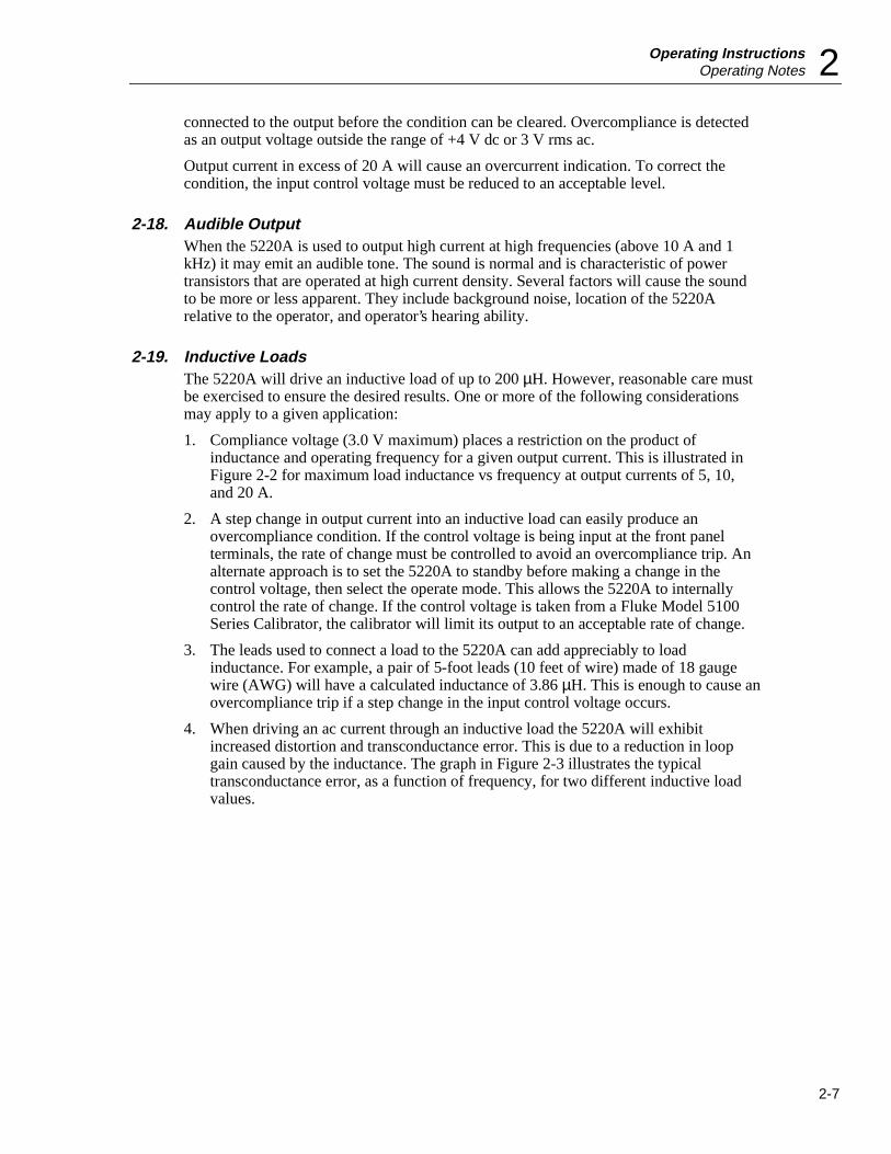
3-9. A6 DriverThe A6 Diver, as shown in Figure 3-5, is a differential amplifier designed to accept itsinput from the A5 Preamplifier and to provide a differential drive signal to the A7 Outputstage. The amplifier itself is of a discrete-component, complementary, push-pull design.Its features include the following:
• Temperature compensated biasing for both itself and the A7 Output stage
• An amplifier-disable circuit for standby operation
• An output-leakage current sink for standby operation.
The input section of the driver amplifier consists of a differential transistor pair, Q2 andQ3; a current regulator, Q4; and a common base driver, Q1, for the bias circuit.Transistor Q3 of the input pair receives the drive input from the A5 Preamplifier. Theother input transistor, Q2, is driven by Shunt Sense 2, which provides negative feedbackfrom the output current shunt to reduce distortion in the A7 Output stage. Currentregulator Q4 regulates the emitter current of the differential pair, and provides isolationfrom variations in the –12 V supply. Output from the differential pair is taken at thecollector of Q3 by way of a common-base driver, Q1.
The bias section of the driver amplifier consists of resistors, R13 through R17, currentregulator, CR1, and transistors, Q5 and Q107 (Q107 is physically located on the outputamplifier's heat sink). Resistors R13 through R17 and current regulator CR1 form a seriesstring that is driven by the output driver Q1 of the input amplifier. Regulator CR1 is atthe end of the string and connected to –12 V dc. This ensures a constant current ofapproximately 5.2 mA through the string. Transistors Q5 and Q107 are connected acrossresistors R14, R15 and R16, R17 as VBE multipliers to ensure that the voltage dropacross the resistor string changes at a rate which will compensate for VBE temperaturechanges in the A6 Driver and A7 Output stages. Transistor Q5 senses ambienttemperature changes while Q107 senses temperature changes due to power dissipation inthe A7 output. The temperature compensated voltage drop developed across the resistor
5 220AInstruction Manual
3-8
string is used as a voltage source to set the quiescent bias for the remaining stages of thecomplementary A7 Driver and A7 Output. Variable resistor R13 is used to set the initialbias voltage.
ajs10f.wmf
Figure 3-5. A6 Driver Functional Block Diagram
The characteristics of the VBE multipliers used in the bias section are stated in terms ofQ5 in the following formulas:
VBE = [R14/R14 + R15] VCE
VCE = VBE [R14 + R15/R14]
The output section of the A6 Driver consists of transistors Q8, Q9, Q10, Q12, andassociated components. Transistors Q8 and Q9 are arranged as complementary emitterfollowers that are both biased and driven by the bias section. This is followed by acommon collector stage using Q10 and Q12. Overcurrent protection is provided in thestage by the 10 ohms resistors, R30 and R31, in the collector circuits. The differentialoutput at the emitters of Q10 and Q12 is used as the drive input to the A7 output stage.
In the standby mode of operation it is necessary to reduce the 5220A output to a zero-volt/zero-current condition. This is accomplished on the A6 Driver by two separate FETcircuits. FETs Q6 and Q7 comprise the voltage shut-down circuit, and FET Q11 is theoutput current-sink. Both are enabled by a Turn-on 1 signal which is initiated (as T1) bythe A10 Logic when the 5220A is switched to standby. When Q6 and Q7 are enabled(turned on) they remove the bias from the output stage of the A6 Driver, and therebydisable the bias to the A7 Output stage. In this state the output is essentially floating andis influenced only by leakage current that may be present in the output drivers. FET Q11remedies the floating condition by effectively clamping the output to output common(COM 2).
Theory of OperationCircuit Analysis 3
3-9
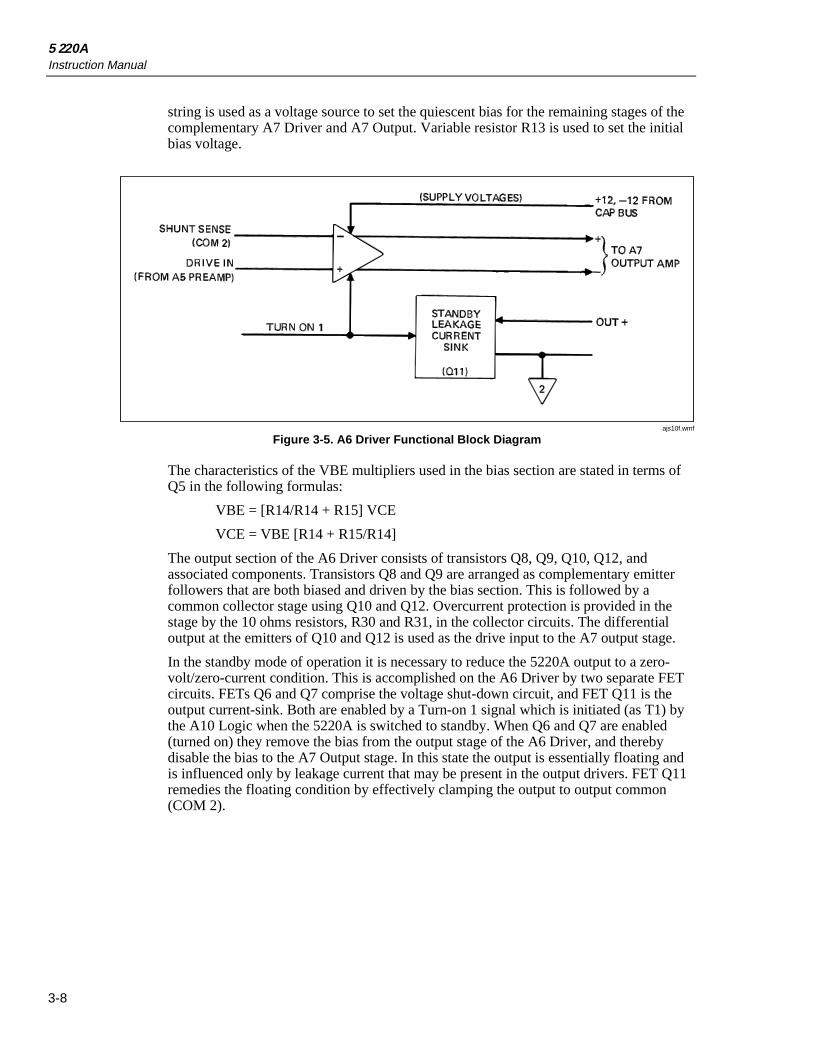
3-10. A7 OutputThe A7 Output is a discrete-component, complementary-output, high-current amplifierwhich serves as the final output stage of the transconductance amplifier. See Figure 3-6.It consists of a pair of driver transistors, Q101 and Q102; two parallel pair(s) of outputtransistors, Q103, Q104 and Q105, Q106; a thermal sensing transistor, Q107; and athermal overload switch S101. The differential output from the A6 Driver is applied tothe bases of Q101 and Q102. These transistors are configured as emitter followers andprovide the high current drive required by the output transistors. Collector resistors, R114and R115, for Q101 and Q102 provide current limit protection under transient or faultconditions. Emitter resistors in the parallel output pairs prevent current hogging whichwould otherwise occur due to unequal VBE characteristics.
ajs11f.wmf
Figure 3-6. A7 Output Functional Block Diagram
All transistors in the A7 Output as well as the thermostatic switch, S101, are physicallymounted on a common heat sink. The temperature of the heat sink is sensed by Q107(part of the A7 Driver’s bias network) and returned to the A7 Driver to provide biascompensation for the change in VBE with output-transistor temperature. (See A7 Driverdescription given earlier in this section of the manual.) Thermostatic switch S101 sensesthe temperature of the heat sink and provides an open contact output when an over-temperature condition is detected. The open output is sent to the A10 Logic which reactsby switching the 5220A to standby (over temperature may result from a loss or restrictionof cooling airflow).

5 220AInstruction Manual
3-10
3-11. A8 Analog ControlThe A8 Analog Control Assembly, as shown in Figure 3-7, contains an overcompliancedetector, an overcurrent detector and two TTL-to-FET level shifters. The detectioncircuits are used to switch the 5220A to standby when an overcurrent or overcompliancecondition occurs. The level shifters are driven by the A10 Logic to control the turn-on/offsequencing of the transconductance amplifier.
ajs12f.wmf
Figure 3-7. A8 Analog Control Simplified Block Diagram
The detection circuits are absolute value level detectors that provide a TTL outputindication of the transconductance amplifier’s operating status; i.e., output voltage statusand output current status. As long as both output voltage and current are within theirspecified operating range, both detectors will output a low logic level as a normal-operation status indication. However, if either or both the specified compliance voltageand/or the output current are exceeded, the appropriate detector will output a high logiclevel. Upon receipt of a high logic level from either detector the A10 Logic switches the5220A to standby.
Each of the detectors is basically the same. They consist of an absolute value amplifier(full-wave rectifier), a level conditioner, a zener diode threshold detector, and a TTLbuffered output stage. The absolute value amplifier is essentially a pair of operationalamplifiers configured to provide an output voltage that is equal to the amplified positiveabsolute value of the input signal. The input to the compliance detector is connected tosense the voltage present at the output terminals (+OUT and COM 1). Similarly, the inputto the overcurrent detector is connected to sense the voltage drop across the current shunt(COM 2 and COM 1). The result, in both cases, is a negative output level that is equal tothe absolute value of the input signal. This level is sent to a level conditioner where it isfiltered/integrated, inverted, and amplified. An adjustable gain control in the levelconditioner’s feedback loop provides for accurate adjustment of the trip level.
The output of the level conditioner feeds a series connected zener/resistor circuit with theresistor connected to logic common (COM 3). When the output of the level conditionerexceeds the zener voltage, the excess is dropped across the zener resistor. This voltage ismonitored by a series-connected-pair of inverters which respond to the voltage drop as if

Theory of OperationCircuit Analysis 3
3-11
it were a logic level. That is, voltages from 0 to an approximate 2 V threshold areconsidered a low logic level. A high logic level is approximately 2 to 4.5 V.
The TTL-to-FET level shifters are used to interface turn on/off commands TTL logiclevels, T1 and T2, from the A10 Logic with the standby/operate control FETs in thetransconductance amplifier. Both level shifters are identical in design. The input isdesigned to respond to voltage levels from +0.01 to +5.0 V dc. Corresponding outputlevels to drive the FET gates are 0 to –15 V dc.
3-12. A9 Front PanelThe A9 Front Panel Assembly contains the switches (with the exception of the powerswitch) and LEDs that comprise the 5220A controls and indicators. The switches are usedto manually convey control information to the A10 Logic. This includes selection of thelocal operating mode, standby/operate, and front/rear panel input. The LEDs display thecurrent operating status of the 5220A as determined by the A10 Logic. Status conditionsinclude: remote, local lockout (LLO), overcompliance, overcurrent, thermal cutout, frontpanel input, rear panel input, standby, and operate.
Electrically, the LEDs (anode end) and the switches (arm) are connected to a common +5V bus powered by the logic supply. A switch depression represents a +5 V output to theA10 Logic. A series resistor connected to the anode end of each LED serves as a currentlimiter when the LED is lit. A low logic level from the A10 Logic lights the appropriateLEDs.
3-13. A10 LogicThe A10 Logic, as shown in Figure 3-8, is designed to process and control the timing andthe input/output of all 5220A digital control data. Input data is received from the frontpanel controls, the A11 MIS Bus Interface, and the analog protection circuits of thetransconductance amplifier. Output data provides timing and control signals to theamplifier (including its relays) and the front panel indicator LEDs.
3-14. Reset LogicThe reset logic consists of dual multivibrator U11, RC network R7/C2, or gate U9-10,and inverter U3-10. Its function is to command the reset of the A10 Logic, and thus the5220A, to an initial state when any one of the following events occur:
1. The 5220A is initially energized.
2. The +15/-15 V dc power supply is interrupted.
3. Control is switched from remote to local.
When the 5220A is energized the +5 V dc power supply rapidly rises to its +5 V level tosupply operating voltage to the A10 Logic Assembly. The voltage rise is integrated byRC network R7, C2. The slow rising voltage across C2 is used as a momentary low logiclevel to issue a reset command to all sections of the A10 Logic. Some sections are resetdirectly by the voltage across C2 while others are reset indirectly by the response of U11-10 to the voltage across C2.

5 220AInstruction Manual
3-12
ajs13f.wmf
Figure 3-8. A10 Logic Simplified Block Diagram
Loss or interruption of the +15/-15 V dc supply output causes the Line Mon (monitor)input from the power supply to go low. Normally, the line monitor input is a clipped full-wave rectified 60 Hz waveform which is generated on the A4 Regulator Assembly. Thenegative-going edge is used as the trigger for monostable U11-7 which is timed toprovide an output pulse of approximately 0.1 second. Since the output is longer than thetime between triggers, it will remain active (Q low) as long as the Line Mon (monitor)

Theory of OperationCircuit Analysis 3
3-13
input is present. Under normal operating condition the reset command is high at U9-10and low at U3-10.
When the 5220A is switched from remote to local operation the local/remote logictriggers monostable U11-10 in the reset logic circuit. The result is a momentary positive-going pulse at the Q output of U11-10. This in turn drives the complementary reset linesof U9-10 and U3-10.
The overall result of a reset command, regardless of how it is initiated, is to set the outputcommands of the A10 Logic to the states shown in Table 3-1. Essentially the unit iscommanded to standby operation with front panel inputs selected. Remote and LocalLockout (LLO) commands are not affected by the reset command.
Table 3-1. Effect of Reset Command on A10 Logic and A9 Front Panel
Signal Name Logic State Front Panel LED Status
Interface Operate Status Low None
Operate LED High OPER LED off
Standby LED Low STDBY LED on
T1, T2, and T4 Low None
Relay 1 High None
Relay 2 High None
Front Panel Input LED Low FRONT LED on
Rear Panel Input LED High FRONT LED OFF
Overcompliance LED High OVERCOMPLIANCE LED off
Overcurrent LED High OVERCURRENT LED off
Thermal Cutout LED High THERMAL CUTOFF LED off
Interface Overload Status Low None
3-15. Timing LogicThe timing logic controls the timing sequence used to switch the transconductanceamplifier between the standby and operate modes. It consists of a bi-directional shiftregister U22, D-type flip-flops U17-1, and free running multivibrator U23. Themultivibrator runs at a frequency of 100 Hz (10 ms period) and serves as the clock forboth the flip-flop and the shift register. Flip-flop U17-1 responds to the Reset command(reset input) and the standby/operate commands (D-input) to select the shift register’scontrol mode; i.e., shift left or shift right. The shift register’s four outputs are sequencedlow in the shift-left mode and high in the shift-right mode. With all outputs low thetransconductance amplifier is set to standby. The amplifier is operational when all outputare high.
The shift-left mode is selected when flip-flop U17-1 drives the register’s S0 input low andits S1 input high. (This occurs as the result of a standby or reset command.) In this modethe register sequentially propagates the low input at U22-7 through the register causingits four outputs (QA, QB, QC, and QD) to be sequentially driven low. Since the registershifts at the rate of the 100 Hz clock, the outputs are sequenced at intervals of 10 ms. Atthe end of four clock pulses all four outputs are low (standby), and will remain low untilthe register is commanded to shift right.

5 220AInstruction Manual
3-14
The shift-right mode is selected when flop-flop U17-1 responds to an operate command(D-input low) and drives the register’s S0 input high and the S1 input low. This results inthe high input at U22-2 being sequentially propagated through the register and its fouroutputs (QD, QC, QB and QA) being driven high (operate).
The outputs of the shift register are used as control signals to sequence the turn-on andturn-off of the transconductance amplifier. They are designated T1, T2, and T4 (T3 is notused) and their sequence is shown in Figure 3-9. The control function of each of thesignals is as follows:
1. T1 turns the A6 Driver on and off.
2. T2 turns the A5 Preamplifier on and off.
3. T4 enables/disables the selected front/rear input relay (K1 or K2) on the A5preamplifier.
ajs14f.wmf
Figure 3-9. Timing Sequence
3-16. Standby/Operate LogicThe standby/operate logic consists of optical isolators U1 and U5, monostable U8-7, D-type flip-flop U10-9, and a series of supporting logic gates and buffers. Its function istwofold. One, it responds to reset and external inputs to command the state of the timinglogic, shift left (standby mode) or shift right (operate). Two, it drives the front-panelSTANDBY/OPERATE LEDs and provides the A11 MIS Bus Interface (remote interface)with an Interface Operate Status (Standby/Operate) signal. Flip-flop U10-9 is used tostore the commanded mode (standby or operate) and to provide the necessary commandsto the shift register (in the timing logic) and the LED/status drivers. Optical isolators U1and U5 are used to electrically isolate remote control signals to and from the A11 MISBus Interface from the A10 Logic.
Standby/operate commands occur in the form of Reset, Standby/Operate, not Operate,Sw(itch) 1, Overcompliance, and Overcurrent. Reset is an onboard command from thereset logic. It sets the 5220A to standby by commanding U10-9 to the clear state (Q low).Standby/Operate is received in the form of a +5 V (high) input each time the front-panelSTANDBY/OPERATE switch is pressed. If the 5220A is in the local control mode, eachpress of the switch will clock flip-flop U10-9 to its alternate state. The result is analternate selection of either the standby or the operate mode, as indicated by the front-panel STANDBY and OPERATE LEDs. A similar command, Interface Operate Status(also derived from the state of U10-9), is issued to the A11 MIS Bus Interface; low
Theory of OperationCircuit Analysis 3
3-15
indicates standby, high indicates operate. The not Operate signal is received from theA11 MIS Bus Interface and is effective only when the 5220A is in the remote controlmode. In the high state, the signal clears flip-flop U10-9 to invoke the standby mode.When not Operate goes low it presets flip-flop U10-9 (by way of U8-7) to invoke theoperate mode. Overload signals received at the standby/operate logic include; ThermalSw(itch) 1, Overcompliance and Overcurrent. When any one of these signals goes high,flip-flop u10-9 is cleared to the standby state.
3-17. Local/Remote LogicThe local/remote logic consists of optical isolators U4 and U20-8, monostable U8-9,D-type flip-flop U7, and a series of supporting logic gates and buffers. Its function is toenable selection of the desired control mode (local or remote) and to provide the drive forthe appropriate front panel and A11 MIS Bus Interface status indicators. These includeLLO (Local Lock Out) LED, Remote LED, and Interface Remote Status. Flip-flop U7 isused to store the commanded mode (local or remote) and to provide the necessarycommands to the onboard logic and the LED/status drivers. Optical isolators U4 andU20-8 electrically isolate remote control signals to and from the A11 MIS Bus Interfacefrom the A10 Logic.
Local/remote commands are received in the form of Local, not Remote, and not LLO(Local Lockout). Local occurs as a momentary +5 V (high) input each time the frontpanel LOCAL switch is pressed. If the 5220A is in the remote control mode and LocalLockout is not commanded (high) pressing the front panel LOCAL switch will initiate a 1µs pulse from monostable U8-9. This pulse clears flip-flop U7, which in turn, commandsthe A10 Logic to the local mode (Rem Stat low). As a result, the Remote LED and LLOLED signals are high, Interface Remote Status is low. However, if not LLO is low whenthe LOCAL switch is pressed, monostable U8-9 will be held in the reset state and flip-flop U7 will not be cleared. Thus, the A10 Logic is effectively locked into the remotemode until not LLO is returned high.
The not Remote signal is received from the A11 MIS Bus Interface and is used toremotely command the A10 Logic to the remote control mode. When the signal goes lowit is coupled across optical isolator U4 to the clock input of D-type flip-flop U7. This setsthe Q Output of U7 high to select the remote control mode (Rem Stat high). As a result,the Remote LED signal goes low to light the REMOTE LED and the Interface RemoteStatus output goes high.
When the 5220A is commanded to the remote mode the front-panelSTANDBY/OPERATE and FRONT/REAR switches are disabled and the correspondingremote inputs are enabled. Similarly, if LLO is remotely enabled, the LOCAL pushbuttonis disable.
3-18. Front/Rear Input LogicThe front/rear input logic is used to command the front/rear input relays on the A5Preamplifier and to drive the appropriate FRONT/REAR LED on the front panel. Whenthe A10 Logic is in the local mode, Front/Rear commands are received from the frontpanel pushbutton. Each switch depression is received as a +5 V (high) level that is usedto clock alternate states on D-type flip-flop U10-5. The FRONT LED and Relay K1 arecommanded when the Q output of U10-5 is low. When the A10 Logic is in the remotemode the not Rear input signal is used to command the front/rear input relays. Front inputis selected when not Rear is high. Actual opening/closing of the relays is enabled at timeT4 of the timing logic.

5 220AInstruction Manual
3-16
3-19. Failure Status LogicThe failure status logic consists of three D-type flip-flop (U16-1, U16-13, and U17-13)and their associated logic gates and drivers. Its function is to store failure conditionsdetected by other parts of the A10 Logic and to drive the front panel STATUS indicators.An optical isolator is also included for providing an Interface Overload Status signal tothe A11 MIS Bus Interface. Front panel status indicators comprise three LEDs:OVERCOMPLIANCE, OVERCURRENT, and THERMAL CUTOUT. When any one ofthese LEDs is lit, Interface Overload Status is driven high.
The inputs to the D-type flip-flop are connected to respond to three commands: reset,clock, and set. The reset and clock inputs are used to set the Q outputs low, and therebyremove the drive from the front panel STATUS LEDs. The three reset inputs areconnected in parallel and are commanded when the 5220A is initially energized andwhen it is remotely commanded from standby to operate. The clock inputs are alsoconnected in parallel. They respond to a high input that transfers the low D-input to the Qoutput. The clock is driven high under the following conditions:
1. When the STDBY/OPR pushbutton is pressed.
2. When the FRONT/REAR pushbutton is pressed.
3. When an onboard reset is initiated.
The set-inputs to the flip-flops in the failure status logic are used to set the Q outputs highwhen a failure status is detected. This causes the corresponding STATUS LED to be litand the Interface Overload Status signal to go high. Each flip-flop responds to one of thefailure signals issued by the transconductance amplifier. They are:
1. Thermal Sw(itch) 1
2. Overcompliance
3. Overcurrent
3-20. A11 MIS Bus InterfaceThe A11 MIS Bus Interface, as shown in Figure 3-10, is a remote control interface thatallows the 5220A to operate as an extension of a 5100 Series Calibrator equipped with aModel Y5000 Interface. An accessory cable is available for use with the Y5000 tocomplete the necessary connections between the Y5000 and the A11 MIS Bus Interface.
Functionally, the A11 MIS Bus Interface (hereafter referred to as the MIS I/F) performsthree basic functions: receives and stores digital control data from a remote controlsource (Y5000), interfaces 5220A status signals to the Y5000, and provides a connectingpath between the remote analog input signal (Aux Out) and the rear-input connections onthe A5 Preamplifier. Operating power for the assembly is derived from the +5 V ISO(isolated) power supply.
Control data is received at the MIS I/F via the data bus as a 4-bit parallel word. When the5100 Series Calibrator places the correct address on the address bus (BC0, BC3, and BC6high), the write data logic responds by pulling the not ACK (acknowledge) line low andclocking the control data word into the data register, U1. The not ACK signal is sent tothe 5100 to acknowledge the receipt of a valid address. The register outputs are bufferedand inverted by U6 before being used as remote programming inputs to the A10 LogicPCB (i.e., not Remote, not Operate, not LLO and not Rear). At the same time that theaddress is acknowledged, an RS flip-flop in the write data logic is set.
The function of the RS flip-flop is to prevent two successive status read inputs to the5220A. The flip-flop is set when a high is present on inputs BC0, BC3, and BC6. Thisresults in a low output from U5-8 and a high output from U4-6. In this state gate U5-8 is
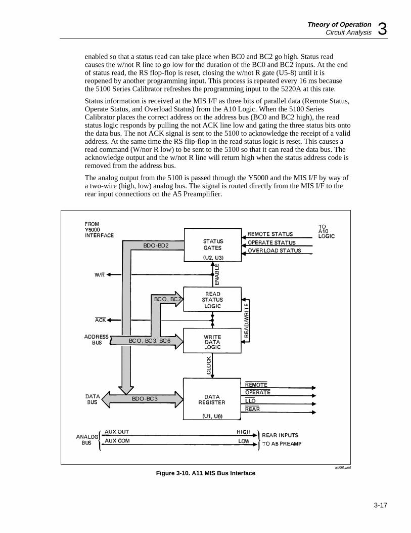
Theory of OperationCircuit Analysis 3
3-17
enabled so that a status read can take place when BC0 and BC2 go high. Status readcauses the w/not R line to go low for the duration of the BC0 and BC2 inputs. At the endof status read, the RS flop-flop is reset, closing the w/not R gate (U5-8) until it isreopened by another programming input. This process is repeated every 16 ms becausethe 5100 Series Calibrator refreshes the programming input to the 5220A at this rate.
Status information is received at the MIS I/F as three bits of parallel data (Remote Status,Operate Status, and Overload Status) from the A10 Logic. When the 5100 SeriesCalibrator places the correct address on the address bus (BC0 and BC2 high), the readstatus logic responds by pulling the not ACK line low and gating the three status bits ontothe data bus. The not ACK signal is sent to the 5100 to acknowledge the receipt of a validaddress. At the same time the RS flip-flop in the read status logic is reset. This causes aread command (W/nor R low) to be sent to the 5100 so that it can read the data bus. Theacknowledge output and the w/not R line will return high when the status address code isremoved from the address bus.
The analog output from the 5100 is passed through the Y5000 and the MIS I/F by way ofa two-wire (high, low) analog bus. The signal is routed directly from the MIS I/F to therear input connections on the A5 Preamplifier.
BDO-BD2
BCO, BC2
BCO, BC3, BC6
BDO-BC3
ajs06f.wmf
Figure 3-10. A11 MIS Bus Interface

5 220AInstruction Manual
3-18
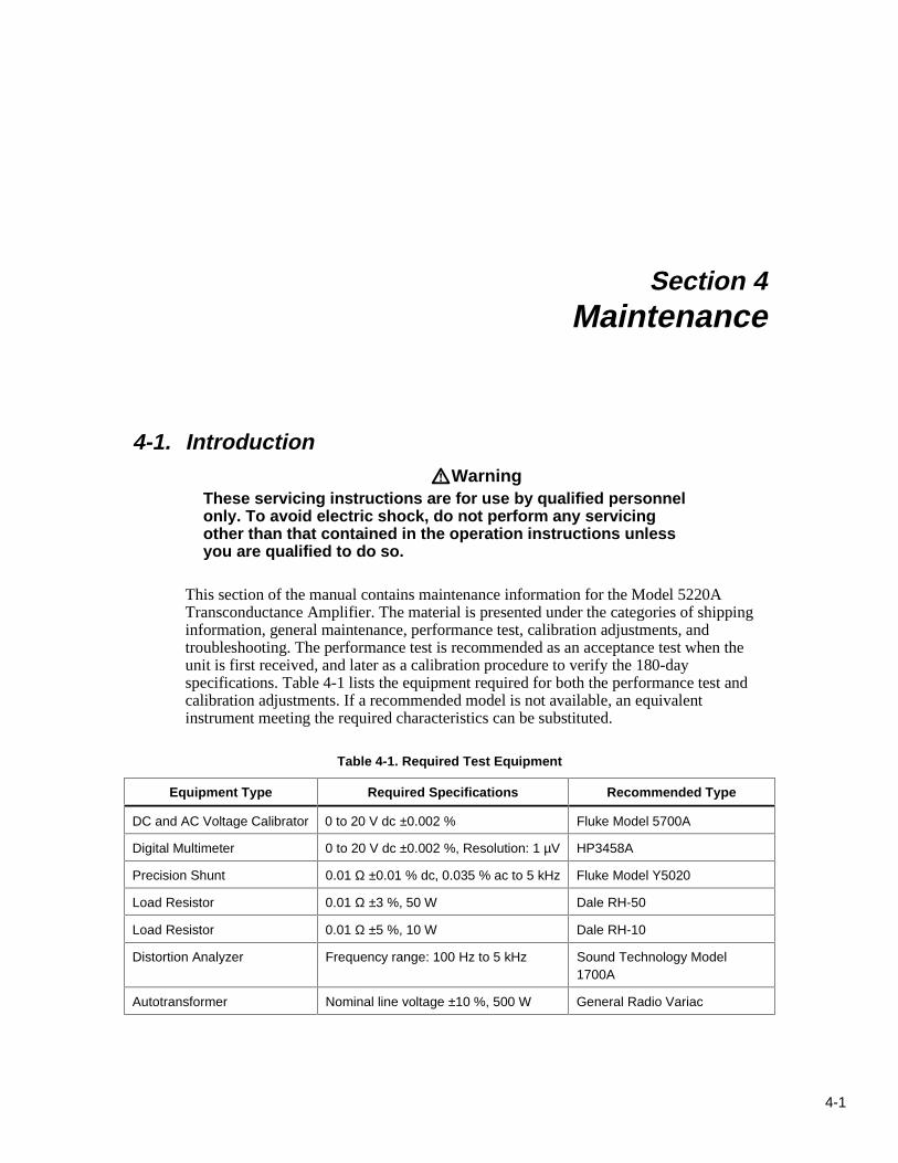
4-1
Section 4Maintenance
4-1. IntroductionWWarning
These servicing instructions are for use by qualified personnelonly. To avoid electric shock, do not perform any servicingother than that contained in the operation instructions unlessyou are qualified to do so.
This section of the manual contains maintenance information for the Model 5220ATransconductance Amplifier. The material is presented under the categories of shippinginformation, general maintenance, performance test, calibration adjustments, andtroubleshooting. The performance test is recommended as an acceptance test when theunit is first received, and later as a calibration procedure to verify the 180-dayspecifications. Table 4-1 lists the equipment required for both the performance test andcalibration adjustments. If a recommended model is not available, an equivalentinstrument meeting the required characteristics can be substituted.
Table 4-1. Required Test Equipment
Equipment Type Required Specifications Recommended Type
DC and AC Voltage Calibrator 0 to 20 V dc ±0.002 % Fluke Model 5700A
Digital Multimeter 0 to 20 V dc ±0.002 %, Resolution: 1 µV HP3458A
Precision Shunt 0.01 Ω ±0.01 % dc, 0.035 % ac to 5 kHz Fluke Model Y5020
Load Resistor 0.01 Ω ±3 %, 50 W Dale RH-50
Load Resistor 0.01 Ω ±5 %, 10 W Dale RH-10
Distortion Analyzer Frequency range: 100 Hz to 5 kHz Sound Technology Model1700A
Autotransformer Nominal line voltage ±10 %, 500 W General Radio Variac

5 220AInstruction Manual
4-2
4-2. Service InformationThe 5220A is warranted for a period of 1-year upon delivery to the original purchaser.The warranty is located on the back of the title page.
Factory authorized calibration and service for each Fluke product is available at variousworldwide locations. A complete list of these service centers is included in Section 7 ofthis manual. If requested, an estimate will be provided to the customer before work isbegun on instruments that are beyond the warranty period.
4-3. General Maintenance
4-4. CleaningClean the 5220A periodically to remove dust, grease, and other contamination. Use thefollowing procedure:
1. Clean the front panel and case with a soft cloth dampened with a mild solution ofdetergent and water.
2. Clean the surface of the PCBs using clean, dry air at low pressure (<20 psi). If greaseis encountered, spray with Freon T.F. Degreaser and remove grime with dry, low-pressure air.
4-5. Air Filter MaintenancePeriodically inspect the air filter on the rear panel for dirt and contaminants. If cleaning isrequired, use the following procedure:
1. Disconnect the 5220A from line power.
2. Remove the two screws from the filter housing and gently pull the filter assemblyfrom the unit.
3. Clean the filter using either low-pressure air or a mild solution of detergent andwater.
4. Dry (if necessary) and reinstall the filter.
4-6. Access InformationThe 5220A is a modular instrument that can be easily disassembled by sections.Procedures for section disassembly are given in the following paragraphs. Someprocedures require the completion of previous procedures in the disassembly process.When this occurs, the previous procedure will be referenced, but not repeated.
WWarningTo avoid electrical shock hazard, disconnect he 5220A from linepower before attempting any of the following disassemblyprocedures.
Reassembly of the instrument is accomplished by logically reversing the disassemblyprocedure. Before installing the top covers on the unit, make a visual comparison withFigure 4-1 to ensure the presence of all assemblies, jumpers, and fuses.

MaintenanceGeneral Maintenance 4
4-3
ajs15f.wmf
Figure 4-1. Internal Component/Assembly Locations
CautionTo prevent component damage observe static awarenessprecautions during instrument disassembly/assembly. Refer tothe yellow insert sheet following Section 1.
5 220AInstruction Manual
4-4
4-7. Internal Components/AssembliesAll internal switches, fuses, and calibration adjustments can be accessed by removing thetop cover and the large inner cover from the 5220A. The location of each of theapplicable components is shown in Figure 4-1. Procedures for setting, replacing, and/oradjusting these components are given later in this section of the manual.
4-8. Front Panel RemovalThere are no electrical components physically mounted on the front panel of the 5220A.Use the following procedure to remove the front panel:
1. Remove the top and bottom covers from the 5220A.
2. Stand the instrument on its rear handles. Use a solid work surface.
3. Locate the two tabs at the rear of each front handle and remove the tab screws (4total).
4. Lift the front panel from the chassis.
4-9. A9 Front Panel PCB RemovalUse the following procedure to access and remove the A9 Front Panel PCB Assembly:
1. Remove the front panel.
2. Remove the two screws from the top of the A9 Front Panel PCB Assembly.
3. Pull the PCB from its connector (J10).
4-10. A2 Transformer Assembly RemovalUse the following procedure to remove the A2 Transformer Assembly from the 5220A:
1. Remove the top cover from the 5220A.
2. Remove the large inner cover.
3. Locate and remove the two screws that hold the A2 Transformer Assembly to thechassis side.
4. Remove the two screws that hold the A2 Transformer Assembly to the Motherboard.These screws are located on the bottom right-side of the transformer assembly (asviewed from the top rear of the 5220A).
5. Remove the two hex screws that hold the top front of the transformer assembly to the5220A front bulkhead.
6. Disconnect the three high-current transformer leads at the A3 Cap Bus Assembly.Lug nuts hold the leads in place.
NoteWhen reassembling, the clear colored lead (center top) must be connectedto the terminal marked T. Connect one black lead to terminal S and theother to terminal F.
7. Carefully lift the A2 Transformer Assembly from the 5220A.

MaintenanceGeneral Maintenance 4
4-5
4-11. A6 Driver and A7 Output Assembly RemovalThe A6 Driver and A7 Output PCB Assemblies comprise a plug-in assembly referred toin this procedure as the A6 Driver/A7 Output. Use the following procedure to remove theA6 Driver/A7 Output:
1. Remove the top cover from the 5220A.
2. Remove the large inner cover.
3. Remove the four screws from the sheet-metal portion of the A7 Output Assembly.
4. Remove the lug nuts holding the +12 and –12 V bus straps to the A3 Cap Bus.
5. Remove the front/rear output selection screws (jumpers).
6. Lift the A6 Driver/A7 Output from the chassis.
4-12. A3 Cap Bus RemovalTo remove the A3 Cap Bus from the 5220A use the following procedure:
1. Remove the top and bottom covers from the 5220A.
2. Remove the top inner cover.
3. Remove both the front panel and the A9 Front Panel PCB Assembly.
4. Remove the A6 Driver/A7 Output Assembly.
5. Disconnect the transformer leads at the A3 Cap Bus.
6. Remove the two screws that secure the A3 Cap Bus ground strap to the motherboard.
7. Remove the nine screws holding the A3 Cap Bus to the front panel bulkhead.
8. On the A3 Cap Bus locate and the remove the two large-head screws located to theside of resistors R2 and R5.
CautionWhen these screws are installed they should be snug with thePCB. However, they should not cause the PCB to bow.
9. Lift the A3 Cap Bus from the chassis.
NoteA heat-sink compound has been applied to the diode-end of the A3 Cap Bus.Do not wipe off or otherwise remove this compound.
4-13. A12 Shunt Assembly RemovalUse the following procedure to remove the A12 Shunt Assembly:
1. Remove the top cover from the 5220A.
2. Remove both the large and small inner covers.
3. Remove the A8 Analog Control PCB Assembly from its connectors (J40).
4. Unplug the red-/black-lead connector next to J50 on the motherboard.
5. Locate the A12 Shunt Assembly (just in front of the fan) and remove the two screwsat the base of the assembly).
6. Carefully pull the A12 Shunt Assembly straight up while feeding the red-/black-leadsunder the bulkhead. When the leads are free, remove the A12 Shunt Assembly fromthe chassis.
NoteWhen reinstalling the shunt make sure that the red-/black-leads are pluggedinto the motherboard; red lead to pin R, black lead to pin B.

5 220AInstruction Manual
4-6
4-14. Fuse Replacement
4-15. Ac Line FuseThe ac line fuse is accessible by way of a rear-panel fuse holder located to the left of theinput power connector. If fuse replacement is required, disconnect the 5220A from linepower and remove the fuse cap and fuse (twist the fuse cap ccw using a screwdriver).Select and install a replacement fuse whose rating is compatible with the local linevoltage.
• 100 to 120 V ac: Use fuse type MDA 3 A
• 220 to 240 V ac: Use fuse type MDX 1.5 A
4-16. Power Supply FusesThere are six fuses located inside of the 5220A. Each is used to fuse one of the secondarywindings of the power transformer. Four of the fuses are located on the A2 TransformerAssembly, and two are on the A3 Cap Bus. Their locations (F2 through F7) are shown inFigure 4-1. Use the following procedure when replacement is necessary:
1. Disconnect the 5220A from line power.
2. Remove the top and large inner covers from the 5220A.
3. With reference to Figure 4-1, locate and inspect fuses F2 through F7. The fuses areinstalled in fuse clips and can be pulled out using your fingers.
4. Replace defective fuses with the appropriate type and rating:
a. F2 and F3 are AGC 20 A fuses.
b. F4 through F7 are MDL 1/2 A fuses.
4-17. Line Voltage SelectionThe 5220A is set at the factory to operate at a line voltage of either 115 or 230 V ac+10%, 40 to 60 Hz. The selected voltage is identified on a rear panel decal. If your localline voltage is not within this preset range, a suitable range may be selected by setting aseries of three switches (S1, S2, S3) on the A1 Transformer Assembly. Figure 4-2 showsthe switch locations as well as the switch settings for eight different line voltages. Use thefollowing procedure to set the line voltage switches:
1. Disconnect the 5220A from line power.
2. Remove both the top cover and the large inner cover from the 5220A.
3. With reference to Figure 4-2, locate and set switches S1, S2, and S3 to the positionsindicated for the desired line voltage.
4. Reinstall the top and inner covers.
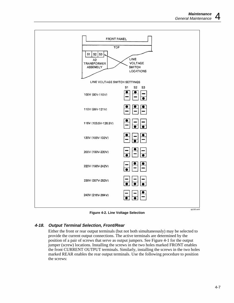
MaintenanceGeneral Maintenance 4
4-7
ajs16f.wmf
Figure 4-2. Line Voltage Selection
4-18. Output Terminal Selection, Front/RearEither the front or rear output terminals (but not both simultaneously) may be selected toprovide the current output connections. The active terminals are determined by theposition of a pair of screws that serve as output jumpers. See Figure 4-1 for the outputjumper (screw) locations. Installing the screws in the two holes marked FRONT enablesthe front CURRENT OUTPUT terminals. Similarly, installing the screws in the two holesmarked REAR enables the rear output terminals. Use the following procedure to positionthe screws:

5 220AInstruction Manual
4-8
CautionTo ensure proper instrument operation make sure that bothscrews are installed and that they are both in either the FRONTor REAR locations.
1. Disconnect the 5220A from line power.
2. Remove both the top and large inner covers from the 5220A.
3. Locate the output jumper screws as shown in Figure 4-1.
4. Install and secure the screws in the two FRONT or REAR holes, as desired.
5. Reinstall the top and inner covers.
4-19. Service ToolsThe 5220A comes equipped with an extender board for servicing other 5220A PCBassemblies. A storage slot for the board is provided in the 5220A PCB assemblies. SeeFigure 4-1 for the storage location.
4-20. Performance TestThe following paragraphs comprise a performance verification test that compares theinstrument’s performance to the specifications given in Section 1 of this manual. The testis recommended as an acceptance test when the unit is first received, and later as acalibration procedure to verify instrument accuracy at the scheduled calibration periods.It is also useful as an aid in troubleshooting.
Test equipment required for the performance test is listed earlier in Table 4-1. If therecommended equipment is not available, comparable instruments with equivalentspecifications may be substituted. To ensure optimum results, the test must be performedat an ambient temperature of 22 to 24 degrees Celsius, with a relative humidity of lessthan 85 %. Also the instrument should be allowed to warm up for at least 30 minutesbefore starting the performance test.
If the instrument does not meet the performance test, troubleshooting, repair, and/orcalibration adjustment is indicated. Procedures for calibration adjustment andtroubleshooting are given later in this section of the manual.
4-21. Initial ConditionsBefore starting the following procedures, condition the 5220A as follows:
1. Disconnect all input, output, and remote connections at the 5220A.
2. Install the top, bottom and inner covers if they have been removed.
3. Connect the unit to line power through an autotransformer set for the proper linevoltage, and set the POWER switch to ON. Only the STANDBY and FRONT LEDsshould light.
4. Allow the 5220A to warm up for at least 30 minutes before proceeding.

MaintenancePerformance Test 4
4-9
4-22. Front Panel TestsUse the following procedure to check the operation of the 5220A front-panel controls andLEDs:
1. With the unit in the standby mode, connect jumper wires between the enabled(front/rear) output terminals. Use a 4-inch length of 16-gauge insulated wire.
2. Press the OPR/STDBY pushbutton. The OPR LED should light and the STDBY LEDshould go out.
3. Press the INPUT pushbutton to select the rear input.
4. Return input control to the front panel by pressing the INPUT pushbutton. TheFRONT LED should light and the REAR LED should go out.
5. Remove the jumper wire from the output terminals. The unit should switch to thestandby mode and the OVERCOMPLIANCE LED should light.
6. Reinstall the jumper wire at the output terminals.
7. Clear the overcompliance condition by pressing the OPR/STDBY switch. Set the unitto the operate mode.
CautionThe THERMAL CUTOFF LED will light only when the outputstage of the 5220A is overheated. This is a failure mode thatshould not be invoked for test purposes. The LOCALpushbutton and the REMOTE, LOCAL LOCK OUT LEDs areremote control features that require remote commands foroperation.
4-23. Zero OutputThe following procedure checks the zero output of the 5220A in both the standby andoperate modes:
1. Connect the load resistor (0.1 ohm) to the enabled (front/rear) output terminals.
2. Connect the DVM to the sense terminals on the load resistor and select the 100 mVdc range.
3. With the 5220A in the standby mode, read the voltage drop across the load resistor.The reading should be 0 +/-5 µV dc.
4. Connect a short jumper wire between the front VOLTAGE INPUT terminals.
5. Set the 5220A to the operate mode. The OPERATE LED should be on and theSTANDBY LED off.
6. Read the output voltage on the DVM. It should be 0 +/-100 µV dc.
7. Set the 5220A to standby and remove the jumper wire from the VOLTAGE INPUTterminals.
8. Disconnect the load resistor from the output terminals on the 5220A.

5 220AInstruction Manual
4-10
4-24. DC Accuracy and Line RegulationThe following procedure is used to check the dc accuracy of the 5220A output current:
1. Connect the precision shunt to the enabled output terminals on the 5220A.
2. Connect the DVM to the sense terminals on the precision shunt. Observe polarity.
3. Set the DVM to the 200 mV dc range.
4. Connect the output of the dc voltage calibrator to the VOLTAGE INPUT terminalson the 5220A; positive to red, negative to black.
5. Set the dc voltage calibrator to the output shown in step 1 of Table 4-2 (+10.0000 Vdc).
6. Set the 5220A to the operate mode.
7. Using the DVM reading and the calibrated shunt valve, calculate the output current(I = E/R). The calculated value should be within the limits shown in the table.
8. Vary the line voltage +10 % from nominal and verify a less than 0.001 % change inoutput current.
9. Sequentially set the calibrator output to the voltages shown in steps 2 and 3 of Table4-2. At each voltage setting verify the 5220A output accuracy by repeating step 7 ofthis procedure.
10. Set the 5220A to the standby mode.
11. Set the dc voltage calibrator output to zero volts and disconnect it from the 5220A.
12. Disconnect the precision shunt from the 5220A output terminals.
Table 4-2. DC Accuracy Test
Step DC Calibrator Output (V dc) Calculated Output Current (Amps)
1 +10.0000 +9.9965 to +10.0035
2 +20.0000 +19.9940 to +20.0060
3 -10.0000 -10.0035 to –0.0065
4-25. Harmonic DistortionThis procedure is used to measure the harmonic distortion present at the output of the5220A.
1. Set the output of the ac voltage calibrator to zero and connect it to the 5220AVOLTAGE INPUT terminals.
2. Connect the load resistor (0.1 ohms) to the enabled (front/rear) output terminals.
3. Connect the distortion analyzer to load resistor sense terminals.
4. Set the ac voltage calibrator output to 20 V rms at 1 kHz.
5. Set the 5220A to the operate mode.
6. Measure the output distortion on the distortion analyzer. It should be less than orequal to 0.075 %.
NoteDo not use input filters when making this measurement.

MaintenancePerformance Test 4
4-11
7. Set the 5220A to the standby mode.
8. Disconnect the load resistor and the distortion analyzer from the 5220A outputterminals.
4-26. Frequency Response
NoteWhen high ac currents at high frequencies are being used, andminimization of inductive coupling is required, it is recommended that youtwist the current carrying leads between the 5220A and load. Also, anymeasuring instruments used with the load should be kept at least eighteeninches away the load to prevent radiation from affecting its reading.
The frequency response of the 5220A is checked using the following procedure:
1. Connect the precision shunt (.01 ohm) to the enabled (front/rear) output terminals.
2. Connect the true rms voltmeter to the sense terminals on the precision shunt.
3. Set the ac voltage calibrator output to the voltage and frequency shown in step 1 ofTable 4-3 (20.0000 V @ 100 Hz).
4. Set the 5220A to the operate mode.
5. Read the true rms voltmeter and calculate the current. It should indicate a currentwithin the limits shown for step 1.
6. Sequentially set the calibrator output to each of the frequencies shown in steps 2through 5 of Table 4-3. At each frequency verify that the measured current is withinthe limits given for that step.
7. Set the 5220A to the standby mode.
8. Disconnect the precision shunt from the 5220A output terminals.
Table 4-3. Frequency Response Test
Step AC Voltage Calibrator Output (V rms) Measured Output Current (Amps)
1 20 V @ 100 Hz 19.970 to 20.030*
2 20 V @ 300 Hz Reading 1 ±0.05 %
3 20 V @ 1 kHz Reading 1 ±0.05 %
4 20 V @ 3 kHz Reading 1 ±0.15 %
5 20 V @ 5 kHz Reading 1 ±0.25 %
* Includes limit of errors:1. 5220A 2. 5200A 3. Y5020 4. 931A
4-27. Overcurrent Trip TestThe following procedure will verify the accuracy of the overcurrent trip setting on the5220A:
1. Connect the load resistor (0.1 ohm) to the enabled (front/rear) output terminals.
2. Set the output of the ac voltage calibrator to 20.0000 V rms.
3. Set the 5220A to the operate mode.

5 220AInstruction Manual
4-12
4. Increase the ac voltage calibrator output in 1.0V rms increments. The 5220A shouldswitch to the standby mode at between 20.0 and 24.0 V rms. The OVERCURRENTLED should also light.
5. Set the ac voltage calibrator output to zero volts.
6. Disconnect the load resistor from the 5220A output terminals.
4-28. Overvoltage Trip TestThe following procedure is used to check the overvoltage trip setting on the 5220A:
1. Connect a 1 ohm ±5 %, 10 W resistor (Dale RH-10) to the enabled (front/rear) outputterminals on the 5220A.
2. Set the output of the 5220A to 3.0000 V rms.
3. Set the 5220A to the operate mode.
4. Increase the ac voltage calibrator output in 0.1 V rms increments. The 5220A shouldswitch to the standby mode with an input of 3.1 to 3.5 V rms. The OVERVOLTAGELED should also light.
5. Set the ac voltage calibrator output to zero volts and disconnect the unit from the5220A.
6. Remove the 1 ohm, 10 W resistor from the 5220A output terminals.
7. Set the 5220A POWER switch to OFF.
4-29. Calibration AdjustmentsThe calibration adjustment procedures given in the following paragraphs should beperformed after repair of the 5220A and/or when the unit fails the performance-testrequirements. If the unit will not respond to, or meet the limits of the adjustmentprocedures, troubleshooting and repair is indicated. Equipment required for thecalibration adjustments is listed earlier in Table 4-1.
All calibration adjustments are accessible when the top and large inner covers areremoved from the 5220A. Figure 4-1 identifies the location of the assemblies, test points,and adjustments that must be accessed to complete the calibration adjustment procedures.
To ensure optimum results, the calibration adjustments must be performed at an ambienttemperature of 22 to 24 degrees Celsius, with a relative humidity of less than 85 %. Alsothe unit should be allowed to warmup in the operate mode (with the top cover in place)for at least 30 minutes before starting the adjustment procedures.

MaintenanceCalibration Adjustments 4
4-13
4-30. Initial ConditionsBefore starting the following procedures, condition the 5220A as follows:
1. Disconnect all input and remote connections to the 5220A, and connect a shortjumper wire between the selected output terminals.
2. Connect the unit to line power and set the POWER switch to ON. Only the STDBYand FRONT LEDs should light.
3. Set the 5220A to the operate mode and allow it to warmup for at least 30 minutes.
4. Remove the top and large inner cover from the unit, and complete the followingprocedures.
4-31. Input Offset AdjustmentThe following procedure is used to adjust input offset (R6) on the A5 Preamplifier PCBAssembly:
1. Connect the load resistor (0.1 ohm) to the enabled (front/rear) 5220A outputterminals.
2. Connect the DVM to the sense terminals on the load resistor and select the 100 mVdc range.
3. Connect a short jumper wire between the front VOLTAGE INPUT terminals.
4. Set the 5220A to the operate mode.
5. Adjust R6 on the A5 Preamplifier PCB Assembly for a DVM reading of -.010 to -.010 mV dc (0 +10 µV dc).
6. Set the 5220A to the standby mode.
4-32. Driver Offset AdjustmentThe following procedure is used to adjust input offset (R6) on the A6 Driver PCBAssembly. The procedure is accomplished with the 5220A in the standby mode:
1. Jumper test lead between TP7 (-15 V dc) on the A4 Regulator and TP4 (Turn on 1)on the A8 Analog Control. This enables the A8 Analog Control and A7 Output whilethe A5 Preamplifier is clamped to zero (standby).
2. Adjust R6 on the A6 Driver for a DVM reading of -1.000 to +1.000 mV dc.
3. Disconnect the test lead from TP4 and TP7.
4. Remove the load resistor from the 5220A output terminals.
5. Remove the jumper wire from the front-panel VOLTAGE INPUT terminals.

5 220AInstruction Manual
4-14
4-33. Output Bias AdjustmentThis procedure is used to adjust the bias current for both the A6 Driver and the A7Output. The bias adjustment (R13) is located on the A6 Driver PCB Assembly.
1. Connect the ac voltage calibrator to the front-panel VOLTAGE INPUT terminals onthe 5220A.
2. Connect the load resistor (.1 ohm) to the enabled output terminals on the 5220A.
3. Connect the distortion analyzer input to the sense terminals on the load resistor.
4. Set the ac voltage calibrator for a 20 V rms, 1 kHz output.
5. Set the 5220A to the operate mode.
6. Measure the distortion and adjust R13 for a minimum indication. At the final setting,distortion should measure less than 0.04 %.
7. Set the 5220A to the standby mode.
8. Disconnect the distortion analyzer and the load resistor from the 5220A.
4-34. DC Accuracy AdjustmentThis procedure is used to adjust R3 on the A5 Preamplifier PCB Assembly. Thisadjustment controls the accuracy of the dc output current.
1. Connect the precision shunt (.01 ohm) to the enabled output terminals on the 5220A.
2. Connect the DVM to the sense terminals on the precision shunt. Observe polarity.
3. Connect the output of the dc voltage calibrator to the VOLTAGE INPUT terminalson the 5220A; positive to red, negative to black.
4. Set the dc voltage calibrator for an output of +10.0000 V dc.
5. Set the 5220A to the operate mode.
6. Adjust R3 on the A5 Preamplifier for a voltage reading in millivolts that is 10 timesthe calibrated value of the precision shunt in milliohms. The adjustment should bewithin +0.002 mV dc of the calculated value. For example: if the calibrated value ofthe shunt is 0.0100253, adjust R3 for a DVM reading of .100253 V dc or 100.253+0.002 mV dc.
7. Set the 5220A to the standby mode.
8. Disconnect both the dc voltage calibrator and the precision shunt from the 5220A.
4-35. Frequency ResponseThe following procedure is used to adjust the frequency response of the 5220A. Theadjustment is made at C4 on the A5 Preamplifier PCB Assembly.
1. Connect the precision shunt to the enabled output terminals on the 5220A.
2. Connect the true rms voltmeter to the sense terminals on the precision shunt.
3. Set the output of the ac voltage calibrator to 10 V rms, 1 kHz.
4. Set the 5220A to the operate mode.
5. Note the reading on the rms voltmeter.
6. Change the frequency of the calibrator output to 5 kHz.
7. Adjust trimmer capacitor C4 on the A5 Preamplifier PCB to obtain the same readingon the rms voltmeter as that noted in step 5.

MaintenanceReplacement of Selected Components 4
4-15
8. Set the 5220A to the standby mode.
9. Disconnect the shunt and voltmeter from the 5220A output terminals.
4-36. Overcurrent AdjustmentThis procedure is used to adjust the overcurrent trip level of the 5220A. The overcurrentadjustment (R21) is located on the A8 Analog Control PCB Assembly.
1. Connect the load resistor (0.1 ohm) to the enabled output terminals on the 5220A.
2. Set the calibrator output to 23.5 V rms, 50 Hz.
3. Set the 5220A to the operate mode. If the unit switches back to standby, turn R21 (onthe A8 Analog Control PCB Assembly) counterclockwise until the operate mode canbe enabled.
4. Adjust R21 clockwise until the 5220A switches to the standby mode. Both theSTDBY and OVERCURRENT LEDs should light.
5. Disconnect the 0.1 ohm load resistor from the 5220A output terminals.
4-37. Overvoltage AdjustmentThis procedure is used to adjust the overvoltage trip level for the 5220A. The overvoltageadjustment (R9) is located on the A8 Analog Control PCB Assembly.
1. Connect the 1 ohm load resistor to the enabled output terminals on the 5220A.
2. Set the ac voltage calibrator output for 3.3 V rms, 50 Hz.
3. Set the 5220A to the operate mode. If the unit switches back to standby, turn R9 (onthe A8 Analog Control PCB Assembly) counterclockwise until the operate mode canbe enabled.
4. Adjust R9 clockwise until the 5220A switches to the standby mode. Both the STDBYand OVERCOMPLIANCE LEDs should light.
5. Disconnect the load resistor and the ac voltage calibrator from the 5220A.
6. Set the 5220A POWER switch to OFF.
7. Disconnect the unit from line power.
8. Install the inner cover and top cover on the 5220A.
4-38. Replacement of Selected ComponentsThe A5 Preamplifier PCB Assembly contains a series of three selected parts that mayhave to be changed after repairs have been made on the PCB. All three selected parts areresistors. Two (R11, R12) are associated with the Input Offset Adjustment (R6); the third(R13) affects the DC Accuracy Adjustment (R3). Resistors R11 and R12 are selected toplace R6 at approximately midrange when it is properly adjusted. Resistor R13 is selectedto accomplish the same thing for R3. When the travel of either R3 or R6 limits properadjustment, the associated selected resistor(s) should be replaced. Follow the appropriateprocedure for parts selection.

5 220AInstruction Manual
4-16
4-39. Resistors R11 and R12Resistors R11 and R12 are associated with the Input Offset Adjustment procedure and thesetting of the ZERO ADJ potentiometer R6. Use the following procedure to select theproper replacements for R11 and R12:
1. Disconnect the 5220A from line power.
2. Remove the top and large inner covers from the unit.
3. Remove the two fuses (F1 and F2) from the A3 Cap Bus PCB Assembly.
4. Mount the A5 Preamplifier PCB Assembly on the extender board and install jumperwires on the PCB at the following points:
a. TP1 to TP5
b. TP3 to TP4
c. Short across R11
d. Short across R12
5. Disconnect the red and black Current Shunt sense lead from the motherboard(connections are located near the A5 Preamplifier connector). On A8 the AnalogControl, short TP9 to TP13 to prevent a false overcurrent trip.
6. Set the digital voltmeter to the 100 mV dc range and connect its input to TP4(+) andTP5(-) on the A5 Preamplifier PCB Assembly.
7. Adjust R6 on the A5 Preamplifier to the full ccw (counterclockwise) position.
8. Connect the 5220A to line power and set the POWER switch to ON.
9. Select the operate mode using the STDBY/OPR switch.
10. Note the DVM reading. It should read within the range of +/-1.300 mV dc.
11. Adjust R6 on the A5 Preamplifier PCB to the full cw (clockwise) position and notethe reading. The DVM reading should increase in a positive direction.
12. Calculate the difference between the DVM readings taken in steps 10 and 11. Thedifference should be 350 µV +/- 70 µV dc.
13. Determine the average reading of steps 10 and 11 and adjust R6 for that reading onthe DVM. Then perform step a, b, or c as required:
a. If the DVM reading is within the range of +/-0.087 mV dc, replace both R11 andR12 with shorting wires (0 Ω).
b. If the DVM reading is negative, refer to Table 4-4, and replace R12 with theappropriate resistor. Replace R11 with a shorting wire.
c. If the DVM reading is positive, refer to Table 4-4 and replace R11 with theappropriate resistor. Replace R12 with a shorting wire.
14. Set the POWER switch to OFF and disconnect the 5220A from line power.
15. Install the two fuses (F1 and F2) on the A3 Cap Bus PCB Assembly.
16. Remove the jumpers from TP1-TP5 and TP3-TP4.
17. Disconnect the DVM from TP4 and TP5.
18. Remove the A5 Preamplifier PCB from the extender board.
19. Reconnect the red and black current shunt sense leads to the motherboard.
20. Install the A5 Preamplifier PCB Assembly in its slot.
21. Perform the Calibration Adjustment procedures.
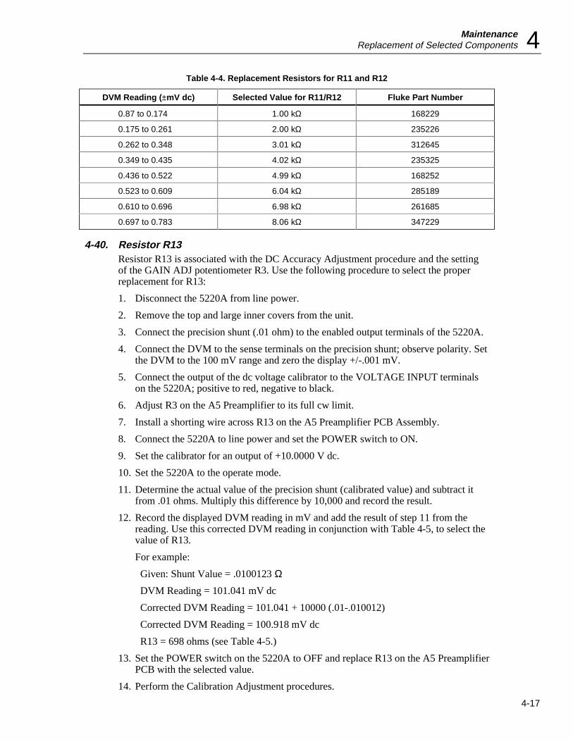
MaintenanceReplacement of Selected Components 4
4-17
Table 4-4. Replacement Resistors for R11 and R12
DVM Reading (±mV dc) Selected Value for R11/R12 Fluke Part Number
0.87 to 0.174 1.00 kΩ 168229
0.175 to 0.261 2.00 kΩ 235226
0.262 to 0.348 3.01 kΩ 312645
0.349 to 0.435 4.02 kΩ 235325
0.436 to 0.522 4.99 kΩ 168252
0.523 to 0.609 6.04 kΩ 285189
0.610 to 0.696 6.98 kΩ 261685
0.697 to 0.783 8.06 kΩ 347229
4-40. Resistor R13Resistor R13 is associated with the DC Accuracy Adjustment procedure and the settingof the GAIN ADJ potentiometer R3. Use the following procedure to select the properreplacement for R13:
1. Disconnect the 5220A from line power.
2. Remove the top and large inner covers from the unit.
3. Connect the precision shunt (.01 ohm) to the enabled output terminals of the 5220A.
4. Connect the DVM to the sense terminals on the precision shunt; observe polarity. Setthe DVM to the 100 mV range and zero the display +/-.001 mV.
5. Connect the output of the dc voltage calibrator to the VOLTAGE INPUT terminalson the 5220A; positive to red, negative to black.
6. Adjust R3 on the A5 Preamplifier to its full cw limit.
7. Install a shorting wire across R13 on the A5 Preamplifier PCB Assembly.
8. Connect the 5220A to line power and set the POWER switch to ON.
9. Set the calibrator for an output of +10.0000 V dc.
10. Set the 5220A to the operate mode.
11. Determine the actual value of the precision shunt (calibrated value) and subtract itfrom .01 ohms. Multiply this difference by 10,000 and record the result.
12. Record the displayed DVM reading in mV and add the result of step 11 from thereading. Use this corrected DVM reading in conjunction with Table 4-5, to select thevalue of R13.
For example:
Given: Shunt Value = .0100123 Ω
DVM Reading = 101.041 mV dc
Corrected DVM Reading = 101.041 + 10000 (.01-.010012)
Corrected DVM Reading = 100.918 mV dc
R13 = 698 ohms (see Table 4-5.)
13. Set the POWER switch on the 5220A to OFF and replace R13 on the A5 PreamplifierPCB with the selected value.
14. Perform the Calibration Adjustment procedures.

5 220AInstruction Manual
4-18
Table 4-5. Replacement Resistors for R13
Corrected DVM Indication (mV dc) Selected Value for R13 (Ω) Fluke Part Number
102.000 to 101.800 1740 Ω 357756
101.800 to 101.600 1500 Ω 376947
101.600 to 101.400 1282 Ω 330472
101.400 to 101.200 1100 Ω 347161
101.200 to 101.000 900 Ω 460519
101.000 to 100.800 698 Ω 289330
100.800 to 100.600 499 Ω 289256
100.600 to 100.400 301 Ω 289173
100.400 to 100.200 100 Ω 357400
100.200 to 100.000 0 Ω NA
4-41. TroubleshootinghCaution
Static discharge can damage MOS components contained inthe 5220A. To prevent this possibility use the followingprecautions when troubleshooting and/or repairing the unit.
• Never remove, install, or otherwise connect, or disconnect PCBs and/or componentswithout disconnecting, the unit from line power.
• Perform all repairs at a static-free work station.
• Do not handle ICs or PCBs by their connectors.
• Use static ground straps to discharge repair personnel.
• Use conductive foam to store replacement or removed ICs.
• Remove all plastic, vinyl, and Styrofoam products from the work area.
• Use a grounded soldering iron.
A troubleshooting guide for the 5220A is given in Table 4-4 and 4-5. The guide is in theform of a tabular flow chart and is recommended for use in isolating a mainframemalfunction to the PCB (board) level. Details necessary to troubleshoot faulty PCBs tothe component level can be derived from the schematic diagrams given in Section 8, andthe theory of operation in Section 3.
When using the troubleshooting guides, the following notes apply:
• Do not start in the middle of the procedure. Any given step assumes that the previoussteps have been completed. Complete Table 4-4 before going on to Table 4-5.
• All measurements using external test equipment are made at test points on the variousPCB assemblies. See Figure 4-3 for test point location/identification.

MaintenanceTroubleshooting 4
4-19
ajs17f.wmf
Figure 4-3. Test Point Location/Identification

5 220AInstruction Manual
4-20
ajs18f.wmf
Figure 4-4. Flowchart Summary of Mainframe and Digital SectionTroubleshooting Guide
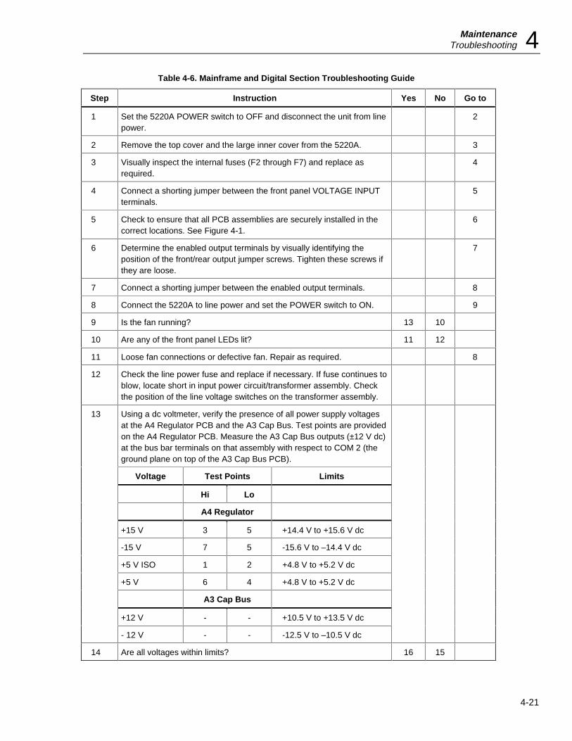
MaintenanceTroubleshooting 4
4-21
Table 4-6. Mainframe and Digital Section Troubleshooting Guide
Step Instruction Yes No Go to
1 Set the 5220A POWER switch to OFF and disconnect the unit from linepower.
2
2 Remove the top cover and the large inner cover from the 5220A. 3
3 Visually inspect the internal fuses (F2 through F7) and replace asrequired.
4
4 Connect a shorting jumper between the front panel VOLTAGE INPUTterminals.
5
5 Check to ensure that all PCB assemblies are securely installed in thecorrect locations. See Figure 4-1.
6
6 Determine the enabled output terminals by visually identifying theposition of the front/rear output jumper screws. Tighten these screws ifthey are loose.
7
7 Connect a shorting jumper between the enabled output terminals. 8
8 Connect the 5220A to line power and set the POWER switch to ON. 9
9 Is the fan running? 13 10
10 Are any of the front panel LEDs lit? 11 12
11 Loose fan connections or defective fan. Repair as required. 8
12 Check the line power fuse and replace if necessary. If fuse continues toblow, locate short in input power circuit/transformer assembly. Checkthe position of the line voltage switches on the transformer assembly.
Using a dc voltmeter, verify the presence of all power supply voltagesat the A4 Regulator PCB and the A3 Cap Bus. Test points are providedon the A4 Regulator PCB. Measure the A3 Cap Bus outputs (±12 V dc)at the bus bar terminals on that assembly with respect to COM 2 (theground plane on top of the A3 Cap Bus PCB).
Voltage Test Points Limits
Hi Lo
A4 Regulator
+15 V 3 5 +14.4 V to +15.6 V dc
-15 V 7 5 -15.6 V to –14.4 V dc
+5 V ISO 1 2 +4.8 V to +5.2 V dc
+5 V 6 4 +4.8 V to +5.2 V dc
A3 Cap Bus
+12 V - - +10.5 V to +13.5 V dc
13
- 12 V - - -12.5 V to –10.5 V dc
14 Are all voltages within limits? 16 15

5 220AInstruction Manual
4-22
Table 4-6. Mainframe and Digital Section Troubleshooting Guide (cont.)
Step Instruction Yes No Go to
15 Check the line voltage switch settings on A2 TransformerAssembly. They should be set to comply with the local linevoltage. If some voltages are in limits and some are out, theproblem is on the A4 Regulator or the A3 Cap Bus. If a voltage islow, check for power supply loading. If a voltage is high, theregulator IC is likely the cause.
Front Panel Tests
16 Complete the Front Panel Tests described earlier underPerformance Test.
17
17 Does the 5220A respond as described in the Front Panel Tests?
18 Do one or more LEDs light? 20 19
19 Operating voltage (+5 V dc) is not present at either the A9 FrontPanel PCB or the A10 Logic PCB. Repair as required.
20 Can the standby/operate modes be selected?
NoteThe jumper wire must be installed between theenabled output terminals.
21 Is the OVERCURRENT or OVERCOMPLIANCE LED lit? 23 22
22 Defective switch, LED, or standby/operate circuit (on the A10Logic PCB).
16
23 Set the POWER switch to OFF, then ON.
24 Is the OVERCURRENT or OVERCOMPLIANCE LED lit? 34 25
25 Connect a 0.1 Ω resistor between the selected output terminals,then connect a DVM across the 0.1 Ω resistor.
26
26 Connect a jumper wire between TP4 (Turn on 1) on the A8Analog Control PCB and TP7 (-15 V) on the A4 Regulator PCB.
27
27 With the 5220A in standby, adjust R6 on the A6 Driver for a DVMreading of 0 V ±1.0 mV.
28
28 Can a 0 V DVM reading be obtained? 30 29
29 The A6 Driver and/or A7 Output Assemblies are defective.Repair as required.
16
30 The A6 Driver and A7 Output Assemblies are functional.Remove the jumper from between TP4 and the A8 AnalogControl PCB and TP17 on the A4 Regulator.
31
31 Press the STBY/OPR switch. 32
32 Can the operate mode be selected? 33 34

MaintenanceTroubleshooting 4
4-23
Table 4-6. Mainframe and Digital Section Troubleshooting Guide (cont.)
Step Instruction Yes No Go to
33 The mainframe and digital section are operational; thetransconductance amplifier (A5, A6, A7) is defective. Check outand repair the transconductance amplifier using Table 4-7,Analog Section Troubleshooting Guide.
16
34 Is OVERCURRENT LED lit? 35 36
35 Check the following and repair as required:
1. Open feedback loop, current shunt to A5 Preamplifier.
2. Overcurrent detector on A8 PCB.
3. Failure status logic on A10 PCB.
4. Defective A5 Preamplifier PCB.
36 Is OVERCOMPLIANCE LED lit? 37 38
37 Check the following and repair as required:
1. Overvoltage detector on A8 PCB.
2. Open loop on transconductance amplifier (A5, A6, A7PCBs).
3. Failure status circuit on the A10 PCB.
4. Open load or open circuit between output amplifier andoutput terminals.
16
38 Check timing logic on the A10 Logic PCB, and the level shifterson the A8 Analog Control PCB. Repair as required.
16

5 220AInstruction Manual
4-24
ajs19f.wmf
Figure 4-5. Flowchart Summary of Analog Section Troubleshooting Guide

MaintenanceTroubleshooting 4
4-25
Table 4-7. Analog Section Troubleshooting Guide
Step Instruction Yes No Go to
1 Complete the troubleshooting procedure given in Table 4-6. 2
2 Set the 5220A POWER switch to OFF. 3
3 Connect a jumper wire between the front panel VOLTAGEINPUT terminals.
4
4 Connect a 0.1 Ω resistor between the selected output terminals,then connect a DVM across the 0.1 Ω resistor.
5
5 Set the POWER switch to ON and select the operate mode. 6
6 Does the 5220A remain in the operate mode? 8 9
7 If the 5220A trips to standby and indicates an overcompliance orovercurrent condition, the A5 Preamplifier PCB is at fault. Checkvoltage levels on the active components on the A5 preamplifierPCB while the unit is in standby. Repair as required.
8
8 Using a tuning tool, adjust R1, Zero Adjust, on the A5Preamplifier PCB for a DVM reading of 0 V ±3 µV dc. Theadjustment should cover a range or 0 V ±5 µV.
9
9 Can R6 be adjusted for a DVM reading or 0 V ±3 µV? 17 10
10 Connect the DVM from TP4 (high) to TP5 (low) on the A5Preamplifier PCB Assembly. With the 5220A in the operatemode the DVM should read –15 V dc.
11
11 Does the DVM read –15 V dc? 13 14
12 Troubleshoot the Turn on 1 circuit starting with the level-shiftingtransistors Q3 and Q4 on the A8 Analog Control PCB Assembly.Then check for a T1 output from U22 on the A10 Logic PCBAssembly. Repair as required.
13 Connect the DVM from TP6 (high) to TP5 (low) on the A5Preamplifier PCB Assembly. With the 5220A in the operatemode, the DVM should read –15 V dc.
14
14 Does the DVM read –15 V dc? 16 15
15 Troubleshoot the FET Drive 1 circuit starting with the level-shifting transistors Q1 and Q2 on the A8 Analog Control PCBAssembly. Then check for a T2 output from U22 on the A10Logic PCB Assembly. Repair as required.
8
16 The A5 Preamplifier PCB Assembly is defective. Check voltagelevels on the active components on the A5 Preamplifier while theunit is in standby. Repair as required.
8
17 The A5 Preamplifier, A6 Driver, and A7 Output stages areoperating properly. Set the 5220A to standby, remove andreplace the front panel short at the VOLTAGE INPUT terminalswith a 1.0 V dc voltage source; positive to red, negative to black.
18
18 Reconnect the DVM across the 0.1 Ω resistor to the outputterminals.
19

5 220AInstruction Manual
4-26
Table 4-7. Analog Section Troubleshooting Guide (cont.)
Step Instruction Yes No Go to
19 Set the 5220A to the operate mode and read the DVM. 20
20 Does the DVM read approximately +0.1 V dc? 26 22
21 Does the DVM read approximately 0 V? 22 23
22 Check relay K1 and associated drive circuits on the A5Preamplifier PCB Assembly. Also check resistors R1, R2, andR13 for open circuits. If these are OK, check the Relay 1 drivesignal from the A10 Logic PCB Assembly.
23 Is the DVM reading greater than 0.010 V dc? 24 25
24 The A6 Driver or A7 Output stage is defective. Check voltagelevels on active components to isolate the fault. Repair asrequired.
20
25 The A5 preamplifier is defective. Check voltage levels on activecomponents to isolate the fault. Repair as required.
20
26 The 5220A is operational. Verify instrument compliance withpublished specifications by completing the Performance Testgiven earlier in this section of the manual.
-
5-1
Section 5List of Replaceable Parts
5-1. IntroductionThis section contains an illustrated list of replaceable parts for 5220A. Parts are listed byassembly; alphabetized by reference designator. Each assembly is accompanied by anillustration showing the location of each part and its reference designator. The parts listsgive the following information:
• Reference designator
• An indication if the part is subject to damage by static discharge
• Description
• Fluke stock number
• Total quantity
• Any special notes (i.e., factory-selected part)
CautionA h symbol indicates a device that may be damaged by staticdischarge.
5-2. How to Obtain PartsElectrical components may be ordered directly from the manufacturer by using themanufacturers part number, or from the Fluke Corporation and its authorizedrepresentatives by using the part number under the heading FLUKE STOCK NO. In theU.S., order directly from the Fluke Parts Dept. by calling 1-800-526-4731. Parts priceinformation is available from the Fluke Corporation or its representatives. Prices are alsoavailable in a Fluke Replacement Parts Catalog which is available on request.
In the event that the part ordered has been replaced by a new or improved part, thereplacement will be accompanied by an explanatory note and installation instructions, ifnecessary.
To ensure prompt delivery of the correct part, include the following information whenyou place an order:
• Part number and revision level of the PCA containing the part.
• Reference designator

5 220AInstruction Manual
5-2
• Fluke stock number
• Description (as given under the Description heading)
• Quantity
• Instrument Model, Serial Number, and Firmware Numbers
5-3. Manual Status InformationThe Manual Status Information table that precedes the parts list defines the assemblyrevision levels that are documented in the manual. Revision levels are printed on thecomponent side of each PCA.
5-4. Newer InstrumentsChanges and improvements made to the instrument are identified by incrementing therevision letter marked on the affected PCA. These changes are documented on a manualsupplement which, when applicable, is included with the manual.
5-5. Service CentersTo locate an authorized service center, call Fluke using any of the phone numbers listedbelow, or visit us on the World Wide Web: www.fluke.com
• 1-800-443-5853 in U.S.A and Canada
• 31 40 267 8200 in Europe
• 1-425-356-5500 from other countries
NoteThis instrument may contain a Nickel-Cadmium battery. Do not mix withthe solid waste stream. Spent batteries should be disposed of by a qualifiedrecycler or hazardous materials handler. Contact your authorized Flukeservice center for recycling information.
W WarningThis instrument contains two fusible resistors (PN 650085). Toensure safety, use exact replacement only.
Manual Status Information
Ref. or Option No. Assembly Name Fluke Part No. Revision Level
A1 Motherboard PCB Assembly 491209 D
A3 Capacitor Bus PCB Assembly 497446
A4 Regulator PCB Assembly 489690 E
A5 Preamplifier PCB Assembly 487702 T
A6 Driver PCB Assembly 540146 E
A7 Output PCB Assembly 540138 F
A8 Analog Control PCB Assembly 491241 G
A9 Front Panel PCB Assembly 491217 B
A10 Logic PCB Assembly 491258 G

List of Replaceable PartsService Centers 5
5-3
A11 MIS Bus Interface PCBAssembly
491266 C
A13 Output Termination PCBAssembly
491274 B

5 220AInstruction Manual
5-4
Table 5-1. 5220A Final Assembly
ReferenceDesignator Description
Fluke PartNo.
TotalQuantity
A1 h Motherboard PCB Assembly 491209 1
A2 Power Transformer Assembly 491282 1
A3 h Capacitor Bus PCB Assembly 476994 1
A4 h Regulator PCB Assembly 489690 1
A5 h Preamplifier PCB Assembly 947205 1
A6 h Driver PCB Assembly 540146 1
A7 h Output PCB Assembly 540138 1
A8 h Analog Control PCB Assembly 491241 1
A9 h Front Panel PCB Assembly 491217 1
A10 h Logic PCB Assembly 491258 1
A11 h MIS Bus Interface PCB Assembly 491266 1
A12 Shunt Assembly 491290 1
A13 h Output Termination PCB Assembly 491274 2
A14 h Extender PCB Assembly 486217 1
B1 Venturi Muffin Fan, 4.5 in 103374 1
C1-C8 Capacitor, AL, 50,000 µF, +100-10 %, 15 V, Hi Term. 423525 8
C9 Capacitor, CER, 0.05 µF, +80-20 %, 1,000 V, Z5U 355420 1
CR1, CR3 Diode, SI, 50 PIV, 20.0 A 483206 2
CR2, CR4 Diode, SI, 50 PIV, 20.0 A 483214 2
E1, E2 Terminal Ring, 0.087 & 0.195, Solder 101048 2
F1 W Fuse, 0.25 x 1.25, 3 A ,250 V, Slow 109280 1
F2, F3 W Fuse 0.25 x 1.25, 30 A, 32 V, Fast 500793 2
H1 Screw, Cap, Sckt, Steel, 8-32 x 0.375 295105 8
H2 Screw, Machine, FH, P, Steel, 8-32 x 0.312 281725 14
H3 Screw, Machine, FHU, P, SS, 6-32 x 0.250 320093 16
H4 Screw, Machine, PH, P, Steel, 6-32 x 0.250 152140 80
H5 Screw, Machine, FH, P, Steel, 8-32 x 0.375 114116 8
H6 Nut, Machine, Hex, Nylon, 8-32 110593 8
H7 Screw, Machine, PH, P, Steel, 6-32 x 0.375 152165 10
H8 Screw, Machine, RHSL, Nylon, 8-32 x 1/2 501569 4
H9 Washer, Lock, Internal, Steel, 0.267 ID 110817 4
H10 Nut, Machine, Hex, BR, 10-32 529032 2

List of Replaceable PartsService Centers 5
5-5
Table 5-1. 5220A Final Assembly (cont.)
ReferenceDesignator Description
Fluke PartNo.
TotalQuantity
H11 Washer, Lock, Internal, Steel, #4 110403 2
H12 Nut, Machine, Hex, Steel, 4-40 110635 2
H13 Screw, Machine, PH, P, Steel, 6-32 x 0.500 152173 13
H14 Nut, Machine, Hex, BR, 1/4-28 110619 9
H15 Washer, Shoulder, Fiber, 0.250 ID 110833 4
H16 Screw, Machine, PH, P, Steel, 8-32 x 0.500 159749 5
H17 Nut, Machine, Hex, Steel, 8-32 110544 10
H18 Screw, Machine, PH, P, Steel, 10-32 x 0.375 114314 16
H19 Washer, Flat, Steel, 0.265, 0.500, 0.031 110718 4
H20 Washer, Flat, Teflon, 0.366 x 0.266 x 0.050 543314 4
H21 Screw, Machine, PH, P, Steel, 6-32 x 0.625 152181 8
H22 Screw, Machine, PH, P, Steel, 6-32 x 1.500 114181 4
H23 Screw, Machine, PH, P, Steel, 8-32 x 0.375 114124 14
H24 Screw, Machine, PH, P, Steel, 10-32 x 0.625 114066 4
H25 Washer, Lock, External, Steel, 0.500 175943 1
MP1 Panel, Front 479618 1
MP2 Corner Handle, Front, 7 in 394320 2
MP3 Cover, Top 522524 1
MP4 Bracket, Front Panel 486068 2
MP5 Cover, Power Supply 489500 1
MP6 M07-800-415 Decal Covers, Plastic 394403 4
MP7 Plastic Part, Hole Plug, Polyethylene, 0.312 187799 7
MP8 Cover Plate, Digital Connector 502781 1
MP9 Side Trim-21 in 526004 2
MP10 Panel, Rear 485888 1
MP11 Shim, Rear Corner 486050 2
MP12 Corner, Rear 486076 2
MP13 Decal, Rear 502799 1
MP14 Plate, Rear Output 485995 1
MP15 Plate, Front Output 485987 1
MP16 Output Bus, Minus 489526 1
MP17 Output Bus, Plus- Forward 486534 1

5 220AInstruction Manual
5-6
Table 5-1. 5220A Final Assembly (cont.)
ReferenceDesignator Description
Fluke PartNo.
TotalQuantity
MP18 Output Bus, Plus- Aft 486542 1
MP19 Output Bus, Spacer 486559 1
MP20 Assembly, Red 10-32 Binding Post Bracket 794404 2
MP21 Assembly, Black 10-32 Binding Post Bracket 794412 2
MP22 Shunt Bus, Minus 490524 1
MP23 Shunt Bus, Plus 497974 1
MP241 Banana Jack, Panel 101550 4
MP25 Spacer, Round, Nylon, 6-32 x 1.063 104174 4
MP26 Bracket, Fan & Power Supply 485953 1
MP27 Cable Tie, 4.0 Length, 0.100 Width, 0.75 Diameter 172080 2
MP28 Binding Post Part, Head, Brass, 1/4-28 102889 1
MP29 Bushing, Snap-in, Nylon, 0.250 ID 102996 1
MP30 Terminal, Insulated, Standoff, Bifurcated 271650 2
MP31 Power Plug, Panel, 6 A, 250 V, 3-wire 284166 1
MP32 Card Guide, Nylon, 4.50 x 0.076 2-snap 256461 12
MP33 Binding Post, Brass, 1/4-28 102707 1
MP34 Holder Part, Fuse, Cap, 1/4 x 1-1/4 460238 1
MP35 Heatsink, Diode 502179 1
MP36 Insulating Part, Diode, Silicone, Washer 500785 4
MP37 Bus, Capacitor 497982 1
MP38 Chassis Side, Left 485896 1
MP39 Chassis Side, Right 485904 1
MP40 Chassis, Bottom 485912 1
MP41 Bulkhead, Front 485920 1
MP42 Bulkhead, Rear 485938 1
MP43 Partition, Rear 485946 1
MP44 Capacitor Tray 486035 1
MP45 Plate, Front Input 485979 1
MP46 Assembly, Red 6-32 Binding Post Bracket 794453 1
MP47 Assembly, Black 6-32 Binding Post Bracket 794461 1
MP48 Fan Accessory, Filter, AL with Foam 542118 1
MP49 Cover, Bottom 522532 1

List of Replaceable PartsService Centers 5
5-7
Table 5-1. 5220A Final Assembly (cont.)
ReferenceDesignator Description
Fluke PartNo.
TotalQuantity
MP50 Foot, Bail Stand 292870 4
MP51 Spacer, Capacitor 489484 2
MP52 Filter, Retainer 576967 1
MP54 Nameplate, 0.350 x 1.3, Serial Number 472795 1
MP55 Cover, Shunt 489948 1
R2, R5 Resistor, CC, 100, ±10 %, 2 W 109934 2
TM1 5220A Instruction Manual 491936 1
VR1, VR22 Zener, Transient Suppressor, 7.5 V, 10 % 904896 2
W1 Line Cord, 5-15/IEC, 3-18 AWG, SVT, 7.5 ft 284174 1
W2 Cable, Fan/Power 491308 1
W3 Fan-Cable 629188 1
XF1 Holder Part, Fuse, Body, 1/4 x 1-1/4, 5 x 20 mm 460329 1
XF2, XF3 Fuse, Clip, PCB, 1/4 x 1-1/4 756460 4
Not Shown Recommended Spare Parts Kit 756460 -
h Indicates a static-sensitive part.
1. This item consists of a plug, a washer, and a hex nut.
2. These parts are located on the A1 Motherboard pcb assembly schematic.

5 220AInstruction Manual
5-8
ajs20f.wmf
Figure 5-1. 5220A Final Assembly

List of Replaceable PartsService Centers 5
5-9
ajs21f.wmf
Figure 5-1. 5220A Final Assembly (cont.)
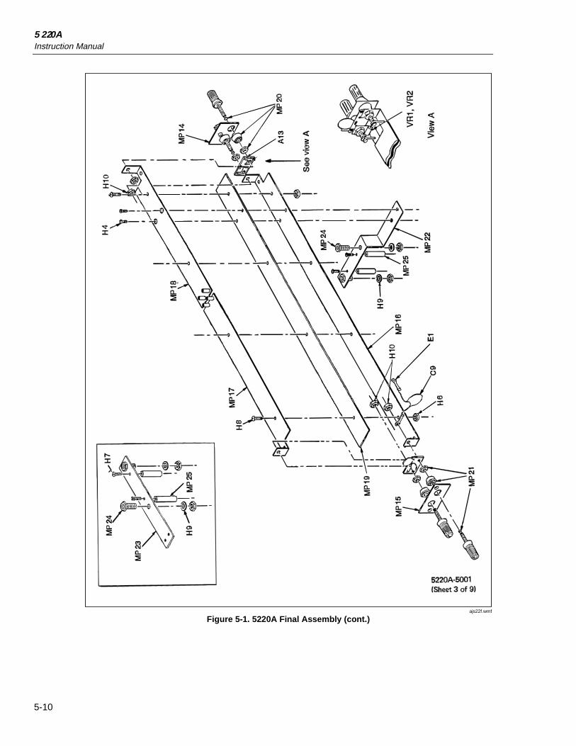
5 220AInstruction Manual
5-10
ajs22f.wmf
Figure 5-1. 5220A Final Assembly (cont.)
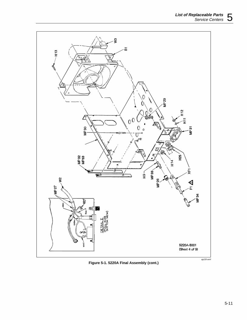
List of Replaceable PartsService Centers 5
5-11
ajs23f.wmf
Figure 5-1. 5220A Final Assembly (cont.)
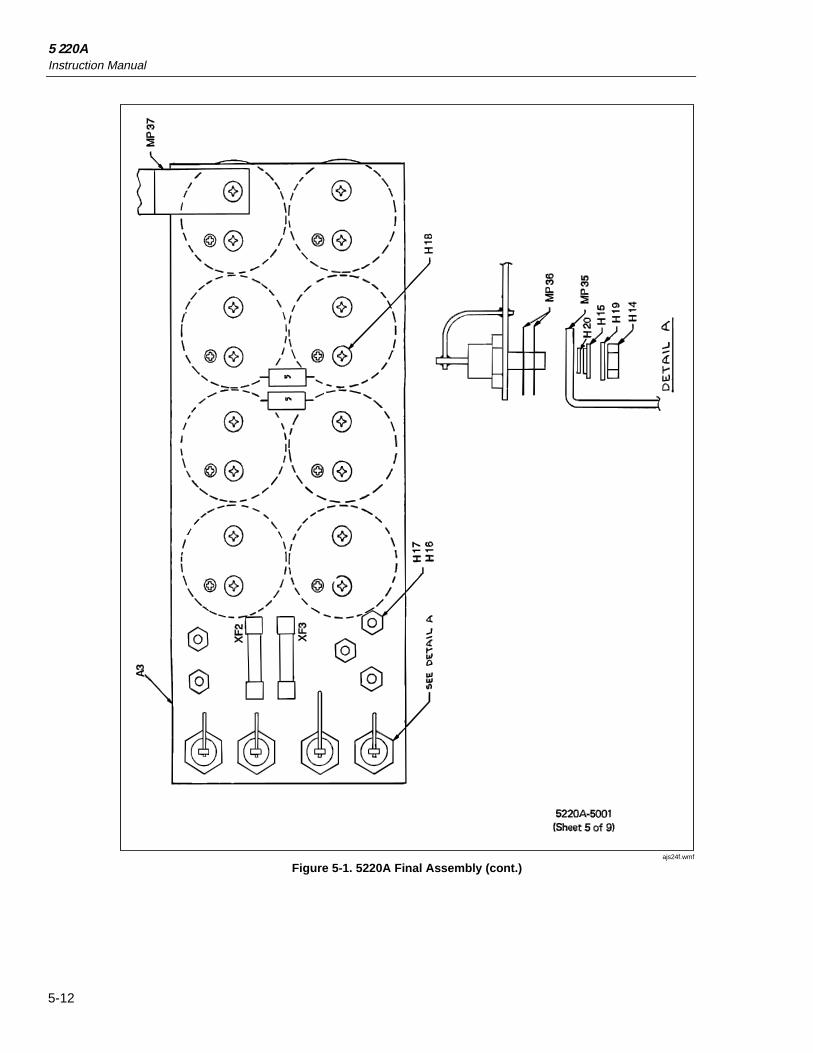
5 220AInstruction Manual
5-12
ajs24f.wmf
Figure 5-1. 5220A Final Assembly (cont.)

List of Replaceable PartsService Centers 5
5-13
ajs25f.wmf
Figure 5-1. 5220A Final Assembly (cont.)

5 220AInstruction Manual
5-14
ajs26f.wmf
Figure 5-1. 5220A Final Assembly (cont.)

List of Replaceable PartsService Centers 5
5-15
ajs27f.wmf
Figure 5-1. 5220A Final Assembly (cont.)

5 220AInstruction Manual
5-16
ajs28f.wmf
Figure 5-1. 5220A Final Assembly (cont.)

List of Replaceable PartsService Centers 5
5-17
Table 5-2. A1 Motherboard PCB Assembly
ReferenceDesignator Description
FlukePart No.
TotalQuantity
J10, J20, J30,J40, J50, J70, J90
Connector, PCB Edge, Rec., 0.150 CTR, 40 Position 422550 7
J1 Header, 1 Row, 0.156 CTR, 10 Pin 446724 1
J10, J85 Connector, PCB Edge, Rec., 0.150 CTR, 24 Position 295352 2
J80 Connector, PCB Edge, Rec., 0.150 CTR, 22 Position 459883 1
MP1 Cover, AC Switch 475681 1
MP2 Pushbutton, SML Rect. C L Repl., Green 419747 1
MP3 Pin, Single, PCB, 0.025 Sq. 267500 3
MP4 Connector, Accessory, PCB Edge, Polarizing Insert 424572 19
MP5 Bushing, Snap-In, Nylon, 0.250 ID 102996 2
MP6 Spacer, Swaged, Round, Brass, 6-32 x 0.500 284380 4
S4 Switch, On-Off 453605 1
ajs35f.wmf
Figure 5-2. A1 Motherboard PCB Assembly
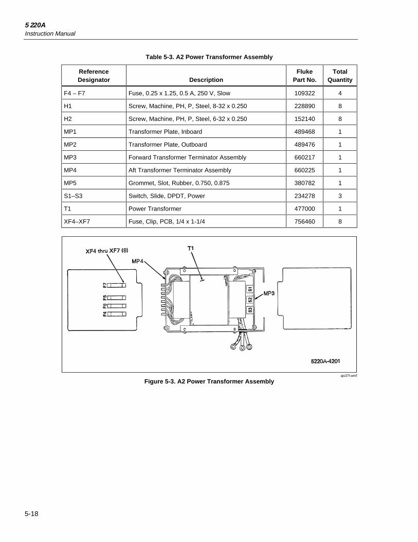
5 220AInstruction Manual
5-18
Table 5-3. A2 Power Transformer Assembly
ReferenceDesignator Description
FlukePart No.
TotalQuantity
F4 – F7 Fuse, 0.25 x 1.25, 0.5 A, 250 V, Slow 109322 4
H1 Screw, Machine, PH, P, Steel, 8-32 x 0.250 228890 8
H2 Screw, Machine, PH, P, Steel, 6-32 x 0.250 152140 8
MP1 Transformer Plate, Inboard 489468 1
MP2 Transformer Plate, Outboard 489476 1
MP3 Forward Transformer Terminator Assembly 660217 1
MP4 Aft Transformer Terminator Assembly 660225 1
MP5 Grommet, Slot, Rubber, 0.750, 0.875 380782 1
S1–S3 Switch, Slide, DPDT, Power 234278 3
T1 Power Transformer 477000 1
XF4–XF7 Fuse, Clip, PCB, 1/4 x 1-1/4 756460 8
ajs37f.wmf
Figure 5-3. A2 Power Transformer Assembly
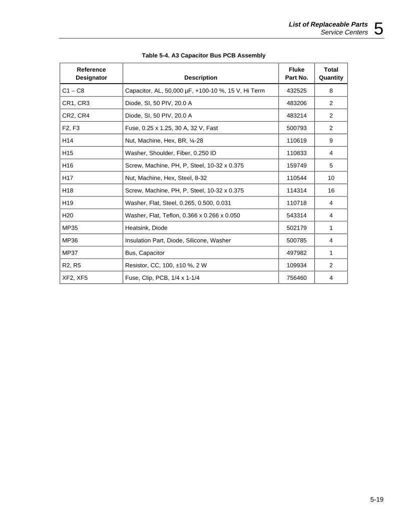
List of Replaceable PartsService Centers 5
5-19
Table 5-4. A3 Capacitor Bus PCB Assembly
ReferenceDesignator Description
FlukePart No.
TotalQuantity
C1 – C8 Capacitor, AL, 50,000 µF, +100-10 %, 15 V, Hi Term 432525 8
CR1, CR3 Diode, SI, 50 PIV, 20.0 A 483206 2
CR2, CR4 Diode, SI, 50 PIV, 20.0 A 483214 2
F2, F3 Fuse, 0.25 x 1.25, 30 A, 32 V, Fast 500793 2
H14 Nut, Machine, Hex, BR, ¼-28 110619 9
H15 Washer, Shoulder, Fiber, 0.250 ID 110833 4
H16 Screw, Machine, PH, P, Steel, 10-32 x 0.375 159749 5
H17 Nut, Machine, Hex, Steel, 8-32 110544 10
H18 Screw, Machine, PH, P, Steel, 10-32 x 0.375 114314 16
H19 Washer, Flat, Steel, 0.265, 0.500, 0.031 110718 4
H20 Washer, Flat, Teflon, 0.366 x 0.266 x 0.050 543314 4
MP35 Heatsink, Diode 502179 1
MP36 Insulation Part, Diode, Silicone, Washer 500785 4
MP37 Bus, Capacitor 497982 1
R2, R5 Resistor, CC, 100, ±10 %, 2 W 109934 2
XF2, XF5 Fuse, Clip, PCB, 1/4 x 1-1/4 756460 4

5 220AInstruction Manual
5-20
ajs38f.wmf
Figure 5-4. A3 Capacitor Bus PCB Assembly

List of Replaceable PartsService Centers 5
5-21
Table 5-5. A4 Regulator PCB Assembly
ReferenceDesignator Description
FlukePart No.
TotalQuantity
C9, C10, C16, C17 Capacitor, AL, 4700 µF, +75-20 %, 16 V 379370 4
C11, C14, C15, C18 Capacitor, TA, 22 µF, ±20 %, 25 V 357780 4
C12, C13 Capacitor, AL, 2200 µF, +75-20 %, 25 V 392720 2
CR5 – CR7 Diode, SI, Rectifier, Bridge, BV = 100 V, IO = 1.0 A 392910 3
CR8, CR9 h Diode, SI, BV = 75 V, IO = 150 mA, 500 mW 203323 2
H1 Screw, Machine, PH, P, SEMS, Steel, 4-40, 0.250 185918 4
H2 Nut, Machine, Hex, Steel, 4-40 110635 4
MP1 Heat Dissipator, PCB MTG, 1.380, 2.000, 0.500 386235 4
MP2 Cable Tie, 4.0 L, 0.100 W, 0.75 Dia. 172080 6
R4, R6, R9, R15 Resistor, CF, 100 k, ±5 %, 0.25 W 348920 4
R7, R12 Resistor, CC, 220 Ω, ±10 %, 1 W 109462 2
R8 Resistor, CF, 1 k, ±5 %, 0.25 W 343426 1
R10, R11 Resistor, CC, 1 k, ±10 %, 1 W 109371 2
R13 Resistor, CF, 18 k, ±5 %, 0.25 W 348862 1
TP1 – TP8 Terminal, Uninsulated, Feedthrough, Hole, Turret 179283 8
U1, U4 h IC, Voltage Regulator, Fixed, +5 V, 1.5 A 355107 2
U2 h IC, Voltage Regulator, Fixed, +15 V, 1.5 A 413187 1
U3 h IC, Voltage Regulator, Fixed, -15 V, 1.5 A 413179 1
VR1 h Zener, Uncompensated, 4.3 V, 5 %, 20.0 mA, 0.4 W 180455 1
h Indicates a static-sensitive part.

5 220AInstruction Manual
5-22
ajs39f.wmf
Figure 5-5. A4 Regulator PCB Assembly

List of Replaceable PartsService Centers 5
5-23
Table 5-6. A5 Preamplifier PCB Assembly
ReferenceDesignator Description
FlukePart No.
TotalQuantity
C1, C2 Capacitor, CER, 100 pF, ±2 %, 100 V, COG 512848 2
C3, C5, C6 Capacitor, CER, 0.22 µF, ±20 %, 50 V, Z5U 309849 7
C4 Capacitor, Variable,1 – 42 pF, 750 V, Glass 758029 1
C7 Capacitor, CER, 1800 pF, ±5 % 50 V, COG 528547 1
C12, C15 Capacitor, TA, 10 µF, ±20 %, 20 V 330662 2
CR1, CR2, CR6 h Diode, SI, BV = 75 V, IO = 150 mA, 500 mW 203323 3
CR3 – CR5 h Diode, SI, BV = 20.0 V, IO = 50 mA, 250 mW 375907 3
E1, E2, E3 Jumper, Wire, Non-insulated, 0.200 CTR 816090 3
H1 Screw, Machine, SEMS, PH, P, Steel, 6-32, 0.250 178533 4
K1, K2 Relay, Reed, 1 Form A, 4.5 V dc 424408 2
MP1 Spacer, Swaged, Round, Brass, 6-32 x 0.812 306804 4
MP2 Shield, Preamplifier 486001 1
MP3 Spacer, Switch Standoff, Polyethylene, 0.094 285353 2
Q1 h Transistor, SI, N-JFET, Hi-Voltage, TO-92 393314 1
Q2 h Transistor, SI, NPN, Dual, TO-5 478099 1
Q3 h Transistor, SI, NPN, Small Signal 329698 1
R1, R2 Resistor Set, 1 k; 98.5 k 502625 1
R3 Resistor, Variable, CER, 500 Ω, ±20 %, 0.5 W 267849 1
R4 Resistor, MF, 60.4 k, ±1 %, 0.125 W, 100 PPM 291419 1
R5, R7 Resistors, 301 k Set 502671 1
R6 Resistor, Variable, CER, 2 k, ±20 %, 0.5 W 267864 1
R8 Resistor, MF, 215 k, ±1 %, 0.125 W, 100 PPM 289470 1
R9 Resistor, MF, 1 k, ±, 0.125 W, 100 PPM 168229 1
R10, R20 Resistor, CF, 100 k, ±5 %, 0.25 W 348920 2
R11, R121 Resistor, MF, 100.03 k, ±0.1 %, 0.125 W, 25 PPM 291088 1
R132 Resistor, Factory Selected - 2
R14 Resistor, MF, 100k, ±1 %, 0.125 W, 100 PPM 248807 1
R15, R25 Resistor, MF, 392 Ω, ±1 %, 0.125 W, 100 PPM 260299 2
R16 Resistor, MF, 10 k, ±1 %, 0.125 W, 100 PPM 168260 1
R17, R18 Resistor, CF, 10 Ω, ±5 %, 0.25 W 340075 2

5 220AInstruction Manual
5-24
Table 5-6. A5 Preamplifier PCB Assembly (cont.)
ReferenceDesignator Description
FlukePart No.
TotalQuantity
R19 Resistor, MF, 422 Ω, ±1 %, 0.125 W, 100 PPM 288506 1
R21, R23 Resistor, CF, 1 k, ±5 %,, 0.25 W 343426 2
R22 Resistor, CF, 1.2 k, ±5 %, 0.25 W 441378 1
R24 Resistor, CF, 33k, ±5 %, 0.25 W 348888 1
TP1 – TP14 Terminal, Un-insulated, Feed-through, Hole, Turret 179283 14
U1 h IC, Array, 5 Transistors, NPN, 3 Isolated, 2Differentially Connected
248906 1
U2 h IC, OP AMP, JFET Input, TO-5 429837 1
U3 h Isolator, Opto, LED to Photo Resistor 507475 1
U4 h IC, CMOS, Hex Inverter 404681 1
h Indicates a static-sensitive part.
1. R11 and R12 are factory selected. See Table 4-4.
2. R13 may or may not be installed as factory selected. See Table 4-5.

List of Replaceable PartsService Centers 5
5-25
ajs40f.wmf
Figure 5-6. A5 Preamplifier PCB Assembly

5 220AInstruction Manual
5-26
Table 5-7. A6 Driver PCB Assembly
ReferenceDesignator Description
FlukePart No.
TotalQuantity
C1 Capacitor, Polyester, 0.027 µF, ±10 %, 250 V 267120 1
C2 Capacitor, TA, 6.8 µF, ±20 %, 35 V 363713 1
C3, C4 Capacitor, CER, 180 pF, ±10 % 1000 V, S3N 105890 2
C5 Capacitor, CER, 5000 pF, ±20 %, 100 V, Z5V 175232 1
C6 Capacitor, TA, 220 µF, ±20 %, 6 V 408682 1
C7 Capatitor, CER, 0.1 µF, ±20 %, 100 V Z5V 149146 1
CR1 h Diode, SI, N-JFET, Current Regulator, IF = 5.3 mA 334714 1
CR2 h Diode, SI, BV = 75 V, IO = 150 mA, 500 mW 203323 1
H1 Screw, Machine, PH, P, Steel, 6-32 x 1.000 114215 1
H2 Nut, Hex, Steel, 6-32 110551 1
MP1 Spacer, Round, Aluminum, 0.156 ID x 0.750 100966 1
Q1 h Transistor, SI, PNP, Small Signal 229898 1
Q2 – Q4 h Transistor, SI, NPN, Small Signal 218081 3
Q5, Q9, Q10 h Transistor, SI, PNP, Small Signal 402586 3
Q6, Q7, Q11 h Transistor, SI, N-JFET, TO-92, Switch 261578 3
Q8, Q12 h Transistor, SI, NPN, Small Signal 346916 2
R1 – R3 Resistor, CF, 1 k, ±5 %, 0.25 W 343426 3
R4, R5 Resistor, MF, 523 Ω, ±1 %, 0.125 W, 100 PPM 294835 2
R6 Resistor, Variable, CERM, 10 Ω, ±20 %, 0.5 W 344135 1
R7, R23 Resistor, CF, 100 k, ±5 %, 0.25 W 348920 2
R8 Resistor, MF, 191 Ω, ±1 %, 0.125 W, 100 PPM 325639 1
R9, R12 Resistor, CF, 560 Ω, ±5 %, 0.25 W 385948 2
R10 Resistor, 240 Ω, ±5 %, 0.25 W 376624 1
R13 Resistor, Variable, CERM, 100 Ω, ±20 % , 0.5 W 267823 1
R14, R16 Resistor, MF, 604 Ω, ±1 %, 0.125 W, 100 PPM 320309 2
R15 Resistor, MF, 383 Ω, ±1 %, 0.125 W, 100 PPM 375899 1
R17 Resistor, MF, 953 Ω, ±1 %, 0.125 W, 100 PPM 288555 1
R18, R24 Resistor, MF, 100 Ω, ±1 %, 0.125 W, 100 PPM 168195 2
R19, R25 Resistor, CF, 51 Ω, ±5 %, 0.25 W 414540 2
R20 Resistor CF, 100 Ω, ±5 %, 0.25 W 348771 1
R21, R22 Resistor, MF, 33.2 Ω, ±1 %, 0.125 W, 100 PPM 296681 2
R26, R27 Resistor, MF, 20 Ω, ±1 %, 0.125 W, 100 PPM 236844 2

List of Replaceable PartsService Centers 5
5-27
Table 5-7. A6 Driver PCB Assembly (cont.)
ReferenceDesignator Description
FlukePart No.
TotalQuantity
R28, R29 Resistor, CF, 6.8 k, ±5 %, 0.25 W 368761 2
R30, R31 Resistor, CC, 10 Ω, ±10 %, 0.5 W 108092 2
TP1 – TP4 Terminal, Un-insulated, Feed-through, Hole, Turret 179283 4
VR1, VR2 h Zener, Uncompensated, 4.3 V, 5 %, 20.0 mA, 0.4 W 180455 2
h Indicates a static-sensitive part.
ajs41f.wmf
Figure 5-7. A6 Driver PCB Assembly

5 220AInstruction Manual
5-28
Table 5-8. A7 Output PCB Assembly
ReferenceDesignator Description
FlukePart No.
TotalQuantity
H1 Screw, Machine, PH, P, Steel, 4-40 x 0.375 152124 2
H2 Washer, Lock, Internal, Steel, #4 110403 2
H3 Nut, Hex, S. Steel, 4-40 147611 2
H4 Screw, Machine, PH, P, Steel, 6-32 x 0.250 152140 2
H5 Screw, Machine, PH, P, Steel, 6-32 x 0.750 114223 8
H6 Washer, Lock, Internal, Steel #6 110338 1
H7 Nut, Hex, Steel, 6-32 110551 1
H8 Screw, Machine, PH, P, Steel, 8-32 x 0.35 114124 8
H9 Nut, Macine, Hex, Steel, 8-32 110544 2
H10 Screw, Machine, PH, P, Steel, 4-40 x 0.312 152116 1
MP1 Output, PCB Bracket 489567 1
MP2 Fin, Heatsink 489880 1
MP3 Plate, Temperature Sense 489898 1
MP4 Bus, Output PCB 502161 2
MP5 Output Chamber 485961 1
MP6 Defector Fin, Heatsink 489508 1
MP7 Spacer, Swaged, Hex, Brass, 6-32 x 0.625 181727 2
MP8 Spacer, Swaged, Round, Brass, 6-32 x 0.187 351882 8
MP9 Insulated Part, Transistor, Aluminum, TO-3 477802 4
MP10 Socket, Single, PCB, For 0.018 – 0.040 Pin 348201 8
MP11 Heat Dissipator, W/BEO Washer, TO-5 407262 1
MP12 Space, Transistor Mount, DAP 152207 1
MP13 Washer, Flat, Nylon, 0.257 ID x 0.500 x 0.093 682385 1
MP14 Plastic Part, Hole Plug, Polyethylene, 0.312 187799 2
MP15 Washer, Shoulder, Nylon, 0.113, 0.345 485417 3
MP16 Insulated Part, Transistor, Film, TO-220 412809 1
Q101 h Transistor, SI, BV = 45 V, 27 W, TO-220 325753 1
Q102 h Transistor, SI, BV = 45 V, 30 W, TO-220 325761 1
Q103, Q104 h Transistor, SI, BV = 60 V, 200 W, TO-3 483222 2
Q105, Q106 h Transistor, SI, PNP, Small Signal 483230 2
Q107 Resistor, CF, 1 k, ±5 %, 0.25 W 402586 1
R101 – R107 Resistor, CF, 1 k, ±5 %, 0.25 W 343426 7
R108, R109 Resistor, CC, 5.1 Ω, ±5 %, 0.5 W 177147 2
R110 – R113 Resistor, 0.086 Ω, ±1 %, 4-Terminal, 10 W, 50 PPM 490771 4
R114, R115 Resistor, WW, 2.4 Ω, ±5 %, 2 W 219337 2
S101 Thermo, NO230±8F, NC200±8F, 15 A/120 V ac 344002 1
TP1 – TP7 Terminal, Un-insulated, Feed-through, Hole, Turret 179283 7
XQ101, XQ102 Socket, Transistor, 3-Pin 402958 2
h Indicates a static-sensitive part.

List of Replaceable PartsService Centers 5
5-29
ajs42f.wmf
Figure 5-8. A7 Output PCB Assembly

5 220AInstruction Manual
5-30
ajs43f.wmf
Figure 5-8. A7 Output PCB Assembly (cont.)

List of Replaceable PartsService Centers 5
5-31
Table 5-9. A8 Analog Control PCB Assembly
ReferenceDesignator Description
FlukePart No.
TotalQuantity
C1 Capacitor, CER, 0.10 µF, ±20 %, 50 V, X7R 853650 1
C2 Capacitor, Polyester, 0.22 µF, ±10 %, 100 V 436113 1
C3 Capacitor, TA, 0.68 µF, ±10 %, 35 V 182790 1
CR1 – CR10 h Diode, SI, BV = 20.0 V, IO = 50 Machine, Selected IR 348117 10
CR11 h Diode, SI, BV = 75.0 V, IO = 150 Machine, 500 mW 203323 1
Q1, Q3 h Transistor, SI, PNP, Small Signal 195974 2
Q2, Q4 h Transistor, SI, NPN, Small Signal 218396 2
R1, R2 Resistor, MF, 100 k, ±1 %, 0.125 W, 100 PPM 248807 2
R3 Resistor, CF, 51 k, ±5 %, 0.25 W 376434 1
R4, R6, R7, R16 –R19, R25, R28,R29, R32
Resistor, CF, 10 k, ±5 %, 0.25 W 348839 11
R5, R10, R27, R31,R35 – R42
Resistor, CF, 100 k, ±5 %, 0.25 W 348920 12
R8 Resistor, CF, 82 k, ±5 %, 0.25 W 348912 1
R9 Resistor, Variable, CER, 100 k, ±10 %, 0.5 W 288308 1
R11 Resistor, CF, 300 k, ±5 %, 0.25 W 441535 1
R12, R24, R43 Resistor, CF, 1 k, ±5 %, 0.25 W 343426 3
R13, R14 Resistor, MF, 10 k, ±1 %, 0.125 W, 100 PPM 168206 2
R15 Resistor, CF, 5.1 k, ±5 %, 0.25 W 368712 1
R20 Resistor, CF, 9.1 k, ±5 %, 0.25 W 441691 1
R21 Resistor, Variable, CER, 5 k, ±10 %, 0.5 W 288282 1
R22 Resistor, CF 1.1 k, ±5 %, 0.25 W 348797 1
R23 Resistor, CF, 390 k, ±5 %, 0.25 W 742475 1
R26, R30 Resistor, CF, 22 k, ±5 %, 0.25 W 348870 2
R33 Resistor, CF, 1.2 k, ±5 %, 0.25 W 441378 1
TP1 – TP5, TP7 –TP13
Terminal, Un-insulated, Feed-through, Hole, Turret 179283 12
U1, U2 h IC, Op Amp, Quad, 14-Pin DIP 402669 2
U3 h IC, LSTTL, Hex Inverter w/Schmitt Trigger 483180 1
VR1, VR2 h Zener, Uncompensated, 6.8 V, 10 %, 1.0 Machine, 0.4 W 187195 2
h Indicates a static-sensitive part.

5 220AInstruction Manual
5-32
ajs44f.wmf
Figure 5-9. A8 Analog Control PCB Assembly

List of Replaceable PartsService Centers 5
5-33
Table 5-10. A9 Front Panel PCB Assembly
ReferenceDesignator Description
FlukePart No.
TotalQuantity
C1 Capacitor, CER, 0.22 µF, ±20 %, 50 V, Z5U 309849 1
DS1 – DS9 LED, Red, PCB mount, Luminous Intensity = 0.5 MCD 369777 9
MP1 Cover, Pushbutton, Switch 401299 3
MP2 Switch Part, SPST, Spring 414516 3
MP3 Switch Part, SPST, Fixed Contact 416875 3
MP4 Pushbutton-Square-, Dark Putty Grey 406728 3
R1 – R9 Resistor, CF, 220 Ω, ±5 %, 0.25 W 342626 9
S1 – S3 Actuator, Switch 412106 3
TP1 – TP2 Terminal, Un-insulated, Feed-through, Hole, Turret 179283 2
ajs29f.wmf
Figure 5-10. A9 Front Panel PCB Assembly
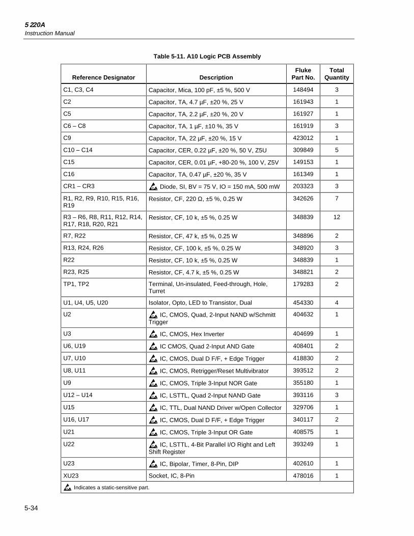
5 220AInstruction Manual
5-34
Table 5-11. A10 Logic PCB Assembly
Reference Designator DescriptionFluke
Part No.Total
Quantity
C1, C3, C4 Capacitor, Mica, 100 pF, ±5 %, 500 V 148494 3
C2 Capacitor, TA, 4.7 µF, ±20 %, 25 V 161943 1
C5 Capacitor, TA, 2.2 µF, ±20 %, 20 V 161927 1
C6 – C8 Capacitor, TA, 1 µF, ±10 %, 35 V 161919 3
C9 Capacitor, TA, 22 µF, ±20 %, 15 V 423012 1
C10 – C14 Capacitor, CER, 0.22 µF, ±20 %, 50 V, Z5U 309849 5
C15 Capacitor, CER, 0.01 µF, +80-20 %, 100 V, Z5V 149153 1
C16 Capacitor, TA, 0.47 µF, ±20 %, 35 V 161349 1
CR1 – CR3 h Diode, SI, BV = 75 V, IO = 150 mA, 500 mW 203323 3
R1, R2, R9, R10, R15, R16,R19
Resistor, CF, 220 Ω, ±5 %, 0.25 W 342626 7
R3 – R6, R8, R11, R12, R14,R17, R18, R20, R21
Resistor, CF, 10 k, ±5 %, 0.25 W 348839 12
R7, R22 Resistor, CF, 47 k, ±5 %, 0.25 W 348896 2
R13, R24, R26 Resistor, CF, 100 k, ±5 %, 0.25 W 348920 3
R22 Resistor, CF, 10 k, ±5 %, 0.25 W 348839 1
R23, R25 Resistor, CF, 4.7 k, ±5 %, 0.25 W 348821 2
TP1, TP2 Terminal, Un-insulated, Feed-through, Hole,Turret
179283 2
U1, U4, U5, U20 Isolator, Opto, LED to Transistor, Dual 454330 4
U2 h IC, CMOS, Quad, 2-Input NAND w/SchmittTrigger
404632 1
U3 h IC, CMOS, Hex Inverter 404699 1
U6, U19 h IC CMOS, Quad 2-Input AND Gate 408401 2
U7, U10 h IC, CMOS, Dual D F/F, + Edge Trigger 418830 2
U8, U11 h IC, CMOS, Retrigger/Reset Multivibrator 393512 2
U9 h IC, CMOS, Triple 3-Input NOR Gate 355180 1
U12 – U14 h IC, LSTTL, Quad 2-Input NAND Gate 393116 3
U15 h IC, TTL, Dual NAND Driver w/Open Collector 329706 1
U16, U17 h IC, CMOS, Dual D F/F, + Edge Trigger 340117 2
U21 h IC, CMOS, Triple 3-Input OR Gate 408575 1
U22 h IC, LSTTL, 4-Bit Parallel I/O Right and LeftShift Register
393249 1
U23 h IC, Bipolar, Timer, 8-Pin, DIP 402610 1
XU23 Socket, IC, 8-Pin 478016 1
h Indicates a static-sensitive part.

List of Replaceable PartsService Centers 5
5-35
ajs30f.wmf
Figure 5-11. A10 Logic PCB Assembly

5 220AInstruction Manual
5-36
Table 5-12. A11 MIS Bus Interface PCB Assembly
ReferenceDesignator Description
FlukePart No.
TotalQuantity
C1 Capacitor, TA, 4.7 µF, ±20 %, 25 V 161943 1
C2 Capacitor, TA, 22 µF, ±20 %, 15 V 423012 1
C3, C4 Capacitor, CER, 0.22 µF, ±20 %, 50 V, Z5U 309849 2
CR1 h Diode, SI, BV = 75.0 V, IO = 150 mA, 500 mW 203323 1
H1 Screw, Machine, PH, P, SEMS, Steel, 4-40, 0.250 185918 2
J71 Connector, Micro-Ribbon, REC, PCB, 24 Position 441337 1
MP1 Connector ACC, Micro-Ribbon, Latch 412700 2
MP2 Connector ACC, Micro-Ribbon, Spring 412718 2
MP3 Spacer, Swaged, Round, Brass, 4-40 x 0.187 335604 2
MP4 Spacer, Swaged, Round, Brass, 6-32 x 0.570 261875 1
R1 – R12 Resistor, CF, 10 k, ±5 %, 0.25 W 348839 12
R14 – R22 Resistor, CF, 1 k, ±5 %, 0.25 W 343426 9
R23 Resistor, CF, 47 k, ±5 %, 0.25 W 348896 1
TP1 – TP2 Terminal, Un-insulated, Feed-through, Hole, Turret 179283 2
U1 h IC, CMOS, Quad D F/F, + Edge Trigger, w/Clear 452912 1
U2 – U7 h IC, LSTTL, Quad 2-Input NAND Gate 394205 2
U3 h IC, CMOS, Hex Inverter 404699 1
U4 h IC, CMOS, Quad 2-Input NAND Gate 418509 1
U5 h IC, CMOS, Triple 3-Input NAND Gate 418244 1
U6 h IC, LSTTL, Quad 2-Input NAND Gate 393116 1
h Indicates a static-sensitive part.

List of Replaceable PartsService Centers 5
5-37
ajs31f.wmf
Figure 5-12. A11 MIS Bus PCB Assembly
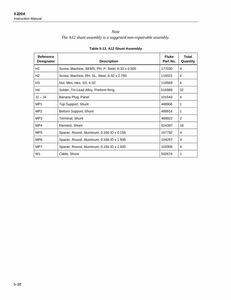
5 220AInstruction Manual
5-38
NoteThe A12 shunt assembly is a suggested non-repairable assembly.
Table 5-13. A12 Shunt Assembly
ReferenceDesignator Description
FlukePart No.
TotalQuantity
H1 Screw, Machine, SEMS, PH, P, Steel, 6-32 x 0.500 177030 4
H2 Screw, Machine, RH, SL, Steel, 6-32 x 2.750 115022 4
H3 Nut, Mini, Hex, SS, 6-32 110569 4
H4 Solder, Tin-Lead Alloy, Preform Ring 516989 32
J1 – J4 Banana Plug, Panel 101543 4
MP1 Top Support, Shunt 489906 1
MP2 Bottom Support, Shunt 489914 1
MP3 Terminal, Shunt 489922 2
MP4 Element, Shunt 524397 16
MP5 Spacer, Round, Aluminum, 0.156 ID x 0.156 157792 4
MP6 Spacer, Round, Aluminum, 0.156 ID x 1.500 104257 4
MP7 Spacer, Round, Aluminum, 0.156 ID x 1.000 102905 4
W1 Cable, Shunt 502674 1

List of Replaceable PartsService Centers 5
5-39
ajs32f.wmf
Figure 5-13. A12 Shunt Assembly

5 220AInstruction Manual
5-40
Table 5-14. A13 Output Termination PCB Assembly
ReferenceDesignator Description
FlukePart No.
TotalQuantity
C1 Capacitor, CER, 0.025 µF, 20 %, 100 V, Z5W 168435 1
C2 Capacitor, CER, 0.1 µF, +80-20 %, 25 V, Z5U 369199 1
R1 Resistor, MF, 40.2, ±1 %, 0.125 W, 100 PPM 245373 1
R2 Resistor, CF, 10 Ω, ±5 %, 0.25 W 340075 1
ajs33f.wmf
Figure 5-14. A13 Output Termination PCB

List of Replaceable PartsService Centers 5
5-41
Table 5-15. A14 Extender PCB Assembly
ReferenceDesignator Description
FlukePart No.
TotalQuantity
H1 Screw, Machine, SEMS, PH, P, Steel, 6-32, 0.250 178533 4
H2 Rivet, S-Tub, Oval, Steel, 0.118 x 0.218 103606 2
J1 Connector, PCB Edge, REC, 0.150 CTR, 40 Position 422550 1
J2 Connector, ACC, PCB Edge, Polarizing Insert 424572 1
MP1 Bracket, Right Angle, Tapped, Brass, 6-32 404525 4
ajs34f.wmf
Figure 5-15. A14 Extender PCB Assembly

5 220AInstruction Manual
5-42

6-1
Section 6Option and Accessory Information
6-1. IntroductionThis section of the manual documents the options and accessories available for use withthe 5220A. Currently, there are no options, and the accessories are limited to a choice oftwo rack-mounting kits and a precision current shunt for calibration purposes. Each isdescribed in the following accessories subsection.
6-2. Accessories
6-3. Rack Mounting Kit (M08-205-600)The 5220A can be rack mounted in a standard 19-inch equipment rack using RackMounting Kit M08-205-600. Use the following procedure to install the kit:
1. Peel off the name plate decals from the front side corners of theinstrument.
2. Remove the front corner screws that match the hole pattern in the rack mounting ears(see Figure 6-1).
3. Attach the rack mounting ears to the front corners of the unit using the screwssupplied in the rack mounting kit.

5 220AInstruction Manual
6-2
ajs45f.wmf
Figure 6-1. Rack Mounting Kit

Option and Accessory InformationAccessories 6
6-3
6-4. Rack Slide Kit (M00-280-610)The 5220A can be rack mounted in a 24-inch deep equipment rack using the Rack SlideKit, model M00-280-610. Use the following procedure to install the kit:
1. Remove the horizontal side trim decal from both sides of the instrument.
2. Refer to Figure 6-2. Using the screws supplied with the kit, attach the chassis section(B) of the slide kit to each side of the unit. Use the center row of mounting holes.
3. Install the cabinet section (D) of the center section (C) in the equipment rack.
4. Pull the center section of the slide out through the front of the equipment rack until itlocks in the extended position.
5. Depress the spring locks on the chassis section (B) and join sections B and C.
6. Push the instrument into the equipment rack and then pull it out to the extendedposition. The spring locks should limit the rack slide travel.
6-5. Precision Y5020A Current ShuntThe Model Y5020A is a precision, high-current shunt recommended for use in calibratingthe Model 5220A Transconductance Amplifier. An instruction manual is suppled with theunit.

5 220AInstruction Manual
6-4
ajs46f.wmf
Figure 6-2. Rack Slide Kit

7-1
Chapter 7Schematic Diagrams

5220AInstruction Manual
7-2
5220A-1001 (Sheet 1 of 2)
ajs47f.wmf
Figure 7-1. Interconnect Diagram
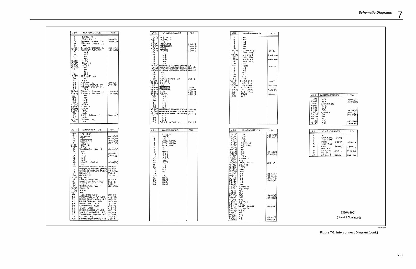
Schematic Diagrams 7
7-3
ajs48f.wm
Figure 7-1. Interconnect Diagram (cont.)

5220AInstruction Manual
7-4
ajs49f.wmf
Figure 7-2. Chassis Wiring

Schematic Diagrams 7
7-5
ajs50f.wmf
Figure 7-2. Chassis Wiring (cont.)

5220AInstruction Manual
7-6
ajs51f.wmf
Figure 7-3. Power Supply

Schematic Diagrams 7
7-7
ajs52f.wmf
Figure 7-3. Power Supply (cont.)
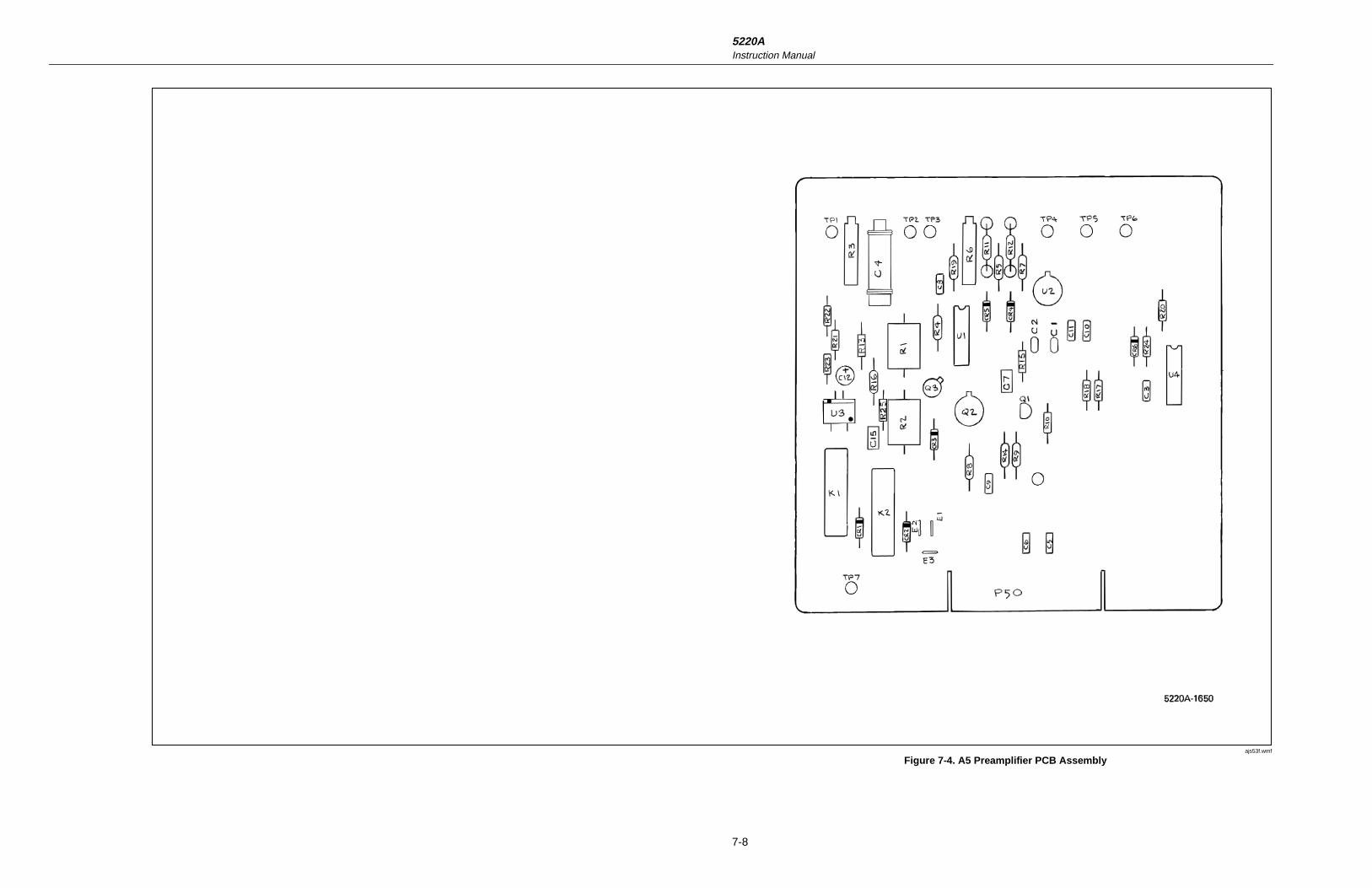
5220AInstruction Manual
7-8
ajs53f.wmf
Figure 7-4. A5 Preamplifier PCB Assembly

Schematic Diagrams 7
7-9
ajs54f.wmf
Figure 7-4. A5 Preamplifier PCB Assembly (cont.)

5220AInstruction Manual
7-10
ajs55f.wmf
Figure 7-5. A6 Driver and A7 Output PCB Assemblies
Schematic Diagrams 7
7-11
ajs56f.wmf
Figure 7-5. A6 Driver and A7 OutputPCB Assemblies (cont.)

5220AInstruction Manual
7-12
ajs57f.wmf
Figure 7-6. A8 Analog Control PCB Assembly

Schematic Diagrams 7
7-13
ajs58f.wmf
Figure 7-6. A8 Analog Control PCB Assembly (cont.)

5220AInstruction Manual
7-14
ajs59f.wmf
Figure 7-7. A9 Front Panel PCB Assembly

Schematic Diagrams 7
7-15
ajs60f.wmf
Figure 7-7. A9 Front Panel PCB Assembly (cont.)

5220AInstruction Manual
7-16
ajs61f.wmf
Figure 7-8. A10 Logic PCB Assembly
Schematic Diagrams 7
7-17
ajs62f.wmf
Figure 7-8. A10 Logic PCB Assembly (cont.)

5220AInstruction Manual
7-18
ajs63f.wmf
Figure 7-9. A11 MIS Bus Interface PCB Assembly

Schematic Diagrams 7
7-19
ajs64f.wmf
Figure 7-9. A11 MIS Bus InterfacePCB Assembly (cont.)

5220AInstruction Manual
7-20