Embed Size (px)
Citation preview

Instruction Manual Model 175
Autoranging Multimeter
01983, Keithley Instruments, Inc. Cleveland, Ohio, U.S.A.
Document Number 175-901-01

SPECIFICATIONS

TABLE OF CONTENTS
Paragraph Title Peg.3
1.1 1.2 1.3 1.4 1.5 1.6 1.7 1.8
‘SECTION l-GENERAL INFORMATION Introduction ............................. Getting Started .......................... Unpacking and Inspection ................. Specifications ........................... Warranty Information ..................... Manual Addenda ......................... Safety Symbols and Terms. ................ Optional Accessories. .....................
.................
.................
.................
.................
.................
.................
.................
.................
......
......
......
......
......
......
......
......
..........
..........
..........
..........
..........
..........
......
......
......
1-l 1~1 l-l 1-2 l-2 1-2 1-2 1-2
2-1 2-1
2.1 2.2 2.3 2.3.1 2.3.2 2.3.3 2.4 2.4.1 2.4.2 2.4.3 2.4.4 2.5 2.6 2.6.1 2.6.2 2.7 2.7.1 2.7.2 2.7.3 2.7.4 2.7.5 2.7.6 2.7.7 2.7.8 2.7.9 2.7.10 2.7.11 2.8 2.8.1 2.8.2 2.8.3 2.8.4
3.1 3.2 3.3 3.4 3.5 3.5.1 3.5.2 3.5.3 3.5.4 3.5.5
SECTION 2-BENCH OPERATION Introduction .................................... High Energy Circuit Precautions. ................... Preparation for Use ..............................
LinePower.. ................................. Battery Pack Power. ........................... Batten, Charging ..............................
Front Panel Familiarization ........................ Display ...................................... Front Panel Controls ........................... Input Terminals ............................... Current Fuse Replacement ......................
Error Messages ................................. Operating Conditions ............................
Environmental Conditions. ...................... Maximum Allowable Input ......................
Basic Bench Measurements ....................... Power-Up .................................... Relative Mode ................................ DC Voltage Measurements. ..................... TRMS AC Voltage Measurements. ............... Resistance Measurements ...................... Current Measurements (DC or TRMS AC) ......... AC Plus DC Measurements ..................... dl3 Measurements ............................. dl3 Measurement Considerations and Applications MINtMAX and 100 Point Logger Operation ....... DiodeTest ...................................
TRMS Consideration ............................. AC Voltage Offset ............................. TRMS Measurements Comparison ............... Crest Factor .................................. Extended Frequency Response ..................
SECTION 3-PERFORMANCE VERIFICATION Introduction .................................... Environmental Conditions ......................... Recommended Test Equipment. ................... Initial Conditions ................................ Verification Procedure ............................
DC Voltage Accuracy Check .................... AC Voltage Accuracy Check .................... Resistance Accuracy Check ..................... DC Current Accuracy Check .................... AC Current Accuracy Check ....................
..........
..........
..........
..........
..........
..........
..........
..........
..........
..........
......
......
......
......
... ..
......
2~1 2-l 2-l 2-1 2~2 2-2 2-2 2-3 2-3 2-3 2-3 2-3 2-4 2-4 2-4 2-4 2-4
2-9 2-9 2-9
3-2 3-2 3-2 3-3

TABLE OF CONTENTS
Paragraph Title Page
4.1 4.2 4.3 4.3.1 4.3.2 4.3.3 4.3.4 4.3.5 4.3.6 4.4 4.4.1 4.4.2 4.4.3 4.4.4 4.5 4.6 4.7
5.1 5.2 5.3 5.4 5.4.1 5.4.2 5.4.3 54.4 5.4.5 5.5 5.6 5.7 5.7.1 5.7.2 5.7.3 5.7.4 5.7.5 5.7.6 5.7.7 5.7.8
6.1 6.2 6.3 6.4 6.5
SECTION 4-THEORY OF OPERATION Introduction .................................................................................. Overall Functional Description ................................................................... AnalogCircuitry ...............................................................................
Multiplexer ................................................................................. InputBufferAmplifier ........................................................................ ~2VRefetenceSource ........................................................................ AiDConverter .............................................................................. Input Signal Conditioning ..................................................................... ACConverter ...............................................................................
DigitalCircuitry ............................................................................... Microcomputer ............................................................................. AddressDecoding ........................................................................... PIA ....................................................................................... Display Board ...............................................................................
DigitalCalibration ............................................................................. PowerSupply ................................................................................ Model17588atten/Option ......................................................................
SECTION 5-MAINTENANCE Introduction .................................................................................. Top Cover Removal/Installation ................................................................. Batten/ Pack (Model 1768) Installation ............................................................. Troubleshooting ..............................................................................
RecommendedTestEquipment ................................................................ SelfDiagnosticProgram ...................................................................... PowerSupplyChecks ........................................................................ AfDConverterandDisplay ................................................................... Signalconditioning ..........................................................................
LineFuseReplacement ......................................................................... Special Handling of Static Sensitive Devices ....................................................... Front Panel Calibration .........................................................................
Recommended Calibration Equipment .......................................................... CalibrationJumper.. ........................................................................ Environmentalconditions ..................................................................... DC Voltage Calibration .......................................................................
ACVoltageCalibration ......................................................................... Resistance Calibration. ....................................................................... Frequencycompensation .....................................................................
CalibrationStorage ............................................................................
SECTION 6-REPLACEABLE PARTS Introduction .................................................................................. ReplaceableParts ............................................................................. Orderinginformation ........................................................................... FactoryService.. ............................................................................. Component Location Drawings and Schematic Diagrams ...........................................
4-l 4-1 4-l 4-2 4-2 4-2 4-2 4-3 4-4 45 4-5 4-5 4-5 4-5 4-5 4-5 4-5
5-1 5-l 5-l 5-l 5-l 5-2 5-4 5-4 5-4 5-6 5-6 5-7 5-7 5-7 5-7 5-7
5-8 5-8 59
6-l 6-l 6-l 6-l 6-l

LIST OF ILLUSTRATIONS
Figure 2-1 2-2 2-3 2-4 2-5 2-6 2-7 4-1 4-2 4-3 4-4 4-5 4-6 5-l 5-2 6-l 6-2 6-3 6-4 6-5 6-6 6-7 6-8
Title Model175FrontPanel .................................................. DC Voltage Measurements. .............................................. TAMS AC Voltage Measurements. ........................................ Resistance Measurements ............................................... Current Measurements Between 2000mA and 20A. .......................... Current Measurements up to 2000mA ..................................... Model 175 Typical AC Frequency Response ................................
Simplified Block Diagram ................................................ Simplified Schematic of the Multiplexer .................................... Simplified Schematic of the Input Buffer Amplifier ........................... AIDConverter ......................................................... Resistance Measurements Ratiometric Technique. ........................... Simplified Schematics of Ohms Circuitry ................................... Segment Identification .................................................. CalibrationJumper.. ................................................... Modell75ExplodedView ................................................ Model 175 Display Assembly ............................................. Display Board, Component Location Drawing, Dwg. No. 175-110. .............. Model 1758 Battery Pack, Component Location Drawing, Dwg. No. 1755.100 .... Mother Board, Component Location Drawing, Dwg. No. 175-100 .............. Mother Board, Schematic Diagram, Dwg. No. 175.106 ....................... Display Board, Schematic Diagram, Dwg. No. 175.116 ....................... Model 1758 Battery Pack, schematic Diagram, Dwg. No. 1758-106 .............
Page 2-2 2-5 2-5 2-6 2-6 2-6
2.11 4-l 4-2 4-2 4-3 4-4 4-4 5-2 5-9 6-2 6-3 6-9
811 6-13 6-17 6-21 6-23
iii

Table 2-l 2-2 2-3 2-4 2-5 2-6 3-l 3-2 3-3 3-4 3-5 5-l 5-2 5-3 5-4 5-5 5-6 5-7 5-8 5-9 5-10 6-l 6-2 6-3 6-4
LIST OF TABLES
Title ErrorMessages ..................................... Model 175 Maximum Allowable Inputs .................. dB Specifications for DC Volts (6OOL1 Refl ............... d8 Specifications for AC Volts (6OOfl Refl ............... Levels for Other Reference Impedances ................. Comparison of Average and TRMS Meter Readings ....... Equipment Specifications. ............................ Limits for DC Voltage Verification ...................... Limits for AC Voltage Verification ...................... Limits for Resistance Verification ....................... Limits for DC Current Verification ...................... Recommended Troubleshooting Equipment. ............. Troubleshooting Modes .............................. Power Supply Checks. ............................... A/D Converter Checks ............................... Display Board Checks.. .............................. Static Sensitive Devices .............................. Recommended Calibration Equipment .................. DC Voltage Calibration ............................... AC Voltage Calibration ............................... Resistance Calibration. ............................... MotherBoard,PartsList .............................. Display Board, Parts List. ............................. Model 1758 Battery Pack, Parts List .................... Model 1758 Spare Pats List. ..........................
......
......
......
......
......
......
......
......
......
......
......
......
......
......
......
......
......
......
......
......
......
......
......
......
......
......
......
......
......
......
......
......
......
......
......
......
......
......
......
......
......
......
......
......
......
......
......
......
......
......
......
......
......
......
......
......
......
......
......
......
......
......
......
......
......
......
......
......
......
......
......
......
......
......
......
......
......
......
......
......
......
......
......
......
......
......
......
......
......
......
......
......
......
......
......
......
......
......
......
......
......
......
......
......
......
......
......
......
......
......
......
......
......
......
......
......
......
......
......
......
......
......
Page
iv

SAFETY PRECAUTIONS
The following safety precautions should be observed before operating the Model 175.
This instrument is intended for use by qualified personnel who recognize shock hazards and are familiar with the safety precautions re- quired to avoid possible injury. Read over the manual carefully before operating this instrument.
Exercise extreme caution when a shock hazard is present at the instru- ment’s input. The American National Standards Institute (ANSI) states that a shock hazard exists when voltage levels greater than 30V rms or 42.4V peak are present. A good safety practice is to expect that a hazardous voltage is present in any unknown circuit before measuring.
Inspect the test leads for possible wear, cracks or breaks before each use. If any defects are found, replace with test leads that have the same measure of safety as those supplied with the instrument.
For optimum safety do not touch the test leads or the instrument while power is applied to the circuit under test. Turn the power off and discharge all capacitors, before connecting or disconnecting the instru- ment.
Do not touch any object which could provide a current path to the common side of the circuit under test or power line (earth) ground. Always make measurements with dry hands while standing on a dry, insulated surface, capable of withstanding the voltage being measured.
Exercise extreme safety when testing high energy power circuits (AC line or mains, etc.). Refer to the operation section.
Do not exceed the instrument’s maximum allowable input as defined in the specifications and operation section.

MODEL 175 AUTORANGING DMM
Features:
04% Digit LCD Display *Fast Autoranging *Bench or Portable *Digital Calibration l lOO Point Data Logger l 10~V/10mW10nA Sensitivity ~0.03% Basic DCV Accuracy l TRMS AC
l dBm/Relative Functions l Min/Max Reading Hold *Safety Input Jacks *lOA Capability l lOOkHz Specified AC Bandwidth
Options:
*Model 1758 Rechargeable Battery Pack *Model 1753 IEEE-488 Interface

SECTION 1 GENERAL INFORMATION
1.1 INTRODUCTION
This instruction manual contains the necessary information for operating and maintaining the Model 175 Autoranging Multimeter and the Model 1758 Rechargeable Battery Pack. The information is divided into the following sections:
Section 1 contains general information and provides guidelines for using this manual. Important safety infor- mation is also presented here. Section 2 contains detailed bench operation information for the Model 175.
Section 3 contains the information needed to verify the accuracy of the Model 175. Performance verification can be done upon receipt of the unit or whenever the basic accuracy is in question. For the more technically oriented, information on theory of operation, and maintenance and servicing is contained in Section 4 through 6.
NOTE The Model 1753 IEEE-488 interface comes sup- plied with its own instruction manual.
1.2 GE-iTING STARTED
Perform the following steps in sequence to acquaint yourself auicklv and safelv with the basic operation of the Model 175.
Verify that the Model 175 was not damaged in transit, es explained in paragraph 1.3.
Carefully read the safety precautions and warnings found preceding this section and the first two sections (General Information and Bench Operation) of this manual.
Referring to paragraph 2.3.1 (Line Power) set the line voltage switch and plug the power cord into a properly grounded outlet. If the optional battery pack is installed the charge circuitry will be activated. Acquaint yourself with the controls and display of the Model 175 as follows: A. Turn on the Model 175 by pressing in the ON/OFF
pushbutton. All of the zeroee will be displayed briefly.
B. Connect the supplied test leads to the VOLTS/OHMS/mA and COM input jacks, and short them together.
C. Select AC volts and autoranging by pressing in the AC/DC, V and AUTO pushbuttons. The AC, mV and AUTO annunciators will be displayed. Pressing any of the other range pushbuttons will put the Model 175 in manual ranging es indicated by the absence of the AUTO annunciator.
D.
E.
F.
G.
H.
I.
Select DC volts by releasing (outi the AC DC pushbutton (V still selected]. The AC annunciator will turn off. Select autoranging ohms by pressing in the !! pushbutton (DC still selected) and AUTO pushbutton. The n annunciator will turn on. Press the AC:DC pushbutton in (AC selected) and note the “Err” message indicating that this is an invalid mode.
Select AC or DC current by setting the AC DC pushbutton accordingly and pressing I,? ihe A pushbutton. The annunciator that reflects the selected range will turn on. Note that current will not autorange and that the 10 AMPS and COM input jacks must be used on the 10A range. Select dB by placing the Model 175 in AC or DC volts and pressing the dB pushbutton. The dB annunc~etor will turn on. Press the dB button again fo take the Model 175 out of the dB measurement mode. REL (relative) can be used with any measurement furw tion: volts, ohms, amps or dB. For example, place the Model 175 in ohms and autorange. The display wll read approximately 00.141!, which is the test lead resistance. Press the REL pushbutton. The REL any nunciator will turn on and the display will now reed OO.OOI2. The relative level of 0.1411 will be subtracted from all subsequent ohm measurements. Press the REL pushbutton a second time to cancel the REL level.
To activate the 100 point DATA LOGGER with MIN/MAX, press and hold in the STOiCLR pushbut- ton. When the reading rate A = 0 is displayed let go of the button, The ST0 annunciator will turn on Press the RCL pushbutton and the last data point will be displayed briefly followed by the reading (data]. Other data points can be displayed by holding in the RCL but- ton. Turn off the DATA LOGGER by pressing the STOlCLR pushbutton again.
5. When you are comfortable with the controls of the Model 175, go on and make the desired meaeurements using Section 2, Bench Operation es a guide.
1.3 UNPACKING AND INSPECTION
The Model 175 Bench DMM was carefully inspected, both mechanically and electrically, before shipment. Upon recelv ing the Model 175, carefully unpack all items from the ship- ping carton and check for any obvious signs of physical damage that might have occurred during shipment. Report the damage to the shipping agent immediately. Retain the
1-l

original packing materials in case reshipment becomes necessan/. The following items are included with every Model 175 order:
*Model 175 Autoranging Multimete! *Model 175 instruction Manual ‘Model 1751 Safety Test Lead *Additional accessories as ordered.
1.4 SPECIFICATIONS
Detailed Model 175 specifications may be found immediately preceding the table of contents of this manual.
1.5 WARRANTY INFORMATION
Warranty information may be found on the inside back cover of this manual. Should it be necessary to exercise thewarran- ty, contact your Keithley representative or the factory to determine the correct course of action. Keithley Instruments maintains service facilities in the United States, West Germany, Great Britain, France, the Netherlands. Switzerland and Austria. Information concerning the applica- tion, operation or service of your instrument may be directed to the applications engineer at any of theses locations. Check the inside front cover of this manual for addresses.
1.6 MANUAL ADDENDA
Information concerning improvements or changes to the in- strument which occur after the printing of this manual will be found on an addendum sheet included with this manual. Be sure to review these changes before attempting to operate or service the instrument.
1.7 SAFETY SYMBOLS AND TERMS
The following safety symbols and terms are used in this manual or found on the Model 175.
The symbol ! on the instrument indicates that the user
The symbol ,$
should refer to the operating instructions in this manual.
on the w,trument indicates that a potential of 1OOOV or more may be present on the terminal(s). Stan- dard safety practices should be observed when such dangerous voltages are encountered.
The WARNING heading in this manual explains dangers that could result in personal injury or death.
Model 1017 Dual Rack Mounting Kit-Use to mount two Model 175’s in a standard 5 x X 19” rack.
Model 1301 Temperature Probe-A rugged low cost temperature probe designed to allow precision temperature measurements from -55OC to 150°C.
Range: -55’C to 150°C Output: lmV/OC; compatible with any DMM with at least IOM12 input impedance. Accuracy: f2OC from O” to 100°C; *YC from -5Y to 0°C and 100’ to 150°C Power: 9V alkaline or C-Zn (NEDA 1604) battery.
Model 1600A High Voltage Probe-Extends the DMM to 40kV.
Maximum Input: 40kV DC or peak AC to 300Hr Input Resistance:lOOOM12 Division Ratio: 1OOO:l Ratio Accuracy: f2.5% from 1kV to 40kV DC, *3.5% if 200mV or 2V ranges of Model 175 are used; -3dB at 300Hz AC Operating Temperature: 0’ to 50°C
Model 1651 50.Ampere Current Shunt-The external O.OOlI2 f I%, a-terminal shunt permits current measurements from O-50A DC or AC. Model 1681 Clip-On Test Lead Set-contains two leads, 1.2m (48 inches) long terminated with banana plugs and spring action clip on probes. Model 16ElZA RF Probe-Permits voltage measurements from 1OOkHz to 250MHr.
AC to DC transfer accuracy: *ldB from 1OOkHz to 250MHr at IV, peak responding, calibrated in rms of a sine wave. Maximum Allowable Input: 42V AC peak, 200V IDC + AC peak)
Model 1684 Hard Shell Carrying Case-Hard vinyl case, 1OOmm x 300mm x 350mm 14 x I3 x I4 inches1 has a fit- ted foam insert with room for the Model 175, instruction manual and small accessories.
Model 1685 Clamp-On AC Probe-Measures AC current by clamping onto a single conductor. Interruption of the cir- cuit under test is unnecessary. The Model 1685 detects cur- rent by sensing the changing magnetic field produced by the current flow.
Range: 2, 20 and 200A rms Accuracy: 54% of range at 60Hz; + 6% of range at 50Hz Temperature Coefficient: +0.05%/°C on 20A and 200A range; k0.3%/°C on 2A range Maximum Allowable Current: 300A rms Maximum Conductor Voltage: 6OOV rms Conversion Ratio: O.lV/A rms
The CAUTION heading in this manual explains hazards that Model 1751 Safety Test Leads-This is the test lead set
could damage the instrument. supplied with each Model 175. Finger guards and shrouded banana plugs help minimize the chance of making contact
1.8 OPTIONAL ACCESSORIES with live circuitry.
The following accessories can be used with the Model 175. Model 1753 IEEE-488 Interface-Field installable program- mable option provides isolated data output. Switch-
Model 1010 Single Rack Mounting Kit-Use to mount selectable talk onlyoraddressable modes. Mounts within and one Model 175 in a standard 5 x X 19” rack. powered by the Model 175.
l-2

Model 1754 Universal Test Lead Kit-12 piece test lead kit, minimum operation from full charge, recharges within 10 hours with interchangeable plug-in accessories. Kit includes: one set and is field installable. of test leads (i-red. l-black), two spade lugs, two standard ba- nana plugs, two phone tips (.060DIA.), two hooks and two mini-
Model 7008 IEEE-488 Digltal Cabl+Useful for connecting the Model 1753 to the IEEE-488 bus. The Model 7008-3 is 0.9m
ature alligator clips (with boots).
Model 1758 Rechargeable Battery Pack-Provides six hours (3ft) in length and has a standard IEEE-488 connector at each end. The Model 7008-6 is 1.8m (6ft) in length.
l-311-4

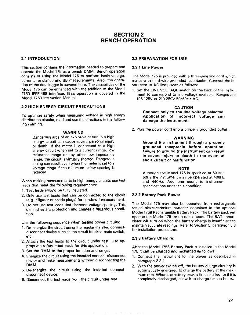
SECTION 2 BENCH OPERATION
2.1 INTRODUCTION
This section contains the information needed to prepare and operate the Model 175 as a bench DMM. Bench operation consists of using the Modal 175 to perform basic voltage, currant, resistance and dB measurements. Also, the opera- tion of the data logger is covered hare. The capabilities of the Model 175 can be enhanced with the addition of the Model 1753 IEEE-488 interface. IEEE operation is covered in the Modal 1753 Instruction Manual.
2.2 HIGH ENERGY CIRCUIT PRECAUTIONS
To optimize safety when measuring voltage in high energy distribution circuits, read and use the directions in the follow- ing warning.
WARNING Dangerous arcs of an explosive nature in a high energy circuit can cause sevare personal injury or death. If the mater is connected to a high energy circuit when set to a currant range, low resistance range or any other low impedance range, the circuit is virtually shorted. Dangerous arcing can result awn when the mater is sat to a voltage range if the minimum safety spacing is reduced.
When making measurements in high energy circuits use test leads that meat the following requirements: 1. Test leads should be fully insulated.
2. Only use test leads that can be connected to the circuit leg. alligator or spade plugs) for hands-off measurement.
3. Do not use test leads that decrease voltage spacing. This diminishes arc protection and creates a hazardous condi- tion.
Use the following sequence when testing power circuits: 1. De-energize the circuit using the regular installed connact-
disconnect device such as the circuit breaker, main switch, etc.
2. Attach the test leads to the circuit under test. Use ap- propriate safety rated leads for this application.
3. Sat the DMM to the proper function and range.
4. Energize the circuit using the installed connect-disconnect device and make measurements without disconnecting the DMM.
5. De-energize the circuit using the installed connect- disconnect device.
6. Disconnect the test leads from the circuit under test.
2.3 PREPARATION FOR USE
2.3.1 Line Power
The Model 175 is provided with a three-wire line cord which mates with third-wire grounded receptacles. Connect the ins strumant to AC line power as follows:
1. Sat the LINE VOLTAGE switch on the back of the instru- ment to correspond to line voltage available. Ranges are 105.12511 or 210.250V 50/60Hz AC.
CAUTION Connect only to the line voltage selected. Application of incorrect voltage can damage the instrument.
2. Plug the power cord into a properly grounded outlet.
WARNING Ground the instrument through a properly grounded receptacle before operation. Failure to ground the instrument can result in savere injury or death in the avent of short circuit or malfunction.
NOTE Although the Model 175 is specified at 50 and 60Hz the instrument may be operated at 400Hz and 440Hz. Add ona. count to instrument specifications under this condition.
2.3.2 Battev Pack Power
The Modal 175 may also be operated from rechargeable sealed nickel-cadmium batteries contained in the optional Model 1758 Rechargeable Batwry Pack. The battery pack will operate the Modal 175 for up to six hours The BAT annun- ciator will turn on when the battery charge is insufficient to maintain accurate readings. Refer to Section 5, paragraph 5.3 for installation procedures.
2.3.3 Battery Charging
After the Model 1758 Battery Pack is installed in the Model 175 it can be charged and recharged as follows: 1. Connect the instrument to line power as described in
paragraph 2.3.1. 2. With the power switch off, the battery charge circuitry is
automatically energized to charge the battery at the maxi- mum rata. When the battery pack is first installed, or if it is completely discharged, allow it to charge for ten hours.
2-1

NOTE For maximum battery efficiency only charge the battery pack after it has become discharged and only charge until it is fully charged (=,lOhours). Continuous charging over long periods of time will not damage the batteries but, usefu life will gradually decrease. This loss is not permanent and may be restored by cycling the battery pack through several complete charge/discharge cycles. The battery pack is capable of 500 to 1000 charge/discharge cycles before replace- ment is needed. Do not make measurements with the BAT an- nunciator on as the readings may be erroneous.
3. When the Model 175 is in use on line power, the battery charger maintains a trickle charge on the battery pack.
2.4 FRONT PANEL FAMILIARIZATION
The following paragraphs and Figure 2-l provide a brief description of the display, front panel controls and input ter- minals.
2.4.1 Display
The Model 175 has a 4 % digit liquid crystal display (LCD). The minus sign is displayed. The plus sign is implied by the absence of the minus sign. The following annunciators are displayed on the LCD. BAT-Low battery indicator for the Model 1758.
AC-AC selected (DC implied by absence of AC annun- ciator).
mV or V-Millivolts or volts selected. n, kR or Mn-Ohms, kilohms or megohms selected.
p, mA or A-Microamps, milliamps or amps selected. RMT (Remote)-Model 175 being controlled over the
IEEE-488 bus (Model 1753 installed).
C-Model 175 in calibration mode. AUTO-Autorange selected. REL--Relative selected.
dB-Decibel selected.
STO-Data being stored. RCL-Data being recalled. RCL flashes when buffer is full
during logging cycle.
2.4.2 Front Panel Controls
ON/OFF-Pressing in this pushbutton turns the Model 175 on. Releasing (out) this pushbutton turns the instrument off.
REL (Relative)-This pushbutton allows readings to be made with respect to any baseline value. Also allows zeroing of on range readings. See paragraph 2.7.2 for more detailed information on REL. dB-This pushbutton selects the dB function and is used along with the ACV or DCV function. Measurements are made in dBm referenced to 600% REL can be used to make any voltage level the OdB reference point for dB measurements. DATA LOGGER-Has min/max and 100 point reading storage capacity; records data at one of six selectable rates from every reading to 1 rdglhr. Records maximum and minimum conversion during the period the data logger is ac- tive at the rate of 3lsec.
1. STO/CLR-Pressing this button initiates the logging se- quence. Pressing the button a second time shuts off the data logger.
2. RCL-Pressing and holding this button in scrolls the data pointer. To read the data at a particular point, simply release the button.
AC/DC-This switch is used along with the volts (V), cur- rent (A), and dB functions. Depressing (in) this pushbutton selects AC and releasing (out) this pushbutton selects DC.
V-Depressing this pushbutton selects the volts function. O-Depressing this pushbutton selects the ohms function.
The AC/DC pushbutton must be released (out).
A-Depressing this pushbutton selects the current function. Range Push Buttons 1. AUTO-Depressing this pushbutton causes volts and
ohms to autorange. In current, it selects the 10A range (no autoranging in current).
%iEiq 175 AUTORANGING MVLTIMETER I
Figure 2-l. Model 175 Front Panel
2-2

2. Manual ranging is accomplished by depressing the ap propriate range button.
2.4.3 Input Terminals
The input terminals are intended to be used with safety shrouded test leads to help minimize the possibility of contact with live circuits. Safety shrouded test leads are supplied with the Model 175. VOLTS/OHMS/mA and COM (Red and Black)-Use this pair of terminals for all volt, ohm, milliamp and dB measurements.
10 AMPS and COM (White and Black)-Use this pair ex- clusively for measuring currant up to 10A (up to 20A for 15 seconds,.
2.4.4 Current Fuse Replacement
The current fuse protects the 200pA through 2000mA ranges from an input currant greater than 2A. To replace the current fuse, perform the following steps: 1. Turn off the power and disconnect the power line and test
leads. 2. Place the end of a flat-blade screwdriver into the slot in the
fuse holder on the front panel. Press in slightly and rotate the fuse carrier one-quarter turn counterclockwise. Release pressure and remove the fuse carrier and the fuse.
3. Remove the defective fuse and replace it with the follow- ing type: ?A, 250V. 3AG. normal-blow Keithley part number FU-13, or equivalent.
CAUTION Use only the recommended fuse type. If a fuse with a higher current rating is installed, instru- ment damage may occur.
2.5 ERROR MESSAGES
Table 2-l lists the error messages associated with basic front panel operation. Note that the instrument has a number of other massages that are discussed in the appropriate sections of this manual.
2.6 OPERATING CONDITIONS
2.6.1 Environmental Conditions
All measurements should be made at an ambient temperature within the range of OOC to 5OOC. and with a relative humidity of 0% to 80% up to 35OC. For instruments above 35OC derate humidity 3% per OC up to 50°C. If the instrument has been subjected to extremes of temperature, allow sufficient time for internal temperatures to reach environmental condi- tions. Typically, it takes one hour to stabilize a unit that is 10°C (18OF, out of specified temperature range.
Table 2-1. Error Messages
Comments
Model 175 locks up. See Section 5 for troubleshooting information.
Model 175 locks up, but operation can be restored by pressing any one of the four momentary pushbuttons. If restored, calibration is invalid as indicated by the flashing “C” annunciator. See Section 5 for troubleshooting information.
Overrange input applied to the Model 175. Leading minus sign indicates that input signal has a negative value.
“AC” and “R” annunciators flash. Correct problem by releasing (out, AC/DC pushbutton.
Table 2-2. Model 175 Maximum Allowable Inputs
Ranges -
200mV. 2V
20-1ooov 200mV
2.750V 200w-2000mA
10A All
Maximum Allowable Inputs
1OOOVDC or peak AC for less than 10s~ par minute. 300Vrms continuous. 1OOOVDC or peak AC. 750Vrms 1OOOV peak for lass than 1Osec per minute. 300Vrms continuous. lO’V*Hz maximum. 750Vrms. 1OOOV peak. 107V*Hz maximum. 2A, 250VDC or rms (fuse protected). 10A continuous; 20A for lbec (unfused,. 450VDC or peak AC
2-3

2.6.2 Maximum Allowable Inputs
Table 2-2 lists the maximum allowable inputs for the Model 175.
2.7 BASIC BENCH MEASUREMENTS
Basic measurement techniques for using the Model 175 to measure AC and DC volts, resistance, AC and DC current and dB are covered in the following paragraphs. Also in- cluded is the operation of the MIN/MAX and 100 point data logger.
WARNING Before operating the Model 175, observe the safety precautions found preceding Section 1. When testing high energy power circuits follow the procedure found in paragraph 2.2 High Energy Circuit Precau- tions. Failure to observe these and other safety precautions found in this manual could result in severe injury or death.
The COM terminal on the Model 175 is designed to float above earth ground to avoid ground loop problems.
WARNING Hazardous voltages may be applied to the COM terminal. The maximum allowable voltage between the COM terminal and chassis ground is 500V. Destruction of in- sulation, which could present a shock hazard, may occur if the 500V maximum is exceeded.
CAUTION Do not exceed the maximum input limits shown in Table 2-2.
2.7.1 Power-Up
NOTE The software revision level of the Model 175 can be displayed upon power-up by running the diagnostic program. See Section 5, Maintenance, for more information.
Turn on the Model 175 by pressing in the ON/OFF switch. The following will occur:
1. Reset-All zeros will be briefly displayed before going into the measurement mode.
2. RAM Test-If this test fails the Model 175 will lock up with zeros displayed.
3. NVRAM Test-If this test fails the display will show the error message “cErr”
Refer to Table 2-l for mc~re information pertaining to error messages.
2.7.2 Relative Mode
When the relative mode is selected with an on-scale reading on the display the following occurs: 1. The REL annunciator is displayed. 2. The next reading is stored.
3. The stored reading is then algebraically subtracted from all subsequent readings and displayed.
A REL level can be established for any measurement function (Volts, Ohms, Amps and dB1 and is effective only on that function. Changing functions will not affect a REL level already established. However, if another REL level is set (on any function) the previous REL level will be cancelled. For ex- ample, place the 175 in the R function and select the 2OOn range. Short the test leads and press the REL button. Note that the REL annunciator is on. Select DCV and note that the REL annunciator is off, indicating that there is not a REL level established for DCV. Switch back to 0 and note that the REL level is still there. Again, go to DCV and set a REL level of + IV. The REL annunicator will go on. Switch back to n and note that the REL annunciator is off, indicating that the REL level for 0 is cancelled.
Once a REL level is established for a measurement function, that stored level will be the same regardless of what range the Model 175 is on. For example, if + IV is established as the REL level on the 20VDC range, + IV will also be the REL level on the 1OOOVDC range.
It is important to note that the use of REL reduces the dynamic range of measurements by that level. For instance, assume that the REL level is +lV and the Model 175 is manually set to the 2V range. The maximum positive displayed reading, before overranging, would be +0.9999\1. This is because the A/D converter would be seeing 1.9999V (maximum) from the input. Thus, the dynamic range of measurement is -1.9999V to + 0.9999V (2.999BV) as com- pared to the normal -1.9999V to + 1.9999V (3.9998V). The dynamic range of measurement has been reduced by IV. The effects on dynamic range can be reduced by selecting a higher range or using autorange.
2.7.3 DC Voltage Measurements
The Model 175 can make DC voltage measurements between 1OhV and IOOOV. The basic procedure is as follows: I. Connect the test leads to the VOLTS and COM terminals
of the Model 175.
2. Select the DCV function. 3. Select a range consistent with the expected voltage. For
automatic range selection, press in the AUTO pushbutton.
NOTE Manual ranging is recommended for routine measurements above 200V.
2-4

4. Connect the test leads to the source as shown in Figure 2-2. If the positive source terminal is connected to the COM terminal of the instrument, the display will show a negative value. If the negative source terminal is con- nected to the COM terminal, the display will show a positive value.
5. Observe the display; if the “OL” message is shown, select a higher range until a normal reading is shown. Always use the lowest possible range for the best resolution.
6. Take the reading from the display.
NOTE High input impedance j VlOOOMRl DC volts measurements can be made on the 200mV and 2V ranges by releasing (out) all the function pushbunons (AC/DC, V, R, A).
DC VOLTAGE SOURCE
Figure 2-2. DC Voltage Measurements
2.7.4 TRMS AC Voltage Measurements
The Model 175 can make TRMS AC voltage measurements between IOwV and 75OV. Proceed as follows: 1. Connect the test leads to the VOLTS and COM terminals
of the Model 175. 2. Select the ACV function. 3. Select a range consistent with the expected voltage. For
automatic range selection, press in the AUTO pushbutton.
NOTE Manual ranging is recommended for routine measurements above 200V.
4. Connect the test leads to the source as shown in Figure 2.3.
5. Observe the display; if the “OL” message is shown, select a higher range until a normal reading is shown. Always use the lowest possible range for the best resolution.
6. Take the reading from the display.
NOTE See paragraph 2.8 for TRMS considerations.
AC VOLTAGE
Figure 2.3. TRMS AC Voltage Measurements
2.7.5 Resistance Measurements
The Model 175 can make resistance measurements between 1OmfI and 200MQ The 2MIf. 20MR and 200M12 ranges will autorange when the MI1 pushbutton is pressed in. Proceed as follows to make resistance measurements: 1. Connect the test leads to the OHMS and COM terminals of
the Model 175.
2. Select the II function.
NOTE The message “Err” and flashing II and AC an- nunciators will be displayed if the AC/DC push- button is pressed in. This is an invalid mode. To correct, simply release (out) the AC/DC pushy button.
3. Select a range consistent with the expected resistance. For automatic range selection. use the autorange mode.
NOTE Zeroing may be necessary to compensate for test lead resistance on the 20011 and 2kR ranqos. Zero the display as follows:
A. Short the to?., leads together. B, Press the REL pushbutton. The display will zero.
C. Proceed to step 4. 4. Connect the test leads to the resistance to be measured as
shown in Figure 2-4. 5. Observe the display: if the “OL” message reading is
shown, select a higher range until a normal reading is shown. Always use the lowest possible range for the best resolution.
6. Take the reading from the display
NOTE It is helpful to shield resistances greater than 106R (1MR) if a stable reading is expected. Place the resistance in a shielded enclosure and elect trically connect the shield to COM of the Model 175
2-5

Figure 2-4. Resistance Measurements
2.7.6 Current Measurements (DC or TRMS AC)
The Model 175 can make DC or TRMS AC current measurements between lO@A and IOA (20A for 15 seconds). If the expected current level is in question, make the initial measurement with the 10A range. This will help prevent the inadvertent blowing of the 2A current fuse.
NOTE For routine measurements above 10A it is recommended that the Model 1651, 50.Ampere current shunt be used.
1. For current measurements between 2000mA and 20A.
A. Connect the test loads to the 10 AMPS and COM ter- minals of the Model 175.
NOTE The test leads used must be capable of handling 20A and it is recommended that thev be twisted (see Figure 2-5) to minimize external iields which could affect the Model 175 or other equipment. Also, keep the test leads es short as possible to minimize voltage drop.
B. Select the ACA or DCA function.
C. Select the 10A range. Current does not autorange. D. Connect the test leads to the current source as shown
in Figure 2-5 and make the reading from the display. NOTE
Up to 5A may be applied continuously without degradation of the measurement due to self- hosting effects. Above 5A derate 0.15% rdg per amp for self-heating. For currents between IOA and 20A. specified accuracy can only be ob- tained when measurements are limited to a max- imum of 15 seconds.
2. For current measurements up to 2000mA:
A. Connect the test leads to the mA and COM terminals of the Model 175.
B. Select the ACA or DCA function. C. Select an appropriate range for the expected current.
Current measurements cannot autorange. D. Connect the test leads to the current source as shown
in Figure 2-6. If an overrange indication is displayed select a higher range until a normal reading is shown. Use the lowest possible range for the best accuracy.
E. Make the reading from the display.
CURRENT
TWISTED SOURCE
Figure 2-5. Current Measurements Between 2000mA and 20A
CURRENT SOURCE
Figure 2-6. Current Measurements up to 2000mA
2.7.7 AC Plus DC Measurements
Use the Model 175 to measure TRMS on a signal which has both AC and DC components as follows:
1. Measure and record the TRMS AC component as de- scribed in paragraph 2.7.4.
2. Measure and record the DC component as described in paragraph 2.7.3.
3. Compute the rms value from the following equation:
E -\/E RMS - DC 2 + E,,?
2.7.8 dB Measurements
The dB function makes it possible to compress a large range of readings into a much smaller scope. The relationship be- tween dB and voltage can be expressed by the following equation.
VW, dB = 20 log __ VFW
2-6
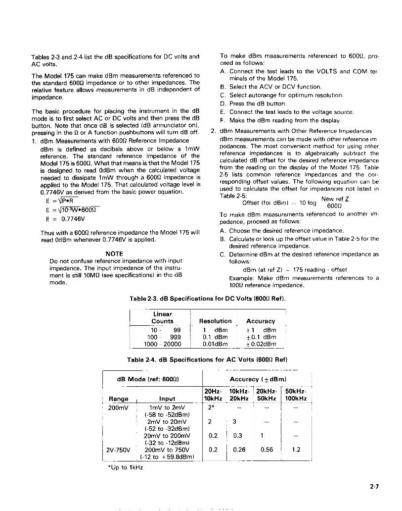
Tables 2-3 and 2-4 list the dB specifications for DC volts and To make dBm measurements referenced to 60012, pro- AC volts. ceed es follows:
A. Connect the test leads to the VOLTS and COM tern The Model 175 can make dBm measurements referenced to the standard 6OOn impedance or to other impedances. The relative feature allows measurements in dB independent of impedance.
minals of the Model 175. 8. Select the ACV or DCV function. C. Select autorange for optimum resolution.
D. Press the dB button. The basic procedure for placing the instrument in the dB mode is to first select AC or DC volts and then press the dB button. Note that once dB is selected (dB annunciator on), pressing in the 0 or A function pushbuttons will turn dB off.
1. dBm Measurements with 600R Reference Impedance dBm is defined as decibels above or below a 1mW reference. The standard reference impedance of the Model 175 is 600% What that means is that the Model 175 is designed to read OdBm when the calculated voltage needed to dissipate 1mW through a 600R impedance is applied to the Model 175. That calculated voltage level is 0.7746V as derived from the basic power equation.
E=\lP.R
E = IlO-3W.6000
E = 0.7746V
E. Connect the test leads to the voltage source.
F. Make the dBm reading from the display.
2. dBm Measurements with Other Reference Impedances dBm measurements can be made with other reference imp pedances. The most convenient method for using other reference impedances is to algebraically subtract the calculated dB offset for the desired reference impedance from the reading on the display of the Model 175. Table 2-5 lists common reference impedances and the cork responding offset values. The following equation can be used to calculate the offset for impedances not listed in Table 2-5:
New ref I Offset (foi dBml : 10 log -$,o;j
Thus with a 600R reference impedance the Model 175 will read OdBm whenever 0.7746V is applied.
NOTE Do not confuse reference impedance with input impedance. The input impedance of the instru- ment is still 1OMR (see specifications) in the dB mode.
To make dBm measutements referenced to another em- pedance, proceed as follows:
A. Choose the desired reference impedance. B. Calculate or look up the offset value in Table 2-5 for the
desired reference impedance.
C. Determine dBm at the desired reference impedance as follows:
dBm (at ref 2) = 175 reading offset Examole: Make dBm meawrements references to a lOOI deference impedance
Table 2-3. dB Specifications for DC Volts 16OOI1 Refl.
Table 2-4. dB Specifications for AC Volts l600R Refl
! dS Mode lref: 60001
Range / Input
200mV I 1mV to 2mV I i-58 to -52dBm)
~ (Ei, 2v.750v *Up to 1 ktiz
-
i?
Accuracy (* dSm)
OHz- 1 IkHz
2*
2
0.2
0.2 ~
i
IOkHz- / ZOkHz- 2OkHz 1 50kHz
- ! -
3
0.3 1
I
0.26 0.56
50kHz- 1OOkHz
-
-
1.2
2-7

i. lOOn is not listed in Table 2-5 so the offset must be 2.7.9 dB Measurement Considerations and Applica- calculated as follows: tions
offset = 10 log (j$$)
offset = -7.78dB ii. Subtract -7.78dB from all subsequent displayed
readings on the Model 175.
dBm measurements. referenced to another impedance, can be read directly from the display of the Model 175 by utilizing the REL feature, and an accurate voltage source. The basic procedure is as follows:
A. Calculate or look up the equivalent voltage level (Table 2-5) for OdBm at the desired reference impedance.
8. Input that voltage level to the Model 175. C. With the Model 175 in the dB mode, press the REL
button. D. dBm measurements referenced to the desired im-
pedance can now be read directly from the display of the Model 175.
3. dBW Measurements dBW is defined as decibels above or below a one watt reference. The procedure is the same as that found in paragraph 2.7.8 step 2. The only difference is that the reference point is OdBW (1W) rather than OdBm (1mW).
4. dElV Measurements dBV is defined as decibels above or below 1V (OdBV point). This is a voltage relationship independent of im- pedance. The basic procedure is to simply subtract 2.22 dl3 ITable 2-5) from all subsequent displayed readings on the Model 175..
5. Relative dB Measurements Just about any voltage level within the measurement limits of the Model 175 can be established as the OdB point. The basic procedure is to establish that level as the OdB point by using REL and make the desired dB measurements.
Table 2-5. Levels for Other Reference Impedances
Reference Equiv. Voltage Offset Impedance Level for: (600!7 Refl
(cl) OdBm OdBW OdBm OdBW 8 0.0894 2.828 -18.75 11.25
50 0.2236 -10.79 75 0.2739 9.03
150 0.3873 6.02 300 0.5477 3.01 600 0.7746 0.00
1000 1 .oooo 1 2.22
V, for OdBm = U10~3W-Z,,, V;z;;:: for OdBW =\6,,,
Offset (for dBm) = 10 log[6:& )
Offset (for ,,B,,,,) = ,O log
1. Typical Instrument Performance Typically, the Model 175 will perform better than its published dB specification. The following example will il- lustrate this point: A. Using the Model 175 in the dB mode 6000 ret)
measure a 1mV RMS. 1kHz source (common applica- tion in the communications field). Typically, the Model 175 will read -57.7dBm.
B. The calculated dBm level for that source is -57.8dBm.
C. The O.ldBm error is considerably better than the k2dBm specification. The specifications are intended to covet worst measurement conditions.
2. Measuring Circuit Gain/Loss Any point in a circuit can be established as the OdB point. Measurements in that circuit are then referenced to that point expressed in terms of gain I + dB) or loss (-dBl. To set the OdB point: A. Place the Model 175 in volts, autorange and dB. B. Connect the Model 175 to the desired location in the
circuit. C. Press the REL button. The display will read OdB. D. Gain/Loss measurements can now be made referenc-
ed to the OdB point. 3. Measuring Bandwidth
The Model 175 can be used to determine the bandwidth of an amplifier as follows: A. Connect a signal generator to the input of the
amplifier. B. Set the Model 175 to ACV and autorange. C. Connect the DMM and a frequency counter to the load
of the amplifier. D. Adjust the frequency of the signal generator until a
peak AC voltage reading is measured on the Model 175.
E. Press the dB button and then press the REL button. The OdB point is now established.
F. Increase the frequency input until the Model 175 reads -3.OOdB. The frequency measured on the frequency counter is the high end limit of the bandwidth.
G. Decrease the frequency input until the dB reading again falls to -3dB. The frequency measured on the signal generator is the low end limit of the bandwidth.
4. Determining Q The (1 of a tuned circuit can be determined as follows: A. Determine the center frequency and bandwidth as ex-
plained in paragraph 2.7.9 step 3. B. Calculate Q by using the following formula:
Q = Center Frequency/Bandwidth
2.7.10 MINIMAX and 100 Point Data Logger Operation
The data logger can store up to 100 readings and store the minimum and maximum readings recorded during the period that the data logger is active. The Data Logger remains active even after 100 points of data are stored, which means the MINIMAX readings continue to update. The only way to deactivate the Data Logger is to press the STOiCLR button (ST0 annunciator off1 or cycle power. The 100 points of data are stored at one of six selectable rates from three per second to one reading per hour. Readings for minimum and maxim mum are sampled at the rate of three per second regardless of the selected rate. The procedure for operating the data logger is as follows:
Connect the desired measurement configuration to the Model 175. Make sure that the controls of the Model 175 are set appropriately.
Loaainn Data: Press and hold the STOiCLR pushbutton. The follow- ing reading rates will scroll on the display:
r = 0 (every reading) r = 1 (1 rdglsecl I = 2 (1 rdgll0 set) r = 3 (1 rdglmin) r = 4 (1 rdg/lO min) r = 5 (1 rdgihr)
NOTE There is no need to select a rate if just minimum/maximum readings are desired. Momentarily press the STO/CLR button to start the logger. Release the STO/CLR pushbutton when the desired reading rata is displayed. The ST0 annunciator will turn on and data will be logged at the selected rate.
NOTE The logging cycle can be terminated at any time bv pressina the STOiCLR button. This shuts off tie’ data logger. However, data is retained and can be recalled at any time as long as the instru- ment remains on.
Data Retrieval Data can be retrieved at any time, but a flashing RCL an- nunciator indicates that the maximum number of readings (100) have been stored. A
6,
Press and hold in the RCL pushbutton. The display will scroll through the data points and MINIMAX (LO/HI). The first data point displayed will be the last stored reading. The next two data points will be the HI and LO readings made during that logging cycle. Notice that the longer the RCL pushbutton is held in the faster the data points will scroll on the display. Release the RCL pushbutton at the desired data point and note the reading (data) on the display. The data pointer can be incremented by steps of one by moman- tarily holding in the RCL pushbutton.
Shut off the data logger by pressing the STO/CLR pushbutton. All stored data will be retained until a new store cycle has commenced.
2.7.11 Diode Test
The 2kU and 200kfI ranges can be used for testing semicon- ductor junctions as follows: 1. Select 12 function.
2. Press 2k and 200k pushbuttons [diode symbols1 in simultaneously.
3. Display reads forward V drop of diode at 0.7mA lup to 2VI. Red terminal is positive.
2.8 TRMS CONSIDERATIONS
Most DMMs actually measure the average value of an input waveform but are calibrated to read its RMS equivalent. This poses no problems as long as the waveform being measured is a pure, low-distortion sine wave. For complex. none sinusodial waveforms, however. measurements made with an averagrng type meter can be grossly inaccurate. Because of its TRMS (True Root Mean Square1 measuring capabilities, the Model 175 provides accurate AC measurements for a wide variety of AC input waveforms
2.8.1 AC Voltage Offset
Typically the Model 175 will display 25 counts or less of offset on AC volts with the input shorted. This offset is caused by amplifier noise and offset of the TRMS converter. This offset will not affect reading accuracy and should not be zeroed out using the REL feature. The following equation expresses how this offset IV OFFsETJ is added to the signal input IV,,):
Displayed reading -\,&I2 ~+ iVoiFstri2 As long as V,, is at least 10 times larger than V,,,,,,, negligi~ ble error will occur.
Example: Range = WAC, range Offset = 25 counts input = 200mV RMS
Displayed Reading :: “!Q@!2 + (.Q025j2~ ~$:~~o’,,“,;“oooo”3
= .2OOOV RMS
If REL is used to zero the display. the 25 counts of offset would be subtracted from V,, resulting in an error of 25 counts in the displayed reading.
2.8.2 TRMS Measurement Comparison
The RMS value of a pure sine wave is equal to 0.707 times its peak value. The average value of such a waveform is 0.637 times the peak value. Thus. for an average-responding meter, a correction factor must be designed in. This correction fact tar, K, can be found by dividing the RMS value by the average value as follows:
K = 0.707 = 1.1, 0.637
2-9

By applying this correction factor to an averaged reading, a typi- cal meter can be designed to give the RMS equivalent. This works fine as long as the waveform is a pure sine. but the ratios between the RMS and average values of different waveforms is far from constant, and can vary considerably.
Table 2-6 shows a comparison of common types of waveforms. For reference, the first waveform is an ordinary sine wave with a peak amplitude of 1OV. The average value of the voltage is 6.37V, while its RMS value is 7.07V. If we apply the 1 .I 1 correc- tion factor to the average reading, it can be seen that both me- ters will give the same reading, resulting in no error in the aver- age-type meter reading.
The situation changes with the half-wave rectified sine wave. As before, the peak value of the waveform is 1 OV. but the average value drops to 3.18V. The RMS value of this waveform is 5.OOV, but an average responding meter will give a reading of 3.53V (3.18 x 1 .l l), creating an error of 29.4%.
A similar situation exists for the rectified square wave, which has an average value of 5V and a” RMS value of 5V. Here the average responding meter gives a reading of 5.55V (5 x 1 .i 1). while the Model 175 gives a TRMS reading of 5V. Other waveform comwrisons can be found in Table 2-6.
Table 2-6. Comparison of Average and TRMS Meter Readings
Wavefoml
Sine +10--
0 n
Half-Wave Rectified Sine
*b”n-
Full-Wave Rectified Sine
“,“m
SqlJX? +10- -
0 Fr
Rectified Square Wave 1ov 5.cw
1ov 1ov ‘v?j
1 1ov 5.77v
AVerage Responding
Meter Readine
7.07v
3.53v
7.07-9
ll.lOV
5.55v
ll.lV.ll
5.55v
2-10

2.8.3 Crest Factor
The crest factor of a waveform is the ratio of its peak value to its RMS value. Thus, the crest factor specifies the dynamic range of a TRMS instrument. For sinusodial waveforms, the crest factor is 1.414. For a symmetrical square wave, the crest factor is unity
The crest factor of other waveforms will. of course. depend on the waveform in question because the ratio of peak to RMS value will vary. For example, the crest factor of a rec-
50%
tang&r pulse is related to its duty cycle; as the duty cycle decreases, the crest factor increases. The Model 175 has a crest factor of 3. which means the instrument will give act curate TRMS measurements of rectangular waveforms with duty cycles as low as 10%
2.8.4 Extended Frequency Response
Figure 2-7 illustrates the extended frequency response of the AC volts ranges up to 1MHr.
1OHz 1OOHz 1kHz 1OkHz 1OOkHz ; 1MHz
0.1 FULLSCALE 2.750V RANGES
Figure 2-7. Model 175 Typical ACV Frequency Response
2.11/2-12


SECTION 3 PERFORMANCE VERIFICATION
3.1 INTRODUCTION 3.4 INITIAL CONDITIONS
This section contains information necessary to verify that the Model 175’s performance is within specified accuracy. Model 175 specifications may be found at the front of this manual. Ideally, performance verification should be performed when the instrument is first received to enwre that no damage or change in calibration has occurred during shipment. The verification procedure may also be performed whenever in- strument accuracy is suspect or following calibration. If per- formance on any of the ranges or functions is substandard. calibration can be performed as described in Section 5.
NOTE If the instrument does not meet specifications and it is still under warranty (less than 12 months since date of shipmentl, contact your Keithley representative or the factory to determine the action to be taken.
Before performing the verification procedures, make sure the Model 175 meets the following conditions:
1. If the instrument has been subject to temperatures below l@‘C 165°F) or above 2E°C 18Z°F1. allow sufficient time for the instrument to reach temperatures within the range. Generally, it takes one hour fo stabilize an instrument that is 10°C (18°F) outside of this range.
2. Turn on the Model 175 DMM and allow it to warm up for one hour. The instrument may be operated from either line power or battery pack power, as long as the battery pack has been fully charged as described in paragraph 2.3.3.
3.5 VERIFICATION PROCEDURE
The following paragraphs give the basic verification pro- cedure for the following functions: DC volts, AC volts, resistance, and current.
3.2 ENVIRONMENTAL CONDITIONS WARNING
All measurements should be made at an ambient temperature between 1W and 28X (65O to 82°F) with a relative humidity less than 80%.
3.3 RECOMMENDED TEST EQUIPMENT
The following procedures require that high voltages may be applied to the input ter- minals of the Model 175. Use normal precautions to avoid possible electrical shock which could result in personal injury or death.
Equipment for veri’fying the performance of the Model 175 is listed in Table 3-l. Alternate equipment may be used as long as the equipment accuracy is at least as good as the specifications listed in Table 3-l.
3.5.1 DC Voltage Accuracy Check
CAUTION Do not exceed 1OOOV between the VOLTSlOHMSlmA and COM terminals or damage to the instrument may occur.
Table 3-l. Equipment Specifications
Mfg Fluke
Fluke
Fluke
Resistance Calibrator
DC Current Calibrator
Specifications
200mV. 2v, zov, zoov, 1ooov ranges f 0.005% 200mV. 2V. 2OV. 1 OOV 50Hz to 10kHz. ?0.05% lOOR, lkll, 1OkR. lOOka ranges 1tO.00596; 1MR ranw ztO.Ol%: 1OMR range +0.05% 200rrA. 2mA. 20mA. 200mA. 2600mA ranges *0.025% 100mV. 1V. 1OV. 1OOV ranaes: 20Hz-‘50H; +ti.l% I 20kHz-100kHz *0.05% 1ooov range: lOHz-30Hz f0.12% 50kHz-100kHz -tO.lO%
3-l

1. Select the DC V function and 200mV range. 2. Connect the calibrator to the instrument.
3. Apply positive lOO.OOOmVDC to the Model 175. The reading must be within the limits specified in Table 3.2.
4. For each remaining range, apply the required voltage as specified in Table 3-2, and verify that the reading is within specifications.
5. Repeat all checks with negative voltage.
Table 3-2. Limits for dc Voltage Verification
dcV Applied Allowable Readings RaIIlX dc Voltaee (18” c to 280 C)
I I 200 mv 100.000 mV 99.94 to loo.06
2 v 1.lxQoo v 0.9995 to l.oco5 20 v lO.oiml v 9.995 to 10.005
200 v 100.000 v 99.95 to 100.05 loo0 v 1000.00 v 999.5 to 1000.5
3.52 AC Voltage Accuracy Check
CAUTION Do not exceed 750V RMS, IOOOV peak lOW*Hz, between the VOLTSlOHMSlmA and COM terminals or instrument damage may occur.
1. Select the AC V function and the 200mV range. 2. Connect the calibrator to the DMM. 3. Set the calibrator output to lOO.OOOmV AC at a frequency
of 2QHz. Verify that the reading is within the limits specified in Table 3-3.
4. Repeat the 1OOmV AC measurement at the other frequen- cies specified in Table 3-3.
5. Check the 2V. 2OV. ZOOV, and 750V ranges by applying the required voltages and frequencies specified in Table 3-3 end verifying that the readings are within the specified limits.
3.5.3 Resistance Accuracy Check
CAUTION Do not exceed 450VDC or peak AC be- tween the VOLTSlOHMSlmA and COM terminals or instrument damage may oc- cur.
1. Select the R function (AC/DC pushbutton must be out) and the ZOOQ range.
2. Connect the test leads to the Model 175 end short the other ends together.
3. Press the REL pushbutton to compensate for the test lead resistance.
4. Disconnect the short end connect the test leads to the calibrator.
5. Set the calibrator to lOO.OOOfl and verify that the reading is within the limits specified in Table 3-4.
6. Check the 2kR, 20kR, 200k0, and ML2 ranges by applying the required resistances specified in Table 3-4 end verifying that the readings are within the specified limits.
Table 3-4. Limits for Resistance Verification
c IWC to 28W
99.93 to 100.07 0.9994 to 1.0006 9.993 to 10.007 99.94 to 100.06
0.9993 to 1.0007
L
3.5.4 DC Current Accuracy Check
CAUTION Do not exceed 2A to the VOLTS/OHMS/ mA and COM terminals or the amp fuse will blow.
1. Select the DC A function end initially, the 2000mA range. 2. Connect the calibrator to the VOLTSiOHMSimA end
COM terminals of the Model 175. 3. Apply lOO.OOO~A end switch the Model 175 to the 200pA
range. The reading must be within the limits specified in Table 3-5.
4. Check the 2mA through 2000mA ranges by applying the required current specified in Table 3-5 and veribing that the readings are within the specified limits.
CAUTION Do not exceed 10A continuously or 20A for 15 seconds to the 10 AMPS and COM ter- minals or instrument damage may occur.
Table 3-3. Limits for ac Voltage Verification
XV Applied ac Allowable Readings (18°C to 28°C)
Range Voltage ZOH?.. ( SOHZ 1 1okkEz 1 2olrHz ! 5okHz 1MlkHz
200 mv loO.CCO mV 98.80 to101.20 99.30 to100.70 98.10 to 101.90 91.25 to 108.75 2 v 1.00000 v 0.9880 to1.0120 0.993U to1.0070 0.9860 to 1.0140 0.9675 to 1.0325 0.9300 to 1.07W
20 v 1o.m v 9.880 to10.120 9.930 to10.070 9.860 to 10.140 9.675 to 10.325 9.300 to 10.700 200 v 1oo.m v 98.80 to101.20 99.30 to100.70 98.60 to 101.40 96.75 to 103.25 93.w to 107.w 750 v 750.w v 740.5 to 759.5 744.2 to 755.8 -
52
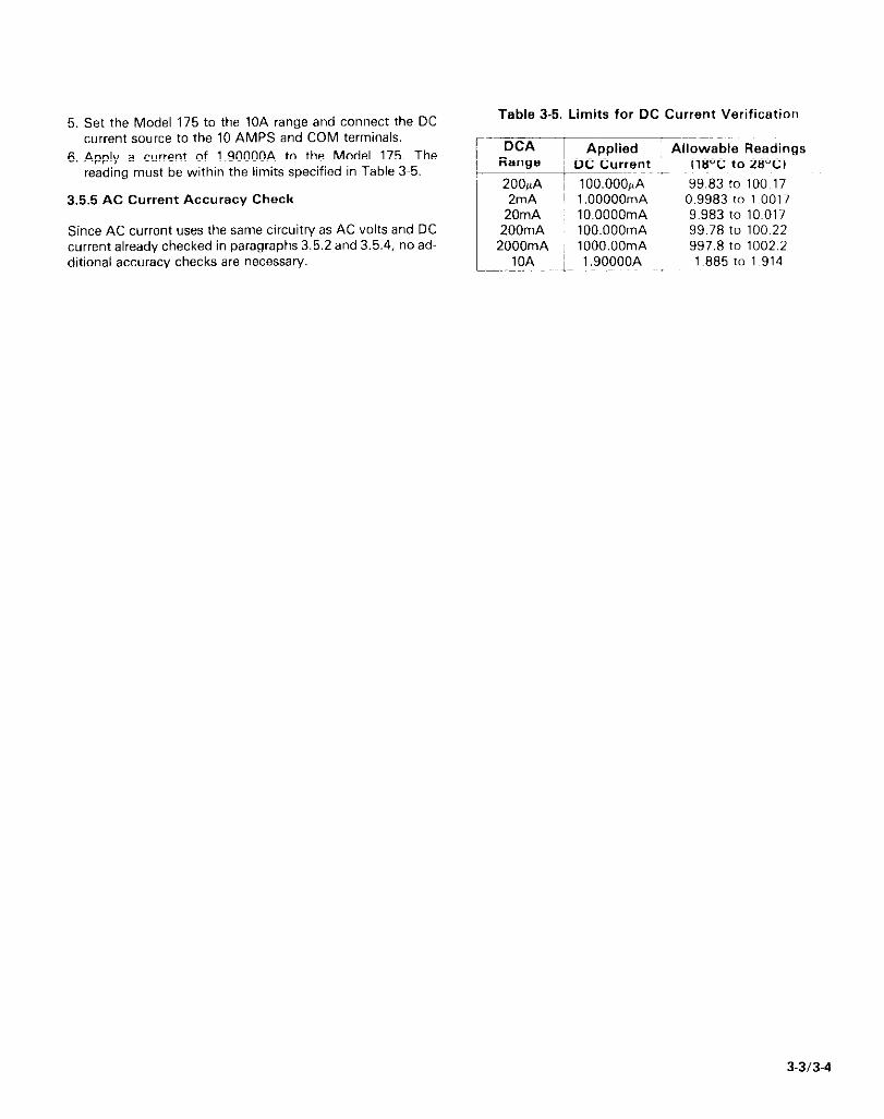
i for DC Current Verification Table 3-5. Limit!
i-Dt;#;tnt ““;,os,“‘;,,~;$d;gs
ZOOpA ~ lOO.OOOfiA 99.83 to 100.17 2mA 1 .OOOOOmA 0.9983 to 1~0017
5. Set the Model 175 to the 10A range and connect the DC current source to the 10 AMPS and COM terminals.
6. Apply a current of 1.90000A to the Model 175. The reading must be within the limits specified in Table 3-5.
3.5.5 AC Current Accuracv Check
Since AC current uses the same circuitry as AC volts and DC current already checked in paragraphs 3.52 and 3.5.4, no ad- ditional accuracy checks are necessary.
20mA : lO.OOOOmA 9.983 to 10.017 lOO.OOOmA 99.78 to 100.22
2000mA lOOO.OOmA 997.8 to 1002.2
J 1 .goF?oa 1.885 10 1.914
3-313-4

SECTION 4 THEORY OF OPERATION
4.1 INTRODUCTION
This section contains an overall functional description of the Model 175. Information pertaining to the Model 1758 Batten/ Pack option is also included. Detailed schematics and com- ponent layout drawings are located at the end of this instruc- tion manual.
4.2 OVERALL FUNCTIONAL DESCRIPTION
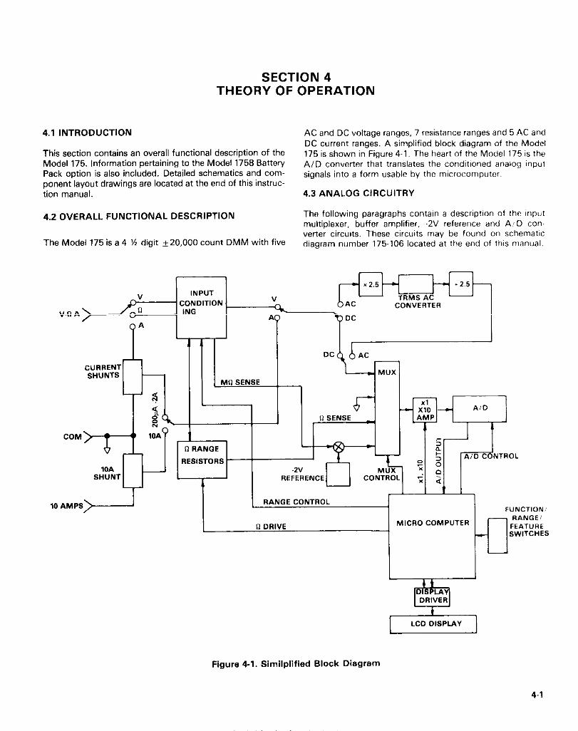
The Model 175 is a 4 % digit _+20,000 count DMM with five
AC and DC voltage ranges. 7 resistance ranges and 5 AC and DC current ranges. A simplified block diagram of the Model 175 is shown in Figure 4-l. The heart of the Model 175 is the AID converter that translates the conditioned analog input signals into a form usable by the microcomputer.
4.3 ANALOG CIRCUITRY
The following paragraphs conlair a description of the input multiplexer, buffer amplifier, -2V reference and AID cons wrier circuits. These circuits may be found on schematic diagram number 175-106 located at the end of this manual.
RESISTORS
10 AMPS RANGE CONTROL FUNCTION
n OFlIVE MlCRO COMPUTER
LCD DISPLAY
Figure 4-1. Similplifisd Block Diagram
4-1

4.3.1 Multiplexer
The multiplexer connects one of four signals to the buffer amplifier: Signal, zero, reference, ohms reference. The multiplexer, shown in Figure 4-2, is made up of 4 JFETS which are controlled by the microprocessor through U114. The FETs are driven by U109 and part of U106. The drivers convert the digital signals of the microprocessor to signals usable by the FETs.
a110
l
INPUT FROM MULTIPLEXER
CONVERTER
+ OUTPUT TO
OHMS a112 BUFFER Figure 4-3. Simplified Schematic of the Input Buffer
REFERNECE AMPLIFIER Amplifier
-4) 4.3.3 -2V Reference Source
The Model 175 voltage and current measurements are based on comparing the unknown signal with an internal -2V reference voltage. During each measurement cycle the
0113 microprocessor samples the unknown and uses it along with REFERENCE a zero measurement and -2V signal measurement to compute
the unknown voltage.
._. _ FROl
Figure 4-2. Simplified Schematic of the Multiplexer
Ordinarily; FET switching creates transients which could be seen in the final measurement. These effects are minimized in the Model 175 through the use of software generated delays and by shorting the multiplexer bus to signal common before each signal measurement through Cllll.
4.3.2 Input Buffer Amplifier
The input buffer amplifier provides the necessan/ isolation between the input signal and the AID converter. The amplifier is a noninverting, low noise, high impedance circuit with xl or x10 gain. The amplifier gain is controlled by the microprocessor and is range and function dependent. Figure 4-3 shows the simplified schematic of the input buffer amplifier.
The -2V reference is made up of a highly stable zener diode WRlOl). an op-amp and a resistive voltage divider. U103 and R120 A, B, C act as a constant current source to minimize the zener voltage variations. Fill7 C, D is then used to divide down the -6.35V zener voltage to -2V.
The output of U103 (-7V) is used as a reference voltage for the A/D converter and as a negative supply for various com- ponents.
4.3.4 AID Converter
The Model 175 uses a combination constant frequency charge balance, single slope analog-to-digital converter. A simplified schematic of the A/D used in the Model 175 is shown in Figure 4-4 with an associated output waveform.
4-2

” CHARGE BALANCE
RlZlA 1.w
0 INTEGRATOR
OUTPUT WAVEFCJRM
I I ‘CB
ELAY
I:-
A
INPUT ENABLE/DISABLE
PHASE PHASE
NEXT - MEASUREMENT PHASE Figure 4-4. AID Converter
4.3.5 input Signal Conditioning The charge balance phase begins when the input enable/disable line is set high. This occurs at the end of a software-generated delay period that allows the signal to set- tle after the appropriate multiplexer FET is turned on. The ac- tual delay period depends on the selected range and function.
For DCV and ACV the signal conditioning is performed by R106, its shunt capacitors, KlOl. K102. K103 b Q106.
SINGLE SLOPE
Once this occurs the signal from the buffer amplifier is added to the offset from RlZOH. This converts the bipolar signal from the buffer (* 2V) to an unipolar input to the integrator.
The integrator ramps up until it just passes the charge- balance comparator threshold voltage. When thejsing edge of Q3 occurs from U122 or when Ut 19 goes low. Q goes high forcing IcB into the integrator input. Since IcB is much greater than the current through R120G and R120H the in- tegrator output voltage will ramp in the negative direction. The integrator will continue ramping downward until U1198 goes low. Each time the output U121A goes high it is gated (inside the microprocessor) with the microprocessor’s inter- nal clock and these pulses are counted. Once U121A goes IOM, the process repeats itself.
The charge balance phase continues for 100msec. At the end of the charge balance phase, the output of the integrator is resting at sc~me positive voltage. Since the integrator output is connected to the noninverting input of the UlOBA, its out- put will stay high until the integrator ramps negative. During single slope Q114 is turned off and R121H is connected to +5V. The single slope comparator is then gated with the microprocessor’s internal clock and counted. Once the com- parator output goes low the microprocessor stops counting and can compute the reading.
The following attenuation is provided:
ln the DCV mode: + 1 is used on the 200mV Et 2V ranges. + 10 is used on the 20V range. + 100 is used on the 200V range. + 1000 is used on the 1OOOV range.
In the ACV mode: f 1 is used on the 200mV range. + 10 is used on the 2V range. i 100 is used on the 20V range. ~1000 is used on the 200V Et 1OOOV
range. Protection for the AC Et DC voltage ranges is provided by R103, R108, 0107 and 0108. RI03 and RlOE are used ex- clusively on the lower ranges of ACV Et DCV to limit current to 0107 and Q108 during overload. During the overload Q107 and QlO8 clamp the maximum voltage on the signal FET line to within 0.7V of the supplies.
Signal conditioning for current is performed by R109. RllO and I?119 current shunts. For DC current measurements the shunt voltage drop (200mV full scalel is applied directly to the input signal FET for conversion. In AC current, the shunt voltage drop is treated as a 200mV AC signal and is switched to the AC converter section. Overload clamping occurs at 3 diode voltage drops which is a level high enough to permit high crest factor current waveforms.
4-3

In DCV the properly scaled signal is applied directly to Ql IO through R107 and CllO. In the AC V mode the scaled analog signal is applied to the AC converter for transformation to a DC signal that is applied to QllO.
Resistance measurements are made using the ratiometric technique (see Figure 4-5). When the resistance function is selected a series circuit is formed between the ohms source, reference resistor and the external unknown resistance.
I RX = VZ.RREF “1
Ri06ARREF hM >TOQ113OF 1 OMR
T MULTIPLEXER RX
Figure 4.5. Resistance Measurements-Ratiometric Technique
Three reference resistors are used on the ohms ranges RlOl, R102 and R106A. RlOl is used for the 200R Et 2kR ranges, Figure 4-6. Simplified Schematics of Ohms Circuitry R102 for the 20kR and 200kcl ranges and R106A for 2MR. 20Mn & 200Mn. Drive for the ohms ranges is ultimately con- By measuring the four inputs to the AID converter the
trolled by the microprocessor through Ulll and U112. unknown resistance can be computed by the microprocessor using this equation:
Switching for the ohms ranges is done using low leakage base to collector diodes of 0102, 0104 and Q105. The ap- propriate transistor is turned on by driving the base high
Osense HI - &~nse LO RX =
nref HI--nref LO (+ 5V). The simplified schematics for the ohms circuitry is shown is Figure 4-6. For the 200% 20k0, 2Ml7 ranges fI sense HI is actually
multiplied by a factor of 10 in the buffer circuit: I3101 RRs~
-:‘
TO 0112 OF lkn FIT101 MULTIPLEXER Protection on the ohms ranges is accomplished by Q103,
4.15kn RTIOI, 0101, R103, Q107and Q108. Foran inputvoltageap-
RX plied to the R input terminals, QlOl clamps the voltage across
a1 04 RIO1 to a safe level. RTIOI limits current to Ql03 which clamps the voltage at 0104 to a safe limit (<12V).
For the 20k0 and 200kfl ranges protection is provided by R102, R104 and R105. Rl06A provides protection for the 2MiI. 20Mn and 200MR ranges by limiting current.
4.3.6 AC Converter
A. 2OOn and 2kn Ranges All AC voltage inputs pass through UIOI for a x2.5 voltage
4-4

amplification. The gain stage is used to permit accurate voltage measurement at higher frequencies and lower input lW&.
The output of UlOl is applied to the TRMS converter chip which converts the AC input signal to the corresponding DC level. The DC output is then -2.5 and applied to the signal FET.
4.4 DIGITAL CIRCUITRY
Model 175 operation is controlled by the internal microcorn- puter. This section briefly describes the operation of the Various Sections of the microcomputer and associated digital circuitry. A simplified block diagram is included for user reference; for more complete circuit details refer to schematic diagram number 175.106 at the end of this manual,
4.4.1 Microcomputer
The microcomputer centers around the 146805E2 CMOS microprocessor. It is an 8 bit microprocessor with direct ad- dressing of alp to 8k bytes on a shared address and data bus.
Timing of me microprocessor is accomplished by the use of Y101; a 3.2768MHz crystal. Internally this frequency is di- vided down by 5 to obtain a bus operating frequency of 655.36kHz. This is present on the address strobe of U123 (pin 6) and supplies timing to all other parts of the instrument through the binary divider U122.
The software for the MPU is stored in U115 (PROM). Tem- porary storage is provided by Ul13. U113 is used to share the calibration constants on power up and as RAM for the microprocessor’s in-house functions. It also stores readings for the data logger. UllO is the NVRAM and is used to store the calibration constants.
4.4.2 Address Decoding
U120 is used to latch in the address that is on the bus when the address strobe of U123 goes high and presents it to the PROM (U115) during data strobe.
4.4.3 PIA
U114 provides for most of the control of the instrument. It controls all ranging hardware, AID converter, and data out- put and input for the IEEE option.
4.4.4 Display Board
The LCD display is driven by a flat pack LCD controller chip U201 and it communicates to the microprocessor through 4 control lines. During power-up the microprocessor configures U201 to drive the triplexed display.
In order to drive the display correctly four voltages are obtained from R126. The clock required by U201 is obtained from U122.
The display board also houses the special function keys; d8, REL, STO/CLR and RCL.
4.5 DIGITAL CALIBRATION
The Model 175 uses digital calibration to eliminate all poten- tiometers in the instrument to facilitate calibration. The con- stants that the Model 175 uses are stored in a nonvolatile electrically alterable read only memory (UllOl, and are read on power-up of the instrument. There is one constant for each range on DCV, ACV and I?. On the DCA and ACA func- tions the 200mV DC and 200mV AC constants are used respectively.
4.6 POWER SUPPLY
Fuse F102 is the LINE FUSE which is internally accessible. SlOl is the power on/off switch and 5102 selects 115V or 230V operations by placing the transformer primary windings in parallel or series.
TlOl, the power rransformer has two secondary windings: one for the Model 175 and the other for the IEEE option (Model 1753). The bridge rectifier lCR104l functions as a fullwave rectifier for both the plus and minus supplies. R123 limits current 10 the 12V zener (VR1021 and to the batteries (if installed1 for charging. The zener acts as a pre-regulator to the + 5V regulator.
4.7 MODEL 1768 BATTERY OPTION
Maximum battery charging rate is achieved when the instru- ment is connected to line power and the on/off switch is off, Fullwave rectified voltage from CR104 is applied to R102 and BTlOl to charge the batteries. Cl101 acts as a current sink if the charging current rises above 150mA. The batteries are of the quick recharge type and will charge in 8 to 10 hours. With the instrument turned on the batteries will trickle charge at approximately 40mA.
With the batten/ pack installed, the negative supply is generated using a CMOS voltage inverter (UlOll. The output of the inverter is applied to CR101 and Cl01 for filtering.
Low battery detection is accomplished by fhe comparator IU102) and the microcprocessor. A voltage level of 8.8V across BTlOl signals the end of useful batten, life. The trip level for the comparator is set by R103 and R104.
4-514-0


SECTION 5 MAINTENANCE
5.1 INTRODUCTION
This section contains installation, service and calibration in- formation for the Model 175 and 1758 Battery Pack. In addi- tion to front panel calibration, a program for calibrating the Model 175 over the IEEE bus is included.
WARNING The procedures described in this section are for use only by qualified service person- nel. Do not perform these procedures unless qualified to do so. Many of the steps covered in this section may expose the in- dividual to potentially lethal voltages that could result in personal injury or death if normal safety precautions ere not ob- served.
5.2 TOP COVER REMOVAL/INSTALLATION
The top cover of the Model 175 must be removed in order to service the unit or to install the Model 1758 battery pack and/or the Model 1753 IEEE-488 interface. Proceed es follows:
WARNING Disconnect the line cord and 811 other sources and cables before removing the top cover.
1. Turn off the power, disconnect the line cord and remove all teet leads from the terminals of the Model 175.
2. Turn the unit over and remove the four screws from the bottom of the case.
3. Turn the unit over again and separate the top cover from the rest of the unit.
4. To reinstall the top cover, position the tilt bail properly into the bottom cover and reverse the above procedure.
5.3 BAlTERY PACK (Model 1758) INSTALLATION
Refer to Figure 6-l and perform the following procedure to in- stall the battery pack:
WARNlNG Installation of the battery peck should only be performed by qualified personnel. Disconnect line cord and remove all test leads from the terminals of the Model 175.
1. Remove the top cover as explained in paragraph 5.2.
2. Remove the shield by pulling up on either side until the back lip disengages from the retaining clip. Ease the shield out of the unit.
Position the battery board as shown in Figure 6~1 and secure it to the shield using two supplied screws. The screws are fed through the shield into the battery board fasteners. Place the battery pack in the bracket and position if on lhe shield as shown. Feed the two screws through the shield into the bracket and tighten.
CAUTlON Do not allow the battery leads to short together or damage to the batteries may occur.
5. Carefully place the shield iwith battery pack1 back into the Model 175 so that it seats properly on the two spacers. Press down firmly on the back of the shield to engage it ins to the retaining (and ground1 clip.
6. Connect the ribbon cable from the battery board to the male connector (marked BATTERY) on the mother board.
CAUTION Make a close visual inspection to ensure that the connectore are properly mated or damage to the instrument may result.
7. Connect the red battery lead to the + RED terminal pin on the battery board. Connect the black batten, lead to the -ELK terminal pin on the batten, board.
8. Reinstall the top cover as explained in paragraph 5.2. 9. Charge the batten/ pack per instructions in paragraph
2.3.3.
5.4 TROUBLESHOOTING
The troubleshooting instructions contained in this section are intended for qualified personnel having a basic understanding of analog and digital circuitry. The individual should also be experienced et using test equipment es well es ordinary troubleshooting procedures. The information presented here has been wrinen to assist in isolating a defective circuit or circuit section; isolation of the specific componenf is left to the technician.
NOTE Avoid touching the PC Board or its component parts. Handle the PC Board by its edges.
5.4.1 Recommended Test Equipment
The success or failure in troubleshooting the Model 175 depends not only on the skill of the technician, but also relies heavily on accurate, reliable test equipment. Table 5-1 lists the minimum equipment and specifications recommended for troubleshooting the Model 175. Other equipment such as logic analyzers, capacitance meters, etc, could also be helpful in difficult situations.
5-l

Dual-trace. triqqered-sweeD oscillo- 1 scope, Dd to%MHz bandwidth.
5.42 Self Diagnostic Program
To use the self diagnostic program, hold in the dB button and turn on the Model 175. The following will occur: 1. All LCD digits and annunciators will turn on. 2. The software revision level will be displayed (i.e. All. 3. The sequential display test will run. 4. The Model 175 will go into the troubleshooting test mode.
If the dB button is released the instrument will flag either RAM or NVRAM self test failures, should they occur. If neither RAM nor NVRAM fails, the instrument will default to the troubleshooting test mode.
RAM Test--If the RAM test fails, the Model 175 will lock up with all zeroes displayed. Replacing U113 may correct problem. Non-Volatile RAM Test-If the NVRAM test fails the follow- ing message will be displayed:
GE I- r_j -
This is a sufficient message indicating that the instrument is probably not properly calibrated since calibration constants are stored in the non-volatile RAM. The Model 175 will lock up at this point if the test fails, but operation may be restored for troubleshooting by pressing any front panel control but- ton. The flashing “C” annunciator will indicate that the unit failed the NVRAM test.
At this point try calibrating the instrument with the constants already entered by simultaneously pressing in REL and dB un- til CAL is displayed, and then again until Stor is displayed. If the error gets corrected, indicating that the NVRAM is prob- ably good, a full calibration will be needed. If the error per- sists try replacing the NVRAM chip (UllO). Again, the Model 175 must undergo a complete calibration after the problem is corrected.
Sequential Display Test-Segments and annunciators are sequentially displayed in eight steps. Use Figure 5-1 for seg- ment identification. The steps are as follows:
f I I
b
d
Figure 5-l. Segment Identification
1. The “a” segments of the digits, and the dB and V annun- ciators are displayed.
2. The “‘b” segments of the digits are displayed. 3. The “c” segments of the digits are displayed. 4. The “d” segments of the digits, and the m (mAI RCL and
RMT annunciators are displayed. 5. The “e” segments of the digits, minus sign and the REL.
M and R annunciators are displayed. 6. The “f” segments of the digits, and the AUTO, BAT, m
(mV) and c annunciators are displayed. 7. The “g” segments of the digits, and the AC and k annun-
ciators are displayed. 8. The decimal points, most significant digit and the STO, F
and A annunciators are displayed.
Troubleshooting Test Modes-The troubleshooting mode is designed to switch on various switching FETs, transistors and logic levels to allow signal tracing through the instru- ment. The first displayed mode will reflect the selected func- tion and range. For example, assume that “0~1” is displayed. The ‘Ii corresponds to the volts function, the “1” cor- responds to the 200mV range and the “0” is the test number. The test number can be changed by pressing in the dB button. Table 5-2 lists the test modes for all functions and ranges.
To update the test mode, select the new function and range and hold in the dB button until the function symbol changes.
Troubleshooting consists of selecting the desired test mode and using the data found in Table 5-2 to signal trace the cir- wit.
5-2

NOTES: 2. Do not use AUTO when in AC or DC volts. 1. When a different function or range is selected the d6 but- 3. Use AUTO when checking circuitry on the 20MI1 and
ton must be pressed and held in to update the display with 200MR ranges (X&l. the corresponding test mode
Table 5-2. Troubleshooting Modes
Function Et Flange
200MVDC
2VDC
20VDC
200VDC
1OOOVDC
200mVAC
2VAC
20VAC
200VAC
750VAC
ACAbDCA ALL Ranges
1 t t
Test Mode
Oul lul 2ul 3ul
ou2 lu2 2u2 3~2
ou3 lu3 2~3 3u3
ou4 - lu4 2~14 3u4
ou5 lu5 2~15 3u5
Oul lul 2ul 3ul
ou2 lu2 2u2 3~2
ou3 lu3 2~3 3u3
ou4 lu4 2~14 3u4
ou5 lu5 2~5 3u5
OAl-OA6 lAl-lA6 2A-2A6 3Al-3A6
AMP Gain IU105*I
x10 x10 Xl Xl
Xl Xl Xl Xl
Xl Xl Xl Xl
Xl Xl Xl Xl
Xl Xl Xl Xl
x10 x10 Xl Xl
x10 x10 Xl Xl
x10 x10 Xl Xl
x10 x10 Xl Xl
x10 x10 Xl Xl
x10 x10 Xl Xl
Multiplexer FET On
QllO Qlll Q113 Qlll
(1110 Qlll Q113 Qlll
QllO a111 Q113 Qlll
QllO Qlll Q113 Qlll
QllO Qlll (1113 Qlll
QllO Qlll Q113 Qlll
QllO Qlll (1113 Qlll
QllO Qlll Q113 Qlll
~0110 Qlll Q113 a111
QllO Qlll Q113 Qlll
QllO Qlll Q113 Qlll
I Ohms ; Range Control
Logic levels on U114
; 1 0 1 0 1 0 1 0
1 0 1 0 1 0 1 0
0 0 0 0 0 0 0; 0
01 0 0’ 0 0 0 01 0
0'1 0; 1 0:l 0 1 -~~~~ +-- 1 1 1 1 1 1
1: 1 1; 1
0: 1 0: 1 0: 1 0 1
5-3

Function Et Range
200R
2kR
20kIl
200kfl
2MII lML2)
20 b 200M0 (Auto)
Test Mode
001 101 201 301 401 501 601
002 102 202 302 402 502 602
003 103 203 303 403 503 603
004 104 204 304 404 504 604
005 105 205 305 405 505 605
006 106 206 306 406 506 606
Table 5-2. Troubleshooting Mode (Cont.)
Amp Gain
(U105’
x10 x10 Xl Xl
Xl Xl
Xl Xl Xl Xl
Xl Xl
x10 x10 Xl Xl
Xl Xl
Xl Xl Xl Xl
Xl Xl
x10 x10 Xl Xl
Xl Xl
Xl Xl Xl
Xl Xl
1 ’ i
Multiplexer FET On
0110 Qlll Q112 QllO
Qlll Q113
QllO Qlll Q112 (3110
Qlll Q113
QllO Qlll Q112 QllO
Qlll 0113
QllO 0111 Q112 QllO
Qlll 0113
0110 Qlll Q113 QllO
-
Qlll Q113
a1 10 0111 Q113
Ohms Range
rransistors On
Q104~ Q104 Q104 (1104
-
-
Q104 Q104
Q104 Q104 Q104 Q104
Q104 Q104
Q105 Q105 Q105 Q105
Q105 Q105
Q105 Q105 Q105 Q105
Q105 Q105
Q102 Q102 0102 Q102
- Q102 Q102
Q102 0102 Q102
Qlll 0102 Q113 Q102
Range ControlI igic levels on U114 LO
PA0 PA
1 1 1 1 1 1 1 1
1 1
1 1 1 1
1 1
0 0 0 0
0 0
0 0 0 0
0 0
1 1 1 1
1 1
1 1
1 1
1 1
1 1 1 1
1 1
1 1 1 1
1 1
1 1 1 1
1 1
1 1 1 1
1 1
1 1 1
1 1
PA2
1 1 1 1
1 1
1 1 1 1
1 1
1 1 1 1
1 1
1 1 1 1
1 1
0 0 0 0
0 0
E 0
0 0
1 1
gain. * f4 to 5V (Logic 1) at pin 9 of U106El selects X10 gain, OV (Logic 0) at pin 9 of U106B selects the Xl 5.4.3 Power Supply and Battery Pack (Model 1758)
Checks perly before attempting to troubleshoor the signal condition-
PA3
0 0 0 0
Table 5-3 shows the various checks that can be made to the ing circuits. Check these circuits using the information in
power supplies within the Models 175 and 1758. In addition Tables 5-4 and 5-5.
to the normal voltage checks, it is a good idea to check the various supplies with an oscilloscope to make sure no noise
5.4.5 Signal Conditioning
or ringing is present. These circuits can be checked by using the diagnostic pro- 5.4.4 A/D Converter and Display gram (troubleshooting modes). See paragraph 5.4.2. Make sure the A/D converter and display are operating pro-
5-4

Table 5-3. Power Supply Checks end Battery Pack (Model 17581 Checks
Step Item/Component
1 5102 Line Switch 2 F102 Line Fuse 3 Line Cord
4 U116”* Input Win)
t
5 u1w* Output IV0 6 U117 Input Win) 7 u117 Output Wo’ 8 VRlOl 9 U103 pin 6
10” QlOl base
11’
12” UlOl pin 8 13” U102 pin 7
*Checks for the Model 1758
Required Condition
Set to 115 on 230V as required Continuity. Plugged into line receptacle; power on +12v *lo% +5v *5% -20v to -14v -lov *lo% -6.25V to -6.45V -7v *5% 0.6V while charging (power switch off) Line cord disconnected, battery pack charged, power switch on. >E.EV + 5V with batteries charged
Remarks
S102 externally accessible from rear panel.
+ 5V regulator input. + 5v regulator output. Negative supply input. Negative supply output. Reference zener diode. Low noise negative supply. Current sink.
Voltage inverter. Voltage comparator.
**If U116 is replaced, be sure that the device is properly seated on the mother board so that it will not touch the IEEE board (if installed’.
Table 5.4. A/D Converter Checks
step
1
Item/Component
2 U123, pin 38 3 U122, pin 10 4 U122, pin 6 5 U122, pin 5 6 U122, pin 7 7 U122, pin 12
8 U119B. pin 6
9 U104, pin 6 10 U108, pin 6 11 UlOEB, pin 7
12 U121A, pin 6
13 U107A. pin 15
14 U107A. pin 10
15 U121B. pin 9
Required Condition
Turn on power; select 2V DC range. Short input. 3.2768MHz Clock 655.36kHz Clock 81.92kHz Clock 40. 96kHz Clock 163.84kHz Clock 1.28kHz Clock
+5V to =OV pulse train, 3pec duration every 22~~ Integrator Ramp = 1.5v Variable pulse train OV to +5v. Variable pulse train, OV to +5v. Variable pulse train, OV to +5v. I 5msec positive going pUlSEIS. 1OOmsec positive going pulse.
Remarks
Crystal (YlOl’ Address strobe Synchronous clock for A/D Synchronous clock for A/D Synchronous clock for AID Integrator timebase and real time interrupt. Charge balance synchronization signal.
Comparator Reference Comparator Output
Reference current generator.
Control line for charge balance/single slooe. Control line for integrator
5-5

Table 5-5. Display Board Checks
r-m-~- step
‘i ! 2
3 4 5 6 7 8 9
Item/Component
P1006. pin 5 P1006, pin 6 P1006. pin 7 P1006. pin 2 P1006. pin 1 P1006, pin 12 P1006. pin 13 P1006. pin 14
10 LCD 11 Connector (P1006)
5.5 LINE FUSE REPLACEMENT
Required Conditions
Turn on power: select the ZVDC range. + 3.33v + 1.66V +5v i5% 81.92kHz ov to + 5v Pulses ov to + 5v Pulses ov to + 5v Pulses + 5v to ov Pulses Check that LCD is positioned properly. Check that connector is not reversed. If reversed, display test will run, then display will blank. Check that they are positioned properly.
The line fuse is located internally in the Model 175. For exact fuse location, refer to Figure 6.1. To replace the fuse proceed as follows:
WARNING Disconnect the line cord and all other sources before removing the top cover.
1. Remove the top cover as explained in paragraph 5.2.
2. If the Model 1753 IEEE-488 interface is installed it must be removed to gain access to the fuse. The IEEE board is secured to the mother board by a support post at the rear. and a connector on the left side. To remove. lift board up until it disenages from the connector and support post.
3. Replace the blown fuse with the following type: 1BA. 25OV. 3AG. Sk-Blc IKeithley P/N-F&20).
CAUTION Do not use a fuse with a rating higher than specified or instrument damage may occur. If the instrument persistently blows fuses, a problem may exist within the instrument. If so. the problem must be rectified before continuing operation.
4. If the IEEE interface was installed, reinstall by reversing the procedure in step 2.
5. Reinstall the top cover as explained in paragraph 5.2.
5.6 SPECIAL HANDLING OF STATIC SENSITIVE DEVICES
CMOS devices are designed to operate at very high im- pedance levels for low power consumption. As a result, any normal static charge that builds up on your person or clothing may be sufficient to destroy these devices if they are not handled properly. Table 5-6 lists the static sensitive devices in
Remarks
Vlcdl Vlcd2 Power to display clock. Data From up Data From up Data From lp Data From pp
the Model 175. when handling these devices, use the follow- ing precautions to avoid damaging them.
1. The ICs listed in Table 5-6 should be transported and handled only in containers specially designed to prevent static build-up. Typically. these parts will be received in static-protected containers until ready for installation.
2. Remove the devices from their protective containers only at a properly grounded work station. Also ground yourself with a suitable wriststrap.
3. Handle the devices only by the body; do not touch the pins.
4. Any printed circuit board into which the device is to be in- serted must also be grounded to the bench or table.
5. Use only antistatic type solder suckers. 6. Use only grounded soldering irons.
Table 5-6. Static Sensitive Devices
5-6

5.7 FRONT PANEL CALIBRATION
Calibration should be performed every 12 months, or if the per- formance verification procedures in Section 3 show that the Model 175 is out of specification. If any of the calibration proce- dures in this section cannot be performed properly, refer to the troubleshooting information in this section. If the problem per- sists, contact your Keithley representative or the factory for fur- ther information.
The entire calibration procedure may be performed without hav- ing to make any internal adjustments if frequency compsnsa- tiw (see paragraph 5.7.6) has been verified. It is suggested that the 2V. ZOV, and ZOOV ranges at 1OkHz be checked (Section 3 Performance Verification) before proceeding.
TheModel 175 Multimeter has been improved to make calibra- tion of the instrument more convenient for the user. Later war- sions of the Model 175 (with Revision B or C software) can now be calibrated without having to open up the unit.
To determine what level your instrument has, hold in tha dB but- ton and turn on the Model 175. First, all LCD digits and annun- ciators turn on, then the software revision level will be displayed (for example, Al). The instrument will then run a display test and go into troubleshooting diagnostics. Cycle power to return unit to normal operation.
5.7.1 Recommended Calibration Equipment
Calibration can be performed using the Fluke Model 51018 Calibrator. Alternate test equipment may be used as long as the equipmenfs accuracy is at least as good as the specifications listed in Table 5-7.
Table 5-7. Recommended Callbratlon Equipment
Description
DC Voltage Calibrator
AC Voltage Calibrator
Resistance Calibrator
Specifications
200mV, ZV, 2OV, 2OOV, 1 ioov ranges 10.005% accuracy. 200mV. 2V. 2OV, 2OOV. 11 oov ranges M.05% ac- C”,TXY. lOOR, IkR. lOkR, 1ookR ranaes M.005%. 1 Mii range so.01 % IOMn range ~1~0.05%
Fluke 51018
Fluke 51018
Fluke 51018
5.72 Calibration Enable
If you have Revision A level software in your Model 175, then there is an internal calibration jumper that enables permanent storage of calibration constants.
The Model 175 is shipped with its internal calibrationjumperin a disabling position. In this position, calibration cannot be done. The jumper must be placed in its enabling position to allow cali- bration. Proceed as follows:
WARNING Disconnect the line cord and test leads from the terminals of the Model 175 before removing the top cover.
1. Remove the top cover as explained in paragraph 5.2. 2. The calibration jumper is located in the middle of the
mother board right behind the shield. Move the calibration jumper from position A to position B as shown in Figure 5-2.
3. Replace the top cover; plug the line cord back in and turn the instrument on.
Revision El Software
If you have Revision B level software in your Model 175, then you no longer have to remove the top cover to calibrate the in- strument if frequency compensation has been verified. The ins strument may be calibrated from front panel buttons.
The Model 175 must be in calibration storage enable in order to realize permanent storage of the calibration constants. If the 1”~ strument is not placed in enable. subsequent calibration will be lost when the instrument is turned oft. Perform the following steps to place the Model 175 in calibration storage enable:
1. If the Model 175 is presently on, turn it off using the ON. OFF power switch.
2. While holding in ths STOiCLR button, turn the instrument on using the ON/OFF power switch.
3. When the message ‘CAY is displayed, release the STO; CLR button. ‘CAL” will disappear. the instrument will return to the normal mode, and storage of calibration constants IS enabled.
4. Press in the REL and dB pushbuttons simultaneously until the message ‘CAL” is displayed again. Release the bull tons. The unit is now ready to be calibrated as indicated by the ‘c” annunciator an the display.
Revision C Software
Lastly, if you have Revision C level sofhvare in your Model 175. a rear panel external switch has been added to your instrument. When this switch is in ENABLED, it allows you to permanently store calibration constants.
The Model 175 is shipped from the factory with its external CALIBRATION switch in the DISABLED position. In this pow tion. calibration constants cannot be stored when entered from the front panel or over ths IEEE-486 bus. The switch must be moved to ENABLED to allow calibration constant storage.
The CALIBRATION switch is located in the middle of the rear panel. Slide the switch to ENABLED. Plug in the line cord and turn on the instrument. Press in the REL and dB pushbuttons simultaneously until the message ‘CAL” is displayed Release the buttons. The unit is now in calibration as indicated by the ‘C” annunciator.
5.7.3 Environmental Condltlons
Calibration should be performed under laboratory conditions having an ambient temperature of 23 k3”C and a relative hu- midity of less than 70% With the instrument on, allow it to warm up for one hour. If the instrument has been subjected to tem-
5-7
peratures outside this range, or to higher humidity, allow at least one additional hour for the instrument to stabilize before begin- ning the calibration procedure.
WARMNG Some procedures require the use of high volt- age. Take care to prevent contact with live cir- cuits which could cause electrical shock result- ing in injury or death.
NOTE Calibration can be stopped at any time and only se- lected ranges can be calibrated if needed.
5.7.4 DC Voltage Calibration ‘dB annunciator must be on (indicated two-point calibration).
Connect the calibration source to the VOLTS and COM termi- nals of the Model 175.
5.7.6 Resistance Calibration
1. Press in the REL and dB pushbuttons simultaneously until the message ‘CAL” is displayed. Replace the buttons. The unit is now in the calibration mode as indicated by the “G” annunciator.
2. Set the voltage calibrator to output OV. 3. Press the REL button (REL on). 4. Set the Calibrator Voltage output according to the range as
shown in Table 5.6. 5. Adjust the display of the 175 to read the same a?. the volt-
age of the calibrator with the use of the STO/CLR and RCL buttons. The STOKLR button increments the displayed reading and the RCL button decrements the displayed reading.
With the Model 175 still in the calibration mode (“C annunciator on), select the n function and connect the test leads to the OHMS and COM terminals of the Model 175. Table 5-10 sum- marizes the procedure.
1. With the test leads connected to the Model 175, short the other ends together.
2. Select the 200R range and press the REL button on the Model 175. The REL annunciator will turn on and the dis- play will zero (test lead compensation).
3. Disconnect the short and connect the test leads to thecali- brator.
6. Select the next range. 7. Repeat steps 2 through 6 for the remaining DC voltage
ranges in Table 5-6.
Table 5-8. DC Voltage Calibration
4. Set the calibrator to output lOOn and adjust the display, using the STO/CLR and RCL buttons for a reading of 100.00f~.
5. Press the REL button and note that the REL annunciator turns off.
6. Select the 2kR range and again short the test leads to- gether.
7. Press the REL button. The REL annunciator will turn on and the display will zero. 175
Range
200MV
Calibrator 175 Voltage Reading
190.000mV 190.00mV
1 1000v 1 1ooo.oov 1 1ooo.ov 1
5.7.5 AC Voltage Calibration
With the Model 175 still in the calibration mode (‘C annunciator on), select the AC volts function and connect the calibration source to the VOLTS and COM terminals of the Model 175. Steps 1 through 6 must be performed in the exact sequence listed.
1. Select the 200mV range and set the calibrator to output 190.000mV @ 200Hz.
2. Adjust the display using the STO/CLR and RCL buttons to read 190.00mV AC.
3. Press the d6 button and verify that the dB annunciator is on.
4. Set the calibrator to output 19.0000mV @ 200Hz. 5. Adjust the display to read 19.00mV. 6. Press the REL button and verify that the dB annunciator is
off
7. Repeat only steps 1 and 2 for the remaining ranges using Table 5-9 as a guide.
Table 5-9. AC Voltage Calibration
175 Range
200mV
Calibrator Calibrator 175 Voltage Frequency Reading
190.000mV 200Hz 190.00mV
6. Reconnect the test leads. set the calibrator to output IkQ and adjust the Model 175 for a reading of 1 .OOOOkR.
9. Press the REL button to turn off REL. 10. Select the 20k range and set thwxfibrator tc Jatput 1 OWL.
Adjust the Model 175 to read 1 O.OOOka. 11. Repeat step 6 for the 2OOW1,2Mnand 20MR ranges using
Table 5-l 0 as a guide.
Table 5-10. Resistance Calibration
175 Calibration 175 Range REL’ Resistance Reading
200R on 1000 1 oo.oon 2ka on lks1 1.00001&l
2OkR off I oka 1 o.oookR 2ookQ off lOOka 1 oo.oowz
2MR off 1MR 1 .OOOOMn 20Mn off 1 OMn 1 O.OOOMR
*REL is used to compensate for test lead resistance an the 200R and 2m ranges.
5.7.7 Frequency Compensation
Check high frequency (10kHz) AC volts accuracy as explained in section 3, Performance Verification. In the event that fre-
5-a
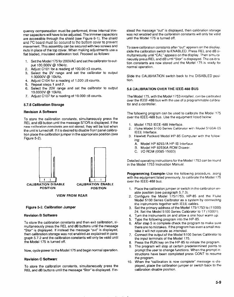
quency compensation must be performed. three internal trim- mer capacitors will have to be adjusted. The trimmer capacitors are accessible through the shield (see Figure 6-l). The shield and PC board must be secured to the bottom cover to prevent movement. This assembly can be secured with two screws and nuts in place of the top cover. When making adjustments use a flat bladed, insulated calibration tool. Proceed as follows:
1. Set the Model 175 for 200VAC and set the calibrator to outs put lOO.OOOV @ IOkHz.
2. Adjust Cl01 for a reading of 100.00 *3 counts. 3. Select the 2V range and set the calibrator to output
1 .OOOOOV @ 10kHz. 4. Adjust Cl04 for a reading of 1.000 +8 counts. 5. Repeat steps 1 and 2. 6. Select the 20V range and set the calibrator to output
1 O.OOOOV @ 1 OkHz.- 7. Adjust Cl07 for a reading of 10.000 it3 counts
5.7.9 Calibration Storage
Revision A Software
To store the calibration constants, simultaneously press the REL and dB button until the message STOR is displayed. If the new calibration constants are not stored, they will be lost when the unit is turned off. If it is desired to disable front panel calibra- tion place the calibration jumper in the appropriate position (see Figure 5-2)
CALIBRATION DISABLE CALIBRATIOI
-
T i-E 1 NABLE
POSITION POSITION
VIEW FROM REAR
Figure 5-2. Calibration Jumper
Revision B Sofhvare
To Store the calibration constants and then exit calibration, si- multaneously press the REL and dB buttons until the message ‘Star” is displayed. If instead the message “our” is displayed, the” calibration storage was not enabled as explained in para- graph 5.7.2 and the calibration constants will only be valid until the Model 175 is turned off.
Now, cycle power to the Model 175 and begin normal operation.
Revision C Sottwarc
To store the calibration constants, simultaneously press the REL and dB buttons until the message ‘Star” is displayed. If in-
stead the message “our is displayed, the” calibration storage was not enabled and the calibration constants will only be valid until the Model 175 is turned off.
To save calibration constants after “out” appears on the display. slide the calibration switch to ENABLED. Press REL and dE 51~ multaneously until “CAL’appears on the display. Then sinwita~ “eousiy press REL and dB until ‘Star” is displayed. The callbra tion constants are now stored and the Model 175 is ready lor normal operation.
Slide the CALIBRATION switch back to the DISABLED posi- tion.
5.9 CALIBRATION OVER THE IEEE-488 BUS
The Model 175, with the Model 1753 installed, can be calibrated over the IEEE-486 bus with the use of a programmable calbra tar and a controller.
The following program can be used to calibrate lhe Model 175 over the IEEE-466 bus. Use the equipment listed below:
1. Model 1753 IEEE-468 Interface. 2. Fluke Model 5100 Series Calibrator with Model 5100A~05
IEEE Interface. 3. Hewlett Packard Model HP-65 Computer w!th the foliow~
mg: A. Model HP 62937A HP-If3 Interface B. Model HP 92936A ROM Drawers C. I/O ROM (0065~15003)
Detailed operating instructions for the Model 1753 can be found in the Model 1753 Instruction Manuals
Programming Example-Use the following procedure. along with the equipment listed previously, to calibrate the Model 175 over the IEEE-466 bus.
1. Place the calibration jumper or switch in the calibration ens able position (see paragraph 5.7.3).
2. Configure the Model 175/1753, HP-65 and the Fluke Model 5100 Series Calibrator as a system by connecting the instruments together with IEEE cables.
3. Set the primary address of the Model 175/l 753 to (11000) 24. Set the Model 5100 Series Calibrator to 17 (10001).
4. Turn the instruments on and allow a one hour warm up. 5. Type the following program into the HP-95. 6. After step 5 is complete check the program to make sure
there are no mistakes. If the program has eve” a small mis- take it will not operate as intended.
7. Connect the output of the Model 5100 Series Calibrator lo the input terminals of the Model 175.
9. Press the RUN key on the HP-65 to initiate the program. 9. The program will stop at ceriain predetermined points to
prompt the user to change functions. When the prompt iw structions have bee” completed press CONT lo resume the program.
10. When the ‘calibration is now complete” message is disk played, place the calibration jumper or switch b&k to the calibration disable position.
5-9

PROQRAM COMMENTS
REd,“TE 72’4 I ; 1:
OUTPUT 724; "VO.lX" 1: L E H P
Ensures that the 175 is properly in the calibration mode.
TO RESUME
OIJTPIUT 724 ” R 1 ); ” @LlTPlJT 717 i “01): N” UF(IT 10~0 0 I.1 T P IU T 7 2 4 : ” Z 1 >:; “ WFIIT 1000 0 I.: T P UT ;: 17 .; ” 1’3V., N” WftIT 5000 0 I-IT P l-1 T 7 2 4 , I/ \,, 1 g’:., 4: WfiIT 2000 Cl l.‘T F ?I T 7 i’ 4 .I ,. (, pi’ II OUTPUT 71 7 .r “0’J, N” WHIT 1000 OIJTFIJT 724 ,: “ZIX” WPIT 1000 OIJTPIUT 7 17 ; I* 1 gv . . N” WGIT 5E100 OlJTplJT 7’54 ,i “‘VI 9%” ldf!iT 2000 CJG.ITPIJT 724 : “F!.T’+” OIUTPUT 717 i “l;i;,N” WFIIT 5000 OCTPLIT 724 i “Vi9X” WAIT 3000 0 IQ T P Ll T 7 1 7 I ” S ” OIJTPIJT 724 .z “R4’*” C:LEF(R BEEP 50,1000 [IISP ” ‘1 DISP ” blflRNING! THE FOLLOWIN G STEPS USE HIGH VO LTHGE ’ ” [lJ$,P ” ” @lSP 2) PRESS CONT TO RESUflE PROGRPM” rJ1:;p 81 11
PFilJSE OISP 8, 80 OUTP’JT 717 i “190’J,N’i
sets 175 to ZOOmV range. outputs ov to 176.
Turns REL on.
outputs 19Omv to 175.
Calibrate8 2OCmV range.
sets 175 to 2u range. outputs OV to 175.
Turns REL on.
outputs 1.9v to 176.
Calibrates 2V range.
sets 175 to 2ov range. outputs 19V to 175.
Calibrates 20V range.
Sets 6101 B to standby. sets 175 to 2oov range.
outputs 190V to 176.
COMMENTS
Calibrates 200V range.
Sets 175 to 1OOOV range. Outputs 1ooov to 175.
Calibrates 1OOOV range.
Sets 51018 to standby.
AC Volts Calibration
Sets 175 to 200mV range. Outputs 190mV at 200Hz to 175.
Calibrates high end of 2OOmV range.
Turns d9 annunciator on. Outputs 19mV at 200Hz to 175.
Calibrates low end of 200mV range.
Turns d9 annunciator off.
Sets 175 to 2V range. Outputs 1.9V at 200Hz to 175.
Calibrates 2V range.
Sets 175 to 20V range. Outputs 19V at 200Hz to 175.
Calibrates 20V range.
Sets 51019 to standby. Sets 175 to 200V range.
5.11

PROQRAM COMMENTS
Sets 51018 to standby. sets 175 to 750v range. outputs 750v at 400Hr to 175.
Calibrates 750V range.
Sets 51018 to standby.
LIfiIT 2000 NEXT fi ljlJTPlJT 724 ; “P3X” Gl!TFlJT 71 7 WHIT S000 0 I.1 T F i-1 T 7 2 4 WHIT 2000 rJlJTPl.iT 724
sets 175 to 2oOn range. Set3 program for one loop.
outputs 1n to 175.
Enter displayed reading (D). A = Test lead, resistance and cai error. output loon to 175.
B = 1000 from 51018. F = Cal point plus lead resistance and cal error. C$ = Command that calibrates 175 using F. Calibrate 2OOO range.
Loops to line 1250 once. Sets 175 to Zkfl range. Sets program for one loop.
outputs 10 to 175.
Enter displayed reading 16). A = Test lead resistance and WI error. Output lkfl to 175.
B = lOOOn from 51018. F = Cal point plus lesd resistance and cal error. C8 = Command that cslibrates 175 using F. Calibratea 2k0 range.
Loops to line 1400 once. Sets 175 to 20k0 range. outputs lOk0 to 175.
Calibrates 2OkD range.
Sets 175 to 200kD range.

COMMENTS
Outputs 1OOkfl to 175.
Calibrates 200kll range.
Sets 175 to Mfl ranges. Outputs lM0 to 175.
Calibrates 2Mfl range.
outputs tom to 175.
Calibrates 20MO range.
Stores calibration points in NVRAM.
S-13/614


SECTION 6 REPLACEABLE PARTS
6.1 INTRODUCTION
This section contains replacement parts information, compo- nent location drawings and schematic diagrams for the Model 175 and Model 1758.
6.2 REPLACEABLE PARTS
Parts are listed alpha-numerically in order of their circuit designation. Table 6-l contains a parts list information for the Model 175. Table 6-2 contains a parts list for the displaY board. Table 6-3 contains a parts list for the Model 1758 Bat- tery Pack. Miscellaneous replaceable parts are not listed in a table can be identified in Figures 6-l and 62. Table 6-4 con- tains a complement of spare parts that can be ordered to maintain UP to 10 Model 175’s for appr&imatelY one year.
6.3 ORDERING INFORMATION
To place an order, or to obtain information concerning replacement parts, contact Your Keithley representative or the factory. See the inside front cover for addresses. When ordering include the following information:
1. Instrument Model Number 2 .Instrument Serial Number
3. Part Description 4. Circuit Description (if applicable) 5. Keithley Part Number
6.4 FACTORY SERVICE
If the instrument is to be returned to the factory for service, please complete the service form which follows this section and return it with the instrument.
6.5 COMPONENT LOCATION DRAWINGS AND SCHEMATIC DIAGRAMS
Figure 6.3-Model 175 Display Board, Dwg. No. 175.110. Figure 6-4-Model 1758 Battew Pack, Component Location Drawing, Dwg. No. 1758-100. Figure 6.5-Model 175 Mother Board, Component Location Drawing, Dwg. No. 175.100. Figure 6.6-Model 175 Mother Board, Schematic Diagram, Dwg. No. 175.106. Figure 6.7-Model 175 Display Board, Schematic Diagram, Dwg. No. 175.116. Figure 6.8-Model 1758, Schematic Diagram, Dwg. No. 1758-106.
6-l

/
TOP COVER 176313
/ LINE CORD
CURRENT FUSE CARRIER” FH-*El
XJM / I 176314
FRONT PANEL*
/7/‘/ FEET* (4,
‘NOT SHOWN
SOl-rOM SHIELD
‘- ,2YL $ (CG
FE-10
Figure 6-1. Model 176 Miscellaneous Parts
6-2

Figure 6-Z. Display ~~~~~~~~
6-3
Circuit Desig.
Cl01 Cl02 Cl03 Cl04 Cl05 Cl06 Cl07 Cl08 Cl09 Cl10
Cl11 cii7--- Cl13 Cl14 Cl15 Cl16 Cl17
Cl18 Cl19 .c120 Cl21 cm-.. Cl23 Cl24 Cl25 Cl26 Cl27 Cl28 Cl29 CR101 CR102 CR103 CR104
JlOO6 J1009
KlOl K102 K103
PI002 PI006 PlOO8
cl101 a102 a103 a104 Q105 Cl106 a107 Cl108
Table 6-l. Mother Board, Parts List
Description
Capacitor, Capacitor, 6.2pF. IOOOV, Ceramic Disc Capacitor, lEpF, 5OV. 236, Ceramic Capacitor, Trimmer, 3.IOpF, 500V Capacitor, 82OOpF. 5OV. 1%, Ceramic Capacitor, .OZpF, 5OOV. 2%. Ceramic Disc Capacitor, Trimmer, 7-70pF. 5OOV, Ceramic Disc Capacitor, 71OpF. 5OV, 2%. Ceramic Not Used Capacitor, .Ol#F, IOOVDC, 10%. Metal P&pr0p&k Capacitor, 1wF. 50VDC, 20%. Metalized Polyester
~~~~~iibr,~~~f.1GVbCr~~-Ai;minurn Ei~~iroi$&~~~j~ I..$ Capacitor, IpF, XIV Cera’fiim Capacitor, .lpF, 5O\j, Ceramic Film Caoacitor. 2uF. IOOOVDC. 10%. Metal Polvester Capacitor: l&i, 25V. Al&i& Electrolyt/c Capacitor, .OlpF, IOOVDC. 10%. Metal Polypropylene Cwacitor. 15OOuF. 25V. Aluminum Electrolvtic
Cabacitor; lpi, 5OV, ceramic Film Capacitor, .lfiF, 5OV, Ceramic Film Capacitor, 22pF. IOOOV, 10%. Ceramic Disk Capacitor, 22pF. IOOOV, 10%. Ceramic Disk Capacitor, .lpF, 5OV. Ceramic Film Capacitor, .lpF, 5OV, Ceramic Film Capacitor, .lpF, 5OV. Ceramic Film Diode Silicon, lN914 Rectifier, REC40100 Diode, Silicon, IN5400 Bridge Rectifier, VMl8
Socket, 14 pin Connector, Male, 10 pin
Relay, High Voltage, 5V Relay, Reed Relay, Reed connector Cable Assembly, 14 conductors connector
Transistor, NPN, 2N3904 Transistor, NPN, 2N5089 Transistor, NPN, 5818 Transistor, NPN, 2N5089 Transistor. ~Nrfi, 2N5089 ,Vmpm~,~p(;‘~~ JFET, P-Channel, J270 Transistor, NPN, 2N5089 Transistor, NPN, 2N5089 / pl- ,(,I X, 1 /&Js
LOC Sch”
32-l 82-l 82-l 82-l :2-l El-1 C2-1 82-l
atia I” Pcb
c2 c2 c2 c2 D2 c2 D2 02
Keithley Part No.
C-184 C-349.6.2p c-34818p C-346 C-347-8200~ C-316-.02 c-345 C-348-710~
E3-1 Gl-1 El-l Fl-1 El-l Fl-1 G2-1
D3
C3~ c4 c4
:: c5
C-306-.01 c-350-1 eggg‘5c pi-l-k C-237-l C-237-.1 c-294-2 c-314-10
Cl-2 c5 C-306-.01 Fl-2 E2 c-314-1500 Gl-2 E2 c-314-4.7 Gl-2 Ez~ c-314-4.7 62-2 E3 c-314-266 $cA3 Gl-2 E3 c-314-4.7 H3-2 D4 C-237-l F3-2 F4 C-237-.1 E6-2 F5 C-64-22~ E6-2 F5 C-64-22p 85-2 E5 C-237.. 1 D6-2 E5 C-237-.1 F4-2 F4 C-237-.1
A3-1 c4 RF-28 El-l B5 RF-36 A4-1 c5 RF-34 Fl-2 D3 RF-52
GP2 G2-2
c1,5- C2,5- C2,5- -
F5 D3
c3 c3 D2 I2
i4-2 D2-1 c3-1 D3-1 D3-1
D31~~~ 82-l Dl-1 Dl-1
- Fl
82 c2 D2 D2
~.!!2. D2
C? c4
so-70 CS-389-4
R L-82 R L-59 R L-59 175-316 CA&J 175321
TG-47 TG-62
*Zone and page number i.e. B2-1 corresponds to zone 82 of page 1 of schematic
6-4
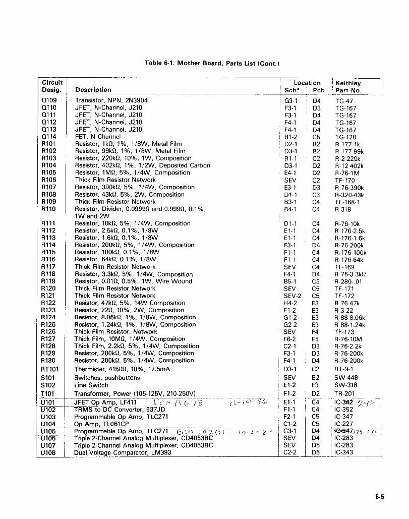
Table 6-1. Mother Board, Parts List (Cont.)
Circui Desig
Q109 QIIO 0111 a112 a113 cl114 RIO1 R102 R103 R104 RI05 RI06 RI07 RI08 RI09 RI10
RI11 Rl12 Rl13 R114 RI15 R116 RI17 RI18 RI19 R120 RI21 A122 RI23 RI24 RI25 RI26 RI27 RI28 RI29 R130
RTIOI SIOI s102 TIOI
E u102 u103 u104 u105 U106 u107 UlO8
Description
Transistor, NPN, 2N3904 JFET, N-Channel, J210 JFET, N-Channel, J210 JFET, N-Channel, J210 JFET, N-Channel, J210 FET, N-Channel Resistor, lkn, 1%. 1 l8W. Metal Film Resistor, 99kR. I%, l/EW, Metal Film Resistor, 220kR. 10%. lW, Composition Resistor, 402kI2, 1%. 1 l2W. Deposited Carbon Resistor, 1 Mfl, 5%, 1 l4W. Composition Thick Film Resistor Network Resistor, 390k12. 5%. 1/4W, Composition Resistor, 43kO. 5%, 2W, Composition Thick Film Resistor Network Resistor, Divider, 0.0999Q and 0.9990, 0.1% IW and 2W Resistor, IOkiI, 5%, lI4W. Composition Resistor, 2.5kR, 0.1%. 1/8W Resistor, 1.6k0, 0.1%. 118W Resistor, 200kn. 5%. lI4W. Composition Resistor, IOOkQ, 0.1%. l/EW Resistor, 64kn. 0.1%. l/EW, Thick Film Resistor Network Resistor, 3.3kR. 5%. 1/4W. Composition Resistor, O.Olfl, 0.5%. 1W. Wire Wound Thick Film Resistor Network Thick Film Resistor Network Resistor, 47k0, 5%. 14W Composition Resistor, 220, 10%. 2W. Composition Resistor, 8.06k12, 1%. l/EW, Composition Resistor, 1.24kfl. I%, 1 IEW, Composition Thick Film Resistor, Network Thick Film, IOMn, 1/4W, Composition Thick Film, 2.2k0, 5%. 114W. Composition Resistor, 200k0, 5%. 1 l4W. Composition Resistor, 200k0, 5%. 114W. Composition
Thermister, 41500, 10%. 17.5mA
Switches, pushbuttons Line Switch
Transformer, Power 1105.125V, 210.25OV) JFET Op Amp, LF411 Ii ~C I- 1~1~ b ./ r: TRMS to DC Converter, 637JD Programmable Op Amp, TLC271
I G3-1 D4 ~ F3-1 D3
F3-1 D4 F4- 1 D4 F4-1 D4
~ 81-2 c5 ~ D2-1 82
D3-1 82 81-l c2 D3-1 D2
T&e 2-Channel Analoa Multiblexer; CD4053BC Dual Voltage Comparator, LM393
E4- 1 SEV E3-1 Dl~l 83-l B4-1
Dl-1 El-l El-l F3-1 Fl-1 Fl~l SEV F4- 1 85.1 SEV SEV-2 H4-2 Fl-2 Gl-2
c5 E3 E3 E3 E3 F4 F5 D3 D3 D4
G2-2 SEV F6-2 c2-1 F3- 1 F4- 1
D3-1 SEV El-2 Fl-2 El-l Fl-1 F2-1
c2 82 F3 D2
TF-172 R~76-47k R-3-22 R-88.8.06k R~88-1.24k TF-173 R-76.10M R-76.2.2k R-76.200k R-76.200k RT-9-l SW-448 SW-318 TR-201
Cl-2 c5 i IC-227 G3-1 D4 SEV D4
I e&t7,7; -c~cL’; ) IC-283
SEV D5 ~ IC-283 C2-2 D5 : IO-343 -i--
D2 C2 03 c3 c4 c4
c4 c4 c4 04 c4 c4 c4 D4
1Keithley Part No.
TG-47 TG-167 TG-167 TG~l67 TG-167 TG-128 R~l77~lk R-177.99k R-2.220k R-12~402k R-76.1M TF-170 R~76-390k R-320-43k TF-168-l R-318
R-76.10k R-176.2.5k R-176.1.6k A-76~200k R-176.IOOk R-176.64k TF~l69 R~76-3.3klf
6-6

Table 6-l. Mother Board, Parts List (Cont.)
Circuit Location Keithley Desig. Description Sch* Pcb Part No.
u109 Triple 2.Channel Analog Multiplexer, CD4053BC SEV D3 K-283 UllO 16 x 16 Bit Serial Nonvolatile Static RAM, X2443P H4-2 D4 IO-353 Ulll Hex Inverter, 74HC04 D5-1 D4 ic-354 u112 Quad 2-Input NAND Gate, 74HCOO WI D4 IC-351 u113 ~ 1024 x 4 Bit Static CMOS RAM A5-2 D5 LSI-62 u114 Peripheral Interface Adapter, 65C21 83.2 E4 LSI-61 u115 8k x 8 UV Erasable PROM 85-2 E5 175-EOO-” U116 Regulator, + 5V. IA, 7805 Gl-2 E3 IC-93 u117 3.Terminal Adjustable Regulator, LM337L G2-2 E3 IC-345 U118 Triple 3.Input OR Gate, CD4075BE SEV E3 IC-143 u119 Triple 3.Input NAND Gate, MM74HClO SEV E4 IC-341 u120 Tri-State Octal D Latch, 74HC373 D5-2 E5 IC-338 u121 Dual D Flip-Flop, 74HC74 E2-2 F3 IC-337 u122 12 Stage Binary Counter, 40408 D3-2 F4 IC-348 U123 CMOS E-Bit Microprocessor, 146805E2 F3-2 F5 LSI-60 VRIOI Diode, Zener, 6.35V. 400mW. lN4577 F2-1 C5 DZ-58 VR102 Diode, Zener, 12V. 5W. lN5349 Gl-2 E3 DZ-72-l VR103 Diode, Zener. 5.lV. 400mW. lN751 G2-1 C5 DZ-59 VR104 Diode, Zener, 12V. 1 N963B Hl-2 D3 DZ-54 WlOl Calibration Jumper, Connector H5-2 D4 CS-476 YlOl Crystal. 3.2768MHz E6-2 F5 CR-21
‘“Order same software as presently installed. For example, if Al is the displayed software order 175.800.Al.
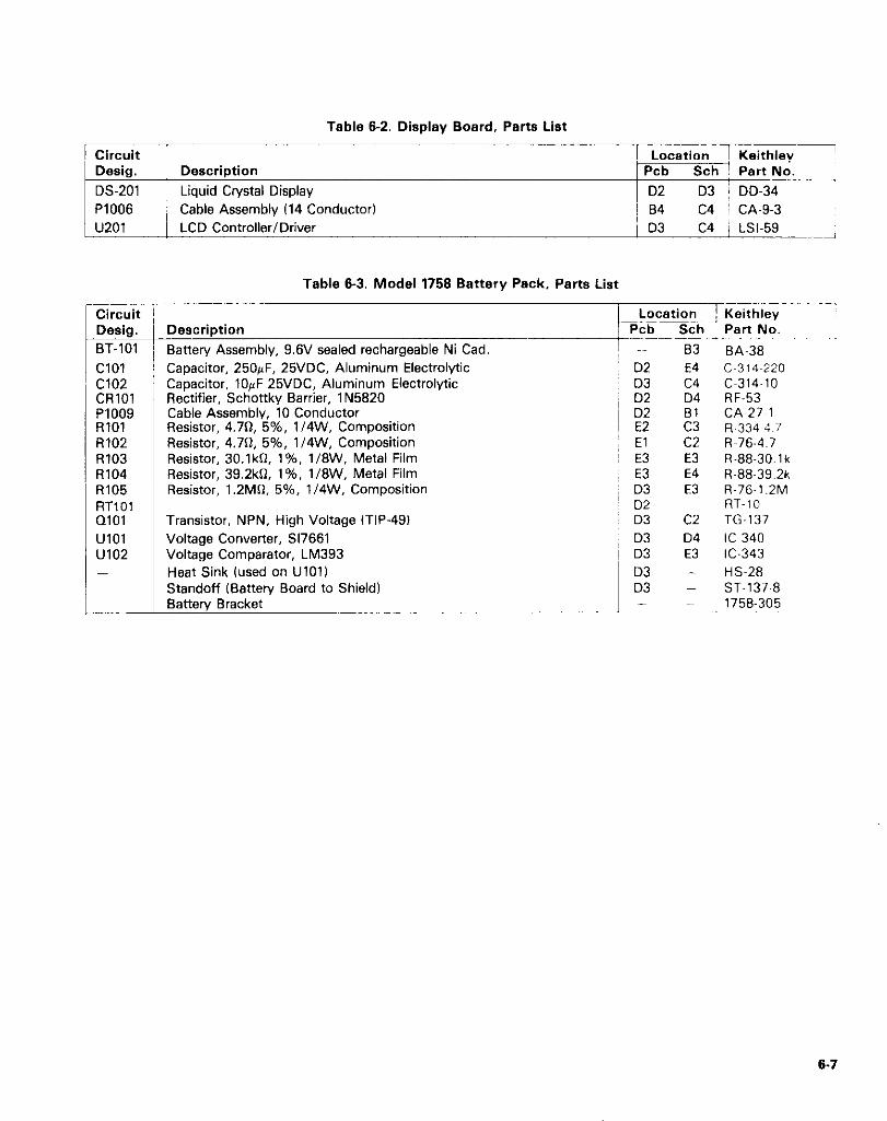
Table 6-2. Display Board, Parts List
Circuit Desig.
DS-201 PI006 u201
Description
Liquid Crystal Display Cable Assembly 114 Conductor1 LCD Controller/Driver
etigy ;,“;h&y
D2 D3 ~ DD-34
I 84 C4 i CA-g-3 i D3 C4 j LSI-59
Table 6-3. Model 1756 Battery Pack, Parts List
Circuit Desig.
BT-101
Cl01 Cl02 CR101 PI009 I3101 RI02 R103 R104 R105 RT101 QIOI UIOI u102 -
Description
Battery Assembly, 9.6V sealed rechargeable Ni Cad. Capacitor, 25OpF. 25VDC, Aluminum Electrolflic Capacitor, 1OrF 25VDC, Aluminum Electrolytic Rectifier, Schottky Barrier, 1 N5620 Cable Assembly, 10 Conductor Resistor, 4.70. 5%. ll4W. Composition Resistor, 4.70, 5%, 114W. Composition Resistor, 30.lk0, I%, l/EW. Metal Film Resistor, 39.2k0, 1%. IKIW, Metal Film Resistor, 1.2MR. 5%. 114W. Composition
Transistor, NPN, High Voltage (TIP-491 Voltage Converter, Sl7661 Voltage Comparator, LM393 Heat Sink (used on UlOl) Standoff (Battery Board to Shield1 Battery Bracket
D2 D3 D2 D2 E2 El E3 E3 03 D2 D3 03 D3
03 03 -
Location jKeithley Pcb Sch Part No.
83 EA.38 E4 C~314~220 c4 C~314.10 D4 RF-53
:; CA~27~1 R.334~4~7
c2 R~76-4.7 E3 R-IX-30.1k E4 R-68~39.2k E3 R-76.1.2M
RT-10 c2 TG-137 D4 IC~340 E3 IC-343
HS28 ST-137-8 1758.305
6-7

Table 6-4. Model 175 Spare Parts List
Qty 4 2 1 1 5
1 2 4
1 1 1 1 2 1 1 1 1 1 1 1
Keithley Part No.
FU-13 FU-20 RL-62 RL-59 TG-62
TG-166 TG-138 TG-167
TG-128 RT-9-l IC-352 IC-347 IC-283 IC-353 IC-354 IC-351 IC-93
IC-345 DZ-58
DZ-72-1
Circuit Desig.
FlOl F102 KIOI
K102-K103 0102, Q104, Q105,
Q107, Q108 Q106 a103
QIIO, Qlll, Q112, Q113 0114
RTlOl u102
u103, u105 U106,U107, U109
UIIO Ulll u112 U116 u117
VRlOl VR102

6-S/6-10

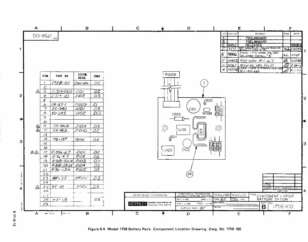
1
2
4
I I I I F
Figure 6-4. Model 1756 Battery Pack. Component Location Drawing, Dwg. No. 1756-100


-
-
-
-
-
Figure 6-5. Mother Board. Component Location Drswing. Dwg. No. 175100 (Page 1 of 21
6-13/6-14

” “113 J
Figure 6-5. Mother Board. Component Location Drawing. Dwg. No. 175100 IPsge 2 of 21
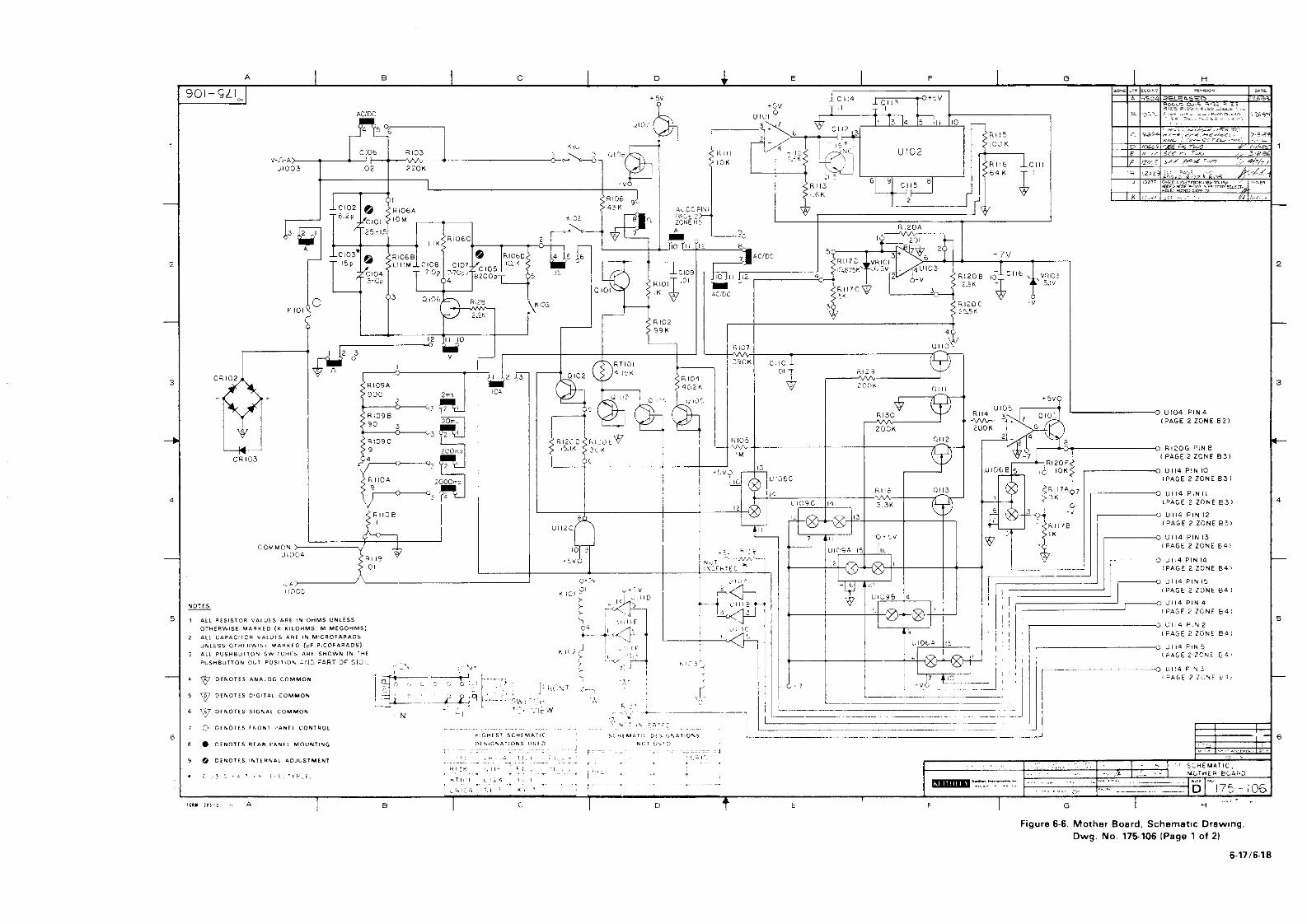
1
2
-
3
i
4
-
-
t
c
2
3
+-
4
6
I I ci
I Go.
I L1 I t I 0 I n
Figure 6-6. Mother Board. Schematic Drawng. Dwg. No, 175106 [Page 1 of 21
6-171618

I I I II
Figure 6-6. Mother Board. Schematic Drawing. Dwg. No 175.106 (Page 2 of 21
6.19/6-20

CONTACT DESCRIPTION
X3/6-24
SERVICE FORM Model No. Serial No. Name and Telephone No. Company
List all control settings. describe problem and check boxes that apply to problem.
Date
q Intermittent q Analog output follows display q Particular range or function bad; specify q IEEE failure q Obvious problem on power-up q Batteries and fuses are OK OFroot panel operational OAll ranges or functions are bad q Checked all cables
Display or output (circle one)
aDrifts q lJnable to zero q IJnstable q Will not read applied input q OverIoad
q Calibration only q Data required
UC of C required
(attach any additional sheets as necessary.)
Show a block diagram of your measurement system including all instruments connected (whether power is turned on or not). Also, describe signal source.
Where is the measurement being performed? (factory. controlled laboratory, out-of-doors, etc.)
What power line voltage is used? Ambient Temperature?
Relative humidity? Other?
Any additional information. (If special modifications have been made by the user. please describe.)