Embed Size (px)
Citation preview

Instruction Manual Model 193A
System DMM
01985, Keithley Instruments, Inc. Instrument Division
Cleveland, Ohio, U.S.A. Document Number 193A-901-01


SAFETY PRECAUTIONS
The following safety precautions should be observed before operating the Model ~193A
This instrument is intended for use by qualified personnel who recognize shock huxds .~nd are i,lmiliar with the safety precautions required to avoid possible injury. Read WET the manual carefully before operating this instrument.
Exercise extreme caution when a shock hazard is present at the instrument’s input. The American National Standards Institute (ANSI) states that a shock hazards exists when voltage levels greater than 3OV rms or 42.4V peak are present. A good safety practice is to expect that a hazardous voltage is present in any unknown circuit before measuring.
Ins .R
ect the test leads for possible wear, cracks or breaks before each use. If any defects are found, replxe wt test leads that have the same measure of safety as those supplied with the instrument.
For optimum safety do not touch the test leads or the instrument while power is applied to the circuit under test. Turn the power off and discharge all capacitors, before connecting or disconnecting the instrunwnt. Always disconnect all unused test leads from the instrument.
Do not touch any object which could provide a current path to the common side of the circuit under lest or power line (earth) ground. Always make measurements with dry hands while standing on ‘1 dry, ill- s&ted surface, capable of withstanding the voltage being measured.
Exercise extreme safety when testing high energy power circuits (AC line or mains, etc). Refer to the t ligh Energy Circuit Safety Precautions found in paragraph 2.6 (Basic Measurements).
Do not exceed the instrument’s maximum allowable input as defined in the specifications and operation section.


SPECIFICATIONS
DC VOLTS ACCURACY (5% Digits)” TEMPERATURE MAXIMUM * t%rdg + counts) COEFFICIENT READING RESOLUTION INPUT 24 Hr., 90 Days, 1 Yr.,
ANALOG 1 it%rdg+countsli~~ C SETTLING ~
RANGE (5% Digits) 6% 5% RESISTANCE 23O+l”C 23’*5T 23’f5”C O”-18’C & 28--5O~C TIME”* i
200mV 219.999mV 10” n” 1 IrV >lCX 0.003+2* 0.005+2’ 0.00x+2* o.wK? in 1 < zms 2 V 2.19999 V 1 $V lop” >lCx 0.002+ 1 0.005+2 0.007+2 (l.WOS +~ 0. I < 1,115
20 V 21.9999 V 10 &V 100 &V 1OMCl 0.003+ 1 0.007+1 0.009+3 (1.lx)O7+O.l < I”,> 200 V 219.999 V 100 ,,V lm” 1OMR 0.003+1 O.O07+l 0.009+3 O.WO7 +o. I < lms
1000 v 1000.00 v 1mV 1OmV 1OMR 0.004+1 0.007+1 0.009+5 0.0007+0.1 < I”,5 *When properly zeroed. **Multiply digit error by 10 for h%~digit accuracy. “‘To (1.01% of step ch.qe.
NMRR: Greater than 60dB at 50 or 60Hr. MAXIMUM MEASUREMENT RATES (into internal CMRR: Greater than 120dB at dc and 50 or 6OHz memory, filter and multiplex off):
(with lk0 in either lead). 3% Digit 4% Digit 5% Digit 6’12 Digit MAXIMUM ALLOWABLE INPUT: 1OOOV peak. 1000 rdgis 333 rdgls 25 rdg:s 25 rdg s
TRMS AC VOLTS (Option 1930) MAXIMUM ACCURACY (5% Digits)‘*’
READING RESOLUTION + t%rdg + counts, 1 Year, 18’.28 c
RANGE (5% Digits) 6% 5% 20Hz-50Hz’ 50Hz-IOkHz’ IOkHz-20kHz’ ZOkHz-100kHz”
2" 2.19999" 1 Ir” 10 pv 1 + 100 0.25+ I(10 11.35 + 300 I f so0 2ov 21.9999" 10 /Lv 100 flv 1+ 100 0.25+100 L1.35 + SW I f xx1
2oov 219.999" 100 PV 1mV 1+ 100 0.25+ 100 13.31+ 3Nl I _ 3ki 700" 700.00 v 1mV lOmV 1+100 0.35+100 0.5 4~ SW I + SiHl
*Above 2000 COUPES. **Above 20000 counts; 3%+500 typical below 20000. “‘Multiply digit erwr by ill for 6’.:-digit .~cur.xy. ~
RESPONSE: True root mean square, ac or ac+dc. 3dB BANDWIDTH: 500kHr typical. !
CREST FACTOR: Rated accuracy to 3. Specified for CMRR: Greater than 6OdB at 50 and 6OHr (Ikl2 1111. ~ pulse widths > lops, peak voltage 5 1.36 x full scale. balance).
AC+DC: Add 60 counts to specified accuracy. dBV (Ref. = 1V): ACCURACY +dBV
MAXIMUM INPUT: 1OOOV peak ac + dc, 2 x lO’V*Hr. 1 Year. In~-zn c
SETTLING TIME: 0.5s to within 0.1% of change in INPUT ZOHz-ZOkHz ZOkHz-1WkHr RESOLUTION
reading. 14 to +57dHV
INPUT IMPEDANCE: 1Mfi shunted by less than 120pF. (2OOmV t* 7WV rms) 0.2 11.4 ,J OldH\’
TEMPERATURE COEFFICIENT CO’=-18°C & 28’-50°C): -34 to 14dUV Less than *(0.1x applicable accuracy specification)i”C (20mV t0 2OOmV) I .s S’ i)~illdH\
below 50kH.z; (0.2x) for 50kHz to 100kHr. ‘Typical
200mv 100 pv 2+3 2" ImV 2+3
20 v 1OmV 2+3 200 v 100mV 2+3 700 v 1 v 2+3
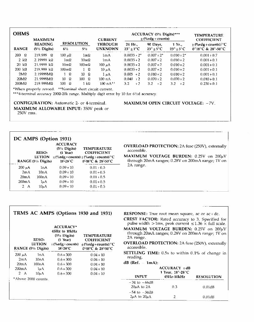
OHMS ACCURACY (5% Digits)***
MAXIMUM CURRENT -t (%rdg + counts)
READING RESOLUTION THROUGH 24 Hr., 90 Days, 1 Yr., RANGE (5% Digits) 6% 5’,2 UNKNOWN 230 * 1°C 23’ i ST 230 i5T
200 n 219.999 n 100 po lmfl ImA 0.0035+2* 0.007+2* 0.010+2* 2 kO 2.19999 k!I ImIl 1Omfl ImA 0.0035+2 0.007+2 0.010+2
20 kn 21.YYYY k0 Nllll~ 1oomn 100 &A 0.0035+2 0.007+2 0.010+2 200 kR 219.999 kll 1OOmR 1 n 10 I”A 0.0035+2 0.007+2 0.010+2
2Mfl 2:19999Mn 1 R ‘IO n 14 0.005 +2 0.010+2 Ll.o10+2 20Mll 21.9999MQ 10 n 100 a 100 nA 0.040 +2 0.070+2 0.070~2
200Mn 21Y.YY9Mn 100 R 1 kn 100 nA** 3.2 +2 3.2 +2 3.2 +2
*When properly zeroed. **Nominal short circuit current. ***4-terminal accuracy 200S20k range. Multiply digit error by 10 for 6’/zd accuracy.
TEMPERATURE COEFFICIENT
*(%rdg+counts)/“C O”lBoC & 28’-5O’C
0.001+0.7 0.001+ 0.1 0.001+0.1 0.001+0.1 0.001+0:1 0.010+0:1 0.230+0.1
CONFIGURATION: Automatic 2. or 4.terminal.
MAXIMUM ALLOWABLE INPUT: 350V peak or 250V rms.
MAXIMUM OPEN CIRCUIT VOLTAGE: 7V
DC AMPS (Option 1931) ACCURACY (5% Digits) (S/2 v,ges, 1 TEMPERATURE
RESO- RESO- (1 Year) (1 Year) COEFFICIENT LUTION *(%rdg+counts)*( LUTION *(%rdg+counts) -t(%rdg+counts)i”C
RANGE 15% Dieits) RANGE (5% Digits) 18*28”C 18*28”C 0’ 00-18T & 280-SOT
200 pA InA 0.09+10 0.01+0.5
OVERLOAD PROTECTION: 2A fuse (25OV), externally accessible.
MAXIMUM VOLTAGE BURDEN: 0.25V on 200pV through 20mA ranges; 0.28V on 200mA range; 1V on 2A range.
2mA 10nA 0.09+10 0.01+0.5 20mA lOOnA 0.091-10 0.01+0.5
200mA l@A 0.09+10 0.01+0.5 2 A lo+4 o.o9+1O 0.01+0.5
TRMS AC AMPS (Options 1930 and 1931)
ACCURACY* 45Hz to 1OkHz
(5% Digits) TEMPERATURE RESO- (1 Year) COEFFICIENT
LUTION +(%rdg+counts) -t(%rdg+counts)/“C RANGE (5% Digits) 180-28°C 0”-18”C & 28%5O’C
GO fill ‘InA 0.6+300 0.04+10 2mA 1OnA 0.6+300 0.04+10
20mA IOOnA 0.6+300 0.04+10 200mA ‘IpA 0.6+300 0.04+10
2 A 10fiA 0.6+300 0.04+10 *Abwc 2000 counts.
RESPONSE: True root mean square, ac or ac+dc.
CREST FACTOR: Rated accuracy to 3. Specified for pulse width > lms, peak current 5 1.36 x full scale.
MAXIMUM VOLTAGE BURDEN: 0.25V on 2OOpV through 20mA ranges; 0.28V on 200mA range; 1V on 2A range.
OVERLOAD PROTECTION: 2A fuse (25OV), externally accessible.
SETTLING TIME: 0.5s to within 0.1% of change in reading.
dB (Ref. = ImA): ACCURACY + dB 1 Year, 18O-28°C
INPUT 45Hz-10kHz RESOLUTION
-34 to +66dB 20pA to 2A
-54 to -34dB 2pA t” 20/~/I
0.3 O.O~ldB
2 O.OldU

TEMPERATURE (Thermocouple) (over IEEE Blrs only) THERMO- ACCURACY= COUPLE (1 Year)
TYPE RANGE RESOLUTION 113°-28”C
J -100 to + 760°C O.l”C 10.5”C K -100 t” +1372”C O.l”C +0.5”C T -100 to + 400°C O.l”C +0.5oc E - 100 to + 1000°C O.l”C kO.h”C R 0 to +1768”C 1 “C *3 “C s 0 to c176PC 1 “C *3 “C B c350 t” +1821”C 1 “C 1-5 “C
‘Relative to external 0°C reference junction; exclusive of ther- mocouple errors. Junction temperature may be external.
TEMPERATURE (RTD) 4-WIRE
RESO- ACCURACY* TEMPERATURE RANGE LUTION 1 Yr., 18°-2~oC COEFFICIENT
1000 to O.Ol"C *o.lt?"c
* (0.0013% + +63O”C O.O05~C)/~C
148O to O.Ol”F 10.36OF *(0.0013%+ +llOO”F 0.01 ‘F)PC
*Excluding probe errors.
RTD TYPE: 1000 platinum; DIN 43 760 or IPTS-68, alpha 0.00385 or 0.00392, 4.wire.
MAXIMUM LEAD RESISTANCE (each lead): 4.wire, 10R.
SENSOR CURRENT: 1mA COMMON MODE REJECTION: Less than 0.005”CIV at
dc, 50Hz and 60Hz (lOOn unbalance, LO driven). MAXIMUM ALLOWABLE INPUT: 350V peak, 250V
*Ins.
IEEE-488 BUS IMPLEMENTATION Multiline Commands: DCL, LLO, SDC, GET, GTL,
UNT, UNL, SI’E, SI’D. Uniline Commands: IFC, REN, EOI, SRQ, ATN. Interface Functions: SHl, AHl, TEO, LA, LEO, SRl, RLZ,
PPO, DCl, DTl, CO, El. I’rogrammable Parameters: Range, Function, Zero, Inte-
gration Period, Filter, dB Reference, EOI, Trigger, Ter- minator, Delay, 500-rd
P Storage, Scaling, Calibration,
Display, Multiplex Of, Status, Service Request, Self Test, Output Format.
GENERAL DISPLAY: 14, 0.5.in. alphanumeric LED digits \vith
decimal point and polarity. Function and IEEE bus status also displayed.
RANGING: Manual or fast autoranging. ISOLATION: Input LO to IEEE LO or power line
ground: 500V max., 5xlOSV.Hz; greater than ~10% paralleled by 400pF.
DATA MEMORY: I to 500 locations, progrumwble, Measurement intervals selectablr lms to 999.999x-c or triggered.
BENCH READING RATE: 5 readingswr, vwpt 2O~lIl; ZOOMR range 2 rcadingsisec.
ZERO: Control subtracts on-scale value from subsequent readings or allows value to bc programmed.
FILTER: Weighted average (exponential). Programmable weighting: 1 to &
WARMUP: 1 hour to rated accuracy. OPERATING ENVIRONMENT: [I’,-50 C’, 0% to 809,
relative humidity up to 35’C; linearly derate 3% RH/“C, 35°C to 50°C (except 2OOMII range: 0% TV, M1”,> RH up to 28°C).
STORAGE ENVIRONMENT: -25~~ to +65-C. POWER: 105.725V or 210.250V (internal switch selected),
50Hz or 6OHz, 40VA maximum 90.I~ItlV & 180.22O\’ versions available upon request.
CONNECTORS: Analog: Switch selectable front (lr rear, safety input jacks. Digital: TRIGGER input and \‘(>I-.I- METER COMPLETE output on rear panel, BSCs.
DIMENSIONS, WEIGHT: 89mm high x 43Hmm wide x 441mm deep (3% in. x ~17% in. x 171% in.). Set weight 33kg (15 Ibs.).
ACCESSORlES AVAILABLE: Model 1600A: Hi h Voltage Probe Model 1641: K&n Test Lead Set Model 1651: 50.Ampere Shunt Model 1681: Clip-On Test Lead Set Model 1682A: RF Probe Model 1685: Clamp-On Current Probe Model 1751: General Purpose Test Leads Model 1754: Universal Test Lead Kit Model 1930: True RMS ACV Option Model 1931: Current Option Model 1938: Fixed Rack Mounting Kit Model 1939: Slide Rack Mounting Kit Model 7007-l: Shielded IEEE-488 Cable, lm Model 7007-2: Shielded IEEE-488 Cable, 2m Model 7008.3: IEEE-488 Cable, 3 ft. (0.9m) Model 7008.6: IEEE-488 Cable, 6 ft. (1.8m)
Specifications subject to change without notice,


TABLE OF CONTENTS
SECTION l-GENERAL INFORMATION
1.1 INTRODUCTION ............................................................................ 1-l 1.2 FEATURES .................................................................................. 1-l 1.3 WARRANTY INFORMATION ................................................................. I-1 1.4 MANUAL ADDENDA ....................................................................... l-l 1.5 SAFETY SYMBOLS AND TERMS ............................................................. l-1 1.6 SPECIFICATIONS ........................................................................... 1-2 1.7 INSPECTION ............................................................................... l-2 1.8 USING THE MODEL 193A MANUAL, ........................................................ l-2 1.9 GETTING STARTED ......................................................................... 1-2 1.10 ACCESSORIES .............................................................................. 1-3
SECTION 2-BASIC DMM OPERATIONS
2.1 2.2 22.1 2.2.2 2.2.3 2.2.4 2.3 2.3.1 2.3.2 2.3.3 2.3.4 2.4 2.4.1 2.4.2 2.4.3 2.5 2.6 2.6.1 2.6.2 2.6.3 2.6.4 2.6.5 2.6.6 2.6.7 2.6.8 2.6.9 2.6.10 2.6.11 2.6.12 2.6.13 2.7 2.7.1 2.7.2 2.8 2.8.1 2.82
INTRODUCTION ........................................................................... 2-l POWER UPPROCEDURES ................................................................... 2-l
Line Power ................................................................................ 2-l rower-up Sequence ........................................................................ 2-I Factory Default Conditions ................................................................. 2-I User Programmed Conditions .............................................................. 2.2
FRONT PANEL FAMILIARIZATION .......................................................... 2-2 DisplayandIndicators ..................................................................... 2-2 Controls.. ................................................................................ 2.2 Input Terminals ........................................................................... 2-4 Current Fuse .............................................................................. 2-4
REAR PANEL FAMILIARIZATION ............................................................ 2-3 Connectors and Terminals .................................................................. 2-4 Calibration Switch ......................................................................... 2-5 Line Fuse ................................................................................. 2-S
ERROR AND WARNING DISPLAY MESSAGES ............................................... 2-5 BASICMEASUREMENTS .................................................................... 2-Y
Warm Up Period .......................................................................... 2-Y Zero ...................................................................................... 2-Y Filter ..................................................................................... 2-11 DC Voltage Measurements ................................................................. 2-12 Low-Level Measurement Considerations., ................................................... Z-13 TRMS AC Voltage Measurements. .......................................................... 2.14 Resistance Measurements .................................................................. 2-15 Current Measurements (DC or TRMS AC) .................................................. 2-16 RTD Temperature Measurements ........................................................... 2.17 dBMeasurements ......................................................................... 2.17 dB Measurement Considerations and Applications,, ......................................... 2-19 TRMS AC + DC Measurements ............................................................ 2-19 TRMS Conslderatmns ....................................................................... Z-20
DATA STORE .............................................................................. 2-22 Storing Data ............................................................................. 2-22 Recalling Data ............................................................................ 2-23
FRONT PANEL PROGRAMS ................................................................ 2.25 Cursor and Data Entry, ................................................................... 2-25 ProgramTEMP ........................................................................... 2-25
i

2.8.3 2.8.4 2.8.5 2.8.6 2.8.7 2.8.8 2.8.9 2.8.10 2.8.11 2.8.12 2.8.13 2.8.14 2.8.15 2.9 2.10 2.10.1 2.10.2 2.10.3
Program AC + DC (Low Frequency AC). Program dB ........................... Program ZERO ........................ Program FILTER ....................... Program RESET ....................... Program4 ............................ Program 90 (Save) ..................... Program 91 (IEEE Address) ............. Program 92 (Freq) ..................... Program 93 (Diagnostics). .............. Program 94 (MX + B Status) ........... Program 95 (Multiplexer) ............... Program 96 (CAL) .....................
FRONT PANEL TRIGGERING ........... EXTERNAL TRIGGERING ...............
External Trigger ....................... Voltmeter Complete. ................... Triggering Example ....................
..........
..........
..........
..........
..........
..........
..........
..........
..........
..........
..........
..........
..........
..........
..........
..........
..........
..........
..........
..........
..........
..........
..........
..........
..........
..........
..........
..........
..........
..........
..........
..........
..........
..........
..........
..........
............. 2-25
............. Z-26
............. 2-26
............. Z-26 ............................ 2-27 ............................ 2-27
......
......
......
......
......
......
......
......
......
......
......
......
......
......
......
......
...... 2.28
...... 2.29
...... 2.29
...... 2-29
...... 2.29
...... Z-30
...... 2-30
...... 2-30
...... 2-31
...... 2-31
...... 2-31
...... 2.32
SECTION 3-IEEE-488 PROGRAMMING
3.1 3.2 3.3 3.3.1 3.3.2 3.3.3 3.4 3.4.1 3.4.2 3.4.3 3.4.4 3.4.5 3.5 3.6 3.6.1 3.6.2 3.6.3 3.7 3.7.1 3.7.2 3.7.3 3.8 3.8.1 3.8.2 3.8.3 3.8.4 3.9 3.9.1 3.9.2 3.9.3 3.9.4 3.9.5 3.9.6 3.9.7 3.9.8 3.10
ii
INTRODUCTION ........................................................................... 3-l BUS DESCRIPTION.. ....................................................................... 3-l IEEE-488 BUS LINES ........................................................................ 3-2
Data Lines ................................................................................ 3-2 Bus Management Lines .................................................................... 3-2 Handshake Lines .......................................................................... 3-2
BUS COMMANDS .......................................................................... 3-3 Uniline Commands.. ... . .................................................................. 3-4 Universal Commands.. .................................................................... 3-4 AddressedCommands ..................................................................... 3-5 Unaddressedcommands ................................................................... 3-5 Device-Dependent Commands .............................................................. 3-5
COMMAND CODES ........................................................................ 3-5 COMMAND SEQUENCES ................................................................... 3-7
Addressed Command Sequence ............................................................. 3-7 Universal Command Sequence .............................................................. 3-7 Device-Dependent Command Sequence ..................................................... 3-7
HARDWARE CONSIDERATIONS ............................................................. 3-7 Typical Controlled Systems ................................................................. 3-7 BusConnections .......................................................................... 3-8 Primary Address Programming. ............................................................ 3.10
SOFTWARE CONSIDERATIONS ............................................................. 3.10 Controller Handler Software ............................................................... 3-10 Interface BASIC Programming Statements ................................................... 3.10 Interface Function Codes .................................................................. 3-11 IEEE Command Groups ................................................................... 3.12
GENERAL BUS COMMAND PROGRAMMING. .............................................. 3-12 REN(RemoteEnable) ..................................................................... 3.1~2 IFC(InterfaceClear) ....................................................................... 3.13 LLO(IocalLockout) ...................................................................... 3.13 GTL (Go To Local) and Local .............................................................. 3.13 DCL(DeviceClear) ....................................................................... 3-n SDC(Send Device Clear) .................................................................. 3-14 GET (Group Execute Trigger) .............................................................. 3-14 Serial Polling (SPE, SPD) .................................................................. 3.14
DEVICE-DEPENDENT COMMAND PROGRAMMING ......................................... 3-15

3.10.1 3.10.2 3.10.3 3.10.4 3.10.5 3.10.6 3.10.7 3.10.8 3.10.9 3.10.10 3.10.11 3.10.12 3.10.13 3.10.14 3.10.15 3.10.16 3.10.17 3.10.18 3.10.19 3.10.20 3.10.21 3.10.22 3.10.23 3.11 3.11.1 3.11.2 3.12 3.13 3.x3.1 3.X3.2 3.13.3 3.w.4 3.x3.5 3.X3.6 3.w.7 3.13.8 3.x3.9
Execute(X) ............................................................................... 3.19 Function(F) .............................................................................. 3-1~ Range(R) ................................................................................ 3-19 Zero(Z) ................................................................................. 3-20 Filter(P)............................................................................~ .... 3.20 Rate(S) .................................................................................. 3.21 Trigger Mode (T) ......................................................................... 3.21 Reading Mode(B) ........................................................................ 3.22 Data Store Interval (Q) and Size (1) ........................................................ 3.22 Value (V) and Calibration (C) .............................................................. 3.23 Default Conditions (L) .................................................................... 3.24 Data Format(G) .......................................................................... 3-24 SRQ Mask (M) and Status Byte Format. .................................................... 3.25 EOI and Bus Hold-Off Modes (K) .......................................................... 3.28 Terminator (Y) ............................................................................ 3.28 Status(U) ............................................................................... 3.2’) Multiplex (A) ..................................................................... ... ~, 3.33 Delay(W) ............................................................................... 3.33 Self-Test(J) ............................................................................... R-33 Hit Button(H) ........................................................................... 3-3-1 Display(D) .............................................................................. 3-W Reference Junction (0) .................................................................... 3-35 Exponential Filter (N) ..................................................................... 3.36
FRONT PANEL MESSAGES ................................................................. 3.36 Bus Error ................................................................................ 3-36 Trigger Overrun Error ..................................................................... 3.37
BUS DATA TRANSMISSION TIMES ......................................................... 3.37 TRANSLATOR SOFTWARE ................................................................. 3-37
Translator Format ......................................................................... 3.37 Wild Card($) ............................................................................... 3-3’)
NEW and OLD .......................................................................... 3-39 Combining Translator Words .............................................................. 3-3’) Combining Translator Words with Keithley IEEE-488 Commands .............................. 3-40 Executing Translator Words and Keithley IEEE Commands ......................... ......... 3-40 SAVE .................................................................................... 3-41 LIST ..................................................................................... 3-41 FORGET ................................................................................. 3.41
SECTION 4-PERFORMANCE VERIFICATION
4.1 4.2 4.3 4.4 4.5 4.5.1 4.5.2 4.5.3 4.5.4 4.55 4.5.6
INTRODUCTION ........................................................................... 4-l ENVIRONMENTALCONDITIONS ............................................................ 1-1 INITIAL CONDITIONS.. .................................................................... 4-l RECOMMENDED TEST EQUIPMENT. ........................................................ 4-I VERIFICATION PROCEDURES ...................................................... ........ 4-I
DC Volts Verification.. ..................................................................... 1-2 TRMS AC Volts Verification ................................................................. 4-3 OHMS Verification ........................................................................ 4-4 DC Current Verification .................................................................... 4-5 TRMS AC Current Verification .............................................................. 4-h RTD Temperature Verification ............................................................. 4-7
SECTION 5-THEORY OF OPERATION
5.1 INTRODUCTION ..,,...........,......,....,.,,.,...................................~....~. 5-l
iii

5.2 OVERALL FUNCTIONAL DESCRIIJTION ..................................................... 5-l 5.3 ANALOG CIRCUITRY ....................................................................... 5-l
5.3.1 Input Signal Conditioning .................................................................. 5-l 5.3.2 Multiplexer ............................................................................... 5-6 5.3.3 +Z.lV Reference Source .................................................................... 5-8 5.3.4 Input Buffer Amplifier ..................................................................... 5-8 5.4 AIDCONVERTER ........................................................................... 5-8 5.5 CONTROLCIRCUITRY.. ................................................................... 5-10 5.6 DIGITAL CIRCUITRY ....................................................................... 5-10 5.6.1 Microcomputer ........................................................................... 5-10 5.6.2 Display Circuitry .......................................................................... 5-10 5.7 POWER SUPPLIES ......................................................................... 5-10
SECTION 6-MAINTENANCE
6.1 INTRODUCTION ........................................................................... 6-l 6.2 LINE VOLTAGE SELECTION ................................................................. 6-l 6.3 FUSEREPLACEMENT ....................................................................... 6-l 6.3.1 Line Fuse ................................................................................. 6-l 6.3.2 Current Fuse. ............................................................................. 6-2 6.4 MODEL 1930 TRMS ACV OPTION INSTALLATION ............................................ 6-2 6.5 MODEL 1931 CURRENT OPTION INSTALLATION ............................................ 6-3 6.6 CALIBRATION .............................................................................. 6-3 6.6.1 Recommended Calibration Equipment ....................................................... 6-3 6.6.2 Environmental Conditions .................................................................. 6-3 6.6.3 Warm-Up Period .......................................................................... 6-3 6.6.4 Calibration Switch ......................................................................... 6-5 6.6.5 Front Panel Calibration. .................................................................... 6-5 6.6.6 IEEE-488 Bus Calibration ................................................................... 6-6 6.6.7 Calibration Sequence ....................................................................... 6-7 6.68 DC Volts Calibration ....................................................................... 6-7 6.6.9 Resistance Calibration ...................................................................... 6-8 6.6.10 TRMS AC Volts Calibration ................................................................ 6-10 6.6.11 DC Current Calibration. ................................................................... 6-13 6.6.12 TRMS AC Current Calibration ............................................................. 6-14 6.7 DISASSEMBLYINSTRUCTIONS ............................................................. 6-15 6.8 SPECIAL HANDLING OF STATIC-SENSITIVE DEVICES ...................................... 6-21 6.9 TROUBLESHOOTING ...................................................................... 6-21 6.9.1 Recommended Test Equipment ............................................................ 6-22 6.9.2 Power-Up Self Test ....................................................................... 6-22 6.9.3 Program 93.Self Diagnostic Program. ....................................................... 6-23 6.9.4 Iowa Supplies ........................................................................... 6-23 6.9.5 Signal Conditioning Checks ............................................................... 6.23 6.9.6 Digital and Display Circuitry Checks ....................................................... 6.23
SECTION 7-REPLACEABLE PARTS
7.1 INTRODUCTION ............................................................................ 7-l 7.2 PARTS LIST ................................................................................. 7-l 7.3 ORDERING INFORMATION ................................................................. 7-l 7.4 FACTORY SERVICE.. ........................................................................ 7-l 7.5 SCHEMATIC DIAGRAMS AND COMPONENT LOCATION DRAWINGS ......................... 7-l
iv
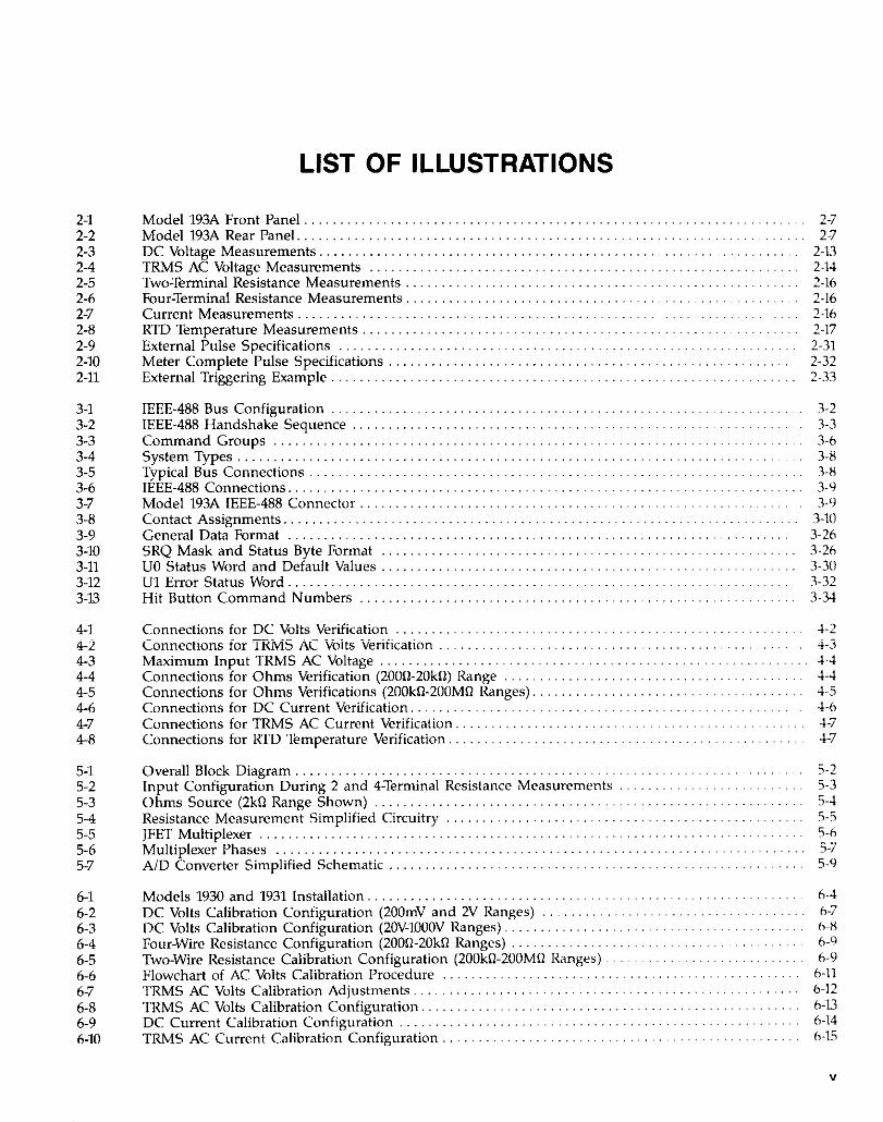
LIST OF ILLUSTRATIONS
2-l 2-2 2-3 2-4 2-5 2-6 2-7 2-8 2-9 Z-10 2-11
3-l 3-2 3-3 3-4 3-5 3-6 3-7 3-8 3-9 3-10 3-11 3-12 3-13
4-l 4-2 4-3 4-4 4-5 4-6 4-7 4-8
Connections for DC Volts Verlflcation .......................................................... 4-2 Connections for TRMS AC Volts Verification ................................................... 4-3 Maximum Input TRMS AC Voltage ............................................................ 4-4 Connections for Ohms Verification (200%20kn) Range .......................................... 4-4 Connections for Ohms Verifications (200k0-200MR Ranges). ..................................... 4-S Connections for DC Current Verification. ...................................................... 4-h Connections for TRMS AC Current Verification ................................................. 1-7 Connections for RTD Temperature Verification. ................................................. -1-7
5-l Overall Block Diagram ............................................... 5-2 Input Configuration During 2 and 4-Terminal Resistance Measurements 5-3 Ohms Source (2k12 Range Shown) .................................... s-4 Resistance Measurement Simplified Circuitry .......................... 5-5 JFET Multiplexer .................................................... 5-6 Multiplexerl’hases ................................................. 5-7 A/D Converter Simplified Schematic ..................................
5.2 5.3 i-4 5-j S-6 j-7 5-9
6-l Models 1930 and 1931 Installation. ........................................................... h-4 6-2 DC Volts Calibration Configuration (2OOmV and 2V Ranges) ..................................... b-7 6-3 DC Volts Calibration Configuration (ZOV-1OOOV Ranges), ......................................... 6-S 6-4 Four-Wire Resistance Configuration (200%20kO Ranges) ......................................... 6-Y 6-5 Two-Wire Resistance Calibration Configuration (200k0-ZOOM0 Ranges). ........................... 6-9 6-6 Flowchart of AC Volts Calibration Procedure .................................................. 6-11 6-7 TRMS AC Volts Calibration Adjustments. ..................................................... 6-12 6-8 TRMS AC Volts Calibration Configuration ..................................................... h-l3 6-9 DC Current Calibration Configuration ........................................................ 6.14 6-10 TRMS AC Current Calibration Configuration .................................................. h-15
Model193A Front Panel ...................................................................... 2-7 Model193ARearPanel ....................................................................... 2-7 DC Voltage Measurements ................................................................... 2.13 TRMS AC Voltage Measurements ............................................................ 2.14 Two-Terminal Resistance Measurements ....................................................... 2-16 Four-Terminal Resistance Measurements. ...................................................... 2-16 Current Measurements.. .................................................................... 2-16 RTD Temperature Measurements.. ........................................................... 2-17 External Pulse Specifications ................................................................ 2-31 Meter Complete Pulse Specifications ......................................................... 2-32 External Triggering Example.. ............................................................... 2-33
IEEE-488 Bus Configuration .............. ...... ...... ...... 3-2 IEEE-488 Handshake Sequence ........... ...... 3-3 Command Groups ...................... ...... ...... 3-6 System Types ........................... ...... ...... 3-8 Typical Bus Connections ................. ...... 3-x IEEE-488 Connections. ................... ...... 3-Y Model 193A IEEE-488 Connector ........ ...... 3-Y Contact Assignments. ................... ...... ...... 3-10 General Data Format ................... ...... ...... ...... 3-26 SRQ Mask and Status Byte Format ..... ...... ...... ...... 3-26 UO Status Word and Default Values ...... ...... ...... ...... 3-30 Ul Error Status Word. .................. ...... ...... 3-32 Hit Button Command Numbers ......... ...... ...... 3-34

6-11 Co”“ectors..................................................... ........................... 6-17 6-12 Model 193A Exploded View. ........................... 6-19
7-1 Jumper Board, Component Location Drawing, Dwg. No. 193.160. 7-2 Display Board, Component Location Drawing, Dwg. No. 193.110 7-3 Display Board, Schematic Diagram, Dwg. No. 193.116 7-4 Digital Board, Component Location Drawing, Dwg. No. 193.100 7-5 Digital Board, Schematic Diagram, Dwg. No. 193-106 7-6 Analog Board, Component Location Drawing, Dwg. No. 193.120 7-7 Analog Board, Schematic Diagram, Dwg. No. 193.126 7-8 Model 1,930, Component Location Drawing, Dwg. No. 1930.100 7-9 Model 1930, Schematic Diagram, Dwg. No. 1930.106 710 Model 1931, Component Location Drawing, Dwg. No. 1931-100 7-11 Model 1931, Schematic Location Drawing, Dwg. No. 1931.106
......
......
...... ...... ...... ...... ...... ...... ...... ...... ......
.............. 7-3
.............. 7-4
.............. 7-5 .............. 7-10 .............. 7-11 ............. 7.22 ............. 7-23 ............. 7.34 ............. 7-35 ............. 7-38 ............. 7-39
vi

LIST OF TABLES
2-l 2-2 2-3 2-4 2-5 2-6 2-7 2-8 2-9
3-l 3-2 3-3 3-4 3-5 3-6 3-7 3-8 3-9 3-10 3-11 3-12 3-n 3-14 3-15 3-16 3-17 3-18
IEEE-488 Bus Command Summary. .......................................................... 3-4 Hexadecimal and Decimal Command Codes ................................................... 3-5 Typical Addressed Command Sequence ...................................... ................ 3-7 Typical Device-Dependent Command Sequence ................................................ 3-7 IEEE Contact Designation .................................................................... 3-9 BASIC Statements Necessary to Send Bus Commands ......................................... 3-11 Model 193A Interface Function Codes ........................................................ 3.11 IEEE Command Groups. .................................................................... 3.12 General Bus Commands and Associated BASIC Statements .................................... 3-12 Factory Default Conditions .................................................................. 3-14 Device-Dependent Command Summary ...................................................... 3-16 Range Command Summary ................................................................. 3-20 High Speed Data Store .................................................................... 2-23 SRQ Command Parameters .................................................................. 3-27 Bus Hold-Off Times ........................................................................ 3-28 Trigger to Reading-Ready Times (DCV Function) .............................................. 3-37 Translator Reserved Words and Character. .................................................... 3-38 Translator Error Messages .................................................................... 3-38
4-l Recommeded Test Equipment .............. 4-2 Limits for DC Volts Verification ............. 4-3 Limits for TRMS AC Volts Verification. ...... 4-4 Limits for Ohms Verification ............... 4-5 Limits for DC Current Verification .......... 4-6 Limits for AC Current Verification .......... 4-7 Limits for RTD Temperature Verification ....
5-l
6-l 6-2 6-3 6-4 6-5 6-6 6-7 6-8 6-9 6-10 6-11 6-12 6-13
Ranging Information ......................................................................... 5.3
Line Voltage Selection ........................................................................ 6-l Line Fuse Replacement ...................................................................... 6-2 Current Fuse Replacement ................................................................... 6-2 Recommended Calibration Equipment ......................................................... DC,Volts Calibratiqn .........................................................................
6;
Resistance Calibration ....................................................................... 6-10 TRMS AC Volts (Model 1930) Calibration ..................................................... 6-13 DC Current Cahbratmn ....................................................................... 6-14 TRMS AC Current Calibration ............................................................... 6-15 Static-Sensltwe Devzes ..................................................................... 6.21 Recommended Troubleshooting Mode ........................................................ Model 193A Troubleshooting Mode ..........................................................
6;:
Power Supply Checks ...................................................................... h-28
Factory Default Conditions ................................................................... 2-l Front PanelPrograms ........................................................................ 2-4 Error and Warning Messages ................................................................. 2-9 Internal Filter ............................................................................... 2.12 Resistance Ranges .......................................................................... 2.15 Corresponding Voltage Reference Levels for Impedance References .............................. 2.19 Comparison of Average and TRMS Meter Readings. ........................................... 2-21 High Speed Data Store ..................................................................... 2.22 Example MX + B Readings ................................................................. Z-28
......
......
......
......
......
......
......
......
......
......
......
vii

6.14 Digital Circuitry Checks ............................................................... 6-28
6-15 Display Circuitry Checks .............................................................. 6-29
7-l Display Board, Parts List .............................................................. 7-2 Digital Board, Parts List .............................................................. 7-3 Analog Board, Parts List,, ............................................................ 7-4 Model 1930, Parts List ................................................................. 7-5 Model 1931, Parts List. ................................................................ 7-6 Model 193A Mechanical Parts List ......................................................
...... 7-2 ...... 7-7
715 7-31 7-37 7-41
vttt

SECTION 1 GENERAL INFORMATION
1.1 INTRODUCTION
The Keithley Model 193A System DMM, with the TRMS AC Volt and Current options installed, is a six function auto- ranging digital multimeter. At 6% digit resolution, the LED display can display ~2,200,OOO counts. The range of this analog-to-digital (A/D) converter is greater than the nor- mal *1,999,999 count AID converter used in many 6% digit DMMs. The built-in IEEE-488 interface makes the instru- ment fully programmable over the IEEE-488 bus. With the TRMS ACV option and the Current option installed, the Model 193A can make the following basic measurements:
1. DC voltage measurements from 1OOnV to lOOOV. 2. Resistance measurements from 1OOpfl to ZOOMR. 3. RTD temperature measurements from -1OOOC to 63O’C. 4. TRMS AC voltage measurements from I$/ to 700V. 5. DC current measurements from 1nA to 2A. 6. TRMS AC current measurements from 1nA to 2A.
In addition to the above mentioned measurement capa- bilities, the Model 193A can make dB and TRMS AC + DC measurements.
1.2 FEATURES
Some important Model 193A features include:
l 14 Character Alphanumeric Display-Easy to read 14 seg- ment LEDs used for readings and front panel messages.
l High Speed Measurement Rate-1000 readings per second.
l Zero-Used to cancel offsets or establish baselines. A zero value can be rogrammed from the front panel or over the IEEE-488 & us.
l Filter-The weighted average digital filter can be set for 1 to 99 readings from the front panel or over the bus.
l Data Store-An internal buffer that can store up to 500 readings is accessible from either the front panel or over the bus.
l Digital Calibration-The instrument may be digitally calibrated from either the front panel or over the bus.
l User Programmable Default Conditions-Any instrument measurement configuration can be established as
the power-up default conditions. l Translator Software-User defined words can be used to
replace standard command strings over the IEEE488 bus. l Thermocouple (TC) temperature measurements con be
made over the IEEE-488 bus.
1.3 WARRANTY INFORMATION
Warranty information may be found on the inside front cover of this manual. Should it become necessary to exer- cise the warranty, contact your Keithley representative or the factory to determine the pmper course of action. Keithley Instruments maintains service facilities in the United States, United Kingdom and throughout Europe. Information concerning the application, operation or ser. vice of your instrument may be directed to the applications engineer at any of these locations. Check the inside front cover for addresses.
1.4 MANUAL ADDENDA
Information concerning improvements or changes to the instrument which occur after the printing of this manual will be found on an addendum sheet included with this manual. Be sure to review these changes before attemp- ting to operate or service the instrument.
1.5 SAFETY SYMBOLS AND TERMS
The following safety symbols and terms are used in this manual or found on the Model 193A.
The A symbol on the instrument denotes that the user should refer to the operating instructions in this manual.
The M on the Instrument denotes that a potential of 1OOW or more may be present on the terminal(s). Stand- ard safety practices should be observed when such dangerous levels are encountered.
The WARNING used in this manual explains dangers that could result in personal injury or death.
The CAUTION used in this manual explains haz.ards that could damage the instrument.
l-l

GENERAL INFORMATION
1.6 SPECIFICATIONS
Detailed Model 193A specifications may be found preceding the Table of Contents of this manual.
1.7 INSPECTION
The Model 193A System DMM was carefully inspected, both electrically and mechanically before shipment. After unpacking all items from the shipping carton, check for any obvious signs of physical damage that may have occurred during transit. Report any damage to the shipping agent. Retain and use the original packing materials in case reship- ment is necessary. The following items are shipped with every Model 193A order:
Model 193A System DMM Model 193A Instruction Manual Additional accessories as ordered.
If an additional instruction manual is required, order the manual package (Keithley Part Number 193-901-00). The manual package includes an instruction manual and any applicable addenda.
1.6 USING THE MODEL 193A MANUAL
This manual contains information necessary for operating and servicing the Model 193A System DMM, TRMS ACV option and the Current option. The information is divided into the following sections:
l Section 1 contains general information about the Model 193A including that necessary to inspect the instrument and get it operating as quickly as possible.
l Section 2 contains detailed operating information on us- ing the front panel controls and programs, making con- nections and basic measuring techniques for each of the available measuring functions.
l Section 3 contains the information necessary to connect the Model 193A to the IEEE-488 bus and program operating modes and functions from a controller.
l Section 4 contains performance verification procedures for the instrument. This information will be helpful if you wish to verify that the instrument is operating in com- pliance with its stated specifications.
l Section 5 contains a description of operating theory. Analog, digital, power supply, and IEEE-488 interface operation is included.
-
1-2
l Section 6 contains information for servicing the instru- ment, This section includes information on fuse replace- ment, line voltage selection, calibration and troubleshooting.
l Section 7 contains replaceable parts information.
1.9 GETTING STARTED
The Model 193A System DMM is a highly sophisticated in- strument with many capabilities. To get the instrument up and running quickly use the following procedure. For com- plete information on operating the Model 193A consult the appropriate section of this manual.
POWW-Up
1. Plug the line cord into the rear panel power jack and plug the other end of the cord into an appropriate, grounded power source. See paragraph 2.2.1 for more complete information.
2. Press in the POWER switch to apply power to the in- strument. The instrument will power up to the 1OOOVDC range.
Making Measurements
1. Connect the supplied safety shrouded test leads to the front panel VOLTS HI and LO input terminals. Make sure the INPUT switch is in the out (FRONT) position.
2. To make a voltage measurement, simply connect the in- put leads to a DC voltage surge (up to 1OOOV) and take the reading from the display.
3. To change to a different measuring function, simply press the desired function button. For example, to measure resistance, press the OHMS button.
Using Data Store
Storing Data: 1. Press the DATA STORE button. The DATA STORE in-
dicator will turn on and a storage rate (in seconds) will be displayed.
2. Select an interval, other than 000.000, using the 4 and w, and data buttons.
3. Press the ENTER button. The buffer size will be displayed. Size 000 indicates that data will overwrite after 500 readings have been stored.
4. If a different buffer size is desired, enter the value us- ing the number buttons (0 through 9).
5. Press the ENTER button to start the storage process.
GENERAL INFORMATION
The data store mode can be exited at any time before the start of the storage process by pressing the RESET button. Once storage has commenced, the storage process can be stopped by pressing any function button. See paragraph 2.7.1 for complete information on storing data.
Recalling Data:
1. Press the RECALL button. The buffer location of last stored reading will be displayed.
2. To read the data at a different manor location, enter the value using the number buttons O-9). Y
3. Press the ENTER button. The reading and the memory location will be displayed.
4. The A and 7 buttons can be used to read the data in all filled memory locations.
5. To read the highest, lowest and average reading stored in the buffer, press the number 1,2 and 3 buttons respec- tively. Note that the memory location of the highest and lowest reading is also displayed. The average reading is displayed along with the number of readings averaged.
The recall mode can be exited by pressing the RESET but- ton. See paragraph 2.7.2 for complete information on data recall.
Using Front Panel Programs
Program selection is accomplished by pressing the PRGM button followed by the button(s) that corresponds to the program number or name. For example, to select Program 91 (IEEE status), press the PRGM button and then 9 and 1 buttons. Table 2-2 lists and briefly describes the available front panel programs. Once a following general rules will P
rogram is selected the app y:
1. A displayed program condition can be entered by press- ing the ENTER button.
2. Program conditions that prompt the user with a flashin digit can be modified usmg the data buttons (0 throug a 9 and +) and the cursor control buttons (manual range buttons).
3. Programs that contain alternate conditions can be dis
K layed by ressin one of the manual range buttons.
Eat press o P P one o these buttons toggles the display between the two available conditions.
4. A program will be executed when the pressed ENTER button causes the instrument to exit the program mode.
5. A pro ram can be exited at an time and thus not ex- ecute 1 , by pressing the RESE if button.
Paragraph 2.8 provides the detailed information for using the front panel programs.
1.10 ACCESSORIES
The following accessories are available to enhance the Model 193As, capabilities.
Model 1301 Temperature Probe-The Model Uol is a rug- ged low cost temperature probe designed to allo\v temper- ature measureme”ts from -55 to 150°C.
Model 16008 High Voltage Probe-The Model 1booB extends DMM measurements to 40kV.
Model 1641 Kelvin Test Lead Set-The Model 1641 has special clip leads that allow 4-terminal measurements to be made while making “nly two c”nnectims.
Model 165150.Ampere Current Shunt-The Model 1651 is an external O.OOlR *l% 4.terminal shunt, which permits current measurements from 0 to 50A AC or DC.
Model 1681 Clip-On Test Lead Set-The Model 1681 con- tains two leads, 1.2m (48’) long terminated with banana plugs and spring action clip probes.
Model 1682A RF Probe-The Model 1682A permits voltage measurements from 1OOkHz to 250MHz. AC to DC transfer accuracy is +ldB from 1OOkHr to 250MHz at IV, peak responding, calibrated in RMS of a sine wave.
Model 1685 Clamp-On AC Probe-The .Model 1685 measures AC current by clamping on to a single conduc- tor. Interruption of the circuit is unnecessary. The Model 1685 detects currents by sensing the changing magnetic field produced by the current flow.
Model 1751 Safety Test Leads-Finger guards and shroud- ed banana plugs help minimize the chance “1 making con- tact with live circuitry.
Model 1754 Universal Test Lead Kit-The Model 1754 is rl 12 piece test lead kit, with interchangeable plug-in ac- cessories. Included in the kit is one set of test leads (l-red, l-black), two spade lugs, two standard banana plugs, two phone tips (0.06 DIA.), two hooks and miniature alligator clips (with boots).
Model 1930 TRMS AC Volt 0 tion-The Model 1930 is d True Root Mean Square (TRM ! ) AC plug-in option for the Model 193A. This option allows the instrument to measure the TRMS value of an AC signal. When the Model 1Y30
1-3

is installed, AC + DC voltage measurements can be made. Field installation or removal/replacement of the Model 1930 will require recalibration of the Model 193A and the Model 1930.
Model 1931 Current 0 current option for the R
tion-The Model 1931 is a plug-in ode1 193A. This option allows the
instrument to measure DC current up to 2A. When both Models 1930 and 1931 are installed, the instrument can make TRMS AC current measurements and TRMS AC + DC current measurements. Field installation requires recalibration of the Model 193A.
Model 1938 Fixed Rack Mount-The Model 1938 is a sta- tionary mount kit that allows the Model 193A to be mounted in a standard 19 inch rack.
Model 1939 Slide Rack Mount-The Model lY39 is a sliding mount kit that allows the Model 193A to be rack mounted with the added feature of sliding the instrument forward for easy access to the rear panel and top cover.
Model 7007 IEEE488 Shielded Cables-The Model 7007 con- nects the Model lY3A to the IEEE-488 bus using shielded cables to reduce electromagnetic interference (EMI). The Model 7007-l is one meter in length and has a EMI shield- ed IEEE-488 connector at each end. The Model 7007-Z is identical to the Model 70071, but is two meters in length.
Model 7008 IEEE-488 Cables-The Model 7008 connects the Model 193A to the IEEE-488 bus. The Model 7008-3 is 0.9m (3 ft.) in length and has a standard IEEE-488 connector at each end. The Model 7008-6 cable is identical to the Model 7008.3, but is 1.8m (6 ft.) in length.
Model 8573 IEEE-488 Interface-The Model 8573 is an IEEE-488 standard interface designed to interface the IBM PC or XT computers to Keithley instrumentation over the IEEE-488 bus. The interface system contains two distinc- tive parts: an interface board containing logic to perform the necessary hardware functions and the handler software (supplied on disk) to perform the required control func- tions. These two important facets of the Model 8573 join together to give the IBM advanced capabilities over IEEE-488 interfaceable instrumentation.
1-4
SECTION 2 BASIC DMM OPERATION
2.1 INTRODUCTION 2.2.2 Power-Up Sequence
Operation of the Model 193A may be divided into two The instrument can be turned on by pressing in the front general categories: front panel operation and IEEE-488 bus panel POWER switch. The switch will be at the inner most operation. This section contains information necessary to use the instrument from the front panel. These functions
position when the instrument is turned on. Upon P
ower- up, the instrument will do a number of tests on itse f. Tests
can also be programmed over the IEEE-488 bus, as describ- are performed on memory (ROM, RAM and NVRAM). If ed in Section 3. RAM or ROM fails, the instrument will lock up. If EYROM
FAILS, the message “UNCALIBRATED” will be displayed. See paragraph 6.92 for a complete description of the pw~er-
2.2 POWER UP PROCEDURE up self test and recommendations to resolve failures.
2.2.1 Line Power 2.2.3 Factory Default Conditions
Use the following procedure to connect the Model 193A to At the factory, the Model 193A is set up so that the front
line power and power up the instrument. panel controls and features are initially configured to cer- tain conditions on power-up and when program RESET is
1. Check that the instrument is set to correspond to the run. These are known as the factory default conditions and
available line oower. When the instrument leaves the fac- are Iisted in Table 2.l,
tory, the internally selected line voltage is marked on the rear panel near the AC power receptacle. Ranges are 105Vl25V or ZloV-250V 50160Hz AC. If the line voltage setting of the instrument needs to be changed, refer to Section 6, paragraph 6.2 for the procedure. If the line frequency setting of the instrument needs to be checked and/or changed, utilize front panel Program 92 (see paragraph 2.8.11) after the instrument completes the power-up sequence.
2. Connect the female end of the power cord to the AC receptacle on the rear panel of the instrument. Connect the other end of the cord to a grounded AC outlet.
Table 2-1. Factory Default Conditions
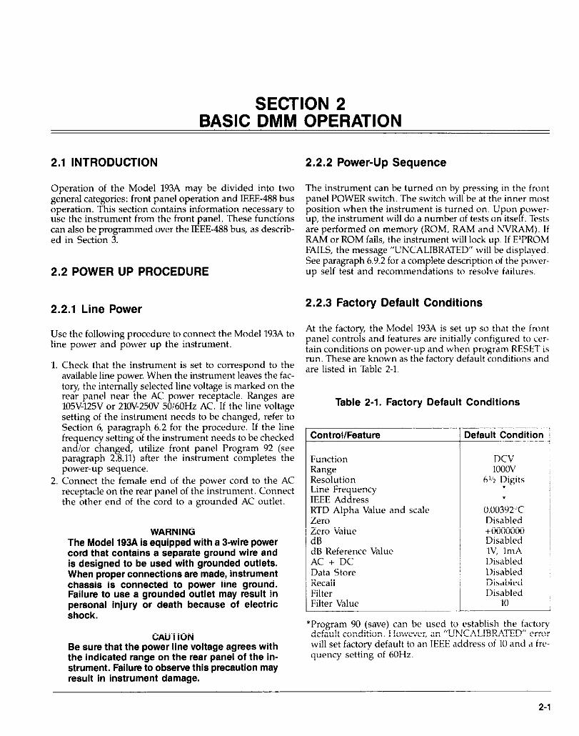
Function Range Resolution Line Frequency IEEE Address RTD Alpha Value and scale ZW” Zero Value dR dB Reference Value AC + DC Data Store Recall Filter Filter Value
WARNING The Model 193A is equipped with a 3-win? power cord that contains a separate ground wire and is designed to be used with grounded outlets. When proper connections are made, instrument chassis is connected to power line ground. Failure to use a grounded outlet may result in personal injury or death because of electric shock.
0.00392LC Disabled +ooooooo Disabled IV, 1mA Disabled Disabled Disabled Disabled
10
CAUTION Be sure that the power line voltage agrees with the indicated range on the rear panel of the in- strument. Failure to ObSSNS this pmCautiOfl may result in instrument damage.
‘Program 90 (save) can be used to establish the factory default condition. However, an “UNCALIBRATED” error will set factory default to an IEEE address of 10 and a ire- quency setting of 60Hz.
DCV 1ooov
6% Digits 1 f
2-1

2.2.4 User Programmed Conditions
A unique feature of the Model 193A is that each function “remembers” the last measurement configuration that it was set up for (such as range, zero value, filter value, etc). Switching back and forth between functions will not affect the unique configuration of each function. However, the instrument will “forget” the configurations on power-down.
Certain confi urations can be saved by utilizing front panel Program 90. % n power-up, these user saved default condi- tions will prevail over the factory default conditions. Also, a DCL or SDC asserted over the IEEE-488 bus will set the instrument to the user saved default conditions. For more information, see paragraph 2.8.9 (Program 90).
NOTE Keep in mind that power-up default conditions can be either factory default conditions or user saved default conditions.
2.3 FRONT PANEL FAMILIARIZATION
The front panel layout of the Model 193A is shown in Figure 2-l. The following paragraphs describe the various com- ponents of the front panel in detail.
2.3.1 Display and Indicators
Display-The 14 character, alphanumeric, LED display is used to display numeric conversion data, range and func- tion mnemonics (i.e. mV) and messages.
Status Indicators-These three indicators apply to instru- ment operation over the IEEE-488 bus. The REMOTE indi- cator shows when the instrument is in the IEEE-488 remote state. The TALK and LISTEN indicators show when the in- strument is in the talk and listen states respectively. See Section 3 for detailed information on operation over the bus.
2.3.2 Controls
All front panel controls, except the POWER and INPUT switches, are momentary contact switches. Indicators are located above certain feature buttons to show that they are enabled. Included are AUTO (autorange), ZERO, FILTER, RECALL and DATA STORE. Some buttons have secondary functions that are associated with front panel program operation. See paragraph 2-8 for detailed Information on front panel programs.
POWER-The POWER switch controls AC power to the in- strument. Depressing and releasing the switch once turns the power on. Depressing and releasing the switch a se- cond time turns the power off. The correct positions for on and off are marked on the front panel by the POWER switch.
INPUT-The INPUT switch connects the instrument to either the front panel input terminals or the rear panel in- put terminals. This switch operates in same manner as the power switch. The front panel input terminals are selected when the switch is in the “out” position and the rear panel input terminals are selected when the switch is in the “in” position.
FUNCTION GROUP-The FUNCTION buttons are used to select the primaly measurement functions of the instru- ment. These buttons also have secondary functions.
DCV-The DCV button places the instrument in the DC volts measurement mode. The secondary function of this button is to enter the number 0. See paragraph 2.6.4 for DCV measurements.
Am-With the ACV option installed, the ACV button places the instrument in the AC volts measurement mode. The secondary function of this button is to enter the number 1. See paragraph 2.6.6 for ACV measurements.
OHMS-The OHMS button places the instrument in the ohms measurement mode. The secondary function of this button is to enter the number 2. See paragraph 2.6.7 for resistance measurements.
ACA-With the ACV option and current option installed, the ACA button places the instrument in the AC amps measurement mode. The secondary function of this but- ton is to enter the number 3. See paragraph 26.8 for ACA measurements.
DCA-With the current option installed, the DCA button places the instrument in the DC amps measurement mode. The secondary function of this button is to enter the number 4. See paragraph 2.6.8 for DCA measurements.
TEMP-The TEMP button places the instrument in the RTD temperature measurement mode. The secondary functions of this button are to select the TEMP program (select alter- nate alpha value and thermometric scale) and to enter the number 5. See paragraph 2.6.9 for RTD temperature measurements.
RANGE GROUP-The Aand vbuttons are used for manual ran ing. These %
ing and the AUTO button is used for autorang- uttons also have secondary functiolw.
2-2

OPERATION
Manual-Each time the A button is pressed, the instru- ment will move up one range, while the v button will move the instrument down one range each time it is pressed. Pressing either of these buttons will cancel autorange, if it was previous selected. The secondary functions of these buttons are associated with front panel program operation.
AUTO-The AUTO button places the instrument in the autorange mode and turns on the AUTO indicator. While in this mode, the instrument will go to the best range to measure the applied signal. Autoranging is available for all functions and ranges. Autoranging may be cancelled by pressin
f the AUTO button or one of the manual range but-
tons. T e secondary function of this button is to enter the * sign.
MODIFIER GROUP-The MODIFIER buttons activate features that are used to enhance the measurement ca bilities of the Model 193A. These features in effect ma Ify 1
a-
the selected function. In addition to their primary tasks, these buttons have secondary functions.
ZERO-The ZERO button turns on the ZERO indicator and causes the displa ed reading to be subtracted from subse- quent readings. -F, his feature allows for zero correction or storage of baseline values. The secondary function of this button is to select the ZERO program. Refer to paragraph 2.6.2 for detailed information on the zero feature.
dB-The dB button places the instrument in the dB measurement mode and may be used with the ACV and ACA functions. Under factory default conditions, measure- ments are referenced to 1V or ImA. However, the dB pro- gram may be used to change the reference level. The secon- dary function of this button is to select the dB program. See paragraph 2.6.10 for dB measurements.
FILTER-The FILTER button turns on the FILTER indicator and causes the instrument to start weighted averaging a number (l-99) of readings. The factory default value is 10, but may be changed using the FILTER program (see paragraph 2.8.6). See paragraph 2.6.3 for filter operation. Selecting the FILTER tions of this button. TK
rogram is one of the secondary func- e other secondary function is to enter
the number 6.
AC + DC-With the appropriate options installed, the AC + DC button (with ACV selected) places the instrument in the AC + DC measurement mode. With the ACV o tion installed, VAC + DC measurements can be made. %ith both the ACV and current option installed, AAC + DC measurements can be made. See paragraph 2.6.12 for AC + DC measurements. The secondary functions of this but- ton are to select the AC + DC program (low frequency TRMS measurements) and to enter the number 7.
CONTROL GROUP-The CONTROL buttons are features that allow for the control and manipulation of various aspects of instrument operation. All of these buttons, ex- cept PRGM, have a secondary function.
RESOLN-The RESOLN button allows for the selection of the number of digits of display resolution. Each press of the RESOLN button increases resolution by one digit. Pressing the RESOLN button after the maximum resolu- tion is reached will revert the display back to the lowest resolution. Dis can be selecte B
lay resolution of 3%, 4’12, 5% or 6% digits for DCV and ACV. Display resolution of
4% or 5’/2 digits can be selected for DCA and ACA. On OHMS, Y/z, 4% 5% and 6% digit resolution is available on the ZOOR through 200kfl ranges. On the 2MQ and 20MR ranges, 5% and 6% digits can be selected. On the 200MR ran e, only 5%d resolution is available. The RESOLN but- ton a as no effect on low frequency AC + DC (Program AC + DC), TEMP or dB measurements. The secondary func- tion of this button is to enter the decimal point (.).
TRIGGER/ENTER-The TRIGGER/ENTER button is used as a terminator for data entry when the instrument is in the front panel program mode and as a front panel trigger when the data store is active.
STATUS/RESET STATUS-Instrument status can be displayed when the in- strument is in the normal measurement mode or logRing readings. When the STATUS button is first pressed, the following current instrument conditions can be displayed with the use of the A and v buttons:
Software revision level IEEE address Line frequency setting Multiplexer status (on/off) MX+B status (on/off) MX+B values dB reference value Filter value (OO=filter disabled) Zero status (on/off) Zero value
Pressing the STATUS button a second time takes the in- strument out of the status mode.
RESET-The RESET button is used to reset the instrument back to the previously entered parameter. Keyed in parameters are only entered after the ENTER button is pressed. If RESET is pressed with the last parameter of a program displayed, the program will be exited and the in- strument will return to the previous operating state. This button aborts back to normal operation when it is in one of the following modes:
2-3

1. The data store is prompting for parameters (interval or size).
2. The instrument is in the RECALL mode. 3. A front panel program has been selected (except Program
AC+DC which is treated as a normal measurement func- tion (see STATUS).
Program RESET-Program RESET returns the instrument to the factory default conditions. See paragraph 2.8.7 for information on using this program.
DATA STORE-The DATA STORE button selects the 500 point data store mode of operation. Paragraph 2.7 contains a complete description of data store operation. The secon- dary function of this button is to enter the number 9.
RECALL-The RECALL button recalls and displays readings stored in the data store. Paragraph 2.7.2 provides a detailed procedure for recalling data. The secondary func- tion of this button is to enter the number 8.
I’RGM-The PRGM button places the instrument in the front panel program mode. Table 2-2 lists the available pro- grams. Paragraph 2.8 contains descriptions and detailed operating procedures for each front panel program.
2.3.3 Input Terminals
The input terminals are intended to be used with safety shrouded test leads to help minimize the possibility of con- tact with live circuits. Note that the terminals are duplicated on the rear panel and that the INPUT switch determines which set of terminals is active.
VOLTS OHMS HI and LO-The VOLTS OHMS HI and LO terminals are used for making DC volts, AC volts and two- wire resistance measurements.
AMPS and LO-The AMPS and LO terminals are used for making DC current and AC current measurements.
OHMS SENSE HI and LO-The OHMS SENSE HI and LO terminals are used with the VOLTS OHMS HI and Lx) ter- minals to make four-wire resistance measurements and four-wire RTD temperature measurements.
2.3.4 Current Fuse
The current fuse protects the Model 1931 from input cur- rent overloads. The instrument can handle UD to 2A con-
LOCAL-When the instrument is in the IEEE-488 remote tinuously or 2.2A for less than one minute. l&fer to para-
state (REMmE indicator on), the LOCAL button will return graph 6.3.2 for the current fuse replacement procedures.
the instrument to front panel operation. However, if local lockout (LLO) was asserted over the IEEE-488 bus, the LOCAL button will be inoperative. See Section 3 for infor- 2.4 REAR PANEL FAMILIARIZATION mation on operating the instrument over the IEEE-488 bus.
The rear panel of the Model 193A is shown in Figure 2-2.
Table 2-2. Front Panel Programs
TEMP AC+DC
dB ZERO FILTER
RESET
4 90 91 92
93 94 95 96
L
Set RTD value and scale. Low Frequency TRMS AC + DC. Recall/modify dB reference value. Recall/modify zero value. Recall/modify number of readings aver- aged (filter value). Reset internal conditions to factorv default.
i
MX + B select. save current front panel setup. Recall/modify IEEE address. Recall/modify line frequency setting (50160Hz). Self-test Set values for MX + B program Multiplexer on/off. Digital calibration.
2.4.1 Connectors and Terminals
AC Receptacle-Power is applied through the supplied power cord to the 3-terminal AC receptacle. Note that the selected supply voltage is marked on the rear panel near the connector.
Input Terminals-The rear panel input terminals perform the same functions as the front panel input terminals. Paragraph 2.3.3 contains the description of the input terminals.
IEEE-488 Connector-This connector is used to connect the instrument to the IEEE-488 bus. IEEE interface functions are marked above the connector.
External Trigger Input-This BNC connector is used to ap- ply pulses to trigger the Model 193A to take one or more readings, depending on the selected trigger mode.
2-4

OPERATION
Voltmeter Complete Output-This BNC output connector input. Refer to paragraph 6.3.1 for the tine fuse replacement provides a pulse when the Model 193A has completed a procedure. reading. It is useful for triggering other instrumentation.
2.4.2 Calibration Switch 2.5 ERROR AND WARNING DISPLAY
MESSAGES
Calibration of the Model 193A can only be done if the calibration switch is in the unlock position.
Table 2-3 lists and explains the various display messages associated with incorrect front panel operation of the Model 193A. Also included is a warning message that indicates
2.4.3. Line Fuse to the user that hazardous voltages (4OV or more) are pre- sent on the input terminals.
‘The line fuse provides protection for the AC power line
2-512-6


OPERATION
CONTROL
0
Figure 2-1. Model 193A Front Panel
Figure 2-2. Model 193A Rear Panel
2-112-8


OPERATION
Table 2-3. Error and Warning Messages set to voltage range if the minimum voltage spacing is reduced.
I(
.....-“J’ -..y.“..“.*-..
NEED 1930 Selected option not installed. NEED 1931
NEED 1930.1931 “H” High Voltage: 4OV or more on
input. NO PROGRAM Invalid entry while trying to
select program. 1.VERFLO KOHM Overrange-Decimal point position
and mnemonics define function and range (Zkfl range shown). The number of characters in the “OVERFLO” message defines the display resolution (6%d resolu- tion shown).
TRIG-OVERRUN Trigger received while still pro- cessmg reading from last trigger.
CONFLICT Trying to calibrate with instru- ment in an improper state.
<OT ACV or ACA Selecting AC+DC or dB with in- strument not presently in ACV or ACA.
SHORT-PERIOD Instrument, as currently con- figured, cannot run fast enough to store readings at the selected interval.
2.6 BASIC MEASUREMENTS
When making measurements in high energy circuits use test leads that meet the following requirements:
l Test leads should be fully insulated. l Only use test leads that can be connected to the circuit
(e.g. alligator clips, spade lugs, etc.) for hands-off measurements.
l Do not use test leads that decrease voltage spacing. This diminishes arc protection and creates a hazardous condition.
Use the following sequence when testing power circuits:
1. De-energize the circuit using the regular installed connect-disconnect device such as the circuit breaker, main switch, etc.
2. Attach the test leads to the circuit under test. Use ap- propriate safety rated leads for this application.
3. Set the DMM to the proper function and range. 4. Energize the circuit using the installed conncct-
disconnect device and make measurements without disconnecting the DMM.
5. De-energize the circuit using the installed connect- disconnect device.
6. Disconnect the test leads from the circuit under lest.
WARNING The following paragraphs describe the basic procedures for making voltage, resistance, current, temperature, dB, and
The maximum common-mode input voltage
AC + DC measurements. An ACV option must be install- (the voltage between input LO and chassis
ed for ACV measurements, the current option must be in- ground) Is 500V peak. Exceeding this value may create a shock hazard.
stalled for DCA measurements and both options must be installed for ACA and AAC + DC measurements.
2.6.1 Warm Up Period
High Energy Circuit Safety Precautions
To optimize safety when measuring voltage in high energy distribution circuits, read and use the directions in the following warning.
WARNING Dangerous arcs of an explosive nature in a high energy circuit can cause severe personal injury or death. If the meter is connected to a high energy circuit when set to a current range, low resistance range or any other low impedance range, the circuit is virtually shorted. Danger- ous arcing can result even when the meter is
The Model 193A is usable immediately when it is first turn- ed on. However, the instrument must be allowed to warm up for at least one hour to achieve rated accuracy.
2.6.2 Zero
The zero feature sewes as a means of baseline suppression by allowing a stored offset value to be subtracted from subsequent readings. When the ZERO button is
R rewed,
the instrument takes the currently displayed rea mg as a baseline value. All subsequent readings represent the dif- ferences between the applied signal level and the stored baseline.
2-9

OPERATION
A baseline level can be established for any or all measure- ment functions and is remembered by each function. For example, a XIV baseline can be established on DCV, a 5V baseline can be established on ACV and a 1OkQ baseline can be established on OHMS. These levels will not be cancelled by switchin back and forth between functions. Once a baseline is esta hshed for a measurement function, %, that stored level will be the same regardless of what range the Model 193A is on. For example, if 1V is established as the baseline on the 2V range, then the baseline will also be 1V on the 2OV through 1OOOV ranges. A zero baseline level can be as large as full range.
NOTE The following discussion on dynamic range is based on a display resolution of 6% digits. At 5% digit resolution, the number of counts would be reduced by a factor of 10. At 4%d resolution, counts would be reduced by a factor of 100 and 3%d reso- lution would reduce counts by a factor of 1000.
By design, the dynamic measurement range of the Model 193A, at 6% digit resolution, is 4400000 counts (excluding the 1OOOVDC and 700VAC ran es). With zero disabled, the
% displayed reading range of t e mstrument is +2200000 counts. With zero enabled, the Model 193A has the capabili- ty to display &IO0000 counts. This increased display range ensures that the dynamic measurement range of the instru- ment is not reduced when using a zero baseline value. The following two exam les will use the maximum allowable zero values (+2200 00 counts and -2200000 counts) to CT show that dynamic measurement range will not be re- duced. It is important to note that the increased display range does not increase the maximum allowable input level to the instrument. For example, on the 2V range, the Model 193A will always overrange when more than +2.2V is con- nected to the input.
Example l-The instrument is set to the 2VDC range and a maximum -2.2OOOOOV is established as the zero value. When -2.2OOOOOV is connected to the in ut of the Model 193A. the disolav will read O.OOOOOOV. &en +2.2ooooov is connected &I tGe input, the display will read +4.4OOOOOV. Thus, the dynamic measurement range of the Model 193A is OV to 4.4V, which is 4400000 counts.
Example Z-The instrument is still set to the 2VDC range, but a maximum +2.2OOOOOV is the zero level. When +2.2OOOOOV is connected to the input of the Model 193A, the display will read O.OOOOOOV. When -2.2OOOOOV is con- nected to the input, the display will read -4.4COOOOV. Thus the d
9 to 0 namic measurement range of the instrument is -4.4V
, which is still 4400000 counts.
Zen, Correction-The Model 193A must be properly zeroed when using the 2OOmV DC or the 2003 range in order to achieve rated accuracy specifications. To use ZERO for zero correction, perform the following steps:
1. Disable zero, if button. The Z IT
resently enabled, by pressing the ZERO RO indicator will turn off.
2. Select the 2OOmV DC or the 2000 range. 3. Connect the test leads to the input of the Model 193A
and short them together. If four-wire resistance measurements are to be made, connect and short all four leads together.
Note: At 5% and 6% digit resolution, low measurement techniques need to be employed. Use Kelvin test leads or shielded test leads. See paragraph 2.6.5 for low level measurement considerations.
4. Press the ZERO button. The display will read zero. 5. Remove the short and connect the test leads to the signal
or resistance to be measured.
Note: Test lead resistance is also compensated for when zeroing the 2000 range with the above procedure.
Baseline Levels-Baseline values can be established by either applying baseline levels to the instrument or by set- ting baseline values with the front panel ZERO program. Paragraph 2.8.5 contains the complete procedure for using the ZERO program. To establish a baseline level by apply- ing a level to the Model 193A, perform the following steps:
1. Disable zero, if presently enabled, by pressing the ZERO button. The ZERO indicator will turn off.
2. Select a function and range that is appropriate for the anticipated measurement.
3. Connect the desired baseline level to the in Model 193A and note that level on the P
ut of the disp ay.
4. Press the ZERO button. The display will zero and the ZERO indicator will be enabled. The previously displayed reading will be the stored baseline. The zero baseline value will also be stored in Program ZERO, replacing the previous zero value.
WARNING If *4OV or more is present on the input ter- minals, the Model 193A will display the mnemonic “H” to indicate the presence of hazardous voltage. For example, the display “OO.OOOOHVDC” indicates than k4OV or more is present on the input.
5. Disconnect the stored signal from the input and connect the signal to be measured in its place. Subsequent readings will be the difference between the stored value and the applied signal.
2-10
Notes:
Disabling zero cancels the zero baseline value on that selected function. However, since the zero value is auto- matically stored in Program ZERO, the zero baseline value can be retrieved by using the program as long as the ZERO button is not again pressed (see paragraph 2.8.5 for details). Pressing the ZERO button, thus enabl- ing zero, will wipe out the previous baseline value in Pro- 3 gram ZERO. Baselines established on other functions are not affected.
OPERATION
filter indicator light will blink for three time constants. A time constant is measured in readings. The number of readings in one time constant is equal to the fitter value. For example, for a filter value if 10, one time con- stant is equal to 10 readings and three time constants would be equal to 30 readin bc shorter in the 3%d mo 3
s. The blinking duration will e since that has the fastest
reading rate. In a continuous trigger mode, a reading that is clutsidc the filter window will cause the fitter indicator to blink for one time constant.
To store a new baseline on a selected function, zero must first be disabled and then enabled again. The new value will be stored with the first triggered conversion. The Digital Filter-The Model 193A utilizes a digital filter to ‘It- baseline value will also be stored as the zero value in tenuate excess noise present on input signals. The filter is Program ZERO, cancelling the previously stored value. a weighted average type. The mathematical representation Setting the range lower than the suppressed value will is: overrange the display; the instrument will display the overrange message under these conditions. (new reading -AVG(t-I))
When the ZERO button is pressed to enable zero, the A”G(t) = ,,“G(t-1) + ~~~~~~~ ~~~ ~~
zero indicator light will blink until an on scale reading F
is available to use as a zero level.
Where,
2.6.3 Filter AVG(t) = displayed average
When the filter is enabled, a number of measurements are AVG(t-1) = old displayed average
averaged before being displayed. The factory default F = weighting factor (filter value)
number is 10, but it can be changed to a value from 1 to 99 with the use of the FILTER program. A filter value can be set for any or all measurement functions and is remem-
As with any filter, the Model 193A digital fitter \\.ilt affect
bered by each function. For example, a filter value of 20 can reading response time. The step response for this filter ib
be set for DCV and a filter value of 55 can be set for ACV. of the form:
These filter values will not be cancelled by switching back and forth between functions.
step response = l-K’“*”
An advantage of using the filter is to stabilize the reading Where,
of a noisy input level. A consideration of filter usage is that the larger the number of readings averaged, the longer the
“K” is a constant based on the filter weighting factor
response time of the display. Perform the following pro- cedure to use the filter:
1 K=l-
1. If it is desired to check and/or change the filter value, 0 7
utilize Program FILTER as explained in paragraph 2.8.6. 2. Press the FILTER button. The FILTER indicator will turn
“n” is the reading number.
On.
The step occurs when n=O. n=l is the first wading ,Ifter
Notes: the step, n=2 is the second reading, etc.
1. Pressing the FILTER button a second time will disable Therefore: the filter.
2. After a reading is triggered (continuous or one-shot), the “t/
step response = 1
2-11

Example:
F = 10 n=5
= ,468
Five readings after the step occurs, the display will be at =47% of the step change. After 10 readings (n=lO), the dis- play will be at = 68% and after 20 readings, the display will be at -88%. The more the readings, the closer the display will be to the step change.
To speed the response to large step changes, the Model 193A digital filter employs a “window” around the dis- played average. As long as new readings are within this window, the displayed value is based on the weighted average equation. If a new reading is outside of this win- dow, the displayed value will be the new reading, and weighted averaging will start from this point. The step response was one reading to this change. The window in the Model 193A filter is 10,000 counts for 6%d resolution, 1000 counts for 5%, 100 counts for 4X and 10 counts for 3Y2.
Internal Exponential Filter-In addition to the front panel digital filter, an internal exponential digital filter is used when making high resolution and high sensitivity measure- ments. Like the front panel digital filter, it is a weighted average type. The enable/disable status of the filter is con- trolled over the IEEE bus. However, under factory default conditions, the instrument powers up with the filter enabled. When enabled, exponential filtering only occurs when the instrument is in the 5% or 6’/2 digit resolution mode. Table 2-4 summarizes this filter.
Notes:
1. The front panel FILTER indicator light does not turn on when the internal filter is activated. The indicator is only used with the front oanel digital filter.
2. Internal filtering does not occur on ranges and functions not listed in Table 24.
3. Controlling the internal filter (on/off) over the IEEE bus is explained in paragraph 3.10.23.
4. In a one-shot trigger mode, the Model 193A will not out- put a reading until both digital filters have settled. Three time constants are used to allow the filters to settle. A time constant is measured in readings. The number of readings in one time constant is equal to the filter value. For example, for a filter value of 10, three time constants would be equal to 30 readings. If both the internal filter and the front panel filter are in use, the time constant is the sum of both filter values.
5. Filter windows for the internal filter function in the same manner as the windows for the front panel filter. How- ever, the window sizes of the internal filter are much smaller than the front panel filter window sizes.
2.6.4 DC Voltage Measurements
The Model 193A can be used to make DC voltage measure- ments in the range of +lOOnV to +lOOOV. Use the follow- ing procedure to make DC voltage measurements.
1. Select the DC volts function by pressing the DCV button. 2. Select a range consistent with the expected voltage or use
autorange. 3. Select the front or rear panel input terminals with the
INPUT switch.
Table 2-4. internal Filter
c 5VzDieit Resolution I 6% Dieit Resolution
Range/Function
Internal Filter Value
Internal Filter
Window Range/Function Value
200mVDC 5 6 digits 200mVDC 35 2.1000VDC 10
ZOO-200kn 5 6 digits 200-200k0 40 2MO, 20MO 10 40 digits 2MO, 20MR 40
All DCA 5 6 digits All ACV 10
Window
60 digits 20 digits
60 digits 400 digits
20 digits
2-12

OPERATION
NOTE The 2OOmV DC range requires zero to be set in order to achieve rated accuracy. The zero correction procedure can be found in paragraph 2.6.2.
4. Connect the signal to be measured to the xlectcd input terminals as shown in Figure 2-3.
5. Take the reading from the display.
2.6.5 Low-Level Measurement Considerations
Accuracy Considerations-For sensitive measurements, other external considerations besides the Model 193A will affect the accuracy. Effects not noticeable when working with higher voltages are significant in nanovolt and microvolt signals. The Model 193A reads only the signal received at its input; therefore, it is important that this signal be properly transmitted from the source. The follow- ing paragraphs indicate factors which affect accuracy, noise, source resistance, thermal emfs and stray pick-up.
Noise and Source Resistance-The limit of sensitivity in measuring voltages with the Model 193A is determined by the noise present. The displayed noise is inherent in the instrument and is present in all measurements. The noise voltage at the Model 193A input increases with source resistance.
For high impedance sources, the generated noise can become significant when using the most sensitive range (ZOOmV, 6%d) of the Model 193A. As an example of deter- mining e. (noise voltage generation due to Johnson noise of the source resistance), assume that the Model 193A is connected to a voltage source with an internal resistance of lM0. At a room temperature of 2O”C, the p-p noise voltaee eenerated over a bandwidth of 1Hz will be:
Thus, an e, of 0.635pV would be displayed at h%d resolu- tion as an additional 6 digits of noise on the Model 193A. To compensate for the displayed noise, use digital filtering and then zero out the settled offset.
Shielding-AC voltages which are extremely large com- pared with the DC signal may erroneously produce a DC. output. Therefore, if there is AC interference, the cirruit should be shielded with the shield connected to the Model 193A input W (particularly for low-level sources). Improper shielding can cause the Model 193A to beh,we in one or more of the following ways:
1. Unexpected offset voltages. 2. Inconsistent readings between ranges 3. Sudden shifts in reading.
To minimize pick-up, keep the voltage wurw and the Model 193A away from strong AC magnetic swrccs. .I’he voltage induced due to magnetic flux is proportional to the area of the loop formed by the input leads. Therefore. minimize the loop area of the input leads and connect each signal at only one point.
Thermal EMFs-Thermal emfs (thermoelectric potentials) are generated by thermal differences between the junction of dissimilar metals. These can be large compared to the signal which the Model 193A can mcawre. Therm.tl emfs can cause the following problems:
1. Instability or zero offset is much higher than expected. 2. The reading is sensitive to (and responds to) temperature
changes. This can be demonstrated by touching the cir- cuit, by placing a heat source near the circuit or by a regular pattern of instability (corresponding to heatmg and air-conditioning systems or changes in sunlight).
3. To minimize the drift caused by thermal emfs, use cop- oer leads to connect the circuit to the Model 193. A v ”
e, = 6.35 x 10.‘O JR x f &~ana plug is generally suitable and generates just a few microvolts. A clean copper conductor such as ~10
e, = 6.35 x 10-l” J(1 x i0’) (1) bus wire is about the best for this application. The leads
e. = 0.635rV to the input may be shielded or unshielded, as necessary Refer to Shielding.
Figure 2-3. DC Voltage Measurements
2-13

4. Widely varying temperatures within the circuit can also create thermal emfs. Therefore, maintain constant temp- eratures to minimize these thermal en&. A cardboard box around the circuit under test also helps by minimiz- ing air currents.
5. The ZERO control can be used to null out constant offset voltages.
2.6.6 TRMS AC Voltage Measurements
With the ACV option installed, the instrument can make TRMS AC voltage measurements from 1pV to 7OOV. To measure AC volts, proceed as follows:
1. Select the AC volts function by pressing the ACV button. 2. Select a range consistent with the expected voltage or use
autorange. 3. Select the front or rear panel input terminals using the
INPUT switch.
NOTE There is a small amount of offset (typically 150 counts at 5%d) present when using the ACV func- tion. Do not zero this level out. Paragraph 2.6.13 provides an explanation of AC voltage offset.
4. Connect the signal to be measured to the selected input terminals as shown in Figure 2-4.
5. Take the reading from the display.
Crest Factor-Rated accuracy to 3 at full scale for pulse widths >lO~sec and peak voltage <1.5 x full scale. For crest factors >3 but ~10, typical accuracy is degraded ac- cording to the following calculation:
AD = (CF-3) x 0.36%
Where: AD is accuracy degradation CF is the crest factor
Also, the peak signal must be less than 5 x full scale, but not more than the maximum input specification.
Notes:
1. See paragraph 2.6.13 for TRMS measurement considera- tions.
2. For TRMS AC+DC measurements, see paragraph 2.6.12. 3. To make low frequency AC measurements in the range
of 1OHz to 20Hz: A. The ACV option must be installed. B. The ACV function must be selected. C. Digital filtering must be used to obtain a stable
reading. D. Allow enough settling time before taking the reading.
4. To make low frequency voltage measurements in the range of O.lHz to lOHz, use Program AC+DC (see paragraph 2.8.3). The ACV option does not have to be installed for these measurements.
Clarifications of Model 1930 TRMS ACV Specifications:
Settling Time-0.5sec to within 0.1% of change in reading. This time specification is for analog circuitry to settle and does not include A/D conversion time.
NOTE When making TRMS AC voltage measurements below 45Hz (ACV function selected), enable the front panel filter modifier to obtain stable readings. A filter value of 10 is recommended.
I I . c--
AC VOLTAGE ------.
I - - - - - - - - _ - - - - - - SOURCE . .
MODEL 193A
CA”T,ON: MAXIMUM INPUT lOO0” PEAK AC / DC, 2 x lO’V.Hr ,NP”T ,MPEDANCE = 1 MI1 SHUNTED BY < 120pF
Figure 2-4. TRMS AC Voltage Measurements
2-14

OPERATION
Table 2-5. Resistance Ranges
6%d Range I Resolution
200 0 2 kR
20 kR 200 k!7
2MO 20MO
200MR
O.lIdl 1mR
1omn 1OOmQ A 10 10 0
100 R
I current Through Unknown
1mA ImA
100 PA 10 WA 1 +A
100 nA 100 “A*
*Short circuit current only.
Maximum Test Lead Resistance (Q) for
<l Count Error (6Vzd)
312 10 32 100 320 lk
2.6.7 Resistance Measurements
The Model 193A can make resistance measurements from lOO@ to 200MQ. The Model 193A provides automatic selec- tion of 2.terminal or 4.terminal resistance measurements. This means that if the ohms sense leads are not connected, the measurement is done 2.terminal. If the sense leads are connected, the measurement is done 4-terminal. For 4. terminal measurements, rated accuracy can be obtained as long as the maximum lead resistance does not exceed the values listed in Table 2-5. For best results on the 2000, 2kQ and 20kQ ranges, it is recommended that 4.terminal measurements be made to eliminate errors caused by the voltage drop across the test leads which will occur when 2. terminal measurements are made. The Model 1641 Kelvin ‘Test Lead Set is ideal for low resistance 4-terminal measure- ments. To make resistance measurements, proceed as follows:
1. Select the ohms function by pressing the OHMS button. 2. Select a range consistent with the expected resistance or
use autorange. 3. Select the front or rear panel input terminals using the
INPUT switch.
NOTE The 2OOn range requires zero to be set in order to achieve rated accuracy. The zero correction pro- cedure can be found in paragraph 2.6.2.
4. For 2-terminal measurements connect the resistance to
the instrument as shown in Figure 2-S. For 4.terminal measurements connect the resistance to the instrument as shown in Figure 2-6.
CAUTION The maximum input voltage between the HI and LO Input terminals is 350V peak or 250V RMS. Do not exceed these values or instrument damage may occur.
5. Take the reading from the display.
Notes:
1. Incorrect readings will result if the resistance being measured is part of a live circuit.
2. Table 2-5 shows the current output for each resistance range.
3. It hel s to shield resistance greater than 1OOkR to achieve a sta le reading. Place the resistance in a shielded & enclosure and electrically connect the shield to the LO input terminal of the instrument.
4. Diode Test-The 2kR range can be used to test diodes as follows: A. Select the 2kR range. B. Forward bias the diode by connecting the red terminal
of the Model 193A to negative side of the diode. A good diode will typically measure between 5000 to 242.
C. Reverse bias the diode by reversing the connections on the diode. A good diode will olwrange the display.
2-15
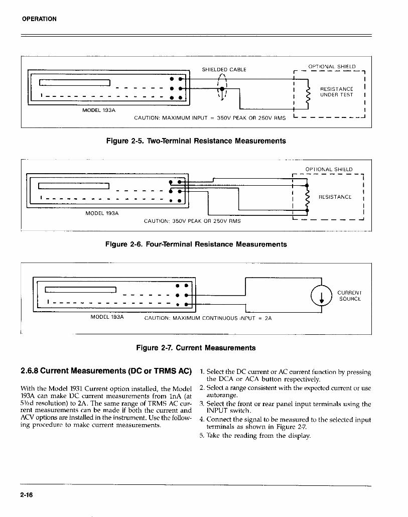
OPERATION
I 1 SHIELDED CABLE OPTIONAL SHlELD r. I--- -------I
I I 1
. . ,, , I I ------ l I-1
L I - - - - - - - - - - - - _ - _ . . \ !
MODEL 193A L
I RESISTANCE 1
I UNDER TEST ,
I I I
CAUTION: MAXIMUM INPUT = 350” PEAK OR 250” RMS L--------J
Figure 2-5. Two-Terminal Resistance Measurements
OFTONAL SHlELD r--------i
I I
RESISTANCE , I
Figure 2-6. Four-Terminal Resistance Measurements
I I . .
---me-* CURRENT
I - - - - - - - - - - - - - - - . SOURCE
MODEL 193% CAUTION: MAXlMUM CcmTlN”clLE ,NPVT = 2A
Figure 2-7. Current Measurements
2.6.6 Current Measurements (DC or TRMS AC) 1. Select the DC current or AC current function by pressing the DCA or ACA button respectively.
With the Model 1931 Current option installed, the Model 2. Select a range consistent with the expected current or use 193A can make DC current measurements from 1nA (at autorange. 5%d resolution) to 2A. The same range of TRMS AC cur- rent measurements can be made if both the current and
3. Select the front or rear panel input terminals using the INPUT switch.
ACV options are installed in the instrument. Use the follow- ing procedure to make current measurements.
4. Connect the signal to be measured to the selected input terminals as shown in Figure 2-7.
5. Take the reading from the display.
216

OPERATION
Figure 2-8. RTD Temperature Measurements
2.6.9 RTD Temperature Measurements
The Model 193A can make temperature measurements from -100” to +63O”C (-148’ to +llOOOF) using platinum RTD sensors. Resolution is 0.01 “C or “F. The front panel TEMP program allows the user to select the alternate alpha value (0.00385 or 0.00392) and the alternate thermometric scale (“C or “F). See paragraph 2.8.2 for detailed information for using the TEMl’ program. Use the following procedure to make RTD temperature measurements.
1. Select the RTD temperature function by pressing the TEMI’ button.
2. The instrument will now display one of the following readings:
OVERFL “C PRTD or OVERFL “F PRTD
The display is overranged at this time because an RTD sensor is not yet connected to the input. The “F or “C indicates the current thermometric scale and PRTD indi- cates the measurement mode (platinum resistance tem- perature device),
3. To check and/or change the alpha value or thermometric scale, utilize the TEMP program (see paragraph 2.8.2).
4. Select the front or rear panel input terminals with the INPUT switch and connect the platinum RTD sensor to the instrument as shown in Figure 2-8.
5. Take the reading from the display.
NOTE With additional instrumentation, the Model 193A has the capability of making temperature measure- ments using thermocouple (TC) sensors. Selection of the various TC modes can only be accomplished over the IEEE-488 bus. See paragraph 3.1022 for more information.
2.6.10 dB Measurements
The dB measurement mode makes it possible to compress a large range of measurements into a much smaller scope. AC dB measurements can be made with the instrument in the ACV or ACA function. The relationship between dB and voltage and current, can be expressed by the follow ing equations:
I<” dB = 20 log ~
0 1 W,
At the factory the instrument is set up to be a dBV meter when ACV dB is selected. dBV is defined as decibels above or below a 1V reference. The instrument will read OdB when 1V is applied to the input. The 1V reference is the factor\ default reference and is indicated on the display by the “\p’ mnemonic. Thus, whenever “dBV” is displayed. the operator will know that the reference is IV. Uith ACA dB selected, the factory default reference is 1mA. The instru- ment will read OdB when 1mA is applied to the input.
Reference levels other than 1V and lmA can be established. There are two methods that can be used to establish a dB reference. One method is to use the zero feature. This simp- ly consists of applying a signal to the instrument and press- ing the ZERO button. That suppressed level is the dB reference (OdB point). The alternate method is to utilize the front panel dB program and enter the desired reference value. An advantage of using the dB program is that a source is not needed to establish a reference.
2-17
OPERATION
The following procedure explains how to use the zero feature to establish a reference:
1. Apply a voltage or current signal, that is to be used as the dB reference, to the input of the Model 193A.
2. Press the ZERO button. The ZERO indicator will turn on and the display will zero. The reference is now whatever the applied signal is.
3. Disconnect the signal from the instrument.
Program dB allows the the user to check or change the dB reference of the instrument. The recommended program- mable voltage reference range is from 1OpV to 9.99999V. The recommended programmable current reference range is from 1OnA to 9.99999mA. Paragraph 2.8.4 contains the in- formation needed for using the dB program.
AC dB Measurements-Perform the following steps to make dB measurements:
1. Select the ACV or ACA function. 2. Select the front or rear panel input terminals with the
INPUT switch. 3. Check and/or change the dB reference as previously
explained. 4. Connect the signal to be measured to the input of the
Model 193A. 5. if AC + DC dB measurements are to be made, press the
AC + DC button.
Note: DC dB measurements can be made by selecting the AC + DC modifier as long as there is no AC compo- nent present on the input signal.
6. Enable the dB measurement mode by pressing the dB button.
7. Take the dB reading from the display.
WARNING If 40V or more is present on the input terminals, the Model 193A will display the the mnemonic “H” to indicate the wesence of hazardous voltage. For example, the display “60.00 dBV H” indicates that 40V or more is present on the input.
The following information explains the displayed mnemonics that are associated with dB measurements:
dBV = dB voltage measurement mode with the dB reference at 1v. dB = dB voltage measurement mode. dBA = dB current measurement mode. Unlike dBV, this message does not define the dB reference. dBV A+D = AC+DC dB voltage measurement mode with 1v reference. dB A+D = AC+DC dB voltage measurements. dBA A+D = AC+DC dB current measurement mode. H = High Voltage: 40V or more on input. This mnemonic could be displayed with any of the above messages.
dBm Measurements-dBm is defined as decibels above or below a 1mW reference. dB measurements can be made in terms of impedance rather than voltage or current. Because the instrument cannot directly establish impedance references, a voltage reference must be calculated and established for a particular impedance reference. Use the following equation to calculate the voltage reference need- ed for a particular impedance reference:
For OdBm, V,,f = &IW l Z,,f
Example: Calculate the voltage reference needed to make dBm measurements referenced to 6OOa.
For OdBm, V,,f = Jti.OOlW . 600R = J.6 = J.T7T56\1
Once the necessary voltage reference is known, it can be established in the Model 193A with the dB program. Subse- quent dBm readings will be referenced to the correspon- ding impedance reference. Table 2-6 lists the voltage references needed for some commonly used impedance references.
dBW Measurements-dBW is defined as decibels above or below a 1W reference. dBW measurements are made in the same manner as dBm measurements; that is, calculate the voltage reference for a particular impedance and set the in- strument to it with the dB program. The only difference between dBm and dBW is the reference point; 1mW vs 1W. The following equation can be used to calculate the voltage reference:
For OdBW, V,,f = JIW*Zref
2-16
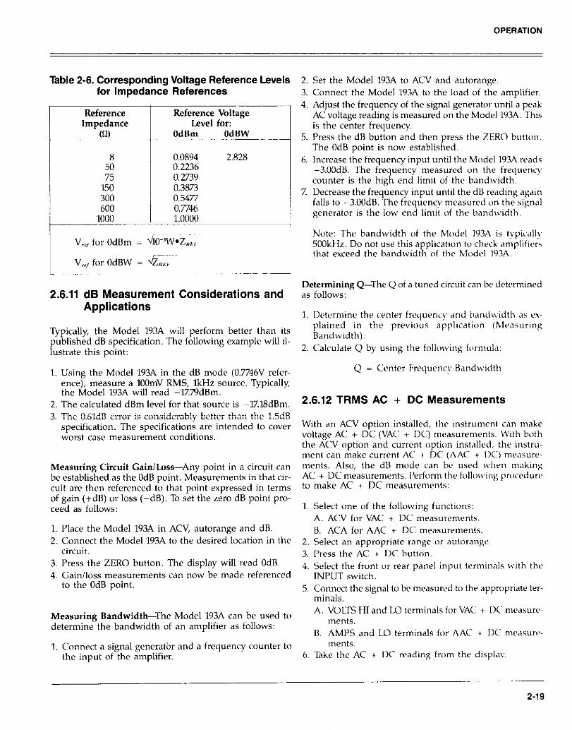
OPERATION
Table 2-6. Corresoondina Voltaae Reference Levels 2. Set the Model 193A to ACV and autoranrre. II
for Imbedance References
Reference Reference Voltage Impedance Level for:
m OdBm OdBW
8 50 75
0.0894 2.828 0.2236
150 300 600
1000
0.2739 0.3873 0.5477 0.7746 1.0000
V,, for OdBm = viO~‘W*Z,,,~
V,, for OdBW = k,,,
2.6.11 cfB Measurement Considerations and Applications
3. Connect the Model 193A t” the load “f the amplifier. 4. Adjust the frequency of the signal generator until a peak
AC voltage reading is measured “n the Model 193A. This is the center frequency.
5. Press the dB button and then press the ZERO button The OdB point is now established.
6. Increase the frequency input until the Model 193A reads -3.OOdB. The frequency measured on the frequent! counter is the high end limit of the bandwidth.
7. Decrease the frequency input until the dB reading again falls to -3.OOdB. The frequency measured “n the signal generator is the low end limit “f the band\vidth.
Note: The bandwidth of the Model 193A is typic.lll! 5OOkHz. Do not use this a plication to check amplifiers that exceed the T bandwidt I of the Model 193A.
Determining Q-The Q of a tuned circuit can be determined as f01l0ws:
1. Dctcrmine the center frequency and handwidth as ex-
Typically, the Model 193A will perform better than its plained in the previous applxatwn (Measuring
published dB specification. The following example will il- Bandwidth).
lustrate this point: 2. Calculate Q by using the following formula:
1. Usinz the Model 193A in the dB mode (0.7746V refer- Q = Center Frcquenc~,Band\~idth
ace! measure a 1OOmV RMS, lkHz source. Typically, the Model 193A will read -17.79dBm.
2. The calculated dBm level for that s”urce is -17.18dBm. 2.6.12 TRMS AC + DC Measurements
3. The 0.61dB error is considerably better than the 1.5dB specification. The specifications are intended to c”ver worst case measurement conditions.
Measuring Circuit Gain/Loss-Any point in a circuit can be established as the OdB point. Measurements in that cir- cuit are then referenced to that point expressed in terms of gain (+dB) or loss (-dB). To set the zero dB point pro- ceed as follows:
1. Place the Model 193A in ACV, autorange and dB. 2. Connect the Model 193A to the desired location in the
With an ACV option installed, the instrument can make voltage AC + DC (VAC + DC) measurements. With both the ACV option and current option installed, the instru- ment can make current AC + DC (AAC -t. UC) meaure- men&. Also, the dB mode can bc used !chen making AC + DC measurements. Perform the following pr”ax~urc to make AC + DC measurements:
1. Select one of the following functions: A. ACV for VAC + DC measurements. B. ACA for AAC + DC measurements.
2. Select an appropriate range or autorange circuit. 3. Press the AC + DC button.
3. Press the ZERO button. The display will read OdB. 4. Gain/loss measurements can now be made referenced
4. Select the front or rear panel input terminals with the INPUT switch.
to the OdB point. 5. Connect the signal to be measured t” the appropriate ter- minals.
Measuring Bandwidth-The Model 193A can be used to A. VOLTS HI and LO terminals for VAC + DC mcdsuw
determine the bandwidth of an amplifier as follows: merits.
B. AMPS and LO terminals for AK t DC rnexurtl-
1. Connect a signal generatbr and a frequency counter t” merits.
the input of the amplifier. 6. Take the AC + DC reading from the display.
2-19

Perform the following procedure to make dB AC + DC measurements.
1. Select one of the following functions: A. ACV for VAC + DC measurements. 8. ACA for AAC + DC measurements.
2. Select autoranging for optimum resolution. 3. Select the front or rear panel input terminals using the
INPUT switch. 4. Press the AC + DC button. 5. Check and/or change the dB reference of the instrument
as explained in paragraph 2.6.10. 6. Connect the signal to be measured to the instrument. 7. Press the dB button and take the reading from the
display.
The following information explains the displayed mnemonics that are associated with measurements:
VA+D = AC+DC voltage measurement mode. AA+D = AC+DC current measurement mode. dBV A+D = AC+DC dB voltage measurement mode with 1v reference. dB A+D = ACcDC dB voltage measurement mode. dBA A+D = AC+DC dB current measurement mode. LO VA+D = Low frequency AC+DC voltage measurement mode (Program AC+DC). H = High Voltage: 40V or more on input. This mnemonic could be displayed with any of the dB measurements.
Notes:
1. To make low frequency AC + DC measurements in the range of 1OHz to 20Hz: A. An ACV option must be installed. B. The ACV function must be installed. C. Digital Filtering must be applied, D. Allow enough settling time before taking the reading.
2. To make low frequency AC + DC voltage measurements in the range of O.lHz to lOHz, use Pro (see paragraph 28.3). An ACV option f
ram AC + DC oes not have to
be installed for these measurements.
2.6.13 TRMS Considerations
Most DMMs actually measure the average value of an in- put waveform but are calibrated to read its RMS equivalent. This poses no problems as long as the waveform being measured is a pure, low-distortion sine wave. For complex, nonsinusodial waveforms, however, measurements made
with an averaging type meter can be grossly inaccurate. Because of its TRMS measuring capabilities, the Model 193A (with an ACV option installed) provides accurate AC measurements for a wide variety of AC input waveforms.
TRMS Measurement Comparison-The RMS value of a pure sine wave is equal to 0.707 times its peak value. The average value of such a waveform is 0.637 times the peak value. Thus, for an average-responding meter, a correction factor must be designed in. This correction factor, K can be found by dividing the RMS valued by the average value as follows:
K = 0.70710.637 = 1.11
By applying this correction factor to an averaged reading, a typical meter can be designed to give the RMS equivalent. This works fine as long as the waveform is a pure sine, but the ratios between the RMS and average vaues of different waveforms is far from constant, and can vary considerably.
Table 2-7 shows a comparison of common types of waveforms. For reference, the first waveform is an ordinary sine wave with a peak amplitude of 1OV. The average value of the voltage is 6.3W, while its RMS value is 7.07V If we apply the 1.11 correction factor to the average reading, it can be seen that both meters will give the same reading, resulting is no error in the average-type meter reading.
The situation changes with the half-wave rectified sine wave. As before, the peak value of the waveform is IOV, but the average value drops to 3.18V. The RMS value of this waveform is 5.OOV, but the average responding me- ter will give a reading of 3.53V (3.18 x 1.11), creating an error of 29.4%.
A similar situation exists for the rectified square wave, which has an average value of 5V and an RMS value of 5.0~ The average responding meter gives a TRMS reading of 5.55V (5 x Ill), while the Model 193A gives a TRMS reading of 5V. Other waveform comparisons can be found in Table 2.7.
AC Voltage Offset--The Model 193A, at Wzd resolution, will typically display 150 counts of offset on AC volts with the input shorted. This offset is caused by amplifier noise and offset of the TRMS converter. This offset will not affect reading accuracy and should not be zeroed out using the zero feature. The following equation expresses how this off- set (Voffset) is added to the signal input (Vi,,):
2-20

OPERATION
Displayed reading = d (V,.)’ + (V,8,.,)’
Example: Range = WAC Offset = 150 counts (1.5mV) Input = 2OOmV RMS
Display reading = mF+~ (1151%~
= JO.04V + (2.25 x WV) = .200005V
The offset is seen as the last digit which is not displayed at 5% digit resolution. Therefore, the offset is negligible. If the zero feature was used to zero the display, the 150 counts of offset would be subtracted from Vi, resulting in an error of 150 counts in the displayed reading.
Crest Factor-The crest factor of a waveform is the ratio of its peak value to its RMS value. Thus, the crest factor specifies the dynamic range of a TRMS instrument. Far sinusoidal waveforms, the crest is 1.414. Far a symmetrical square wave, the crest factor is unity.
The crest factor of other waveforms will, of course, depend on the waveform in question because the ratio of peak to RMS value will vary. For example, the crest factor of a rec- tangular pulse is related to its duty cycle; as the duty cycle decreases, the crest factor increases. The Model lY3A has a maximum crest factor of 3, which means the instrument will give accurate TRMS measurements of rectangulx waveforms with duty cycles 11s low as 10?~~.
Table 2-7. Comparison of Average and TRMS Meter Readings
Sine +10--
'I
%
rialf-Wave Rectified Sine
+b”-
Full-Wave Rectified Sine
jquare +10- -
0 %-
iectified Square Wave
““Cl--
rriangular Sawtooth
kc Coupled Peak
Value
1ov
IOV
1OV
IOV
1ov
1OV
IOV
RMS VdlIe
7.07v
5.oOV
7.07v
1o.ctlv
5.oov
ov ‘fi
5.77v
*wage Responding
bleter Readim
7.07v
3.533
7.07v
ll.lOV
5.55v
*l.lV-ll
5.55v
29.4%
0%
11%
!.llYY-l)x 102%
2-21

OPERATION
2.7 DATA STORE Readings will be stored as fast as the instrument can run.
Data Store can store up to 500 readings, plus the minimum, maximum and average reading. Data can be stored at a user selectable rate.The rates span from lmsec to 16.67 minutes (999.999s~). Manual triggering is available (one-shot mode). In this mode, one reading is stored every time the TRIGGER button is pressed. Also, while in the one shot- mode, an external trigger source can be used to control the fill rate of the data store.
High Speed Data Store-The data store must be utilized to take advantage of the high speed measurement capabilities of the Model 193A. With the data store set at its fastest storage rate (1000 readings per second), up to a half second burst of data (500 readings) can be stored. The stored readin the IE #a
s can be retrieved from the front panel or sent over E-488 bus.
The data store is considered to be in the high speed mode, whenever one of the four fastest intervals (lmsec, Zmsec, 3msec and 4msec) is selected. In the high speed mode, the data store will only operate if the instrument is in a valid state. Table 2-8 lists the operating states that the instrument must be in to achieve high speed data storage. If the con- ditions in the table are not met when attempting to start the storage process, the instrument will exit the data store mode and return to the previous operating state.
NOTE: At 5%d and 6%d resolution, the fastest valid storage interval is 4Omsec. An interval less than 40msec will result in a short period error when the storage process is started.
2.7.1 Storing Data
Perform the following procedure to store data:
1. Press the DATA STORE button. The current storage interval (in seconds) will be displayed. An interval of 000.000 indicates that the one-shot mode is selected.
2. If a storage interval other than the one displayed is desired, enter the desired interval as follows: Cursor location is indicated by the bright flashing digit. Number entry is accomplished by placing the cursor on the character to be modified and pressing the appropriate data button (buttons numbered 0 through 9). Cursor control is provided by the 4 and) buttons which move the cursor left and right respectively. If the cursor is mov- ed past the least significant digit, it will move back to the most significant digit.
3. With the desired storage interval displayed, press the ENTER button. A message that defines the size of the data store (up to 500 memory locations) will then be displayed. The size number determines how many readings will be stored before the storage cycle stops. However, the size number 000 indicates that the storage cycle will continue even after 500 readings have been stored. After the 500th reading is stored, readings will be stored beginning at the first memory location over- writing the previously stored data. Example: The follow- ing message will be displayed if the current size of the data store is 100:
END = 100
Table 2-0. High Speed Data Store
I I Valid Functions
DCV, ACV, DCA, ACA, AC+DC (except low frequency
AC+DC)
Valid Ranges Valid Reading Rates
3%d All, except Autorange 3%d
4%d
1
*Data store sire 000 (continuous) cannot be used in the high speed data store mode.
2.22

OPERATION
Note that the data store indicator light will blink while waiting for the trigger. A
B,
C
If a storage interval other than 000.000 is selected, press the TRIGGER button.
Readings will then start storing at the selected inter- val. The storage process is indicated by the flashing DATA STORE indicator li (remains on) when the 3
ht. The light stops flashing ata store is full.
NOTE: If a high speed interval is selected (lms, 2ms, 3ms or 4ms), the display will blank for a short period of time while the readings are being stored. If the in- strument is in an invalid o speed data storage (see Table 5
crating state for high -8), the instrument will
exit the data store mode. If storage is to be done manually (one-shot mode 000.000 interval selected), press the TRIGGER button.
Each press of the TRIGGER button will display and store one reading in the data store. The DKCA STORE indicator light will continue to flash until the defin- ed buffer size is filled. After the buffer fills, the light will remain on. If the storage rate is to be controlled by an external trigger source (one-shot mode OOO.COO interval
4. If it is desired to change the size of the data store, enter the size value. The procedure to enter data is explained in step 2. If an attempt is made to enter a data store size greater than 500, the size will default to 500.
NOTE: Up to this point, pressing the RESET button will disable the data store and return to the previous state of operation.
5. With the desired data store size value displayed, press the ENTER button. The following message will be displayed briefly:
ENTERED
A prompt, indicating that the instrument is waiting for a trigger to start the storage process will then be displayed. For example, with the instrument on the 1OOWDC range, at 6%d resolution, the following prompt will be displayed:
----,~-- V,,C
selected), connect the trigger source to the EXTER- NAL TRIGGER INPUT connector on the rear panel of the instrument (see paragraph 2.10.1 for trigger pulse specifications), and press the TRIGGER button.
Each subse to be store 2
uent trigger pulse will cause rl reading
Notes: Whenever numeric data entry is prompted for (storage interval and buffer size), the decimal oint button (‘V’) will clear the display to all zeroes. ‘&is is especially useful when s&&g the data store one-shoi mod; (000.000). When storing readings with AUTO range enabled, the dis
K lay will autorange as usual, but recalled readings \cill
re ect the range that the instrument was on when the data store was enabled. Once data storage has started, the data store can he disabled by pressing any function button. That function will then be selected. However, if RECALL is also en- abled, the data store can only be disabled by pressing the RESET button first and then a function button. The front panel message “SHORT-PERIOD” indicates that the instrument, as currently configured, cannot run fast enough to store readings at the selected interval. For example, the instrument cannot store readings ‘lt a selected interval of 1Omsec if the unit is in the 53 rate mode (16.7msec integration period). In this case, the in- strument will only store as fast as it can run. Enabling the data store does not clear the buffer of previously stored readings. Instead, new readings \vill overwrite old readings starting at buffer location 001.
2.7.2 Recalling Data
Stored data may be recalled any time during or after the storage process as follows:
1. Press the RECALL button. The RECALL indicator will turn on and the memory location of the last stored reading will be displayed. For example, if the last stored reading was in memory location 20, then the following message will be displayed:
LQc=o20
2-23

OPERATION
2. If it is desired to read the data in the dislayed memory location, then proceed to step 3. If it is desired to read the data at a different memory location, then the displayed memory location number must be changed as follows: Cursor location is indicated by the bright, flashing digit. Number entry is accomplished b plac- ing the cursor on the character to be modified an 2 press- ing the appropriate data button (buttons numbered 0 through 9). Cursor control is provided by the 4 and ) buttons which move the cursor left and right respectively. If the cursor is moved pass the least significant digit, it will move back to the most significant digit.
3. With the desired memory location number displayed, press the ENTER button. The following message will be displayed briefly:
ENTERED
Entering a number that is greater than the defined data store size, will default the display to the highest memory location defined by the data store size.
4. The stored data will then be displayed along with the memory location. For example, if 193,OOOOV is stored at memory location 20, then the following message will be displayed:
193.0000 020
5. To read the stored data from all filled memory locations, utilize the manual range buttons. The A button in- crements the memory location number and displays the data stored there. After the highest filled memory loca- tion is read, the A button continues the reading pro- cess at memory location 001. Conversely, the v button decrements the memor the data stored there. A Y
location number and displays ter memory location 001 is read,
the v button continues the reading process at the highest filed memory location.
6. To read the highest, lowest and average reading stored in the data store, proceed as follows: A. To display the highest reading, enter the number 1
by pressing the “1” button. The following message will be displayed briefly:
HI=
The highest stored reading along with the memory location of that reading will be displayed.
B. To display the lowest reading stored, enter the number 2 by pressing the “2” button. The following message will be displayed briefly:
LO=
The lowest stored reading along with the memory location of that reading will be displayed.
C. To display the average reading, enter the number 3 by pressing the “3” button. The following message will be displayed briefly:
AVE=
The average reading along with the number of memory locations used to calculate the average will be displayed. Memory locations that have an over- range reading will not be included in the average.
NOTE With a HI, Lo or AVE reading displayed, pressing the AUTO button will return the display to the last normal recalled reading. The A button performs the same function as the AUTO button, except that it increments the displa tion. Conversely, the P
to the next memory loca- button decrements the
memory location.
In the recall mode, the status of the Model 193A, while it was storing readings, can be checked by pressing the “0” button. The function that the instrument was in will be displayed. For example, if storage was performed in the DC volts mode, the following message will be displayed when the “0” button is pressed:
VDC Use the A and v buttons to display the rest of the status messages which include: IEEE address Frequency setting Multiplexer status (on/off) MX+B status (on/off) M value B value dB reference value Filter value Zero status (on/off) Zero value To exit the status mode, press the STATUS button. To exit the recall mode, press the RESET button.
Notes:
1. If the data store is enabled and full while in the recall mode, DATA STORE indicator light will be on, but not flashing.
2. Low, high and average readings will continue to be up- dated as long as readings are still being stored in the data store.
3. After the instrument is turned off, readings in the data store will be retained for typically up to five days.

4. Enabling the data store does not clear the buffer of pre- viously stored readings. Instead, new readings will over- write old readings starting at buffer location 001.
2.8 FRONT PANEL PROGRAMS
There are fourteen programs available from the front panel of the Model 193A. These programs are listed in Table 2-2. The following paragraphs describe and explain the opera- tion of each program.
2.8.1 Cursor and Data Entry
Many of the Model 193A programs need data to be applied from the front panel. After these programs are selected, cursor location is indicated by a bright, flashing display digit with the rest of the modifiable characters at normal brightness.
Data entry is accomplished by placing the cursor on the appropriate character to be modified and pressing the selected data button (0 through 9, or decimal point). Cur- sor control is provided by the RANGE 4 and ) buttons which move the cursor left and right respectively. If the cur- sor is moved pass the least significant digit, it will move back to the most significant digit. Polarity (+ button) can be changed with the cursor on any character. Plus (+) is implied and thus, not displayed. When entering data, the decimal point button (‘“‘) can be used to clear the display to read all zeroes.
2.8.2 Program TEMP
Program TEMP allows the user to select the alternate RTD alpha value (0.00385 or 0.00392) and change the thermo- metric scale (“C or “F). Pam mph 2.6.9 provides informa-
&I tion necessary for making R temperature measurements. Perform the following steps to use this program:
1. Press the PRGM button. The following prompt will be displayed:
PROGRAM 7
2. Press the TEMP button. The current alpha value will then be displayed. If the instrument is currently set to the fac- tory default alpha value, the following message will be displayed:
RTD a = 0.00392
3. Pressing one of the range buttons will toggle the display to the alternate alpha value as shown:
RTD a = 0.00385
4. To enter the displayed alpha value, press the ESTER huts ton. The following message will be displayed brietly:
ENTERED
5. The current thermometric scale will then be displayed. If the instrument is currently on “C, the follwving message will be displayed.
6. Pressing one of the range buttons \\.ill tog& the diz+>~ to the alternate scale as shorvn:
7. To enter the displayed scale, press the ENTER button. The following message will be displayed briefly and the instrument will return to the previous operatmg state.
ENTERED
Note: Alpha value 0.00392 and ‘C are the factory default power-up conditions. If it is desired to have the alternate alpha value and/or “F on dition(s) using Program T
ower-up, select the alternate con- EMP followed by 1’rr)g:r.m~ ‘JO to
save it (see paragraph 2.8.9).
2.8.3 Program AC + DC (Low Frequency AC)
Program AC + DC configures the Model lY3A to make lo!\ frequency (0.1 to 10H.z) TRMS AC + DC voltage measurements at 3%d resolution. Keep in mind that the ACV option does not have to bc installed for these measurements. Perform the following steps to USE this program:
1. Press the PRGM button. The following prompt will be-displayed:
PROGRAM?
2. Press the fiC+DC button The displayed reading will be accompamed by the mnemomc ’ LO VA+D”.
3. Select a range that is appropriate for the anticipated measurement. It is recommended that AUTC range not be used.
4. Connect the signal to be measured to the input of the Model 193A.
2-25

OPERATION
5. The instrument will then start displaying readings that will ramp to the final TRMS value.
NOTES:
1. The final reading will be achieved in approximately 3 to 4 minutes. This long time constant is due to the low fre- quency cutoff of O.lHz.
2. It does not matter what function the instrument is in when this program is selected.
3. To exit the program, press any function button.
2.8.4 Program dB
Program dB allows the user to check and/or modify the dB reference. The programmable voltage reference can be up to 9.99999V and the programmable current reference can be up to 9.999991~4. Detailed information on dB measure- ments is provided in paragraphs 2.6.10 and 2.6.11. Perform the following steps to use this program:
1. Press the I’RGM button. The following prompt will be displayed:
PROGRAM ?
2. Press the dB button. The current reference level will be displayed. Example: If the reference is 1V or lmA, the following message will be displayed:
REF = 1.00000
3. Modify, if desired, the dB reference level as explained in paragraph 2.8.1 Cursor and Data Entry, and press the ENTER button. The recommended reference range is lo@ to 9.99999V and 1OnA to 9.99999mA. The following message will be displayed briefly and then the instru- ment will return to the previously defined state.
ENTERED
Note: The factory default power-up voltage reference is l.OOOOOV with the instrument in ACV and l.OOOOOmA with ACA selected. If it is desired to have a different voltage reference on power-u
7, 5 modif the voltage
reference using Program dB fol owed by rogram 90 to save it (see paragraph 2.8.9).
2.8.5 Program ZERO
Program ZERO allows the user to check or modify the zero value. A complete explanation of the zero modifier can be found in paragraph 2.6.2. Once a zero value is set on a
measurement function, that zero level is the same on all the ranges. For example: If 1V DC is set as the zero value on the 2V DC range, the zero value in the program will be displayed as 1.000000. On the 20V DC range the zero value will still be 1V DC, but will be expressed as 01.00000 in the program.
Perform the following procedure to implement Program ZERO.
1. Press the PRGM button. The following prompt will be displayed:
PROGRAM 7
2. Press the ZERO button. The current zero value will then be displayed. Example: If the instrument is on the 20V DC range and the current zero value is +3V DC, the following message will be displayed:
z = 03.00000
3. If it is desired to retain the displayed zero value, press the ENTER button. The instrument will return to the previous operating state with the zero modifier en- abled. The displayed reading will reflect the entered zero value.
4. To modify the zero value, do so as explained in paragraph 2.8.1, Cursor and Data Entry, and press the ENTER button. The instrument will return to the previously defined state with the zero modifier enabled using the newly entered zero value.
Note: The factory default power-up zero value is 0000.000. If it is desired to have a different zero value displayed on power-up, modify the zero value using Pro- gram ZERO followed by Program 90 to save it (see paragraph 2.8.9).
2.8.8 Program FILTER
Program FILTER allows the user to modify the weighting of the exponential filter. Valid filter values are from 1 to 99. More information concerning the filter can be found in paragraph 2.6.3.
Perform the following steps to check and/or modify the filter value:
1. Select the desired function. 2. Press the PRGM button. The following prompt will be
displayed:
PROGRAM ?
2-26

OPERATION
Press the FILTER button. The current filter value will then be displayed. Example: If the filter value is 5, the following message will be displayed:
FILTER = 05
If it is desired to retain the displayed filter value, pro- ceed to step 5. If it is desired to modify the filter v&c, do so as explained in paragraph 2.8.1 Cursor and Data Entry. With the desired filter value displayed, press the ENTER button. The following message will be displayed briefly and the instrument will return to the previously defined state with the filter enabled.
ENTERED
To check or change the filter value of another function, select the function and repeat steps 2 through 5.
1. Program RESET can be aborted by pressing any front panel momentary button, except the ENTER button, when the prompt “PRESS ENTER” is displayed. The instrument will return to the previous operating state.
2. Once the instrument is reset to the factory default con- ditions with this program, Program 90 must be run if it is desired to have the factory default conditions on subsequent power-ups.
2.8.8 Program 4
This program allows the operator tu automatically multipl! normal display readings (X) by a constant (M) and add a
Program 94 (see paragraph 2.8.~13). Perform the folkwing
constant (8). The result (Y) will be displayed in accordance
steps to enable the MX + B feature:
with the formula, Y =MX + B. This program is useful when slope calculations are required for a series of mc‘.xure- mats. The values of M and B can be changed by utilizing
Notes:
1. The factory default power-up filter value is 10. If it is desired to have a different filter value on power-up, change the filter value using Program FILTER followed by Program 90 to save it (see paragraph 2.8.9).
2. Entering a filter value of 00 will default the filter value back to the previous value and return the instrument to the previously defined state with the filter disabled.
Set the Model 193A to the desired function and range. Connect the signal to be measured (X) to the input of the Model 193.A If the values of M and B need to be checked or chang- ed, do so using Program 94. Press the PRGM button. The folknving prompt will be displayed:
2.8.7 Program RESET I’ROGRAM ?
Program RESET resets all instrument setup parameters back to factory default conditions. The factory default con- ditions are listed in Table 2-l. Perform the following steps to run this program:
5 Enter the number 4 b rent status of the M 2%
ressing the “4” button The cur- + program will be displayed. For
example, if the MX+B iscurrently disabled, the follow- ing message will bedisplayed:
1. Press the PRGM button. The following prompt will be displayed.
MX+B OFF
6
PROGRAM ?
Any range button will toggle the display to the alter- nate MX + B status. Thus, press a range button and the following message will be displayed:
2. Press the RESET button. The following message will be displayed briefly:
PROGRAM RESET
MX+B ON
7
3. The following prompt will then be displayed:
With the message “MX+B ON” displayed, press the ENTER button to enable MX + B. The folknving message will be displayed briefly and the instrument tvill return to the function initially set.
PRESS ENTER ENTERED
4. Press the ENTER button. The following message will be displayed briefly and the instrument will return to the factory default conditions.
8 All subsequent readings (Y) will be the result of the equation: Y = MX + B.
ENTERED
2-27

OPERATION
Notes: Other instrument parameters, that are saved include:
1. The MX + B feature can be disabled by again running RTD alpha value Program 4. While in the program, press a range button until the message “MX+B OFF” is displayed and then
Temperature scale (“C/OF)
press the ENTER button. dB reference
2. Once MX + B has been enabled, the Model 193A will MX+B status (on/off)
show the value of Y. If the value of Y is larger than can MX+B “alues
be handled by the particular range, the overrange IEEE Primary address message will be displayed, indicating the instrument Line frequency setting must be switched to a higher range. Multiplexer status (on/off)
3. An exam& of readinas that will be obtained when MXfB is ‘enabled is shown in Table 2-9. Each of the ob- tained values for Y assumes the following constants: M Perform the following procedure to use the save program: = +1.5; B = +5.
Table 2-9. Example MX + B Readings
1. Set up the instrument as desired or run Program RESET (see paragraph 2.8.7) to return the instrument to the fac- tory default conditions.
2. Press the PRGM button. The following prompt will be
193A Range and Function
MX + B* Reading 0’)
1 displayed:
PROGRAM ?
2WDC 20VDC 2WAC 20kQ
8.OOOOOVDC -5.OOOOOVDC 6.3OOOOVAC
“Where M = +1.5 and B = +5.
2.8.9 Program 90 (Save)
17.0000WDC -2.5000WDC 14.45OOWAC ll.OOOOOk0
3. Enter the number 90 by pressin the “9” and “0” but- tons. The following message WI 1 be dlsplayed briefly: ,B
PROGRAM SAVE
4. The following message will then be displayed:
PRESS ENTER
5. To save the instrument setup conditions, press the ENTER button. The following message will be displayed
Program 90 saves current instrument conditions set up by the user. These user programmed conditions will then replace the previously saved default conditions on ower- up. Also, an SDC or DCL asserted over the IEEE- B 88 bus will return the instrument to these saved conditions.
briefly:
ENTERED
6. The instrument will return to the conditions set up in step 1 and will now power-up to those conditions.
One function (including dB, AC+DC or low frequency AC+DC) may be saved along with the following para- meters:
Range Resolution Zero status (on/off) and value Filter status (on/off) and value
On the other functions, filter and zero values are the only parameters that are be saved.
Notes:
1. To exit the program without changing the previous default conditions, press any front panel button except the ENTER button. The instrument will return to the operating states set up in step 1.
2. To return the instrument to the factory power-up default conditions, use Program Reset (see paragraph 2.8.7) and save the conditions using Program 90.
3. When using this program, make sure that the rest of the instrument is in the desired operating state.
2-28

OPERATION
2.8.10 Program 91 (IEEE Address)
Program 91 allows the user to check and/or modify the ad- dress of the IEEE-488 interface. The interface can be set to any rimary address from 0 to 30. Detailed information on the EEE-488 bus is provided in Section 3. Perform the P following steps to use this program:
:I. Press the PRGM button. The following prompt will be displayed:
PROGRAM ?
2. Enter the number 91 by pressing the “9” and “I” but- tons. The IEEE address value will be displayed. Exam- ple: If the current primary address of the instrument is 10, the following message will be displayed:
IEEE=10
3. If it is desired to retain the displayed status value, pro- ceed to step 4. To change the status value, enter the ad- dress number (0 to 30) as explained in paragraph 2.8.1.
4. With a valid status value displayed, press the ENTER but- ton, the following message will be displayed briefly and the instrument will return to the previously defined state.
ENTERED
Notes:
1. If an in&id number is entered, the instrument will exit from the program with the IEEE primary address being set to 30.
2. To change the factory power-up default address of the instrument, select the desired IEEE address using this program and then Program 90 to save it.
2.8.11 Program 92 (Freq)
The Model 193A does not automatically detect the power line frequency upon power-up. This program allows the user to check the line frequency settin of the instrument and to select the alternate frequency. f he mstrument can be set to either 50Hz or 60Hz. Perform the following steps to check and/or change the line frequency setting of the Model 193A:
1. Press the PRGM button. The following prompt will be displayed:
PROGRAM ?
2. Enter the number 92 by pressing the “Y and “2” buttons. The current line frequency setting will then be displayed. If the instrument is currently set to hOHz, the following message will be displayed:
FREQ= 60HZ
3. If the displayed frequency setting matches the available line frequency, proceed to step 4. If the alternate line tre- quency setting is needed, press one of the manual range buttons. The display will toggle to the alternate frequent\ setting as shown:
FREQ = 50Hz
4. With the correct frequency setting displfyed, press the ENTER button. The following message ~111 bc d~splaved briefly and the instrument will return to the previous operating state.
ENTERED
Note: To change the factory power-up frequency setting of the instrument, select the alternate frequency setting using this program and then run Program 90 to save it.
2.8.12 Program 93 (Diagnostics)
Program 93 is a diagnostic program designed to switch on various switching FET’s, relays and logic levels to allow si nal tracing through the instrument. Refer to paragraph 6. 8 .3 in the maintenance section to use this program to troubleshoot the instrument.
2.8.13 Program 94 (MX + B Status)
This program allows the operator to check/change the M and B values for the MX + B feature (Program 4) of the Model 193A. The factory power-up default value of M is 1.000000 and the value of B is 0000000. See paragraph 2.8.8 for complete information on the MX + B feature. To check/change the values of M and B, proceed as follows:
Press the PRGM button. The following prompt will be displayed:
PROGRAM ?
Enter the number 94 by pressin the “9” and “4” but- tons. The current value of M WI now be displayed. If .& the factory default value is the current value of M, then the following message will be displayed:
M= 1.000000
2-29

If it is desired to retain the displayed M value, proceed to step 4. If it is desired to modify the M value, do so as explained in paragraph 2.8.1 Cursor and Data Enhy Note that valid M values are in the range of -9.999999 to +9.999999. With a M value displayed, press the ENTER button. The following message will be displayed briefly:
ENTERED
The current B value will now be displayed. If the factory default value is the current B value, the following message will be displayed:
B= 0000.000
Decimal point position is determined by the ran e that the instrument was on when this program was se B ected.
If it is desired to retain the displayed B value, proceed to step 7. If it is desired to modify the value of M, do so as explained in paragraph 2.8.1 Cursor and Data Engi Note that the B value range is from 0.0001x10-’ to +9999.999. With a valid B value displayed, press the ENTER button. The following message will be displayed briefly and the instrument will return to the previously defied state of operation.
ENTERED
Notes:
1. User selected values of M and B will be stored within the Model 193A until the power is turned off (unless saved bv Prorram 90). These constants will be used whenevir Mf+B is enabled. Note, however, that the value of B is scaled according to the range in use. Exam- ple: A value of 19.00000 entered for B is actually 19.OOOOOV with the instrument on the 20V range and lYO.OOOOV with the instrument on the 2OO.OOOOV range.
2. The user can set the values for M and B as the power-up default values by running Program 90 (see paragraph 28.9).
2.8.14 Program 95 (Multiplexer)
The multiplexer auto zeroical routines may be defeated by running Program 95. Using the Model lY3A with the auto zeroical defeated increases measurement speed and is useful for making high impedance DC voltage measure- ments which can be affected by the input multiplexing. Per-
form the following steps to run this program:
1. Press the PRGM button. The following prompt will be displayed:
PROGRAM ?
2. Enter the number 95 by pressing the “9” and “5” buttons. The current multiplexer status will then be displayed. For example, if the multiplexer is on, the following message will be displayed:
MUX ON
3. If the alternate multiplexer status is desired, press one of the range buttons. The alternate status will be dis- played as follows:
MUX OFF
4. To enter the displayed multiplexer status, press the ENTER button. The following message will be displayed briefly and the instrument will return to the previous operating state.
ENTERED
2.8.15 Program 98 (Cal)
The user can easily perform front panel digital calibration by applying accurate calibration signals and using Program 96. The calibration signals can be either prom ted default values or numbers entered from the front pane P Paragraph 6.6.5 describes the basic steps for using this program, while paragraphs 6.6.7 through 6.6.12 provide the complete front panel calibration procedure.
2.9 FRONT PANEL TRIGGERING
On power-up, the instrument is in the continuous trigger mode with the conversion rate determined by the internal time base. The instrument can be laced in the one-shot trigger mode, which allows one rea dtl g to be triggered each time the TRIGGER button is pressed. The one-shot trig- ger mode is accessed through the data store. The basic pro- cedure to place the instrument in the one-shot mode is to turn on the data store, enter the one-shot mode and select an ap ropriate buffer size. Each tri store 8. m the data store. Paragraph
ered reading is then 5% provides a detailed
procedure for using the data store and recalling the trig- gered reading.
2-30

OPERATION
2.10 EXTERNAL TRIGGERING
The Model lY3A has two external BNC connectors on the rear panel associated with instrument triggering. The EXTERNAL TRIGGER INPUT connector allows the instru- ment to be triggered by other devices, while the VOLTMETER COMPLETE OUTPUT connector allows the instrument to trigger other devices.
2.10.1 External Trigger
The Model 193A may be triggered on a continous or one- shot basis. For each of these modes, the trigger stimulus will depend on the selected trigger mode. In the continuous trigger mode, the instrument takes a continuous series of readings. In the one-shot mode, only a single reading is taken each time the instrument is triggered.
The external trigger input requires a falling edge pulse at TTL logic levels, as shown in Figure 2-9. Connections to the rear panel EXTERNAL TRIGGER INPUT jack should be made with a standard BNC connector. If the instrument is in the external trigger mode, it will be triggered to take readin s while in either a continuous or one-shot mode when t e negative-going edge of the external trigger pulse 1 -- OCCUIS.
CAUTION Do not exceed 30V between digital common and chassis ground, or instrument damage may OCCUL
2. Place the instrument in the one-shot mode as explained in paragraph 2.9.
3. To trigger the instrument, apply a pulse to the external trigger input The instrument will process a single reading each time the pulse is applied. Note that the instrumrnt may also be triggered by pressing the TRIGGER button.
4. To return the inshwnent to the continuous mode, disable data store.
1. External triggering can be used to control the fill rate in the data store mode with the data store enabled and one- shot mode selected, each trigger will cause a reading to be stored.
2. The Model 193A must be in the appropriate trigger mode to respond to external triggering. See paragraph 3.10.7 for information on how to place the instrument in the proper trigger mode (T7) over the IEEE-4tlX bus.
2.10.2 Voltmeter Complete
The Model 193A has an available output pulse that can be used to trigger other instrumentation. A single TTL- compatible negative- oing pulse (see Figure 2-10) will ap- pear at the VOLTME f ER COMPLETE OUTPUT jack each time the instrument completes a reading. To use the volt- meter complete output, proceed as follows:
1. Connect the Model 193A to the inshument to be triggered with a suitable shielded cable. Use a standard BNC con- nector to make the connection to the Model 193A.
Figure 2-9. External Pulse Specifications
‘To use the external trigger, proceed as follows:
CAUTION Do not exceed 30V between the VOLTMETER COMPLETE common (outer ring) and chassis ground or Instrument damage may occur.
1. Connect the external trigger source to the rear panel BNC 2. Select the desired function, range, trigger mode, and EXTERNAL TRIGGER INPUT connector. The shield other operating parameters, as desired. (outer) part of the connector is connected to digital corn- 3. In a continuous trigger mode, the instrument will output mon. Since an internal pull-up resistor is used, a pulses at the conversion rate; each pulse will occur after mechanical switch may be used. Note, however, that de- the Model 193A has completed a conversion. bouncing circuitry will probably be required to avoid im- proper triggering.
4. I* a one-shot trigger mode, the Model lY3A will output a pulse once each time it is triggered.
2-31

OPERATION
Figure 2-10. Voltmeter Complete Pulse Specifications
2.10.3 Triggering Example
As an example of using both the external trigger input and the meter complete output, assume that the Model 193A is to be used in conjunction with a Keithley Model 705 Scan- ner to allow the Model 193A to measure a number of dif- ferent signals, which are to switched by the scanner. The Model 705 can switch up to 20 Z-pole channels (20 single- pole channels with special cards such as the low-current card). In this manner, a single Model 193A could monitor up to 20 measurement points.
By connecting the triggering inputs of the two instruments together, a complete automatic measurement sequence could be performed. Data obtained from each measurement point could be stored using the data store mode of the Model 193A.
Once the Model 705 is programmed for its scan sequence, the measurement procedure is set to begin. When the Model 705 closes the selected channel, it triggers the Model 705 to scan to the next channel. The process repeats until all channels have been scanned.
To use the Model 193A with the Model 705, proceed as follows:
1. Connect the Model 193A to the Model 705 as shown in Figure 2-11. Use shielded cables with BNC connectors. The Model 193A VOLTMETER COMPLETE OUTPUT jack should be connected to the Model 705 EXTERNAL TRIGGER INPUT jack. The Model 193A EXTERNAL TRIGGER INPUT jack should be connected to the Model 705 CHANNEL READY OUTPUT. Additional connec- tions, which are not shown on the diagram, will also be necessary to a as well as for t 1,
ply signal inputs to the scanner cards, e signal lmes between the scanner and
the Model 193A. 2. Place the Model 193A in the one-shot trigger mode as
explained in paragraph 2.9. 3. Program the Model 705 scan
last channel as required. P ammeters such as first and
P ace the instrument in the single scan mode.
4. Install the desired scanner cards andmake the required input and output signal connections. See the Model 705 Instruction Manual for details.
5. Begin the measurement sequence by pressing the Model 705 STAIiriSTOP button. The Model 705 will close the first channel and trigger the Model 193A to take a reading. When the Model 193A completes the reading, it will trigger the Model 705 to go to the next channel. The process repeats until all programmed channels have been scanned.
2-32

OPERATION
-1 I I
I J 1
Figure 2-11. External Triggering Example
2-3312-34


SECTION 3 IEEE-488 PROGRAMMING
3.1 INTRODUCTION
The IEEE-468 bus is an instrumentation data bus with hard- ware and progra mming standards originally adopted by the IEEE (Institute of Electrical and Electronic Engineers) in 1975 and given the IEEE488 designation. In 1978, standards were upgraded into the IEEE488-1978 standards. The Model 193A conforms to these standards.
This section contains general bus information as well as the necessary programming information and is divided into the following sections:
1. Introductory information pertaining to the IEEE-488 bus in general is located in paragraphs 3.2 through 3.6.
2. Information necessary to connect the Model 193A to the IEEE-488 bus is contained in paragraphs 3.7 and 3.8.
3. General bus command programming is covered in paragraph 3.9.
4. Device-dependent command programming is des- cribed in paragraph 3.10. These are the most important commands associated with the Model 193A as they con- trol most of the instrument functions.
5. Additional information necessary to use the Model 193A over the IEEE-488 bus is located in the remaining paragraphs.
3.2 BUS DESCRIPTION
The IEEE-488 bus, which is also frequently referred to as the GPIB (General Purpose Interface Bus), was designed as a parallel transfer medium to optimize data transfer without using an excessive number of bus lines. In keep- ing with this goal, the bus has only eight data lines that are used for both data and with most commands. Five bus management lines and three handshake lines round out the complement of bus signal lines.
A typical set up for controlled operation is shown in Figure 3-l. Generally, a system will contain one controller and a number of other instruments to which the commands arc given. Device operation is categorized into three operators: controller, talker and listener. The controller does what its name implies; it controls the instruments on the bus. The talker sends data while a listener receives data. Depending
on the type of instrument, any particular device can br a talker only, a listener only or both a talker and a listener.
There are two categories of controllers: system controller, and basic controller. Both are able to control other in- struments, but only the system controller has the absolute authority in the system. In a system with more than one controller, only one controller may be active at any given time. Certain protocol is used to pass control from one cow troller to another.
The IEEE-488 bus is limited to 15 deices, including the con- troller. Thus, any number of talkers and listeners up to that limit may be present on the bus at one time. Although several devices may be commanded to listen simultaneous- ly, the bus can have only one active talker, or communica- tions would be scrambled.
A device is placed in the talk or listen state by sending .m appropriate talk or listen command. These talk and listen commands are derived from an instrument’s primary ad- dress. The primary address may have any value between 0 and 30, and is generally set by rear panel DIP switches or programmed in from the front panel of the instrument. The actual listen address value sent out over the bus is ob- tained by ORing the primary address with 520. For exam- ple, if the primary address is 10 ($OA), the actual listen .Id- dress is $2A ($2A = $OA + $20). In a similar manner, the talk address is obtained by OKing the primary address with $40. With the present example, the talk address de- rived from a primary address of 10 decimal would be S4A ($4A = $OA + $40).
The IEEE-488 standards also include another addressing mode called secondary addressing. Secondary addresses lit in the range of $60.$7F, Note, hwvever that many dcviws do not use secondary addressing.
Once a device is addressed to talk or listen, the appropriate bus transactions take place. For example: if the Model 1Y3A is addressed to talk, it places its data string on the bus one byte at a time. The controller reads the information and th<, appropriate software can be used to direct thtz iniormltiorr to the desired location.
3-1

IEEE-488 PROGRAMMING
3.3 IEEE-488 BUS LINES 3.3.1 Data Lines
The signal lines on the IEEE-488 bus are grouped into three The IEEE-488 bus uses eight data lines that transfer data different categories: data lines, management lines and one byte at a time. DIOl through D108 (Data Input/Out- handshake lines. The data lines handle bus data and corn- put) are the eight data lines used to transmit both data and mands, while the management and handshake lines en- multiline commands and are bidirectional. The data lines sure that proper data transfer and operation takes place. operate with low true logic. Each bus line is active low, with approximately zero volts representing a logic 1 (true). The following paragraphs describe the purpose of these lines, which are shown in 3.3.2 Bus Management Lines Figure 3-l.
The five bus management lines help to ensure proper in- terface control and management. These lines are used to send the unilme commands that are described in paragraph 3.4.1.
ATN (Attention)-The ATN line is one of the more impor- tant management lines in that the state of this line deter- mines how information on the data bus is to be interpreted.
IFC (Interface Clear)-As the name implies, the IFC line controls clearing of instruments from the bus.
REN (Remote Enable)-The REN line is used to place the instrument on the bus in the remote mode.
EOI (End or Identify)--The EOI line is usually used to mark the end of a multi-byte data transfer sequence.
SRQ (Service Request)-This line is used by devices when they require service from the controller.
3.3.3 Handshake Lines
The bus uses handshake lines that operate in an inter- locked sequence. This method ensures reliable data transmission regardless of the transfer rate. Generally, data transfer will occur at a rate determined by the slowest ac- tive device on the bus.
One of the three handshake lines is controlled by the source (the talker sending information), while the remaining two lines are controlled by the accepting devices (the listener or listeners receiving the information). The three handshake lines are:
Figure 3-1. IEEE-488 Bus Configuration
3-2

IEEE-488 PROGRAMMING
DAV (Data Valid)-The source controls the state of the DAV line to indicate to any listening devices whether or not data bus information is valid.
NRFD (Not Ready For Data)-The acceptor controls the state of NRFD. It is used to signal to the transmitting device to hold off the byte transfer sequence.
NDAC (Not Data Accepted)-NDAC is also controlled by the accepting device.
‘The complete handshake sequence for one data byte is shown in Figure 3-2. Once data is placed on the data lines, the source checks to see that NRFD is high, indicating that all active devices are ready. At the same time, NDAC should be low from the previous byte transfer. If these conditions are not met, the source must wait until NDAC and NRFD have the correct status. If the source is a controller, NRFD and NDAC must be stable for at least 1OOnsec after ATN is set true. Because of the possibility of a bus hang up, many controllers have time-out routines that display messages in case the transfer sequence stops for any reason.
Once all NDAC and NRFD are properly set, the source sets DAV low, indicating to accepting devices that the byte on the data lines is now valid. NRFD will then go low, and NDAC will go high once all devices have accepted the data. Each device will release NDAC at its own rate, but NDAC will not be released to go high until all devices have ac- cepted the data byte.
The sequence just described is used to transfer both data, talk and listen addresses, as well as multiline commands. The state of the ATN line determines whether the data bus contains data, addresses or commands as described in the following paragraph.
I Figure 3-2. IEEE-488 Handshake Sequence
3.4 BUS COMMANDS
The Model 193A may be given a number of special bus com- mands through the IEEE-488 interface. This section briefl! describes the purpose of the bus commands which are grouped into the following three categories:
Uniline Commands-Sent by setting the associated bus lines true (low).
Multiline Commands-General bus commands which are sent over the data lines with the ATN line true (low).
3-3

IEEE-488 PROGRAMMING
Device-Dependent Commands-Special commands whose meanings depend on device configurations; sent with ATN high (false).
These bus commands and their general purposes are sum- merized in Table 3-l.
3.4.1 Uniline Commands
ATN, IFC and REN are asserted only by the controller. SRQ is asserted by an external device. EOI may be asserted either by the controller or other devices depending on the direc- tion of data transfer. The following is a description of each command. Each command is sent by setting the correspon- ding bus line true.
REN (Remote Enable)-REN is sent to set up instruments on the bus for remote operation. Generally, REN should be sent before attempting to program instruments over the bus.
EOI (End Or Identif the last byte in a mu &byte transfer sequence, thus allow- r
)-EOI is used to positively identify
ing data words of various lengths to be transmitted easily.
IFC (Interface Clear)-IFC is used to clear the interface and return all devices to the talker and listener idle states.
ATN (Attention)-The controller sends ATN while transmit- ting addresses or multiline commands.
SRQ (Service Request)-SRQ is asserted by a device when it requires service from a controller.
3.4.2 Universal Commands
Universal commands are those multiline commands that require no addressing. All devices equipped to implement such commands will do so simultaneously when the com- mand is transmitted. As with all multiline commands, these commands are transmitted with ATN true.
LLCI (Local Lockout)-LLQ is sent to the instrument to lock out its front panel controls.
DCL (Device Clear)-DCL is used to return instruments to some default state. Usually, instruments return to their power-up conditions.
SPE (Serial Poll Enable)-Sl’E is the first step in the serial
R olling sequence, which is used to determine which device as requested service.
SPD (Serial Poll Disable)-SPD is used by the controller to remove all devices on the bus from the serial poll mode and is generally the last command in the serial polling sequence.
Table 3-1. IEEE-488 Bus Command Summary
I’
state of Command qpe Command ATN Line* Comments
Uniline REN (Remote Enable) X Set up for remote operation. EOI X Marks end of transmission. IFC (Interface Clear) X Clears Interface ATN (Attention) Low Defines data bus contents. SRQ X Controlled by external device.
Multiline Universal LLO (Local Lockout) Low Locks out front panel controls.
DCL (Device Clear) Low Returns device to default conditions. SPE (Serial Poll Enable) Low Enables serial polling. SPD (Serial Poll Disable) Low
Addressed Disables serial polling.
SDC (Selective Device Clear) Low Returns unit to default conditions. GTL (Go To Local) LAX” Sends go to local.
Low Unaddressed
GET (Group Execute Trigger) UNL (Unlisten) Low
Triggers device for reading. Removes all listeners from bus.
UNT (Untalk) Low Removes any talkers from bus.
Xwice-dependent** High Programs Model 193A for various modes. _- .~_
I! -LJon,t Care.
**See paragraph 3.10 for complete description

IEEE-488 PROGRAMMING
3.4.3 Addressed Commands Addressed Command Group (ACG)-Addressed com- mands and corresponding ASCII codes are listed in col-
Addressed commands are multiline commands that must “m”s o(A) a”d o(B), be preceded by the device listen address before that instru- ment will respond to the command in question. Note that Universal Command Group (UCG)-Universal commands only the addressed device will respond to these commands: and values are listed in columns l(A) and l(B).
SDC (Selective Device Clear)-The SDC command per- forms essentially the sane function as the DCL command except that only the addressed device responds. General- ly, instruments return to their when responding to the SD P
ower-up default conditions command.
Listen Address Group (LAG)-Columns 2(A) through 3(H) list codes for commands in this address group. For ex.m- pie, if the primary address of the instrument is 10, the LAG byte will be a” ASCII asterisk.
GTL (Go To Local)-The GTL command is used to remove instruments from the remote mode. With some in- struments, GTL also unlocks front panel controls if they were previously locked out with the LLO command.
Talk Address Group (TAG)-TAG primar address values and corresponding ASCII characters are Isted m columns Y 4(A) through 5(B).
GET (Group Execute Trigger)-The GET command is used to trigger devices to perform a specific action that depends on device configuration (for example, take a reading). Although GET is a” addressed command, many devices respond to GET without addressing.
The preceding address groups arc combined together to form the Primary Command Group (KG). The bus &u has another group of commands, called the Second,~r! Command Group (SCG). These are listed in Figure 3-3 tar informational purposes only; the Model 193A does “ot have secondary addressing capabilities.
3.4.4 Unaddress Commands Note that these commands are normally transmitted with the 7 bit code listed in Firure 3-3. For manv devices, the condition of D108 is unimportant. However,‘many devices
The two ““address commands are used by the controller to remove any talkers or listeners from the bus. ATN is true
may require that DI08 has a value of logic 0 (high) to pro-
when these commands are asserted. perly send commands,
UNL (Unlisten)-Listeners are placed in the listener idle Hexadecimal and decimal values for each of the commands state by the UNL command. or command groups are listed in Table 3-2. Each value
assumes that D108 has a value of 0. UNT (Untalk-Any previously commanded talkers will be placed in the talker idle state by the UNT command.
Table 3-2. Hexadecimal and Decimal Command
3.4.5 Device-Dependent Commands
The meaning of the device-dependent commands will de- pend on the configuration of the instrument. Generally, these commands are sent as one or more ASCII characters that tell the device to perform a specific function. For ex- ample, the command sequence FOX is used to place the Model 193A in the DC volts mode. The IEEE-488 bus ac- tually treats these commands as data in that ATN is false when the commands are transmitted.
3.5 COMMAND CODES
Each multiline command is given a unique code that is transmitted over the bus as 7 bit ASCII data. This section briefly explains the code groups, which are summarized in Figure 3-3.
Codes
Command Hex Value Decimal Value
GTL SDC GET LLO DCL SPE SPD LAG TAG UNL UNT
01 04 08 11 14 18 19
20.3F 40.5F
3F 5F
1 4 8 17 20 24 25
32.63 64.95
63 95
3-5

IEEE-488 PROGRAMMING
Figure 3-3. Command Groups
3-6

IEEE-488 PROGRAMMING
3.6 COMMAND SEQUENCES these commands are transmitted. Table 3-4 shows the bvte sequence for a typical Model 193A command (FOX), which
The proper command sequence must be sent to the instru- sets the instrument for the DC volts mode of operation
ment before it will respond as intended. Universal com- mands, such as LLO and DCL, re set low when sendine the cornman 1
uire only that ATN be Other commands re- Table 3-4. Typical Device-Dependent Command
quire that the instrument be properly addressed to listen first. This section briefly describes the bus sequence for several types of commands.
Sk Command ATN State
1 UNL set low
*/--
32 LAG’ stays low Data Set high
4 Data Stays high 5 Data Stays high
3.6.1 Addressed Command Sequence
Before a device will respond to one of these commands, it must receive a LAG command derived from its primary address. Table 3-3 shows a typical sequence for the SDC command; the example assumes that a primary address of 10 is being used.
*Assumes primary address = 10.
Note that an UNL command is generally sent before the
Data Bus
LAG, SDC sequence. This is usually done to remove all other listeners from the bus so that the desired device
3.7 HARDWARE CONSlDERATlONS * . .
responas to me commana. Before the Model 193A can be operated over the IEEE-488 bus, it must be connected to the bus with a suitable cable.
Table 3-3. Typical Addressed Command Sequence Also, the primary address must be programmed the cor- rect value, as described in the following paragraphs.
*Assumes primary address = 10.
ata Her
3F 2A 04
BUS
; Decimal
t
h3 42 4
3.6.2 Universal Command Sequence
Universal commands are sent by setting ATN low and then placing the command byte on the data bus. ATN would then remain low during the period the command is transmitted. For example, if the LIO command were to be sent, both ATN and LLX) would be asserted simultaneously.
3.7.1 Typical Controlled Systems
System configurations are many and varied and will de- pend on the application. To obtain as much wrsatilitv as possible, the IEEE-488 bus was designed so that ,xiditi&~l instrumentation could be easily added. Becaw of this VW satility, system complexity can range from the very simple to extremely complex.
3.6.3 Device-Dependent Command Sequence
Device-dependent commands are transmitted with ATN false. However, a device must be addressed to listen before
Figure 3-4 shows two possible system configurations. Figure 3-4(A) shows the simplest possible controlled system The controller is used to send commands to the instrument, which sends data back to the controller.
The system in Figure 3-4(B) is somewhat more complex in that additional instruments are used. Depending on pro- gramming, all data may be routed through the controller, or it may be sent directly from one instrument to another.
In very complex applications, a larger computer could be used. Tape drives or disks could be used to store any d&l generated by the instruments.
3-7

IEEE-488 PROGRAMMING
1
Figure 3-4. System Types
3.7.2 Bus Connections
The Model 193A is connected to the IEEE-488 bus through a cable equipped with standard IEEE-488 connectors, an example is shown in Figure 3-5. The connector is designed to be stacked to allow a number of parallel connections. Two screws are located on each connector to ensure that connections remain secure. Current standards call for metric threads, as identified by dark colored screws. Earlier versions had different screws, which are silver colored. Do not attempt to use these ty e of connectors with the Model 193A, which is designed or metric threads. P
A typical connecting scheme for the bus is shown in Figure 3-6. Each cable normally has the standard connector on each end. These connectors are designed to be stacked to allow a number of parallel connections on one instrument.
NOTE I
To avoid possible damage, it is recommended that you stack no more than three connectors on any one instrument.
[Wj
Figure 3-5. Typical Bus Connections
3-8

IEEE-488 PROGRAMMING
mum cable length is limited to 20 meters, or 2 meters times the number of devices, which ever is less. Failure to heed these limits mav result in er- , ratic bus operation.
Custom cables may be constructed by using the informa- tion in Table 3-5 and Figure 3-8. Table 3-5 lists the contact assignments for the various bus lines, while Figure 3-R shows contact assignments.
CAUTION
Figure 3-6. IEEE-488 Connections
The voltage between IEEE-468 common and chassis ground must not exceed 30V or instru- ment damage may occur.
Connect the Model 193A to the cable as follows: Table 3-5. IEEE Contact Designation
1. Line up the connector on the cable with the connector on the rear panel of the instrument. See Figure 3-7 for con- nector location.
2. Tighten the screws securely, but do not overtighten them. 3. Add additional connectors from other instruments, as
required.
I Contact Number IEEE-488 Deaignatiw_
4. Make sure the other end of the cable is properly con- nected to the controller. Some controllers have an IEEE-468 type connector, while others do not. Consult the instruction manual for your controller for the pro- per connecting method.
4 5 6
1
7 8 9
10 11 12 13 14 15 16 17
:i 20 21 22 23 24
DIOl D102 D103 DI04 EOI (24)’ DAV NRFD NDAC IFC SKI ATN SHIELD DI05 DlO6 D107 DIOS REN (24)* Gnd, (6)’ Gnd, (7)’ Gnd, (8)’ Gnd, (9)* Gnd, (10)’ Gnd, (11) Gnd, LOGIC
Dat.1 Management tIandshake Handshake Handshake Management Ma”age”le”t Management Ground Data Data Data Data Managemenr Ground Ground Ground Ground Ground Ground Ground
Figure 3-7. Model 193A IEEE-488 Connector
NOTE The IEEE-488 bus is limited to a maximum of 15 devices, including the controller. Also, the maxi-
*Number in parenthesis refer to si fi.,.
nal ground return of reference contact number. EOI and Eh slgn.tl Imcs return on contact 24.
3-9

CONTACT 24 CONiACT 13
Figure 3-8. Contact Assignments
3.7.3 Primary Address Programming
The Model 193A must receive a listen command before it will respond to addressed commands. Similarly, the unit must receive a talk command before it will transmit its data. The Model 193A is shipped from the factory with a pro- grammed primary address of 10. Until you become more familiar with leave the ad 2
our instrument, it is recommended that you ress at this value because the programming
examples included in this manual assume that address.
The primary address may be set to any value between 0 and 30 as long as address conflicts with other instruments are avoided. Note that controllers are also given a primary address, so you must be careful not to use that address either. Most frequently, controller addresses are set to 0 or 21, but you should consult the controller’s instruction manual for details. Whatever primary address you choose, you must make certain that it corresponds with the value specified as part of the controller’s programming language.
To check the present primary address or to change to a new one, utilize front panel Program 91. See paragraph 2.8.10 for information on using this program.
NOTE NOTE Each device on the bus must have a unique primary Each device on the bus must have a unique primary address. Failure to observe this precaution will pro- address. Failure to observe this precaution will pro- bably result in erratic bus operation. bably result in erratic bus operation.
3.8 SOFTWARE CONSIDERATIONS
There are a number of IEEE-488 controllers available, each of which has its own programming language. Also, dif- ferent instruments have differing capabilities. In this sec-
tion, we will discuss the programming language for the HP-85. In addition, interface function codes that define Model 193A capabilities will be discussed.
3.8.1 Controller Handler Software
Before a specific controller can be used over the IEEE-488 bus, it must have IEEE488 handler software installed. With some controllers, the software is located in ROM, and no software initialization is required on the part of the user. With other controllers, software must be loaded from disk or tape and be properly initialized. With the m-85, for ex- ample, an additional I/O ROM that handles interface func- tions must be installed.
Other small computers that can be used as IEEE-488 con- trollers may have limited capabilities. With some, interface programming functions may depend on the interface be- ing used. Often little software “tricks” are required to ob- tain the desired results.
From the preceding discussion, the message is clear: make sure the proper software is being used with the interface. Often, the user may incorrectly suspect that the hardware is causing a problem when it was the software all along.
3.8.2 Interface BASIC Programming Statements
Programming instructions covered in this section use ex- amples written with Hewlett Packard Model 85 BASIC statements. This corn uter was chosen for these exam les because of its versat
.j? lty m controlling the IEEE-488 & us.
This section covers those HP-85 statements that are essen- tial to Model 193A operation.
A partial of HP-85 statements is shown in Table 3-6. HP-85 statements have a one or three digit argument that must be specified as part of the statement. The first digit is the interface select code, which is set to 7 at the factory. The last two digits of those statements, requiring a 3-digit argu- ment, specify the primary address.
Those statements with a 3-digit argument listed in the table show a primary address of 10 (the factory default primary address of the Model 193A). For a different address, you would, of course, change the last two digits to the required value. For example, to send a GTL command to a device usin a primary address of 22, the following statement wou d be used: LOCAL 722. f
3-10

IEEE-488 PROGRAMMING
Some of the statements have two forms; the exact configura- SR (Service Request Fun&m--The SR function defines the tion depends on the command to be sent over the bus. For ability of the Model 193A to request service from the example, CLEAR 7 sends a DCL command, while CLEAR controller. 710 sends the SDC command to a device with a primary address of 10. RL (Remote-Local Function)-The RL function defines the
ability of the Model 193A to be placed in the remote or loc.~l mod&.
Table 3-6. BASIC Statements Necessary to Send PP(l’arallel Poll Function)-The Model 193A does not have Bus Commands parallel polling capabilities
Action
Transmit string to device 10. Obtain string from device 10. Send GTL to device 10. Send SDC to device 10. Send DCL to all devices. Send remote enable. Cancel remote enable. Serial poll device 10. Send Local Lockout. Send GET to device. Send IFC.
DC (Device Clear Function)-The DC function defines the ability of the Model 193A to be cleared (initialized).
DT (Device Trigger Function)-The ability for the Model 193A to have its readings triaered is provided by the m function.
C (Controller Function)-The Model 193A does not have controller capabilities.
SPOLL r:;i n::m LO,-:QL L,:,t:C:,:l,JT
~ .,,~,,I:, 7
TE (Extended Talker Function)-The Model I93A dots not
TF:IC,;EF: 71r3 have extended talker capabilities.
LE (Extended Listener Function)-The Model lY3A does not have extended listener capabilities.
3.8.3 Interface Function Codes E (Bus Driver Type)-The Model 193A has oprn-collector bus drivers.
The interface function codes, which are part of the IEEE-488-1978 standards, define an instrument’s ability to
Table 3-7. Model 193A Interface Function Codes support various interface functions and should not be con- fused with programming commands found elsewhere in this manual. The interface function codes for the Model 193A are listed in Table 3-7. These codes are also listed for convenience on the rear panel adjacent to the IEEE-488 con- nector. The codes define Model 193A capabilities as follows:
Code Interface Function
SHl AH1 T5
Source Handshake Capability Acceptor Handshake Capablht) Talker (Basic Talker, Serial Poll. Talk Onl) Mode, Unaddressed To Talk On LAG) Listener (Basic Listener, Unaddressed ‘To Listen On TAG) Service Request Capability
“,‘,“,ZGoFtt~~Gity Device Clear Capability Device Trigger Capability No Controller Capability Open Collector Bus Drivers No Extended Talker Capabilities No Extended Listener Capabilities
SH (Source Handshake Function)-SHl defines the abili- ty of the Model 193A to initiate the transfer of message/data over the data bus.
AH (Acceptor Handshake Function)-AH1 defines the abili- ty of the Model 193A to guarantee pro message/data transmitted over the data Ls.
er reception of
T (Talker Function)-The ability of the Model 193A to send data over the bus to other devices is provided by the T func- tion. Model 193A talker capabilities exist only after the in- strument has been addressed to talk, or when it has been placed in the talk-only mode.
L (Listener Function)-The ability for the Model 193A to receive device-dependent data over the bus from other devices is provided by the L function. Listener capabilities of the Model 193A exist only after the instrument has been addressed to listen.
IA
SRI RLl IT0 DC1
KY El TEO LEO
3-11

IEEE-488 PROGRAMMING
3.8.4 IEEE Command Groups Table 3-9. General Bus Commands and Associated BASIC Statements
Command groups supported by the Model 193A are listed in Table 3-8. Device-dependent commands, which are covered in paragraph 3.10, are not included in this list.
3.9 GENERAL BUS COMMAND PROGRAMMING
General bus commands are those commands such as DCL that have the same general meaning regardless of the in- strument type. Commands supported by the Model 193A are listed in Table 3-9, which also lists HP-85 statements necessary to send each command. Note that commands requiring that a primary address be specified assume that the Model 193A primaty address is set to 10 (its default address).
Table 3-8. IEEE Command Groups
r HANDSHAKE COMMAND GROUP
DAC=DATA ACCEITED RFD=READY FOR DATA DAV=DATA VALID
UNIVERSAL COMMAND GROUP ATN=ATTENTION DCL=DEVICE CLEAR IFC=INTERFACE CLEAR LLO=LOCAL LOCKOUT REN=REMOTE ENABLE SPD=SERIAL POLL DISABLE SI’E=SERIAL POLL ENABLE
ADDRESS COMMAND GROUP LISTEN: LAG=LISTEN ADDRESS GROUP
MLA=MY LISTEN ADDRESS UNL=UNLISTEN
TALK: TAG=TALK ADDRESS GROUP MTA=MY TALK ADDRESS UNT=UNTALK OTA=OTHER TALK ADDRESS
ADDRESSED COMMAND GROUP ACG=ADDRESSED COMMAND GROUP GET=GROUP EXECUTE TRIGGER GTL=GO To LOCAL SDC=SELEaIVE DEVICE CLEAR
STATUS COMMAND GROUP After the END LINE key is pressed, the Model 193A will
RQS=REQUEST SERVICE be in the remote mode, as indicated by the REMOTE light.
SRQ=SERIAL POLL REQUEST If not, check to see that the instrument is set to the proper
STB=STAWS BYTE primary address (lo), and check to see that the bus con-
EOI=END nections are properly made.
7
Command
REN
LLO
GTL DCL
SDC
Goes into remote when next addressed. Goes into talker and listener idle states. Front panel controls locked out. Cancel remote. Returns to default conditions. Returns to default
3.9.1 REN (Remote Enable)
The remote enable command is sent to the Model 193A by the controller to set up the instrument for remote opera- tion. Generally, the instrument should be placed in the remote mode before you attempt to program it over the bus. Simply setting REN true will not actually place the instru- ment in the remote mode. Instead the instrument must be addressed after setting REN true before it will go into remote.
To place the Model 193A in the remote mode, the controller must perform the following sequence:
1. Set the REN line true. 2. Address the Model 193A to listen.
HP-85 Programming Example-This sequence is automatically performed by the HP-85 when the following is typed into the keyboard.
Affect on Model 193A
3-12

3.9.2 IFC (Interface Clear) After the second statement is entered, the instrument’s front panel controls will be locked out.
The IFC command is sent by the controller to place the Model 193A in the local, talker and listener idle states. The unit will res
It ond to the IFC command by cancelling front 3.9.4 GTL (Go To Local) and Local
panel TAL or LISTEN lights, if the instrument was previously placed in one of-those modes. The GTL command is used to take the instrument out of
the remote mode. With some instruments, GTL mav also
To send the IFC command, the controller need only set the cancel LLO. With the Model 193A. however, REN m&t first b e
IFC line true for a minimum of 1lQsec. placed false before LLO will be cancelled.
HP-85 Programming Example-Before demonstrating the To send GTL, the controller must perform the following
IFC command, turn on the TALK indicator with the follow- sequence:
ing statements: 1. Set ATN true.
F!EP,OTE 716 2. Address the Model lY3A to listen. 3. Place the GTL command on the bus
ENTER 710; AS
At this point, the REMOTE and TALK lights should be on. HP-85 Programming Example-Place the instrument in the
‘The IFC command can be sent by typing in the following remote mode with the following statement:
statement into the HP-85: F:EIIOTE 7 1 <I
Now send GTL with the following statement:
After the END LINE key is pressed, the REMOTE and TALK lights will turn off, indicating that the instrument has
LI:Ic.AL 7 10
gone into the talker idle state. When the END LINE key is pressed, the front panel
3.9.3 LLO (Local Lockout) REMOTE indicator goes off, and the instrument goes into the local mode. To cancel LLO, send the following:
The LLO command is used to remove the instrument from the local operating mode. After the unit receives LLO, all its front panel controls except POWER will be ino erative. REN must be true for the instrument to respon B to LLO. REN must be set false to cancel LIX).
To send the LLO command, the controller must perform the following steps:
1. Set ATN true. 2. Place the LLO command on the data bus.
HP-85 Pro amming Example-The LLO command is sent by using t e following HP-85 statement: r
REtlClTE 7
3.9.5 DCL (Device Clear)
The DCL command may be used to clear the Model 193A and return it to its power-up default conditions. Note that the DCL command is not an addressed command, so all instruments equipped to implement DCL will do so simultaneously. When the Model 193A receives a DCL com- mand, it will return to either the factory default conditions listed in Table 3-10 or to the user programmed default conditions.
To send the DCL command, the controller must perform the following steps:
1. Set ATN true. 2. Place the DCL command byte on the data bus.
3-13

Table 3-10. Factory Default Conditions
Mode )efault Value
Function Range Data Format Reading Mode Self-test EOI
FO
E BO J’J Ko
Digital Filter PO Exponential Filter Nl Zero xl Delay wo SRQ MO Rate 53
Trigger
Multiplex Terminator Data Store Rate Data Store Size
T6
Al
G IO
status
DC Volts 1ooov Send prefix with data A/D Converter Clear Enable EOI and Bus Hold-off on X Disabled On Disabled no delay Disabled Line cycle integration, 6%d Continuous on external trigger Enabled
dcntiiit mode Continuous
HP-85 Programming Example-Place the unit in an operating mode that is not a power-up default condition. Now enter the following statement into the HP-85 keyboard:
After END LINE is pressed, the instrument returns to the power-up default conditions.
3.9.7 GET (Group Execute Trigger)
GET may be used to trigger the Model 193A to take readings if the instrument is placed in the appropriate trigger mode (more information on trigger modes may be found in para- graph 3.107).
To send GET, the controller must perform the following steps:
1. Set ATN true. 2. Address the Model 193A to listen. 3. Place the GET command byte on the data bus.
HP-85 Programming Example-Place the unit in an HP-65 Programming Example-Type in the following
operating mode that is not a power-up default condition. statements into the HP-85 keyboard to place the instrument
Now enter the following statement into the HI’-85 keyboard: in remote and enable the correct trigger mode for this demonstration:
When the END LINE key is pressed, the instrument returns to the power-up default conditions.
Now send the GET command with the following state- ment:
3.9.6 SDC (Selective Device Clear)
The SDC command is an addressed command that per- forms essentially the same function as the DCL command. However, since each device must be individually ad- dressed, the SDC command provides a method to clear only a single, selected instrument instead of clearing all in- struments simultaneously, as is the case with DCL. When the Model 193A receives the SDC command, it will return to either the factory default conditions listed in Table 3.10 or to the user programmed default conditions.
To transmit the SDC command, the controller must per- form the following steps:
1. Set ATN true. 2. Address the Model 193A to listen. 3. Place the SDC command on the data bus.
When the END LINE key is pressed, the instrument will process a single reading.
3.9.9 Serial Polling (SPE,SPD)
The serial polling sequence is used to obtain the Model 193A status byte. The status byte contains important infor- mation about internal functions, as described in paragraph 3.10.13. Generally, the serial polling sequence is used by the controller to determine which of several instruments has re uested service with the SRQ line. However, the serial po hng sequence may be performed at any time to obtain 4. the status byte from the Model 193A.
3-14

The serial polling sequence is conducted as follows: 1. The controller sets NN true. 2. The controller then places the SPE (Serial Poll Enable)
command byte on the data bus. At this point, all active devices are in the serial poll mode and waiting to be addressed.
3. The Model 193A is then addressed to talk. 4. The controller sets ATN false. 5. The instrument then places its status byte on the data
bus, at which point it is read by the controller. 6. The controller then sets ATN true and places the SPD
(Serial Poll Disable) command byte on the data bus to end the serial polling sequence.
Once instruments are in the serial poll mode, steps 3 through 5 above can be repeated by sending the correct talk address for each instrument. ATN must be true when the address is transmitted and false when the status byte is read.
HP-85 Programming Example-The HP-85 SPOLL state- ment automatically performs the sequence just described. To demonstrate serial polling, type in the following statements into the HP-85:
When the END LINE key is pressed the second time, the computer conducts the serial polling sequence. The decimal value of the status byte is then displayed on the computer CRT when the END LINE key is pressed the third time. More information on the status byte may be found in paragraph 3.10.13.
3.10 DEVICE-DEPENDENT COMMAND PROGRAMMING
IEEE-488 device-dependent commands are used with the Model 193A to control various o function, range, trigger mode an B
crating modes such as data format. Each com-
mand is made up of a single ASCII letter followed by a number representing an option of that command. For ex- ample, a command to control the measuring function is programmed by sending an ASCII “F” followed by a number representing the function o tion. The IEEE-488 bus actually treats these commands as s ata m that ATN is false when the commands are transmitted.
A number of commands may be grouped together in one string. A command string is usually terminated with an ASCII “X” character, which tells the instrument to execute the command string. Commands sent without the execute character will not be executed at that time, but thev will be retained within an internal command buffer for &ecu- tion at the time the X character is received. If any errors occur, the instrument will display appropriate front panel error messages and generate an SRQ if programmed to do so.
Commands that affect instrument operation will trigger d reading when the command is executed. These bus com- mands affect the Model 193A much like the front panel cow trols. Note that commands are not neccssarilv executed in the order received; instead, thev will be’executed in alphabetical order. Thus to force a particular command se- quence, you would follow each command with the execute character(X), as in the example string, LoXF2X. rvhich \vill reset the instrument to factory default conditions and then select the ohms function.
Device-dependent commands can be sent either one at a time, or in groups of several commands within a single string. Some examples of valid command strings include:
FOX-Single command string. FOKU’OROX-Multiple command string. T6 X-Spaces are ignored.
Typical invalid command strings include:
ElX-Invalid command, as E is not one of the instrument commands.
Fl5X-Invalid command option because 15 is not an <option of the F command.
If an illegal command (IDDC), illegal command option (IDDCO), is sent, or if a command string is sent lrith REN false, the string will be ignored.
Device-dependent commands that control the Model lY3A are listed in Table 3-11. These commands are covered in detail in the following paragraphs. The associated programs ming examples show how to send the commands \vith both the HI’-85 and the IBM-PCI8573.
NOTE Programming examples assunw that the Model 193A is at its factory default value of 10.
3-15

In order to send a device-dependent command, the con- General HP-65 Programming Example-Device-dependent troller must perform the following steps: commands may be sent from the HP-85 with the following
statement: 1. Set ATN true. 2. Address the Model 193A to listen. 3. Set ATN false. 4. Send the command string over the bus one byte at a
time. A$. m t 1s case contains the ASCII characters representing h.
the command string.
NOTE REN must be true when sending device-dependent commands to the instrument, or it will ignore the command and display a bus error message.
Table 3-11. Device-Dependent Command Summary
Temperature in “F mode
200mA 200mA 200kQ
3-16

IEEE-488 PROGRAMMING
Table 3-11. Device-Dependent Command Summary (Cont.)
Mode
Trigger Mode
Reading Mode
Data Store Size
Data Store Interval
V&e
Calibration
Default Conditions
Data Format
SRQ
EOI and Bus Hold-off
Commam Description
To Tl T2 73 T4 T5 T6 T7 80 Bl IO I”
QO Q”
V*““.“““” V*“.“““““”
co Cl Ii2 Ll GO Gl
iz;
Continuous on Talk One-shot on Talk Continuous on GET One-shot on GET Continuous on X One-shot on X
G4
G5
Continuous on External Trigger One-shot on External Trigger Readings from A/D converter Readings from data store Continuous data store mode Data store size of n (n=l to 500) One-shot into buffer n=interval in milliseconds (lmsec to 999999msec) Calibration value, zero value and reference junction temperature value. Calibrate first point using value (V) Calibrate second point using value (V) Restore factory default conditions. Store present machine states as default conditions. Reading with prefixes. Reading without prefixes. Buffer readings with prefixes and buffer locations. Buffer readings without prefixes and with buffer locations. Buffer readings with prefix and without buffer locations. Buffer readings without prefixes and without buffer locations.
MO Ml M2 M4 M8 Ml6 M32 Ko
K”: K3
YmX YmnX
YX
Disable Reading Overflow Data Store Full Data Store half full Reading Done Ready Error Enable EOI and bus hold-off on X. Disable EOI, enable bus
--tjzYir- hold-off on X.
Enable EOI, disable bus hold-off on X. Disable both EOI and bus hold-off o” X. One terminator character Two terminator characters No terminator
ParagraphI/ x10.7 ~
~~- 3.10.8
3.~10.9 ~
3.lO.Y
3.10.10 :
3.~10.10 ~
3.10.11
3.10.12
3. IO 13
3.10.15
3-17

IEEE-488 PROGRAMMING
Table 3-11. Device-Dependent Command Summary (Cont.)
Send machine status word. Send error conditions. Send translator words. Send buffer size.
average reading in buffer. lowest reading in buffer. highest reading in buffer.
3-18

IEEE-488 PROGRAMMING
3.10.1 Execute (X)
The execute command is implemented by sending an ASClI “X” over the bus. Its purpose is to direct the Model 193A to execute other device-dependent commands such as F (function) or R (range). Usually, the execute character is the last byte in the command string (a number of commands may be grouped together into one string); however, there may be certain circumstances where it is desirable to send a command string at one time, and then send the execute character later on. Command strings sent without the ex- ecute character will be stored within an internal command buffer for later execution. When the X character is finally transmitted, the stored commands will be executed, assum- ing that all commands in the previous string were valid.
HP-85 Programming Example-Enter the following statements into the HP-85 keyboard:
When the END LINE key is pressed the second time, the X character will be transmitted to the instrument. No mode changes will occur with this example because no other com- mands were sent. Note that the instrument remains in the listener active state after the command is transmitted.
3.10.2 Function (F)
The function command allows the user to select the type of measurement made by the Model 193A. When the in- strument res onds to a function command, it will be ready to take a rea f mg once the front end is set up, The function may be programmed by sending one of the following commands:
FO = DC Volts Fl = AC Volts F2 = Ohms F3 = DC Current F4 = AC Current F5 = Temp in “F mode F6 = Temp in ‘C mode F7 = ACV + DC F8 = ACA + DC F9 = Low Frequency ACV + DC
FlO = ACV dB Fll = ACA dB Fl2 = ACV + DC dB F13 = ACA + DC dB
Upon power-up, or after the instrument receives a DCL or SDC command, the Model 193A will return to the default condition.
HP-85 Programming Example--Place the instrument in the ohms function by pressing the OHMS button and enter the following statements into the HP-85 keyboard:
When END LINE is pressed the second time, the instru- ment changes to the DC volts mode.
3.10.3 Range (R)
The range command gives the user control over the sen- sitivity of the instrument. This command, and its options, perform essentially the same functions as the front panel range buttons Range command parameters and the respec- tive ranges for each measuring function are summarized in Table 3-12. The instrument will be ready to take a reading after the range is set up when responding to a range command.
Upon power-up, or after the instrument receives a DCL or SDC command, the Model 193A will return to the default condition.
HP-85 Programming Example-Make sure the instrument is in the autorange mode and then enter the following statements into the m-85:
F:EMOTE 7 1 II1
When the END LINE key is pressed the second time, the instrument cancels the autorange mode, and enters the R3 range instead.
3-19
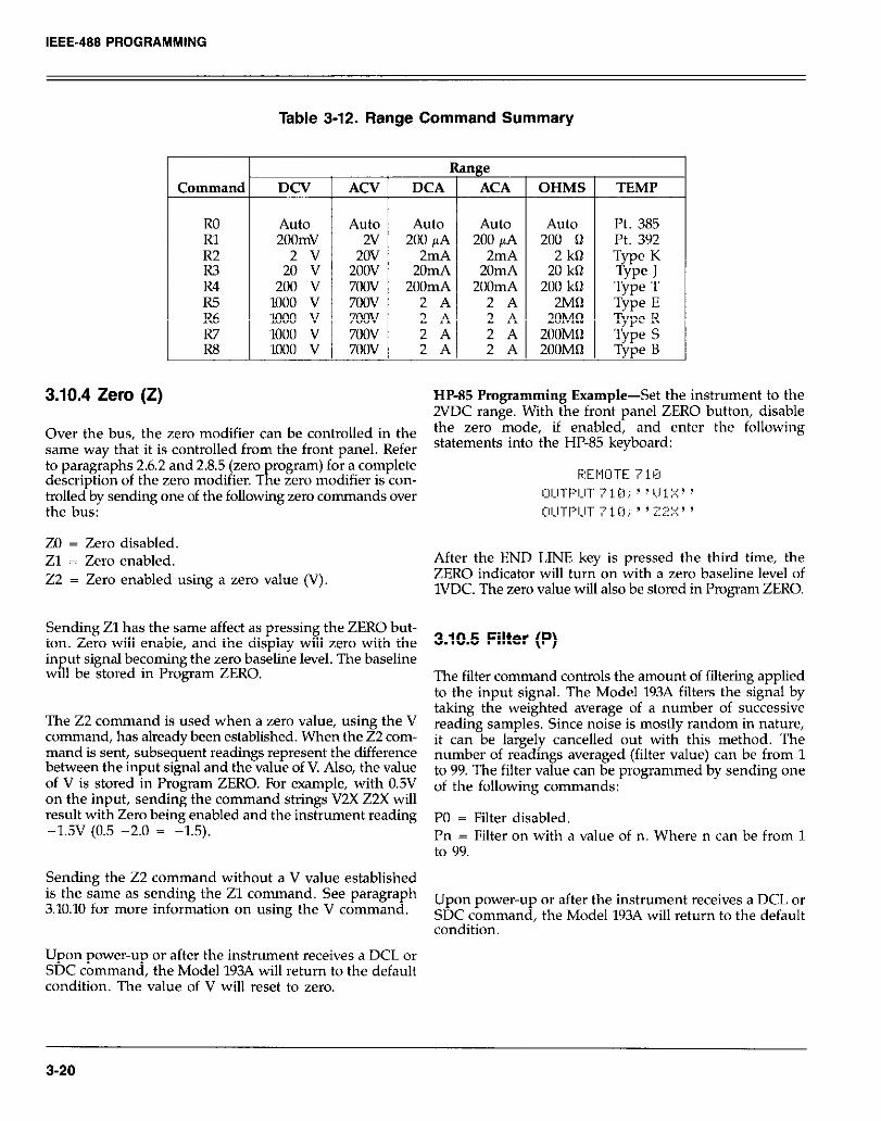
IEEE-488 PROGRAMMING
Table 3-12. Range Command Summary
L
L
COltUlliWl< DCV
RO Rl R2 R3 R4 R5 R6 R7 R8
Auto 2oomv
2; “v 200 v
1000 v 1000 v 1000 v 1000 v
T
3.10.4 Zero (2) HP-85 Programming Example-Set the instrument to the 2VDC range. With the front panel ZERO button, disable
Over the bus, the zero modifier can be controlled in the the zero mode, if enabled, and enter the following
same way that it is controlled from the front panel. Refer statements into the HP-85 keyboard:
to paragraphs 2.6.2 and 2.8.5 (zero description of the zero modifier. R
rogram) for a complete T e zero modifier is con- F:EMOTE 7
trolled by sending one of the following zero commands over UCITF’CIT 71.K *
18
? I,, 1 ‘:.? ? ? II
7 7.:,1..., II II LL,..,
ACV T
Auto 2v
2ov 2oov 7oov 7oov 7oOV 7oov 7oov
2A 2A 2A 2A
OHMS TEMP
Auto Pt. 385 200 0 Pt. 392
2 kfl T pe K 20 k0 J YP~ J
200 kfl Type T 2Mn Type E
20M0 TYPO R 200MQ Type S 200MO TYPO B
1
the bus: -
ZO = Zero disabled. Zl = Zero enabled. 22 = Zero enabled using a zero value (V)
After the ENU LINE key is pressed the third time, the ZERO indicator will turn on with a zero baseline level of 1VDC. The zero value will also be stored in Program ZERO.
Sending Zl has the same affect as pressing the ZERO but- ton. Zero will enable, and the display will zero with the in
7 ut signal becoming the zero baseline level. The baseline
WI 1 be stored in Program ZERO.
The 22 command is used when a zero value, using the V command, has already been established. When the 22 com- mand is sent, subsequent readings represent the difference between the input signal and the value of V. Also, the value of V is stored in Program ZERO. For example, with 0.5V on the input, sending the command strings V2X Z2X will result with Zero being enabled and the instrument reading -1.5v (0.5 -2.0 = -1.5).
Sending the 22 command without a V value established is the same as sending the Zl command. See paragraph 3.10.10 for more information on using the V command.
Upon power-up or after the instrument receives a DCL or SDC command, the Model 193A will return to the default condition. The value of V will reset to zero.
3.10.5 Filter (P)
The filter command controls the amount of filtering applied to the input signal. The Model 193A filters the signal by taking the weighted average of a number of successive reading samples. Since noise is mostly random in nature, it can be largely cancelled out with this method. The number of readings averaged (filter value) can be from 1 to 99. The filter value can be programmed by sending one of the following commands:
PO = Filter disabled. Pn = Filter on with a value of n. Where n can be from 1 to 99.
Upon power-up or after the instrument receives a DCL or SDC command, the Model 193A will return to the default condition.
3-20

IEEE-488 PROGRAMMING
Notes:
1. A filter value sent over the bus is stored in Program FILTER, replacing the previous filter value.
2. Keep in mind that each function can have its own unique filter value.
HP-85 Programming Ewample+‘ith the front panel FILTER indicator off, enter the following statements into the HP-85:
When the END LINE key is pressed the second time, the filter will turn on and have a filter value of 20.
3.10.6 Rate (S)
The rate command controls the integration period and the usable resolution of the Model 193A. The rate commands are as follows:
SO = 3l8rmsec integration at 3%d resolution Sl = 2.59msec integration at 4%d resolution 52 = Line cycle integration* at 51%d resolution 53 = Line cycle integration* at 6%d resolution * 20msec for 50Hz and 16.6msec for 60Hz
Upon power-up or after the instrument receives a DCL or SDC command, the Model 193A will return to the default condition.
HP-85 Programming Exam le-Using RESOLN button, set the disp P
the front panel ay of the Model 193A for 6%d
resolution. Now enter the following statements into the HP-85:
When END LINE is pressed the second time, the Sl rate will be selected.
3.10.7 Trigger Mode (T)
Triggering provides a stimulus to begin a reading conver- sion within the instrument. Triggering may be done in two
basic ways: in a continuous mode, a single trigger com- mand is used to start a continuous series of readings; in a one-shot trigger mode, a separate trigger stimulus is re- quired to start each conversion. The Model 193A has eight trigger commands as follows:
Ttl = Continuous On Talk ll = One-shot On Talk T2 = Continuous On GET 13 = One-shot On GET T4 = Continuous On X T5 = One-shot on X T6 = Continuous On External Trigger T7 = One-shot On External Trigger
The trigger modes are paired according to the type of stimulus that is used to trigger the instrument. In the Tl) and ‘ll modes, triggering is performed by addressing the Model 193A to talk. In the T2 and T3 modes, the IEEE-488 multiline GET command performs the trigger function. The instrument execute (X) character provides the tri er stimulus in the T4 and T5 modes. External trigger pu ses ‘iR provide the trigger stimulus in the Th and T7 modes.
Upon power-up or after the instrument recei\w a DCL or SDC command, the Model 193A will return to the default condition.
HP-85 Programming Example--Place the instrument in the one-shot on talk mode with the following statements:
One reading can now be triggered and the resulting data obtained with the following statements:
In this example, the ENTER statement addresses the Model 193A to talk, at which When the reading has &
oint a single reading is triggered. een processed, it is sent out owr
to the bus to the computer, which then displays the result.
Each time the IBRD function is called, the instrument is addressed to talk, at which time it is triggered. When the conversion is complete, the reading is sent out over the bus to the computer, which then displays the resulting data.
3-21

3.10.9 Reading Mode (B)
The reading mode command parameters allow the selec- tion of the source of data that is transmitted over the IEEE488 bus. Throu h this command, the user has a choice of data from the A /?I converter (normal DMM readings) or the buffer (data store). The reading mode commands are as follows:
80 = A/D Converter readings 81 = Data Store readings
Upon power-up or after the instrument receives a DCL or SDC command, the Model 193A will return to the default condition.
When in BO, normal A/D readings will be sent. In a con- tinuous trigger mode, readings will be updated at the con- version rate. The Bl command is used to access readings from the buffer. When the 81 command is sent, subsequent readings will be taken from consecutive buffer locations beginnin readings 8,
with the first memory location (001). Once all ave been requested, the unit will cycle back and
begin again.
HP-85 Programming Example-From the front panel, store some readings in the data store. Enter the following statements into the computer to read the stored reading in the first memory location of the buffer. The reading will be displayed on the computer CRT.
The second statement above sets the instrument to the buf- fer reading mode. The third and fourth statements acquire the reading and display it on the CRT.
3.10.9 Data Store Interval (Q) and Size (I)
The data store is controlled by the interval command (Q) and the size command (I). The storage process will start when the appropriate trigger is received.
With the Q command, the user can select the interval that the instrument will store readings or select the one-shot mode. In the one-shot mode, one reading will be stored each time the instrument is triggered. The Q command is in the following form:
QO=One-shot into buffer Qn=Set storage interval in millisec (lmsec to 999999msec)
To use the data store in the one-shot mode (QO), the in- strument must be in a one-shot trigger mode (Tl, T3, T5 or T7). In the QCITI mode, one reading will be stored each time the instrument is addressed to talk. In the QlJI3 mode, each GET command will cause one reading to be stored. In the QOT5 mode, each instrument execute character (X) will cause a reading to be stored. Finally, in the QOT7 mode, each external trigger pulse will cause a reading to be stored. If the instrument is in a continuous trigger mode (PZ, T2, T4 or T6), an IDDC error will occur.
To store readings at a selected interval (Qn), the instrument can be in any trigger mode. When the selected trigger oc- curs, the storage process will commence.
The size of the data store can be controlled by one of the following I commands.
IO=Continuous storage mode. In=Set data store size to n (1 to 500).
In the continuous data tom stop after the buffer is fille 2
e mode (IO), storage will not (500 readings), but will pro-
teed back to the first memory location and start overwriting data. With the Innn command, the storage process will stop when the defined number of readings have been stored. In this case the buffer is considered to be full.
Notes:
1. With the instrument in the T6 or T7 external triaer mode, the storage process can be started by pressing the front panel TRIGGER button after the instrument is returned to local operation (LQCAL button).
2. The data store is disable by sending an F command that places the instrument in a different function.
3. The instrument must be in a valid operating state in order to use the high speed data store capabilities. The high speed intervals are lms, 2ms, 3ms and 4ms. Valid com- mands are listed in Table 3-13.
4. With S2 or S3 asserted, the fastest valid storage interval (I) is 40msec. An interval less than 40msec will result in a short period error when the storage process is started. Readings will be stored as fast as the instrument can run.
5. Either during or after the storage process, readings may be recalled by using the Bl command as described in the last paragraph. Also, the highest, lowest and average reading in a full buffer can be recalled by sending the appropriate U commands. See paragraph 3.10.18 for in- formation on using the U commands.
3-22

IEEE-488 PROGRAMMING
Upon power-up or after the instrument receives a DCL or SDC command, the Model 193A will return to the default condition.
HP-85 Pro to enable li
ramming Example-Enter the program below ata store operation and obtain and display 100
readings on the computer CRT:
Display it. y Loop back and get next reading
After entering the program, press the HP-85 RUN key. The program will set the Model 193A to trigger on GET (line 27), set the interval and size (line 30), enable the data store (line 35), wait for memory to fill (lines 40 and 50), turn on the data store output (line 60), and then request and display all 100 readings (lines 70-100).
3.10.10 Value (V) and Calibration (C)
One advanced feature of the Model 193A is its digital calibration capabilities. Instead of the more difficult method of adjusting a number of otentiometers, the user need onl! apply an appropriate call rahon signal and send the calibr+
.g
tion value over the bus.
The V command is also used to program a zero value (see paragraph 3.10.4) and to set the reference junction tenl- perature needed to make thermocouple (TC) measurements (see paragraph 3.10.22).
The value command may take on either of the following forms:
Vllll.lllllllln Vn.nnnnnnE+n
Thus, the following two commands would be equivalent:
v20 V2.OE+l
In this example, note that only as many significant digits as necessary need be sent. In this case, the exact valw iz assumed to be 2O.ooOOU even though only thr first t\\-o digits were actually sent.
Digital Calibration-When performing digital calibration, two points must be calibrated on each range. The first calibration value should be approximately full range and the second calibration values should be approximately zero After the second calibration value is ent over the bus, per- manent storage of the two values will occur.
Table 3-13. High Speed Data Store
Valid Data Data Store Interval Store Size* Valid Functions Valid Ranges
QL Q2 FO, Fl, F3 All, except
Q3, 04 I1 - 1500 M, F7, F8 RO
*Data store size IO (continuous) cannot be used in the high speed data store mode.
Valid Read& Rates
SO
so, 5-3
3-23

In order to send calibration values over the bus, the calibra- tion command (C) must be sent after the value commnd (V) is sent. The calibration command takes on the follow- ing form:
CO = Calibrate first point using value (V) Cl = Calibration second point using value (V)
The following example first sends a calibration value of 2 and then a calibration of 0.
v2xcox VOXClX
If the calibration value is greater than ZZOOOM) counts (at 6%d resolution) an IDDCO error message will be displayed on the Model 193A (see paragraph 3.11.1).
CAUTION Precision calibration signals, must be connected to the instrument before attemotina calibration otherwise, instrument accuracy’will”bs affected. See Section 6 for complete details on calibrating the instrument either from the front panel or over the bus.
NOTE The calibration switch must be in the UNLOCK position before calibration can be accomplished.
When the second statement is executed, calibration of the high end of the 200VDC range is performed, assuming that the correct calibration value is applied to the instrument. When the third statement is executed, calibration of the low end of the ZOOVDC range is performed and permanent storage of the two calibration points take place.
3.10.11 Default Conditions (L)
The LO command allows the user to return the instrument to the factory default conditions. Factory default conditions
are set at the factory and are listed in Table 3-10. The in- strument will then power up to these default conditions. The current IEEE address and line frequency setting of the instrument are not affected by the LO command.
The Ll command is used to save the current instrument conditions. The instrument will then power up to these default conditions.
The L command options are as follows:
L&Restore instrument to factory power-up default conditions.
Ll=Store present machine states as the power-up default conditions.
HP-85 Programming Example-Set the Model 193A to the ohms function, and enable zero and filter. Now, enter the following statements into the computer:
After pressing END LINE the second time, cycle power on the Model 193A and note that the instrument returns to the conditions initially set in this example.
3.10.12 Data Format (G)
The G command controls the format of the data that the instrument sends over the bus. Readings may be sent with or without prefixes. Prefixes are the mnemonics preceding the reading and the buffer memory location. Figure 3-9 fur- ther clarifies the general data format. The G commands are as follows:
GO = Send single reading with prefixes. Examples: NDCV-1.234567E+O (A/D reading) NDCV-1,234567E+O,BOOl (buffer reading)
Gl = Send single reading without prefixes. Examples: -1.234567EcO (A/D reading) -1.234567E+O,OOl (buffer reading)
G2 = Send all buffer readings, separated by commas, with prefixes and buffer memory locations. Examples: NDCV-1.234567E+0,B001,NDCV-1.765432E+0,8002, etc...
G3 = Send all buffer readin s, separated by commas, without prefixes and with % uffer memory locations.
I
-1.234567E+0,001,~1.765432E+0,002, etc
3-24
IEEE-488 PROGRAMMING
G4 = Send all buffer readings, separated by commas, with reading prefixes and without memory buffer locations. Example: NDCV-1,234567E+O,NDCV-1,765432E+O,etc...
G5 = Send all buffer readings, se without reading prefixes and wit .f:
arated by commas, out buffer memory
locations. Example: -1,234567E+O,-1.765432Ec0, etc...
U g B
on power-u or after the instrument receives a DCL or S Ccomman , the Model 193A will return to the default condition.
Notes:
1. The B command affects the source of the data. In the 80 mode, the bus data will come from the A/D converter. In the 81 mode, the data will come from the buffer.
2. The Bl command must be asserted when using the G2 through G5 modes.
3. Programmed terminator and EOI sequences appear at the end of each reading in the GO and Gl modes, but are transmitted only at the end of the buffer in the G2 through G5 modes. No terminator is sent if in G2 through G5 modes while in BO (data from A/D).
HP-85 Programming Example-To place the instrument in the Gl mode and obtain a reading, enter the following statements into the HP-85 keyboard:
When the second statement is executed, the instrument will than data 9
e to the Gl mode. The last two statements acquire rom the instrument and display the reading string
on the CRT. Note that no prefix or suffix appears on the data string.
3.10.13 SRQ Mask(M) and Status Byte Format
The SRQ command controls which of a number of condi- tions within the Model 193A will cause the instrument to request service from the conroller by asserting SRQ. Once an SRQ is generated, that status byte can be checked to determine if the Model 193A was the instrument that asserted SRQ, and if so, what conditions can be checked by using the Ul command, as described in paragraph 3.10.16.
The Model 193A can be programmed to generate an SRQ under one or more of the following conditions:
1. When a reading is completed or an overrange condition
2. If an IDDC, IDDCO, No Remote error occurs, or Scli- Test fails.
3. When the data store is full. 4. When the data store is % full. 5. If a trigger overrun error occurs. 6. When the bus is ready.
Upon power-up or after a DCL or SDC command is re- ceived, SRQ is disabled.
SRQ Mask--The Model 193A usts an internal mask to drter- mine which conditions will cause an SRQ to be generated. Figure 3.10 shows the general format of this mask.
SRQ can be pro rammed by sending the ASCII letter “hl” followed by a 2. earnal number to set the appropriate bit in the SRQ mask. Decimal values for the various hits are summarized in Table 3-14. Note that the instrument may be programmed for more than one set of conditions simultaneously. To do so, simply add up the decimal bit values for the required SRQ conditions. For example, to enable SRQ under reading overflow and buffer full condi- tions, send M5X. To disable SRQ send MOX. This com- mand will clear all bits in the SRQ mask.
3-25

IEEE-488 PROGRAMMING
OEGC = “c- DEGF = “F
1 I
1 /L (B, MODE ONLY)
J-
J
Figure 3-9. General Data Format
Figure 3-10. SRQ Mask and Status Byte Format
3-26

IEEE-488 PROGRAMMING
Table 3-14. SRQ Command Parameters
Command ICondition to Generate SRQ I
MO Disable Ml Reading Overflow
E Data Store Full Data Store ‘/z Full
M8 Reading Done Ml6 Ready M32 Err01
Status Byte Format-The status byte contains information relating to data and error conditions within the inshument. The general format of the status byte (which is obtained by using the serial polling sequence, as described in paragraph 3.98) is shown in Figure 3-10.
The bits in the status (serial poll) byte have the following meanings:
Bit 0 (Reading Overflow)-Set when a” overrange input is applied to the instrument.
Bit 1 (Buffer Full)-!% when the defined buffer size is full.
pftI(lBUffer % Full)-% when half the defined buffer size
Bit 3 (Reading Done)-Set when the instrument has com- pleted the present reading conversion.
Bit 4 (Ready)-Set when the instrument has processed all previously received commands and is ready to accept ad- ditional commands over the bus.
Bit 5 (Error)-Set when one of the following errors have occurred:
1. Trigger Overrun 2. Short Period 3. Uncalibrated 4. Needs Model 1930 5. Needs Model 1931 6. Needs Model 1930 and 1931 7. Cal locked 8. Conflict 9. Translator
10. No Remote 11. IDDC 12. IDDCO 13. String Overflow
The nature of the error can be determined with the Ul com- mand as explained in paragraph 3.10.16. An explanation of each error can also be found in paragraph 3.10.16.
Bit 6 (SRQ)--Provides a means to determine if SRQ was asserted by the Model 193A. If this bit is set, service was requested by the instrument.
Bit 7-Not used and always set to zero
Note that the status byte should be read to clear the SRQ line once the instrument has generated an SRQ. All bits in the status byte will be latched when the SRQ is generated. Bit 6 (RQS) will be cleared when the status byte is read.
HP-85 Programming Example-Enter the following pm gram into the HP-85:
PROGRAM COMMENTS
tion, ‘clear instrum& Program for SRQ o” IDDCO. Attempt to program illegal option. Serial poll the instrument. Wait for SRQ error.
Identify the bits.
Loop eight times. Display each bit position.
Once the program is en&red and checked for errors, press the HP-85 RUN key. The computer first places the instru- ment in remote (line 10) and then programs the SRQ mode of the instrument (line 20). Line 30 then attempts to pro- gram a” illegal command option, at which point the in- strument generates a” SRQ and sets the bus error bit in its status byte. The computer then serial polls the instru- ment (line 4O), and then displays the status byte bits in pro- per order on the CRT. In this example, the SRQ (86) and error (B5) bits are set because of the attempt to program an illegal command option (K5). Other bits may also be set depending on instrument status.
3-27

IEEE-466 PROGRAMMING
3.10.14 EOI and Bus Hold-off Modes (K)
The K command allows control over whether or not the in- strument sends the EOI command at the end of its data
stri?? and whether or not bus activity is held off (through
the RFD lme) until all commands sent to the instrument are internally processed once the instrument receives the X character. K command options include:
KO = Send EOI with last byte; hold off bus until com- mands processed on X.
Kl = Do not send EOI with last byte; hold off bus until commands processed on X.
K2 = Send EOI with last byte; do not hold off bus on X. K3 = Send no EOI with last byte; do not hold off bus on X.
Upon-power up, or after the instrument receives a DCL or SDC command, the instrument will return to the default condition.
The EOI line on the IEEE-488 bus provides a method to positively identify the last byte in a multi-byte transfer se- quence. Keep in mind that some controllers rely on EOI to terminate their input sequences. In this case, suppress- ing EOI with the K command may cause the controller in- put sequence to hang unless other terminator sequences are used.
The bus hold off mode allows the instrument to temporarily hold up bus operation when it receives the X character until it processes all commands sent in the command string. The purpose of the hold off is to ensure that the front end FETs and relays are properly configured before taking a reading. Keep in mind that all bus operation will cease-not just ac- tivity associated with the Model 193A. The advantage of this mode is that no bus commands will be missed while the instrument is processing commands previously received.
The hold off period depends on the commands being pro- cessed. Table 3-15 lists hold off times for a number of dif- ferent commands. Since a NRFD hold off is employed, the handshake sequence for the X character is complete.
NOTE With KO or Kl asserted, hold-off will also occur on an EOI and a terminator. These delays allow for proper operation of the Translator software, since “X” cannot be used in Translator words.
HP-85 Programming Example-To program the instrument for the K2 mode, enter the following statements into the HP-85:
When the second statement is executed, the instrument will be placed in the K2 mode. In this mode, EOI will still be transmitted at the end of the data string, but the bus hold- off mode will be disabled.
Table 3-15. Bus Hold-off Times
Commands
Function (F)
Calibrate (C)
Other
Bus Held Off On X for: I
160mS typical (ACV and ACA functions 660mS typical) Depends on range and function as the calibration is actually per- formed during the hold off time. ex: 1OOOVDC = 9sec. 2OOMO = 19sec 117mS to 200mS typical depen-
I dinz on the command sent,
3.10.15 Terminator (Y)
The terminator sequence that marks the end of the instru- ment’s data string or status word can be programmed by sending the Y command followed by an appropriate ASCII character. The default terminator sequence is the commonly used carriage return, line feed (CR LF) sequence (CR=ASCII 13; LF=ASCII 10). The terminator will assume this default value upon power up, or after the instrument receives a DCL or SDC command.
The terminator sequence may be changed by sending the desired one or two characters after the Y command. Any ASCII character, except one of the following may be used:
I. All capital letters 2. All numbers 3. Blank 4. + - / , and e 5. Semicolon (;)-Used exclusively as a reserved character
for Translator software.
3-26

IEEE-488 PROGRAMMING
Special command sequences will program the instrument as follows:
1. Y?nX = One terminator character. 2. YmnX = Two terminator characters. 3. YX = No terminator.
NOTE Most controllers use the CR or LF character to ter- minate their input sequences. Using a nonstan- dard terminator may cause the controller to hang up unless special programming is used.
HP-85 Programming Example-To reserve the default (CR LF) terminator sequence, type the following lines into the computer:
When the second statement is executed, the normal ter- minator sequence will be reserved; the instrument will ter- minate each data string or status word with a (LF CR) sequence.
3.10.16 Status (U)
The status command allows access to information concer- ning various operating modes and conditions of the Model 193A. Status commands include:
UO = Send machine status word. Ul = Send error conditions. U2 = List Translator words. U3 = Send a value indicating the buffer size. U4 = Send the average reading in the data store. U5 = Send the lowest reading in the data store. U6 = Send the highest reading in the data store. U7 = Send the current value (V).
When the command sequence UOX is transmitted, the in- strument will transmit the status word instead of its nor- mal data string the next time it is addressed to talk. The status word will be transmitted only “nce each time the UO command is given. To make sure that correct status is transmitted, the status word should be requested as soon as possible after the command is transmitted.
The format of UO status is shown in Figure 3-11. Note that the letters correspond to modes programmed by the respective device-dependent commands. The default values in the status word are also shown in Figure 3-11.
Note that all returned values except for those associated with the terminator correspond to the programmed numeric values. For example, if the instrument is present- ly in the R3 range, the second (R) byte in the status Ward will correspond to an ASCII 3. The returned terminator characters are derived by ORing the actual terminator byte values with 530. For example, a CR character has a decimal value of 13, which equals 50D in hexadecimal notation. 0% ing this value with 530 yields $3D or 6~110, which prints out as an ASCII equal sign (=). This terminator conver- sion step is necessary to convert the standard terminators into displayable form, as they will not normally print out on a computer CRT.
The Ul command allows access t” Model 193A errw cw,- ditions in a similar manner. Once the sequence UIX is sent. the instrument will transmit the error conditions with the format shown in Figure 3-12 the next time it is addressed t” talk in the normal manner. The error condition uwrd will be sent only once each time the L’l wmmand is transmitted. Note that the ermr condition M.“rd is xturll- ly a string of ASCII characters representing binary bit posi- tions. An emor condition is also flagged in the status (serial poll) byte, and the instrument can be programmed 1” generate an SRQ when an error condition occurs. See para raph 3.10.15. Note that all bits in the error condition w”r t? and the status byte error bit will be cleared when the word is read. In addition, SRQ operation will be restored after an err”r condition by reading Ul.
The various bits in the error condition \vord ore drs- cribed as follows:
Trigger Overrun-Set when the instrument receives a trig- ger while it is still processing a reading fr”m a prr\,ious trigger.
Short Period-Set when the instrument cannot run as fast as the selected data store interval.
String Overflow-Set if m”re than a 14 character message is sent using the display (D) command.
Uncalibrated-Set when E’I’ROM menwry fails the self test.
Needs Model 1930-Set when the ACV function is selected with the ACV option not installed.
3-29

IEEE-488 PROGRAMMING
Figure 3-11. UO Status Word and Default Values
3-30

IEEE-488 PROGRAMMING
Needs Model 1931-S& when the DCA function is selected with the current option not installed.
Needs Model 1930 and 1931-S& when the ACA function is selected with both the ACV and current options not installed.
Cal Locked-Set when trying to calibrate the instrument with the calibration switch in the locked position.
Conflict-Set when trying to calibrate the instrument while it is in a” improper state.
TRANSERR 09-Translator error. Set when them is no more memory left for Translator words.
No Remote-Set when a progamming command is receiv- ed when REN is false.
IDDC-Set when a” illegal device-dependent command (IDDC), such as EIX is received (“E” is illegal).
IDDCO-Set when a” illegal device-dependent command option (IDDCO) such as l9X is received (“9” is illegal).
NOTE The complete command string will be ignored if an IDDC, IDDCO or no remote error occurs.
TRANSERR 14-Translator error. Set when more than one ALIAS is used in a definition.
‘TRANSERR 15-Translator error. Set when a Translator word exceeds 31 characters.
TRANSERR lh-Translator error. Set when an X is used in a Translator word.
TRANSERR 17-Translator error. Set when trying to define a Translator word that already exists.
TRANSERR 18-Translator error. Set when a $ is used in a Translator word.
TRANSERR 19-Translator error. Set when the ; character is sent while in the NEW mode.
TRANSERR ZO-Translator error. Set when LIST is used in a Translator definition,
TRANSERR Zl-Translator error. Set when FORGET is us- ed in a Translator definition.
TRANSERR 23-Translator error. Set when SAVE is used in a Translator definition.
The U2 command lists the Translator words that have bee11 defined by the operator. The list will be transmitted onl! once each time the command is received.
The U3 command allows the user to find out the current defined size of the buffer. The buffer sire is controlled b\ the I command. When this command is transmitted, th; instrument will transntit the value the next time it is ad- dressed to talk. This information will be transmitted onh once each time the command is received. The U3 value lviil not be cleared when read; thus, the U3 value is alrva~s current.
The U4 command sends the average of all the readings that are in the data store. The U5 conunand sends the lo\vest reading in the data store and the Uh command sends the highest. When any of these commands are transmitted, the instrument will send the appropriate reading the next time the instrument is addressed to talk. A reading will only be sent once each time the appropriate command is received. Transmission of U4, U5 and U6 will not occur until the buf- fer is full.
The U7 command sends the current value. The value ca” be a calibration value, zero value or temperature compcn~ sation value.
HP-85 Programming Example-Enter the following statements into the computer to obtain and display all the status conditions (UO through U7) of the Model 193A.
3-31
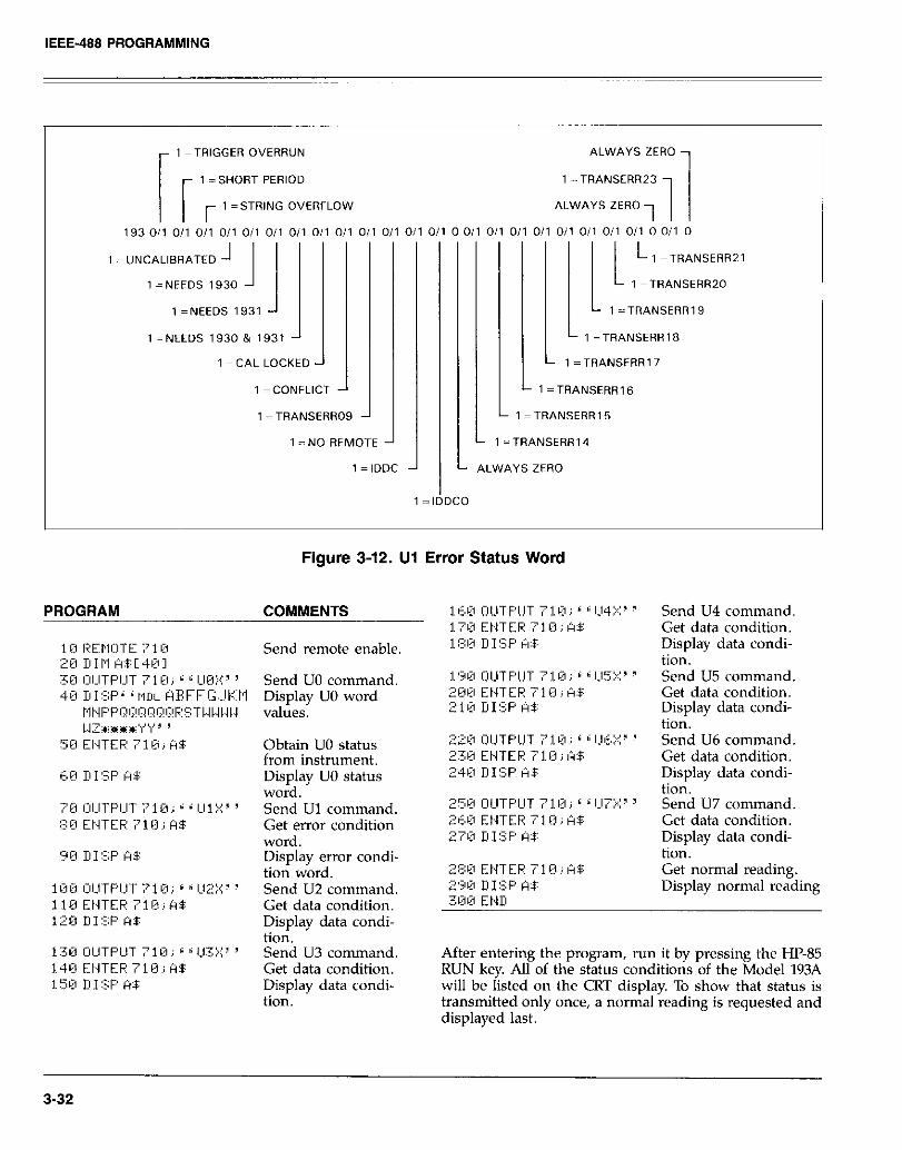
IEEE-488 PROGRAMMING
Figure 3-12. Ul Error Status Word
PROGRAM COMMENTS
Send remote enable.
from instrument. Display UO status word. Send Ul command. Get error condition word. Display error condi- tion word. Send U2 command. Get data condition. Display data condi- tion. Send U3 command. Get data condition. Display data condi- tion.
Send U4 command. Get data condition. Display data condi- tion. Send U5 command. Get data condition. Display data condi- tion. Send U6 command. Get data condition. Display data condi- tion. Send U7 command. Get data condition. Display data condi- tion. Get normal reading. Display normal reading
After entering the program, run it by pressing the HP-85 RUN key. All of the status conditions of the Model 193A will be listed on the CRT display. To show that status is transmitted only once, a normal reading is requested and displayed last.
3-32

IEEE-488 PROGRAMMING
3.10.17 Multiplex (A)
The Model 193A has built-in multiplex routines that automatically calibrate and zero the instrument, so as to maintain its high accuracy. The multiplex routines can be defeated, either through front panel Program 95 (paragraph 2.8.14) or through one of the following commands:
A0 = Disable Multiplex Al = Enable Multiplex
Upon power-up or after a DCL or SDC command, the in- strument will return to the default condition.
HP-85 Programming Example-Disable multiplex by enter- ing the following statements into the HP-85:
When the END LINE key is pressed the second time, the multiplexer routines will disable.
3.10.18 Delay (W)
The delay command controls the time interval that occurs from the point the instrument is triggered until it begins integration of the input signal. This feature is useful in situations where a specific time period must transpire to allow an input signal to settle before measurement. Dur- ing the delay period, the input multiplexing FETs are switched on so the instrument is set to begin integration upon conclusion of the programmed delay period. A delay period can be programmed using the following command:
Wn
Here, n represents the delay value in milliseconds. The range of programmable delay values is from Omsec to 60000msec.
Example: For a delay of 0.002sec send WZX. For a delay of 30.05sec send X30050X. For a delay of 60%~~ send W6OOOOX.
Upon power-up or after receiving a DCL or SDC com- mand, the instrument will return to the default condition.
HP-85 Programming Example--To program a 250msec delay period into the instrument, enter the following statements into the computer:
REMOTE 710 OUTPUT 71O;“W25OX”
After the END LINE key is pressed the second time, the instrument will wait for 250msec after each triggered cow version before executing the next coversion period.
3.10.19 Self-Test (J)
The J command causes the instrument to perform tests it automatically performs upon power-up. When the self-test command is given, the Model 193A performs the follow ing tests:
1. ROM Test 2. RAM Test 3. E’PROM Test
J command parameters include:
JO = Perform self-test.
If the self-test is successful, the J by& in the UO status word will be set to 1. If E’I’ROM fails, the message “UK CALIBRATED” will be displayed and the J byte in the U1 status word will be set to 2. An E’PROM failure is also flag- ed in the Ul status word. If ROM and RAM fails, the in- strument wilt lock up.
See paragraph 6.9.2 for more information on these tests and recommendations to resolve a failure.
HP-85 Programming Example-Enter the following statements into the computer to perform the h4odet lY3A self-test:
When the END LINE key is pressed the second time, the instrument performs the self-test. If successful, the self-test byte (J) in the UO status word will be set to 1. This byte may be cleared by reading the UO status word (see paragraph 3.10.16).
3-33
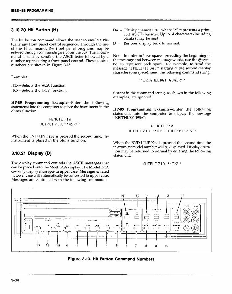
3.10.20 Hit Button (H) Da = Display character “a”, where “a” represents a print- able ASCII character. Up to 14 characters (including
The hit button command allows the user to emulate vir- blanks) may be sent.
tually any front panel control sequence. Through the use D = Restores display back to normal. of the H command, the front aanel rxoeranw tnav be entered through co&ands given’over t&z b&. The H corn- mand is sent by sending the ASCII letter followed by a Note: In order to have spaces preceding the beginning of number representing a front panel control. These control the message and between message words, use the @ sym- numbers are shown in Figure 3-13. bol to represent each space. For example, to send the
messaee “I NEED IT BAD” starting at the second disolav characyer (one space), send the foll&ing command s&in&
Examples:
H3X-Selects the ACA function HOX-Selects the DCV function.
Spaces in the command string, as shown in the following examples, are ignored.
HP-65 Programming Example-Enter the following statements into the computer to place the instrument in the ohms function: HP-85 Programming Example-Enter the following
statements into the computer to display the message
F’E,,i,TE ;:‘I.# “KEITHLEY 193A”:
OlJTF’I.JT 7 1$3 i ‘i 6 II b::E I TtiLE:‘.If? I. ‘3:s ::.:: 1 i
When the END LINE key is pressed the second time, the instrument is placed in the ohms function.
When the END LINE Key is pressed the second time the inshument model number will be displayed. Display opera-
3.10.21 Display (D) tion may be returned to normal by entering the following statement:
The display command controls the ASCII messages that can be placed onto the Moe1 193A display. The Model 193A can only display messages in upper case. Messages entered in lower case will automatically be converted to upper case. Messages are controlled with the following commands:
Figure 3-13. Hit Button Command Numbers
3-34

IEEE-488 PROGRAMMING
3.10.22 Reference Junction (0)
The Model 193A can make temperature measurements us- ing Type K, J, T, E, R, S and B thermocouples (TC’s). In order to make TC temperature measurements the Model 193A must know the temperature of the reference junction. When using the Keithley Model 705 or 706 Scanner with the Model 7057A TC Scanner Card installed, the Model 193A can measure the reference junction. However, if other TC setups are used, the Model 193A must be told the temperature of the reference junction. The following two commands are used to acquire the reference junction temperature:
00 = Measure the reference junction. 01 = Here is the reference junction temperature using
Value (V).
The 00 command measures the reference junction temperature and automatically makes the calculation for the selected TC t
B e. The 00 command can only be used
with the Model 0 or 706 with the Model 7057A installed.
NOTE When the 00 command is sent, an erroneous tem- perature reading of the reference junction will be displayed. This error occurs because the instrument displays a thermocouple measurement of the reference junction. However, this erroneous tem- perature reading does not affect the integrity of the thermocouple linearization process. Thus, when 00 is sent over the bus, i nore the invalid temperature reading that will e dlsplayed. %
The 01 command is used for all other TC setups and is used in conjunction with the V command. The V command in Mp
uts the unknown reference junction temperature to the ode1 193A, and the 01 command enters the value and
makes the required calculation for the selected TC type.
NOTE Reference junction measurements should be made at < 30sec intervals due to possible reference junc- tion temperature drift caused by ambient tempera- ture variations.
Perform the following 1
rocedure to make thermocouple measurements using t e Model 705 Scanner with the Model 7057A. Thermocouple Scanner Card installed:
1. Select the temperature measurement mode by sending F5X (for “F) or F6X (for “C) over the IEEE-488 bus.
2. Send one of the following commands over the bus to select the desired thermocouple type: R2X = Type K R3X = Type J R4X = Type T R5X = Type E R6X = Type R R7X = Type S R8X = Type B
3. Connect the OUTPUT of the thermocouple scanner card to the VOLTS HI and LO input terminals of the Model 193A using copper test leads.
4. Connect a thermocouple to the desired channel (2 through 10) of the thermocouple card.
5. Close channel 1 of the scanner, which is connected to the thermister bridge of the scanner card.
6. Send the following command over the IEEE-488 bus to measure the reference junction temperature on the scam ner card: 00X.
7. Set the Model 705 to the channel that has the thermo- cuple connected to it and close that channel.
8. Thermocouple temperature measurements can no\v be taken directly from the display of the Model 193A.
HP-85 Programming Example-With the Models 705 and 7057A connected to the instrument, connect a Type K ther- mocouple to channel 2 of the scanner card. make sure the IEEE address of the Model 705 is at 17. Enter the following program into the computer to make Type K thermocouple temperature measurements.
COMMENTS Send remote enable. Clear all devices.
junction. 50 OCITPCIT ;I;. . , E:2(:~1'::.:: 7 1 Close channel 2 of
scanner. 70 EHD
Run the program by pressing the RUN key. The Model 193A will be configured for Type K thermocouples, read the reference junction temperature and then take one tempera- ture measurement.
3-35

IEEE-488 PROGRAMMING
Use the following basic procedure to make TC temperature measurements using the 01 command:
Measure and note the temperature of the referrnce junc- tion of the TC setup to be used. Send the appropriate F and R commands over the bus to select the desired scale nad TC type.
Connect thr TC setup to the input of the Model 193A. Using the V command, send the noted referenced junc- tion temperature over the bus to the Model lY3A. Send the value in “C if F6 was asserted and send the value if “F if F5 was asserted. For example, if the instrument is in the “C &mperature mode (F6) and the reference temperature is 25.3”C, then send the following command over the bus: V25.3X. Now send the following command to enter the temperature value and make the required calculation for the selected TC type: 03~X.
6. TC temperature can now be taken directly from the display of the Model 193A.
3.10.23 Exponential Filter (N)
In addition to the digital filter (P), an exponential filter is used to provide additional filtering when making high resolution and high sensitivity measurements. The inter- nal exponential filter is controlled by the following commands:
NO = Internal exponential filter off Nl = Internal exponential filter on
HP-85 Programming Example--Enter the following statements into the computer to turn the exponential filter off:
When the END LINE key is pressed the second time, the exponential filter will disabled.
3.11 FRONT PANEL MESSAGES
The Model 193A has a number of front panel messages associated with IEEE-488 programming. These messages are intended to inform you of certain conditions that oc- cur when sending device-dependent commands to the instrument.
The following paragraphs describe the front panel error messages associated with IEEE-488 programming.
3.11.1 Bus Error
A bus error will occur if the instrument receives a device- dependent command when it is not in remote, or if an il- legal device-dependent command (IDDC) or illegal device- dependent command option (IDDCO) is sent to the instru- ment. Under these conditions, the complete command strin will be rejected and one of the following messages will fe displayed:
NO REMOTE IDDC
IDDCO
NOTE Selecting the ACV, ACA or DCA function over he bus with the appropriate options not installed, will result in an IDDCO message.
In addition, the error bit and pertinent bits in the U1 word will be set (paragraph 3.10.16) and the instrument can be programmed to generate an SRQ under these conditions (paragraph 3.10.13).
A no remote error can occur when a command is sent to the instrument when the REN line is false. Note that the state of REN is only tested when the X character is re- ceived. An IDDC error can occur when an invalid com- mand such as ElX is transmitted (this command is invalid because the instrument has no command associated with that letter). Similarly, an IDDCO error occurs when an in- valid option is sent with a valid command. For example, the command T9X has an invalid option because the instru- ment has no such trigger mode.
HP-85 Programming Example-To demonstrate a bus error, send an IDDC with the following statements:
When the second statement is executed, the bus error message appears on the display for about one second.
3-36

IEEE-488 PROGRAMMING
3.11.2 Trigger Overrun Error
A trigger overrun error occurs when the instrument receives a trigger while still processing a reading from a previous trigger. Note that only the overrun triggers are ignored. These overrun triggers will not effect the instrument except to generate the message below. When a trigger overrun oc- curs, the following front panel message will be displayed for approximately one second:
TRIG-OVERRUN
HP-85 Programming Example-To demonstrate a trigger overrun error, enter the following statements into the HP-85 keyboard:
Note that the trigger overrun message is displayed after the END LINE key is presed a third time.
3.12 BUS DATA TRANSMISSION TIMES
A primary consideration is the length of time it takes to obtain a reading once the instrument is triggered to make a conversion. The len
B th of time will vary somewhat depen-
ding on the selected unchon and trigger mode. Table 3-16 gives typical times.
Table 3-16. Trigger To Reading-Ready Times (DCV Function)
Configuration’ Mode Time (typical)
SOAOGlNmTX Maximum reading hmsec
rate (3Yzd) SMU 3%d mode l2msec s1nx 4%d mode) lhsec SZllX 5%d mode 30msec
s3rlx 6’/zd mode l.lsec
*Commands not listed are at factory default.
3.13 TRANSLATOR SOFTWARE
The built in Translator software allows the user to define his own words in place of Keithley’s defined device- dependent commands. One word can replace a single com- mand or a string of commands. Fur example, the word ACV can be sent in place of Fl, and the word SETUP1 can be sent in place of F3RlT2SOZlUOMZPl5. Also, Keithley com- mands can be translated to emulate functions of other units. For example, the word RA, which is used by H-P to select autorange, can be sent in place of RO. There are certain words and characters that cannot be used as defined Translator words. These reserved words and characters make up the Translator software syntax and are listed in Table 3.17.
3.13.1 Translator Format
The basic format for defining a Translator word is shown in the following example command string, which defines the word SETUP1 as a substitute for FlROX.
“ALIAS SETUP1 FLROX :”
Where:
ALIAS is a reserved word that precedes the Tr.mslator word. SETUP1 is the desired Translator word. FlROX is the Keithley command string. ; is a reserved character necessary to terminate the Translator string. At least one space must be used to separate words and the “:” character.
When SETUP1 is sent over the IEEE-488 bus, the instru- ment will go to the ACV function (Fl) and enable autorange OW.
Translator words that contain conflicting device-dependent commands, such as Fl and F2, can be defined. When send- ing the command word over the bus, the device-dependent command that was last entered will prevail. For example. sending a Translator word in place of FOFlX will place the instrument in the Fl function.
3-37

IEEE-488 PROGRAMMING
Table 3-17. Translator Reserved Words and Character
NEW OLD
SAVE LIST FORGET
Description
Used at the beginning of a command string to define Translator words. Used to terminate the Translator string (one space must precede it). Used to define wild card Translator words. Values sent with a wild card Translator word select options of the equivalent DDC. Tells the Model 193A to recognize Translator words. Tells the Model 193A to only recognize the Keithley device-dependent commands. Saves Translator words as power-up default. Used to list the Translator words. Used to purge Translator words from memory.
Table 3-18. Translator Error Messages
Display Message Explanation
TRANSERR 9 No more memory left for Translator words. TRANSERR14 Use of more than one ALIAS in a definition. TRANSERRW Translator word exceeds 31 characters.
TRANSERR16 Use of an X in a Translator word. TRANSERR17 Trying to define a Translator word that alread)
exists. The second strine in the examule is the
TRANSERR18 TRANSERR19 Sending the : character. TRANSERRZO Use of XIST in a Translator definition. TRANSERRZl I Use of FORGET in a Translator definition TRANSERR23 Use of SAVE in a Translator definition.
Example Error String
“ALIAS TESTl FlX ALIAS TEST2 RlX (” ‘ALIAS ITHINKTHISlSTHlRTYTWOC~ARACT ERS! FlX ;” “ALIAS XRAY FlX ;” “ALIAS SETUP FlX ;” “ALIAS SETUP RlX ;”
“ALIAS 5200 FlX ;” 41.1,
-iLlAS DOG FIX LIST ;” “ALIAS DOG FlX FORGET ;” “ALIAS DOG FIX SAVE ;”
Notes:
1. Trying to define a Translator word that already exists will cause an error messaee to be disolaved brieflv. That Translator word will r&in its wig&i definitiok
2. A Translator word cannot exceed 31 characters. 3. The Translator buffer can hold approximately 100 IB-
character Translator words. 4. The character X and 5 cannot be used in Translator
words. 5. The Model 193A will not recognize an undefined Trans-
lator word sent over the bus. 6. A valid Translator word sent over the bus while the in-
strument is in the OLD mode will not be recognized. However, the instrument will tr X) the letters and numbers of t i
to execute (on the next e word as if they were
device-dependent commands. To avoid this problem, it is recommended that NEW be sent before trying to ex- ecute Translator words. See paragraph 3.23.3 for an ex- planation of NEW and OLD,
3-38
7. Translator error messages are listed and described in Table 3-B.
HP-85 Programming Example-Enter the following pro-
? ram into the computer to define a Translator word SETUPl) to emulate the command string FlROX:
When END LINE is pressed the second time, the Translator word will be defined to emulate the Keithley command string. When END LINE is ressed the third time, the in- strument will go to the AC VP functmn (Fl) and enable auto- range (RO)

IEEE-488 PROGRAMMING
3.13.2 Wild Card ($)
An advanced feature of Translator software is its wild card capabilities. By using the reserved character ‘?$“, the same basic Translator word can be used to select all options of a command. With this feature, a DDC option number is sent with the wild card Translator word. The format for using the wild card is shown in the following example, which defines the word FUNCTION as a substitute for the F command:
‘ALIAS FUNCTION F$X ;” “FUNCTION 1’ “FUNCTION 2”
The first statement defines FUNCTION as the wild card Translator word for the F command. The wild card ($) will allow any valid option number of the F command (0 through 13) to be sent with the word. The second state- ment which is the substitute for the Fl command, will place the instrument in the ACV function. The third statement is a substitute for the F2 command, and will place the in- strument in the ohms function.
Notes:
1. When sending a wild card Translator word over the bus, there must be a space between the Translator word and the option number.
2. If a wild card Translator word is sent without an option number, the instrument will default to option 0.
HP-85 Programming Example-Enter the following pro- gram to define a wild card Translator word to emulate the I’ (filter) command.
The second statement defines FILTER as the wild card Translator word for the P command. The third statement enables the filter with a filter value of 20.
3.13.3 NEW and OLD
NEW is a reserved word that tells the instrument that the ensuing commands may be defined Translator words. The instrument will then respond to the Translator words as well as Keithley device-dependent commands. The re- served word ALIAS automatically places the instrument in the NEW mode. NEW is also used to combine Translator words and is explained in paragraph 3.‘l3.4.
OLD is a reserved word that prevents the instrument from responding to the defined Translator words. In this mode, only the Keithley device-dependent commands will be recognized over the bus.
HP-85 Programming Example-Enter the follo\ving state- ments into the computer to place the instrument in the NEW mode:
When END LINE is pressed the second time, the instrw ment will go into the NEW mode.
3.13.4 Combining Translator Words
Existing Translator words can be combined resulting in a Translator word that contains the commands of the two (or more) combined words. For example, existing Translator words SETUP1 and SETUP2 can be combined and named SETUP3. When SETUP3 is sent over the bus, the commands of both SETUP1 and SHtJI’2 \vill be executed. The format for combining Translator words is shown in the following example:
“ALIAS SETUP3 NEW SETUI’I NEW SETUP2 ;”
Where:
SETUP3 is the new Translator word. SETUP1 and SETUP2 are words to be combined. NEW is a reserved word that tells the instrument that SETUPl and SETUP2 are Translator words and not Kcithle) device-dependent commands.
Even though the two words were combined to form SETUP3, SETUP1 and SETUP2 still exist as valid Translator words.
Wild card Translator words can also be combined with other Translator words. The option number used with the neu word will apply only to the first wild card word in the string. For example, assume that FILTER (emulating the I’ command) and FUNCTION (emulating the F command) are wild card Translator words that are to be combined with the normal Translator word SETUPI. The format might look like this:
“ALIAS TEST NEW SETUP1 NEW FLJNCTIOS NEW FII.TER ;”
3-39

IEEE-488 PROGRAMMING
The new Translator word is TEST. Whenever TEST is sent, the option value sent with that word will only affect func- tion since FUNCTION is the first wild card command in the string. For example, TEST might be sent over the bus in the following format:
“TEST 3”
The “3” in the command string will any affect the FUNC- TION command. In this example the instrument will be placed in the DCA function (F3). Since the FILTER com- mand does not have an assigned option value (due to its position in the string), it will default to 0 (disable).
HP-85 Programming Example-The following program will create two Translator words and then combine them to form a third Translator word:
The second and third program statements define the two Translator words. When END LINE is pressed a fourth time, the two words combine to form the new word (SETUP3).
3.13.5 Combining Translator Words With Keithley IEEE-488 Commands
One or more existing Translator words (including wild card words) can be combined with Keithley IEEE commands resulting in a Translator word that contains the commands of the Translator words and the Keithley IEEE commands. The format for combining Translator words with Keithley IEEE commands is shown in the following example:
“ALIAS SETUP3 NEW SETUP1 NEW SETUP2 PlZlX ;”
Where:
SETUP3 is the new Translator word. SETUP1 and SETUP2 are the existing words. PlZlX is the Keithley IEEE command string. NEW tells the instrument that SETUP1 and SETUP2 are Translator words.
When the Translator word SETUP3 is asserted over the bus, the commands of the two Translator words and the Keithley IEEE command string will be executed.
HP-85 Programming Exam create two Translator war 8
k-The following program will s and then combme them with
a Keithley IEEE command string to form a new Translator word:
The second and third statements create two Translator words. When END LINE is pressed the fourth time, the two Translator words are combined to form the word SETUP3.
3.13.8 Executing Translator Words and Keithley IEEE Commands
Translator words (including wild card words) and Keithley IEEE commands can be executed in the same command string. The format for doing this is demonstrated in the following examples:
“SETUP1 PlZlX” “FUNCTION 2 PlZlX”
When the first command string is sent over the bus, the commands in SETUP1 and the Keithley IEEE commands will be executed. When the second string is sent, the se- cond option of the wild card FUNCTION command and the Keithley IEEE commands will be executed.
HP-85 Programming Example-The following program will assert the commands of an existing Translator word and the standard Keithley IEEE commands over the bus:
When END LINE is pressed the second time, the com- mands of SETUP1 and the Keithley IEEE commands (PlZlX) will be sent over the bus.
3-40

IEEE-488 PROGRAMMING
3.13.7 SAVE
Translator words can be remembered by the instrument as power up default words by sending the reserved word SAVE. If SAVE is not sent, Translator words will be lost when the instrument is turned off.
When SAVE is sent, the instrument also remembers if it was in NEW or OLD. If the instrument is in NEW when SAVE is sent, it will ower up in NEW. If the instrument is in OLD when SA E IS sent, it will power up in OLD. s,
HP-85 Programming Example-With one or moth Translator words already defined, enter the following statements in- to the computer to retain them as power up default words:
F:EIIOTE 7113
OI_ITPI_IT 71d.i 6 c :I;AI.jE” !
When END LINE is pressed the second time, current Translator words will become power up default words.
3.13.8 LIST
LIST is a reserved word that can be used to list the existing Translator words stored in temporary memory. The most recent defined word will be listed first.
Notes:
1. The U2 command can also be used to list the Translator words (see paragraph 3.10.16).
2. If there are no Translator words in memory, nothing will be displayed when the list is requested.
HP-85 Programming Example--With Translator words already defined, enter he following program statements to list them:
The second and third statements will send the word list to the computer. When END LINE is pressed a fourth time, the Translator words will be displayed.
3.13.9 FORGET
FORGET is a reserved word that is used to purge all Translator words from temporary memory However, Translator words that were saved in E’PROM by the SAVE command will again be available after power to the instru- ment is cycled.
To purge Translator words from E’PKOM, first send the FORGET command and then send the SAVE command.
HP-85 Programming Example-Enter the following statements into the computer to purge all Translator words from temporary memory:
When END LINE is pressed the second time, the Translator words are purged from temporary memory.
3-41

IEEE-488 PROGRAMMING
3.3.10 Program Modifications
In order for the Translator to function properly, a <CR> <LF> terminator sequence must be appended to the end of any Translator execution sting sent to the instrument. With normal device-dependent commands, the instru- ment holds off the bus upon receipt of the “X” character until it completes command execution. With Translator words, however, “X” cannot be included in the command string, so no bus hold off occurs, and the commands can- not execute properly. Adding the <CR> <LF> sequence to the end of the Translator execution string ensures that the bus is held off until the command is executed.
Model 8573A and National Instruments GPIB-PC Cards
From BASIC, the <CR> <LF> sequence can be added to the Translator execution string as in the example below.
100 CMD$=“ALIAS RANGE ROX;”
110 CALL IBWRT (M193A%,CMD$)
Define Translator word.
Send word to unit.
120 CMD$=“RANGE” Define Translator com- mand.
130 CMD$=CMD$+ Append <CR> <LF> to CHR5(13)+CHR5(10) string.
140 CALL IBWRT Send appended string. (M193A%,CMD$)
CEC PC-488 Cards
The necessary <CR> <LF> terminator sequence can be added from BASIC as in the example shown below.
100 CMD$=“ALIAS Define Translator word. RANGE ROX;”
110 CALL SEND Send word to unit. (ADDR%. CMD$. STATUS%)MIP~A%, CMD$)
120 CMD$=“RANGFY’ Define Translator com- mand.
130 CMD$=CMD$+ Append <CR> <LF> to CHR$(13)+CHR$(lO) string.
140 CALL SEND Send appended string. (ADDR%,CMD$, STATUS%)
3-42

SECTION 4 PERFORMANCE kERlFlcATl0~
4.1 INTRODUCTION 4.4 RECOMMENDED TEST EQUIPMENT
The procedures outlined in this section may be used to Table 4-l lists all test equipment required for verification. verify that the instrument is operating within the limits Alternate equipment may be used as long as the substitute stated in the s ecifications at the front of this manual. Per- formance ver
&? lcatlon may be performed when the ins&u-
equipment has specifications at least as good as those listed in the table.
ment is first received to ensure that no damage or misad- justment has occurred during shipment. Verification may also be performed whenever there is a question of instru- ment accuracy, or following calibration, if desired.
NOTE The verification limits in this section do not include test equipment tolerance.
NOTE If the instrument is still under warranty (less than 1 year from the date of shipment), and its perfor- mance falls outside the specified range, contact your Keithley representative or the factory to determine the correct course of action.
4.2 ENVIRONMENTAL CONDITIONS
All measurements should be made at 18 28°C (65 82’F) and at less than 80% relative humidity.
4.5 VERIFICATION PROCEDURES
The following paragraphs contain procedures for verifying the 1 year accuracy specifications of the instrument, at 5’,,2 di D P
it resolution, for each of the six measuring functions: volts, TRMS AC volts, ohms, TRMS AC amps. DC amps
and RTD temperature. These procedures are intended for use only by qualified personnel using accurate and reliable test equipment. If the instrument is out of specifications and not under warranty, refer to Section 6 for calibration procedures.
4.3 INITIAL CONDITIONS
The Model 193A must be turned on and allowed to warm up for at least one hour before beginning the verfication procedures. If the instrument has been subject to extremes of temperature (outside the range specified in paragraph 4.2), additional time should be allowed for internal temper- atures to reach normal operating temperature. Typically, it takes one additional hour to stabilize a unit that is 10°C (18°F) outside the specified temperature range.
WARNING The maximum common-mode voltage (voltage between input low and chassis ground) Is 500V. Exceeding thls value may cause a breakdown in insulation, creating a shock hazard. Some of the procedures In this section may expose the user to dangerous voltages. Use standard safety precautions when such dangerous voltages en? encountered.
4-1

PERFORMANCE VERIFICATION
Table 4-1. Recommended Test Equipment
Fluke Fluke
Mfo 1 Model 1 neamintinn Snerifiratinns
Fluke
Fluke
5215A AC Power Amplifier
5450A Resistance Calibrator
Fluke 5700A Calibrator 200~~2A ranges f.03% dc, +O.l% ac to 5kHz Gen. Rad. 143X Decade Resistance *O.Ol%
2oomv, zv, 2ov, 2oov, 1ooov ranges * 15 ppm. ZV, 2OV, 200V ranges; 20M +O.l%; 50Hz-20kHz 0.02%; 100kHz +0.33%. 7OW range: 20Hz +0.12%; 50Hz-20kHz *0.04%; 1OOkHz +O.l% ZOO!L2MQ +15 ppm; 20Mdl *32 ppm; 200Mfl U-5 ppm
4.51 DC Volts Verification 5. Disable zero and leave it disabled for the remainder of the DCV verification procedure.
With the Model 193A set to 5’/2 digit resolution, verify the 6. Check the ZV, 2OV, 200V and 1OOOV ranges by applying DC volts function as follows: the respective DC voltage levels listed in Table 4-2. Verify
to see that the reading for each range is within the limits listed in the table
CAUTION Do not exceed 1OOOV between the inout HI and LO terminals or damage to the instriment may
” ”
occur.
7, Repeat the procedure for each of the ranges with neeative voltaees.
Table 4-2. Limits for DC Volts Verification
1. Select the DCV function and autorange. 2. Connect the DC voltage calibrator to the Model 193A as
shown in Figure 4-l. 3. Set the calibrator to OV and enable zero on the Model
193A. Verify that the display is reading OOO.OOOmV +2 counts.
NOTE Low measurement techniques should be used when checking the 200mVDC range. Refer to para- graph 2.6.5 for low level measurement considera-
4. Set the calibrator to output +ZOOmV and verify that the reading is within the limits listed in Table 4-2.
Applied K DC Volta e Allowable Readings
(W to ZWC)
2oomv 2 v
20 v 200 v
innn v
2OO.OOOmV 2.00000 v 1 20.0000 v 200.000 v 1000.00 v
199.982 to 2oo.ol8 1.99991 to 2.00009 19.9981 to 20.0019 199.981 to 200.019 999.86 to 1000.14
I-- ---- ---- -- - CALIBRATOR --. l
MODEL 193A MODEL 5440A
Figure 4-1. Connections for DC Volts Verification
4-2

4.5.2 TRMS AC Volts Verification 2. Connect the AC calibrator to the Model 193A as shown in Figure 4-2.
With the Model 1930 installed and the instrument set to 3. Set the calibrator to output 2V at n frequency of 20Hz 5% digit resolution, perform the following procedure to and verify that the reading is within the limits listed in verify the AC volts function: Table 4-3.
4. Repeat the 2VAC measurement at the other frequencies specified in Table 4-3.
CAUTION Do not exceed 700V RMS 1OOOV peak 2 x 10⁷V* Hz between the input HI and LO terminals or instru-
5. Repeat the procedure for the 2OV, 200V and 7OOV ranges by applying the respective AC voltages listed in .Tahlr -1.3. Check to see that the readine for each ranze is within
ment damage may occur. the limits listed in the table.”
1. Select the ACV function and autorange. Do not use zero to cancel the offset in this procedure. Turn zero off, if it is enabled.
Figure 4-2. Connections for TRMS AC Volts Verification
Table 4-3. Limits for TRMS AC Volts Verification
193A ACV Range
2v
2ov
2oov
7oOV
Applied AC Voltage
2.ooooov
2.620100 2o.oooov
to 20.2100
2oo.ooov
I-
’ to 202.100
650.00 V
65:50
2Goo~ 2o~P,oo ’ 2o::oo 642.50 646.72 646.72
to to to 653.28 653.28 656.25
DC to 26
20kHz
1.99000 to
2.025.00 19.9000
to 20.2500 199.000
2O:;OO 643.75
) ;
1OOkHz ~
1.97500 i
I 19.7500 /
197500 ;
*
4-3

PERFORMANCE VERIFICATION
Figure 4-3. Maximum input TRMS AC Voltage
4.5.3 Ohms Verification
With the Model 193A set to 5% digit resolution, verify the ohms function as follows:
CAUTION Do not exceed 350V peak or 250V RMS be- tween the input HI and LO terminals or damage to the instrument may occur.
1. Select the ohms function and autorange.
2. Using Kelvin test leads (such as the Keithley Model 1641) connect the resistance calibrator to the Model 193A as shown in Figure 4-4.
3. Set the calibrator to the SHORT position and enable zero on the Model 193A. Verify that the display reads 000.000.
4. Set the calibrator to output 190n and verify that the reading is within the limits listed in Table 4-4.
5. Disable zero and leave it disabled for the remainder of the ohms verification procedure.
6. Utilizing Figures 4-4 and 4-5, check the 2kQ through 200MQ ranges by applying the respective resistance levels listed in Table 4-4. Verify that the readings are within the limits listed in the table.
Figure 4-4. Connections for Ohms Verification (200%20kQ Range)
4-4

PERFORMANCE VERIFICATION
Table 4-4. Limits for Ohms Verification
Applied Allowable Readings 193A Range set-up Resistance WC to 28T)
I /
200 0 Figure 4-4 190.000 R 189.979 to 190.021 2 kR Figure 4-4 1.9C000 kn 1.89979 to 18.9979
20 kfl Figure 4-4 19.0000 k0 1.90021 to 19.0021 200 kQ Figure 4-5 190.000 kO 189.979 to 190.021
2MQ Figure 4-5 1.90000MQ 1.89979 to 1.90021 20Mn Figure 4-5 19.0000MR 18.9865 to 19.Ol35 ~
200MQ Figure 4-5 lOO.OOOMfl 96.798 to 103.202 /
Figure 4-5. Connections for Ohms Verification (200kR-200MQ Ranges)
4.5.4 DC Current Verification 1. Select the DCA function and autorange. 2. Connect the DC current calibration source to the Model
With the Model 1931 installed and the instrument set to 193A as shown in Figure 4-6. 5% digit resolution, verify the DC current function as 3. Set the calibration source to output +2OO,u\ .md verii\ follows: that the reading is within the limits listed in ‘lhble 4-j.
4. Repeat the procedure for the 2mA, 2OmA, 200mA and
CAUTION Do not exceed 2A (or 2.2A for more that 1 1 minute) to the AMPS and LO input terminals or the front panel currant fuse will b low.
2A’ranges 6y applying the respective UC current levels listed in Table 4-5. Check to see that the reading for each range is within the limits listed in the table.
5. Repeat the procedure for each of the ranges with “a”q+:.,., ,-..“..“.., In./elr “L~auYF CUllClll ICYCIJ
Table 4-5. Limits for DC Current Verification
c 193A Range Applied
DC Current
200 PA 200.000 PA 2mA 2.00000mA
20mA 20.0000mA 200mA 200.000mA
2 A 2.00000 A
Allowable Readings (18OC to 2PC)
199.810 to 200.190 1.99810 to 2.00190 19.9810 to 20.0190 199.810 to 200.190 1.99810 to 2.00190
i
4-5
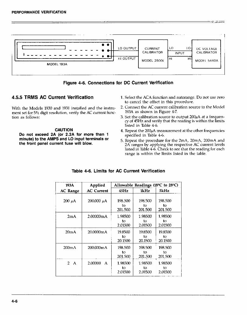
PERFORMANCE VERIFICATION
Figure 4-6. Connections for DC Current Verification
4.5.5 TRMS AC Current Verification
With the Models 1930 and 1931 installed and the instru- ment set for 5% digit resolution, verify the AC current func- tion as follows:
CAUTION Do not exceed 2A (or 2.2A for more than 1 minute) to the AMPS and LO input terminals or the front panel current fuse will blow.
1. Select the ACA function and autorange. Do not use zero to cancel the offset in this procedure.
2. Connect the AC current calibration source to the Model 193A as shown in Figure 4-7.
3. Set the calibration source to output 2OOfi at a fre uen- 4. cy of 45Hz and verify that the reading is within the nmts
listed in Table 4-6. 4. Repeat the 2OOfi measurement at the other frequencies
specified in Table 4-6. 5. Repeat the procedure for the ZmA, ‘ZOmA, ZOOmA and
2A ranges by applying the respective AC current levels listed in Table 4-6. Check to see that the reading for each range is within the limits listed in the table.
Table 4-6. Limits for AC Current Verification
193A Applied AC Range AC Current
200 PA ‘200.000 PA
2mA Z.OOOOOmA
20mA 20.0000mA
200mA 2OO.ooomA
2 A 2.00000 A
Allowabla 45Hz
198.500 to
201.500
1.98500 to
2.01500
19.8500
20.:00
198.500
2o:P,oo
1.98500 to
2.01500
20.%00 j 2o.Eoo
198.500 198.500 I 2o:P,oo 2o:P,oo
1.98500 1.98500 to to
2.01500 2.01500

PERFORMANCE VERIFICATION
I J . .
------* LO OUTPUT I ----------- - ---.
HI OUPUT MODEL 193A
CURRENT l-
LO INPUT
CALIBRATOR
MODEL 2500E
Figure 4-7. Connections for TRMS AC Current Verification
4.5.6 RTD Temperature Verification
Model 193A RTD temperature verification is based on substituting precise, known resistance values for the temperature sensor and checking that the displayed reading falls within the required range.
1. Select the TEMP function. 2. Using front panel program TEW, select alpha value
0.00392 and the “C temperature scale. See paragraph 2.8.3 for information on using the TEMP program.
3. Connect the precision decade resistance box to the
Model 193 as shown in Figure 4-8. Four wire connections must be used as shown on the diagram
4. Set the decade resistance box to 59.480 and verify that the reading. is within the limits listed in Table 4-y.
5. Repeat ste the 0.0039 s
4 using the other resistance values listed for alpha value.
6. Using front panel Program TEMP. select the alternate alpha value of 0.00385.
7. Repeat the procedure by setting the decade resistance box to the respective resistance values listed for the O.M)385 alpha value in Table 47. Verify that the readings arc within the limits listed in the table.
t I I 7
. HI
-I_----- . otcnm RESlSTANCE BOX - - - - - - - - - - - - - - - . .
I
I I
MODEL 14337 ~
MODEL 193.4 LO
L Figure 4-S. Connections for RTD Temperature Verification
Table 4-7. Limits for RTD Temperature Verification
Nominal 01 = 0.00385 a = 0.00392 Allowable Readings Temperature Resistance Value Resistance Value WC to 28°C)
-100°C 60.250 59.48fl -100.~18 to -99.82 0°C 1oo.oofl 100.00R -0.18 to 0.18
+lOO”C l38.5On 139.260 99.82 to 100.18 +2OO”C 175.84Q 177.34n 199.82 to 200.18 +4OO”C 247.04n 249.99II 399.82 to 400.18 +6OO”C 313.59R 317.93Q 599.82 to 600.~18
4-714-0


SECTION 5 THEORY OF OPERATION
5.1 INTRODUCTION
This section contains an overall functional description of the Model 193A. Also included, is information pertaining to the Model 1930 TRMS ACV option and the Model 1931 Current option. Detailed schematics and component loca- tion drawings are located at the end of this instruction manual.
5.2 OVERALL FUNCTIONAL DESCRIPTION
A simplified block diagram of the Model 193A is shown in Figure 5-l. The instrument may be divided into two sec- tions: analog and di ital circuitr The an& and digital sections are electrica ly Isolated ram each ot er by using Y. Y R pulse transformers for control and communications. Separate power supplies for the analog and digital sections ensure proper isolation.
The analog section consists of the signal conditioning cir- cuits, multiplexer, input amplifier, A/D converter and con- trol circuitry. The heart of the digital section is the 68B09 microprocessor that supervises the entire operation of the instrument. Additional digital circuitry includes the display and IEEE-488 interface.
5.3 ANALOG CIRCUITRY
The detailed circuitry of the Model 193A analog section is located on schematic diagram number 193A-126. Analog cir- cuitry for the ACV and current options are found on their respective schematic diagrams.
5.3.1 Input Signal Conditioning
Signal conditioning circuitry modifies the input to a signal that is useable by the Model 193A and applies that signal to the multiplexer.
DCV
Signal conditioning for DC volts is performed by resistor divider network R181. The following attenuation of the in- put signal is provided:
Divided by 10 on the 20V range. Divided by 100 on the 2oOV range. Divided by 1000 on the 1OOOV range.
On the 2OOmV and 2V ranges K102 is energized, which removes the resistor divider network (RlXl) from the cir- cuit and applies the input signal directly tu the multi- plexer through Rl80, RI85 and range FET Q126. KlO2 is non- energized on the rest of the DCV ranges. On the 2OV range, K103 closes and applies the divided input s)gnal t” the multiplexer. On the 2OOV range, the diwded Input signal is applied to the multiplexer through range FET Ql25. On the 1OOOV range, FET Ql24 turns on and applies the divid- ed input signal to the multiplexer.
The Model 1930 is an AC(+DC) to TRMS converter with variable gain. The gain factor conditions the AC input voltage for application to the multiplexer circuitrv.
The input signal is applied through C4Ol and R403 to Q408. For AC + DC operation, C401 is shorted by relay K401. The two stage amplifier is a variable gain inverting type with gain from -0.001 to -1 (see Table 5-l). The gain is selected accordingly by the double FET switches Q402-Q407 Two FETs are used for each ran type attenuator with the 10 l!
e. They are configured in a T- n resistors R4l3, R414 and R416
to effectively attenuate high frequency (100kHz) signals.
The op amp is a two stage amplifier. The first stage is con- fi wed around dual FET 4408. 4408 allows the reduction o P, Input bias current. The second stage is configured around U401. The output of U401 is applied to the TRMS converter U403. The output of U403 is a DC signal which is applied to the multiplexer.
5-l

Figure 5-1. Overall Block Diagram
OHMS
Resistance measurements are made using the constant cur- rent technique (see Figure 5-2). When the resistance func- tion is selected, a series circuit is formed behveen the ohms source, a reference resistor and the external unknown resistance. A simplified circuit of the ohms source is shown in Figure 5-3. Current flows through the reference resistor and the unknown resistance. Since this current is common
to both resistances, the value of the unknown resistance can be calculated by measuring the voltage across the reference resistor and the voltage across the unknown resistance. The ohms source is a constant current source on the 20062 through 2OMO ranges. The current is the same re ardless of the value of the unknown resistance. On the
% 20 MD range, K102 is closed putting RIB1 resistor network in parallel with the unknown resistance. Thus, the source current is determined by the unknown resistance.
5-2

THEORY OF OPERATION
r----1
L--- 2
I I
Figure 5-2. Input Configuration During 2 and 4-Terminal Resistance Mesurement
Gain
Table 5-1. Ranging Information
5-3

THEORY OF OPERATION
iF
Figure 5-3. OHMS Source (2kQ Range Shown)
The following reference resistors are used for each range. A simplified circuit of resistance measurements is shown in Figure 54.
R17l (lkn) for the 2003 and 2k61 ranges R170 (lOk0) for the 20kO range R169 (100.7kO) for the 200kQ range R168 II R167 (u/m) for the 2Mn range R167 (9.99MQ) for the 20MQ and 200Mn ranges
By measuring the four voltages in the series circuit, the unknown resistance can be computed by the micro- processor using the equation:
R,,, x (Va SENSE HI - V0 SENSE LO R, =
Vn REF HI Vfl REF Lo
For the 2000 range, Vfl SENSE HI and Vn SENSE LO are actually multiplied by a factor of 10 in the buffer circuit.
Figure 5-2 shows the equivalent circuit of the input circuit. RX is the unknown measured resistance and Rl, R2, R3 and R4 represent the test lead resistance. R2 and R3 are con- nected only during 4-terminal measurements. When using a 2-terminal configuration, all the current flows through the test leads Rl and R4. If Rx has a low value, the amount of voltage developed across the test leads can be signifi- cant. Since the voltage is sensed across the combined resistance of Rl, RX and R4, considerable error can be in- troduced into the reading. To use a 4-terminal connection, a second set of leads (R2 and R3) are connected to the unknown resistance. The amount of current through R2 and R3 is much smaller than the current through Rl and R4. Thus, the voltage seen by the instrument is much closer to the actual value across the measured resistance, minii- ing the error.
DCA and ACA
Signal conditioning for DCA and AC4 is performed by the Model 1931 Current option. Current shunts RlOl through R105 are configured so that a full scale current input will result in a 2OOmV drop across the shunts on all current ranges. For DCA, this voltage drop is sensed (DC CUR- RENT SENSE OUT) and applied to the multiplexer of the Model 193A. For ACA, the sensed voltage drop is first amplified by the X10 operational amplified (U102) before it is sent to the ACV option. This amplified ACV signal is then converted to DC and applied to the mutliplexer of the Model 193A (See ACV).
TEMPERATURE
RTD temperature measurement readings are based on the 4-w& resistance measurements of a platinum RTD (resis- tance temperature detector). As the probe temperature rises! its resistance increases as well, although not in a precisely linear manner. Signal conditioning is provided by the 2000 and 2kfl resistance ranges and automatically auto- ranges (see OHMS).
Thermocouple (TC) measurements are based on the measurement of voltages generated by the thermocouple junction. Signal conditioning is provided by the 200mVDC range (see DCV).
5-4

THEORY OF OPERATION
-
Figure 5-4. Resistance Measurement Simplified Circuitry
5-5

THEORY OF OPERATION
5.3.2 Multiplexer
The multiplexer circuitry selects among the various signals that are part of the Model 193A measurement cycle and con- nects them to the input buffer amplifier. Figure 5-5 shows a simplified schematic of the multiplexer circuitry. The Front/Rear INPUT switch detector FET (Q136) is not part of a measurement cycle.
Figure 5-6 shows the genera1 switching phases for the various signals. During each phase, an integration is per- formed by the A/D converter, and the resultant data is used by the microprocessor to calculate the final reading.
Voltage and Current Measurements-During the reference phase, the +2.1V reference is selected through Q141. Dur- ing the signal phase, signal high is selected through Q134, Q142 or Q&43. During the zero phase, the multiplexer selects signal common through 4140 or Ql38.
Resistance Measurements-During the ohms reference high phase, the reference signal high is selected through Ql37. During the ohms reference low phase and the ohms sense high phase, the signals are selected through QW4. During the ohms sense low phase, the sense signal low is selected through Ql39.
The precharge amplifier (U136A) is momentarily selected by Ql36 just before signal FET Ql34 is activated. The pur- pose of the precharge amplifier is to get the signal seen by the input buffer amplifier closer to the actual input at signal FET Ql34. The precharge amplifier also provides the guard voltage for the input section and the drive to keep the FETs on until turned off by the control circuitry.
5-6

THEORY OF OPERATION
Figure 5-6. Multiplexer Phases
5-7

THEORY OF OPERATION
5.3.3 +2.1V Reference Source
Voltage and current measurements are based on comparing the unknown signal with an internal t2.1V reference vol- tage source. During each measurement cycle, the unknown signal is sampled and then compared wth signal common and the t2.1V reference values.
U105 provides a highly stable +6.95V reference, while U104 and Rll5 through Rll8 provide a constant current to mini- mize zener voltage variations. Rll3 and R114 divide down the t6.95V value to the final tZ.lV reference voltage.
5.3.4 Input Buffer Amplifier
The input buffer amplifier provides isolation between the input signal and the A/D converter. QlOl provides the low noise, high impedance FET input to the noninverting amplifier U114. The amplifier can be configured for Xl or X10 gain with R126 and R127 acting as the divider network. When Xl gain is selected by the microprocessor, feedback is routed through pin 5 of the analog multiplex switch Ul31C. At X10 gain, feedback is routed through pin 3 of the multiplex switch.
5.4 A/D CONVERTER
The Model 193A uses a combination frequency, variable pulse width, analog-to-digital converter. A simplified schematic of the A/D used in the Model 193A is shown in Figure 5-7.
The charge balance phase begins when the input enable/ disable line is set high. This occurs at the end of a software- generated delay period that allows the signal to settle after the appropriate multiplexer FET is turned on. Once the in- put is enabled, the signal from the buffer amplifier is add- ed to the level shift current applied through R162 or R163. In this manner, the +2.2V bipolar signal from the buffer amplifier is converted to a unipolar signal that can be integrated.
The integrator is made up of Q106, U129 and C124. When the input to the integrator is applied, the integrator out- put ramps up until its voltage is slightly higher than the voltage applied to the inverting input of the duty cycle com- parator (Ul22B). The charge balance current, that is propor- tional to the input, is fed back to the integrator input through RI.56 and QlU7. Since the charge balance current is much larger than the sum of the input and level shift currents, the integrator output now ramps in the negative direction until Ql of Ul28 goes low. The VIA then counts the total number of pulses that occur during the charge balance phase.
At the end of the charge balance phase, the output of the integrator is resting at some positive voltage. Since the in- tegrator output is connected to the non-inverting input of the final-slope comparator (U122A), the final-slope com- parator output remains high until the integrator output ramps in the ne ative direction. Durin final-s10 e, Q107 is turned off an 5 the feedback is fed t i J rough 127 back to the integrator input. The final-slope comparator output is then gated with the 3.84MHz clock and counted. Once the comparator output goes low, the VIA stops counting and the reading can be computed.
S-6

THEORY OF OPERATION
-
Figure 5-7. A/D Converter Simplified Schematlc
5-9

THEORY OF OPERATION
5.5 CONTROL CIRCUITRY
The signals for the circuitry that provides control of the various FETs, relays and logic levels are supplied by the shift store re isters Ul37, U138, Ul.39, U140 and U103 (Model 1931). C fo CK, DATA and STROBE signals are sent from the VIA (U310) across the pulse transformers T302, ‘I303 and T304. The pulse transformers provide 500V isolation between the analog and digital sections of the instrument. DATA is serially loaded into the shift store registers and a STROBE pulse causes the re put theappropriate logic f leve
isters to simultaneously out- s to the FET and relay drivers.
During high speed measurements (500 readings to the bti- fer), registers Ul.38, Ul39 and U140 are not used.
5.6 DIGITAL CIRCUITRY
The Model 193A is controlled by an internal microcomputer. This section briefly describes the operation of the micro- computer and associated digital circuitry. Refer to schematic diagram number 193A-106 for circuit details.
5.6.1 Microcomputer
The microcomputer centers around the S-bit 68809 micro- processor. The MPU has direct control over the display, front panel switches, A/D converter, IEEE-486 bus, as well as the VOLTMETER COMPLETE Output and the EXTER- NAL TRIGGER Input. Timing for the microprocessor is ac- complished by the use of MOl; an 8MHz crystal. Internally, this frequency is divided down by four to obtain a bus operating frequency of 2MHz.
Instrument operation software is stored in EPROMs LJ314 and U3l5. The revision level of this software is displayed on power-up. Calibration constants and instrument set-up conditions are stored in E2I’ROM (U3I2). U3l3 is the RAM and has battery back-up. Partial address decoding is used in this system. The function selected is determined by the state of All, A12, Al.?, Al4 and Al5 address lines. These address lines determine which is selected by the decoders. The decoders are U303, U307 and U304. Only one device (ROM, RAM, VIA, etc) will have access to the data bus at any one time.
The battery (or capacitor) back-up circuitry turns on when power is turned off. The battery (or capacitor) is connected to the RAM circuitry, This retains the data in the buffer loca- tions when the power is shut down. When power is lost, transistors Q301 and Q302 turn off and the battery (or capacitor) voltage is routed through R309 to the RAM circuitry.
The heart of the IEEE-488 circuitry is the GI’IBA (U316). The GPIBA is capable of performing all IEEE talker-listener protocols. The bidirectional data lines DO through D7 permit the transfer of data between the microprocessor and the GPIBA. The transceivers U308 and U317 are used to drive the output. Data is buffered by U308 and U3l7 and is transmitted to the bus via connector JlOl3.
5.6.2 Display Circuitry
The display information is sent through display latches U309 and U318. Upon each display update, new segment information is presented to the dis pulse is sent on PAO. The clock
lay latches and a clock pu se to U403 shifts a digit P
enable bit to the next digit to be enabled. Every 14 times the display is updated, a digit enable bit is generated at PA1 and goes to the data input of the shift register. U406 through U4O9 are the drivers for the LED segments of the display digits and the LED indicators.
5.7 POWER SUPPLIES
The main power supplies of the Model 193A are located on sheet 2 of 2 of schematic drawing number 193A-106. Fuse F301 is the line fuse which is accessible from the rear panel. S301 is the POWER ON/OFF switch and 5302 selects 115V or 230V operation by placing the transformer primary wind- ings in parallel or series. The power transformers, T301, has three secondary windings; one for the +5V digital supply, one for the +5V analog supply and one for the *l5V analog supply. CR302, CR303 and CR304 rovides fullwave rectifi- cation for the three supplies, while e- 301, VR301, VI7302 and VR303 provides the regulation.
5-10

SECTION 6 MAINTENANCE
6.1 INTRODUCTION
This section contains information necessary to maintain, calibrate, and troubleshoot the Model 193A. Fuse replace- ment and line voltage selection procedures are also in- cluded.
WARNING The procedures included in this section are for use only by qualified service personnel. Do not perform these procedures unless qualified to do 50. Many of the steps in this section may expose you to potentially lethal voltages that could result in personal injury or death if normal safety precaution5 are not observed.
6.2 LINE VOLTAGE SELECTION
The Model 193A may be operated from either 105-l25V or 210-250V 50 or 60Hz power sources. The instrument was ship ed from the factory set for an d crating voltage mar I! ed on the rear panel. To change the me voltage, pro- F teed as follows:
WARNING Disconnect the line cord and all other equipment from the Model 193A before removing the top cover.
1. Remove the top cover as explained in paragraph 6.7 to gain access to the internally located switch.
2. Using a flat-blade screwdriver, place the line voltage switch in the desired position. The line voltage selection switch is located towards the front of the instrument near the power switch. See Table 6-l for the correct position.
3. Install a power line fuse consistent with the line voltage. See paragraph 6.3.1 for the fuse replacement procedure.
CAUTION The correct fuse type must be used to maintain proper instrument protection.
4. Mark the selected line voltage on the rear pdnrl for future reference (to avoid confusion, erase the old mark).
5. Replace the top cover and connect the instrument to the line power.
Table 6-I. Line Voltage Selection
6.3 FUSE REPLACEMENT
The Model 193A has two fuses for protection in case d over-
load. The line fuse protects the line power input of the in- strument and the current fuse protects the Model 1931 Cur- rent option from excessive current. The fuses may be rc- placed by using the procedures found in the following para- graphs.
WARNING Disconnect the instrument from the power line and from other equipment before replacing fuses.
6.3.1 Line Fuse
To replace the line fuse, proceed as follows:
1. Turn off the ower and disconnect the line cord and all other test ca E les from the instrument.
2. Place the end of a flat-blade screwdriver into the slot in the line fuse holder on the rear panel. Push in and rotate the fuse carrier one-quarter turn counterclockwise. Release ressure on the holder and its internal spring will pus It the fuse and the carrier out of the holder.
3. Remove the fuse and replace it with the proper type us- ing Table 6-2 as a guide.
6-l

MAINTENANCE
Table 6-2. Line Fuse Replacement
I Part No.
105V-125V “/,A, 25OV, Sk-Blo, 3AG FU-18 21OV--25OV ‘/,,A, 25OV, Slo-Blo, 3AG FU-29
Table 6-3. Current Fuse Replacement
Model 193A Fuse Type
USA Models 2A, 25OV, 3AG, Normal-B10
European Models 2A, 25OV, 5xZOmm, Normal-B10
CAUTION Do not use a fuse with a rating higher than specified or instrument damage may occur. If the instrument repeatedly blows fuses, locate and correct the cause of the trouble before
6.4 MODEL 1930 TRMS ACV OPTION INSTALLATION
Keithley Part No.
FU-13
FU-48
replacing the fuse. The Model 1930 expands the capabilities of the Model 193A allowing it to make TRMS AC voltage measurements. If
4. Install the new fuse and the carrier into the holder by f
urchased with the Model 193A, the Model 1930 will be reversing the above procedure. actory installed. However, the inshwnent may be upgrad-
ed in the field by installing the Model 1930 option as
6.3.2 Current Fuse follows:
WARNING The current fuse protects the 200/1A through 2A ranges of the Model 1931 -Current option from ai input &rent greater than 2A. To replace the cument fuse, perform the following steps:
Disconnect the line cord and test leads from the instrument before removing the top cover.
1. Remove the top cover of the instrument as explained in the disassemblv instructions in oaraeraoh 6.7
NOTE The front panel current fuse is rated at 2A. With a 2,200,OOO count display (at 6% digit resolution) the 2A range can momentarily (approx. one minute) read 2.2A before the fuse will blow. This 10% overrange will not harm the instrument.
, I ” I
2. Plug the Model 1930 into its mating receptacle on the analog board as shown in Figure 6-l and press the two fasteners into the PC board.
3. Connect the two wires of the Model 1930 as follows: A. If the Model 1930 is the only option installed, refer
to Figure 6-l(A) to connect the wires to the analog board.
Release pressure and reAove the fuse carrier and the
7. Turn off the power and disconnect the power line and
fuse.
test leads.
3. Remove the defective fuse and replace it using Table 6-3
2. Place the end of a flat-blade screwdriver into the slot in the fuse holder on the front panel. Press in slightly and
as a guide.
rotate the fuse carrier one-ouarter turn counterclockwise. 4. Reinstall the top cover.
B. If both the Models 1930 and 1931 are installed, refer
5. Perform the calibration procedure for TRMS AC volts
to Figure 6-l(C) to connect the wires.
found in paragra the accuracy oft
Note: The blue wire must be securely clamped to the
K
shield of the Model 1930 as shown in Figure 6-l.
h 6.6. It is strongly recommended that e rest of the instrument be verified as
explained in Section 3.
CAUTION Use only the recommended fuse type. If a fuse with a higher current rating is installed, instru- ment damage may occur.
4. To replace the fuse carrier with the fuse, reverse the pro- cedure in step 2.
NOTE If the option is removed from the instrument, a complete calibration on the Model 193A should be performed. Removal of the option may also change the IEEE address and line frequency setting of the instrument.
6-2

MAINTENANCE
6.5 MODEL 1931 CURRENT OPTION INSTALLATION
The Model 1931 expands the capabilities of the Model 193A by allowing it to make DC current measurements. When both the Models 1930 and 1931 are installed, the instrument can make TRMS AC current measurements. If purchased with the Model 193A, the Model 1931 will be factory in- stalled. However, the instrument may be easily upgraded in the field by installing the Model 1931 as follows:
NOTE Field installation of the Model 1931 requires that the entire instrument be calibrated.
WARNING Disconnect the line cord and test leads from the instrument before removing the top cover.
1. Remove the top cover of the instrument as explained in the disassembly instructions in paragraph 6.7.
2. Plug the Model 1931 into its mating receptacle on the analog board as shown in Figure 6-l and press the two fasteners into the PC board.
3. Connect the wires of the Model 1931 as follows: A. If the Model 1931 is the only option installed, refer to
Figure 6-l(B) to connect the wires. 8. If both the Models 1930 and 1931 are installed, con-
nect the wires as shown in Figure 6-1(C).
Note: The red and blue wires must be securely clamped to the shield of the Model 1931 as shown in the illustrations.
4. Cut out Jumper W102. Jumper location is shown in Figure 6-l. Remember to replace the jumper if the instru- ment is to be operated with the Model 1931 removed.
5. Reinstall the top cover. 6. Recalibrate the entire instrument as explained in para-
graph 6.6.
NOTE If the option is removed from the instrument, a complete calibration on the Model 193A should be performed. Removal of the option may also change the IEEE address and line frequency setting of the instrument.
6.6 CALIBRATION
Calibration should be performed every 12 months, or if the performance verification procedures in Section 4 show that the Model 193A is out of specification. Calibration should also be performed if the ACV or current option is removed from the instrument. If any of the calibration procedures in this section cannot be performed properly, refer to the troubleshooting information in this section. If the problem persists, contact your Keithley representative or the fac- tory for further information.
The entire calibration procedure may be performed rcithout having to make any internal adjustments if AC input off- set and high frequency (1OOkHz) have been verified, as c’x- plained in paragraph 6.6.10, steps 1 and 7. Calibration can be performed from the front panel (Program 96) or over the IEEE-488 bus.
NOTE A “CONFLICT” error will bc displayed. and the CONFLICT error bit in the Ul status word will bc set when trying to calibrate the instrument while it is in an improper state. Also, if an “USCAI.1. BRATED” error occurs, be sure to check the line frequency setting before performing calibration
6.6.1 Recommended Calibration Equipment
Table 6-4 lists recommended calibration equipment. Alter- nate equipment may be used as long as equipment ac- curacy is at least as good as the specifications listed in the table.
6.6.2 Environmental Conditions
Calibration should be performed under laboratory condi- tions having an ambient temperature of 23-C t I’ C and a relative humidity of less than 70%.
6.6.3 Warm-Up Period
Turn on the instrument power and allow it to warm up for at least one hour before beginning the calibration pro- cedure. If the instrument has been subjected to extremes of temperature or humidity, allow at least one additional hour for the instrument to stabilize before beginning the calibration procedure.
6-3

MAINTENANCE
Figure 6-1. Models 1930 and 1931 Installation
6-4

MAINTENANCE
Table 6-4. Recommended Calibration Equipment
6.6.4 Calibration Switch
A switch, located on the rear panel, allows the disabling or enabling of front panel and IEEE-488 bus calibration. When the switch is in the LOCK position, calibration cannot be performed. The following message will be briefly displayed when attempting to enter the calibration program while the switch is in the LOCK position:
CAL LOCKED
Calibration can only be accomplished.with the calibration switch in the UNLOCK position.
6.6.5 Front Panel Calibration
The following information provides the basic procedure for calibrating the the instrument from the front panel. The detailed calibration procedure starts with paragraph 6.6.7.
1. Place the calibration switch to the UNLOCK position to enable calibration. The switch is located on the rear panel of the instrument.
2. Select the function and range to be calibrated (DCV, ACV, OHMS, DCA or ACA).
3. Select the front panel calibration program: A. Press the PRGM button. The following message will
be displayed:
PROGRAM?
B. Enter Program 96 by pressing the 9 and 6 buttons The following message will be displayed briefly:
CAL=
Specifications
200mV, zv, zov, zoov, 1ooov ranees + 15 ppm.
” -
2V, 2OV, 200V ranges; 20Hz i 0.1%; 50Hz-20kHz 0.02%: 1OOkHz + 0.33%. 7WV range; 20Hz &0.12%; 5;Hz-20kHz *0.04%; 1ookHz 10.1% X00-2MR *15 ppm; 20MR *32 ppm; 200MR *225 ppm 200&2A ranges *0.025%
C. The default calibration point, which is the normal full-range reading for the selected range and func- tion, will now be displayed. For example, if the 2VDC range was selected in step 2, the following calibration point will be displayed:
2.000000 VDC
4. If a different calibration point is to be used, change the displayed value as follows: The flashing bright digit identifies the cursor position. At this time the cursor is at the most significant digit (MSD). The calibration point value is changed by placing the cursor on the character to be modified and pressing the a data button (buttons numbered 0 through 9 P
propriate The IWM
number will replace the previous one and the cursor will move one character to the right. Additional cur- sor control is provided by the two range buttons with the left and right arrows, which move the cursor right and left respectively. If the cursor is moved pass the least significant digit, it will move back to the MSD.
5. Connect the calibration signal to the instrument. 6. Press the ENTER button. The following message will be
displayed for several seconds:
CALIBRATING
7. The low end calibration point will now be displayed. For the 2VDC range, the following calibration point will be displayed:
0.000000 VDC
Note: Calibration can be aborted with either the first or second calibration point prompt displayed by press- ing the RESET button. The instrument will leave the calibration program without changing the previous cali- bration constants.
6-5

MAINTENANCE
8. If a calibration point other than the one displayed is to be used, then change the display to the desired value as explained in step 4.
9. Set the level of the calibration signal to agree with the displayed calibration point.
10. Press the ENTER button. The following message will be displayed for several seconds:
CALIBRATING
11. The two calibration ,f oints will be stored in E’I’ROM and the instrument wd now exit the calibration program. Select the next range and function to be calibrated and repeat steps 3 through 10.
NOTE: If the calibration source has an offset, set the calibration points to agree with the actual out ut of the
& source. For example, If the sowce has a 1~ c offset on the 200mVDC range, set the calibration points for 200.001OmV and OOO.OOlOmV.
6.6.6 IEEE-466 Bus Calibration
IEEE-488 bus calibration is performed in a manner similar to front panel calibration, except that calibration constants are transmitted over the bus instead of being entered from the front panel. By combining appropriate IEEE-488 com- patible calibration equipment with a suitable test program, calibration of the Model 193A could be performed on an automated basis. Refer to Section 3 for complete informa- tion on using the IEEE-488 bus. The following information provides the basic
& rocedure for calibrating the instrument
over the IEEE-488 us. The detailed calibration procedure starts with paragraph 6.6.7.
Use the following basic procedure when calibrating the Model 193A over the IEEE-488 bus:
1. Place the calibration switch to the UNLOCK position. The switch is located on the rear panel of the Model 193A.
2. Program the desired range and function over the bus. For example, to select the 2OOVDC range, send FOR4X.
3. The high end of the range is calibr&d first. Apply a full range (or near full range) calibration signal to the input of the instrument. For example, for the 200VDC range, apply 200VDC to the instrument.
4. Send the required calibration value receded by the V command letter and followed by the e 0 cahbratmn com- mand. For example to calibrate the 200VDC range at the ZOOV calibration point, send V2OOXCOX.
NmE: Calibration can be aborted at this time by sending an SDC or DCL command over the bus. The calibration constant sent in step 4 will not be stored in E’PROM.
5. The low end of the range is calibrated next. Apply a zero (or near zero) calibration signal to the input of the in- strument. For example, for the ZOOVDC range apply OV to the instrument.
6. Send the appropriate calibration commands for the se- cond calibration point. For example, to calibrate the zero calibration point of the ZOOVDC ran e send VOXClX. Note
f that Cl is used for the second ca lbratmn point. 7, Storage of the two calibration points into E’PROM
automatically occurs when the second calibration com- mand is sent.
8. Repeat steps l-7 for the remaining ranges and functions.
HP-85 Programming Example-The following simple pro- gram demonstrates how to calibrate the Model 193A over the bus. The program assumes that the instrument’s primary address is at 10.
PROGRAM COMMENTS
10 REtlUTE 710 Send remote enable. 20 FOR I=0 TIC, 1 set program for one
loop. ‘0 j-J1sp L ‘lippLy ,;:QLI _I Prompt for calibration
BF:tiTIOH :sII;,.,tiL? ? signal. 40 UI!.:P 6 1 EHTER CAL1 Prompt for command.
f;RATI,:,t., ,:,:,~,,lfit41,’ ’ 50 It.tPtjT 09 Input command string
from keyboard. LLj DIJTPIJT 71.8; ii2 Send command string to
193A. 70 EHTER 71.M.; B2 Get a reading. 80 II I c;p B$ Display reading. ‘3G1 NEXT I Loop back one time.
100 END
To run the program, press the HP-85 RUN key. At the first set of prompts, apply a full range (or near full range) calibra- tion signal to the instrument, type in the corresponding calibration command and press the return key. The com- puter CRT will then display the calibration value. At the second set of prompts, apply a zero (or near zero) calibra- tion signal to the instrument, type in the corresponding calibration command and press the return key. The com- puter will display the calibration value and store both calibration constants into E’PROM.
6-6

MAINTENANCE
6.6.7 Calibration Sequence 3. For front panel calibration, select Program 96 and proceed as follows:
Calibrate the Model 193A in the order presented in the following paragraphs. The basic sequence is:
1. DC Volts calibration. 2. Ohms calibration. 3. AC Volts calibration (Model 1,930 installed). 4. DC Current calibration (Model 1931 installed). 5. AC Current calibration (Models 1930 and 1931 installed).
A. With the 2OO.OCH%nVDC calibration point displayed “n the Model 193A, set the DC calibrator to output +0200000ov.
B. After allowing sufficient time for the calibrator voltage to settle, press the ENTER button. The following message will be displayed for several seconds:
CALIBRAnNG
C. With the 000.0000mVDC calibration point displayed.
6.6.6 DC Volts Calibration set the DC calibrator to output O.OOOOOOOV.
D. After allowing sufficient time for the calibrator voltage t” settle, press the ENTER button. The folloxving
To calibrate the DCV function, proceed as follows: message will be displayed for several seconds:
NOTE CALIBRATING For front panel calibration, omit step 4 of the follow- ing procedure. For IEEE-488 bus calibration, omit E. The instrument will exit the calibration program ,lnd step 3. return to the 200mVDC range.
E Re D F
eat the procedures in step 3 for the remaining
1. Select the DCV function and the 2OOmV range. V ranges using Table 6-5 as a guide.
2. Connect the DC calibrator to the instrument as shown in 4. For IEEE488 bus calibration, proceed as follows:
Figure 6-2. A. Set the DC voltage calibrator t” output +0.2000000\‘. B. After allowing sufficient time for the calibrator \,oltage
to settle, send the following commands over the bus:
NOTE V200E-3XCOX.
Low measurement techni ues should be used ‘t
C. Set the DC voltage calibrator to output O.OOOOoOOV.
when calibrating the 200m DC range. Refer to D. After allowing sufficient time for the calibrator \,“ltage paragraph 2.6.5 for low level measurement consid- to settle, send the following command over the bus: erations. VOXClX. Both calibration constants will be automati-
cally stored in E’PROM. E. Repeat steps A through D for the remaining DC\’
ranges using Table 6-5 as a guide.
- - - - - - - : .
HI t-
DC VOLTAGE , - - _ - - - - - - - - - - - - . l DIVIDER CALlBRATOR
MODEL 544OA
MODEL 19% LO
Figure 6-2. DC Volts Callbration Configuratlon (200mV and 2V Ranges)
6-7

MAINTENANCE
Table 6-5. DC Volts Calibration
193A DCV Range
200mV
2 v
20 v
200 v
1000 v
Figure 6-2 2.000000 v 0.000000 v
Figure 6-3 20.00000 v 00.00000 v
Figure 6-3 200.0000 v 000.0000 v
Figure 6-3 1000.000 v 0000.000 v
.2oooooov V200E-3XCOX
.ooooooov VOXClX 2.oooooov v2xcox o.oooooov VOXClX 2o.ooooov v2oxcox oo.ooooov VOXClX 2oo.oooov v2ooxcox ooo.oooov VOXClX 1ooo.ooov v1000xc0x oooo.ooov VOXClX
#
HI
DC VOLTAGE I_- ---- --- - -- - --. . CIUTPUT CALIBRATOR
MODEL 5440A
MODEL 193A LO
Figure 6-3. DC Volts Calibration Configuration (2OV-1OOOV Ranges)
6.6.9 Resistance Calibration
To calibrate the ohms function, proceed as follows:
NOTE For front panel calibration, omit step 4 of the following procedure. For IEEE-488 bus calibration, omit step 3
1. Select the ohms function and the 2OOQ range. 2. Connect the resistance calibrator to the instrument as
shown in Figure 6-4. 3. For front panel calibration, enter Program 96 as ex-
f)oll0ws: lained in paragraph 6.6.5, step 3 and proceed as
A. With the 190.00000 calibration point displayed on the Model 193A, set the resistance calibrator to 190%
B. After allowing sufficient time for the calibrator resis- tance to settle, press the ENTER button. The follow- ing message will be displayed for several seconds:
CALIBRATING
C. With the OOO.OOOOQ calibration point displayed, set the resistance calibrator to SHORT (On).
D. After waiting sufficient time for the calibrator resis- tance to settle, press the ENTER button. The follow- ing message will be displayed for several seconds:
CALIBRATING
E. The instrument will exit the calibration program and return to the 200R range.
F. Repeat the procedures in step 3 for the remaining ohms ranges using Table 6-6 as a guide. Refer to Figure 6-5.
6-8
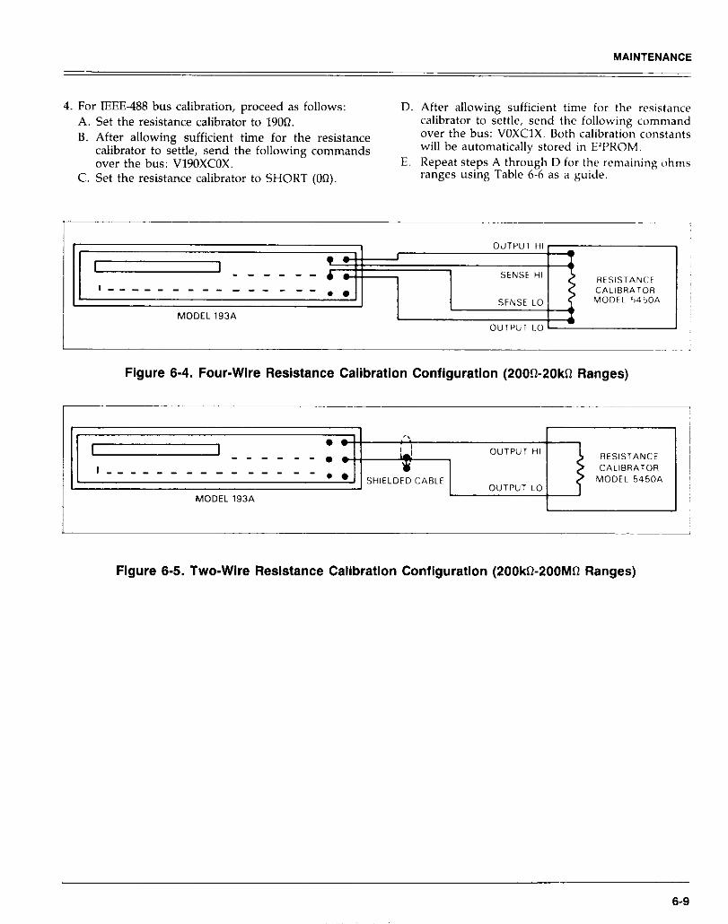
MAINTENANCE
4. For IEEE488 bus calibration, proceed as follows: D. After allowing sufficient time for the resistance A. Set the resistance calibrator to 1900. B. After allowing sufficient time for the resistance
calibrator to settle, send the following commands over the bus: V19OXCOX.
C. Set the resistance calibrator to SHORT (On).
calibrator to settle, send the following command over the bus: VOXClX. Both calibration constants will be automatically stored in E’PROM.
E. Repeat steps A through D for the remaining ohms ranges using Table h-h as a guide.
L
Figure 6-4. Four-Wire Resistance Calibration Configuration (200G20kn Ranges)
Figure 6-5. Two-Wire Resistance Calibration Configuration (200kR-200Mn Ranges)
6-9

MAINTENANCE
Table 6-6. Resistance Calibration
1 l93A Range
200 0
2 kQ
20 kO
200 kR
2MR
ZOMR
200Mll
Set-Up
Figure 6-4
Figure 6-4
Figure 6-4
Figure 6-5
Figure 6-5
Figure 6-5
)pen Inpu
193A Calibration Point
190.0000 n 000.0000 R 1.900000 kO 0.000000 kO 19.00000 kO 00.00000 kR 190.0000 kG 000.0000 kfl 1.900000MQ O.OOOOOOM~ 19.0000OM~ OO.OOOOOMdl Open Input
<esistance Calibrator Setting
39on Short (On)
l.YkO Short (On)
19kQ Short (00)
190kn Short (00)
1.9MQ Short (On)
19Mn Short (On)
Open
IEEE-488 <us Commands
v19oxcox VOXClX
V1.9E3XCOX VOXClX
V19E3XCOX VOXClX
V190E3XCOX VOXClX
V1.9E6XCOX VOXClX
VlYEbXCOX VOXClX
cox
NOTE: The 20Mn range must be calibrated before the 200Mfl range.
6.6.10 TRMS AC Volts Calibration
A full calibration of the ACV function includes four inter- nal, manual adjustments. However, if input offset and high frequency are checked and found to be within the specifica- tions, then the internal adjustments will not have to be done. The following procedure includes these checks. The flowchart in Figure 6-6 helps clarify the calibration procedure.
NOTE For front panel calibration, omit step 6 of the following procedure. For IEEE-488 bus calibration, omit step 5.
1. Input Offset Check: A. Select the ACV function, AC + DC modifier, 5Yzd
resolution and autorange.
NOTE If the 2VDC range is way out of calibration, the messaye “NO OPTION” may be disulaved when the A?V function is selected. To’ rdsolve the problem:
1. Calibrate the 2VDC range. 2. Cycle power on the instrument 3. Repeat step A.
B. Connect the DC calibrator to the instrument as shown in Figure 6-2.
C. Set the DC calibrator to output +l.OOOOOOV. D. Allow the measurement sufficient time to settle and
note the reading on the display of the Model 193A. E. Reverse the leads at the input of the instrument,
allow the measurement to settle and note the reading on the display of the Model 193A.
F. If there is 210 count change between the readings, the input offset is within specification and need not be adjusted, therefore, omit step 2. If there is 210 count change, the input offset is too high and needs to be adjusted. Proceed to step 2.
2. Input Offset Adjustment: A. With the instrument off, disconnect the line cord and
all other equipment from the Model 193A. B. Remove the two screws securing the top cover to
the chassis and slide the the cover back far enough to gain access to the Model 1930.
C. Connect the line cord and power-up the Model 193A.
D. Select the ACV function, AC + DC modifier, 5%d resolution and autorange.
E. Connect the DC calibrator to the instrument as shown in Figure 6-2.
F. Set the DC calibrator to output +l.OOOOOOV. G. After allowing the measurement sufficient time to
settle, adjust the DC calibrator until the display of the Model 193A reads l.OOOOOV *lo counts.
6-10

MAINTENANCE
Figure 6-6. Flowchart of AC Volts Calibration Procedure
H. Reverse the leads at the input of the instrument, allow the measurement to settle and note the reading on the display.
I. Adjust R411 for a display reading that is the average of the two noted readin s. For exam
a i le, if the reading
in step H is 1.004oOV, t en adjust 411 for a display reading of 1.002OOV
J, Repeat steps F through I until there is ~10 counts change between the two readings.
K. Slide the top cover forward to help maintain internal temperatures, but do not replace the screws at this time.
3. Select the ACV function and the 2V range. Take the in- strument out of AC + DC, if it is in that mode.
4. Connect the AC calibrator as shown in Figure 6-8. 5. For front panel calibration, select Program 96 as ex-
plained in paragraph 6.6.5, step 3 and proceed as follows: A. With the 2.OOOOOOV AC calibration point displayed on
the Model 193A, set the AC calibrator to output 2.OOOOOV at 500Hz.
B. After allowing sufficient time for the calibrator voltage to settle, press the ENTER button. The following message will be displayed for several seconds.
CALIBRATING
C. With the 0.2OOOOOVAC calibration point displayed, set the AC calibrator to output .2OOOGGV at 5oOHz.
D. After allowing the calibrator voltage to settle, press the ENTER button. The following message will be displayed for several seconds:
CALIBRATING
E. The instrument will exit the calibration program and return to the 2V AC range.
F. Repeat the procedures in step 5 for the remaining ACV ranges using Table 6-7 as a guide.
6. For IEEE488 bus calibration, proceed as follows: A. Set the AC voltage calibrator to output 2.OooOOV at
500Hz. B. After allowin
to settle, sen 2 sufficient time for the calibrator voltage the following commands over the bus:
v2xcox. C. Set the AC calibrator to output 2OOOOOV at 5C0Hz. D. After allowing sufficient time for the calibrator voltage
to settle, send the followin command over the bus: V20E-3XClX. Both call ratmn constants will .% automatically be stored in E’PROM.
E. Repeat steps A through D for the remaining ACV ranges using Table 6-7 as a guide.
6-11

MAINTENANCE
7. High Frequency Check (100kHz): D. After allowing sufficient time for the measurement A. With the ACV function, autorange and 5%d resolu- to settle, use an insulated alignment tool to adjust
tion selected, connect the AC calibrator to the instru- C413 (see Figure 6-7) for a display reading of ment as shown in Figure 6-8. lOO.OOOV *250 counts.
B. Set the AC calibrator to output lOO.OOOV at a fre- E. Set the AC calibrator to output LOOOOOV at 100kHz quency of 1OOkHz and allow sufficient time for the and set the Model 193A to the 2V range. measurement to settle. F. After allowing the measurement to settle, adjust
C. If the reading is not lOO.OOOV i1500 counts, then C402 for a display reading of LOOOOOV +50 counts. omit steps D through G and proceed to step 8. G. Set the Model 193A to the 20V range and set the AC
D. Set the AC calibrator to output l.OOOOOV at 100kHz calibrator to output lO.OOOOV at 100kHz. and allow the measurement to settle. H. After allowing the measurement to settle, adjust
E. If the reading is not l.OOOOOV f 1500 counts, then C412 for a display reading of lO.OOOOV -t 100 counts. omit steps F and G and proceed to step 8. I. Repeat steps C through H until no other adjustments
F. Set the AC calibrator to output lO.OOOOV at 1OOkHz need to be made. and allow the measurement to settle. J, Turn the Model 193A off, disconnect the line cord
G. If the reading is not lO.OOOOV *1500 counts, then and test cables and fasten the top cover to the chassis. high frequency will have to be adjusted as explained in the following procedure (step 8). If the high fre- quency readings were within the defined range, step 8 does not have to be performed and ACV calibra- tion is completed.
8. High Frequency Adjustment: A. Slide the top cover back to gain access to the Model
1930. If the top cover is fastened to the chassis, per- form steps 2A, 28 and 2C.
B. With the ACV function and 5%d resolution selected, connect the AC calibrator to the instrument as shown in Figure 6-8.
C. Set the Model 193A to the 1OOV range and set the AC calibrator to output 1OO.OtMV at a frequency of 100kHz.
1
WARNING Some procedures require the use of high voltage. Take care to prevent contact with live circuits which could cause electrical shock resulting in injury or death. The shield on the analog board is at input low potential and may have up to 500V on it. Use an insulated align- ment tool to make the following adjustments.
Figure 6-7. TRMS AC Volts Calibration Adjustments
6-12

Table 6-7. TRMS AC Volts (Model 1930) Callbration
193A ACV 193A Calibration AC Calibrator Voltage IEEE-488 Range Point Setting @ 500Hz Bus Commands
I I I !
2 v 2.000000 v 2.00000 v v2xcox 0.200000 v .200000 v VZOOE-3XClX
20 v 20.00000 v 20.0000 v v2oxcox 2.00000 v 2.00000 v V2XClX
200 v 200.0000 v 200.000 v v2ooxcox 20.0000 v 20.0000 v V2OXClX
I :
1000 v 650.000 V 650.000 V V65OXCOX 100.000 v 100.000 v v100xc1x j
HI 1
.
- - - - - - - : . I
POveR , AC “ClLTPiCE
I - - - - - - - - - - - - - - - . . LO AMPLlFiER CALisRnTcm MODEL 52 ISA 1 MODEL 52OOA
MODEL 193.4 I
1
Figure 6-6. TRMS AC Volts Calibration Configuration
6.6.11 DC Current Calibration
With the Model 1931 installed, perform the following pro- cedure to calibrate DCA:
NOTE For front panel calibration, omit step 4 of the following procedure. For IEEE-468 bus calibration, omit step 3.
1. Select the DCA function and the 200,A range. 2. Connect the DC current calibrator to the instrument as
shown in Figure 6-9. 3. For front panel calibration, enter Program 96 as ex-
PolloWS: lained in paragraph 6.6.5, step 3 and proceed as
A. With the 200,OOOO~A DC calibration point displayed on the Model 193A, set the current calibrator to out- put +200.000~A.
B. After allowing sufficient time for the measurement to settle, press the ENTER button. The following message will be displayed for several seconds:
CALIBRATING
C. With theOOO.OOOOFA DC calibration point displayed, set the current calibrator to output 000.00&A.
D. After allowing sufficient time for the measurement to settle, press the ENTER button. The following message will be displayed for several seconds:
CALIBRATING
E. The instrument will exit the calibration program and return to the 200fiA range.
F. Re eat the procedures in step 3 for the remaining D P A ranges using Table 6-8 as a guide.
4. For IEEE-488 bus calibration, proceed as follows: A. Set the current calibrator to output 200.000pA. B. After allowinp. sufficient time for the calibrator current
to settle, send the following command over the bus: V200E-6XCOX.
C. Set the current calibrator to output 000.0OO~A. D. After allowing sufficient time for the calibrator cur-
rent to settle, send the following command over the bus: VOXCIX. Both calibration constants v.?ll auk- matically be stored in E’I’ROM.
E. Repeat steps A through D for the remaining DCA ranges using Table 6-8 as a guide.
6-l 3

Table 6-6. DC Current Calibration
193A DCA 193A Calibration Range Point
200 &A
2m.4
2OIllA
200mA
2 A
2.oooooomA 0.000000mA
200.0000 PA
20.00000mA
000.0000 PA
00.00000mA
2oo.oooomA ooo.oooomA 2.000000 A 0.000000 A
2.00000mA o.ooooom.4 2o.oooomA OO.OOOOmA
2oo.ooomA ooo.ooomA
2ooo.oomA OOOO.OOmA
IEEE-488 Bus Commands
V200E-6XCOX VOXClX
V2E-3XCOX VOXClX
V20E-3XCOX VOXClX
V200E-3XCOX VOXClX v2xcox VOXClX
I I . .
LO OUTPUT LO INPUT LO ------. CURRENT DC VOLTAGE CALIBRATOR CALIBRATOR - - - - - - - - - - - - - - - .
HI OUTPUT MODEL 2500E HI iNPUT HI MODEL 5440A
MODEL 193.4
Figure 6-9. DC Current Calibration Configuration
6.6.12 TRMS AC Current Calibration
With both the Models 1930 and 1931 installed, perform the following procedure to calibrate the ACA function:
NOTE For front panel calibration, omit step 4 of the following procedure. For IEEE-488 bus calibration, omit step 3.
1. Select the ACA function and the 200hA range. 2. Connect the AC current calibrator to the instrument as
shown in Figure 6-10. 3. For front panel calibration, enter Program 96 as ex-
plained in paragraph 6.6.5, step 3 and proceed as follows: A. With the 200.0000pA AC calibration point displayed
on the Model 193A, set the current calibrator to out- put 200.000pA at a frequency of 1kHz.
B. After waiting sufficient time for the measurement to settle, press the ENTER button. The following message will be displayed for several seconds:
CALIBRATING
C. With the OOO.OOOO~A AC calibration point displayed, set the current calibrator to output OOO.OOO~A at 1kHz.
D. After allowing the measurement to settle, press the ENTER button. The following message will be displayed for several seconds:
CALIBRATING
E. The instrument will exit the calibration program and return to the 200~A range.
F. Re A P
eat the procedures in step 3 for the remaining A ranges using Table 6-9 as a guide.
4. For IEEE-488 bus calibration, proceed as follows: A. Set the current calibrator to output 200.000pA at
1kHZ. B. After allowing sufficient time for the calibrator cur-
rent to settle, send the following command over the bus: V2MlE-6XCOX.
C. Set the current calibrator to output OOO.OOOpA at 1kHz.
D. After allowing sufficient time for the calibrator cur- rent to settle, send the following command over the bus: VOXClX. Both calibration constants will automatically be stored in E’PROM.
E. Repeat steps A through D for the remaining ACA ranges using Table 6-9 as a guide.
6-14

MAINTENANCE
Table 6-9. TRMS AC Current Calibration
193A Calibration Current Calibrator Point output @ lkH2
I
200.0000 PA 020.0000 /GA 2.oooooomA 0.200000mA 2o.ooooomA 02.00000nlA 2oo.oooomA 020.0000mA 2.000000 A 0.200000 A
200.000 PA 020.000 IA Z.OOOOOmA 0.20000mA 2o.oooomA 02.0000mA 2oo.ooomA 020.000mA 2000.00mA 0200.00mA
V2KIE-6XCOX V20E-6XClX VZE-3XCOX
V200E-6XClX V20E-3XCOX V2E-3XClX
V200E-3XCOX V20E-3XClX
Figure 6-10. TRMS AC Current Calibration Configuration
6.7 DISASSEMBLY INSTRUCTIONS C. Slide the bottom cover towards the rear until it com- pletely separates from the chassis.
If it is necessary to troubleshoot the instrument or to replace 3. Remove the analog board as follows: a component, use the following disassembly procedure. A. The top shield is snugly secured to the analog board Refer to Figures 6-11 and 6-12. by four retaining clips. Remove the top shield by
carefully lifting it up and off the analog board.
WARNING Disconnect the line cord and any test leads from the instrument before disassembly.
1. Remove the top cover as follows: A. The top cover is secured to the chassis of the Model
193A by two screws located at the rear of the instru- ment. Remove those two screws.
8. Slide the top cover towards the rear of the instrument until it completely separates from the chassis.
2. Remove the bottom cover as follows: A. If installed, remove the four plastic feet located on
the bottom cover. They are secured with four screws. 8. The bottom cover is secured to the chassis of the
Model 193A by two screws located at the rear of the instrument. Remove those two screws.
CAUTION Take care not to contaminate components or the circuit board by touching , as thls could adverse- ly effect Instrument performance.
B. Disconnect the input wires from both the front and rear panel input terminals.
C. Disconnect I’/] 1016 which is a six pin connector (five pins used).
D. Disconnect and remove the wires that feed through the four pulse transformers. When reinstalling, make sure that the wires are fed through the transformer cores in the correct direction as shown by the arrows etched on the PC-board and in Figure 6-11.
6-l 5

E. From the bottom, remove the five screws that secure the analog board assembly to the mounting rails. Carefully remove the analog board from the instru- ment case taking care not to touch the PC board sur- faces or any components.
F. The bottom shield is secured to the analog board by two screws accessible from the component side of the board. Again, be careful not to touch the PC board surfaces or any components when removing the shield.
4. Remove the digital board as follows: A.Disconnect the display board ribbon cable (P/J 1017),
located near the front of the instrument, from the digital board.
B. Disconnect the EXTERNAL TRIGGER In ut and VOLTMETER COMPLETE wirine harness f If /I 1015).
C. Place the Model 193A on its side and remove the six screws securing the digital board to the mounting rails. The screws are accessible from the bottom.
D.Now place the instrument right-side up and remove the two screws securing the IEEE-488 connector to the rear panel.
E. Remove the four screws seculing the rear panel to the chassis.
F. Remove the rear panel. T a
reen, powerline ground wire from the e ground wire is secured to the panel
with a pem nut. G.Place the rear panel in a location that is clear of the
digital board. H.Carefully lift the digital board out of the instrument.
5. Remove the display board as follows: A.Remove each of the four decorative strips from the
side panels as follows:
1. Place a thin blade screwdriver into one of the holes where the decorative strip is secured.
2. Carefully push outwards until the strip disengages from one of the fasteners.
3. Pull the strip away from the side panel.
Note: To reinstall, align the strip in the recessed part of the side panel and then press the strip at the locations of the fasteners.
B. Remove the four screws that secure the front panel assembly to the side panels and disengage the front panel assembly from the chassis.
C. Loosen the four Allen set screws securing the bezel assemblies to the front panel. Remove the bezel assemblies from the front panel.
D. Lift the display board assembly from the front panel. E. To separate the jumper board from the display board,
disconnect the display ribbon cable at the display board and remove the two retaining screws that are accessible from the component side of the displav board.
6. The instrument can be reassembled by reversing the above procedure. Make sure that all parts are orooerlv seated and secured and that all conn&tions are proper- ly made. To ensure proper operation, shields must be re- placed and fastened securely.
WARNING To ensure continued protection against safety hazards, power line ground (the green wire at- tached to the AC power receptacle) must be connected to the rear panel.
6.16

MAINTENANCE
i
Figure 6-I 1. Connectors
6-17/6-16


MAINTENANCE
2@7- DECORbTlVE STRIP 14,
Figure 6-12. Model 193A Exploded View
6-19/G20

MAINTENANCE
6.6 SPECIAL HANDLING OF STATIC- SENSITIVE DEVICES
CMOS devices operate at very high impedance levels for low buil x
ower consumption. As a result, any static charge that s up on your person or clothing may be sufficient to
destroy these devices, if they are not handled properly. Table 6-10 lists static-sensitive devices used in the Model 193A. When handling these devices, use the following pre- cautions to avoid damaging them.
1. The devices listed in the table should be transported and handled only in containers specially designed to prevent static build-up. qpically, these parts will be received in anti-static containers of plastic or foam. Keep these devices in their original containers until ready for install- ation.
2. Remove the devices from their protective containers only at a properly grounded work station. Also ground your- self with a suitable wrist strap.
3. Handle the devices only by the body; do not touch the pins.
4. Any printed circuit board into which the device is to be inserted must also be grounded to the bench or table.
5. Use only anti-static type solder suckers. 6. Use only grounded tip solder irons. 7. Once the device is installed on the PC board, it is nor-
mally adequately protected and normal handling can resume.
6.9 TROUBLESHOOTING
The troubleshooting information contained in this section is intended for use by qualified personnel having a basic understanding of analog and digital circuitry. The indi- vidual should also be experienced at using typical test equipment as well as ordinary troubleshooting procedures. The information resented here has been written to assist in isolating a de ectwe clrcult or crcud section. Isolation
p...
of the specific component is left to the technician. Note that schematic diagrams and component location drawings, which are an essential aid in troubleshooting, are located at the end of Section 7.
Table 6-10. Static-Sensitive Devices
Circuit Designation Keithley Part No. Model 193A
QlOl TG-175 4106 TG-175 QlO8 TG-128 Qlll TG-128 4112 l-G-l39
QlBQll5 TG-128 Q116-Qll8 TG-I39
Q119 TG-128 QL?O-Q143 TG-139
u104 IC-413 U106 IC-412 U118 IC-135 u119 IC-283
ulzo, ul21 K-337 ul22 IC-343 u123 lC-351 ul24 IC-417
U125, Ul26 IC-416 ul27 IC-3X%47-1 U128 IC-337 ul29 K-414 u301 IC-98 U302 IC-179 u303 IC-190 u304 IC-398 u305 lC-399 U306 IC-186 u307 IC-182 u309 IC-397 u3l2 LSI-67 U318 IC-397 u319 lC-2l3 U320 IC-351 U321 IC-177 U323 IC-173 U402 IC-141
Model 1930 Q402 TG-84
4404-4408 TG-128 Model 1931
u102 lC-206 u103 IC-251
6-21

6.9.1 Recommended Test Equipment
Success in troubleshooting complex equipment like the Model 193A depends not only on the skill of the techni- cian, but relies on the use of accurate, reliable test e ui - ment. Table 6-11 lists the equipment recommende % fzr troubleshooting the Model 193A. Other equipment such as logic analyzers and capacitance meters could also be helpful especially in difficult situations.
6.9.2 Power-Up Self Test
Upon power-up, the instrument will do a number of tests on itself. Tests are performed on memory (ROM, RAM and E2PROM). Whenever one of the memory tests fails, the inshument will lock up and must be repaired. Imme- diatelyafterturningon theMode 193A, thefollowingse- quence will take place:
1. A digital check will be performed on the ROM circuitry. If the test fails, the instrument will lock up with the following message displayed:
00000000000000
function.
Replacing U314 and U315 may resolve the problem. 2. If the ROM test passes, a digital self-test will then be per-
formed on the RAM circuitry. If the RAM test fails, the instrument will lock up with the following error message displayed:
AAAAAAAAAAAAAA
Replacing U3l3 may resolve the problem. 3. Finally, the E2PROM circuitry where the calibration con-
stants, IEEE address and line frequency settings are stored will be checked. If this test fails, the following message displayed:
UNCALIBRATED
Pressing any front panel momentary button will return the instrument to normal operation however, a complete calibration will have to be performed, and the IEEE ad- dress and line frequency setting should be checked. If the test still fails after calibration, try replacing U3l2 before recalibrating the instrument again.
4. The instrument will then RO to the power-up default
Table 6-11. Recommended Troubleshooting Equipment
Equipment 1 Use I
Five function DMM with 0.1% basic DCV accuracy, 1OM input impedance.
Power supply and DC voltage checks; analog signal tracing continuity, logic levels.
Dual-trace, triggered sweep oscilloscope, DC to 50MHz.
Digital and analog waveform checks.
Digital Frequency Counter Checking clock frequencies.
6-22

MAINTENANCE
6.9.3 Program 93 - Self Diagnostic Program
This front panel program performs a display test and the same memory tests performed upon power-up. Also in- cluded is a troubleshooting test mode, that is designed to switch on various switching FETs and relays to allow signal tracing through the instrument. Perform the following pro- cedure to utilize Program 93:
1. Press the PRGM button and then the 9 and 3 buttons. First is the dis lay test. All segments of the display characters and ront panel LEDs will be simultaneously P displayed for a short period of time. This test allows the operator to note inoperative display segments of LEDs. Self test on the ROM, RAM, and E’PROM will then be performed. These are the same tests run on power-up and are explained in detail in paragraph 6.92.
2. The Model 193A will now go into the troubleshooting mode with the first N mode being displayed as follows:
N 01
The instrument is still on the same function and range as it was before Program 93 was run.
3. Using Table 6-12, reference the N mode to the current function and range to determine the proper working status of the listed circuit components.
4. To change the N mode, use the TRIGGER button. 5. To troubleshoot a different function and/or range, exit
the program by pressing any fmnt panel momentary but- ton (except TRIGGER), select the desired function andior range and again run Program 93.
6.9.4 Power Supplies
Table 6-13 shows the various checks that can be made to the power supplies of the Model 193A. In addition to the normal voltage checks, it is a good idea to check the various supplies with an oscilloscope for signs of noise or oscillations.
6.9.5 Signal Conditioning Checks
These circuits can be checked by using the diagnostic pro- gram (Program 93) as explained in the paragraph 6.9.3.
6.9.6 Digital and Display Circuitry Checks
The digital and display circuitry can be checked out by us- ing the troubleshooting data found in Tables 6-14 and 6-35.
6-23
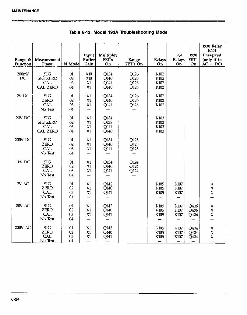
Table 6-12. Model 193A Troubleshooting Mode
Range & Functior
2oomv DC
2V DC
20V DC
200V DC
ZkV DC
2V AC
20V AC
200V AC
Measurement Phase
SIG SIG ZERO
CAL CAL ZERO
SIG ZERO CAL
No Test
SIG SIG ZERO
CAL CAL ZERO
SIG ZERO CAL
No Test
SIG ZERO CAL
No Test
SIG ZERO CAL
No Test
SIG ZERO CAL
No Test
SIG ZERO CAL
No Test
t N Mod{
ii 03 04
01
:: 04
01 02 03 04
01 02 03 04
i: 03 04
:; 03 04
ii
ii
01
ii 04
Inpul Multiplex Buffe FFTS Gain 0”
x10 x10 Xl Xl
Xl Xl Xl -
Xl Xl Xl Xl
Xl Xl Xl -
Xl Xl Xl -
Xl Xl Xl -
Xl Xl Xl -
Xl Xl Xl -
0,:: Q141 Q140
Q134 Q140 Q141
-
Q134
TjE Q140
Q134 4125 Q140 Q=5 4141 QU
- -
gi: 8% Q141 Q124
- -
:::i 4141
-
4142 K105 4140 K105 Q141 K105
- -
Q142
“,E -
Range R&J? FET’s 0” 0”
t$z Ql26 Q126
Ql26 Ql26 Ql26
-
K102 K102 K102 K102
K102 K102 K102
-
K103 K103 K103 K103
1931 1930 Relay FET’!
0” 0”
K105 K107 K105 K107 K105 K107
- -
KW K107 K107 -
K105 K107 K105 K107 K105 K107
g: Q40f
-
Q404
1930 Iz K40
Energi (only i 4c +
:: X -
X X X -
E X
6-24

MAINTENANCE
Table 6-12. Model 193A Troubleshooting Mode (Cont.)
-
Range &I Function
700V AC
2000
2k0
20kdl
200kfl
2Mbl
20MCl
SIG ZERO CAL
No Test
REF HI REF LO
SENSE HI SENSE LO
REF HI REF Lo
SENSE HI SENSE Lo
REF HI REF LO
SENSE HI SENSE LO
REF HI REFIX)
SENSE HI SENSE LO
REF HI
SENSE HI
SENSE LO
No Test
REF HI SENSE HI SENSE Lo
No Test
REF HI SENSE HI SENSE LO
No Test
P J Mode
01 02
it
01 02 03 04
01 02 03 04
01 02 03 04
01 02 03 04
01
02
03
04
01 02 03 04
01 02 03 04
Inpui Multiplex Buffe FET’S G&l Oil
Xl Xl Xl -
Xl Xl x10 x10
Xl Xl Xl Xl
Xl Xl Xl Xl
;: Xl Xl
Xl
Xl
Xl
Xl Xl Xl
Xl Xl Xl .-
Q142 Q140 Q141
-
Ql25,QL’S QWQn4 QWQU4 QI25,Ql.T
Ql25,Ql.S
QWQ134
QI25,QI.Y
-
Ql25,QI.X QI25,QEP Q125,Ql35
-
( (
: ( 1 (
( (
: ( 1 (
’ I I
I I 1 ,
’ ( (
L ( t I
I
I
I
I I
T
I 3
Range R&p FET’S On On
K105 K107 K105 KW7 K105 KlCV
<lOl, K102 <lOl, K102 <lOl, K102 <lOl,KlOZ
>ll5,QllS,Ql: Jll5,QllB,Qr ~ll5,QllE,Ql: >115,Q118,Ql:
<lOl,KlOZ ;<lOl,KlOZ KlOl, K102 KlOl,KlOZ
>114,Qll7,Ql: ~114,Q117,Ql: 2114,QllZQl: Lj114,Qll~Qr
KlOl, K102 KlOl, K102 KlOl, K102 KlOl, K102
KlOl,KlOZ KlOl,K102 KlOl,KlOZ KlOl, K102
Q1%iur Q116,QllZ
Q119 Q116,Qll2
Qll9 -
L9 1 19 1 19 1 19 1
19 I 19 1 19 1 19 1
19 1 19 1 19 1 19 1
19 I 19 I 19 I 19 1
1
1
I
KlOl, K102
KlOl, K102
KlOl,KlOZ
Q116,Qlll Qll6,Qlll Qll6,Qlll
-
KlOl, K102 KlOl, K102 KlOl, K102
Q116,Qlll KlOl Q116,Qlll KlOl Q116,Qlll K701
1931 Z&p
Oil
1930 Relay K401
Energized :onIy if in IC + DC)
X X X
6-25

Table 6-12. Model 193A Troubleshooting Mode (Cont.)
Range 8
Function
ZOOpA AC
2mA A(
2omA AC
ZOOmA AC
2A AC
zoo/LA DC
r 1
1
M‘%XSlWXNl Phase
SIG
ZERO
CAL
No Test
SIG
ZERO
CAL
No Test
SIG
ZERO
CAL
No Test
SIG
ZERO
CAL
No Test
SIG
ZERO
CAL
No Test
SIG SIG ZERO
CAL CAL ZERO
t V Mode
01
02
03
04
01
02
03
04
01
02
03
04
01
02
03
04
01
02
03
04
01 02
Input Buffer Gain
Xl
Xl
Xl
-
Xl
Xl
Xl
-
Xl
Xl
Xl
-
Xl
Xl
Xl
-
Xl
Xl
X
-
x10 x10 Xl Xl
I Multiple> PET’S Oil
Q142
Q140
Q141
-
Q142
Q140
4141
-
4142
4140
4141
-
4142
Q140
Q141
-
Q142
Q140
Q141
-
4143
gi: Q140
Range FITS On
RAYS Oil
1931 Relayr
On
K106, KlOl K106, KlOl K106, KlOl
-
K106, K102 K106, K102 K106, K102
K106, K103 K106, K103 K106, K103
-
K106, K104 K106, K104 K106, K104
-
K106, K105 K106, K105 K106, K105
-
KlOl KlOl KlOl KlOl
1930 ;ET’s On
1930 Relay K401
Energized (only if in AC + DC)
- -
6.26

MAINTENANCE
Table 6-12. Model 193A Troubleshooting Mode (Cont.)
Range & Fun&or
2mA DC
2omA DC
ZOOmA DC
2ADC
Q143 Q141 Qlm Q143
CAL 03 Xl CALZERO 04 Xl
SIG 01 x10 Q143 SIG ZERO 02 x10 Q140
CAL 03 Xl 4141 CALZERO 04 Xl Q140
SIG 01 x10 SIG ZERO x10
CAL i: Xl CALZERO 04 Xl
4143 Q140 Q141 Q140
R&p OXl
1930 Relay K401
1931 1930 Energized Relays FET’s (only if in
On On AC + DC)
K102 K102 K102 K102
K103 K103 i K103 1 K103
K104 K104 K104 K104
K105
6-27

MAINTENANCE
Table 6-13. Power Supply Checks
step ItemlComponent Required Condition Remarks
1 S302 Line Switch Set to 115 or 230V as required. Line voltage selection. 2 F301 Line Fuse Check for continuity. Remove fuse to check. 3 Line Power Plugged into live receptacle;
power on. 4 +5V Digital Supply U301, pin 2 +5V, *5% Referenced to digital common. 5 +5V Analog Supply VR301, pin 2 +5v, *5% Reference to analog common. 6 +15V Analog Supplies VR302, pin 2; +15V, -15V, +0.75V
VR303, pin 2 Referenced to analog common
Table 6-14. Digital Circuitry Checks
step Item/Component Required Condition ReIILWk.9
1 u3I2, u3l.3, u314, u315 Pass RAM, ROM and EPROM (RAM or ROM) self-test on power up.
Display will lock if failure occurs.
2 U310, pin 2 (PAO) 3 U310, pin 3 @‘Al)
TTL level pulses every lmsec. VIA clock TTL level pulses every 15msec Data
4 U310, pin 6 (PA4) Switch data (+5V or OV) 5 U310, pin 7 (IX5)
Data input to VIA Switch data (+5V or OV)
6 U310, pin 8 (PA6) Data input to VIA
Switch data (+5V or OV) 7 U310, pin 9 (PA7)
Data input to VIA
8 U310, pin 19 Switch data (+5V or OV) Variable pulse train (OV to +5V)
Data input to VIA VIA Data Line
9 U320, pin 6 Variable pulse train (OV to +5V) 10 U106, pin 13 Variable pulse train (OV to +5V)
Data Output
11 U310, pins 12 through 16 Output of A/D Converter
Variable pulse train (OV to +5V) 12 U311, pin 3
Analog data to VIA IRQ line
l3 U311, pin 37 lkHz pulses +5v, *5% Reset line
14 U3l6, pin 9 +5V signal pulsed OV to +5V INT line e”ery lmsec.
15 U316, pin 19 +5V (Logic “Y’) RESET line 16 U316, pin 18 2MHz square wave at OV to +5v lock 17 U316, pin 28 Should go false (+5V) when ATN line
command is sent. 18 U316, pins 28 (ATN),
24 (NDAC), 25 (NRFD), Refer to Figure 3-2 for required conditions.
Handshake Sequence
26 (DAV), and the data lines.
6-28
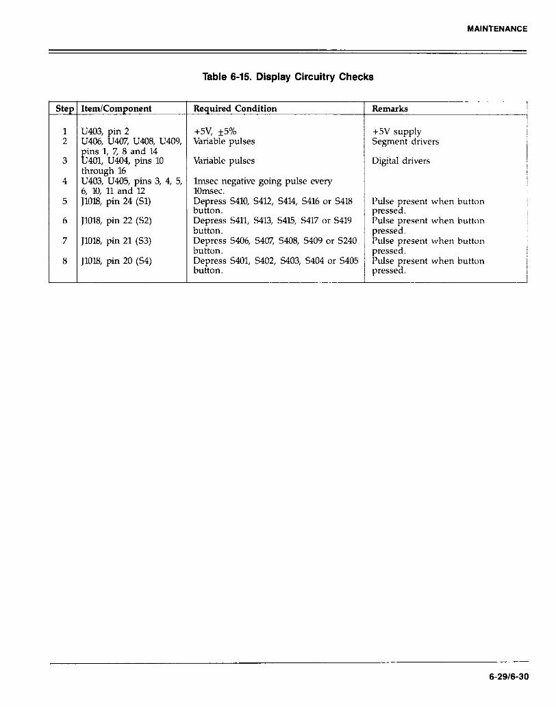
MAINTENANCE
Table 6-15. Display Circuitry Checks
step Itemlcomponent Required Condition RGXLXk9
1 U403, pin 2 +5V, *5% U406, U407, U408, U409, Variable pulses
j ~gl~~~~ ys”lo
+5v supply Segment drivers
throigh 16 ’ Variable pulses Digital drivers
4 u403, u405, pins 3, 4, 5, lmsec negative going pulse every 6, 10, 11 and 12 10msec.
5 JlOl8, pin 24 (Sl) Depress 5410, 5412, 5414, 5416 or 5418 button.
Pulse present when button pressed.
6 JlOZ3, pin 22 (52) Depress 5411, 5413, 5415, 5417 or 5419 Pulse present when button button. pressed.
7 JlOl8, pin 21 (53) Depress 5406, 5407, S408, 5409 or 5240 Puke present when button button. pressed.
8 JlOl8, pin 20 (54) Depress 5401, 5402, 5403, 5404 or 5405 Pulse present when button button. pressed.
-
6-29/6-30


SECTION 7 REPLACEABLE PARTS
7.1 INTRODUCTION
This section contains replacement parts information, com- ponent location drawings and schematic diagrams for the Model 193A.
7.2 PARTS LIST
Parts are listed alphanumerically in order of their circuit designations. Table 7-l contains parts list information for the display board. Table 7-2 contains parts list information for the digital board. Table 7-3 contains parts list informa- tion for the analog board. A parts list for the Model 1930 option is contained in Table 7-4; while Table 7-5 contains a parts list for the Model 1931 option. Table 7-6 contains a mechanical parts list for the Model 193A.
7.3 ORDERING INFORMATION
To place an order, or to obtain information concerning replacement parts, contact your Keithley representative or the factory See inside front cover for addresses. When ordering include the following information:
1. Instrument Model Number 2. Instrument Serial Number 3. Parts Description 4. Circuit Designation (if applicable) 5. Keithley Part Number
If an additional instruction manual is required. order the manual package (Keithley Part Number 193-901-00). The manual package contains an instruction manual and am applicable addenda.
7.4 FACTORY SERVICE
If the instrument is to be returned to the factory for ser- vice, please complete the service form which follows this section and return it with the instrument.
7.5 SCHEMATIC DIAGRAMS AND COMPONENT LOCATION DRAWINGS
Schematic diagrams and component location drawings follow the a ticular boar s
propriate replaceable parts list for that par-

REPLACEABLEPARTS
Table 7-1. Display Board, Parts List
Circuit Desig.
c401 C402
Description
Capacitor, lOpF, 25V, Aluminum Electrolytic Capacitor, O&F, 5OV, Ceramic Film
Schematic Keithley Location Part No.
D5 c-314-10 c5 C-237-J
SW DD-39 sev PL-7l
CS-362.13 CS-363-13
R401 R402 R403 R404
5401.5420
u401 U402 u403 u404 u405 U406 u407 U408 u409
Resistor, Thick Film Resistor, Thick Film Resistor, Thick Film Resistor, Thick Film
Switch, Pushbutton
Darlington Transistor Array, ULN2003A Hex Inverter, Open Collector Output, CD40l2AE E-Bit Serial-In/Parallel-Out Shift Re ister 74HCTl64 Darlin ton Transistor Array, ULN2 03A
Trans~t~r Array MPQ3906 ” &Bit erlal-In/Parallel-Out Shift Regdx 74HCTl64
Transistor Array: MPQ3906 Transistor Array, MPQ3906 Transistor Array, MPQ3906
SW Sev SW Sev
SW
iii F4
TF-43 TF-43 TF-77 TF-77
SW-435
IC-206 K-141 IC-456 IC-206 IC-456 K-396 IC-396 IC-396 IC-396
7-2

REPLACEABLE PARTS
/ I Figure 7-1. Jumper Board, Component Location Drawing, Dwg. No. 193-160
l-3

REPLACEABLEPARTS
Figure 7-2. Display Board, Component Location Drawing, Dwg. No. 193-110
7-4


REPLACEABLE PARTS
Table 7-2. Digital Board, Parts List
Circuit Desig. Description
BT301 Battery, NiCad, 3.6V
c301 C302
Capacitor, 10,00O~F, 25V, Aluminum Electrolytic Capacitor, 10~ F, 25V, Aluminum Electrolytic
c303 c304
Capacitor, 0.33~ F, 5m, Ceramic Film
c305 Capacitor, 0.1~ F, 5OV, Ceramic Film
S%
Capacitor, 0.1~ F, 5OV, Ceramic Film Capacitor, 0.1~ F, 5OV, Ceramic Film
C308 Capacitor, 0.1~ F, SOV, Ceramic Film Capacitor, 0.1~ F, SOV, Ceramic Film
c309 c310
Capacitor, 0.1~ F, 5OV, Ceramic Film
c311 Capacitor, 0.1~ F, 50V
s;:
Capacitor, 0.01~ F, 5OOV, Ceramic Disc Capacitor, 0.1~ F, 50V Capacitor, 0.1~ F, 50V Capacitor, 0.1~ F, 5OV, Ceramic Film Capacitor, l5pF, lOOOV, Ceramic Disc Capacitor, 15 F, lOOOV, Ceramic Disc
Schematic Keithley Location* Part No.
2lG2 BA-36
2lD2 C-342-10,000 2iE2 c-314-10 2lD2 C-237-.33 l/Al C-237-.1 l/B1 C-237-.1 l/Cl C-237-.1 l/Cl C-237-.1 l/F2 C-237-.1 l/El C-237-.1 l/H3 C-365-.1 l/H3 c-22-.01
Capacitor, 0. p F, 50V 4 Capacitor, 0.1~ F, 50V Capacitor, 0.1~ F, 50V Capacitor, 10~ F, 25V, Aluminum Electrolytic Capacitor, 0.1~ F, 5OV, Ceramic Film Capacitor, 0.1~ F, 5OV, Ceramic Film Capacitor, 10~ F, 25V, Aluminum Electrolytic Capacitor, 0.1~ F, 50V Capacitor, 0.1~ F, 50V Capacitor, 0.1~ F, 5OV Capacitor, 0.1~ F, 5OV, Ceramic Disc Capacitor, 0.1~ F, 50V Capacitor, 0.1~ F, 50V Capac/tor, O&L F, 50V
:‘iii C-365-.1 C-365 I
l/E4 i c-237-.1 l/A5 / C-64.15p
c314 c315 C316 c317 c3l8 c319 C320 C321 C322 C323
% C326
:iz C329
:% l/D6 C-365-.1
:zzt
~oyiibj 0.1~ F, 50V C-365-.1
2 i EEi.? liD4 C-365-. 1 l/C4 C-365-.1 2ic2 c-314-10 l/C4 C-237-.1 1184 C-237-.1 l/Ah c-314-10
:‘125’ C-365-.1 C-365-.1
l/C4 C-365.. I l/A6 c-22-.01 l/G4 C-365.1 l/H2 C-365-.1
c334 Capacitor, 2200~ F, 25V, Aluminum Electrolytic
c335 Capacitor, 10~ F, 25V, Aluminum Electrolytic
:::c
Capacitor, 10~ F, 25V, Aluminum Electrolytic Capacitor, 10~ F, 25V, Aluminum Electrolytic Capacitor, 620~ F, 35V, Electrolytic
C338 c339
Capacitor, 620~ F, 35V, Electrolytic
:z:;
Capacitor, 0.11 F, 50V Capacitor, 0.1~1 F, 50V Capacitor, 0.1~ F, 50V
:E Capacitor, O.lj~ F, 50V Capacitor, 10~ F, 25V, Aluminum Electrolytic
c344 Capacitor, 0.0047~ F, SOOV, Ceramic Disc
CR301 Bridge Rectifier, lA, 1OOPIV CR302 Bridge Rectifjer, 5A, PE05
$i& !%l’b: %%;~l?ki,’ WO4M Diode, Silicon, lN4148
CR306 Diode, Silicon, lN4148 CR307 Diode, Silicon, lN4148
*Page/Zone
2lD3 C-314-2200 2iE3 c-314-10 2iE5 c-314-10 2iEh c-314-10 2lD5 C-309-620 2lD5 C-309-620 l/D6 C-365-.1 l/B5 C-365-.1 l/B5 C-365-.1
% c-365-.1 c-314-10
l/B6 C-22-0047
l/D5 RF-52 2lD2 RF-48 2lD3 RF-48 2iD5 RF46 2iG2 RF28 l/A5 RF28 l/A6 RF-28
7-?

REPLACEABLE PARTS
Table 7-2. Digital Board, Parts List (Cont.)
Circuit Schematic Keithley De&g. Description Location* Part No.
F301 Fuse, %A, 25OV, Slo-Blo, MDL Z./B4 FU-18 F301 Fuse, %A, 25OV, Slo-Blo, 3AG ZIG2 FU-29
JlOl.3 Connector, IEEE l/H2 cs-501
g:t AC Receptacle Z/B5 CS-388
l/D5 cs-339-3 71017 ::iz:::::: 2$s l/G6 (X-389-3
Q301 Translator, NPN, Silicon, 2N3904 2lG2 TG-47 Q302 Translator, PNP, Silicon, 2N3906 Z/G2 TG-84
R301 l/C5 R-76-100 R302
Resistor, 1000, 5%, ‘/aW, Composition Resistor, lOOD, 5%, ‘/aW, Composition l/D5 R-76-100
R303 Resistor, 3.3k0, 5%, ‘/aW, Composition l/D5 R-76.3.3k I7304 Resistor, Thick Film l/A3 TF-140 R305 Resistor, lM0, lo%, ‘/aW, Composition R-76-lM R306 2iF2 R-76-4.7k
iE3
Resistor, 4.7k62, 5%, s/,W, Composition Resistor, 15kR, 5%, ‘/aW, Composition 2iF2 R-76.15k
2lG2 R-76-lk R309
Resistor, lkfl, 5%, ‘/aW, Composition
Rx0 Resistor, 1504 5%, ‘XW, Composition R-76-150
R311 Resistor, 61.9k62, l%, %W, Composition ‘1’12: R-88.61.9k
R312 Resistor, 20k0, l%, %W, Composition l/A6 R-88-20k
EE
Resistor, 26lk0, l%, ZW, Composition l/A6 R-88-261k Not Used Not Used
R3l5 I7316 FE kE R317
EE
Resistor, 4700, 5%, ‘/qW, Composition l/C6 R-76-470 Resistor, lk0, 5%, ‘/aW, Composition l/D6 R-76-l k Resistor, 2.4k0, 5%, ‘hW, Composition l/C6 R-76.2.4k
R320 R321
Resistor, 1000, 5%, ‘/aW, Composition l/C6 R-76-100 l/C6 R-76-47
I7322 Resistor, 47% 5%, ‘/aW, Composition Resistor, 2.2kn, 5%, l/qW, Composition l/D2 R-76.2.2k
R323 R324
Resistor, 82fl, 5%, ‘/aW, Composition l/C5 R-76-82 l/C5 R-76-82
R325 Resistor, 820, 5%, ‘/aW, Composition Resistor, 8262, 5%, ‘/aW, Composition l/C6 R-76-82
s301 Switch 5302 Switch % ~i:~~ s303 Switch l/E6 SW-318
T301 Transformer, USA. 2ic2 TR-210 T301 Transformer, Japan z/c2 TR-233 T302 Pulse Transformer T303 Pulse Transformer :I@ ;;I;:: l-304 Pulse Transformer l/B6 TR-211
u301 U302
5V Regulator, LM309k 2iE2 IC-98 Quad 2-Ingut, Non Gate 74LSO? SW IC-179
u303 Dual 2 to u304
Lme DecoderiMultlplexer, 74LSl.39 l/B1 IC-190 3 to 8 Line Decoder, 74HCTI.38 l/Cl IC-398
u305 C-MOS Quad 2-In U306 Hex Inverter, 74LS l
ut NAND, 74HClTiO Sev IC-399 4 Sev IC-186
u307 l/El IC-182 U308
DecodersiDemultiplexers, 74LSl38 Octal GPIB Transceiver, 7516lA l/H4 IC-299
u309 C-MOS Tri-State Flip-Flop, MM74HCT374 l/F4 IC-397
7-a

REPLACEABLE PARTS
Table 7-2. Digital Board, Parts List
* ;*Order same software as presently installed. For example, if the software revision level is Ch then order 193.800.Ch and 193-801~C6.
Circuit Desig. Description
Schematic Keithley Location* Part No.
u310 u311 U312 u3l3 u314 u315 U316
%E u319 U320 U321 U322 U323
Versatile Interface Ada ter (VIA), 6522A ~~~~~~~~~~~~~~~~~l~C68B09
819 Word x 8 Bit Static CMOS RAM, HM6264LI’.15 16k x 8 UV Erasable PROM, 27128 8k x 8 UV Erasable PROM, 2764 GI’IB Ada ter, 9914A Octal GPI !I Transceiver, 75160A C-MOS Tri-State Flip-Flop, MM74HCI374 Dual 4 Bit Decade and Bmary Counter, 74LS393 Quad 2-Input NAND Gate Microorocessor Bioolar Monolithic IC Not Lffsed 1
111.4 liA4 l!D4 l/C4 liC4 1184 l/G4 l/H3 l/M 106 se\, l!Ah
Voltage Comparator, LM31L4 l.‘Ch
vR301 vR302 vR303 VR304
+5\!,Voltaqe ReTlator, 7805 l’osltwe Vo tage egulator, 78M15CU Negative Voltage Regulator, 79M15CU Voltage Regulator Dmde, Silicon, IN702A
2!E2 IC-Y3 2iE.7 IC-194 2iE4 IC-195 l!C6 DZ-33
MO1 Crvstal. 8MHz l/A5
1%45 LSl-65 LSl-83 LSI-66 193.800” 193.ROl-” LSI-49 g;;
IC-213 IC-351 IC-177
IC--526
CR-24-l
7-9

REPLACEABLE PARTS
6 )
Figure 7-4. Digital Board, Component Location Drawing, Dwg. No. 193-100
7-10

/ _/_/../l, :, ;/ ._/ .%! ../
I c/...“a /“.
I

t
t
-t

REPLACEABLE PARTS
Table 7-3. Analog Board, Parts List
Circuit Desig. Description
Schematic Keithley Location’ Part No.
I I I Cl01
:::i Cl04 Cl05 Cl06 Cl07
EE Cl10 Cl11 Cl12 Cl13
:::z Cl16 Cl17 Cl18 Cl19
SE Cl22 Cl23 cl24 cl25
:t% Cl28 cl29 cl30 cl31
:E cl34 cl35 Cl36 cl37 Cl38 cl.39 Cl40 Cl41 Cl42 Cl43
$2 Cl46 Cl47 Cl48 Cl49
:E Cl52
Capacitor, 0.1~ F, 50V Capacitor, lp F, 5OV, Ceramic Film Capacitor, lp F, 5OV, Ceramic Film Capacitor, l/~ F, 5OV, Ceramic Film Capacitor, l/c F, 5OV, Ceramic Film Capacitor, 0.015~ F, ZOOV, Polycarbonate Capacitor, 0.015~ F, 2OOV, Polycarbonate Ca
I; acitor
No used lOOpF, lOOOV, Ceramic Disc
Not Used Not Used Not Used Not Used Capacitor, 0.1~ F, 50V Capacitor, 0.1~ F, 50V Capacitor, 0.1~ F, 50V Capacitor, 0.1~ F, 50V Capacitor, 0.1~ F, 50V Capacitor, 0.1~ F, 50V Capacitor, 68pF, lOOOV, Ceramic Disc Capacitor, 68pF, lOOOV, Ceramic Disc Capacitor, 47 Capacitor, 47 F, F, lOOOV, Ceramic Disc lOOOV, Ceramic Disc Capacitor, Capacitor, 0. 0. f f p F, 50V p F, 50V Capacitor, 0.1~ F, 50V Capacitor, 0.1~ F, 50V Canaritnr II 1~ E .5lW Capacitor, 0.1~ F, 50V
I Capacitor, .lOy. F, 25V, Aluminum Electrolytic Capacitor, 0.1~ F, 50V
: Capacitor, 0.1~ F, 50V Capacitor, 15
I Capacitor, 0. CT
F, lOOOV, Ceramic Disc 047~ F, lOOV, Metalized Polypropyl~
Capacitor, O.lb F, 50V ( Capacitor, 0.1~ F, 50V
I Capacitor, l/~ F, SW, Ceramic Film Capacitor, 0.1~ F, 50V ( Capacitor, 1~ F, 5OV, Ceramic Film Cavacmx “.lU I., SW Cauacitor. 0.1~ F, 50V Capacitor Capacitor, Capacitor, Not Used Capacitor, Not Used Capacitor, Capacitor, Capacitor, Capacitor, Capacitor, Capacitor, Not Used Capacitor, Capacitor, Not Used Capacitor, Capacitor, Capacitor, Capacitor, Capacitor, Capacitor,
0.1; I+, 5ov O.lp F, 50V 10~ F, 25V, Aluminum Electrolytic
22OpF, 5OOV, Polystyrene
150 82 p:
E 5OOV, Polystyrene 1OOOV Ceramic Disc
l&O’ F lOOh, Ceramic Disc O.lp %,;OV
10~ F, 25V, Aluminum Electrolytic lp F, SOV, Ceramic Film
1~ F, 5OV, Ceramic Film 1~ F, 5OV, Ceramic Film
me
2iB4 3lA6 3lC6 3lC6 3lC6 3iE2 3iE2 3iE2
3iF5 3iF6 4iA4 41A4 4iA5 4iB2 4iB4 4iDl 4ic3 4lD3 4lD2 4iEl 4iEl 41El ! 4iH3 4/F4 4iF5 4iF5 4lG4 4iG3
E
I I 1184
l/B4 4lD2 4181 3iF2 31F2 3iE6
C-365-.1
f::;;; C-237-l C-237-l c-221-.015 c-221-.015 c-64-loop
C-365-.1 C-365-.1 C-365-.1
::;:p C-365.. f C-365-.1 C-365-.1 c-314-10 C-365-.1 C-365-.1 c-64-15
to‘! C-306.. 7 c-365-.1 C-365-.1 c-3271 C-365-.1 C-237-l C-365-.1 C-365-.1 C-365-.1 c-314-10
C-138-220~
C-LWl5Op
::g:gg, C-365-.1 C-365-.1 C-365-.1
C-237-l C-237-l c-64-330p c-6‘.330p C-365-.1 C-365-.1
CR101 Rectifier, lN4006 l/G1 RF-38 CR102 Diode, Silicon, lN4148 3iD5 RF-28 CR103 Diode, Silicon, lN4148 3lD5 RF28 CR104 Diode, Silicon, lN4148 RF-28 __
*Page/Zone
7-15

REPLACEABLEPARTS
Table 7-3. Analog Board, Parts List (Cont.)
Circuit Des@. Description
Schematic Keithley Location” Part No.
FlOl Fuse, 2A, 25OV, 3AG, Normal-B10 l/A5 FU-13 FlOl Fuse, 2A, 25W, 5xZOmm, Normal Blo l/A5 FU-48
JlOOl l/A3 BJ-12-2
;:E
Input Terminal, D Sense HI, Front Input Terminal, D Sense IO, Front l/A3 BJ-12-O Input Terminal, Input HI, Front l/AZ BJ-12-2
J::i: Input Terminal, Input LO, Front l/A4 BJ-12-O
f 1006 Input Terminal, Amps In ut, Front B -12-9
;:iii
Input Terminal, fl Sense h I, Rear :;2 f B -12-2 Input Terminal, 0 Sense Lo, Rear l/A3 Input Terminal, Input HI, Rear
BJ-12-O l/A2
BEG Input Terminal, Input Lo, Rear
BJ-12-2 l/A4 BJ-12-O l/A5 BJ-12-9
f 1016
Input Terminal, Amps Input, Rear Connector 3iH4 193-325
1020 Connector, Male - CS-463 J1021 Connector, Male - CS-463
;:i;i Connector, Male
2ii6 CS-463
Connector 29995
J:izt Connector, Male l/A2 CS-463
f Connector, Male l/F6 CS-463
1026 Connector 1,2/sev 193.326
;;kEi Connector, Male l/B5 CS-463 Connector, Male l/D5 CS-463
~:El Connector, Male l/E5 CS-463 Connector, Male l/E5 CS-338-18
f 1031 Connector, Male 1032 Connector, Male % :;:g
KlOl Relay, 5V liB2, 2iF4 RL72 K102 1182, 2iF5 RL72 K103
Relay, 5V
Et
R&yI,i l
h Voltage, 5V 1183, Z/F5 RL82
Relay, High Voltage, 5V liA2, 2iF5 RL82
LlOl 4184 CH-14 L102
U&T, 100pH CH-29
L103 Choke CH-29
FE connector, MAXI-Iv Connector, MAXI-W g::g
P1022 Connector, MAXI-W cs-415
QlOl Transistor, W-842 3iE2 TG-175
Q:ii Transistor, NPN, Silicon, 2N3904 3iE3 TG-47
8 104 %i E::
g::z Transistor, N-Channel JFET 4iB5 TG-167
g:ii
Matched component set (Rl54, Rl56, R217, Q106 and QlO7) 4iE2 196-602 Matched component set (R154, Rl56, R217, 4106 and Q107) 41E2 196-602 Transistor, N-Channel FET, 2N4392 4iF2
@
TG-I28 Trk$y$oo NPN, Silicon, 2N3904 4iG4 TG-47
Transistor, N-Channel FET, 2N4392 l/Al TG-128
g::’ Transistor, N-Channel FET, 2N4392 l/B1 TG-128
l/B1 Q114
Transistor, N-Channel EET, 2N4392 TG-I28 Transistor, N-Channel FET, 2N4392 l/B1 TG-128 Transistor, N-Channel PET, 2N4392 Transistor, N-Channel JFET, PF5301
l/Cl l/D1 g$y
7-16

REPLACEABLE PARTS
Table 7-3. Analog Board, Parts List (Cont.)
Circuit Schematic Keithley De&g. Description Location* Part No.
4117 Transistor, N-Channel JFET, I’F5301 liC1 TGl39
g:: Transistor, N-Channel
f FET, I’F5301
Transistor, N-Channel :‘i:; TG-139
FET, 2N4392 TG-128
Egi Transistor, N-Channel JFET, I’F5301 l/C2 TG-l39 Transistor, N-Channel JFET, I’F5301 l/C2 TG-139
gzz Transistor, N-Channel JFET, PF5301 l/C3 TG-139 Transistor, N-Channel JFFT, PF5301 l/C3 TG-l39
g Transistor, N-Channel
1 FET, PF5301 l/C4
Transistor, N-Channel FET, I’F5301 l/C4 EE Transistor, N-Channel JFET, PF5301 l/D2 TG-l3Y
QI7-7 Transistor, N-Channel JFET, I’F5301 l/D1 TG-l39
:iz Transistor, N-Channel JFET, PF5301 l/D2 TG-139
8 EY
Trh&;~ N-Channel JFET, I’F5301 l/D2 TG-139
Transistor, N-Channel JFET, PF5301 l/F3 TG-l39
~~~ Transistor, NPN, Silicon, 2N3565 l/l? TG-39 Transistor, Hi
6 h Voltage, NPN, TIP-49 l/F2 TG-137
~~~ Transistor, N- hannel JFET, Selected l/F2 193.603 Transistor, N-Channel JFET, PF5301 l/W TG-139
8 ifi; Transistor, N-Channel FET, PF5301 l/Cl TG-l39 Transistor, N-Channel f FET, PF5301 l/G2 l-G-139
gi Transistor, N-Channel JFET, Selected l/C3 193.603 Transistor, N-Channel JFET, PF5301 l/G4 TG-L.39
g,o Transistor, N-Channel JFET, Selected l/G4 193.603 Transistor, N-Channel JFET, Selected l/F5 193-603
gj Transistor, N-Channel Transistor, N-Channel f
FET, PF5301 l/F6 TG-I39 FET, PF5301 l/G6 TG-139
Not Used
~:~~ Not Used Transistor, NPN, Silicon
RlOl R102 R103 R104 R105 R106 R107 R108 R109 RllO Rlll R112
E R115 R116 R117 R118 R119 Rl20 R121 R122 RI23 R124 R125 Rl26
Resistor, 470 5%, ‘/qW, Composition Resistor, 1000, 5%, ‘LW, Composition Resistor, 2.4kQ, 5%, ‘/4W, Composition Resistor, lkn, 5%, ‘/aW, Composition Resistor, 47Q 5%, ‘/aW, Composition Resistor, 1004 5%, ‘XW, Composition Resistor, 2.4k61, 5%, ‘/qW, Composition Resistor, lkbl, 5%, %w, Composition Resistor, 47Q 5%, ‘AW, Composition Resistor, 1OOQ 5%, ‘/aW, Composition Resistor, 2.4kQ, 5%, ‘bW, Composition Resistor, lk0, 5%, ‘/aW, Composition Resistor Set Rll.3 and R114
I 1 Resistor Set Rll3 and R114 Resistor, 6.49k3, l%, $W, Composition Resistor, 12&n, l%, LW, Composition Resistor, Z.lkO, l%, &W, Composition Resistor, 1.7&O, l%, ZW, Composition Resistor, l5k61, 5%, ‘/rW, Composition Resistor, l2k0, 5%, ‘LW, Composition Resistor, l3k0, O.l%, XW, Fixed Resistor, l5kn, 1%. XW, Cofnposition Re;is$s;d13kn, O.l%, %W, Fxed
Not Used Resistor Set (RX26 and RlZ7)
;;A; / ;;izo
yi / :!g:lZkJk R76-47
2iA3 R-76-100 2iB3 R-76.2.4k 2iB3 I<-76.1 k Z/AS R-76-47 2iA4 R-76-100 2iB4 R-76.2.4k 2iB4 I<-76.lk
33jz R-293 R-293
3iB5 R-88.6.49k 3iB6 R-88-12.4k 3186 R-88.2.lk 3185 R-88-1.24k 3lD2 R-76.15k 3iE3 R-76.l2k 3iE2 R-176.l3k 3iE3 R-88-15k 3iE2 R-176.l3k
3/M L-- R-292
7-17

REPLACEABLE PARTS
Table 7-3. Analog Board, Parts List
7 Circwt Desig.
R127 R128 Rl29 Rl30 Rl31 RI32 Rl33
izix Rl36 RI37 Rl38 Rl39
EY R142 RI43 R144 R145 R146 R147 R148 R149 R150 Rl51
F% R154 R155 RI56 R157
:E R160 R161 R162 R163 R164 R165 R166 Resistor, Thick F&n R167 Resistor, 9.99MI2 R168 R169
F% R172 R173 R174 R175 R176 R177 R178 R179 RX30 RI81 R182
Description Schematic F&thgoy Location*
I I
Resistor Set (R126 and R127) Resistor, 47Oa 5%, XW, Composition Not Used
w 3.4kdl. 1% XVI. Composition mposition
&W, Composition i,’ %W, Composition
%W, Composition %W. Composition
position position nposition
‘AW. Comoosition ition
Resistor, 22Okb 5%, Resistor, 220, 5%, */aW, co&pa\: Resistor. lOM0. 10%. %W, Corm Resistor; 3.9kD; 5’ Resistor, lOk0, 5%, ‘l&W, Car Resistor, 4.7k0, 5%, !. ~, -- Resistor, 4.7kO. 5%, ‘/aW, Co: Resistor 3k0 5% ‘h’ Resista; 3kR’ 5%: ‘/a’ Resistor: 7.8hfL 1%. Resistor, lOk0, 5’? Resistor, 20kfL 1%. X
bosition Yo, ‘%W, ‘Comp’osition
nposition ILW. Composition
mposition W, Composition W, Composition %W, Composition
6, */qW, Composition ,W, Composition
I 1% %W. Composition nnposition
Resistor, Resistor, Resistor, Matched Resistor, Matched Resistor, Resisto< L.-..--, ~.-, ,I~ , ~~~ Resistor, Zl5k0, l%, %W, Cc Resistor, lOk0, l%, g Resistor, 11.5kn, l%, Resistor, 48.7k3, 1%. Resistor; 60&n; l%, Resistor, 14k0, l%, ZW, Resistor. lkbl. 5%. ‘hW. Comdosition
!.XkR. 1% ‘/,W. C&position bmposition
,W, Composition ZW, Composition %W, Composition ZW, Composition
Composition
Resistor, l.lOSMn, O.l%, ‘/PW, Metal Film Resistor, lOOk0, l%, XW, Metal Film Resistor, lOk0, l%, SW, Metal Film Resistor, lkn, l%, XW, Metal Film Resistor. 333kO. 1%. %W, Metal Film Resistor, lM0, iO%,’ ’ Resistor, lM0, lo%, : Resistor, 1.5M& lo%, Resistor, lM0, lo%, lW, Con Resistor, lOOka, lo%, Resistor, lOOk& l%, Resistor, lOOk0, lo%, Resistor, 300ka, l%, 8W Resistor, Thick Film Resistor, Thick Film
V*W, Composition l/aW, Composition , lW, Composition
I/$ gt!Ef;
Q106
Q106
and
3iF4 R-292 2iG4 R-76-470
7-16

REPLACEABLE PARTS
Table 7-3. Analog Board, Parts List (Cont.)
Circuit Desig.
Rlt33
ii% Rlf36 RX37 R188 R189
EY R192 R193 R194 R195
Kz R198 R199 R200 R201
F% R204 R205 R206 R207 R208 R209 R210 R211 R2l2 R2l3
E R217
SlOl 5102
Tlo4
Tl=‘l-Tl’
UlOl
E u104 u105 U106 u107
%Z UllO Ulll u112 Ull3 u114
Description
Resistor, 324k3, l%, %W, Composition Resistor, 232ka, l%, ‘/zW, Composition Resistor, 33.2k0, l%, XW, Composition Resistor, 56OQ, 5%, ‘hW, Composition Resistor, Thick Film Resistor. 200kfi. 1%. %W. Comuosition Not Us&d ’ Resistor, lOkfl, l%, %W, Composition Resistor, lOkbl, l%, $W, Composition Resistor, 200k0, l%, XW, Corn osition Resistor, 200kbl, l%, XW, Meta Film t; Resistor, lk0, 5%, XW, Composition RI zsistor, 2.4kn, 5%, ‘/aW, Composition RI ?sistor, Thick Film RI ?sistor, Thick Film RI ?sistor, 333k0, l%, ‘/zW, Metal Film Resistor, Resistor, Resistor, Resistor, Resistor, Resistor, Resistor, Resistor,
co-omit~
Composition Composition
10%. ‘/4W, Cotiposition Composition Composition
Resistor, lMR, l%, XW, Compbsition Resistor, XlOkR, lo%, lW, Composition Resistor, 49.9k62, 1%. $W, Composition Resistor, E’Xl, 5%, ‘AW, Composition Not Used Not Used Not Used Resistor, 36Ofi, 5%, ‘XW, Composition Resistor, 3604 5%, XW, Corn osition Matched component set (R15 B , R156, R21
Switch, Front/Rear Switch, Front/Rear
Transformer
Test Point Connector Pins
vgltage deference, Selected LM399 Integrated Circuit, 74HC02 Quad Comparator, LM339
8 uad Comparator, LM339 uad Comparator, LM339
Quad Comparator, LM339 Quad Comparator, LM339 Quad Comparator, LM339 Ouad Comtxrator, LM339 Quad Comparator, LM339 Quad Comparator, LM339 Linear Op Amp, 308A Linear Op Amp, 308~
Voltage Comparator, LM31lN Voltaie Comparator LM311N Voltage Corn a&or, LM311N OD Amo. M P 5502DP
7, Q106 QW
T
i
Schematic Location’
l/C4 l/C4 l/C2 l/C3 l/Sev l/D2
l/F3 l/F2 l/l? 1iFl l/F1 l/F2
l/Sev l/Sev l/G2 l/Se\ liG3 liG4
:;“F: l/F5 l/G6 1iSev l/G6 l/El liC3
l/F3 l/M
liA4
41G3
2102
:;z: 31.45 3ic5 3/Sev 2iEl 2iE2 2iE6 21Gl 21G2 2!G3 2/u 3iE2
Keithlev Part No-.
R-X8-324k R-94.232k R-8X-33.2k R-76-560 TF-IO8 R-94.2C0k
R-88.1Ok R-88.10k R-88.2Mlk R-94.2OOk R-76-Xx R-76-2.4k TF108 l-F-108 R-94.333k TF146 R-88.953k R-94.333k R-88.316k R-88-332k K-7610M R-88.332k R-88.332k R-88.LM R-2-100k R-88.49.9k I<-76-82
R-76-360 R-76-360 196-602
TR-211
cs-339-l
K-173 IC-173 IC-173 IC-413 193.600 IC-412 IC-219 IC-219 IC-219 IC-219 IC-219 IC-219 IC-219 IC-203
7-19

REPLACEABLE PARTS
Table 7-3. Analog Board, Parts List (Cont.)
Circuit Schematic Keithley Des&. Description Location* Part No.
u115 Not Used U116 Wide Bandwidth JFET Input Op Am LF351N u117 I!? U118
Dual JFET Input Op Amp, Selected F353N BCD-to-Decimal Decoder
u119 ul20
Triple 2-Channel Am10 Dual D Flip-Flop, 74HC 4 9
Multiplexer, CD4053BC
u121 u122
Dual D Flip-Flop, 74HC74
In23 Dual Voltage Corn a&or, LM393 Quad 2-Input NA&D Gate, 74HCOO
U124 Synchronous Decade Up/Down Counter, 74HC192 U125 Synchronous Binary Up/Down Counter, 74HC193
S nchronous Binary U /Down Counter, 74HC193 Tgi &iieer,flected Cg4053DC
u129 “18, Flog 74HC74
In;~$ti,“~ Igh peed Op Amp, MP5501CP uI30 ul31 u132
Triple 2Xhannel Analog Multiplexer, CD4053BC
ul33 Op Amp, MP5502DP
EE U136 l-n.37 Ul38 uI.39
ki:::
3iE5 31E5,6 2iE3
2,3iSev 4iSev 4lSev
:;zz 4ic5 4lD5 4iE5 4lSev
%
3,4lSev 4iG4 4iG5
:‘1;2’ l/F3 2iDl 2lD2 2lD3
%Z
BEG IC-135 IC-283 IC-337 IC-337
;::g IC-417 IC-416 IC-416 318471
;:::g
IC-283 IC-413 IC-413 30167 IC-394 193-602 IC-251 IC-251 IC-251 IC-251 IC-206
VRlOl Diode, Zener, 6.3V 3iE5 DZ-58 VR102 Diode, Zener, 6.3V 3iE5 DZ-58 VR103 Diode, Zener, 4.3V liC3 DZ-63
%E Diode, Zener, 6.2V l/M Diode, Zener, 8,2V
DZ-21 l/F3 DZ-61
VR106 Diode, Voltage Regulator 2iG5 DZ-33
YIOl Crystal, 3.84MHz 4iA4 CR-l3
7.20


REPLACEABLE PARTS
Figure 7-6. Analog Board, Component Location Drawing, Dwg. No. 193-120
7-22
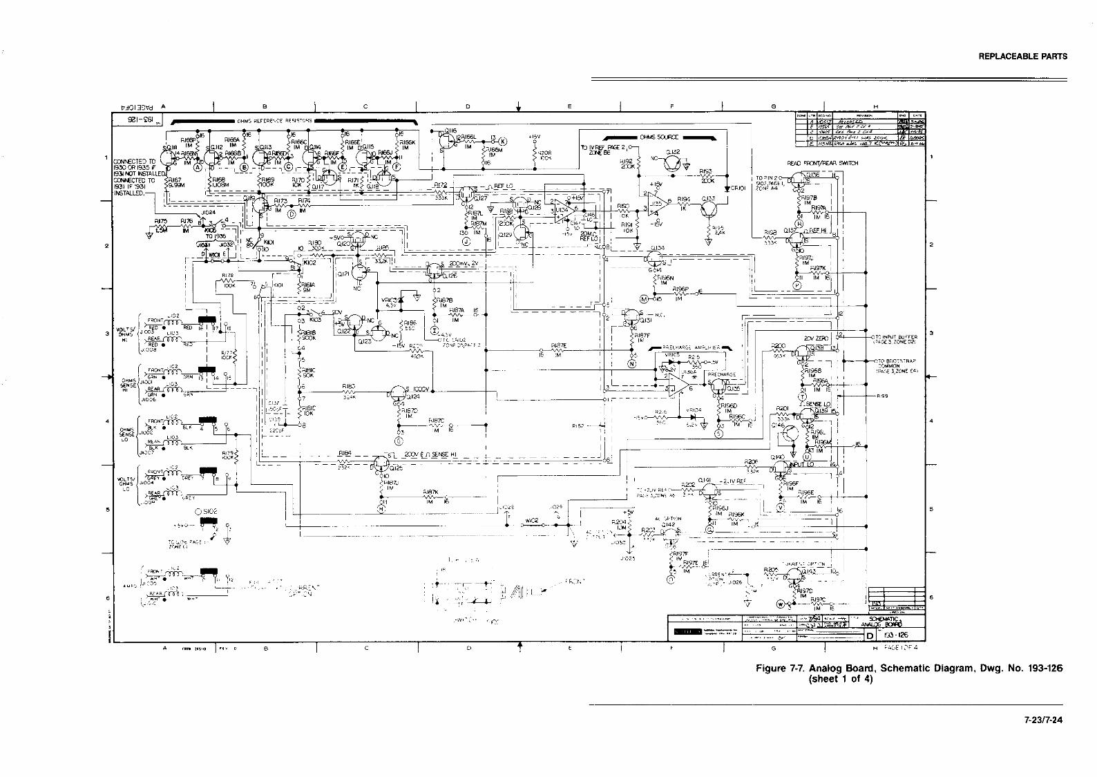
REPLACEABLE PARTS
c I " t t
Figure 7-7. Analog Board, Schematic Diagram, Dwg. No. 193-126 (sheet 1 of 4)
?-23/7-24

/-h..,..
E I F
-IL I
I u t
Figure 7-7. Analog Board, Schematic Diagram, Dwg. No. 193-126 (sheet 2 of 4)
7-2517-26

REPLACEABLE PARTS
Figure 7-7. Analog Board, Schematic Diagram, Dwg. No. 193-126 (sheet 3 of 4)
7-2717-28

t f 0

REPLACEABLEPARTS
Table 7-4. Model 1930. Parts List
Circuit Desig.
c401
%i c404 c405 C406 c407
%z c410 c411 c4l2 c413 c414
CR401 CR402 CR403
K401
I’1023 P1024 P1025
@
:% Q;g
8 408
R401 R402 R403
i%t R406 R407 R408 R409
E;: R4l2 R4l3 R414 R415 R416 R417 R4lB R419 R420
Description
Capacitor, Capacitor, Capacitor, Capacitor, Capacitor, Capacitor, Capacitor, Capacitor, Capacitor, Capacitor, Capacitor, Capacitor, Capacitor, Capacitor,
0.05& lOOa!!, Metal Polvstyrene
l.OpF, 5OV, Aluminum Electrol$ic 330
P; F, soov, Polystyrene
30~ , 5OOV. Mica
l.O@, 5Ov, Metalized P&carbonate 33uE 5OOV! Mica 6.g
’
$, 5OV,’ Tubular Ceramic 0.2 pF-1.5 F, 2oOOV Trimmer 0.75pF, 5 & Tub&r Ceramic
Diode, Silicon Diode, Silicon Dode, Silicon
Relay
Connector, Female, 12 pin Connector, Female, Lug Connector, Female, Lug
2N4392 2N4392 2N4392 Selected 2N4392 Selected
2N4392
2N4392
Resistor, lk62, l%, ‘/qW, Metal Film Resistor, lk0, l%, ‘hW, Metal Film Resistor. 2M62. 0.5%. 1W. Metal Film Resistor, Pot, 1000, 10%; 3/4W Resistor, Pot, lkQ, lo%, YaW Resistor. Pot. 10kQ. 10%. 3hW Resistor, Resistor, Resistor, Resistor, Resistor, Resistor, Resistor, Resistor, Resistor, Resistor, Resistor, Resistor, Resistor, Resistor,
Pot, lko, lO%, %W 2.l2k61, 0.5%, ZW, Metal Film 19.6kR, 0.5%, SW, Metal Film 217k0, 0.5%, XW, Metal Film Pot, lOOka, lo%, %W lMQ, lo%, s/aW, Composition lOkl?, 5%, ‘hW, Composition lOk0, 5%, ‘/aW, Composition lMlI, lo%, XW, Composition lOkbl, 5%, XW, Composition lM0, lo%, XW, Composition 2Mfl, 0.5%, ZW, Metal Film 3.65k0, l%, ZW, Composition 24kn, 5%, XW, Composition
Schematic Location I Keithley
Part No.
C-285-.05 C-343 C-325-1.0 c-325-1.0 c-l3&33op w;;-3op
C-335-1.2 c-335-1.0 c-335-1.0 C-236.33~ ~~&1&6.“p
C-282..75p
RF28 RF28 RF28
RL-69
CS-337.12 LU-90 LU-90
TG-84 TG-128 TG -77 TG-128 l-G-77 TG-128 TG-77 ‘TG-118
R-3U7-lk R-3~.lk R-303.2M
gg:go RP-89.10k RP-89.lk R-246-2.12k I<-246.19.6k R-246.217k RP-89.100k R-76.1M R-76.10k R-76.10k R-76-1M R-76.10k R-76.1M R-246-2.0M R-88.3.65k R-76.24k
7-31

REPLACEABLE PARTS
Table 7-4. Model 1930, Parts List (Cont.)
Circuit Schematic Keithley Desig. Description Location Part No.
R421
E% R424 R425 R42b R427
EG R430 R431 R432 R433
E% R43b
u401 U402 u403
Resistor, lOOk& l%, m, Composition Resistor, 22SX 5%, SW, Composition Resistor, 2.2kR, 5%, ‘SW, Composition Resistor, 3.3k63, 5%, ‘XW, Composition Resistor, 2.2k0, 5%, ‘LW, Composition Resistor, Pot, lllOk0, lo%, %W Resistor, 2.2kR,5%, XW, Composition Resistor 499n 1% ZW Corn osition Resistor 56.2lh 0:5%, ‘$W getal Film Resistor: 56,2kd 0.5%, %Wl Metal Film Resistor, 44.2k0, l%, XW, Composition Resistor, lOOk0, 5%, ‘/aW, Composition Resistor, 169t?, l%, LW, Composition Resistor, 33kfl, 5%, ‘/aW, Composition Resistor, 100, 5%, XW, Composition Resistor, 104 5%, ‘SW, Composition
Monolithic JFET Input Op Am Volta
8 e Quad Comparator, LM I; 39
TRM -to-DC Converter
R-88-100k R-76-22 R-7b-2.2k R-7b-3.3k R-7b-2.2k RF-ill-100k R-7b-2.2k R-88-499 R-246-56.2k R-246-56.2k R-88.44.2k R-76.1OOk R-88-169 R-76.33k R-76-10 R-7b-10
IC-I52 IC-219 IC-305
7-32


REPLACEABLE PARTS
Figure 7-8. Model 1930, Component Location Drawing, Dwg. No. 1930-100
7-34

REPLACEABLEPARTS
Figure 7-9. Model 1930, Schematic Diagram, Dwg. No. 1930-106
7-3517-36


REPLACEABLEPARTS
Circuit Desig.
Cl01 Cl02 Cl03 Cl04
CR101 CR102 CR103
J1024
KlOl K102
E: K105 KlOb K107
E2 I’1027 I’1028 I’1029
RlOl R102 R103 R104 R105 RlOb
%i
UlOl u102 u103
Table 7-5. Model 1931, Parts List
Description
Capacitor, lOpF, 25V, Aluminum Electrolytic Capacitor, lo& 25V, Aluminum Electrolytic Capacitor, lo@, 25V, Aluminum Electrolytic Capacitor, O.l@, 5OV, Ceramic Film
Rectifier, PE05 Recitifer, Silicon, MR501 Rectifier, Silicon, PF40
Contact Pin
::kg z:: Relay, 5V Relay, 5V Relay, 5V
Connector, Female, lug Connector, Female, 12 pin Connector, Female, lug Connector, Female, lug Connector, Female, lug
Resistor, 0.10, O.l%, ZSW, Wirewound Resistor, 0.8984 O.l%, 5W, Wirewound Resistor, 9fl Resistor, 904 O.l%, %W, Metal Film Resistor, 9004 O.l%, X,W, Metal Film Resistor, l.O05kQ, O.l%, &W, Metal Film Resistor, 8.95k63, O.l%, XOW, Metal Film Resistor, lOk0, lo%, 2W, Composition
Darlington Transistor Array, ULN2003A 0 erational Amp., JFET 8 I- tage Shift/Store Register, MC14094BCP
Schematic Location
E2
Ei B2
85
E
El
El A2 85 86 Ab
SW E2 83
Keithley - Part No.
c-314-10 c-31410 c-314-10 C-237-.1
RF-48 RF34 RF46
CS-357
RI:73 RL-73
;k::; RL-49 RL-69 RL-69
LE.90 CS-337.12 LU-90 LU-90 LE.90
R-262-0.1 R-310-.898 R-252-9 lb169.9C R-168-900 I<-263.1.005k R-263.8.95k R-3.10k
IC-206 IC-342 IC-251
7-37

REPLACEABLE PARTS
ij k 5
I
-I -
1
Figure 7-10. Model 1931, Component Location Drawing, Dwg. No. 1931-100
7-38
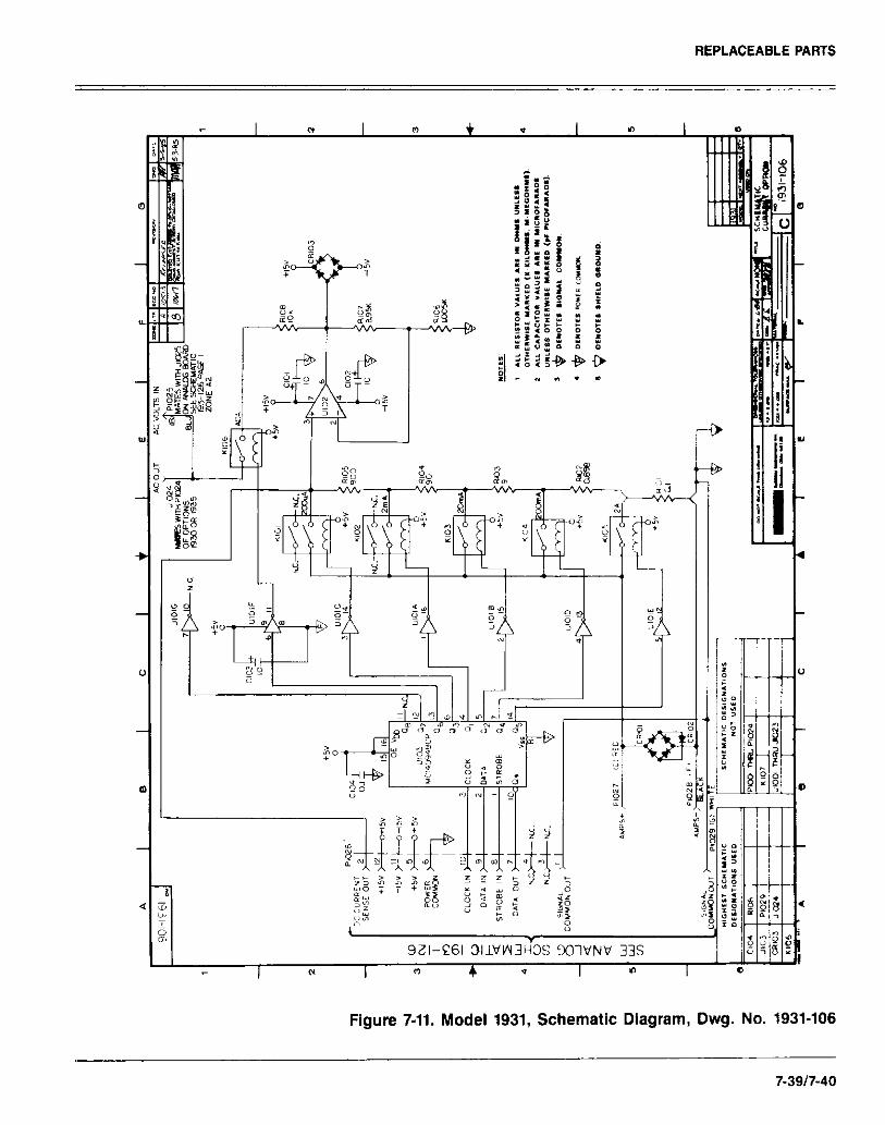
REPLACEABLE PAWS
Figure 7-11. Model 1931, Schematic Diagram, Dwg. No. 1931-106


REPLACEABLE PARTS
Table 7-6. Model 193A Mechanical Parts List
Quantity Description Keithky Part No.
; Side Panel Assembl Front Bezel Assemb y 7
: Front Panel
:
prl;oyel Overlay 193A-303 193.327
Banana Jacks (Black) BJ-12-O 4 Banana Jacks (Red) 81-12-2
i %%%% &%%t Lights) BJ-X2-9 MK-22-l
3 Pushbuttons (Range) 228-317-4
2 Pushbuttons (Function) 228-317-5 Pushbuttons (Modifier) 228-317-6
7 Pushbuttons (Control and Local) I 228-317-7
: Pushbutton Power) i 29465-3
/ 29465-2 4 228.318 1
&$%?(&%$lay Board) Rear Panel Assem ly i 19W305
i BNC Connectors (IS-249 Mountin Rails 228.319
?i Fuse Ho ders F FH-21 Fuse Carriers FH-25
1 Fuse Carrier (Euro can, Current) FH-26
: Heat Sink (for V Rf 01) HS-21 Heat Sink HS-22 Shield (Mother Board) 193.312
FA-167.3 / FA-166-l
4 HP-22
i 193.316 FA-99
i 193.171 FA-167.5
5 FA-166-l
: Top Cover 228.312 Bottom Cover 228-313
; Feet (Rear) 706.316
706317
; #3=323 ¶93=3?3
1 co-7
Note: Some of these parts are shown in Figure 6-U.
7-4117-42


INDEX
Accessories, l-3 Addenda, 1-l Addressed Commands, 3-5, 3-7 Analog Circuitry, 5-l to 5-9
Baseline Levels, 2-9, Z-10 Bus Hold-off, 3-19, 3-32 Bus Line IEEE-488, 3-2
Calibration, 2-30, 3-19, 3-26, 6-3 DC Current, 6-13, 6-14 DC Volts, 6-7 6-8 Front Panel, 6-5 IEEE-488, 6-6 Resistance, 6-8, 6-9 TRMS AC Volts, 6.10, 6.11, 6-12
Caution, l-l Command Codes, 3-5, 3-6 Component Location Drawings, 7-1 Cant&s, Table of, i - Control Circuitry, 5-10
Default Conditions (L), Z-1, 3-15, 3-19, 3-27
Delay (W), 3-20, 3-37 Device Clear Command (DCL), 3-4,
3.14. 3-15 De&De endent Command List, 3-18, 3-19, E; 20
Diagnostic Program, 6-23 Digital Circuitry, 5-10 Disassembly Instructions, 6-15, 6-16 Display, (D), 3-20, 3-39
End Or Identify (EOI), 3-2, 3-4, 3-19, 3-31
Error Messages, 2-6, Z-7 3-41, 3-42 Execute (X), 3.18, 3-20
Factory Default Conditions, 2-1, 3-15 Filter, 2.11, Z-22, 2-26, 3-18, 3-22 Front Panel
Detailed Description, 2-2, 2-4 Calibration. 6-5
Data Format (G), 3-19, 3-27, 3-28 Data Store, 2-22, 2-23
Rate (Q), 3-19, 3-24, 3-25 Size (I), 3-19, 3-24
Data Transmission Times, 3-40, 3-41 Go To Local (GTL), 3-14
Figure, 2-7 Function (F), 3.18, 3-20 Fuses, 6-l
Group Execute Trigger (GET), 3-15, 3-16
Handshake Sequence, 3-3 Hardware Considerations, 3-7, 3-8, 3-9 Hit Button, 3-20, 3-38, 3-39
IEEE-488 Interface Bus Calibration, 6-6 Device-Dependent Commands, 3-5, 3-7, 3-17
General Description, 3-1 Hardware Considerations, 3-7, 3-8, 3-9
Software Considerations, 3-K SRQ 3-19, 3-28, 3.29, 3-30 Status, 3-19, J-33, 3-34, 3-35
Illustrations, v Installation, 1930, 6-2, 6-4 Installation, 1931, 6-3, 6-4 Interface Clear (IFC), 3-4, 3-13, 3-14 Interface Function Codes, 3-11, 3-12
Line Voltage Selection, 6-l Local Lockout (LLO). 3-4, 3-14
Maintenance, 6-I

Measurement Techniques Current, 2-15, 2-16 dB, 2.17, 2-18 DC Voltage, 2-12, 2-13 Resistance, 2-14, 2-15 RTD Tern 2-16
c? TRMS A +DC, 2-19, 2-20, 2.21 TRMS AC Voltage, 2.13, 2.14
Multiplex (A), 3-20, 3-36, 3-37
Operation, General, 1-2, l-3
Performance Verification, 4-l Power Supplies, 5-10 Power up, 2-l Primary Address, 3-10 Programs
AC + DC, 2-25, 2-26 Cursor, Data Entry, 2-25 dB, 2-26 Filter, 2-26 PI-e. 4. 2-27 rrp 90, 2-28 l’rg 91, 2-28 Pre 92, 2-29 Pri 93; 2-29, 6-23 Prg 94, 2-29 Prg 95, 2-30 Prg 96, 2-30 Reset. 2-27 Tap; 2-25 Zero, 2-26
Programmed Conditions, 2-2
Rack Mount Kits, l-4
Range (R), 3-18, 3-21 Reading Mode (B), 3-18, 3-24 Reading Rate (S), 3-18, 3-22 Rear Panel
Detailed Description, 2-4 Figure, 2-7
Recommended Calibration Equipment, 6-3, 6-5
Recommended Test Equipment, 4-l Reference Junction (0), 3-20, 3.39 Remote Enable (REN), 3-2, 3-4, 3-13 “xk=&,e T
Mechani&l, 6-19, 7-41
Safety Precautions Preceding Set 1, 2-7
Safety Symbols and Terms, 1-l Schematic Diagrams, 8-l Selective Device Clear (SDC), 3.15 Self Test, 3-20, 3-37 Serial Poll (SPE) (SPD) 3-16 Service Information, see Maintenance Software Considerations, 3-10 Specifications
Preceding Table of Cont., 1-2 Static Sensitive Devices, 6-21 status
Format, 3-34 (U), 3-19, 3-33, 3-36 Word, 3-34, 3-35
Tables, List of, vii Terminator (Y), 3-19, 3-32 Theory of Operation, 5-l
Translator Combining Words, 3-44 FORGET, 3-45 Format, 3-42, 3-43 LIST. 3-45 NE+ and OLD, 3-43 Reserved Words, 3-42, 3-43, 3-44
Trigger External. 2-30. 2-31. 2-32 Mode (T), 3-18, 3-23 Voltmeter Complete, 2-31
Troubleshooting, 6-21 to 6-29
Uniline Commands, 3-4 Universal Commands, 3-4, 3-7
Value (V), 3-19, 3-26 Verification Procedure
DC Current. 4-4. 4-5 DC Volts, 4:2 Ohms, 4-3, 4-4 RTD Temp, 4-6, 4-7 TRMS AC Current, 4-5, 4-6 TRMS AC Volts, 4-2, 4-3
Warm Up, 2-7 Warnings, 1-l Warranty, 1-l
Zero, 2-24 Baseline Levels, 2-10 Corrections, 2-7, 2-8 Zero (Z), 3-18, 3-22
The number following each entry indicates the page number.

m lNSTRUMENTS SERVICE FORM
Model No. Name and Telephone No. Company
Serial No. Date
List all control settings, describe problem and check boxes that apply to problem.
q lIntermittent q Analog output follows display q jParticular range or function bad; specify q IIEEE failure q Obvious problem on power-up q Batteries and fuses are OK aFront panel operational OAll ranges or functions are bad q Checked all cables
Display or output (circle one)
norifts nUnable to zero q Unstable q Will not read applied input q Overload
[7Calibration only q Data required
UC of C required
(attach any additional sheets as necessary.)
Show a block diagram of your measurement system including all instruments connected (whether power IS tumcd on or no! 1 Also, describe signal source.
Where is the measurement being performed? (factory, controlled laboratory, out-of-doors. etc.)
What power line voltage is used? Ambient Temperature?
Relative humidity? Other?
Any additional information. (If special modifications have been made by the user, please describe.)