Embed Size (px)
Citation preview
SEDRA/SMITH
INSTRUCTOR’S SOLUTIONS MANUAL FOR
Microelectronic Circuits
INTERNATIONAL SEVENTH EDITION
Adel S. Sedra University of Waterloo
New York Oxford OXFORD UNIVERSITY PRESS

Oxford University Press is a department of the University of Oxford. It furthers the University’s objective of excellence in research, scholarship, and education by publishing worldwide. Oxford New York Auckland Cape Town Dar es Salaam Hong Kong Karachi Kuala Lumpur Madrid Melbourne Mexico City Nairobi New Delhi Shanghai Taipei Toronto
With offices in Argentina Austria Brazil Chile Czech Republic France Greece Guatemala Hungary Italy Japan Poland Portugal Singapore South Korea Switzerland Thailand Turkey Ukraine Vietnam Copyright 2017 by Oxford University Press Published by Oxford University Press 198 Madison Avenue, New York, New York 10016 http://www.oup.com Oxford is a registered trademark of Oxford University Press All rights reserved. No part of this publication may be reproduced, stored in a retrieval system, or transmitted, in any form or by any means, electronic, mechanical, photocopying, recording, or otherwise, without the prior permission of Oxford University Press. ISBN: 978-0-19-933916-7 Printing number: 9 8 7 6 5 4 3 2 1 Printed in the United States of America on acid-free paper
For titles covered by Section 112 of the US Higher Education Opportunity Act, please visit www.oup.com/us/he for the latest information about pricing and alternate formats.
Contents Exercise Solutions (Chapters 1-17) Problem Solutions (Chapters 1-17)

Preface
This Instructor’s Solution Manual (ISM) contains complete solutions for all exercises and end-of-chapter problems included in the book Microelectronic Circuits, International Seventh Edition by Adel S. Sedra and Kenneth C. Smith.
Most of the solutions are new; however, I have used and/or adapted some of the solutions from the ISM of the International Sixth Edition. Credit for these goes to the problem solvers listed therein.
This manual has greatly benefited from the careful work of the accuracy checkers listed below. These colleagues and friends worked diligently to ensure that the 2,030 solutions are free of error. Despite all of our combined efforts, however, there is little doubt that some errors remain, and for these I take full responsibility. I will be most grateful to instructors who discover errors and point them out to me. Please send all corrections and comments by email to: [email protected].
Adel Sedra Waterloo, Ontario, Canada
October 2015
Accuracy Checkers • Professor Tony Chan Carusone, University of Toronto - Assisted by graduate students Jeffrey Wang and Luke Wang • Professor Vincent Gaudet, University of Waterloo • Professors Shahriar Mirabbasi and Mandana Amiri, University of British Columbia • ProfessorWai Tung Ng, University of Toronto • Professor Olivier Trescases, University of Toronto • Professor Amir Yazdani, Ryerson University
Exercise 1–1
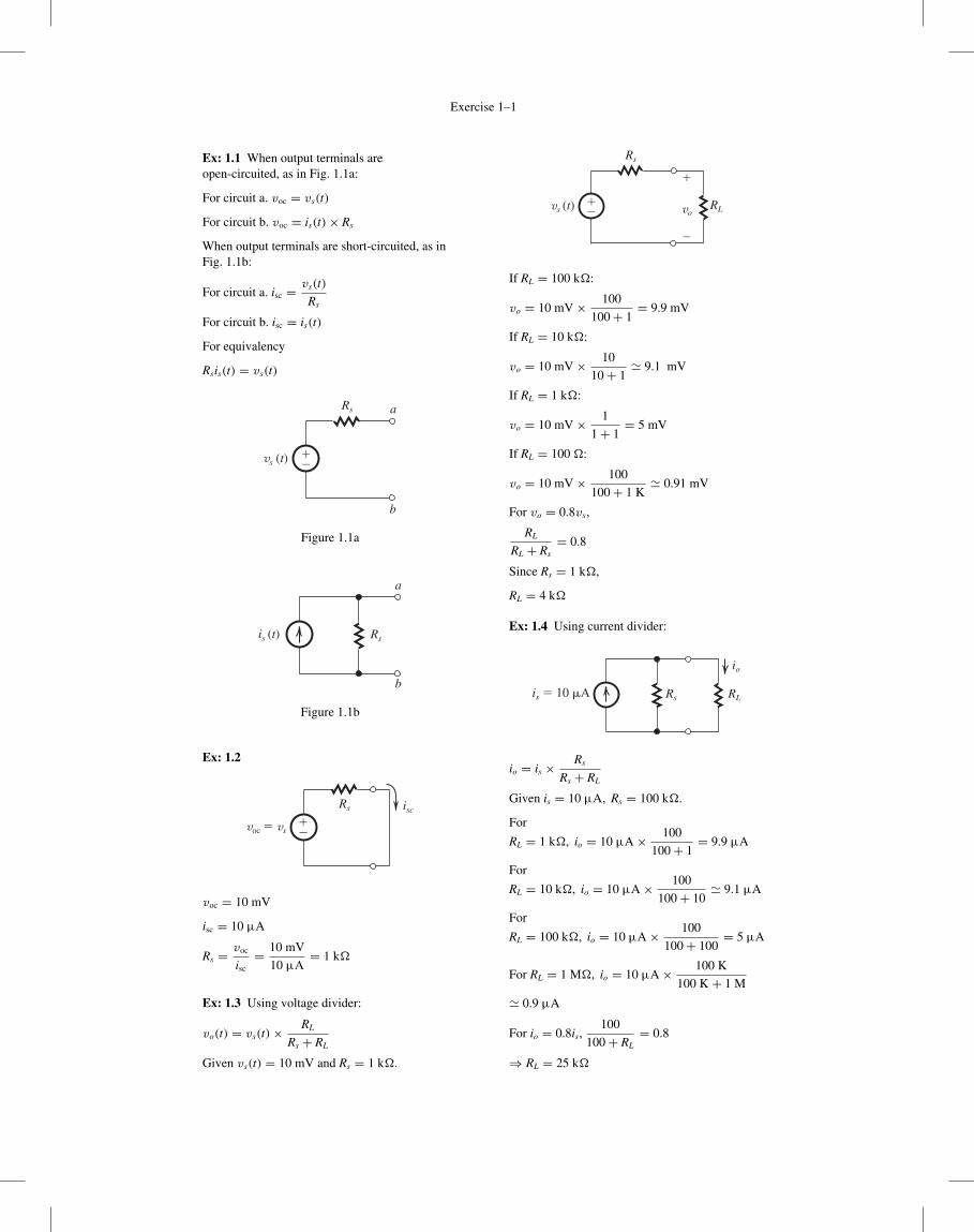
Ex: 1.1 When output terminals areopen-circuited, as in Fig. 1.1a:
For circuit a. voc = vs(t)
For circuit b. voc = is(t)× Rs
When output terminals are short-circuited, as inFig. 1.1b:
For circuit a. isc = vs(t)
Rs
For circuit b. isc = is(t)
For equivalency
Rsis(t) = vs(t)
Rs a
b
��
vs (t)
Figure 1.1a
is (t)
a
b
Rs
Figure 1.1b
Ex: 1.2
voc � vs
Rs
��
isc
voc = 10 mV
isc = 10 μA
Rs = voc
isc= 10 mV
10 μA= 1 k�
Ex: 1.3 Using voltage divider:
vo(t) = vs(t)× RL
Rs + RL
Given vs(t) = 10 mV and Rs = 1 k�.
vs (t) vo
Rs
��
�
�
RL
If RL = 100 k�:
vo = 10 mV × 100
100+ 1= 9.9 mV
If RL = 10 k�:
vo = 10 mV × 10
10+ 1� 9.1 mV
If RL = 1 k�:
vo = 10 mV × 1
1+ 1= 5 mV
If RL = 100 �:
vo = 10 mV × 100
100+ 1 K� 0.91 mV
For vo = 0.8vs,
RL
RL + Rs= 0.8
Since Rs = 1 k�,
RL = 4 k�
Ex: 1.4 Using current divider:
Rsis � 10 �A RL
io
io = is × Rs
Rs + RL
Given is = 10 μA, Rs = 100 k�.
For
RL = 1 k�, io = 10 μA × 100
100+ 1= 9.9 μA
For
RL = 10 k�, io = 10 μA × 100
100+ 10� 9.1 μA
For
RL = 100 k�, io = 10 μA × 100
100+ 100= 5 μA
For RL = 1 M�, io = 10 μA × 100 K
100 K + 1 M
� 0.9 μA
For io = 0.8is,100
100+ RL= 0.8
⇒ RL = 25 k�
Exercise 1–2
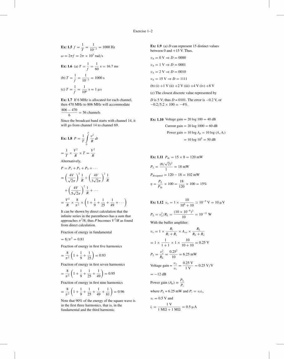
Ex: 1.5 f = 1
T= 1
10−3= 1000 Hz
ω = 2π f = 2π × 103 rad/s
Ex: 1.6 (a) T = 1
f= 1
60s = 16.7 ms
(b) T = 1
f= 1
10−3= 1000 s
(c) T = 1
f= 1
106s = 1 μs
Ex: 1.7 If 6 MHz is allocated for each channel,then 470 MHz to 806 MHz will accommodate
806− 470
6= 56 channels
Since the broadcast band starts with channel 14, itwill go from channel 14 to channel 69.
Ex: 1.8 P = 1
T
T∫0
v2
Rdt
= 1
T× V 2
R× T = V 2
R
Alternatively,
P = P1 + P3 + P5 + · · ·
=(
4V√2π
)2 1
R+(
4V
3√
2π
)2 1
R
+(
4V
5√
2π
)2 1
R+ · · ·
= V 2
R× 8
π2×(
1+ 1
9+ 1
25+ 1
49+ · · ·
)
It can be shown by direct calculation that theinfinite series in the parentheses has a sum thatapproaches π2/8; thus P becomes V 2/R as foundfrom direct calculation.
Fraction of energy in fundamental
= 8/π2 = 0.81
Fraction of energy in first five harmonics
= 8
π2
(1+ 1
9+ 1
25
)= 0.93
Fraction of energy in first seven harmonics
= 8
π2
(1+ 1
9+ 1
25+ 1
49
)= 0.95
Fraction of energy in first nine harmonics
= 8
π2
(1+ 1
9+ 1
25+ 1
49+ 1
81
)= 0.96
Note that 90% of the energy of the square wave isin the first three harmonics, that is, in thefundamental and the third harmonic.
Ex: 1.9 (a) D can represent 15 distinct valuesbetween 0 and +15 V. Thus,
vA = 0 V⇒ D = 0000
vA = 1 V⇒ D = 0001
vA = 2 V⇒ D = 0010
vA = 15 V⇒ D = 1111
(b) (i) +1 V (ii) +2 V (iii) +4 V (iv) +8 V
(c) The closest discrete value represented by
D is 5 V; thus D = 0101. The error is −0.2 V, or−0.2/5.2× 100 = −4%.
Ex: 1.10 Voltage gain = 20 log 100 = 40 dB
Current gain = 20 log 1000 = 60 dB
Power gain = 10 log Ap = 10 log (Av Ai)
= 10 log 105 = 50 dB
Ex: 1.11 Pdc = 15× 8 = 120 mW
PL = (6/√
2)2
1= 18 mW
Pdissipated = 120− 18 = 102 mW
η = PL
Pdc× 100 = 18
120× 100 = 15%
Ex: 1.12 vo = 1× 10
106 + 10� 10−5 V = 10 μV
PL = v2o/RL = (10× 10−6)2
10= 10−11 W
With the buffer amplifier:
vo = 1× Ri
Ri + Rs× Avo × RL
RL + Ro
= 1× 1
1+ 1× 1× 10
10+ 10= 0.25 V
PL = v2o
RL= 0.252
10= 6.25 mW
Voltage gain =vo
vs= 0.25 V
1 V= 0.25 V/V
= −12 dB
Power gain (Ap) ≡ PL
Pi
where PL = 6.25 mW and Pi = v i i1,
v i = 0.5 V and
ii = 1 V
1 M�+ 1 M�= 0.5 μA
Exercise 1–3
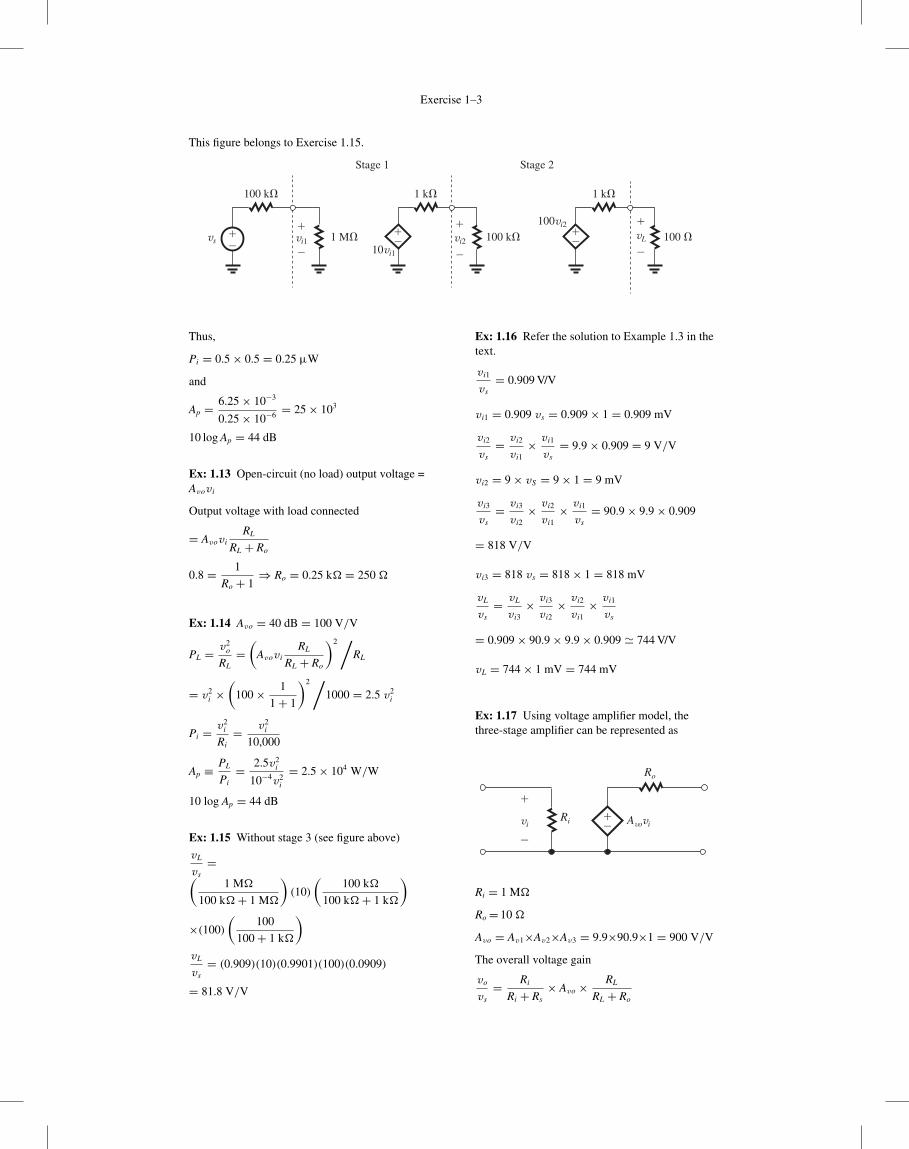
This figure belongs to Exercise 1.15.
��
��
�
�
�
�
�
�
vs vi110vi1
100 k�
1 M� vi2
1 k�
100 k�
100vi2
vL
1 k�
100 �
Stage 1 Stage 2
��
Thus,
Pi = 0.5× 0.5 = 0.25 μW
and
Ap = 6.25× 10⁻³
0.25× 10−6 = 25× 103
10 log Ap = 44 dB
Ex: 1.13 Open-circuit (no load) output voltage =Avov i
Output voltage with load connected
= Avov iRL
RL + Ro
0.8 = 1
Ro + 1⇒ Ro = 0.25 k� = 250 �
Ex: 1.14 Avo = 40 dB = 100 V/V
PL = v2o
RL=(
Avov iRL
RL + Ro
)2 /RL
= v2i ×
(100× 1
1+ 1
)2 /1000 = 2.5 v2
i
Pi = v2i
Ri= v2
i
10,000
Ap ≡ PL
Pi= 2.5v2
i
10−4v2i
= 2.5× 10⁴ W/W
10 log Ap = 44 dB
Ex: 1.15 Without stage 3 (see figure above)
vL
vs=(
1 M�
100 k�+ 1 M�
)(10)
(100 k�
100 k�+ 1 k�
)
×(100)
(100
100+ 1 k�
)vL
vs= (0.909)(10)(0.9901)(100)(0.0909)
= 81.8 V/V
Ex: 1.16 Refer the solution to Example 1.3 in thetext.
v i1
vs= 0.909 V/V
v i1 = 0.909 vs = 0.909× 1 = 0.909 mV
v i2
vs= v i2
v i1× v i1
vs= 9.9× 0.909 = 9 V/V
v i2 = 9× vS = 9× 1 = 9 mV
v i3
vs= v i3
v i2× v i2
v i1× v i1
vs= 90.9× 9.9× 0.909
= 818 V/V
v i3 = 818 vs = 818× 1 = 818 mV
vL
vs= vL
v i3× v i3
v i2× v i2
v i1× v i1
vs
= 0.909× 90.9× 9.9× 0.909 � 744 V/V
vL = 744× 1 mV = 744 mV
Ex: 1.17 Using voltage amplifier model, thethree-stage amplifier can be represented as
viRi
Ro
Avovi
�
�
��
Ri = 1 M�
Ro= 10 �
Avo = Av1×Av2×Av3 = 9.9×90.9×1 = 900 V/V
The overall voltage gain
vo
vs= Ri
Ri + Rs× Avo × RL
RL + Ro
Exercise 1–4
For RL = 10 �:
Overall voltage gain
= 1 M
1 M+ 100 K× 900× 10
10+ 10= 409 V/V
For RL = 1000 �:
Overall voltage gain
= 1 M
1 M+ 100 K× 900× 1000
1000+ 10= 810 V/V
∴ Range of voltage gain is from 409 V/V to810 V/V.
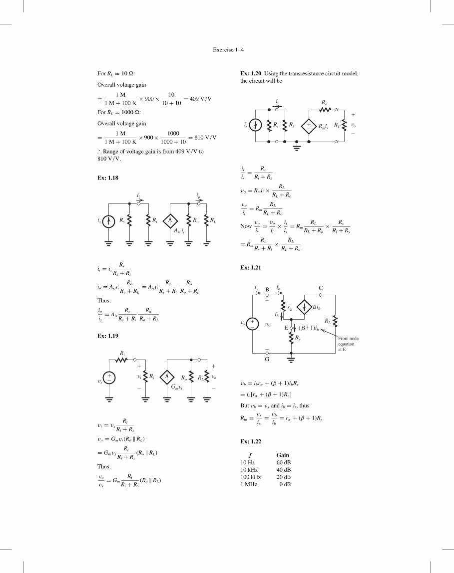
Ex: 1.18
ii io
Ais ii
RLRoRs Riis
ii = isRs
Rs + Ri
io = AisiiRo
Ro + RL= Aisis
Rs
Rs + Ri
Ro
Ro + RL
Thus,
io
is= Ais
Rs
Rs + Ri
Ro
Ro + RL
Ex: 1.19
Ri
Ro
Gmvi
RLRi�
�vi
�
�
�
�
vovs
v i = vsRi
Ri + Rs
vo = Gmv i(Ro ‖RL)
= GmvsRi
Ri + Rs(Ro ‖RL)
Thus,
vo
vs= Gm
Ri
Ri + Rs(Ro ‖RL)
Ex: 1.20 Using the transresistance circuit model,the circuit will be
RiRsis
ii Ro
RL voRmii�
�
��
ii
is= Rs
Ri + Rs
vo = Rmii × RL
RL + Ro
vo
ii= Rm
RL
RL + Ro
Nowvo
is= vo
ii× ii
is= Rm
RL
RL + Ro× Rs
Ri + Rs
= RmRs
Rs + Ri× RL
RL + Ro
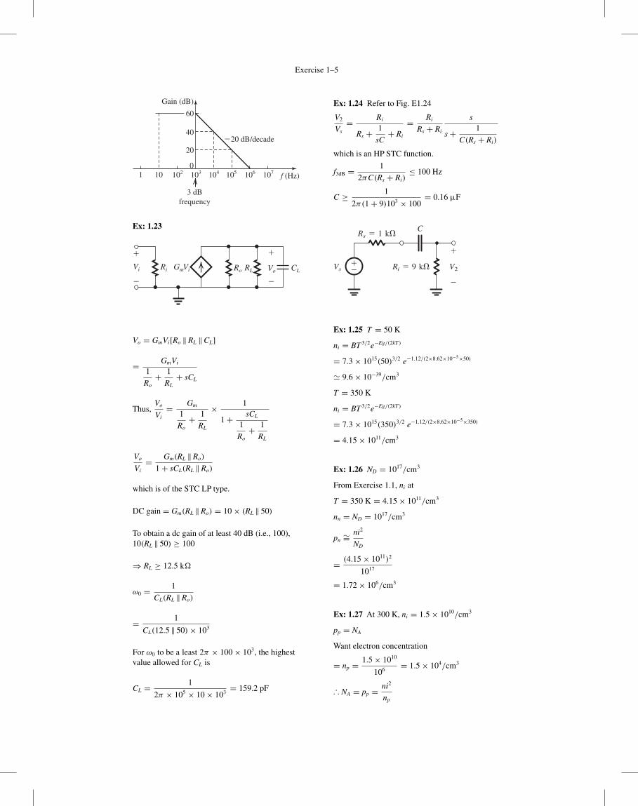
Ex: 1.21
vb = ibrπ + (β + 1)ibRe
= ib[rπ + (β + 1)Re]But vb = vx and ib = ix, thus
Rin ≡ vx
ix= vb
ib= rπ + (β + 1)Re
Ex: 1.22
f Gain10 Hz 60 dB10 kHz 40 dB100 kHz 20 dB1 MHz 0 dB
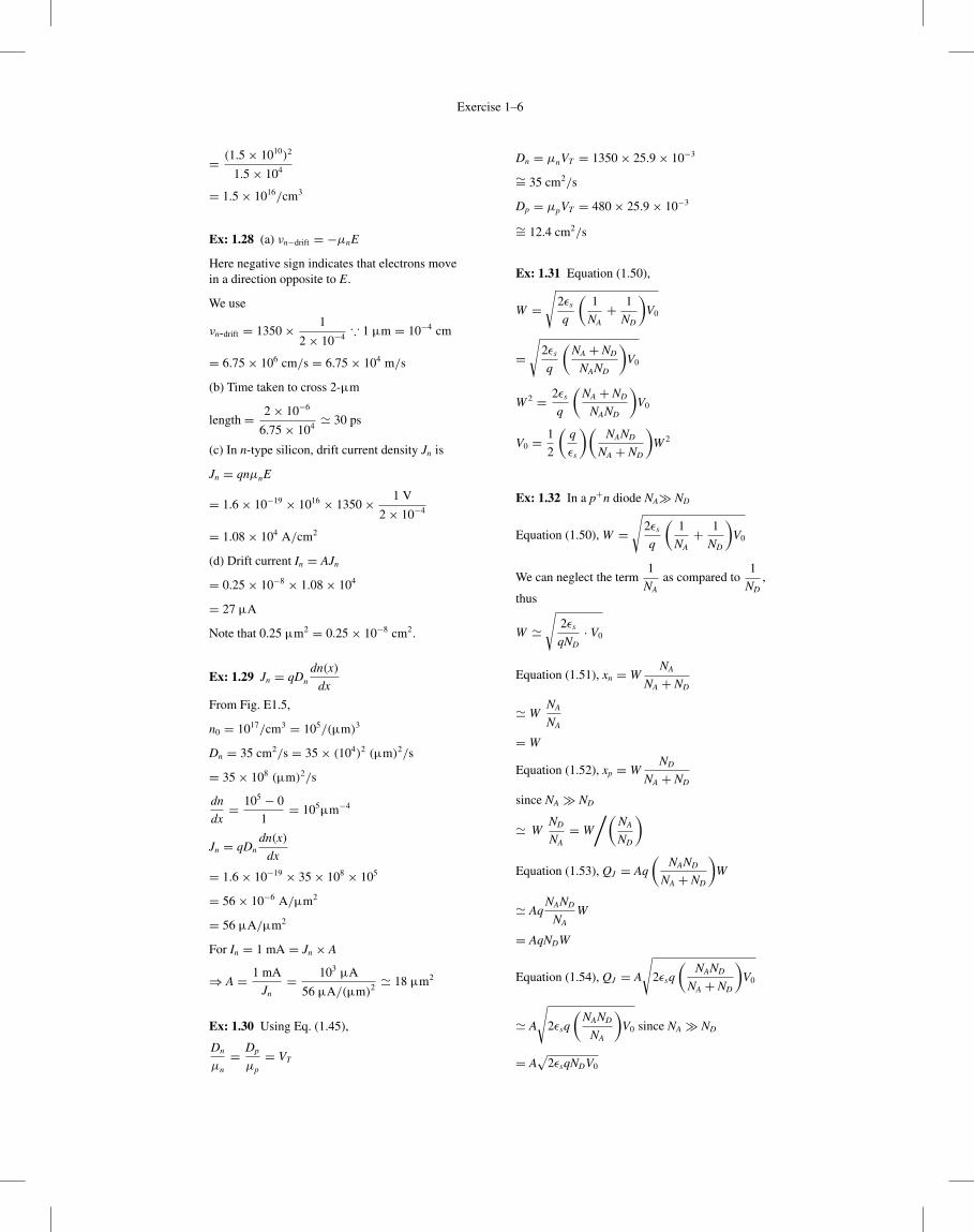
Exercise 1–5
Gain (dB)
�20 dB/decade
3 dBfrequency
0
20
40
60
1 10 10 10 10 10 10 10 f (Hz)
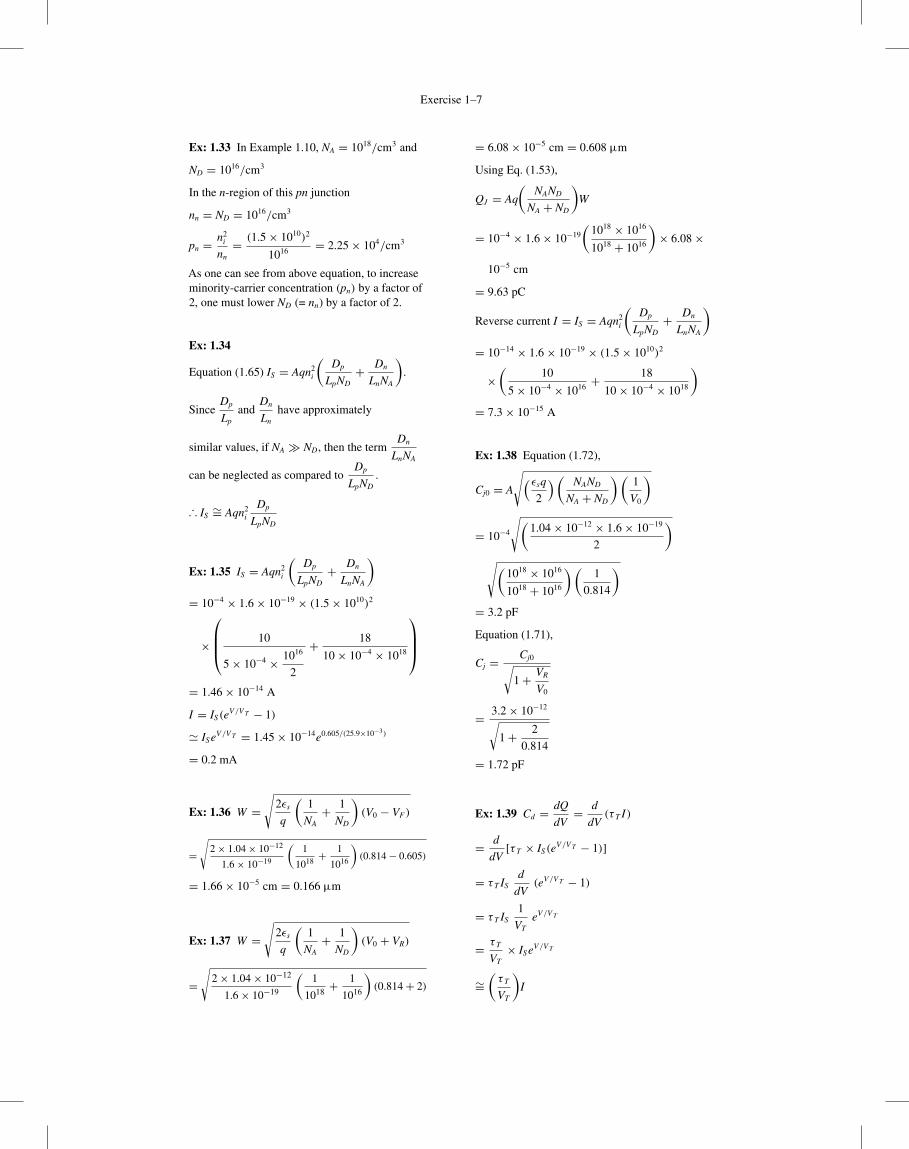
Ex: 1.23
RLRoRi ViVi Gm Vo CL
�
�
�
�
Vo = GmVi[Ro ‖RL ‖CL]
= GmVi
1
Ro+ 1
RL+ sCL
Thus,Vo
Vi= Gm
1
Ro+ 1
RL
× 1
1+ sCL
1
Ro+ 1
RL
Vo
Vi= Gm(RL ‖Ro)
1+ sCL(RL ‖Ro)
which is of the STC LP type.
DC gain = Gm(RL ‖Ro) = 10× (RL ‖ 50)
To obtain a dc gain of at least 40 dB (i.e., 100),10(RL ‖ 50) ≥ 100
⇒ RL ≥ 12.5 k�
ω0 = 1
CL(RL ‖Ro)
= 1
CL(12.5 ‖ 50)× 103
For ω0 to be a least 2π × 100× 103, the highestvalue allowed for CL is
CL = 1
2π × 105 × 10× 103 = 159.2 pF
Ex: 1.24 Refer to Fig. E1.24
V2
Vs= Ri
Rs + 1
sC+ Ri
= Ri
Rs + Ri
s
s+ 1
C(Rs + Ri)
which is an HP STC function.
f3dB = 1
2πC(Rs + Ri)≤ 100 Hz
C ≥ 1
2π(1+ 9)103 × 100= 0.16 μF
��Vs
C
V2
�
�
Rs � 1 k�
Ri � 9 k�
Ex: 1.25 T = 50 K
ni = BT 3/2e−Eg/(2kT )
= 7.3× 10¹⁵(50)3/2 e−1.12/(2×8.62×10−5×50)
� 9.6× 10−39/cm3
T = 350 K
ni = BT 3/2e−Eg/(2kT )
= 7.3× 10¹⁵(350)3/2 e−1.12/(2×8.62×10−5×350)
= 4.15× 10¹¹/cm3
Ex: 1.26 ND = 1017/cm3
From Exercise 1.1, ni at
T = 350 K = 4.15× 10¹¹/cm3
nn = ND = 1017/cm3
pn∼= ni2
ND
= (4.15× 10¹¹)2
1017
= 1.72× 10⁶/cm3
Ex: 1.27 At 300 K, ni = 1.5× 10¹⁰/cm3
pp = NA
Want electron concentration
= np = 1.5× 10¹⁰
106 = 1.5× 10⁴/cm3
∴ NA = pp = ni2
np
Exercise 1–6
= (1.5× 10¹⁰)2
1.5× 104
= 1.5× 10¹⁶/cm3
Ex: 1.28 (a) νn−drift = −μnE
Here negative sign indicates that electrons movein a direction opposite to E.
We use
νn-drift = 1350× 1
2× 10⁻⁴ ∵ 1 μm = 10−4 cm
= 6.75× 106 cm/s = 6.75× 10⁴ m/s
(b) Time taken to cross 2-μm
length = 2× 10⁻⁶
6.75× 10⁴ � 30 ps
(c) In n-type silicon, drift current density Jn is
Jn = qnμnE
= 1.6× 10−19 × 1016 × 1350× 1 V
2× 10−4
= 1.08× 10⁴ A/cm2
(d) Drift current In = AJn
= 0.25× 10−8 × 1.08× 104
= 27 μA
Note that 0.25 μm2 = 0.25× 10⁻⁸ cm2.
Ex: 1.29 Jn = qDn
dn(x)
dx
From Fig. E1.5,
n0 = 1017/cm3 = 105/(μm)3
Dn = 35 cm2/s = 35× (104)2 (μm)2/s
= 35× 108 (μm)2/s
dn
dx= 105 − 0
1= 105μm−4
Jn = qDndn(x)
dx
= 1.6× 10−19 × 35× 108 × 105
= 56× 10−6 A/μm2
= 56 μA/μm2
For In = 1 mA = Jn × A
⇒ A = 1 mA
Jn= 103 μA
56 μA/(μm)2 � 18 μm2
Ex: 1.30 Using Eq. (1.45),
Dn
μn
= Dp
μp
= VT
Dn = μnVT = 1350× 25.9× 10−3
∼= 35 cm2/s
Dp = μpVT = 480× 25.9× 10−3
∼= 12.4 cm2/s
Ex: 1.31 Equation (1.50),
W =√
2εs
q
(1
NA+ 1
ND
)V0
=√
2εs
q
(NA + ND
NAND
)V0
W 2 = 2εs
q
(NA + ND
NAND
)V0
V0 = 1
2
(q
εs
)(NAND
NA + ND
)W 2
Ex: 1.32 In a p+n diode NA ND
Equation (1.50), W =√
2εs
q
(1
NA+ 1
ND
)V0
We can neglect the term1
NAas compared to
1
ND,
thus
W �√
2εs
qND· V0
Equation (1.51), xn = WNA
NA + ND
� WNA
NA
= W
Equation (1.52), xp = WND
NA + ND
since NA ND
� WND
NA= W
/(NA
ND
)
Equation (1.53), QJ = Aq
(NAND
NA + ND
)W
� AqNAND
NAW
= AqNDW
Equation (1.54), QJ = A
√2εsq
(NAND
NA + ND
)V0
� A
√2εsq
(NAND
NA
)V0 since NA ND
= A√
2εsqNDV0
Exercise 1–7
Ex: 1.33 In Example 1.10, NA = 1018/cm3 and
ND = 1016/cm3
In the n-region of this pn junction
nn = ND = 1016/cm3
pn = n2i
nn= (1.5× 10¹⁰)2
1016 = 2.25× 10⁴/cm3
As one can see from above equation, to increaseminority-carrier concentration (pn) by a factor of2, one must lower ND (= nn) by a factor of 2.
Ex: 1.34
Equation (1.65) IS = Aqn2i
(Dp
LpND+ Dn
LnNA
).
SinceDp
Lpand
Dn
Lnhave approximately
similar values, if NA ND, then the termDn
LnNA
can be neglected as compared toDp
LpND.
∴ IS∼= Aqn2
i
Dp
LpND
Ex: 1.35 IS = Aqn2i
(Dp
LpND+ Dn
LnNA
)
= 10−4 × 1.6× 10−19 × (1.5× 1010)2
×
⎛⎜⎜⎝ 10
5× 10−4 × 1016
2
+ 18
10× 10−4 × 1018
⎞⎟⎟⎠
= 1.46× 10⁻¹⁴ A
I = IS(eV /V T − 1)
� ISeV /V T = 1.45× 10⁻¹⁴e0.605/(25.9×10−3)
= 0.2 mA
Ex: 1.36 W =√
2εs
q
(1
NA+ 1
ND
)(V0 − VF )
=√
2× 1.04× 10−12
1.6× 10⁻¹⁹
(1
1018+ 1
1016
)(0.814− 0.605)
= 1.66× 10⁻⁵ cm = 0.166 μm
Ex: 1.37 W =√
2εs
q
(1
NA+ 1
ND
)(V0 + VR)
=√
2× 1.04× 10−12
1.6× 10⁻¹⁹
(1
1018+ 1
1016
)(0.814+ 2)
= 6.08× 10⁻⁵ cm = 0.608 μm
Using Eq. (1.53),
QJ = Aq
(NAND
NA + ND
)W
= 10−4 × 1.6× 10−19
(1018 × 1016
1018 + 1016
)× 6.08×
10−5 cm
= 9.63 pC
Reverse current I = IS = Aqn2i
(Dp
LpND+ Dn
LnNA
)
= 10−14 × 1.6× 10−19 × (1.5× 1010)2
×(
10
5× 10−4 × 1016 +18
10× 10−4 × 1018
)
= 7.3× 10⁻¹⁵ A
Ex: 1.38 Equation (1.72),
Cj0 = A
√( εsq
2
)( NAND
NA + ND
)(1
V0
)
= 10−4
√(1.04× 10−12 × 1.6× 10−19
2
)√(
1018 × 1016
1018 + 1016
)(1
0.814
)
= 3.2 pF
Equation (1.71),
Cj = Cj0√1+ VR
V0
= 3.2× 10⁻¹²√1+ 2
0.814
= 1.72 pF
Ex: 1.39 Cd = dQ
dV= d
dV(τ T I)
= d
dV[τ T × IS(e
V /V T − 1)]
= τ T ISd
dV(eV /V T − 1)
= τ T IS1
VTeV /V T
= τ T
VT× ISeV /V T
∼=(
τ T
VT
)I
Exercise 1–8
Ex: 1.40 Equation (1.75),
τ p =L2
p
Dp
= (5× 10⁻⁴)2
10
= 25 ns
Equation (1.81),
Cd =(
τ T
VT
)I
In Example 1.10, NA = 1018/cm3,
ND = 1016/cm3
Assuming NA ND,
τ T � τ p = 25 ns
∴ Cd =(
25× 10−9
25.9× 10⁻³
)0.1× 10−3
= 96.5 pF
Chapter 1–1
1.1 (a) I = V
R= 5 V
1 k�= 5 mA
(b) R = V
I= 5 V
1 mA= 5 k�
(c) V = IR = 0.1 mA × 10 k� = 1 V
(d) I = V
R= 1 V
100 �= 0.01 A = 10 mA
Note: Volts, milliamps, and kilohms constitute aconsistent set of units.
1.2 (a) P = I 2R = (20× 10−3)2 × 1× 103
= 0.4 W
Thus, R should have a1
2-W rating.
(b) P = I 2R = (40× 10−3)2 × 1× 103
= 1.6 W
Thus, the resistor should have a 2-W rating.
(c) P = I 2R = (1× 10⁻³)2 × 100× 103
= 0.1 W
Thus, the resistor should have a1
8-W rating.
(d) P = I 2R = (4× 10⁻³)2 × 10× 103
= 0.16 W
Thus, the resistor should have a1
4-W rating.
(e) P = V 2/R = 202/(1× 103) = 0.4 W
Thus, the resistor should have a1
2-W rating.
(f) P = V 2/R = 112/(1× 103) = 0.121 W
Thus, a rating of1
8W should theoretically suffice,
though1
4W would be prudent to allow for
inevitable tolerances and measurement errors.
1.3 (a) V = IR = 5 mA × 1 k� = 5 V
P = I 2R = (5 mA)2 × 1 k� = 25 mW
(b) R = V /I = 5 V/1 mA = 5 k�
P = VI = 5 V × 1 mA = 5 mW
(c) I = P/V = 100 mW/10 V = 10 mA
R = V /I = 10 V/10 mA = 1 k�
(d) V = P/I = 1 mW/0.1 mA
= 10 V
R = V /I = 10 V/0.1 mA = 100 k�
(e) P = I 2R⇒ I = √P/R
I = √1000 mW/1 k� = 31.6 mA
V = IR = 31.6 mA × 1 k� = 31.6 V
Note: V, mA, k�, and mW constitute a consistentset of units.
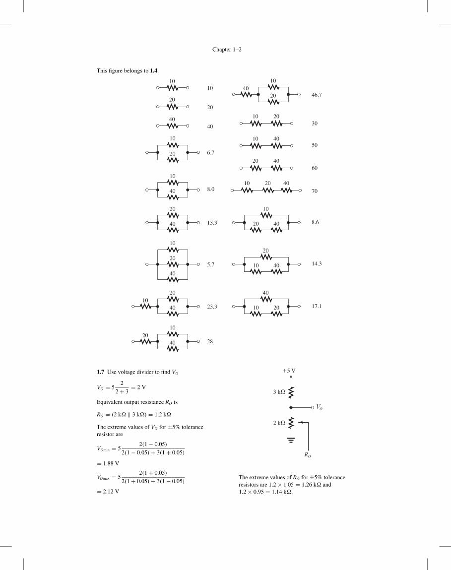
1.4 See figure on next page, which shows thatthere are 17 possible resistance values: 5.7, 6.7, 8,8.6, 10, 13.3, 14.3, 17.1, 20, 23.3, 28, 30, 40,46.7, 50, 60, and 70 k�.
1.5 Shunting the 10 k� by a resistor of value of Rresult in the combination having a resistance Req,
Req = 10R
R+ 10
Thus, for a 1% reduction,
R
R+ 10= 0.99⇒ R = 990 k�
For a 5% reduction,
R
R+ 10= 0.95⇒ R = 190 k�
For a 10% reduction,
R
R+ 10= 0.90⇒ R = 90 k�
For a 50% reduction,
R
R+ 10= 0.50⇒ R = 10 k�
Shunting the 10 k� by
(a) 1 M� results in
Req = 10× 1000
1000+ 10= 10
1.01= 9.9 k�
a 1% reduction;
(b) 100 k� results in
Req = 10× 100
100+ 10= 10
1.1= 9.09 k�
a 9.1% reduction;
(c) 10 k� results in
Req = 10
10+ 10= 5 k�
a 50% reduction.
1.6 VO = VDDR2
R1 + R2
To find RO , we short-circuit VDD and look backinto node X,
RO = R2 ‖ R1 = R1R2
R1 + R2
Chapter 1–2
This figure belongs to 1.4.
10
20
40
10
20
10
40
20
40
20
4010
10
4020
10
2040
10
20
40
10
20 40
20
10 40
40
10 20
28
23.3
5.7
13.3
8.0
6.7
40
20
1046.7
30
50
60
70
20 40
10 40
10 20
10 20 40
8.6
14.3
17.1
1.7 Use voltage divider to find VO
VO = 52
2+ 3= 2 V
Equivalent output resistance RO is
RO = (2 k� ‖ 3 k�) = 1.2 k�
The extreme values of VO for ±5% toleranceresistor are
VOmin = 52(1− 0.05)
2(1− 0.05)+ 3(1+ 0.05)
= 1.88 V
VOmax = 52(1+ 0.05)
2(1+ 0.05)+ 3(1− 0.05)
= 2.12 V
�5 V
VO
RO
3 k�
2 k�
The extreme values of RO for ±5% toleranceresistors are 1.2× 1.05 = 1.26 k� and1.2× 0.95 = 1.14 k�.
Chapter 1–3
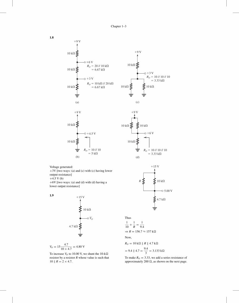
1.8
10 k�
10 k� 10 k�
�9 V
�6 V
�3 V
�6 V
10 k�
(a)
(d)
10 k�
10 k�
�3 V
�9 V
10 k�
(c)
10 k� 10 k�
�9 V
�4.5 V
(b)
10 k�
10 k�
R � 10 // 10 // 10 � 3.33 k�
R � 10 // 10 // 10 � 3.33 k�
R � 10 k� // 20 k� � 6.67 k�
R � 20 // 10 k� � 6.67 k�
R � 10 // 10 � 5 k�
�9 V
Voltage generated:+3V [two ways: (a) and (c) with (c) having loweroutput resistance]+4.5 V (b)+6V [two ways: (a) and (d) with (d) having alower output resistance]
1.9
10 k�
4.7 k�
�15 V
VO
VO = 154.7
10+ 4.7= 4.80 V
To increase VO to 10.00 V, we shunt the 10-k�
resistor by a resistor R whose value is such that10 ‖ R = 2× 4.7.
�15 V
5.00 V
10 k�
4.7 k�
R
Thus
1
10+ 1
R= 1
9.4
⇒ R = 156.7 ≈ 157 k�
Now,
RO = 10 k� ‖ R ‖ 4.7 k�
= 9.4 ‖ 4.7 = 9.4
3= 3.133 k�
To make RO = 3.33, we add a series resistance ofapproximately 200 �, as shown on the next page.
Chapter 1–4
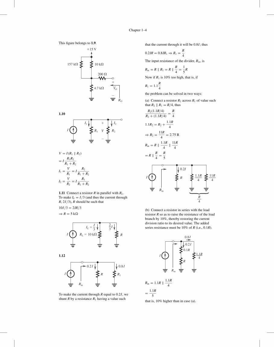
This figure belongs to 1.9.
�15 V
10 k�157 k�
200 �
�
�
RO
VO4.7 k�
1.10
I2I1
I V
�
�
R2R1
V = I(R1 ‖ R2)
= IR1R2
R1 + R2
I1 = V
R1= I
R2
R1 + R2
I2 = V
R2= I
R1
R1 + R2
1.11 Connect a resistor R in parallel with RL.To make IL = I/3 (and thus the current throughR, 2I/3), R should be such that
10I/3 = 2IR/3
⇒ R = 5 k�
I
I RRL � 10 k�
23IL �
I3
1.12
I R1
Rin
R
0.2 I 0.8 I
To make the current through R equal to 0.2I , weshunt R by a resistance R1 having a value such
that the current through it will be 0.8I ; thus
0.2IR = 0.8IR1 ⇒ R1 = R
4
The input resistance of the divider, Rin, is
Rin = R ‖ R1 = R ‖ R
4= 1
5R
Now if R1 is 10% too high, that is, if
R1 = 1.1R
4
the problem can be solved in two ways:
(a) Connect a resistor R2 across R1 of value suchthat R2 ‖ R1 = R/4, thus
R2(1.1R/4)
R2 + (1.1R/4)= R
4
1.1R2 = R2 + 1.1R
4
⇒ R2 = 11R
4= 2.75 R
Rin = R ‖ 1.1R
4‖ 11R
4
= R ‖ R
4= R
5
I R
Rin
1.1R4
R4
11R4}
0.2I
(b) Connect a resistor in series with the loadresistor R so as to raise the resistance of the loadbranch by 10%, thereby restoring the currentdivision ratio to its desired value. The addedseries resistance must be 10% of R (i.e., 0.1R).
0.1R1.1R
4
Rin
R
0.8 I
0.2 I
I
Rin = 1.1R ‖ 1.1R
4
= 1.1R
5
that is, 10% higher than in case (a).
Chapter 1–5
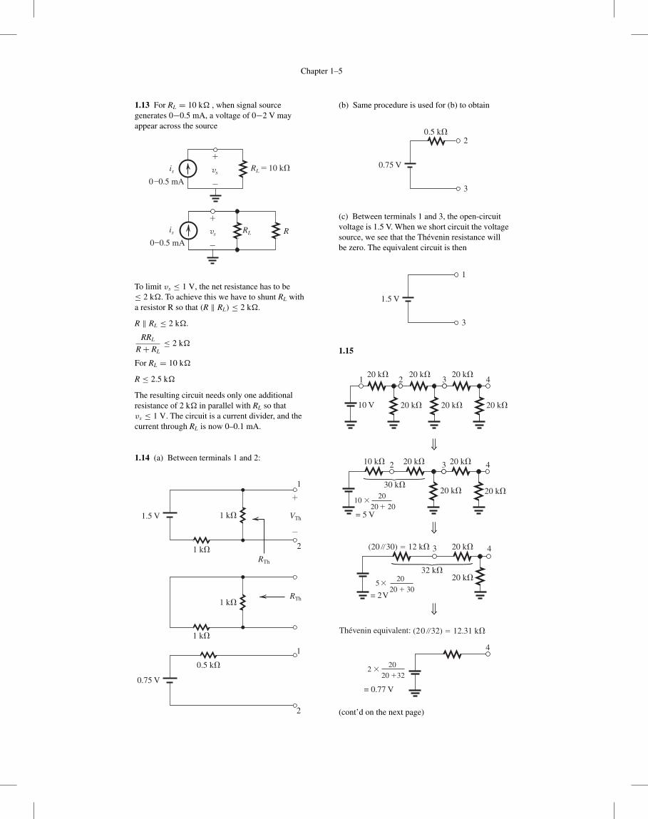
1.13 For RL = 10 k� , when signal sourcegenerates 0−0.5 mA, a voltage of 0−2 V mayappear across the source
R
0�0.5 mA
is vs
�
�
RL
To limit v s ≤ 1 V, the net resistance has to be≤ 2 k�. To achieve this we have to shunt RL witha resistor R so that (R ‖ RL) ≤ 2 k�.
R ‖ RL ≤ 2 k�.
RRL
R+ RL≤ 2 k�
For RL = 10 k�
R ≤ 2.5 k�
The resulting circuit needs only one additionalresistance of 2 k� in parallel with RL so thatvs ≤ 1 V. The circuit is a current divider, and thecurrent through RL is now 0–0.1 mA.
1.14 (a) Between terminals 1 and 2:
1.5 V VTh
RTh
RTh
2
1
2
1
1 k�
1 k�
1 k�
0.75 V
0.5 k�
�
�
1 k�
(b) Same procedure is used for (b) to obtain
0.75 V
2
3
0.5 k�
(c) Between terminals 1 and 3, the open-circuitvoltage is 1.5 V. When we short circuit the voltagesource, we see that the Thévenin resistance willbe zero. The equivalent circuit is then
1.5 V
1
3
1.15
(cont’d on the next page)
Chapter 1–6
3 k�
12.31 k�
0.77 V I
Now, when a resistance of 3 k� is connectedbetween node 4 and ground,
I = 0.77
12.31+ 3
= 0.05 mA
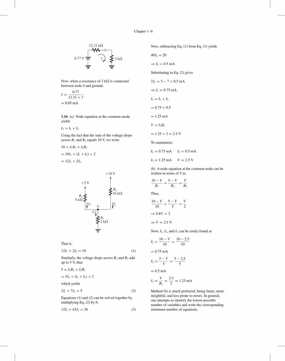
1.16 (a) Node equation at the common modeyields
I3 = I1 + I2
Using the fact that the sum of the voltage dropsacross R1 and R3 equals 10 V, we write
10 = I1R1 + I3R3
= 10I1 + (I1 + I2)× 2
= 12I1 + 2I2
�5 V
�10 V
5 k�
10 k�
2 k�
R2
R1
R3
I2 I1
I3
V
That is,
12I1 + 2I2 = 10 (1)
Similarly, the voltage drops across R2 and R3 addup to 5 V, thus
5 = I2R2 + I3R3
= 5I2 + (I1 + I2)× 2
which yields
2I1 + 7I2 = 5 (2)
Equations (1) and (2) can be solved together bymultiplying Eq. (2) by 6:
12I1 + 42I2 = 30 (3)
Now, subtracting Eq. (1) from Eq. (3) yields
40I2 = 20
⇒ I2 = 0.5 mA
Substituting in Eq. (2) gives
2I1 = 5− 7× 0.5 mA
⇒ I1 = 0.75 mA
I3 = I1 + I2
= 0.75+ 0.5
= 1.25 mA
V = I3R3
= 1.25× 2 = 2.5 V
To summarize:
I1 = 0.75 mA I2 = 0.5 mA
I3 = 1.25 mA V = 2.5 V
(b) A node equation at the common node can bewritten in terms of V as
10− V
R1+ 5− V
R2= V
R3
Thus,
10− V
10+ 5− V
5= V
2
⇒ 0.8V = 2
⇒ V = 2.5 V
Now, I1, I2, and I3 can be easily found as
I1 = 10− V
10= 10− 2.5
10
= 0.75 mA
I2 = 5− V
5= 5− 2.5
5
= 0.5 mA
I3 = V
R3= 2.5
2= 1.25 mA
Method (b) is much preferred, being faster, moreinsightful, and less prone to errors. In general,one attempts to identify the lowest possiblenumber of variables and write the correspondingminimum number of equations.
Chapter 1–7
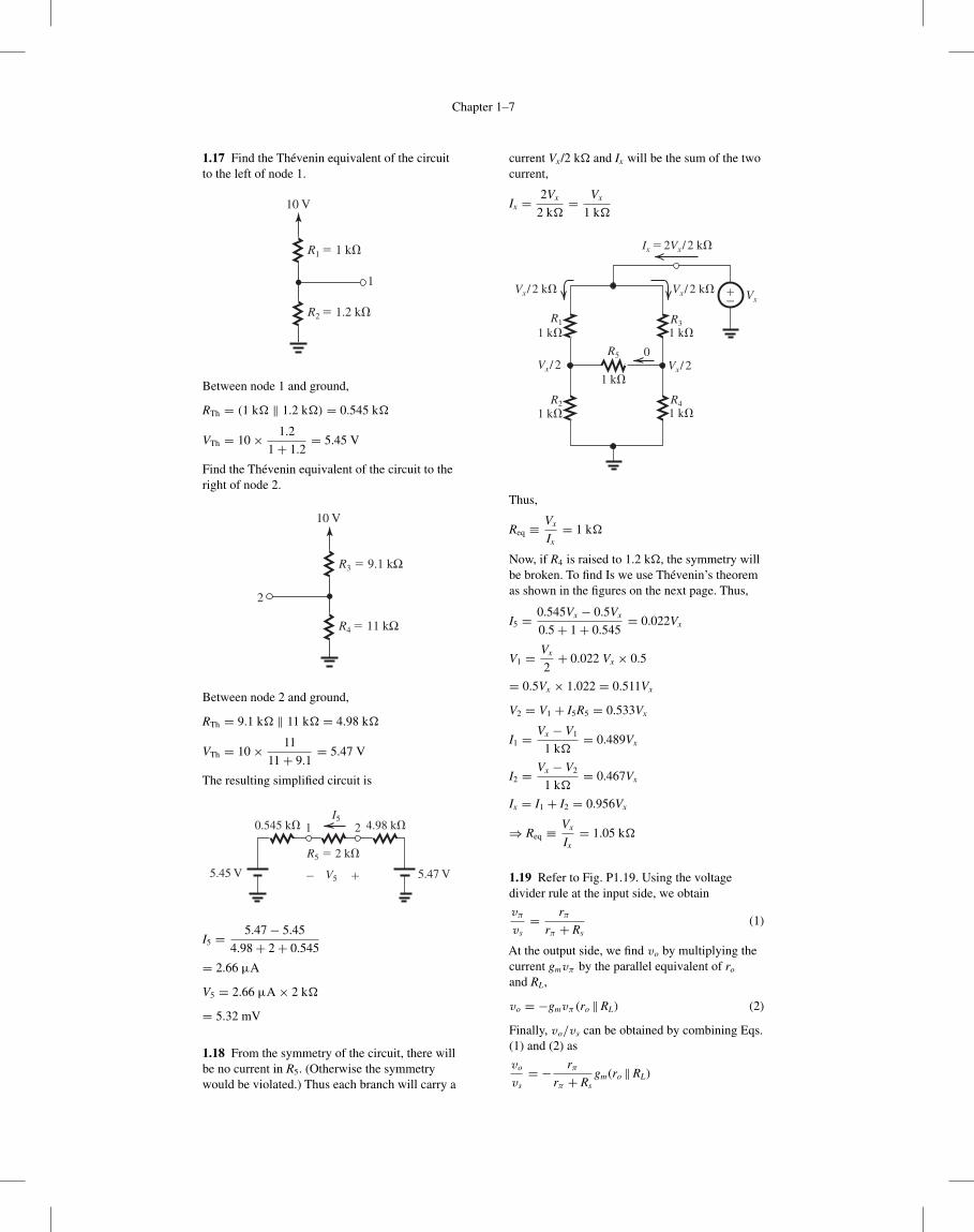
1.17 Find the Thévenin equivalent of the circuitto the left of node 1.
Between node 1 and ground,
RTh = (1 k� ‖ 1.2 k�) = 0.545 k�
VTh = 10× 1.2
1+ 1.2= 5.45 V
Find the Thévenin equivalent of the circuit to theright of node 2.
Between node 2 and ground,
RTh = 9.1 k� ‖ 11 k� = 4.98 k�
VTh = 10× 11
11+ 9.1= 5.47 V
The resulting simplified circuit is
R5 � 2 k�
V5
1 2
5.45 V 5.47 V
I50.545 k� 4.98 k�
� �
I5 = 5.47− 5.45
4.98+ 2+ 0.545
= 2.66 μA
V5 = 2.66 μA × 2 k�
= 5.32 mV
1.18 From the symmetry of the circuit, there willbe no current in R5. (Otherwise the symmetrywould be violated.) Thus each branch will carry a
current Vx/2 k� and Ix will be the sum of the twocurrent,
Ix = 2Vx
2 k�= Vx
1 k�
Thus,
Req ≡ Vx
Ix= 1 k�
Now, if R4 is raised to 1.2 k�, the symmetry willbe broken. To find Is we use Thévenin’s theoremas shown in the figures on the next page. Thus,
I5 = 0.545Vx − 0.5Vx
0.5+ 1+ 0.545= 0.022Vx
V1 = Vx
2+ 0.022 Vx × 0.5
= 0.5Vx × 1.022 = 0.511Vx
V2 = V1 + I5R5 = 0.533Vx
I1 = Vx − V1
1 k�= 0.489Vx
I2 = Vx − V2
1 k�= 0.467Vx
Ix = I1 + I2 = 0.956Vx
⇒ Req ≡ Vx
Ix= 1.05 k�
1.19 Refer to Fig. P1.19. Using the voltagedivider rule at the input side, we obtain
vπ
vs= rπ
rπ + Rs(1)
At the output side, we find vo by multiplying thecurrent gmvπ by the parallel equivalent of ro
and RL,
vo = −gmvπ (ro ‖RL) (2)
Finally, vo/vs can be obtained by combining Eqs.(1) and (2) as
vo
vs= − rπ
rπ + Rsgm(ro ‖RL)
Chapter 1–8
This figure belongs to Problem 1.18.
1.20 (a) T = 10−4 ms = 10−7 s
f = 1
T= 107 Hz
ω = 2π f = 6.28× 10⁷ rad/s
(b) f = 1 GHz = 109 Hz
T = 1
f= 10−9 s
ω = 2π f = 6.28× 10⁹ rad/s
(c) ω = 6.28× 10² rad/s
f = ω
2π= 102 Hz
T = 1
f= 10−2 s
(d) T = 10 s
f = 1
T= 10−1 Hz
ω = 2π f = 6.28× 10⁻¹ rad/s
(e) f = 60 Hz
T = 1
f= 1.67× 10⁻² s
ω = 2π f = 3.77× 10² rad/s
(f) ω = 1 krad/s = 103 rad/s
f = ω
2π= 1.59× 10² Hz
T = 1
f= 6.28× 10⁻³ s
(g) f = 1900 MHz = 1.9× 10⁹ Hz
T = 1
f= 5.26× 10⁻¹⁰ s
ω = 2π f = 1.194× 10¹⁰ rad/s
1.21 (a) Z = 1 k� at all frequencies
(b) Z = 1 /jωC = − j1
2π f × 10× 10−9
At f = 60 Hz, Z = − j265 k�
At f = 100 kHz, Z = − j159 �
At f = 1 GHz, Z = − j0.016 �
(c) Z = 1 /jωC = − j1
2π f × 10× 10−12
At f = 60 Hz, Z = − j0.265 G�
At f = 100 kHz, Z = − j0.16 M�
At f = 1 GHz, Z = − j15.9 �
(d) Z = jωL = j2π f L = j2π f × 10× 10−3
At f = 60 Hz, Z = j3.77 �
At f = 100 kHz, Z = j6.28 k�
At f = 1 GHz, Z = j62.8 M�
(e) Z = jωL = j2π f L = j2π f (1× 10⁻⁶)
f = 60 Hz, Z = j0.377 m�
f = 100 kHz, Z = j0.628 �
f = 1 GHz, Z = j6.28 k�
Chapter 1–9
1.22 (a) Z = R+ 1
jωC
= 103 + 1
j2π × 10× 103 × 10× 10−9
= (1− j1.59) k�
(b) Y = 1
R+ jωC
= 1
104 + j2π × 10× 103 × 0.01× 10−6
= 10−4(1+ j6.28) �
Z = 1
Y= 104
1+ j6.28
= 104(1− j6.28)
1+ 6.282
= (247.3− j1553) �
(c) Y = 1
R+ jωC
= 1
100× 103 + j2π × 10× 103 × 100× 10−12
= 10−5(1+ j0.628)
Z = 105
1+ j0.628
= (71.72− j45.04) k�
(d) Z = R+ jωL
= 100+ j2π × 10× 103 × 10× 10−3
= 100+ j6.28× 100
= (100+ j628), �
1.23
is
Rs
Rs��
vs
Théveninequivalent
Nortonequivalent
voc = vs
isc = is
vs = isRs
Thus,
Rs = voc
isc
(a) vs = voc = 1 V
is = isc = 0.1 mA
Rs = voc
isc= 1 V
0.1 mA= 10 k�
(b) vs = voc = 0.1 V
is = isc = 1 μA
Rs = voc
isc= 0.1 V
1 μA= 0.1 M� = 100 k�
1.24 The observed output voltage is 1 mV/ ◦C,which is one half the voltage specified by thesensor, presumably under open-circuit conditions:that is, without a load connected. It follows thatthat sensor internal resistance must be equal toRL, that is, 5 k�.
1.25
�
�
Rs
RL��
vs vo
vo
vs= RL
RL + Rs
vo = vs
/(1+ Rs
RL
)
Thus,vs
1+ Rs
100
= 40 (1)
andvs
1+ Rs
10
= 10 (2)
Dividing Eq. (1) by Eq. (2) gives
1+ (Rs /10)
1+ (Rs /100)= 4
⇒ RS = 50 k�
Substituting in Eq. (2) gives
vs = 60 mV
The Norton current is can be found as
is = vs
Rs= 60 mV
50 k�= 1.2 μA
1.26
�
�
��
vs vo Rs
Rs
io �
�
is vo
io
vo = vs − ioRs
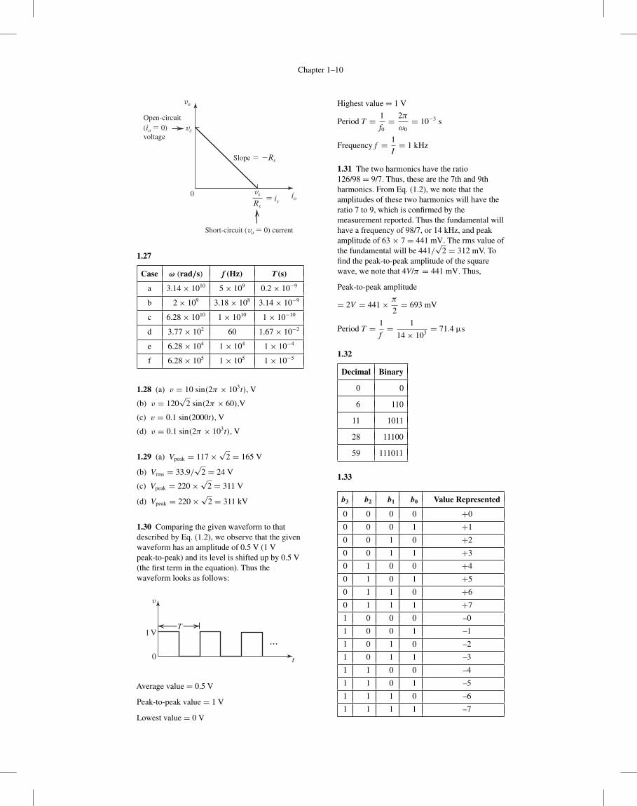
Chapter 1–10
Open-circuit(io � 0)voltage
0Rs
vs
vs
vo
� isio
Slope � �Rs
Short-circuit (vo � 0) current
1.27
Case ω (rad/s) f (Hz) T (s)
a 3.14× 10¹⁰ 5× 10⁹ 0.2× 10⁻⁹
b 2× 10⁹ 3.18× 10⁸ 3.14× 10⁻⁹
c 6.28× 10¹⁰ 1× 10¹⁰ 1× 10⁻¹⁰
d 3.77× 10² 60 1.67× 10⁻²
e 6.28× 10⁴ 1× 10⁴ 1× 10⁻⁴
f 6.28× 10⁵ 1× 10⁵ 1× 10⁻⁵
1.28 (a) v = 10 sin(2π × 103t), V
(b) v = 120√
2 sin(2π × 60),V
(c) v = 0.1 sin(2000t), V
(d) v = 0.1 sin(2π × 103t), V
1.29 (a) Vpeak = 117×√2 = 165 V
(b) Vrms = 33.9/√
2 = 24 V
(c) Vpeak = 220×√2 = 311 V
(d) Vpeak = 220×√2 = 311 kV
1.30 Comparing the given waveform to thatdescribed by Eq. (1.2), we observe that the givenwaveform has an amplitude of 0.5 V (1 Vpeak-to-peak) and its level is shifted up by 0.5 V(the first term in the equation). Thus thewaveform looks as follows:
v
T
t
1 V
0
...
Average value = 0.5 V
Peak-to-peak value = 1 V
Lowest value = 0 V
Highest value = 1 V
Period T = 1
f0= 2π
ω0= 10−3 s
Frequency f = 1
I= 1 kHz
1.31 The two harmonics have the ratio126/98 = 9/7. Thus, these are the 7th and 9thharmonics. From Eq. (1.2), we note that theamplitudes of these two harmonics will have theratio 7 to 9, which is confirmed by themeasurement reported. Thus the fundamental willhave a frequency of 98/7, or 14 kHz, and peakamplitude of 63 × 7 = 441 mV. The rms value ofthe fundamental will be 441/
√2 = 312 mV. To
find the peak-to-peak amplitude of the squarewave, we note that 4V/π = 441 mV. Thus,
Peak-to-peak amplitude
= 2V = 441× π
2= 693 mV
Period T = 1
f= 1
14× 103 = 71.4 μs
1.32
Decimal Binary
0 0
6 110
11 1011
28 11100
59 111011
1.33
b3 b2 b1 b0 Value Represented
0 0 0 0 +0
0 0 0 1 +1
0 0 1 0 +2
0 0 1 1 +3
0 1 0 0 +4
0 1 0 1 +5
0 1 1 0 +6
0 1 1 1 +7
1 0 0 0 –0
1 0 0 1 –1
1 0 1 0 –2
1 0 1 1 –3
1 1 0 0 –4
1 1 0 1 –5
1 1 1 0 –6
1 1 1 1 –7
Chapter 1–11
Note that there are two possible representations ofzero: 0000 and 1000. For a 0.5-V step size, analogsignals in the range ±3.5 V can be represented.
Input Steps Code
+2.5 V +5 0101
−3.0 V −6 1110
+2.7 +5 0101
−2.8 −6 1110
1.34 (a) For N bits there will be 2N possiblelevels, from 0 to VFS . Thus there will be (2N − 1)discrete steps from 0 to VFS with the step sizegiven by
Step size = VFS
2N − 1
This is the analog change corresponding to achange in the LSB. It is the value of the resolutionof the ADC.
(b) The maximum error in conversion occurswhen the analog signal value is at the middle of astep. Thus the maximum error is
Step
1
2× step size = 1
2
VFS
2N − 1
This is known as the quantization error.
(c)5 V
2N − 1≤ 2 mV
2N − 1 ≥ 2500
2N ≥ 2501⇒ N = 12,
For N = 12,
Resolution = 5
212 − 1= 1.2 mV
Quantization error = 1.2
2= 0.6 mV
1.35 (a) When bi = 1, the ith switch is inposition 1 and a current (Vref /2iR) flows to theoutput. Thus iO will be the sum of all the currentscorresponding to “1” bits, that is,
iO = Vref
R
(b1
21+ b2
22+ · · · + bN
2N
)
(b) bN is the LSB
b1 is the MSB
(c) iOmax = 10 V
10 k�
(1
21+ 1
22+ 1
23+ 1
24
+ 1
25+ 1
26+ 1
27+ 1
28
)
= 0.99609375 mA
Corresponding to the LSB changing from 0 to 1the output changes by (10/10)× 1/28 =3.91 μA.
1.36 There will be 44,100 samples per secondwith each sample represented by 16 bits. Thus thethroughput or speed will be 44, 100× 16 =7.056× 105 bits per second.
1.37 (a) Av = vO
v I= 10 V
100 mV= 100 V/V
or 20 log 100 = 40 dB
Ai = iO
iI= vO/RL
iI= 10 V/100 �
100 μA= 0.1 A
100 μA
= 1000 A/A
or 20 log 1000 = 60 dB
Ap = vOiO
v I iI= vO
v I× iO
iI= 100× 1000
= 105 W/W
or 10 log 105 = 50 dB
(b) Av = vO
v I= 1 V
10 μV= 1× 10⁵ V/V
or 20 log 1× 105 = 100 dB
Ai = iO
iI= vO/RL
iI= 1 V/10 k�
100 nA
=0.1 mA
100 nA= 0.1× 10⁻³
100× 10−9 = 1000 A/A
or 20 log Ai = 60 dB
Ap = vOiO
v I iI= vO
v I× iO
iI
= 1× 105 × 1000
= 1× 10⁸ W/W
or 10 log AP = 80 dB
(c) Av = vO
v i= 5 V
1 V= 5 V/V
or 20 log 5 = 14 dB
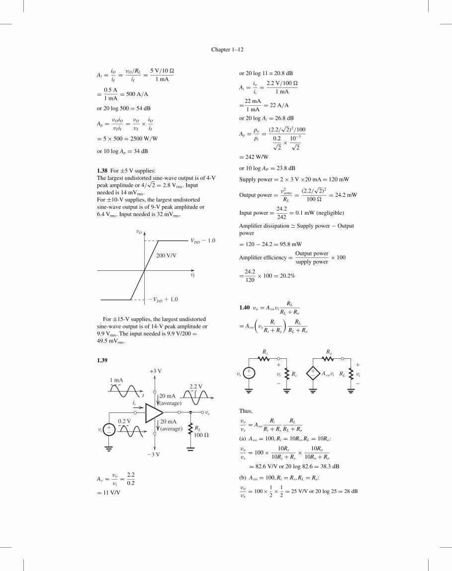
Chapter 1–12
Ai = iO
iI= vO/RL
iI= 5 V/10 �
1 mA
= 0.5 A
1 mA= 500 A/A
or 20 log 500 = 54 dB
Ap = vOiO
v I iI= vO
v I× iO
iI
= 5× 500 = 2500 W/W
or 10 log Ap = 34 dB
1.38 For ±5 V supplies:The largest undistorted sine-wave output is of 4-Vpeak amplitude or 4/
√2 = 2.8 Vrms. Input
needed is 14 mVrms.For ±10-V supplies, the largest undistortedsine-wave output is of 9-V peak amplitude or6.4 Vrms. Input needed is 32 mVrms.
vO
vI
200 V/V
VDD � 1.0
�VDD � 1.0
For ±15-V supplies, the largest undistortedsine-wave output is of 14-V peak amplitude or9.9 Vrms. The input needed is 9.9 V/200 =49.5 mVrms.
1.39
0.2 V
2.2 V
+3 V
�3 V
��
vo
t
1 mA
20 mA(average)
20 mA(average)
100 �
ii
RLvi
Av = vo
v i= 2.2
0.2
= 11 V/V
or 20 log 11 = 20.8 dB
Ai = io
ii= 2.2 V/100 �
1 mA
=22 mA
1 mA= 22 A/A
or 20 log Ai = 26.8 dB
Ap = po
pi= (2.2/
√2)2/100
0.2√2× 10⁻³
√2
= 242 W/W
or 10 log AP = 23.8 dB
Supply power = 2× 3 V×20 mA= 120 mW
Output power = v2orms
RL= (2.2/
√2)2
100 �= 24.2 mW
Input power = 24.2
242= 0.1 mW (negligible)
Amplifier dissipation Supply power − Outputpower
= 120 − 24.2 = 95.8 mW
Amplifier efficiency = Output power
supply power× 100
=24.2
120× 100 = 20.2%
1.40 vo = Avov iRL
RL + Ro
= Avo
(vs
Ri
Ri + Rs
)RL
RL + Ro
�
�
�� vi
�
�
vivs Ri
Rs
�� RLAv ovi
Ro
Thus,
vo
vs= Avo
Ri
Ri + Rs
RL
RL + Ro
(a) Avo = 100, Ri = 10Rs, RL = 10Ro:
vo
vs= 100× 10Rs
10Rs + Rs× 10Ro
10Ro + Ro
= 82.6 V/V or 20 log 82.6 = 38.3 dB
(b) Avo = 100, Ri = Rs, RL = Ro:
vo
vs= 100× 1
2× 1
2= 25 V/V or 20 log 25 = 28 dB
Chapter 1–13
(c) Avo = 100 V/V, Ri = Rs/10, RL = Ro/10:
vo
vs= 100
Rs/10
(Rs/10)+ Rs
Ro/10
(Ro/10)+ Ro
= 0.826 V/V or 20 log 0.826 = −1.7 dB
1.41
�
�
�
�
��vi vo
100 �
500 �1 M� 100vi
20 log Avo = 40 dB⇒ Avo = 100 V/V
Av = vo
v i
= 100× 500
500+ 100
= 83.3 V/V
or 20 log 83.3 = 38.4 dB
Ap = v2o/500 �
v2i /1 M�
= A2v × 104 = 1.39× 10⁷ W/W
or 10 log (1.39× 10⁷) = 71.4 dB.
For a peak output sine-wave current of 20 mA,the peak output voltage will be 20 mA× 500 �
= 10 V. Correspondingly v i will be a sine wavewith a peak value of 10 V/Av = 10/83.3, or anrms value of 10/(83.3×√2) = 0.085 V.Corresponding output power = (10/
√2)2/500 �
= 0.1 W
1.42
�
�
�
�
��
��vi vovs Ri RL
RoRs
Av ovi
vo
vs= 10 k�
10 k�+ 100 k�× 1000× 100 �
100 �+ 1 k�
= 10
110× 1000× 100
1100= 8.26 V/V
The signal loses about 90% of its strength whenconnected to the amplifier input (becauseRi = Rs/10). Also, the output signal of theamplifier loses approximately 90% of its strengthwhen the load is connected (because RL = Ro/10).Not a good design! Nevertheless, if the sourcewere connected directly to the load,
vo
vs= RL
RL + Rs
= 100 �
100 �+ 100 k�
0.001 V/V
vs
�
�
��
vo
Rs � 100 k�
RL
100 �
which is clearly a much worse situation. Indeedinserting the amplifier increases the gain by afactor 8.3/0.001 = 8300.
1.43
�
�
�� vi
200 k�
1 M�1 V�
�
��
vo
20 �
100 �1�vi
vo = 1 V × 1 M�
1 M�+ 200 k�
× 1× 100 �
100 �+ 20 �
= 1
1.2× 100
120= 0.69 V
Voltage gain = vo
vs= 0.69 V/V or −3.2 dB
Current gain = vo/100 �
vs/1.2 M�= 0.69× 1.2× 104
= 8280 A/A or 78.4 dB
Power gain = v2o/100 �
v2s /1.2 M�
= 5713 W/W
or 10 log 5713 = 37.6 dB
(This takes into account the power dissipated inthe internal resistance of the source.)
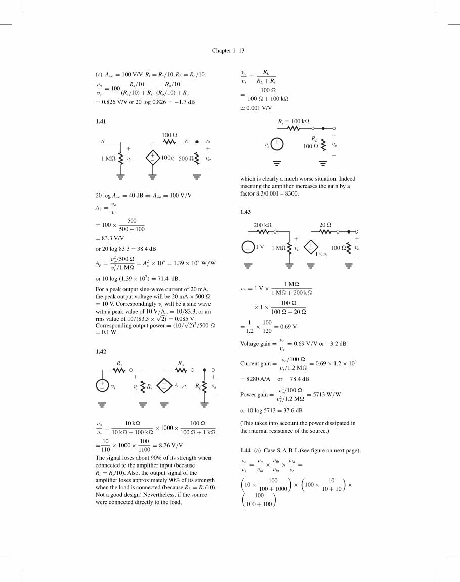
1.44 (a) Case S-A-B-L (see figure on next page):
vo
vs= vo
v ib× v ib
v ia× v ia
vs=
(10× 100
100+ 1000
)×(
100× 10
10+ 10
)×(
100
100+ 100
)
Chapter 1–14
This figure belongs to 1.44, part (a).
This figure belongs to 1.44, part (b).
This figure belongs to Problem 1.45.
vo
vs= 22.7 V/V and gain in dB 20 log 22.7 =
27.1 dB
(b) Case S-B-A-L (see figure above):
vo
vs= vo
v ia· v ia
v ib· v ib
vs
=(
100× 100
100+ 10 K
)×(
10× 100 K
100 K + 1 K
)×
(10 K
10 K + 100 K
)
vo
vs= 0.89 V/V and gain in dB is 20 log 0.89 =
−1 dB. Obviously, case a is preferred because itprovides higher voltage gain.
1.45 In Example 1.3, when the first and thesecond stages are interchanged, the circuit lookslike the figure above, and
v i1
vs= 100 k�
100 k�+ 100 k�= 0.5 V/V
Av1 = v i2
v i1= 100× 1 M�
1 M�+ 1 k�
= 99.9 V/V
Av2 = v i3
v i2= 10× 10 k�
10 k�+ 1 k�
= 9.09 V/V
Av3 = vL
v i3= 1× 100 �
100 �+ 10 �= 0.909 V/V
Total gain = Av = vL
v i1= Av1 × Av2 × Av3
= 99.9 × 9.09 × 0.909 = 825.5 V/V
The voltage gain from source to load is
vL
vs= vL
v i1× v i1
vS= Av · v i1
vS
= 825.5× 0.5
= 412.7 V/V
The overall voltage has reduced appreciably. Thisis because the input resistance of the first stage,Rin, is comparable to the source resistance Rs. InExample 1.3 the input resistance of the first stageis much larger than the source resistance.
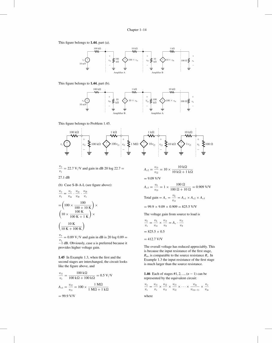
1.46 Each of stages #1, 2, ..., (n− 1) can berepresented by the equivalent circuit:
vo
vs= v i1
vs× v i2
v i1× v i3
v i2× · · · × v in
v i(n−1)
× vo
v in
where
Chapter 1–15
This figure belongs to 1.46.
��
Rs � 10 k�
200 �
Ri1 � 10 k� Ron � 1 k�
5 mV
vs
#1 #2 #n
vi1
�
�
vi2
�
�
vin
�
�
vo
�
�RL
10 k�
1 k�
10 k�
#m
Ri(m �1)
vi(m �1)
�
�
vim
�
�
vi(m �1)10vim
�
�
vim
�
�
��
v i1
vs= 10 k�
10 k�+ 10 k�= 0.5 V/V
vo
v in= 10× 200 �
1 k�+ 200 �= 1.67 V/V
v i2
v i1= v i3
v i2= · · · = v in
v i(n−1)
= 10× 10 k�
10 k�+ 10 k�
= 9.09 V/V
Thus,
vo
vs= 0.5× (9.09)n−1× 1.67 = 0.833× (9.09)n−1
For vs = 5 mV and vo = 3 V, the gainvo
vsmust be
≥ 600, thus
0.833× (9.09)n−1 ≥ 600
⇒ n = 4
Thus four amplifier stages are needed, resulting in
vo
vs= 0.833× (9.09)3 = 625.7 V/V
and correspondingly
vo = 625.7× 5 mV = 3.13 V
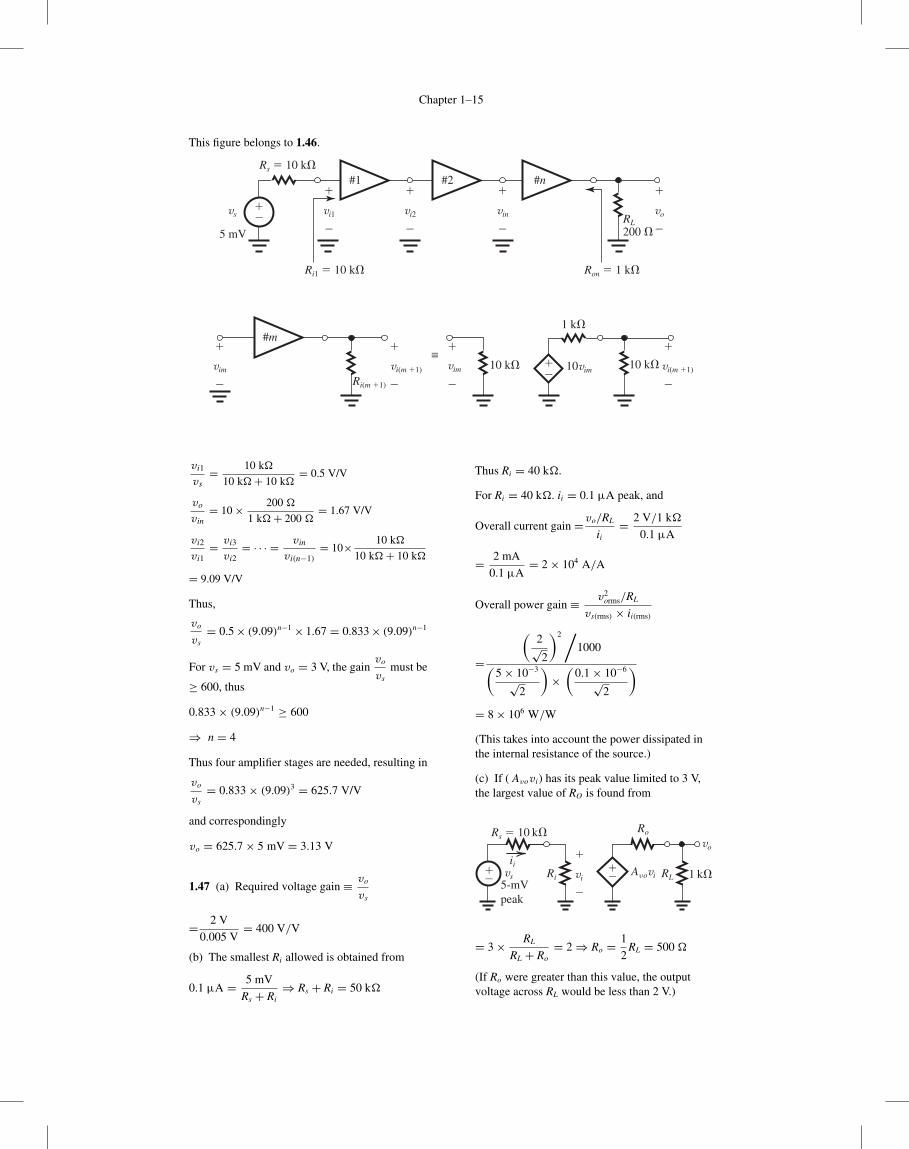
1.47 (a) Required voltage gain ≡ vo
vs
= 2 V
0.005 V= 400 V/V
(b) The smallest Ri allowed is obtained from
0.1 μA = 5 mV
Rs + Ri⇒ Rs + Ri = 50 k�
Thus Ri = 40 k�.
For Ri = 40 k�. ii = 0.1 μA peak, and
Overall current gain =vo/RL
ii= 2 V/1 k�
0.1 μA
= 2 mA
0.1 μA= 2× 10⁴ A/A
Overall power gain ≡ v2orms/RL
vs(rms) × ii(rms)
=
(2√2
)2 /1000(
5× 10⁻³
√2
)×(
0.1× 10⁻⁶
√2
)
= 8× 10⁶ W/W
(This takes into account the power dissipated inthe internal resistance of the source.)
(c) If ( Avov i) has its peak value limited to 3 V,the largest value of RO is found from
Rs � 10 k�
��
�
�
vs vi
vo
iiRi
5-mVpeak
Ro
RL�� Avovi 1 k�
= 3× RL
RL + Ro= 2⇒ Ro = 1
2RL = 500 �
(If Ro were greater than this value, the outputvoltage across RL would be less than 2 V.)
Chapter 1–16
This figure belongs to 1.48.
�
�
vi1
�
�
vi2
�
�
vi3
�
�
vo100 �
20 �1 k�10 k�0.5 M�
10 k�
100vi2 1vi310vi1
1 M�30 mVrms
10 k���
��
��
∼
(d) For Ri = 40 k� and Ro = 500 �, therequired value Avo can be found from
400 V/V = 40
40+ 10× Avo × 1
1+ 0.5
⇒ Avo = 750 V/V
(e) Ri = 100 k�(1× 10⁵ �)
Ro = 100 �(1× 10² �)
400 = 100
100+ 10× Avo × 1000
1000+ 100
⇒ Avo = 484 V/V
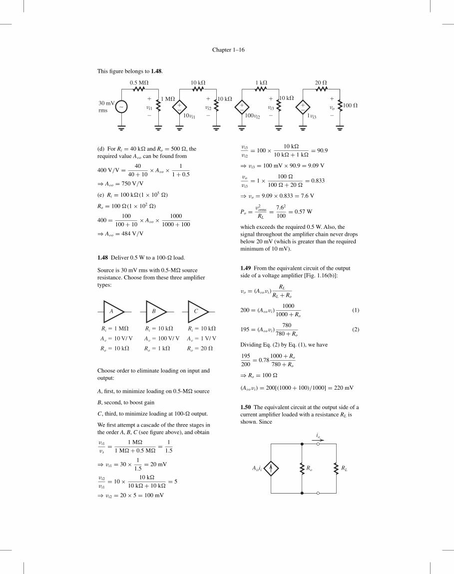
1.48 Deliver 0.5 W to a 100-� load.
Source is 30 mV rms with 0.5-M� sourceresistance. Choose from these three amplifiertypes:
A B C
Ri � 1 M�
Av � 10 V/ V
Ro � 10 k�
Ri � 10 k�
Av � 100 V/ V
Ro � 1 k�
Ri � 10 k�
Av � 1 V/ V
Ro � 20 �
Choose order to eliminate loading on input andoutput:
A, first, to minimize loading on 0.5-M� source
B, second, to boost gain
C, third, to minimize loading at 100-� output.
We first attempt a cascade of the three stages inthe order A, B, C (see figure above), and obtain
v i1
vs= 1 M�
1 M�+ 0.5 M�= 1
1.5
⇒ v i1 = 30× 1
1.5= 20 mV
v i2
v i1= 10× 10 k�
10 k�+ 10 k�= 5
⇒ v i2 = 20× 5 = 100 mV
v i3
v i2= 100× 10 k�
10 k�+ 1 k�= 90.9
⇒ v i3 = 100 mV× 90.9 = 9.09 V
vo
v i3= 1× 100 �
100 �+ 20 �= 0.833
⇒ vo = 9.09× 0.833 = 7.6 V
Po = v2orms
RL= 7.62
100= 0.57 W
which exceeds the required 0.5 W. Also, thesignal throughout the amplifier chain never dropsbelow 20 mV (which is greater than the requiredminimum of 10 mV).
1.49 From the equivalent circuit of the outputside of a voltage amplifier [Fig. 1.16(b)]:
vo = (Avov i)RL
RL + Ro
200 = (Avov i)1000
1000+ Ro(1)
195 = (Avov i)780
780+ Ro(2)
Dividing Eq. (2) by Eq. (1), we have
195
200= 0.78
1000+ Ro
780+ Ro
⇒ Ro = 100 �
(Avov i) = 200[(1000+ 100)/1000] = 220 mV
1.50 The equivalent circuit at the output side of acurrent amplifier loaded with a resistance RL isshown. Since
RLRoAisii
io
Chapter 1–17
io = (Aisii)Ro
Ro + RL
we can write
1 = (Aisii)Ro
Ro + 1(1)
and
0.5 = (Aisii)Ro
Ro + 12(2)
Dividing Eq. (1) by Eq. (2), we have
2 = Ro + 12
Ro + 1⇒ Ro = 10 k�
Aisii = 1× 10+ 1
10= 1.1 mA
1.51
Rs � 1 k�
��
�
�
vs viRi
Gmvi vo
RLRo
�
�2 k�
Gm = 60 mA/V
Ro = 20 k�
RL = 1 k�
v i = vsRi
Rs + Ri
= vs2
1+ 2= 2
3v s
vo = Gmv i(RL ‖ Ro)
= 6020× 1
20+ 1v i
= 6020
21× 2
3v s
Overall voltage gain ≡ vo
vs= 38.1 V/V
1.52
�
�
vi gmviRi
i1
i2ix
vx��
ix = i1 + i2
i1 = v i/Ri
i2 = gmv i
v i = vx
⎫⎪⎪⎪⎪⎪⎪⎬⎪⎪⎪⎪⎪⎪⎭
ix = vx/Ri + gmvx
ix = vx
(1
Ri+ gm
)vx
ix= 1
1/Ri + gm
= Ri
1+ gmRi= Rin
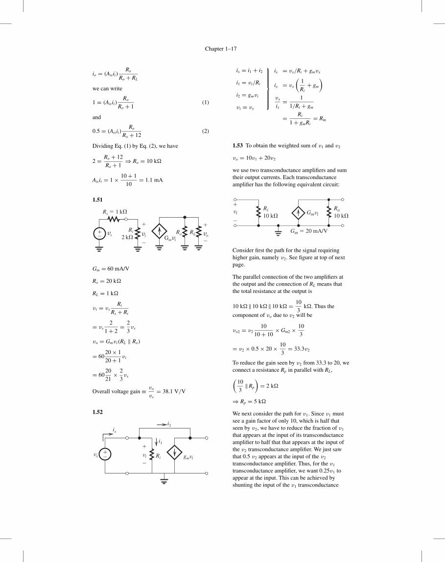
1.53 To obtain the weighted sum of v1 and v2
vo = 10v1 + 20v2
we use two transconductance amplifiers and sumtheir output currents. Each transconductanceamplifier has the following equivalent circuit:
Ri10 k�
RoGmvi
Gm � 20 mA/V
10 k�vi
�
�
Consider first the path for the signal requiringhigher gain, namely v2. See figure at top of nextpage.
The parallel connection of the two amplifiers atthe output and the connection of RL means thatthe total resistance at the output is
10 k� ‖ 10 k� ‖ 10 k� = 10
3k�. Thus the
component of vo due to v2 will be
vo2 = v210
10+ 10× Gm2 × 10
3
= v2 × 0.5× 20× 10
3= 33.3v2
To reduce the gain seen by v2 from 33.3 to 20, weconnect a resistance Rp in parallel with RL,(
10
3‖Rp
)= 2 k�
⇒ Rp = 5 k�
We next consider the path for v1. Since v1 mustsee a gain factor of only 10, which is half thatseen by v2, we have to reduce the fraction of v1
that appears at the input of its transconductanceamplifier to half that that appears at the input ofthe v2 transconductance amplifier. We just sawthat 0.5 v2 appears at the input of the v2
transconductance amplifier. Thus, for the v1
transconductance amplifier, we want 0.25v1 toappear at the input. This can be achieved byshunting the input of the v1 transconductance
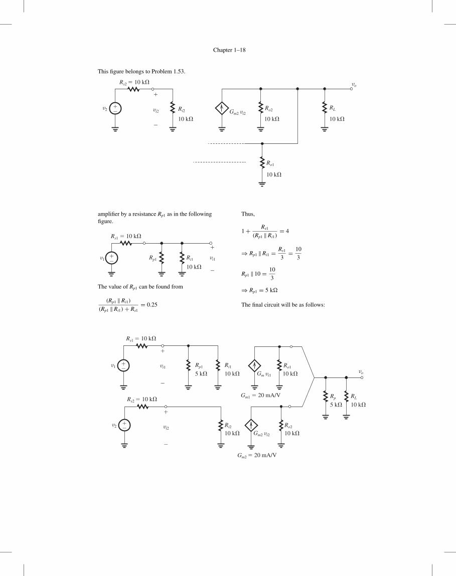
Chapter 1–18
This figure belongs to Problem 1.53.
amplifier by a resistance Rp1 as in the followingfigure.
v1
Rs1 � 10 k�
vi1
�
�
Rp1 Ri1
10 k�
��
The value of Rp1 can be found from
(Rp1 ‖Ri1)
(Rp1 ‖Ri1)+ Rs1= 0.25
Thus,
1+ Rs1
(Rp1 ‖Ri1)= 4
⇒ Rp1 ‖Ri1 = Rs1
3= 10
3
Rp1 ‖ 10 = 10
3
⇒ Rp1 = 5 k�
The final circuit will be as follows:
Chapter 1–19
1.54 Voltage amplifier:
vi voRi
Rs
Ro1 to 10 k�
RL
1 k� to10 k�
Avo vi
��
�
�
�
�
��
io
vs
For Rs varying in the range 1 k� to 10 k� and�vo limited to 10%, select Ri to be sufficientlylarge:
Ri ≥ 10 Rsmax
Ri = 10× 10 k� = 100 k� = 1× 10⁵ �
For RL varying in the range 1 k� to 10 k�, theload voltage variation limited to 10%, select Ro
sufficiently low:
Ro ≤ RLmin
10
Ro = 1 k�
10= 100 � = 1× 10² �
Now find Avo:
vomin = 10 mV × Ri
Ri + Rsmax× Avo
RLmin
Ro + RLmin
1 = 10× 10−3 × 100 k�
100 k�+ 10 k�
×Avo × 1 k�
100 �+ 1 k�
⇒ Avo = 121 V/V
vo
Ro
Avovi��
�
�
�
�
vi Ri
Values for the voltage amplifier equivalentcircuit are
Ri = 1× 10⁵ �, Avo = 121 V/V, and
Ro = 1× 10² �
1.55 Current amplifier:
Rs
1 k to10 k�
RoRL
1 k to10 k�
10 �A
Ais ii
Ri
ii
is
io
For Rs varying in the range 1 k� to 10 k� andload current variation limited to 10%, select Ri tobe sufficiently low:
Ri ≤ Rsmin
10
Ri = 1 k�
10= 100 � = 1× 10² �
For RL varying in the range 1 k� to 10 k� andthe load current variation limited to 10%, Ro isselected sufficiently large:
Ro ≥ 10 RLmax
Ro = 10× 10 k�
= 100 k� = 1× 10⁵ �
Now we find Ais:
iomin = 10 μA × Rsmin
Rsmin + Ri× Ais × Ro
Ro + RLmax
1× 10−3 = 10× 10−6 1 k�
1 k�+ 100 �
× Ais100 k�
100 k�+ 10 k�
⇒ Ais = 121 A/A
Current amplifier equivalent circuit:
RoAis iiRi
ii
io
Ri = 1× 10² �, Ais = 121 A/A,
Ro = 1× 10⁵ �
1.56 Transconductance amplifier:
��
�
�
vs viRi
Rs
Gmvi
RL
Ro
io
1 to10 k�
1 to 10 k�
10 mVnominal
Chapter 1–20
For Rs varying in the range 1 to 10 k�, and �io
limited to 10%, we have to select Ri sufficientlylarge;
Ri ≥ 10Rsmax
Ri = 100 k� = 1× 10⁵ �
For RL varying in the range 1 to 10 k�, thechange in io can be kept to 10% if Ro is selectedsufficiently large;
Ro ≥ RLmax
Thus Ro = 100 k� = 1× 10⁵ �
For vs = 10 mV,
iomin = 10−2 Ri
Ri + RsmaxGm
Ro
Ro + RLmax
10−3 = 10−2 100
100+ 10Gm
100
100+ 10
Gm = 1.21× 10⁻¹ A/V
= 121 mA/V
Gmvi
Gm �121 mA/V
�
�
vi
In Out
100 k� 100 k�
1.57 Ro = Open-circuit output voltage
Short-circuit output current= 10 V
5 mA= 2 k�
vo = 10× 2
2+ 2= 5 V
Av = vo
v i= 10(2/4)
1× 10−6 × (200 ‖ 5)× 103
1025 V/V or 60.2 dB
Ai = io
ii= vo/RL
v i/Ri
= vo
v i
Ri
RL= 1025× 5 k�
2 k�
= 2562.5 A/A or 62.8 dB
The overall current gain can be found as
io
is= vo/RL
1 μA= 5 V/2 k�
1 μA
= 2.5 mA
1 μA= 2500 A/A
or 68 dB.
Ap = v2o/RL
i2i Ri= 52/(2× 103)(
10−6 × 200
200+ 5
)2
5× 103
= 2.63× 10⁶ W/W or 64.2 dB
1.58
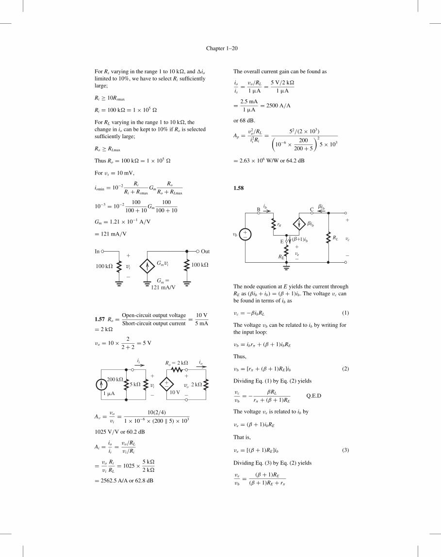
The node equation at E yields the current throughRE as (βib + ib) = (β + 1)ib. The voltage vc canbe found in terms of ib as
vc = −βibRL (1)
The voltage vb can be related to ib by writing forthe input loop:
vb = ibrπ + (β + 1)ibRE
Thus,
vb = [rπ + (β + 1)RE]ib (2)
Dividing Eq. (1) by Eq. (2) yields
vc
vb= − βRL
rπ + (β + 1)REQ.E.D
The voltage ve is related to ib by
ve = (β + 1)ibRE
That is,
ve = [(β + 1)RE]ib (3)
Dividing Eq. (3) by Eq. (2) yields
ve
vb= (β + 1)RE
(β + 1)RE + rπ
Chapter 1–21
Dividing the numerator and denominator by(β + 1) gives
ve
vb= RE
RE + [rπ/(β + 1)] Q.E.D
1.59
R
�
�
v1gmv1
gm � 100 mA/V
R � 5 k�
gmv2
�
�
v2
io
vo
io = gmv1 − gmv2
vo = ioRL = gmR(v1 − v2)
v1 = v2 = 1 V ∴ vo = 0 V
v1 = 1.01 Vv2 = 0.99 V
}∴ vo = 100× 5× 0.02 = 10 V
1.60
I1
V1
g12I2
1/g11
�
�
g21V1
g22
�� V2
I2
�
�
I1
V2
I2
AvoV1V1 Ri
Ro
�
�
��
�
�
The correspondences between the current andvoltage variables are indicated by comparing thetwo equivalent-circuit models above. At theoutset we observe that at the input side of theg-parameter model, we have the controlledcurrent source g12I2. This has no correspondencein the equivalent-circuit model of Fig. 1.16(a). Itrepresents internal feedback, internal to the
amplifier circuit. In developing the model ofFig. 1.16(a), we assumed that the amplifier isunilateral (i.e., has no internal feedback, or thatthe input side does not know what happens at theoutput side). If we neglect this internal feedback,that is, assume g12 = 0, we can compare the twomodels and thus obtain:
Ri = 1/g11
Avo = g21
Ro = g22
1.61 Circuits of Fig. 1.22:
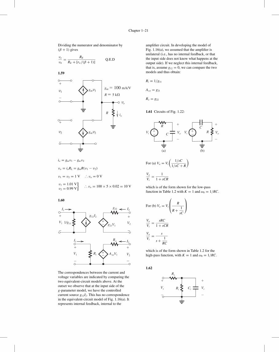
�
�
Vi Vo
R
C
(a) (b)
��
�
�
Vi Vo
CR�
�
For (a) Vo = Vi
(1/sC
1/sC + R
)
Vo
Vi= 1
1+ sCR
which is of the form shown for the low-passfunction in Table 1.2 with K = 1 and ω0 = 1/RC.
For (b) Vo = Vi
⎛⎜⎝ R
R+ 1
sC
⎞⎟⎠
Vo
Vi= sRC
1+ sCR
Vo
Vi= s
s+ 1
RC
which is of the form shown in Table 1.2 for thehigh-pass function, with K = 1 and ω0 = 1/RC.
1.62
�
�
Vi
�
�
Rs
RiVs Ci
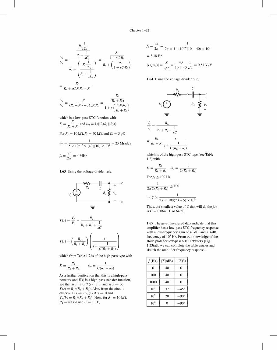
Chapter 1–22
Vi
Vs=
Ri1
sCi
Ri + 1
sCi
Rs +
⎛⎜⎜⎝
Ri1
sCi
Ri + 1
sCi
⎞⎟⎟⎠=
Ri
1+ sCiRi
Rs +(
Ri
1+ sCiRi
)
= Ri
Rs + sCiRiRs + Ri
Vi
Vs= Ri
(Rs + Ri)+ sCiRiRs=
Ri
(Rs + Ri)
1+ s
(CiRiRs
Rs + Ri
)
which is a low-pass STC function with
K = Ri
Rs + Riand ω0 = 1/[Ci(Ri ‖Rs)].
For Rs = 10 k�, Ri = 40 k�, and Ci = 5 pF,
ω0 = 1
5× 10−12 × (40 ‖ 10)× 103= 25 Mrad/s
f0 = 25
2π= 4 MHz
1.63 Using the voltage-divider rule.
�
�
VoVi
R1
R2
C��
T (s) = Vo
Vi= R2
R2 + R1 + 1
sC
T (s) =(
R2
R1 + R2
)⎛⎜⎜⎝ s
s+ 1
C(R1 + R2)
⎞⎟⎟⎠
which from Table 1.2 is of the high-pass type with
K = R2
R1 + R2ω0 = 1
C(R1 + R2)
As a further verification that this is a high-passnetwork and T(s) is a high-pass transfer function,see that as s⇒ 0, T (s)⇒ 0; and as s→∞,T (s) = R2/(R1 + R2). Also, from the circuit,observe as s→∞, (1/sC)→ 0 andVo/Vi = R2/(R1 + R2). Now, for R1 = 10 k�,R2 = 40 k� and C = 1 μF,
f0 = ω0
2π= 1
2π × 1× 10−6(10+ 40)× 103
= 3.18 Hz
|T (jω0)| = K√2= 40
10+ 40
1√2= 0.57 V/V
1.64 Using the voltage divider rule,
RL
RsC
VlVs
�
�
��
Vl
Vs= RL
RL + Rs + 1
sC
= RL
RL + Rs
s
s+ 1
C(RL + Rs)
which is of the high-pass STC type (see Table1.2) with
K = RL
RL + Rsω0 = 1
C(RL + Rs)
For f0 ≤ 100 Hz
1
2πC(RL + Rs)≤ 100
⇒ C ≥ 1
2π × 100(20+ 5)× 103
Thus, the smallest value of C that will do the jobis C = 0.064 μF or 64 nF.
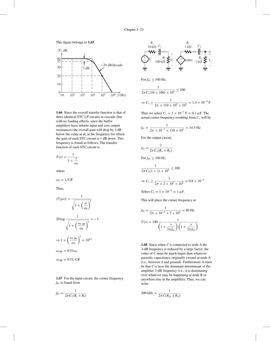
1.65 The given measured data indicate that thisamplifier has a low-pass STC frequency responsewith a low-frequency gain of 40 dB, and a 3-dBfrequency of 104 Hz. From our knowledge of theBode plots for low-pass STC networks [Fig.1.23(a)], we can complete the table entries andsketch the amplifier frequency response.
f (Hz) |T |(dB) ∠T(◦)
0 40 0
100 40 0
1000 40 0
104 37 −45◦
105 20 −90◦
106 0 −90◦
Chapter 1–23
This figure belongs to 1.65.
f (Hz)
�20 dB/decade3 dB
100
10
20
30
3740
T , dB
102 103 104 105 106
1.66 Since the overall transfer function is that ofthree identical STC LP circuits in cascade (butwith no loading effects, since the bufferamplifiers have infinite input and zero outputresistances) the overall gain will drop by 3 dBbelow the value at dc at the frequency for whichthe gain of each STC circuit is 1 dB down. Thisfrequency is found as follows: The transferfunction of each STC circuit is
T (s) = 1
1+ s
ω0
where
ω0 = 1/CR
Thus,
|T (jω)| = 1√1+
(ω
ω0
)2
20 log1√
1+(
ω1 dB
ω0
)2= −1
⇒ 1+(
ω1 dB
ω0
)2
= 100,1
ω1dB = 0.51ω0
ω1dB = 0.51/CR
1.67 For the input circuit, the corner frequencyf01 is found from
f01 = 1
2πC1(Rs + Ri)
��
�
�
�
�
V VR
100 k� 100V
R10 k� C
VR
1 k�
R1 k� C
��
For f01 ≤ 100 Hz,
1
2πC1(10+ 100)× 103 ≤ 100
⇒ C1 ≥ 1
2π × 110× 103 × 102 = 1.4× 10⁻⁸ F
Thus we select C1 = 1× 10⁻⁷ F = 0.1 μF. Theactual corner frequency resulting from C1 will be
f01 = 1
2π × 10−7 × 110× 103 = 14.5 Hz
For the output circuit,
f02 = 1
2πC2(Ro + RL)
For f02 ≤ 100 Hz,
1
2πC2(1+ 1)× 103 ≤ 100
⇒ C2 ≥ 1
2π × 2× 103 × 102 = 0.8× 10⁻⁶
Select C2 = 1× 10−6 = 1 μF.
This will place the corner frequency at
f02 = 1
2π × 10−6 × 2× 103 = 80 Hz
T (s) = 100s(
1+ s
2π f01
)(1+ s
2π f02
)
1.68 Since when C is connected to node A the3-dB frequency is reduced by a large factor, thevalue of C must be much larger than whateverparasitic capacitance originally existed at node A(i.e., between A and ground). Furthermore, it mustbe that C is now the dominant determinant of theamplifier 3-dB frequency (i.e., it is dominatingover whatever may be happening at node B oranywhere else in the amplifier). Thus, we canwrite
200 kHz = 1
2πC(Ro1 ‖ Ri2)
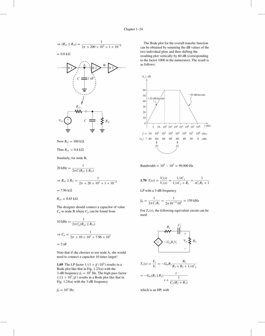
Chapter 1–24
⇒ (Ro1 ‖ Ri2) = 1
2π × 200× 103 × 1× 10−9
= 0.8 k�
Cvo1 Ri2
Ro1
��
A
1 nF
# 1 # 2 # 3B
C
Now Ri2 = 100 k�.
Thus Ro1 0.8 k�
Similarly, for node B,
20 kHz = 1
2πC(Ro2 ‖ Ri3)
⇒ Ro2 ‖ Ri3 = 1
2π × 20× 103 × 1× 10−9
= 7.96 k�
Ro2 = 8.65 k�
The designer should connect a capacitor of valueCp to node B where Cp can be found from
10 kHz = 1
2πCp(Ro2 ‖ Ri3)
⇒ Cp = 1
2π × 10× 103 × 7.96× 103
= 2 nF
Note that if she chooses to use node A, she wouldneed to connect a capacitor 10 times larger!
1.69 The LP factor 1/(1+ jf /105) results in aBode plot like that in Fig. 1.23(a) with the3-dB frequency f0 = 105 Hz. The high-pass factor1/(1+ 102/jf ) results in a Bode plot like that inFig. 1.24(a) with the 3-dB frequency
f0 = 102 Hz.
The Bode plot for the overall transfer functioncan be obtained by summing the dB values of thetwo individual plots and then shifting theresulting plot vertically by 60 dB (correspondingto the factor 1000 in the numerator). The result isas follows:
60
50
40
30
20
10
01 10 102 103 104 105 106 107 108 f (Hz)
(Hz)f = 10 102 103 104 105 106 107 108
(dB)–~ 40 60
57 57
60 60 60 40 20 0
�20 dB/decade�20 dB/decade�20 dB/decade
�Av�, dB
�Av�
Bandwidth = 105 − 102 = 99,900 Hz
1.70 Ti(s) = Vi(s)
Vs(s)= 1/sC1
1/sC1 + R1= 1
sC1R1 + 1
LP with a 3-dB frequency
f0i = 1
2πC1R1= 1
2π10−11105 = 159 kHz
For To(s), the following equivalent circuit can beused:
�
�
�GmR2ViVo R3
R2C2
To(s) = Vo
Vi= −GmR2
R3
R2 + R3 + 1/sC2
= −Gm(R2 ‖R3)s
s+ 1
C2(R2 + R3)
which is an HP, with
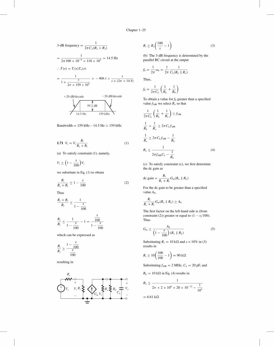
Chapter 1–25
3-dB frequency = 1
2πC2(R2 + R3)
= 1
2π100× 10−9 × 110× 103 = 14.5 Hz
∴ T (s) = Ti(s)To(s)
= 1
1+ s
2π × 159× 103
× − 909.1× s
s+ (2π × 14.5)
�20 dB/decade�20 dB/decade
14.5 Hz 159 kHz
59.2 dB
Bandwidth = 159 kHz – 14.5 Hz 159 kHz
1.71 Vi = VsRi
Rs + Ri(1)
(a) To satisfy constraint (1), namely,
Vi ≥(
1− x
100
)Vs
we substitute in Eq. (1) to obtain
Ri
Rs + Ri≥ 1− x
100(2)
Thus
Rs + Ri
Ri≤ 1
1− x
100
Rs
Ri≤ 1
1− x
100
− 1 =x
100
1− x
100
which can be expressed as
Ri
Rs≥
1− x
100x
100
resulting in
Vi VoRi Ro RLCL
Vs
Rs
Gm Vi
�
�
�
�
�
�
Ri ≥ Rs
(100
x− 1
)(3)
(b) The 3-dB frequency is determined by theparallel RC circuit at the output
f0 = 1
2πω0 = 1
2π
1
CL(RL ‖ Ro)
Thus,
f0 = 1
2πCL
(1
RL+ 1
R0
)
To obtain a value for f0 greater than a specifiedvalue f3dB we select Ro so that
1
2πCL
(1
RL+ 1
Ro
)≥ f3dB
1
RL+ 1
Ro≥ 2πCL f3dB
1
Ro≥ 2πCL f3dB − 1
RL
Ro ≤ 1
2π f3dBCL − 1
RL
(4)
(c) To satisfy constraint (c), we first determinethe dc gain as
dc gain = Ri
Rs + RiGm(Ro ‖ RL)
For the dc gain to be greater than a specifiedvalue A0,
Ri
Rs + RiGm(Ro ‖ RL) ≥ A0
The first factor on the left-hand side is (fromconstraint (2)) greater or equal to (1− x/100).Thus
Gm ≥ A0(1− x
100
)(Ro ‖ RL)
(5)
Substituting Rs = 10 k� and x = 10% in (3)results in
Ri ≥ 10
(100
100− 1
)= 90 k�
Substituting f3dB = 2 MHz, CL = 20 pF, and
RL = 10 k� in Eq. (4) results in
Ro ≤ 1
2π × 2× 106 × 20× 10−12 − 1
104
= 6.61 k�
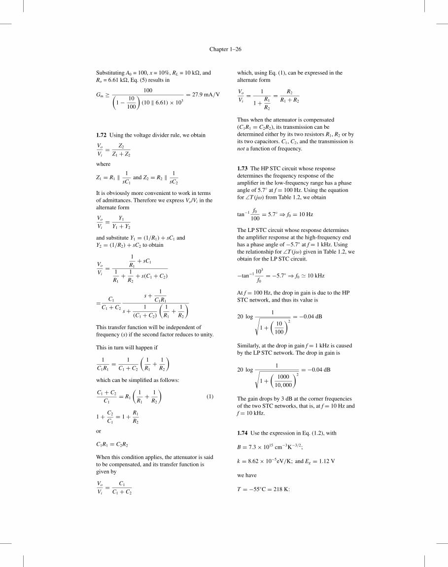
Chapter 1–26
Substituting A0 = 100, x = 10%, RL = 10 k�, andRo = 6.61 k�, Eq. (5) results in
Gm ≥ 100(1− 10
100
)(10 ‖ 6.61)× 103
= 27.9 mA/V
1.72 Using the voltage divider rule, we obtain
Vo
Vi= Z2
Z1 + Z2
where
Z1 = R1 ‖ 1
sC1and Z2 = R2 ‖ 1
sC2
It is obviously more convenient to work in termsof admittances. Therefore we express Vo/Vi in thealternate form
Vo
Vi= Y1
Y1 + Y2
and substitute Y1 = (1/R1)+ sC1 andY2 = (1/R2)+ sC2 to obtain
Vo
Vi=
1
R1+ sC1
1
R1+ 1
R2+ s(C1 + C2)
= C1
C1 + C2
s+ 1
C1R1
s+ 1
(C1 + C2)
(1
R1+ 1
R2
)
This transfer function will be independent offrequency (s) if the second factor reduces to unity.
This in turn will happen if
1
C1R1= 1
C1 + C2
(1
R1+ 1
R2
)
which can be simplified as follows:
C1 + C2
C1= R1
(1
R1+ 1
R2
)(1)
1+ C2
C1= 1+ R1
R2
or
C1R1 = C2R2
When this condition applies, the attenuator is saidto be compensated, and its transfer function isgiven by
Vo
Vi= C1
C1 + C2
which, using Eq. (1), can be expressed in thealternate form
Vo
Vi= 1
1+ R1
R2
= R2
R1 + R2
Thus when the attenuator is compensated(C1R1 = C2R2), its transmission can bedetermined either by its two resistors R1, R2 or byits two capacitors. C1, C2, and the transmission isnot a function of frequency.
1.73 The HP STC circuit whose responsedetermines the frequency response of theamplifier in the low-frequency range has a phaseangle of 5.7◦ at f = 100 Hz. Using the equationfor ∠T (jω) from Table 1.2, we obtain
tan−1 f0
100= 5.7◦ ⇒ f0 = 10 Hz
The LP STC circuit whose response determinesthe amplifier response at the high-frequency endhas a phase angle of −5.7◦ at f = 1 kHz. Usingthe relationship for ∠T (jω) given in Table 1.2, weobtain for the LP STC circuit.
−tan−1 103
f0= −5.7◦ ⇒ f0 10 kHz
At f = 100 Hz, the drop in gain is due to the HPSTC network, and thus its value is
20 log1√
1+(
10
100
)2= −0.04 dB
Similarly, at the drop in gain f = 1 kHz is causedby the LP STC network. The drop in gain is
20 log1√
1+(
1000
10, 000
)2= −0.04 dB
The gain drops by 3 dB at the corner frequenciesof the two STC networks, that is, at f = 10 Hz andf = 10 kHz.
1.74 Use the expression in Eq. (1.2), with
B = 7.3× 1015 cm−3K−3/2;
k = 8.62× 10⁻⁵eV/K; and Eg = 1.12 V
we have
T = −55◦C = 218 K:
Chapter 1–27
ni = 2.68× 106 cm−3;N
ni= 1.9× 10¹⁶
That is, one out of every 1.9× 10¹⁶ silicon atomsis ionized at this temperature.
T = 0◦C = 273 K:
ni = 1.52× 109 cm−3;N
ni= 3.3× 10¹³
T = 20◦C = 293 K:
ni = 8.60× 109 cm−3;N
ni= 5.8× 10¹²
T = 75◦C = 348 K:
ni = 3.70× 1011 cm−3;N
ni= 1.4× 10¹¹
T = 125◦C = 398 K:
ni = 4.72× 1012 cm−3;N
ni= 1.1× 10¹⁰
1.75 Use Eq. (1.2) to find ni,
ni = BT 3/2 e−Eg/2kT
Substituting the values given in the problem,
ni = 3.56× 10¹⁴(300)3/2e−1.42/(2×8.62×10−5×300)
= 2.2× 10⁶ carriers/cm3
1.76 Since NA ni, we can write
pp ≈ NA = 5× 1018 cm−3
Using Eq. (1.3), we have
np = n2i
pp= 45 cm−3
1.77 T = 27◦C = 273+ 27 = 300 K
At 300 K, ni = 1.5× 10¹⁰/cm3
Phosphorus-doped Si:
nn ND = 1017/cm3
pn = n2i
ND= (1.5× 10¹⁰)
2
1017 = 2.25× 10³/cm3
Hole concentration = pn = 2.25× 10³/cm3
T = 125◦C = 273+ 125 = 398 K
At 398 K, ni = BT 3/2e−Eg/2kT
= 7.3× 1015 × (398)3/2e−1.12/(2×8.62×10−5×398)
= 4.72× 10¹²/cm3
pn = n2i
ND= 2.23× 10⁸/cm3
At 398 K, hole concentration is
pn = 2.23× 10⁸/cm3
1.78 Hole concentration in intrinsic Si = ni
ni = BT 3/2 e−Eg/2kT
= 7.3× 10¹⁵(300)3/2e−1.12/(2×8.62×10−5×300)
= 1.5× 10¹⁰ holes/cm3
In phosphorus-doped Si, hole concentration dropsbelow the intrinsic level by a factor of 108.
∴ Hole concentration in P-doped Si is
pn = 1.5× 10¹⁰
108 = 1.5× 102 cm−3
Now, nn ND and pnnn = n2i
nn = n2i /pn = (1.5× 10¹⁰)
2
1.5× 102
= 1.5× 1018 cm−3
ND = nn = 1.5× 10¹⁸ atoms/cm3
1.79 (a) The resistivity of silicon is given byEq. (1.41):
For intrinsic silicon,
p = n = ni = 1.5× 1010 cm−3
Using μn = 1350 cm2/V · s and
μp = 480 cm2/V · s, and q = 1.6× 10⁻¹⁹ C wehave
ρ = 2.28× 10⁵ �-cm.
Using R = ρ · L
Awith L = 0.001 cm and
A = 3× 10⁻⁸ cm2, we have
R = 7.6× 10⁹ �.
Chapter 1–28
(b) nn ≈ ND = 5× 1016 cm−3;
pn = n2i
nn= 4.5× 103 cm−3
Using μn = 1200 cm2/V · s and
μp = 400 cm2/V · s, we have
ρ = 0.10 �-cm; R = 3.33 k�.
(c) nn ≈ ND = 5× 1018 cm−3;
pn = n2i
nn= 45 cm−3
Using μn = 1200 cm2/V · s andμp = 400 cm2/V · s, we have
ρ = 1.0× 10⁻³ �-cm; R = 33.3 �.
As expected, since ND is increased by 100, theresistivity decreases by the same factor.
(d) pp ≈ NA = 5× 1016 cm−3; np = n2i
nn
= 4.5× 103 cm−3
ρ = 0.31 �-cm; R = 10.42 k�
(e) Since ρ is given to be 2.8× 10⁻⁶ �-cm, wedirectly calculate R = 9.33× 10⁻² �.
1.80 Cross-sectional area of Si bar
= 5× 4 = 20 μm2
Since 1 μm = 10−4 cm, we get
= 20× 10−8 cm2
Current I = Aq(pμp + nμn)E
= 20× 10−8 × 1.6× 10−19
(1016 × 500+ 104 × 1200)× 1 V
10× 10−4
= 160 μA
1.81 Electric field:
E = 3 V
10 μm= 3 V
10× 10−6 m
= 3 V
10× 10−4 cm
= 3000 V/cm
�3 V�
10 μm
νp-drift = μpE = 480× 3000
= 1.44× 106 cm/s
νn-drift = μnE = 1350× 3000
= 4.05× 106 cm/s
νn
νp= 4.05× 10⁶
1.44× 106 = 2.8125 or
νn = 2.8125 νp
Or, alternatively, it can be shown as
νn
νp= μnE
μpE= μn
μp= 1350
480
= 2.8125
1.82
pn0 = n2i
ND= (1.5× 10¹⁰)
2
1016 = 2.25× 10⁴/cm3
From Fig. P1.82,
dp
dx= −108pn0 − pn0
W − 108pn0
50× 10−7
since 1 nm = 10−7 cm
dp
dx= −108 × 2.25× 104
50× 10−7
= −4.5× 10¹⁷
Hence
Jp = −qDpdp
dx
= −1.6× 10−19 × 12× (−4.5× 10¹⁷)
= 0.864 A/cm2
1.83 Use Eq. (1.45):Dn
μn
= Dp
μp
= VT
Dn = μnVT and Dp = μpVT whereVT = 25.9 mV.
Chapter 1–29
DopingConcentration μn μp Dn Dp
(carriers/cm3) cm2/V · s cm2/V · s cm2/s cm2/s
Intrinsic 1350 480 35 12.4
1016 1200 400 31 10.4
1017 750 260 19.4 6.7
1018 380 160 9.8 4.1
1.84 Using Eq. (1.46) and NA = ND
= 5× 1016 cm−3 and ni = 1.5× 1010 cm−3,
we have V0 = 778 mV.
Using Eq. (1.50) andεs = 11.7× 8.854× 10−14 F/cm, we haveW = 2× 10⁻⁵ cm = 0.2 μm. The extension ofthe depletion width into the n and p regions isgiven in Eqs. (1.51) and (1.52), respectively:
xn = W · NA
NA + ND= 0.1 μm
xp = W · ND
NA + ND= 0.1 μm
Since both regions are doped equally, thedepletion region is symmetric.
Using Eq. (1.53) andA = 20 μm2 = 20× 10−8 cm2, the chargemagnitude on each side of the junction is
QJ = 1.6× 10⁻¹⁴ C.
1.85 From Table 1.3,
VT at 300 K = 25.9 mV
Using Eq. (1.46), built-in voltage V0 is obtained:
V0 = VT ln
(NAND
n2i
)= 25.9× 10⁻³×
ln
(1017 × 1016(1.5× 10¹⁰
)2
)
= 0.754 V
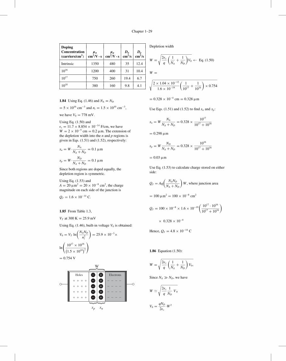
� �
� �
� �
� �
� �
� � � � � � � �
� � � � � � � �
� � � � � � � �
� � � � � � � �
xp xn
W
Holes Electrons
Depletion width
W =√
2εs
q
(1
NA+ 1
ND
)V0 ← Eq. (1.50)
W =√
2× 1.04× 10−12
1.6× 10⁻¹⁹
(1
1017 +1
1016
)× 0.754
= 0.328× 10⁻⁴ cm = 0.328 μm
Use Eqs. (1.51) and (1.52) to find xn and xp:
xn = WNA
NA + ND= 0.328× 10¹⁷
1017 + 1016
= 0.298 μm
xp = WND
NA + ND= 0.328× 10¹⁶
1017 + 1016
= 0.03 μm
Use Eq. (1.53) to calculate charge stored on eitherside:
QJ = Aq
(NAND
NA + ND
)W , where junction area
= 100 μm2 = 100× 10−8 cm2
QJ = 100× 10−8 × 1.6× 10−19
(1017 · 1016
1017 + 1016
)
× 0.328× 10⁻⁴
Hence, QJ = 4.8× 10⁻¹⁴ C
1.86 Equation (1.50):
W =√
2εs
q
(1
NA+ 1
ND
)V0,
Since NA ND, we have
W √
2εs
q
1
NDV 0
V0 = qND
2εs·W 2
Chapter 1–30
Here W = 0.2 μm = 0.2× 10⁻⁴ cm
So V0 = 1.6× 10−19 × 1016 × (0.2× 10−4
)2
2× 1.04× 10−12
= 0.31 V
QJ = Aq
(NAND
NA + ND
)W ∼= AqNDW
since NA ND, we have QJ = 3.2 fC.
1.87 V0 = VT ln
(NAND
n2i
)
If NA or ND is increased by a factor of 10, thennew value of V0 will be
V0 = VT ln
(10 N AND
n2i
)
The change in the value of V0 isVT ln10 = 59.6 mV.
1.88 Using Eq. (1.46) with NA = 1017 cm−3,ND = 1016 cm−3, and ni = 1.5× 10¹⁰, we haveV0 = 754 mV
Using Eq. (1.55) with VR = 5 V, we haveW = 0.907 μm.
Using Eq. (1.56) with A = 1× 10⁻⁶ cm2, wehave QJ = 13.2× 10⁻¹⁴ C.
1.89 Equation (1.55):
W =√
2εs
q
(1
NA+ 1
ND
)(V0 + VR)
=√
2εs
q
(1
NA+ 1
ND
)V0
(1+ VR
V0
)
= W0
√1+ VR
V0
Equation (1.56):
Qj = A
√2εsq
(NA N D
NA + ND
)· (V0 + VR)
= A
√2εsq
(NA N D
NA + ND
)V0 ·
(1+ VR
V0
)
= QJ 0
√1+ VR
V0
1.90 Equation (1.63):
I = Aqn2i
(Dp
LpND+ Dn
LnNA
) (eV /VT − 1
)
Here Ip = Aqn2i
Dp
LpND
(eV /VT − 1
)
In = Aqn2i
Dn
LnNA
(eV /VT − 1
)Ip
In= Dp
Dn· Ln
Lp·NA
ND
= 10
20× 10
5× 10¹⁸
1016
Ip
In= 100
Now I = Ip + In = 100 I n + In ≡ 1 mA
In = 1
101mA = 0.0099 mA
Ip = 1− In = 0.9901 mA
1.91 Equation (1.65):
IS = Aqn2i
(Dp
LpND+ Dn
LnNA
)
A = 100 μm2 = 100× 10−8 cm2
IS = 100× 10−8 × 1.6× 10−19 × (1.5× 1010)2
(10
5× 10−4 × 1016 +18
10× 10−4 × 1017
)
= 7.85× 10⁻¹⁷ A
I ∼= ISeV /VT
= 7.85× 10⁻¹⁷ × e750/25.9
∼= 0.3 mA
1.92 ni = BT 3/2e−Eg/2kT
At 300 K,
ni = 7.3× 1015 × (300)3/2×e−1.12/(2×8.62×10−5×300)
= 1.4939× 10¹⁰/cm2
n2i (at 300 K) = 2.232× 10²⁰
Chapter 1–31
At 305 K,
ni = 7.3× 1015 × (305)3/2× e−1.12/(2×8.62×10−5×305)
= 2.152× 10¹⁰
n2i (at 305 K) = 4.631× 10²⁰
son2
i (at 305 K)
n2i (at 300 K)
= 2.152
Thus IS approximately doubles for every 5◦C risein temperature.
1.93 Equation (1.63):
I = Aqn2i
(Dp
LpND+ Dn
LnNA
) (eV /VT − 1
)
So Ip = Aqn2i
Dp
LpND
(eV /VT − 1
)
In = Aqn2i
Dn
LnNA
(eV /VT − 1
)For p+−n junction NA ND, thus Ip In and
I Ip = Aqn2i
Dp
LpND
(eV /VT − 1
)For this case using Eq. (1.65):
IS Aqn2i
Dp
LpND= 104 × 10−8 × 1.6× 10−19
×(1.5× 1010)2 10
10× 10−4 × 1017
= 3.6× 10⁻¹⁶ A
I = IS
(eV /VT − 1
) = 1.0× 10⁻³
3.6× 10⁻¹⁶(
eV /(25.9×10−3) − 1)= 1.0× 10⁻³
⇒ V = 0.742 V
1.94 Equation (1.72):
Cj0 = A
√( εsq
2
)( NAND
NA + ND
)(1
V0
)
V0 = VT ln
(NAND
n2i
)
= 25.9× 10⁻³ × ln
(1017 × 1016(1.5× 10¹⁰
)2
)
= 0.754 V
Cj0 = 100× 10−8
√√√√(1.04× 10−12 × 1.6× 10−19
2
)(1017 × 1016
1017 + 1016
)1
0.754
= 31.6 fF
Cj = Cj0√1+ VR
V0
= 31.6 fF√1+ 3
0.754
= 14.16 fF
1.95 Equation (1.73), Cj = Cj0(1+ VR
V0
)m
For VR = 1 V, Cj = 0.4 pF(1+ 1
0.75
)1/3
= 0.3 pF
For VR = 10 V, Cj = 0.4 pF(1+ 10
0.75
)1/3
= 0.16 pF
1.96 Equation (1.67):
α = A
√2εsq
NAND
NA + ND
Equation (1.69):
Cj = α
2√
V0 + VR
Substitute for α from Eq. (1.67):
Cj =A
√2εsq
NAND
NA + ND
2√
V0 + VR
×√
εs√εs
= Aεs × 1√2εs
q
(NA + ND
NAND
)(V0 + VR)
= εsA1√
2εs
q
(1
NA+ 1
ND
)(V0 + VR)
= εsA
W
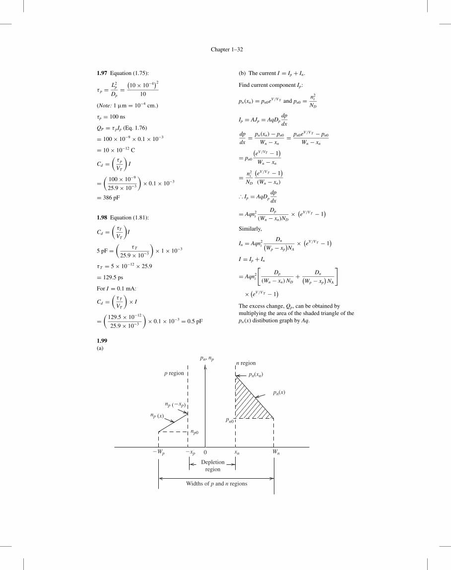
Chapter 1–32
1.97 Equation (1.75):
τ p =L2
p
Dp=(10× 10−4
)2
10
(Note: 1 μm = 10−4 cm.)
τp = 100 ns
QP = τ pIp (Eq. 1.76)
= 100× 10−9 × 0.1× 10−3
= 10× 10−12 C
Cd =(
τ p
VT
)I
=(
100× 10−9
25.9× 10⁻³
)× 0.1× 10−3
= 386 pF
1.98 Equation (1.81):
Cd =(
τT
VT
)I
5 pF =(
τ T
25.9× 10⁻³
)× 1× 10⁻³
τ T = 5× 10−12 × 25.9
= 129.5 ps
For I = 0.1 mA:
Cd =(
τ T
VT
)× I
=(
129.5× 10⁻¹²
25.9× 10⁻³
)× 0.1× 10−3 = 0.5 pF
1.99(a)
Widths of p and n regions
Depletionregion
xn�xp 0�Wp
np (x)pn0
np0
n region
p region
pn, np
pn(xn)
pn(x)
np (�xp)
Wn
(b) The current I = Ip + In.
Find current component Ip:
pn(xn) = pn0eV /V T and pn0 = n2i
ND
Ip = AJp = AqDpdp
dx
dp
dx= pn(xn)− pn0
Wn − xn= pn0eV /V T − pn0
Wn − xn
= pn0
(eV /VT − 1
)Wn − xn
= n2i
ND
(eV /V T − 1
)(Wn − xn)
∴ Ip = AqDp
dp
dx
= Aqn2i
Dp
(Wn − xn)ND× (
eV /V T − 1)
Similarly,
In = Aqn2i
Dn(Wp − xp
)NA× (
eV /V T − 1)
I = Ip + In
= Aqn2i
[Dp
(Wn − xn) ND+ Dn(
Wp − xp
)NA
]
× (eV /V T − 1)
The excess change, Qp, can be obtained bymultiplying the area of the shaded triangle of thepn(x) distibution graph by Aq.
Chapter 1–33
Qp = Aq× 1
2[pn (xn)− pn0] (Wn − xn)
= 1
2Aq[pn0eV /V T − pn0
](Wn − xn)
= 1
2Aqpn0
(eV /V T − 1
)(Wn − xn)
= 1
2Aq
ni2
ND(Wn − xn)
(eV /V T − 1
)
= 1
2
(Wn − xn)2
Dp· Ip
1
2
W 2n
DP· Ip for Wn xn
(c) For Q Qp, I Ip,
Q 1
2
W 2n
DpI
Thus, τT = 1
2
W 2n
Dp, and
Cd = dQ
dV= τ T
dI
dV
But I = IS
(eV /V T − 1
)dI
dV= ISeV /V T
VT I
VT
so Cd∼= τ T · I
VT.
(d) Cd = 1
2
W 2n
10
1× 10⁻³
25.9× 10−3 = 8× 10⁻¹² F
Solve for Wn:
Wn = 0.64 μm