Embed Size (px)
Citation preview

Lappeenranta–Lahti University of Technology LUTSchool of Energy SystemsDegree Programme in Electrical Engineering
Matti Salervo
INSTRUMENTATION ELECTRONICSFOR A NOVEL OPTICAL GAS SENSOR
Master’s Thesis
Examiners: Prof. Pertti SilventoinenM.Sc. (Tech.) Markus Huuhtanen

ABSTRACT
Lappeenranta–Lahti University of Technology LUTSchool of Energy SystemsDegree Programme in Electrical Engineering
Matti Salervo
INSTRUMENTATION ELECTRONICSFOR A NOVEL OPTICAL GAS SENSOR
Master’s Thesis
2020
88 pages, 40 figures, 5 tables, 1 appendix.
Examiners: Prof. Pertti SilventoinenM.Sc. (Tech.) Markus Huuhtanen
Keywords: analog electronics, analog signal processing, electronics design,infrared spectroscopy, optical gas sensing, photodetector, printed circuit board design
Optical gas sensors are measuring instruments that can be used to determine the concen-tration of various gases, such as carbon dioxide. They are widely utilized in many areas ofindustry. In this master’s thesis commissioned by Vaisala Oyj, instrumentation electronicsand a printed circuit board were designed for a novel optical nondispersive infrared gassensor prototype. Previously designed separate test circuits were used as a basis for thedesign work done. The research objective of the thesis was approached by utilizing theapplicable parts of the design science research method. A functioning single-circuit-boardprototype device was achieved as the main result of the work done. The main features ofthe prototype were experimentally tested. In the end, after small modifications made, theprototype’s subassemblies operated as planned. Further research is needed especially tooptimize the electronics and the printed circuit board design, as well as to define the ac-tual performance of the prototype by using it to measure known target gas concentrations.
TIIVISTELMÄ
Lappeenrannan–Lahden teknillinen yliopisto LUTSchool of Energy SystemsSähkötekniikan koulutusohjelma
Matti Salervo
INSTRUMENTOINTIELEKTRONIIKAN TOTEUTUSUUDENLAISTA OPTISTA KAASUANTURIA VARTEN
Diplomityö
2020
88 sivua, 40 kuvaa, 5 taulukkoa, 1 liite.
Työn tarkastajat: Prof. Pertti SilventoinenDI Markus Huuhtanen
Hakusanat: analogiaelektroniikka, analogiasignaalin käsittely, elektroniikkasuunnittelu,fotodetektori, infrapunaspektroskopia, optiset kaasumittaukset, piirilevysuunnittelu
Optiset kaasuanturit ovat mittausinstrumentteja, joita voidaan käyttää monien eri kaa-sujen, kuten hiilidioksidin, konsentraation määrittämiseen. Niitä hyödynnetään laajamit-taisesti useilla teollisuuden aloilla. Tässä Vaisala Oyj:n toimeksiannosta tehdyssä diplo-mityössä suunniteltiin instrumentointielektroniikka sekä piirilevy uudenlaisen optisen ei-dispersiivisen infrapunakaasuanturin prototyyppiä varten. Tehdyn suunnittelutyön pohja-na käytettiin aikaisemmin suunniteltuja toisistaan erillisiä testipiirejä. Tutkimuksen ta-voitetta lähestyttiin hyödyntämällä suunnittelutieteellistä tutkimusmenetelmää sen sovel-tuvilta osin. Työn tärkein tulos on osana sitä toteutettu toiminnallinen yhden piirilevynprototyyppilaite. Prototyypin pääominaisuuksia testattiin kokeellisesti. Pienten muutostenjälkeen prototyypin osakokonaisuuksien todettiin toimivan suunnitellusti. Jatkotutkimus-ta tarvitaan erityisesti suunnitellun elektroniikan ja piirilevyn optimoimiseksi, sekä proto-tyypin suorituskyvyn määrittämiseksi tunnettuja kohdekaasun pitoisuuksia mittaamalla.

PREFACE
I would first like to thank the examiners of this thesis, as well as all of my colleagues,for their invaluable contribution to this work. Thank you professor Silventoinen forall the tips and feedback regarding general arrangements and academic writing. Thankyou Markus H. and Asko N. for assisting me with the electronics design, Marko H.for the embedded software and Esa K. for the mechanics. I would also like to collec-tively thank my superiors and the whole of Vaisala Oyj for providing me this wonderfulopportunity. This company is filled with truly amazing people; kind souls that are ab-solute top talents of their versatile areas of expertise. It has been a genuine pleasureto begin my career by being a part of this laid-back yet highly professional community.
To my family; thank you for unconditionally supporting me throughout all these years,even during the most difficult and uncertain times. The encouragement I have receivedfrom you means the world to me. To Sakari, Krister, Ossi, J-P and all of my otherdear friends & fellow students from the LUT department of Electrical Engineering; Iwould never have made it academically this far without you – thank you for everything.
I would like to dedicate this work to my fiancée Karoliina and my son Väinö – thereare no words to express my gratitude for all the understanding, support, love and joy thatboth of you have given to me throughout the process of writing this thesis and all the yearsI have been blessed to spend with you.
Vantaanlaakso, July 18, 2020
Matti Salervo

5
CONTENTS
1 INTRODUCTION 81.1 Background & motivation . . . . . . . . . . . . . . . . . . . . . . . . . 91.2 Objectives & delimitations . . . . . . . . . . . . . . . . . . . . . . . . . 101.3 Research methods & materials . . . . . . . . . . . . . . . . . . . . . . . 111.4 Structure of the thesis . . . . . . . . . . . . . . . . . . . . . . . . . . . . 11
2 ABSORPTION SPECTROSCOPY 122.1 Electromagnetic spectrum & absorption of radiation . . . . . . . . . . . . 122.2 Infrared absorption spectroscopy . . . . . . . . . . . . . . . . . . . . . . 152.3 Infrared radiation emitters . . . . . . . . . . . . . . . . . . . . . . . . . 17
2.3.1 Electroluminescent sources . . . . . . . . . . . . . . . . . . . . . 182.3.2 Incandescent sources . . . . . . . . . . . . . . . . . . . . . . . . 19
2.4 Optical filters . . . . . . . . . . . . . . . . . . . . . . . . . . . . . . . . 212.5 Infrared detectors . . . . . . . . . . . . . . . . . . . . . . . . . . . . . . 23
2.5.1 Thermal detectors . . . . . . . . . . . . . . . . . . . . . . . . . . 232.5.2 Photonic detectors . . . . . . . . . . . . . . . . . . . . . . . . . 25
3 ELECTRONICS THEORY 283.1 Operational amplifiers . . . . . . . . . . . . . . . . . . . . . . . . . . . 283.2 Analog-to-digital converters . . . . . . . . . . . . . . . . . . . . . . . . 313.3 DC voltage regulators . . . . . . . . . . . . . . . . . . . . . . . . . . . . 323.4 Infrared signal modulation . . . . . . . . . . . . . . . . . . . . . . . . . 333.5 Thermoelectric cooling . . . . . . . . . . . . . . . . . . . . . . . . . . . 343.6 Digital control . . . . . . . . . . . . . . . . . . . . . . . . . . . . . . . . 36
4 ELECTRONICS DESIGN 384.1 Passive components . . . . . . . . . . . . . . . . . . . . . . . . . . . . . 404.2 Control of infrared source & tunable optical filter . . . . . . . . . . . . . 404.3 Infrared photodetectors . . . . . . . . . . . . . . . . . . . . . . . . . . . 41
4.3.1 Detector type 1: VIGO System PVIA-2TE-λopt . . . . . . . . . . 424.3.2 Detector type 2: Hamamatsu Photonics P13243 . . . . . . . . . . 43
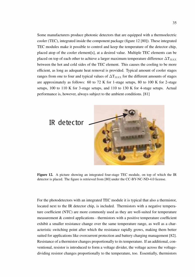
4.4 Photodetector signal amplification . . . . . . . . . . . . . . . . . . . . . 454.4.1 Stage 1: transimpedance amplifier . . . . . . . . . . . . . . . . . 454.4.2 Stage 2: inverting amplifier . . . . . . . . . . . . . . . . . . . . . 474.4.3 Design verification by simulation . . . . . . . . . . . . . . . . . 48
4.5 Detector temperature control . . . . . . . . . . . . . . . . . . . . . . . . 494.5.1 General setup . . . . . . . . . . . . . . . . . . . . . . . . . . . . 50

6
4.5.2 Thermistor linearization . . . . . . . . . . . . . . . . . . . . . . 524.5.3 Control signal filter . . . . . . . . . . . . . . . . . . . . . . . . . 554.5.4 Heat dissipation . . . . . . . . . . . . . . . . . . . . . . . . . . . 56
4.6 Microcontroller unit . . . . . . . . . . . . . . . . . . . . . . . . . . . . . 584.7 Supply & operating voltages . . . . . . . . . . . . . . . . . . . . . . . . 59
5 PRINTED CIRCUIT BOARD DESIGN 625.1 General requirements & design rules . . . . . . . . . . . . . . . . . . . . 625.2 Layer setup & interconnections . . . . . . . . . . . . . . . . . . . . . . . 635.3 Component layout & routing . . . . . . . . . . . . . . . . . . . . . . . . 645.4 Automated error checking . . . . . . . . . . . . . . . . . . . . . . . . . 66
6 EVALUATING OPERATION OF THE PROTOTYPE 676.1 Description of experiments . . . . . . . . . . . . . . . . . . . . . . . . . 676.2 Measurement setups . . . . . . . . . . . . . . . . . . . . . . . . . . . . . 686.3 Results & discussion . . . . . . . . . . . . . . . . . . . . . . . . . . . . 696.4 Future work . . . . . . . . . . . . . . . . . . . . . . . . . . . . . . . . . 76
7 CONCLUSION 78
REFERENCES 79
APPENDICESAppendix 1: MCU Pin Configuration

7
LIST OF SYMBOLS & ABBREVIATIONSA Absorbance, Amplification, AreaC Concentration [M]D* Specific Detectivity [cmHz1/2W−1, Jones]
I Radiation Intensity [W
cm2]
k Absorption Coefficient [M · cm−1]L Optical Path Length [cm]NEP Noise Equivalent Power [W/
√Hz]
S Photosensitivity [A/W, V/W]
λ, λp Wavelength, Peak Sensitivity Wavelength [µm]µG Microglow; a Vaisala-Patented Silicon MEMS Emitter Infrared SourceΣΔ Sigma–Delta, a Subcategory of Analog-to-Digital Convertersτ Response Time, Time Constant [ms, ns]
A/D Analog-to-DigitalADC Analog-to-Digital ConverterASIC Application-Specific Integrated CircuitEM ElectromagneticFIR Far Infrared (15-1000 µm)FPI Fabry–Pérot InterferometerIR InfraredLED Light-emitting DiodeLWIR Long-Wavelength Infrared (8-15 µm)MCU Microcontroller UnitMEMS Microelectromechanical SystemMWIR Mid-Wavelength Infrared (3-8 µm)NDIR Nondispersive InfraredNIR Near Infrared (0.75-1.40 µm)NTC Negative Temperature CoefficientOP-AMP Operational AmplifierPCB Printed Circuit BoardPID Proportional—Integral—DerivativePWM Pulse-Width ModulationSNR Signal-to-Noise RatioSWIR Short-Wavelength Infrared (1.40-3.00 µm)TEC Thermoelectric CoolerTIA Transimpedance AmplifierTO Transistor Outline; a Component Package Type

8
1 INTRODUCTION
Interestingly, the practice of using canary birds for detecting hazardous gases inside coalmines had not been completely stopped in the United Kingdom until as recently as just afew decades ago [1]. As seen in figure 1 [2], not only birds but also other small animalslike rabbits have been historically used for similar kinds of purposes. This is becausesmaller animals typically react to considerably lower concentrations of many lethal gasesthan humans do [3], thus offering their possessor an opportunity to escape from the dangerzone or take other measures required to normalize the situation.
Figure 1. A 1970’s public domain photograph by a Denver Post photographer, showing a cagedrabbit being used to monitor for potential sarin gas leaks at a chemical plant manufacturing thenotorious nerve agent. The figure is retrieved from [2].
Fortunately for the canaries and other sentinel species alike, scientists and engineers haveinvented more accurate and reliable methods for detecting and monitoring the concentra-tion of many types of gases [4]. One of these modern methods, or branches of technol-ogy, is optical gas sensing. It should be noted that the aforementioned mining industrycertainly is not the only utilizer of this technology. Instead, many kinds of optical gas

9
sensors are used for a wide variety of applications in different fields of industry, such asbuilding automation, life sciences, process safety and food industry. Optical gas sensorscan be sorted into subcategories based on their operating principle. This thesis focuseson nondispersive infrared sensing, which is an absorption-based optical gas sensing tech-nology - however, it is notable that also non-absorption-based gas sensing technologiesexist and are well suited for some applications, like low-concentration ambient air qualitymeasurements [5].
Due to their highly application-specific nature, it would be difficult to make substantiatedclaims that there would be distinguishable technology-wide historical turning points inthe development of optical gas sensors. Not any single method has been able to stand outand gain a significant market share in the industry [6], instead the perception created bythe different commercial actors in the field - as well as actual customer need for certainfeatures - has dominantly guided the development work towards multiple directions thathave changed over time due to changes in the industry. In practice this could mean, forexample, pursuing for miniaturization of a device or the objective of trying to achievea higher accuracy or a wider measuring range [6]. Pursuit of improved performance ofan existing technology is essentially the goal of this thesis too, as described later in thischapter.
1.1 Background & motivation
At Vaisala Oyj (hereinafter referred to as Vaisala) both new applications for existing mea-surement technologies and new measurement technologies for existing and potentiallyprofitable applications are constantly being studied and developed. The company investssignificantly in research and development; at the time of writing up to 13% of the com-pany’s net sales is invested in R&D and about 22% of the ca. 1,800 Vaisala employeesworldwide work within R&D activities [7,8]. At the Vaisala Industrial Measurements de-partment, versatile development work related to the CARBOCAP® optical nondispersiveinfrared gas sensing technology has been done over the years. One of the many aspectsof the development work is to shorten the response time as well as to further improvemeasurement sensitivity. This type of rapid yet highly responsive optical gas measure-ment technology has several interesting potential applications related to both industrialand environmental measurements, including but not limited to the uninterruptedly mov-ing production lines of food and beverage industries, and monitoring fluxes of certaingases related to background air quality and agriculture [5, 9]. This thesis acts as a steptowards the commercialization of the rapid CARBOCAP® technology.

10
1.2 Objectives & delimitations
The research objective of this master’s thesis is to design and implement electronics for aprototype measuring instrument used for optical gas measurements. Most subsystems ofthe concept have been proven to work but tests with known gas concentrations have notbeen done yet. Thus, the previously created separate prototypes of the different subsys-tems will be combined to form a stand-alone single-circuit-board solution. This allowsperformance evaluation of the concept through measurements of known target gas con-centrations. As a new feature, control electronics required for the temperature control ofthe detectors used will be added onboard to complement the trial designs implemented sofar - in the past, a separate bench top device (Thorlabs TED200C) has been used for thispurpose. The prototype consists of a custom-made optical cuvette, and a printed circuitboard (PCB) containing the following electrical subsystems:
• A Vaisala Microglow (µG) IR source & a voltage-tunable optical Fabry–Pérot in-terferometer (FPI) filter and the control electronics required to operate them.
• A photodiode-based infrared (IR) detector - two alternatives are tested.
• Amplification of the measurement signal produced by the detector.
• Control & driver electronics for thermoelectric cooler (TEC) modules integratedinside both of the detectors used.
• A multi-purpose microcontroller unit (MCU) for the analog-to-digital (A/D) con-version & conditioning of the measurement signal and for controlling the prototype.
• RS-232 serial bus that enables flashing & commanding the MCU, as well as loggingmeasurement data using a command-line interface on a personal computer.
• Power management, including the main supply voltage inputs and regulating theinitial input voltage to the smaller voltage levels, as well as boosting the initialinput voltage to the higher voltage levels required.
• Passive electromagnetic interference protection & filtering.
This thesis does not consider the optomechanical design (including the mechanical de-sign of the optical cuvette, type[s] of the mirror[s] used, component alignment, focusing,et cetera) of the prototype. In addition, embedded software development necessary foroperating the prototype will be fully excluded from the scope of this work due to the lim-ited schedule. Any work related to these topics is to be completely taken care of by otherengineers of the Vaisala Industrial Measurements unit.

11
1.3 Research methods & materials
The research objective is approached by making use of the seven guidelines of the designscience research method, proposed by Havner et al. in [10], to the extent applicable.This outcome-based research method should be well-suited for the purpose of this thesisconsidering that the objective of the thesis is to produce a novel artifact (a prototypedevice) that is designed to improve the performance of existing technology, in the samemanner as Havner et al. describe the method [10].
Literary information related to the basic theory background of the field of research of thisthesis is acquired from various fundamental literary works, such as books released byacademic publishers, scientific journal articles, conference proceedings as well as thesispublications. Reference is also made to various articles and other material that is avail-able online. In addition to the academic publications and online materials, applicationnotes released by electronics manufacturers and datasheets of the electronic componentschosen are used as a reference for the design work done. The design work is partly basedon proprietary Vaisala prototype designs and experiential knowledge of the company’selectronics engineers. At the request of the company, efforts were made to use previouslyutilized components as well as suppliers to the extent possible.
1.4 Structure of the thesis
This thesis is divided into seven main chapters. First, in Chapter 1, the topic of the work isdescribed at a general level and the background, objectives and delimitation of the thesisare introduced. Then, in Chapter 2, the fundamental theory of absorption spectroscopyis explained and some components typically used and their operating principles are pre-sented. The 3rd Chapter examines the theory of electronics relevant to the design workdone, as well as the electrical properties related to the essential components used. Afterthat, Chapters 4 and 5 describe the prototype instrumentation electronics and the PCB de-signed, respectively. In Chapter 6, the measurements performed using the prototype andthe results obtained are described and discussed. Furthermore, the results are evaluatedand proposals for future work are revealed. Finally, Chapter 7 concludes the work.

12
2 ABSORPTION SPECTROSCOPY
This chapter introduces the theory background related to absorption spectroscopy, begin-ning from describing the essential concepts and ending to an introduction and comparisonof selected electronic and optical components suitable to be used in optical gas measure-ments. It should first be noted that there are many other gas sensing technologies in addi-tion to optical gas sensing. These include various methods based on observing changes inthe electrical properties of the material used for detection, like the electrochemical cells,and many other less common methods, like calorimetric and acoustic gas detectors [11].This thesis focuses on spectroscopy, which is a field of research and technology that uti-lizes the study of how electromagnetic (EM) radiation interacts with matter [12]. Morespecifically, as described by Kumar [13], absorption spectroscopy is one of the three mainbranches of spectroscopy and deals with how electromagnetic radiation is absorbed atdifferent wavelengths - the remaining two branches, scattering spectroscopy and emis-sion spectroscopy, are not relevant to this thesis and are thus ignored. The concept ofabsorption spectroscopy also includes the versatile variety of methods used to performabsorption-spectrometric measurements.
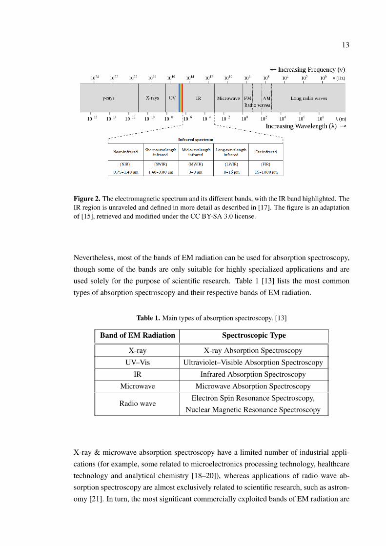
2.1 Electromagnetic spectrum & absorption of radiation
EM radiation is a form of energy that behaves both like particles and waves do [14].EM radiation is divided into different regions, called bands, that correspond to all thedifferent wavelengths and frequencies of it. These bands together form the spectrumof electromagnetic radiation, seen in figure 2 [15]. The bands of EM spectrum includegamma radiation (γ-rays), X-radiation (X-rays), ultraviolet (UV), the visible spectrum,infrared (IR), microwaves and radio waves. As the Planck–Einstein relation suggests, theshorter the wavelength of EM radiation, the higher its frequency and energy [16]. Partlybecause of this relation, very low or very high energy EM radiation cannot be widelyutilized in absorption spectroscopy; low-energy radiation may not be sufficient to changethe energy state of the observed substance, and too high an energy could lead to ionizationof the substance.
13
Figure 2. The electromagnetic spectrum and its different bands, with the IR band highlighted. TheIR region is unraveled and defined in more detail as described in [17]. The figure is an adaptationof [15], retrieved and modified under the CC BY-SA 3.0 license.
Nevertheless, most of the bands of EM radiation can be used for absorption spectroscopy,though some of the bands are only suitable for highly specialized applications and areused solely for the purpose of scientific research. Table 1 [13] lists the most commontypes of absorption spectroscopy and their respective bands of EM radiation.
Table 1. Main types of absorption spectroscopy. [13]
Band of EM Radiation Spectroscopic Type
X-ray X-ray Absorption Spectroscopy
UV–Vis Ultraviolet–Visible Absorption Spectroscopy
IR Infrared Absorption Spectroscopy
Microwave Microwave Absorption Spectroscopy
Radio waveElectron Spin Resonance Spectroscopy,
Nuclear Magnetic Resonance Spectroscopy
X-ray & microwave absorption spectroscopy have a limited number of industrial appli-cations (for example, some related to microelectronics processing technology, healthcaretechnology and analytical chemistry [18–20]), whereas applications of radio wave ab-sorption spectroscopy are almost exclusively related to scientific research, such as astron-omy [21]. In turn, the most significant commercially exploited bands of EM radiation are

14
UV/Visible and IR. Some examples of the users/uses of UV–Vis absorption spectroscopywould be the cosmetic industry, food & agriculture industry, and qualitative & quanti-tative analysis performed in the pharmaceutical industry. It should be noted that not asmany gases absorb energy on the UV–Vis band as on the IR band. A few examples ofIR absorption spectroscopy would be a variety of measurements performed for dynamicquantities, long-term monitoring of gaseous substances, as well as industrial automation& process control. Some commonly measured gases absorbing at the IR band include car-bon monoxide (CO), carbon dioxide (CO2), sulfur dioxide (SO2), nitrogen oxides (NOx),nitrous oxide (N2O, ammonia (NH3), hydrogen chloride (HCl), hydrogen fluoride (HF),methane (CH4), et cetera [22].
When EM radiation passes through a gaseous medium, may it consist of either atomsor molecules, most of the radiation passes through losslessly. Nonetheless, at somesubstance-specific wavelengths, the intensity of the incident radiation decreases, as en-ergy is absorbed into the chemical substance the medium consists of. When energy isabsorbed, the atoms or molecules contained in the medium move from their baseline en-ergy state to a more energetic, excited state. The type of transition of the energy state (e.g.electronic transition or molecular vibration/rotation) depends on the energy of the photonsin the EM radiation, which in turn is related to the wavelength of the radiation. Figure3 [23] shows the IR absorption bands of a few gases. Worth noting is that some substancesabsorb at overlapping wavelengths, which can cause measurement interference. [13]
Figure 3. IR absorption spectra of certain gases used in industrial applications. Some typicalapplications are named and their respective wavelength ranges highlighted using double-headedarrows. The figure is retrieved from [23] under the CC BY 4.0 license.

15
Especially water (H2O) absorbs IR radiation over a very wide wavelength range and over-laps with the absorption bands of many other substances. Whenever overlapping ab-sorption wavelengths are used for measuring, the need for compensation is created [22].Compensation can be carried out for example by introducing a reference measurement tothe system. Unfortunately, this would make the system more complex and increase thesources of measurement uncertainty, so whenever possible, a non-overlapping wavelengthshould be chosen to reduce the risk of cross-sensitivity.
As highlighted throughout this section, many chemical substances having some use inindustrial applications absorb on the IR band. This makes IR absorption spectroscopy anattractive subject for commercial research and development.
2.2 Infrared absorption spectroscopy
IR absorption spectroscopy can roughly cover the portion of the EM spectrum that sets inbetween the near-infrared (NIR) and the long-wavelength infrared (LWIR) regions. Thecorresponding endpoint wavelengths for these two IR bands are approximately 0.75 µmand 15.0 µm [17], depending on the definition. Some of the IR bands are naturally usefulfor a larger number of applications than others, as the absorption bands of the differenttarget materials, substances and compounds are not evenly distributed along the IR spec-trum [24]. Many gases strongly absorb at the mid-wavelength infrared (MWIR) band [25].IR absorption spectroscopy is suitable for many kinds of scientific and industrial appli-cations of both qualitative and quantitative type, such as compound characterization andoptical gas measurements. The latter of these two applications has produced a broad fam-ily of measurement devices designed to detect a certain gas and measure the concentrationof it. Some of the state-of-the-art devices are capable of accurately measuring multipledifferent gases [26].
Nondispersive infrared (NDIR) sensors are among the most widely used types of opticalgas measurement sensors. In practice, NDIR means that the IR radiation used to performthe measurement does not disperse while traveling through the sensor and the gaseousmedium, meaning that no prism-like scatter-causing optics are used. Compared to thedispersive IR sensors commonly used in analytical chemistry, NDIR sensors are usedfor a different purpose and are simpler in structure [27]. Figure 4 [28] shows the keycomponents of a typical NDIR sensor used for optical gas measurements.

16
Mirror surface
IR source
CO2 IR absorption
Fabry-Perot Interferometer Filter
Detector
Protective window
Figure 4. An illustration of the structure of Vaisala CARBOCAP® sensor and the key componentsof it. The structure seen is, for the most part, quite typical for NDIR sensors. [28]
These devices typically include: 1. an IR source, 2. an IR detector, and 3. some opticalfiltering and other optics, such as mirror[s]. Lastly, some form of an optical cuvette isoften used as the waveguide and a mounting base for the electronics and the introducedcomponents 1.-3. Now let us break down and refine each of these typically used compo-nents and their purpose. First, in order to accomplish the desired excitation of the gaseousmolecules of interest, as introduced in section (2.1), an IR source (also called an IR emit-
ter) has to be utilized. Then, at least one optical filter, be it of fixed-bandpass or tunabletype, is usually placed somewhere within the optical path between the emitter and detec-tor components to make it possible to distinguish the absorption caused by the target gasfrom that of other gases that could otherwise interfere with the measurement. It is quitecommon to use several filters to separate the reference and absorption bands. Mirrorsor other optics can be used to compactly increase the length of the optical path betweenthe emitter and detector components, allowing for lower concentrations of target gasesto be detected. Finally, a detector is required to observe the signal initially transmittedby the emitter, and to detect the decrease in radiation intensity caused by the absorptionof energy. Modern NDIR sensors virtually always include some computing power too,as a wide variety of small-sized embedded microprocessors are nowadays available atseveral different price categories. Some of the microprocessors available are specificallydesigned for measurement applications.

17
NDIR spectroscopy is based on the Beer–Lambert–Bouguer law, which combines thedecrease in radiation intensity (caused by absorption of radiant energy) with the materialproperties of a substance. This makes it possible to calculate the concentration of a targetgas within a constant optical distance. The equation can be represented in the followingform:
II0
= e−k·C·L
A = ln
(I
I0
) (1)
where I [W
cm2] is the radiation intensity after passing through the sample gas, I0 [
W
cm2]
is the intensity of the incident radiation, k [M · cm−1] is absorption coefficient, C [M] isthe gas concentration, L [cm] is the length of the optical path, and A (a dimensionlessquantity) is absorbance [29]. An alternative, more practical form of the equation is calledthe Beer–Lambert law. It states that
A = k · C · L , (2)
where, again, A is absorbance, k is absorption coefficient, L is the length of the opticalpath and C is concentration [30].
Next, some typically used alternatives of the main components required are reviewed inmore detail. Their respective advantages and disadvantages are assessed superficially.Mirrors and optical cuvettes are excluded from the review, as use of mirrors is non-mandatory and as optical & mechanical components are excluded from the scope of thisthesis, as explained in section (1.2).
2.3 Infrared radiation emitters
There are many kinds of methods available for producing IR radiation. Most of thesemethods are suitable to be used for at least some of the IR spectroscopy applications.There are also several manufacturers that produce IR emitter components specificallydesigned for NDIR applications. IR sources suitable for modern commercial IR spec-troscopy devices can be categorized for example by their emission band, which can be

18
either narrow, or follow the broadband distribution of black-body radiation. According tothis division, the methods for producing IR radiation can be treated as electroluminescent
and incandescent sources. When making the decision of which type of an IR radiationsource to use in an NDIR sensor, one should take into account at least the following threethings: what is the absorption wavelength of the target gas (the source needs to be able toproduce radiation at that wavelength band), what is the desired level of detection limit (asit is related to radiation intensity), and what kind of a detector is going to be used.
2.3.1 Electroluminescent sources
The two primarily used electroluminescent IR sources in NDIR applications are IR light-emitting diodes (LED) and semiconductor-based sources utilizing light amplification bystimulated emission of radiation. Research in recent years has produced MWIR-bandLEDs that can be used in a variety of industrial gas measurement applications due tothe possibility of customizing their emission peak in the manufacturing process [31] andlately many electronics manufacturers have increasingly started to release IR LEDs de-signed specifically for NDIR applications [32–34]. IR LEDS are very selective as theiremission band can be optimized to be suitably narrow, yet wide enough to cover theabsorption band of the target substance in its entirety [35]. They consume only a fewpercent of the power consumption of a typical incandescent source - power consumptionfor IR LEDs being in the order of milliwatts and for incandescent sources in the orderof tens to hundreds of milliwatts. Their long-term stability is good; according to John-ston, a test exceeding 1.5 years of continuous operation showed no mentionable drift inthe spectral bandwidth or the output power of an IR LED [36]. IR LEDs have few in-disputable objective disadvantages, but a significant one worth a mention is that at wave-lengths above 3.3 µm their conductance becomes highly temperature dependent due to anarrow band gap, eventually causing the radiation recombination in the semiconductor todecrease [37]. In other words, single-wavelength standalone IR LEDs cannot operate atthe mid-wavelength IR band and above as reliably as at shorter wavelengths. In addition,IR LEDs have many noise sources such as thermal, Poisson, generation recombination,1/f, and random-telegraph noise [38]. Other disadvantages associated with IR LEDs aremainly of subjective nature and related to the user’s requirements for the component; forexample, IR LEDs are more expensive than incandescent sources [39] and even thoughthe optical performance of IR LEDs can be considered excellent, it is still not as good asthat of semiconductor lasers [40].
Even though IR sources based on lasers can be and are increasingly used in NDIR ap-

19
plications [6, 41], the branch of spectroscopy utilizing lasers is not exactly NDIR spec-troscopy, but more commonly known as laser absorption spectroscopy. Semiconductorlasers, applications of electroluminescence processes [42], offer extremely good opticalperformance that is superior to that of all the other IR sources available [43]. These top-quality optical properties include their very narrow emission band leading to excellentselectivity, and their high power density that can significantly improve signal-to-noise ra-tio (SNR). Due to their versatility, lead–salt lasers were for decades the most commonlyused type of lasers used in NDIR applications with requirements for a very high precision,down to the parts per trillion level. By modifying the manufacturing process, it is possibleto determine their peak emission wavelength from within the range of about 3 to 20 µm(SWIR to the FIR) [44]. The same possibility of choosing the emission wavelength fromwithin even a wider range of 3 to 300 µm applies to the newer technologies like quantumcascade lasers and interband cascade lasers [45]. One major disadvantage of lasers used tobe their need of cooling, especially when operating in continuous mode [44]. For some ofthe laser types, however, the need for cooling can be drastically reduced or even fully by-passed by operating the laser in pulsed mode; in the pulsed operation mode, the laser doesnot consume power continuously, and thus neither power dissipation, i.e. heat, is contin-uously generated [45]. In addition, research is constantly being done to further developlasers that are suitable for NDIR applications and able to operate without cooling [45,46].Some commercially available lasers of this type do already exist [47]. The optimal opticalperformance of lasers comes with a high, often disproportionately expensive unit price -IR sources inferior to lasers can provide good enough performance in many applications.Cost of devices such as laser components is however again a purely subjective type of adrawback arising from the requirements imposed on the device by its user.
2.3.2 Incandescent sources
Incandescent (or thermal) IR sources work so that when they heat up due to an electriccurrent flowing through them, they start to emit broadband quasi- or true black body radi-ation, the emission spectra of which at a few different temperatures can be seen in figure5 [48]. As can be seen from the figure, the emission peak wavelength and radiant energyof a black body radiator are dependent on the radiation source’s temperature. For exam-ple, if it would be desired to emit radiation at the MIR band, the radiator temperatureshould be set to approximately somewhere in between 300 and 1000 K, depending on theexact desired peak wavelength. Before the development of microelectronics manufactur-ing processes and the large-scale utilization of microtechnology, the most typically usedIR source in NDIR applications was an incandescent lamp. Incandescent lamps are inex-

20
pensive to produce due to their simple manufacturing process. An output energy greaterthan that of IR LEDs, their wide wavelength range, and affordability are their greatestadvantages [49]; in turn they have few but highly impactful disadvantages such as erraticlong-term stability that can considerably vary between individual units, and microphonicnoise caused by vibration. Regardless of these reliability-impacting disadvantages andalthough their use is becoming rarer, incandescent lamps are still used as IR sourcesin NDIR applications [6]. However, better-performing microelectromechanical system(MEMS) based components, like the Vaisala-patented µG, continue to steadily keep onincreasing their share in NDIR devices utilizing an incandescent IR source.
Figure 5. A graph showing black-body radiation distribution at different temperatures on a loga-rithmic scale. Highlighted are the average temperature of sun (orange curve at 5777 K) and typicalroom temperature (red curve at 300 K). The figure is retrieved from [48] under the CC BY-SA 3.0license.
Availability and the number of variations of MEMS-based IR emitters has greatly in-creased during the last decade and multiple manufacturers now offer extensive productfamilies consisting of emitters designed for different applications. Main differences be-tween the components are related to the size of their active area, power consumption,response time and expected lifetime. Nominal power consumption is typically in the or-

21
der of hundreds of milliwatts and the response time (time constant) in the order of tensof milliseconds. Lifetime expectancy varies more, from months to as much as severalyears of continuous operation. Lifetime expectancy is related to the operating tempera-ture; the higher the temperature, the shorter the lifetime expectancy. This, however, is justa generalization - the exact relationship between temperature and life expectancy is morecomplex and depends, for example, on the materials used in the component. Differentpackaging/mounting solutions are provided, and usually customer-specific packaging canbe arranged. Compared to the incandescent lamp filaments, MEMS-based incandescentemitters can be considered practically rigid as they are very small in size and often builtover a silicon substrate. Rigidness of the emitter successfully eliminates the risk of mi-crophonic noise typical for incandescent lamps. MEMS-emitters also offer a significantlybetter long-term stability, though the actual lifetime expectancy varies a lot between com-ponents produced by different manufacturers. [50–53]
Since the basic principle of operation is same for both of the incandescent sources dis-cussed, there are individual negative and positive properties common to both of them.Both incandescent lamps and the MEMS-based emitters can be thought of as thermalcomponents because their operation is based on thermal emission. The time taken for theemitter to warm up and cool makes the response time of incandescent sources to be ordersof magnitude slower than that of the IR LEDs and lasers. This makes using them in rapidmeasurement applications challenging. On the other hand, a common major benefit anda definitive feature for both types of incandescent sources discussed is their broadband,temperature-dependent emission spectrum, which allows them to be used to measure a va-riety of gases when combined with optical filters. This is a feature that is not an inherentpart of the other types of IR sources, like IR LEDS and lasers.
2.4 Optical filters
Optical filters are devices that have a transmittance varying with wavelength. They arebased on different operating principles like absorption, acousto-optic effect, refraction,diffraction and interference. Two types of interference-based optical bandpass filters canbe used in absorption spectroscopy, where it is important to limit the radiation wavelengthto the absorption band of the target gas. Passive monolithic filters, that have a fixed pass-band (or multiple pass-bands), an example of which can be seen in figure 6 (a) and activeones, that have a tunable pass band, as shown in figure 6 (b). Both passive and activeinterference filters utilize the effects of optical interference and phase shift in order tocreate a wavelength-dependent passage. There are five main types of passive filters having

22
a different spectral shape: bandpass filters, notch filters, shortpass edge filters, longpassedge filters and dichroic filters [54]. Passive filters can be implemented, for example, bycoating a radiation-transmitting substrate with a layer of anti-reflective coating having asuitable reflection coefficient n and a thickness d equal to quarter of the wavelength λ [55].In an NDIR sensor, optical filter chips can be placed on top of the emitter, detector, or bothof them; sometimes a combination of passive and active filter components is used in highquality measurement devices. Like any other components, also optical filters are non-ideal. Their pass-band transmittance is never 100%, and even though the transmittance ofhigh quality filters can drop very rapidly (> 90 % / nm) at the roll-off region, it is importantto note that their transmittance is not 0 % everywhere outside the desired pass-band. [56]
1. Incoming radiation
3. Silicon substrate
d1n1
n2
n0
4. Reflected radiation
2. Coating thickness
5. Refractive index
of the ambient
6. Refractive index of
the anti-reflecting
coating
7. Refractive index of
the silicon substrate
(a) A passive, fixed pass-band ARC filter.
1. Incoming radiation
2. Contact plating
3. Upper mirror
4. Lower mirror
5. Tunable air gap
6. Silicon substrate
(b) An active, voltage-tunable FPI filter.
Figure 6. Side-view schematic diagrams of the two different filter types discussed. Subfigure (a)shows a passive filter and subfigure (b) an active filter. For both of the subfigures, main parts ofthe device as well as other objects of interest are pointed out using dashed lines.
The use of active filters, like the voltage-tunable Fabry–Pérot Interferometer seen in fig-ure 6b, allows measuring both the absorption wavelength of the target gas and a referencewavelength where no absorption occurs, operating at only one optical path using singleincandescent IR source and a single detector having a broad enough detectivity. As de-scribed in an application note of Vaisala:
"The reference measurement compensates for any potential changes in the
infrared source intensity, as well as for dirt accumulation in the optical path,
eliminating the need for complicated compensation algorithms. Simple and
cost efficient, the single beam dual-wavelength sensor is highly stable over
time, requiring minimal maintenance." [57]

23
2.5 Infrared detectors
As with producing IR radiation, there are also many kinds of methods for detecting it.A commonly used division of IR detectors into two subcategories, consisting of thermaland photonic detectors, is used in this thesis. IR detectors of any type can be enclosed inhermetically sealed component packages, such as the Transistor Outline (TO) cans. Thecomponent package can then be filled with an inert gas, like nitrogen, in order to protectthe detector chip from environmental factors such as humidity and other contaminants.This can prolong the lifetime of the detector. When choosing the method of detection, itcan be wise to begin by first considering the desired spectral response, specific detectivityand response time, as these three key features are characteristic for the different detectortypes, and are directly related to the detector’s suitability for different applications. Thiskind of an approach can effectively help in limiting the number of detector options tochoose from, as these parameters are equally defined for all of the detector types. Otherrelevant parameters should be considered after choosing the detector type to be used,as these are different for the different types of detectors. An excellent compendium ofIR detector figures of merit is included for example in the book "Infrared Detectors" byRogalski [58]. Therefore, only a brief summary of the main properties is given.
Normalized spectral responsivity describes how sensitive a detector is to different wave-lengths [58]. Normalized spectral responsivity is a relative quantity having an arbitraryunit and its values range from 0 to 1 or 0% to 100%. Exact method of calculating thespectral responsivity can vary between detector types - this has to be considered whenconsidering the spectral responsivity of a detector. Specific detectivity (or normalizeddetectivity) D* [cmHz1/2W−1, Jones] links together the main characteristics of the de-tector’s performance, i.e. its spectral response, noise equivalent power, and the activesurface area of the sensor [58]. The higher the specific detectivity, the better the detector.It should be noted that different noise sources can be dominant for different types of de-tectors. The response time of a detector is determined by the time constant τ. As definedby The International Society for Optics and Photonics: "The term response time refers to
the time it takes the detector current to rise to a value equal to 63.2% of the steady-state
value" [59].
2.5.1 Thermal detectors
The operation of thermal detectors is based on various phenomena caused by a tempera-ture difference or a change in temperature. Thermal detection methods include measuring

24
a voltage signal generated by means of the thermoelectric effect (thermocouples and ther-mopiles), observing a change in electrical resistance caused by temperature dependencyof the detector (bolometers and microbolometers), measuring the electrical current gen-erated by pyroelectric effect (pyroelectric detectors) and monitoring measurement signalchanges caused by thermal expansion of the target gas in a sealed space (Golay cells). Letus break down the main differences of the thermal detector types presented and brieflyconsider their performance reflecting to the three universal parameters of performance.The spectral response of precisely engineered thermal detectors can be excellently uni-form throughout the entire band of IR radiation; however, if an optical window is used toseal the detector housing, the true spectral response is negatively affected by the opticalproperties of the window. [58]
Figure 7 [60] shows the theoretical specific detectivity of an ideal thermal detector.
Figure 7. A graph showing the theoretical maximum specific detectivity of a thermal detector ona logarithmic scale as a function of temperature. The figure is retrieved from [60].
When operating at room temperature (295 K) real, non-ideal thermal detectors seldomreach a specific detectivity higher than 109 Jones. Out of the discussed types of thermaldetectors, commercially available Golay cells, radiation thermocouples and pyroelectricdetectors reach the highest detectivity of approximately 7·108 to 2·109 Jones, while the de-tectivities of the less sensitive bolometers and thermopiles can typically reach a detectivityof about 108 to 2·108 Jones [61]. Despite thermopiles being less sensitive than the othertypes of thermal detectors, they are commonly used in several applications rather than the

25
more sensitive alternatives because of their excellent reliability and price–performanceratio. As for the response time, thermal detectors are significantly slower compared tophotonic detectors due to the slow nature of thermal phenomena, as explained in section(2.3.2). Response time of thermal detectors depends on the detector’s heat capacity andheat loss per second per temperature degree [60]. There is some variance between the τvalue of the different types of thermal detectors; typical values of it range from about 1 to100 ms, which makes using them in applications requiring a short measurement intervalunfavorable. For such applications, photonic detectors should be considered. [58]
2.5.2 Photonic detectors
Different types of photonic detectors utilize many kinds of photoeffects, such as photo-conductive & photovoltaic effect (photodiodes, p–i–n photodiodes, avalanche photodi-odes, etc.), photoelectromagnetic effect (PEM detectors), photo–Dember effect (Demberphotodetectors), and photon drag (photon drag detectors). Of these, most research andcommercial development work has been done on photonic detectors relying on photo-voltaic and photoconductive effects, for which reason they are highlighted in this thesistoo. In photovoltaic mode, photons hitting the photodiode’s detection area (depletion re-gion) generate a voltage over the semiconductor’s p–n junction, which in turn creates ameasurable photoelectric current. When the p–n junction is connected to an external cir-cuit, such as an amplifier configuration, current will flow through that circuit when thep–n junction absorbs radiation. Alternatively, open-circuit voltage can be measured. Ei-ther of these methods enable measuring the amount of radiation reaching the detector. Forphotovoltaic-mode detection, no bias voltage or a load resistance is required.
When a photodiode is used in photoconductive mode, it could be described as a resistorthat is sensitive to radiation. In thermal equilibrium, a semiconductor contains free chargecarriers; electrons and holes. The concentration of these charge carriers changes whenradiation is absorbed by the semiconductor. If the photon energy of the absorbed radiationis large enough, more free electrons will be generated in the semiconductor material. Thisincrease in free charge carriers causes the conductance of the semiconductor to increase.In photoconductive mode the photodiode is operated under a reverse bias, so the higherelectrical current produced by the change in conductance can be observed as a change involtage drop over a series-connected load resistance. One of the greatest disadvantagesof photodiode-based detectors is their material-property-dependent dark current noise,which is defined in [60] as an output current that flows without radiation entering thedetector. The effect of dark current, more significant when operating in photoconductive

26
mode, can be greatly reduced by proper amplifier design and by operating at a lowertemperature. [58, 59]
The spectral response of photonic detectors is mainly limited and determined by the mate-rial properties of the semiconductors used to fabricate the detector. The wavelength rangedetectable by photonic detectors designed for NDIR applications sets to between the NIRand MWIR (0.75 to 8 µm) bands of IR radiation, though detectors having their peak detec-tivity at longer wavelengths do exist. Other factors limiting the spectral response includedetector coatings and optical windows, if such are used. The specific detectivity of pho-tonic detectors greatly varies between the different subtypes. Figure 8 [59] shows thespecific detectivity of typical commercially available photovoltaic and photoconductivedetectors.
Figure 8. A graph showing typical detectivity of different kinds of cooled photovoltaic (PV) andphotoconductive (PC) IR detectors. The graph also includes the ideal detectivity curve for bothPV and PC detectors. The figure is retrieved from [59].
As figure 8 [59] implies, certain photovoltaic and photoconductive detectors can reach

27
a specific detectivity of up to almost 1012 Jones, when cooled down to cryogenic tem-peratures. Even the median value of detectivity for the presented detector types - ap-proximately 1010 Jones - is much higher than the typical specific detectivity of thermaldetectors. Detectors with high specific detectivity at room temperatures are being studiedand further developed - some products are already commercially available. The responsetime of commercially available photonic detectors ranges approximately from the orderof microseconds to the fastest reported response time of in the order of nanoseconds. Thismakes photon detectors as much as six orders of magnitude faster than thermal detec-tors. [58, 59]
Until photonic detectors with a high specific detectivity and overall performance at roomtemperature, such as those reported by Piotrowski and Rogalski in [62] start to emergeon the market on a large scale, various methods can be used to boost the performanceof the current-state photonic detectors. For example, thermoelectric cooling can be usedto implement a low-power and small-size temperature control system [63]. Cooling thedetector and controlling the temperature effectively reduces the chance of random ther-mal excitation [58] and can thus help to improve performance of the highly temperature-dependent photonic detectors. Detectors that could be used without cooling them wouldmake measuring devices much simpler and thus cheaper and easier to implement. Othermethods used to further boost the performance of photonic detectors include adding opti-cal concentrators of various geometries, made of materials that do not interfere with thewavelength range of the detector’s spectral response. Typical examples of lens geome-tries include hemispherical and hyperhemispherical immersion microlenses. These kindsof lenses are placed or formed on top of the detector chip. [64]
In his master’s thesis, Huuhtanen theoretically and experimentally compared differentmethods of IR detection from the perspective of Vaisala’s CARBOCAP® technology,and concluded that photonic detectors could offer a significant boost in the overall per-formance of CARBOCAP® sensors (including detectivity, SNR and measurement fre-quency) relative to the thermal detectors included in the comparison [65]. It is thereforewell justified to continue the study on the use of photodetectors in the framework of thisthesis, as a continuation for the work started by Huuhtanen.

28
3 ELECTRONICS THEORY
In order to understand practical operation of the electronic components relevant to thisthesis and to enable informed and justified component choices to be made, it is necessaryto briefly go through the essentially related electronics theory. This chapter examines thebasic operating principle of the components with the most significant impact in terms ofend result of the design work displayed in this thesis. Essentially related characteristics& parameters and their effect on performance are introduced. In addition, it is briefly as-sessed which of the available component options and commonly used circuitry associatedto them are most suitable for noise-sensitive measurement and instrumentation applica-tions.
3.1 Operational amplifiers
Operational amplifiers (OP-AMP) are electronic devices used for voltage amplification.The most basic form of an OP-AMP consists of two input terminals and a single outputterminal. The positive input terminal maintains the phase of the incoming signal whilethe other, negative one, inverts it by π radians. The output voltage (with a selectableamplification) depends on the voltage difference between the two inputs. In additionto the signal input and output terminals, OP-AMPs naturally also include positive andnegative supply voltage terminals. Basic operation and analysis of OP-AMPs is based onthe so-called voltage feedback model, a set of idealized assumptions, which describe withsufficient accuracy the operation of the vast majority of OP-AMPs. Basic performanceand quality of OP-AMPs is measured by reflecting the actual operation of the device tothese ideals. For high-frequency applications (> 1 MHz), current feedback OP-AMPS arepreferred. Fundamental parameters describing the operation of OP-AMPs include open-loop gain, closed-loop gain, signal gain, noise gain, loop gain, gain-bandwidth productand phase margin. In noise-sensitive low-frequency applications these parameters are notof concern - the parameters and characteristics relevant to such applications are presentedlater in this section. Signal & noise gain of an OP-AMP depends on the configurationused. [66]
The two most common configurations used for voltage amplification are the inverting (a)and non-inverting (b) configurations, seen in figure 9.

29
−
+
RG
RFB
Vin Vout
(a)
−
+
RFB
RG
Vin Vout
(b)
Figure 9. The two basic amplifier configurations of voltage feedback OP-AMPs: (a) invertingOP-AMP and (b) non-Inverting OP-AMP.
The inverting OP-AMP configuration produces an amplified output signal that is, in the-ory, inverse in phase relative to the input signal. The amplification and output voltage ofan inverting OP-AMP are calculated as follows:
A = −RFB
RG
Vout = A · Vin(3)
The corresponding values for a non-inverting OP-AMP configuration are calculated using
A = 1 + RFB
RG
Vout = A · Vin(4)
For both equations (3) and (4) A is gain (or amplification) of the amplifier, Vout is theoutput voltage, Vin is the input voltage and RFB & RG are the resistors, whose resistanceratio determines the gain of the amplifier. Worth noting is that both of these configurationsalso amplify any noise included in the input signal to be amplified. [66]
An amplifying current-to-voltage conversion, necessary for photodiode-based measure-ment systems, can be implemented by the commonly used transimpedance amplifier(TIA) configuration seen in figure 10.
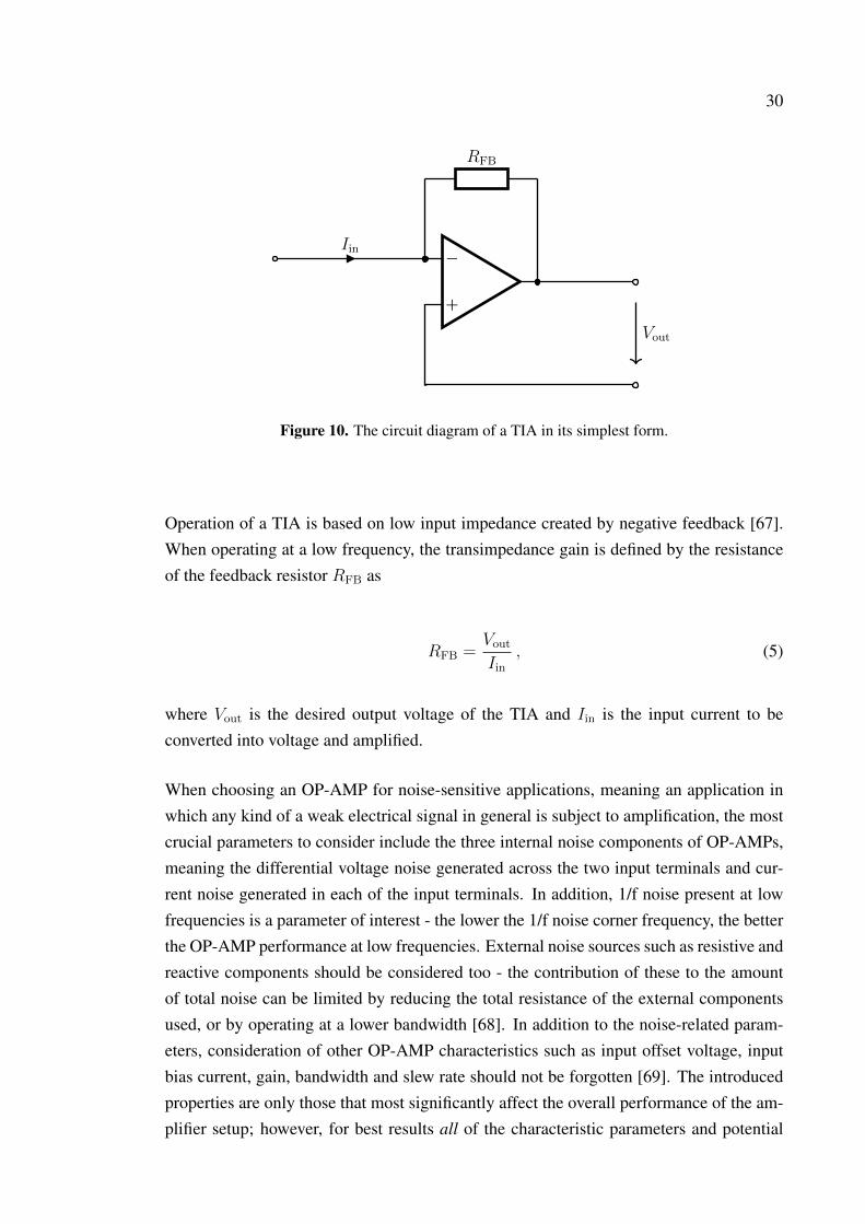
30
−
+
Iin
RFB
Vout
Figure 10. The circuit diagram of a TIA in its simplest form.
Operation of a TIA is based on low input impedance created by negative feedback [67].When operating at a low frequency, the transimpedance gain is defined by the resistanceof the feedback resistor RFB as
RFB =VoutIin
, (5)
where Vout is the desired output voltage of the TIA and Iin is the input current to beconverted into voltage and amplified.
When choosing an OP-AMP for noise-sensitive applications, meaning an application inwhich any kind of a weak electrical signal in general is subject to amplification, the mostcrucial parameters to consider include the three internal noise components of OP-AMPs,meaning the differential voltage noise generated across the two input terminals and cur-rent noise generated in each of the input terminals. In addition, 1/f noise present at lowfrequencies is a parameter of interest - the lower the 1/f noise corner frequency, the betterthe OP-AMP performance at low frequencies. External noise sources such as resistive andreactive components should be considered too - the contribution of these to the amountof total noise can be limited by reducing the total resistance of the external componentsused, or by operating at a lower bandwidth [68]. In addition to the noise-related param-eters, consideration of other OP-AMP characteristics such as input offset voltage, inputbias current, gain, bandwidth and slew rate should not be forgotten [69]. The introducedproperties are only those that most significantly affect the overall performance of the am-plifier setup; however, for best results all of the characteristic parameters and potential

31
noise sources should be considered when evaluating an OP-AMPs performance in noise-sensitive applications. [66]
In some cases, it can be wise to divide the amplifier setup into two separate stages, re-sulting in a so-called composite amplifier [70]. This kind of amplifier chaining is wellsuited for applications where a photodiode is operated [71] and can provide practical de-sign benefits, including at least the possibility of choosing an OP-AMP with good inputcharacteristics as the first stage (preferably a FET input type OP-AMP, unless operating ata high temperature, in which case a bipolar type should be considered [72]), and one withgood output characteristics as the second stage. This could possibly even help to save oncosts, for conventional OP-AMPs are typically not of good quality in terms of both inputand output characteristics.
3.2 Analog-to-digital converters
Analog-to-digital converters (ADC) are electronic components used to convert a time-continuous electrical signal into quantized, discrete format in order to create a definedconnection between a physical quantity of interest and its numerical representation. Thereare many kinds of ADCs available, designed for a wide variety of uses. Nowadays,both high-quality discrete ADCs and those integrated in MCUs, Field-ProgrammableGate Arrays, processors and system-on-a-chip devices alike, are available. Hence, it iscrucial to understand the basic operating principle of each of the most typical types ofADCs. Main types of ADCs include successive approximation register ADCs, Sigma–Delta (ΣΔ) ADCs, and pipeline ADCs. The same basic principles related to choosingelectronics of any kind and for any purpose apply to ADCs too. The first things to con-sider should be the general requirements placed for the A/D conversion by the application,as this helps to delimit the options available. These general requirements include the basiccharacteristics of ADCs, such as the sampling frequency (samples per second), accuracy(bitrate) and supply power. [73]
For the application of this thesis a moderately low sample rate is enough, as all of themeasurements included are related to functionalities with a frequency of way below 100kHz. This excludes the fastest, pipeline-type ADCs, intended to be used in completelydifferent kind of applications, from the suitable options leaving integrated and discretesuccessive approximation register ADCs and ΣΔ-ADCs. For the bitrate, 12 bits givinga theoretical maximum of 212 = 4096 different representable values, is enough. The useof ΣΔ-ADCs having a bitrate higher than 12 bits could be considered, but their price is

32
disproportionate considering the requirements of the application. Lastly, as the prototypeis intended to be powered using USB 2.0, low supply power is a must-have feature. Thisleaves the options of using either a discrete or integrated successive approximation registerADC, which is well suited for multichannel data acquisition. As an MCU is included inthe system implemented as part of this thesis anyway, it should be sensible to considerchoosing an MCU with a successive approximation register ADC of sufficient quality; allof the major microcontroller manufacturers do produce such. [73–75]
No matter how high the quality of a measurement system, its performance may be severelydegraded by A/D conversion errors. For the highly error-sensitive instrumentation ap-plications specifications for integral nonlinearity error, offset and gain errors, thermal-phenomena related effects, and AC performance should be carefully inspected. In ad-dition, it is highly preferable to estimate the overall system error by performing a mea-surement uncertainty analysis using either the root-sum-squared method or the worst-casemethod. [76]
3.3 DC voltage regulators
In electronics it is very often necessary to reduce the main supply voltage for use in thedifferent electrical subsystems. Some subassemblies of the system might run on a differ-ent operating voltage than others, or a certain very precise and time-invariant referencevoltage may be needed. Such voltage levels - lower than the main supply voltage of thesystem - can be achieved using a voltage regulator. As there are many kinds of voltageregulators available, the exact method of implementation should be chosen to best matchwith the requirements of the target subassembly. Because of this, complex electrical sys-tems typically utilize several different ways of voltage regulating.
Resistor voltage dividers are an easy and inexpensive way to create a reference voltage, orto scale a voltage to-be-measured so that it fits within the input range of an ADC. When-ever a more precise reference voltage, less sensitive to possible changes in the operatingconditions (like the ambient temperature) is needed, a discrete shunt or series voltage ref-erence should be used. If an output current larger than that of a voltage reference canprovide is required, an active voltage regulator should be used. The main types of activevoltage regulators include linear regulators and switching regulators. Linear regulatorsproduce less noise and are simpler in terms of circuit configuration, but their efficiencyis inferior to that of switching regulators, meaning that they consume a larger amountof power and thus generate a larger amount of heat - however this does not become a
33
problem if the output current is low. Even though the efficiency of switching regulators ishigher than that of linear regulators, meaning that they consume less power and generatea smaller amount of heat, the use of switching regulators should be avoided in noise-sensitive instrumentation applications, as their operation is based on rapid on/off switch-ing and more complex external circuitry - both being factors that inevitably increase thetotal amount of noise in an electronic system. [77]
3.4 Infrared signal modulation
In theory, if it was possible to exactly define the incident radiation intensity I0 (see equa-tion 1), an NDIR gas sensor could be realized using DC operating mode. However, inpractice it is necessary to modulate the carrier signal at some point of operation. This isbecause without modulation, the information on the concentration of the target gas (con-tained in the carrier signal) could not be reliably distinguished from the noise sourcesaffecting the system. Such sources of noise include, for example, ambient IR radiationand different kinds of offset errors (such as photodetector dark current and OP-AMP inputoffset) that directly affect the measurement. By modulating the IR and using algorithmsfor processing the measurement data, it is possible to minimize the effect of offset errorsto the gas measurement.
AC operating mode can be achieved, for example, by using an optical chopper or byelectrically modulating the IR source used. Moving parts typically degrade long-term sta-bility and their miniaturization is rather difficult. For this reason, the latter method, i.e.electrical modulation of the power fed to the IR source, is used in this work. Electricalmodulation of the IR source component can be implemented in many ways, for exampleby using a combination of active components and digital electronics. When modulatingthe IR source, its response time must be taken into account. Because the IR source used (aVaisala µG) is of thermal type, it has a somewhat slow response time. This is an inevitablefeature of incandescent type sources (as described in more detail in section 2.3.2). Theemitter area does not heat up and cool down instantaneously, but instead logarithmically.Thus, when using an incandescent IR source, it is necessary to use a modulation signalwith a period longer than the thermal response time of the component. Another possibleway to implement AC operating mode is to modulate the tunable optical filter, if suchis included in the system. As proposed by Ebermann et al., a faster measurement cyclecan be achieved "by fast switching or sinusoidal modulating the filter wavelength" [78].This, of course, requires that a fast enough detector is used, so that modulation of thesignal can be observed. As discussed in section 2.5, photodetectors enable the described

34
faster measurements to be performed, compared to thermal components. Modulation ofa voltage-tunable filter can be implemented, for example, by using a digitally controlledswitch to alter between any two (or more) operating voltages. Previously performed ex-periments utilizing the tunable optical filter modulation method, proposed by Ebermannet al. [78], have proven its functionality as well as its significantly fast response time.For this reason, control electronics for modulating the FPI filter are also designed for theprototype implemented as part of this thesis.
3.5 Thermoelectric cooling
Thermoelectric cooling (the operating principle of which is presented in figure 11) iscommonly used in many of the photonics-related applications to control the temperatureof various kinds of semiconductor components, such as lasers and photodiodes, to read-ings well below the natural temperature of their operating environment. Thermoelectriccooling is based on the Peltier effect, which describes the transfer of heat energy from ajunction to another in a thermocouple, where the junctions are made of materials havingunequal Seebeck coefficients. This can be considered as a mechanism opposite to theSeebeck effect, where a temperature difference ΔT creates a voltage difference acrossthe junctions of a thermocouple. In figure 11 the negative and positive charges shiftedtowards the hot surface represent the charge carrier gradient caused by the voltage acrossthe element, which in turn causes the temperature gradient. [79]
+ -
DISSIPATED HEAT
COOLED SURFACE
++
+
++
+
--
-
--
-
I
Figure 11. A diagram depicting the Peltier effect being utilized in one of its applications; thethermoelectric cooler. Direction of electric current is represented with black arrows within theelectrical conductors colored light-grey.
35
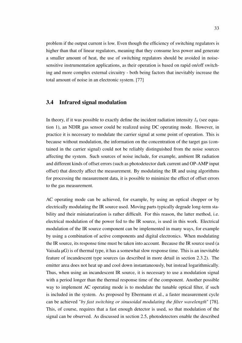
Some manufacturers produce photonic detectors that are equipped with a thermoelectriccooler (TEC), integrated inside the component package (figure 12 [80]). These integratedTEC modules make it possible to control and keep the temperature of the detector chip,placed atop of the cooler element[s], at a desired value. Multiple TEC elements can beplaced on top of each other to achieve a larger maximum temperature difference ΔTMAX
between the hot and cold sides of the TEC element. This causes the cooling to be moreefficient, as long as adequate heat removal is provided. Typical amount of cooler stagesranges from one to four and typical values of ΔTMAX for the different amounts of stagesare approximately as follows: 60 to 72 K for 1-stage setups, 80 to 100 K for 2-stagesetups, 100 to 110 K for 3-stage setups, and 110 to 130 K for 4-stage setups. Actualperformance is, however, always subject to the ambient conditions. [81]
Figure 12. A picture showing an integrated four-stage TEC module, on top of which the IRdetector is placed. The figure is retrieved from [80] under the CC-BY-NC-ND-4.0 license.
For the photodetectors with an integrated TEC module it is typical that also a thermistor,located next to the IR detector chip, is included. Thermistors with a negative tempera-ture coefficient (NTC) are more commonly used as they are well-suited for temperaturemeasurement & control applications - thermistors with a positive temperature coefficientexhibit a smaller resistance change over the same temperature range, as well as a char-acteristic switching point after which the resistance rapidly grows, making them bettersuited for applications like overcurrent protection and battery charging management [82].Resistance of a thermistor changes proportionally to its temperature. If an additional, con-ventional, resistor is introduced to form a voltage divider, the voltage across the voltage-dividing resistor changes proportionally to the temperature, too. Essentially, thermistors

36
offer a simple and inexpensive way to measure temperature; that information can then beused as a part of a control loop used to maintain a consistent temperature.
3.6 Digital control
Modern measuring instruments are complex embedded systems; mixed-signal devicesthat use a combination of both analog and digital electronics to enable data acquisitionand precise control of the measurement cycle. Typically, a mix of analog and digital elec-tronics has to be used, as the measurement data acquired is analogous in origin, but itis most often desired to be processed and displayed in digital form. These devices alsoincreasingly include Internet of Things capabilities, just like any other commercial elec-tronics nowadays. Microcontrollers can be used to introduce digital control to a systemfor the purpose of simplifying its operation. Indeed, many of the functionalities that arequite straight-forward to produce by means of digital control design would be more com-plicated to accomplish using analog electronics only, while some of the functionalitieswould be completely unreasonable to implement without the use of digital electronics &control. To sum up the potential benefits of digital control, it can significantly increasesystem flexibility, reliability and programmability in addition to simplifying the systemintegration and testing processes - all this while reducing design time and largely elimi-nating the need of discrete tuning components [83].
The most important digital control concepts regarding the application of this thesis includedifferent types of digital control signals and digital control loops. A control signal can bedefined as an electrical pulse that represents a software-defined control command [84].Commonly used control signal types which microcontrollers can typically output are, forexample, pulse-width modulated (PWM) square wave and high/low state DC voltagesproduced by General-Purpose Input/Output pins. PWM can be used for many kinds ofpurposes, such as controlling the magnitude of instrumentation-related operating volt-ages, and General-Purpose Input/Output signals for switching various active componentssuch as LED indicators ON and OFF, or for changing the position of a multi-pole digi-tal switch. In connection with this thesis, the need of control is most essentially relatedto thermoelectric cooling, introduced in section (3.5). A digital Proportional–Integral–Derivative (PID) controller is suitable for the purpose, as demonstrated by Mayursinh etal. [85]. PID controller is a closed-loop control system. It compares the set point valueof the controlled parameter (such as temperature) to a measured process variable (such asthe linearized voltage of a thermistor corresponding its temperature). In addition to PID,the use of a simpler and slower-reacting PI controller with an easier tuning procedure can

37
be considered for systems without the need for a fast response - the derivative part of aPID controller makes the system calculate the output using the information of how fastthe error term changes, which can cause problems in the form of derivative kicks if noiseis introduced to the process variable [86].

38
4 ELECTRONICS DESIGN
There would be several possible ways to implement the prototype’s desired features (de-scribed in section 1.2); various technologies and methods are feasible for creating a sys-tem that would include at least most of the subsystems and their respective functionalities.Two examples of such feasible technologies would be developing either an Application-specific Integrated Circuit (ASIC), or a system-on-a-chip. However, as Vaisala utilizes ahigh-mix low-volume strategy with an extensive product portfolio and moderate volumesper product type, there is no need to develop highly specialized and complex integrateddevices such as ASIC chips. Due to the need for flexibility and since most componentsused in the products are not purchased in large volumes, the economies of scale wouldnot be achieved, making the design and use of ASICs unnecessarily expensive. Thesekinds of solutions are indeed better suited for mass production. In addition, the workflowof ASIC chip design process is time-consuming and complicated, making developing anASIC an inappropriate approach especially in the case of a thesis. For these reasons, anddue to the fact that there are many competitive alternatives available among them, discretecomponents were used in the electronics design of the prototype. The component choicesmade were mainly based on the theory background presented in Chapter 3. The electronicschematic was designed using PADS® Logic, part of a series of electronic computer-aideddesign software released by Mentor, a Siemens Business.
Figure 13 depicts the block diagram introducing all of the main subsystems includedin the prototype. As described in section (1.2), the system consists of an MCU, an IRsource, a voltage-tunable FPI filter, an IR photodetector & a two-stage amplifier, TECdriver for cooling the detector, as well as the control electronics needed to operate allof these functionalities. In addition to the subsystems presented in the block diagram,the prototype includes operating-voltage related elements and a RS232 serial bus. Thesesubsystems, excluding the serial bus, can be viewed in the circuit diagram figures includedin each section of this chapter. Operating voltages are discussed in more detail later on insection (4.7).

39
Photodetector
Vaisala
Voltage-
Tunable
FPI filter
Vaisala μG
IR Source &
Fixed-BP
Filter
μG Control
Electronics
FPI Filter
Control
Electronics
NTC
Thermistor
(inside the
photodetector
package)
TEC Control
Electronics
(ADN8833)
Thorlabs
TED200C
T-controller
(optional)
TEC (inside
the photo-
detector
package)
JTAG
Debug Port
RS232
Serial Port
1st Stage
Amplifier
2nd Stage
Amplifier
IR r
adia
tion
MICROCONTROLLER UNIT
Enable &
Control Signal
Meas.
SignalsGPIO,
PWM Output,
Analog Inputs
Meas.
SignalAnalog Input
Analog Input
Meas.
Signal
Meas.
Signals
Control
Signals
Control
Signal
Meas.
Signals
PWM Outputs,
Analog Inputs
PWM Output,
Analog Inputs
2V
5
Ref
eren
ce
Operating
Power
Operating
Power
Operating Voltage
Operating Power
Raw
Signal
2V5 ReferenceVREF+
TDI, TDO,
TMS, TCK,
TEST, RST
UCA0TXD,
UCA0RXD,
UCA1STE,
UCA1CLK
Figure 13. Block diagram of the designed prototype. For the sake of clarity, the block diagram issimplified so that operating voltages of the different subsystems are not shown.
As two detectors, different both by their electrical and mechanical characteristics as in-troduced further on in section (4.3), were used to test the operation of the prototype, twoslightly different design variants were produced. Especially the difference in the mechan-ical design of the detector packages placed unique requirements for both of the detectortypes tested.
Notice is hereby given that part of the electrical circuits used and presented in this chapterare designed by other Vaisala engineers. For such subsystems, the original designers ofthe circuits are referred to either in the captions of the circuit diagram figures, or in thetext content describing the subsystem if no figure of the subsystem is presented.

40
4.1 Passive components
This section presents the justification for the choice of types of general-purpose passivecomponents used, including resistors, capacitors and inductors. The photodetectors cho-sen, classifiable as passive components depending on the definition used, are consideredlater on in section (4.3). Resistors, capacitors and inductors were chosen taking intoaccount the different requirements per and within each subsystem including them. Char-acteristics considered for all of the passive component categories include temperature de-pendency, noise-related performance, precision and surface-mount device package type.Whenever possible, an attempt was made to favor the use of components that are alsoused in other electronics designs made by Vaisala. To limit the bill of materials, samepassive component values were used as often as possible in the different subsystems.
For passive components within signal paths - such as resistors and capacitors used foramplifier feedback or filtering - components with high precision and low temperature de-pendency were chosen. As for the component package sizes of the passives; most ofthem are encased in an imperial 0603 (dimensions 1.55 × 0.85 × 0.45 mm [87]) pack-age or larger, and the prototype contains component packages no smaller than the sizeof imperial 0402 (dimensions 1.00 × 0.50 × 0.35 mm [87]). There would have been noreason whatsoever to use components smaller than that for early stage prototyping. Thisis because there were no significant requirements considering the size of the prototype,and because the precision and overall performance of passive components typically de-creases with package size. In addition, it was desired that the components could be easilyreplaced by manual soldering, if needed. Hand soldering components having a packagesize smaller than 0402 would require excessive expertise and practical experience, as wellas vision-enhancing equipment, such as microscopes, to be used to assist in the solderingprocess.
4.2 Control of infrared source & tunable optical filter
Two separate circuits are used to operate the Vaisala µG IR source and the Vaisala voltage-tunable FPI filter, both located inside the same hermetically sealed 4-lead TO-5 compo-nent package. Both of the circuits presented in this section are designed by other Vaisalaengineers, but their operation had to be described as they play an important role in theoperation of the prototype. The power fed to the Vaisala µG IR source is controlled usinga switching metal–oxide–semiconductor field-effect transistor operated with an ampli-

41
fied, low-pass filtered, PWM control signal. Voltage over the µG and the current flowingthrough it are measured to get information of the amount of power consumed. The controlelectronics used to operate the µG IR source are designed by Senior Electronics EngineerNiskanen A. of Vaisala.
Circuit diagram of the FPI filter control circuit can be seen in figure 14. The AnalogDevices ADG839 (A7), a single-pole double-throw switch, is used to modulate the FPIfilter between any two voltages within the range of 0 to 30 V in order to alter the pass-bandof the filter between selected wavelength bands corresponding the two operating voltageschosen. The position of the switch (A7) is controlled using one of the General PurposeInput/Output pins of the MCU.
(a) Two Butterworth low-pass filters. (b) Control electronics for the FPI filter.
Figure 14. (a) shows the active low-pass filters used to produce the two operating voltages forthe FPI filter and (b) is the electronic schematic of the FPI filter control electronics. Both of thesecircuits are designed by Research Scientist Huuhtanen M. of Vaisala.
In the subfigures (a) & (b) of figure 14, reference designators V1 & V2 represent thetwo voltage levels used to drive the FPI filter’s pass-band to different wavelength bands.Capacitors C30, C31, C43, C67 are used to filter electronic noise.
4.3 Infrared photodetectors
Two photovoltaic detector samples were alternately used to test the operation of the pro-totype: a VIGO System PVIA-2TE-5 and a Hamamatsu Photonics P13243-222MS. Theyare presented in this section, limiting the review to the basic features and electrical prop-erties of them, as well as the mechanical properties of the component housing (specific toboth of the detectors tested).

42
The detectors are mounted to the PCBs using pin receptacles manufactured by Mill-Max(mfr. part no. 4015-0-43-80-30-27-10-0). The use of pin receptacles allows the com-ponents to be easily attached and detached without soldering, which could potentiallydamage the detectors as they are sensitive to high temperatures. These particular pin re-ceptacles were chosen as they take up only a very small area of the circuit board and matchwith the cross-sectional area of the component leads of both of the detector types tested.The number of pin sockets added to the design matches the number of component leadsused. In other words, sockets are not added for unused leads of the component packagesfor this would incur unnecessary costs. In addition to mounting the detectors, the samepin receptacles are used to mount the TO-5 package housing the Vaisala IR source & FPIfilter, discussed in section (4.2), too.
4.3.1 Detector type 1: VIGO System PVIA-2TE-λopt
The VIGO System PVIA-2TE-λopt is a product family of photovoltaic IR detectors withan integrated 2-stage TEC element, and an optional hyperhemispherical (or hemispheri-cal) immersion lens which is used to boost the optical gain of the detector to improve itsSNR. Also included inside the package is a set of water absorbers, that prevent conden-sation of water vapor in the case of rapid temperature changes. Most of the propertiesare customizable upon customer request; for example it is possible to choose an opticalwindow with a wedged profile, meaning that the upper surface of the window is non-perpendicular to the angle of incidence of the incoming radiation. This feature helps toprevent direct backscatter which can cause changes in performance, or even optics dam-age in applications utilizing a high-power source like a laser. The λopt in the detectorproduct code denotes the optimal wavelength (i.e. the wavelength with highest minimumguaranteed D*) in µm - versions ranging from an optimized wavelength of 3 µm to 10.6µm are available as standard. Other characteristics presented in the datasheet include
D* for λpeak and λopt, current responsivity length product Ri·L at λopt [A ·mm
W], time
constant τ [ns], and resistance optical area product R·A [Ω · cm2]. [88]
PVA-2TE-5AR (figure 15) was selected as the 1st detector alternative for testing the pro-totype designed. The variant chosen features an optical area of 0.10 × 0.10 mm and afield of view of 70° with no immersion. The component package chosen is a hermeticallysealed 12-pin straight-edged TO-8 with a threaded fastening bolt located at the middle ofthe bottom surface. The bolt can be used to attach a heat sink when the integrated TECelement is used, more of which later on in section (4.5.4). The TO-8 package is sealedusing a wedged window made of anti-reflection coated aluminum oxide (Al2O3). [88]
43
Figure 15. A photograph of the detector type 1: VIGO System PVIA-2TE-5.
The integrated 2-stage TEC element is capable of cooling the detector down to a temper-ature of approximately 230 K in favorable operating conditions, noting that the declaredΔTmax of the device is 92 K. Maximum values for the operating voltage and current are1.3 V and 1.2 A, respectively. This gives the theoretical maximum cooling capacity Qmax
of 360 mW. A Murata NCP03XM222E05RL NTC thermistor is placed on top of the TECelement, next to the detector chip, to allow temperature monitoring and implementationof a temperature control system. To improve the performance of the integrated TEC, aswell as to protect the detector chip from harmful contaminants as described in section(2.5), the component package is filled with a mixture of dry noble gases with low thermalconductivity. [88]
4.3.2 Detector type 2: Hamamatsu Photonics P13243
The Hamamatsu Photonics P13243 is a series of photovoltaic detectors designed for gasdetection, radiation thermometer and flame detection applications. The series featuresdetectors with high sensitivity and a fast response. Variants both with and without a TECelement (having a maximum amount of four stages) are available. As standard, two dif-ferent optical window materials - silicon with anti-reflecting coating, and pure sapphire -are available. Hamamatsu Photonics offers the possibility of customizing the componentpackage as well as the optical filters and lenses used. The spectral response is optimized

44
over the range of between about 2 to 5 µm slightly depending between the variants avail-able, however peak detectivity should occur at 4.1 µm regardless of the version. The mainoptical and electrical characteristics declared in the datasheet include D* for the peak sen-sitivity wavelength λp, photosensitivity S at λp [mA/W, V/W], minimum and typical shuntresistance Rsh [kΩ], typical and maximum noise equivalent power NEP at λp [W/
√Hz]
and typical rise time tr [ns]. [89]
P13243-222MS (figure 16) was selected as the 2nd detector alternative for testing theprototype designed. It has a photosensitive area of 0.70 × 0.70 mm and a field of view of113°. The package solution chosen is a conventional 6-pin TO-8 with a brim wider thanthe main mechanical body, located at the junction of the package cap and bottom. Theoptical window enclosing the TO-8 package is made of sapphire. [89]
Figure 16. A photograph of the detector type 2: Hamamatsu Photonics P13243-222MS.
The ratings given for the integrated 2-stage TEC element are as follows. In ideal con-ditions the temperature difference between the cool and hot surfaces can reach 70 K. Ina typical room temperature of 298 K, the lowest reachable element temperature is 243K, with a ΔTmax of 55 K. The TEC element should be operated at most with 1 V max-imum voltage and 1 A maximum current, and a heat sink with a thermal resistance of 3°C/W is recommended. A built-in NTC thermistor (with specifications given in [89]) isincluded and located atop the TEC element and close to the detector chip, to allow forimplementation of a temperature control system. [72]

45
4.4 Photodetector signal amplification
As photovoltaic-mode photodetectors produce only a very weak current signal and it wasdesired that the measurement signal would be eventually converted into digital formatusing an ADC, an amplifying current-to-voltage conversion was required. A chainedtwo-stage OP-AMP configuration consisting of a TIA followed by an inverting OP-AMPcircuit is used for the purpose.
4.4.1 Stage 1: transimpedance amplifier
The current signal produced by the IR photodetector (4.3) is first amplified and convertedinto a voltage signal. Analog Devices LTC2057 was chosen as the OP-AMP of the 1st
stage (figure 17). It is a low-noise, zero-drift precision OP-AMP designed for measure-ment and instrumentation systems, with proposed applications ranging from low-side cur-rent sensing to high resolution data acquisition. The component meets most of the essen-tial requirements, such as input-performance related criteria, set out in the theoreticalbackground section (3.1) discussing OP-AMPs. [90]
Figure 17. A screenshot of the electronic schematic, showing the 1st stage of the amplifier setup.Signal paths marked with dashed lines indicate that the circuit continues outside the figure.

46
The positive input terminal of the OP-AMP is provided with a reference voltage of 1.25 V,created using a high-precision resistor voltage divider, in order to operate within the dy-namic range of the ADC. Other component values for the TIA configuration were selectedbased on the Texas Instruments application note SLAA926A [91]. First, the resistance ofthe gain resistor (R2 in figure 17) was set by equation
R2 =VoMax − VoMin
IiMax
, (6)
where VoMax is the desired maximum output voltage, VoMin is the desired minimum outputvoltage, and IiMax is the maximum input current.
The maximum output and input voltages were selected taking into account the input rangeof (and the reference voltage set for) the ADC used. The maximum and minimum outputvoltages VoMax and VoMin were initially set to 1.75 V and 0.75 V, respectively. For themaximum input current IiMax, a much-underestimated initial guess of 1.5 µA was cho-sen. Consequently, the resistance of the gain resistor was initially set to 680 kΩ. Theselected feedback resistor is 0603 (imperial) in size and could thus be easily changed byhand in case the magnitude of the gain needs to be altered. It should be noted that as theshunt/series resistance of the detector types 1 and 2 is different, a different 1st stage feed-back resistance value should be used for the detectors for optimal performance. This isbecause if the feedback resistance exceeds the detector’s shunt resistance, the input noise
& offset voltages of the OP-AMP will be multiplied by 1 +Rf
Rsh
, causing degraded per-
formance [72]. However, to simplify fabrication, each circuit board is initially furnishedwith the same resistors. From the point of view of SNR the value of the feedback resis-tance is insignificant, as both the signal and all the noise terms are equally amplified. Thefeedback capacitor (C8 in figure 17) should be chosen so that it meets with the circuitbandwidth, using equation
C8 ≤1
2 · π ·R2 · fp≤ 1600 pF , (7)
where R2 is the resistance calculated using equation (6) and fp is the closed-loop band-width. A capacitor with the nominal value of 220 pF was chosen as the feedback capacitorC8 in order to form a passive low-pass RC filter together with resistor R2, having a cutofffrequency of approximately 1 kHz. As the application is not high-frequency in terms ofthe signals present in the system and the electronics used (the prototype operates belowthe frequency of 100 kHz), the adequacy of the OP-AMP gain bandwidth should not cause

47
any concern. Lastly, since the TIA configuration is based on creating a low-impedanceinput, a similar kind of low-impedance operating point is also required at the node com-bining the anode of the photodetector, R31, and R32 to the non-inverting input terminalof the first stage OP-AMP A3. This was accomplished by placing C4, a 3.3 µF capacitor,in between that node and the analog ground. Capacitor C9 is used to filter high-frequencynoise off the supply voltage of A3.
4.4.2 Stage 2: inverting amplifier
After the current-voltage conversion, the measurement signal of the photodetector has tobe further amplified (or scaled) in order to make it efficiently readable by the ADC of theMCU (4.6). The 2nd stage (figure 18) is implemented using a conventional inverting OP-AMP configuration, and it utilizes a Texas Instruments OPA180 which is a near zero-drift,high-precision OP-AMP with a close to rail-to-rail output swing.
Figure 18. A screenshot of the electronic schematic, showing the 2nd stage of the amplifier setup.Signal paths marked with dashed lines indicate that the circuit continues outside the figure.
Before the measurement signal enters the 2nd stage of the amplifier, the DC componentof the signal is decoupled using C11, a 2.2 uF capacitor. This capacitor together withR38 also forms a passive high-pass RC filter with a cutoff frequency of approximately70 Hz. Again, the positive input terminal of the OP-AMP is provided with a referencevoltage of 1.25 V, similarly to the 1st stage. The gain of the 2nd stage was initially set

48
to 10 by resistors R42 and R38, using equation (3). As with the 1st stage, a passive low-pass filter having a cutoff frequency of about 1 kHz was realized by connecting a 15 nFfeedback capacitor C28, parallel to the feedback resistor R42. Capacitor C13 is used tofilter high-frequency noise off the supply voltage of A4, and connector X2 is a horizontalPCB-mounted SubMiniature version A type coaxial connector that makes it possible toeasily observe the waveform of the amplified photodetector signal using an oscilloscope.Lastly, reference designator DET_MEAS carries the measurement signal to an analoginput of the MCU.
4.4.3 Design verification by simulation
The simplified operation of the amplifier setup was simulated using LTspice®, an open-source electronic circuit Simulation Program with Integrated Circuit Emphasis originallyreleased by Linear Technology Corporation, part of Analog Devices from March 2017onwards. In the simulation performed, both of the amplification stages were combinedto form the full 2-stage amplifier setup. The simulation was done using models providedby the manufacturers of the OP-AMPs used. Equivalent circuits of the photodetectorsused were not created as some of the required parameters were unavailable. Instead, thecurrent produced by the photodetector was simulated ignoring any non-idealities, usinga sinusoidal current source with a peak-to-peak current value of 50 nA as the test signal.Output of the simulation performed can be seen in figure 19.
Figure 19. The simulated photodetector signal before (blue) and after the 1st (green) and the 2nd
(purple) amplification stages.
The simulation performed was highly idealized and simplified, and was done to examine

49
merely the fundamental operation of the designed amplifier circuit. It should be noted thatthe simulation did not consider many of the aspects crucially related to amplifier design.
4.5 Detector temperature control
As a novel feature, detector temperature control electronics were designed. The temper-ature control system (figure 20) used to control the temperature of the detector’s inte-grated TEC element was implemented using ADN8833, a monolithic ultracompact high-efficiency TEC controller manufactured by Analog Devices, Inc. [92]. ADN8833 is thesoftware-controlled variant of the ADN883X family, subcategory of the Analog DevicesTEC Controller product category. The controller is operated with a digital control loop.It should be sensible to choose the software-oriented variant of the device as an MCU(presented in section 4.6) capable of controlling it is included in the prototype. In ad-dition, choosing a relatively recently released single-chip solution developed by a large-scale manufacturer should also support possible future productization of the device, as thelong-term availability is likely better secured compared to the small-scale manufacturersoffering similar kinds of solutions.
Figure 20. A screenshot showing the electronic schematic of the TEC temperature control circuit.In addition to the ADN8833 TEC driver and the passive components needed to operate it, thecircuit includes active filtering of the control signal and a screw terminal input for an externalpower supply.
The functionalities of the ADN8833 include a patented single-inductor architecture, TEC

50
voltage and current monitoring, possibility of setting the maximum voltage and currentused for cooling, as well as a 2.50 ± 0.025 V reference output. Chapters Theory of
Operation and Applications Information of the ADN8833 datasheet were used as a basisfor the electronics design associated with the component. [92]
Selection of the passive components related to the driver’s input and output, as well asgeneral electromagnetic interference filtering (including inductor L5 and capacitors C40,C41, C42, C51 and C52), was done according to the application information provided inthe ADN8833 datasheet [92]. Test points TP27-1 and TP31-1 are plated through-holesthat allow conducting the TEC driver’s output off the circuit board with wires soldered tothe test points - this feature was used during development of the associated digital controlloop, and for experimentally testing the operation of the controller.
4.5.1 General setup
The desired limit of the maximum TEC voltage was set by a resistor voltage divider usingthe following equations:
VTEC_MAX_COOLING = VVLIM_COOLING · AVLIM , (8)
where VTEC_MAX_COOLING is the desired voltage limit of 1.0 V and AVLIM = 2 V/V. Fromequation (8) it was then solved that VVLIM_COOLING = 0.5 V. [92]
VVLIM_COOLING =VREF ·RR68
(RR69 +RR68), (9)
where VVLIM_COOLING is 0.5 V as calculated using equation (8), VREF is the ADN8833’sinternal reference voltage of 2.5 V, and RR69 is a preselected resistance value of 36.5kΩ. With these parameters, the required resistance RR68 was solved; its value should beapproximately 9.1 kΩ. [92]
The maximum TEC current limit was set starting from the following equation:
ITEC_MAX_COOLING =VILIMC − 1.25 V
RCS
, (10)

51
where ITEC_MAX_COOLING is the preferred TEC current limit of 0.8 A given in the appli-cation notes for the sample detectors 1 & 2 [72, 93], and RCS is the TEC driver’s internalcurrent sink resistance of 0.285 V/A. The value of VILIMC could then be solved; it is equalto 1.67 V. [92]
Then, by combining equations
VILIMC = VILIMH + ISINK_ILIM ·
(RR21 ·RR9
RR21 +RR9
)VILIMH = VREF ·
RR9
RR21 +RR9
(11)
a simplified form was obtained:
VILIMC =VREF ·RR9
RR21 +RR9
+ ISINK_ILIM ·(RR21 ·RR9
RR21 +RR9
), (12)
where VREF is the ADN8833’s internal reference voltage of 2.5 V, RR21 is a generic re-sistance value 100 kΩ selected for R21, and ISINK_ILIM is the 40 µA current drawn bythe internal current sink of the ADN8833. Finally, the suitable resistance value RR9 forthe second resistor R9 (part of the voltage divider defining the maximum TEC current incooling mode) could be solved; it should be approximately 34.4 kΩ. [92]
For easy monitoring of the actual voltage over the TEC and the current flowing throughit, the ADN8833 includes analog outputs VTEC and ITEC with voltages proportional totheir corresponding quantities. Equations used to convert the voltages of VTEC and ITECinto the actual voltage across the TEC and the actual current flowing through it are
(VLDR − VSFB) =
VVTEC − 1.25
0.25
ILDR =VITEC − 1.25
RCS
(13)
where the subtraction of the linear driver output voltage and the PWM TEC driver output(VLDR−VSFB) equals to the voltage over the TEC, ILDR is the current output of the lineardriver (i.e. the current flowing through the TEC), and RCS is the current sense gain of0.525 V/A. A voltage of 1.25 V on the VTEC and ITEC pins corresponds to a situationwhere the voltage across the TEC is 0 V and the current flowing through it is 0 A. [92]
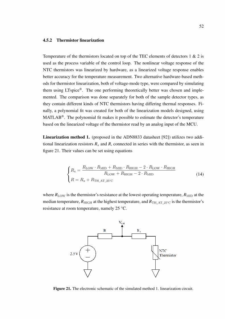
52
4.5.2 Thermistor linearization
Temperature of the thermistors located on top of the TEC elements of detectors 1 & 2 isused as the process variable of the control loop. The nonlinear voltage response of theNTC thermistors was linearized by hardware, as a linearized voltage response enablesbetter accuracy for the temperature measurement. Two alternative hardware-based meth-ods for thermistor linearization, both of voltage-mode type, were compared by simulatingthem using LTspice®. The one performing theoretically better was chosen and imple-mented. The comparison was done separately for both of the sample detector types, asthey contain different kinds of NTC thermistors having differing thermal responses. Fi-nally, a polynomial fit was created for both of the linearization models designed, usingMATLAB®. The polynomial fit makes it possible to estimate the detector’s temperaturebased on the linearized voltage of the thermistor read by an analog input of the MCU.
Linearization method 1. (proposed in the ADN8833 datasheet [92]) utilizes two addi-tional linearization resistors Rx and R, connected in series with the thermistor, as seen infigure 21. Their values can be set using equations
Rx =RLOW ·RMID +RMID ·RHIGH − 2 ·RLOW ·RHIGH
RLOW +RHIGH − 2 ·RMID
R = Rx +RTH_AT_25°C
(14)
where RLOW is the thermistor’s resistance at the lowest operating temperature, RMID at themedian temperature, RHIGH at the highest temperature, and RTH_AT_25°C is the thermistor’sresistance at room temperature, namely 25 °C.
Figure 21. The electronic schematic of the simulated method 1. linearization circuit.

53
Two different combinations of resistances Rx and R, calculated using equation (14) androunded to the nearest genuine resistor values, were simulated. The resistor combinationssimulated are listed in Table 2.
Table 2. Resistance value combinations used to simulate linearization method 1.
Combination Rx (Hamamatsu / VIGO) R (Hamamatsu / VIGO)
1 19.3 kΩ / 6.57 kΩ 43.7 kΩ / 14.5 kΩ (Rth at 25 °C)
2 19.3 kΩ / 6.57 kΩ 28.4 kΩ / 8.75 kΩ (Rth at 0 °C)
Linearization method 2. (proposed in the Texas Instruments Application Report SNOAA12[94]) utilizes two additional linearization resistors as well, but in a different configurationseen in figure 22. The first resistor Rs is connected in series with the parallel connectionof the second resistor Rp and the thermistor.
Figure 22. The electronic schematic of the simulated method 2. linearization circuit.
Two different combinations of resistances Rs and Rp were simulated; the resistor combi-nations simulated are listed in Table 3.
Table 3. Resistance value combinations used to simulate linearization method 1.
Combination Rs (Hamamatsu / VIGO) Rp (Hamamatsu / VIGO)
1 12.1 kΩ / 4.00 kΩ 24.3 kΩ / 8.00 kΩ (Rth at -5 °C)
2 10.7 kΩ / 3.28 kΩ 19.3 kΩ / 6.55 kΩ (Rth, full T-range)
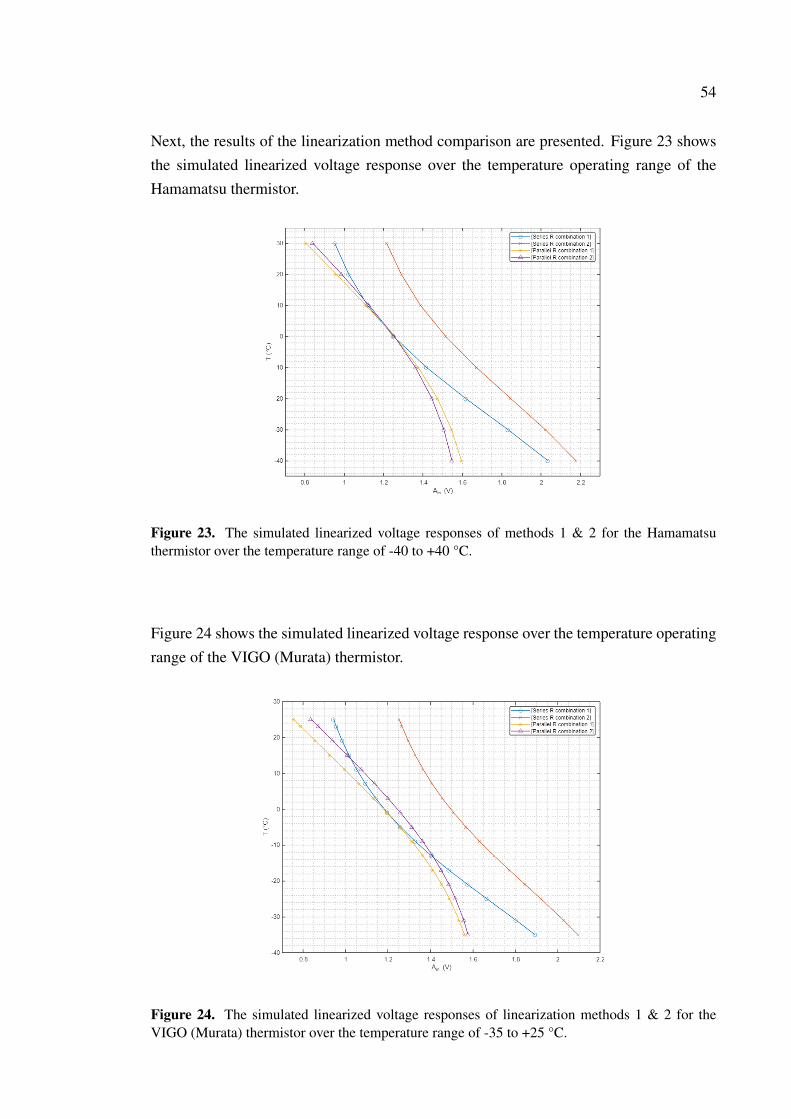
54
Next, the results of the linearization method comparison are presented. Figure 23 showsthe simulated linearized voltage response over the temperature operating range of theHamamatsu thermistor.
Figure 23. The simulated linearized voltage responses of methods 1 & 2 for the Hamamatsuthermistor over the temperature range of -40 to +40 °C.
Figure 24 shows the simulated linearized voltage response over the temperature operatingrange of the VIGO (Murata) thermistor.
Figure 24. The simulated linearized voltage responses of linearization methods 1 & 2 for theVIGO (Murata) thermistor over the temperature range of -35 to +25 °C.

55
As seen in figures 23 and 24, linearization method 1. with resistance combination 1 givesthe steepest slope for the output voltages between the temperature end points; 0.95 Vto 2.05 V for the Hamamatsu thermistor, and 0.95 V to 1.9 V for the VIGO (Murata)thermistor. This means that largest portion of the ADC’s input range is utilized. In ad-dition, highest linearity over the low end of the temperature range is achieved. Resultsof the comparison performed thus show that linearization method 1. should work bestfor the thermistors of both detectors - hence, method 1. with the better-performing resis-tance combination was chosen and implemented. The temperature of the thermistor canthen be easily calculated by measuring Vout of figure 21 and using an nth degree polyno-mial curve fitting by saving the fitted polynomial coefficients in the MCU’s ferroelectricsemiconductor random-access memory. Another way of implementing the temperatureestimation would have been utilizing the Steinhart–Hart equation. The equation containsa natural logarithmic operation and using it would thus have required excessive computingpower or storing a large lookup table of over 60,000 entries (instead of the few polyno-mial coefficients) in the memory of the MCU, making the implementation unnecessarilycomplex.
4.5.3 Control signal filter
The digital temperature control loop is closed by feeding a DC control signal to the CONTpin of the ADN8833. As the MCU used (4.6) does not include an integrated Digital-to-Analog Converter, a low-pass filtered PWM signal, produced by the MCU, is used asthe control signal defining the output of the TEC driver. Optionally, a discrete Digital-to-Analog Converter could have been used, but this would have unnecessarily increasedthe complexity as well as the total cost of the system. The unity-gain Sallen–Key low-pass filter designed for the purpose of control signal filtering can be seen in figure 25.After filtering the PWM, the remaining DC-component with minimized ripple, acting asthe control signal, is applied to the CONT pin of the ADN8833 (figure 20). The controlsignal voltage at the CONT pin has to be chosen from between 0 V and 2.5 V (due to theADN8833 internal 2.5 V reference) according to the desired voltage over the controlledTEC element. Voltage of the filtered control signal can be varied by changing the dutycycle of the initial PWM control signal. When designing a DAC filter, a compromise hasto be made between the maximum rate of change of the filtered DC voltage and the peak-to-peak magnitude of the residual ripple of the DC voltage. A higher cutoff frequencyallows for faster rate of change, whereas a lower cutoff frequency reduces the ripple.As the process variable (temperature) has a rather slow rate of change, low ripple waspreferred over speed.

56
Figure 25. An enlargement of figure 20 showing the circuit diagram of the unity-gain Sallen–Keylow-pass filter used to convert the MCU’s PWM output to a digital-to-analog converted output.
For the -3 dB corner frequency fc of 1 kHz, the required resistance values (R40 & R41)were calculated using equation
fc =1
2 · π ·√
R40 · R41 · C12 · C18, (15)
where both C12 and C18 were set to 100 nF, resulting to a required resistance of approxi-mately 16 kΩ for both of the resistors R40 and R41 [95]. Capacitor C10 seen in figure 25is used to filter high-frequency noise off the supply voltage of A10.
4.5.4 Heat dissipation
As thermoelectric coolers inevitably produce heat while being used for cooling, as de-scribed in (3.5), there is a need to dissipate the generated heat away from the componentpackage and the PCB. For the TEC elements of the detectors used in the prototype, anestimated maximum heat dissipation of 0.5 W/cm2 is required. Proper heat dissipationis crucial for reaching the desired temperature set point at the cold side of the TEC ele-ment [72, 93]. The detectors used are quite similar in terms of requirements for thermaldesign because both are enclosed in a TO-8 metal can package similar in size, and theTEC elements are placed so that their hot side is in contact with the bottom surface of thecomponent package (see IR Detectors Users Guide [93] for detector type 1, and Char-
acteristics and use of infrared detectors [72] for detector type 2). Thus, both of them
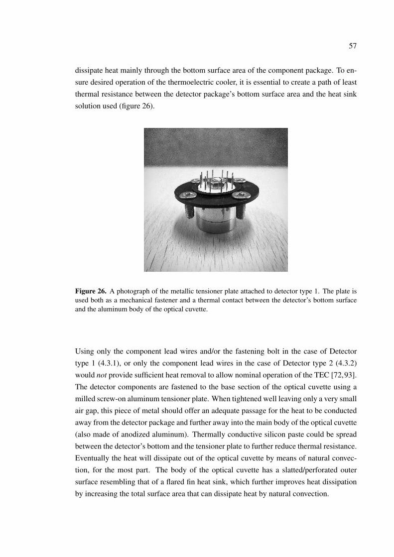
57
dissipate heat mainly through the bottom surface area of the component package. To en-sure desired operation of the thermoelectric cooler, it is essential to create a path of leastthermal resistance between the detector package’s bottom surface area and the heat sinksolution used (figure 26).
Figure 26. A photograph of the metallic tensioner plate attached to detector type 1. The plate isused both as a mechanical fastener and a thermal contact between the detector’s bottom surfaceand the aluminum body of the optical cuvette.
Using only the component lead wires and/or the fastening bolt in the case of Detectortype 1 (4.3.1), or only the component lead wires in the case of Detector type 2 (4.3.2)would not provide sufficient heat removal to allow nominal operation of the TEC [72,93].The detector components are fastened to the base section of the optical cuvette using amilled screw-on aluminum tensioner plate. When tightened well leaving only a very smallair gap, this piece of metal should offer an adequate passage for the heat to be conductedaway from the detector package and further away into the main body of the optical cuvette(also made of anodized aluminum). Thermally conductive silicon paste could be spreadbetween the detector’s bottom and the tensioner plate to further reduce thermal resistance.Eventually the heat will dissipate out of the optical cuvette by means of natural convec-tion, for the most part. The body of the optical cuvette has a slatted/perforated outersurface resembling that of a flared fin heat sink, which further improves heat dissipationby increasing the total surface area that can dissipate heat by natural convection.
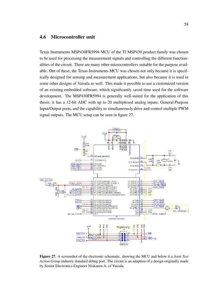
58
4.6 Microcontroller unit
Texas Instruments MSP430FR5994 MCU of the TI MSP430 product family was chosento be used for processing the measurement signals and controlling the different function-alities of the circuit. There are many other microcontrollers suitable for the purpose avail-able. Out of these, the Texas Instruments MCU was chosen not only because it is specif-ically designed for sensing and measurement applications, but also because it is used insome other designs of Vaisala as well. This made it possible to use a customized versionof an existing embedded software, which significantly saved time used for the softwaredevelopment. The MSP430FR5994 is generally well-suited for the application of thisthesis; it has a 12-bit ADC with up to 20 multiplexed analog inputs, General-PurposeInput/Output ports, and the capability to simultaneously drive and control multiple PWMsignal outputs. The MCU setup can be seen in figure 27.
Figure 27. A screenshot of the electronic schematic, showing the MCU and below it a Joint TestAction Group industry standard debug port. The circuit is an adaption of a design originally madeby Senior Electronics Engineer Niskanen A. of Vaisala.

59
The MCU is packed in a compact 48-pin Very Thin Quad Flat Non-Leaded package witha thermal pad at the package’s bottom surface. In addition to the MCU itself, the setupincludes a Joint Test Action Group industry standard debug port (connector X4) and ared LED indicator (V9), as well as an external 16 MHz crystal oscillator. CapacitorsC16, C17, C47, C72, C73, C82, C83, and C90 (seen in figure 27) are used to filter elec-tronic noise, if such would ever enter the system caused by, for example, any kind ofan unexpected transient event. The pins left unused are connected to test points makingtheir deployment possible in the event of an undesirable design error or other unexpectedneed. The pin configuration of the MCU, supplemented by additional notes regarding theoperation of the MCU, can be reviewed in Appendix 1.
The built-in multi-channel 12-bit successive approximation register ADC of the MCU isused for the A/D conversion of the amplified measurement signal from the detector and allthe other measurements necessary for operating and controlling the prototype. The ADCis fully configurable by embedded software. Using the MCU’s peripheral ADC modulereduces overall system cost as well as the surface area required for the PCB layout [96].The input range of the ADC is set by the embedded software to between 0 V and 2.5V using the MCU’s internal reference. Sampling frequency and sample count of theADC can be set by sending a command to the MCU, which allows the user to choose themeasuring interval.
4.7 Supply & operating voltages
Two alternative inputs exist for providing the main supply voltage of 15 V required tooperate the prototype. The inputs are implemented using a generic screw terminal con-nector that allows using a laboratory power supply unit, and a 4-pin M4 female connectorto which a Vaisala USB cable (part no. 219690) can be attached to in order to powerthe prototype using USB connection. The electronics related to the serial bus commu-nication are designed by Senior Electronics Engineer Niskanen A. of Vaisala. Poweringmost of the prototype using USB connection should be a convenient choice as a serialport connection is included and used in any case, as the MCU is commanded and mea-surement data is logged via the serial bus using a personal computer. For the majority ofthe prototype’s subsystems the 500 mA current delivery capability of USB 2.0 is abovesufficient. However, the current demand of the ADN8833 TEC controller is above the500 mA current output capacity of USB 2.0 because of the set maximum TEC currentlimit of the detector TEC elements, described in section (4.5). Hence, the temperaturecontrol electronics had to be powered using an additional input option. An external labo-

60
ratory power supply unit was chosen to be used for the purpose. Having separate powersupplies for the low-power signal conditioning electronics and the relatively high-powerTEC driver should also help in reducing potential issues related to electronic noise causedby electromagnetic interference.
The 15 V main supply voltage applied to the prototype has to be regulated to severalsmaller voltage levels in order to make it suitable to be used as the operating voltage ofthe different functional electrical subsystems included. This applies to all subassembliesof the prototype, excluding the supply voltage of the TEC driver, which can be set bythe user in the laboratory power supply unit that is connected to the supply voltage screw-terminal input of the TEC driver circuit. Where necessary, regulating the supply voltage isdone using Texas Instruments LP2951ACMM-3.3/NOPB low-dropout voltage regulatorunits with a programmable output [97]. An exemplary circuit diagram of one of thevoltage regulator setups used can be seen in figure 28.
Figure 28. The voltage regulator circuit used to regulate the voltage from 12 V to 3.5 V. This samevoltage regulator, manufactured by Texas Instruments, is used to accomplish all of the requiredoperating voltages by modifying the voltage divider formed by resistors R49 and R24.
The required regulated voltage levels in order of magnitude are 3.3 V, 3.5 V, 8.0 V and11.5 V. As 3.3 V is the nominal output voltage of the regulator used, output modificationis not needed in the case of this regulated voltage level. Resistor values for the outputvoltage dividers used to obtain the other required voltage levels were calculated using

61
VOUT = VREF · (1 +RR49
RR24
) + IFB ·RR49 , (16)
where VREF is the regulator’s internal nominal reference voltage of 1.235 V and IFB isthe regulator’s -20 nA nominal bias current for pin no. 7 (FB) [97]. For each of the reg-ulators, the resistance value for the resistors corresponding resistor R24 was calculatedby first choosing a general resistance value for the resistors corresponding R49. Func-tions executable using pins no. 2 (SENSE), 5 (ERR) and 6 (V TAP ) are not used andare thus left floating as recommended in the component’s datasheet [97]. In addition tothe regulated voltage levels, one voltage level higher than the 15 V main supply voltagelevel is required; the control electronics of the FPI filter (4.2) need a supply voltage of34 V, which is implemented by using a customized multi-stage Dickson charge pumpconstructed using discrete components. The charge pump circuit is designed by SeniorElectronics Engineer Niskanen A. of Vaisala.
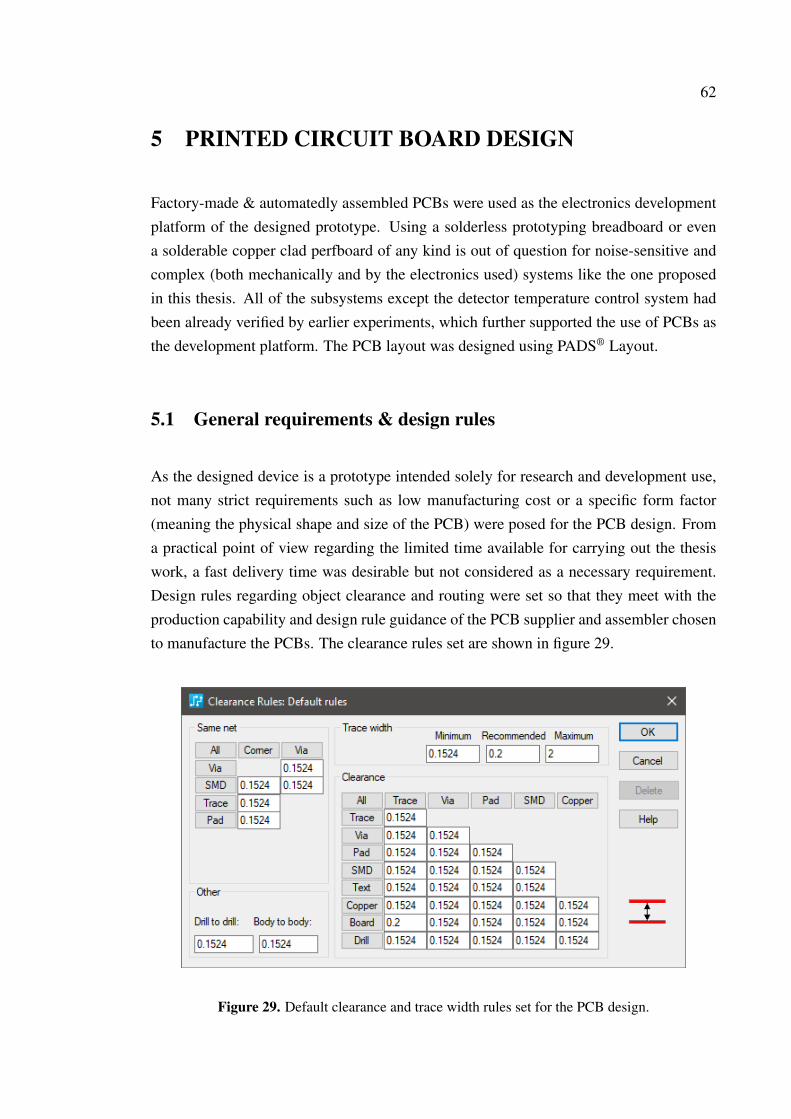
62
5 PRINTED CIRCUIT BOARD DESIGN
Factory-made & automatedly assembled PCBs were used as the electronics developmentplatform of the designed prototype. Using a solderless prototyping breadboard or evena solderable copper clad perfboard of any kind is out of question for noise-sensitive andcomplex (both mechanically and by the electronics used) systems like the one proposedin this thesis. All of the subsystems except the detector temperature control system hadbeen already verified by earlier experiments, which further supported the use of PCBs asthe development platform. The PCB layout was designed using PADS® Layout.
5.1 General requirements & design rules
As the designed device is a prototype intended solely for research and development use,not many strict requirements such as low manufacturing cost or a specific form factor(meaning the physical shape and size of the PCB) were posed for the PCB design. Froma practical point of view regarding the limited time available for carrying out the thesiswork, a fast delivery time was desirable but not considered as a necessary requirement.Design rules regarding object clearance and routing were set so that they meet with theproduction capability and design rule guidance of the PCB supplier and assembler chosento manufacture the PCBs. The clearance rules set are shown in figure 29.
Figure 29. Default clearance and trace width rules set for the PCB design.

63
The optical cuvette used created the only few mechanical requirements for the PCBs.These included both the location and orientation of the IR source and detector compo-nents, as well as the location of the mounting holes used to attach the circuit board to theoptical cuvette using screws. The source and detector components had to be mounted onthe bottom side of the PCB, which would be the side facing towards the optical cuvette.The board outline is rectangular by shape and has rounded corners for comfortable han-dling. The top side projection of the PCB is 80 x 120 mm by size. It will be possible togreatly reduce the size of the PCB in possible future versions - this is because once theprototype has been found to function as desired, more components can be placed on thebottom side of the PCB.
5.2 Layer setup & interconnections
A total of four signal layers were deployed, since increasing the number of layers dras-tically simplifies the manual routing process and helps in minimizing current loop area.Having multiple layers with ground and power planes also provides better protection forelectromagnetic interference due to the image plane effect [98]. Open plated-through holevias with a drill diameter of 0.4 mm and a plate width of 0.2 mm were used for the in-terconnections between the layers of the PCB. The vias were intentionally left non-tentedto promote testability, and to enable minor modifications to be made if such would beneeded. Thermal vias were placed under the MCU (4.6) and TEC controller (4.5) foradditional heat removal. Thicknesses of the different layers are listed in table 4.
Table 4. Build-up of the PCBs.
Name Type Thickness (µm)
Solder mask Coating N/D
Top Component 35
Prepreg Substrate 110
Layer 2 Plane 35
Prepreg Substrate 1200
Layer 3 Plane 35
Prepreg Substrate 110
Bottom Component 35
Solder mask Coating N/D
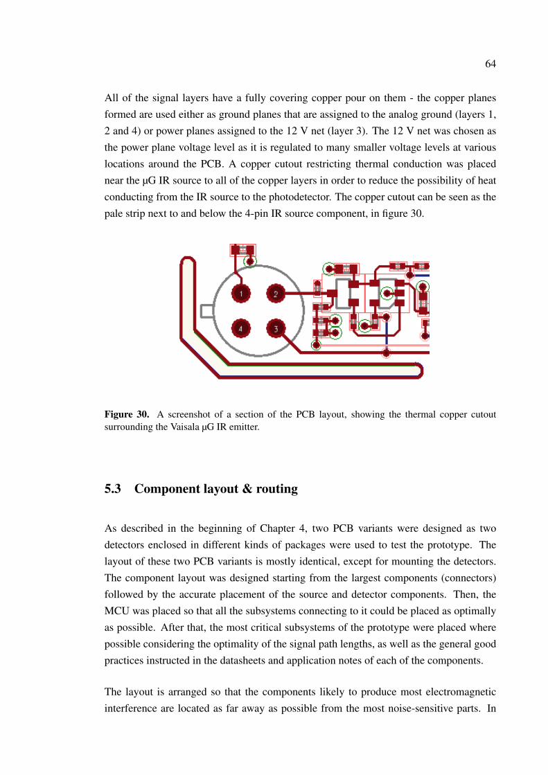
64
All of the signal layers have a fully covering copper pour on them - the copper planesformed are used either as ground planes that are assigned to the analog ground (layers 1,2 and 4) or power planes assigned to the 12 V net (layer 3). The 12 V net was chosen asthe power plane voltage level as it is regulated to many smaller voltage levels at variouslocations around the PCB. A copper cutout restricting thermal conduction was placednear the µG IR source to all of the copper layers in order to reduce the possibility of heatconducting from the IR source to the photodetector. The copper cutout can be seen as thepale strip next to and below the 4-pin IR source component, in figure 30.
Figure 30. A screenshot of a section of the PCB layout, showing the thermal copper cutoutsurrounding the Vaisala µG IR emitter.
5.3 Component layout & routing
As described in the beginning of Chapter 4, two PCB variants were designed as twodetectors enclosed in different kinds of packages were used to test the prototype. Thelayout of these two PCB variants is mostly identical, except for mounting the detectors.The component layout was designed starting from the largest components (connectors)followed by the accurate placement of the source and detector components. Then, theMCU was placed so that all the subsystems connecting to it could be placed as optimallyas possible. After that, the most critical subsystems of the prototype were placed wherepossible considering the optimality of the signal path lengths, as well as the general goodpractices instructed in the datasheets and application notes of each of the components.
The layout is arranged so that the components likely to produce most electromagneticinterference are located as far away as possible from the most noise-sensitive parts. In
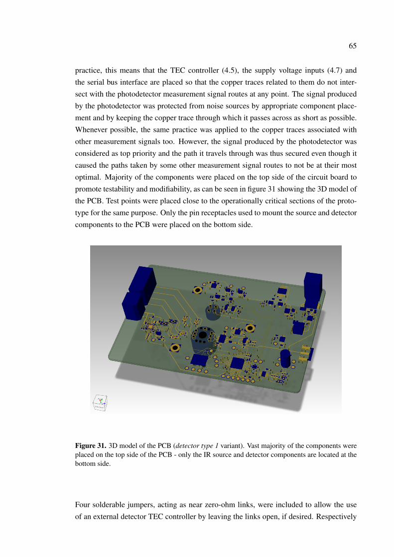
65
practice, this means that the TEC controller (4.5), the supply voltage inputs (4.7) andthe serial bus interface are placed so that the copper traces related to them do not inter-sect with the photodetector measurement signal routes at any point. The signal producedby the photodetector was protected from noise sources by appropriate component place-ment and by keeping the copper trace through which it passes across as short as possible.Whenever possible, the same practice was applied to the copper traces associated withother measurement signals too. However, the signal produced by the photodetector wasconsidered as top priority and the path it travels through was thus secured even though itcaused the paths taken by some other measurement signal routes to not be at their mostoptimal. Majority of the components were placed on the top side of the circuit board topromote testability and modifiability, as can be seen in figure 31 showing the 3D model ofthe PCB. Test points were placed close to the operationally critical sections of the proto-type for the same purpose. Only the pin receptacles used to mount the source and detectorcomponents to the PCB were placed on the bottom side.
Figure 31. 3D model of the PCB (detector type 1 variant). Vast majority of the components wereplaced on the top side of the PCB - only the IR source and detector components are located at thebottom side.
Four solderable jumpers, acting as near zero-ohm links, were included to allow the useof an external detector TEC controller by leaving the links open, if desired. Respectively

66
closing the links utilizes the temperature control circuit integrated onboard the PCB. Thejumpers can be seen in figure 31 above the mounting hole closest to the bottom edgeof the image. Solderable jumpers were chosen instead of zero-ohm resistors, becausewhen operated with maximum voltage and current, the power consumed by the TECcan theoretically reach over 600 mW. If zero-ohm resistors would have been used, theirpackage would have had to be quite large because of the theoretical maximum power theywould have to withstand. In addition, solderable jumpers are easier to operate with; theycan be closed by adding a sufficient amount of solder and opened using desoldering braid.
5.4 Automated error checking
The design was first inspected thoroughly by visually reviewing each of the subsystemsand traces in order to detect any clearly visible design faults. Lastly, the automated de-sign rule check feature of PADS®, called Verify Design (figure 32), was used to makedefinitively sure that no clearance or connectivity related design errors exist in the layout.
Figure 32. A screenshot showing the dialog box of the Verify Design feature of PADS® Layout.
Both of the automated error checks performed returned a clean **NO ERRORS FOUND**
notification, meaning that the PCB layouts had been designed as intended in their electri-cal circuit diagrams.

67
6 EVALUATING OPERATION OF THE PROTOTYPE
In this chapter, the measurement setups used to test the functionality of the prototype, aswell as the results obtained, are introduced. Successfulness of the electronics and PCBdesign is considered by comparing the measurement results to the design calculations andsimulation-based estimations & expectations, where applicable. Finally, proposals forfuture work and further research are given.
6.1 Description of experiments
A total of five experiments were conducted for the prototype within the framework of thisthesis in order to ensure desired operation of each of the designed subsystems included:
• Experiment A – basic operation of the prototype: First, to ensure that the PCBsdo not contain significant manufacturing defects or major design faults, supply volt-age was connected alternately to the two different inputs available, and the TECdriver supply voltage input separate from the other two inputs. Voltages of all thetest points and regulator outputs were measured.
• Experiment B – µG IR source control electronics: it was first verified that asufficient amount of power is supplied to the µG IR source by measuring the voltageover it. In addition, the power supplied to the IR source was manually changed,proving that the µG operating voltage control electronics work as intended.
• Experiment C – FPI filter control electronics: the FPI filter control electronicswere tested by setting different output values for the related PWM control signals.By measuring, it was verified that the output voltages are of right amplitude, andthat the switch used to change between the two voltages operates nominally.
• Experiment D – photodetector signal amplification: the amplified baseline sig-nal level of both of the photodetector variants was measured to confirm that theamplifier setup works as it is supposed to.
• Experiment E – TEC driver: first, a small resistive load was used to simulate aTEC element in order to test that the voltage level and the amount of current flowingthrough the actual TEC would not exceed their set maximum limits. Then, thetemperature of an actual detector TEC was controlled in order to ensure operationof the designed control circuit and the digital control loop.

68
6.2 Measurement setups
All of the experiments described in section 6.1 were performed using the same basic mea-surement setup, seen in figure 33. The PCBs were attached to an optical cuvette, whichwas then enclosed inside an aluminum measurement chamber. A small part of the opticalcuvette can be seen as the black section between the PCB and the measurement cham-ber. In the measurements performed within the framework of this thesis, the chamber wasused to reduce the possible effects of ambient IR radiation and variation in the backgroundconcentration of the target gas in the laboratory premises. The two vertically aligned tubefitting mounting holes, seen at the side of the chamber, were blocked for the duration ofthe experiments.
Figure 33. A photograph showing the PCB attached to an optical cuvette enclosed inside a seal-able measurement chamber. The chamber can be used to perform measurements with knowngas concentrations, by attaching tube fittings to the two threaded holes visible on the side of thechamber.

69
During each experiment, the PCB was powered using a Vaisala 219690 USB cable. Thecable was connected to a laptop computer at one end, and to the threaded vertical 4-pinM8 male connector of the prototype (seen near the lower right corner of the PCB in figure33) at the other end. Experiment E required the use of an additional laboratory powersupply unit because of the current demand of the TEC element, described in more detailin section 4.7. The bench power supply unit used is a Keysight Technologies E36103A, aprogrammable DC power supply with a maximum output rating of 20 V, 2 A and 40 W.
Measurement data related to Experiments A, B, C & D was captured using a TektronixDPO3014 oscilloscope. The ground lead of the oscilloscope probe used was connected tothe PCB’s analog ground, which acts as the reference point for the electronics. Voltagesand waveforms of the different subsystems tested were then inspected one by one to meetthe objectives of Experiments A–D. Measurement data obtained from Experiment E wasacquired using a Fluke 179 True RMS Multimeter, and by logging thermistor temperaturedata on a personal computer via serial bus by operating the prototype using a command-line interface. The experiment was conducted by first simulating the integrated TECs ofthe detectors, using a set of power resistors. Three power resistors, with a nominal resis-tance of 1.3 Ω and maximum power dissipation of 25 W each, were connected in parallelto achieve a total resistance resembling that of a miniaturized Peltier element and havinga sufficient power dissipation capability. The resistor pack was connected to the outputof the TEC driver. For the duration of this experiment, the actual TEC element (insidethe detector package) was separated from the TEC driver output by leaving the solderablejumpers - included on the PCB for this purpose - in the open position. After desired ac-tion of the TEC driver had been confirmed, the solderable jumpers were closed and theintegrated TEC element of a photodetector was tested.
6.3 Results & discussion
Experiment A produced the results shown in table 5. All of the regulated and boostedvoltage levels were within an acceptable error range, and nothing of unexpected naturewas observed when voltages of the test points of the PCB were inspected one by one. Thevoltage levels shown in the Nominal [V] column of table 5 are the target values of thedifferent voltages needed for operating the prototype. The values shown in the Measured[V] column are averages of the measured voltage levels of three measurement iterations.After ensuring that the operating voltages of the PCB were nominal and before performingExperiments B–E, the embedded software developed for the prototype was flashed to theMCU using the RS-232 serial bus, allowing full control of the prototype’s features.
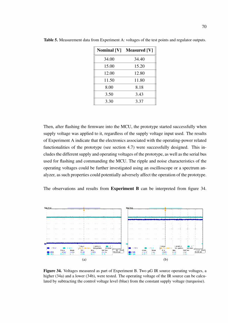
70
Table 5. Measurement data from Experiment A: voltages of the test points and regulator outputs.
Nominal [V] Measured [V]
34.00 34.40
15.00 15.20
12.00 12.80
11.50 11.80
8.00 8.18
3.50 3.43
3.30 3.37
Then, after flashing the firmware into the MCU, the prototype started successfully whensupply voltage was applied to it, regardless of the supply voltage input used. The resultsof Experiment A indicate that the electronics associated with the operating-power relatedfunctionalities of the prototype (see section 4.7) were successfully designed. This in-cludes the different supply and operating voltages of the prototype, as well as the serial busused for flashing and commanding the MCU. The ripple and noise characteristics of theoperating voltages could be further investigated using an oscilloscope or a spectrum an-alyzer, as such properties could potentially adversely affect the operation of the prototype.
The observations and results from Experiment B can be interpreted from figure 34.
(a) (b)
Figure 34. Voltages measured as part of Experiment B. Two µG IR source operating voltages, ahigher (34a) and a lower (34b), were tested. The operating voltage of the IR source can be calcu-lated by subtracting the control voltage level (blue) from the constant supply voltage (turquoise).

71
Subfigures 34a & 34b show the measured potential difference over the µG IR emitter,using two different control signal voltages. In both of the subfigures, the turquoise voltagesignal is the IR source’s constant supply voltage of 8.25 V, and the blue voltage signal isthe software-selectable control signal voltage that defines the actual operating voltage ofthe IR emitter as the potential difference between the constant supply voltage and thecontrol signal voltage. Subfigure 34a shows a larger operating voltage of 7.8 V appliedover the emitter, whereas subfigure 34b shows a smaller operating voltage of 0.72 V.As the constant supply voltage of 8.25 V remained stable and the control signal voltagecould be set as desired, Experiment B essentially proved that the control electronics forthe IR source (see section 4.2) work as intended. The control electronics allow the userof the prototype to either manually set different operating voltages for the IR source, orto modulate the operating voltage of the IR source using a software-based control loop.In practice, the IR source can be modulated by switching the control voltage between ahigher and a lower voltage at a desired frequency using a digital control loop.
Experiment C produced the measurement results shown in figure 35.
(a) (b)
Figure 35. Two oscilloscope screen captures obtained as part of Experiment C, showing that boththe High and Low operating voltages of the FPI filter can be manually set.
The FPI filter’s operating voltage was measured using a single oscilloscope probe placedat the positive input terminal lead of the FPI filter. The ON voltage was initially set to15.9 V and the OFF voltage close to 0 V, seen as the measured High and Low voltagelevels in figure 35a. The ON and OFF voltages were then changed, one after the other, sothat the ON voltage was reduced and OFF voltage was increased. Figure 35b shows theoperating voltage waveform after both of the changes had been made. It was thus shownthat the voltages can be individually set to desired values, corresponding to the pass-bandwavelengths of interest, within the supply voltage range of the FPI filter. Essentially,

72
Experiment C demonstrated that it is possible to set two different supply voltages, inde-pendent of each other, for the FPI filter incorporated in the prototype’s optical path.
Before performing Experiment D, a small modification had to be made to all of thePCBs. The reason was, that on preliminary tests it was found out that the waveform of theamplified photodetector measurement signal was not quite as it was expected to be. Theamplification circuit worked in principle, as the signal was indeed amplified to a measur-able voltage level, but the signal was not square-wave shaped as it should have been, ascan be seen in figure 36. Various alternative possible causes were examined, includingthe possibility of amplifier bias voltage swing, and the possibility of too weak a 1st stageamplifier gain. However, these options could not explain the problem. Finally, detailedAC-analysis simulation of the amplifier setup revealed the most plausible explanation.
Figure 36. An oscilloscope screen capture showing the overshoot problem related to the photode-tector measurement signal amplification setup, detected prior to performing Experiment D.
The apparent cause for this undesired behavior was the phase shift created by the com-bination of the DC-decoupling capacitor C11 and the 2nd stage amplifier’s input resistorR38 (see figure 18 for reference), which caused the system to be unstable over the mea-surement frequency range. The problem was fixed by choosing a higher resistance valuefor the 2nd stage amplifier’s input resistor R38, effectively decreasing the reactive part ofthe series impedance and significantly reducing the phase shift of the series impedancefrom about -35° to approximately -0.34° at the frequency of 100 Hz. Alternatively, ca-pacitor C11 could have been replaced, but a capacitor of sufficiently high capacitance in asuitably sized component package was not available at short notice. After modifying thePCBs, Experiment D could be carried out. The amplified signal of both of the photodetec-tors (presented in sections 4.3.1 & 4.3.2) expectedly appeared as a square wave waveform,

73
as shown in figures 37 and 38. The amplified photodetector measurement signals wereobtained operating at two different modulation frequencies. Both of the measurementswere performed using the oscilloscope in AC coupling mode to remove the 1.25 V DCoffset off the signal, as well as to maximize the oscilloscope’s resolution.
(a) (b)
Figure 37. The amplified measurement signal of the Hamamatsu photodetector (4.3.2) with mod-ulation frequencies of 100 (a) & 150 (b) Hz.
As can be seen by comparing figures 37a & 37b, the modulation frequency was success-fully changed by commanding the MCU. Based on the measurements, the amplified peak-to-peak voltage of the Hamamatsu detector appears to vary around 800 mV depending onthe background concentration of the target gas. Some noise can be seen in the amplifiedresponse of the photodetector, though it is not possible to determine the exact quantity orsource of it on the basis of the measurements made. The possible noise sources, such asvariation of the target gas concentration within the prototype’s optical path, are uncertainby their significance. Figure 38 shows the amplified signal of the VIGO detector.
(a) (b)
Figure 38. The amplified measurement signal of the VIGO photodetector (4.3.1) with modulationfrequencies of 100 (a) & 150 (b) Hz.

74
Again, the modulation frequencies of 100 & 150 Hz were used, as seen in figures 38a &38b. The peak-to-peak voltage of the VIGO detector was about the same as that of theHamamatsu detector’s, being approximately 800 mV by average. However, the SNR ofthe amplified signal produced by the VIGO photodetector seemed to be much smaller.This should be mostly due to the larger difference in size between the active area of theVIGO detector and the emitter area of the IR source used – the detector’s active area isonly about 1% of the size of the IR source’s emitter area. This grand difference in sizeleads to only a very small portion of the IR radiation to be collected by the photodetector,making noise a dominant part of the measurement signal. Experiment D showed that notall the necessary aspects were initially taken into account when designing the amplifiersetup for the photodetector measurement signal. After finding out the likely root cause ofthe stability-related issue and modifying the component values, the amplifier setup couldbe, however, fixed to work as originally intended. The difference between the responsesof the two different photodetectors tested was significant. This difference in performancewould presumably narrow substantially, if the active areas of the detectors would be equalin size. The measured peak-to-peak voltage of both of the photodetectors tested stillleaves some margin for raising the gain of either the 1st or the 2nd amplifier stage, as theinput range of the ADC is 0.0–2.5 V and the photodetector signal has an offset of +1.25 V.
First part of Experiment E was performed using a set of power resistors and a multi-meter, as described in section 6.2. By commanding the MCU, the control signal voltagefed to the ADN8833 TEC controller was manually set to first correspond to the maximumpossible voltage across the TEC element, and then to the minimum voltage over the TEC(being desirably as close to 0 V as possible). The voltage over the power resistor packand the current flowing through it were then measured. The maximum voltage was mea-sured to be 0.887 V and the maximum current, respectively, 635 mA. This would suggestthat the voltage and current limits set for the quantities in section 4.5.1 work as designed.In addition to the maximum values, applying the OFF-state control signal voltage wastested. When the control signal voltage was set to the OFF state, the voltage measuredover the power resistor pack was 0.001 V and the current flowing through it 0.001 A, re-spectively. The polarity of the voltage was correct within the control signal voltage rangecorresponding to the experimentally observed TEC voltage range limits of 0 to 0.887 V,meaning that also the direction of the current flow would be correct and the TEC ele-ment would operate in cooling mode. After the limits of magnitude of the TEC voltageand current, as well as the polarity of the voltage and the direction of current flow hadbeen experimentally found to be proper, the second part of Experiment E was carried out.
The second part of Experiment E (figures 39 & 40) was done using the digital proportional–

75
integral temperature control loop implemented in the embedded software. The tempera-ture of the Hamamatsu detector’s integrated TEC element was adjusted to three differ-ent temperature set points: +20, 0 and -30 °C. The experiment was conducted in theroom temperature of about +27 °C, meaning that the theoretical ΔTMAX of the TECelement (see section 4.3.2) could not have precluded the experiment. With the propor-tional and integral terms chosen, the system’s response showed no noticeable oscilla-tion during settling. Correspondingly, the settling time of the system was quite slowdepending on the set point temperature chosen. The higher the ΔT, the longer the sys-tem’s settling time. The settling times for the different temperature set points were ap-proximately 2 minutes for 20 °C, 3 minutes for 0 °C and 6 minutes for -30 °C. Oncethe temperature set point had been reached, the temperature remained close to the setpoint value. After stabilizing to the set point, the temperature varied within an errorrange of ≤ ±0.05 °C. This level of accuracy should be sufficient in the application.
Figure 39. The Hamamatsu photodetector’s integrated TEC was cooled down to three temperatureset points (+20, 0 & -30 °C) to ensure desired operation of the TEC driver.
In addition to acquiring the temperature data, the photodetector measurement signal wasmeasured once the temperature set points had been reached, in order to find out how

76
operating the TEC controller affects the signal. The effect of operating the TEC con-troller can be seen in figure 40. On preliminary assessment, it quite clearly appeared thatthe amount of noise in the photodetector measurement signal increased when the TECcontroller was used to control the temperature of the photodetector. The phenomenoncan be most clearly noticed by comparing the measured waveforms of figures 37a & 40.
Figure 40. An oscilloscope screen capture showing an increase in the amount of noise presentin the amplified photodetector measurement signal, when the TEC controller was being used forcooling the photodetector.
The main findings of Experiment E can be summarized as follows. The TEC driver andthe associated electronics work as designed, making it possible to set and control the tem-perature of the integrated TEC element of the photodetectors tested. However, as usingthe TEC driver seems to produce a considerable amount of noise to the photodetector’ssignal, the desired benefit of cooling the detector was not achieved. The cause of thisadverse effect needs to be identified among the other topics of further research.
6.4 Future work
From a purely performance-centric point of view, it can be stated with great certaintythat the design could be further optimized by making component choices based not on
77
established practices and availability, but instead on the factors that most significantlyaffect the operation of the prototype. For the most part the component choices were madereasonably, but in some respects this situation was not fully achieved due to problemsin component availability. From the point of view of possible future productization ofthe concept, the matter is slightly different, however. Considering productization, thedesign should be further unified, which in this context would mean reducing the number ofdifferent components used to a minimum, as well as choosing less expensive componentsof sufficient quality. In addition, it would likely be a good idea to evaluate the possibilityof using only typical passive component values that are generally available (meaningcomponent values included in some of the commonly used E series of preferred numbers)to reduce the possibility of production-related availability problems – however this shouldpreferably not be done at the expense of performance.
The photodetector measurement signal amplifier setup design should be once more eval-uated in detail and optimized, and then, if it turns out to be necessary, the use of otherpossible amplification implementations could be considered. In addition to the amplifiersetup, the TEC control circuit requires further evaluation. The proportional and integralterms of the digital control loop could be further optimized using the heuristic Ziegler–Nichols method, or similar. Then, the performance of the TEC controller (4.5) shouldbe benchmarked in chosen temperature set points using the Thorlabs TED200C (brieflymentioned in section 1.2 and seen within the block diagram in figure 13) as a reference.The exact cause of the noise observed in the photodetector measurement signal, relatedto the TEC control circuit, should be investigated and thoroughly understood so that theamount of noise caused by the temperature control electronics can be reduced by imple-menting appropriate design changes. If it is decided that the use of the TEC controller iscontinued after optimizing the associated circuit, tests in different temperatures, humidi-ties and other controlled environmental conditions should be performed to see whetherthe TEC controller performance is sufficient in changing environments and the gas sensorperformance remains good. On the other hand, if no clear solution to the noise problemis found, the use of other PCB-attached alternatives for implementing the temperaturecontrol functionality could be considered. After these steps of further research have beenexecuted, the prototype’s performance should be defined by measuring known concen-trations of the target gas and defining the signal-to-noise ratio of the measurement signalproduced by the photodetector. This should eventually make it possible to estimate theaccuracy, precision and resolution of the sensor. Taking these steps of future work shouldallow defining the need for changes in the electronics and PCB design in order to reachthe desired level of performance.

78
7 CONCLUSION
The aim of this master’s thesis was to combine previously created separate prototype de-signs and functionalities proven to work, related to the development of a novel opticalgas sensor. For this purpose, a single-circuit-board prototype, that could be easily usedfor testing the performance of the concept, was designed and implemented. As a novelfeature, electronics required to control the temperature of a TEC integrated inside a pho-todetector were designed. For future reference, it should be noted that considerable care isrequired when designing multi-stage amplifier setups. In particular, impedance loads witha significantly high reactive component do affect the operation of operational amplifiers -a phenomenon that could have been detected earlier on than it was by accurate and moreversatile simulation and by having a closer look at the related theory. Perhaps the singlemost significant highlight related to the design work done is the TEC controller integratedon the PCB. Designing and testing this kind of an integrated solution for controlling thedetector’s temperature has significant novelty value within the framework of the ongoingresearch & development work related to the topic of this thesis.
In addition to the design work done, early stage tests were performed as part of of this the-sis in order to confirm basic operation of each of the subsystems incorporated in the pro-totype. The experiments performed were delimited to ensuring that the prototype worksas designed and desired. Based on the experiments performed for the prototype, the ob-jectives set for the work were all achieved. The IR emitter as well as the voltage-tunableFPI filter could be controlled appropriately and the measurement signal produced by thephotodetector was succesfully amplified to an adequate voltage range. Tests performedwith the integrated TEC controller provided promising results, however optimizing andevaluating performance of the design should be continued. Most of the functionalitiesworked as intended right away, however some of them required minor changes to bemade, mainly limited to modifying individual component values. It should be noted thatsuch need of modifying the design is an expected, inherent and normal part of any kindof prototyping. The main results of this master’s thesis are the prototype electronics andPCB designed. The electronics and PCB designed are an essential part of an optical gassensor prototype that allows easily testing a rapid-measurement concept by measuringknown concentrations of the target gas. Altogether, the implemented prototype managedto meet the fundamental criteria and requirements set for its operation. Once the follow-up actions proposed in section 6.4 have been made, the prototype and the informationobtained by testing and using it should allow evaluating the concept’s feasibility morecomprehensively than was previously possible.
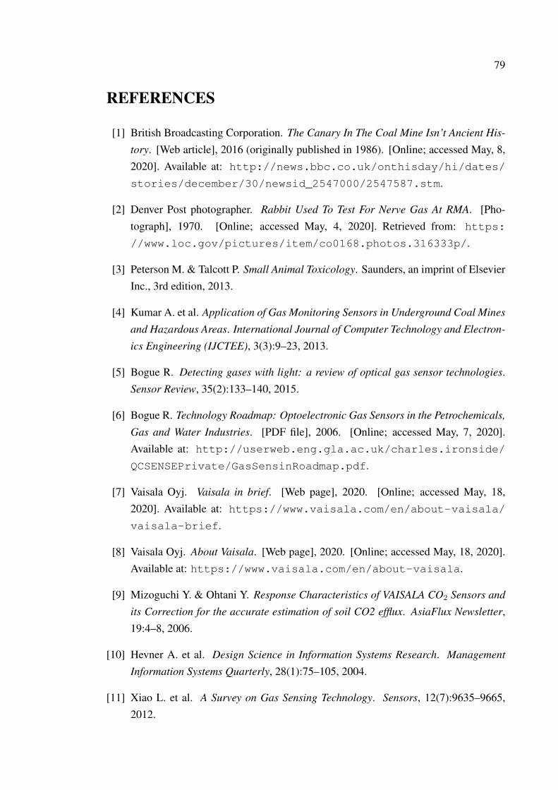
79
REFERENCES
[1] British Broadcasting Corporation. The Canary In The Coal Mine Isn’t Ancient His-
tory. [Web article], 2016 (originally published in 1986). [Online; accessed May, 8,2020]. Available at: http://news.bbc.co.uk/onthisday/hi/dates/
stories/december/30/newsid_2547000/2547587.stm.
[2] Denver Post photographer. Rabbit Used To Test For Nerve Gas At RMA. [Pho-tograph], 1970. [Online; accessed May, 4, 2020]. Retrieved from: https:
//www.loc.gov/pictures/item/co0168.photos.316333p/.
[3] Peterson M. & Talcott P. Small Animal Toxicology. Saunders, an imprint of ElsevierInc., 3rd edition, 2013.
[4] Kumar A. et al. Application of Gas Monitoring Sensors in Underground Coal Mines
and Hazardous Areas. International Journal of Computer Technology and Electron-
ics Engineering (IJCTEE), 3(3):9–23, 2013.
[5] Bogue R. Detecting gases with light: a review of optical gas sensor technologies.Sensor Review, 35(2):133–140, 2015.
[6] Bogue R. Technology Roadmap: Optoelectronic Gas Sensors in the Petrochemicals,
Gas and Water Industries. [PDF file], 2006. [Online; accessed May, 7, 2020].Available at: http://userweb.eng.gla.ac.uk/charles.ironside/
QCSENSEPrivate/GasSensinRoadmap.pdf.
[7] Vaisala Oyj. Vaisala in brief. [Web page], 2020. [Online; accessed May, 18,2020]. Available at: https://www.vaisala.com/en/about-vaisala/
vaisala-brief.
[8] Vaisala Oyj. About Vaisala. [Web page], 2020. [Online; accessed May, 18, 2020].Available at: https://www.vaisala.com/en/about-vaisala.
[9] Mizoguchi Y. & Ohtani Y. Response Characteristics of VAISALA CO2 Sensors and
its Correction for the accurate estimation of soil CO2 efflux. AsiaFlux Newsletter,19:4–8, 2006.
[10] Hevner A. et al. Design Science in Information Systems Research. Management
Information Systems Quarterly, 28(1):75–105, 2004.
[11] Xiao L. et al. A Survey on Gas Sensing Technology. Sensors, 12(7):9635–9665,2012.
80
[12] Mehta A. Introduction to the Electromagnetic Spectrum and Spectroscopy.[Web article], 2011. [Online; accessed May, 19, 2020]. Available at:https://pharmaxchange.info/2011/08/introduction-to-
the-electromagnetic-spectrum-and-spectroscopy/.
[13] Kumar P. & Mina U. Fundamentals and Techniques of Biophysics and Molecular
Biology. Pathfinder Publication, New Delhi, India, 2nd edition, 2016.
[14] The Editors of Encyclopædia Britannica. Wave-particle duality. [Web article]published by Encyclopædia Britannica, inc., 2016. [Online; accessed May, 24,2020]. Available at: https://www.britannica.com/science/wave-
particle-duality.
[15] Ronan P. EM spectrum. [Picture], 2007. [Online; accessed May, 11, 2020].Retrieved and adapted from: https://commons.wikimedia.org/wiki/
File:EM_spectrum.svg under the CC BY-SA 3.0 license.
[16] Baggott J. Beyond Measure: Modern Physics, Philosophy and the Meaning of Quan-
tum Theory. Oxford University Press, 2nd edition, 2003.
[17] Byrnes J. Unexploded Ordnance Detection and Mitigation. Springer Sci-ence+Business Media B.V., 1st edition, 2008.
[18] Prange A. & Modrow H. X-ray absorption spectroscopy and its application in bio-
logical, agricultural and environmental research. Reviews in Environmental Science
and Bio/Technology, 1:259–276, 2002.
[19] Savin S. et al. The applications of X-ray absorption spectroscopy in the study of
nanocrystalline materials and electrochemical systems. Comptes Rendus Chimie,11(9):948–963, 2008.
[20] Shouyuan T. et al. Applications and techniques of microwave spectroscopy.Progress in Chemistry, 21:1060–1069, 2009.
[21] Wlodarczak G. Microwave and Radiowave Spectroscopy, Applications. In Ency-
clopedia of Spectroscopy and Spectrometry. Academic Press, an imprint of ElsevierInc., 2017.
[22] Dinh T.-V. et al. A review on non-dispersive infrared gas sensors: Improvement
of sensor detection limit and interference correction. Sensors and Actuators B:
Chemical, 231:529–538, 2016.
[23] Popa D. & Udrea F. Towards Integrated Mid-Infrared Gas Sensors. Sensors,19(9):2076, 2019.

81
[24] Coates J. Interpretation of Infrared Spectra, A Practical Approach. In Encyclopedia
of Analytical Chemistry (eds R.A. Meyers and M.L. McKelvy). John Wiley & SonsLtd., 2006.
[25] Asahi H. & Horikoshi Y. Molecular Beam Epitaxy: Materials and Applications for
Electronics and Optoelectronics. John Wiley & Sons Ltd., 2019.
[26] MIRO Analytical AG. High-precision Multicompound Gas Analyzer. [Webpage]. [Online; accessed June, 15, 2020]. Available at: https://www.miro-analytical.com/Product.html.
[27] Thermo Nicolet Corp. TN-00128 – FT-IR vs. Dispersive Infrared. [ApplicationNote], 2002. [Online; accessed June, 01, 2020]. Available at: http://www.
thermo.com.cn/Resources/200802/productPDF_21615.pdf.
[28] Vaisala Oyj. Carbocap Sensor Illustration. [Picture], 2018. [Material Bank ofVaisala Oyj; accessed May, 11, 2020].
[29] Anderson R. & Wong J. Non-Dispersive Infrared Gas Measurement. InternationalFrequency Sensor Association (IFSA) Publishing, S.L., 1st edition, 2012.
[30] Walters C. et al. The Spectrophotometric Analysis and Modeling of Sunscreens.Journal of Chemical Education, 74(1):99, 1997.
[31] Haigh M. et al. Mid-infrared AlxIn1−xSb light-emitting diodes. Applied Physics
Letters, 90(23):231116, 2007.
[32] Fanchenko S. et al. LED-based NDIR natural gas analyzer. IOP Conference Series:
Materials Science and Engineering, 108:012036, 2016.
[33] Asahi Kasei Microdevices Corp. AKM releases three products suitable for NDIR
flammable gas sensing: IR LED AK9703, IR sensor AK9730, and IR sensor
AFE IC AK9723. [Web article], 2020. [Online; accessed May, 25, 2020].Available at: https://www.akm.com/eu/en/about-us/news/2020/
20200213-ak9703ak9730ak9723/.
[34] IBSG Co. Ltd. LIGHT-EMITTING DIODE LED-430 - NS. [Datasheet], 2013.[Online; accessed May, 25, 2020]. Available at: http://www.ibsg-st-
petersburg.com/datasheet/LED/LED-430-NS.pdf.
[35] Scholz L. et al. MID-IR LED-based, photoacoustic CO2 sensor. In Procedia Engi-
neering Vol. 120, EUROSENSORS 2015, pages 1233–1236. Elsevier Ltd., 2015.

82
[36] Johnston S. Gas monitors employing infrared LEDs. Measurement Science and
Technology, 3(2):191–195, 1992.
[37] Fanchenko S. et al. Multi-wavelength IR method for monitoring air pollution in
cities. In 2016 IEEE International Smart Cities Conference (ISC2), pages 1–6, 2016.
[38] Rumyantsev S. et al. Low frequency noise and long-term stability of noncoherent
light sources. Journal of Applied Physics, 96(2):966–969, 2004.
[39] Hodgkinson J. et al. Non-dispersive infra-red (NDIR) measurement of carbon diox-
ide at 4.2µm in a compact and optically efficient sensor. Sensors and Actuators B:
Chemical, 186:580–588, 2013.
[40] Sato K. et al. Comparative effectiveness of light emitting diodes (LEDs) and Lasers
in near infrared photoimmunotherapy. Oncotarget, 7(12):14324–14335, 2016.
[41] Fujitsuka N. et al. Alcohol Detection in Exhaled Air by NDIR Method. IEEJ Trans-
actions on Sensors and Micromachines, 132(7):219–223, 2012.
[42] Mueller G. Electroluminescence I, volume 64 of Semiconductors and Semimetals.Academic Press, an imprint of Elsevier Inc., 1999.
[43] Uotila J. Comparison of infrared sources for a differential photoacoustic gas detec-
tion system. Infrared Physics & Technology, 51:122–130, 2007.
[44] Hodges M. & Schiessl U. Lead salt tunable diode lasers: key devices for high-
sensitivity gas analysis. In Proc. SPIE 3628, In-Plane Semiconductor Lasers III,1999.
[45] Razeghi M. et al. Quantum cascade lasers: from tool to product. Optics Express,23(7):8462–8475, 2015.
[46] Normand E. & Howieson I. Quantum-cascade lasers enable gas-sensing technol-
ogy. Laser Focus World, 43(4):90–92, 2007.
[47] Electro Optical Components Inc. Laser Gas Detection Using Tunable Diode Laser
Spectrometry (TDLS). [Product catalogue], 2020. [Online; accessed May, 29,2020]. Available at: https://www.eoc-inc.com/lasers-ndir-gas-
detection/.
[48] Sch; a user of Wikipedia. Black-body spectrum for temperatures between 300 K
and 10,000 K in a log-log diagram. [Picture], 2006. [Online; accessed June,1, 2020.]. Retrieved from: https://commons.wikimedia.org/wiki/
File:BlackbodySpectrum_loglog_150dpi_en.png under the CC BY-SA 3.0 license.
83
[49] Oshino Lamps Ltd. What is NDIR? [Web page]. [Online; accessed June,03, 2020]. Available at: https://www.oshinolamps.co.jp/en/ndir/
nondispersive-infrared/.
[50] CMOS IR GmbH. Homepage of CMOS IR Gmbh. [Web page]. [Online; accessedJune, 02, 2020]. Available at: https://www.cmosir.com/.
[51] Micro-Hybrid Electronic GmbH. Homepage of Micro-Hybrid Electronic GmbH.[Web page]. [Online; accessed June, 02, 2020]. Available at: https://www.
microhybrid.com/en/.
[52] Hawkeye Technologies Inc. Homepage of Hawkeye Technologies, Inc. [Webpage]. [Online; accessed June, 02, 2020]. Available at: http://www.
hawkeyetechnologies.com/.
[53] Axetris AG. Homepage of Axetris AG, a company of the Leister Group. [Web page].[Online; accessed June, 02, 2020]. Available at: https://www.axetris.com/en.
[54] Alluxa Inc. Alluxa Learning Center – What are thin-film optical filters? [Web page].[Online; accessed June, 04, 2020]. Available at: https://www.alluxa.com/learning-center/what-are-thin-film-optical-filters/.
[55] Honsberg C. & Bowden S. Anti-Reflection Coatings. [Web page]. [Online; accessedJune, 03, 2020]. Available at: https://www.pveducation.org/pvcdrom/design-of-silicon-cells/anti-reflection-coatings.
[56] Paschotta R. (RP Photonics Consulting GmbH). RP Photonics Encyclopedia. [Webpage]. [Online; accessed June, 02, 2020]. Available at: https://www.rp-
photonics.com/encyclopedia.html.
[57] Vaisala Oyj. B211311EN-A – Infrared Sensor Technology and its Impact on HVAC
CO2 Measurement Accuracy. [Application Note], 2013. [Online; accessed June,03, 2020]. Available at: https://www.vaisala.com/sites/default/
files/documents/CEN-TIA-HVAC-CO2-Measurement-Accuracy-
B211311EN-A.pdf.
[58] Rogalski A. Infrared Detectors. LLC, CRC Press, 2nd edition, 2010.
[59] Ready J. Optical Detectors and Human Vision, volume TT79 of Fundamentals of
Photonics edited by Roychoudhuri, C. The International Society for Optics andPhotonics (SPIE), 2008.

84
[60] Bass M. et al. Handbook of Optics, volume 1. Inc., McGraw-Hill, 2nd edition, 1995.
[61] Stiens J. et. al. Infrared Thermo-Electric Photodetectors. In F. Duarte, editor, Laser
Pulse Phenomena and Applications, chapter 8. IntechOpen, 2010.
[62] Piotrowski J. & Rogalski A. Uncooled long wavelength infrared photon detectors.Infrared Physics & Technology, 46:115–131, 2004.
[63] Zamboni J. Integrated thermoelectric cooler/package for infrared detector array
temperature stabilization. In Proceedings Vol. 5209, Materials for Infrared Detec-
tors III, page 173. The International Society for Optics and Photonics (SPIE), 2003.
[64] Zoran J. Micro and Nanophotonics for Semiconductor Infrared Detectors. SpringerInternational Publishing, 1st edition, 2014.
[65] Huuhtanen M. Optimal Mid-Infrared Photon Detectors for Use with Voltage-
Tunable Filters in Gas Sensing Applications. Master’s thesis, Aalto University,School of Electrical Engineering, Finland, 2018.
[66] Zumbahlen H., editor. Linear Circuit Design Handbook. Newnes, an imprint ofElsevier Inc., 1st edition, 2008.
[67] Razavi B. The Transimpedance Amplifier [A Circuit for All Seasons]. IEEE Solid-
State Circuits Magazine, 11(1):10–97, 2019.
[68] Lee P. of Analog Devices Inc. AN-940 – Low Noise Amplifier Selection Guide for
Optimal Noise Performance. [Application Note], 2013. [Online; accessed June, 08,2020]. Available at: https://www.analog.com/media/en/technical-documentation/application-notes/AN-940.pdf.
[69] Schweber B. How to Choose and Use Precision Op Amps Effec-
tively. [Web article], 2019. [Online; accessed June, 08, 2020]. Avail-able at: https://www.digikey.com/en/articles/how-to-choose-and-use-precision-op-amps-effectively.
[70] Williams J. of Linear Technology Corp. Application Note 21 – Compos-
ite Amplifiers. [Application Note], 1986. [Online; accessed June, 08,2020]. Available at: https://www.analog.com/media/en/technical-documentation/application-notes/an21f.pdf.
[71] Teare S., editor. Practical Electronics for Optical Design and Engineering. TheInternational Society for Optics and Photonics (SPIE), 1st edition, 2016.

85
[72] Hamamatsu Photonics K.K. Technical Information SD-12 – Characteristics and
use of infrared detectors. [Application Note], 2011. [Online; accessed May, 22,2020]. Available at: https://www.hamamatsu.com/resources/pdf/
ssd/infrared_kird9001e.pdf.
[73] Maxim Integrated Products Inc. AN6139 – Selecting the Right ADC for
Your Application. [Application Note], 2015. [Online; accessed June, 08,2020]. Available at: https://www.maximintegrated.com/en/design/technical-documents/tutorials/6/6139.html.
[74] Pelgrom M. Analog-to-Digital Conversion. Springer Science+Business Media LLC,2nd edition, 2013.
[75] Giovino B. IoT Microcontrollers Have ADCs, but Know When to Choose and
Apply an External ADC. [Web article], 2018. [Online; accessed June, 09,2020]. Available at: https://www.digikey.com/en/articles/iot-
microcontrollers-have-adcs-know-when-apply-an-external-
adc.
[76] Maxim Integrated Products Inc. AN748 – The ABCs of Analog to Digital Converters:
How ADC Errors Affect System Performance. [Application Note], 2002. [Online;accessed June, 09, 2020]. Available at: https://www.maximintegrated.
com/en/design/technical-documents/tutorials/7/748.html.
[77] Rohm Co. Ltd. Electronics Basics – What is a DC/DC converter? [Webtutorial]. [Online; accessed June, 09, 2020]. Available at: https://www.
rohm.com/electronics-basics/dc-dc-converters/linear-vs-
switching-regulators.
[78] Ebermann M. et al. I3.1 - Design, Operation and Performance of a Fabry-Perot-Based MWIR Microspectrometer. In Proceedings OPTO 2009 & IRS2 2009, pages233–238. AMA Association for Sensors and Measurement, 2009.
[79] Drebushchak V. The Peltier Effect. Journal of Thermal Analysis and Calorimetry,91(1):311–315, 2008.
[80] Weremczuk J. et al. Flexible coplanar line of low heat load to cooled infrared
detector. In Procedia Engineering Vol. 120, EUROSENSORS 2015, pages 1183–1186. Elsevier Ltd., 2015.
[81] TEC Microsystems GmbH. Thermoelectric Coolers Intro. [Web tutorial]. [Online;accessed June, 09, 2020]. Available at: https://www.tec-microsystems.com/faq/thermoelectic-coolers-intro.html.
86
[82] Vishay Dale Electronics Inc. Document Number 33016 – NTC and PTC Thermis-
tors. [Application Note], 2002. [Online; accessed June, 09, 2020]. Available at:https://www.vishay.com/docs/33016/engnote.pdf.
[83] Prodic A. & Maksimovic D. Digital PWM controller and current estimator for a
low-power switching converter. In COMPEL 2000. 7th Workshop on Computers in
Power Electronics. Proceedings (Cat. No.00TH8535), pages 123–128, 2000.
[84] Computer Language Company Inc. Definition: control signal. [Web article]published by Computer Language Company Inc. [Online; accessed June, 10,2020]. Available at: https://www.computerlanguage.com/results.
php?definition=control+signal.
[85] Thakor M. et al. Precise temperature control through Thermoelectric Cooler with
PID controller. In 2015 International Conference on Communications and Signal
Processing (ICCSP), pages 1118–1122, 2015.
[86] de Miguel S. et al. Identification model and PI and PID controller design for a novel
electric air heater. Automatika, 58(1):55–68, 2017.
[87] IEC 60115-8:2009. Fixed resistors for use in electronic equipment. Part 8: Sectional
specification - Fixed surface mount resistors. Geneve: International ElectrotechnicalCommission, 2009. 84 p.
[88] VIGO System S.A. MCT Photovoltaic detectors – PVI-2TE. [Datasheet], 2017.[Online; accessed June, 13, 2020]. Available at: https://vigo.com.pl/
produkty/pvi-2te/.
[89] Hamamatsu Photonics K.K. InAsSb photovoltaic detectors – P13243 se-
ries. [Datasheet], 2020. [Online; accessed June, 13, 2020]. Available at:https://www.hamamatsu.com/resources/pdf/ssd/p13243_
series_kird1130e.pdf.
[90] Analog Devices Inc. LTC2057/LTC2057HV – High Voltage, Low Noise Zero-
Drift Operational Amplifier. [Datasheet], 2013. [Online; accessed June, 14,2020]. Available at: https://www.analog.com/media/en/technical-documentation/data-sheets/2057f.pdf.
[91] Texas Instruments Inc. SLAA926A – Transimpedance amplifier circuit with
MSP430TM smart analog combo. [Application Note], 2020. [Online; accessedJune, 14, 2020]. Available at: https://www.ti.com/lit/an/slaa926a/slaa926a.pdf?ts=1592117224012.

87
[92] Analog Devices Inc. ADN8833 – Ultracompact, 1 A Thermoelectric Cooler (TEC)
Driver for Digital Control Systems, Rev. B. [Datasheet], 2018. [Online; accessedApr, 15, 2020]. Available at: https://www.analog.com/en/products/adn8833.html.
[93] VIGO System S.A. IR detectors user’s guide. [Application Note], 2018. [On-line; accessed May, 22, 2020]. Available at: https://vigo.com.pl/wp-
content/uploads/2018/07/IR_detectors_users_guide.pdf.
[94] Texas Instruments Inc. SNOAA12 – Methods to Reduce Thermistor Lineariza-
tion Error, Memory, and Power Requirements Over Wide Operating Temperature
Ranges. [Application Note], 2018. [Online; accessed June, 14, 2020]. Avail-able at: https://www.ti.com/lit/an/snoaa12/snoaa12.pdf?ts=
1592143688264.
[95] Texas Instruments Inc. SLOA024B – Analysis of the Sallen–Key Architecture. [Ap-plication Note], 2002. [Online; accessed June, 23, 2020]. Available at: https://www.ti.com/lit/an/sloa024b/sloa024b.pdf.
[96] Sinha P., editor. Speech Processing in Embedded Systems. Springer US, 2009.
[97] Texas Instruments Inc. LP295x-N Series of Adjustable Micropower Voltage Regula-
tors. [Datasheet], 2017. [Online; accessed May, 22, 2020]. Available at: https://www.ti.com/store/ti/en/p/product/?p=LP2951ACMM-3.3/NOPB.
[98] Carter B. & Mancini R. Op Amps for Everyone, 5th Edition. Newnes, an imprint ofElsevier Inc., 2017.

Appendix 1. MCU Pin Configuration
Pin # Function Schematic ID Additional notes
1 VREF- AGND Analog ground reference point for the +2.5 V internal reference voltage OUTPUT
2 VREF+ VREF_2V5 Internal +2.5 V reference voltage OUTPUT from the MCU to the detector amplifier interface
3 A2 VREF_TEC_2V5 Measure the TEC driver's internal 2V5 reference, divided to 1.25 V by a resistor voltage divider
4 A12 DET_MEAS Amplified measurement signal from the photodetector, DC offset +1.25 V
5 A13 I_TEC_MEAS Voltage proportional to the current flowing through the thermoelectric cooler (from ADN8833)
6 A14 V_TEC_MEAS Voltage over the thermoelectric cooler (from ADN8833)
7 A15 30V_MEAS FPI driver circuit supply voltage
8 P4.7 TEC_ENABLE ADN8833 TEC driver is enabled, when EN/SY input > 2.1 V and VLIM/SD input > 0.07 V
9 - TP2 -
10 TB0.1 IR_PWM Microglow IR source control voltage
11 TB0.2 FPI_PWM_1 FPI operating voltage 1
12 TDO JTAG_TDO -
13 TDI JTAG_TDI -
14 TMS JTAG_TMS -
15 TCK JTAG_TCK -
16 A8 NTC_MEAS Voltage over the resistor linearizing the detector's NTC thermistor
17 A9 I_IR_MEAS Voltage corresponding the current flowing through the microglow IR source
18 A10 V_IR_MEAS Voltage over the microglow IR source
19 A11 12V_MEAS -
20 - TP6 -
21 - TP7 -
22 TEST TEST -
23 RST RST / 3.3V -
24 UCA0TXD TXD -
25 UCA0RXD RXD -
26 - TP5 -
27 - TP15 -
28 - TP26 -
29 - TP3 -
30 - TP4 -
31 TB0.3 FPI_PWM_2 FPI operating voltage 2
32 TB0.4 TEC_CTRL_PWM Control signal for the ADN8833 TEC driver
33 P4.4 LED Supply voltage for a red LED indicator
34 - TP28 -
35 - TP29 -
36 DVSS AGND -
37 DVCC 3.3V -
38 P2.7 FPI_SW_CTRL Control signal for the SPDT switch used to modulate between FPI_PWM_1 and FPI_PWM_2
39 UCA1STE RE -
40 UCA1CLK DE -
41 AVSS1 AGND -
42 HFXIN Z1 -
43 HFXOUT Z1 -
44 AVSS2 AGND
45 - TP9 -
46 - TP14 -
47 AVSS3 AGND -
48 AVCC 3.3V -
49 THERM_PAD AGND Exposed / Thermal pad, connected to AGND