Embed Size (px)
Citation preview

Insulated Gate Bipolar Transistors (IGBTs)
Zheng Yang(ERF 3017, email: [email protected])
ECE442 Power Semiconductor Devices and Integrated Circuits
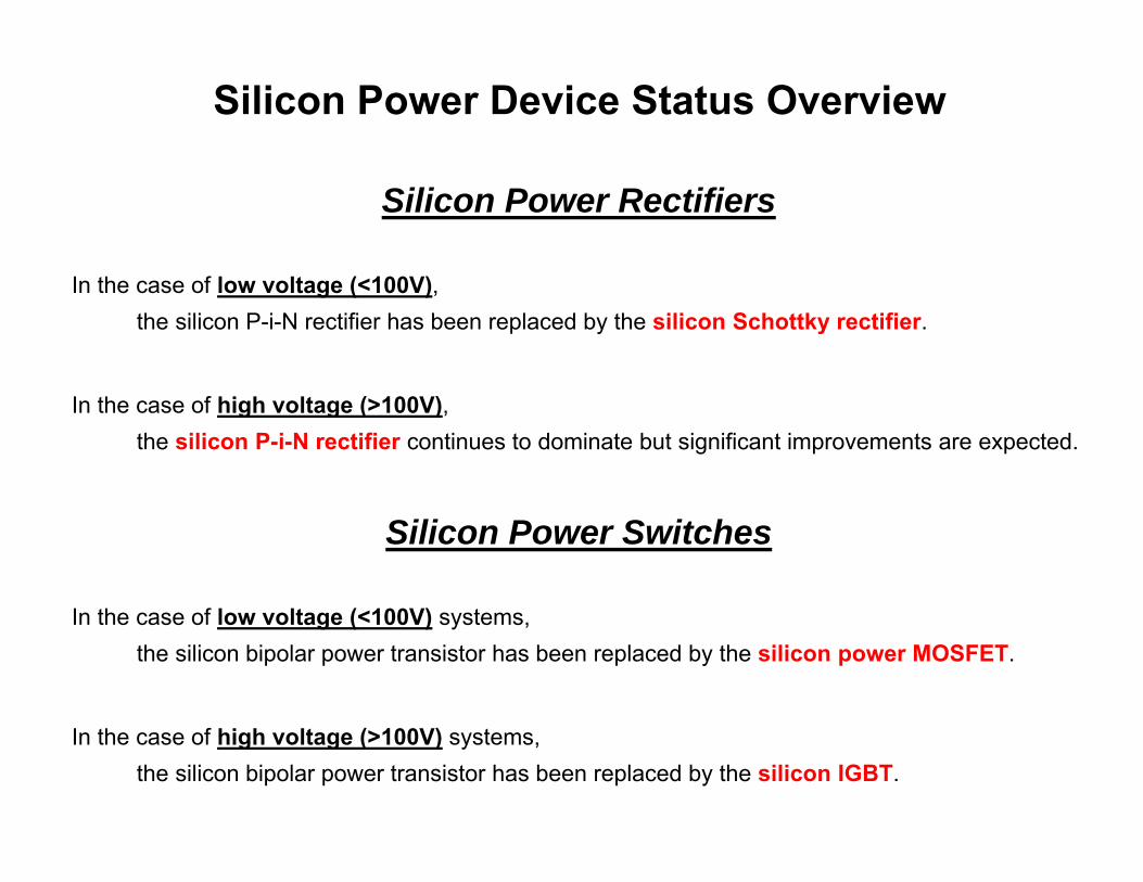
Silicon Power Device Status Overview
Silicon Power Rectifiers
In the case of low voltage (<100V),the silicon P-i-N rectifier has been replaced by the silicon Schottky rectifier.
In the case of high voltage (>100V),the silicon P-i-N rectifier continues to dominate but significant improvements are expected.
Silicon Power Switches
In the case of low voltage (<100V) systems,the silicon bipolar power transistor has been replaced by the silicon power MOSFET.
In the case of high voltage (>100V) systems,the silicon bipolar power transistor has been replaced by the silicon IGBT.
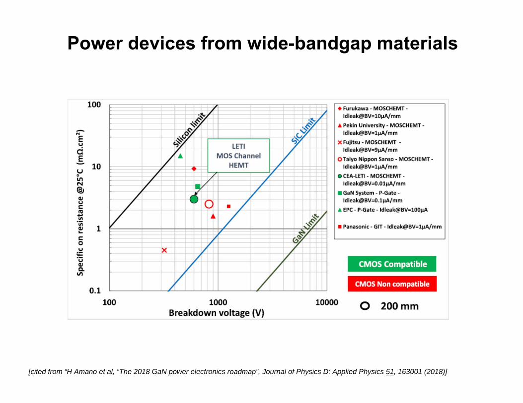
Power devices from wide-bandgap materials
[cited from “H Amano et al, “The 2018 GaN power electronics roadmap”, Journal of Physics D: Applied Physics 51, 163001 (2018)]
Background
Cons of power BJT: (1) One of the major shortcomings of the power BJT is its low-current gain when designed to operate at high voltages. (2) Poor SOA.
Pros of power BJT: Superior on-state characteristics.
Cons of power MOSFET: Due to its excellent electrical characteristics, it would be desirable to utilize power MOSFET’s for high voltage power electronics applications. Unfortunately, the specific on-resistance of the drift region increases very rapidly with increasing breakdown voltage because of the need to reduce its doping concentration and increase its thickness. Thus, in spite of the ability to obtain nearly ideal specific on-resistance with silicon UMOSFET structures (at relative low voltage), they are not satisfactory for applications that require breakdown voltages above 300 V due to their high on-state power dissipation.
Pros of power MOSFET: (1) It has an excellent low on-state voltage drop due to the low resistance of the drift region (at low and modest voltages). (2) It is a voltage-controlled device and has a very high input impedance in steady-state due to its MOS gate structure. (3) It has a very fast inherent switching speed in comparison to power BJTs, due to the absence of minority carrier injection. (4) It has superior ruggedness and forward biased safe operating area (SOA) when compared to power BJTs.
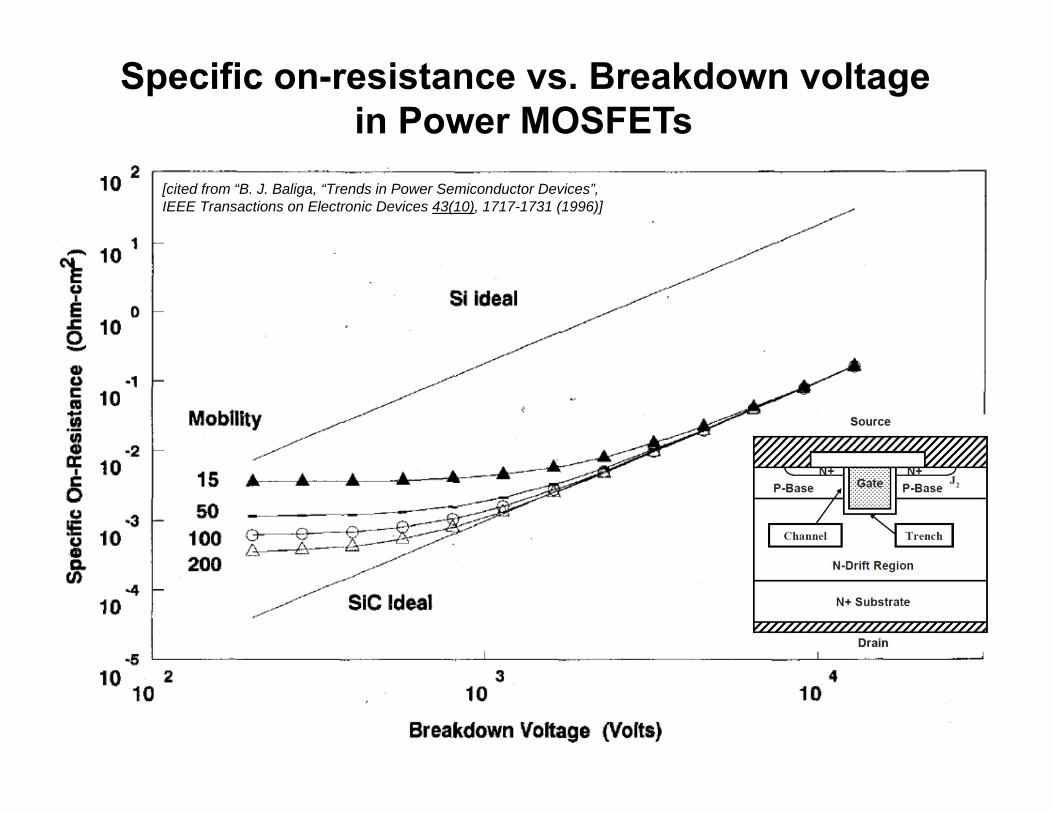
Specific on-resistance vs. Breakdown voltagein Power MOSFETs
[cited from “B. J. Baliga, “Trends in Power Semiconductor Devices”, IEEE Transactions on Electronic Devices 43(10), 1717-1731 (1996)]
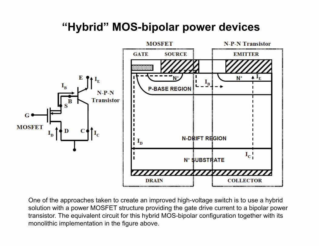
“Hybrid” MOS-bipolar power devices
One of the approaches taken to create an improved high-voltage switch is to use a hybrid solution with a power MOSFET structure providing the gate drive current to a bipolar power transistor. The equivalent circuit for this hybrid MOS-bipolar configuration together with its monolithic implementation in the figure above.
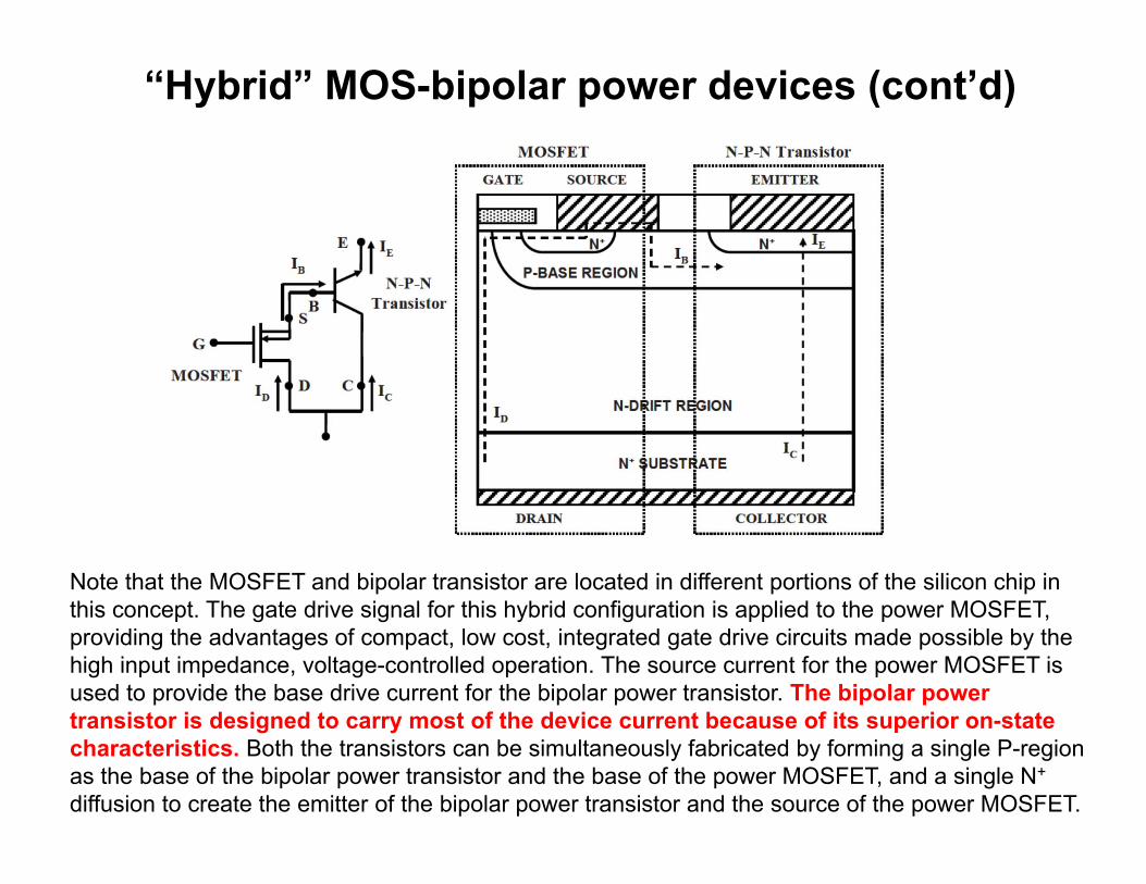
Note that the MOSFET and bipolar transistor are located in different portions of the silicon chip in this concept. The gate drive signal for this hybrid configuration is applied to the power MOSFET, providing the advantages of compact, low cost, integrated gate drive circuits made possible by the high input impedance, voltage-controlled operation. The source current for the power MOSFET is used to provide the base drive current for the bipolar power transistor. The bipolar power transistor is designed to carry most of the device current because of its superior on-state characteristics. Both the transistors can be simultaneously fabricated by forming a single P-region as the base of the bipolar power transistor and the base of the power MOSFET, and a single N+
diffusion to create the emitter of the bipolar power transistor and the source of the power MOSFET.
“Hybrid” MOS-bipolar power devices (cont’d)
“Hybrid” MOS-bipolar power devices (cont’d)
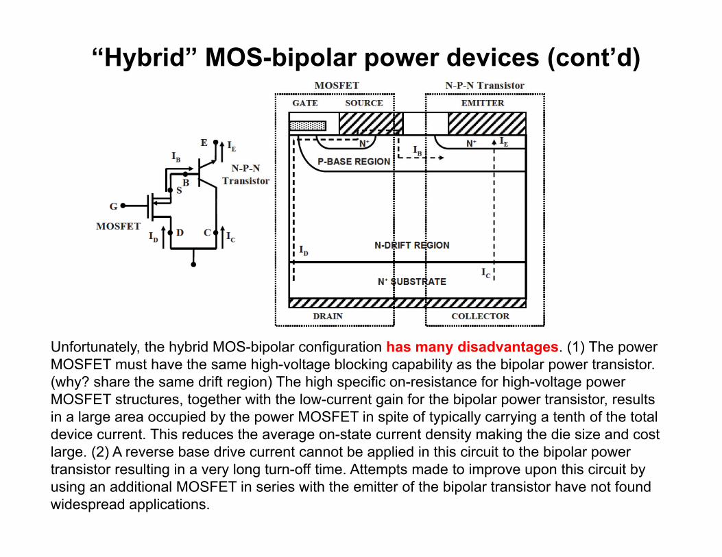
Unfortunately, the hybrid MOS-bipolar configuration has many disadvantages. (1) The power MOSFET must have the same high-voltage blocking capability as the bipolar power transistor. (why? share the same drift region) The high specific on-resistance for high-voltage power MOSFET structures, together with the low-current gain for the bipolar power transistor, results in a large area occupied by the power MOSFET in spite of typically carrying a tenth of the total device current. This reduces the average on-state current density making the die size and cost large. (2) A reverse base drive current cannot be applied in this circuit to the bipolar power transistor resulting in a very long turn-off time. Attempts made to improve upon this circuit by using an additional MOSFET in series with the emitter of the bipolar transistor have not found widespread applications.

Introduction of IGBTThe IGBT represents the true MOS-bipolar integration in the sense of intermingling the physics of operation of the MOSFET structure with the physics of operation of bipolar transistors. In thisconcept, the MOSFET structure is used to provide the base drive current for the bipolar transistor with the bipolar transistor used to modulate the conductivity of the drift region for the MOSFET structure. The reduced resistance of the power MOSFET structure allows providing much greater base drive current to the bipolar transistor in this configuration. Consequently, the bipolar power transistor structure can be altered from the traditional narrow-base N-P-N transistor structure to the wide-base P-N-P transistor structure. Although this change reduces the current gainof the bipolar transistor, it greatly enhances the SOA for the composite structure. Moreover, the IGBT structure has inherent forward- and reverse-blocking capability enabling its utilization in both DC and AC circuit applications.
The first IGBT devices with substantial current ratings were reported in the literature in 1982 with a symmetric (equal forward and reverse) blocking voltage capability of 600 V in recognition of their prospective applications in DC and AC circuits. It was soon apparent that the asymmetrical IGBT structure, with only forward-blocking capability, could be optimized with superior on-state and switching speed capability. The ability to scale the voltage rating of the IGBT structure with modest increase in the on-state voltage drop was also recognized immediately after its invention. This provided a strong impetus to scale up the voltage rating of IGBT structures.
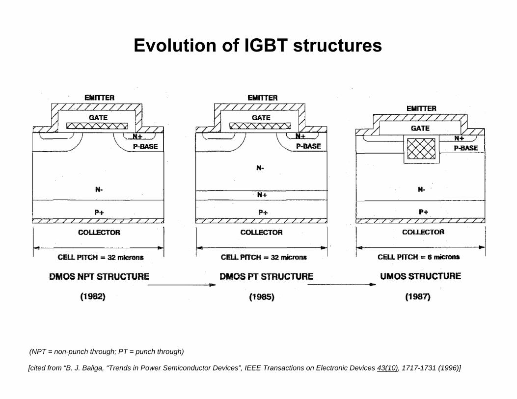
Interest in reducing the on-state voltage drop for IGBTs motivated the utilization of a trench-gate architecture in place of the planar-gate configuration in 1987. Subsequently, the observation of an enhanced carrier concentration in the vicinity of the trench-gate region, named the injection enhancement effect, has stimulated the development of devices that have the same high-voltage and current-handling capability as planar devices.
[cited from “B. J. Baliga, “Trends in Power Semiconductor Devices”, IEEE Transactions on Electronic Devices 43(10), 1717-1731 (1996)]
Evolution of IGBT structures
(NPT = non-punch through; PT = punch through)

Evolution of IGBT voltage ratings
The first IGBT devices with substantial current ratings were reported in the literature in 1982 with a symmetric (equal forward and reverse) blocking voltage capability of 600 V. Within a short span of 10 years, devices capable of supporting over 3,000 V were developed. Continued interest in using the IGBT for traction (electric locomotive drives) applications led to the scaling up of the voltage ratings to 6,500 V for these devices by work done in Europe and Japan.
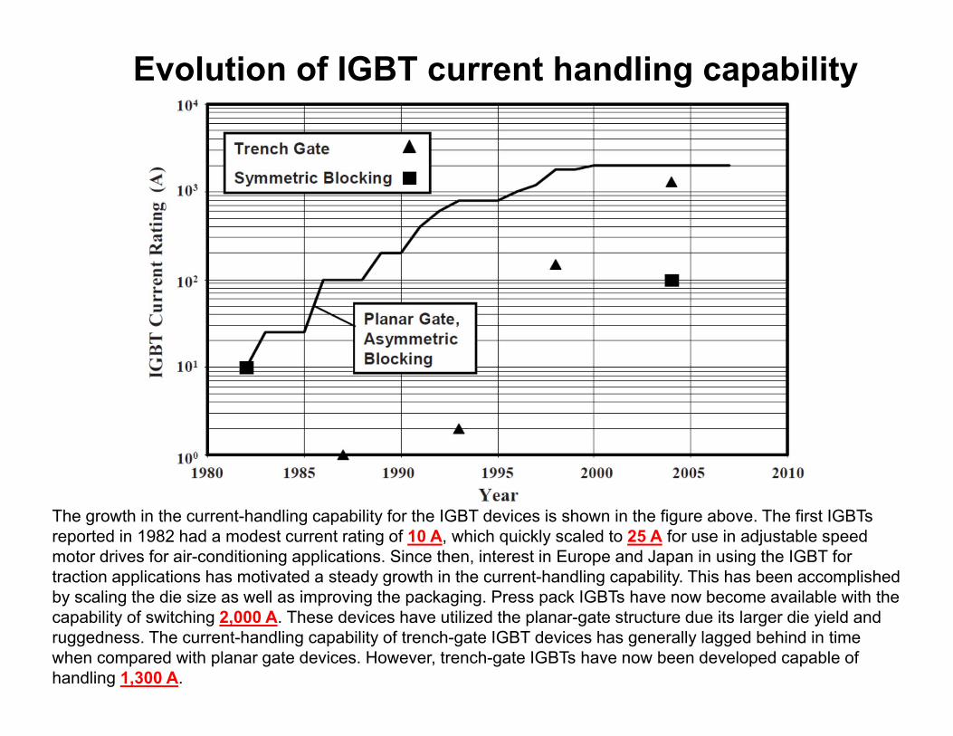
Evolution of IGBT current handling capability
The growth in the current-handling capability for the IGBT devices is shown in the figure above. The first IGBTs reported in 1982 had a modest current rating of 10 A, which quickly scaled to 25 A for use in adjustable speed motor drives for air-conditioning applications. Since then, interest in Europe and Japan in using the IGBT for traction applications has motivated a steady growth in the current-handling capability. This has been accomplished by scaling the die size as well as improving the packaging. Press pack IGBTs have now become available with the capability of switching 2,000 A. These devices have utilized the planar-gate structure due its larger die yield and ruggedness. The current-handling capability of trench-gate IGBT devices has generally lagged behind in time when compared with planar gate devices. However, trench-gate IGBTs have now been developed capable of handling 1,300 A.
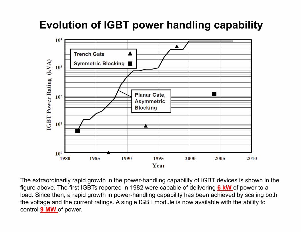
Evolution of IGBT power handling capability
The extraordinarily rapid growth in the power-handling capability of IGBT devices is shown in the figure above. The first IGBTs reported in 1982 were capable of delivering 6 kW of power to a load. Since then, a rapid growth in power-handling capability has been achieved by scaling both the voltage and the current ratings. A single IGBT module is now available with the ability to control 9 MW of power.
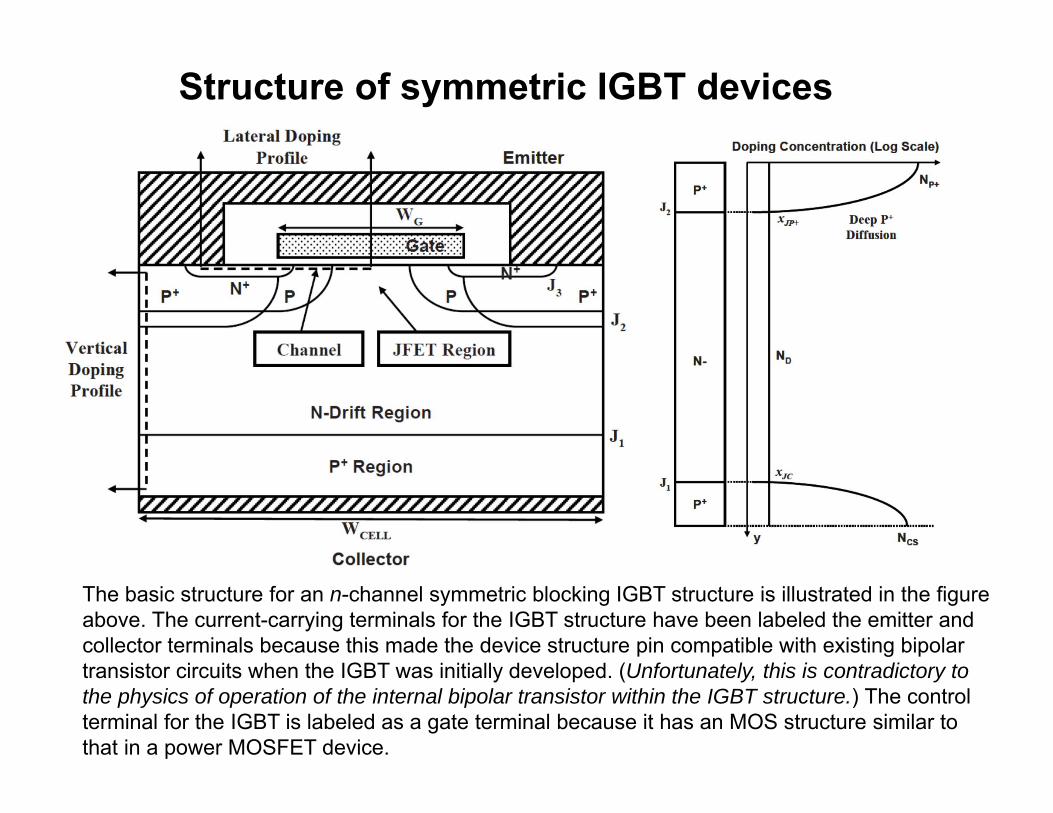
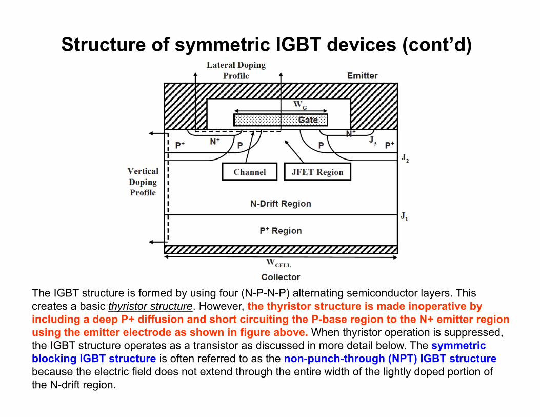
Structure of symmetric IGBT devices
The basic structure for an n-channel symmetric blocking IGBT structure is illustrated in the figure above. The current-carrying terminals for the IGBT structure have been labeled the emitter and collector terminals because this made the device structure pin compatible with existing bipolar transistor circuits when the IGBT was initially developed. (Unfortunately, this is contradictory to the physics of operation of the internal bipolar transistor within the IGBT structure.) The controlterminal for the IGBT is labeled as a gate terminal because it has an MOS structure similar to that in a power MOSFET device.
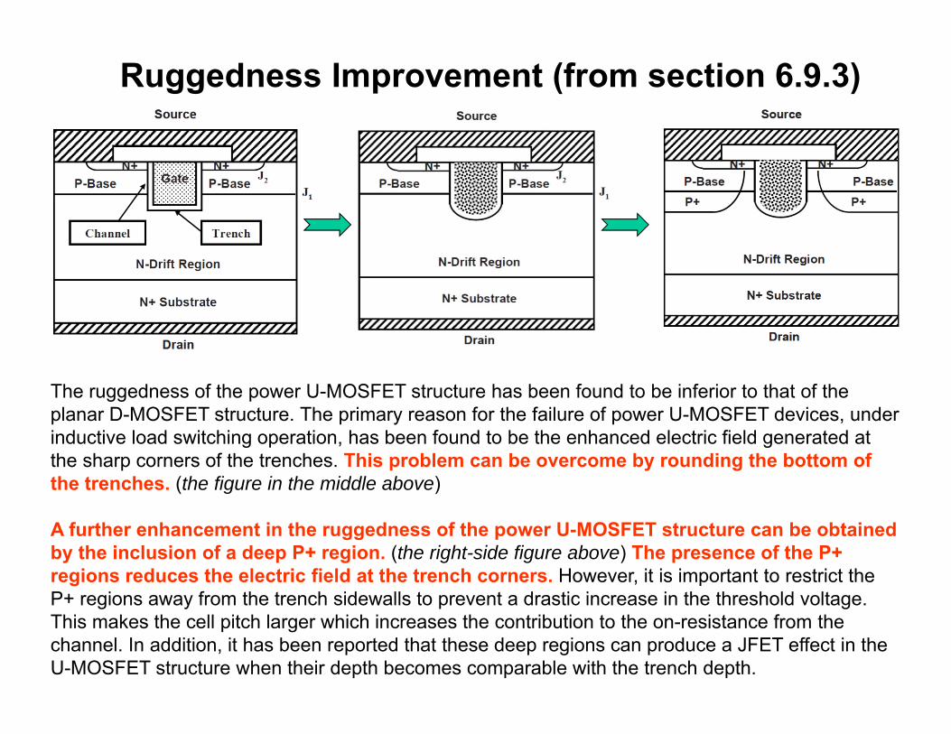
Ruggedness Improvement (from section 6.9.3)
The ruggedness of the power U-MOSFET structure has been found to be inferior to that of the planar D-MOSFET structure. The primary reason for the failure of power U-MOSFET devices, under inductive load switching operation, has been found to be the enhanced electric field generated at the sharp corners of the trenches. This problem can be overcome by rounding the bottom of the trenches. (the figure in the middle above)
A further enhancement in the ruggedness of the power U-MOSFET structure can be obtained by the inclusion of a deep P+ region. (the right-side figure above) The presence of the P+ regions reduces the electric field at the trench corners. However, it is important to restrict the P+ regions away from the trench sidewalls to prevent a drastic increase in the threshold voltage. This makes the cell pitch larger which increases the contribution to the on-resistance from the channel. In addition, it has been reported that these deep regions can produce a JFET effect in the U-MOSFET structure when their depth becomes comparable with the trench depth.
Structure of symmetric IGBT devices (cont’d)
The IGBT structure is formed by using four (N-P-N-P) alternating semiconductor layers. This creates a basic thyristor structure. However, the thyristor structure is made inoperative by including a deep P+ diffusion and short circuiting the P-base region to the N+ emitter region using the emitter electrode as shown in figure above. When thyristor operation is suppressed, the IGBT structure operates as a transistor as discussed in more detail below. The symmetric blocking IGBT structure is often referred to as the non-punch-through (NPT) IGBT structure because the electric field does not extend through the entire width of the lightly doped portion of the N-drift region.

Structure of asymmetric IGBT devices
The cross section for the asymmetric IGBT structure is shown in figure above. This IGBT structure is optimized for DC circuit applications where no reverse bias is applied to the device because it operates exclusively in the first quadrant of the i-v characteristics. The main distinguishing feature of the asymmetric IGBT structure is the introduction of an N-buffer layer within the N-drift region. This layer is sometimes referred to as the field-stop layer. In the asymmetric IGBT structure, the forward-blocking voltage can be supported by a thinner N-drift region resulting in reducing the on-state voltage drop. This structure is often referred to as the punch-through (PT) IGBT structure because the electric field “punches through” the entire lightly doped portion of the N-drift region.
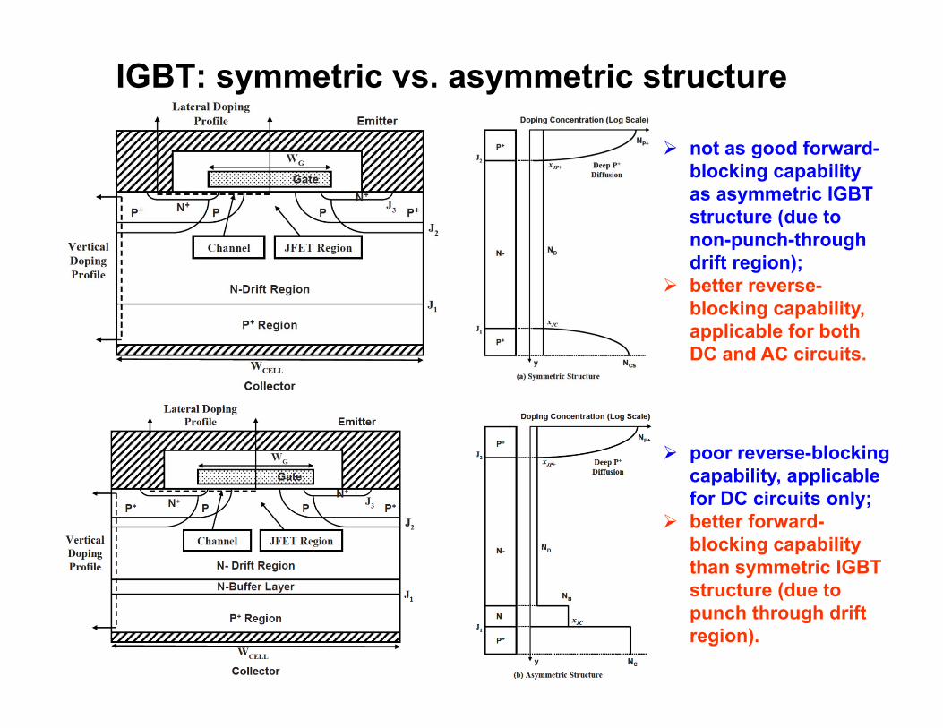
IGBT: symmetric vs. asymmetric structure
not as good forward-blocking capability as asymmetric IGBT structure (due to non-punch-through drift region);
better reverse-blocking capability, applicable for both DC and AC circuits.
poor reverse-blocking capability, applicable for DC circuits only;
better forward-blocking capability than symmetric IGBT structure (due to punch through drift region).
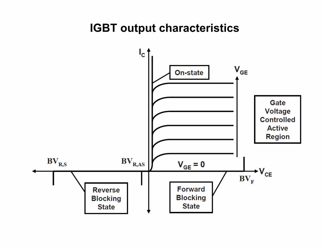
IGBT output characteristics

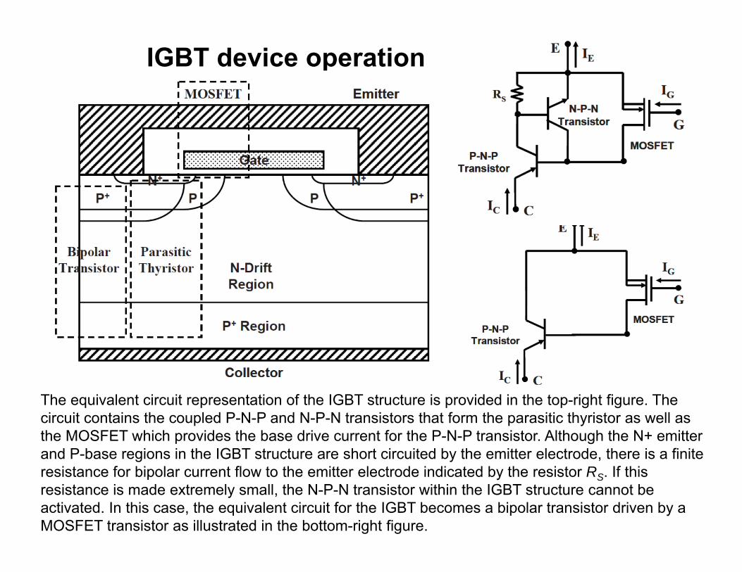
IGBT device operation
The IGBT structure consists of four alternating semiconductor layers that also constitute a thyristorstructure as indicated in figure above. It is necessary to completely suppress the operation of this thyristor structure to preserve the IGBT mode of operation over a broad range of currents and voltages. The suppression of the triggering and latch-up of the parasitic thyristor can be accomplished by numerous techniques. The successful implementation of these methods for suppressing the parasitic thyristor has been crucial to the success of the IGBT device as a productfor power electronic applications.
IGBT device operation
The equivalent circuit representation of the IGBT structure is provided in the top-right figure. The circuit contains the coupled P-N-P and N-P-N transistors that form the parasitic thyristor as well as the MOSFET which provides the base drive current for the P-N-P transistor. Although the N+ emitter and P-base regions in the IGBT structure are short circuited by the emitter electrode, there is a finiteresistance for bipolar current flow to the emitter electrode indicated by the resistor RS. If this resistance is made extremely small, the N-P-N transistor within the IGBT structure cannot be activated. In this case, the equivalent circuit for the IGBT becomes a bipolar transistor driven by a MOSFET transistor as illustrated in the bottom-right figure.

IGBT device operation (cont’d)The IGBT structure is capable of supporting high voltages when the gate electrode is short circuited to the emitter electrode by the external gate control circuit. When a positive bias is applied to the collector of either the symmetric or asymmetric IGBT structure, junction J1 is forward biased while junction J2becomes reverse biased. The applied voltage is supported across the reverse-biased deep P+/N-base (or N-drift) region junction J2 with the depletion region extending in the N-base region toward junction J1. The maximum forward-blocking voltage capability of the symmetric IGBT structure is determined by the open-base breakdown voltage of the P-N-P transistor. The thickness of the N-base region and the minority carrier lifetime in this region determine the breakdown voltage. In the case of the asymmetric IGBT structure, the lightly doped portion of the N-base (N-drift) region becomes completely depleted at a relatively low voltage. The electric field stops at the interface between the N-drift region and the N-buffer layer because of the relatively high doping concentration (1016-1017 cm−3) of the N-buffer layer. The N-buffer layer thickness and doping concentration must be sufficient to suppress reach-through and keep the gain of the P-N-P transistor as low as possible. In this case, the forward-blocking capability of the asymmetric IGBT structure will be determined by the thickness of the lightly doped portion of the N-base region.
When a negative bias is applied to the collector of the IGBT structure, junction J1 is reverse biased while junction J2 becomes forward biased. The applied voltage is supported across the reverse-biased junction J1 with the depletion region extending in the N-base region toward junction J2. The maximum reverse-blocking voltage capability of the symmetric IGBT structure is determined by the open-base breakdown voltage of the P-N-P transistor. The thickness of the N-base region and the minority carrier lifetime in this region determine the breakdown voltage. The reverse-blocking voltage capability is consequently equal to the forward blocking voltage capability. In the case of the asymmetric IGBT structure, the junction J1 cannot support a high voltage because of the high doping concentration (1016–1017 cm−3) of the N-buffer layer and the P+ collector region (1019 cm−3). This is acceptable for utilization of the asymmetric IGBT structure in DC circuits, especially for motor control where an antiparallel diode is connected across the IGBT device.
IGBT device operation (cont’d)The application of a positive bias to the gate of the IGBT structures creates an inversion layer channel under the gate electrode, which connects the N+ emitter region to the N-base region. This allows the transport of electron current from the N+ emitter region to the N-base region when a positive voltage is applied to the collector terminal. The electron current serves as the base drive current for the P-N-P transistor, promoting the injection of holes from the P+ collector/N-base junction J1. The injected holes produce the emitter current of the P-N-P bipolar transistor. Consequently, current flow occurs from the collector terminal to the emitter terminal with a bipolar component associated with the wide-base P-N-P transistor and a unipolar component via the channel of the MOSFET region. The N-base (N-drift) region of the IGBT structures operates with high-level injection conditions during current flow. This reduces the resistance of the N-base region allowing high-current flow with low on-state voltage drop. With sufficiently large gate bias to ensure operation of the MOSFET region in its linear (triode) mode, the on-state characteristics of the IGBT structure look like those of a P-i-N rectifier.
When the gate bias voltage is made only slightly above the threshold voltage of the MOSFET region, the channel enters pinch-off conditions resulting in limiting the electron current delivered to the N-base region. Since this limits the base drive current for the P-N-P bipolar transistor, its current also becomes saturated. The IGBT structure is therefore capable of exhibiting an active region with the collector current saturated at a value determined by the applied gate bias.
The switching of the IGBT device in power circuits can be performed by toggling the gate bias between zero and a positive bias VGS above its threshold voltage. When the gate bias is abruptly increased from zero to VGS, the collector current of the IGBT increases rapidly with an on-state voltage drop that is determined by the modulation of the conductivity of the N-base region. The rate of rise in collector current can be controlled by tailoring the rate of rise of the gate bias voltage. When the gate bias is rapidly decreased from VGS to zero, the collector current is turned off with a current tail associated with the removal of the stored charge in the N-base region. The turn-off switching losses can be reduced by decreasing the lifetime in the N-base region but this is accompanied by an increase in the on-state voltage drop. It is therefore customary to perform a tradeoff between the on-state voltage drop and the switching losses when designing IGBT devices.

24
SummaryThe IGBT was originally developed to replace the bipolar transistor in motor control applications. Immediately after the fabrication of the first prototypes, it was apparent that the superior on-state characteristics and simple gate drive requirements for the IGBT structure would greatly reduce the size and cost of the motor control system, making the device a viable candidate as a power switch. The replacement of bipolar power transistors by the IGBT devices was accomplished in a remarkably short time frame because the IGBT structure could be manufactured using the existing power MOSFET process.
It was initially conjectured that the IGBT structure would be limited to blocking voltages below 2,000 V. However, the optimization of the IGBT structure, together with the introduction of the trench-gate design, has made the device competitive at much higher voltages. Due to its attractive characteristics, the IGBT structure has been scaled to blocking voltages above 5,000 V. Due to its excellent overall performance, the IGBT structure is now the predominant power switch technology for applications that operate from power sources with voltages above 200 V. Until the advent of a cost-effective silicon carbide-based power switch technology1, the IGBT structure can be expected to be the dominant device for all medium and high power applications.
We discussed the basic device structures, operations, and equivalent circuit of IGBT in this chapter.
Sections discussed: 9.1, 9.2, 9.3 and 9.18Sections not discussed: 9.4-9.17
( 1 This book was published in 2008. Both SiC and GaN power devices have been developed fast and significantly since then.)