Embed Size (px)
Citation preview
DOE/NASA/0249-83/1 NASA-CR-168177
NASA-CR-168177 19840009005
Integral ~nvel1er/Battery Charger for Use in Electric Velhicles
David Thlmmesch Gould Inc Gould Research Center, Electronics Laboratory
September 1983
Prepared for National Aeronautics and Space Administration LewIs Research Center Under Contract DEN3-249
111111111111111111111111111111111111111111111 NF02600
for U.S. DEPARTMENT OF ENERGY Conservatifon and Renewable Energy Office 01 Vehicle and Engine R&D
i " I ~ 1Q0;1 I ' ..... } f ..... U t
LPNGLIC:Y RES[ARCH CENTEf( Llc"(/,RY, N.';SA
H~~' :TC:J, VIRG'rllA
https://ntrs.nasa.gov/search.jsp?R=19840009005 2018-07-15T15:36:40+00:00Z
DISCLAIMER
This report was prepared as an account of work sponsored by an agency of the United States Government Neither the United States Government nor any agency thereof, nor any of their employees, makes any warranty, express or Implied, or assumes any legal liability or responsibility for the accuracy, completeness, or usefulness of any information, apparatus, product, or process disclosed, or represents that ItS use would not infringe prIVately owned rights Reference herein to any specific commercial product, process, or service by trade name, trademark, manufacturer, or otherWise, does not necessarily constitute or Imply ItS endorsement, recommendation, or favoring by the United States Government or any agency thereof The views and opinions of authors expressed herein do not necessarily state or reflect those of the United States Government or any agency thereof
Printed In the United States of America
Available from National Technical Information Service U S Department of Commerce 5285 Port Royal Road Springfield, VA 22161
NTIS price codes1 Printed copy A07 Microfiche copy A01
1Codes are used for pricing all publications The code IS determined by the number of pages In the publication Information pertaining to the pricing codes can be found In the current Issues of the follOWing publications, which are generally available In most libraries Energy Research Abstracts (ERA), Government Reports Announcements and Index (GRA and I), SCIentifIc and Techntcal Abstract Reports (STAR), and publication, NTIS-PR-360 available from NTIS at the above address
DOElNASAl0249-83/1 NASA-CR-1681 n
Integral Inverter/Battery Charger for Use in Electric Vehicles
David Thimmesch Gould Inc. Gould Research Center, Electronics Laboratory
September 1983
Prepared for National Aeronautics and Space Administration Lewis Research Center Cleveland, Ohio 44135 Under Contract DEN3-249
for U.s. DEPARTMENT OF ENERGY Conservation and Renewable Energy Office of Vehicle and Engine R&D Washington, D.C. 20585 Under Interagency Agreement DE-AI01-77CS51044
#N1Y-/7tJ73
1.
2.
3.
4.
5.
6.
7.
8.
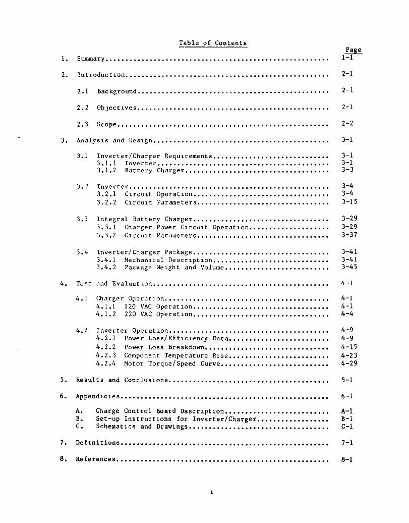
Table of Contents
Summary ........................................................ .
Introduc t lone ................•.........••..••..•.•••••.•.•••.••
2.1 Background ...•......•..•.........••.••••••.•••.••....•••.•
2.2 ObJect~ves ••••••••••••••••••••••••••••••••••••••••••••••••
2.3 Scope •••••••••••••••••••••••••••••••••••••••••••••••••••••
ArlalYS1S and Des1gn •.....•.....•.....•.•.••.•..••••.•••••••••••
3.1
3.2
3.3
3.4
Test
4.1
4.2
Inverter/Charrer Re q U 1 r erne n t s • • .. • • • ••••••••••••••••••••••• 3.1.1 3.1.2
Inverter ••••.•.•••••• Battery Charger .....•.••.••..••......•.••••••.•..••
Inverter ................. . 3.2.1 3.2.2
Clrcult Operatlon •• Clrcult Parameters •••
. ........... .
Charger ..........•.••••.... Integral Battery 3.3.1 Charger Power Clrcult Operat lone • 3.3.2 Clrcult Pardmeters •••••••••••••••
Inverter/ Charger Package ••••••••••••••••••••••••• 3.4.1 MechanIcal Descrlptlon.... • •••••• 3.4.2 Package WeIght and Volume. • ••••••
and EvaluatIon •••• ........................................ Operatlon •••••••••••••••• Charger
4.1.1 120 4.1.2 220
VAC Operatlon •••••• VAC OperatlOn.
Inverter Operat lon •••••••••••••••••• 4.2.1 Power Loss/Efflclency Data •••
. . . . . . . . . . . . . . . . . . . . . . 4.2.2 4.2.3 4.2.4
Power Loss Breakdown................ • ••••••• Component Temperature Rlse •••••••••••••••••••• Motor Torque/Speed Curve •••••••••••••••••••••••••••
Results and Conclus1ons ............•.......•.••..•.••••••••••••
Appendl.C1es ••••••••••••••••••••••••••••••••••••••••••••••••••••
A. B. C.
Charge Control Board Descrlptlon •••••••••••••••••••••••••• Set-up Instruct10ns for Inverter/Charger •••••••••••••••••• Schematlcs and Draw1ngs •••••••••••••••••••••••••••••••••••
De fl.ni t ions ••..•.••••.•••••••••••••.•••••••••••••••••••••••••••
References •.••••.•...•....•••••..••.•...••••••...•.•••••••••••.
1
Page 1-1
2-1
2-1
2-1
2-2
3-1
3-1 3-1 3-3
3-4 3-4 3-15
3-29 3-29 3-37
3-41 3-41 3-45
4-1
4-1 4-1 4-4
4-9 4-9 4-15 4-23 4-29
5-1
6-1
A-l B-1 C-l
7-1
8-1
3.1-1
3.2-1
3.2-2
3.2-3
3.2-4
3.2-5
3.2-6
3.2-7
3.2-8
3.2-9
3.2-10
3.2-11
3.2-12
3.2-13
3.2-14
3.3-1
3.3-2
3.3-3
3.3-4
3.3-5
3.3-6
3.4-1
3.4-2
4.1-1
4.1-2
4.1-3
4.1-4
4.1-5
4.1-6
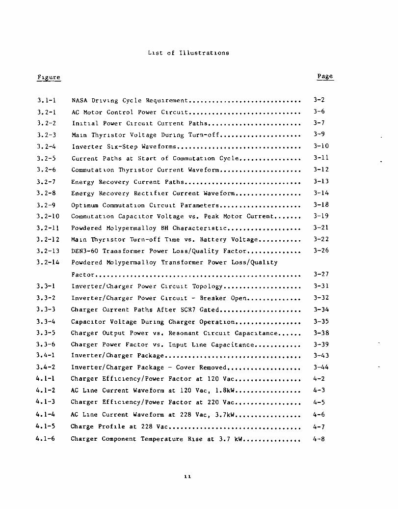
L1St of Illustrat10ns
NASA Dr1v1ng Cycle Requ1rement •••••••••••••••••••••••••••••
AC Motor Control Power C1rcu1t •••••••••••••••••••••••••••••
In1t1al Power C1rcu1t Current Paths ••••••••••••••••••••••••
Ma1n Thyr1stor Voltage Dur1ng Turn-off •••••••••••••••••••••
Inverter S1x-Step Waveforms ••••••••••••••••••••••••••••••••
Current Paths at Start of Commutat1on Cycle ••••••••••••••••
Commutatlon Thyr1stor Current Waveform •••••••••••••••••••••
Energy Recovery Current Paths ••••••••••••••••••••••••••••••
Energy Recovery Rect1f1er Current Waveform •••••••••••••••••
Opt1mum Commutat1on C1rcult Parameters •••••••••••••••••••••
Commutat1on Capac1tor Voltage vs. Peak Motor Current •••••••
Powdered Molypermalloy BH Character1st1c •••••••••••••••••••
Ma1n Thyr1stor Turn-off T1me vs. Battery Voltage •••••••••••
DEN3-60 Transformer Power Loss/Quality Factor ••••••••••••••
Powdered Mo1yperma11oy Transformer Power Loss/Qua11ty
Factor ..•.•...•.......••.....•.•......•.•..•.•••..•...••.••
Inverter/Charger Power C1rcu1t Topology ••••••••••••••••••••
Inverter/Charger Power C1rcu1t Breaker Open ••••••••••••••
Charger Current Paths After SCR7 Gated •••••••••••••••••••••
Capac1tor Voltage Dur1ng Charger Operat1on •••••••••••••••••
Charger Output Power vs. Resonant C1rcu1t Capac1tance ••••••
Charger Power Factor vs. Input L1ne Capacitance ••••••••••••
Inverter/Charger Package •.••.•.•..••..•...••••.•••.••••••••
Inverter/Charger Package - Cover Removed •••••••••••••••••••
Charger Eff1c1ency/Power Factor at 120 Vac •••••••••••••••••
AC L1ne Current Waveform at 120 Vac, 1.8kW •••••••••••••••••
Charger Eff1c1ency/Power Factor at 220 Vac •••••••••••••••••
AC L1ne Current Waveform at 228 Vac, 3.7kW •••••••••••••••••
Charge Prof1le at 228 Vac ••••••••••••••••••••••••••••••••••
Charger Component Temperature R1se at 3.7 kW •••••••••••••••
11
3-2
3-6
3-7
3-9
3-10
3-11
3-12
3-13
3-14
3-18
3-19
3-21
3-22
3-26
3-27
3-31
3-32
3-34
3-35
3-38
3-39
3-43
3-44
4-2
4-3
4-5
4-6
4-7
4-8
Figure
4.2-1
4.2-2
4.2-3
4.2-4
4.2-5
4.2-6
4.2-7
4.2-8
4.2-9
4.2-10
4.2-11
4.2-12
4.2-13
4.2-14
4.2-15
4.2-16
A-I
B-1
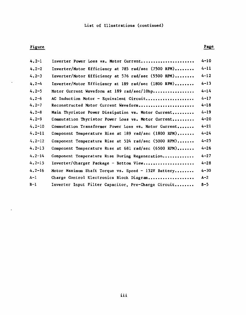
List of Illustrations (continued)
Inverter Power Loss vs. Motor Current ••••••••••••••••••••••
Inverter/Motor Efficiency at 785 rad/sec (7500 RPM) ••••••••
Inverter/Motor Efficiency at 576 rad/sec (5500 RPM) ••••••••
Inverter/Motor Efficiency at 189 rad/sec (1800 RPM) ••••••••
Motor Current Waveform at 189 rad/sec/l0hp •••••••••••••••••
AC Induction Motor - Equivalent Circuit ••••••••••••••••••••
Reconstructed Motor Current Waveform •••••••••••••••••••••••
Main Thyristor Power Dissipation vs. Motor Current •••••••••
Commutat~on Thyristor Power Loss vs. Motor Current •••••••••
Commutat~on Transformer Power Loss vs. Motor Current •••••••
Component Temperature Rise at 189 rad/sec (1800 RPM) •••••••
Component Temperature Rise at 524 rad/sec (5000 RPM) •••••••
Component Temperature ~se at 681 rad/sec (6500 RPM) •••••••
Component Temperature R1se During Regeneration •••••••••••••
Inverter/Charger Package - Bottom View •••••••••••••••••••••
Motor Maximum Shaft Torque vs. Speed - 132V Battery ••••••••
Charge Control Electronics Block Diagram •••••••••••••••••••
Inverter Input Filter Capacitor, Pre-Charge Circuit ••••••••
iii
4-10
4-11
4-12
4-13
4-14
4-17
4-18
4-19
4-20
4-21
4-24
4-25
4-26
4-27
4-28
4-30
A-2
B-5
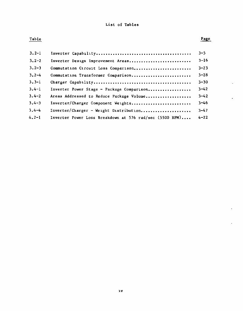
Table
3.2-1
3.2-2
3.2-3
3.2-4
3.3-1
3.4-1
3.4-2
3.4-3
3.4-4
4.2-1
List of Tables
Inverter Capablilty ••••••••••••••••••••••••••••••••••••••••
Inverter Deslgn Improvement Areas ••••••••••••••••••••••••••
Commutatlon Clrcult Loss Comparlson ••••••••••••••••••••••••
Commutatlon Transformer Comparison •••••••••••••••••••••••••
Charger Capab111.ty •••••.••••••••.•••••••••••••••••.••••••••
Inverter Power Stage - Package Comparlson ••••••••••••••••••
Areas Addressed to Reduce Package Volume •••••••••••••••••••
Inverter/Charger Component Welghts •••••••••••••••••••••••••
Inverter/Charger - Welght Dlstributl0n •••••••••••••••••••••
Inverter Power Loss Breakdown at 576 rad/sec (5500 RPM) ••••
lV
3-5
3-16
3-23
3-28
3-30
3-42
3-42
3-46
3-47
4-22
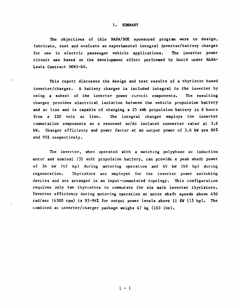
1. SUMMARY
The objectives of this NASA/DOE sponsored program were to design,
fabricate, test and evaluate an exper~ental integral inverter/battery charger
for use in electric passenger vehicle applications. The inverter power
circuit was based on the development effort performed by Gould under NASA
Lewis Contract DEN3-60.
This report discusses the design and test results of a thyristor based
inverter/charger. A battery charger is included integral to the inverter by
using a subset of the inverter power cl.rcuit components. The resulting
charger provides electrical isolation between the vehicle propulsion battery
and ac ll.ne and is capable of charging a 25 kWh propulsion battery in 8 hours
from a 220 volt ac line. The integral charger employs the inverter
commutation components as a resonant ac/dc isolated converter rated at 3.6
kW. Charger efficiency and power factor at an output power of 3.6 kW are 86%
and 95% respectively.
The inverter. when operated with a matchl.ng polyphase ac induction
motor and nominal 132 volt propUlsion battery, can provide a peak shaft power
of 34 kW (45 hp) during motoring operatl.on and 45 kW (60 hp) durl.ng
regeneration. Thyrl.stors are employed for the inverter power switching
devl.ces and are arranged in an input-commutated topology. This configuratl.on
requires only two thyrl.stors to commutate the six main inverter thyristors.
Inverter efficiency during motoring operation at motor shaft speeds above 450
rad/sec (4300 rpm) is 92-94% for output power levels above 11 KW (15 hp). The
combined ac l.nverter/charger package weighs 47 kg (103 lbs).
1 - 1
2. INTRODUCTION
2.1 Background
The Gould Research Center, Electron1cs Laboratory, completed 1n August
of 1980 the development of a first-generation experimental ac propulsion
system, for use 1n electr1c passenger vehicles. The ac propulsion system
consisted of an 1nverter, an ac 1nduct1on motor and the associated control
electronics. This experimental development effort was sponsored by the U.S.
Department of Energy and managed by the NASA-Lew1s Research Center under Con
tract DEN3-60. In August of 1981, development of a second generation
experimental inverter was initiated under NASA-LewlS Contract DEN3-249. The
contract objectives were to modify the DEN3-60 inverter power stage topology
to 1nclude a battery charger, increase the 1nverter power capability to
provlde a vehicle with diesel equ1valent acceleration performance and reduce
the we1ght and volume of the combined inverter/charger power stage.
Both 1nverters ut11ize state-of-the-art thyr1stor power semiconductors
and m1croprocessor based control circuitry to regulate the speed and torque of
a conventlOnal squirrel cage polyphase ac induction motor. The motoring
control electronics developed during NASA-LewlS Contract DEN3-60 was used 1n
the development of the DEN3-249 1nverter. To real1ze the 1ncreased power
capability of the DEN3-249 1nverter the motor1ng control electron1cs must be
ta1lored to the operat1ng character1stics of the ac induction motor.
Performance uS1ng the DEN3-60 motoring control electronics only allows
inverter operation 1n non-veh1cle driving regimes. Charge control electron1cs
was developed for use with the integral on-board battery charger and added to
the system dur1ng the second contract.
2.2 Object1ves
The speclflc objectives of this contract were:
1. Incorporate an lsolated 3 kW on-board battery charger into the
existing inverter design.
2 - 1
2. Increase the inverter peak power capability from 26 kW (35 hp) to 34
kW (45 ph).
3. Reduce the volume and weight of the inverter power stage developed
under Contract DEN3-60 by 50% and 30%, respectively.
2.3 Scope
The contract work scope consisted of the design, fabrication, test,
evaluation and delivery of a combined exper~mental inverter and battery
charger power stage for use ~n electric vehicle applicat~ons. The motoring
control electronics developed during NASA-Lewis Contract DEN3-60 and a
standard ac induction motor were used to test and evaluate the new ~nverter
power stage. Charge control electronics was developed for use w~th the
integral on-board battery charger.
2 - 2
3. ANALYSIS AND DESIGN
3.1 Inverter/Charger Requirements
The design of the inverter and integral onboard battery charger was
based on the following requirements.
3.1.1 Inverter
The power handling requirements of the inverter power stage were
established by five vehicle operating modes;
Repetit1.ve operation per the SAE-J227a, Schedule D driving cycle shown in
Figure 3.1-1,
Steady-state operation at a motor shaft power of 11.2 kW (15hp) which
corresponds to vehicle operation at a constant 88.5 km/h (55 mph),
Operation at a motor shaft power of 26.1 kW (35 hp) for 30 seconds which
corresponds to vehicle operation at 48.3 km/h (30 mph) on a 10% grade,
Operat1.on at an average motor shaft power of 33.6 kW (45 hp) for 16 seconds
which corresponds to vehicle acceleration from 40.2 - 88.5 km/h (25-55 mph),
Operation at a motor shaft torque of 60 N-m and an average shaft power of 29.8
kW (40 hp) for a total of 8 seconds which corresponds to a diesel equivalent
veh1.cle acceleration from 0-48.3 km/h (0-30 mph).
The inverter loS also to have the capacity to provide regenerative
energy to the propulsion battery, be self-protecting, interface with existing
and 1.mproved lead-acid battery sources and operate over an ambient temperature
range of -34°C to 49°C.
3 - 1
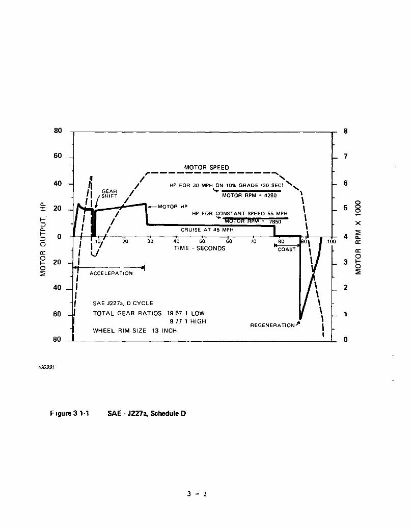
80 8
60 7
MOTOR SPEED
r--------------~ 40 11
/ , 6 / HP FOR 30 MPH ON 10% GRADE (30 SEC) "
II GEAR // '-to MOTOR RPM ; 4280 \ /SHIFT 0.. I I 0
20 -MOTOR HP \ 5 0 I 0 / HP FOR CONSTANT SPEED 55 MPH
\ t- / ..
ItlI~T~J!!I J!!II!IItlI - 7850 ::) \ X 0.. / CRUISE AT 45 MPH t- O 4
~ ::) 0..
0 I 20 30 40 50 60 70 100 a: TIME - SECONDS
a: I a: 0 0 20 I 3 t-t-
O ---4f 0 ~ ACCE LEPA TlON ~
I 40 I 2
I I SAE J227a, D CYCLE
60 ,
TOTAL GEAR RATIOS 1957 1 LOW 1 977 1 HIGH
REGENERATION ~ WHEEL RIM SIZE 13 INCH
80 0
(0699)
Figure 31-1 SAE - J227a, Schedule 0
3 - 2
3.1.2 Battery Charger
The des1gn of the battery charger was based on the follow1ng
requ1rementsj
The charger 1S to be an 1ntegral part of the 1nverter and ut111ze the eX1st1ng
power and control c1rcu1try to the greatest extent poss1ble.
The charger 1S to have the capab1l1ty of charg1ng a completely d1scharged
lead-ac1d battery from a nom1nal 220 volt, 60 Hz, s1ngle phase res1dential
power source 1n less than 8 hours. Charger operat1on from a nom1nal 120 volt,
60 Hz ac line 1S also des1red.
The battery 18 to be 1solated from the ac llne power source to prevent
electr1c shock hazards to operat1ng personnel.
3 - 3
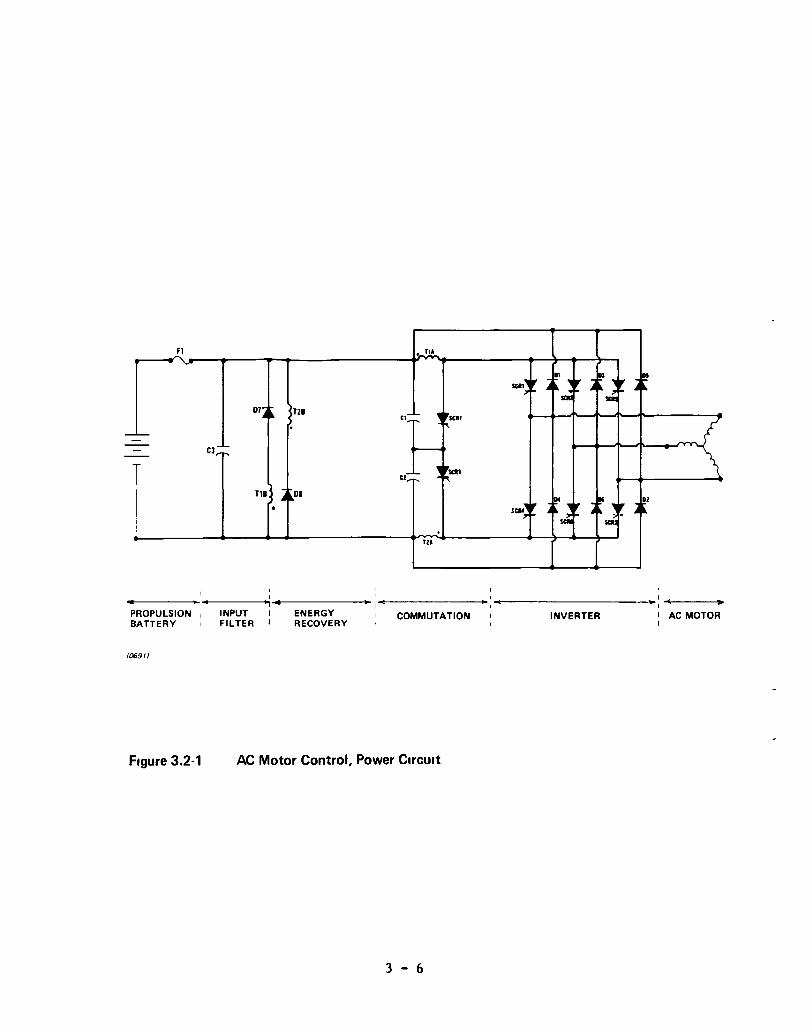
3.2 Inverter
The lnverter power Clrcult topology lS presented and ltS operatlon
descrlbed. The deslgn areas addressed to lncrease the lnverter power capa-
blilty and efflclency are presented. The capablilty of the new lnverter power
stage, compared to the OEN3-60 lnverter, lS presented ln Table 3.2-1.
3.2.1 Clrcult Operatlon
The lnput-commutated lnverter ClrCUlt topology developed durlng thlS
contract lS presented ln Flgure 3.2-1. The baslc goal of mlnlmum materlals
cost glves the lnput-commutated topo logy an lmportant advantage compared to
most alternatlve thyrlstor lnverter conflguratlons as lt contalns fewer power
components. ThlS lnverter topology requlres only two commutatlon clrcults,
one for the posltlve bus and one for the negatlve bus, to commutate all SlX
maln thyrlstors ln the three-phase brldge.
The power sWltchlng stage shown ln Flgure 3.2-1 allows connectlon of
each of the three motor llnes to either the posltlve or negatlve battery
termlnal. The actual conductlon paths are provlded by the maln thyrlstors
(SCRl-6) and the freewheellng rectlflers (01-6). The remalnlng semlconductors
(SCR7,8, 07,8), transformers (TI,2) and capacltors (CI,2) are lnvolved ln the
commutatlon (turn-off) of the maln thyrlstors. ThlS commutatlon clrcultry lS
necessary to dlvert the motor current from a conducting maln thyrlstor so that
lt wlll regaln ltS voltage blocklng capablllty. Capacltor C3 provldes a low
lmpedance path ln parallel wlth the battery for the maln lnverter and
commutatlon Clrcult current.
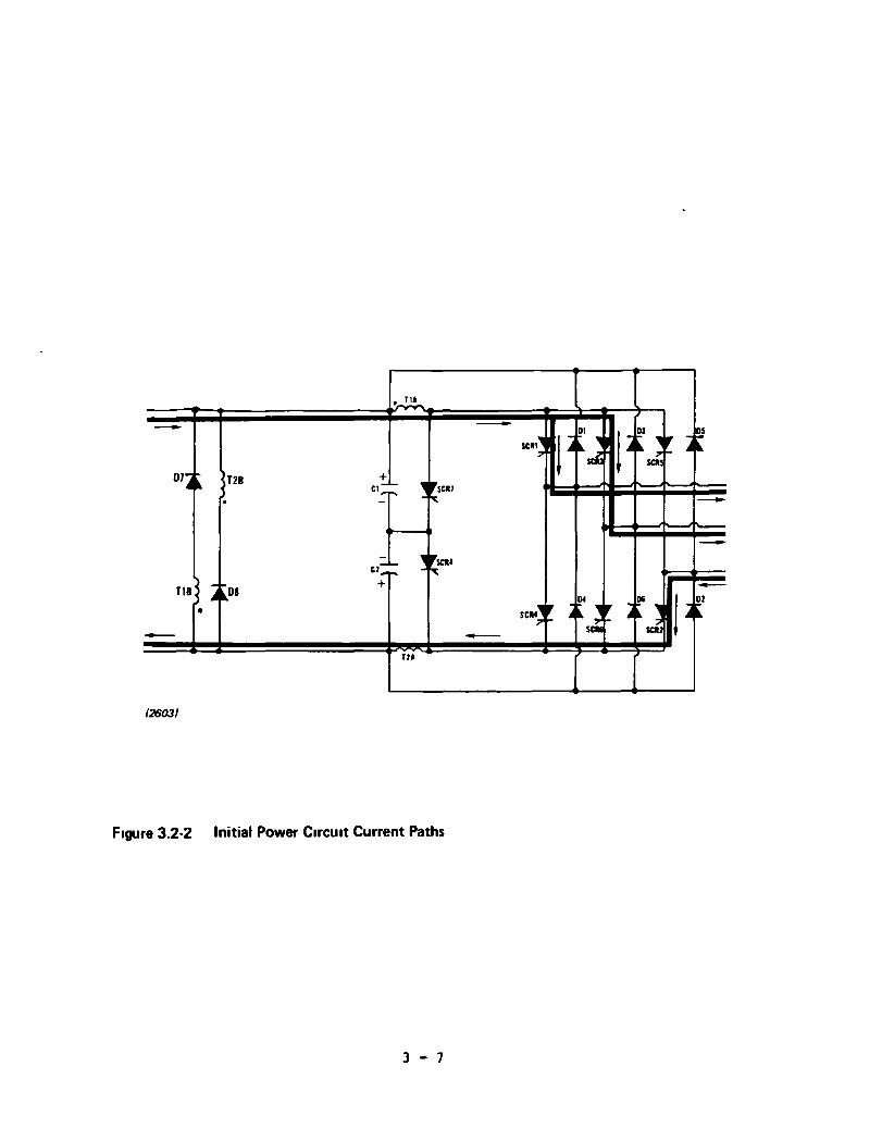
The power Clrcult lnltlal condltlons are presented ln Flgure 3.2-2 wlth
maln thyrlstors SCRI, 2 and 3 conductlng current. It lS deslred to commutate
SCRI and turn on SCR4. Capacltors CI and Cl have been charged wlth voltage
polarltles as lndlcated. Commutatlon thyrlstor SCR7 lS gated on, placlng the
lnltlal capacltor voltage, Voc, across transformer wlndlng, TIA. If the
voltage across wlndlng TIA lS greater than the battery voltage, VB, then maln
3 - 4
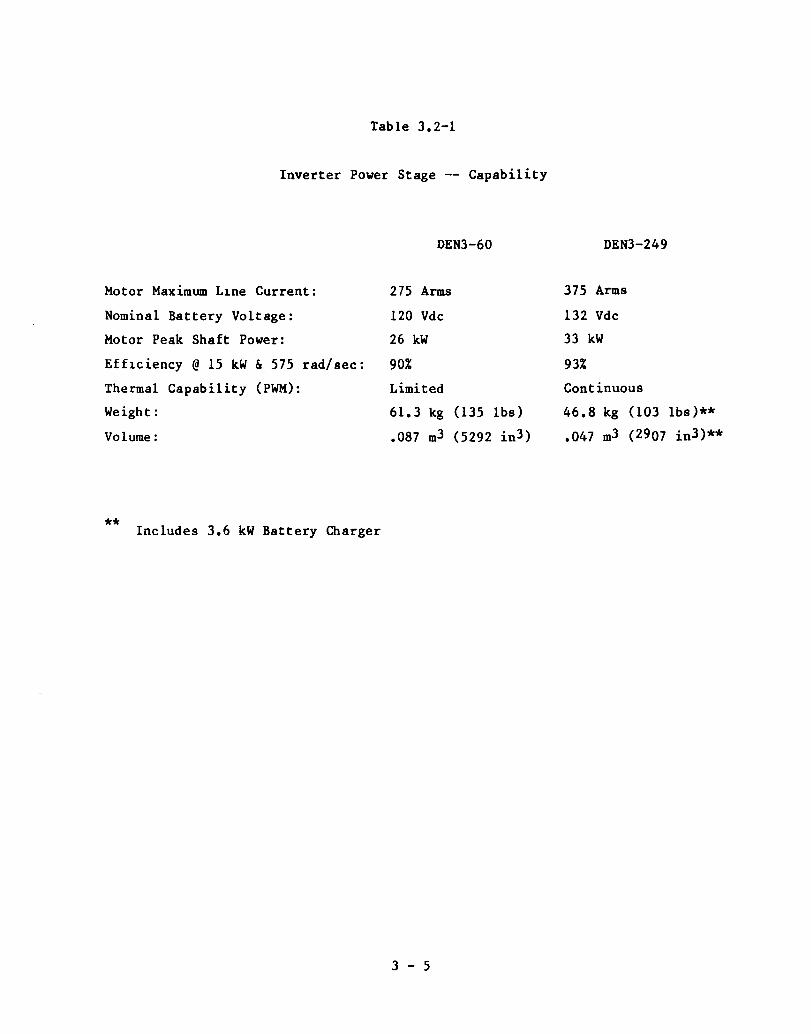
Table 3.2-1
Inverter Power Stage -- Capability
DEN3-60 DEN3-249
Motor Maximum L1ne Current: 275 Arms 375 Arms
Nominal Battery Voltage: 120 Vdc 132 Vdc
Motor Peak Shaft Power: 26 kW 33 kW
Eff1ciency @ 15 kW & 575 rad/sec: 90% 93%
Thermal Capability (PWM): Limited Continuous
Weight: 61.3 kg (135 lbs) 46.8 kg (103 lbs)**
Volume: .087 m3 (5292 in3) .047 m3 (2907 in3)**
** Includes 3.6 kW Battery Charger
3 - 5
CI "l~SC.' --
HI
I I I I I
··~-------·I~·~------~·f~·~----------+· ,~~~------------" I-C~------------------~.,~<~----~~ PROPULSION I INPUT BATTERY FILTER
1(691)
ENERGY RECOVERY
COMMUTATION
Figure 3.2-' AC Motor Control, Power Circuit
3 - 6
INVERTER 1 AC MOTOR
.~
- - ! ~ D.
l~ OJ ,
~ ~ ~ SCR.' ~ , Ira. ? ~ ? '~
SCI!
D7~ ~ )121 + C,-- ~ 'SCR' . ' .......
"" --
Cl:;~ ~ 'SCII. ~ TIl ~ -~D8 + -) A D4 ,. -III ~ I ~ ~l • SCR4~ ~ .4 ~s1 '";1' f- .4 ~ -? ~
- - SCI!
TlJ
1 (2603)
Figure 3.2-2 Initial Power Circuit Current Paths
3 - 7
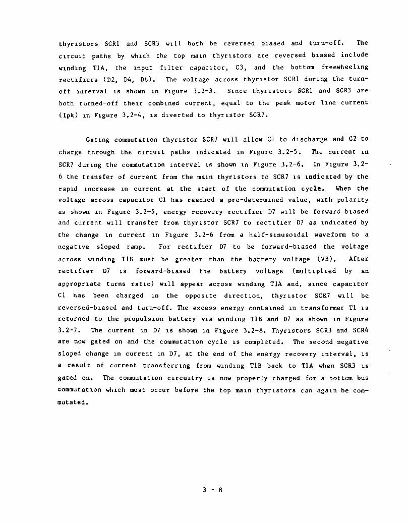
thyr1stors SCRI and SCR3 w1ll both be reversed b1ased and turn-off. The
CHcult paths by Wh1Ch the top maw thyr1stors are reversed b1ased include
wlndlng TIA, the lnput fllter capacltor, C3, and the bottom freewheellng
rect1hers (D2, D4, D6). The voltage across thyr1stor SCRI dur1ng the turn
off lnterval lS shown ln F1gure 3.2-3. Slnce thyr1stors SCRI and SCR3 are
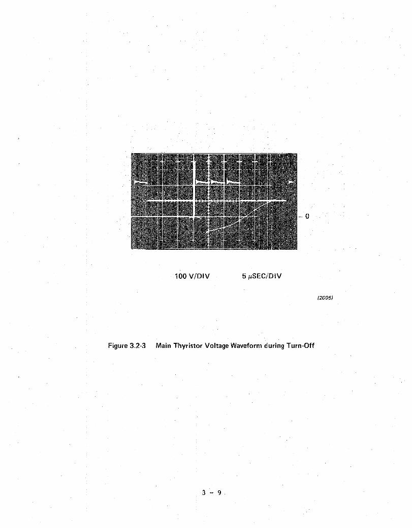
both turned-off the1r comblned current, equal to the peak motor llne current
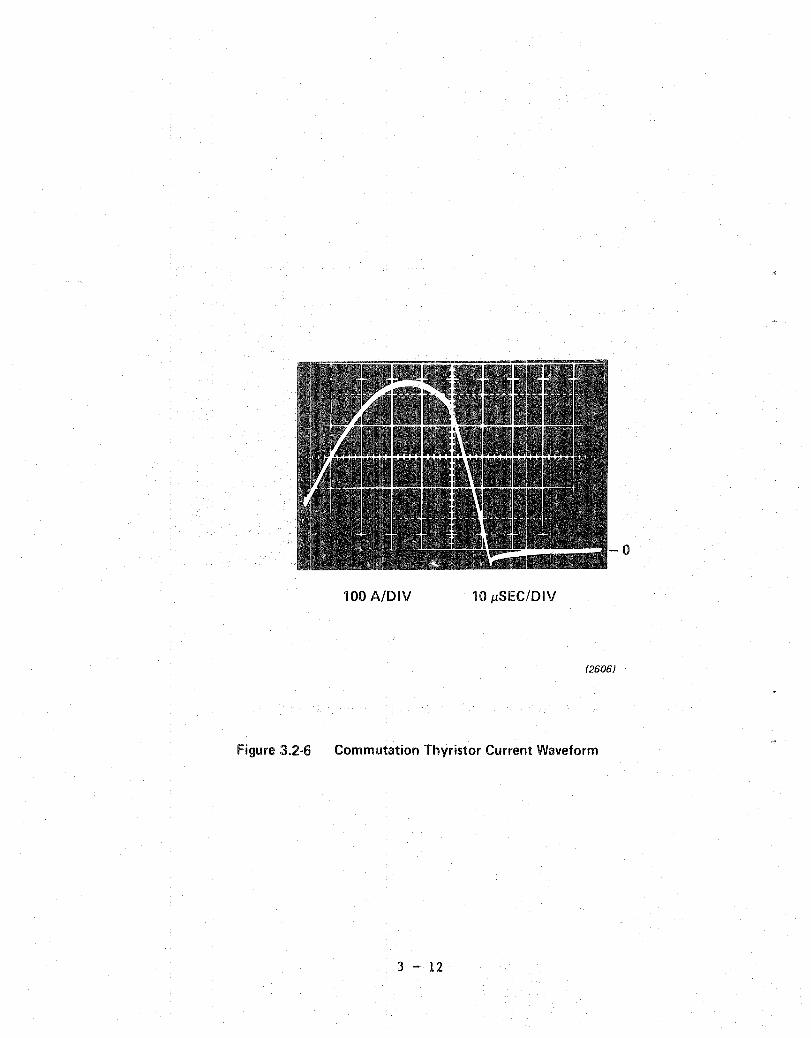
(Ipk) 1n Flgure 3.2-4, 1S dlverted to thyr1stor SCR7.
Gatlng commutatlon thyrlstor SCR7 wlll allow CI to dlscharge and C2 to
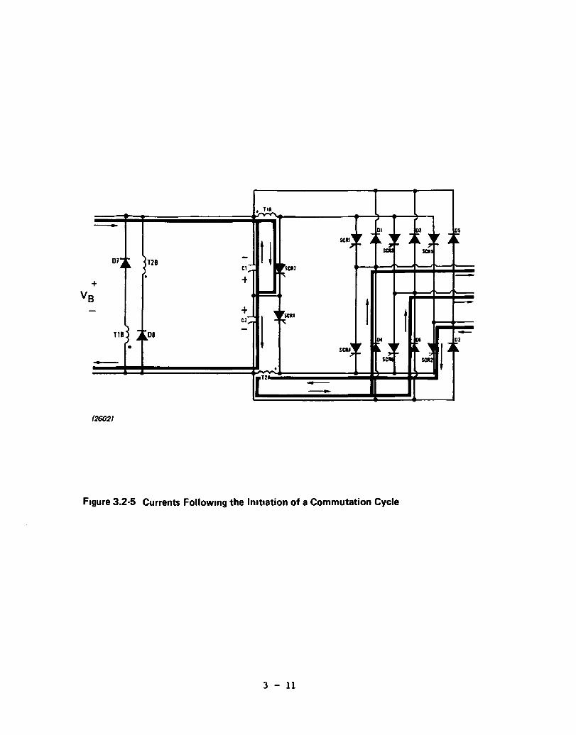
charge through the C1rcu1t paths lndlcated In Flgure 3.2-5. The current In
SCR7 durlng the commutatlon lnterval lS shown ln Flgure 3.2-6. In Flgure 3.2-
6 the transfer of current from the maln thyrlstors to SCR7 lS lndicated by the
rapld lncrease ln current at the start of the commutation cycle. When the
voltage across capac1tor CI has reached a pre-determ1ned value, wlth polar1ty
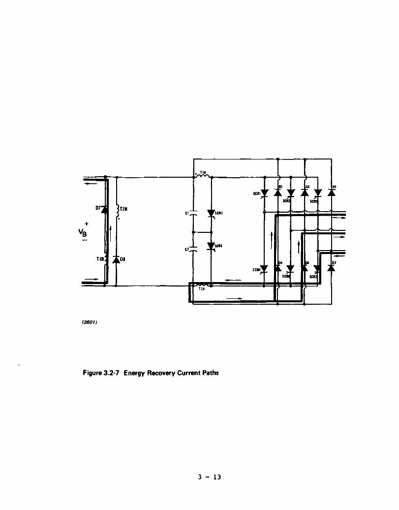
as shown 1n Flgure 3.2-5, energy recovery rect1f1er D7 w1ll be forward b1ased
and current wlll transfer from thyrlstor SCR7 to rect1fler D7 as lnd1cated by
the change In current ln Flgure 3.2-6 from a half-s1nusoldal waveform to a
negatLVe sloped ramp. For rect1fLer D7 to be forward-blased the voltage
across wlndlng TIB must be greater than the battery voltage (VB). After
rect1fler D7 1S forward-blased the battery voltage (multlplled by an
appropr1ate turns ratlo) wlll appear across w1nd1ng TIA and, Slnce capac1tor
Cl has been charged 1n the Oppos1te d1rect10n, thyr1stor SCR7 wlll be
reversed-b1ased and turn-off. The excess energy contalned 1n transformer TI lS
returned to the propulslon battery Vla wlndlng TlB and D7 as shown ln Flgure
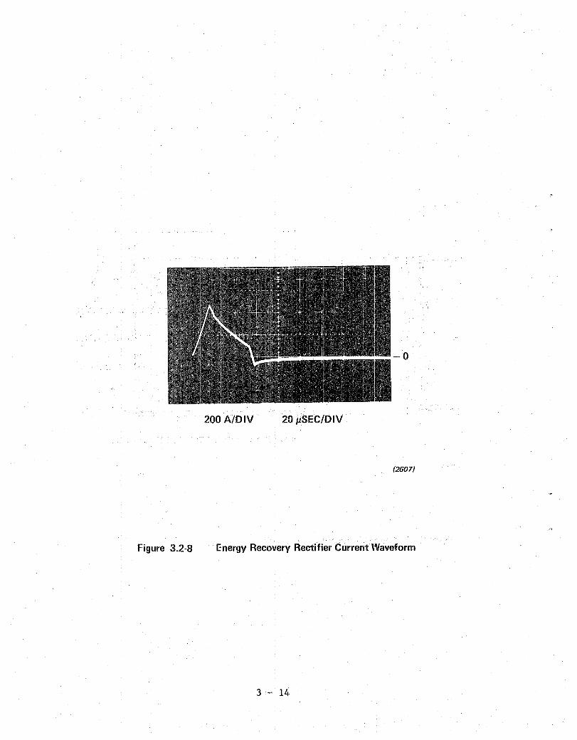
3.2-7. The current ln D7 l8 shown ln Flgure 3.2-8. ThyrLStors SCR3 and SCR4
are now gated on and the commutatlon cycle 1S completed. The second negatlve
sloped change 1n current ln D7, at the end of the energy recovery lnterval, 1S
a result of current transferr1ng from w1ndlng TIB back to TIA when SCR3 lS
gated on. The commutatlon clrcultry lS now properly charged for a bottom bus
commutat10n wn1ch must occur before the top maln thyr1stors can aga1n be com
mutated.
3 - 8
-0
100 V/DIV 5I1SEC/DIV
(2605)
Figure 3.2-3 Main Thyristor Voltage Waveform during Turn-Off
3 - 9
MOTOR LINE CURRENT (200A/DIV)
MOTOR LIN NE VOLTAGE (200V/DIV)
Figure 3.2-4
o
o
Motor Une Current and Line· Line Voltage
(Six· Step Operation)
3 - 10
(2604)
.~ 1 - ~ "4 SCRl~
,. - Dl "4 ,. - r -~
t 1 .~ ~ ..,j "sc:; f. ~ ~ ;1 ~ ~
SCI!
01- -',4 ~ T28
Cl; ~SCRl . + -+ .... "--
t r---
+ I ~ ~SCR' t C2::
T18 ~ roDe - -~L
SCR4"4 , D4 , !Ii
I • ~2
• ~sc~ ~ ~ ~ ";1 ~ ~ - SCR . r
T2 --(2602)
Figure 3.2-5 Currents Following the Initiation of a Commutation Cycle
3 - 11
o
100 A/DIV 10/lSEC/DIV
(2606)
Figure 3.2-6 Commutation Thyristor Current Waveform
3 - 12
~ - 10. ~ SCI." ~ ~ ~ ~
~ ., ~ ~ ~ ":- ~sJ ~ -~ ~
SCI
Dl~ ~T21 C'::~ ., ~SCR7 >. -+
f B
f --Cl:::::: ~ ~SCI' t
TIl -~DI -~ ~.
SCI4" ,
1M " ,.
III " ~ Dl
-:- ~ ~ SC~ -. .? ..
SCI - -TU
-(2601)
Figure 3.2-7 Energy Recovery Current Paths
3 - 13
-0
200 A/DIV 20 j.LSEC/DIV
(2607)
Figure 3.2-8 Energy Recovery Rectifier Current Waveform
3 - 14
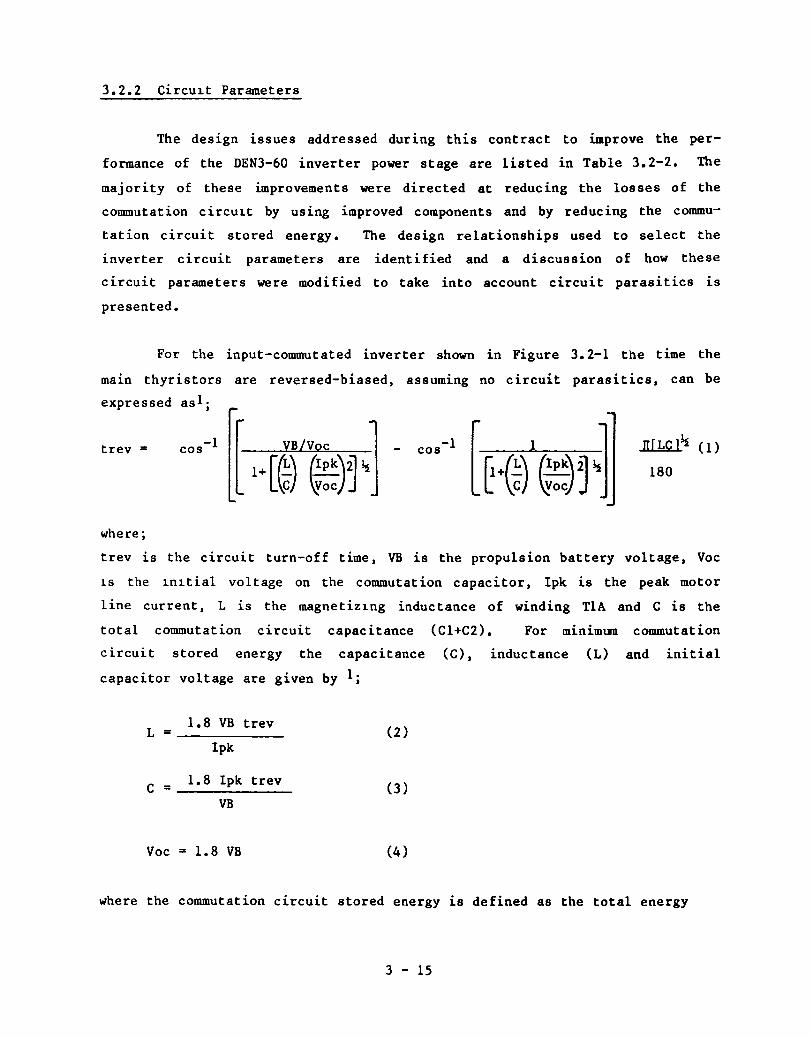
3.2.2 Circu1t Parameters
The design issues addressed during this contract to improve the per
formance of the DEN3-60 inverter power stage are listed in Table 3.2-2. The
majority of these improvements were directed at reducing the losses of the
commutation circu1t by using improved components and by reducing the commu
tation circuit stored energy. The design relationships used to select the
inverter circuit parameters are identified and a discussion of how these
circuit parameters were modified to take into account circuit parasitics is
presented.
For the input-commutated inverter shown in Figure 3.2-1 the time the
main thyristors are reversed-biased, assuming no circuit parasitics, can be
expressed as 1 ;
trev =
where;
nlLC )~ (l)
180
trev is the circuit turn-off time, VB is the propulsion battery voltage, Voc
18 the 1n1tial voltage on the commutation capacitor, Ipk is the peak motor
line current, L is the magnetiZ1ng inductance of winding T1A and C is the
total commutation circuit capacitance (C1+C2). For minimum commutation
circuit stored energy the capacitance (C), inductance (L) and initial
capacitor voltage are given by 1;
1.8 VB trev L = (2)
Ipk
C = 1.8 Ipk trev (3)
VB
Voc = 1.8 VB (4)
where the commutation circuit stored energy is defined as the total energy
3 - 15
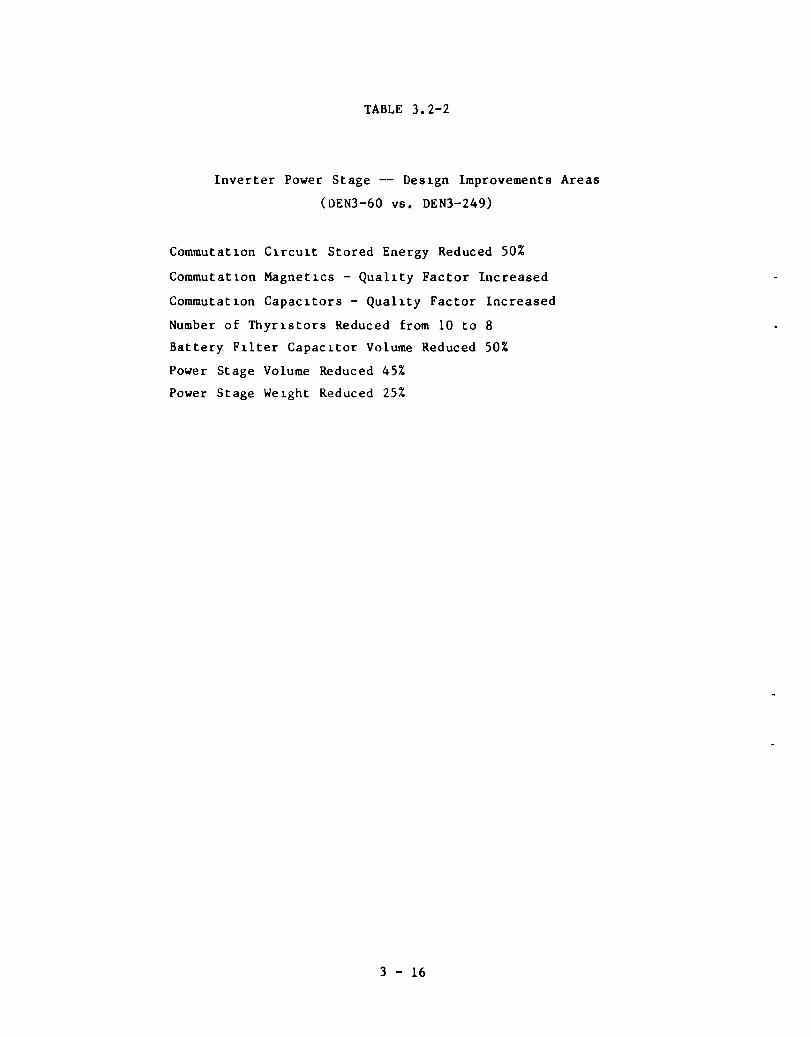
TABLE 3.2-2
Inverter Power Stage -- Deslgn Improvements Areas
(OEN3-60 vs. DEN3-249)
Commutatlon Clrcult Stored Energy Reduced 50%
Commutatlon Magnetlcs - Quahty Factor Increased
Commutatlon Capacltors - Quallty Factor Increased
Number of Thyrlstors Reduced from 10 to 8
Battery Fllter Capacltor Volume Reduced 50%
Power Stage Volume Reduced 45i.
Power Stage Welght Reduced 25%
3 - 16
stored 1n Land C and 1S a funct10n of the peak motor current (wh1ch 1S also
the inverter bus current) and 1n1tial capac1tor voltage as given by;
Es = ~ CVoc 2 + ~ Llpk2 (S)
The commutation circu1t component values for min1mum stored energy are
presented in Figure 3.2-9 as a function of the peak motor line current (Ipk)
for a battery term1nal voltage of 120 volts and a ma1n thyristor reverse-bias
t 1me of 14 usec. The ma1n thyr1stors selected were General Electr1c C384M
dev1ces hav1ng a max1mum spec1f1ed turn-off t1me of 10 usec at a junction
temperature of 125°C. The nom1nal battery voltage 1S 132 volts, however
dur1ng motor1ng operation the battery term1nal voltage decreases due to the
battery internal res1stance. The actual component values were selected for
m1n1mum stored energy at the peak motor current ant1c1pated dur1ng vehicle
operat1on at IShp (1.e. Ipk = 200-300 Amps) as opposed to vehicle operat10n at
45 hp (1.e., 700 amps). The values selected were a total commutation
capac1tance (C) of 56 uf and a TIA magnet1z1ng 1nductance (L) of 11 uh.
Due to the finite leakage 1nductance eX1st1ng between the transformer A
and B w1nd1ngs and the paras1tic 1nductance present 1n the commutat10n
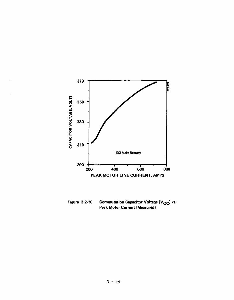
c1rcu1t, the init1al capacitor voltage (Voe) increases with increasing motor
current as shown 1n F1gure 3.2-10. Th1S second order effect allowed the
commutat10n C1rcu1t parameters to be selected for effic1ent operation at 15 hp
whlle also having the capab1l1ty to commutate the main thyristors at 4S hp.
The penalty 1S 1ncreased commutat1on losses at the higher power levels,
however, operation at these power levels (1.e., 45 hp) 1S only required for 16
seconds. The advantage is more effic1ent operat10n at IS hp.
Under ideal cond1tions the capac1tor voltage will rema1n constant at
216 volts 1ndependent of motor current however, as stated previously the ca
pac1tor voltage increases with increas1ng motor current due to the leakage
inductance between the transformer A and B windings. This leakage inductance
results in an overshoot 1n the capacitor voltage that 1S a funct10n of the
energy stored in the commutation circu1t. Under 1deal conditions the capaci
tor voltage is given by equat10n 6;
3 - 17
32 160 ~~~-------------------------------, i
24 120
16 80
8 40
o
VB =120V
tREY = 14 Ilsec
L
200 400 600 800
PEAK MOTOR LINE CURRENT, AMPS
~
1000
Figure 3.2-9 Optimum Commutation Circuit Parameters Based on Minimum
Stored Energy
3 - 18
en I...I o > w' CJ
~ ...I
~ a:: o I-
~ ~ (.)
370
350
330
310
290
132 Volt Battery
200 400 600 800
PEAK MOTOR LINE CURRENT, AMPS
FIgure 3.2·10 Commutation Capacitor Voltage (Voc) VS.
Peak Motor Current (Measured)
3 - 19
Voc = VB (1 + NA/NB) (6 )
where NA lS the number of turns on the A wlnding and NB lS the number of turns
on the B wlndlng.
equatlon 7 below;
The overshoot ln capacltor voltage can be approx1mated by
flVoc = r2 Esl ~ [ NA] [Lstray1 ~ L L J NA + NB C J
(7)
where Lstray lS equal to the leakage inductance between the transformer A and
B w1ndlngs (l.8 uh) and the paras1tlc inductance present in the commutation
Clrcult (1.0 uh). Based on ideal conditlons and uS1ng equatlOn 6 the turns
ratlo (NA/NB) lS equal to 0.8. At a peak motor current of 200 amps the calcu
lated overshoot 10 the commutat10n capacltor voltage lS 66 volts for an in1-
tlal capacltor voltage of 282 volts (Voc + flVoc). As the peak motor current
lncreases above 200 amps the current ln the A w1ndlng also increases result1ng
ln a further lncrease 1n the commutatlon capacitor overshoot.
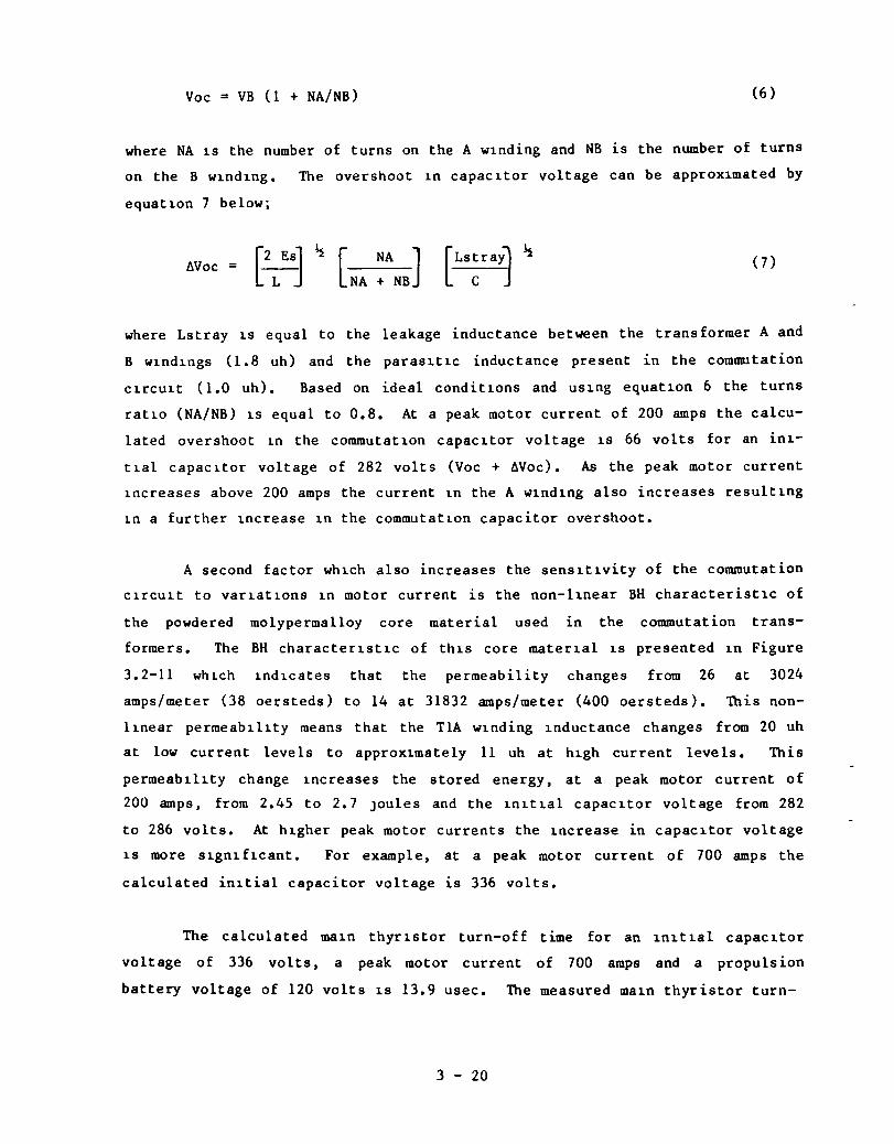
A second factor WhlCh also increases the sensltlvity of the commutation
C1rcult to varlatlons ln motor current is the non-llnear BH characteristlc of
the powdered molypermalloy core material used in the commutation trans
formers. The BH characterlstlc of th1.S core mater1.al lS presented ln Figure
3.2-11 wh1.ch 1.nd1.cates that the permeability changes from 26 at 3024
amps/meter (38 oersteds) to 14 at 31832 amps/meter (400 oersteds). This non-
11.near permeab1.l1.ty means that the T1A wlnding 1.nductance changes from 20 uh
at low current leve ls to approx1.mate ly 11 uh at h1.gh current leve Is. This
permeablllty change 1.ncreases the stored energy, at a peak motor current of
200 amps, from 2.45 to 2.7 Joules and the 1.n1.t1.al capacltor voltage from 282
to 286 volts. At h1.gher peak motor currents the 1.ncrease in capac1.tor voltage
1.S more s1.gnlhcant. For example, at a peak motor current of 700 amps the
calculated in1.tial capacitor voltage 1.S 336 volts.
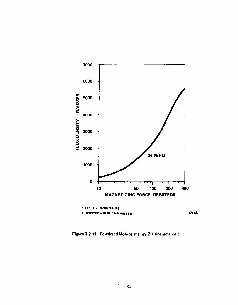
The calculated maln thyr1.stor turn-off time for an 1nlt1.al capac1tor
voltage of 336 volts, a peak motor current of 700 amps and a propulsion
battery voltage of 120 volts 1S 13.9 usec. The measured ma1n thyristor turn-
3 - 20
7000
6000
CI) w 5000 ~ =» c( 0 . 4000
> ~ CI)
z 3000 w 0 X ~ ...J
2000 ~
1000
o 10 50 100 200 400
MAGNETIZING FORCE, OERSTEDS
1 TESLA - 10.000 GAUSS
1 OERSTED - 79.58 AMPS/METER (2618)
Figure 3.2·11 Powdered Molypermalloy BH Characteristic
3 - 21
20
-__ -------------;I(PKI. 300 A -16
__ -------------;I(PKI· 500 A -_ ............................... __ ............ --~I(PKI .. 700 A
~ 12
- - - - - -- GE C384 TURN-OFF TIME - MINIMUM
8 95 100 105 110 115 120 125 130 135 140
PROPULSION BATTERY VOLTAGE, VOLTS
(2594)
Figure 3.2·12 Main ThYrIStor Turn-Off Time vs. Battery Voltage (Measured)
3 - 22
off time as a funct10n of peak motor current and propulsion battery voltage is
shown in Figure 3.2-12.
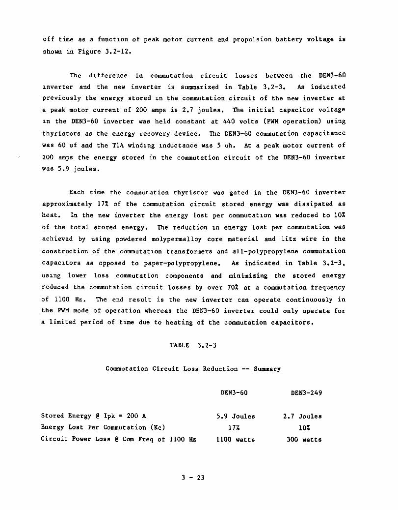
The d1fference in commutation circuit losses between the DEN3-60
1nverter and the new inverter is summarized in Table 3.2-3. As ind1cated
previously the energy stored 1n the commutation circuit of the new inverter at
a peak motor current of 200 amps is 2.7 joules. The initial capacitor voltage
1n the DEN3-60 inverter was held constant at 440 volts (PWM operation) using
thyristors as the energy recovery device. The DEN3-60 commutation capacitance
was 60 uf and the T1A wind1ng 1nductance was 5 uh. At a peak motor current of
200 amps the energy stored in the commutation circuit of the DEN3-60 inverter
was 5.9 joules.
Each time the commutation thyristor was gated in the DEN3-60 inverter
approximately 17% of the commutation circuit stored energy was dissipated as
heat. In the new inverter the energy lost per commutat10n was reduced to 10%
of the total stored energy. The reduction 1n energy lost per commutation was
achieved by using powdered molypermalloy core material and litz wire in the
construction of the commutat10n transformers and all-polypropylene commutation
capac1tors as opposed to paper-polypropylene. As indicated in Table 3.2-3,
uS1ng lower loss commutation components and minimizing the stored energy
reduced the commutation circuit losses by over 70% at a commutation frequency
of 1100 Hz. The end result is the new inverter can operate continuously in
the PWM mode of operation whereas the DEN3-60 inverter could only operate for
a limited period of t1me due to heating of the commutation capacitors.
TABLE 3.2-3
Commutation Circuit Loss Reduction -- Summary
Stored Energy @ Ipk = 200 A
Energy Lost Per Commutation (Kc)
Circuit Power Loss @ Com Freq of 1100 Hz
3 - 23
DEN3-60
5.9 Joules
17%
1100 watts
DEN3-249
2.7 Joules
10%
300 watts
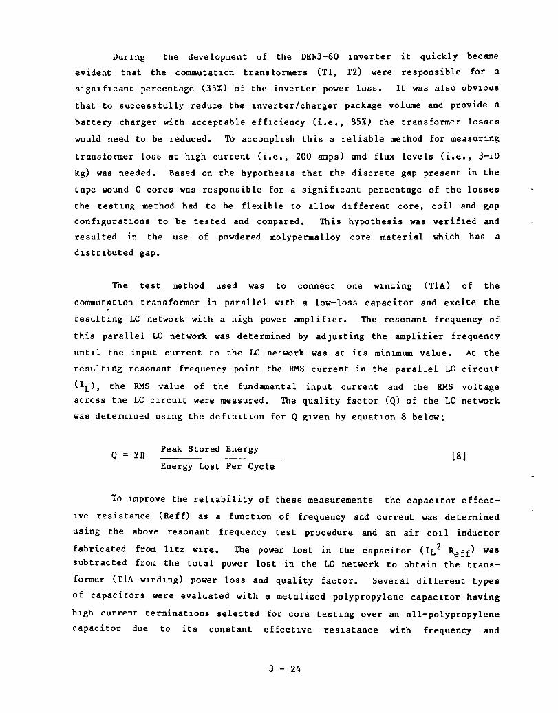
Dur1ng the development of the DEN3-60 1nverter it quickly became
evident that the commutat10n transformers (Tl, T2) were responsible for a
s1gn1f1cant percentage (35%) of the inverter power loss. It was also obv10us
that to successfully reduce the 1nverter/charger package volume and provide a
battery charger with acceptable eff1ciency (i.e., 85%) the transformer losses
would need to be reduced. To accomp11sh this a reliable method for measur1ng
transformer loss at h1gh current (i.e., 200 amps) and flux levels (i.e., 3-10
kg) was needed. Based on the hypothes1s that the discrete gap present in the
tape wound C cores was responsible for a signif1cant percentage of the losses
the test1ng method had to be flexible to allow ddferent core, coil and gap
conhgurat10ns to be tested and compared. This hypothesis was verif1ed and
resulted 1n the use of powdered molypermalloy core material which has a
d1str1buted gap.
The test method used was to connect one w1nding (TlA) of the
commutat10n transformer in parallel w1th a low-loss capacitor and excite the
resulting LC network with a high power ampliher. The resonant frequency of
this parallel LC network was determined by adjusting the amplifier frequency
unt11 the input current to the LC network was at its m1n1mum value. At the
result1ng resonant frequency point the RMS current 1n the parallel LC circu1t
(IL), the RMS value of the fundamental input current and the RMS voltage across the LC C1rcu1t were measured. The quality factor (Q) of the LC network
was determ1ned uS1ng the def1n1tion for Q g1ven by equat10n 8 below;
Q = 2JI Peak Stored Energy
[8] Energy Lost Per Cycle
To 1mprove the re11ability of these measurements the capac1tor effect-
1ve resistance (Ref£) as a funct10n of frequency and current was determined
using the above resonant frequency test procedure and an air co11 inductor
fabricated from htz wue. The power lost in the capacitor (IL 2 Reff) was
subtracted from the total power lost in the LC network to obtain the trans-
former (TlA w1nd1ng) power loss and quality factor. Several different types
of capacitors were evaluated with a metalized polypropylene capac1tor having
h1gh current terminat10ns selected for core test1ng over an all-polypropylene
capacitor due to its constant effect1ve res1stance with frequency and
3 - 24
current. The RMS value of the fundamental lnput current was measured using a
Princeton Applled Research lock-ln ampllfler (Model 5204). The lock-in
ampllfler was requlred due to the thlrd harmonlc lnput current produced by the
core non-llnear BH characterlstlc, especlally wlth the powdered molypermalloy
mater lal.
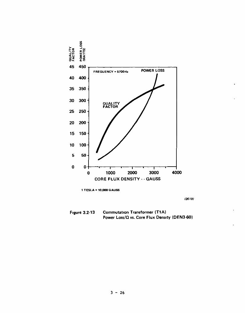
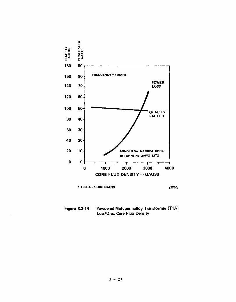
The measured power loss and quallty factor for the commutatlon
transformer (TIA wlndlng) used ln the DEN3-60 lnverter and a comparable
transformer constructed uSlng powdered molypermalloy core materlal and Iltz
wue lS presented In Flgures 3.2-13 and 3.2-14 respectlvely. The slgnlficant
lncrease in quallty factor obtalned uSlng the powdered molypermalloy core
materlal lS eVldent. Based on separate tests per formed uSlng the DEN3-60
transformer core materlal (2 mll slllcon-lron), lt was determlned that
approxlmately 50% of the transformer losses were attrlbutable to core and cOlI
losses resultlng from frlnglng flelds at the gap. The results are summarlzed
In Table 3.2-4.
3 - 25
~ >a:
0 ..J_
to a: Ul ..J~ W~ o(u ~~ :>0( 00( OLL ~~
45 450 FREQUENCY = 5700Hz POWER LOSS
40 400
35 350
30 300
25 250
20 200
15 150
10 100
5 50
o 1000 2000 3000 4000
CORE FLUX DENSITY· . GAUSS
1 TESLA· 10,000 GAUSS
(2619)
Figure 3.2·13 Commutation Transformer (Tl A) Power Loss/Q vs. Core Flux Density (DEN3·60)
3 - 26
~ >a:
0 -1-
!:o a: In -II- wI-c(CJ ~I-:lc( oct au. a..!
180 90
160 80
140 70
120 60
100 50
80 40
60 30
40 20
20 10
0 0
0
FREQUENCY = 4700 Hz
1000
POWER LOSS
QUALITY FACTOR
ARNOLD No A·129054 CORE
19 TURNS No 2AWG LITZ
2000 3000 4000
CORE FLUX DENSITY· - GAUSS
1 TESLA - 10,000 GAUSS (2620)
FIgure 3.2-14 Powdered Molypermalloy Transformer (T1A) Loss/Q vs. Core Flux DensIty
3 - 27
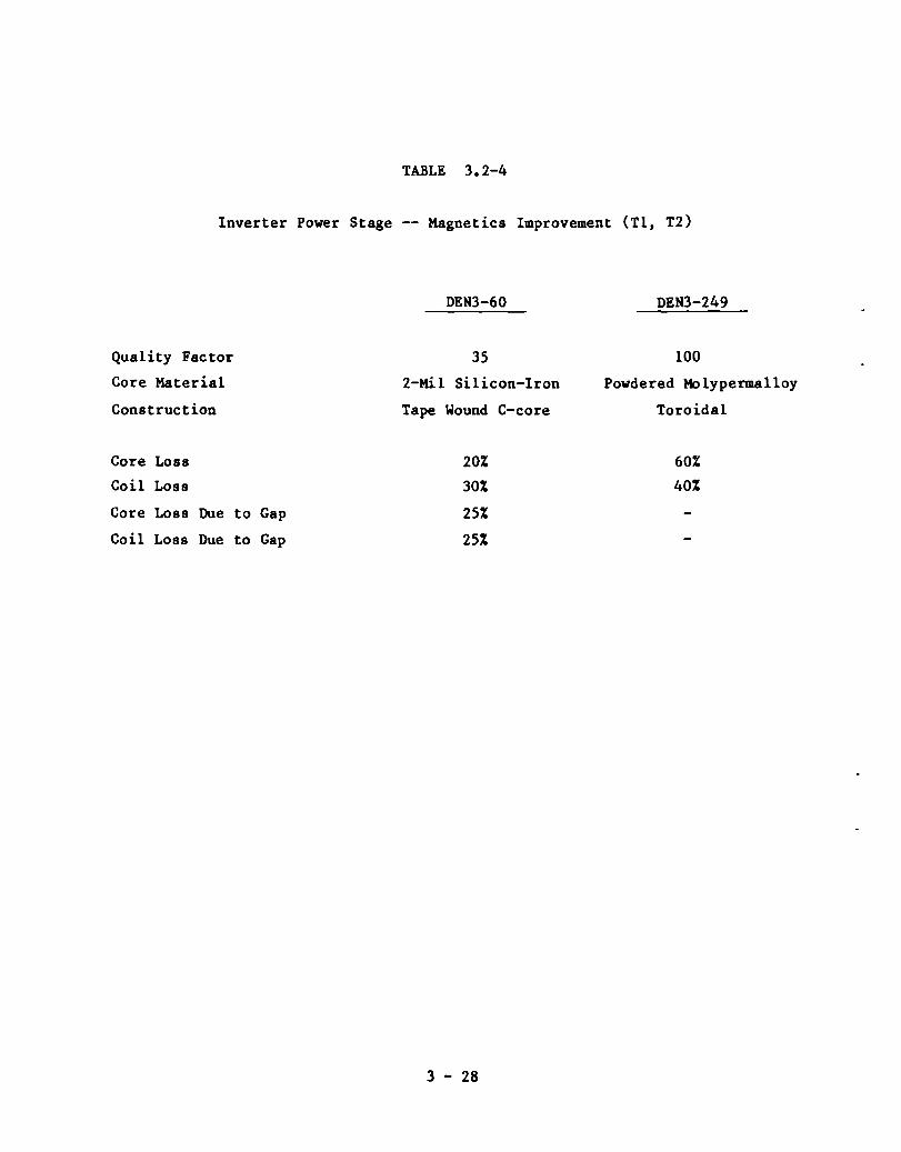
TABLE 3.2-4
Inverter Power Stage -- Magnetics Improvement (Tl, T2)
Quality Factor
Core Material
Construction
Core Loss
Coil Loss
Core Loss Due to Gap
Coil Loss Due to Gap
DEN3-60
35
2-Mil Silicon-Iron
Tape Wound C-core
20%
30%
25%
25%
3 - 28
DEN3-249
100
Powdered Molypermalloy
Toroidal
60%
40%
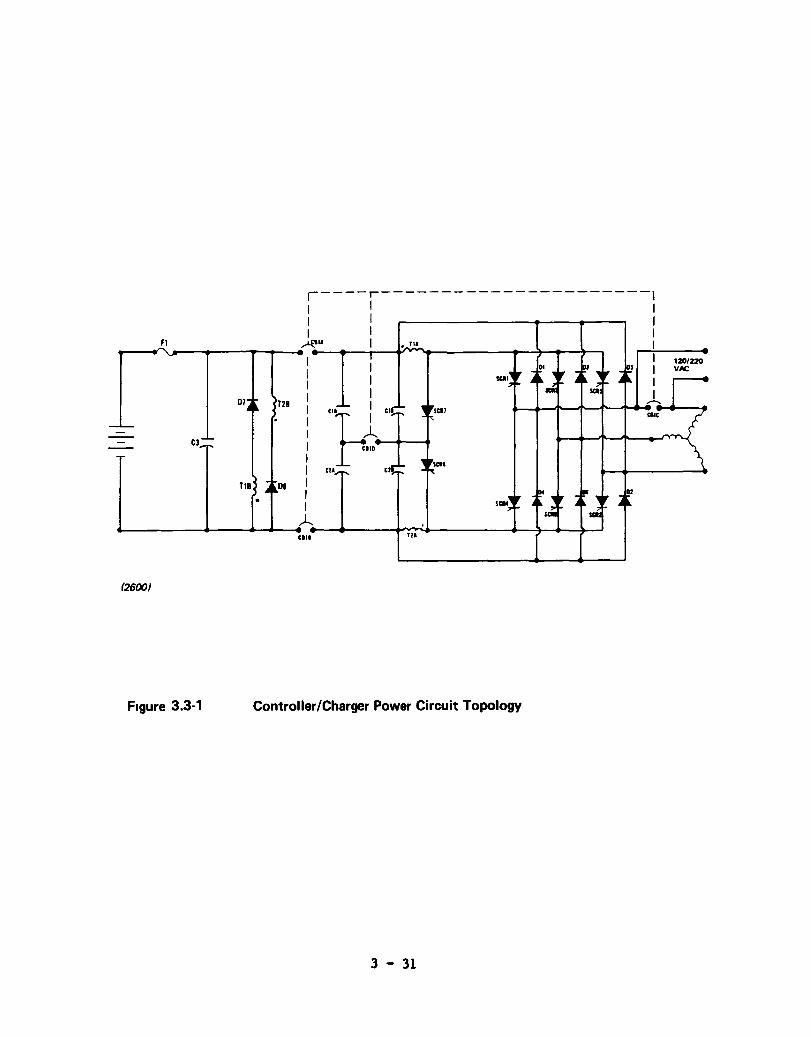
3.3 Integral Battery Charger
Operatlon of the lntegral on-board battery charger lS descrlbed and the
lnverter power stage components used to perform the battery charging function
are ldentlfled. The deslgn crlterla used to select the charger circult
parameters is presented.
The charger developed durlng thlS program provldes the features listed
ln Table 3.3-1 wlth the additlon of a four-pole clrcuit breaker to the
lnverter power stage as lliustrated in Flgure 3.3-1. Existlng semiconductors
are used to convert the ac llne voltage lnto a dc voltage suitable for
charging the propulslon battery. EXlstlng transformers, used durlng motorlng
to commutate the main lnverter thyrlstors, are used ln comblnation with the
circult breaker to lsolate the propulsion battery from the ac llne.
3.3.1 Charger Power Clrcult Operation
Charger operatlon lS descrlbed wlth the ald of Flgures 3.3-1 and 3.3-
2. Voltage is supplled to all three phases of the inverter with the ac motor
lnductance belng used to limlt the In-rush current. The main rectifiers are
used ln a brldge configuration to convert the ac line voltage to a full-wave
recti fled dc voltage whlCh appears across the ac llne fllter capacitor C4. By
operatlng the Clrcult conslstlng of TI, T2, CI, C2, SCR7 and SCRB as a
resonant converter, ln a manner similar to that used during motoring
operatlon,
propulsion
energy
battery
ln transferred from the ac line and capac1.tor C4 to the
V1.a transformer secondary windings TlB and T2B and
rectifiers 07 and 08.
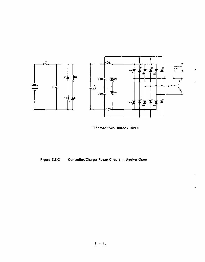
Our1.ng charger operation the circuit breaker is open to separate the
battery from the ac line. Isolation is provided via transformers Tl and T2.
Capacitor C3 is used to filter the high-frequency charging current. During
motoring operation capacitors CIA/CIB and C2A/C2B in Figure 3.3-1 are
connected 1.n parallel to provide the required commutation capacitance. During
charger operation the circuit breaker separates these capacitors to provide
the ac line filter capac1.tance, C4 (CIA and C2A in series) and the capacitance
required for charger resonant circuit operation (CIB and C2B).
3 - 29
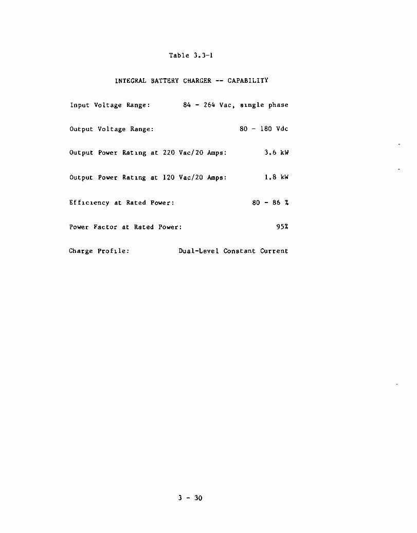
Table 3.3-1
INTEGRAL BATTERY CHARGER -- CAPABILITY
Input Voltage Range: 84 - 264 Vac. s1ngle phase
Output Voltage Range: 80 - 180 Vdc
Output Power Rat1ng at 220 Vac/20 Amps: 3.6 kW
Output Power Rat1ng at 120 Vac/20 Amps: 1.8 kW
Eff1c1ency at Rated Power: 80 - 86 %
Power Factor at Rated Power: 95%
Charge Prohle: Dual-Level Constant Current
3 - 30
fl .~
-'----- C3-.... --- " .. r-
(2600)
Figure 3.3-1
Dl~~ ~T2I .
TIB , ~ ~D' .
r----r----------------------l I I I I I I I 1 I
AliA I. '" I ,........,1:----I I I I I I I I I I I I I
I I I
c'l l.,.c_,~ ..... r"" CtA
SCIM
120/220 I V/lC
I I
~-+~~~~~~ .. ~~~~ tllC
A.-~----~~------~~~~~ TtA elll
Controller/Charger Power Circuit Topology
3 - 31
FI - . ,,. - 120/220
VI>C.
01~~ Tn C1B .
--'---- • - C3 .. r' -- C4
C2B
Ttl 01 At.' . sc ..
fl •
• C4 - (C1A + C2AI. BREAKER OPEN
Figure 3.3-2 Controller/Charger Power CirCUit - Breaker Open
3 - 32
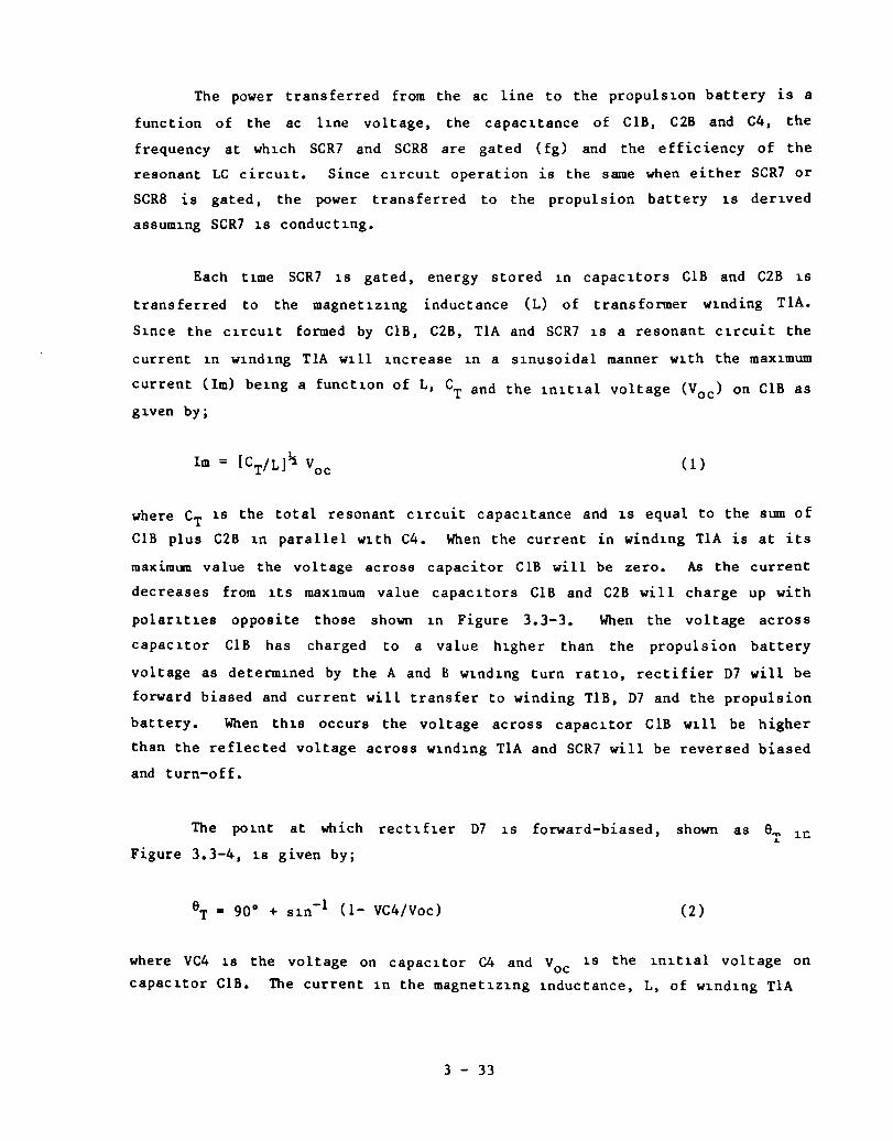
The power transferred from the ac line to the propuls10n battery is a
function of the ac 11ne voltage, the capac1tance of CIB, C2B and C4, the
frequency at wh1ch SCR7 and SCRB are gated (fg) and the efficiency of the
resonant LC circu1t. Since C1rCUl.t operation is the same when either SCR7 or
SCRB is gated, the power transferred to the propulsion battery 18 der1Ved
assum1ng SCR7 1S conduct1ng.
Each t1me SCR7 18 gated, energy stored 1n capac1tors CIB and C2B 1S
transferred to the magnet1z1ng inductance (L) of transformer w1nding TIA.
S1nce the C1rcu1t formed by CIB, C2B, TIA and SCR7 1S a resonant c1rcuit the
current 1n w1nd1ng TIA w111 1ncrease 1n a s1nu80idal manner w1th the max1mum
current (1m) be1ng a funct10n of L, CT and the 1n1t1al voltage (Voc ) on CIB as
g1ven by;
(1)
where CT 1S the total resonant c1rcuit capac1tance and 1S equal to the sum of
CIB plus C2B 1n parallel w1th C4. When the current 1n wind1ng TIA is at its
maximum value the voltage across capacitor CIB will be zero. As the current
decreases from 1tS maX1mum value capac1tors CIB and C2B will charge up with
polar1t1es opposite those shown 1n Figure 3.3-3. When the voltage across
capac1tor CIB has charged to a value h1gher than the propulsion battery
voltage as determ1ned by the A and B w1nd1ng turn rat10, rectifier 07 will be
forward biased and current will transfer to winding TIB, 07 and the propulsion
battery. When th18 occurs the voltage across capac1tor CIB w111 be higher
than the reflected voltage across w1nd1ng TIA and SCR7 will be reversed biased
and turn-off.
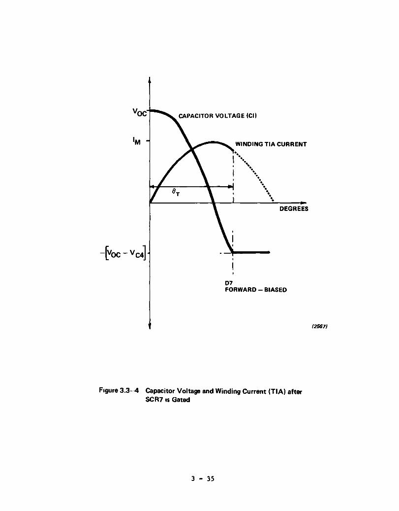
The p01nt at which rect1her 07 1S forward-biased,
Figure 3.3-4, 1S given by;
shown as e
(2 )
'I' 1G
where VC4 18 the voltage on capac1tor C4 and VOC 1S the 1n1t1al voltage on
capac1tor CIB. The current 1n the magnet1z1ng 1nductance, L, of w1nd1ng TIA
3 - 33
fl ---
-.=- + --ClA .. 1' ----
(25981
Figure 3.3-3
• TIl
07~~ ')
>. nl
C4
TIl ~~
I . 01
Charger Current Paths after SCR7 Gated
3 - 34
DI
~---- 120/220 _-,",rT""\.~ VAC
VOC CAPACITOR VOLTAGE (CI)
1M WINDING TIA CURRENT
07
•• I •••
•• . ' . ••••••
••••••• ••
DEGREES
FORWARD - BIASED
FIgure 3.3-4 Capacitor Voltage and Winding Current (TIA) after SCR7 IS Gated
3 - 35
(2567J
when rectifier D7 1S forward biased is g1ven by;
IT = Imsin aT (3)
The power available for charg1ng the propulsion battery 18 determined by the
combined frequency at which SCR7 and SCRB are gated and the angle (aT) at
which rect1fier D7 becomes forward biased as given by;
(4)
Combining equations 1, 3 and 4 the expression for the total power available
for transfer to the propulsion battery becomes,
Each thne the resonant c1rcuit 1S cycled (SCR7 or SCR8 gated) a f1xed
percentage (Kc) of the in1tial energy stored 1n the total resonant cHcuit
capacltance, CT, 1S dissipated. The power lost can be expressed as,
Subtractlng the total power lost (eq. 6) from the total power available (eq.
5) we obtaln the following expreSS10n for the charger output power.
(7)
The expression for charger efficiency is defined as;
(8 )
Substitut1ng equations [5] and [7] into equation [8] we obtain;
3 - 36
As 1S evident from equat10n [9] charger eff1c1ency 1S prunarily dependent on
the resonant C1rcu1t loss factor (Kc) and the angle (aT) at which rectifier D7
becomes forward-b1ased.
3.3.2 Circu1t Parameters
The charger c1rcuit parameters estab11shed by the inverter motor1ng
requirements are; the magnet1zing inductance of transformer w1nding TIA (L),
the total 1nverter commutat1on capacitance (Cl+C2) the battery f11ter
capacitance, C3, the transformer turns ratio (NB/NA) and the current ratings
of thyr1stors SCR7-8 and rect1f1ers D7-D8.
Flex1bility in ta11or1ng the performance of the charger was made
poss1ble using C1rcu1t breaker pole CBID shown 1n F1gure 3.3-1. This breaker
pole allowed the charger resonant C1rcu1t capac1tance to be decreased and the
thyr1stor (SCR7/8) gating frequency to be 1ncreased in order to maximize the
charger 1nput ac 11ne power factor. The charger resonant C1rcu1t capacitance
was selected based on the output power requ1red and the maximum frequency at
wh1ch thyr1stors SCR7/8 can be gated.
The max1mum gating frequency of thyr1stors SCR7/8 1S approximately
13kHz and 1S a funct10n of the transformer TIA wind1ng 1nductance, the charger
circu1t capac1tance, the time requ1red to transfer current from thyristor SCR7
to rect1fier D7, the thyristor reverse recovery t1me and the margin needed to
allow SCR7 to regain 1ts block1ng capability before thyristor SCR8 is gated
on. Charger output power at 13 kHz is shown in F1gure 3.3-5 as a function of
charger circu1t capac1tance, CT, for 120 Vac operation at low line
condit10ns. For a charger output power capabihty of 2000-2500 watts at 108
Vac the required charger c1rcuit capacitance is 1n the range of 10-13 ufo The
capacitance values selected were 8 uf for CIB and C2B and 10 uf for C4 for a
total circu1t capacitance of 12.4 ufo
To prov1de a charger output power of 3 kW at 220 Vac with a 20 amp ac
line circuit breaker the input capacitance, C4, must be small to m1nimize the
ac line reactive current. The relat10nship between power factor and input
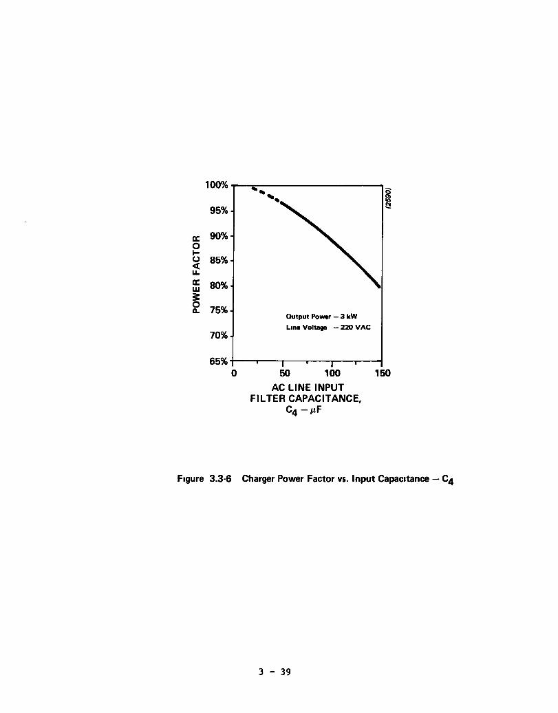
capacitance, C4, is shown 1n Figure 3.3-6. To achieve an input power factor
3 - 37
40
C'I
3.0 3: .:Jt
a: w 3: 0 2.0 Q.
~ ~ Q. ~ :J 0
1.0 KC = 0.10
0T = 1200
0.0 0 8 16 24
CHARGER CIRCUIT CAPACITANCE,
C1B + C2B I/C4, IJF
Figure 3.3-5 Charger Output Power at Maximum Gating Frequency - - - 108 VAC
3 - 38
100% Q
~ 95% '"'
a: 90% 0 .... (J 85% « u. a: 80% w 3: 0
75% a.. Output Po_r - 3 kW
LIRe Voltage - 220 VAC 70%
65% 0 50 100 150
AC LINE INPUT FIL TER CAPACITANCE,
C4 - p.F
Figure 3.3-6 Charger Power Factor VS. Input Capacitance - C4
3 - 39
greater than 90% at 220 Vac and 3 kW the Lnput capacLtance must be less than
100 ufo The Lnput lLne capacLtor must also have a hLgh nus current rating,
SLnce Lt fLlters the current pulses generated by the resonant LC circuLt, and
a voltage ratLng consLstant wLth 220 Vac operatLon (L.e. 400 volts). To
satLsfy all three requLrements the Lnverter commutatLon capacLtors were used
as Lnput capacLtors durLng charger operatLon. The capacLtance of CIA and C2A
Ln serLes 10 ufo The RMS current and peak voltage ratLng of CIA is 200 amps
and 500 volts.
3 - 40
3.4 Inverter/Charger Package
The major areas addressed to s1gm.£lcant1y reduce the package weight
and volume are 11sted 1n Table 3.4-1. M1n1m1z1ng the commutat10n circuit
losses descr1bed previously was obv10us1y 1mportant to ach1ev1ng the desired
reduct10n 1n package we1ght and volume. The use of a11-po1yprop1yene
commutation capac1tors and powdered mo1yperma110y transformer core material
resulted 1n s1gn1f1cant reduct10ns 1n the d1ssipat10n of these components w1th
the result that the 1nverter has the capab111ty to operate cont1nuous1y 1n
both s1x-step and PWM modes of operat10n. The use of forced a1r cool ing,
doub1e-s1de cooled sem1conductors (to reduce the sem1conductor Junct10n to
amb1ent-a1r thermal res1stance) and heats1nks s1zed spec1f1ca11y for each
sem1conductor were all contr1but1ng factors 1n reduc1ng the package we1ght and
volume.
3.4.1 Mechan1ca1 Descr1pt10n
The 1ntegra1 1nverter/ charger power stage package 1S shown 1n F1gure
3.4-1. The volume and we1ght of the power stage 1S .048m3 (2907) 1n3 and 47
kg 003 1bs). A compar1son of package d1menS1ons, volume and we1ght with
prev10us1y developed e1ectr1c veh1c1e 1nverter power stages 1S presented 1n
Table 3.4-2. The s1gn1f1cant reduct10n 1n we1ght and volume, espec1a11y
cons1der1ng that an 1s01ated 3.6 kw battery charger is 1nc1uded in the same
package, can be expected to d1spe1 the m1sconcept10n that thyr1stor inverters
must by nature be large and heavy. As 1nd1cated 1n Table 3.4-1 the ac
inverter/charger package 1S smaller than the dc controller developed for the
ETV-1 electric veh1c1e.
A factor 1n reducing the package volume was mounting the power
components on both s1des of a central panel. The end result 1S shown in
F1gure 3.4-2 w1th the sem1conductor dev1ces located on the bottom and the
commutat10n components, £l1ter capac1tors and C1rcu1t breaker located on the
top of this central panel. This approach prov1ded two advantages; 1) 1t
allowed the a1r-flow through the semiconductor heats1nks to be max1m1zed by
baff11ng the a1r flow through the top half of the package and 2) 1t m1n1mized
the package paras1t1c inductances.
3 - 41
TABLE 3.4-1
Areas Addressed to Reduce Package Volume
Component Losses Reduced
Double-side Cooled Semiconductors Used
Forced Air-cooling
Heatsinks Sized Specifically for Each Device
Two-level Package Design
Table 3.4-2
Inverter Power Stage Package Comparison
Vol m2 (in3) Weight kg (1bs) Dimensions cm (in)
Gould (DEN3-60) .087 (5292) 61
GE (DEN3-59) .130 (904) 59
Eaton (DEN3-125) .083 (5040) 60
GE (ETV-1, de) t .052 (3168) 43
Gould (DEN3-249)* .048 (2907) 47
t Includes non-isolated 2.5 kW battery charger
* Includes Isolated 3.6 kW Battery Charger
3 - 42
(135) 7lx53x23 (28x2lx9)
(130) 96x66x20 (38x26x8)
(131) 7lxSlx23 (28x20x9)
(95) S6x41x23 (22x16x9)
(103) 48x43x23 (l9x17x9)
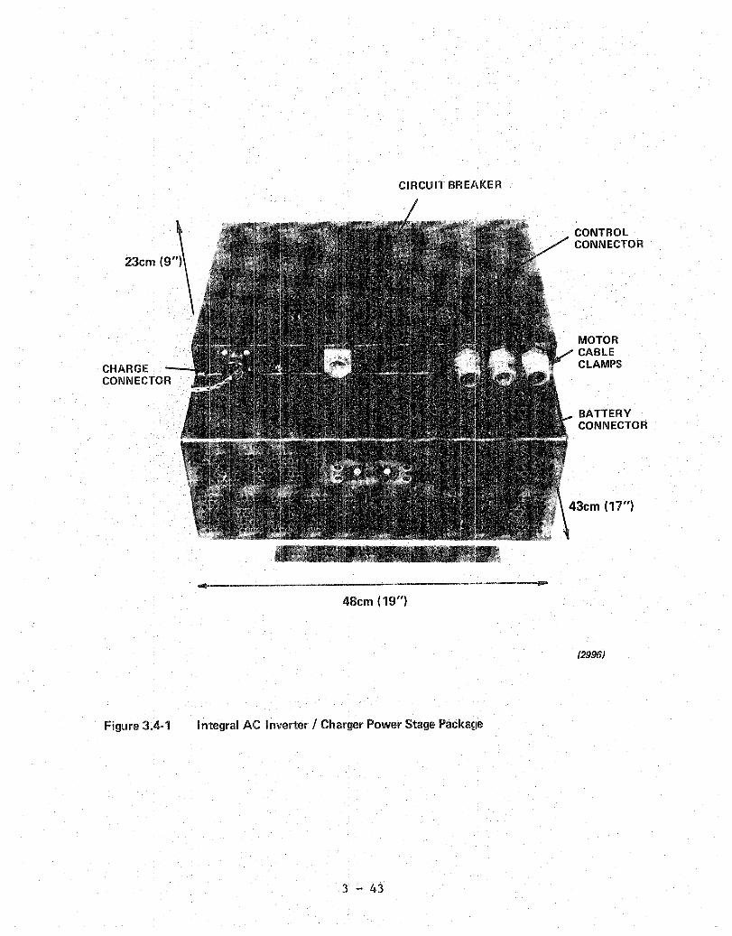
CHARGE CONNECTOR
Figure 3.4·1
CIRCUIT BREAKER
-------.-----------.----------48cm (19")
Integral AC Inverter / Charger Power Stage Packa~le
3 - 43
CONTROL CONNECTOR
MOTOR CABLE CLAMPS
BATTERY CONNECTOR
(2996)
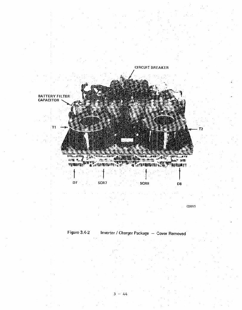
CIRCUIT BREAKER
12
D7 SCR7 SCRS D8
(2991)
Figure 3.4-2 Inverter / Charger Package - Cover Removed
3 - 44
3.4.2 Package Weight and Volume
The welght of the lndlvldual components and assemblles used in the
inverter/charger power stage are hsted 1.n Table 3.4-3. Included with the
1.nverter/ charger package 1.S a removable fan assembly, wh1.ch has been slzed
speclflcally for dynamometer testlng. Utlllzing vehlcle ram air would
slgnificantly reduce the welght and volume of the fan assembly.
The ma1.n thyrlstors (SCRl-6) requlre the largest heatsinks as a result
of the lnverter peak and steady-state power requlrements. The main rectlfier
heatsink assembly 15 40% smaller as theu average disSlpation 15 lower and
thelr maximum Junctlon temperature 15 higher than the maln thyristors (175°C
versus 125°C). In a slmlllar fashion the d1.SS1pat1.0n of the commutation
thyrlStors (SCR7-8) lS greater than the energy recovery rectlhers. The
weight dlStributlon of the power stage components by functlon 15 shown in
Flgure 3.4-4. As expected the commutatlon components account for the largest
percentage ~37%) of the power stage weight.
3 - 45
TABLE 3.4-3
Inverter/Charger Component Weights
Ma1n Thyr1stor Assy (SCRl-6)
Ma1n Rect1f1er Assy (Dl-6)
Com Thyr1stor Assy (SCR7-8)
Clamp Rect1her Assy (D7-8)
Cornmutat10n Transformers (Tl-2)
Commutat1on Capac1tors (Cl-2)
C1rcu1t Breaker
Battery F11ter Capac1tors (C3)
Enclosure Alum1num Panels
Component Mount1ng Panel
Bus Bars
Cable
Current Transducer
Gate Dr1ve & Snubber PCB's
Battery Shunt/Fuses
M1SC (Control Cable, Connectors, Hardware, Etc.)
Total (Inverter/Charger)
Fans
Fan dc/dc Converter
Mount1ng Panel
Total (Fan Assembly)
3 - 46
~
5876
3516
1906
1146
9734
4568
2937
2826
4911
2703
2198
667
1024
612
575
1569
46762
2024
817
575
3416
lbs
(13)
(8)
(4)
(3)
(22)
(10)
(6)
(6 )
(11)
(6 )
(5)
(1)
(2)
(1)
(1)
(4 )
(103 Ibs)
(4 )
(2)
(1)
(7.5 lbs)
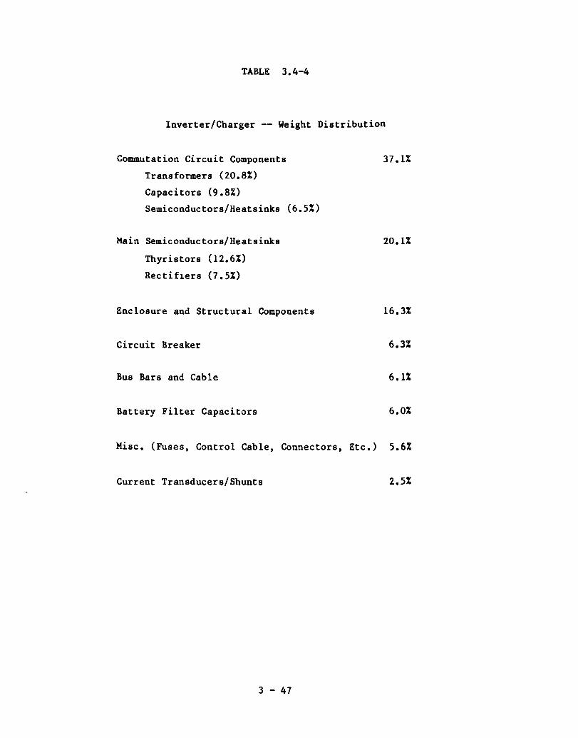
TABLE 3.4-4
Inverter/Charger -- Weight Distribution
Commutation Circuit Components
Transformers (20.8%)
Capacitors (9.8%)
Semiconductors/Heatsinks (6.5%)
Main Semiconductors/Heatsinks
Thyristors (12.6%)
RectifLers (7.5%)
37.1%
20.1%
Enclosure and Structural Components 16.3%
Circuit Breaker 6.3%
Bus Bars and Cable 6.1%
Battery Filter Capacitors 6.0%
Misc. (Fuses, Control Cable, Connectors, Etc.) 5.6%
Current Transducers/Shunts 2.5%
3 - 47
4. TEST AND EVALUATION
4.1 Charger Operat10n
Operation of the 1ntegral on-board battery charger is descr1bed with
eff1ciency. power factor and charge prof1le test results presented.
Operat10n of the on-board charger requ1res connect1ng the charge cable
from the ac hne 1nterface un1t to the power stage and placing the keyswitch
1n the charge pos1t10n. The charge control electron1cs will automatically
move the power stage c1rcuit breaker to the charge position. close the ac l1ne
contactor located 1n the interface unit and after a 10 second time delay
act1vate the charger. The 1n1t1al battery charge current will be selected
automat1caUy depend1ng on the ac lLne voltage applLed to the charger. For
example. the 1n1tial charge current w1ll be 10 amps at 120 vac and 20 amps at
220 vac.
4.1.1 120 Vac Operation
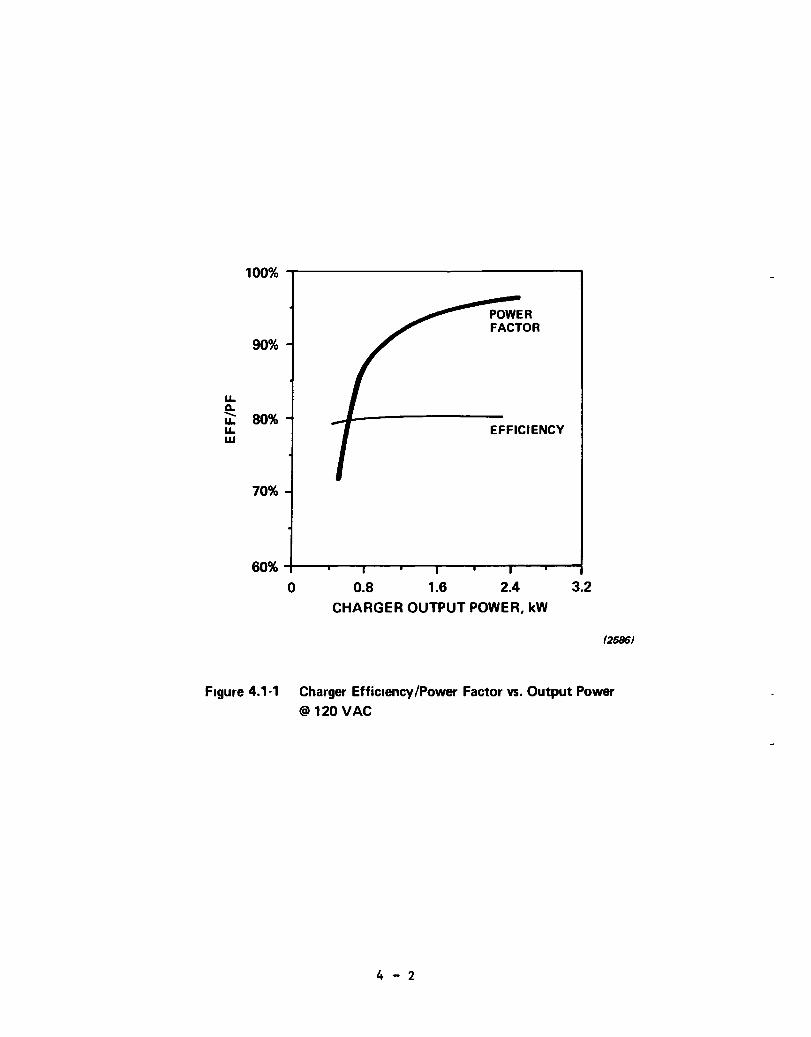
Measured charger eff1c1ency and power factor as a funct10n of charger
output power 18 presented 1n F1gure 4.1-1 for 120 Vac operat10n. As shown.
charger efhc1ency is constant at approx1mately 80% over a wide output power
range. Charger power factor at 120 Vac and rated output power(l.8kW) is in
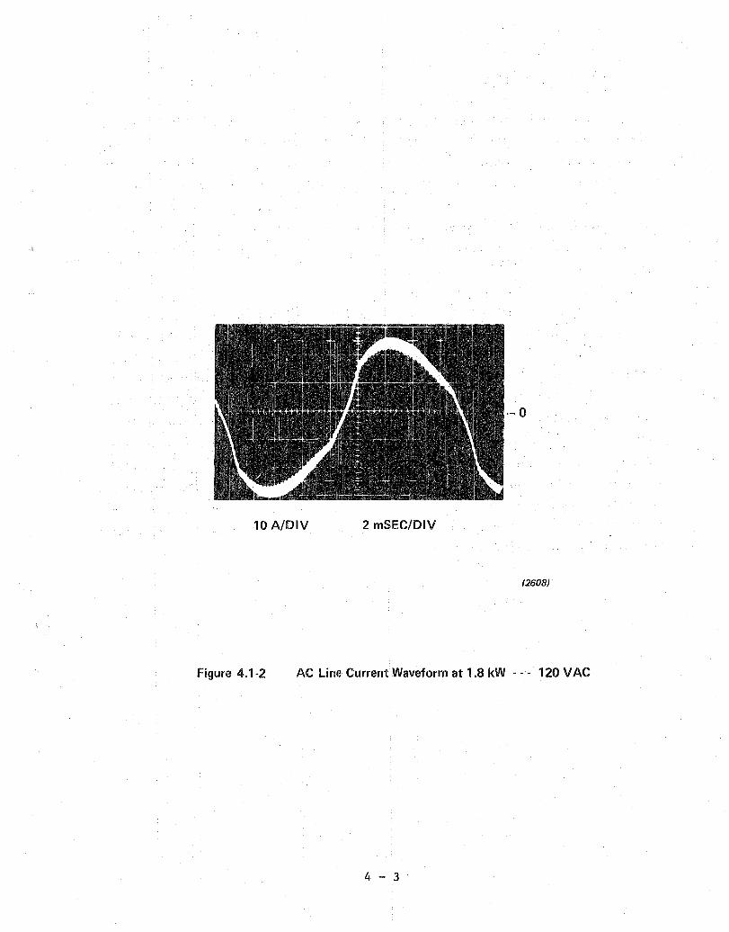
the range of 95%. The input ac line current waveform at 120 Vac and an output
power of 1.8 kW 1S shown in Figure 4.1-2. The total harmonic distortion of
the current waveform shown in Figure 4.1-2 is 12%.
4 - 1
U. Q.
100% ~----------------------------~
90%
u.: 80% u. w
EFFICIENCY
70%
60% +--"T"""'"""---,----r-"""'T"'"-""T"'""'-r----,.-......
o 0.8 1.6 2.4 3.2 CHARGER OUTPUT POWER, kW
(2586)
Figure 4.1-1 Charger Efficiency/Power Factor YS. Output Power @ 120 VAC
4 - 2
.- 0
10 A/DIV 2 mSEC/DIV
(2608)
Figlure 4.1-2 AC Line Current Waveform at 1.8 kW - - - 120 V AC
4 - 3
4.1.2 220 Vac Operation
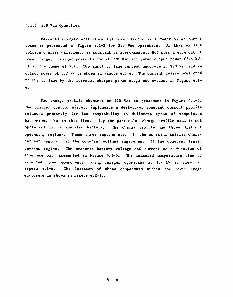
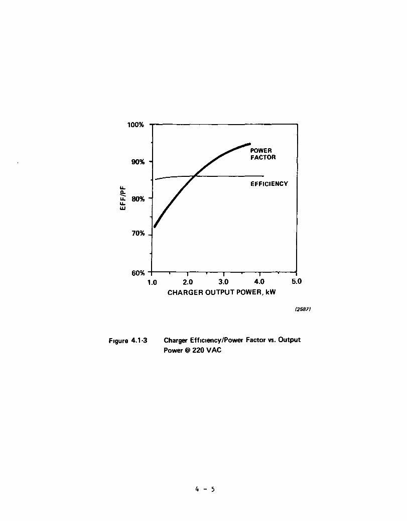
Measured charger efficiency and power factor as a function of output
power u presented 1n F1gure 4.1-3 for 220 Vac operation. At th1S ac line
voltage charger eff1ciency 1S constant at approx1mately 86% over a wide output
power range. Charger power factor at 220 Vac and rated output power (3.6 kW)
1S 1n the range of 95%. The 1nput ac line current waveform at 220 Vac and an
output power of 3.7 kW 1S shown in Figure 4.1-4. The current pulses presented
to the ac llne by the resonant charger power stage are evident in Figure 4.1-
4.
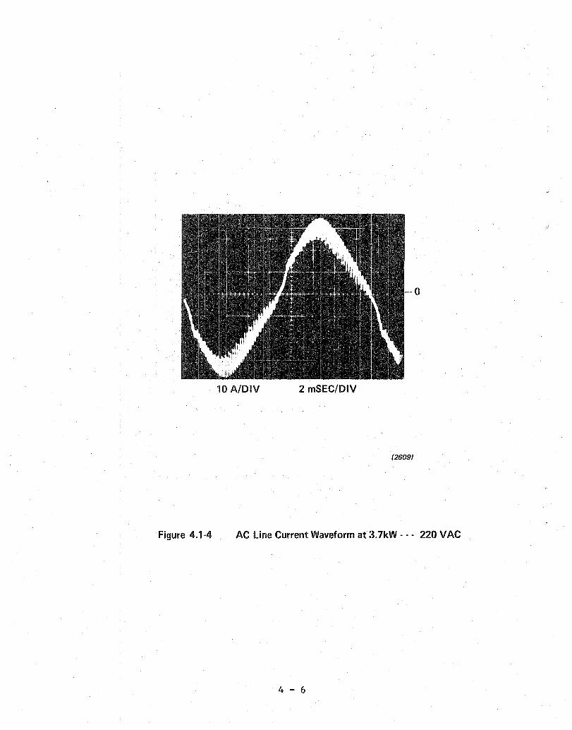
The charge proflle obta1ned at 220 Vac is presented in Figure 4.1-5.
The charger control circuit implements a dual-level constant current profile
selected pr1mar1ly for its adaptab1lity to different types of propuls1on
batter1es. Dut to th1S flex1b1lity the part1cular charge profile used is not
opt1m1zed for a speciflc battery. The charge profile has three distinct
operat1ng regions. These three regions are; 1) the constant initial charge
current reg1on, 2) the constant voltage region and 3) the constant finish
current region. The measured battery voltage and current as a function of
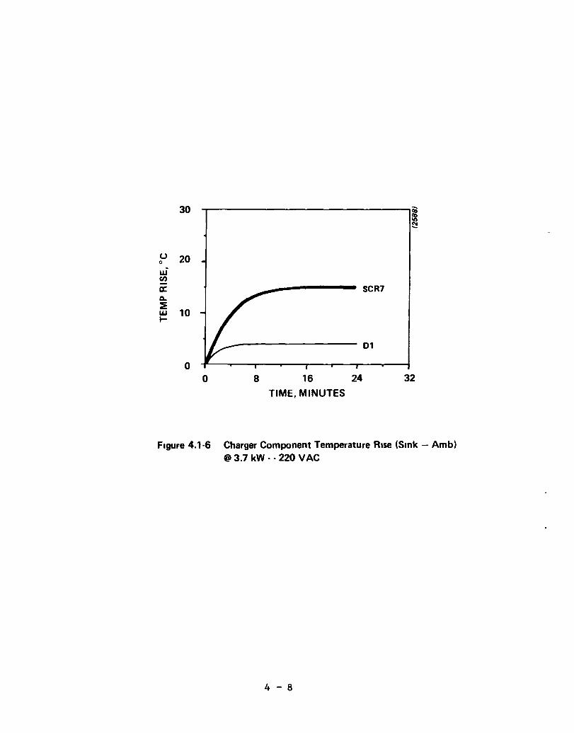
t1me are both presented in Figure 4.1-5. The measured temperature rise of
selected power components during charger operation at 3.7 kW is shown in
Figure 4.1-6. The locat1on of these components within the power stage
enclosure is shown in Figure 4.2-15.
4 - 4
100%
POWER
90% FACTOR
LL EFFICIENCY
a. - 80% LL LL w
70%
60% +--~-r-----'r----r---.--......---...-----I
1.0
Figure 4.1·3
2.0 3.0 4.0 5.0 CHARGER OUTPUT POWER, kW
(2587)
Charger Efficiency/Power Factor vs. Output
Power @ 220 VAC
4 - 5
o
10 A/DIV 2 mSEC/DIV
(2609)
Figure 4.1-4 AC line Current Waveform at :3.7kW - - - 220 VAC
4 - 6
VBAT 'sAT
180 28
170 24
160 20 "sAT
150 16
140 12
130 8
120 4 IBAT
110 0
0 2 4 6 8 10
CHARGE TIME, HOURS
Figure 4.1-5 Charge Profile at 220 VAC - - - Nominal 132 Volt Battery (80% 000)
4 - 7
30 I u 20 0
w CI)
~ SCR7 Q.
~ w t-
10
01
0 0 8 16 24 32
TIME, MINUTES
Figure 4.1·6 Charger Component Temperature Rise (Smk - Amb) @3.7 kW·· 220 VAC
4 - 8
4.2 Inverter Operation
Inverter operation requires that the keyswitch be moved to the off
position, the charge cable be disconnected from the power stage, the power
stage circuit breaker be moved manually to the motoring position and the
keyswitch be moved to the motor position.
After the key switch is moved to the motor position the commutation
c~rcuit w~ll cycle to charge the commutation capacitors to the required
voltage level and the motoring status lights on the control electronics
enclosure will light momentarily. Moving the direction selector to either the
forward (FWD) or reverse (REV) posit~on and rotating the accelerator control
knob will activate the main thyristors and initiate motoring operation.
4.2.1 Power Loss/Efficiency Data
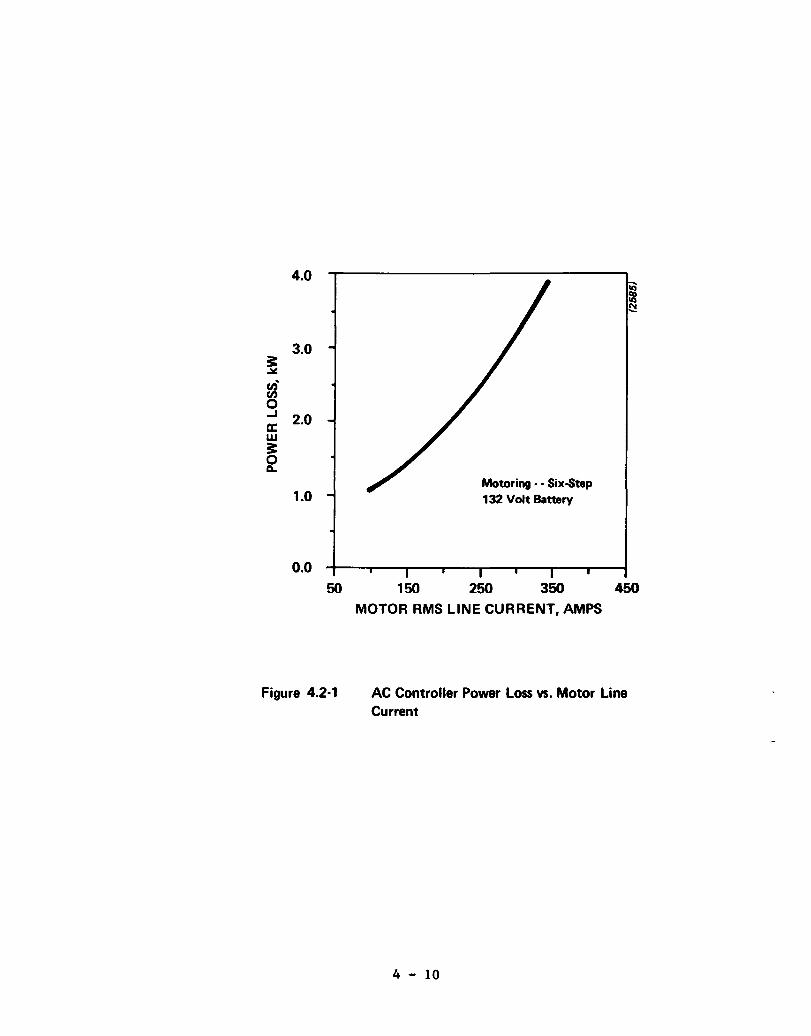
Measured inverter power loss during six-step motoring operation is
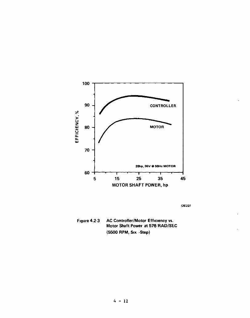
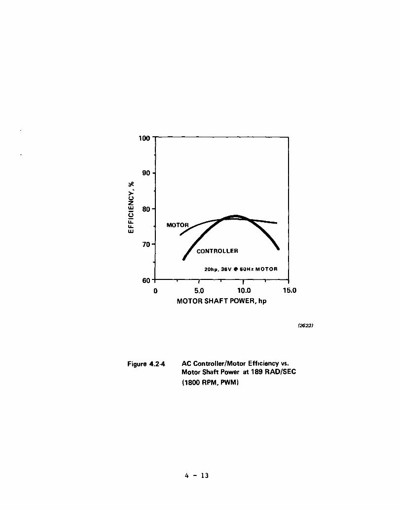
presented in Figure 4.2-1 as a function of motor RMS line current. The
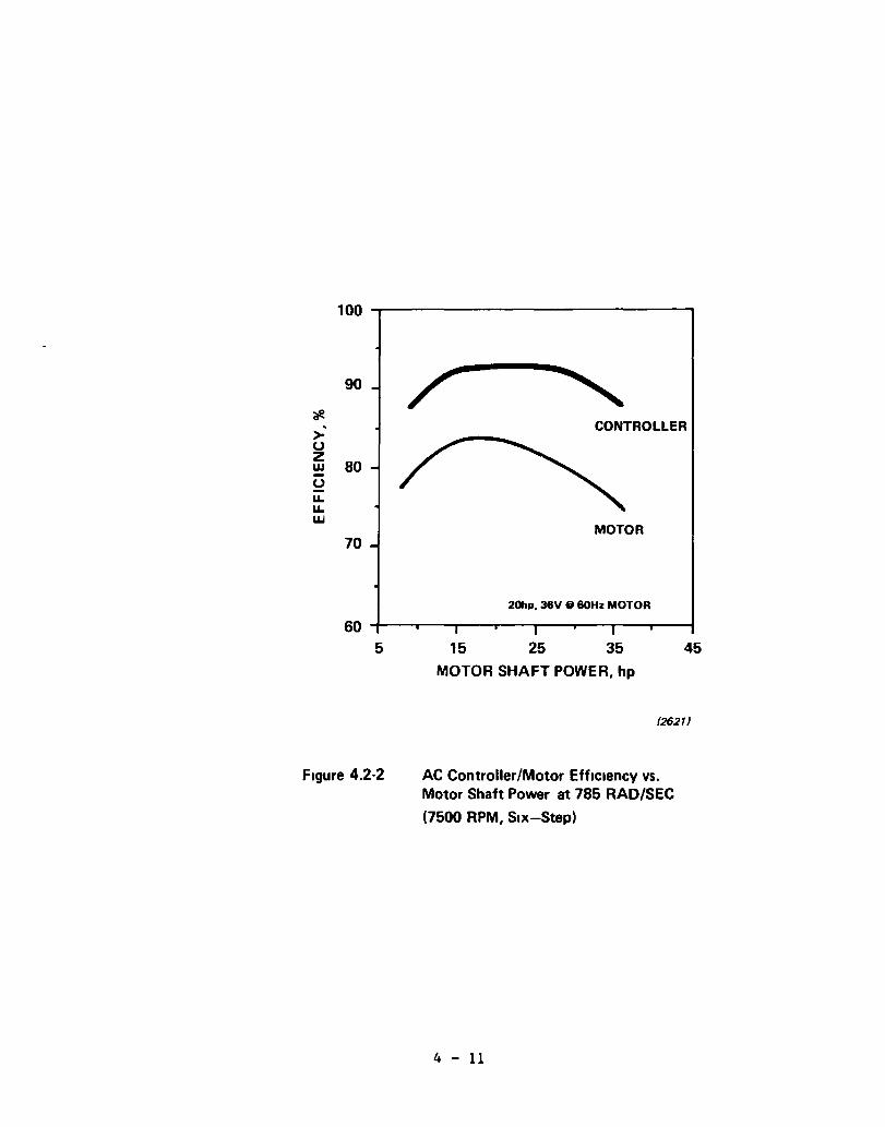
measured inverter and motor efhciency (20 hp ac induction motor) at motor
shaft speeds of 785 rad/sec (7500 RPM), 576 rad/sec (5500 RPM) and 189 rad/sec
(1800 RPM) is presented 10 Figures 4.2-2, 3 and 4 respectively. Motoring
operation at 189 rad/sec (1800 RPM) corresponds to operation in the pulse
width-modu1ation (PWM) region wh~ch occurs at motor speeds below approximately
471-524 rad/sec (4500-5000 RPM) depending on load. PWM operation is
characterized by an ~ncrease in commutation frequency to decrease the time the
main thyristors are on and the applied motor voltage. The motor line current
during PWM operat~on at 189 rad/ sec (1800 RPM) and 10 hp is shown in Figure
4.2-5.
4 - 9
4.0
3.0 3: ~
~' o ...J a:: 2.0 w 3: ~
1.0
0.0 50
Figure 4.2-1
150
Motoring· . Six..step 132 Volt Battery
250 350
MOTOR RMS LINE CURRENT, AMPS
450
AC Controller Power Loss vs. Motor Line Current
4 - 10
100 ~----------------------------~
90
crP.
> Co) z w 80 Co)
LL. LL. w
70
5
Figure 4.2·2
CONTROLLER
MOTOR
2Ohp. 36V .. 60Hz MOTOR
15 25 35 45
MOTOR SHAFT POWER, hp
(2621)
AC Controller/Motor Efficiency vs. Motor Shaft Power at 785 RAD/SEC
(7500 RPM, Six-Step)
4 - 11
100
~ ....
90 CONTROLLER
;i!.
> U Z w 80 MOTOR U u.. u.. w
70
2Ohp, 36V • 50Hz MOTOR
5 15 25 35 45
MOTOR SHAFT POWER, hp
(2622)
Figure 4.2-3 AC Controller/Motor EffIciency vs. Motor Shaft Power at 576 RAD/SEC
(5500 RPM, SIX -Step)
4 - 12
100~--------------------------
90
ae. > (,) Z w 80 (,)
u.. u.. w
70
20hp. 36V • 60Hz MOTOR
60+---~----~--~--~~--~--~
o 5.0 10.0 15.0
MOTOR SHAFT POWER, hp
Figure 4.2-4 AC Controller/Motor EffIciency vs. Motor Shaft Power at 189 RAD/SEC
(1800 RPM, PWM)
4 - 13
(2623J
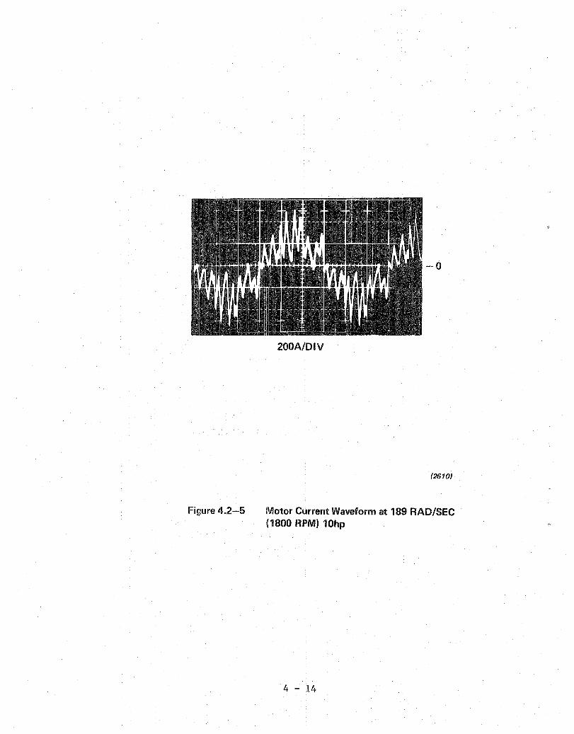
Figlure 4.2-5
-0
200A/DIV
(2610)
Motor Current Waveform at 189 RAD/SEC (1800 RPM) 10hp
4 - 14
4.2.2 Power Loss Breakdown
An important step in reducing the l.nverter power stage weight and
volume was obtaining a reliable estimate of the inverter losses. Thl.S was
accompll.shed uSlng a computer model of the inverter, motor and propulsion
battery that allowed l.nverter losses to be determined under different steady
state operatl.ng condl.tl.ons. The model utilized the ac induction motor
equivalent Cl.rcul.t shown in Figure 4.2-6. The motor parameters shown in
Fl.gure 4.2-6 are the stator (Rl) and rotor (R2) resl.Stance, the stator (xl)
and rotor (X2) leakage reactance, the magnetizing reactance (Xm) and the iron
and stray load losses (Rc). Information on how the above motor parameters
vary as a function of motor operatl.ng condl.tions was obtained from Gould's
Electric Motor Dl.vision. This information included magnetizing inductance as
a function of motor voltage, stator and rotor leakage reactance as a function
of current and frequency, iron losses as a function of voltage and frequency
and stray load losses as a functlon of voltage, frequency and rotor current.
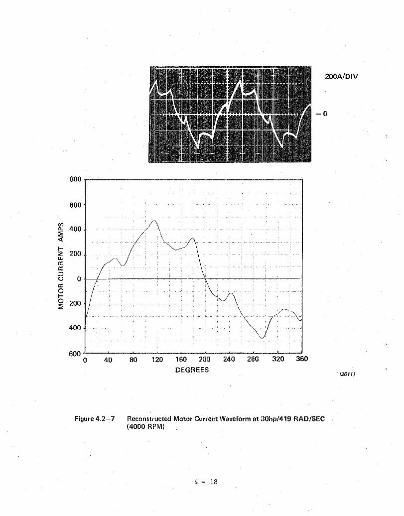
Inverter losses were calculated by performing a fourier analysis of the
l.nverter output voltage waveform to determine the fundamental and harmonic
voltages applied to the motor. The motor equivalent circuit was determined at
the fundamental and harmonl.c frequencies and used in combination with the
l.nverter harmonic voltages to produce a representation of the motor line
current. The reconstructed and actual motor ll.ne current are presented in
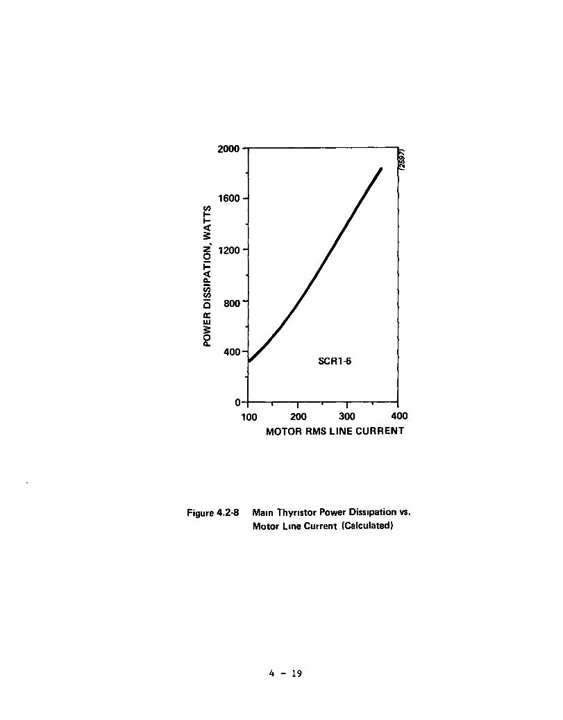
Fl.gure 4.2-7 for comparison. The main thyristor losses were calculated using
the reconstructed motor line current waveform by numerically integrating the
produc t of the motor hne current and l.nstantaneous thyristor voltage drop
between 0 and 180 electrical degrees. The calculated main thyristor (SCRl-6)
power dissipation as a function of motor RMS line current is presented in
Fl.gure 4.2-8 for motorlng operation at 576 rad/sec (5500 RPM).
The commutatl.on thyrl.stor power dl.ssipatl.on was calculated using the
peak motor ll.ne current obtal.ned from the reconstructed motor line current
waveform. The calculated thyristor losses l.nclude both turn-on and conduction
losses. The power dl.ssipation of the commutation thyristors (SCR7-8) is
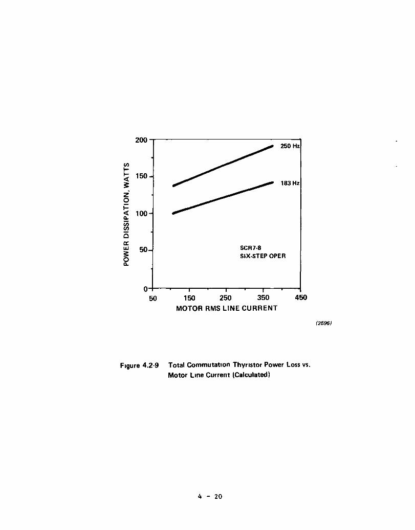
shown in Flgure 4.2-9 as a function of motor RMS line current and frequency.
4 - 15
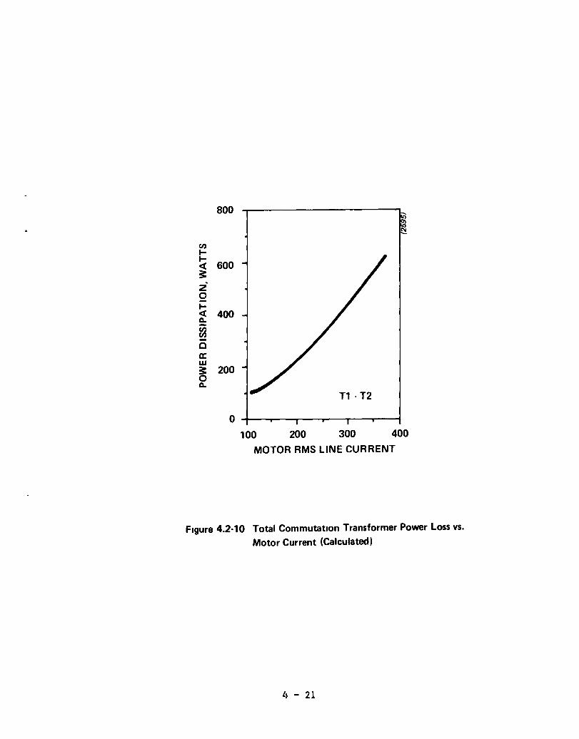
The losses of the commutation transformers were calculated based on the core
loss data obtained uSing the resonant frequency test procedure. The total
transfonner losses are presented in Figure 4.2-10 and were based on the
calculated RMS current in the TlA and TlB windings, the measured resistance of
these windings and the core loss data. The significant increase in
transformer losses at higher current levels is a result of the TlA winding
being in series With the load. A breakdown of inverter losses at 576 rad/sec
(5500 RPM) for motor shaft power levels of 15 and 45 hp is presented in Table
4.2-1.
4 - 16
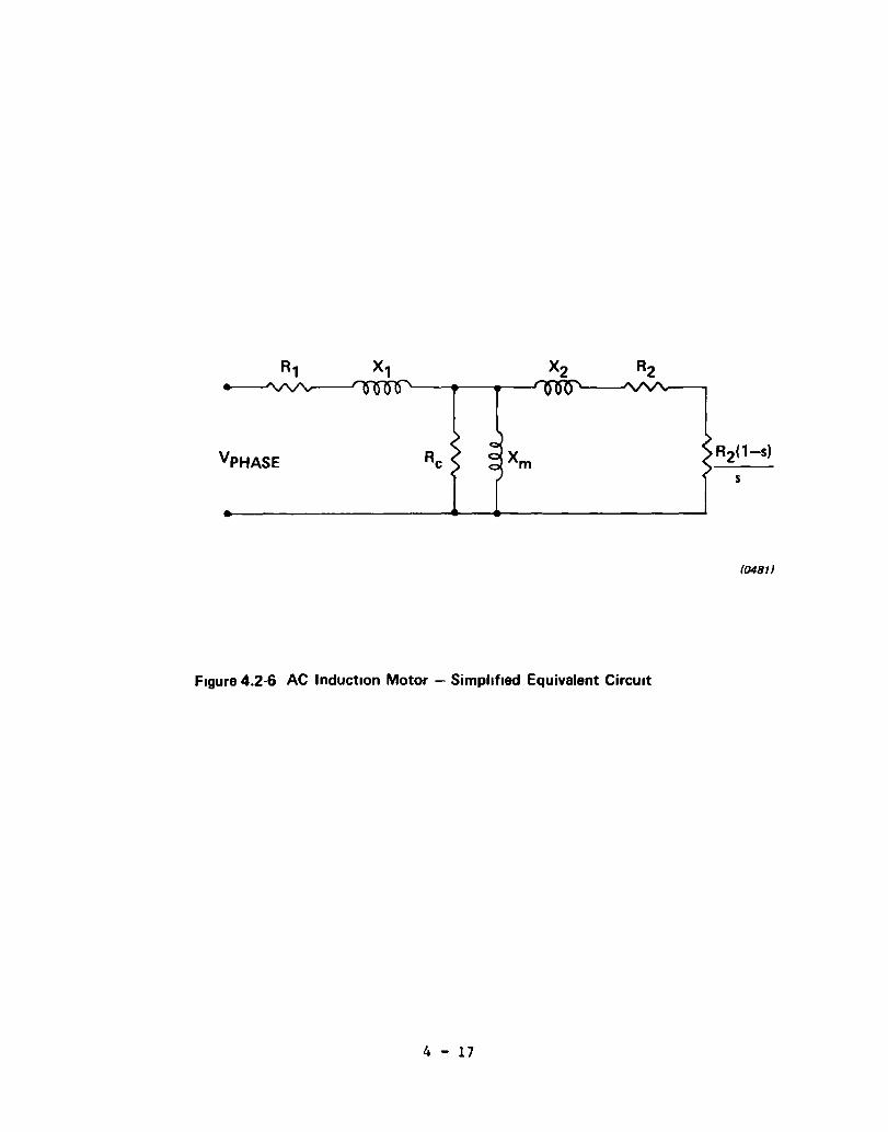
(0481)
Figure 4.2-6 AC Induction Motor - Simplified Equivalent Circuit
4 - 17
200A/DIV
-0
800.,-------,
600 ... ---...1.'-----'---1 _ ......... _, --......... ---'--...... ......&-.-,-""'""'-----o 40 80 120 160 200 240 280 320 360
DEGREES
Figure 4.2-7 Reconstructed Motor Current Waveform at :~Ohp/419 RAD/SEC (4000 RPM)
4 - 18
(2611)
2000 '" C'J
1600 en ~ ~ « 3: , z 1200 0 i= « Q.
en en C 800 a: w 3: 0 Q.
400 SCR1-6
100 200 300 400
MOTOR RMS LINE CURRENT
Figure 4.2-8 Mam ThYrIStor Power DiSSipation vs. Motor Lme Current (Calculated)
4 - 19
200 250 Hz
(I)
~ ~ 150 ~ 3: 183Hz
Z 0 ~ ~ 100 ~
(I) (I)
c a: w 50 SCR7·8 3: SIX·STEP OPER 0 ~
50 150 250 350 450
MOTOR RMS LINE CURRENT
(2596)
Figure 4.2·9 Total Commutation ThYristor Power Loss vs.
Motor Line Current (Calculated)
4 - 20
800
en ~ ~
600 ~ ~
Z 0 ~ ~ 400 Q.
~ C a:: w ~ 200 0 Q.
Tl - T2
0
100 200 300 400
MOTOR RMS LINE CURRENT
Figure 4.2-10 Total Commutation Transformer Power Loss vs.
Motor Current (Calculated)
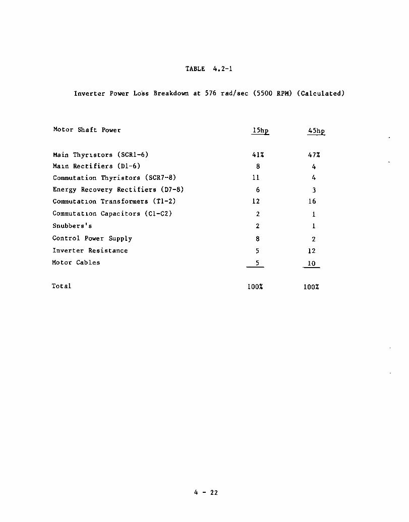
TABLE 4.2-1
Inverter Power Loss Breakdown at 576 rad/sec (5500 RPM) (Calculated)
Motor Shaft Power
Main Thyr~stors (SCRl-6)
Ma~n Rectifiers (Dl-6)
Commutation Thyristors (SCR7-8)
Energy Recovery Rectifiers (D7-8)
Commutat~on Transformers (Tl-2)
Commutat~on Capacitors (C1-C2)
Snubbers's
Control Power Supply
Inverter Resistance
Motor Cables
Total
4 - 22
41%
8
11
6
12
2
2
8
5
5
100%
47%
4
4
3
16
1
1
2
12
10
100%
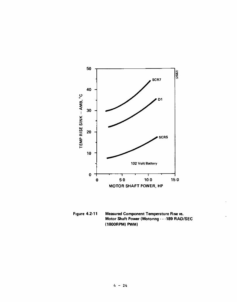
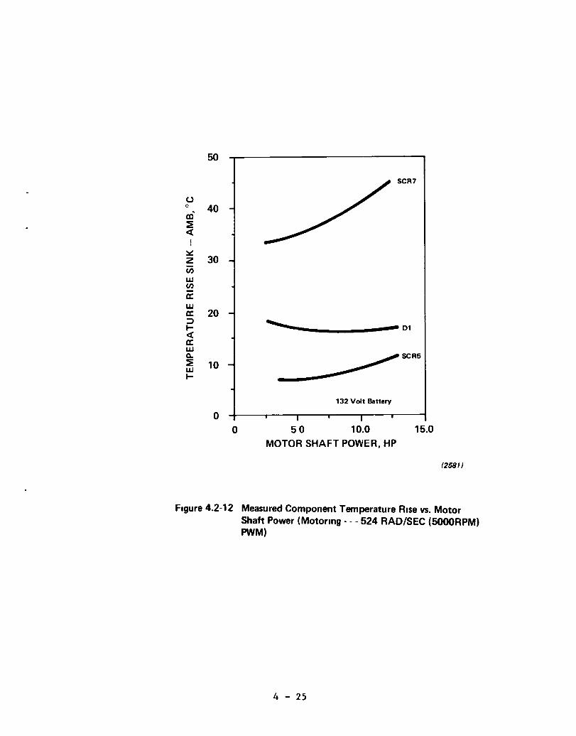
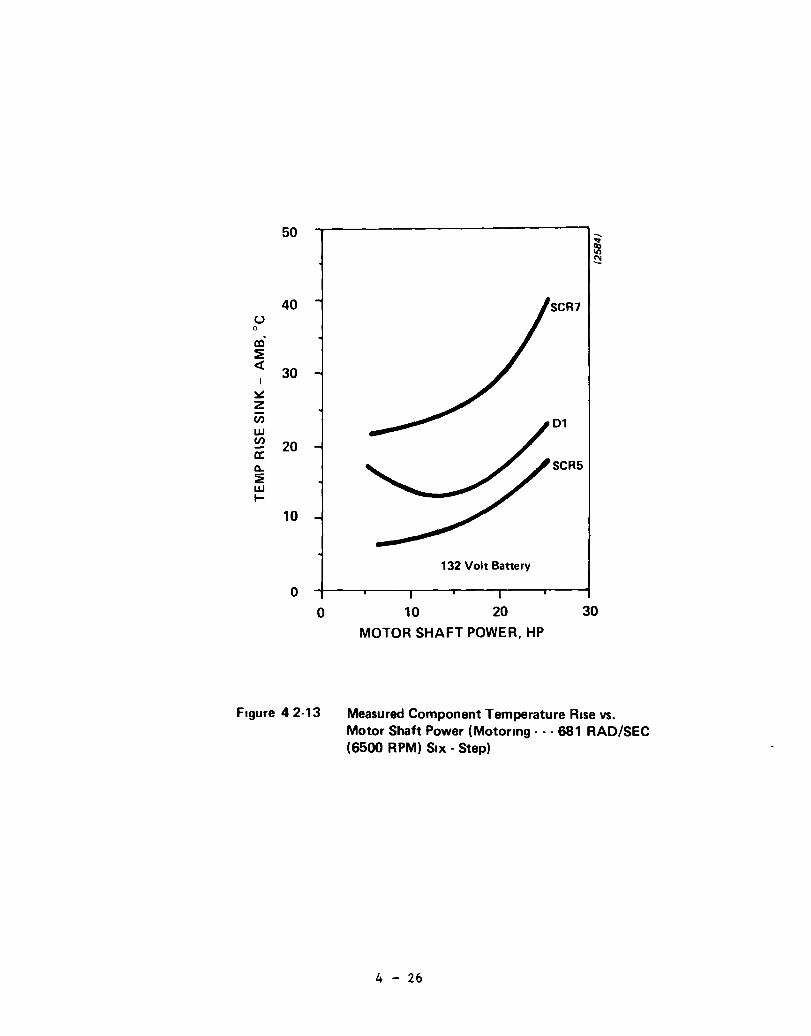
4.2.3 Component Temperature Rise
The measured temperature rise of selected power stage components is
presented ~n Figures 4.2-11, 12 and 13 for motoring operation at shaft speeds
of 189 rad/sec (1800), S24 rad/sec (SOOO) and 681 rad/sec (6S00 RPM).
Component temperature rlSe during regenerat~on at 681 rad/sec (6S00 RPM) is
presented ~n F~gure 4.2-14. The specific components monitored were main
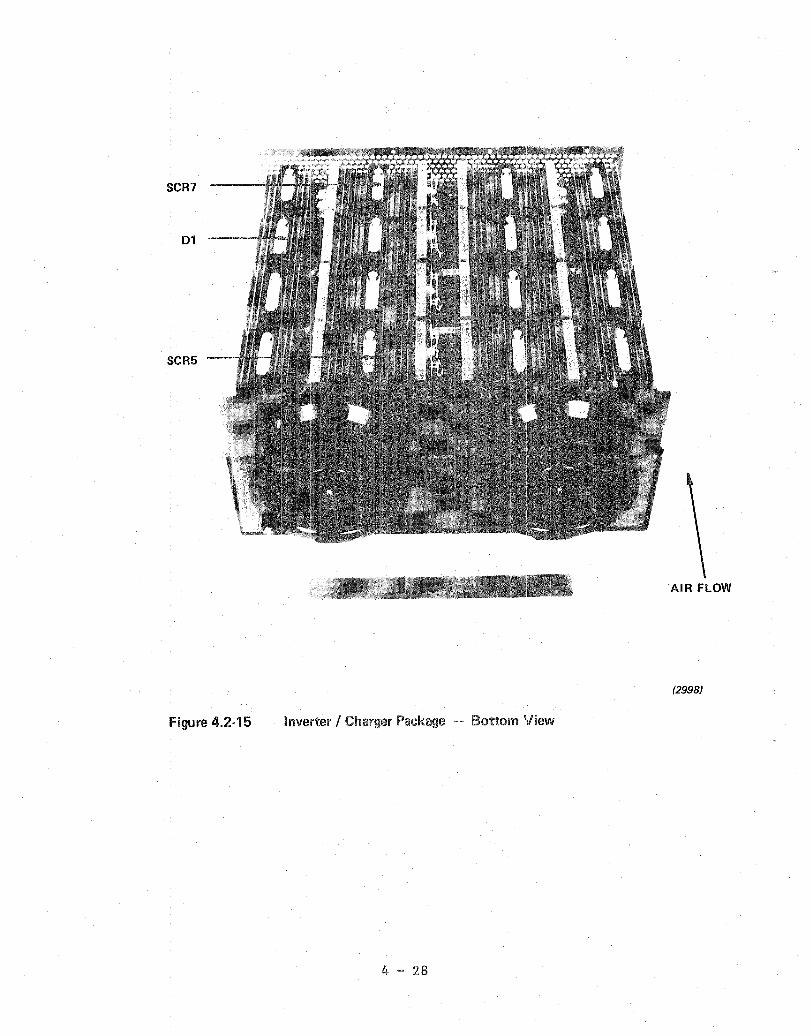
thyristor SCRS, ma~n rect~fier D1 and commutation thyristor SCR7. The
location of these components within the power stage enclosure is shown in
F~gure 4.2-1S. A~r flow direction through the package is indicated in Figure
4.2-1S. S~nce thyristor SCR7 is located at the outlet it will operate at a
higher ambient temperature than main thyristor SCRS. As is evident the main
rectifier heatS1nks are significantly smaller than the main thyristor heat
sinks to take advantage of their lower d~ssipation during motoring operation
and their higher junction temperature rating.
The inverter steady-state power rat~ng is 11.2 kW (lShp). As indicated
~n F~gure 4.2-13 the temperature rise of thyrlStor SCRS is only 9°C at this
power level. During an acce1erat~on from 40-88.S km/h (2S-SS mph) at 33.6 kW
(45hp), however, the ma~n thyristor d~ssipation ~s approximately 300 watts and
the Junct~on temperature must remain below 12SoC at this operating point. For
a Junction to heats~nk thermal res~stance of 0.13 °C/W (GE C384), a 10°C rise
~n a1r temperature above ambient (SCR1) and an ambient temperature of 49°C the
1n~tta1 Junct10n temperature of thyristor SCR1 at 4Shp will be 107°C. The
18°C difference between the 1nitia1 and max~mum junction temperature is
ava~lab1e for transient operat1on (~.e., 16 seconds at 4Shp).
Dur1ng PWM operation at S24 rad/sec (SOOO RPM) the commutation circu~t
~s operating at its maximum motoring frequency (i.e., approximately lS00
commutations per thyristor) and the diss~pation of thyristor SCR7 is at its
max~mum value. For th~s operating condition the heatsink to ambient
temperature rise of thyristor SCR7 is approximately 40°C as shown in Figure
4.2-12. At an ambient temperature of 49°C the Junction temperature ~s
aproximate1y 11SoC and 1S below the max~mum junction temperature of 12SoC. At
the above PWM operat~ng pomt (i.e., 7.S kW (lOhp) @ S24 rad/sec (SOOO RPM»
the temperature rise of the commutation transformer winding was 46°C and the
temperature rise of the commutation capacitor case (C1) was only SoC.
4 - 23
50
40
0 0
eel ~ ~ 30
~ z CI)
w en 20 a: Q. ~ W ~
10
0 0
Figure 4.2-11
~ SCR7
~
01
SCR5
132 Volt Battery
50 100 150
MOTOR SHAFT POWER, HP
Measured Component Temperature Rise vs. Motor Shaft Power (MotormQ - - -189 RAD/SEC (1800RPM) PWM)
4 - 24
50
SCR7
U 0 40 cri ~ <t I ~ z 30 en w en a: w a: 20 ::J ........
-01 .... <t a: w
~SCR5 Q.
~ 10 w ....
132 Volt Battery
0
0 50 10.0 15.0
MOTORSHAFTPOWER,HP
(2581)
Figure 4.2-12 Measured Component Temperature Rise vs. Motor Shaft Power (Motoring - - - 524 RAD/SEC (5000RPM) PWM)
4 - 25
50
40 U 0
fli ~ «
I 30
~ Z en w en 20 a: Q..
~ w ~
10
0
0
Figure 42·13
~ Ltl ~
SCR7
01
SCR5
132 Volt Battery
10 20 30
MOTORSHAFTPOWER,HP
Measured Component Temperature Rise vs. Motor Shaft Power (Motoring· .. 681 RAO/SEC (6500 RPM) SIX· Step)
4 - 26
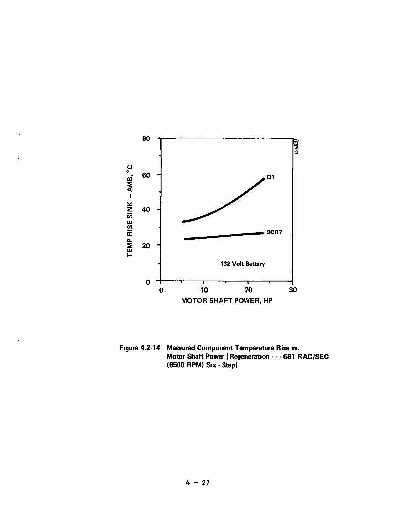
80 ~ ~
(,J 0
60 ai D1 ~ < I ~ z 40 en w en a: SCR7 a.. ~ 20 w ~
132 Volt Battery
0 0 10 20 30
MOTOR SHAFT POWER, HP
Figure 4.2·14 Measured Component Temperature Rise vs. Motor Shaft Power (Regeneration· •• 681 RAD/SEC (6500 RPM) SIX· Step)
4 - 27
SCR7
D1
SCR5
AIR FLOW
(2998)
Figure 4.2·15 Inverter / Charger Pac:kalle - - Bottom View
4 - 28
4.2.4 Motor Torque/Speed Curve
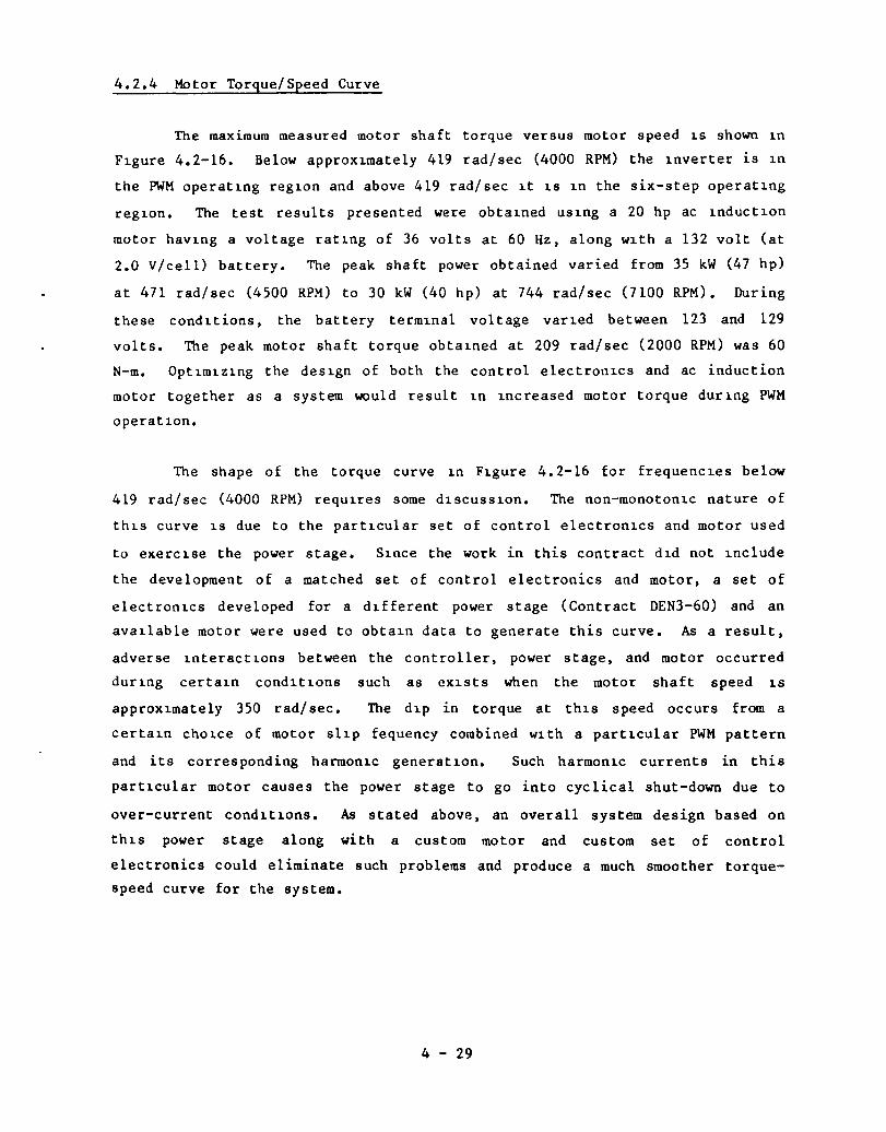
The maximum measured motor shaft torque versus motor speed 1S shown 1n
F1gure 4.2-16. Below approx1mately 419 rad/sec (4000 RPM) the 1nverter is 1n
the PWM operat1ng reg10n and above 419 rad/sec 1t 1S 1n the six-step operat1ng
reg10n. The test results presented were obta1ned uS1ng a 20 hp ac 1nduct10n
motor hav1ng a voltage rat1ng of 36 volts at 60 Hz, along w1th a 132 volt (at
2.0 V/cell) battery. The peak shaft power obtained varied from 35 kW (47 hp)
at 471 rad/sec (4500 RPM) to 30 kW (40 hp) at 744 rad/sec (7100 RPM). During
these cond1tions, the battery term1nal voltage var1ed between 123 and 129
volts. The peak motor shaft torque obta1ned at 209 rad/sec (2000 RPM) was 60
N-m. Opt1m1z1ng the des1gn of both the control electron1cs and ac induction
motor together as a system would result 1n 1ncreased motor torque dur1ng PWM
operat10n.
The shape of the torque curve 1n F1gure 4.2-16 for frequenc1es below
419 rad/sec (4000 RPM) requ1res some d1scuss10n. The non-monoton1C nature of
th1s curve 1S due to the part1cular set of control electron1cs and motor used
to exerC1se the power stage. S1nce the work in this contract d1d not 1nclude
the development of a matched set of control electronics and motor, a set of
electron1cs developed for a d1fferent power stage (Contract DEN3-60) and an
ava11able motor were used to obta1n data to generate this curve. As a result,
adverse 1nteract10ns between the controller, power stage, and motor occurred
dur1ng certa1n cond1t10ns such as eX1sts when the motor shaft speed 1S
approx1mately 350 rad/ sec. The d1p in torque at th1S speed occurs from a
certa1n ch01ce of motor sl1p fequency combined w1th a part1cular PWM pattern
and its corresponding harmon1c generat1on. Such harmon1c currents in this
part1cular motor causes the power stage to go into cyclical shut-down due to
over-current cond1t10ns. As stated above, an overall system design based on
th1s power stage along with a custom motor and custom set of control
electronics could eliminate such problems and produce a much smoother torque
speed curve for the system.
4 - 29
90
80
70
60 ~ I
Z 50 w :>
40 0 a:: 0 f- 30
20
10
0
0
PWM SIX STEP
132 Volt Battery Motor Ratong =
20HP@60Hz
2000 4000 6000 8000
MOTOR SHAFT SPEED, RPM
I I I i
209 419 628 838 MOTOR SHAFT SPEED, RAD/SEC
Figure 42-16 Motor Maximum Shaft Torque vs Motor Speed
4 - 30
5. RESULTS AND CONCLUSIONS
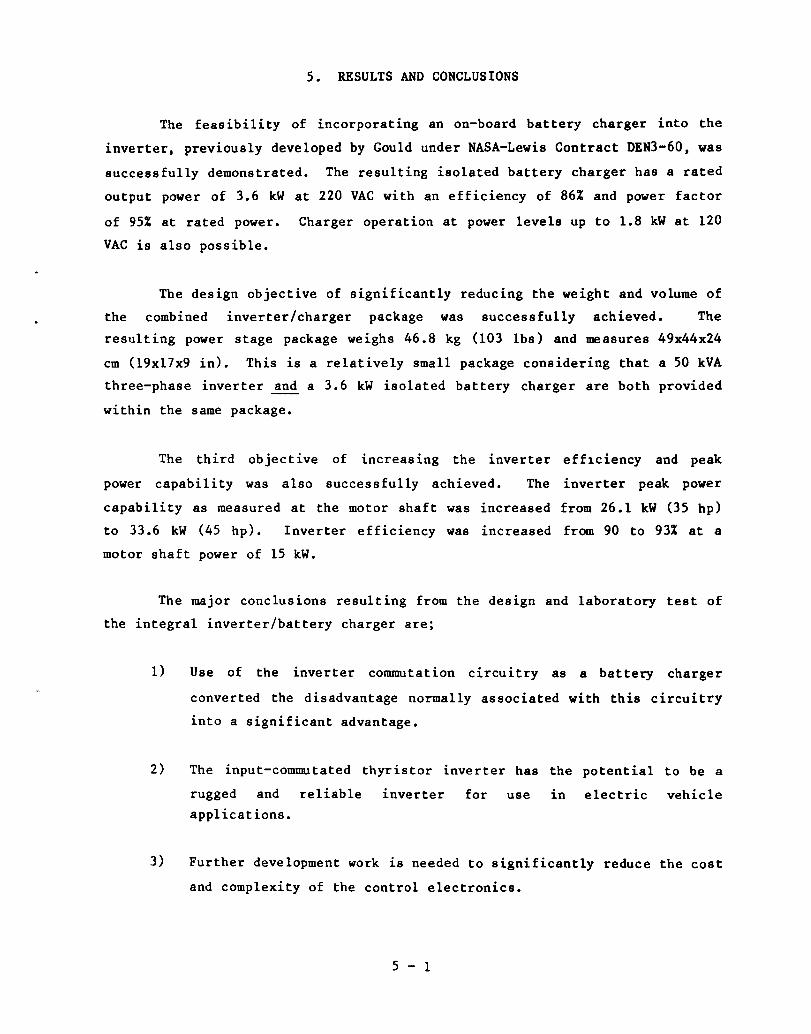
The feasibility of incorporating an on-board battery charger into the
inverter, previously developed by Gould under NASA-Lewis Contract DEN3-60, was
successfully demonstrated. The resulting isolated battery charger has a rated
output power of 3.6 kW at 220 VAC with an efficiency of 86% and power factor
of 95% at rated power. Charger operation at power levels up to 1.8 kW at 120
VAC is also possible.
The design objective of significantly reducing the weight and volume of
the combined inverter/charger package was successfully achieved. The
resulting power stage package weighs 46.8 kg (103 lbs) and measures 49x44x24
cm (19x17x9 in). This is a relatively small package considering that a 50 kVA
three-phase inverter and a 3.6 kW isolated battery charger are both provided
within the same package.
The third objective of increasing the inverter efhciency and peak
power capability was also successfully achieved. The inverter peak power
capability as measured at the motor shaft was increased from 26.1 kW (35 hp)
to 33.6 kW (45 hp). Inverter efficiency was increased from 90 to 93% at a
motor shaft power of 15 kW.
The major conclusions resulting from the design and laboratory test of
the integral inverter/battery charger are;
1) Use of the inverter commutation circuitry as a battery charger
converted the disadvantage normally associated with this circuitry
into a significant advantage.
2) The input-commutated thyristor inverter has the potential to be a
rugged and reliable inverter for use in electric vehicle applications.
3) Further development work is needed to significantly reduce the cost
and complexity of the control electronics.
5 - 1

4) Development of an ac induction motor specifically for use with the
input-commutated inverter is needed.
5) Development of a PWM switching strategy designed specifically for
the input-commutated inverter is recommended (DEN3-60 recommenda
tion)l.
5 - 2

6. APPENDICES
AppendlX A Charge Control Board Description
AppendlX B Set-up Instructlons for Inverter/Charger
AppendlX C Schematics and Drawlngs
6 - 1
Several protection and lnterlock features are incorporated into the
charger control electronics. These protection features are;
Note:
1) The motorlng functlon lS disabled while the charge cable is
connected.
2) Should the battery voltage, durlng charger operation, exceeds 2.75
volts/cell the charger wlll shutdown. For example, if the propul
Slon battery lS accidently disconnected durlng charger operation.
3) A 20 amp clrcuit breaker lS included ln a separate ac line interface
unit. ThlS unit would be located at a permanent charging facility.
4) Power lS not avallable on the battery charge cable, which connects
to the power stage, untll the charge cable lS connected to the power
stage and the keyswitch lS turned to the charge position. This
safety feature lS provlded by the ac llne interface unit.
Use of the ac llne interface unit lS not required for charger
operatlon however, lt is recommended that it be used for safety
reasons.
5) Should the charger not transfer to the finlsh current reglon after a
pre-determlned period of time (Tl in Figure A-l) the charger will
shutdown and the charger fault indlcator on the control enclosure
wlll light. This is an indication of a possible defective battery.
A - 3
Appendix B
Set-up Instructions for Inverter/Charger
Presented in this section is the information required to initially
apply power to the inverter and battery charger. The major system components
are;
1) Inverter/Charger Power Stage (Unit 1)
2) Control Electronics (Unit 2)
3) Accelerator/Brake Assembly (Unit 3)
4) AC Induction Motor/Tachometer (Unit 4A/4B)
5) AC Line Interface (Unit 5)
The additional components supplied with this system are
6) Battery Connector (P5)
7) AC Line Cable to Interface Unit Connector (P3)
8) Motor Cables (Ml, M2, M3)
Prior to applying power examine the system control drawing (SK-142082)
to establish the location of each major component (Units 1-5) and how they are
interconnected.
Motor/Power Stage Connection
1) Remove the power stage top cover and locate the three (3) motor
bus-bar connections labeled Ml, M2 and M3.
2) Connect the motor cables labeled Ml, M2 and M3 to the power stage
bus-bars having the same labels. These cables must be routed
through the cable clamps and these clamps tightened.
3) Connect the motor cables to the motor leads labeled Ml, M2 and M3.
4) Replace the power stage top cover.
B-1
Inverter/Charger Power Check
5) Connect a l50V, 10 amp variable voltage supply to the battery
connector provided. This is a polarized connector and is marked
(+) for the positive supply lead and (-) for the negative supply
lead.
6) With the supply off connect the supply to the power stage.
7) Slowly increase the supply voltage from 0 to 150 volts. Move the
circuit breaker handle towards the motor cable clamps. The supply
current
towards
should be less than 0.2 amps.
the charge connector on the
current should be less than 0.2 amps.
8) Turn-off the supply.
Control Electronics Power Check
Move the breaker handle
power stage. The supply
9) Connect the tachometer polarized connector to the control
electronics.
10) Connect the accelerator/brake polarized connector to the control
electronics.
11) Place the accel/brake direction selector in the off position
(neutral) and rotate the accel and brake control knobs in a
counterclockwise direction until they stop.
12) Manually move the circuit breaker to the charge position - breaker
handle pointing towards charge connector on power stage.
13) Turn the keyswitch located on the control electronics front panel
to the off position.
B-2
14) Connect the control electronics to the power stage via the
polar1zed connector on the control cable.
15) Increase the power supply voltage to 120 volts.
16) Turn the key switch to the charge pos1t10n. The fans located on
the power stage should operate and the current drawn from the
supply should be approx1mately 0.6 amps. The overcurrent indicator
light located on the control electronics front panel will light
momentar1ly. The remaining indicator lights will not light.
17) Turn the key sW1tch to the off position.
18) Move the circuit breaker to the motor position - breaker handle
towards motor cable clamps on power stage.
19) Turn the key sW1tch to the motor position. The inverter power
stage wlll "beep" and the motoring indicator lights on the control
front panel wlll light momentarily. The fans will also operate.
The supply current should be approximately 0.6 amps.
20) Turn the key switch to the off pOS1t10n.
21) Turn the power supply off and remove the battery connector.
Battery Connection
22) Connect a nominal 132 volt propuls10n battery to the battery
connector observing the polarity marked on the connector.
23) Connect a separate contactor in series with the propulsion battery
to act as an emergency disconnect. This contactor also allows the
power stage input filter capacitor bank to be precharged before
battery voltage 1S applied to the inverter
B-3
Input f1lter capac1tor precharge
The input f1lter capacitor bank, located 1n the ac inverter power
stage, must be pre-charged to 120 volts prior to connecting the propuls10n
battery to the power stage. If this is not done the capacitor 1n-rush current
when full battery voltage 1S apphed will open the 200 amp input fuse (Fl)
located 1n the power stage (reference the system d1agram, SR-142082). Dur1ng
actual vehicle operat10n pre-charging the input capacitor bank could be
performed uS1ng e1ther the ma1n propUlsion battery or a 12 volt accessory
battery. S1nce ne1ther battery source 1S supplied with this system a separate
1nput capac1tor charg1ng C1rcu1t 1S requ1red.
The pre-charge C1rcu1t used dur1ng our testing 1S shown in Figure B-1
and allows the 1nput f1lter capac1tor bank to be charged to 120 volts prior to
connect1ng the propuls1on battery. Use of this circuit 1S described below;
24) Connect the pre-charge C1rcu1t out?ut leads permanently to the
battery power leads. Th1s connection can be made either at the
battery connector or the battery contactor.
25) Adjust the 1solat10n transformer secondary voltage for 90 volts
RMS.
26) W1th the battery contactor open connect the propulsion battery to
the power stage.
27) Charge the 1nput hlter capac1tor to 120 volts by clos1ng the
normally open push-button switch. Measure the voltage at the
output of the pre-charge C1rcu1t and as soon as the 1nput capacitor
is charged to 120 VDC close the battery contactor. The pre-charge
C1rcu1t 1S rated for transient operat10n only.
B - 4
2 AMP FUSE SLOW·BLOW
AC LINE 120VAC
Figure 8-1
VARIAC GENERAL RADIO W5MT3
100n 5W
ISOLATION TRANSFORMER TRIADN66A 115V e 217A
MOMENTARY PUSH·BUTTON SWITCH (115V,1AI
...&.. >--........ --....--. +
DIODE BRIDGE 4-MOTOROLA 1N4006
43000 lOW 120V
PROPULSION BATTERY
(2625)
AC Controller Input Filter Capacitor, Pre-Charge Circuit
B - 5
Charger Operation
28) Wire the ac line cable to the interface unit connector for 120 or
220 Vac operation as shown in the system diagram (SK-143082).
29) Pre-charge the input filter capacitor and connect the propuls ion
battery to the power stage.
30) Connect the interface unit charge cable to the power stage via the
polarized connector permanently attached to the interface unit.
31) Connect ac line voltage to the 1nterface unit via the cable wired
in step 28.
32) Turn the key switch to the charge position. The circuit breaker
will automatically move to the charge position, assuming it is
in1tially in the motor position, and after a 10 second time delay
the charger wlll operate. The initial charge current will be 10
amps at 120 Vac and 20 amps at 220 Vac.
Motoring Operation
33) Turn the keyswitch to the off position.
34) Disconnect the charge cable from the power stage.
35) Manually move the circuit breaker to the motor position - handle
pointing towards the motor cable clamps.
36) Pre-charge the input filter capacitor and connect the propuls ion
battery to the power stage.
37) Turn the keysw1tch to the motor position. After the keyswitch is
moved to the motor position the inverter will "beep" and the
motoring status lights on the control electronics enclosure will
light momentarily.
B - 6
38) Move the d1rect10n selector to forward (FWD) or reverse (REV) and
rotate the acceleration control knob to activate the inverter and
motor.
39) To stop, turn the accelerator knob to its minimum (MIN) position
and turn the regeneration knob to its maximum (MAX) posit10n.
40) Turn the key switch to off.
41) Disconnect the propulsion battery.
B - 7
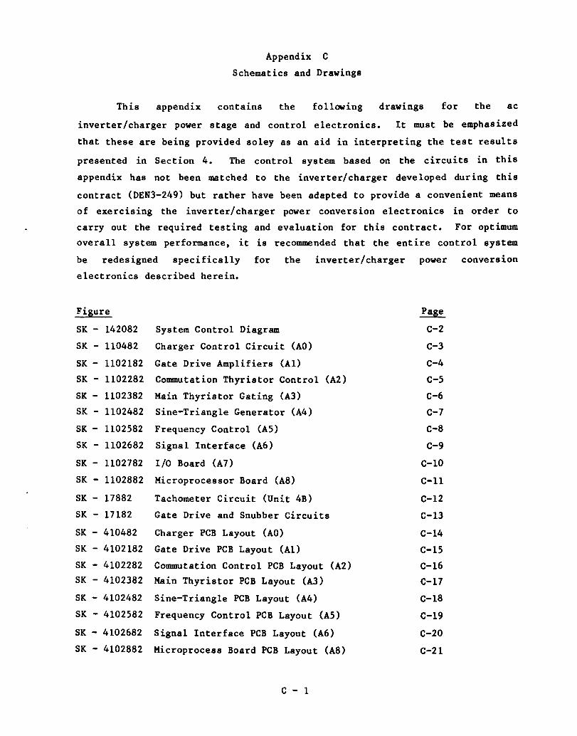
Appendix C
Schematics and Drawings
This appendix contains the following drawings for the ac
inverter/charger power stage and control electronics. It must be emphasized
that these are being provided soley as an aid in interpreting the test results
presented in Section 4. The control system based on the circuits in this
appendix has not been matched to the inverter/charger developed during this
contract (DEN3-249) but rather have been adapted to provide a convenient means
of exercising the inverter/charger power conversion electronics in order to
carry out the required testing and evaluation for this contract. For optimum
overall system performance, it is recommended that the entire control system
be redesigned specifically for the inverter/charger power conversion
electronics described herein.
Figure
SK - 142082
SK - 110482
SK - 1102182
SK - 1102282
SK - 1102382
SK - 1102482
SK - 1102582
SK - 1102682
SK - 1102782
SK - 1102882
SK - 17882
SK - 17182
SK - 410482
SK - 4102182
SK - 4102282
SK - 4102382
SK - 4102482
SK - 4102582
SK - 4102682
SK - 4102882
System Control Diagram
Charger Control Circuit (AO)
Gate Drive Amplifiers (Al)
Commutation Thyristor Control (A2)
Main Thyristor Gating (A3)
Sine-Triangle Generator (A4)
Frequency Control (AS)
Signal Interface (A6)
I/O Board (An
Microprocessor Board (A8)
Tachometer Circuit (Unit 4B)
Gate Drive and Snubber Circuits
Charger PCB Layout (AO)
Gate Drive PCB Layout (Al)
Commutation Control PCB Layout (A2)
Main Thyristor PCB Layout (A3)
Sine-Triangle PCB Layout (A4)
Frequency Control PCB Layout (AS)
Signal Interface PCB Layout (A6)
Microprocess Board PCB Layout (A8)
C - 1
Page
C-2
C-3
C-4
C-5
C-6
C-7
C-8
C-9
C-10
C-11
C-12
C-13
C-14
C-15
C-16
C-17
C-18
C-19
C-20
C-2l
r'"'" ~ -r~ _-=-,.~. ~·::iB=:B~.;.::l · II L ,r,'!S_~ "" __ ~_' - -_~~J f~H ~----------------------------~~-----------r~~-------+~
CelA A9 05
,---1.-,« : ~ I 4 '" r . =';"'~--------""""''''-''r---------;-+--+1+-r--------rl-;;:;-ItT'" .... ,..,,, 13r
J? JI~ lW<
II II CA I ,Dr,
M2
.'13
"11
-~.:--;-:::::--- ~=- -- ,--__ -:r::::-"",. ~_\-- --- "'-
I
1 I
~ W4 CD"LE
rJN1iif..A
...----------..
-8?-~ 7E~r"",
_/
t- t ~- - n I p;?jCAl''-E I ACl~%'t0irlkFAc~-r
1/18. ~8?".,_ I ;:4/1.I~-+---------. L+--<~ I I I J II I, I lc~ _~~N B Y,w ,- ~S>4-~ +---+-----,
'" j I ('I I~ ~;:1 :~ 1~ • rTl~ all , .. [.
?2r IC2Cf.
J/
~. ~ ~I
. . , . , ~ , "
~~;l /CIo, A3 "'.. ~ 0':"'1" n . -. D2 {.! '~':'" .~ I ~-+'-"'-1 '''' ?+-f'1 ,.
U~~ITIm · I ~l~ 6
- - -~-- - -- t ~+U- - t-~ ~ ~ ~ -J3
----+-+---++----++-+-+----+----+-+: ;!l ~11 ~I ~; l
~ 11r.... :::: ~ ~,... f\" ! = ~ In ~ ()
.5"''''''''''''",
" • ~ '( ",- : ~;:, ~..:; , .:: .:;.... "> ~ .. ~. C'~rtlr;~ R,,-- ;; ~ ~ ... ;.-
______ ~.M""NrL- _______________ --_-__ ~ 1 __ - ---, ::~NM ~ I :;;S#EMAT' j;)/A&I-.qM en5 I
.- A - C""" I
Co,.,
;: 1<: ~ I(
~
" J .. " < , "
~
<
j" • 11 . ,
NlS:;IlB~E
WCD~
- I .-/~ I
;;>Ir\ C-",- ",,.~~~~ ~<f<fq:,,,~ ~~ __
't,('4~~;~q ~~~~~, ~q~~::~ . , • I; 'l '"l'lo..
~ ~ l' . . 11-11-111-1 +--"' JZ -1-1-1-1-1-1-_-_J"2 ___ ---4-i1-++++++++-+--_
PI 1 i.[!'t1-1'r i ~- PI P;?- 1t-.f2f-lf-Lf-Lff- - P2
-, +IT1tt~ ~ ;
SCfi>//::~ c/l-I'f:"c/r':- -:: A
~OR~ ~N/"I -: B
~:cr) ~
JtJ/~2 FA'IJ,. r PA~/Ff-
PI
l- w2 C'AlJL~
UA/,r 3 I I I r -,."'''' -- -
~... I I ' !k~ ~.;. rrl.;; . lli=: ..
W.3 CItIlL~
vOJ{r41!fJ
=';'1" 1 I, n I 1 ~/. 6 /0 Ell 6'1 EIJ
I ~CH~lI$frIC ~y'A_"'1.. .:s:r_I?~---'2 =~ _______ _
I i I ~-
I :: L-I __
~'~_=J~ 'i I -~ ~ ~~::1" -2;??.J
.~ R4 ~_ ~~,.~ ~_c:- ,."
vvv----L.-¥'~-.:; r;;OJ< C.·~I ~,.".
-~ _~IO/l-
(),,';UIt""~ ~t:: .F __
--i 6"''' .:£
'!l_ •• :;.,::~ _
~o •
_J
/10 vAC I , .~T6':C £ ==r·') L~_~;'., D
TRLA/C~ ~/. --<E'
IJ] I .. t)- ( ... " ~ ~,., 2'~O IIO..-AlC ...... c
:'AlC ItVAC+W'~'
I ~ ~ " lJ -~ ~oCI
~II 0 ___ I~~!E",( L-
.~
-Ff -0-~
~" r---
-, u) --
~I'N -B! L-
l-_:~:t - t 1"- - .1.- -t - _ 4
~=J L 2-'
P/I,RTS LIS r. PL -51;' 14E082 ~ ~"-1 I -~=-: -=--! _NA~ _ -> GOULD _._--::=:":.
SK - 142082 System Control Diagram c - 2
Ti'" .... 5 It'
Vi I 1~ll 0J'1 ~ - 11 ... \1
< I l "'0_ 1 C5 t" OOjA+ !;3, .. 1 ..- Jrt ',- ;< 'II. Y I
,",,0 > t .L J. ",.'" · · ----1:~ ~z ~. ~~~ V
T ........ I~f --.- 1,..1 ,()o~f _
"" II &0l0i0 -15'1 .~0.1~
~~g- ~ - .. -llV
>:1 v, (ii>--~ ', .• .-
C8 J li"
I --it 75~', /1.: ~IB ~ _ -/'v '5' • 200 • RZo '!. 1 lIt' Ill'
1"1. ,L 'L· 'I J.('AI 1"/20'11 t I' \. -.? U7 ~
c..7 ",1M
- 3 +' RI<.J <...
t.O.1( I~
~<'
", ~~. 1.0
1 R2:, f-~IG'~,.I n, .z~~ h ~ 7$ ... '''4 ~ .... ) ,JijI1.
11. ~91'"
RI 5K. v ...
C V'v // Z 7V/ At- ....-- /UiI..L
010 -.)/( (" +IL L ut I,..
c-"-. T3-+-~~
+/~
I , /(11
<' /0 ~
U3 '
__ ,f12 ..zJ ,>1239 V -'\ / L+ ~. ~If"
t
.. ~
lOA ,&2. RI3
f? 2 5 l -------" r. /J r.-- "" ! I.
Q .,:+-t- v... I
101", I ) 3~'-_ H'/<m <~: I U3 "
/?Ii> 51 L"Z3~ ,2 - ? ,/ "'V\/\rf1 + • -. -- YI!
10< IV?
I"
~JI
'0<
.qZ9 zooX
~Y"">,.-, +<Zt;1 ; -o,~:
_1 ~)f'; 1)9 ~
t-f!FlSS"I '"
'HHI '11 ~ ~ r
C'S ,oo~ 1f54
t /).. -
1 .. T, ~" u4- • .i..
'/ +OIJ -
1-'12,. .s1P
.. 4' -' . J(p 4-
- . I
+<~
r \'" I •
, III' IJ4 , .>
.,'
<31 -- +IZ 1,.1 TRJ7~,1 7 5~ 'I
" I
3,
-i. VIJ ..
5
00$'7
1ICO
,. :'=t-jl' ., "
v_. 10'1 !
G30 !Jo.+
l C33 SOOI81"'~
'J.
01 ....
-"CD
i'lUNt+ [V
o z .. " --.. ,'I, J It~u .",~H=j I' SoIr 'l70,' +IZ
• ",\ v,,. ~ __ 1<-.0 I "'17 •• ': :r.~1 "44 " ViZ ~ Z ""'" ",,' , ". ," ~" , .. , ~- ., , + ." ...
' '- v '0 '-; ~ I ~ 0' I 10IC 81 f .., ,.,," , L"1" ~"-"'M" 41/1' ~.' -, •• .., ... _~ _M' ._, . ~ , ., . -;;; + •• .. , ~, '"'l , I. ,7 •
~
<. V IIU --"\.'VI,--
ZZO"l C.C $IT
~ ""'... '"'' . '- - ,·r .. , _ • .. ~. .., - I •. ~ .. f. HSJ
i 'A-.~
C~u;,:T ,. ~~- A .. .,.',~ l'.r 40:: " .'- ( ."' ,"
::r'L. Q
SK - 110482 Charger Control Circuit (AO)
+ 102
R."i 10K ~
+IZVO
I
J
+'2 I,. f.l U30 t'- 1\
HIIAI; ~I!:,~I
[" ,.'148 R" 10K ~
'O"
/J'~ ,,~ '3. '':' i -- 001 __
) ~,' JM • ..,.
,'20 V J i'IO'V
lool<, 111.0.
"'" A''''
~ ~ .. 1211
R?4-'0<'
cDI;<f
AEYlstONS --~---~ -
III """""" ~.
S&L&~
" ,;t: I~f
)'-p
ill
ZJCiiG •• CAtER
"lCAO ...... TC. ..
-----1----- I~ II
liZ
At LINE CONNE'TED
;[) 12
14- 31 c:;:-o:..:---t"
RilE> ,0<
.Il
~I 1024114
~ I(
-~~q VV'v /,"'-
.,l R ~ 7 ---<:ll ".s
TOI..IMIICU I*L1U Ot ....... IPK .....
.-...c:ftOII ••
/IOULD INC ..... NOI"Nn"", ..... ,. ... , ........ rt:1MAI.
DO NOT SCALE THIS DRAWIH,
'o~
-CtiKilio
~
-) OOULD
c - 3
Ac
ffJ)~ J -
L-JIO .1.
J..'AJ,c;z.""" /0
IUWIDU) AC. LI'l" v~TAM
~,~. I
,lVAJIfI CNA~,.,rL.
Ce..A""'#ft.. c,t/(",-r~""'-~"''''''T/(: .. C'~i"I\:,,..,, DU. __ •
SK-/IU482.
1"0
'--'1"' '~L j!': -~
5. .se,rz.. .-l.u J:u
,,_-=-~~ __ II
sc..~4
~ ..... I.
1'" lU
'S--~Gl"!>--~ -, .,. 143
fJ.. , " §iW4 I~ ~I
CI
r
~ J.1:r~
... ,.. .-.J,.A
~~3L-__________ ~ Li~)
t;:.-n 1/
~ fr..z. IU7 K/4 -6 ~~4~ __________ ~ ~I·~·J
, 6
-, .•• ~.<.... '.t .,. ...... n
'0. .. .., ,% ~........ ~,..,"'''--..... _____ :...... ___________ ....J ... , ...,..,
::C .~-0~ 9
CUf"\ ... "Ik..5~L~ ~/O .5 ~., I 8~ ~4
, ... s •• +Il.'i
r--MJ"8100
C" CR • .flo! z.ol
It IS CIir,Q c., 7~t...
Ill. 75c.
1f!5' 56.n.J 5l1li
lo-~--IIf---l-..".., -lSI/
--"
./1II;::1:..:8:.:I,;:OO~ ______ +--<lI.
CII~ elf" ./==-"",....0':":'---1
CII. ell7
c.R2.,
""'
p ... 7St.
2/3 7.SI!-
I!I~ Z5lt.
A!SS Sbst" S"':
.. ~ ....... --~I---<~- -15>1
!4r.'oo ~
..
,....- ----
'. ~--~ Itl
M"'BIOC 15
fiff.,sw ~""'----n---""<Q-'5V'
1'1.18100
s1~,sw. O-~---IIt--""'-o-15V'
MJ'8100
~J
,n
~~~~~--~~r-~~r,r-----~O·
--. ____ --:;cO""E"'V';;;S.ONS ._d .. I
1 oury",-rr l\tljAC c.H r ~ or ... , ... 01\4""
~~ Off 0" ...... £1"1
ALL OOODE~ - iN4148 UOII..E •• Nor£O
ALL An.I.T'OIt.$- "4'" ,5% t.WLe_ oIIOTeP
NoTE rH/~e"ARD I'1"'D~ F"''''''' /!r-"",,,,, FI"'~r t.lsFtJ t!JA/ .5r:,.,4·...,~-r/C ..... -,//080 ~V'
..--..mpi-
· -.. ;~ f~~"~ '-------- .. ~ «sQ ' I ~ c.a_."... ,;.,..,
I~ = CL .... " t.""", ,..
·I.J,.A ~" ~6. U7 ,
-~:'":6 : 401', "
u5
7 ~ r--------------------------------------------=:=:=:~----------Jl-----------'g;~'-. v
1 TIS'"
/Z44 t5I
?"~'IL. z.t)LrU..~~ ~lS!I Cl,O ,q~-?! IlL
_ .4'1J<f TIg;
":1'8.00 011 -' 64'S C3B ~·-.3~f
~I i~:,5W ~lo-<I -ISV' ~
ct; ff. 4071
4O.V. +~v
SK ·1102182 Gate Drive Amplifiers (A1)
r--.... ---.... ---~.-.!..l'1 ~.&.I~ n+l7.V
CJD. 4)J
c~.
'poi LA&T c.J~~D""~
UII C.4 Reo 02.S Q2.0
25 PI~ CONtJec.TOIC..
TGUMIIC." """Iii OTM ...... SHe ..... - .. ..... eou&..1IIC MA' HIOP'III,f&JIIT JlllQMTI' ... ,' .... 'IJII'A~
DO NOT SCALE THIS DRAWING
--CiiiCUi
-> GOULO
c - 4
PARTS \...15'1' .... .... -..I.A8OAA,.,...
JIIOLLJNOIllADOWIIU_
PL-5\(-!" __ ~:.
.. ... GATE DRIVE AMPLIFIERS ECj-lc'~,.rlc. C/~-:;'k~""'" 1-11 .... -----.!.- -
;:'J(-//oaf3:...
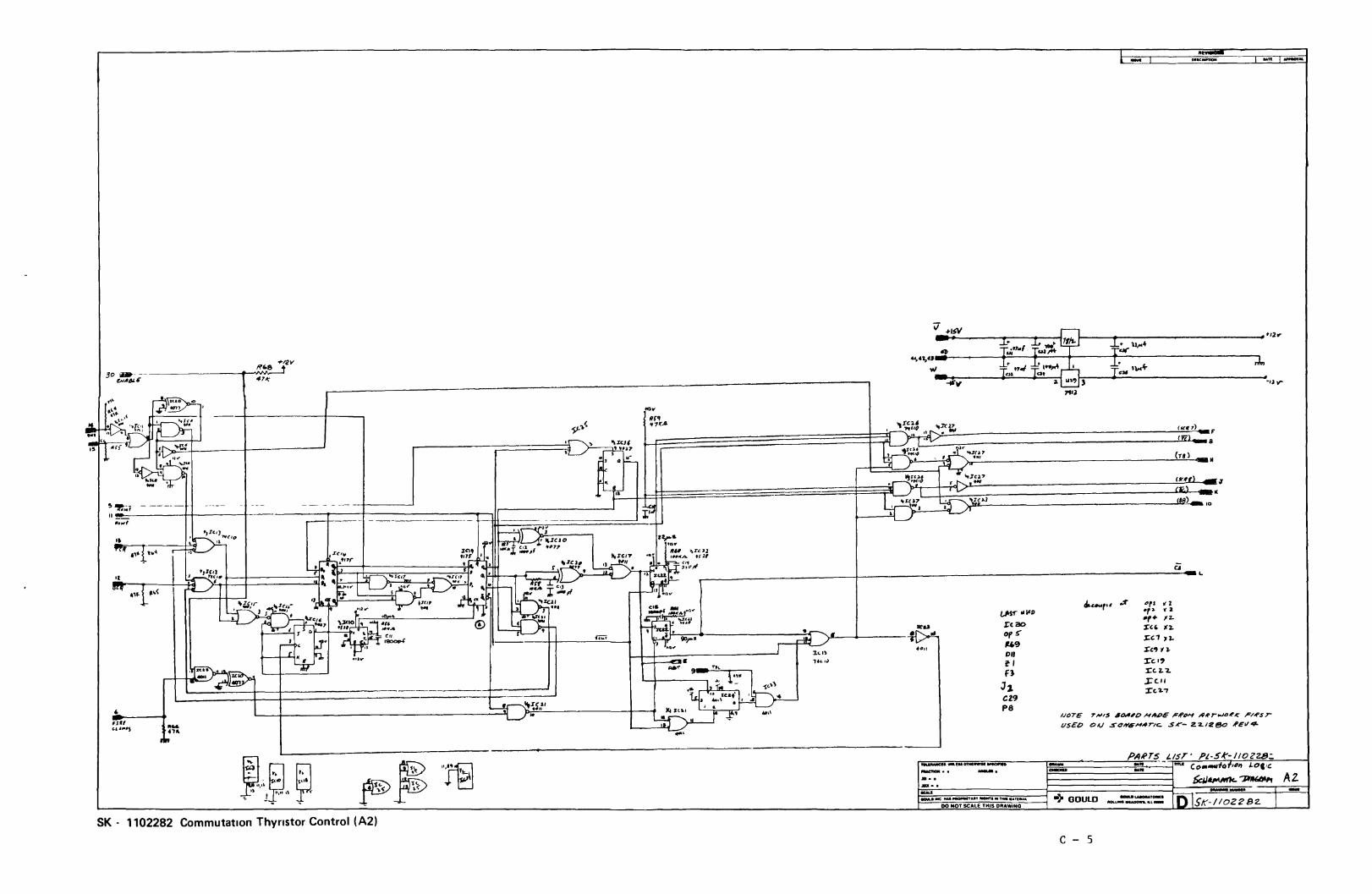
30 11»~A4J..
+12 v ~ 4710;
~ ~I~
.M~ DIln. I",..",'"
r-----~1:;-~:;~-----------------------~t'2~
''''~ ~ ~r
'IC'p) F
'-~8 ~~~=:~~----------------------------------~(~T')
~L-__________________ ~~~:::J Iol
~, :';M' II 1___ _ ___ _ •• ",..t .....--1-----. -
I. 'J IC/
) 7W C'D I:~,;' ~~ ~.~
It
IIPt ., .. i ,.<
, flit
""""S "" n .. I..
~ ... ~~. .. _ rio", s",1
11,.l f"
~., 1 .... '" 1\ "
~ PlW
SK - 1102282 Commutation ThYrIStor Control (A2)
"ffi
c/,.UWr".:r "'rJ ~ 2 .r' Y Z /.M'f" "I'll .". 12-reDO r(, 12.-
CA _L
o,,!: ~'1 ,2.-
r.;;; u,g rC., 'Ilo ---4+-----'=---1 •• " DII ]:"c.
I
,
,.. " l" / rC. z. '2.
f) J:C.II
J 2. :rc."I."7 CZ9 P8 ~;S,f' ..
~~U.OTMI""....aI'IIO - .. --. .... ...... .... _ .... ~AII' .... T .... ,.... .... tllIIAL
DO NOT SCALE TH_IS DRAWING
I/OTt: r"'''$ 4~'O H,.Pt: ~IP",'" A~ro.JD'A: ~/<f'S r (/SeO OA.) SCIJIGH4'-/C. $,("- 22./280 ,fEll ..
-iiiiCiii
PARTS liST' Pt-S,f'-JI02Z8:;, ::: -- I ..... Co .. _ tO/-''''" LOC"
ScU~~'" AZ
-> GOULO --.-.,_. '0' --__ ...-..L'_ IU LSK-/IOZ282.
C - 5
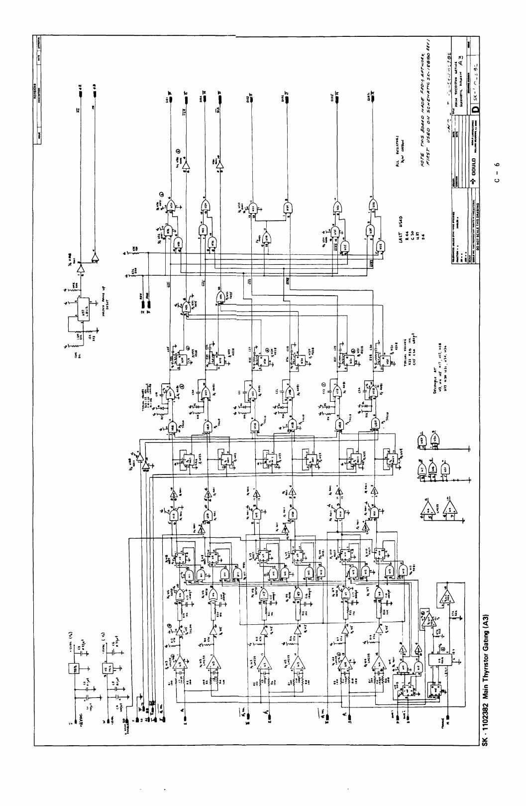
..... ,. ... '"
~2 <> q)
~ " I... " ~ ~
.. "It) .. ~ II .. .. , t-IL '" tz III ~ I ... EIr ../It I( It
~ ::: ~ . It. ~ lit ! .:& .:& .:$
I: ! Il ~ :t
~ ~ ~ Q ~ ~ ()
~Q ;; VI ~ ~ .. ~ '" .. .z I.:
(3) ;; ~ " :t ~~ ~I" -' l
U ~x ~\ !3 ~ c ::::I 1.0 ... • 0
Q
U
Q • •
Q
l :s ., t; :~Ii" ~
..... :10
U 4
... :;: -t
I~ Il Ii ~ ., , II
it s I ; ;~ .". . ., ... . . L-t;W
1:< .... !
~ .. " 0 .., ; ! , • : IQ.
" .. s ~
~: .... -,
~:: ::: -. :;
~ .. - 0:: -. .... '" -
'-:s .;; c .. ' ... :l ,; ~ 6 _~ i; ;
c; « -~
+=i ca ~ ... 0 ... III ~ > .c l-e 'Ii ~
N
.. .. \! < ! " ~ 1 N .. ., .. J c 0 po po
~ (I)
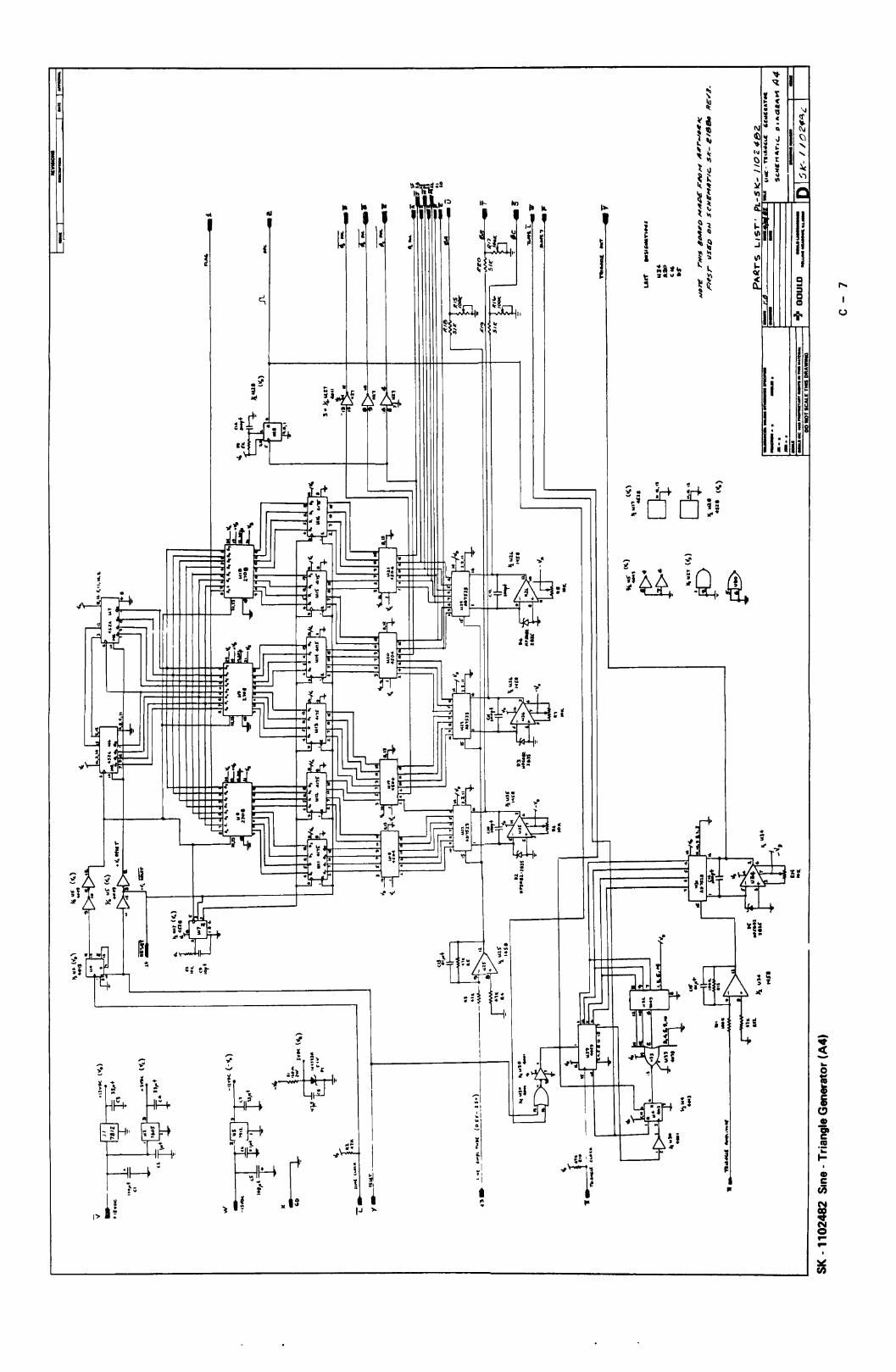
... II M i I I
~ ~ l!
... _. , ..
.. i...J j; .. ... ~'.~'{ I g
:. ~F- i !fi8 + .rio
ar -; i" I~ ". .,
"
,.. -t ~
~ ~ ~ +
~ . :-r1~. HA .. '" ,- ..
;~ ~ ~ ~
. :--I! :"
I"> i;
t~ I
., • ! ~ 1 11'1
* I.J ,.
~~;! Ih
Ie ~ .. I-;)
~M ••
,I : " i • ~ 9!
Q I.e .. , " ..,
-
.... = t :
... H~ 3. ~- ><;"
I~
I
I i
It". !,i . .. ~ . _. ~'"
'--........--...... I-I ! •
..
~
'!!II .J
til ~ Qt
! I':
II "-"-'+..-.-1
h I f C
Ii !i I ~ I. Jig
II'
0' W
~ iii '--
~ -
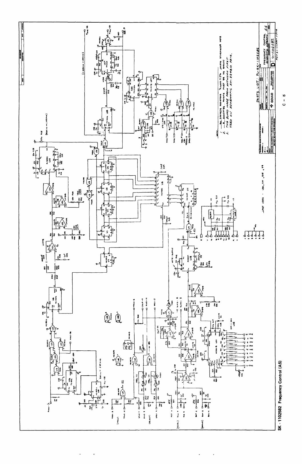
l .. ; -t ~
~ 1 •
I :
r .. 3
't- \ I:; -
;~ •. II! II ~ .. .
. 1
!, I
~ .. ~ 0
~ ~ t ~ ;,
.... r ~ .. _0
:: G E .-•
, ;" !~ \~l ~tr ~ ;
2 " Q
~ 1 . .. :l :l I
~ , • 1
i , .." -:;
~ !"
~ • • , ,.. • · 1
l1li I; :it
" j " II ~
l; ~
I.. " .. "2 III ~
I i I ~ 0 ~ ~ Cl
• It .. r \ 1\1 In III Q III " " "l 1= ", "I': " \c J" , "I < " _ E. ~ \J
e ~ : iI(' ~ l Iij ~ i ,~~
.. t ~ If .. ~ ~ ~ " !I " ~ ~ D '\ _ a ~ Q
1i~~ '""-vi
.. ;;
r ::
i .. -.. , " ~
• u e,,~
-..--r-~=---. a 1~'
.o ..
in « -o ... .. c: o
(.)
> g CD ::l
~ u..
f8 N o po po
Xl
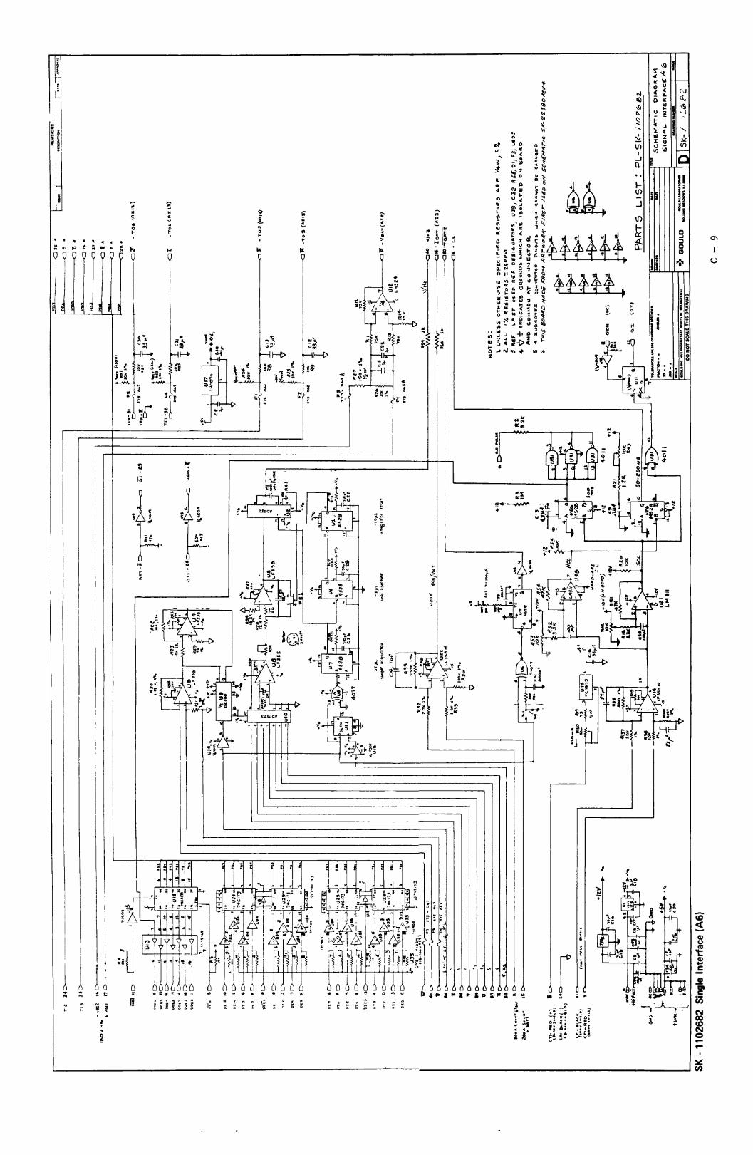
,
i~ II I
,.. -: ~ ~ ~ ~
IJ .. " It .. .. . .
~ ~ i .. ? .. Q
t- o , ~ . ~lcJl'l~~"a.~
I( [ to. ~ 10
I I I 1
I
:l ~ , Q
I;; .. Cl
.. l· 3 J S ; f
- '" ,...
-. ~ ~I o· ~.
h
. ~ .. !O ; Cl
:::_ ~~i.!-~,; ... '---T "'... f: ... rt; c.:vo -
. I;
! .. ~ .. • ~
IE
0;-w
~ ~ • '> ,
IlL
• .. ... ~
~C?t r- .; • !.-O!~
I
'" .. , ;:: ~
v
I
1
.. ~ 0: ..
: ~ ~
=
"'~ "'-to
:+
- --~' ~I
; f . . '\.
~ ;I~;; ,J'
!! . • ~f ~ J ~ }t
~}~ : ~~c! +t1'1
• , J!~ ~! ~
r ~ J; ~ iif. ~ r~~ aM ~ ..: ;; ~ I.. ,,........ -... en -+ ,-J~ N
I
~ f 00 .. t CD
~-------------------------~;
u
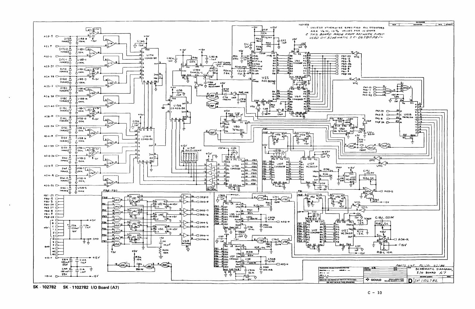
Al",- 5
1\ I I ,.
AIZ-U
"'13-31
AI4 36 0 IOI.~
AIS-V
AI" ~
A17-4-0 Do10lr::t t"a"-~I .• ~ I 3l
A16-1:'1
.0.1!j- 34
-'IIO-~
"'I"-~~
"1/3->1
"114-11. 0 ,j
A115-35
pe1 -25 pef>- ~ pes- -e PII4-Z6 PII3 27
pe2- t: PI!> I' J Pelll-28 e>--'
6 ' .. +5V
{
A D
1-5" c 1
2 3
"" .. { : 41
4l
4' .,S-T
-15-~
GOlD
----:t--t----.. + 15 II D C8A it :t CIOA
I';S-VfT T Il..lf
c._ J: 1w.. ::!-looAMI I I"". -
D '25'1 .. -15V'
SK -102782 SK - 1102782 I/O Board (A7)
+sv
R9" 101/1:
ovr~
01".&
+ IS" -ISV
-I5V
OJ I)A..~
NO"~S \ UNL-ES~ OT~ER.~'~E ~p~cIFIED AI...l.. ~E'S'SrDIt",
A~E '/4"-',10'7 .. VA'-UE5 ~ ... e: 'N OOi"'!l
t"!'>'"
t? TrlI5 B~""RI? #/90£ FIf'~M /9,erwplf'l< PM"Sr
VSEC? ON SC;ycH,.,;r/c S K- 26SBOA'G./-ell I .... ~
241131 .A I~ Co~P -r-lii v" '.As ,., .:2- " , .. ,,,) e. " ell AS... .--. P&7 25 unC
Be B7 "'7,~, ,.e~- ~ ,,3 e" U .... J AI. PBs-I!) .... 3 4I!> SCD40"IeEA5 ~~ ;::; P&4-2'" "5'~ ~ A4-III~ PII3-2? B~ 1 " &3 "3 1 PI!>2-. 87 r.-; '&2 A2'7 PIII_ It 8s 1 el 'II '~ ;::; pe,-26
U?1. ADe:SOA&-
12
8, 1'0 "1
/1
Ulle:
P"'7-21~ P .. ,,- y -. "
P"5- ? P"'4-2'2~
f'A323
PA2-.I.
PA~-&
PArd 24
VII
A04-R.
.! lsI/
-=-
REVISIOHS .",MWA&.
I.~ ... 000.... , 0 "01-0.1 p.-.pr (.'5r p,- -:-,('- ? :fe' 1OLIMMCU. ......... 0',.. ..... ...c., ... - .. ..... eouLD.c: MAS~n •• 'ffllOM1."""'."'fI"","
DO NOT SCALE THIS DRAWINO
--....... -> GOULD
c - 10
.. .. ..,.,.,e L.AeOI'AI'CMMU
MM.u...~"L __
5C. "'to MAT"IC. D IA"~'Vt."'I) r /0 ~O"'RD ,4 '7
... --- -K- 1/02.. 782..
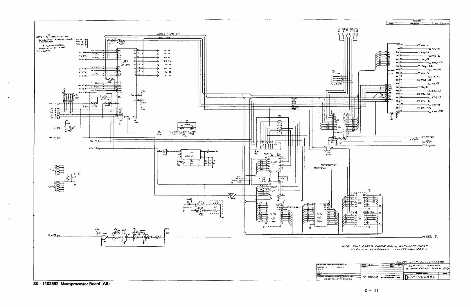
II~O _ NOTE· ~ 'M:llLA"llC'" 1;0
CJ:tHOvc,.T044. f(1~eON c:..AH..LEc. o..Jt<JE<." OA.
... t:::> 'NO\U\"'('~ CC'lNtllc..'fION ON coc£ '-I""II'JN(.C. 'top..
.... 's ~ ••• It. 110". 17 ,,",,0 Ie
ia:;::{.;· J,:::;.lAPt"
r.0 3!: '0 .. +11,,1-, .. Al
"' " Rl ",<I{--- . ' .. .~
A5. ... ' <E . ., UtI!-
-I~~ Mt.6eol.
"' ~ ... ." ... '" A" :~~ •• ~~~S~~~~~~~ .'+1~ At. .....
A' .... -,
"0 '<l A,,4-+
~"l +0 'D AI'1.
.r,.
Ao\ 46 1. A'~ AI"I"3i. A, .. +2. Ijj, ~~
3 "'" .,. ....
m -'u r -1 U14U~ ~j~~ J ,"'''1+-llOll .-L1. ... -
• -- --«.
_"I' 71."
~Q <;~I 7..0. I .~
~~: ~ 8 I 1 II :--.r ..
.r- ~ ~. l ....
... Do I .. , .. .~ ~ ~. ~ 27
p. ~"
I ;s. '<.<~
"o~e:ss .. C.TI'IL 8J~
"7'
----
tie :I. Ol '2' 02 ...
0'3-7,.
[)&.j_'I'2
DS 2..,
D ... -~
O~ ""
~
L.-n ·~~R3J ~ ;. ~...:.,~ ~[~
L _________ .... "''!~':_---''''Il~
IO~ 7+0+ ... . ~ ~Q() 7
ff. ~~<~----~------____________ -+-
A~ • -+Sv ~
1 +Sv
3 • '" G-I.f .,
1"--r'HN'---.. s.
"-U' 'fl. l'I!l!S
m
.'"~ ....... ->"' ~ ~ ~ ~
""
14"
+16 +.,.. .. S~ ~
I (.-~,,<~-i.:!_'~ ~:~~ ~ I
~::i:tk::::t::A~ o"::.!l!L. __ -' '" L..~I __ cu..
To.
~"~9~~==ti~~~~~~~==~~ • .!o<
+s"
D2 (;2 c.1 Dlet G\ Ie. 'iI~Nl1U.
~JQ Q
~~~.~' , I ' __ !:2~
r 00 ' " -DZ -:., r3 11. (-+ :.,
f L _0
" r '
..
R(VISIONS
CAt -w "":t= d CA~"'X r.. CJ f'IIszI.'l+
""1' a " .. ~-~
'.'1; ; P"1-A
"3 --::::J PI\~-'l.".!>
".,.. P,,+-2.'l.
_'M,!, ~ ws ::; a Pk.-'t 11'-1-21
,..'" f't¥ -'221
P'~-~
c ... ~-fW:iI" ~
te. I' VQA.-'f
fill " PS2 E
,e~ • P~_"l.' P
'c;..!io\
~ " .. 0>. . Un "2, RS-
PB+-'2G f'851" a Pe,5-D
'). .... 5;. r8 " P8G-~ eM 19 ~S\-f\
p&7 • pe., 2.S
u.~IT''--------<:: eel. -7.0
.~.
f1i14I:~ ======= D' --1'" ~~-tO CJ Gr,,·\-
C~-M
s· uq l~
IN, MM ~L ~~E
r ~,
~lIJtll
~\~g ,~~------" L-__________________ ~----------------~~
.~
~ -,;0 0 1''- "00 'r'\ ,
SK • 1102882 Microprocessor Board (A8)
03 10 .~
L-________________________________ r-____________ ~.jClOv~ ~~~I Ul q
r _____ ., ., '- .. 0+ • ~"'" ... ~
r. - - - - -,l!:f ... 'ff ~.:~ ba ~.,.., ~:!o o,~,
,. ."" I 1'0(1 - - - - ~. r-~.~.=j6q---~fI! .~~ ... ----
/;.~__r·-f\1.211'2. o .. ~
V1.tWC;'::' Ul. ~;:;;...-..= ~ ~ V. filS "-b~ _"'7.
"'" A1~ Po. _____ .....
- ~ .,.,. q.. .,. (]3 13 Uf> c:e818 c.~
(t ___ _
~---'~nt~ - '~~ Ufi gil
v,*-+",~;~ ~ ~ ~1 I l _____ J
'" ,- "': - , ' ;, ~"b Jrij"" 27'. • ~~~~ ,:- ,,,, ;~ f'~ ,
"- "" 1;,;.- f'"' ~ J J J _ ~ ", • ~ lOt< Cl~-\-\ "r ''-'~~1'.: ',' lJorE r#/~ .40I'1RO ~""o= FRO'"1 "",rwo-€k /='/If'.5r
{/SeO 0"-/ SC#€~.477t: ~A- 17.3080 RGII'-
-,-",.,; L/~r ,P,-5 - / -tOLl .... MCII UfiI~ISS O'"IIlWISI SHe"IID _ :~ 10" n'Ll SC ~\:"\"(\f\~\c. O\A..~ "-...fd \J\..
rMCnotI_. AIIOU,. 1"i\\C.~Of~~c!.. ¥-o"Q..o., AS --------I ~ - ~ -- ~- ... __ . ::.:,"'C~~('.. ... II~II'~~ __ '~~_'_(~' ... l ~> GOULD ___ .. _._u ___ ~_ -S't<.- /102882.
DO NOT <>CALE THIS DRAWING
c - 11
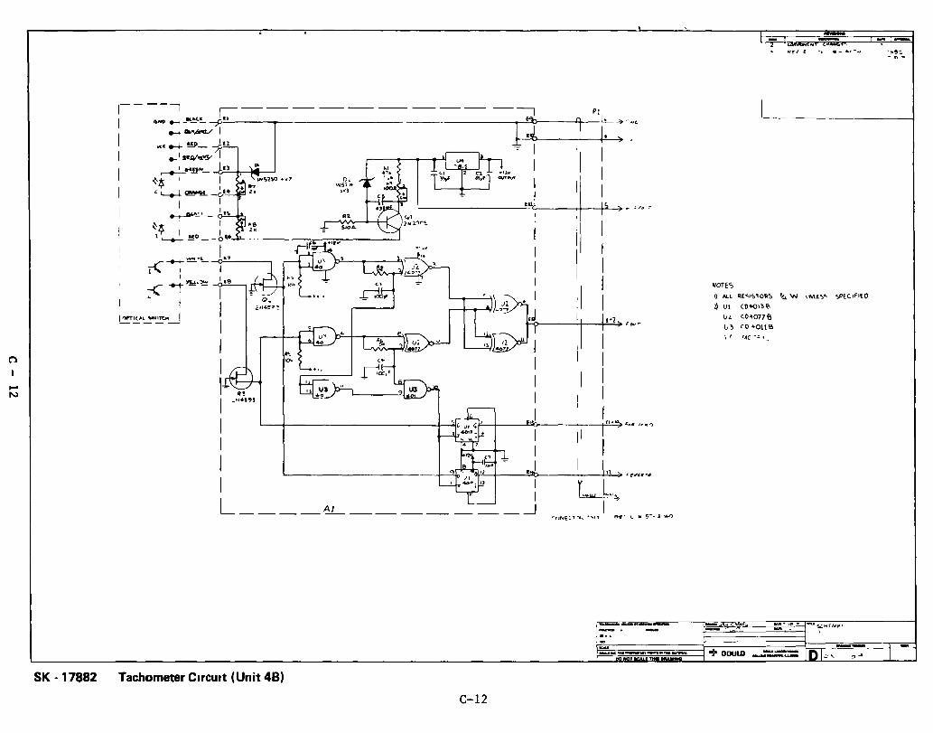
n
.... N
SK ·17882 Tachometer Circuit (Unit 48)
C-12
-~
a -=- I
I I I
tU I
Pl
9 ~""":"~AJ"
I· ) . I
I I I I
I I .. '0'0 1"
j-2 , ... -
NOTES ., All
~ VI
(J<
v~
( t
1-
ItE.c..I~"O~~
CO'<>,3 e-<..0-0776 (0 "011 B rAe -=. 1_
~W
....... , ... Mft _
-----~ o? OOULD
• -' .,-A,J
~ 'Nlf,,)' ~P~C'FltD
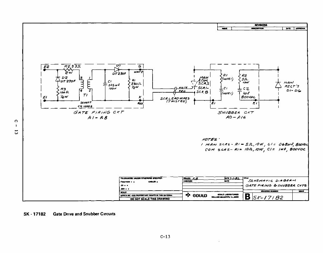
n
SK - 17182
GATE FII?/NG CKr
AI- A8
_____ D
Gate Drive and Snubber Circuits
'RAC'IIOII ••
.IX ••
JIXl ••
-. DO NOT SCALE THIS ORAWING
C-13
- 1 ..... 1-...
#orF.s . I MAIAJ ~C;f$- /?/-SJ2.,IOW I C,I= 068)A~S(J(ND'
COM SC.~5- RI= IOJ2.. I IOvtl, C/= IAlI1
800V'OC
__ k R ..... -J-/J2. mu
I-=CMKUD==-______ --= ... ::.: .. =--_---l se HE Mill rl C 01'" <!JRA ,."
GArE F/~ 'AJ6 ~ SAJIJBB~1't. CKT'S --- --> GOULD B ISK"-17 /82 T
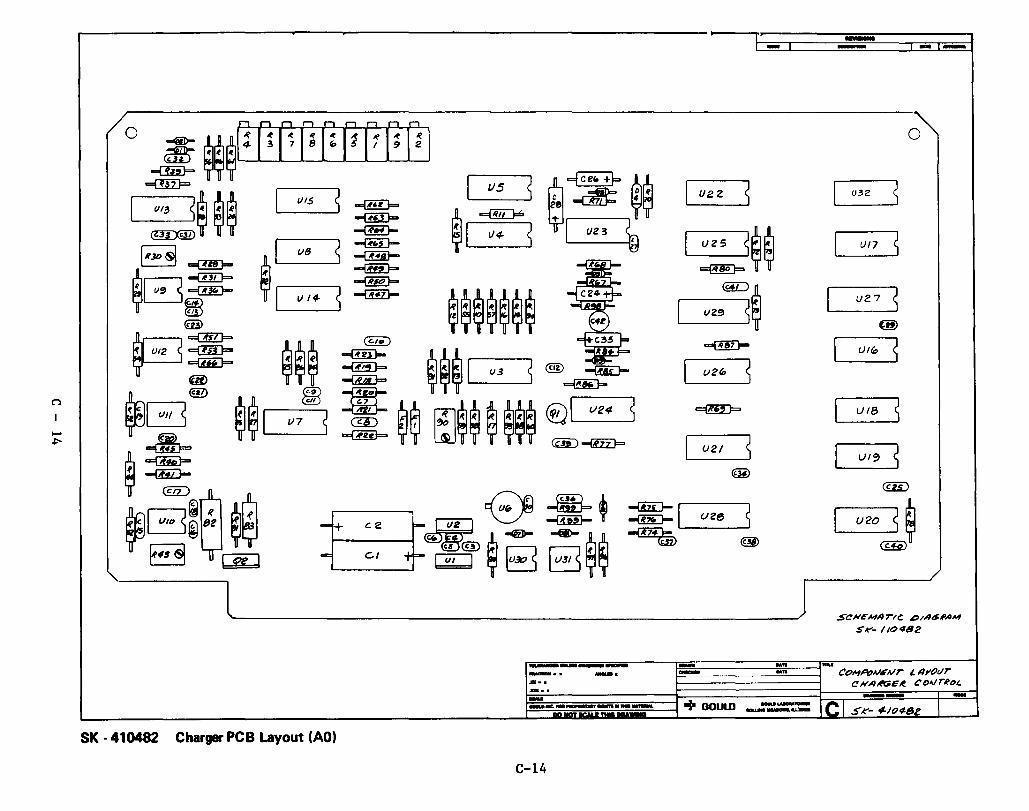
(")
I
SK ·410482 Charger PCB Layout (AO)
~.. ..... .G ••
C-14
I U2Z 5
I U21 5
+ OOUlD _-::='".:=
o
U3Z 5
1)/7 5
uz. 7 5
UI'!J 5
.sCHEMAr;~ ~;A6'1II""
SIt'- 110482
COMPtJAl6A1r L AJI()i/r CHAItGEIt. CDAlrRoL
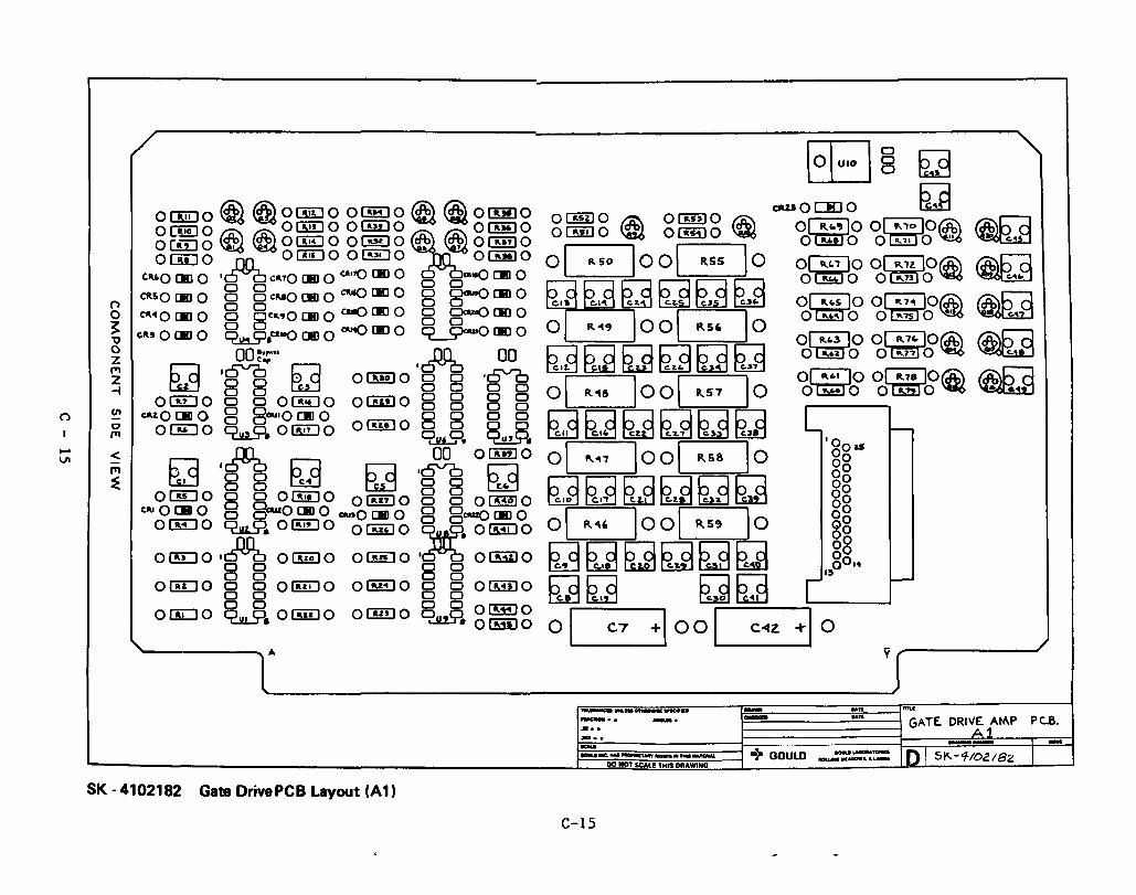
OUJDO ~ ~ 0Cii!J0 O@£)O @ @ ow!)o o ern 0 0 I3l!J 0 omuo tA::\ 0 I .... , .. 0 OWJO @ ~01IEJ0 OGElOx. ~01"S710 ocmo 0[!l!J0 [email protected] 01",.10
CI\.40 CE 0 .A C"70 lEI 0 CA.7() lEI 0 ca-o CIII 0 a a a a CflSO lEI 0 a a c .... O lEI 0 CU() IE 0 8 gCM() CIII 0
8 c ..... OIEIO 8 BI::"~oCBIo cuQlEO 8 ~[KJO ~ c: ... , 0 IE 0 ~.e.1O() CBI 0 ~o IE 0 ~o IE 0
~ 00 ~~.. 00% 00 ,., n I~ 0 ocmJo'o a 'c:5"b z t:a::1 00 ~ 00 0C)
-i 0m:J0 8 B ocmo 0(ffi)0 8 B B B ~ ~"lO CB 0 8 BCIU·o CE 0 a a a a t7 oaoo C"'LC"I OcmJO 0(lii)0 a a a a ,., ~. 0uu9. ~. < Jllo 00 0 1",,1 0
a:9 '8 8 BB M '8"8 M OC!DO a a O[§JO Olu.IO 8 8 01 ..... 010
''', 0 [II! 0 8 §ca110 CBI 0 ClUSO CB 0 8 8euzo IE 0 O(E)O ~ o~o ocm::JO ~. OWIJO
o (!DO 100% OWiJO 01,,2510 ·~o 013jl)0 o 0 a a a a a a OCll:JO a a 0CfiI]0 011U110 a a 0CEi)0 a a a a O(![]O ~d ~ OlluzlO OcmJO 9v!~ OW!JO
~. ·o~o
------_.A
SK - 4102182 Gate DrivePCB Layout (A1)
--. --. -..
C-15
o~o or;::nlo@ o~o o~o~
o~o o~otA::\ o~o 01:5r'0 ~
ortWlo o~otA::\ o~o o'"Gllr'o ~ o~o orR78lo~ o~o ol£ifo \V6
~ ~ ~ ~ ~
y ,.-______ J
GATE DRIVE. AMP P c..B.
-> GOULD
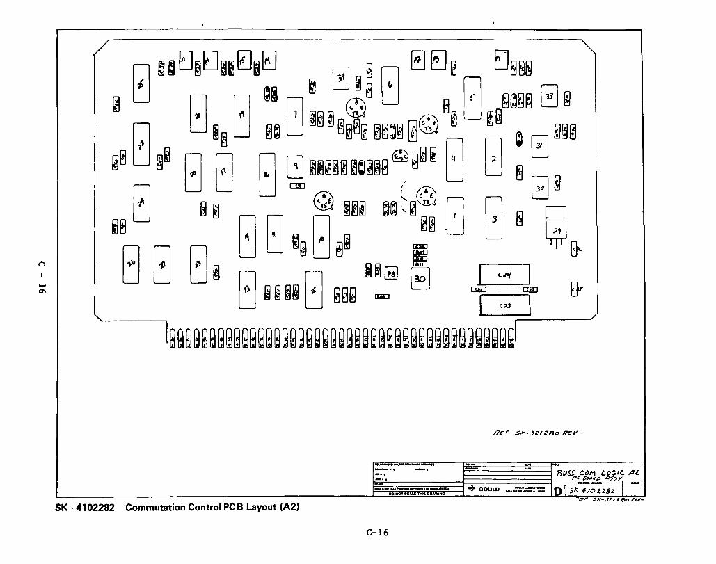
(")
I -0\
--------------
-......cD __ ......... II'fCIN:..... ." ""-I _a. __ . - ._ :::. BIJSSp/£!JbL$~/!:- ,4e MaO --- .... ,-,--,...--.. ,--
DO .OT SCALI THtS DRAWING
SK ·4102282 Commutation Control PCB layout (A2)
C-16
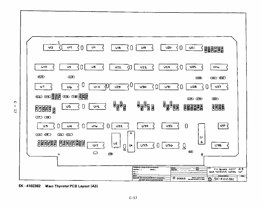
1
I \JI3 ~I I.JI'2. ~O I 1.111 ~ I UI8 ~ ° I UI9 ~ I U20 5 ° I U21 ~ ~~~~~~
I UIO ~ I U9 ~ol U8 ~ I un sO I U23 5 I \J'Z~ 5 ° I \Jzs S I U'Z,," 5 @I) ~ <ED (ill) @D
I U1 S I U~ S 0 I U\4 501 U2.9 s°l U'?lO 5 01 U~I SO I U28 5 0 I UZ1 5 ~ @D~~~ @) ~~~~ (§!) @!) CfE)
~~~~~ ~ I U5 S 0 I UI':> ~ @~~~ ~~@~ ~ ®~,~~~ ~~~~~~ ~~~~ @:>~
1 S ° I 5 0 I ~ ° I 5 I ~ I S 0 r- E3 U3 U4 UII .. U~'2. U'?>'" u35
r-
@2) @L) C§D @D
GJo +
C.I
~~~~~~ ~~~~~~~~ I I U33 S 0 I ~ I U38 UI7 S C4 U3" 5 0 5
c'" C'3
0 @ '--- <ill
"- '" y /
\ 'fOUMtCU .......... O'MliltWfll ,"C:WIID
So- .... "'u p c. &o,.ltl> A 55 i' A 3 - .. _a. .. .. .... ~"Itl ~K'I'I\I~Toli. ",.jltl4 CI:.T -.. .... , .......... .,. ... ....
eGUL • ...e MA' N.C. ... U .. II' lUG"" ... 'MI' ."UIMA&. -} GOULD .ou .. -:~:= o !SK-<;t/OZ38Z DO NOT SCALE THIS DRAWING
SK·4102382 Mam ThYrIStor PCB Layout (A3)
C-17
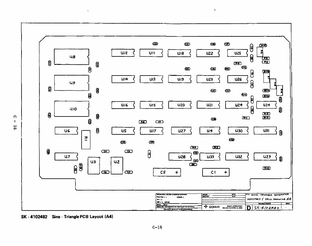
(ffi) (§i) (§I) @!)
~8 rt ~I ~ I UIZ ~ I UII ~ I ula ~ I UZZ ~ I UlS U8 8 rn:J @ CHl
® ~ C§!) @ID (ffi)
~ (I!!!
@I 1 I UI+ ~ I UI3 ~ [ UI9 ~ I Ul3 ~ I UZG l§
~I--t uS?
~-b @ @) @l)
@
uz.
8
; ~ I cml ~
~I l I UIG ~ I UlS 5 I U2.0 ~ I Ull 5 I U3+ 5 UIO ~
(t lEI)
@ C!!D lED ~ em aD
I U6
~0 ~ I us ~ I Ul7 ~ I U27 S I U4- ~ I U30 ~ I U31 ~® @!) @!)
m C!!J C!IJ
(i aD aD 8 ~@)I I U7 5 I uze U33 ~ I U3l ~ I UZ9 ~ ~ DO <®
8~ CiD
I +1 I +1 I::!ID
aD aD C5 CI
l j .. .. ft'" SINE - TlIlANGLt GENEII/l.TOII -.u.u.caL ........ 0' ....... "'"" •• ~-- .. ...... ........ .... .... ASSE:l'laLY ( DIIILL D~"WING A4-
...... 00.$ IMA ___
..... ..... I IOIIIU IIIC tIAI....."...UUY IIIO""" , .. , 1lA1I1II&l -> GOULD MLL*leo::~~ D I 5K-41021£8 Z. I -DO HOT SCALE THIS D"AWING
SK ·4102482 Sine - Triangle PCB Layout (A4)
C-18
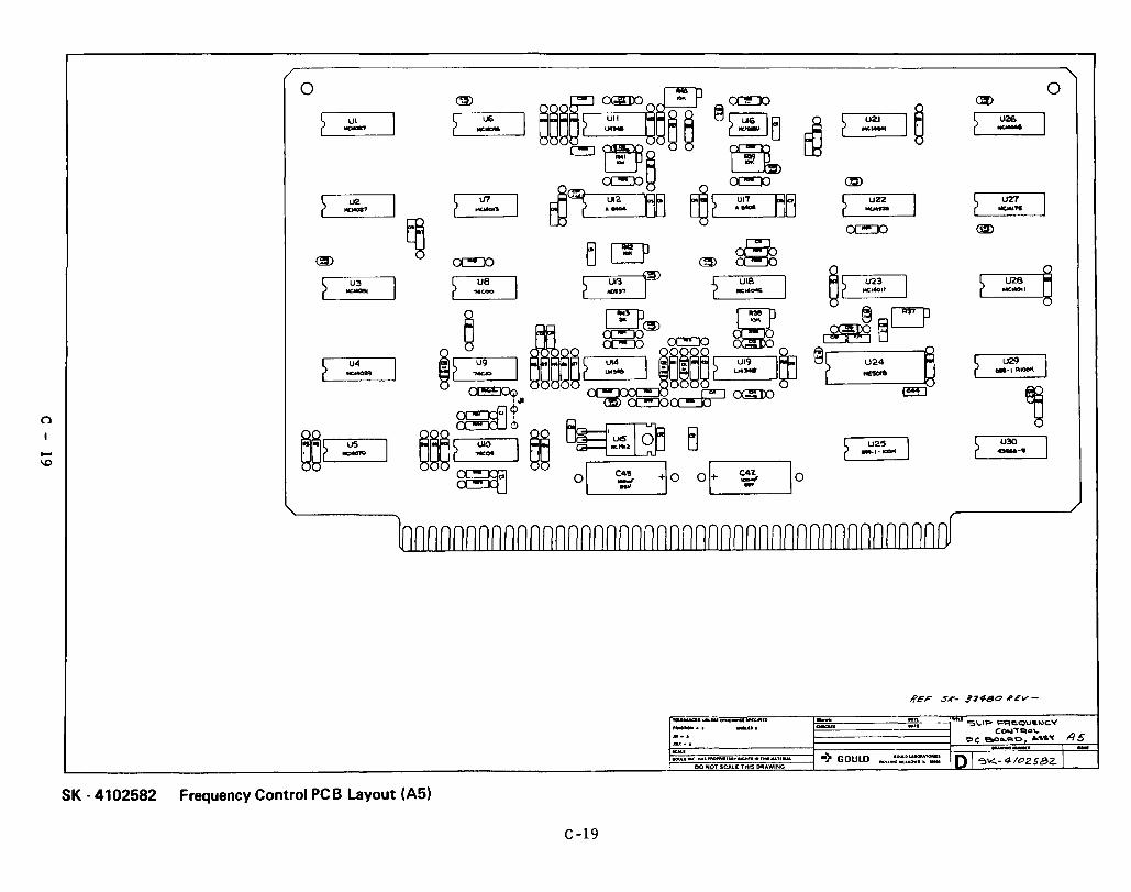
o
? ~, I
SK -4102582
o
~ ~
~ U30 r elM-IS
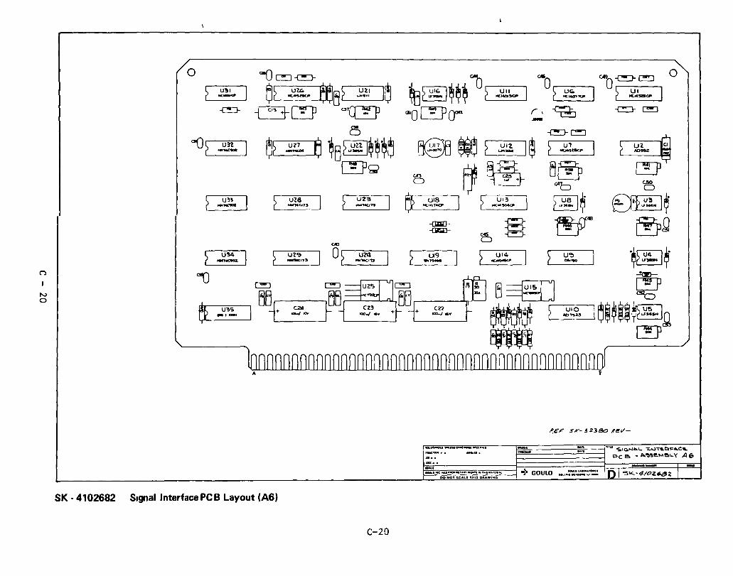
0 'iJ~~
\J§~~~ "b f .~~ I CA50 ""0 ~ ~ 0
~ U31 I e? Uu. eeB? UII I~ ~ ~,:,.lU' I ? ~J_ao I IIIC_I(P ""'"~ l,.Io4e ..
-e:::J- C3-c:J 01Q!J a.O~oon (, ~ -c:J- ~ -0 ~~
1J~ un ~? UZ7 e ~B~~~~~ f@j~ ? Ull. I@ ~ U1 cg -- ..- LM ..... _.-.. 100562 _
[!}lQ CA3 ~ ~~~ ~® L:]J 0 c..!5O
~ 0
? u~~ ? uZ8 ? u'Z~ ~ UI8 I ? UI3 I ~~ €Jf,~':'·I~ ... ~ ........ qf~ --...,. Mi:.I.,l<&(P "","5OO(JO
-{JI;Ij/]- ~ &43 ~cO -{W}-- ~ '45 ~ 0
CAl
~ ~I ? ul~ I O2 u14 ~ Vol£!. I ~ ~~ I ~ U~ .~~~. ....... 1'3 "''NC..13 ~, ....
('") au ~
~ ~ I~I J [!} N
I ~B+ CU 0 a ~~$ IO~~~@~~~ u~s C2A
~ UIO .. ,- ..., ... 1Q"'5Z3
~ ~
:::: - ,.,~. c;.Ica....a .. I.... "l:.'-l'Te:.Q~ ... C'" PC eo. - ~"Y3t!.Me.I..'( A Eo
-. __ .... _IIIf"'.y_ .. ,. ... , ... , ... ,(..... -> GOULD "' .... ~:=:.:: NOT SCAlf THIS D""'WING
SK - 4102682 Signal Interface PCB Layout (A6)
C-20
(")
N -
I ,......,
( - +- JI
I c:=- C'.
ctOc=o ~
U'Go UI4
- "'--~ c,~
---/"\...-
u,~
G "
\..
I
SK ·4102882 Microprocess Board PCB Layout (A8)
-
\
::::: e El 8 B c .. ""'" {EJ---- .Ju'
CI~-- ~ ~ - - - oJ",,"
C" c:::::II -GW---- ....,.
G 6 --- ..... - -- ..au ... - - - .we;. --- "u.., --- ,Ju.
--- Jtu,
c:=- c,z.
B B
... -...cu -.1 .. 01 ........ "'" ......
PMC1'IOII ... _ ... -.. ...... .....
..,.. • ..:ItAI-'OOO ... , __ " ... , ..... " .. iU.
DO NOT SCALE THI$ DAAWING
('-71
I I
- +---'
I '!>I
c::=:::IIC11 .-cw
uc;, us
" ---..r......
""'" <;10 _c,
G G - c. -'"
B .. 0 +
= ~
CI
c.. = 1+ ~ ct T cc;, T
./
ReF s"K-.3Z1 180 .lEv-
- un "'" ""\CClO"''''OC.e.~SOt:l COIIua .. n
~ c e.o ...... o. "'li~'(' A8
roT S:--;';~e8Z I --> GOULO _.~,_u
_~_ ... _ ... u_
A
ac
o
dc
Es
gm
hp
Hz
Ipk
1m
Kc
kg
kW
km/h
L
LSTRAY lbs
m
MPH
N-M
NA
NB
PLOSS
POUT PWM
Q
RMS
7. DEFINITIONS
- Amps
- Alternating Current
- Commutation Circuit Total Capacitance
- Circuit Breaker
- Charger Total Resonant Circuit Capacitance
- Degrees Centigrade
- Silicon Rectifier
- Direct Current
Commutation Circuit Stored Energy
- Grams
- Horsepower
- Hertz
- Peak Motor Line Current
- Peak Resonant Circuit Current - Charger Operation
- T1A Winding Current When 07 Forward-Biased
- Inches
- Resonant Circuit Loss Factor
- Kilograms
- Kilowatts
- Kilometers/hour
- Commutation Circuit Inductance (T1A Winding)
- Commutation Circuit Stray Inductance
- Pounds
- Meters
- Miles/hour
- Newton - Meters
- Number of Turns (A Winding)
- Number of Turns (B Winding)
- Charger Power Loss
- Charger Output Power
- Pulse-Width-Modulation
- Quality Factor
- Root-Mean-Square
7 - 1
Rad
SCR
S~
T
trev
VB
V~
VC4
- Radians
- Silicon-Controlled Rectifier
- Society of Automotive Engineers
- Commutation Transformer
- Reverse-Bias Time Applied to Main Thyristor
- Propulsion Battery Voltage
- Commutation Capacitor Initial Voltage
- Input Line Capacitor Voltage
- Angle at Which D7 Forward-Biased
- Charger Efficiency
7 - 2
8. REFERENCES
1) T. S. Latos, "Improved SCR AC Motor Inverter for Battery Powered
Urban Elec tnc Vehicles," F~na1 Report Contract DOE/NASA/0060-82/I,
December 1982.
2) S.C. Peak, "Improved Transistor1Zed AC Motor Inverter for Battery
Powered Urban Electr~c Passenger Vehicles," Final Report Contract
DOE/NASA/0059-82/1, September 1982.
3) S. Geppert, "AC Propuls~on system for an electric vehicle," Final
Report Contract DOE/NASA/0125-1, August 1981.
4) A. Abbondant~ and P. Wood, "A cr~ter~on for performance comparison
between high power inverter circu~ts," IEEE Transactions on Industry
Applications, pp. 154-160, March/April 1977.
5) S.B. Dewan and D.L. Duff, "Opt~mum design of an input commutation
inverter for ac motor control," IEEE Transactions on Industry and
General Applicat~on8, pp. 699-705, Nov/Dec 1969.
6) R.M. Davis, "Power Diode and Thyristor Circuits," IEEE Monograph
Series 7, Copyright 1971, Peter Pereguness LTD Publisher.
7) W.E. R~ppel, "Optimizing Boost Chopper Charger Design, "Proceedings
of Powercon 6, May 1979.
8) J.M.D. Murphy, "Thyristor Control of AC Motors," Pergamon Press,
Copyright 1973.
9) D.A. Bradley, C.D. Clarke, R.M. Davis, D.A. Jones, "Adjustable
frequency inverters and their application to variable speed driver,"
Proc. lEE, VOC III No. 11, November 1964.
8-1
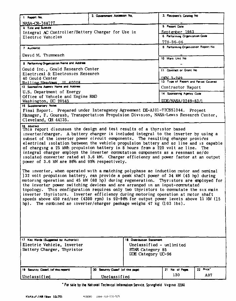
1 Repon No.
NASA-cR-16S177 4 Tltl, and Sublltl'
2, GCMrMIIftt Ace.." No, 3, RICIPtIfII'S c.talog No
5 Reoon 0111
Seotmner 1983 Integral AC COntroller/Battery Charger for Use in Electric Vehicles 6 Performing OrCjlmlitlon Code
778-36-06
7 AuthOr!s' 8 Performing Orljlnilition Report No
David M. Thlmmesch ~---------------------------1 10 Work Unit No
9 Pwfarml"9 Orgllliution Nlme and Addr_
Gould Inc., Gould Research Center Electrical & Electronics Research
11 Contrle! or Grlnt No
40 Gould Center nm~-?~Q ~~Rt~,n'~lLl~i~n~"~~~~o.,a~,~~~~u~~_~"I~~~:n~ln~lln~1'Q~ ______________ ~13 Ty~~R~~dP~~Co~~
12 SoonIorlna ~v Name and Addr_ Contractor Report U.S. Department of Energy 14 Soonsorlng Agencv Code
Office of Vehicle and Engine R&D Washington, DC 20545 JX>ELNASA/0249-83 11 15 Suppl,mentary NottS
Final Report. Prepared under Interagency Agreement DE-AIOl-77CS51044. Project ~~nager, F. Gourash, Transportation Propulsion DiVISion, NASA-LewiS Research Center, Cleveland, OR 44135. 16 Abstrlct This report discusses the design and test results of a thyristor based Inverter/charger. A battery charger is included integral to the inverter by using a I subset of the inverter power circuit components. The resulting charger provices electrical Isolation between the vehicle propulsion battery and ac line and IS capable of charging a 25 ~ propulsion battery in 8 hours fram a 220 volt ac line. The integral charger employs the inverter commutation components as a resonant ac/dc Isolated converter rated at 3.6~. Charger efficiency and power factor at an output power of 3.6 ~ are 8~ and 9~ respectively.
The Inverter, when operated With a matching polyphase ac induction motor and naminal ]32 volt propulsion battery, can provide a peak shaft power of 34 ~ (45 hp) during motoring operation and 45 ~ (60 hp) during regeneration. Thyristors are employed for the inverter power switching devices and are arranged In an input-cammutated topology. This configuration requires only two thyristors to commutate the SIX main inverter thyristors. Inverter efficiency during motoring operation at motor shaft speeds above 450 rad/sec (4300 rpm) is 92-9~ for output p~ver levels above 11 I~ (15 hp). The combined ac Inverter/charger package weighs 47 kg (103 lbs).
17 Key Wordl ISutIJIIUd by Author!s ••
Electric Vehicle, Inverter Battery Charger, Thyristor
Unclassified
18 Oll1rlbullon Statement
Unclassified - unlimited STAR Category 85 I:oE category UC-96
20 Secunty 0-' 10' I"" PIlI'
Unclassified
21 No of PICJII
130
• FOI sale by the National Technical InfOlmatlon Service. Springfield Vuglnla Z2161
NUAJ".16llR_ 10-75) *USGPO 19&4-759-100-525
22 PrIC'·
A07

End of Document


![IMN605 Motor CC de Potencia [HP] Integral](https://img.pdfslide.net/doc/110x75/619c52e269476666743e0fd0/imn605-motor-cc-de-potencia-hp-integral.jpg)


![Telemecanique Integral 32 Motor Starter[1]](https://img.pdfslide.net/doc/110x75/547733cdb4af9f81108b4695/telemecanique-integral-32-motor-starter1.jpg)