Embed Size (px)
Citation preview
KSZ8864CNX/RMNUB Integrated 4-Port 10/100 Managed Switch
with Two MACs MII or RMII Interfaces
Revision 1.5
LinkMD is a registered trademark of Micrel, Inc.
Micrel Inc. • 2180 Fortune Drive • San Jose, CA 95131 • USA • tel +1 (408) 944-0800 • fax + 1 (408) 474-1000 • http://www.micrel.com
October 26, 2015 Revision 1.5
General Description The KSZ8864CNX/RMNUB is a highly-integrated, Layer 2-managed 4-port switch with optimized design, plentiful features and smallest package size. It is designed for cost-sensitive 10/100Mbps 4-port switch systems with on-chip termination, lowest-power consumption, and small package to save system cost. It has 1.4Gbps high-performance memory bandwidth, shared memory-based switch fabric with full non-blocking configuration. It also provides an extensive feature set such as the power management, programmable rate limiting and priority ratio, tag/port-based VLAN, packet filtering, quality-of-service (QoS), four queue prioritization, management interface, MIB counters. Port 3 and Port 4 support either MII or RMII interfaces with SW3-MII/RMII and SW4-MII/RMII (see Functional Diagram) for KSZ8864CNX/RMNUB data interface. An industrial temperature-grade version of the KSZ8864CNXIA and a qualified AEC-Q100 Automotive version of the KSZ8864RMNUB are also available (see the Ordering Information section).The KSZ8864CNX/RMNUB provides multiple CPU control/data interfaces to effectively address both current and emerging fast Ethernet applications.
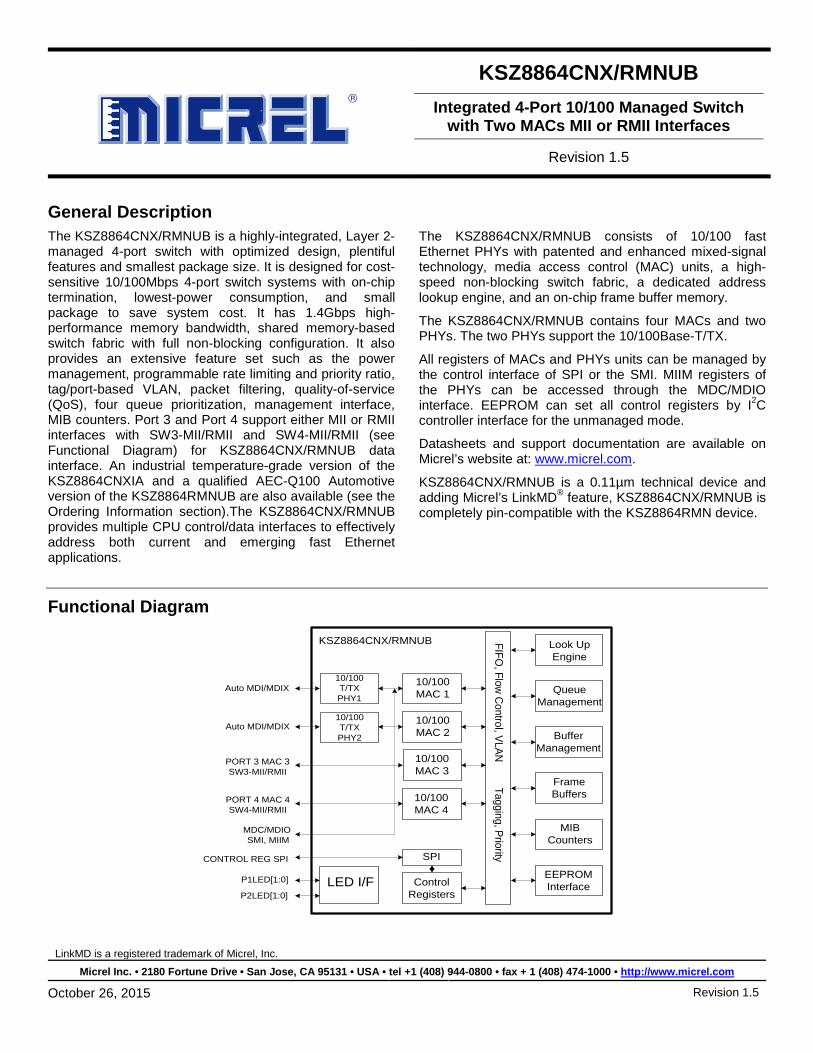
The KSZ8864CNX/RMNUB consists of 10/100 fast Ethernet PHYs with patented and enhanced mixed-signal technology, media access control (MAC) units, a high-speed non-blocking switch fabric, a dedicated address lookup engine, and an on-chip frame buffer memory.
The KSZ8864CNX/RMNUB contains four MACs and two PHYs. The two PHYs support the 10/100Base-T/TX.
All registers of MACs and PHYs units can be managed by the control interface of SPI or the SMI. MIIM registers of the PHYs can be accessed through the MDC/MDIO interface. EEPROM can set all control registers by I2C controller interface for the unmanaged mode.
Datasheets and support documentation are available on Micrel’s website at: www.micrel.com.
KSZ8864CNX/RMNUB is a 0.11µm technical device and adding Micrel’s LinkMD® feature, KSZ8864CNX/RMNUB is completely pin-compatible with the KSZ8864RMN device.
Functional Diagram
Look Up Engine
QueueManagement
FIFO, Flow
Control, VLAN
Tagging, Priority
SPI
EEPROMInterface
LED I/F
CONTROL REG SPI
MIBCounters
P1LED[1:0]
P2LED[1:0] Control
Registers
MDC/MDIO SMI, MIIM
PORT 4 MAC 4SW4-MII/RMII
Auto MDI/MDIX
Auto MDI/MDIX
PORT 3 MAC 3SW3-MII/RMII
10/100T/TXPHY2
10/100T/TXPHY1
10/100MAC 1
10/100MAC 2
10/100MAC 3
10/100MAC 4
BufferManagement
FrameBuffers
KSZ8864CNX/RMNUB
Micrel, Inc. KSZ8864CNX/RMNUB
October 26, 2015 2 Revision 1.5
Features Advanced Switch Features • IEEE 802.1q VLAN support for up to 128 VLAN groups
(full-range 4096 of VLAN IDs). • Static MAC table supports up to 32 entries. • VLAN ID tag/untagged options, per port basis. • IEEE 802.1p/q tag insertion or removal on a per port basis
based on ingress port (egress). • Programmable rate limiting at the ingress and egress on a
per port basis. • Jitter-free per packet based rate limiting support. • Broadcast storm protection with percentage control (global
and per port basis). • IEEE 802.1d rapid spanning tree protocol RSTP support. • Tail tag mode (1 byte added before FCS) support at Port 4
to inform the processor which ingress port receives the packet.
• 1.4Gbps high-performance memory bandwidth and shared memory based switch fabric with fully non-blocking configuration.
• Dual MII/RMII with MAC 3 SW3-MII/RMII and MAC 4 SW4-MII/RMII interfaces.
• Enable/Disable option for huge frame size up to 2000 Bytes per frame.
• IGMP v1/v2 snooping (Ipv4) support for multicast packet filtering.
• IPv4/IPv6 QoS support. • Support unknown unicast/multicast address and unknown
VID packet filtering. • Self-address filtering.
Comprehensive Configuration Register Access • Serial management interface (MDC/MDIO) to all PHYs
registers and SMI interface (MDC/MDIO) to all registers. • High-speed SPI (up to 25MHz) and I2C master Interface to
all internal registers. • I/0 pins strapping and EEPROM to program selective
registers in unmanaged switch mode. • Control registers configurable on the fly (port-priority,
802.1p/d/q, AN…).
QoS/CoS Packet Prioritization Support • Per port, 802.1p and DiffServ-based. • 1/2/4-queue QoS prioritization selection. • Programmable weighted fair queuing for ratio control. • Re-mapping of 802.1p priority field per port basis.
Integrated 4-Port 10/100 Ethernet Switch • New generation switch with five MACs and five PHYs that
are fully compliant with the IEEE 802.3u standard. • Non-blocking switch fabric assures fast packet delivery by
utilizing a 1K MAC address lookup table and a store-and-forward architecture.
• On-chip 64Kbyte memory for frame buffering (not shared with 1K unicast address table).
• Full-duplex IEEE 802.3x flow control (PAUSE) with force mode option.
• Half-duplex back pressure flow control. • HP Auto MDI/MDI-X and IEEE Auto crossover support. • LinkMD® TDR-based cable diagnostics to identify faulty
copper cabling. • MII interface of MAC supports both MAC mode and PHY
mode. • Per port LED Indicators for link, activity, and 10/100 speed. • Register port status support for link, activity, full/half duplex
and 10/100 speed. • On-chip terminations and internal biasing technology for
cost down and lowest power consumption.
Switch Monitoring Features • Port mirroring/monitoring/sniffing: ingress and/or egress
traffic to any port or MII/RMII. • MIB counters for fully-compliant statistics gathering 34 MIB
counters per port. • Loop-back support for MAC, PHY, and remote diagnostic
of failure. • Interrupt for the link change on any ports.
Low-Power Dissipation • Full-chip software power-down and per port software power
down. • Energy-detect mode support <0.1W full-chip power
consumption when all ports have no activity. • Very-low full-chip power consumption (~0.3W), without
extra power consumption on transformers. • Dynamic clock tree shutdown feature. • Voltages: − Analog VDDAT 3.3V only. − VDDIO support 3.3V, 2.5V, and 1.8V. − Low 1.2V core power. − 0.11µm CMOS technology.
• Commercial temperature range: 0°C to +70°C. • Industrial temperature range: –40°C to +85°C. • Available in 64-pin QFN, lead-free small package.
Micrel, Inc. KSZ8864CNX/RMNUB
October 26, 2015 3 Revision 1.5
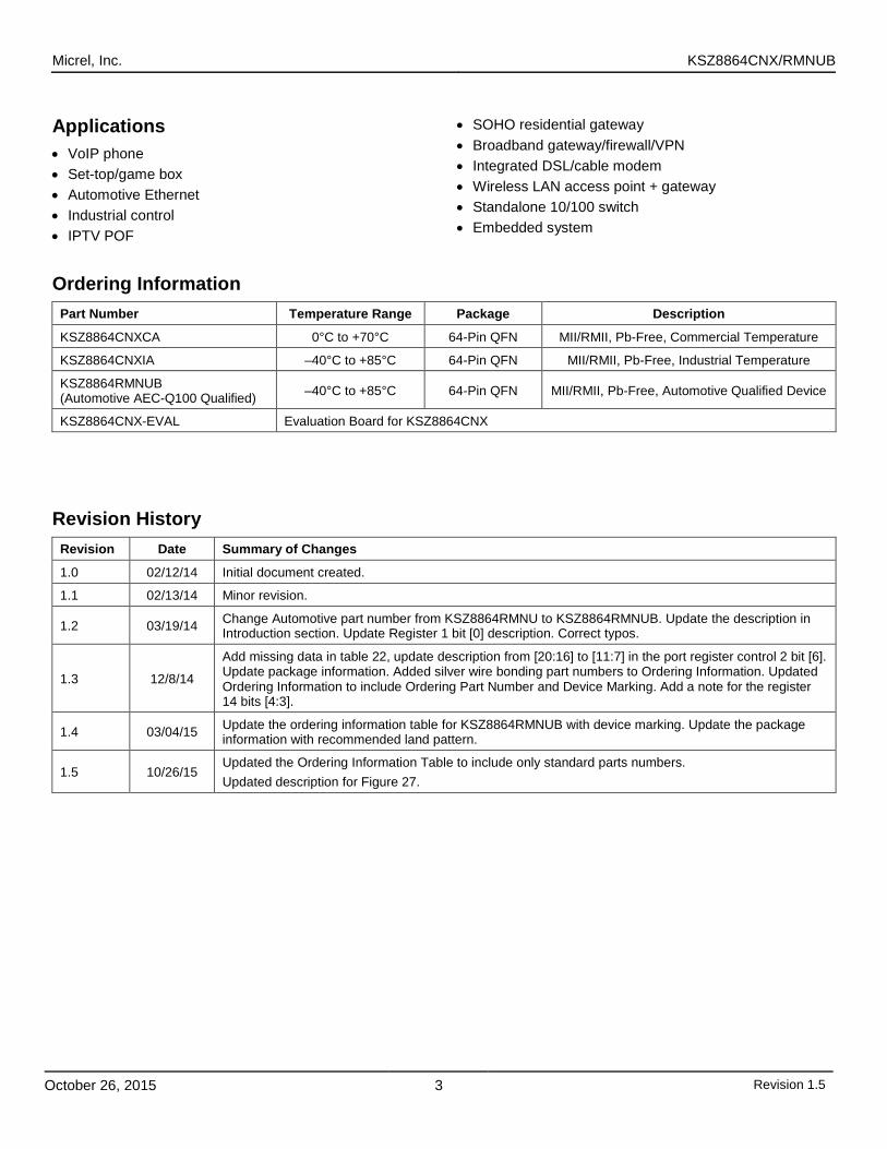
Applications • VoIP phone • Set-top/game box • Automotive Ethernet • Industrial control • IPTV POF
• SOHO residential gateway • Broadband gateway/firewall/VPN • Integrated DSL/cable modem • Wireless LAN access point + gateway • Standalone 10/100 switch • Embedded system
Ordering Information Part Number Temperature Range Package Description
KSZ8864CNXCA 0°C to +70°C 64-Pin QFN MII/RMII, Pb-Free, Commercial Temperature
KSZ8864CNXIA –40°C to +85°C 64-Pin QFN MII/RMII, Pb-Free, Industrial Temperature
KSZ8864RMNUB (Automotive AEC-Q100 Qualified) –40°C to +85°C 64-Pin QFN MII/RMII, Pb-Free, Automotive Qualified Device
KSZ8864CNX-EVAL Evaluation Board for KSZ8864CNX
Revision History Revision Date Summary of Changes
1.0 02/12/14 Initial document created.
1.1 02/13/14 Minor revision.
1.2 03/19/14 Change Automotive part number from KSZ8864RMNU to KSZ8864RMNUB. Update the description in Introduction section. Update Register 1 bit [0] description. Correct typos.
1.3 12/8/14
Add missing data in table 22, update description from [20:16] to [11:7] in the port register control 2 bit [6]. Update package information. Added silver wire bonding part numbers to Ordering Information. Updated Ordering Information to include Ordering Part Number and Device Marking. Add a note for the register 14 bits [4:3].
1.4 03/04/15 Update the ordering information table for KSZ8864RMNUB with device marking. Update the package information with recommended land pattern.
1.5 10/26/15 Updated the Ordering Information Table to include only standard parts numbers. Updated description for Figure 27.
Micrel, Inc. KSZ8864CNX/RMNUB
October 26, 2015 4 Revision 1.5
Contents List of Figures .......................................................................................................................................................................... 6 List of Tables ........................................................................................................................................................................... 7 Pin Configuration ..................................................................................................................................................................... 8 Pin Description ........................................................................................................................................................................ 9 Pin for Strap-In Options ......................................................................................................................................................... 13 Introduction ............................................................................................................................................................................ 16 Functional Overview: Physical Layer Transceiver ................................................................................................................ 16
100BASE-TX Transmit ...................................................................................................................................................... 16 100BASE-TX Receive ....................................................................................................................................................... 16 PLL Clock Synthesizer ...................................................................................................................................................... 16 Scrambler/De-Scrambler (100BASE-TX only) .................................................................................................................. 16 10BASE-T Transmit ........................................................................................................................................................... 17 10BASE-T Receive ............................................................................................................................................................ 17 MDI/MDI-X Auto Crossover ............................................................................................................................................... 17 Auto-Negotiation ................................................................................................................................................................ 19 LinkMD® Cable Diagnostics ............................................................................................................................................... 21 On-Chip Termination Resistors ......................................................................................................................................... 22
Functional Overview: Power Management ........................................................................................................................... 23 Normal Operation Mode .................................................................................................................................................... 23 Energy Detect Mode .......................................................................................................................................................... 23 Soft Power-Down Mode ..................................................................................................................................................... 24 Power Saving Mode .......................................................................................................................................................... 24 Port-Based Power-Down Mode ......................................................................................................................................... 24
Functional Overview: Switch Core ........................................................................................................................................ 24 Address Look-Up ............................................................................................................................................................... 24 Learning ............................................................................................................................................................................. 24 Migration ............................................................................................................................................................................ 24 Aging .................................................................................................................................................................................. 24 Forwarding ......................................................................................................................................................................... 25 Switching Engine ............................................................................................................................................................... 25 Media Access Controller (MAC) Operation ....................................................................................................................... 25 Inter-Packet Gap (IPG) ...................................................................................................................................................... 25 Back-off Algorithm ............................................................................................................................................................. 25 Late Collision ..................................................................................................................................................................... 25 Illegal Frames .................................................................................................................................................................... 25 Flow Control ...................................................................................................................................................................... 25 Half-Duplex Back Pressure ............................................................................................................................................... 28 Broadcast Storm Protection............................................................................................................................................... 28 MII Interface Operation ...................................................................................................................................................... 28 Switch MAC3/MAC4 SW3/SW4-MII Interface ................................................................................................................... 28 Switch MAC3/MAC4 SW3/SW4-RMII Interface ................................................................................................................ 30
Advanced Functionality ......................................................................................................................................................... 31 QoS Priority Support .......................................................................................................................................................... 31 Spanning Tree Support ..................................................................................................................................................... 32 Rapid Spanning Tree Support ........................................................................................................................................... 33 Tail Tagging Mode ............................................................................................................................................................. 34 IGMP Support .................................................................................................................................................................... 35 Port Mirroring Support ....................................................................................................................................................... 35 VLAN Support .................................................................................................................................................................... 35 Rate Limiting Support ........................................................................................................................................................ 36 Ingress Rate Limit .............................................................................................................................................................. 36 Egress Rate Limit .............................................................................................................................................................. 37 Transmit Queue Ratio Programming ................................................................................................................................. 37 Filtering for Self-Address, Unknown Unicast/Multicast Address and Unknown VID Packet/IP Multicast ......................... 37
Micrel, Inc. KSZ8864CNX/RMNUB
October 26, 2015 5 Revision 1.5
Configuration Interface ...................................................................................................................................................... 37 SPI Slave Serial Bus Configuration ................................................................................................................................... 38 MII Management Interface (MIIM) ..................................................................................................................................... 41 Serial Management Interface (SMI) .................................................................................................................................. 41
Register Descriptions ............................................................................................................................................................ 43 Global Registers ................................................................................................................................................................ 44 Port Registers .................................................................................................................................................................... 54 Advanced Control Registers .............................................................................................................................................. 64 Data Rate Selection in 100BT ........................................................................................................................................... 79 Data Rate Selection in 10BT ............................................................................................................................................. 80
Static MAC Address Table .................................................................................................................................................... 82 VLAN Table ........................................................................................................................................................................... 84 Dynamic MAC Address Table ............................................................................................................................................... 87 MIB (Management Information Base) Counters ................................................................................................................... 88
For Port 1 ........................................................................................................................................................................... 88 For Port 2, the base is 0x40, same offset definition (0x40-0x5f) ....................................................................................... 89 For Port 3, the base is 0x60, same offset definition (0x60-0x7f) ....................................................................................... 89 For Port 4, the base is 0x80, same offset definition (0x80-0x9f) ....................................................................................... 89 All Ports Dropped Packet MIB Counters ........................................................................................................................... 89 Format of “All Dropped Packet” MIB Counter.................................................................................................................... 89
MIIM Registers ...................................................................................................................................................................... 91 Absolute Maximum Ratings .................................................................................................................................................. 95 Operating Ratings ................................................................................................................................................................. 95 Electrical Characteristics ....................................................................................................................................................... 95 Timing Diagrams ................................................................................................................................................................... 97
EEPROM Timing ............................................................................................................................................................... 97 MII Timing .......................................................................................................................................................................... 98 RMII Timing ..................................................................................................................................................................... 100 SPI Timing ....................................................................................................................................................................... 101 Auto-Negotiation Timing .................................................................................................................................................. 103 MDC/MDIO Timing .......................................................................................................................................................... 104 Reset Timing ................................................................................................................................................................... 105 Reset Circuit Diagram ..................................................................................................................................................... 106
Selection of Isolation Transformer ...................................................................................................................................... 107 Selection of Transformer Vendors ................................................................................................................................... 107 Selection of Reference Crystal ........................................................................................................................................ 107
Package Information ........................................................................................................................................................... 108
Micrel, Inc. KSZ8864CNX/RMNUB
October 26, 2015 6 Revision 1.5
List of Figures Figure 1. Typical Straight Cable Connection ...................................................................................................................... 18 Figure 2. Typical Crossover Cable Connection .................................................................................................................. 19 Figure 3. Auto-Negotiation .................................................................................................................................................. 20 Figure 4. Destination Address Look-up Flow Chart – Stage 1 ............................................................................................ 26 Figure 5. Destination Address Resolution Flow Chart – Stage 2 ........................................................................................ 27 Figure 6. 802.1p Priority Field Format ................................................................................................................................ 32 Figure 7. Tail Tag Frame Format ........................................................................................................................................ 34 Figure 8. KSZ8864CNX/RMNUB EEPROM Configuration Timing Diagram ...................................................................... 38 Figure 9. SPI Write Data Cycle ........................................................................................................................................... 39 Figure 10. SPI Read Data Cycle ........................................................................................................................................... 39 Figure 11. SPI Multiple Write ................................................................................................................................................ 40 Figure 12. SPI Multiple Read ................................................................................................................................................ 40 Figure 13. EEPROM Interface Input Receive Timing Diagram ............................................................................................. 97 Figure 14. EEPROM Interface Output Transmit Timing Diagram ......................................................................................... 97 Figure 15. MAC Mode MII Timing – Data Received from MII ............................................................................................... 98 Figure 16. MAC Mode MII Timing – Data Transmitted from MII ........................................................................................... 98 Figure 17. PHY Mode MII Timing – Data Received from MII ................................................................................................ 99 Figure 18. PHY Mode MII Timing – Data Transmitted from MII ............................................................................................ 99 Figure 19. RMII Timing – Data Received from RMII ........................................................................................................... 100 Figure 20. RMII Timing – Data Transmitted to RMII ........................................................................................................... 100 Figure 21. SPI Input Timing ................................................................................................................................................ 101 Figure 22. SPI Output Timing.............................................................................................................................................. 102 Figure 23. Auto-Negotiation Timing .................................................................................................................................... 103 Figure 24. MDC/MDIO Timing ............................................................................................................................................. 104 Figure 25. Reset Timing ...................................................................................................................................................... 105 Figure 26. Recommended Reset Circuit ............................................................................................................................. 106 Figure 27. Recommended Circuit for Interfacing with CPU/FPGA Reset ........................................................................... 106
Micrel, Inc. KSZ8864CNX/RMNUB
October 26, 2015 7 Revision 1.5
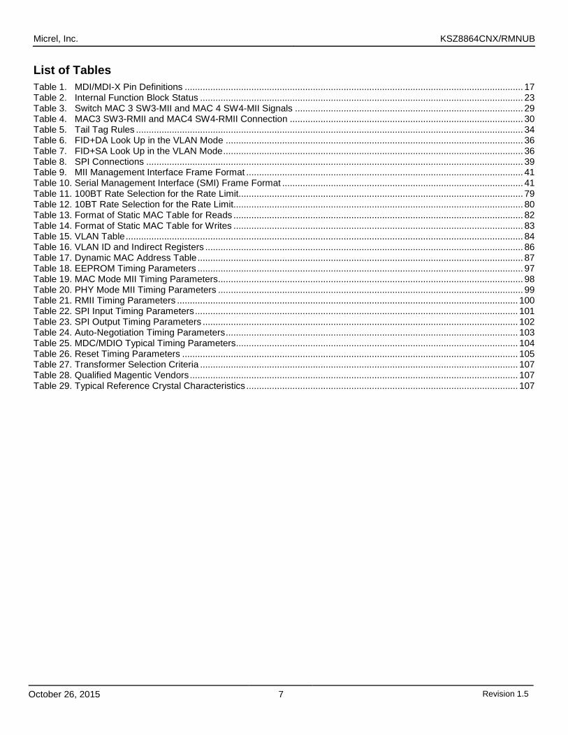
List of Tables Table 1. MDI/MDI-X Pin Definitions .................................................................................................................................... 17 Table 2. Internal Function Block Status .............................................................................................................................. 23 Table 3. Switch MAC 3 SW3-MII and MAC 4 SW4-MII Signals ......................................................................................... 29 Table 4. MAC3 SW3-RMII and MAC4 SW4-RMII Connection ........................................................................................... 30 Table 5. Tail Tag Rules ....................................................................................................................................................... 34 Table 6. FID+DA Look Up in the VLAN Mode .................................................................................................................... 36 Table 7. FID+SA Look Up in the VLAN Mode ..................................................................................................................... 36 Table 8. SPI Connections ................................................................................................................................................... 39 Table 9. MII Management Interface Frame Format ............................................................................................................ 41 Table 10. Serial Management Interface (SMI) Frame Format .............................................................................................. 41 Table 11. 100BT Rate Selection for the Rate Limit............................................................................................................... 79 Table 12. 10BT Rate Selection for the Rate Limit................................................................................................................. 80 Table 13. Format of Static MAC Table for Reads ................................................................................................................. 82 Table 14. Format of Static MAC Table for Writes ................................................................................................................. 83 Table 15. VLAN Table ........................................................................................................................................................... 84 Table 16. VLAN ID and Indirect Registers ............................................................................................................................ 86 Table 17. Dynamic MAC Address Table ............................................................................................................................... 87 Table 18. EEPROM Timing Parameters ............................................................................................................................... 97 Table 19. MAC Mode MII Timing Parameters ....................................................................................................................... 98 Table 20. PHY Mode MII Timing Parameters ....................................................................................................................... 99 Table 21. RMII Timing Parameters ..................................................................................................................................... 100 Table 22. SPI Input Timing Parameters .............................................................................................................................. 101 Table 23. SPI Output Timing Parameters ........................................................................................................................... 102 Table 24. Auto-Negotiation Timing Parameters .................................................................................................................. 103 Table 25. MDC/MDIO Typical Timing Parameters .............................................................................................................. 104 Table 26. Reset Timing Parameters ................................................................................................................................... 105 Table 27. Transformer Selection Criteria ............................................................................................................................ 107 Table 28. Qualified Magentic Vendors ................................................................................................................................ 107 Table 29. Typical Reference Crystal Characteristics .......................................................................................................... 107
Micrel, Inc. KSZ8864CNX/RMNUB
October 26, 2015 8 Revision 1.5
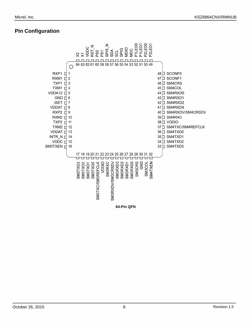
Pin Configuration
64-Pin QFN
Micrel, Inc. KSZ8864CNX/RMNUB
October 26, 2015 9 Revision 1.5
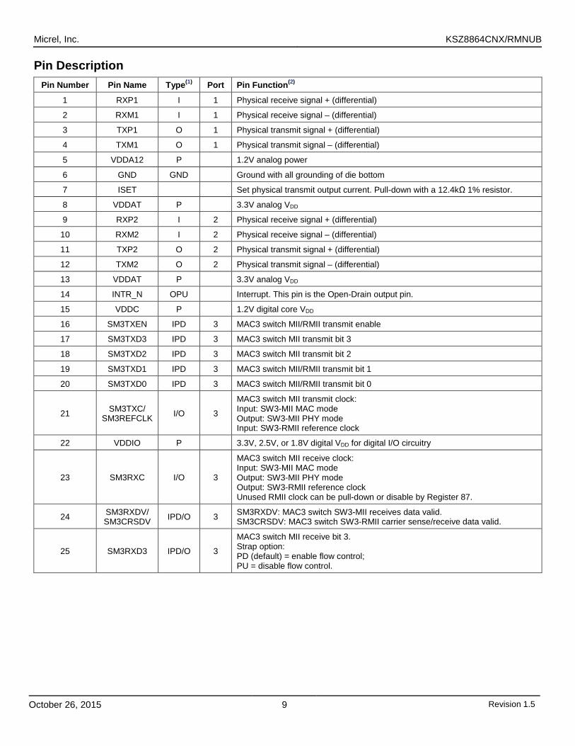
Pin Description Pin Number Pin Name Type(1) Port Pin Function(2)
1 RXP1 I 1 Physical receive signal + (differential)
2 RXM1 I 1 Physical receive signal – (differential)
3 TXP1 O 1 Physical transmit signal + (differential)
4 TXM1 O 1 Physical transmit signal – (differential)
5 VDDA12 P 1.2V analog power
6 GND GND Ground with all grounding of die bottom
7 ISET Set physical transmit output current. Pull-down with a 12.4kΩ 1% resistor.
8 VDDAT P 3.3V analog VDD
9 RXP2 I 2 Physical receive signal + (differential)
10 RXM2 I 2 Physical receive signal – (differential)
11 TXP2 O 2 Physical transmit signal + (differential)
12 TXM2 O 2 Physical transmit signal – (differential)
13 VDDAT P 3.3V analog VDD
14 INTR_N OPU Interrupt. This pin is the Open-Drain output pin.
15 VDDC P 1.2V digital core VDD
16 SM3TXEN IPD 3 MAC3 switch MII/RMII transmit enable
17 SM3TXD3 IPD 3 MAC3 switch MII transmit bit 3
18 SM3TXD2 IPD 3 MAC3 switch MII transmit bit 2
19 SM3TXD1 IPD 3 MAC3 switch MII/RMII transmit bit 1
20 SM3TXD0 IPD 3 MAC3 switch MII/RMII transmit bit 0
21 SM3TXC/ SM3REFCLK I/O 3
MAC3 switch MII transmit clock: Input: SW3-MII MAC mode Output: SW3-MII PHY mode Input: SW3-RMII reference clock
22 VDDIO P 3.3V, 2.5V, or 1.8V digital VDD for digital I/O circuitry
23 SM3RXC I/O 3
MAC3 switch MII receive clock: Input: SW3-MII MAC mode Output: SW3-MII PHY mode Output: SW3-RMII reference clock Unused RMII clock can be pull-down or disable by Register 87.
24 SM3RXDV/ SM3CRSDV IPD/O 3 SM3RXDV: MAC3 switch SW3-MII receives data valid.
SM3CRSDV: MAC3 switch SW3-RMII carrier sense/receive data valid.
25 SM3RXD3 IPD/O 3
MAC3 switch MII receive bit 3. Strap option: PD (default) = enable flow control; PU = disable flow control.
Micrel, Inc. KSZ8864CNX/RMNUB
October 26, 2015 10 Revision 1.5
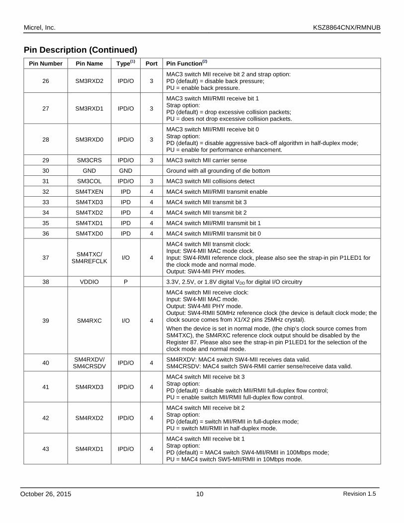
Pin Description (Continued)
Pin Number Pin Name Type(1) Port Pin Function(2)
26 SM3RXD2 IPD/O 3 MAC3 switch MII receive bit 2 and strap option: PD (default) = disable back pressure; PU = enable back pressure.
27 SM3RXD1 IPD/O 3
MAC3 switch MII/RMII receive bit 1 Strap option: PD (default) = drop excessive collision packets; PU = does not drop excessive collision packets.
28 SM3RXD0 IPD/O 3
MAC3 switch MII/RMII receive bit 0 Strap option: PD (default) = disable aggressive back-off algorithm in half-duplex mode; PU = enable for performance enhancement.
29 SM3CRS IPD/O 3 MAC3 switch MII carrier sense
30 GND GND Ground with all grounding of die bottom
31 SM3COL IPD/O 3 MAC3 switch MII collisions detect
32 SM4TXEN IPD 4 MAC4 switch MII/RMII transmit enable
33 SM4TXD3 IPD 4 MAC4 switch MII transmit bit 3
34 SM4TXD2 IPD 4 MAC4 switch MII transmit bit 2
35 SM4TXD1 IPD 4 MAC4 switch MII/RMII transmit bit 1
36 SM4TXD0 IPD 4 MAC4 switch MII/RMII transmit bit 0
37 SM4TXC/ SM4REFCLK I/O 4
MAC4 switch MII transmit clock: Input: SW4-MII MAC mode clock. Input: SW4-RMII reference clock, please also see the strap-in pin P1LED1 for the clock mode and normal mode. Output: SW4-MII PHY modes.
38 VDDIO P 3.3V, 2.5V, or 1.8V digital VDD for digital I/O circuitry
39 SM4RXC I/O 4
MAC4 switch MII receive clock: Input: SW4-MII MAC mode. Output: SW4-MII PHY mode. Output: SW4-RMII 50MHz reference clock (the device is default clock mode; the clock source comes from X1/X2 pins 25MHz crystal). When the device is set in normal mode, (the chip’s clock source comes from SM4TXC), the SM4RXC reference clock output should be disabled by the Register 87. Please also see the strap-in pin P1LED1 for the selection of the clock mode and normal mode.
40 SM4RXDV/ SM4CRSDV IPD/O 4 SM4RXDV: MAC4 switch SW4-MII receives data valid.
SM4CRSDV: MAC4 switch SW4-RMII carrier sense/receive data valid.
41 SM4RXD3 IPD/O 4
MAC4 switch MII receive bit 3 Strap option: PD (default) = disable switch MII/RMII full-duplex flow control; PU = enable switch MII/RMII full-duplex flow control.
42 SM4RXD2 IPD/O 4
MAC4 switch MII receive bit 2 Strap option: PD (default) = switch MII/RMII in full-duplex mode; PU = switch MII/RMII in half-duplex mode.
43 SM4RXD1 IPD/O 4
MAC4 switch MII receive bit 1 Strap option: PD (default) = MAC4 switch SW4-MII/RMII in 100Mbps mode; PU = MAC4 switch SW5-MII/RMII in 10Mbps mode.
Micrel, Inc. KSZ8864CNX/RMNUB
October 26, 2015 11 Revision 1.5
Pin Description (Continued)
Pin Number Pin Name Type(1) Port Pin Function(2)
44 SM4RXD0 IPD/O 4
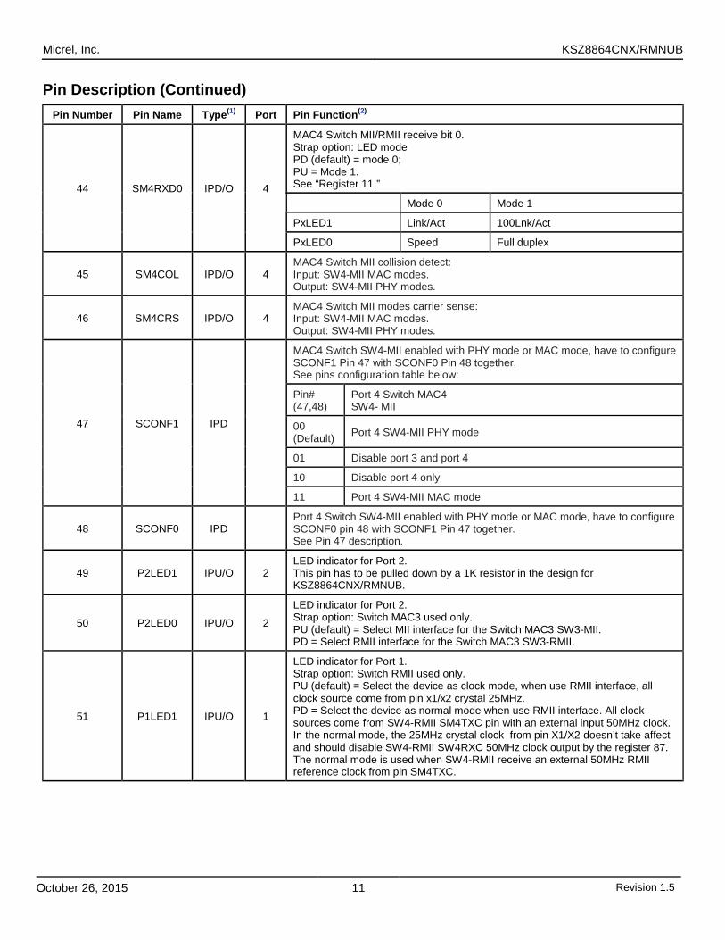
MAC4 Switch MII/RMII receive bit 0. Strap option: LED mode PD (default) = mode 0; PU = Mode 1. See “Register 11.”
Mode 0 Mode 1
PxLED1 Link/Act 100Lnk/Act
PxLED0 Speed Full duplex
45 SM4COL IPD/O 4 MAC4 Switch MII collision detect: Input: SW4-MII MAC modes. Output: SW4-MII PHY modes.
46 SM4CRS IPD/O 4 MAC4 Switch MII modes carrier sense: Input: SW4-MII MAC modes. Output: SW4-MII PHY modes.
47 SCONF1 IPD
MAC4 Switch SW4-MII enabled with PHY mode or MAC mode, have to configure SCONF1 Pin 47 with SCONF0 Pin 48 together. See pins configuration table below:
Pin# (47,48)
Port 4 Switch MAC4 SW4- MII
00 (Default) Port 4 SW4-MII PHY mode
01 Disable port 3 and port 4
10 Disable port 4 only
11 Port 4 SW4-MII MAC mode
48 SCONF0 IPD Port 4 Switch SW4-MII enabled with PHY mode or MAC mode, have to configure SCONF0 pin 48 with SCONF1 Pin 47 together. See Pin 47 description.
49 P2LED1 IPU/O 2 LED indicator for Port 2. This pin has to be pulled down by a 1K resistor in the design for KSZ8864CNX/RMNUB.
50 P2LED0 IPU/O 2
LED indicator for Port 2. Strap option: Switch MAC3 used only. PU (default) = Select MII interface for the Switch MAC3 SW3-MII. PD = Select RMII interface for the Switch MAC3 SW3-RMII.
51 P1LED1 IPU/O 1
LED indicator for Port 1. Strap option: Switch RMII used only. PU (default) = Select the device as clock mode, when use RMII interface, all clock source come from pin x1/x2 crystal 25MHz. PD = Select the device as normal mode when use RMII interface. All clock sources come from SW4-RMII SM4TXC pin with an external input 50MHz clock. In the normal mode, the 25MHz crystal clock from pin X1/X2 doesn’t take affect and should disable SW4-RMII SW4RXC 50MHz clock output by the register 87. The normal mode is used when SW4-RMII receive an external 50MHz RMII reference clock from pin SM4TXC.
Micrel, Inc. KSZ8864CNX/RMNUB
October 26, 2015 12 Revision 1.5
Pin Description (Continued)
Pin Number Pin Name Type(1) Port Pin Function(2)
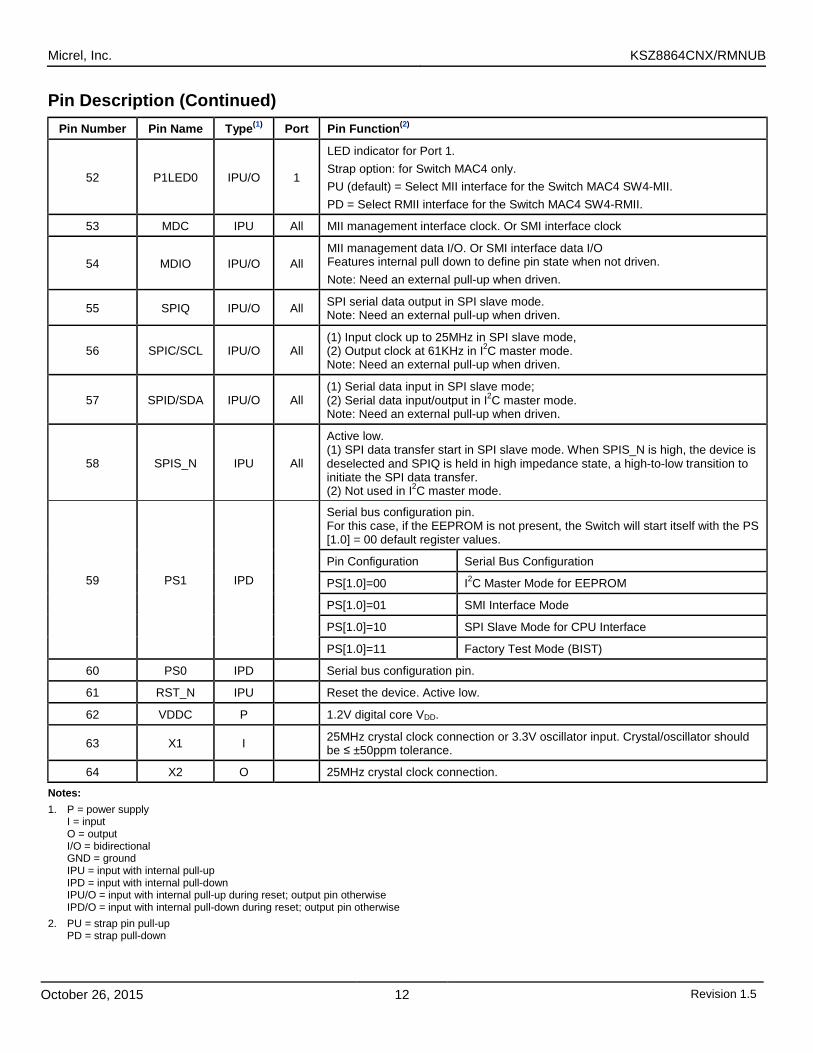
52 P1LED0 IPU/O 1
LED indicator for Port 1. Strap option: for Switch MAC4 only. PU (default) = Select MII interface for the Switch MAC4 SW4-MII. PD = Select RMII interface for the Switch MAC4 SW4-RMII.
53 MDC IPU All MII management interface clock. Or SMI interface clock
54 MDIO IPU/O All MII management data I/O. Or SMI interface data I/O Features internal pull down to define pin state when not driven. Note: Need an external pull-up when driven.
55 SPIQ IPU/O All SPI serial data output in SPI slave mode. Note: Need an external pull-up when driven.
56 SPIC/SCL IPU/O All (1) Input clock up to 25MHz in SPI slave mode, (2) Output clock at 61KHz in I2C master mode. Note: Need an external pull-up when driven.
57 SPID/SDA IPU/O All (1) Serial data input in SPI slave mode; (2) Serial data input/output in I2C master mode. Note: Need an external pull-up when driven.
58 SPIS_N IPU All
Active low. (1) SPI data transfer start in SPI slave mode. When SPIS_N is high, the device is deselected and SPIQ is held in high impedance state, a high-to-low transition to initiate the SPI data transfer. (2) Not used in I2C master mode.
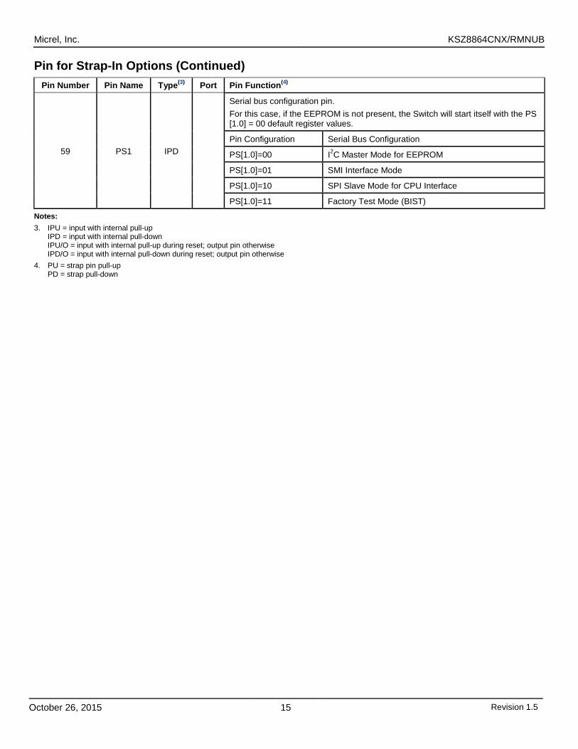
59 PS1 IPD
Serial bus configuration pin. For this case, if the EEPROM is not present, the Switch will start itself with the PS [1.0] = 00 default register values.
Pin Configuration Serial Bus Configuration
PS[1.0]=00 I2C Master Mode for EEPROM
PS[1.0]=01 SMI Interface Mode
PS[1.0]=10 SPI Slave Mode for CPU Interface
PS[1.0]=11 Factory Test Mode (BIST)
60 PS0 IPD Serial bus configuration pin.
61 RST_N IPU Reset the device. Active low.
62 VDDC P 1.2V digital core VDD.
63 X1 I 25MHz crystal clock connection or 3.3V oscillator input. Crystal/oscillator should be ≤ ±50ppm tolerance.
64 X2 O 25MHz crystal clock connection.
Notes: 1. P = power supply
I = input O = output I/O = bidirectional GND = ground IPU = input with internal pull-up IPD = input with internal pull-down IPU/O = input with internal pull-up during reset; output pin otherwise IPD/O = input with internal pull-down during reset; output pin otherwise
2. PU = strap pin pull-up PD = strap pull-down
Micrel, Inc. KSZ8864CNX/RMNUB
October 26, 2015 13 Revision 1.5
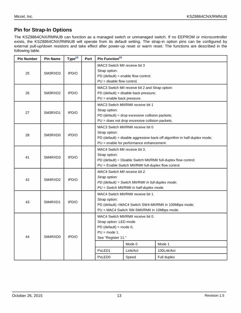
Pin for Strap-In Options The KSZ8864CNX/RMNUB can function as a managed switch or unmanaged switch. If no EEPROM or microcontroller exists, the KSZ8864CNX/RMNUB will operate from its default setting. The strap-in option pins can be configured by external pull-up/down resistors and take effect after power-up reset or warm reset. The functions are described in the following table.
Pin Number Pin Name Type(3) Port Pin Function(4)
25 SM3RXD3 IPD/O
MAC3 Switch MII receive bit 3 Strap option: PD (default) = enable flow control; PU = disable flow control.
26 SM3RXD2 IPD/O MAC3 Switch MII receive bit 2 and Strap option: PD (default) = disable back pressure; PU = enable back pressure.
27 SM3RXD1 IPD/O
MAC3 Switch MII/RMII receive bit 1 Strap option: PD (default) = drop excessive collision packets; PU = does not drop excessive collision packets.
28 SM3RXD0 IPD/O
MAC3 Switch MII/RMII receive bit 0 Strap option: PD (default) = disable aggressive back-off algorithm in half-duplex mode; PU = enable for performance enhancement.
41 SM4RXD3 IPD/O
MAC4 Switch MII receive bit 3. Strap option: PD (default) = Disable Switch MII/RMII full-duplex flow control; PU = Enable Switch MII/RMII full-duplex flow control.
42 SM4RXD2 IPD/O
MAC4 Switch MII receive bit 2. Strap option: PD (default) = Switch MII/RMII in full-duplex mode; PU = Switch MII/RMII in half-duplex mode.
43 SM4RXD1 IPD/O
MAC4 Switch MII/RMII receive bit 1. Strap option: PD (default) =MAC4 Switch SW4-MII/RMII in 100Mbps mode; PU = MAC4 Switch SW-5MII/RMII in 10Mbps mode.
44 SM4RXD0 IPD/O
MAC4 Switch MII/RMII receive bit 0. Strap option: LED mode PD (default) = mode 0; PU = mode 1. See “Register 11.”
Mode 0 Mode 1
PxLED1 Link/Act 100Lnk/Act
PxLED0 Speed Full duplex
Micrel, Inc. KSZ8864CNX/RMNUB
October 26, 2015 14 Revision 1.5
Pin for Strap-In Options (Continued)
Pin Number Pin Name Type(3) Port Pin Function(4)
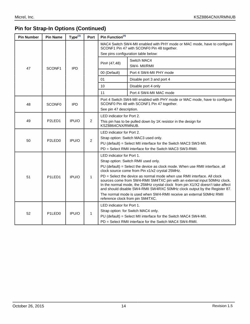
47 SCONF1 IPD
MAC4 Switch SW4-MII enabled with PHY mode or MAC mode, have to configure SCONF1 Pin 47 with SCONF0 Pin 48 together. See pins configuration table below:
Pin# (47,48) Switch MAC4 SW4- MII/RMII
00 (Default) Port 4 SW4-MII PHY mode
01 Disable port 3 and port 4
10 Disable port 4 only
11 Port 4 SW4-MII MAC mode
48 SCONF0 IPD Port 4 Switch SW4-MII enabled with PHY mode or MAC mode, have to configure SCONF0 Pin 48 with SCONF1 Pin 47 together. See pin 47 description.
49 P2LED1 IPU/O 2 LED indicator for Port 2. This pin has to be pulled down by 1K resistor in the design for KSZ8864CNX/RMNUB.
50 P2LED0 IPU/O 2
LED indicator for Port 2. Strap option: Switch MAC3 used only. PU (default) = Select MII interface for the Switch MAC3 SW3-MII. PD = Select RMII interface for the Switch MAC3 SW3-RMII.
51 P1LED1 IPU/O 1
LED indicator for Port 1. Strap option: Switch RMII used only. PU (default) = Select the device as clock mode. When use RMII interface, all clock source come from Pin x1/x2 crystal 25MHz. PD = Select the device as normal mode when use RMII interface. All clock sources come from SW4-RMII SM4TXC pin with an external input 50MHz clock. In the normal mode, the 25MHz crystal clock from pin X1/X2 doesn’t take affect and should disable SW4-RMII SW4RXC 50MHz clock output by the Register 87. The normal mode is used when SW4-RMII receive an external 50MHz RMII reference clock from pin SM4TXC.
52 P1LED0 IPU/O 1
LED indicator for Port 1. Strap option: for Switch MAC4 only. PU (default) = Select MII interface for the Switch MAC4 SW4-MII. PD = Select RMII interface for the Switch MAC4 SW4-RMII.
Micrel, Inc. KSZ8864CNX/RMNUB
October 26, 2015 15 Revision 1.5
Pin for Strap-In Options (Continued) Pin Number Pin Name Type(3) Port Pin Function(4)
59 PS1 IPD
Serial bus configuration pin. For this case, if the EEPROM is not present, the Switch will start itself with the PS [1.0] = 00 default register values.
Pin Configuration Serial Bus Configuration
PS[1.0]=00 I2C Master Mode for EEPROM
PS[1.0]=01 SMI Interface Mode
PS[1.0]=10 SPI Slave Mode for CPU Interface
PS[1.0]=11 Factory Test Mode (BIST)
Notes: 3. IPU = input with internal pull-up
IPD = input with internal pull-down IPU/O = input with internal pull-up during reset; output pin otherwise IPD/O = input with internal pull-down during reset; output pin otherwise
4. PU = strap pin pull-up PD = strap pull-down
Micrel, Inc. KSZ8864CNX/RMNUB
October 26, 2015 16 Revision 1.5
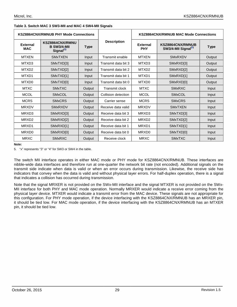
Introduction The KSZ8864CNX/RMNUB contains two 10/100 physical layer transceivers and four media access control (MAC) units with an integrated Layer 2 managed switch. The device runs in multiple modes. They are two copper plus two MAC MII, two copper plus two MAC RMII, two copper plus 1 MAC MII plus 1 MAC RMII, and two copper plus 1 MAC MII or 1 MAC RMII. These are useful for implementing multiple products in many applications.
The KSZ8864CNX/RMNUB has the flexibility to reside in a managed or unmanaged design. In a managed design, a host processor has complete control of the KSZ8864CNX/RMNUB via the SPI bus, or partial control via the MDC/MDIO interface. An unmanaged design is achieved through I/O strapping or EEPROM programming at system reset time.
On the media side, the KSZ8864CNX/RMNUB supports IEEE 802.3 10BASE-T/100BASE-TX on all ports with Auto MDI/MDIX. The KSZ8864CNX/RMNUB can be used as fully managed 4-port switch through two microprocessors by its two MII interface or RMII interface for an advance management application.
Physical signal transmission and reception are enhanced through the use of patented analog circuitry with enhanced mixed signal technology that makes the design more efficient and allows for lower power consumption and smaller chip die size.
Major enhancements from the KS8864RMN to the KSZ8864CNX/RMNUB include further power saving, adding Micrel’s LinkMD® feature and 0.11um silicon process technology. The KSZ8864CNX/RMNUB is completely pin-compatible with the KSZ8864RMN.
Functional Overview: Physical Layer Transceiver 100BASE-TX Transmit The 100BASE-TX transmit function performs parallel-to-serial conversions, 4B/5B coding, scrambling, NRZ-to-NRZI conversions, MLT3 encoding, and transmission. The circuit starts with a parallel-to-serial conversion, which converts the MII data from the MAC into a 125MHz serial bit stream. The data and control stream is then converted into 4B/5B coding, followed by a scrambler. The serialized data is further converted from NRZ to NRZI format, and then transmitted in MLT3 current output. The output current is set by an external 1% 12.4kΩ resistor for the 1:1 transformer ratio. It has a typical rise/fall time of 4ns and complies with the ANSI TP-PMD standard regarding amplitude balance, overshoot, and timing jitter. The wave-shaped 10BASE-T output is also incorporated into the 100BASE-TX transmitter.
100BASE-TX Receive The 100BASE-TX receiver function performs adaptive equalization, DC restoration, MLT3-to-NRZI conversion, data and clock recovery, NRZI-to-NRZ conversion, de-scrambling, 4B/5B decoding, and serial-to-parallel conversion. The receiving side starts with the equalization filter to compensate for inter-symbol interference (ISI) over the twisted pair cable. Because the amplitude loss and phase distortion is a function of the length of the cable, the equalizer has to adjust its characteristics to optimize the performance. In this design, the variable equalizer will make an initial estimation based on comparisons of incoming signal strength against some known cable characteristics, then tunes itself for optimization. This is an ongoing process and it can self-adjust against environmental changes such as temperature variations.
The equalized signal then goes through a DC restoration and data conversion block. The DC restoration circuit is used to compensate for the effect of baseline wander and improve the dynamic range. The differential data conversion circuit converts the MLT3 format back to NRZI. The slicing threshold is also adaptive.
The clock recovery circuit extracts the 125MHz clock from the edges of the NRZI signal. This recovered clock is then used to convert the NRZI signal into the NRZ format. The signal is then sent through the de-scrambler, followed by the 4B/5B decoder. Finally, the NRZ serial data is converted to the MII format and provided as the input data to the MAC.
PLL Clock Synthesizer The KSZ8864CNX/RMNUB generates 125MHz, 83MHz, 41MHz, 25MHz, and 10MHz clocks for system timing. Internal clocks are generated from an external 25MHz crystal or oscillator.
Scrambler/De-Scrambler (100BASE-TX only) The purpose of the scrambler is to spread the power spectrum of the signal in order to reduce EMI and baseline wander. The data is scrambled through the use of an 11-bit wide linear feedback shift register (LFSR). This can generate a 2047-bit non-repetitive sequence. The receiver will then de-scramble the incoming data stream with the same sequence at the transmitter.
Micrel, Inc. KSZ8864CNX/RMNUB
October 26, 2015 17 Revision 1.5
10BASE-T Transmit The output 10BASE-T driver is incorporated into the 100BASE-T driver to allow transmission with the same magnetics. They are internally wave-shaped and pre-emphasized into outputs with typical 2.3V amplitude. The harmonic contents are at least 27dB below the fundamental when driven by an all-ones Manchester-encoded signal.
10BASE-T Receive On the receive side, input buffer and level detecting squelch circuits are employed. A differential input receiver circuit and a PLL perform the decoding function. The Manchester-encoded data stream is separated into clock signal and NRZ data. A squelch circuit rejects signals with levels less than 400mV or with short pulse widths in order to prevent noises at the RXP or RXM input from falsely triggering the decoder. When the input exceeds the squelch limit, the PLL locks onto the incoming signal and the KSZ8864CNX/RMNUB decodes a data frame. The receiver clock is maintained active during idle periods in between data reception.
MDI/MDI-X Auto Crossover To eliminate the need for crossover cables between similar devices, the KSZ8864CNX/RMNUB supports HP Auto MDI/MDI-X and IEEE 802.3u standard MDI/MDI-X auto crossover. HP Auto MDI/MDI-X is the default.
The auto-sense function detects remote transmit and receive pairs and correctly assigns transmit and receive pairs for the switch device. This feature is extremely useful when end users are unaware of cable types and saves on an additional uplink configuration connection. The auto-crossover feature can be disabled through the port control registers or MIIM PHY registers. The IEEE 802.3u standard MDI and MDI-X definitions are: Table 1. MDI/MDI-X Pin Definitions
MDI MDI-X
RJ-45 Pins Signals RJ-45 Pins Signals
1 TD+ 1 RD+
2 TD- 2 RD-
3 RD+ 3 TD+
6 RD- 6 TD-
Micrel, Inc. KSZ8864CNX/RMNUB
October 26, 2015 18 Revision 1.5
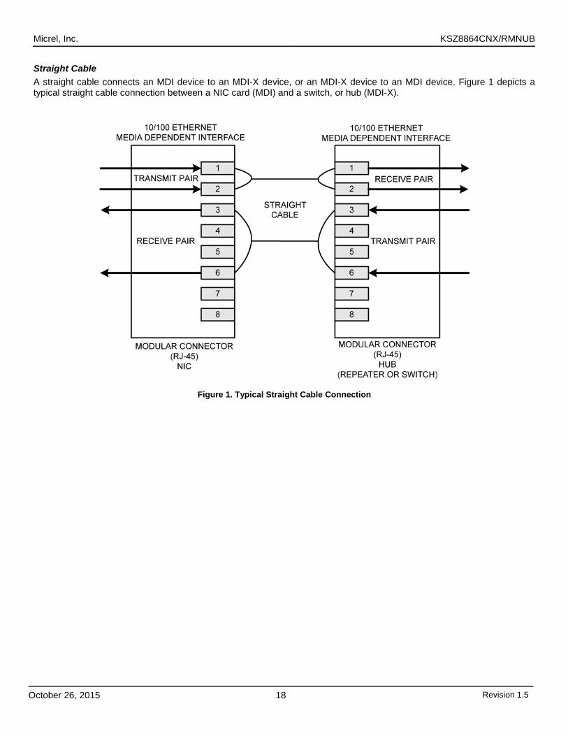
Straight Cable A straight cable connects an MDI device to an MDI-X device, or an MDI-X device to an MDI device. Figure 1 depicts a typical straight cable connection between a NIC card (MDI) and a switch, or hub (MDI-X).
Figure 1. Typical Straight Cable Connection
Micrel, Inc. KSZ8864CNX/RMNUB
October 26, 2015 19 Revision 1.5
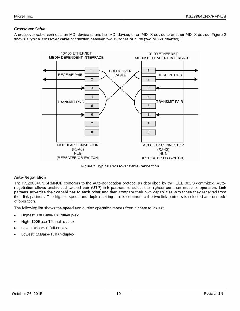
Crossover Cable A crossover cable connects an MDI device to another MDI device, or an MDI-X device to another MDI-X device. Figure 2 shows a typical crossover cable connection between two switches or hubs (two MDI-X devices).
Figure 2. Typical Crossover Cable Connection
Auto-Negotiation The KSZ8864CNX/RMNUB conforms to the auto-negotiation protocol as described by the IEEE 802.3 committee. Auto-negotiation allows unshielded twisted pair (UTP) link partners to select the highest common mode of operation. Link partners advertise their capabilities to each other and then compare their own capabilities with those they received from their link partners. The highest speed and duplex setting that is common to the two link partners is selected as the mode of operation.
The following list shows the speed and duplex operation modes from highest to lowest.
• Highest: 100Base-TX, full-duplex • High: 100Base-TX, half-duplex • Low: 10Base-T, full-duplex • Lowest: 10Base-T, half-duplex
Micrel, Inc. KSZ8864CNX/RMNUB
October 26, 2015 20 Revision 1.5
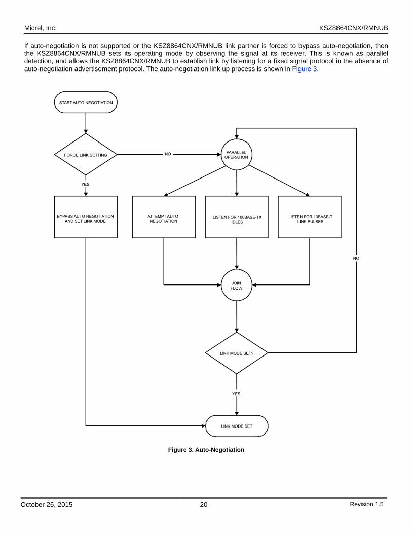
If auto-negotiation is not supported or the KSZ8864CNX/RMNUB link partner is forced to bypass auto-negotiation, then the KSZ8864CNX/RMNUB sets its operating mode by observing the signal at its receiver. This is known as parallel detection, and allows the KSZ8864CNX/RMNUB to establish link by listening for a fixed signal protocol in the absence of auto-negotiation advertisement protocol. The auto-negotiation link up process is shown in Figure 3.
Figure 3. Auto-Negotiation
Micrel, Inc. KSZ8864CNX/RMNUB
October 26, 2015 21 Revision 1.5
LinkMD® Cable Diagnostics The LinkMD® feature utilizes time domain reflectometry (TDR) to analyze the cabling plant for common cabling problems such as open circuits, short circuits, and impedance mismatches.
LinkMD works by sending a pulse of known amplitude and duration down the MDI and MDI-X pairs and then analyzes the shape of the reflected signal. Timing the pulse duration gives an indication of the distance to the cabling fault with maximum distance of 200m and accuracy of ±2m. Internal circuitry displays the TDR information in a user-readable digital format.
Note: Cable diagnostics are only valid for copper connections and do not support fiber optic operation.
Access LinkMD is initiated by accessing the PHY special control/status Registers 42, 58 and the LinkMD result Registers 43, 59 for ports 1 and 2 respectively; and in conjunction with the registers port control 12 and 13 for ports 1 and 2 respectively to disable auto-negotiation and Auto MDI/MDIX.
Alternatively, the MIIM PHY Registers 0 and 1d can also be used for LinkMD access.
Usage The following is a sample procedure for using LinkMD with Registers 42, 43, 44, 45 on port 1.
1. Disable Auto-Negotiation by writing a ‘1’ to Register 44 (0x2c), bit [7]. 2. Disable auto MDI/MDI-X by writing a ‘1’ to Register 45 (0x2d), bit [2] to enable manual control over the differential pair
used to transmit the LinkMD pulse. 3. A software sequence set up to the internal registers for LinkMD only, see an example below. 4. Start cable diagnostic test by writing a ‘1’ to Register 42 (0x2a), bit [4]. This enable bit is self-clearing. 5. Wait (poll) for Register 42 (0x2a), bit [4] to return a ‘0’, and indicating cable diagnostic test is completed. 6. Read cable diagnostic test results in Register 42 (0x2a), bits [6:5]. The results are as follows: 00 = normal condition (valid test)
01 = open condition detected in cable (valid test)
10 = short condition detected in cable (valid test)
11 = cable diagnostic test failed (invalid test)
The ‘11’ case, invalid test, occurs when the KSZ8864 is unable to shut down the link partner. In this instance, the test is not run, since it would be impossible for the KSZ8864 to determine if the detected signal is a reflection of the signal generated or a signal from another source.
7. Get distance to fault by concatenating Register 42 (0x2a), bit [0] and Register 43 (0x2b), bits [7:0]; and multiplying the result by a constant of 0.4. The distance to the cable fault can be determined by the following formula:
D (distance to cable fault) = 0.4 x (Register 42, bit [0], Register 43, bits [7:0])
D (distance to cable fault) is expressed in meters.
Concatenated value of Registers 42 bit [0] and 43 bit [7:0] should be converted to decimal before decrease 26 and multiplying by 0.4.
The constant (0.4) may be calibrated for different cabling conditions, including cables with a velocity of propagation that varies significantly from the norm.
For port 2 and for the MIIM PHY registers, LinkMD usage is similar.
Micrel, Inc. KSZ8864CNX/RMNUB
October 26, 2015 22 Revision 1.5
A LinkMD Example The following is a sample procedure for using LinkMD on port 1.
//Set Force 100/Full and Force MDI-X mode
//W is WRITE the register. R is READ register
W 2c ff
W 2d 04
//Set Internal Registers Temporary Adjustment for LinkMD
W 47 b0
W 27 00
W 37 04 (value=04 for port1, value=05 for port2)
W 47 40 (bit6=1 for port1, bit5=1 for port2)
W 27 00
W 37 00
//Enable LinkMD Testing with Fault Cable for port 1
W 2a 10
R 2a
R 2b
//Result analysis based on the values of the Register 0x2a and 0x2b for port 1:
//The Register 0x2a bits [6-5] are for the open or the short detection.
//The Register 0x2a bit [0] + the Register 0x2b bits [7-0] = Vct_Fault [8-0]
//The distance to fault is about 0.4 x Vct_Fault [8-0] – 26
Note: After end the testing, set all registers above to their default values. The default values are ‘00’ for the Register (0x37) and the Register (0x47)
On-Chip Termination Resistors The KSZ8864CNX/RMNUB reduces the board cost and simplifies the board layout by using on-chip termination resistors for all ports and RX/TX differential pairs without the external termination resistors. The combination of the on-chip termination and internal biasing will save the power consumption as compared to using external biasing and termination resistors, and the transformer will not consume power any more. The center tap of the transformer does not need to be tied to the analog power due to have this feature of the internal biasing.
Micrel, Inc. KSZ8864CNX/RMNUB
October 26, 2015 23 Revision 1.5
Functional Overview: Power Management The KSZ8864CNX/RMNUB can also use multiple power levels of 3.3V, 2.5V, or 1.8V for VDDIO to support different I/O voltages.
The KSZ8864CNX/RMNUB supports an enhanced power management feature in the low power state with energy detection to ensure low power dissipation during device idle periods. There are five operation modes under the power management function, which is controlled by the Register 14 bit [4:3] and the Register Port Control 6 bit3 as shown below:
Register 14 bit [4:3] = 00 Normal Operation Mode
Register 14 bit [4:3] = 01 Energy Detect Mode
Register 14 bit [4:3] = 10 Soft Power Down Mode
Register 14 bit [4:3] = 11 Power Saving Mode
The Register Port Control 6 bit 3 =1 is for the Port-Based Power-Down Mode
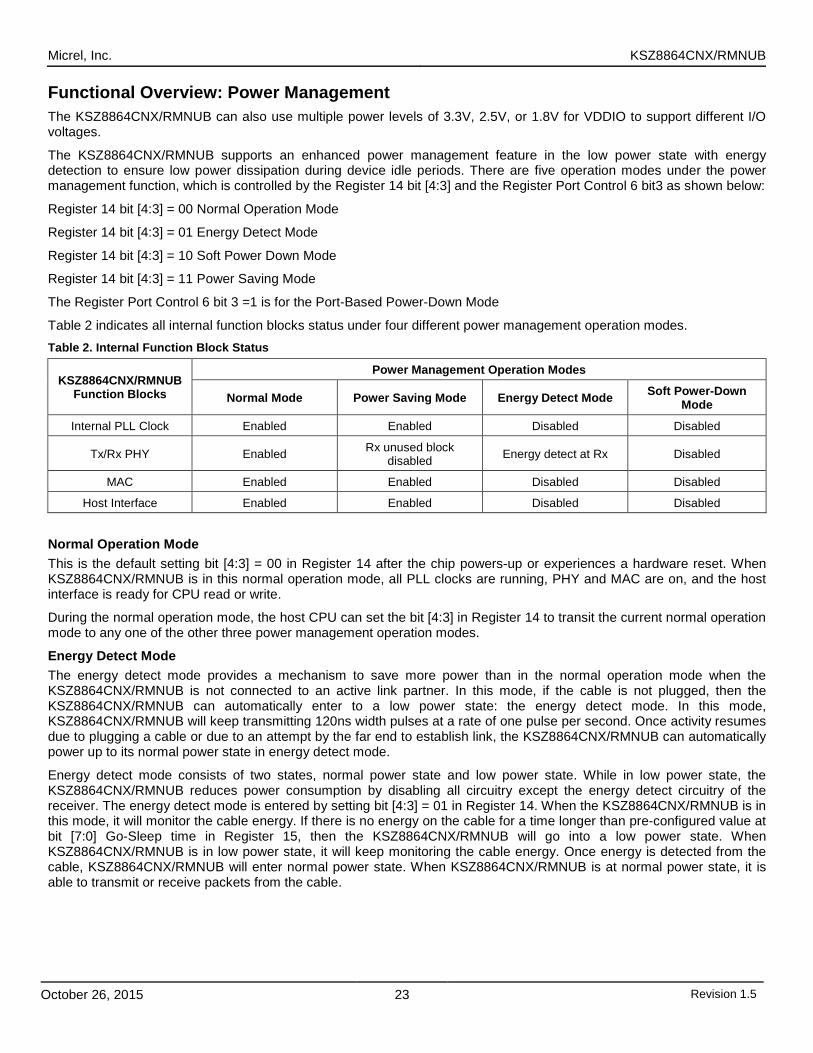
Table 2 indicates all internal function blocks status under four different power management operation modes. Table 2. Internal Function Block Status
KSZ8864CNX/RMNUB Function Blocks
Power Management Operation Modes
Normal Mode Power Saving Mode Energy Detect Mode Soft Power-Down Mode
Internal PLL Clock Enabled Enabled Disabled Disabled
Tx/Rx PHY Enabled Rx unused block disabled Energy detect at Rx Disabled
MAC Enabled Enabled Disabled Disabled
Host Interface Enabled Enabled Disabled Disabled
Normal Operation Mode This is the default setting bit [4:3] = 00 in Register 14 after the chip powers-up or experiences a hardware reset. When KSZ8864CNX/RMNUB is in this normal operation mode, all PLL clocks are running, PHY and MAC are on, and the host interface is ready for CPU read or write.
During the normal operation mode, the host CPU can set the bit [4:3] in Register 14 to transit the current normal operation mode to any one of the other three power management operation modes.
Energy Detect Mode The energy detect mode provides a mechanism to save more power than in the normal operation mode when the KSZ8864CNX/RMNUB is not connected to an active link partner. In this mode, if the cable is not plugged, then the KSZ8864CNX/RMNUB can automatically enter to a low power state: the energy detect mode. In this mode, KSZ8864CNX/RMNUB will keep transmitting 120ns width pulses at a rate of one pulse per second. Once activity resumes due to plugging a cable or due to an attempt by the far end to establish link, the KSZ8864CNX/RMNUB can automatically power up to its normal power state in energy detect mode.
Energy detect mode consists of two states, normal power state and low power state. While in low power state, the KSZ8864CNX/RMNUB reduces power consumption by disabling all circuitry except the energy detect circuitry of the receiver. The energy detect mode is entered by setting bit [4:3] = 01 in Register 14. When the KSZ8864CNX/RMNUB is in this mode, it will monitor the cable energy. If there is no energy on the cable for a time longer than pre-configured value at bit [7:0] Go-Sleep time in Register 15, then the KSZ8864CNX/RMNUB will go into a low power state. When KSZ8864CNX/RMNUB is in low power state, it will keep monitoring the cable energy. Once energy is detected from the cable, KSZ8864CNX/RMNUB will enter normal power state. When KSZ8864CNX/RMNUB is at normal power state, it is able to transmit or receive packets from the cable.

Micrel, Inc. KSZ8864CNX/RMNUB
October 26, 2015 24 Revision 1.5
Soft Power-Down Mode The soft power-down mode is entered by setting bit [4:3] = 10 in Register 14. When KSZ8864CNX/RMNUB is in this mode, all PLL clocks are disabled, also all of the PHYs and the MACs are off. Any dummy host access will wake-up this device from its current soft power-down mode to normal operation mode and internal reset will be issued to make all internal registers go to the default values.
Power Saving Mode The power saving mode is entered when auto-negotiation mode is enabled, the cable is disconnected, and by setting bit [4:3] =11 in Register 14. When KSZ8864CNX/RMNUB is in this mode, all PLL clocks are enabled, MAC is on, all internal register values will not change, and the host interface is ready for CPU read or write. This mode mainly controls the PHY transceiver on or off based on the line status to achieve power saving. The PHY remains transmitting and only turns off the unused receiver block. Once activity resumes due to plugging a cable or an attempt by the far end to establish a link, the KSZ8864CNX/RMNUB can automatically enable the PHY to power up to its normal power state from power saving mode.
During this power saving mode, the host CPU can set bit [4:3] in Register 14 to transit the current power saving mode to any one of the other three power management operation modes.
Port-Based Power-Down Mode In addition, the KSZ8864CNX/RMNUB features a per-port power-down mode. To save power, a PHY port that is not in use can be powered down by the Registers Port Control 13 bit3, or MIIM PHY Registers 0 bit11.
Functional Overview: Switch Core Address Look-Up The internal look-up table stores MAC addresses and their associated information. It contains a 1K unicast address table plus switching information. The KSZ8864CNX/RMNUB is guaranteed to learn 1K addresses and distinguishes itself from a hash-based look-up table that, depending upon the operating environment and probabilities, may not guarantee the absolute number of addresses it can learn.
Learning The internal look-up engine updates its table with a new entry if the following conditions are met:
• The received packet’s source address (SA) does not exist in the look-up table. • The received packet is good; the packet has no receiving errors and is of legal length. The look-up engine inserts the qualified SA into the table, along with the port number and time stamp. If the table is full, the last entry of the table is deleted first to make room for the new entry.
Migration The internal look-up engine also monitors whether a station is moved. If this occurs, it updates the table accordingly. Migration happens when the following conditions are met:
• The received packet’s SA is in the table but the associated source port information is different. • The received packet is good; the packet has no receiving errors and is of legal length. The look-up engine will update the existing record in the table with the new source port information.
Aging The look-up engine will update the time stamp information of a record whenever the corresponding SA appears. The time stamp is used in the aging process. If a record is not updated for a period of time, the look-up engine will remove the record from the table. The look-up engine constantly performs the aging process and will continuously remove aging records. The aging period is 300 ±75 seconds. This feature can be enabled or disabled through Register 3. See “Register 3” section for more information.
Micrel, Inc. KSZ8864CNX/RMNUB
October 26, 2015 25 Revision 1.5
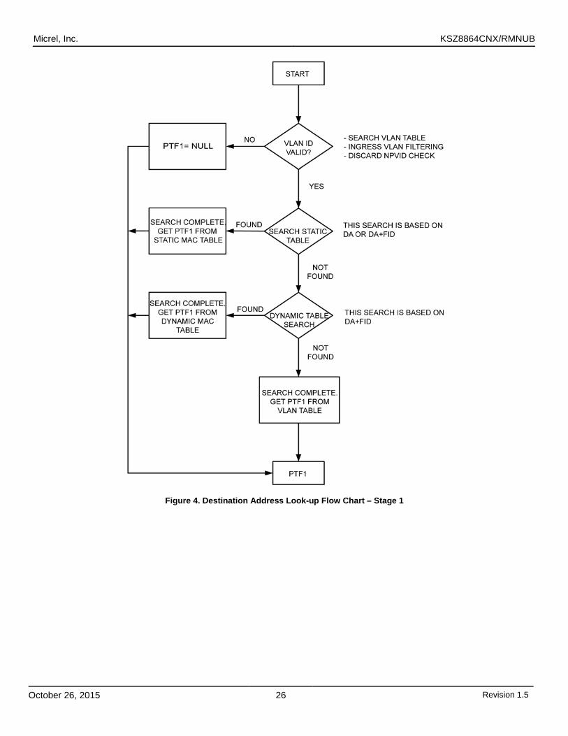
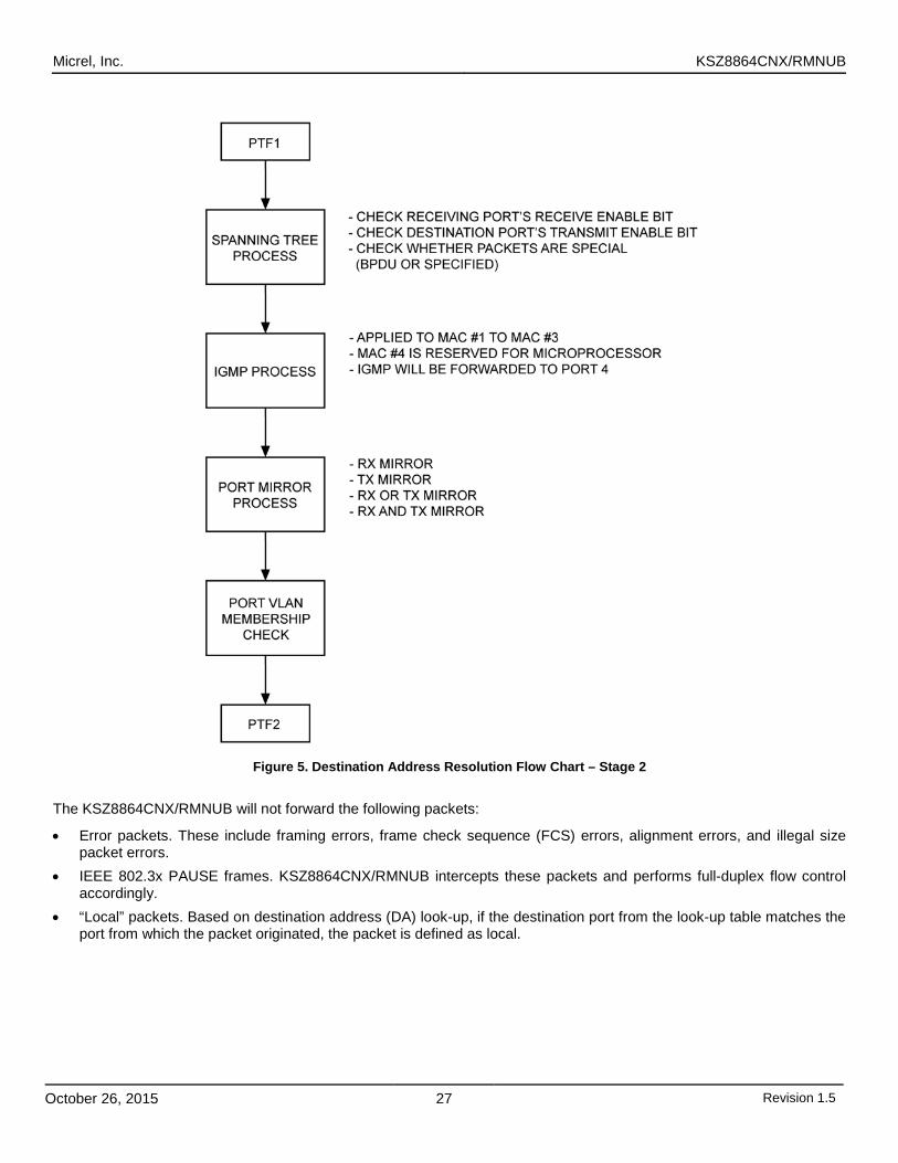
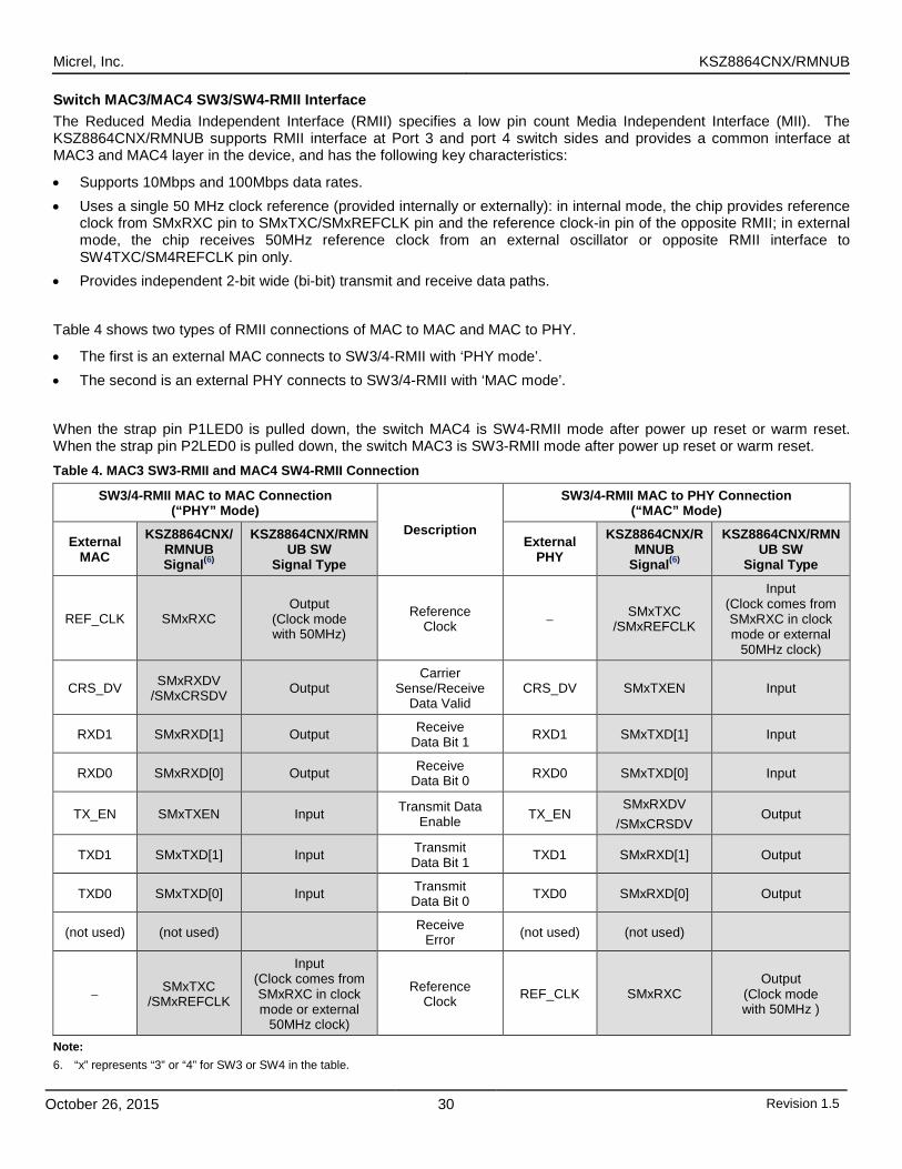
Forwarding The KSZ8864CNX/RMNUB will forward packets using an algorithm that is depicted in the following flowcharts. Figure 6 shows stage one of the forwarding algorithm where the search engine looks up the VLAN ID, static table, and dynamic table for the destination address, and comes up with “port to forward 1” (PTF1). PTF1 is then further modified by the spanning tree, IGMP snooping, port mirroring, and port VLAN processes to come up with “port to forward 2” (PTF2), as shown in Figure 7. This is where the packet will be sent.
KSZ8864CNX/RMNUB will not forward the following packets:
• Error packets. These include framing errors, FCS errors, alignment errors, and illegal size packet errors. • 802.3x pause frames. The KSZ8864CNX/RMNUB will intercept these packets and perform the appropriate actions. • “Local” packets. Based on destination address (DA) look-up. If the destination port from the look-up table matches the
port where the packet was from, the packet is defined as “local.”
Switching Engine The KSZ8864CNX/RMNUB features a high-performance switching engine to move data to and from the MACs, packet buffers. It operates in store and forward mode, while the efficient switching mechanism reduces overall latency. The KSZ8864CNX/RMNUB has a 64KB internal frame buffer. This resource is shared between all five ports. There are a total of 512 buffers available. Each buffer is sized at 128B.
Media Access Controller (MAC) Operation The KSZ8864CNX/RMNUB strictly abides by IEEE 802.3 standards to maximize compatibility.
Inter-Packet Gap (IPG) If a frame is successfully transmitted, the 96-bit time IPG is measured between the two consecutive MTXEN. If the current packet is experiencing collision, the 96-bit time IPG is measured from MCRS and the next MTXEN.
Back-Off Algorithm The KSZ8864CNX/RMNUB implements the IEEE 802.3 binary exponential back-off algorithm and optional “aggressive mode” back-off. After 16 collisions, the packet will be optionally dropped depending on the chip configuration in Register 3. See “Register 3” for additional information.
Late Collision If a transmit packet experiences collisions after 512-bit times of the transmission, the packet will be dropped.
Illegal Frames The KSZ8864CNX/RMNUB discards frames less than 64 bytes and can be programmed to accept frames up to 1536 bytes in Register 4. For special applications, the KSZ8864CNX/RMNUB can also be programmed to accept frames up to 1916 bytes in Register 4. Because the KSZ8864CNX/RMNUB supports VLAN tags, the maximum sizing is adjusted when these tags are present.
Flow Control The KSZ8864CNX/RMNUB supports IEEE 802.3x flow control frames on both transmit and receive sides.
On the receive side, if the KSZ8864CNX/RMNUB receives a pause control frame, the KSZ8864CNX/RMNUB will not transmit the next normal frame until the timer, specified in the pause control frame, expires. If another pause frame is received before the current timer expires, the timer will be updated with the new value in the second pause frame. During this period (being flow controlled), only flow control packets from the KSZ8864CNX/RMNUB will be transmitted.
On the transmit side, the KSZ8864CNX/RMNUB has intelligent and efficient ways to determine when to invoke flow control. The flow control is based on the availability of system resources, including available buffers, available transmit queues, and available receive queues.
The KSZ8864CNX/RMNUB flow controls a port that has just received a packet if the destination port resource is busy. The KSZ8864CNX/RMNUB issues a flow control frame (XOFF), containing the maximum pause time defined in IEEE 802.3x. Once the resource is freed up, the KSZ8864CNX/RMNUB sends out the other flow control frame (XON) with zero pause time to turn off the flow control (turn on transmission to the port). A hysteresis feature is also provided to prevent over-activation and deactivation of the flow control mechanism.
The KSZ8864CNX/RMNUB flow controls all ports if the receive queue becomes full.
Micrel, Inc. KSZ8864CNX/RMNUB
October 26, 2015 26 Revision 1.5
Figure 4. Destination Address Look-up Flow Chart – Stage 1
Micrel, Inc. KSZ8864CNX/RMNUB
October 26, 2015 27 Revision 1.5
Figure 5. Destination Address Resolution Flow Chart – Stage 2
The KSZ8864CNX/RMNUB will not forward the following packets:
• Error packets. These include framing errors, frame check sequence (FCS) errors, alignment errors, and illegal size packet errors.
• IEEE 802.3x PAUSE frames. KSZ8864CNX/RMNUB intercepts these packets and performs full-duplex flow control accordingly.
• “Local” packets. Based on destination address (DA) look-up, if the destination port from the look-up table matches the port from which the packet originated, the packet is defined as local.
Micrel, Inc. KSZ8864CNX/RMNUB
October 26, 2015 28 Revision 1.5
Half-Duplex Back Pressure The KSZ8864CNX/RMNUB also provides a half-duplex back pressure option (note: this is not listed in IEEE 802.3 standards). The activation and deactivation conditions are the same as the ones given for full-duplex mode. If back pressure is required, the KSZ8864CNX/RMNUB sends preambles to defer the other station's transmission (carrier sense deference). To avoid jabber and excessive deference as defined in IEEE 802.3 standard, after a certain period of time, the KSZ8864CNX/RMNUB discontinues carrier sense but raises it quickly after it drops packets to inhibit other transmissions. This short silent time (no carrier sense) is to prevent other stations from sending out packets and keeps other stations in a carrier sense deferred state. If the port has packets to send during a back pressure situation, the carrier-sense-type back pressure is interrupted and those packets are transmitted instead. If there are no more packets to send, carrier-sense-type back pressure becomes active again until switch resources are free. If a collision occurs, the binary exponential backoff algorithm is skipped and carrier sense is generated immediately, reducing the chance of further colliding and maintaining carrier sense to prevent reception of packets. To ensure no packet loss in 10BASE-T or 100BASE-TX half-duplex modes, the user must enable the following:
• Aggressive backoff (Register 3, bit 0) • No excessive collision drop (Register 4, bit 3) • Back pressure (Register 4, bit 5)
These bits are not set as the default because they are not the IEEE standard.
Broadcast Storm Protection The KSZ8864CNX/RMNUB has an intelligent option to protect the switch system from receiving too many broadcast packets. Broadcast packets are normally forwarded to all ports except the source port and thus use too many switch resources (bandwidth and available space in transmit queues). The KSZ8864CNX/RMNUB has the option to include “multicast packets” for storm control. The broadcast storm rate parameters are programmed globally and can be enabled or disabled on a per port basis. The rate is based on a 50ms (0.05s) interval for 100BT and a 500ms (0.5s) interval for 10BT. At the beginning of each interval, the counter is cleared to zero and the rate limit mechanism starts to count the number of bytes during the interval. The rate definition is described in Global Registers 6 and 7. The default setting for Global Registers 6 and 7 is 0x4A (74 decimal). This is equal to a rate of 1%, calculated as follows:
148,800 frames/sec × 50ms (0.05s)/interval × 1% = 74 frames/interval (approx.) = 0x4A.
MII Interface Operation The media independent interface (MII) is specified by the IEEE 802.3 committee and provides a common interface between physical layer and MAC layer devices. The KSZ8864CNX/RMNUB provides two MAC layer interfaces for MAC 3 and MAC 4. Each of these MII/RMII interfaces contains two distinct groups of signals, one for transmission and the other for receiving.
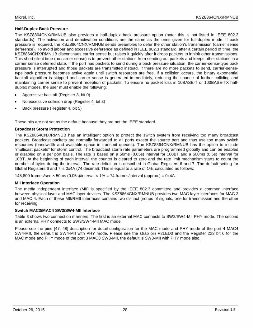
Switch MAC3/MAC4 SW3/SW4-MII Interface Table 3 shows two connection manners. The first is an external MAC connects to SW3/SW4-MII PHY mode. The second is an external PHY connects to SW3/SW4-MII MAC mode.
Please see the pins [47, 48] description for detail configuration for the MAC mode and PHY mode of the port 4 MAC4 SW4-MII, the default is SW4-MII with PHY mode. Please see the strap pin P2LED0 and the Register 223 bit 6 for the MAC mode and PHY mode of the port 3 MAC3 SW3-MII, the default is SW3-MII with PHY mode also.
Micrel, Inc. KSZ8864CNX/RMNUB
October 26, 2015 29 Revision 1.5
Table 3. Switch MAC 3 SW3-MII and MAC 4 SW4-MII Signals
KSZ8864CNX/RMNUB PHY Mode Connections
Description
KSZ8864CNX/RMNUB MAC Mode Connections
External MAC
KSZ8864CNX/RMNUB SW3/4-MII
Signal(5) Type External
PHY KSZ8864CNX/RMNUB
SW3/4-MII Signal(5) Type
MTXEN SMxTXEN Input Transmit enable MTXEN SMxRXDV Output
MTXD3 SMxTXD[3] Input Transmit data bit 3 MTXD3 SMxRXD[3] Output
MTXD2 SMxTXD[2] Input Transmit data bit 2 MTXD2 SMxRXD[2] Output
MTXD1 SMxTXD[1] Input Transmit data bit 1 MTXD1 SMxRXD[1] Output
MTXD0 SMxTXD[0] Input Transmit data bit 0 MTXD0 SMxRXD[0] Output
MTXC SMxTXC Output Transmit clock MTXC SMxRXC Input
MCOL SMxCOL Output Collision detection MCOL SMxCOL Input
MCRS SMxCRS Output Carrier sense MCRS SMxCRS Input
MRXDV SMxRXDV Output Receive data valid MRXDV SMxTXEN Input
MRXD3 SMxRXD[3] Output Receive data bit 3 MRXD3 SMxTXD[3] Input
MRXD2 SMxRXD[2] Output Receive data bit 2 MRXD2 SMxTXD[2] Input
MRXD1 SMxRXD[1] Output Receive data bit 1 MRXD1 SMxTXD[1] Input
MRXD0 SMxRXD[0] Output Receive data bit 0 MRXD0 SMxTXD[0] Input
MRXC SMxRXC Output Receive clock MRXC SMxTXC Input Note: 5. “x” represents “3” or “4” for SW3 or SW4 in the table.
The switch MII interface operates in either MAC mode or PHY mode for KSZ8864CNX/RMNUB. These interfaces are nibble-wide data interfaces and therefore run at one-quarter the network bit rate (not encoded). Additional signals on the transmit side indicate when data is valid or when an error occurs during transmission. Likewise, the receive side has indicators that convey when the data is valid and without physical layer errors. For half-duplex operation, there is a signal that indicates a collision has occurred during transmission.
Note that the signal MRXER is not provided on the SWx-MII interface and the signal MTXER is not provided on the SWx-MII interface for both PHY and MAC mode operation. Normally MRXER would indicate a receive error coming from the physical layer device. MTXER would indicate a transmit error from the MAC device. These signals are not appropriate for this configuration. For PHY mode operation, if the device interfacing with the KSZ8864CNX/RMNUB has an MRXER pin, it should be tied low. For MAC mode operation, if the device interfacing with the KSZ8864CNX/RMNUB has an MTXER pin, it should be tied low.
Micrel, Inc. KSZ8864CNX/RMNUB
October 26, 2015 30 Revision 1.5
Switch MAC3/MAC4 SW3/SW4-RMII Interface The Reduced Media Independent Interface (RMII) specifies a low pin count Media Independent Interface (MII). The KSZ8864CNX/RMNUB supports RMII interface at Port 3 and port 4 switch sides and provides a common interface at MAC3 and MAC4 layer in the device, and has the following key characteristics:
• Supports 10Mbps and 100Mbps data rates. • Uses a single 50 MHz clock reference (provided internally or externally): in internal mode, the chip provides reference
clock from SMxRXC pin to SMxTXC/SMxREFCLK pin and the reference clock-in pin of the opposite RMII; in external mode, the chip receives 50MHz reference clock from an external oscillator or opposite RMII interface to SW4TXC/SM4REFCLK pin only.
• Provides independent 2-bit wide (bi-bit) transmit and receive data paths.
Table 4 shows two types of RMII connections of MAC to MAC and MAC to PHY.
• The first is an external MAC connects to SW3/4-RMII with ‘PHY mode’. • The second is an external PHY connects to SW3/4-RMII with ‘MAC mode’.
When the strap pin P1LED0 is pulled down, the switch MAC4 is SW4-RMII mode after power up reset or warm reset. When the strap pin P2LED0 is pulled down, the switch MAC3 is SW3-RMII mode after power up reset or warm reset. Table 4. MAC3 SW3-RMII and MAC4 SW4-RMII Connection
SW3/4-RMII MAC to MAC Connection (“PHY” Mode)
Description
SW3/4-RMII MAC to PHY Connection (“MAC” Mode)
External MAC
KSZ8864CNX/RMNUB Signal(6)
KSZ8864CNX/RMNUB SW
Signal Type External
PHY KSZ8864CNX/R
MNUB Signal(6)
KSZ8864CNX/RMNUB SW
Signal Type
REF_CLK SMxRXC Output
(Clock mode with 50MHz)
Reference Clock − SMxTXC
/SMxREFCLK
Input (Clock comes from SMxRXC in clock mode or external
50MHz clock)
CRS_DV SMxRXDV /SMxCRSDV Output
Carrier Sense/Receive
Data Valid CRS_DV SMxTXEN Input
RXD1 SMxRXD[1] Output Receive Data Bit 1 RXD1 SMxTXD[1] Input
RXD0 SMxRXD[0] Output Receive Data Bit 0 RXD0 SMxTXD[0] Input
TX_EN SMxTXEN Input Transmit Data Enable TX_EN
SMxRXDV /SMxCRSDV
Output
TXD1 SMxTXD[1] Input Transmit Data Bit 1 TXD1 SMxRXD[1] Output
TXD0 SMxTXD[0] Input Transmit Data Bit 0 TXD0 SMxRXD[0] Output
(not used) (not used) Receive Error (not used) (not used)
− SMxTXC /SMxREFCLK
Input (Clock comes from SMxRXC in clock mode or external
50MHz clock)
Reference Clock REF_CLK SMxRXC
Output (Clock mode with 50MHz )
Note: 6. “x” represents “3” or “4” for SW3 or SW4 in the table.

Micrel, Inc. KSZ8864CNX/RMNUB
October 26, 2015 31 Revision 1.5
KSZ8864CNX/RMNUB provides two RMII interfaces for MAC3 and MAC4: • Switch MAC4 SW4-RMII interface can be used to provide 50MHz clock to opposite RMII from SM4RXC pin with loop
back to SM4TXC pin. The SW4-RMII interface can be used to accept 50MHz from external 50MHz clock to SM4TXC when KSZ8864CNX/RMNUB is configured to normal mode by the strap pin P1LED1 pull-down. In the normal mode, the clock source of the KSZ8864CNX/RMNUB comes from the SM4TXC.
• Switch MAC3 SW3-RMII interface can be used to provide 50MHz clock to opposite RMII from SM3RXC pin with loop back to SM3TXC pin. The SW3-RMII interface cannot be used to accept 50MHz from external to SM3TXC with the normal mode configuration.
The default of the device is clock mode because the P1LED1 is pulled up internally, the clock mode means the clock source comes from 25MHz crystal/oscillator on pins X1/X2, and the 50MHz clock will be output from the SMxRXC pin in RMII interface to be used, the 50MHz can be disabled by the Register 87 bit 3 for SM4RXC if the RMII reference clock is not used. For the detail RMII connection samples, please refer to the application note in the design kit.
Advanced Functionality QoS Priority Support The KSZ8864CNX/RMNUB provides quality of service (QoS) for applications such as VoIP and video conferencing. The KSZ8864CNX/RMNUB offer 1/2/4 priority queues option per port by setting the port Registers xxx control 9 bit1 and the Registers Port Control 0 bit0, the 1/2/4 queues split as follows:
[Registers Port Control 9 bit1, control 0 bit0]=00 single output queue as default.
[Registers Port Control 9 bit1, control 0 bit0]=01 egress port can be split into two priority transmit queues.
[Registers Port Control 9 bit1, control 0 bit0]=10 egress port can be split into four priority transmit queues.
The four priority transmit queues is a new feature in the KSZ8864CNX/RMNUB. The queue 3 is the highest priority queue and Queue 0 is the lowest priority queue. The port Registers xxx control 9 bit1 and the port Registers xxx control 0 bit0 are used to enable split transmit queues for ports 1and 2, respectively. If a port's transmit queue is not split, high priority and low priority packets have equal priority in the transmit queue.
There is an additional option to either always deliver high priority packets first or use programmable weighted fair queuing for the four priority queues scale by the Registers Port Control 10, 11, 12 and 13 (default value are 8, 4, 2, 1 by their bit [6:0].
Register 130 bit [7:6] Prio_2Q[1:0] is used when the 2 Queue configuration is selected, these bits are used to map the 2-bit result of IEEE 802.1p from the Registers 128, 129 or TOS/DiffServ mapping from Registers 144-159 (for four Queues) into two queues mode with priority high or low.
Please see the descriptions of the Register 130 bits [7:6] for details.
Port-Based Priority With port-based priority, each ingress port is individually classified as a priority 0-3 receiving port. All packets received at the priority 3 receiving port are marked as high priority and are sent to the high-priority transmit queue if the corresponding transmit queue is split. The Registers Port Control 0 Bits [4:3] is used to enable port-based priority for ports 1 and 2, respectively.
802.1p-Based Priority For 802.1p-based priority, the KSZ8864CNX/RMNUB examines the ingress (incoming) packets to determine whether they are tagged. If tagged, the 3-bit priority field in the VLAN tag is retrieved and compared against the “priority mapping” value, as specified by the Registers 128 and 129, both Register 128/129 can map 3-bit priority field of 0-7 value to 2-bit result of 0-3 priority levels. The “priority mapping” value is programmable.
Figure 6 illustrates how the 802.1p priority field is embedded in the 802.1Q VLAN tag.
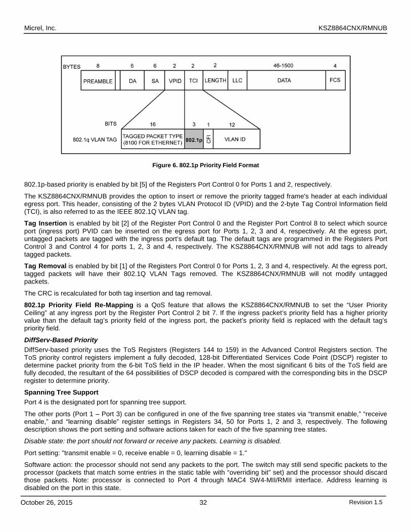
Micrel, Inc. KSZ8864CNX/RMNUB
October 26, 2015 32 Revision 1.5
Figure 6. 802.1p Priority Field Format
802.1p-based priority is enabled by bit [5] of the Registers Port Control 0 for Ports 1 and 2, respectively.
The KSZ8864CNX/RMNUB provides the option to insert or remove the priority tagged frame's header at each individual egress port. This header, consisting of the 2 bytes VLAN Protocol ID (VPID) and the 2-byte Tag Control Information field (TCI), is also referred to as the IEEE 802.1Q VLAN tag.
Tag Insertion is enabled by bit [2] of the Register Port Control 0 and the Register Port Control 8 to select which source port (ingress port) PVID can be inserted on the egress port for Ports 1, 2, 3 and 4, respectively. At the egress port, untagged packets are tagged with the ingress port’s default tag. The default tags are programmed in the Registers Port Control 3 and Control 4 for ports 1, 2, 3 and 4, respectively. The KSZ8864CNX/RMNUB will not add tags to already tagged packets.
Tag Removal is enabled by bit [1] of the Registers Port Control 0 for Ports 1, 2, 3 and 4, respectively. At the egress port, tagged packets will have their 802.1Q VLAN Tags removed. The KSZ8864CNX/RMNUB will not modify untagged packets.
The CRC is recalculated for both tag insertion and tag removal.
802.1p Priority Field Re-Mapping is a QoS feature that allows the KSZ8864CNX/RMNUB to set the “User Priority Ceiling” at any ingress port by the Register Port Control 2 bit 7. If the ingress packet’s priority field has a higher priority value than the default tag’s priority field of the ingress port, the packet’s priority field is replaced with the default tag’s priority field.
DiffServ-Based Priority DiffServ-based priority uses the ToS Registers (Registers 144 to 159) in the Advanced Control Registers section. The ToS priority control registers implement a fully decoded, 128-bit Differentiated Services Code Point (DSCP) register to determine packet priority from the 6-bit ToS field in the IP header. When the most significant 6 bits of the ToS field are fully decoded, the resultant of the 64 possibilities of DSCP decoded is compared with the corresponding bits in the DSCP register to determine priority.
Spanning Tree Support Port 4 is the designated port for spanning tree support.
The other ports (Port 1 – Port 3) can be configured in one of the five spanning tree states via “transmit enable,” “receive enable,” and “learning disable” register settings in Registers 34, 50 for Ports 1, 2 and 3, respectively. The following description shows the port setting and software actions taken for each of the five spanning tree states.
Disable state: the port should not forward or receive any packets. Learning is disabled.
Port setting: "transmit enable = 0, receive enable = 0, learning disable = 1."
Software action: the processor should not send any packets to the port. The switch may still send specific packets to the processor (packets that match some entries in the static table with “overriding bit” set) and the processor should discard those packets. Note: processor is connected to Port 4 through MAC4 SW4-MII/RMII interface. Address learning is disabled on the port in this state.

Micrel, Inc. KSZ8864CNX/RMNUB
October 26, 2015 33 Revision 1.5
Blocking state: only packets to the processor are forwarded. Learning is disabled.
Port setting: "transmit enable = 0, receive enable = 0, learning disable = 1"
Software action: the processor should not send any packets to the port(s) in this state. The processor should program the “Static MAC table” with the entries that it needs to receive (e.g., BPDU packets). The “overriding” bit should also be set so that the switch will forward those specific packets to the processor. Address learning is disabled on the port in this state.
Listening state: only packets to and from the processor are forwarded. Learning is disabled.
Port setting: "transmit enable = 0, receive enable = 0, learning disable = 1.
"Software action: The processor should program the static MAC table with the entries that it needs to receive (e.g., BPDU packets). The “overriding” bit should be set so that the switch will forward those specific packets to the processor. The processor may send packets to the port(s) in this state, see the “Tail Tagging Mode” section for details. Address learning is disabled on the port in this state.
Learning state: only packets to and from the processor are forwarded. Learning is enabled.
Port setting: “transmit enable = 0, receive enable = 0, learning disable = 0.”
Software action: The processor should program the static MAC table with the entries that it needs to receive (e.g., BPDU packets). The “overriding” bit should be set so that the switch will forward those specific packets to the processor. The processor may send packets to the port(s) in this state, see the “Tail Tagging Mode” section for details. Address learning is enabled on the port in this state.
Forwarding state: packets are forwarded and received normally. Learning is enabled.
Port setting: “transmit enable = 1, receive enable = 1, learning disable = 0.”
Software action: The processor should program the static MAC table with the entries that it needs to receive (e.g., BPDU packets). The “overriding” bit should be set so that the switch will forward those specific packets to the processor. The processor may send packets to the port(s) in this state, see “Tail Tagging Mode” section for details. Address learning is enabled on the port in this state.
Rapid Spanning Tree Support There are three operational states of the Discarding, Learning, and Forwarding assigned to each port for RSTP:
Discarding ports Do not participate in the active topology and Do not learn MAC addresses.
Discarding state: the state includes three states of the disable, blocking, and listening of STP.
Port setting: "transmit enable = 0, receive enable = 0, learning disable = 1."
Software action: the processor should not send any packets to the port. The switch may still send specific packets to the processor (packets that match some entries in the static table with “overriding bit” set) and the processor should discard those packets. When disable the port’s learning capability (learning disable=’1’), set the Register 1 bit5 and bit4 will flush rapidly with the port related entries in the dynamic MAC table and static MAC table.
Note: processor is connected to Port 4 MAC 4 SW4-MII/RMII interface. Address learning is disabled on the port in this state.
Ports in Learning states learn MAC addresses, but Do not forward user traffic.
Learning state: only packets to and from the processor are forwarded. Learning is enabled.
Port setting: “transmit enable = 0, receive enable = 0, learning disable = 0.”
Software action: The processor should program the static MAC table with the entries that it needs to receive (e.g., BPDU packets). The “overriding” bit should be set so that the switch will forward those specific packets to the processor. The processor may send packets to the port(s) in this state, see “Tail Tagging Mode” section for details. Address learning is enabled on the port in this state.
Ports in Forwarding states fully participate in both data forwarding and MAC learning.
Forwarding state: packets are forwarded and received normally. Learning is enabled.
Port setting: “transmit enable = 1, receive enable = 1, learning disable = 0.”
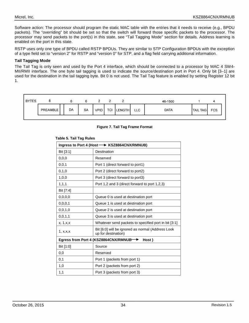
Micrel, Inc. KSZ8864CNX/RMNUB
October 26, 2015 34 Revision 1.5
Software action: The processor should program the static MAC table with the entries that it needs to receive (e.g., BPDU packets). The “overriding” bit should be set so that the switch will forward those specific packets to the processor. The processor may send packets to the port(s) in this state, see “Tail Tagging Mode” section for details. Address learning is enabled on the port in this state.
RSTP uses only one type of BPDU called RSTP BPDUs. They are similar to STP Configuration BPDUs with the exception of a type field set to “version 2” for RSTP and “version 0” for STP, and a flag field carrying additional information.
Tail Tagging Mode The Tail Tag is only seen and used by the Port 4 interface, which should be connected to a processor by MAC 4 SW4-MII/RMII interface. The one byte tail tagging is used to indicate the source/destination port in Port 4. Only bit [3–1] are used for the destination in the tail tagging byte. Bit 0 is not used. The Tail Tag feature is enabled by setting Register 12 bit 1.
Figure 7. Tail Tag Frame Format Table 5. Tail Tag Rules
Ingress to Port 4 (Host KSZ8864CNX/RMNUB)
Bit [3:1] Destination
0,0,0 Reserved
0,0,1 Port 1 (direct forward to port1)
0,1,0 Port 2 (direct forward to port2)
1,0,0 Port 3 (direct forward to port3)
1,1,1 Port 1,2 and 3 (direct forward to port 1,2,3)
Bit [7:4]
0,0,0,0 Queue 0 is used at destination port
0,0,0,1 Queue 1 is used at destination port
0,0,1,0 Queue 2 is used at destination port
0,0,1,1 Queue 3 is used at destination port
x, 1,x,x Whatever send packets to specified port in bit [3:1]
1, x,x,x Bit [6:0] will be ignored as normal (Address Look up for destination)
Egress from Port 4 (KSZ8864CNX/RMNUB Host )
Bit [1:0] Source
0,0 Reserved
0,1 Port 1 (packets from port 1)
1,0 Port 2 (packets from port 2)
1,1 Port 3 (packets from port 3)
Micrel, Inc. KSZ8864CNX/RMNUB
October 26, 2015 35 Revision 1.5
IGMP Support There are two parts involved to support the Internet Group Management Protocol (IGMP) in Layer 2. The first part is IGMP snooping, the second part is this IGMP packet to be sent back to the subscribed port. Describe them as follows.
IGMP Snooping The KSZ8864CNX/RMNUB traps IGMP packets and forwards them only to the processor (Port 4 SW4-MII/RMII). The IGMP packets are identified as IP packets (either Ethernet IP packets, or IEEE 802.3 SNAP IP packets) with IP version = 0x4 and protocol version number = 0x2. Set Register 5 bit [6] to ‘1’ to enable IGMP snooping.
IGMP Send Back to the Subscribed Port Once the host responds the received IGMP packet, the host should know the original IGMP ingress port and send back the IGMP packet to this port only, otherwise this IGMP packet will be broadcasted to all port to downgrade the performance.
Enable the tail tag mode, the host will know the IGMP packet received port from tail tag bits [1:0] and can send back the response IGMP packet to this subscribed port by setting the bits [3:1] in the tail tag. Enable “Tail tag mode” by setting Register 12 bit 1.
Port Mirroring Support KSZ8864CNX/RMNUB supports “port mirror” comprehensively as:
• “Receive Only” Mirror on a Port − All the packets received on the port will be mirrored on the sniffer port. For example, Port 1 is programmed to be
“rx sniff,” and Port 2 is programmed to be the “sniffer port.” A packet, received on Port 1, is destined to Port 3 after the internal look-up. The KSZ8864CNX/RMNUB will forward the packet to both Port 2 and Port 3. KSZ8864CNX/RMNUB can optionally forward even “bad” received packets to Port 3.
• “Transmit Only” Mirror on a Port − All the packets transmitted on the port will be mirrored on the sniffer port. For example, Port 1 is programmed to
be “tx sniff,” and Port 2 is programmed to be the “sniffer port.” A packet, received on any of the ports, is destined to port 1 after the internal look-up. The KSZ8864CNX/RMNUB will forward the packet to both Ports 1 and 2.
• “Receive and Transmit” Mirror on a Port − All the packets received on port A AND transmitted on port B will be mirrored on the sniffer port. To turn on the
“AND” feature, set Register 5 bit 0 to 1. For example, Port 1 is programmed to be “rx sniff and tx sniff,” and Port 2 is programmed to be the “sniffer port.” When received and transmit packets on port 1. The KSZ8864CNX/RMNUB will monitor port 1 packets on Port 2.
Multiple ports can be selected to be “rx sniffed” or “tx sniffed.” And any port can be selected to be the “sniffer port.” All these per port features can be selected through Register 17.
VLAN Support KSZ8864CNX/RMNUB supports 128 active VLANs and 4096 possible VIDs specified in IEEE 802.1q. The KSZ8864CNX/RMNUB provides a 128-entry VLAN table, which correspond to 4096 possible VIDs and converts to FID (7 bits) for address look-up maximum of 128 active VLANs. If a non-tagged or null-VID-tagged packet is received, the ingress port VID is used for look-up when 802.1q is enabled by the global Register 5 control 3 bit 7. In the VLAN mode, the look-up process starts from VLAN table look-up to determine whether the VID is valid. If the VID is not valid, the packet will be dropped and its address will not be learned. If the VID is valid, then FID is retrieved for further look-up by the static MAC table or dynamic MAC table. FID+DA is used to determine the destination port. The followed table describes the difference actions at different situations of DA and FID+DA in the static MAC table and dynamic MAC table after the VLAN table finishes a look-up action. FID+SA is used for learning purposes. Table 6 also describes how to learning in the dynamic MAC table when VLAN table has done a look-up and the static MAC table without a valid entry.
Micrel, Inc. KSZ8864CNX/RMNUB
October 26, 2015 36 Revision 1.5
Table 6. FID+DA Look Up in the VLAN Mode
DA Found in Static MAC Table
USE FID Flag? FID Match?
DA+FID Found in Dynamic MAC
Table Action
No Do not Care Do not Care No Broadcast to the membership ports defined in the VLAN table bit [11:7].
No Do not Care Do not Care Yes Send to the destination port defined in the dynamic MAC table bit [58:56].
Yes 0 Do not Care Do not Care Send to the destination port(s) defined in the static MAC table bit [52:48].
Yes 1 No No Broadcast to the membership ports defined in the VLAN table bit [11:7].
Yes 1 No Yes Send to the destination port defined in the dynamic MAC table bit [58:56].
Yes 1 Yes Do not Care Send to the destination port(s) defined in the static MAC table bit [52:48].
Table 7. FID+SA Look Up in the VLAN Mode
SA+FID Found in Dynamic MAC Table Action
No The SA+FID will be learned into the dynamic table.
Yes Time stamp will be updated.
Advanced VLAN features are also supported in KSZ8864CNX/RMNUB, such as “VLAN ingress filtering” and “discard non PVID” defined in bits [6:5] of the Register Port Control 2. These features can be controlled on a port basis.
Rate Limiting Support The KSZ8864CNX/RMNUB provides a fine resolution hardware rate limiting. The rate step is 64Kbps when the rate limit is less than 1Mbps rate for 100BT or 10BT. The rate step is 1Mbps when the rate limit is more than 1Mbps rate for 100BT or 10BT (refer to Data Rate Selection Table which follow the end of the Port Register Queue 0–3 Ingress/Egress Limit Control section). The rate limit is independently on the “receive side” and on the “transmit side” on a per port basis. For 10BASE-T, a rate setting above 10Mbps means the rate is not limited. On the receive side, the data receive rate for each priority at each port can be limited by setting up Ingress Rate Control Registers. On the transmit side, the data transmit rate for each priority queue at each port can be limited by setting up Egress Rate Control Registers. The size of each frame has options to include minimum IFG (Inter Frame Gap) or Preamble byte, in addition to the data field (from packet DA to FCS).
Ingress Rate Limit For ingress rate limiting, KSZ8864CNX/RMNUB provides options to selectively choose frames from all types, multicast, broadcast, and flooded unicast frames by bits [3–2] of the port rate limit control register. The KSZ8864CNX/RMNUB counts the data rate from those selected type of frames. Packets are dropped at the ingress port when the data rate exceeds the specified rate limit or when the flow control takes effect without packet dropped. This occurs when the ingress rate limit flow control is enabled by the port rate limit control register bit 4. The ingress rate limiting supports the port-based, 802.1p and DiffServ-based priorities, the port-based priority is fixed priority 0–3 selection by bits [4–3] of the Register Port Control 0. The 802.1p and DiffServ-based priority can be mapped to priority 0–3 by default of the Register 128 and 129. In the ingress rate limit, set Register 135 Global Control 19 bit3 in order for the queue-based rate limit to be enabled if use two queues or four queues mode, all related ingress ports and egress port should be split into two or four queues mode by the Registers Port Control 9 and Control 0. The four queues mode will use Q0–Q3 for priority 0–3 by bit [6-0] of the port Register ingress limit control 1–4. The two queues mode will use Q0–Q1 for priority 0–1 by bit [6–0] of the port Register ingress limit control 1–2.
The priority levels in the packets of the 802.1p and DiffServ can be programmed to priority 0-3 by the Register 128 and 129 for a re-mapping.

Micrel, Inc. KSZ8864CNX/RMNUB
October 26, 2015 37 Revision 1.5
Egress Rate Limit For egress rate limiting, the Leaky Bucket algorithm is applied to each output priority queue for shaping output traffic. Inter frame gap is stretched on a per frame base to generate smooth, non-burst egress traffic. The throughput of each output priority queue is limited by the egress rate specified by the data rate selection table followed the egress rate limit control registers.
If any egress queue receives more traffic than the specified egress rate throughput, packets may be accumulated in the output queue and packet memory. After the memory of the queue or the port is used up, packet dropping or flow control will be triggered. As a result of congestion, the actual egress rate may be dominated by flow control/dropping at the ingress end, and may be therefore slightly less than the specified egress rate. The egress rate limiting supports the port-based, 802.1p and DiffServ-based priorities, the port-based priority is fixed priority 0–3 selection by bits [4–3] of the Register Port Control 0. The 802.1p and DiffServ-based priority can be mapped to priority 0–3 by default of the Register 128 and 129. In the egress rate limit, set Register 135 global control 19 bit3 for queue-based rate limit to be enabled if using two queues or four queues mode. All related ingress ports and egress port should be split into two or four queues mode by the Registers Port Control 9 and Control 0. The four queues mode will use Q0-Q3 for priority 0-3 by bit [6-0] of the port Register egress limit control 1–4. The two queues mode will use Q0–Q1 for priority 0–1 by bit [6–0] of the port Register egress limit control 1–2. The priority levels in the packets of the 802.1p and DiffServ can be programmed to priority 0–3 by the Register 128 and 129 for a re-mapping.
With egress rate limit just use one queue per port for the egress port rate limit, the priority packets will be based on the data rate selection table with the rate limit exact number. If egress rate limit use more than one queue per port for the egress port rate limit, the highest priority packets will be based on the data rate selection table for the rate limit exact number and other lower priority packet rate will be limited based on 8:4:2:1 (default) priority ratio based on the highest priority rate. The transmit queue priority ratio is programmable.
To reduce congestion, it is a good practice to make sure the egress bandwidth exceeds the ingress bandwidth.
Transmit Queue Ratio Programming In transmit queues 0-3 of the egress port, the default priority ratio is 8:4:2:1, the priority ratio can be programmed by the Registers Port Control 10, 11, 12, and 13. When the transmit rate exceed the ratio limit in the transmit queue, the transmit rate will be limited by the transmit queue 0-3 ratio of the Register Port Control 10, 11, 12, and 13. The highest priority queue will be no limited, other lower priority queues will be limited based on the transmit queue ratio.
Filtering for Self-Address, Unknown Unicast/Multicast Address and Unknown VID Packet/IP Multicast Enable Self-address filtering, the unknown unicast packet filtering and forwarding by the Register 131 Global Control 15.
Enable Unknown multicast packet filtering and forwarding by the Register 132 Global Control 16.
Enable Unknown VID packet filtering and forwarding by the Register 133 Global Control 17.
Enable Unknown IP multicast packet filtering and forwarding by the Register 134 Global Control 18.
This function is very useful in preventing those kinds of packets that could degrade the quality of the port in applications such as voice over Internet Protocol (VoIP) and the daisy chain connection to prevent packets into endless loop.
Configuration Interface
I2C Master Serial Bus Configuration If a 2-wire EEPROM exists, the KSZ8864CNX/RMNUB can perform more advanced features like broadcast storm protection and rate control. The EEPROM should have the entire valid configuration data from Register 0 to Register 255 defined in the “Memory Map,” except the status registers and indirect registers. After reset, the KSZ8864CNX/RMNUB will start to read all control registers sequentially from the EEPROM. The configuration access time (tprgm) is less than 30ms, as shown in Figure 8.
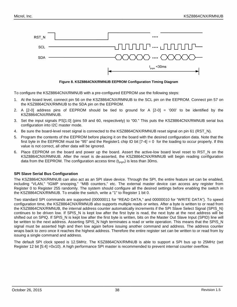
Micrel, Inc. KSZ8864CNX/RMNUB
October 26, 2015 38 Revision 1.5
Figure 8. KSZ8864CNX/RMNUB EEPROM Configuration Timing Diagram
To configure the KSZ8864CNX/RMNUB with a pre-configured EEPROM use the following steps:
1. At the board level, connect pin 56 on the KSZ8864CNX/RMNUB to the SCL pin on the EEPROM. Connect pin 57 on the KSZ8864CNX/RMNUB to the SDA pin on the EEPROM.
2. A [2-0] address pins of EEPROM should be tied to ground for A [2-0] = ‘000’ to be identified by the KSZ8864CNX/RMNUB.
3. Set the input signals PS[1:0] (pins 59 and 60, respectively) to “00.” This puts the KSZ8864CNX/RMNUB serial bus configuration into I2C master mode.
4. Be sure the board-level reset signal is connected to the KSZ8864CNX/RMNUB reset signal on pin 61 (RST_N). 5. Program the contents of the EEPROM before placing it on the board with the desired configuration data. Note that the
first byte in the EEPROM must be “95” and the Register1 chip ID bit [7-4] = 0 for the loading to occur properly. If this value is not correct, all other data will be ignored.
6. Place EEPROM on the board and power up the board. Assert the active-low board level reset to RST_N on the KSZ8864CNX/RMNUB. After the reset is de-asserted, the KSZ8864CNX/RMNUB will begin reading configuration data from the EEPROM. The configuration access time (tprgm) is less than 30ms.
SPI Slave Serial Bus Configuration The KSZ8864CNX/RMNUB can also act as an SPI slave device. Through the SPI, the entire feature set can be enabled, including “VLAN,” “IGMP snooping,” “MIB counters,” etc. The external master device can access any register from Register 0 to Register 255 randomly. The system should configure all the desired settings before enabling the switch in the KSZ8864CNX/RMNUB. To enable the switch, write a "1" to Register 1 bit 0.
Two standard SPI commands are supported (00000011 for “READ DATA,” and 00000010 for “WRITE DATA”). To speed configuration time, the KSZ8864CNX/RMNUB also supports multiple reads or writes. After a byte is written to or read from the KSZ8864CNX/RMNUB, the internal address counter automatically increments if the SPI Slave Select Signal (SPIS_N) continues to be driven low. If SPIS_N is kept low after the first byte is read, the next byte at the next address will be shifted out on SPIQ. If SPIS_N is kept low after the first byte is written, bits on the Master Out Slave Input (SPID) line will be written to the next address. Asserting SPIS_N high terminates a read or write operation. This means that the SPIS_N signal must be asserted high and then low again before issuing another command and address. The address counter wraps back to zero once it reaches the highest address. Therefore the entire register set can be written to or read from by issuing a single command and address.
The default SPI clock speed is 12.5MHz. The KSZ8864CNX/RMNUB is able to support a SPI bus up to 25MHz (set Register 12 bit [5:4] =0x10). A high performance SPI master is recommended to prevent internal counter overflow.
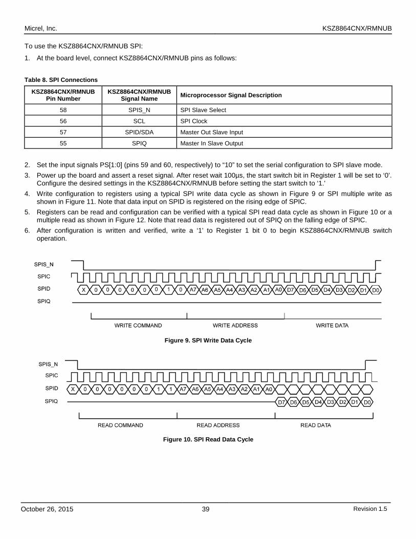
Micrel, Inc. KSZ8864CNX/RMNUB
October 26, 2015 39 Revision 1.5
To use the KSZ8864CNX/RMNUB SPI:
1. At the board level, connect KSZ8864CNX/RMNUB pins as follows: Table 8. SPI Connections
KSZ8864CNX/RMNUB Pin Number
KSZ8864CNX/RMNUB Signal Name Microprocessor Signal Description
58 SPIS_N SPI Slave Select
56 SCL SPI Clock
57 SPID/SDA Master Out Slave Input
55 SPIQ Master In Slave Output
2. Set the input signals PS[1:0] (pins 59 and 60, respectively) to “10” to set the serial configuration to SPI slave mode. 3. Power up the board and assert a reset signal. After reset wait 100µs, the start switch bit in Register 1 will be set to ‘0’.
Configure the desired settings in the KSZ8864CNX/RMNUB before setting the start switch to ‘1.' 4. Write configuration to registers using a typical SPI write data cycle as shown in Figure 9 or SPI multiple write as
shown in Figure 11. Note that data input on SPID is registered on the rising edge of SPIC. 5. Registers can be read and configuration can be verified with a typical SPI read data cycle as shown in Figure 10 or a
multiple read as shown in Figure 12. Note that read data is registered out of SPIQ on the falling edge of SPIC. 6. After configuration is written and verified, write a ‘1’ to Register 1 bit 0 to begin KSZ8864CNX/RMNUB switch
operation.
Figure 9. SPI Write Data Cycle
Figure 10. SPI Read Data Cycle
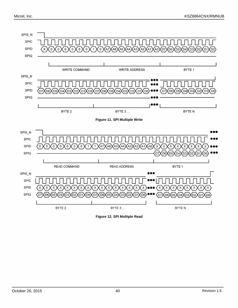
Micrel, Inc. KSZ8864CNX/RMNUB
October 26, 2015 40 Revision 1.5
Figure 11. SPI Multiple Write
Figure 12. SPI Multiple Read
Micrel, Inc. KSZ8864CNX/RMNUB
October 26, 2015 41 Revision 1.5
MII Management Interface (MIIM) The KSZ8864CNX/RMNUB supports the standard IEEE 802.3 MII Management Interface, also known as the Management Data Input/output (MDIO) Interface. This interface allows upper-layer devices to monitor and control the states of the KSZ8864CNX/RMNUB. An external device with MDC/MDIO capability is used to read the PHY status or configure the PHY settings. Further detail on the MIIM interface is found in Clause 22.2.4.5 of the IEEE 802.3u specification.
The MIIM interface consists of the following:
• A physical connection that incorporates the data line (pin 54 MDIO) and the clock line (pin 53 MDC). • A specific protocol that operates across the aforementioned physical connection that allows an external controller to
communicate with the KSZ8864CNX/RMNUB device. • Access to a set of eight 16-bit registers, consisting of 8 standard MIIM Registers [0:5h], 1d and 1f MIIM registers per
port.
The MIIM Interface can operate up to a maximum clock speed of 10MHz MDC clock.
Table 9 depicts the MII Management Interface frame format.
Table 9. MII Management Interface Frame Format
Preamble Start of Frame Read/Write OP Code
PHY Address Bits [4:0]
REG Address Bits [4:0]
TA Data Bits [15:0] Idle
Read 32 1’s 01 10 AAAAA RRRRR Z0 DDDDDDDD_DDDDDDDD Z
Write 32 1’s 01 01 AAAAA RRRRR 10 DDDDDDDD_DDDDDDDD Z
The MIIM interface does not have access to all the configuration registers in the KSZ8864CNX/RMNUB. It can only access the standard MIIM registers. See “MIIM Registers”. The SPI interface and MDC/MDIO SMI mode, on the other hand, can be used to access the entire KSZ8864CNX/RMNUB feature set.
Serial Management Interface (SMI) The SMI is the KSZ8864CNX/RMNUB non-standard MIIM interface that provides access to all KSZ8864CNX/RMNUB configuration registers. This interface allows an external device with MDC/MDIO interface to completely monitor and control the states of the KSZ8864CNX/RMNUB.
The SMI interface consists of the following:
• A physical connection that incorporates the data line (MDIO) and the clock line (MDC). • A specific protocol that operates across the aforementioned physical connection that allows an external controller to
communicate with the KSZ8864CNX/RMNUB device. • Access all KSZ8864CNX/RMNUB configuration registers. Register access includes the Global, Port and Advanced
Control Registers 0-255 (0x00 – 0xFF), and indirect access to the standard MIIM Registers [0:5] and custom MIIM Registers [29, 31].
The SMI Interface can operate up to a maximum clock speed of 10MHz MDC clock.
Table 10 depicts the SMI frame format.
Table 10. Serial Management Interface (SMI) Frame Format
Preamble Start of Frame Read/Write OP Code
PHY Address Bits [4:0]
REG Address Bits [4:0]
TA Data Bits [15:0] Idle
Read 32 1’s 01 10 RR11R RRRRR Z0 0000_0000_DDDD_DDDD Z
Write 32 1’s 01 01 RR11R RRRRR 10 xxxx_xxxx_DDDD_DDDD Z
Micrel, Inc. KSZ8864CNX/RMNUB
October 26, 2015 42 Revision 1.5
SMI register read access is selected when OP code is set to “10” and bits [2:1] of the PHY address is set to ‘11’. The 8-bit register address is the concatenation of PHY address bits [4:3], PHY address bits [0], REG address bit [4:0]. TA is turn-around bits. TA bits [1:0] are ’Z0’ means the processor MDIO pin is changed to input Hi-Z from output mode and the followed ‘0’ is the read response from device, as the switch configuration registers are 8-bit wide, only the lower 8 bits of data bits [15:0] are used
SMI register Write access is selected when OP Code is set to “01” and bits [2:1] of the PHY address is set to ‘11’. The 8-bit register address is the concatenation of PHY address bits [4:3], PHY address bits [0], REG address bit [4:0]. TA bits [1:0] are set to ’10’, as the switch configuration registers are 8-bit wide, only the lower 8 bits of data bits [15:0] are used.
To access the KSZ8864CNX/RMNUB Registers 0-255 (0x00 – 0xFF), the following applies:
• PHYAD [4, 3, 0] and REGAD [4:0] are concatenated to form the 8-bit address; that is, PHYAD [4, 3, 0], REGAD [4:0] = bits [7:0] of the 8-bit address.
• Registers are eight data bits wide. For read operation, data bits [15:8] are read back as 0’s. For write operation, data bits [15:8] are not defined, and hence can be set to either 0s or 1s.
SMI register access is the same as the MIIM register access, except for the register access requirements presented in this section.
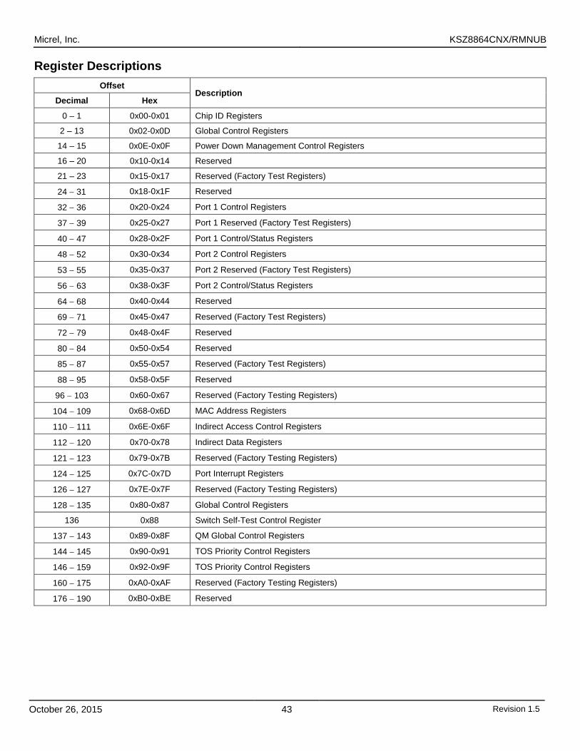
Micrel, Inc. KSZ8864CNX/RMNUB
October 26, 2015 43 Revision 1.5
Register Descriptions Offset
Description Decimal Hex
0 – 1 0x00-0x01 Chip ID Registers
2 – 13 0x02-0x0D Global Control Registers
14 – 15 0x0E-0x0F Power Down Management Control Registers
16 – 20 0x10-0x14 Reserved
21 – 23 0x15-0x17 Reserved (Factory Test Registers)
24 − 31 0x18-0x1F Reserved
32 − 36 0x20-0x24 Port 1 Control Registers
37 − 39 0x25-0x27 Port 1 Reserved (Factory Test Registers)
40 − 47 0x28-0x2F Port 1 Control/Status Registers
48 − 52 0x30-0x34 Port 2 Control Registers
53 − 55 0x35-0x37 Port 2 Reserved (Factory Test Registers)
56 − 63 0x38-0x3F Port 2 Control/Status Registers
64 − 68 0x40-0x44 Reserved
69 − 71 0x45-0x47 Reserved (Factory Test Registers)
72 − 79 0x48-0x4F Reserved
80 − 84 0x50-0x54 Reserved
85 − 87 0x55-0x57 Reserved (Factory Test Registers)
88 − 95 0x58-0x5F Reserved
96 − 103 0x60-0x67 Reserved (Factory Testing Registers)
104 − 109 0x68-0x6D MAC Address Registers
110 − 111 0x6E-0x6F Indirect Access Control Registers
112 − 120 0x70-0x78 Indirect Data Registers
121 − 123 0x79-0x7B Reserved (Factory Testing Registers)
124 − 125 0x7C-0x7D Port Interrupt Registers
126 − 127 0x7E-0x7F Reserved (Factory Testing Registers)
128 − 135 0x80-0x87 Global Control Registers
136 0x88 Switch Self-Test Control Register
137 − 143 0x89-0x8F QM Global Control Registers
144 − 145 0x90-0x91 TOS Priority Control Registers
146 − 159 0x92-0x9F TOS Priority Control Registers
160 − 175 0xA0-0xAF Reserved (Factory Testing Registers)
176 − 190 0xB0-0xBE Reserved
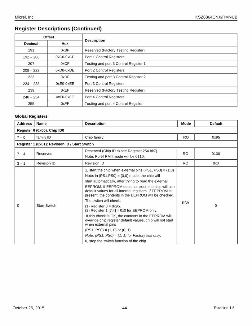
Micrel, Inc. KSZ8864CNX/RMNUB
October 26, 2015 44 Revision 1.5
Register Descriptions (Continued) Offset
Description Decimal Hex
191 0xBF Reserved (Factory Testing Register)
192 − 206 0xC0-0xCE Port 1 Control Registers
207 0xCF Testing and port 3 Control Register 1
208 − 222 0xD0-0xDE Port 2 Control Registers
223 0xDF Testing and port 3 Control Register 2
224 − 238 0xE0-0xEE Port 3 Control Registers
239 0xEF Reserved (Factory Testing Register)
240 − 254 0xF0-0xFE Port 4 Control Registers
255 0xFF Testing and port 4 Control Register
Global Registers
Address Name Description Mode Default
Register 0 (0x00): Chip ID0
7 − 0 family ID Chip family. RO 0x95
Register 1 (0x01): Revision ID / Start Switch
7 − 4 Reserved Reserved (Chip ID to see Register 254 bit7) Note: Port4 RMII mode will be 0110.
RO 0100
3 − 1 Revision ID Revision ID RO 0x0
0 Start Switch
1, start the chip when external pins (PS1, PS0) = (1,0) Note: in (PS1,PS0) = (0,0) mode, the chip will start automatically, after trying to read the external EEPROM. If EEPROM does not exist, the chip will use default values for all internal registers. If EEPROM is present, the contents in the EEPROM will be checked. The switch will check: (1) Register 0 = 0x95. (2) Register 1 [7:4] = 0x0 for EEPROM only. If this check is OK, the contents in the EEPROM will override chip register default values, chip will not start when external pins (PS1, PS0) = (1, 0) or (0, 1). Note: (PS1, PS0) = (1, 1) for Factory test only. 0, stop the switch function of the chip
R/W
0
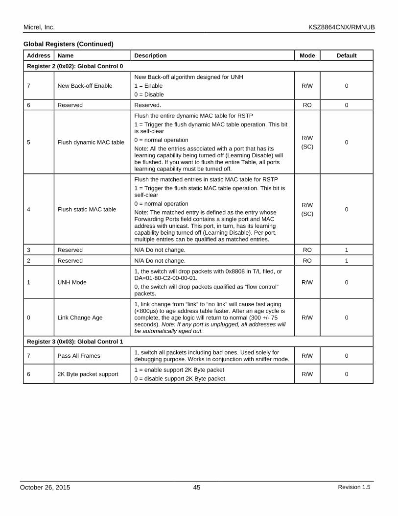
Micrel, Inc. KSZ8864CNX/RMNUB
October 26, 2015 45 Revision 1.5
Global Registers (Continued)
Address Name Description Mode Default
Register 2 (0x02): Global Control 0
7 New Back-off Enable New Back-off algorithm designed for UNH 1 = Enable 0 = Disable
R/W 0
6 Reserved Reserved. RO 0
5 Flush dynamic MAC table
Flush the entire dynamic MAC table for RSTP 1 = Trigger the flush dynamic MAC table operation. This bit is self-clear 0 = normal operation Note: All the entries associated with a port that has its learning capability being turned off (Learning Disable) will be flushed. If you want to flush the entire Table, all ports learning capability must be turned off.
R/W (SC)
0
4 Flush static MAC table
Flush the matched entries in static MAC table for RSTP 1 = Trigger the flush static MAC table operation. This bit is self-clear 0 = normal operation Note: The matched entry is defined as the entry whose Forwarding Ports field contains a single port and MAC address with unicast. This port, in turn, has its learning capability being turned off (Learning Disable). Per port, multiple entries can be qualified as matched entries.
R/W (SC)
0
3 Reserved N/A Do not change. RO 1
2 Reserved N/A Do not change. RO 1
1 UNH Mode
1, the switch will drop packets with 0x8808 in T/L filed, or DA=01-80-C2-00-00-01. 0, the switch will drop packets qualified as “flow control” packets.
R/W 0
0 Link Change Age
1, link change from “link” to “no link” will cause fast aging (<800µs) to age address table faster. After an age cycle is complete, the age logic will return to normal (300 +/- 75 seconds). Note: If any port is unplugged, all addresses will be automatically aged out.
R/W 0
Register 3 (0x03): Global Control 1
7 Pass All Frames 1, switch all packets including bad ones. Used solely for debugging purpose. Works in conjunction with sniffer mode. R/W 0
6 2K Byte packet support 1 = enable support 2K Byte packet 0 = disable support 2K Byte packet
R/W 0
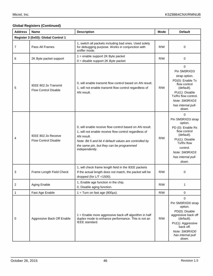
Micrel, Inc. KSZ8864CNX/RMNUB
October 26, 2015 46 Revision 1.5
Global Registers (Continued)
Address Name Description Mode Default
Register 3 (0x03): Global Control 1
7 Pass All Frames 1, switch all packets including bad ones. Used solely for debugging purpose. Works in conjunction with sniffer mode.
R/W 0
6 2K Byte packet support 1 = enable support 2K Byte packet 0 = disable support 2K Byte packet
R/W 0
5 IEEE 802.3x Transmit Flow Control Disable
0, will enable transmit flow control based on AN result. 1, will not enable transmit flow control regardless of AN result.
R/W
0 Pin SM3RXD3 strap option.
PD(0): Enable Tx flow control
(default). PU(1): Disable
Tx/Rx flow control. Note: SM3RXD3 has internal pull-
down.
4 IEEE 802.3x Receive Flow Control Disable
0, will enable receive flow control based on AN result. 1, will not enable receive flow control regardless of AN result. Note: Bit 5 and bit 4 default values are controlled by the same pin, but they can be programmed independently.
R/W
0 Pin SM3RXD3 strap
option. PD (0): Enable Rx
flow control (default).
PU(1): Disable Tx/Rx flow
control. Note: SM3RXD3 has internal pull-
down.
3 Frame Length Field Check 1, will check frame length field in the IEEE packets If the actual length does not match, the packet will be dropped (for L/T <1500).
R/W 0
2 Aging Enable 1, Enable age function in the chip. 0, Disable aging function.
R/W 1
1 Fast Age Enable 1 = Turn on fast age (800µs). R/W 0
0 Aggressive Back Off Enable 1 = Enable more aggressive back-off algorithm in half duplex mode to enhance performance. This is not an IEEE standard.
R/W
0 Pin SM3RXD0 strap
option. PD(0): Disable
aggressive back off (default).
PU(1): Aggressive back off.
Note: SM3RXD0 has internal pull
down.
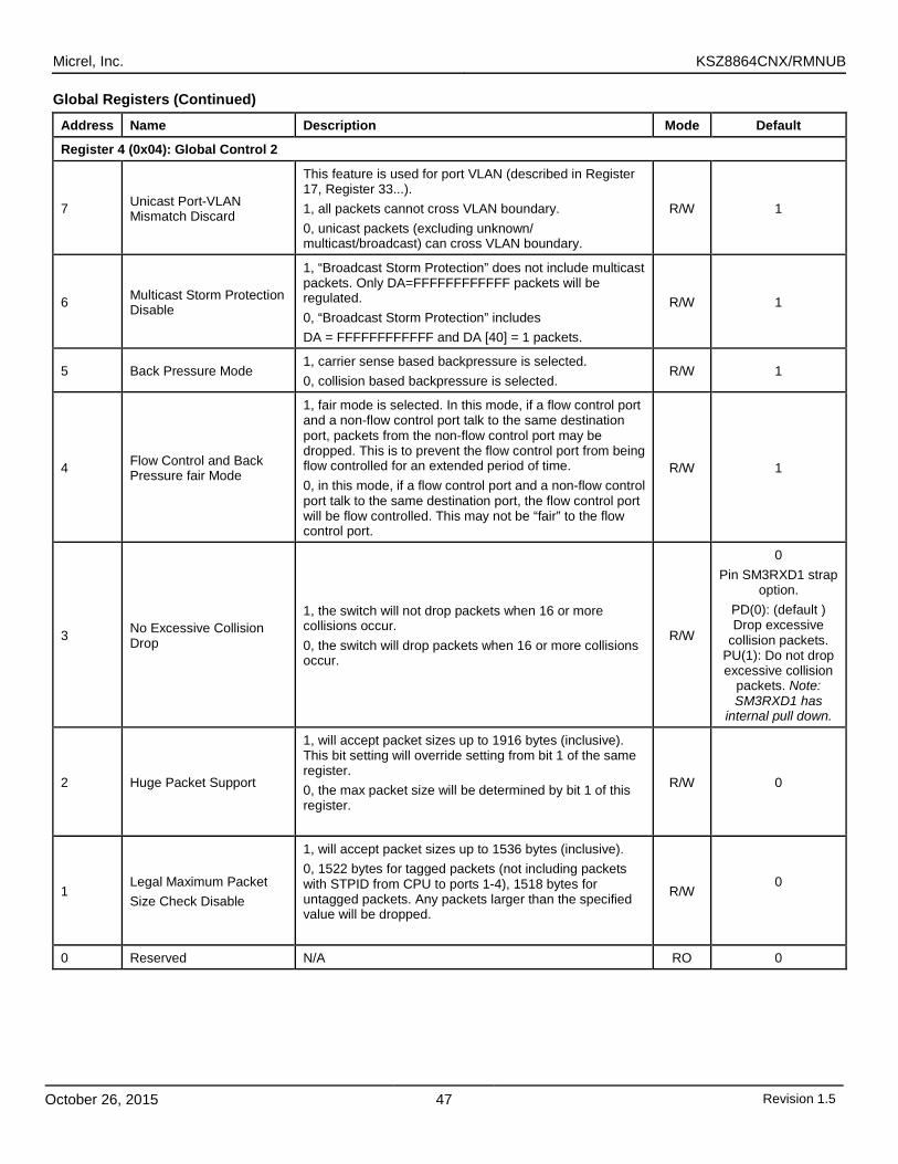
Micrel, Inc. KSZ8864CNX/RMNUB
October 26, 2015 47 Revision 1.5
Global Registers (Continued) Address Name Description Mode Default
Register 4 (0x04): Global Control 2
7 Unicast Port-VLAN Mismatch Discard
This feature is used for port VLAN (described in Register 17, Register 33...). 1, all packets cannot cross VLAN boundary. 0, unicast packets (excluding unknown/ multicast/broadcast) can cross VLAN boundary.
R/W 1
6 Multicast Storm Protection Disable
1, “Broadcast Storm Protection” does not include multicast packets. Only DA=FFFFFFFFFFFF packets will be regulated. 0, “Broadcast Storm Protection” includes DA = FFFFFFFFFFFF and DA [40] = 1 packets.
R/W 1
5 Back Pressure Mode 1, carrier sense based backpressure is selected. 0, collision based backpressure is selected.
R/W 1
4 Flow Control and Back Pressure fair Mode
1, fair mode is selected. In this mode, if a flow control port and a non-flow control port talk to the same destination port, packets from the non-flow control port may be dropped. This is to prevent the flow control port from being flow controlled for an extended period of time. 0, in this mode, if a flow control port and a non-flow control port talk to the same destination port, the flow control port will be flow controlled. This may not be “fair” to the flow control port.
R/W 1
3 No Excessive Collision Drop
1, the switch will not drop packets when 16 or more collisions occur. 0, the switch will drop packets when 16 or more collisions occur.
R/W
0 Pin SM3RXD1 strap
option. PD(0): (default ) Drop excessive
collision packets. PU(1): Do not drop excessive collision
packets. Note: SM3RXD1 has
internal pull down.
2 Huge Packet Support
1, will accept packet sizes up to 1916 bytes (inclusive). This bit setting will override setting from bit 1 of the same register. 0, the max packet size will be determined by bit 1 of this register.
R/W 0
1 Legal Maximum Packet Size Check Disable
1, will accept packet sizes up to 1536 bytes (inclusive). 0, 1522 bytes for tagged packets (not including packets with STPID from CPU to ports 1-4), 1518 bytes for untagged packets. Any packets larger than the specified value will be dropped.
R/W 0
0 Reserved N/A RO 0
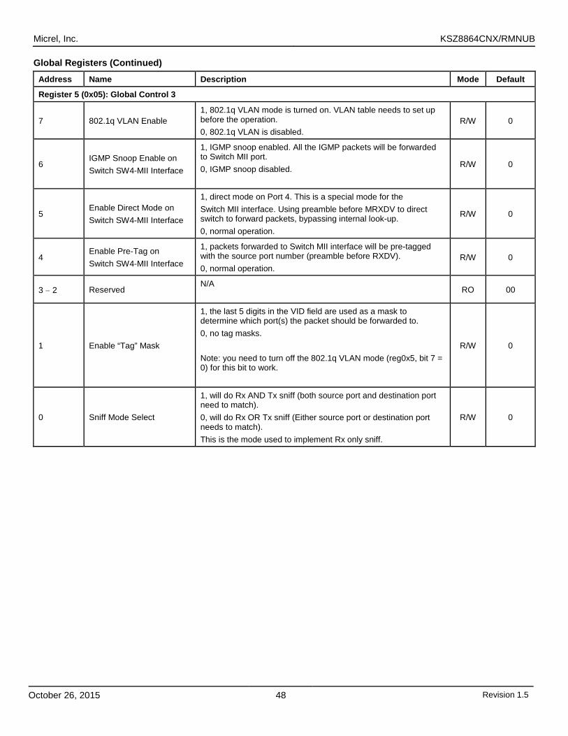
Micrel, Inc. KSZ8864CNX/RMNUB
October 26, 2015 48 Revision 1.5
Global Registers (Continued)
Address Name Description Mode Default
Register 5 (0x05): Global Control 3
7 802.1q VLAN Enable 1, 802.1q VLAN mode is turned on. VLAN table needs to set up before the operation. 0, 802.1q VLAN is disabled.
R/W 0
6 IGMP Snoop Enable on Switch SW4-MII Interface
1, IGMP snoop enabled. All the IGMP packets will be forwarded to Switch MII port. 0, IGMP snoop disabled.
R/W 0
5 Enable Direct Mode on Switch SW4-MII Interface
1, direct mode on Port 4. This is a special mode for the Switch MII interface. Using preamble before MRXDV to direct switch to forward packets, bypassing internal look-up. 0, normal operation.
R/W 0
4 Enable Pre-Tag on Switch SW4-MII Interface
1, packets forwarded to Switch MII interface will be pre-tagged with the source port number (preamble before RXDV). 0, normal operation.
R/W 0
3 − 2 Reserved N/A
RO 00
1 Enable “Tag” Mask
1, the last 5 digits in the VID field are used as a mask to determine which port(s) the packet should be forwarded to. 0, no tag masks. Note: you need to turn off the 802.1q VLAN mode (reg0x5, bit 7 = 0) for this bit to work.
R/W 0
0 Sniff Mode Select
1, will do Rx AND Tx sniff (both source port and destination port need to match). 0, will do Rx OR Tx sniff (Either source port or destination port needs to match). This is the mode used to implement Rx only sniff.
R/W 0
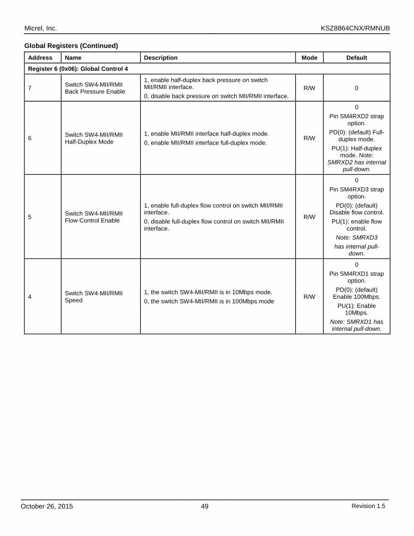
Micrel, Inc. KSZ8864CNX/RMNUB
October 26, 2015 49 Revision 1.5
Global Registers (Continued)
Address Name Description Mode Default
Register 6 (0x06): Global Control 4
7 Switch SW4-MII/RMII Back Pressure Enable
1, enable half-duplex back pressure on switch MII/RMII interface. 0, disable back pressure on switch MII/RMII interface.
R/W 0
6 Switch SW4-MII/RMII Half-Duplex Mode
1, enable MII/RMII interface half-duplex mode. 0, enable MII/RMII interface full-duplex mode.
R/W
0 Pin SM4RXD2 strap
option. PD(0): (default) Full-
duplex mode. PU(1): Half-duplex
mode. Note: SMRXD2 has internal
pull-down.
5 Switch SW4-MII/RMII Flow Control Enable
1, enable full-duplex flow control on switch MII/RMII interface. 0, disable full-duplex flow control on switch MII/RMII interface.
R/W
0 Pin SM4RXD3 strap
option. PD(0): (default)
Disable flow control. PU(1): enable flow
control. Note: SMRXD3 has internal pull-
down.
4 Switch SW4-MII/RMII Speed
1, the switch SW4-MII/RMII is in 10Mbps mode. 0, the switch SW4-MII/RMII is in 100Mbps mode
R/W
0 Pin SM4RXD1 strap
option. PD(0): (default)
Enable 100Mbps. PU(1): Enable
10Mbps. Note: SMRXD1 has internal pull-down.
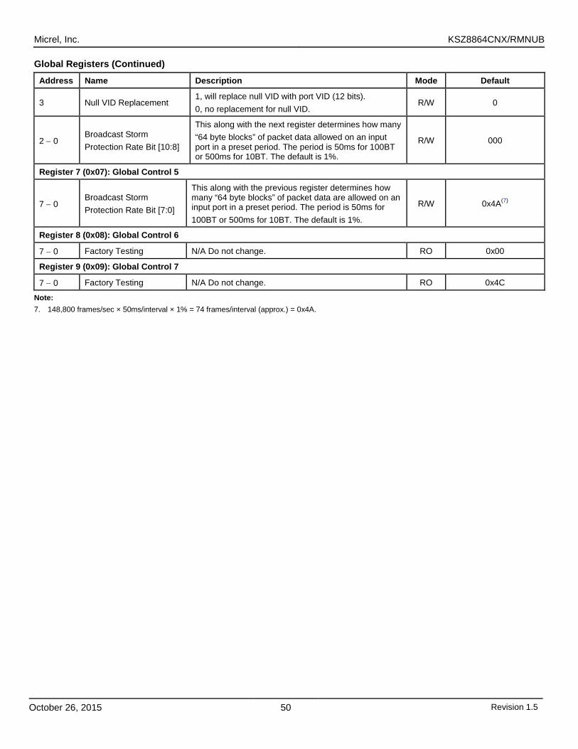
Micrel, Inc. KSZ8864CNX/RMNUB
October 26, 2015 50 Revision 1.5
Global Registers (Continued)
Address Name Description Mode Default
3 Null VID Replacement 1, will replace null VID with port VID (12 bits). 0, no replacement for null VID.
R/W 0
2 − 0 Broadcast Storm Protection Rate Bit [10:8]
This along with the next register determines how many “64 byte blocks” of packet data allowed on an input port in a preset period. The period is 50ms for 100BT or 500ms for 10BT. The default is 1%.
R/W 000
Register 7 (0x07): Global Control 5
7 − 0 Broadcast Storm Protection Rate Bit [7:0]
This along with the previous register determines how many “64 byte blocks” of packet data are allowed on an input port in a preset period. The period is 50ms for 100BT or 500ms for 10BT. The default is 1%.
R/W 0x4A(7)
Register 8 (0x08): Global Control 6
7 − 0 Factory Testing N/A Do not change. RO 0x00
Register 9 (0x09): Global Control 7
7 − 0 Factory Testing N/A Do not change. RO 0x4C
Note: 7. 148,800 frames/sec × 50ms/interval × 1% = 74 frames/interval (approx.) = 0x4A.
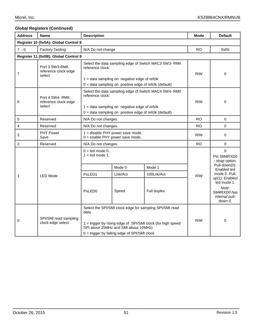
Micrel, Inc. KSZ8864CNX/RMNUB
October 26, 2015 51 Revision 1.5
Global Registers (Continued)
Address Name Description Mode Default
Register 10 (0x0A): Global Control 8
7 − 0 Factory Testing N/A Do not change RO 0x00
Register 11 (0x0B): Global Control 9
7
Port 3 SW3-RMII reference clock edge select
Select the data sampling edge of Switch MAC3 SW3- RMII reference clock: 1 = data sampling on negative edge of refclk 0 = data sampling on positive edge of refclk (default)
R/W 0
6 Port 4 SW4- RMII reference clock edge select
Select the data sampling edge of Switch MAC4 SW4- RMII reference clock: 1 = data sampling on negative edge of refclk 0 = data sampling on positive edge of refclk (default)
R/W 0
5 Reserved N/A Do not changes. RO 0
4 Reserved N/A Do not changes. RO 0
3 PHY Power Save
1 = disable PHY power save mode. 0 = enable PHY power save mode. R/W 0
2 Reserved N/A Do not changes. RO 0
1 LED Mode
0 = led mode 0. 1 = led mode 1.
R/W
0 Pin SM4RXD0 - strap option. Pull-down(0): Enabled led
mode 0. Pull-up(1): Enabled
led mode 1. Note:
SM4RXD0 has internal pull-
down 0.
Mode 0 Mode 1
PxLED1 Link/Act 100Lnk/Act
PxLED0 Speed Full duplex
0 SPI/SMI read sampling clock edge select
Select the SPI/SMI clock edge for sampling SPI/SMI read data 1 = trigger by rising edge of SPI/SMI clock (for high speed SPI about 25MHz and SMI about 10MHz) 0 = trigger by falling edge of SPI/SMI clock
R/W 0
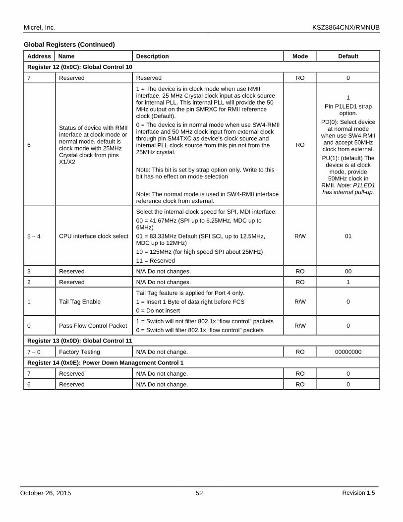
Micrel, Inc. KSZ8864CNX/RMNUB
October 26, 2015 52 Revision 1.5
Global Registers (Continued)
Address Name Description Mode Default
Register 12 (0x0C): Global Control 10
7 Reserved Reserved RO 0
6
Status of device with RMII interface at clock mode or normal mode, default is clock mode with 25MHz Crystal clock from pins X1/X2
1 = The device is in clock mode when use RMII interface, 25 MHz Crystal clock input as clock source for internal PLL. This internal PLL will provide the 50 MHz output on the pin SMRXC for RMII reference clock (Default). 0 = The device is in normal mode when use SW4-RMII interface and 50 MHz clock input from external clock through pin SM4TXC as device’s clock source and internal PLL clock source from this pin not from the 25MHz crystal. Note: This bit is set by strap option only. Write to this bit has no effect on mode selection Note: The normal mode is used in SW4-RMII interface reference clock from external.
RO
1 Pin P1LED1 strap
option. PD(0): Select device
at normal mode when use SW4-RMII and accept 50MHz clock from external. PU(1): (default) The
device is at clock mode, provide 50MHz clock in
RMII. Note: P1LED1 has internal pull-up.
5 − 4 CPU interface clock select
Select the internal clock speed for SPI, MDI interface: 00 = 41.67MHz (SPI up to 6.25MHz, MDC up to 6MHz) 01 = 83.33MHz Default (SPI SCL up to 12.5MHz, MDC up to 12MHz) 10 = 125MHz (for high speed SPI about 25MHz) 11 = Reserved
R/W 01
3 Reserved N/A Do not changes. RO 00
2 Reserved N/A Do not changes. RO 1
1 Tail Tag Enable Tail Tag feature is applied for Port 4 only. 1 = Insert 1 Byte of data right before FCS 0 = Do not insert
R/W 0
0 Pass Flow Control Packet 1 = Switch will not filter 802.1x “flow control” packets 0 = Switch will filter 802.1x “flow control” packets
R/W 0
Register 13 (0x0D): Global Control 11
7 − 0 Factory Testing N/A Do not change. RO 00000000
Register 14 (0x0E): Power Down Management Control 1
7 Reserved N/A Do not change. RO 0
6 Reserved N/A Do not change. RO 0
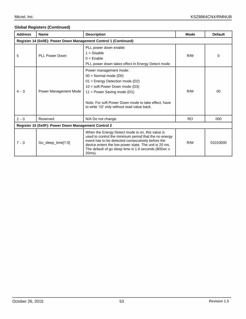
Micrel, Inc. KSZ8864CNX/RMNUB
October 26, 2015 53 Revision 1.5
Global Registers (Continued)
Address Name Description Mode Default
Register 14 (0x0E): Power Down Management Control 1 (Continued)
5 PLL Power Down
PLL power down enable: 1 = Disable 0 = Enable PLL power down takes effect in Energy Detect mode
R/W 0
4 − 3 Power Management Mode
Power management mode: 00 = Normal mode (D0) 01 = Energy Detection mode (D2) 10 = soft Power Down mode (D3) 11 = Power Saving mode (D1) Note: For soft Power Down mode to take effect, have to write ‘10’ only without read value back.
R/W 00
2 − 0 Reserved N/A Do not change. RO 000
Register 15 (0x0F): Power Down Management Control 2
7 − 0 Go_sleep_time[7:0]
When the Energy Detect mode is on, this value is used to control the minimum period that the no energy event has to be detected consecutively before the device enters the low power state. The unit is 20 ms. The default of go sleep time is 1.6 seconds (80Dec x 20ms).
R/W 01010000
Micrel, Inc. KSZ8864CNX/RMNUB
October 26, 2015 54 Revision 1.5
Port Registers The following registers are used to enable features that are assigned on a per port basis. The register bit assignments are the same for all ports, but the address for each port is different, as indicated.
Register 16 (0x10): Reserved
Register 32 (0x20): Port 1 Control 0
Register 48 (0x30): Port 2 Control 0
Register 64 (0x40): Port 3 Control 0
Register 80 (0x50): Port 4 Control 0
Address Name Description Mode Default
7 Broadcast Storm Protection Enable
1, enable broadcast storm protection for ingress packets on the port. 0, disable broadcast storm protection.
R/W 0
6 DiffServ Priority Classification Enable
1, enable DiffServ priority classification for ingress packets on port. 0, disable DiffServ function.
R/W 0
5 802.1p Priority Classification Enable
1, enable 802.1p priority classification for ingress packets on port. 0, disable 802.1p.
R/W 0
4 − 3 Port-Based Priority Classification Enable
= 00, ingress packets on port will be classified as priority 0 queue if “Diffserv” or “802.1p” classification is not enabled or fails to classify. = 01, ingress packets on port will be classified as priority 1 queue if “Diffserv” or “802.1p” classification is not enabled or fails to classify. = 10, ingress packets on port will be classified as priority 2 queue if “Diffserv” or “802.1p” classification is not enabled or fails to classify. = 11, ingress packets on port will be classified as priority 3 queue if “Diffserv” or “802.1p” classification is not enabled or fails to classify. Note: “DiffServ”, “802.1p” and port priority can be enabled at the same time. The OR’ed result of 802.1p and DSCP overwrites the port priority.
R/W 00
2 Tag insertion
1, when packets are output on the port, the switch will add 802.1q tags to packets without 802.1q tags when received. The switch will not add tags to packets already tagged. The tag inserted is the ingress port’s “port VID.” 0, disable tag insertion.
R/W 0
1 Tag Removal
1, when packets are output on the port, the switch will remove 802.1q tags from packets with 802.1q tags when received. The switch will not modify packets received without tags. 0, disable tag removal.
R/W 0
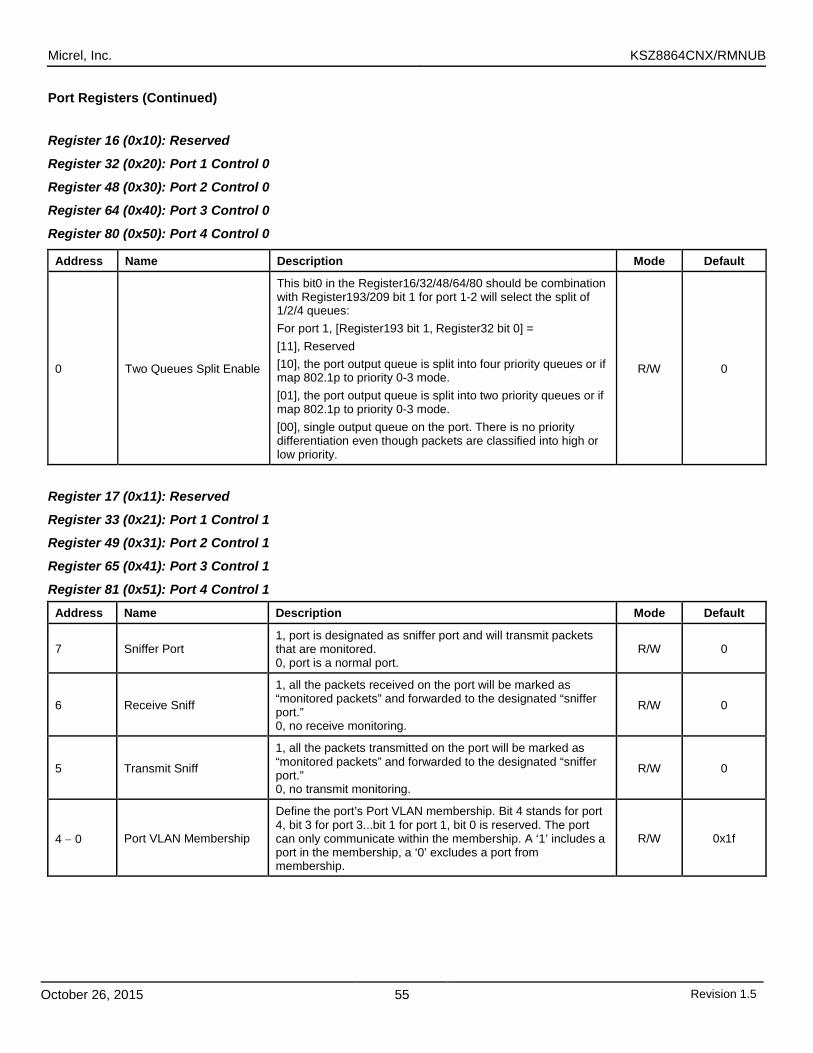
Micrel, Inc. KSZ8864CNX/RMNUB
October 26, 2015 55 Revision 1.5
Port Registers (Continued)
Register 16 (0x10): Reserved
Register 32 (0x20): Port 1 Control 0
Register 48 (0x30): Port 2 Control 0
Register 64 (0x40): Port 3 Control 0
Register 80 (0x50): Port 4 Control 0
Address Name Description Mode Default
0 Two Queues Split Enable
This bit0 in the Register16/32/48/64/80 should be combination with Register193/209 bit 1 for port 1-2 will select the split of 1/2/4 queues: For port 1, [Register193 bit 1, Register32 bit 0] = [11], Reserved [10], the port output queue is split into four priority queues or if map 802.1p to priority 0-3 mode. [01], the port output queue is split into two priority queues or if map 802.1p to priority 0-3 mode. [00], single output queue on the port. There is no priority differentiation even though packets are classified into high or low priority.
R/W 0
Register 17 (0x11): Reserved
Register 33 (0x21): Port 1 Control 1
Register 49 (0x31): Port 2 Control 1
Register 65 (0x41): Port 3 Control 1
Register 81 (0x51): Port 4 Control 1
Address Name Description Mode Default
7 Sniffer Port 1, port is designated as sniffer port and will transmit packets that are monitored. 0, port is a normal port.
R/W 0
6 Receive Sniff
1, all the packets received on the port will be marked as “monitored packets” and forwarded to the designated “sniffer port.” 0, no receive monitoring.
R/W 0
5 Transmit Sniff
1, all the packets transmitted on the port will be marked as “monitored packets” and forwarded to the designated “sniffer port.” 0, no transmit monitoring.
R/W 0
4 − 0 Port VLAN Membership
Define the port’s Port VLAN membership. Bit 4 stands for port 4, bit 3 for port 3...bit 1 for port 1, bit 0 is reserved. The port can only communicate within the membership. A ‘1’ includes a port in the membership, a ‘0’ excludes a port from membership.
R/W 0x1f
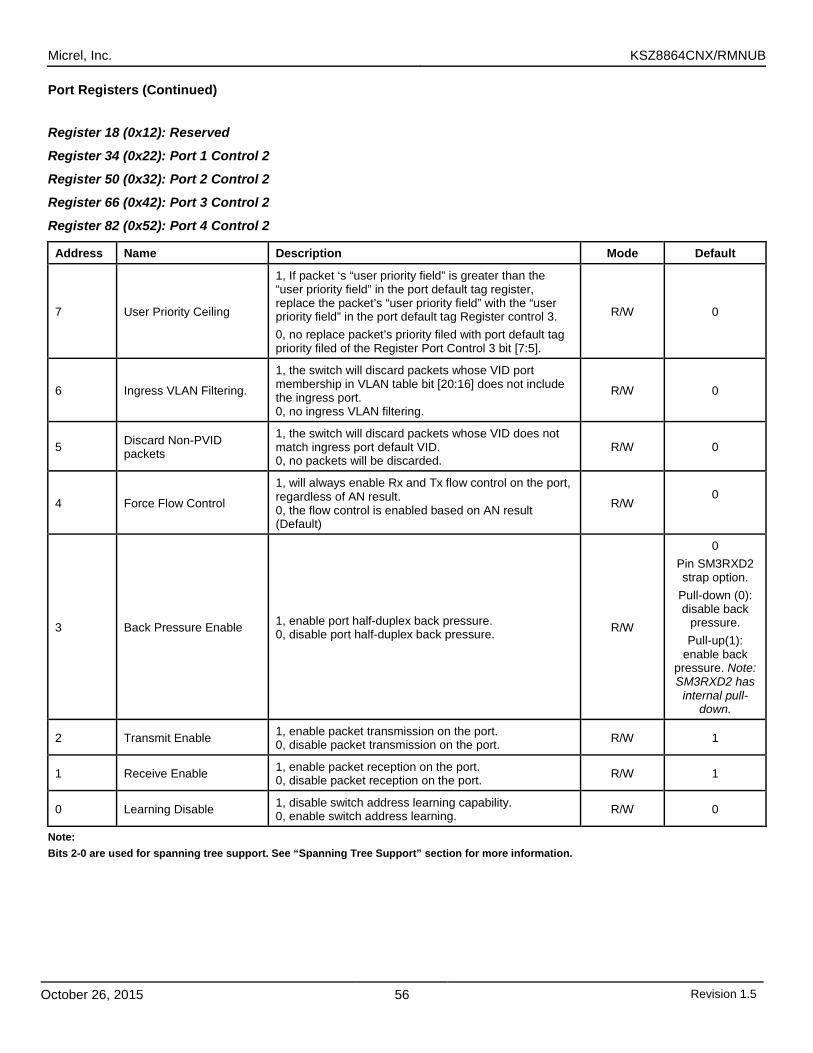
Micrel, Inc. KSZ8864CNX/RMNUB
October 26, 2015 56 Revision 1.5
Port Registers (Continued)
Register 18 (0x12): Reserved
Register 34 (0x22): Port 1 Control 2
Register 50 (0x32): Port 2 Control 2
Register 66 (0x42): Port 3 Control 2
Register 82 (0x52): Port 4 Control 2
Address Name Description Mode Default
7 User Priority Ceiling
1, If packet ‘s “user priority field” is greater than the “user priority field” in the port default tag register, replace the packet’s “user priority field” with the “user priority field” in the port default tag Register control 3. 0, no replace packet’s priority filed with port default tag priority filed of the Register Port Control 3 bit [7:5].
R/W 0
6 Ingress VLAN Filtering.
1, the switch will discard packets whose VID port membership in VLAN table bit [20:16] does not include the ingress port. 0, no ingress VLAN filtering.
R/W 0
5 Discard Non-PVID packets
1, the switch will discard packets whose VID does not match ingress port default VID. 0, no packets will be discarded.
R/W 0
4 Force Flow Control
1, will always enable Rx and Tx flow control on the port, regardless of AN result. 0, the flow control is enabled based on AN result (Default)
R/W 0
3 Back Pressure Enable 1, enable port half-duplex back pressure. 0, disable port half-duplex back pressure. R/W
0 Pin SM3RXD2 strap option.
Pull-down (0): disable back
pressure. Pull-up(1):
enable back pressure. Note: SM3RXD2 has
internal pull-down.
2 Transmit Enable 1, enable packet transmission on the port. 0, disable packet transmission on the port. R/W 1
1 Receive Enable 1, enable packet reception on the port. 0, disable packet reception on the port. R/W 1
0 Learning Disable 1, disable switch address learning capability. 0, enable switch address learning. R/W 0
Note: Bits 2-0 are used for spanning tree support. See “Spanning Tree Support” section for more information.
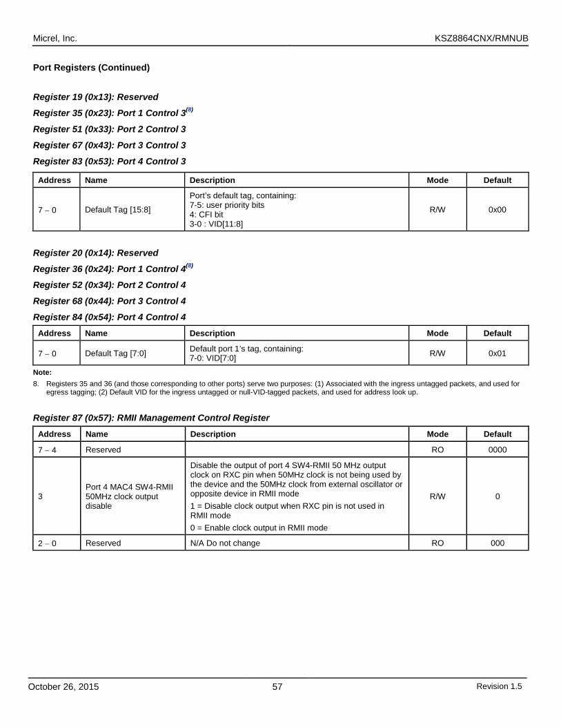
Micrel, Inc. KSZ8864CNX/RMNUB
October 26, 2015 57 Revision 1.5
Port Registers (Continued)
Register 19 (0x13): Reserved
Register 35 (0x23): Port 1 Control 3(8)
Register 51 (0x33): Port 2 Control 3
Register 67 (0x43): Port 3 Control 3
Register 83 (0x53): Port 4 Control 3
Address Name Description Mode Default
7 − 0 Default Tag [15:8]
Port’s default tag, containing: 7-5: user priority bits 4: CFI bit 3-0 : VID[11:8]
R/W 0x00
Register 20 (0x14): Reserved
Register 36 (0x24): Port 1 Control 4(8)
Register 52 (0x34): Port 2 Control 4
Register 68 (0x44): Port 3 Control 4
Register 84 (0x54): Port 4 Control 4 Address Name Description Mode Default
7 − 0 Default Tag [7:0] Default port 1’s tag, containing: 7-0: VID[7:0] R/W 0x01
Note: 8. Registers 35 and 36 (and those corresponding to other ports) serve two purposes: (1) Associated with the ingress untagged packets, and used for
egress tagging; (2) Default VID for the ingress untagged or null-VID-tagged packets, and used for address look up.
Register 87 (0x57): RMII Management Control Register
Address Name Description Mode Default
7 − 4 Reserved RO 0000
3 Port 4 MAC4 SW4-RMII 50MHz clock output disable
Disable the output of port 4 SW4-RMII 50 MHz output clock on RXC pin when 50MHz clock is not being used by the device and the 50MHz clock from external oscillator or opposite device in RMII mode 1 = Disable clock output when RXC pin is not used in RMII mode 0 = Enable clock output in RMII mode
R/W 0
2 − 0 Reserved N/A Do not change RO 000
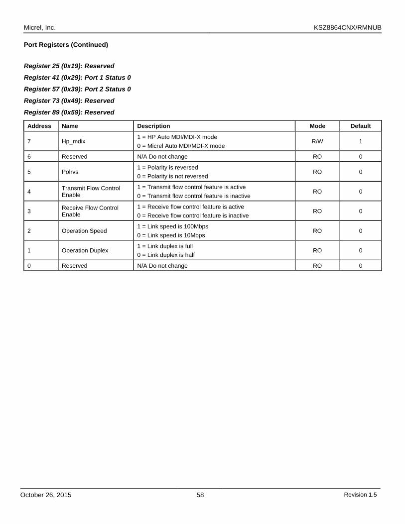
Micrel, Inc. KSZ8864CNX/RMNUB
October 26, 2015 58 Revision 1.5
Port Registers (Continued)
Register 25 (0x19): Reserved
Register 41 (0x29): Port 1 Status 0
Register 57 (0x39): Port 2 Status 0
Register 73 (0x49): Reserved
Register 89 (0x59): Reserved
Address Name Description Mode Default
7 Hp_mdix 1 = HP Auto MDI/MDI-X mode 0 = Micrel Auto MDI/MDI-X mode
R/W 1
6 Reserved N/A Do not change RO 0
5 Polrvs 1 = Polarity is reversed 0 = Polarity is not reversed
RO 0
4 Transmit Flow Control Enable
1 = Transmit flow control feature is active 0 = Transmit flow control feature is inactive
RO 0
3 Receive Flow Control Enable
1 = Receive flow control feature is active 0 = Receive flow control feature is inactive
RO 0
2 Operation Speed 1 = Link speed is 100Mbps 0 = Link speed is 10Mbps
RO 0
1 Operation Duplex 1 = Link duplex is full 0 = Link duplex is half
RO 0
0 Reserved N/A Do not change RO 0
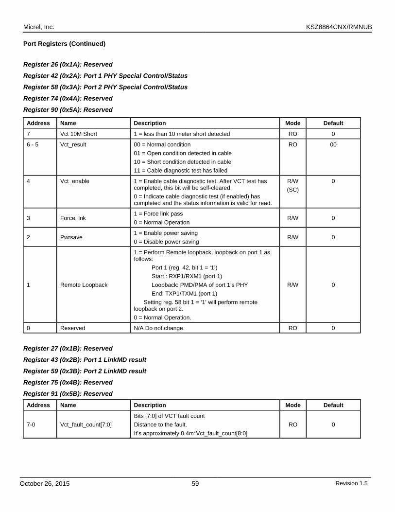
Micrel, Inc. KSZ8864CNX/RMNUB
October 26, 2015 59 Revision 1.5
Port Registers (Continued)
Register 26 (0x1A): Reserved
Register 42 (0x2A): Port 1 PHY Special Control/Status
Register 58 (0x3A): Port 2 PHY Special Control/Status
Register 74 (0x4A): Reserved
Register 90 (0x5A): Reserved
Address Name Description Mode Default
7 Vct 10M Short 1 = less than 10 meter short detected RO 0
6 - 5 Vct_result 00 = Normal condition 01 = Open condition detected in cable 10 = Short condition detected in cable 11 = Cable diagnostic test has failed
RO 00
4 Vct_enable 1 = Enable cable diagnostic test. After VCT test has completed, this bit will be self-cleared. 0 = Indicate cable diagnostic test (if enabled) has completed and the status information is valid for read.
R/W (SC)
0
3 Force_lnk 1 = Force link pass 0 = Normal Operation
R/W 0
2 Pwrsave 1 = Enable power saving 0 = Disable power saving
R/W 0
1 Remote Loopback
1 = Perform Remote loopback, loopback on port 1 as follows: Port 1 (reg. 42, bit 1 = ‘1’) Start : RXP1/RXM1 (port 1) Loopback: PMD/PMA of port 1’s PHY End: TXP1/TXM1 (port 1) Setting reg. 58 bit 1 = ‘1’ will perform remote loopback on port 2. 0 = Normal Operation.
R/W 0
0 Reserved N/A Do not change. RO 0
Register 27 (0x1B): Reserved
Register 43 (0x2B): Port 1 LinkMD result
Register 59 (0x3B): Port 2 LinkMD result
Register 75 (0x4B): Reserved
Register 91 (0x5B): Reserved
Address Name Description Mode Default
7-0 Vct_fault_count[7:0] Bits [7:0] of VCT fault count Distance to the fault. It’s approximately 0.4m*Vct_fault_count[8:0]
RO 0
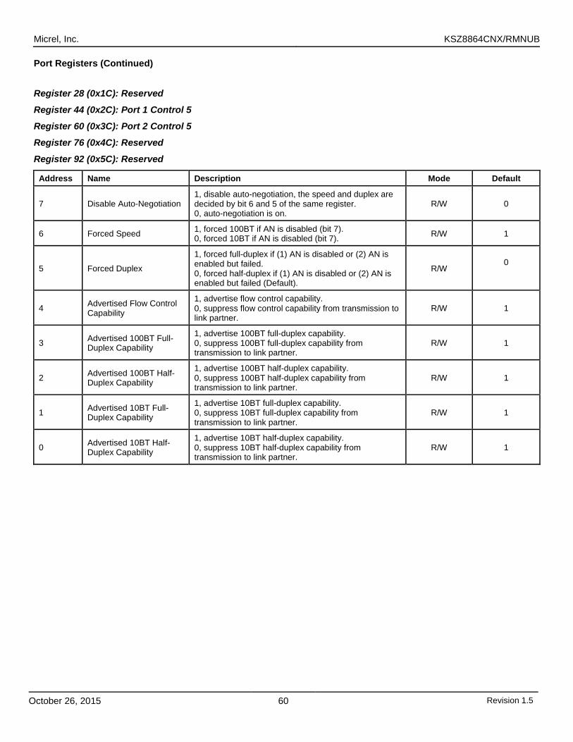
Micrel, Inc. KSZ8864CNX/RMNUB
October 26, 2015 60 Revision 1.5
Port Registers (Continued)
Register 28 (0x1C): Reserved
Register 44 (0x2C): Port 1 Control 5
Register 60 (0x3C): Port 2 Control 5
Register 76 (0x4C): Reserved
Register 92 (0x5C): Reserved
Address Name Description Mode Default
7 Disable Auto-Negotiation 1, disable auto-negotiation, the speed and duplex are decided by bit 6 and 5 of the same register. 0, auto-negotiation is on.
R/W 0
6 Forced Speed 1, forced 100BT if AN is disabled (bit 7). 0, forced 10BT if AN is disabled (bit 7). R/W 1
5 Forced Duplex
1, forced full-duplex if (1) AN is disabled or (2) AN is enabled but failed. 0, forced half-duplex if (1) AN is disabled or (2) AN is enabled but failed (Default).
R/W 0
4 Advertised Flow Control Capability
1, advertise flow control capability. 0, suppress flow control capability from transmission to link partner.
R/W 1
3 Advertised 100BT Full-Duplex Capability
1, advertise 100BT full-duplex capability. 0, suppress 100BT full-duplex capability from transmission to link partner.
R/W 1
2 Advertised 100BT Half-Duplex Capability
1, advertise 100BT half-duplex capability. 0, suppress 100BT half-duplex capability from transmission to link partner.
R/W 1
1 Advertised 10BT Full-Duplex Capability
1, advertise 10BT full-duplex capability. 0, suppress 10BT full-duplex capability from transmission to link partner.
R/W 1
0 Advertised 10BT Half-Duplex Capability
1, advertise 10BT half-duplex capability. 0, suppress 10BT half-duplex capability from transmission to link partner.
R/W 1
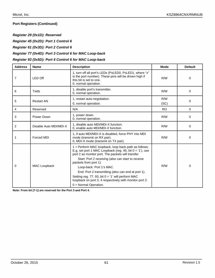
Micrel, Inc. KSZ8864CNX/RMNUB
October 26, 2015 61 Revision 1.5
Port Registers (Continued)
Register 29 (0x1D): Reserved
Register 45 (0x2D): Port 1 Control 6
Register 61 (0x3D): Port 2 Control 6
Register 77 (0x4D): Port 3 Control 6 for MAC Loop-back
Register 93 (0x5D): Port 4 Control 6 for MAC Loop-back
Address Name Description Mode Default
7 LED Off
1, turn off all port’s LEDs (PxLED0, PxLED1, where “x” is the port number). These pins will be driven high if this bit is set to one. 0, normal operation.
R/W 0
6 Txids 1, disable port’s transmitter. 0, normal operation. R/W 0
5 Restart AN 1, restart auto-negotiation. 0, normal operation.
R/W (SC)
0
4 Reserved N/A RO 0
3 Power Down 1, power down. 0, normal operation. R/W 0
2 Disable Auto MDI/MDI-X 1, disable auto MDI/MDI-X function. 0, enable auto MDI/MDI-X function. R/W 0
1 Forced MDI 1, if auto MDI/MDI-X is disabled, force PHY into MDI mode (transmit on RX pair). 0, MDI-X mode (transmit on TX pair).
R/W 0
0 MAC Loopback
1 = Perform MAC loopback, loop back path as follows: E.g. set port 1 MAC Loopback (reg. 45, bit 0 = ‘1’), use port 2 as monitor port. The packets will transfer Start: Port 2 receiving (also can start to receive packets from port 1). Loop-back: Port 1’s MAC. End: Port 2 transmitting (also can end at port 1). Setting reg. 77, 93, bit 0 = ‘1’ will perform MAC loopback on port 3, 4 respectively with monitor port 2. 0 = Normal Operation.
R/W 0
Note: From bit [7-1] are reserved for the Port 3 and Port 4.
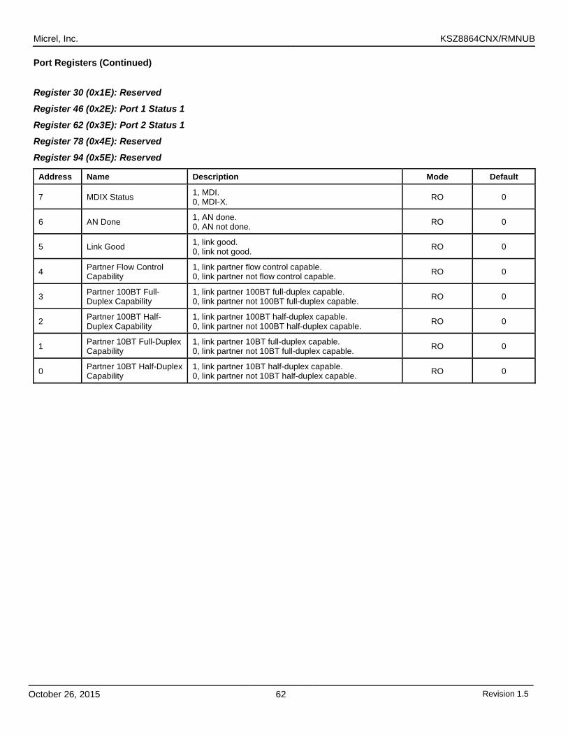
Micrel, Inc. KSZ8864CNX/RMNUB
October 26, 2015 62 Revision 1.5
Port Registers (Continued)
Register 30 (0x1E): Reserved
Register 46 (0x2E): Port 1 Status 1
Register 62 (0x3E): Port 2 Status 1
Register 78 (0x4E): Reserved
Register 94 (0x5E): Reserved
Address Name Description Mode Default
7 MDIX Status 1, MDI. 0, MDI-X. RO 0
6 AN Done 1, AN done. 0, AN not done. RO 0
5 Link Good 1, link good. 0, link not good. RO 0
4 Partner Flow Control Capability
1, link partner flow control capable. 0, link partner not flow control capable. RO 0
3 Partner 100BT Full-Duplex Capability
1, link partner 100BT full-duplex capable. 0, link partner not 100BT full-duplex capable. RO 0
2 Partner 100BT Half-Duplex Capability
1, link partner 100BT half-duplex capable. 0, link partner not 100BT half-duplex capable. RO 0
1 Partner 10BT Full-Duplex Capability
1, link partner 10BT full-duplex capable. 0, link partner not 10BT full-duplex capable. RO 0
0 Partner 10BT Half-Duplex Capability
1, link partner 10BT half-duplex capable. 0, link partner not 10BT half-duplex capable. RO 0
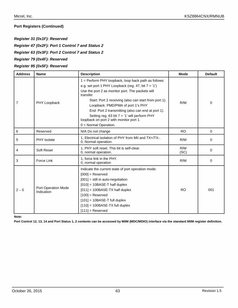
Micrel, Inc. KSZ8864CNX/RMNUB
October 26, 2015 63 Revision 1.5
Port Registers (Continued)
Register 31 (0x1F): Reserved
Register 47 (0x2F): Port 1 Control 7 and Status 2
Register 63 (0x3F): Port 2 Control 7 and Status 2
Register 79 (0x4F): Reserved
Register 95 (0x5F): Reserved
Address Name Description Mode Default
7 PHY Loopback
1 = Perform PHY loopback, loop back path as follows: e.g. set port 1 PHY Loopback (reg. 47, bit 7 = ‘1’) Use the port 2 as monitor port. The packets will transfer Start: Port 2 receiving (also can start from port 1). Loopback: PMD/PMA of port 1’s PHY End: Port 2 transmitting (also can end at port 1). Setting reg. 63 bit 7 = ‘1’ will perform PHY loopback on port 2 with monitor port 1. 0 = Normal Operation.
R/W 0
6 Reserved N/A Do not change RO 0
5 PHY Isolate 1, Electrical isolation of PHY from MII and TX+/TX-. 0, Normal operation. R/W 0
4 Soft Reset 1, PHY soft reset. This bit is self-clear. 0, normal operation.
R/W (SC) 0
3 Force Link 1, force link in the PHY. 0, normal operation R/W 0
2 − 0 Port Operation Mode Indication
Indicate the current state of port operation mode: [000] = Reserved [001] = still in auto-negotiation [010] = 10BASE-T half duplex [011] = 100BASE-TX half duplex [100] = Reserved [101] = 10BASE-T full duplex [110] = 100BASE-TX full duplex [111] = Reserved
RO 001
Note: Port Control 12, 13, 14 and Port Status 1, 2 contents can be accessed by MIIM (MDC/MDIO) interface via the standard MIIM register definition.
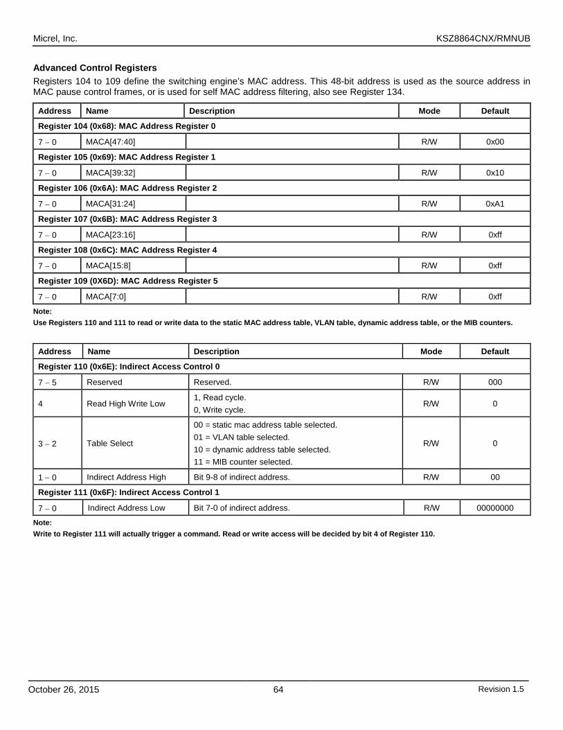
Micrel, Inc. KSZ8864CNX/RMNUB
October 26, 2015 64 Revision 1.5
Advanced Control Registers Registers 104 to 109 define the switching engine’s MAC address. This 48-bit address is used as the source address in MAC pause control frames, or is used for self MAC address filtering, also see Register 134.
Address Name Description Mode Default
Register 104 (0x68): MAC Address Register 0
7 − 0 MACA[47:40] R/W 0x00
Register 105 (0x69): MAC Address Register 1
7 − 0 MACA[39:32] R/W 0x10
Register 106 (0x6A): MAC Address Register 2
7 − 0 MACA[31:24] R/W 0xA1
Register 107 (0x6B): MAC Address Register 3
7 − 0 MACA[23:16] R/W 0xff
Register 108 (0x6C): MAC Address Register 4
7 − 0 MACA[15:8] R/W 0xff
Register 109 (0X6D): MAC Address Register 5
7 − 0 MACA[7:0] R/W 0xff
Note: Use Registers 110 and 111 to read or write data to the static MAC address table, VLAN table, dynamic address table, or the MIB counters.
Address Name Description Mode Default
Register 110 (0x6E): Indirect Access Control 0
7 − 5 Reserved Reserved. R/W 000
4 Read High Write Low 1, Read cycle. 0, Write cycle.
R/W 0
3 − 2 Table Select
00 = static mac address table selected. 01 = VLAN table selected. 10 = dynamic address table selected. 11 = MIB counter selected.
R/W 0
1 − 0 Indirect Address High Bit 9-8 of indirect address. R/W 00
Register 111 (0x6F): Indirect Access Control 1
7 − 0 Indirect Address Low Bit 7-0 of indirect address. R/W 00000000
Note: Write to Register 111 will actually trigger a command. Read or write access will be decided by bit 4 of Register 110.
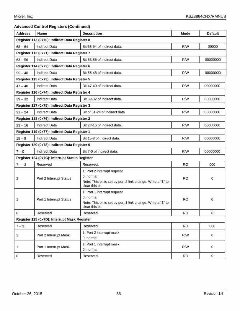
Micrel, Inc. KSZ8864CNX/RMNUB
October 26, 2015 65 Revision 1.5
Advanced Control Registers (Continued)
Address Name Description Mode Default
Register 112 (0x70): Indirect Data Register 8
68 − 64 Indirect Data Bit 68-64 of indirect data. R/W 00000
Register 113 (0x71): Indirect Data Register 7
63 − 56 Indirect Data Bit 63-56 of indirect data. R/W 00000000
Register 114 (0x72): Indirect Data Register 6
55 − 48 Indirect Data Bit 55-48 of indirect data. R/W 00000000
Register 115 (0x73): Indirect Data Register 5
47 − 40 Indirect Data Bit 47-40 of indirect data. R/W 00000000
Register 116 (0x74): Indirect Data Register 4
39 − 32 Indirect Data Bit 39-32 of indirect data. R/W 00000000
Register 117 (0x75): Indirect Data Register 3
31 − 24 Indirect Data Bit of 31-24 of indirect data R/W 00000000
Register 118 (0x76): Indirect Data Register 2
23 − 16 Indirect Data Bit 23-16 of indirect data. R/W 00000000
Register 119 (0x77): Indirect Data Register 1
15 − 8 Indirect Data Bit 15-8 of indirect data. R/W 00000000
Register 120 (0x78): Indirect Data Register 0
7 − 0 Indirect Data Bit 7-0 of indirect data. R/W 00000000
Register 124 (0x7C): Interrupt Status Register
7 − 3 Reserved Reserved. RO 000
2 Port 2 Interrupt Status
1, Port 2 interrupt request 0, normal Note: This bit is set by port 2 link change. Write a “1” to clear this bit
RO 0
1 Port 1 Interrupt Status
1, Port 1 interrupt request 0, normal Note: This bit is set by port 1 link change. Write a “1” to clear this bit
RO 0
0 Reserved Reserved. RO 0
Register 125 (0x7D): Interrupt Mask Register
7 − 3 Reserved Reserved. RO 000
2 Port 2 Interrupt Mask 1, Port 2 interrupt mask 0, normal
R/W 0
1 Port 1 Interrupt Mask 1, Port 1 interrupt mask 0, normal
R/W 0
0 Reserved Reserved. RO 0
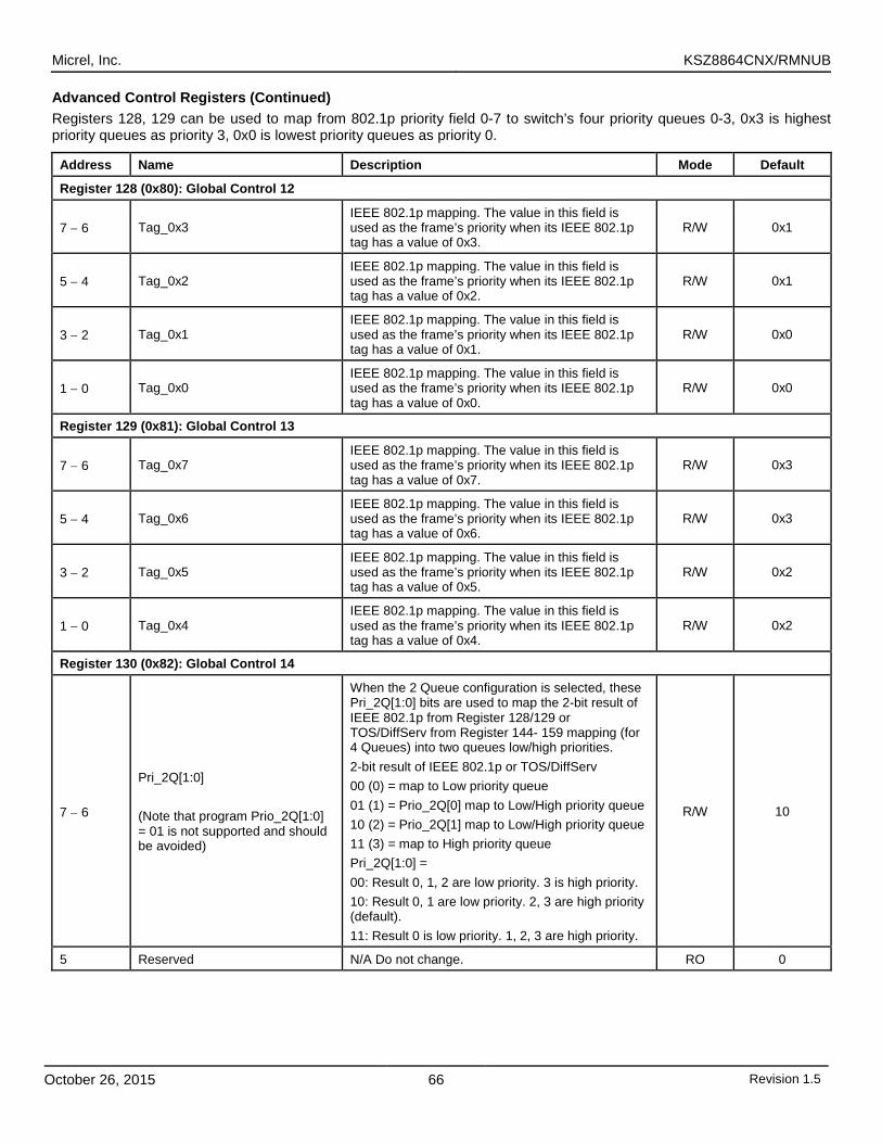
Micrel, Inc. KSZ8864CNX/RMNUB
October 26, 2015 66 Revision 1.5
Advanced Control Registers (Continued) Registers 128, 129 can be used to map from 802.1p priority field 0-7 to switch’s four priority queues 0-3, 0x3 is highest priority queues as priority 3, 0x0 is lowest priority queues as priority 0.
Address Name Description Mode Default
Register 128 (0x80): Global Control 12
7 − 6 Tag_0x3 IEEE 802.1p mapping. The value in this field is used as the frame’s priority when its IEEE 802.1p tag has a value of 0x3.
R/W 0x1
5 − 4 Tag_0x2 IEEE 802.1p mapping. The value in this field is used as the frame’s priority when its IEEE 802.1p tag has a value of 0x2.
R/W 0x1
3 − 2 Tag_0x1 IEEE 802.1p mapping. The value in this field is used as the frame’s priority when its IEEE 802.1p tag has a value of 0x1.
R/W 0x0
1 − 0 Tag_0x0 IEEE 802.1p mapping. The value in this field is used as the frame’s priority when its IEEE 802.1p tag has a value of 0x0.
R/W 0x0
Register 129 (0x81): Global Control 13
7 − 6 Tag_0x7 IEEE 802.1p mapping. The value in this field is used as the frame’s priority when its IEEE 802.1p tag has a value of 0x7.
R/W 0x3
5 − 4 Tag_0x6 IEEE 802.1p mapping. The value in this field is used as the frame’s priority when its IEEE 802.1p tag has a value of 0x6.
R/W 0x3
3 − 2 Tag_0x5 IEEE 802.1p mapping. The value in this field is used as the frame’s priority when its IEEE 802.1p tag has a value of 0x5.
R/W 0x2
1 − 0 Tag_0x4 IEEE 802.1p mapping. The value in this field is used as the frame’s priority when its IEEE 802.1p tag has a value of 0x4.
R/W 0x2
Register 130 (0x82): Global Control 14
7 − 6
Pri_2Q[1:0] (Note that program Prio_2Q[1:0] = 01 is not supported and should be avoided)
When the 2 Queue configuration is selected, these Pri_2Q[1:0] bits are used to map the 2-bit result of IEEE 802.1p from Register 128/129 or TOS/DiffServ from Register 144- 159 mapping (for 4 Queues) into two queues low/high priorities. 2-bit result of IEEE 802.1p or TOS/DiffServ 00 (0) = map to Low priority queue 01 (1) = Prio_2Q[0] map to Low/High priority queue 10 (2) = Prio_2Q[1] map to Low/High priority queue 11 (3) = map to High priority queue Pri_2Q[1:0] = 00: Result 0, 1, 2 are low priority. 3 is high priority. 10: Result 0, 1 are low priority. 2, 3 are high priority (default). 11: Result 0 is low priority. 1, 2, 3 are high priority.
R/W 10
5 Reserved N/A Do not change. RO 0
Micrel, Inc. KSZ8864CNX/RMNUB
October 26, 2015 67 Revision 1.5
Advanced Control Registers (Continued)
Address Name Description Mode Default
Register 130 (0x82): Global Control 14
4 Reserved N/A Do not change. RO 0
3 − 2 Reserved N/A Do not change. RO 01
1 Reserved N/A Do not change. RO 0
0 Reserved N/A Do not change. RO 0.
Register 131 (0x83): Global Control 15
7 Reserved N/A RO 0
6 Reserved N/A RO 0
5 Unknown unicast packet forward 1 = enable supporting unknown unicast packet forward 0 = disable
R/W 0
4 − 0 Unknown unicast packet forward port map
00000 = filter unknown unicast packet 00001 = reserved 0001x = forward unknown unicast packet to Port 1 0010x = forward unknown unicast packet to Port 2 0011x = forward unknown unicast packet to Port 1, Port 2 1111x = broadcast unknown unicast packet to all ports Note: x = ‘0’ or ‘1’, bit 0 is reserved.
R/W 00000
Register 132 (0x84): Global Control 16
7 − 6 Chip I/O output drive strength select[1:0]
Output drive strength select[1:0] = 00 = 4mA drive strength 01 = 8mA drive strength (default) 10 = 10mA drive strength 11 = 14mA drive strength
R/W 01
5 Unknown multicast packet forward (not including IP multicast packet)
1 = enable supporting unknown multicast packet forward 0 = disable
R/W 0
4 − 0 Unknown multicast packet forward port map
00000 = filter unknown multicast packet 00001 = reserved 0001x = forward unknown unicast packet to Port 1 0010x = forward unknown unicast packet to Port 2 0011x = forward unknown unicast packet to Port 1, Port 2 1111x = broadcast unknown unicast packet to all ports Note: x = ‘0’ or ‘1’, bit 0 is reserved.
R/W 00000
Micrel, Inc. KSZ8864CNX/RMNUB
October 26, 2015 68 Revision 1.5
Advanced Control Registers (Continued)
Address Name Description Mode Default
Register 133(0x85): Global Control 17
7 − 6 Reserved RO 00
5 Unknown VID packet forward 1 = enable supporting unknown VID packet forward 0 = disable
R/W 0
4 − 0 Unknown VID packet forward port map
00000 = filter unknown VID packet 00001 = reserved 0001x = forward unknown unicast packet to Port 1 0010x = forward unknown unicast packet to Port 2 0011x = forward unknown unicast packet to Port 1, Port 2 1111x = broadcast unknown unicast packet to all ports Note: x = ‘0’ or ‘1’, bit 0 is reserved.
R/W 00000
Register 134 (0x86): Global Control 18
7 Reserved N/A RO 0
6 Self-Address Filter Enable
1 = Enable filtering of self-address unicast and multicast packet 0 = Do not filter self-address packet Note: The self-address filtering will filter packets on the egress port, self MAC address is assigned in the Register 104-109.
R/W 0
5 Unknown IP multicast packet forward
1 = enable supporting unknown IP multicast packet forward 0 = disable
R/W 0
4 − 0 Unknown IP multicast packet forward port map
00000 = filter unknown IP multicast packet 00001 = reserved 0001x = forward unknown unicast packet to Port 1 0010x = forward unknown unicast packet to Port 2 0011x = forward unknown unicast packet to Port 1, Port 2 1111x = broadcast unknown unicast packet to all ports Note: x = ‘0’ or ‘1’, bit 0 is reserved.
R/W 00000
Micrel, Inc. KSZ8864CNX/RMNUB
October 26, 2015 69 Revision 1.5
Advanced Control Registers (Continued)
Address Name Description Mode Default
Register 135 (0x87): Global Control 19
7 Reserved N/A Do not change. RO 0
6 Reserved N/A Do not change. RO 0
5 − 4 Ingress Rate Limit Period
The unit period for calculating Ingress Rate Limit 00 = 16 ms 01 = 64 ms 1x = 256 ms
R/W 01
3 Queue-based Egress Rate Limit Enabled
Enable Queue-based Egress Rate Limit 0 = port-base Egress Rate Limit (default) 1 = queue-based Egress Rate Limit
R/W 0
2 Insertion Source Port PVID Tag Selection Enable
1 = enable source port PVID tag insertion or non-insertion option on the egress port for each source port PVID based on the ports Registers control 8. 0 = disable, all packets from any ingress port will be inserted PVID based on Register Port Control 0 bit 2.
R/W 0
1 − 0 Reserved N/A Do not change. RO 00
Register 144 (0x90): TOS Priority Control Register 0 The IPv4/IPv6 TOS priority control registers implement a fully decoded 64 bit differentiated services code point (DSCP) register used to determine priority from the 6 bit TOS field in the IP header. The most significant 6 bits of the TOS field are fully decoded into 64 possibilities, and the singular code that results is mapped to the value in the corresponding bit in the DSCP register.
7 − 6 DSCP[7:6]
IPv4 and IPv6 mapping The value in this field is used as the frame’s priority when bits [7:2] of the frame’s IP TOS/DiffServ/Traffic Class value are 0x03.
R/W 00
5 − 4 DSCP[5:4]
IPv4 and IPv6 mapping The value in this field is used as the frame’s priority when bits [7:2] of the frame’s IP TOS/DiffServ/Traffic Class value is 0x02
R/W 00
3 − 2 DSCP[3:2]
IPv4 and IPv6 mapping The value in this field is used as the frame’s priority when bits [7:2] of the frame’s IP TOS/DiffServ/Traffic Class value is 0x01
R/W 00
1 - 0 DSCP[1:0]
IPv4 and IPv6 mapping The value in this field is used as the frame’s priority when bits [7:2] of the frame’s IP TOS/DiffServ/Traffic Class value is 0x00
R/W 00
Micrel, Inc. KSZ8864CNX/RMNUB
October 26, 2015 70 Revision 1.5
Advanced Control Registers (Continued)
Address Name Description Mode Default
Register 145 (0x91): TOS Priority Control Register 1
7 − 6 DSCP[15:14] IPv4 and IPv6 mapping _ for value 0x07 R/W 00
5 − 4 DSCP[13:12] IPv4 and IPv6 mapping _ for value 0x06 R/W 00
3 − 2 DSCP[11:10] IPv4 and IPv6 mapping _ for value 0x05 R/W 00
1 − 0 DSCP[9:8] IPv4 and IPv6 mapping _ for value 0x04 R/W 00
Register 146 (0x92): TOS Priority Control Register 2
7 − 6 DSCP[23:22] IPv4 and IPv6 mapping _ for value 0x0B R/W 00
5 − 4 DSCP[21:20] IPv4 and IPv6 mapping _ for value 0x0A R/W 00
3 − 2 DSCP[19:18] IPv4 and IPv6 mapping _ for value 0x09 R/W 00
1 − 0 DSCP[17:16] IPv4 and IPv6 mapping _ for value 0x08 R/W 00
Register 147 (0x93): TOS Priority Control Register 3
7 − 6 DSCP[31:30] IPv4 and IPv6 mapping _ for value 0x0F R/W 00
5 −4 DSCP[29:28] IPv4 and IPv6 mapping _ for value 0x0E R/W 00
3 −2 DSCP[27:26] IPv4 and IPv6 mapping _ for value 0x0D R/W 00
1 −0 DSCP[25:24] IPv4 and IPv6 mapping _ for value 0x0C R/W 00
Register 148 (0x94): TOS Priority Control Register 4
7 −6 DSCP[39:38] IPv4 and IPv6 mapping _ for value 0x13 R/W 00
5 −4 DSCP[37:36] IPv4 and IPv6 mapping _ for value 0x12 R/W 00
3 −2 DSCP[35:34] IPv4 and IPv6 mapping _ for value 0x11 R/W 00
1 −0 DSCP[33:32] IPv4 and IPv6 mapping _ for value 0x10 R/W 00
Register 149 (0x95): TOS Priority Control Register 5
7 −6 DSCP[47:46] IPv4 and IPv6 mapping _ for value 0x17 R/W 00
5 −4 DSCP[45:44] IPv4 and IPv6 mapping _ for value 0x16 R/W 00
3 −2 DSCP[43:42] IPv4 and IPv6 mapping _ for value 0x15 R/W 00
1 −0 DSCP[41:40] IPv4 and IPv6 mapping _ for value 0x14 R/W 00
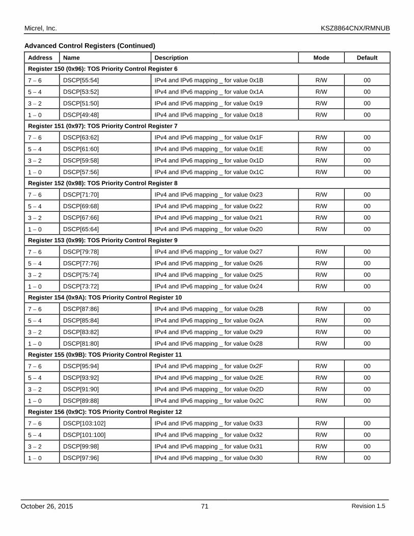
Micrel, Inc. KSZ8864CNX/RMNUB
October 26, 2015 71 Revision 1.5
Advanced Control Registers (Continued)
Address Name Description Mode Default
Register 150 (0x96): TOS Priority Control Register 6
7 − 6 DSCP[55:54] IPv4 and IPv6 mapping _ for value 0x1B R/W 00
5 − 4 DSCP[53:52] IPv4 and IPv6 mapping _ for value 0x1A R/W 00
3 − 2 DSCP[51:50] IPv4 and IPv6 mapping _ for value 0x19 R/W 00
1 − 0 DSCP[49:48] IPv4 and IPv6 mapping _ for value 0x18 R/W 00
Register 151 (0x97): TOS Priority Control Register 7
7 − 6 DSCP[63:62] IPv4 and IPv6 mapping _ for value 0x1F R/W 00
5 − 4 DSCP[61:60] IPv4 and IPv6 mapping _ for value 0x1E R/W 00
3 − 2 DSCP[59:58] IPv4 and IPv6 mapping _ for value 0x1D R/W 00
1 − 0 DSCP[57:56] IPv4 and IPv6 mapping _ for value 0x1C R/W 00
Register 152 (0x98): TOS Priority Control Register 8
7 − 6 DSCP[71:70] IPv4 and IPv6 mapping _ for value 0x23 R/W 00
5 − 4 DSCP[69:68] IPv4 and IPv6 mapping _ for value 0x22 R/W 00
3 − 2 DSCP[67:66] IPv4 and IPv6 mapping _ for value 0x21 R/W 00
1 − 0 DSCP[65:64] IPv4 and IPv6 mapping _ for value 0x20 R/W 00
Register 153 (0x99): TOS Priority Control Register 9
7 − 6 DSCP[79:78] IPv4 and IPv6 mapping _ for value 0x27 R/W 00
5 − 4 DSCP[77:76] IPv4 and IPv6 mapping _ for value 0x26 R/W 00
3 − 2 DSCP[75:74] IPv4 and IPv6 mapping _ for value 0x25 R/W 00
1 − 0 DSCP[73:72] IPv4 and IPv6 mapping _ for value 0x24 R/W 00
Register 154 (0x9A): TOS Priority Control Register 10
7 − 6 DSCP[87:86] IPv4 and IPv6 mapping _ for value 0x2B R/W 00
5 − 4 DSCP[85:84] IPv4 and IPv6 mapping _ for value 0x2A R/W 00
3 − 2 DSCP[83:82] IPv4 and IPv6 mapping _ for value 0x29 R/W 00
1 − 0 DSCP[81:80] IPv4 and IPv6 mapping _ for value 0x28 R/W 00
Register 155 (0x9B): TOS Priority Control Register 11
7 − 6 DSCP[95:94] IPv4 and IPv6 mapping _ for value 0x2F R/W 00
5 − 4 DSCP[93:92] IPv4 and IPv6 mapping _ for value 0x2E R/W 00
3 − 2 DSCP[91:90] IPv4 and IPv6 mapping _ for value 0x2D R/W 00
1 − 0 DSCP[89:88] IPv4 and IPv6 mapping _ for value 0x2C R/W 00
Register 156 (0x9C): TOS Priority Control Register 12
7 − 6 DSCP[103:102] IPv4 and IPv6 mapping _ for value 0x33 R/W 00
5 − 4 DSCP[101:100] IPv4 and IPv6 mapping _ for value 0x32 R/W 00
3 − 2 DSCP[99:98] IPv4 and IPv6 mapping _ for value 0x31 R/W 00
1 − 0 DSCP[97:96] IPv4 and IPv6 mapping _ for value 0x30 R/W 00
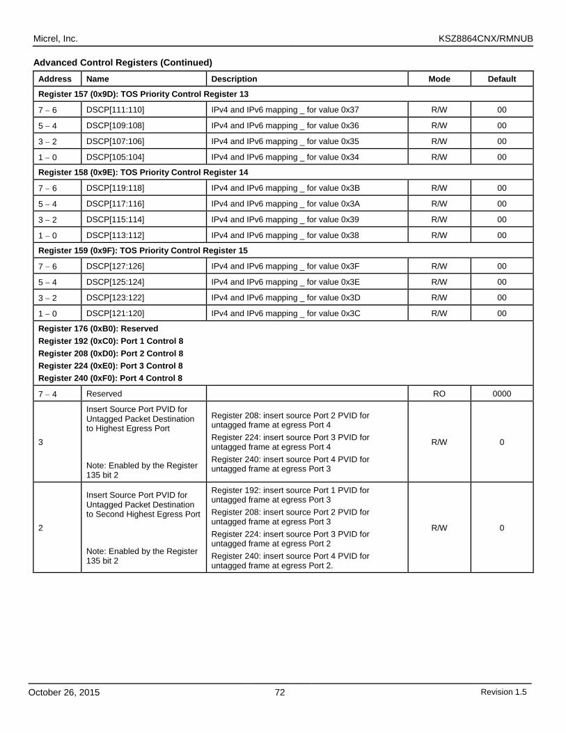
Micrel, Inc. KSZ8864CNX/RMNUB
October 26, 2015 72 Revision 1.5
Advanced Control Registers (Continued)
Address Name Description Mode Default
Register 157 (0x9D): TOS Priority Control Register 13
7 − 6 DSCP[111:110] IPv4 and IPv6 mapping _ for value 0x37 R/W 00
5 − 4 DSCP[109:108] IPv4 and IPv6 mapping _ for value 0x36 R/W 00
3 − 2 DSCP[107:106] IPv4 and IPv6 mapping _ for value 0x35 R/W 00
1 − 0 DSCP[105:104] IPv4 and IPv6 mapping _ for value 0x34 R/W 00
Register 158 (0x9E): TOS Priority Control Register 14
7 − 6 DSCP[119:118] IPv4 and IPv6 mapping _ for value 0x3B R/W 00
5 − 4 DSCP[117:116] IPv4 and IPv6 mapping _ for value 0x3A R/W 00
3 − 2 DSCP[115:114] IPv4 and IPv6 mapping _ for value 0x39 R/W 00
1 − 0 DSCP[113:112] IPv4 and IPv6 mapping _ for value 0x38 R/W 00
Register 159 (0x9F): TOS Priority Control Register 15
7 − 6 DSCP[127:126] IPv4 and IPv6 mapping _ for value 0x3F R/W 00
5 − 4 DSCP[125:124] IPv4 and IPv6 mapping _ for value 0x3E R/W 00
3 − 2 DSCP[123:122] IPv4 and IPv6 mapping _ for value 0x3D R/W 00
1 − 0 DSCP[121:120] IPv4 and IPv6 mapping _ for value 0x3C R/W 00
Register 176 (0xB0): Reserved Register 192 (0xC0): Port 1 Control 8 Register 208 (0xD0): Port 2 Control 8 Register 224 (0xE0): Port 3 Control 8 Register 240 (0xF0): Port 4 Control 8
7 − 4 Reserved RO 0000
3
Insert Source Port PVID for Untagged Packet Destination to Highest Egress Port Note: Enabled by the Register 135 bit 2
Register 208: insert source Port 2 PVID for untagged frame at egress Port 4 Register 224: insert source Port 3 PVID for untagged frame at egress Port 4 Register 240: insert source Port 4 PVID for untagged frame at egress Port 3
R/W 0
2
Insert Source Port PVID for Untagged Packet Destination to Second Highest Egress Port Note: Enabled by the Register 135 bit 2
Register 192: insert source Port 1 PVID for untagged frame at egress Port 3 Register 208: insert source Port 2 PVID for untagged frame at egress Port 3 Register 224: insert source Port 3 PVID for untagged frame at egress Port 2 Register 240: insert source Port 4 PVID for untagged frame at egress Port 2.
R/W 0
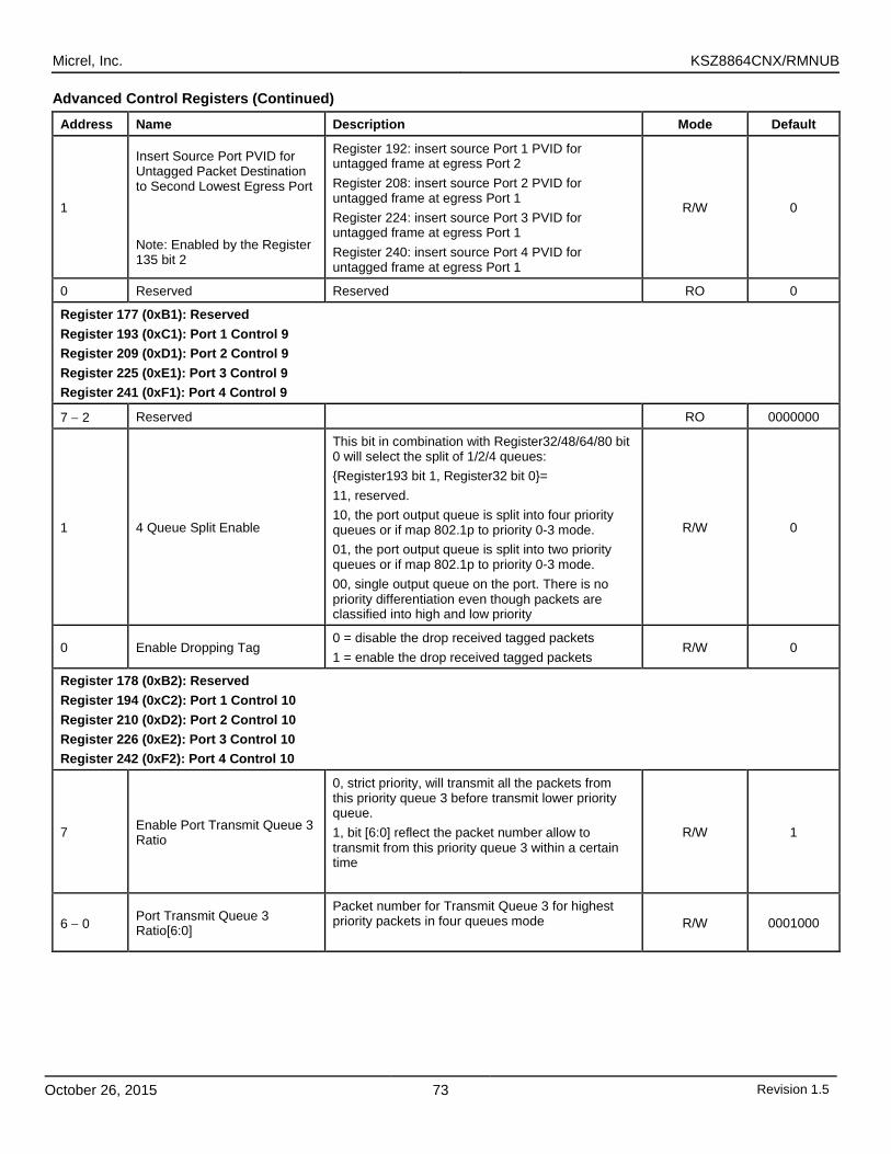
Micrel, Inc. KSZ8864CNX/RMNUB
October 26, 2015 73 Revision 1.5
Advanced Control Registers (Continued)
Address Name Description Mode Default
1
Insert Source Port PVID for Untagged Packet Destination to Second Lowest Egress Port Note: Enabled by the Register 135 bit 2
Register 192: insert source Port 1 PVID for untagged frame at egress Port 2 Register 208: insert source Port 2 PVID for untagged frame at egress Port 1 Register 224: insert source Port 3 PVID for untagged frame at egress Port 1 Register 240: insert source Port 4 PVID for untagged frame at egress Port 1
R/W 0
0 Reserved Reserved RO 0
Register 177 (0xB1): Reserved Register 193 (0xC1): Port 1 Control 9 Register 209 (0xD1): Port 2 Control 9 Register 225 (0xE1): Port 3 Control 9 Register 241 (0xF1): Port 4 Control 9
7 − 2 Reserved RO 0000000
1 4 Queue Split Enable
This bit in combination with Register32/48/64/80 bit 0 will select the split of 1/2/4 queues: Register193 bit 1, Register32 bit 0= 11, reserved. 10, the port output queue is split into four priority queues or if map 802.1p to priority 0-3 mode. 01, the port output queue is split into two priority queues or if map 802.1p to priority 0-3 mode. 00, single output queue on the port. There is no priority differentiation even though packets are classified into high and low priority
R/W 0
0 Enable Dropping Tag 0 = disable the drop received tagged packets 1 = enable the drop received tagged packets
R/W 0
Register 178 (0xB2): Reserved Register 194 (0xC2): Port 1 Control 10 Register 210 (0xD2): Port 2 Control 10 Register 226 (0xE2): Port 3 Control 10 Register 242 (0xF2): Port 4 Control 10
7 Enable Port Transmit Queue 3 Ratio
0, strict priority, will transmit all the packets from this priority queue 3 before transmit lower priority queue. 1, bit [6:0] reflect the packet number allow to transmit from this priority queue 3 within a certain time
R/W 1
6 − 0 Port Transmit Queue 3 Ratio[6:0]
Packet number for Transmit Queue 3 for highest priority packets in four queues mode
R/W 0001000
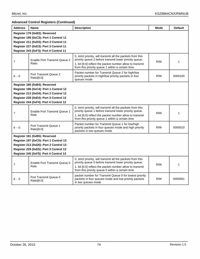
Micrel, Inc. KSZ8864CNX/RMNUB
October 26, 2015 74 Revision 1.5
Advanced Control Registers (Continued)
Address Name Description Mode Default
Register 179 (0xB3): Reserved Register 195 (0xC3): Port 1 Control 11 Register 211 (0xD3): Port 2 Control 11 Register 227 (0xE3): Port 3 Control 11 Register 243 (0xF3): Port 4 Control 11
7 Enable Port Transmit Queue 2 Ratio
0, strict priority, will transmit all the packets from this priority queue 2 before transmit lower priority queue. 1, bit [6:0] reflect the packet number allow to transmit from this priority queue 1 within a certain time
R/W 1
6 − 0 Port Transmit Queue 2 Ratio[6:0]
Packet number for Transmit Queue 2 for high/low priority packets in high/low priority packets in four queues mode
R/W 0000100
Register 180 (0xB4): Reserved Register 196 (0xC4): Port 1 Control 12 Register 212 (0xD4): Port 2 Control 12 Register 228 (0xE4): Port 3 Control 12 Register 244 (0xF4): Port 4 Control 12
7 Enable Port Transmit Queue 1 Rate
0, strict priority, will transmit all the packets from this priority queue 1 before transmit lower priority queue. 1, bit [6:0] reflect the packet number allow to transmit from this priority queue 1 within a certain time
R/W 1
6 − 0 Port Transmit Queue 1 Ratio[6:0]
Packet number for Transmit Queue 1 for low/high priority packets in four queues mode and high priority packets in two queues mode
R/W 0000010
Register 181 (0xB5): Reserved Register 197 (0xC5): Port 1 Control 13 Register 213 (0xD5): Port 2 Control 13 Register 229 (0xE5): Port 3 Control 13 Register 245 (0xF5): Port 4 Control 13
7 Enable Port Transmit Queue 0 Rate
0, strict priority, will transmit all the packets from this priority queue 0 before transmit lower priority queue. 1, bit [6:0] reflect the packet number allow to transmit from this priority queue 0 within a certain time
R/W 1
6 − 0 Port Transmit Queue 0 Ratio[6:0]
packet number for Transmit Queue 0 for lowest priority packets in four queues mode and low priority packets in two queues mode
R/W 0000001
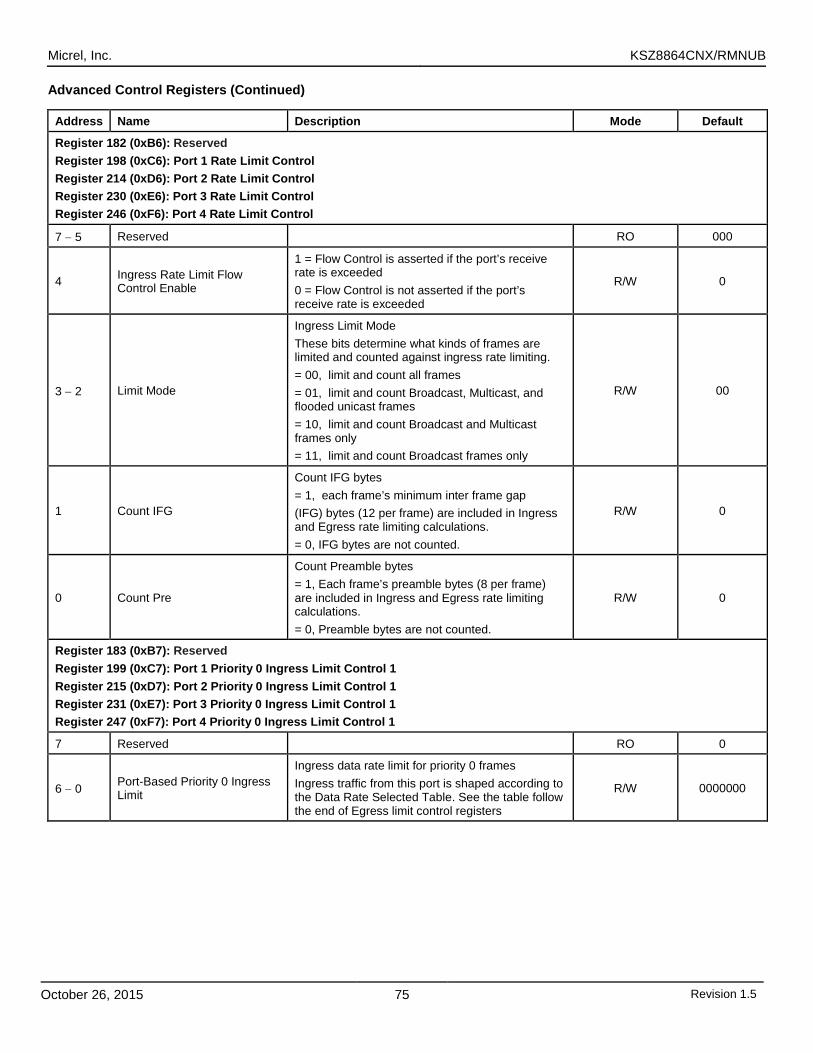
Micrel, Inc. KSZ8864CNX/RMNUB
October 26, 2015 75 Revision 1.5
Advanced Control Registers (Continued)
Address Name Description Mode Default
Register 182 (0xB6): Reserved Register 198 (0xC6): Port 1 Rate Limit Control Register 214 (0xD6): Port 2 Rate Limit Control Register 230 (0xE6): Port 3 Rate Limit Control Register 246 (0xF6): Port 4 Rate Limit Control
7 − 5 Reserved RO 000
4 Ingress Rate Limit Flow Control Enable
1 = Flow Control is asserted if the port’s receive rate is exceeded 0 = Flow Control is not asserted if the port’s receive rate is exceeded
R/W 0
3 − 2 Limit Mode
Ingress Limit Mode These bits determine what kinds of frames are limited and counted against ingress rate limiting. = 00, limit and count all frames = 01, limit and count Broadcast, Multicast, and flooded unicast frames = 10, limit and count Broadcast and Multicast frames only = 11, limit and count Broadcast frames only
R/W 00
1 Count IFG
Count IFG bytes = 1, each frame’s minimum inter frame gap (IFG) bytes (12 per frame) are included in Ingress and Egress rate limiting calculations. = 0, IFG bytes are not counted.
R/W 0
0 Count Pre
Count Preamble bytes = 1, Each frame’s preamble bytes (8 per frame) are included in Ingress and Egress rate limiting calculations. = 0, Preamble bytes are not counted.
R/W 0
Register 183 (0xB7): Reserved Register 199 (0xC7): Port 1 Priority 0 Ingress Limit Control 1 Register 215 (0xD7): Port 2 Priority 0 Ingress Limit Control 1 Register 231 (0xE7): Port 3 Priority 0 Ingress Limit Control 1 Register 247 (0xF7): Port 4 Priority 0 Ingress Limit Control 1
7 Reserved RO 0
6 − 0 Port-Based Priority 0 Ingress Limit
Ingress data rate limit for priority 0 frames Ingress traffic from this port is shaped according to the Data Rate Selected Table. See the table follow the end of Egress limit control registers
R/W 0000000
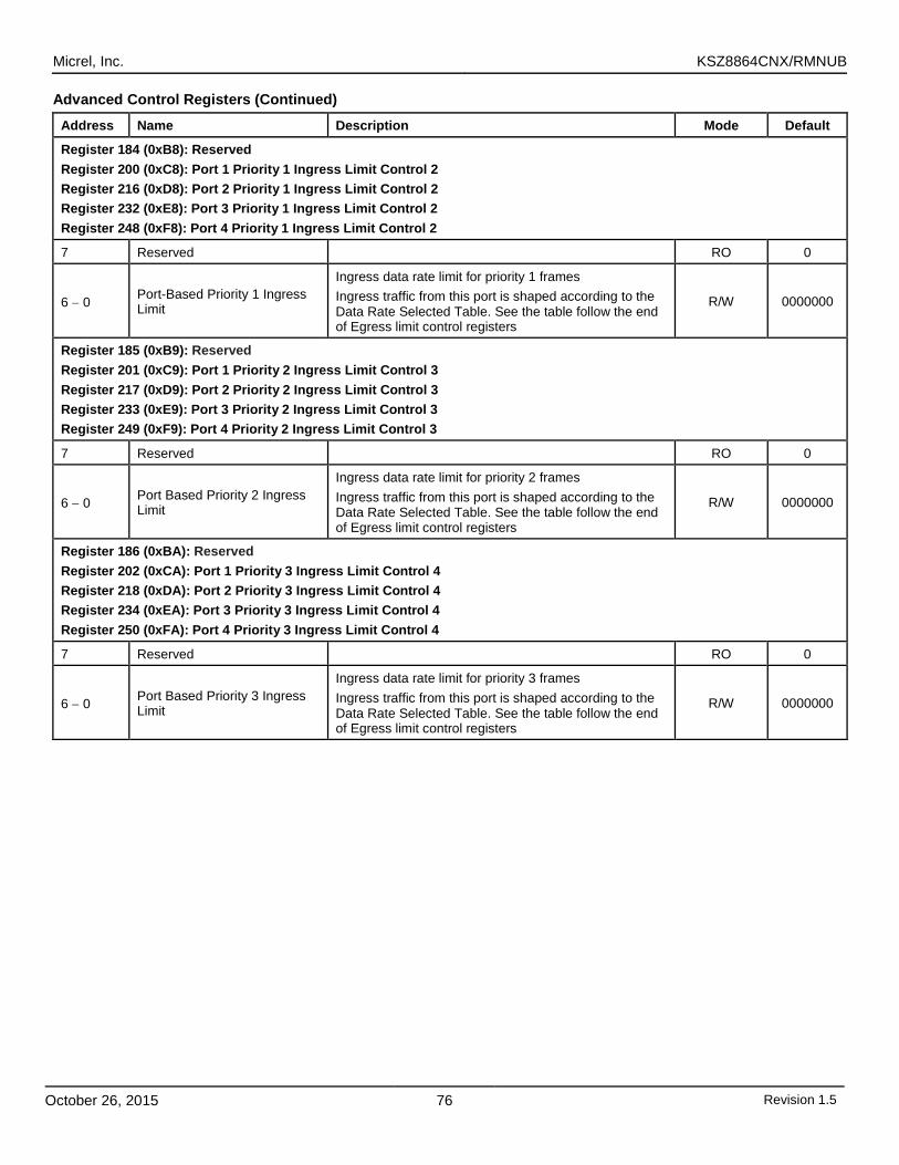
Micrel, Inc. KSZ8864CNX/RMNUB
October 26, 2015 76 Revision 1.5
Advanced Control Registers (Continued)
Address Name Description Mode Default
Register 184 (0xB8): Reserved Register 200 (0xC8): Port 1 Priority 1 Ingress Limit Control 2 Register 216 (0xD8): Port 2 Priority 1 Ingress Limit Control 2 Register 232 (0xE8): Port 3 Priority 1 Ingress Limit Control 2 Register 248 (0xF8): Port 4 Priority 1 Ingress Limit Control 2
7 Reserved RO 0
6 − 0 Port-Based Priority 1 Ingress Limit
Ingress data rate limit for priority 1 frames Ingress traffic from this port is shaped according to the Data Rate Selected Table. See the table follow the end of Egress limit control registers
R/W 0000000
Register 185 (0xB9): Reserved Register 201 (0xC9): Port 1 Priority 2 Ingress Limit Control 3 Register 217 (0xD9): Port 2 Priority 2 Ingress Limit Control 3 Register 233 (0xE9): Port 3 Priority 2 Ingress Limit Control 3 Register 249 (0xF9): Port 4 Priority 2 Ingress Limit Control 3
7 Reserved RO 0
6 − 0 Port Based Priority 2 Ingress Limit
Ingress data rate limit for priority 2 frames Ingress traffic from this port is shaped according to the Data Rate Selected Table. See the table follow the end of Egress limit control registers
R/W 0000000
Register 186 (0xBA): Reserved Register 202 (0xCA): Port 1 Priority 3 Ingress Limit Control 4 Register 218 (0xDA): Port 2 Priority 3 Ingress Limit Control 4 Register 234 (0xEA): Port 3 Priority 3 Ingress Limit Control 4 Register 250 (0xFA): Port 4 Priority 3 Ingress Limit Control 4
7 Reserved RO 0
6 − 0 Port Based Priority 3 Ingress Limit
Ingress data rate limit for priority 3 frames Ingress traffic from this port is shaped according to the Data Rate Selected Table. See the table follow the end of Egress limit control registers
R/W 0000000
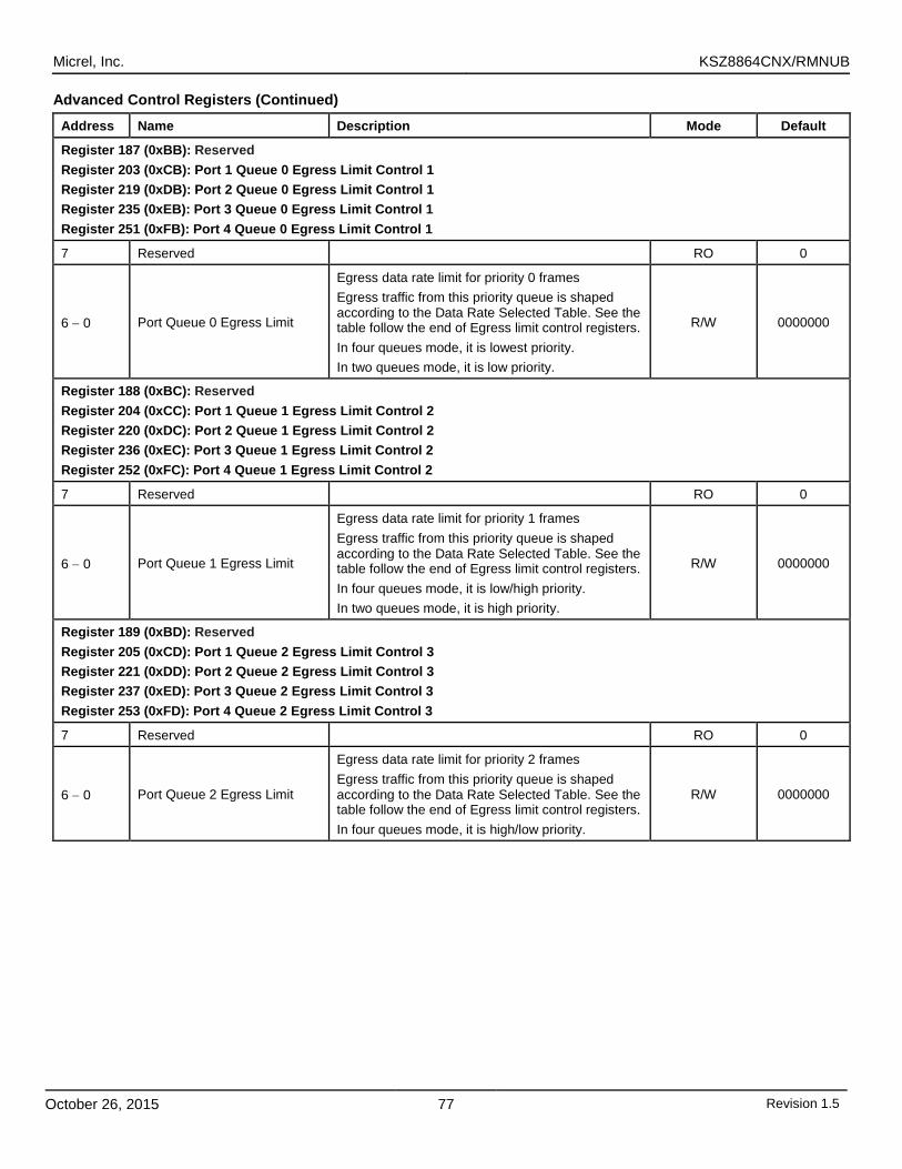
Micrel, Inc. KSZ8864CNX/RMNUB
October 26, 2015 77 Revision 1.5
Advanced Control Registers (Continued)
Address Name Description Mode Default
Register 187 (0xBB): Reserved Register 203 (0xCB): Port 1 Queue 0 Egress Limit Control 1 Register 219 (0xDB): Port 2 Queue 0 Egress Limit Control 1 Register 235 (0xEB): Port 3 Queue 0 Egress Limit Control 1 Register 251 (0xFB): Port 4 Queue 0 Egress Limit Control 1
7 Reserved RO 0
6 − 0 Port Queue 0 Egress Limit
Egress data rate limit for priority 0 frames Egress traffic from this priority queue is shaped according to the Data Rate Selected Table. See the table follow the end of Egress limit control registers. In four queues mode, it is lowest priority. In two queues mode, it is low priority.
R/W 0000000
Register 188 (0xBC): Reserved Register 204 (0xCC): Port 1 Queue 1 Egress Limit Control 2 Register 220 (0xDC): Port 2 Queue 1 Egress Limit Control 2 Register 236 (0xEC): Port 3 Queue 1 Egress Limit Control 2 Register 252 (0xFC): Port 4 Queue 1 Egress Limit Control 2
7 Reserved RO 0
6 − 0 Port Queue 1 Egress Limit
Egress data rate limit for priority 1 frames Egress traffic from this priority queue is shaped according to the Data Rate Selected Table. See the table follow the end of Egress limit control registers. In four queues mode, it is low/high priority. In two queues mode, it is high priority.
R/W 0000000
Register 189 (0xBD): Reserved Register 205 (0xCD): Port 1 Queue 2 Egress Limit Control 3 Register 221 (0xDD): Port 2 Queue 2 Egress Limit Control 3 Register 237 (0xED): Port 3 Queue 2 Egress Limit Control 3 Register 253 (0xFD): Port 4 Queue 2 Egress Limit Control 3
7 Reserved RO 0
6 − 0 Port Queue 2 Egress Limit
Egress data rate limit for priority 2 frames Egress traffic from this priority queue is shaped according to the Data Rate Selected Table. See the table follow the end of Egress limit control registers. In four queues mode, it is high/low priority.
R/W 0000000
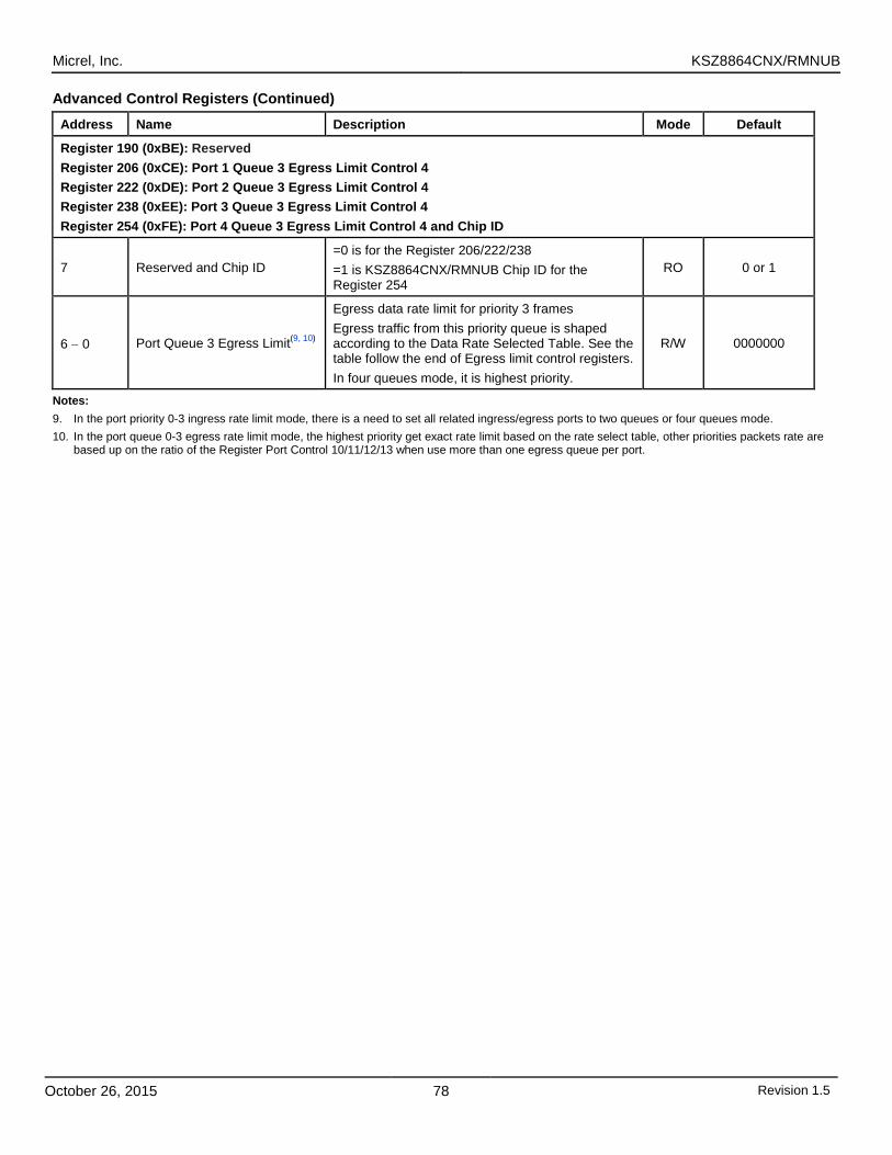
Micrel, Inc. KSZ8864CNX/RMNUB
October 26, 2015 78 Revision 1.5
Advanced Control Registers (Continued)
Address Name Description Mode Default
Register 190 (0xBE): Reserved Register 206 (0xCE): Port 1 Queue 3 Egress Limit Control 4 Register 222 (0xDE): Port 2 Queue 3 Egress Limit Control 4 Register 238 (0xEE): Port 3 Queue 3 Egress Limit Control 4 Register 254 (0xFE): Port 4 Queue 3 Egress Limit Control 4 and Chip ID
7 Reserved and Chip ID =0 is for the Register 206/222/238 =1 is KSZ8864CNX/RMNUB Chip ID for the Register 254
RO 0 or 1
6 − 0 Port Queue 3 Egress Limit(9, 10)
Egress data rate limit for priority 3 frames Egress traffic from this priority queue is shaped according to the Data Rate Selected Table. See the table follow the end of Egress limit control registers. In four queues mode, it is highest priority.
R/W 0000000
Notes: 9. In the port priority 0-3 ingress rate limit mode, there is a need to set all related ingress/egress ports to two queues or four queues mode. 10. In the port queue 0-3 egress rate limit mode, the highest priority get exact rate limit based on the rate select table, other priorities packets rate are
based up on the ratio of the Register Port Control 10/11/12/13 when use more than one egress queue per port.
Micrel, Inc. KSZ8864CNX/RMNUB
October 26, 2015 79 Revision 1.5
Data Rate Selection in 100BT Table 11. 100BT Rate Selection for the Rate Limit
Rate for 100BT Mode Priority/Queue 0-3 Ingress/Egress Limit Control Register bit [6:0] = Decimal
1Mbps <= rate <= 99Mbps Rate(decimal integer 1-99) Rate = 100Mbps 0 or 100 (decimal), ‘0’ is default value
Less than 1Mbps see as below: Decimal
64Kbps 7’d101
128Kbps 7’d102
192Kbps 7’d103
256Kbps 7’d104
320Kbps 7’d105
384Kbps 7’d106
448Kbps 7’d107
512Kbps 7’d108
576Kbps 7’d109
640Kbps 7’d110
704Kbps 7’d111
768Kbps 7’d112
832Kbps 7’d113
896Kbps 7’d114
960Kbps 7’d115
Micrel, Inc. KSZ8864CNX/RMNUB
October 26, 2015 80 Revision 1.5
Data Rate Selection in 10BT Table 12. 10BT Rate Selection for the Rate Limit
Rate for 10BT Mode Priority/Queue 0-3 Ingress/Egress Limit Control Register bit [6:0] = Decimal
1Mbps <= rate <= 9Mbps Rate(decimal integer 1-9) Rate = 10Mbps 0 or 10 (decimal), ‘0’ is default value
Less than 1Mbps see as below: Decimal
64Kbps 7’d101
128Kbps 7’d102
192Kbps 7’d103
256Kbps 7’d104
320Kbps 7’d105
384Kbps 7’d106
448Kbps 7’d107
512Kbps 7’d108
576Kbps 7’d109
640Kbps 7’d110
704Kbps 7’d111
768Kbps 7’d112
832Kbps 7’d113
896Kbps 7’d114
960Kbps 7’d115
Micrel, Inc. KSZ8864CNX/RMNUB
October 26, 2015 81 Revision 1.5
Address Name Description Mode Default
Register 191(0xBF): Testing Register
7 − 0 Reserved N/A RO 0x80
Register 207(0xCF): Port3 Control Register 1
7 Port 3 MAC3 SW3-MII/RMII half duplex mode
1, enable SW3-MII/RMII interface half duplex mode 0, enable SW3-MII/RMII interface full duplex mode (Default)
R/W 0
6 Port 3 MAC3 SW3-MII/RMII flow control enable
1, enable full duplex flow control on SW3-MII/RMII interface 0, disable full duplex flow control on SW3-MII/RMII interface (Default)
R/W 0
5 Port 3 MAC3 SW3-MII/RMII speed setting
1, Port 3 SW3-MII/RMII interface speed at 10BT. 0, Port 3 SW3-MII/RMII interface speed at 100BT (Default)
R/W 0
4 − 0 Reserved N/A, Do not change. RO 0x15
Address Name Description Mode Default
Register 223(0xDF): Port3 Control Register 2
7 Reserved Reserved RO 0
6 Select Switch Port 3 MAC 3 SW3-MII interface mode
1, Select Switch Port 3 MAC3 interface as MAC mode. 0, Select Switch Port 3 MAC3 interface as PHY mode (default).
R/W 0
5 − 0 Reserved N/A, Do not change. RO 0x2C
Register 239(0xEF): Test Register 3
7 − 0 Reserved N/A, Do not change. RO 0x32
Register 255(0xFF): Test Register 4
7 - 0 Reserved N/A, Do not change. RO 0x00
Micrel, Inc. KSZ8864CNX/RMNUB
October 26, 2015 82 Revision 1.5
Static MAC Address Table KSZ8864CNX/RMNUB has a static and a dynamic address table. When a DA look-up is requested, both tables will be searched to make a packet forwarding decision. When an SA look-up is requested, only the dynamic table is searched for aging, migration, and learning purposes. The static DA look-up result will have precedence over the dynamic DA look-up result. If there are DA matches in both tables, the result from the static table will be used. The static table can only be accessed and controlled by an external SPI master (usually a processor). The entries in the static table will not be aged out by KSZ8864CNX/RMNUB. An external device does all addition, modification and deletion. Note: Register bit assignments are different for static MAC table reads and static MAC table write, as shown in Tables 13 and 14. Table 13. Format of Static MAC Table for Reads
Address Name Description Mode Default
Format of Static MAC Table for Reads (32 entries)
63 − 57 FID Filter VLAN ID, representing one of the 128 active VLANs RO 0000000
56 Use FID 1, use (FID+MAC) to look-up in static table. 0, use MAC only to look-up in static table. RO 0
55 Reserved Reserved. RO N/A
54 Override
1, override spanning tree “transmit enable = 0” or “receive enable = 0* setting. This bit is used for spanning tree implementation. 0, no override.
RO 0
53 Valid 1, this entry is valid, the look-up result will be used. 0, this entry is not valid. RO 0
52 − 48 Forwarding Ports
The 5 bits control the forward ports, example: 00001, Reserved 00010, forward to Port 1 ….. 10000, forward to Port 4 00110, forward to Port 1 and Port 2 11111, broadcasting (excluding the ingress port)
RO 00000
47 − 0 MAC Address (DA) 48 bit MAC address. RO 0x0
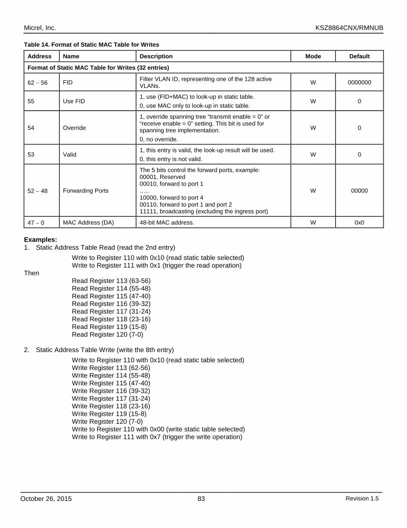
Micrel, Inc. KSZ8864CNX/RMNUB
October 26, 2015 83 Revision 1.5
Table 14. Format of Static MAC Table for Writes
Address Name Description Mode Default
Format of Static MAC Table for Writes (32 entries)
62 − 56 FID Filter VLAN ID, representing one of the 128 active VLANs. W 0000000
55 Use FID 1, use (FID+MAC) to look-up in static table. 0, use MAC only to look-up in static table.
W 0
54 Override
1, override spanning tree “transmit enable = 0” or “receive enable = 0” setting. This bit is used for spanning tree implementation. 0, no override.
W 0
53 Valid 1, this entry is valid, the look-up result will be used. 0, this entry is not valid.
W 0
52 − 48 Forwarding Ports
The 5 bits control the forward ports, example: 00001, Reserved 00010, forward to port 1 ….. 10000, forward to port 4 00110, forward to port 1 and port 2 11111, broadcasting (excluding the ingress port)
W 00000
47 − 0 MAC Address (DA) 48-bit MAC address. W 0x0 Examples: 1. Static Address Table Read (read the 2nd entry)
Write to Register 110 with 0x10 (read static table selected) Write to Register 111 with 0x1 (trigger the read operation)
Then Read Register 113 (63-56) Read Register 114 (55-48) Read Register 115 (47-40) Read Register 116 (39-32) Read Register 117 (31-24) Read Register 118 (23-16) Read Register 119 (15-8) Read Register 120 (7-0)
2. Static Address Table Write (write the 8th entry) Write to Register 110 with 0x10 (read static table selected) Write Register 113 (62-56) Write Register 114 (55-48) Write Register 115 (47-40) Write Register 116 (39-32) Write Register 117 (31-24) Write Register 118 (23-16) Write Register 119 (15-8) Write Register 120 (7-0) Write to Register 110 with 0x00 (write static table selected) Write to Register 111 with 0x7 (trigger the write operation)
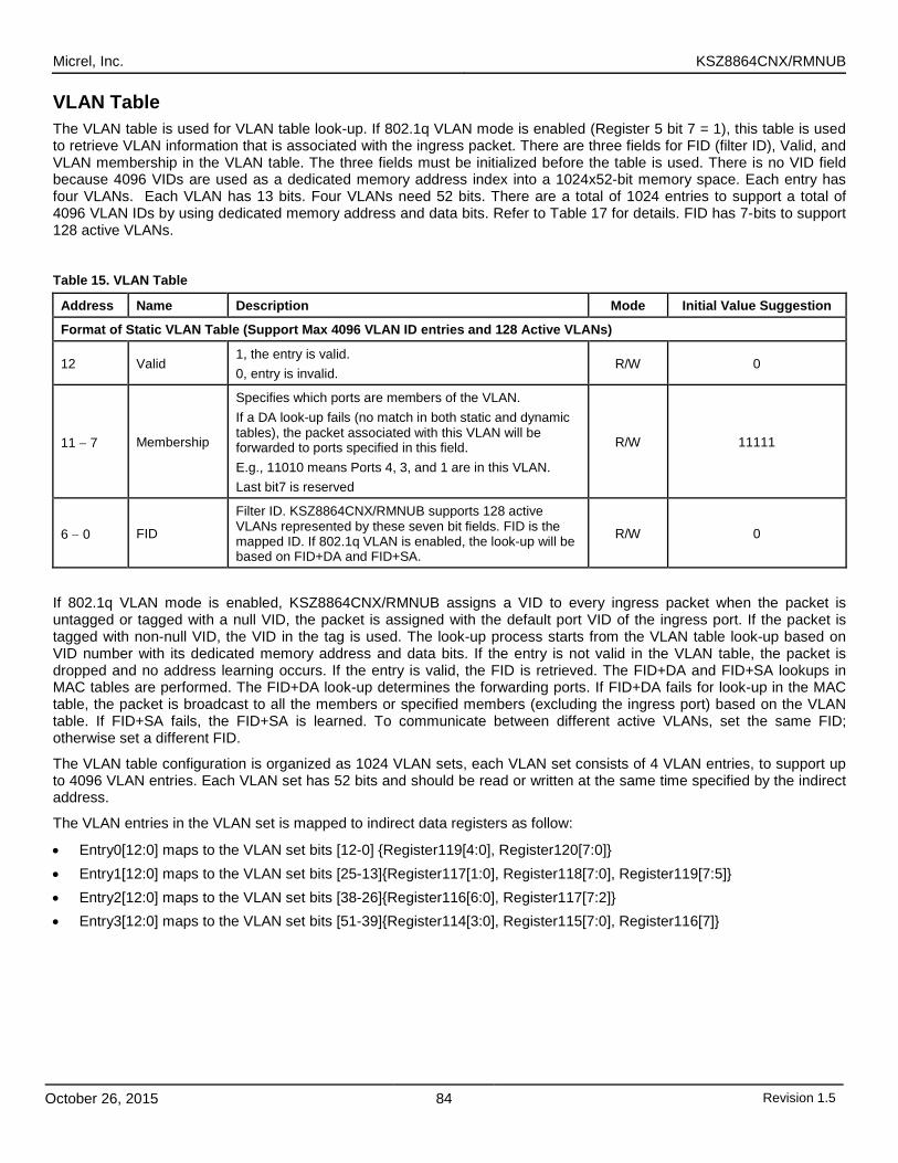
Micrel, Inc. KSZ8864CNX/RMNUB
October 26, 2015 84 Revision 1.5
VLAN Table The VLAN table is used for VLAN table look-up. If 802.1q VLAN mode is enabled (Register 5 bit 7 = 1), this table is used to retrieve VLAN information that is associated with the ingress packet. There are three fields for FID (filter ID), Valid, and VLAN membership in the VLAN table. The three fields must be initialized before the table is used. There is no VID field because 4096 VIDs are used as a dedicated memory address index into a 1024x52-bit memory space. Each entry has four VLANs. Each VLAN has 13 bits. Four VLANs need 52 bits. There are a total of 1024 entries to support a total of 4096 VLAN IDs by using dedicated memory address and data bits. Refer to Table 17 for details. FID has 7-bits to support 128 active VLANs.
Table 15. VLAN Table
Address Name Description Mode Initial Value Suggestion
Format of Static VLAN Table (Support Max 4096 VLAN ID entries and 128 Active VLANs)
12 Valid 1, the entry is valid. 0, entry is invalid.
R/W 0
11 − 7 Membership
Specifies which ports are members of the VLAN. If a DA look-up fails (no match in both static and dynamic tables), the packet associated with this VLAN will be forwarded to ports specified in this field. E.g., 11010 means Ports 4, 3, and 1 are in this VLAN. Last bit7 is reserved
R/W 11111
6 − 0 FID
Filter ID. KSZ8864CNX/RMNUB supports 128 active VLANs represented by these seven bit fields. FID is the mapped ID. If 802.1q VLAN is enabled, the look-up will be based on FID+DA and FID+SA.
R/W 0
If 802.1q VLAN mode is enabled, KSZ8864CNX/RMNUB assigns a VID to every ingress packet when the packet is untagged or tagged with a null VID, the packet is assigned with the default port VID of the ingress port. If the packet is tagged with non-null VID, the VID in the tag is used. The look-up process starts from the VLAN table look-up based on VID number with its dedicated memory address and data bits. If the entry is not valid in the VLAN table, the packet is dropped and no address learning occurs. If the entry is valid, the FID is retrieved. The FID+DA and FID+SA lookups in MAC tables are performed. The FID+DA look-up determines the forwarding ports. If FID+DA fails for look-up in the MAC table, the packet is broadcast to all the members or specified members (excluding the ingress port) based on the VLAN table. If FID+SA fails, the FID+SA is learned. To communicate between different active VLANs, set the same FID; otherwise set a different FID.
The VLAN table configuration is organized as 1024 VLAN sets, each VLAN set consists of 4 VLAN entries, to support up to 4096 VLAN entries. Each VLAN set has 52 bits and should be read or written at the same time specified by the indirect address.
The VLAN entries in the VLAN set is mapped to indirect data registers as follow:
• Entry0[12:0] maps to the VLAN set bits [12-0] Register119[4:0], Register120[7:0] • Entry1[12:0] maps to the VLAN set bits [25-13]Register117[1:0], Register118[7:0], Register119[7:5] • Entry2[12:0] maps to the VLAN set bits [38-26]Register116[6:0], Register117[7:2] • Entry3[12:0] maps to the VLAN set bits [51-39]Register114[3:0], Register115[7:0], Register116[7]
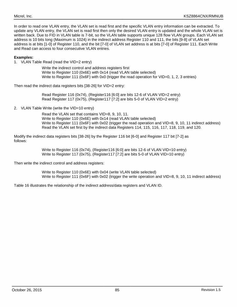
Micrel, Inc. KSZ8864CNX/RMNUB
October 26, 2015 85 Revision 1.5
In order to read one VLAN entry, the VLAN set is read first and the specific VLAN entry information can be extracted. To update any VLAN entry, the VLAN set is read first then only the desired VLAN entry is updated and the whole VLAN set is written back. Due to FID in VLAN table is 7-bit, so the VLAN table supports unique 128 flow VLAN groups. Each VLAN set address is 10 bits long (Maximum is 1024) in the indirect address Register 110 and 111, the bits [9-8] of VLAN set address is at bits [1-0] of Register 110, and the bit [7-0] of VLAN set address is at bits [7-0] of Register 111. Each Write and Read can access to four consecutive VLAN entries. Examples: 1. VLAN Table Read (read the VID=2 entry)
Write the indirect control and address registers first Write to Register 110 (0x6E) with 0x14 (read VLAN table selected) Write to Register 111 (0x6F) with 0x0 (trigger the read operation for VID=0, 1, 2, 3 entries)
Then read the indirect data registers bits [38-26] for VID=2 entry:
Read Register 116 (0x74), (Register116 [6:0] are bits 12-6 of VLAN VID=2 entry) Read Register 117 (0x75), (Register117 [7:2] are bits 5-0 of VLAN VID=2 entry)
2. VLAN Table Write (write the VID=10 entry) Read the VLAN set that contains VID=8, 9, 10, 11. Write to Register 110 (0x6E) with 0x14 (read VLAN table selected) Write to Register 111 (0x6F) with 0x02 (trigger the read operation and VID=8, 9, 10, 11 indirect address) Read the VLAN set first by the indirect data Registers 114, 115, 116, 117, 118, 119, and 120.
Modify the indirect data registers bits [38-26] by the Register 116 bit [6-0] and Register 117 bit [7-2] as follows:
Write to Register 116 (0x74), (Register116 [6:0] are bits 12-6 of VLAN VID=10 entry) Write to Register 117 (0x75), (Register117 [7:2] are bits 5-0 of VLAN VID=10 entry)
Then write the indirect control and address registers:
Write to Register 110 (0x6E) with 0x04 (write VLAN table selected) Write to Register 111 (0x6F) with 0x02 (trigger the write operation and VID=8, 9, 10, 11 indirect address)
Table 16 illustrates the relationship of the indirect address/data registers and VLAN ID.
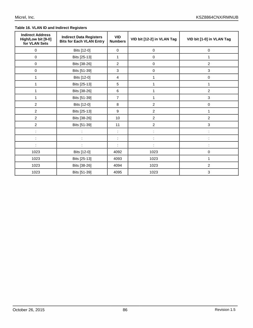
Micrel, Inc. KSZ8864CNX/RMNUB
October 26, 2015 86 Revision 1.5
Table 16. VLAN ID and Indirect Registers
Indirect Address High/Low bit [9-0]
for VLAN Sets Indirect Data Registers
Bits for Each VLAN Entry VID
Numbers VID bit [12-2] in VLAN Tag VID bit [1-0] in VLAN Tag
0 Bits [12-0] 0 0 0
0 Bits [25-13] 1 0 1
0 Bits [38-26] 2 0 2
0 Bits [51-39] 3 0 3
1 Bits [12-0] 4 1 0
1 Bits [25-13] 5 1 1
1 Bits [38-26] 6 1 2
1 Bits [51-39] 7 1 3
2 Bits [12-0] 8 2 0
2 Bits [25-13] 9 2 1
2 Bits [38-26] 10 2 2
2 Bits [51-39] 11 2 3
: : : : :
: : : : :
: : : : :
1023 Bits [12-0] 4092 1023 0
1023 Bits [25-13] 4093 1023 1
1023 Bits [38-26] 4094 1023 2
1023 Bits [51-39] 4095 1023 3
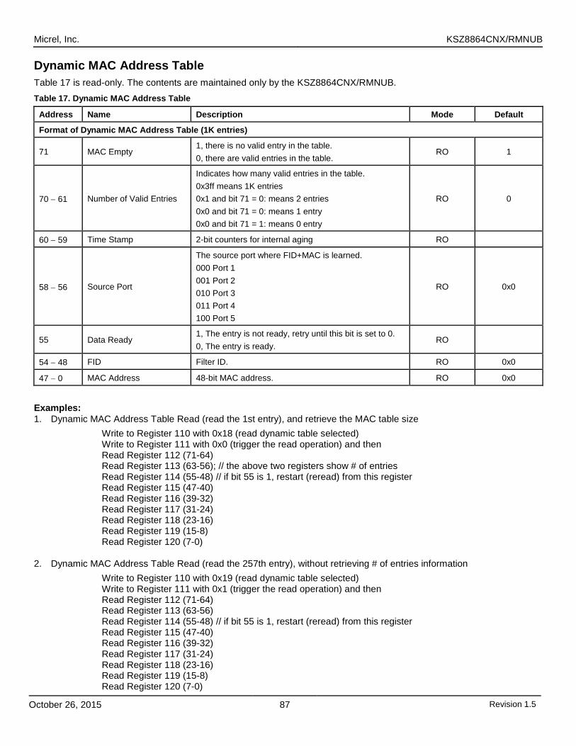
Micrel, Inc. KSZ8864CNX/RMNUB
October 26, 2015 87 Revision 1.5
Dynamic MAC Address Table Table 17 is read-only. The contents are maintained only by the KSZ8864CNX/RMNUB. Table 17. Dynamic MAC Address Table
Address Name Description Mode Default
Format of Dynamic MAC Address Table (1K entries)
71 MAC Empty 1, there is no valid entry in the table. 0, there are valid entries in the table.
RO 1
70 − 61 Number of Valid Entries
Indicates how many valid entries in the table. 0x3ff means 1K entries 0x1 and bit 71 = 0: means 2 entries 0x0 and bit 71 = 0: means 1 entry 0x0 and bit 71 = 1: means 0 entry
RO 0
60 − 59 Time Stamp 2-bit counters for internal aging RO
58 − 56 Source Port
The source port where FID+MAC is learned. 000 Port 1 001 Port 2 010 Port 3 011 Port 4 100 Port 5
RO 0x0
55 Data Ready 1, The entry is not ready, retry until this bit is set to 0. 0, The entry is ready.
RO
54 − 48 FID Filter ID. RO 0x0
47 − 0 MAC Address 48-bit MAC address. RO 0x0
Examples: 1. Dynamic MAC Address Table Read (read the 1st entry), and retrieve the MAC table size
Write to Register 110 with 0x18 (read dynamic table selected) Write to Register 111 with 0x0 (trigger the read operation) and then Read Register 112 (71-64) Read Register 113 (63-56); // the above two registers show # of entries Read Register 114 (55-48) // if bit 55 is 1, restart (reread) from this register Read Register 115 (47-40) Read Register 116 (39-32) Read Register 117 (31-24) Read Register 118 (23-16) Read Register 119 (15-8) Read Register 120 (7-0)
2. Dynamic MAC Address Table Read (read the 257th entry), without retrieving # of entries information
Write to Register 110 with 0x19 (read dynamic table selected) Write to Register 111 with 0x1 (trigger the read operation) and then Read Register 112 (71-64) Read Register 113 (63-56) Read Register 114 (55-48) // if bit 55 is 1, restart (reread) from this register Read Register 115 (47-40) Read Register 116 (39-32) Read Register 117 (31-24) Read Register 118 (23-16) Read Register 119 (15-8) Read Register 120 (7-0)
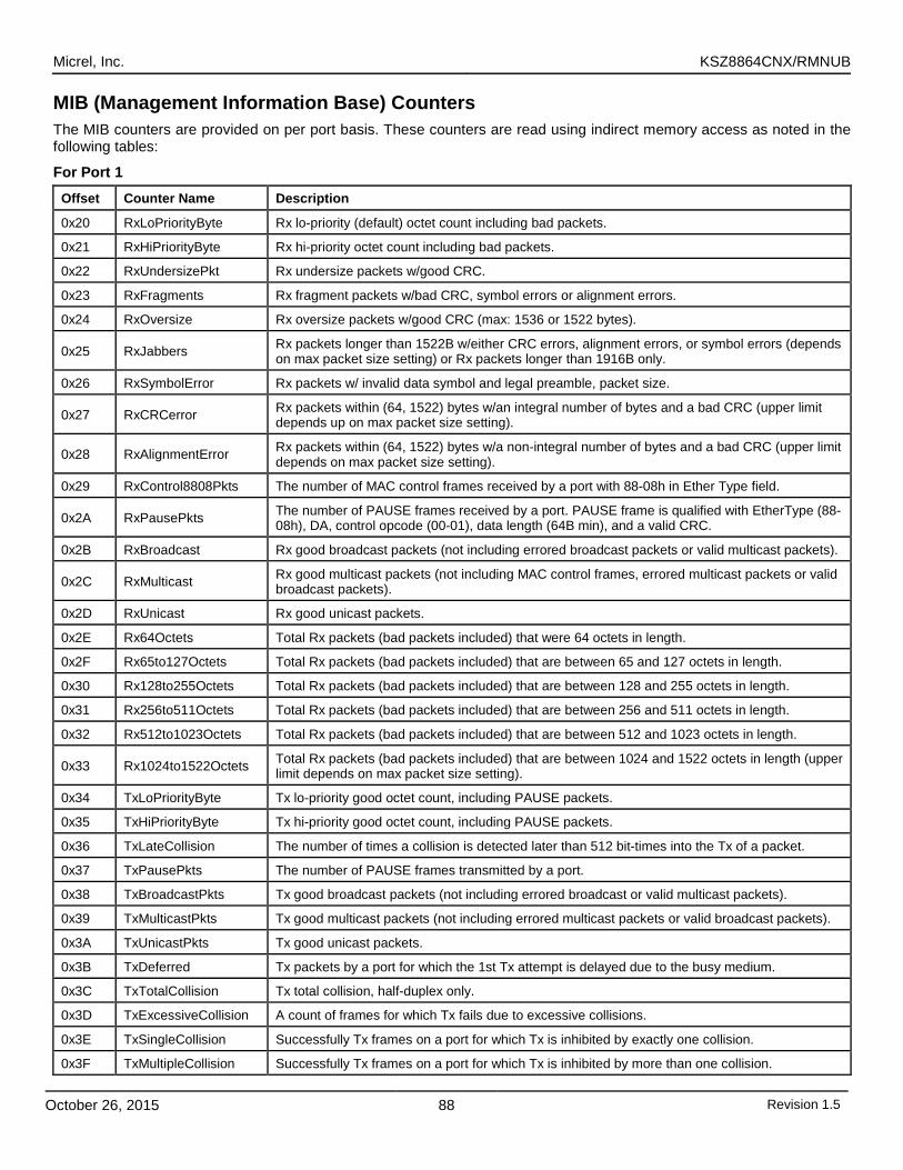
Micrel, Inc. KSZ8864CNX/RMNUB
October 26, 2015 88 Revision 1.5
MIB (Management Information Base) Counters The MIB counters are provided on per port basis. These counters are read using indirect memory access as noted in the following tables:
For Port 1
Offset Counter Name Description
0x20 RxLoPriorityByte Rx lo-priority (default) octet count including bad packets.
0x21 RxHiPriorityByte Rx hi-priority octet count including bad packets.
0x22 RxUndersizePkt Rx undersize packets w/good CRC.
0x23 RxFragments Rx fragment packets w/bad CRC, symbol errors or alignment errors.
0x24 RxOversize Rx oversize packets w/good CRC (max: 1536 or 1522 bytes).
0x25 RxJabbers Rx packets longer than 1522B w/either CRC errors, alignment errors, or symbol errors (depends on max packet size setting) or Rx packets longer than 1916B only.
0x26 RxSymbolError Rx packets w/ invalid data symbol and legal preamble, packet size.
0x27 RxCRCerror Rx packets within (64, 1522) bytes w/an integral number of bytes and a bad CRC (upper limit depends up on max packet size setting).
0x28 RxAlignmentError Rx packets within (64, 1522) bytes w/a non-integral number of bytes and a bad CRC (upper limit depends on max packet size setting).
0x29 RxControl8808Pkts The number of MAC control frames received by a port with 88-08h in Ether Type field.
0x2A RxPausePkts The number of PAUSE frames received by a port. PAUSE frame is qualified with EtherType (88-08h), DA, control opcode (00-01), data length (64B min), and a valid CRC.
0x2B RxBroadcast Rx good broadcast packets (not including errored broadcast packets or valid multicast packets).
0x2C RxMulticast Rx good multicast packets (not including MAC control frames, errored multicast packets or valid broadcast packets).
0x2D RxUnicast Rx good unicast packets.
0x2E Rx64Octets Total Rx packets (bad packets included) that were 64 octets in length.
0x2F Rx65to127Octets Total Rx packets (bad packets included) that are between 65 and 127 octets in length.
0x30 Rx128to255Octets Total Rx packets (bad packets included) that are between 128 and 255 octets in length.
0x31 Rx256to511Octets Total Rx packets (bad packets included) that are between 256 and 511 octets in length.
0x32 Rx512to1023Octets Total Rx packets (bad packets included) that are between 512 and 1023 octets in length.
0x33 Rx1024to1522Octets Total Rx packets (bad packets included) that are between 1024 and 1522 octets in length (upper limit depends on max packet size setting).
0x34 TxLoPriorityByte Tx lo-priority good octet count, including PAUSE packets.
0x35 TxHiPriorityByte Tx hi-priority good octet count, including PAUSE packets.
0x36 TxLateCollision The number of times a collision is detected later than 512 bit-times into the Tx of a packet.
0x37 TxPausePkts The number of PAUSE frames transmitted by a port.
0x38 TxBroadcastPkts Tx good broadcast packets (not including errored broadcast or valid multicast packets).
0x39 TxMulticastPkts Tx good multicast packets (not including errored multicast packets or valid broadcast packets).
0x3A TxUnicastPkts Tx good unicast packets.
0x3B TxDeferred Tx packets by a port for which the 1st Tx attempt is delayed due to the busy medium.
0x3C TxTotalCollision Tx total collision, half-duplex only.
0x3D TxExcessiveCollision A count of frames for which Tx fails due to excessive collisions.
0x3E TxSingleCollision Successfully Tx frames on a port for which Tx is inhibited by exactly one collision.
0x3F TxMultipleCollision Successfully Tx frames on a port for which Tx is inhibited by more than one collision.
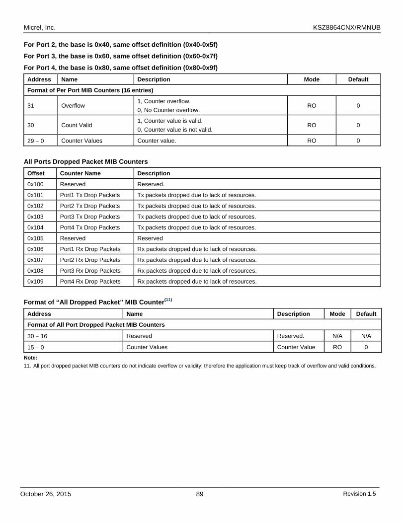
Micrel, Inc. KSZ8864CNX/RMNUB
October 26, 2015 89 Revision 1.5
For Port 2, the base is 0x40, same offset definition (0x40-0x5f)
For Port 3, the base is 0x60, same offset definition (0x60-0x7f)
For Port 4, the base is 0x80, same offset definition (0x80-0x9f)
Address Name Description Mode Default
Format of Per Port MIB Counters (16 entries)
31 Overflow 1, Counter overflow. 0, No Counter overflow.
RO 0
30 Count Valid 1, Counter value is valid. 0, Counter value is not valid.
RO 0
29 − 0 Counter Values Counter value. RO 0
All Ports Dropped Packet MIB Counters
Offset Counter Name Description
0x100 Reserved Reserved.
0x101 Port1 Tx Drop Packets Tx packets dropped due to lack of resources.
0x102 Port2 Tx Drop Packets Tx packets dropped due to lack of resources.
0x103 Port3 Tx Drop Packets Tx packets dropped due to lack of resources.
0x104 Port4 Tx Drop Packets Tx packets dropped due to lack of resources.
0x105 Reserved Reserved
0x106 Port1 Rx Drop Packets Rx packets dropped due to lack of resources.
0x107 Port2 Rx Drop Packets Rx packets dropped due to lack of resources.
0x108 Port3 Rx Drop Packets Rx packets dropped due to lack of resources.
0x109 Port4 Rx Drop Packets Rx packets dropped due to lack of resources.
Format of “All Dropped Packet” MIB Counter(11)
Address Name Description Mode Default
Format of All Port Dropped Packet MIB Counters
30 − 16 Reserved Reserved. N/A N/A
15 − 0 Counter Values Counter Value RO 0
Note: 11. All port dropped packet MIB counters do not indicate overflow or validity; therefore the application must keep track of overflow and valid conditions.
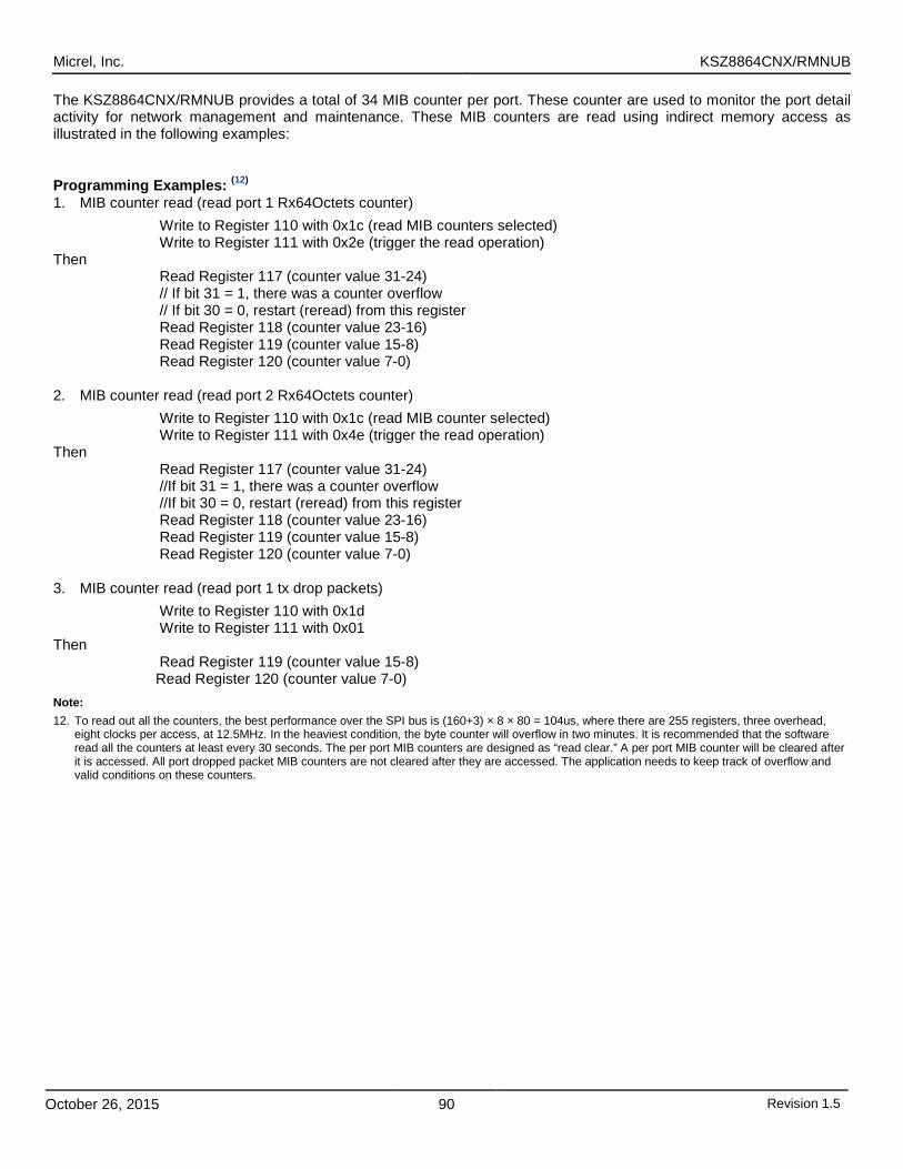
Micrel, Inc. KSZ8864CNX/RMNUB
October 26, 2015 90 Revision 1.5
The KSZ8864CNX/RMNUB provides a total of 34 MIB counter per port. These counter are used to monitor the port detail activity for network management and maintenance. These MIB counters are read using indirect memory access as illustrated in the following examples:
Programming Examples: (12) 1. MIB counter read (read port 1 Rx64Octets counter)
Write to Register 110 with 0x1c (read MIB counters selected) Write to Register 111 with 0x2e (trigger the read operation)
Then Read Register 117 (counter value 31-24) // If bit 31 = 1, there was a counter overflow // If bit 30 = 0, restart (reread) from this register Read Register 118 (counter value 23-16) Read Register 119 (counter value 15-8) Read Register 120 (counter value 7-0)
2. MIB counter read (read port 2 Rx64Octets counter)
Write to Register 110 with 0x1c (read MIB counter selected) Write to Register 111 with 0x4e (trigger the read operation)
Then Read Register 117 (counter value 31-24) //If bit 31 = 1, there was a counter overflow //If bit 30 = 0, restart (reread) from this register Read Register 118 (counter value 23-16) Read Register 119 (counter value 15-8) Read Register 120 (counter value 7-0)
3. MIB counter read (read port 1 tx drop packets)
Write to Register 110 with 0x1d Write to Register 111 with 0x01
Then Read Register 119 (counter value 15-8)
Read Register 120 (counter value 7-0) Note: 12. To read out all the counters, the best performance over the SPI bus is (160+3) × 8 × 80 = 104us, where there are 255 registers, three overhead,
eight clocks per access, at 12.5MHz. In the heaviest condition, the byte counter will overflow in two minutes. It is recommended that the software read all the counters at least every 30 seconds. The per port MIB counters are designed as “read clear.” A per port MIB counter will be cleared after it is accessed. All port dropped packet MIB counters are not cleared after they are accessed. The application needs to keep track of overflow and valid conditions on these counters.
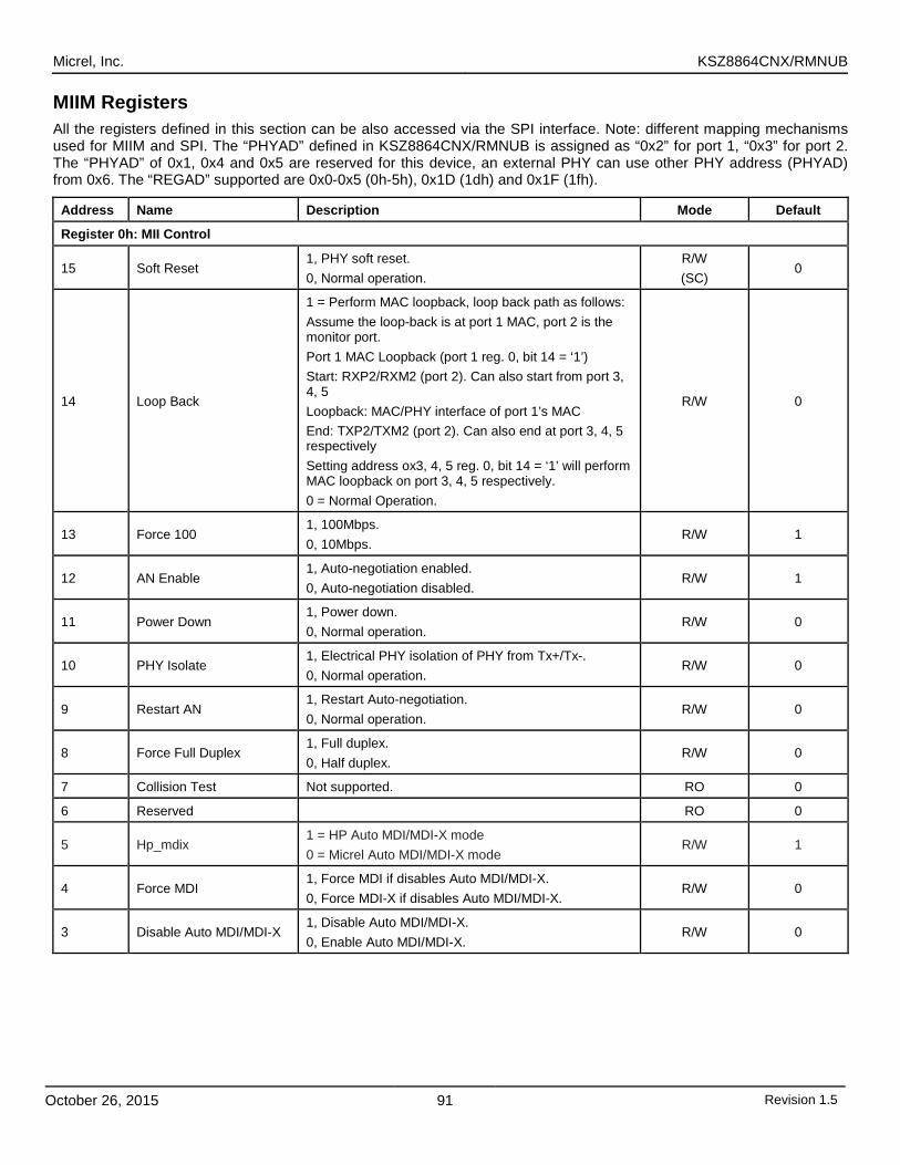
Micrel, Inc. KSZ8864CNX/RMNUB
October 26, 2015 91 Revision 1.5
MIIM Registers All the registers defined in this section can be also accessed via the SPI interface. Note: different mapping mechanisms used for MIIM and SPI. The “PHYAD” defined in KSZ8864CNX/RMNUB is assigned as “0x2” for port 1, “0x3” for port 2. The “PHYAD” of 0x1, 0x4 and 0x5 are reserved for this device, an external PHY can use other PHY address (PHYAD) from 0x6. The “REGAD” supported are 0x0-0x5 (0h-5h), 0x1D (1dh) and 0x1F (1fh).
Address Name Description Mode Default
Register 0h: MII Control
15 Soft Reset 1, PHY soft reset. 0, Normal operation.
R/W (SC)
0
14 Loop Back
1 = Perform MAC loopback, loop back path as follows: Assume the loop-back is at port 1 MAC, port 2 is the monitor port. Port 1 MAC Loopback (port 1 reg. 0, bit 14 = ‘1’) Start: RXP2/RXM2 (port 2). Can also start from port 3, 4, 5 Loopback: MAC/PHY interface of port 1’s MAC End: TXP2/TXM2 (port 2). Can also end at port 3, 4, 5 respectively Setting address ox3, 4, 5 reg. 0, bit 14 = ‘1’ will perform MAC loopback on port 3, 4, 5 respectively. 0 = Normal Operation.
R/W 0
13 Force 100 1, 100Mbps. 0, 10Mbps.
R/W 1
12 AN Enable 1, Auto-negotiation enabled. 0, Auto-negotiation disabled.
R/W 1
11 Power Down 1, Power down. 0, Normal operation.
R/W 0
10 PHY Isolate 1, Electrical PHY isolation of PHY from Tx+/Tx-. 0, Normal operation.
R/W 0
9 Restart AN 1, Restart Auto-negotiation. 0, Normal operation.
R/W 0
8 Force Full Duplex 1, Full duplex. 0, Half duplex.
R/W 0
7 Collision Test Not supported. RO 0
6 Reserved RO 0
5 Hp_mdix 1 = HP Auto MDI/MDI-X mode 0 = Micrel Auto MDI/MDI-X mode
R/W 1
4 Force MDI 1, Force MDI if disables Auto MDI/MDI-X. 0, Force MDI-X if disables Auto MDI/MDI-X.
R/W 0
3 Disable Auto MDI/MDI-X 1, Disable Auto MDI/MDI-X. 0, Enable Auto MDI/MDI-X.
R/W 0
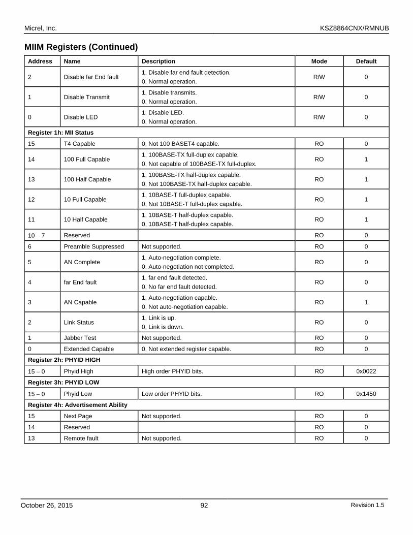
Micrel, Inc. KSZ8864CNX/RMNUB
October 26, 2015 92 Revision 1.5
MIIM Registers (Continued)
Address Name Description Mode Default
2 Disable far End fault 1, Disable far end fault detection. 0, Normal operation.
R/W 0
1 Disable Transmit 1, Disable transmits. 0, Normal operation.
R/W 0
0 Disable LED 1, Disable LED. 0, Normal operation.
R/W 0
Register 1h: MII Status
15 T4 Capable 0, Not 100 BASET4 capable. RO 0
14 100 Full Capable 1, 100BASE-TX full-duplex capable. 0, Not capable of 100BASE-TX full-duplex.
RO 1
13 100 Half Capable 1, 100BASE-TX half-duplex capable. 0, Not 100BASE-TX half-duplex capable.
RO 1
12 10 Full Capable 1, 10BASE-T full-duplex capable. 0, Not 10BASE-T full-duplex capable.
RO 1
11 10 Half Capable 1, 10BASE-T half-duplex capable. 0, 10BASE-T half-duplex capable.
RO 1
10 − 7 Reserved RO 0
6 Preamble Suppressed Not supported. RO 0
5 AN Complete 1, Auto-negotiation complete. 0, Auto-negotiation not completed.
RO 0
4 far End fault 1, far end fault detected. 0, No far end fault detected.
RO 0
3 AN Capable 1, Auto-negotiation capable. 0, Not auto-negotiation capable.
RO 1
2 Link Status 1, Link is up. 0, Link is down.
RO 0
1 Jabber Test Not supported. RO 0
0 Extended Capable 0, Not extended register capable. RO 0
Register 2h: PHYID HIGH
15 − 0 Phyid High High order PHYID bits. RO 0x0022
Register 3h: PHYID LOW
15 − 0 Phyid Low Low order PHYID bits. RO 0x1450
Register 4h: Advertisement Ability
15 Next Page Not supported. RO 0
14 Reserved RO 0
13 Remote fault Not supported. RO 0
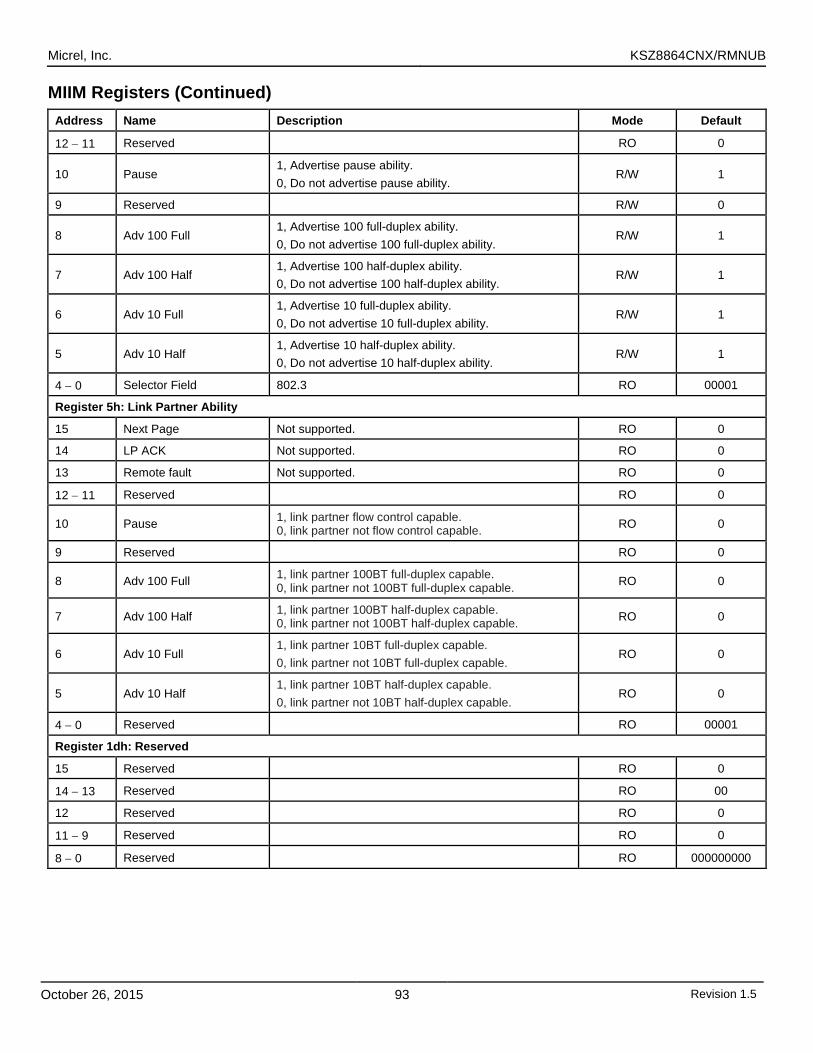
Micrel, Inc. KSZ8864CNX/RMNUB
October 26, 2015 93 Revision 1.5
MIIM Registers (Continued)
Address Name Description Mode Default
12 − 11 Reserved RO 0
10 Pause 1, Advertise pause ability. 0, Do not advertise pause ability.
R/W 1
9 Reserved R/W 0
8 Adv 100 Full 1, Advertise 100 full-duplex ability. 0, Do not advertise 100 full-duplex ability.
R/W 1
7 Adv 100 Half 1, Advertise 100 half-duplex ability. 0, Do not advertise 100 half-duplex ability.
R/W 1
6 Adv 10 Full 1, Advertise 10 full-duplex ability. 0, Do not advertise 10 full-duplex ability.
R/W 1
5 Adv 10 Half 1, Advertise 10 half-duplex ability. 0, Do not advertise 10 half-duplex ability.
R/W 1
4 − 0 Selector Field 802.3 RO 00001
Register 5h: Link Partner Ability
15 Next Page Not supported. RO 0
14 LP ACK Not supported. RO 0
13 Remote fault Not supported. RO 0
12 − 11 Reserved RO 0
10 Pause 1, link partner flow control capable. 0, link partner not flow control capable. RO 0
9 Reserved RO 0
8 Adv 100 Full 1, link partner 100BT full-duplex capable. 0, link partner not 100BT full-duplex capable. RO 0
7 Adv 100 Half 1, link partner 100BT half-duplex capable. 0, link partner not 100BT half-duplex capable. RO 0
6 Adv 10 Full 1, link partner 10BT full-duplex capable. 0, link partner not 10BT full-duplex capable.
RO 0
5 Adv 10 Half 1, link partner 10BT half-duplex capable. 0, link partner not 10BT half-duplex capable.
RO 0
4 − 0 Reserved RO 00001
Register 1dh: Reserved
15 Reserved RO 0
14 − 13 Reserved RO 00
12 Reserved RO 0
11 − 9 Reserved RO 0
8 − 0 Reserved RO 000000000
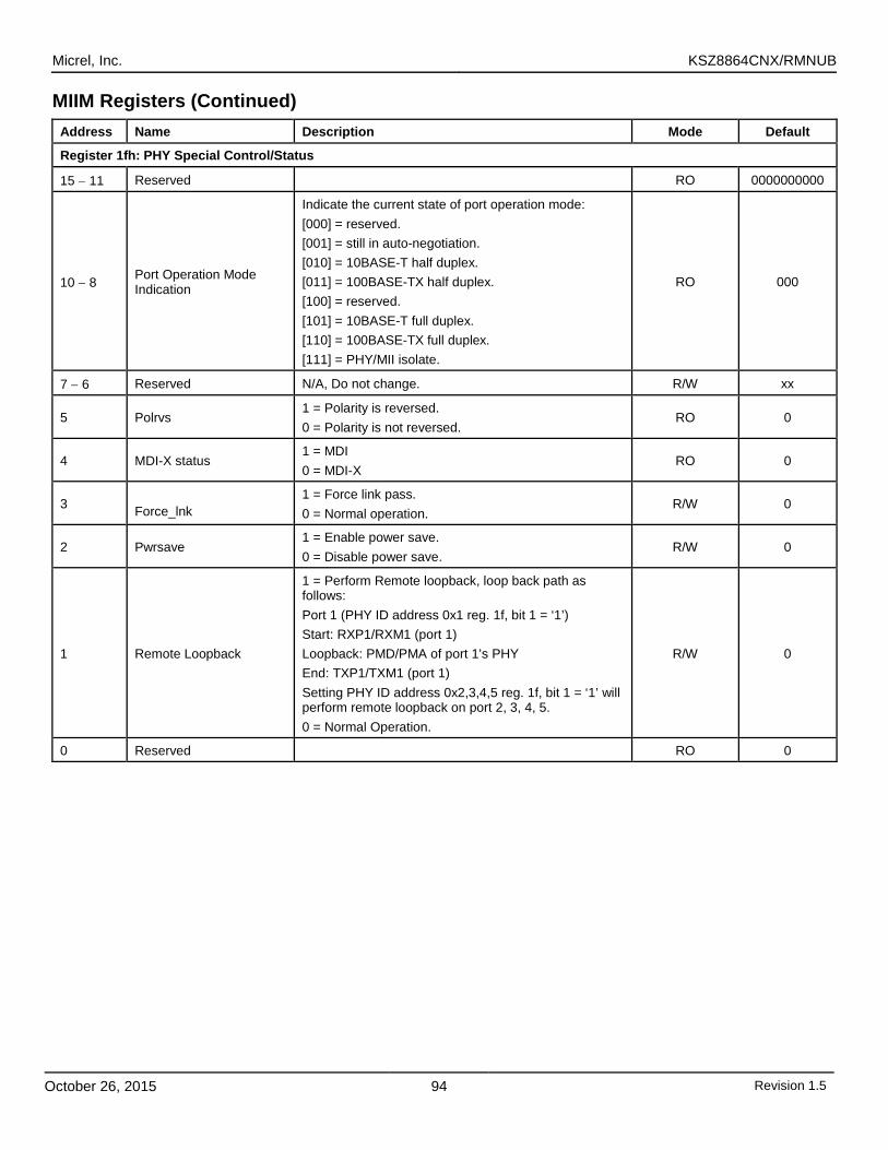
Micrel, Inc. KSZ8864CNX/RMNUB
October 26, 2015 94 Revision 1.5
MIIM Registers (Continued)
Address Name Description Mode Default
Register 1fh: PHY Special Control/Status
15 − 11 Reserved RO 0000000000
10 − 8 Port Operation Mode Indication
Indicate the current state of port operation mode: [000] = reserved. [001] = still in auto-negotiation. [010] = 10BASE-T half duplex. [011] = 100BASE-TX half duplex. [100] = reserved. [101] = 10BASE-T full duplex. [110] = 100BASE-TX full duplex. [111] = PHY/MII isolate.
RO 000
7 − 6 Reserved N/A, Do not change. R/W xx
5 Polrvs 1 = Polarity is reversed. 0 = Polarity is not reversed.
RO 0
4 MDI-X status 1 = MDI 0 = MDI-X
RO 0
3 Force_lnk
1 = Force link pass. 0 = Normal operation.
R/W 0
2 Pwrsave 1 = Enable power save. 0 = Disable power save.
R/W 0
1 Remote Loopback
1 = Perform Remote loopback, loop back path as follows: Port 1 (PHY ID address 0x1 reg. 1f, bit 1 = ‘1’) Start: RXP1/RXM1 (port 1) Loopback: PMD/PMA of port 1’s PHY End: TXP1/TXM1 (port 1) Setting PHY ID address 0x2,3,4,5 reg. 1f, bit 1 = ‘1’ will perform remote loopback on port 2, 3, 4, 5. 0 = Normal Operation.
R/W 0
0 Reserved RO 0
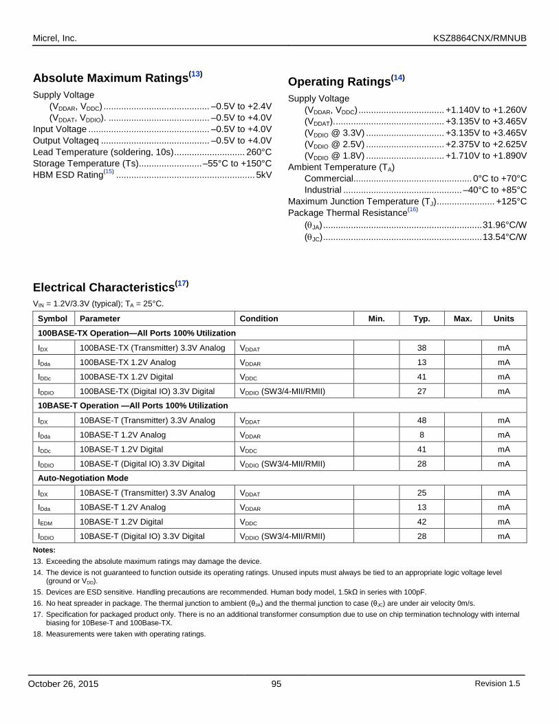
Micrel, Inc. KSZ8864CNX/RMNUB
October 26, 2015 95 Revision 1.5
Absolute Maximum Ratings(13) Supply Voltage (VDDAR, VDDC) .......................................... –0.5V to +2.4V (VDDAT, VDDIO). ........................................ –0.5V to +4.0V Input Voltage ................................................ –0.5V to +4.0V Output Voltageq ........................................... –0.5V to +4.0V Lead Temperature (soldering, 10s) ............................ 260°C Storage Temperature (Ts) ......................... –55°C to +150°C HBM ESD Rating(15) ....................................................... 5kV
Operating Ratings(14) Supply Voltage (VDDAR, VDDC) .................................. +1.140V to +1.260V (VDDAT). ........................................... +3.135V to +3.465V (VDDIO @ 3.3V) ............................... +3.135V to +3.465V (VDDIO @ 2.5V) ............................... +2.375V to +2.625V (VDDIO @ 1.8V) ............................... +1.710V to +1.890V Ambient Temperature (TA) Commercial............................................... 0°C to +70°C Industrial ............................................... –40°C to +85°C Maximum Junction Temperature (TJ) ....................... +125°C Package Thermal Resistance(16) (θJA) ............................................................... 31.96°C/W (θJC) ............................................................... 13.54°C/W
Electrical Characteristics(17) VIN = 1.2V/3.3V (typical); TA = 25°C.
Symbol Parameter Condition Min. Typ. Max. Units
100BASE-TX Operation—All Ports 100% Utilization
IDX 100BASE-TX (Transmitter) 3.3V Analog VDDAT 38 mA
IDda 100BASE-TX 1.2V Analog VDDAR 13 mA
IDDc 100BASE-TX 1.2V Digital VDDC 41 mA
IDDIO 100BASE-TX (Digital IO) 3.3V Digital VDDIO (SW3/4-MII/RMII) 27 mA
10BASE-T Operation —All Ports 100% Utilization
IDX 10BASE-T (Transmitter) 3.3V Analog VDDAT 48 mA
IDda 10BASE-T 1.2V Analog VDDAR 8 mA
IDDc 10BASE-T 1.2V Digital VDDC 41 mA
IDDIO 10BASE-T (Digital IO) 3.3V Digital VDDIO (SW3/4-MII/RMII) 28 mA
Auto-Negotiation Mode
IDX 10BASE-T (Transmitter) 3.3V Analog VDDAT 25 mA
IDda 10BASE-T 1.2V Analog VDDAR 13 mA
IEDM 10BASE-T 1.2V Digital VDDC 42 mA
IDDIO 10BASE-T (Digital IO) 3.3V Digital VDDIO (SW3/4-MII/RMII) 28 mA Notes: 13. Exceeding the absolute maximum ratings may damage the device. 14. The device is not guaranteed to function outside its operating ratings. Unused inputs must always be tied to an appropriate logic voltage level
(ground or VDD). 15. Devices are ESD sensitive. Handling precautions are recommended. Human body model, 1.5kΩ in series with 100pF. 16. No heat spreader in package. The thermal junction to ambient (θJA) and the thermal junction to case (θJC) are under air velocity 0m/s. 17. Specification for packaged product only. There is no an additional transformer consumption due to use on chip termination technology with internal
biasing for 10Bese-T and 100Base-TX. 18. Measurements were taken with operating ratings.
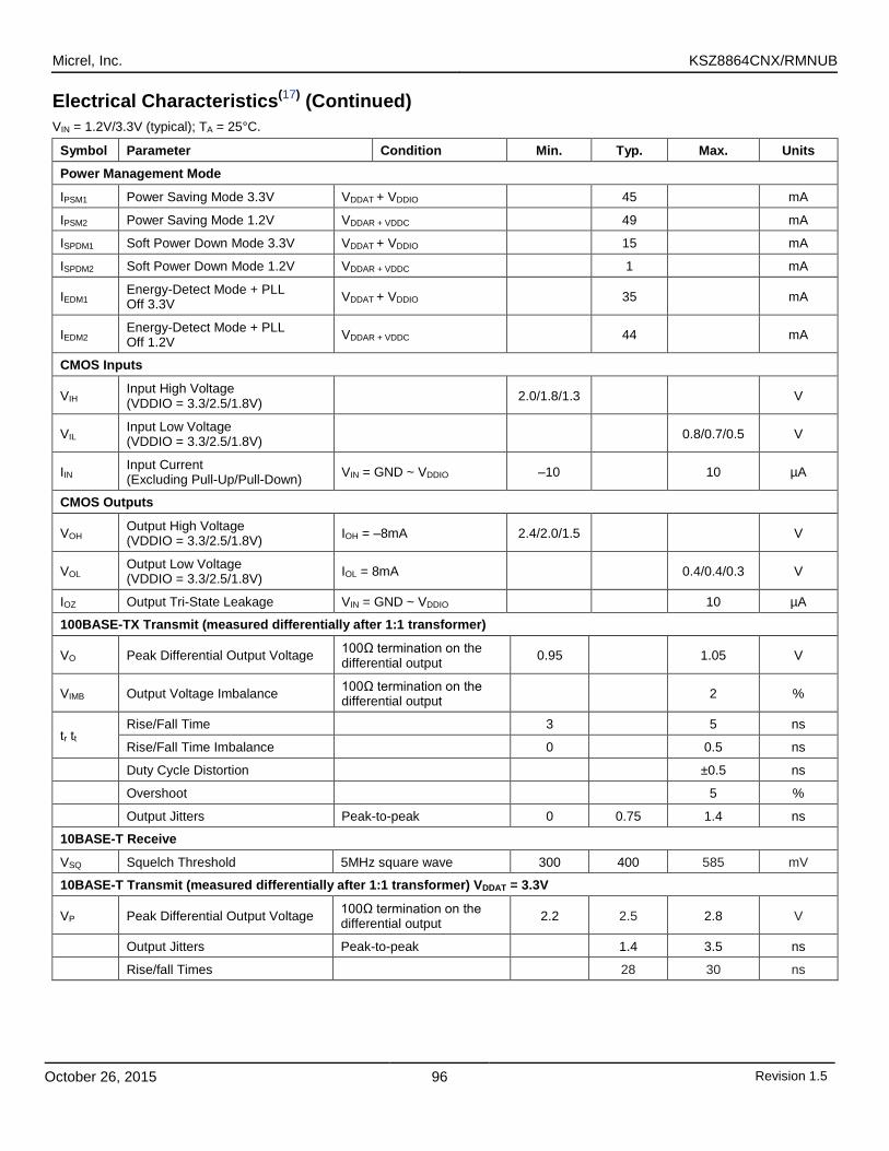
Micrel, Inc. KSZ8864CNX/RMNUB
October 26, 2015 96 Revision 1.5
Electrical Characteristics(17) (Continued) VIN = 1.2V/3.3V (typical); TA = 25°C.
Symbol Parameter Condition Min. Typ. Max. Units
Power Management Mode
IPSM1 Power Saving Mode 3.3V VDDAT + VDDIO 45 mA
IPSM2 Power Saving Mode 1.2V VDDAR + VDDC 49 mA
ISPDM1 Soft Power Down Mode 3.3V VDDAT + VDDIO 15 mA
ISPDM2 Soft Power Down Mode 1.2V VDDAR + VDDC 1 mA
IEDM1 Energy-Detect Mode + PLL Off 3.3V VDDAT + VDDIO 35 mA
IEDM2 Energy-Detect Mode + PLL Off 1.2V VDDAR + VDDC 44 mA
CMOS Inputs
VIH Input High Voltage (VDDIO = 3.3/2.5/1.8V) 2.0/1.8/1.3 V
VIL Input Low Voltage (VDDIO = 3.3/2.5/1.8V) 0.8/0.7/0.5 V
IIN Input Current (Excluding Pull-Up/Pull-Down) VIN = GND ~ VDDIO –10 10 µA
CMOS Outputs
VOH Output High Voltage (VDDIO = 3.3/2.5/1.8V) IOH = –8mA 2.4/2.0/1.5 V
VOL Output Low Voltage (VDDIO = 3.3/2.5/1.8V) IOL = 8mA 0.4/0.4/0.3 V
IOZ Output Tri-State Leakage VIN = GND ~ VDDIO 10 µA
100BASE-TX Transmit (measured differentially after 1:1 transformer)
VO Peak Differential Output Voltage 100Ω termination on the differential output 0.95 1.05 V
VIMB Output Voltage Imbalance 100Ω termination on the differential output 2 %
tr tt Rise/Fall Time 3 5 ns
Rise/Fall Time Imbalance 0 0.5 ns
Duty Cycle Distortion ±0.5 ns
Overshoot 5 %
Output Jitters Peak-to-peak 0 0.75 1.4 ns
10BASE-T Receive
VSQ Squelch Threshold 5MHz square wave 300 400 585 mV
10BASE-T Transmit (measured differentially after 1:1 transformer) VDDAT = 3.3V
VP Peak Differential Output Voltage 100Ω termination on the differential output 2.2 2.5 2.8 V
Output Jitters Peak-to-peak 1.4 3.5 ns
Rise/fall Times 28 30 ns
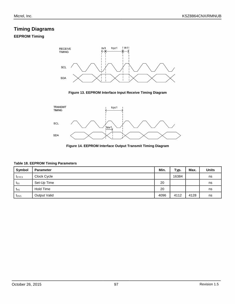
Micrel, Inc. KSZ8864CNX/RMNUB
October 26, 2015 97 Revision 1.5
Timing Diagrams EEPROM Timing
Figure 13. EEPROM Interface Input Receive Timing Diagram
Figure 14. EEPROM Interface Output Transmit Timing Diagram
Table 18. EEPROM Timing Parameters
Symbol Parameter Min. Typ. Max. Units
tCYC1 Clock Cycle 16384 ns
tS1 Set-Up Time 20 ns
tH1 Hold Time 20 ns
tOV1 Output Valid 4096 4112 4128 ns
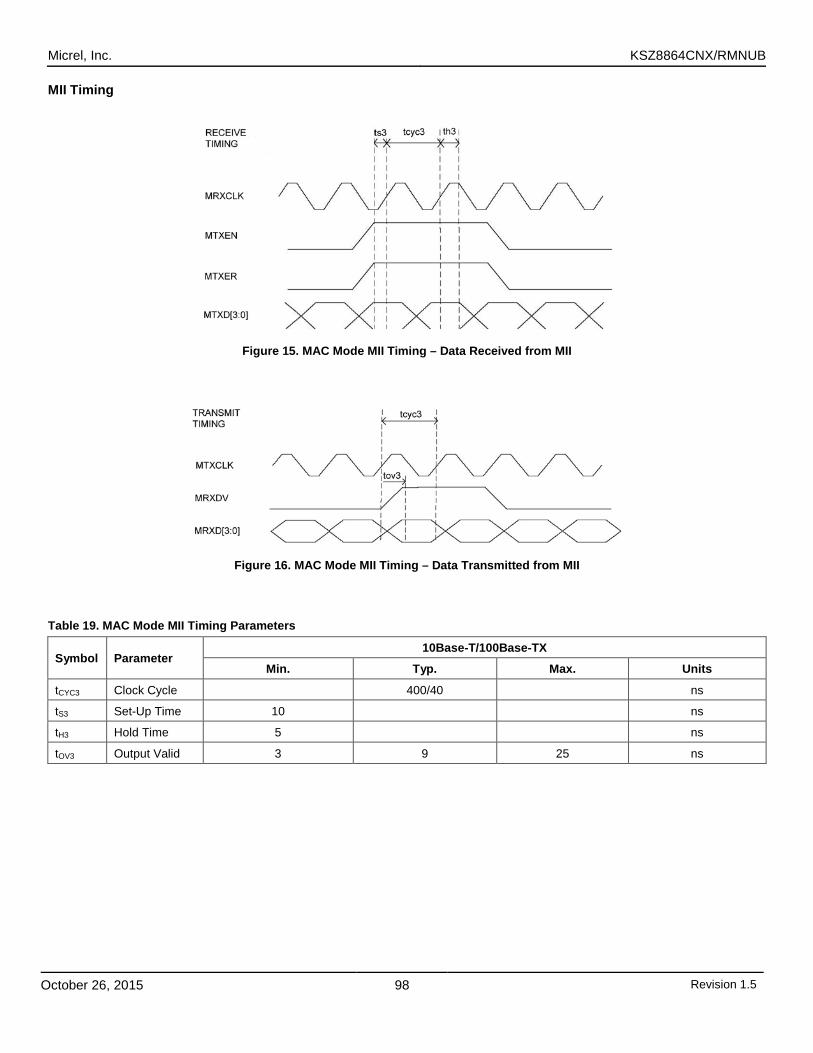
Micrel, Inc. KSZ8864CNX/RMNUB
October 26, 2015 98 Revision 1.5
MII Timing
Figure 15. MAC Mode MII Timing – Data Received from MII
Figure 16. MAC Mode MII Timing – Data Transmitted from MII
Table 19. MAC Mode MII Timing Parameters
Symbol Parameter 10Base-T/100Base-TX
Min. Typ. Max. Units
tCYC3 Clock Cycle 400/40 ns
tS3 Set-Up Time 10 ns
tH3 Hold Time 5 ns
tOV3 Output Valid 3 9 25 ns
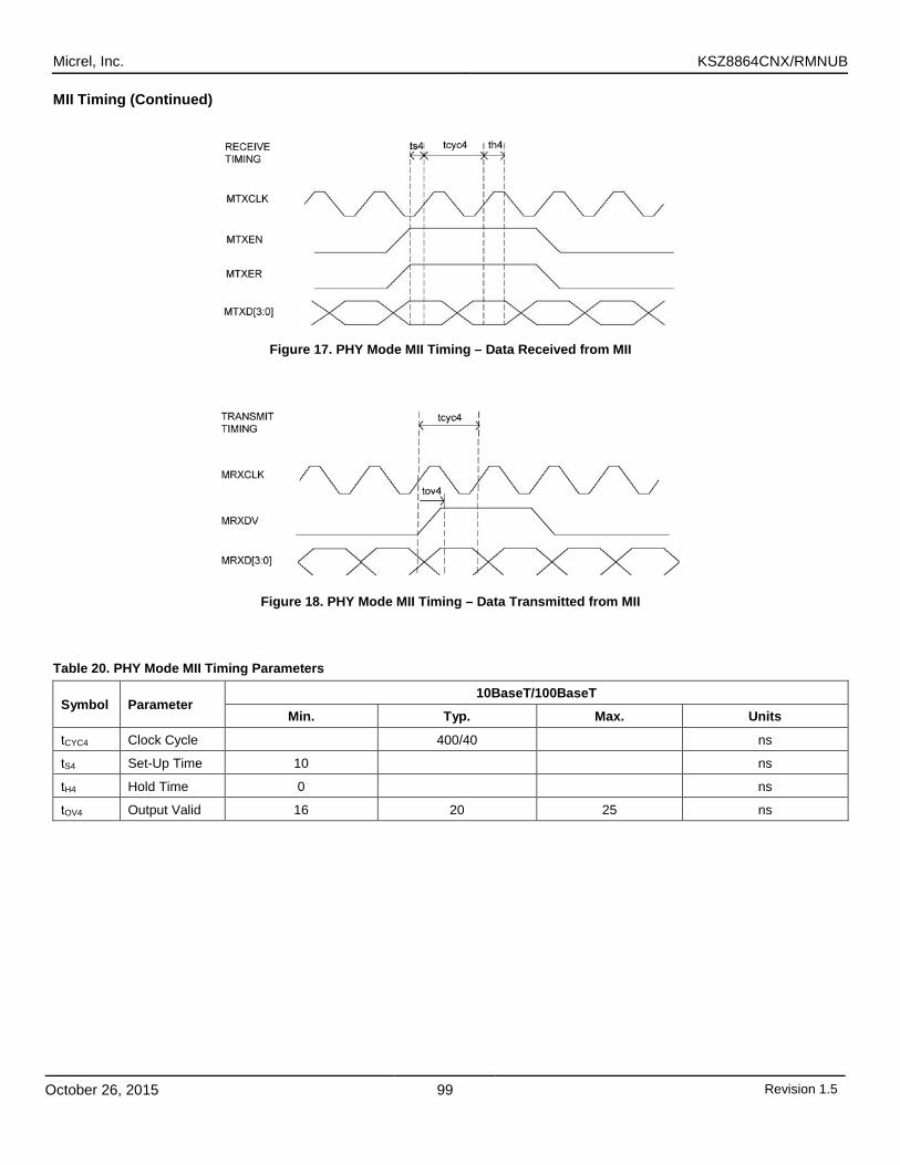
Micrel, Inc. KSZ8864CNX/RMNUB
October 26, 2015 99 Revision 1.5
MII Timing (Continued)
Figure 17. PHY Mode MII Timing – Data Received from MII
Figure 18. PHY Mode MII Timing – Data Transmitted from MII
Table 20. PHY Mode MII Timing Parameters
Symbol Parameter 10BaseT/100BaseT
Min. Typ. Max. Units
tCYC4 Clock Cycle 400/40 ns
tS4 Set-Up Time 10 ns
tH4 Hold Time 0 ns
tOV4 Output Valid 16 20 25 ns
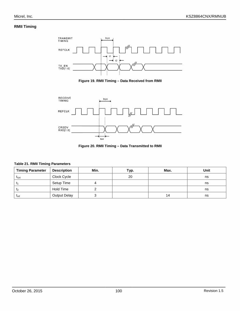
Micrel, Inc. KSZ8864CNX/RMNUB
October 26, 2015 100 Revision 1.5
RMII Timing
Figure 19. RMII Timing – Data Received from RMII
Figure 20. RMII Timing – Data Transmitted to RMII
Table 21. RMII Timing Parameters
Timing Parameter Description Min. Typ. Max. Unit
tcyc Clock Cycle 20 ns
t1 Setup Time 4 ns
t2 Hold Time 2 ns
tod Output Delay 3 14 ns
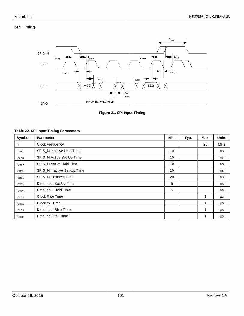
Micrel, Inc. KSZ8864CNX/RMNUB
October 26, 2015 101 Revision 1.5
SPI Timing
Figure 21. SPI Input Timing
Table 22. SPI Input Timing Parameters
Symbol Parameter Min. Typ. Max. Units
fC Clock Frequency 25 MHz
tCHSL SPIS_N Inactive Hold Time 10 ns
tSLCH SPIS_N Active Set-Up Time 10 ns
tCHSH SPIS_N Active Hold Time 10 ns
tSHCH SPIS_N Inactive Set-Up Time 10 ns
tSHSL SPIS_N Deselect Time 20 ns
tDVCH Data Input Set-Up Time 5 ns
tCHDX Data Input Hold Time 5 ns
tCLCH Clock Rise Time 1 µs
tCHCL Clock fall Time 1 µs
tDLDH Data Input Rise Time 1 µs
tDHDL Data Input fall Time 1 µs
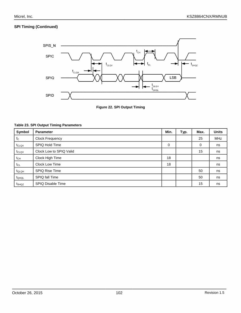
Micrel, Inc. KSZ8864CNX/RMNUB
October 26, 2015 102 Revision 1.5
SPI Timing (Continued)
Figure 22. SPI Output Timing
Table 23. SPI Output Timing Parameters
Symbol Parameter Min. Typ. Max. Units
fC Clock Frequency 25 MHz
tCLQX SPIQ Hold Time 0 0 ns
tCLQV Clock Low to SPIQ Valid 15 ns
tCH Clock High Time 18 ns
tCL Clock Low Time 18 ns
tQLQH SPIQ Rise Time 50 ns
tQHQL SPIQ fall Time 50 ns
tSHQZ SPIQ Disable Time 15 ns
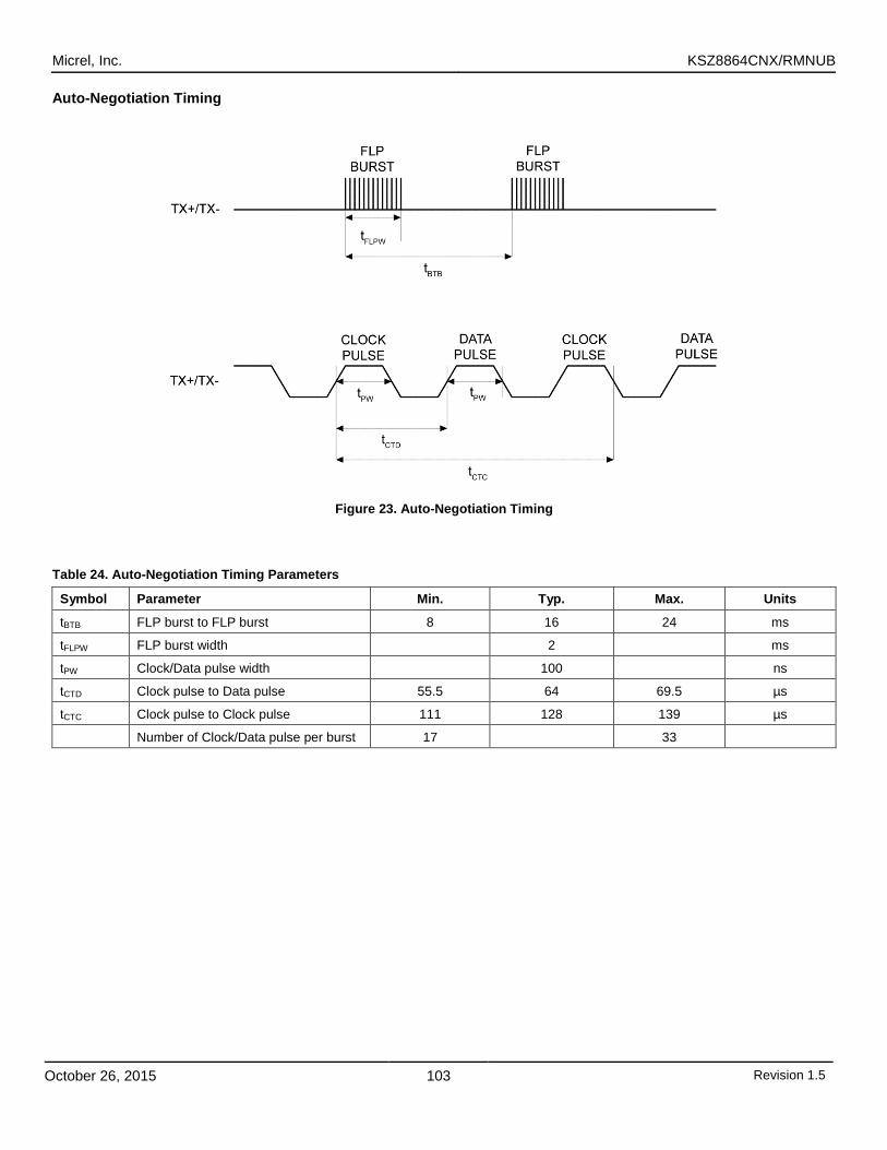
Micrel, Inc. KSZ8864CNX/RMNUB
October 26, 2015 103 Revision 1.5
Auto-Negotiation Timing
Figure 23. Auto-Negotiation Timing
Table 24. Auto-Negotiation Timing Parameters
Symbol Parameter Min. Typ. Max. Units
tBTB FLP burst to FLP burst 8 16 24 ms
tFLPW FLP burst width 2 ms
tPW Clock/Data pulse width 100 ns
tCTD Clock pulse to Data pulse 55.5 64 69.5 µs
tCTC Clock pulse to Clock pulse 111 128 139 µs
Number of Clock/Data pulse per burst 17 33
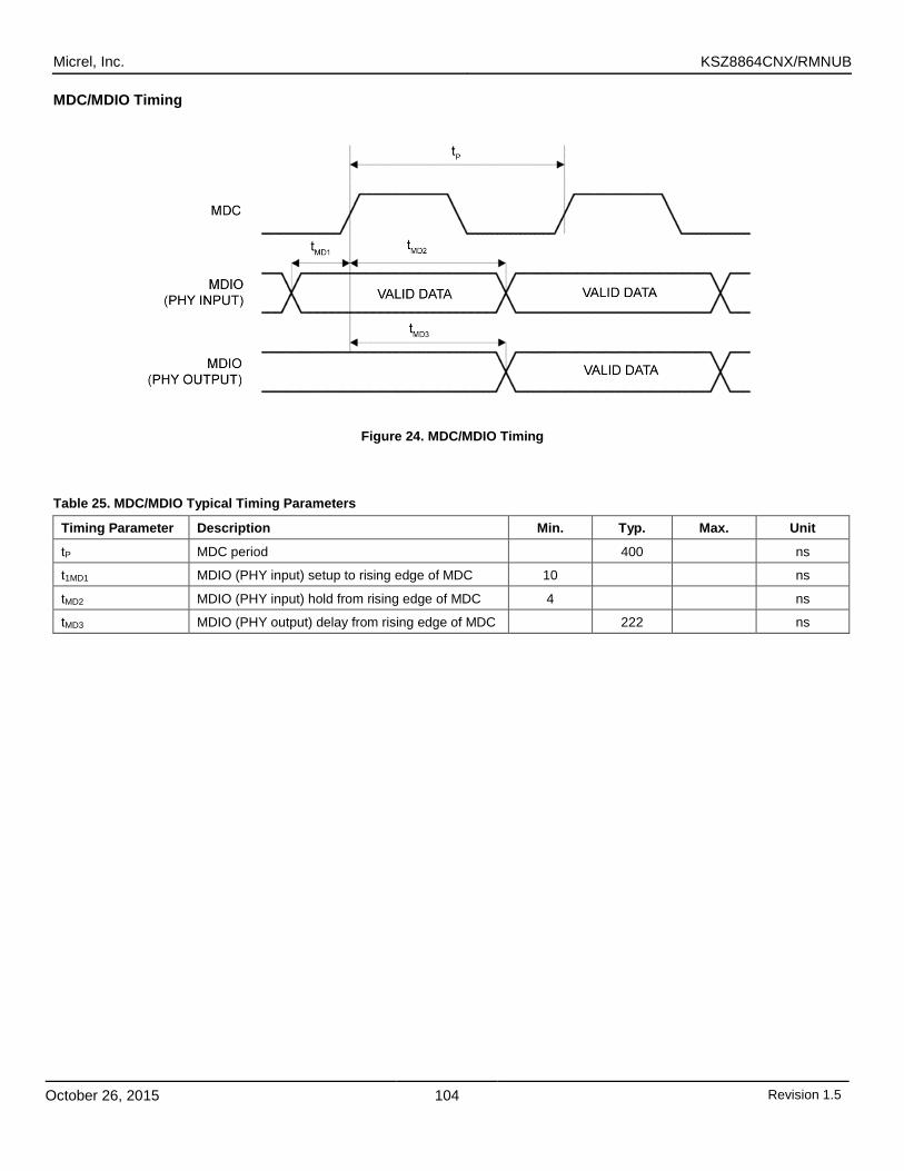
Micrel, Inc. KSZ8864CNX/RMNUB
October 26, 2015 104 Revision 1.5
MDC/MDIO Timing
Figure 24. MDC/MDIO Timing
Table 25. MDC/MDIO Typical Timing Parameters
Timing Parameter Description Min. Typ. Max. Unit
tP MDC period 400 ns
t1MD1 MDIO (PHY input) setup to rising edge of MDC 10 ns
tMD2 MDIO (PHY input) hold from rising edge of MDC 4 ns
tMD3 MDIO (PHY output) delay from rising edge of MDC 222 ns
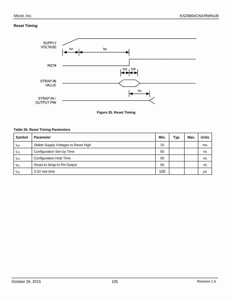
Micrel, Inc. KSZ8864CNX/RMNUB
October 26, 2015 105 Revision 1.5
Reset Timing
Figure 25. Reset Timing
Table 26. Reset Timing Parameters
Symbol Parameter Min. Typ. Max. Units
tSR Stable Supply Voltages to Reset High 10 ms
tCS Configuration Set-Up Time 50 ns
tCH Configuration Hold Time 50 ns
tRC Reset to Strap-In Pin Output 50 ns
tVR 3.3V rise time 100 µs
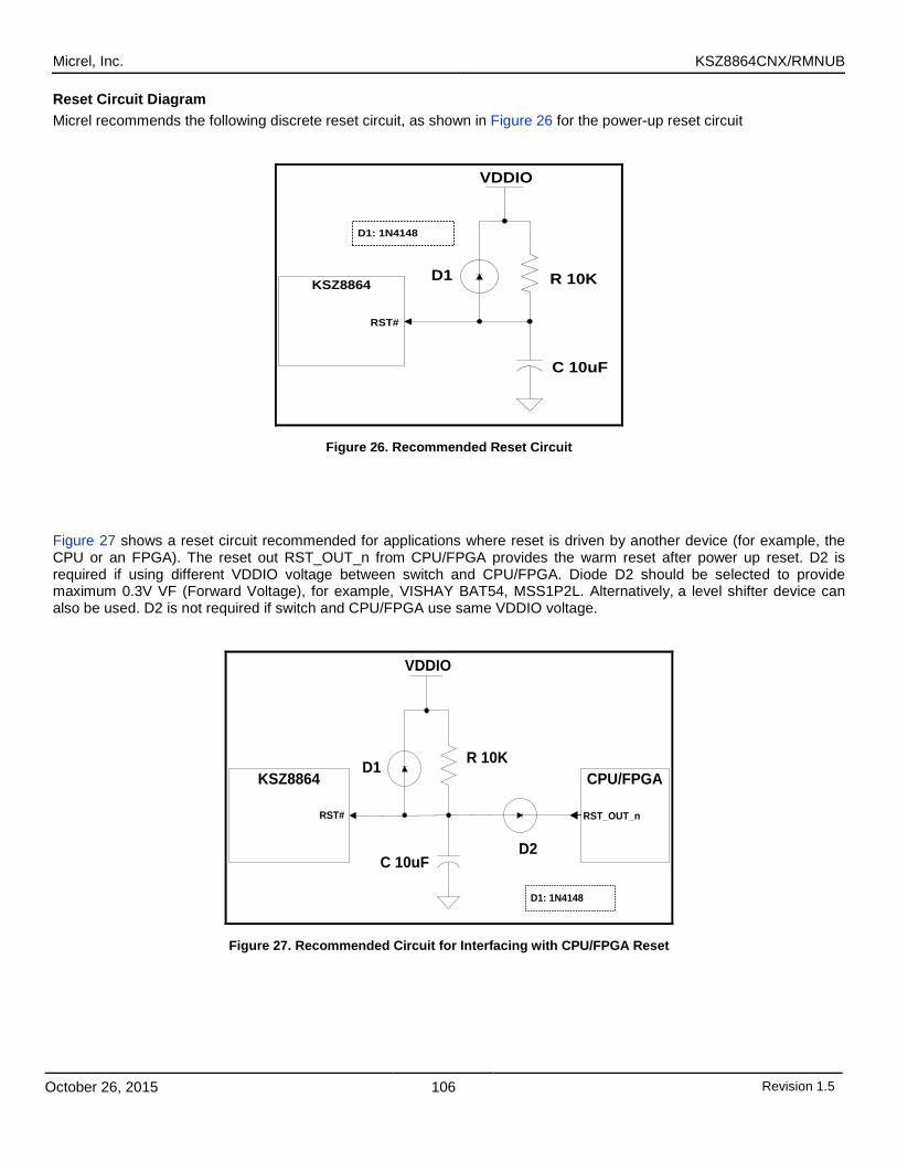
Micrel, Inc. KSZ8864CNX/RMNUB
October 26, 2015 106 Revision 1.5
Reset Circuit Diagram Micrel recommends the following discrete reset circuit, as shown in Figure 26 for the power-up reset circuit
KSZ8864
VDDIO
D1
D1: 1N4148
R 10K
C 10uF
RST#
Figure 26. Recommended Reset Circuit
Figure 27 shows a reset circuit recommended for applications where reset is driven by another device (for example, the CPU or an FPGA). The reset out RST_OUT_n from CPU/FPGA provides the warm reset after power up reset. D2 is required if using different VDDIO voltage between switch and CPU/FPGA. Diode D2 should be selected to provide maximum 0.3V VF (Forward Voltage), for example, VISHAY BAT54, MSS1P2L. Alternatively, a level shifter device can also be used. D2 is not required if switch and CPU/FPGA use same VDDIO voltage.
KSZ8864 CPU/FPGA
VDDIO
C 10uF
R 10K
RST_OUT_n
D1
D2
D1: 1N4148
RST#
Figure 27. Recommended Circuit for Interfacing with CPU/FPGA Reset
Micrel, Inc. KSZ8864CNX/RMNUB
October 26, 2015 107 Revision 1.5
Selection of Isolation Transformer(19) One simple 1:1 isolation transformer is needed at the line interface. An isolation transformer with integrated common-mode choke is recommended for exceeding FCC requirements at line side. Request to separate the center taps of RX/TX(20) at chip side. Table 30 gives recommended transformer characteristics.
Table 27. Transformer Selection Criteria
Characteristics Name Value Test Condition
Turns Ratio 1 CT : 1 CT
Open-Circuit Inductance (minimum) 350µH 100mV, 100kHz, 8mA
Insertion Loss (maximum) 1.1dB 0.1MHz to 100MHz
HIPOT (minimum) 1500VRMS
Notes: 19. The IEEE 802.3u standard for 100BASE-TX assumes a transformer loss of 0.5dB. For the transmit line transformer, insertion loss of up to 1.3dB can
be compensated by increasing the line drive current by means of reducing the ISET resistor value. 20. The center taps of RX and TX should be isolated for the low power consumption in KSZ8864CNX/RMNUB.
Selection of Transformer Vendors The following transformer vendors provide compatible magnetic parts for Micrel’s device: Table 28. Qualified Magentic Vendors
Single Port Integrated Auto MDIX
Number of Ports
Single Port Auto MDIX
Number of Ports Vendor Part Vendor Part
TDK TLA-6T718A Yes 1 Pulse H1102 Yes 1
LanKom LF-H41S Yes 1 Bel Fuse S558-5999-U7 Yes 1
Transpower HB726 Yes 1 YCL PT163020 Yes 1
Delta LF8505 Yes 1 Datatronic NT79075 Yes 1
Selection of Reference Crystal Table 29. Typical Reference Crystal Characteristics
Characteristics Value Units
Frequency 25.00000 MHz
Frequency Tolerance (maximum) ≤ ±50 ppm
Load Capacitance (maximum) 27 pF
Series Resistance (ESR) 40 Ω
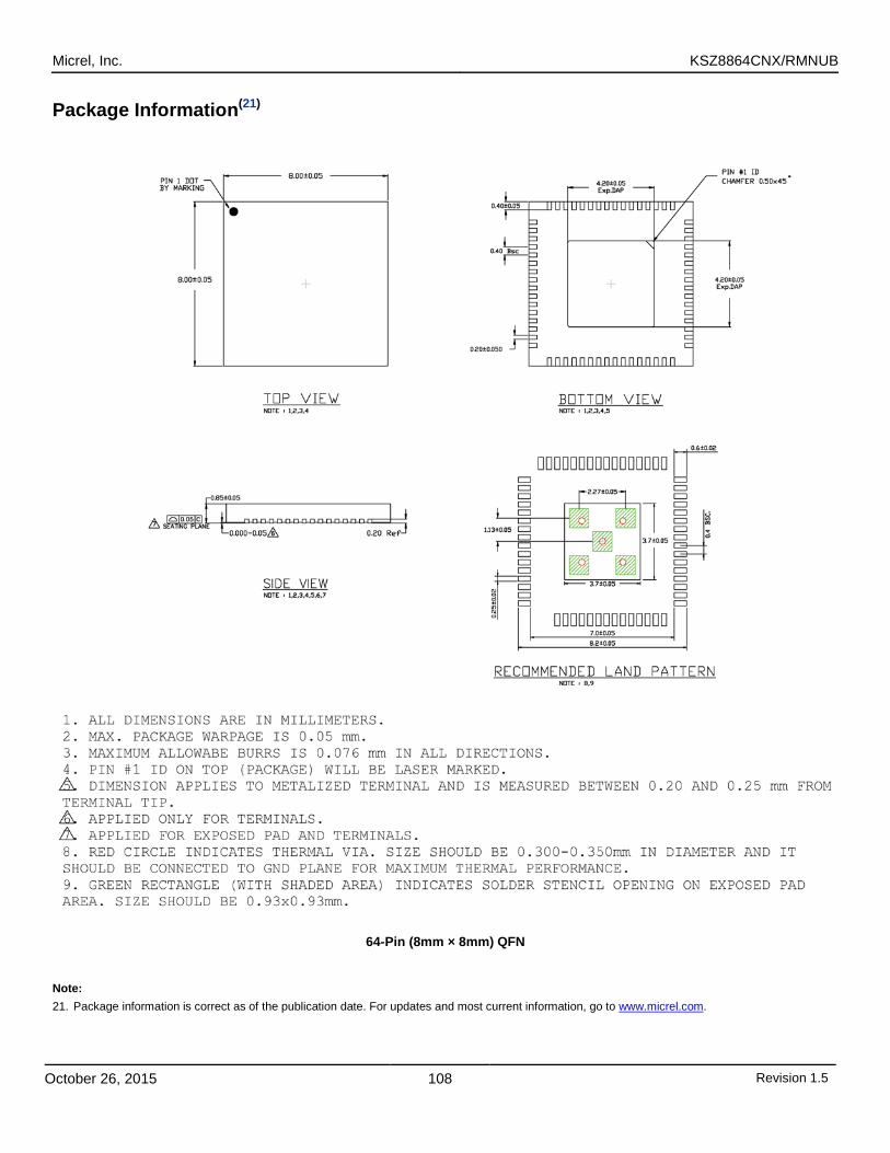
Micrel, Inc. KSZ8864CNX/RMNUB
October 26, 2015 108 Revision 1.5
Package Information(21)
64-Pin (8mm × 8mm) QFN
Note: 21. Package information is correct as of the publication date. For updates and most current information, go to www.micrel.com.

Micrel, Inc. KSZ8864CNX/RMNUB
October 26, 2015 109 Revision 1.5
MICREL, INC. 2180 FORTUNE DRIVE SAN JOSE, CA 95131 USA TEL +1 (408) 944-0800 FAX +1 (408) 474-1000 WEB http://www.micrel.com
Micrel, Inc. is a leading global manufacturer of IC solutions for the worldwide high-performance linear and power, LAN, and timing & communications markets. The Company’s products include advanced mixed-signal, analog & power semiconductors; high-performance communication, clock management, MEMs-based clock oscillators & crystal-less clock generators, Ethernet switches, and physical layer transceiver ICs. Company customers include leading manufacturers of enterprise, consumer, industrial, mobile, telecommunications, automotive, and computer products. Corporation headquarters and state-of-the-art wafer fabrication facilities are located in San Jose, CA, with regional sales and support offices and advanced technology design centers situated throughout the Americas, Europe, and Asia. Additionally, the Company maintains an extensive network of distributors and reps worldwide. Micrel makes no representations or warranties with respect to the accuracy or completeness of the information furnished in this datasheet. This information is not intended as a warranty and Micrel does not assume responsibility for its use. Micrel reserves the right to change circuitry, specifications and descriptions at any time without notice. No license, whether express, implied, arising by estoppel or otherwise, to any intellectual property rights is granted by this document. Except as provided in Micrel’s terms and conditions of sale for such products, Micrel assumes no liability whatsoever, and Micrel disclaims any express or implied warranty relating to the sale and/or use of Micrel products including liability or warranties relating to fitness for a particular purpose, merchantability, or infringement of any patent, copyright, or other intellectual property right. Micrel Products are not designed or authorized for use as components in life support appliances, devices or systems where malfunction of a product can reasonably be expected to result in personal injury. Life support devices or systems are devices or systems that (a) are intended for surgical implant into the body or (b) support or sustain life, and whose failure to perform can be reasonably expected to result in a significant injury to the user. A Purchaser’s use or sale of Micrel Products for use in life support appliances, devices or systems is a Purchaser’s own risk and Purchaser agrees to fully indemnify Micrel for any damages resulting from such use or sale.
© 2014 Micrel, Incorporated.