Embed Size (px)
Citation preview

Integrated Power Management
Platforms:
What is new and what is still missing
Shye Shapira Director of RD
Power Management Platforms
TowerJazz
ASRC Seminar May 2013

Digital Chip – (Managing Power at V~1V,I~1-100 mA)
Small, Medium Portable System PDA, Cell phone,
Laptop. LED TV screen Motor Drives, Motherboard
Power Management, Audio Amplifiers (Vdd~5-100V,
I~ mA-20A)
Off Grid Devices : Power Adapter, LED Lamp
(V~700V I~ 10mA- 1A)
Large Portable System (Ships, Drilling Towers,
Airplanes, Spaceships )( V~1000-10000v, I -100 -
1000 A)
Large Static system -> US national power Grid (Smart
Grid Programs) (V- 100kV?)
The (Electrical) Power Management Map
2
Integrated Power Management
Drivers for Integration:
Portability
Efficient Use of Energy (Grid Voltage, Lighting)

Integrated Power Management Application
Space DC DC Converter (“Boost Buck” Convertors Std Alone, Digital Cameras)
LED Drivers.
Motor Drivers.
AC adapters. (Brick replacement )
– Voltages 400 to 600V
– Lighting
Future Automotive 48V
Line Drivers
Audio Amplifiers. Low Ron and low noise.
Power over Ethernet
RF Power Amplifiers

Step-Down (“Buck”) DC-DC Converter
Switching input to the
low-pass filter.
Ideal Efficiency 100%
4
Vo=Vin* Ton/(Ton+Toff)
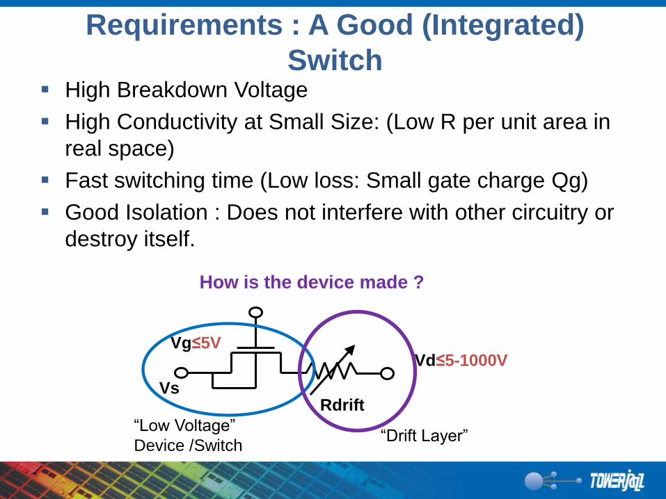
Requirements : A Good (Integrated)
Switch High Breakdown Voltage
High Conductivity at Small Size: (Low R per unit area in
real space)
Fast switching time (Low loss: Small gate charge Qg)
Good Isolation : Does not interfere with other circuitry or
destroy itself.
Vs
Vd≤5-1000V Vg≤5V
Rdrift
“Low Voltage”
Device /Switch “Drift Layer”
How is the device made ?
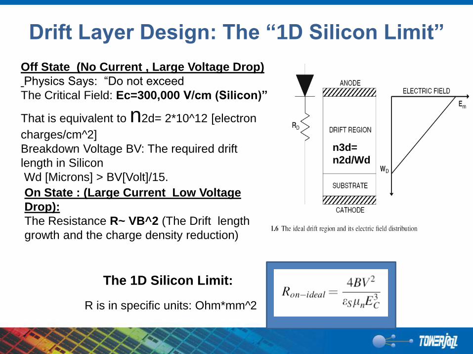
Drift Layer Design: The “1D Silicon Limit”
Diagram from Baliga Fundamentals of Power Semiconductor Devices
The 1D Silicon Limit:
R is in specific units: Ohm*mm^2
Off State (No Current , Large Voltage Drop)
Physics Says: “Do not exceed
The Critical Field: Ec=300,000 V/cm (Silicon)”
That is equivalent to n2d= 2*10^12 [electron
charges/cm^2]
Breakdown Voltage BV: The required drift
length in Silicon
Wd [Microns] > BV[Volt]/15.
On State : (Large Current Low Voltage
Drop):
The Resistance R~ VB^2 (The Drift length
growth and the charge density reduction)
n3d=
n2d/Wd

Going 2D : “RESURF” (Reduced Surface
Field)
7
Appels (79)
Ludikhuize (2000).
Concept :
1d:dEx/dx= nq/epsilon: E grows
continuously at constant drift layer
density.
2d: dEx/dx+dEy/dy= nq/epsilon.
if dEx/dx>>0 We can have dEy/dy=0
The growth of Ey is suppressed
->
High voltages sustained with a High Drift
Density (ndr~ 2*10^12 cm^-2)
Hence high conductance (~2.1
Kohms/Square).
Nepi
Psub
P+ N+
Vdd
n3d=
n2d/Wd
Y
X
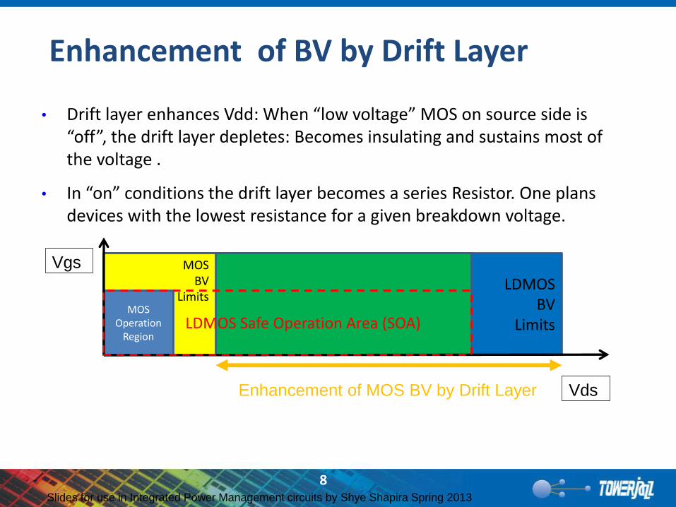
Enhancement of BV by Drift Layer
• Drift layer enhances Vdd: When “low voltage” MOS on source side is “off”, the drift layer depletes: Becomes insulating and sustains most of the voltage .
• In “on” conditions the drift layer becomes a series Resistor. One plans devices with the lowest resistance for a given breakdown voltage.
8 Slides for use in Integrated Power Management circuits by Shye Shapira Spring 2013
LDMOS BV
Limits
MOS BV
Limits MOS
Operation Region
Vgs
Vds
LDMOS Safe Operation Area (SOA)
Enhancement of MOS BV by Drift Layer

9
Rdson Reduction
STI Length is scaled to
achieve Rdson Bvdss
scalable tradeoff.
STI Replaced by LOCOS
To Achieve a better Tradeoff
Rdson Bvdss
N+
P-
Poly
STI
Slides for use in Integrated Power Management circuits by Shye Shapira Spring 2013
Self aligned Body implant
reduces footprint
Ehnanced Ndrift
doping Reduces
Rdson
Ehnanced
Pdoping

Specific Rdson Reduction:
Integrated Vertical Device
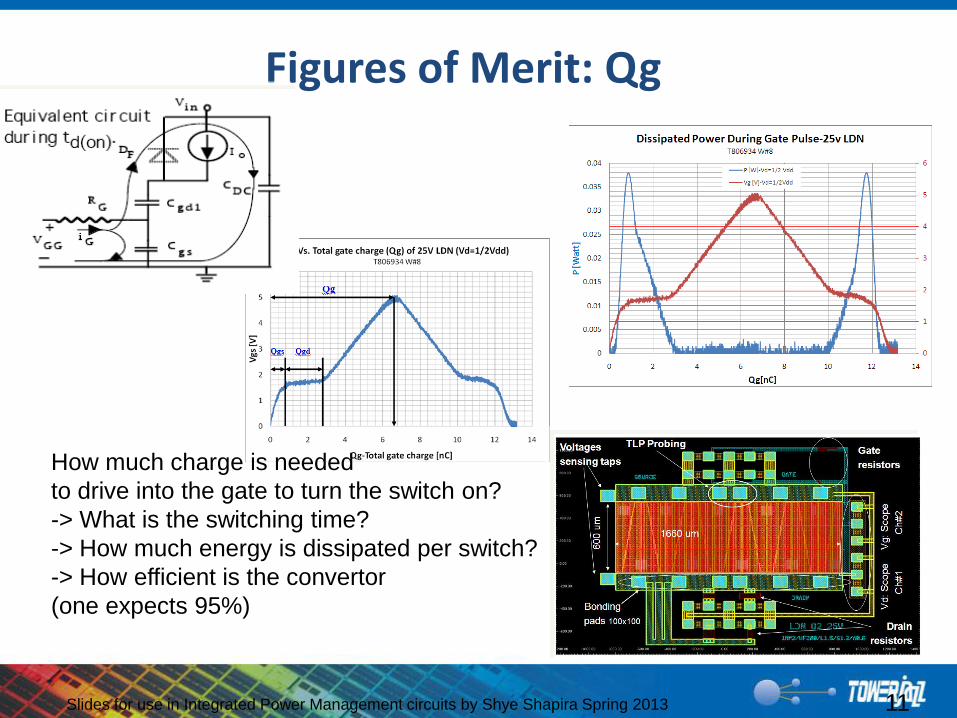
Figures of Merit: Qg
How much charge is needed
to drive into the gate to turn the switch on?
-> What is the switching time?
-> How much energy is dissipated per switch?
-> How efficient is the convertor
(one expects 95%)
Slides for use in Integrated Power Management circuits by Shye Shapira Spring 2013 11

Integrated Power Management Platform
Deep Nwell
HV Pwell (PHV)
Poly
P+
M1
Emitter
M1
Base
Poly
P+ N+
M1
Base
N+ N+
M1
Collector
M1
Collector
HV VNPN Biploar LD pMOS
Deep Nwell
P- Drain (PHV)
M1
Drain
M1
Gate
M1
Source
& Body
P+ P+
Poly
STI
0V <= Vg <= 5V; 0V <= Vd <= 25V
Self Aligned LD nMOS
Deep Nwell
P-Body
M1
Drain
M1
Gate
M1
Source
& Body
N+P+ N+
Poly
STI
0V <= Vg <= 5V; 0V <= Vd <= 25V
1.8V pMOS 5V pMOS 5V nMOS1.8V nMOS
3.3V Nwell
M1M1
P+
Poly
P+
M1
3.3V Pwell
N+
Poly
N+
M1M1 M1
1.8V Pwell
N+
Poly
N+
M1M1 M1
1.8V Nwell
M1M1
P+
Poly
P+
M1
Vg<=1.8V; Vd<=1.8V Vg<=5V; Vd<=5V
Standard
Platform: Less than
60% of chip
size : Total
Area
determined
by technology
node (“All”
Tools )
High Voltage
Drivers: Over
60% of chip
size : Total
Area scales
with Rdson
(Device
Engineering,
few Tools)
High Voltage Devices Embedded in the Standard Platform

0
20
40
60
80
100
0 20 40 60 80 100
Rd
so
n (
mo
hm
-mm
2)
BVdss [V]
Rdson vs. BVdss of nLDMOS transistor
TowerJazz Gen1
TowerJazz Gen1
TowerJazz Gen2
TowerJazz Gen3
TowerJazz Gen4 (in Dev)
2012 Enhancements
Engineering Solution

High Side and Low Side Injection
14
Deep Nwell (WTN)
P-Body
M1
Drain
M1
Gate
M1
Source
& Body
N+P+
Poly
STI N+
Shallow Buried Layer
Source Isolation Deep Buried Layer Drain
and Source Isolation
High Side Injection:
•Holes from Body to Drain Well
Diffuse to Substrate.
•Effect:
•High substrate currents
•Large Dissipation (Voltage
Drop Vdd), Device Destruction
•Mitigation : Shallow Buried
layer
Low side Side Injection:
Electrons Injected From Drain To
Substrate
Effect: Large Substrate Current
Mitigation: P+ substrate
Isolated Drain

700 V Lighting and off Grid Applications
• Ac Dc Convertors (240v ac to xV Dc) • Lighting : Street / Indoor

700V Double Resurf NLDMOS
Used in 100s V devices : Double Resurf: Drift layer between two P-layers.
Field goes from +Ec to –Ec. Density of drift layer and hence conductivity
doubles.

RdsOn of 700V Devices
5
7
9
11
13
15
17
19
21
400 500 600 700 800 900
Rd
sOn
[Ω
*mm
²]
BVdss [V]
RdsOn Vs Breakdown Voltage

drain
source/body
(psub) gate
NBL (high
voltage region)
psub
dnblpsub_hs
18 /
Vdc
High Side
Low Side
Vh
Vo
Vs
External
Devices
load
LDMOS
Interconnection
Vdd
Bootstrap diode
High Side Circuits
R
700V High Side Block Diagram
Level
Shifter
Floating
NMOS
TowerJazz Confidential

700VHigh Side /Low Side Platforms
Low side platforms include these

Future
Technologies

Future Technologies: Integrating
Passives on PMIC
21
PMIC Chip
Inclusion in chip/package stage rather than board in a simple procedure:
1. Allow chip design company more flexibility and “food chain space” in designing a system
with inductor PDK
1. Reduce board size
Board

Future Technologies : Full Integration of
Passives for Power Management ICs. Capacitance limits:
Needed : 1uF/mm^2@5-50V
Have :
CMOS: 5nF-10 nF/mm^2 @ (BV=3-6V )
DRAM : ~ 100 nF/mm^2 @ (BV=3-6V )
Inductance Limits :
Needed :
1microHenry /mm^2 @ 1A (f~0.5-1 mHZ), Low ESR
Have: 10s nHenry @ GhZ
Trends to achieve integration:
Performance at Higher frequencies (Better Performance)
High Dielectric Constant
Higher effective Surface
Solution must be cost effective

Integrating Inductors on PMIC:
Implementation Example
June 12, 2011 TowerJazz Confidential
23
2mm
Typical Power Chip
Size and Specs:
L=0.5-1uH
I =1A
Work with prof. Yael Nemirovsky at Technion
See Svitliza 2011 (ieeexplore)

TowerJazz Confidential
Future Technologies : More Efficient
Semiconductor Platforms.
Efficiency scales with Qg*Rdson
Losses: Conduction/switching (capacitive and
Conduction)
GaN: Large Bandgap ,High Mu, - Low
Qg*Rdson
Medium Heat Conductivity
Breakthrough : GaN on Silicon
SiC: Large Bandgap High Heat Conductivity

n-GaN
AlXGa1-xN
Ohmic Drain
Contact
GaN HEMTs for Power Electronics
SiC or Si <111> Substrate
AlN Buffer
Schottky Gate
Contact
2DEG
Ohmic Source
Contact Dielectric
VDD V>0 (enhancement mode)
V=0 (depletion mode)
• Basic GaN HEMT structure with channel turned on.
• Typical VT is about 1.5V for enhancement mode devices
Further Reading
TowerJazz Confidential
Technology : www.towerjazz.com
Technical papers examples
(ieeexplore look up author et al and Jazz/ Tower / TowerJazz):
Z. Lee , 2007,Klein , 2008, Mayzeles 2008, Berkovitch 2010, Levin 2011,Kanawati 2011.
Svitliza 2011. Ophir-Arad 2012 Vardy 2012 Shapira 2012.
Review
Course 046235 Integrated Power Management Platforms-Technion
Fundamentals of Power Semiconductor Devices By Baliga, B. Jayant 2008
Technology:
acrc.ee.technion.ac.il/.../Shapira%20Power%20Technology%20ACRC_JULY_2010.p
df
Industry :
Integrated Power Management Platforms: The Entry of Fabless Design Houses to Power
Management System Design(GSA Forum June 2010)
אלון אייל , Tapeout LED ו AC DC פלטפורמות ניהול הספק לשימושי
שי שפירא Tapeout פלטפורמות ניהול הספק להתקנים ניידים והתקני תאורה

Thank You

![What Influences Choice of Business-to-Business Connectivity Platforms? · 2018-09-27 · Compared to the traditional, linear, value-chain-based “pipeline busi-nesses” [48], platforms](https://img.pdfslide.net/doc/110x75/5f2e1a1b69e2363192342667/what-influences-choice-of-business-to-business-connectivity-platforms-2018-09-27.jpg)


![[CCDD2013w] What to make of today’s "smart" platforms by 蔡亦恒](https://img.pdfslide.net/doc/110x75/55ab1e661a28ab1a678b463f/ccdd2013w-what-to-make-of-todays-smart-platforms-by-.jpg)