Embed Size (px)
Citation preview
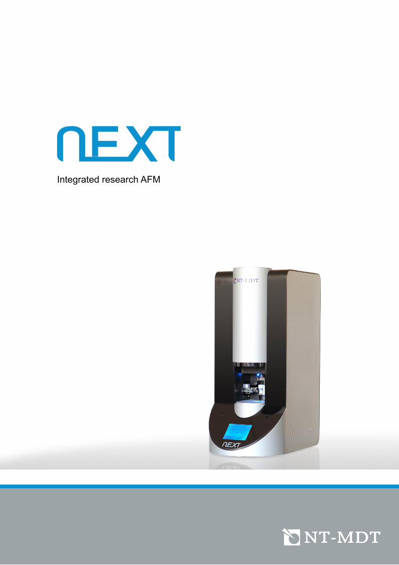
Integrated research AFM

2
High resolution imagingNEXT has 25 fm/√Hz optical deflection noise level. This level of performance is driving advanced high-resolution imaging capabili-ties. Meticulously elegant NEXT mechanical design, together with the low noise level of the closed loop piezoscanner, thermally stabilized acoustic enclosure and vibration tolerant system makes high resolu-tion imaging a routine procedure.
Advanced AFM and STM characterization techniquesTwo automatically interchangeable measuring heads (AFM and STM) are integrated into the NEXT. Driven by the new digital PX Ultra con-troller the NEXT delivers the broadest range of AFM and STM tech-niques —for sample topography, electrical, magnetic and nanome-chanical properties characterization. Multifrequency AFM techniques dramatically increase the amount of information acquired from single experiment.
Exceptional level of automation for both beginners and expertsNEXT provides motorized sample positioning and integrated high resolution optical microscope positioning, motorized continuous zoom and focusing of the optical microscope. But AFM automation is more than motorization. The Smart automatic alignment algorithm provides fast laser-cantilever-photodiode optical chain alignment turning this routine procedure into single click 10 second operation. Powerful soft-ware automation features drive AFM productivity to a new level.
AFM measuring head
STM measuring head
5 years ago NT-MDT introduced the first fully automated desktop AFM. We are now proud to introduce the new generation NEXT product.NEXT is the perfect integration of automation expertise and a company that for the last 22 years has provided high-resolution, research-performance AFM instruments

3
High Resolution Imaging
25 fm/√Hz optical beam deflection (OBD) sensor noiseLow OBD sensor noise is essential for high-resolution imaging. 25 fm/√Hz noise level of NEXT OBD sensor allows precise control and minimization of the forces acting between probe and sample, making it possible to operate with sub-nanometer or even sub-angstrom oscillation amplitudes of the cantilever. Ultimate resolution amplitude modulation AFM imaging of wide variety of samples both in liquid and in air is routinely available. Including visualization of individual polymer chains in soft specimens like PTFE thin films.
Gentle approach algorithm Probe sharpness is critical for acquiring perfect AFM images, but sometimes the probe might be damaged during the approach procedure even before beginning the experiment. NT-MDT has developed a phase sensitive algorithm that guaranties gentle probe approach.
High stability and powerful vibration and acoustic insulationNEXT enclosure provides acoustic insulation and active thermal stabilization of the microscope decreasing thermal drift down to the level of ~10 nm/hour. Integrated active vibration insulation system serves powerful protection form external mechanical noise.
Paraffin wax topography images after probe approach: (a) – phase control, (b) – amplitude control. 6×6 mm scan
Mica atomic lattice resolution, LFM mode. Scan size 6×6 nm
DNA on mica surface, AM-AFM mode. Scan size 1×1 mm
Calcite atomic resolution, AM-AFM mode in liqud. Scan size 6×6 nm
Height image of the ab plane of TTF-TCNQ crystal. AM-AFM.
Scan size 9×9 nm
HOPG atomic lattice resolution,STM. Scan size 2.1×2.1 nm
Although the first AFM was introduced more than 25 years ago, high resolution imaging is still driving strong competition amongst AFM manufacturers. NEXT low noise performance makes high resolution imaging a routine procedure
(a) (b)

4
Advanced characterization techniques
Phase image, 2nd pass.Double-pass EFM
Topography
SDRAM structure, AM-KPFM mode: (a) topography, (b) surface potential. Scan size 40×40 mm
Multifrequency drive and Phase imagingMesomorphic Poly(diethyl siloxane) on a Si substrate. Addi-tional sample details are seen in the second flexural image. 20×20 mm scans. Phase image, 1st flexural mode (a), phase image, 2nd flexural mode (b).
Surface potential.Single-pass PM-KPFM
Amplitude, 2nd pass.Double-pass EFM
TGS crystal, PFM mode: (a) topography, (b) VPFM phase. Scan size 40×40 mm
(a) (b)
Modern AFM instruments are much more than just a tool for topography imaging. Coupled with the PX Ultra controller the NEXT realizes the largest suite of multifrequency AFM techniques
P3HT/PCBM blend film deposited on ITO glass. Scan size 600×600 nm
(a) (b) (a) (b)
NEXT multifrequency configuration schematics
AC Deflection
Laser
Photo
dete
cto
r
Amplitude
Phase
X componentA Cos ( )�m
Sample
Cantilever
Tip Bias Voltage
PiezoShaker �m
�m
Surface Potential
Amplitude/Phase
Amplitude/Phase
Amplitude/Phase
�e
Digital Lock-ins
Lock-in 3�e
Lock-in 42�e
Lock-in 53�e
Lock-in 1�m
Lock-in 2�e
AC Drive
U Drive + DC ServoAC
Phase Shifter
Phase Shifter
Z Servo
KPFM Servo
U DriveAC
�e
AM-AM
AM-PM
Frequensy Servo

5
Multifrequency EFM and KPFM
Height
Amplitude (AM) and phase modulation (PM) single pass EFM and KPFMFlexible and easy configuration of feedback loops allows simultaneous multifrequency measurements using up to 5 lock-ins (2 high frequency, 3 low frequency) for operation in both AM and PM electrical AFM modes. This gives the widest range of sample measurement capabilities, from single macromolecules to photovoltaic structures.
Pre-defined software settings Nova PX software contains pre-defined settings for fast configuration of the NEXT operation — in single pass AM/PM KPFM, single pass AM/PM EFM, dual pass EFM, MFM and KPFM modes.
Flexibility to match the correct technique to the sampleAlong with fast configuration of predefined modes Nova PX software allows researchers to have unlimited experiment flexibility.
Multifrequency PFM
Piezoresponce Force Microscopy (PFM) is attracting a strong growing interest led by applications of piezo materials and by research of electromechanical properties of biological systems. Along with domain structure, a number of specific ferroelectric properties (coercive field, residual polarization, etc.) can be revealed using Switching Spectroscopy. The NEXT guarantees high quality of PFM scans by eliminating cross-talk interfer-ence of the normal and the lateral components of the cantilever deflection signal.
VPFM, Amplitude VPFM, Phase
Height Potential, PM-KPFM Potential, AM-KPFM
Surface Potential
dC/dV contrast
dC/dZ contrast
0 200 400 600
200
600
nm
mV
0 200 400 600 nm
mV
02
00
40
0
+30V-30V 0V
Surface Potential, AM
Surface Potential, PM
Switching Spectroscopy: 1 - amplitude, 2 - phase, 3 - piezoresponce
F14H20 self-assembly on Si surface. Scan size 1x1 mm
BFO sample with a central 2 mm area polarized by a scanning probe.
+30V-30V 0V+30V-30V 0V
3 mm 3 mm 3 mm 4 mm
6
PS Elastic Modulus measuredon the basis of the DFL curves(solid lines) and FvH curves (dashed lines) obtained on PS surface. DvZ, FvH curves: red – loading, blue – unloading traces
Nanomechanics - Nanoindentation
Zr ceramics. Topography (а) and elastic modulus map (b), 1×1 mm
AFM image of indentation imprint, 18×18 mm
AFM image of scratches, 5×5 mm
Indentor: diamond pyramid of Berkovich type
-600 -200 0 200
0
2
4
6
PDMS130
PDMS60
PDMS8
Z, nm
DFL, nm
Z, nm
DFL, nm
-600 -200 0 200
0
2
4
6
0
200
600
Forse, nN
1000
Polymer Material
Elastic ModulusMacro AFM
LDPE 152 - 290 MPa 204 MPaPC 1.79 - 3.24 GPa 2.30 GPaSiLKTM 2.45 GPa 2.25 GPa
Nanomechanical Studies in Contact ModeAFM based nanoindentation provides:Acquire images of topography, phase, electrical properties of the sample surface prior to indentationAcquire force-displacement curves on nanoscale sample regions. Perform nano-indentation or scratch-testing with further scanning of the indented regionAnalyze plastic deformation or viscoelastic recovery
Work of Adhesion measured on the basis of the DFL curves on filmsof PDMS8, PDMS60 and PDMS130. DvZ curves: red – loading, blue – unloading traces
Polymer Material
Work of AdhesionMacro AFM
PDMS-8 49 32PDMS-60 58 52.2PDMS-130 47 - 58 42.1
The nanosclerometry moduleThe NEXT diamond probe nanoindentor measuring head is optimized for hardsamples (1-1000 GPa). It allows acquiring sample topography, distribution ofmechanical properties over the sample (measuring of elasticity modulus) andis able to perform micro-, nanoindentation or scratch-testing with furtherscanning of the indented region.
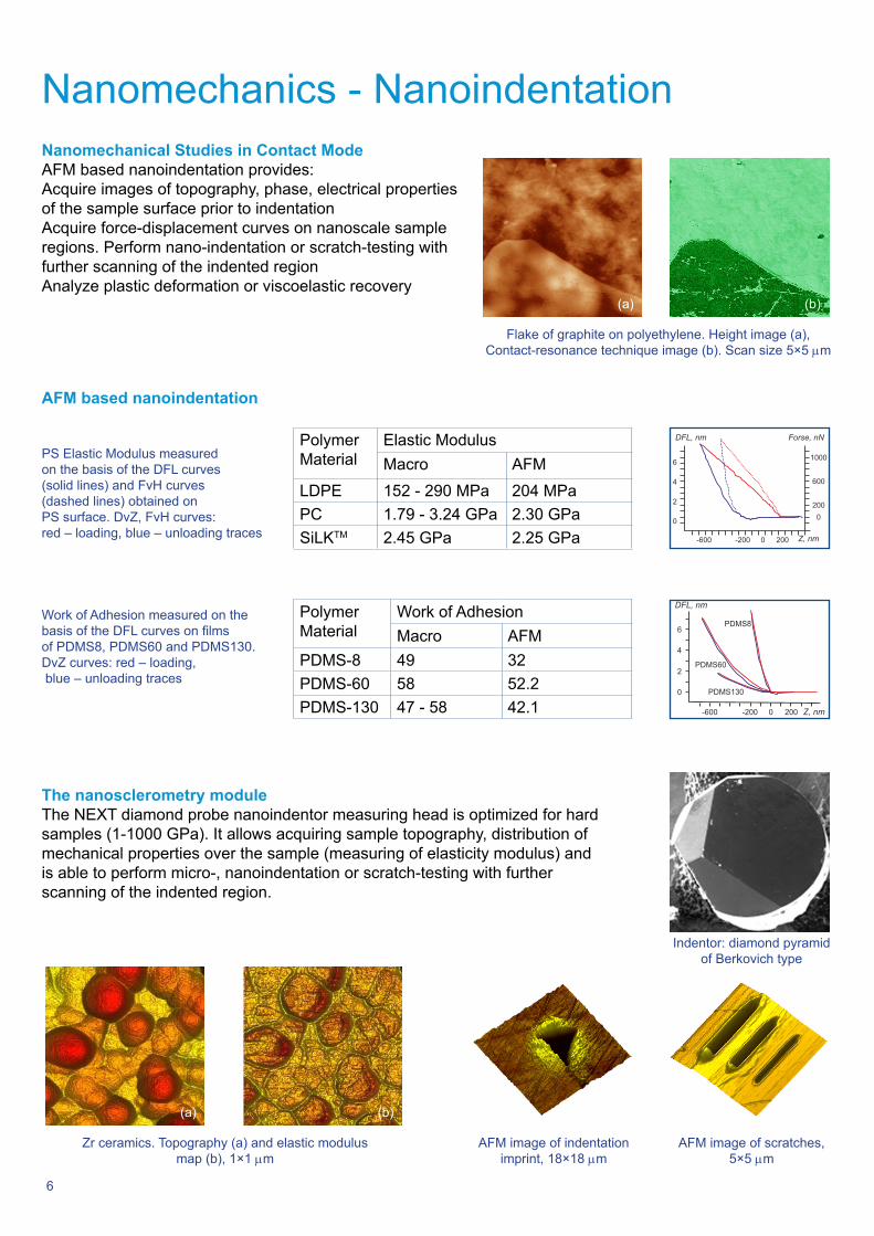
Flake of graphite on polyethylene. Height image (a), Contact-resonance technique image (b). Scan size 5×5 mm
AFM based nanoindentation
(a) (b)
(a) (b)

7
10 sec
Laser – cantilever – photodiode autoalignment within 10 seconds
Point-and-click motorized precise sample positioning
Exceptional Level of Automation
Panoramic optical view, Multiscan and ScanStitch
NEXT is a fully automated AFM. Exceptional level of automation makes routine procedures much faster and easier. Powerful software algorithms provide high experiment productivity for both beginners and experts
Precise sample positioning in the NEXT is done by motorized XY sample stage. It is veryconvenient to just select an area of interestdirectly on the optical image. The NEXT willautomatically move it to cantilever and beginscanning.
A 2 μm resolution optical microscope is integrated into the NEXT. The optical microscope is placed on5×5 mm XY precise motorized stage. Both optics and sample stages can move independently relative tothe cantilever. Nova PX software provides many convenient features based on these properties of theNEXT hardware.Panoramic optical view allows collection of high resolution, large scale images of the sample and thenoperation with this data as the same as one operates with interactive maps.Multiscan and ScanStitch provides easy acquisition of scans with ~ mm scan size within a reasonable timeand overlay AFM scans with the optical image
A single click on the cantilever in the optical image is enough. NEXT will automatically complete the alignment in 10 seconds. This algorithm works independently of the optical zoom value and optical field of view position relative to the cantilever. Actually it takes about 30% less time than it takes to read this paragraph.
Panoramic 6×6 mm optical image of IC stitched from a number of smaller images (central green restangle).Picture file contains 50 MP (2 mm optical resolution).
3×3 AFM multiscan (consist of stitched 95x95 mmscans) overlayed with optical image
10 sec

8
SpecificationsMeasuring heads• Built-in, with the automatically
interchangeable: AFM and STM• Optional: for measurement in liquid and
nanoindentation.• OBD system, with automated alignment and
targeting
Sample• Dimensions: up to 20/10 mm in diameter/
height• Sample weight: up to 40 g• Heating: from RT to 150 °С
Scanning system• Scanning type: by sample• Range: 100 × 100 × 10 mm (CL)
3 × 3 × 2 mm in HR mode
Resolution• Noise XY: not more than 0.3 nm (with closed
loop sensors)• Noise Z (RMS, 10-1000 Hz bandwidth): 15 pm
(typical)
Sample positioning system• Movement: automated, binded with the
positioning system of the videomicroscope• Range, XY: 5 × 5 mm• Minimal step: 0.3 mm
Video monitoring system• Resolution: 2 mm• Focusing: motorized• Zoom: continuous, motorized
Nanosclerometry• Hardness: 1...80 GPa• Elasticity modulus: 1...1000 GPa
Size and weight• Size: 470 × 210 × 260 mm• Weight: 25 kg
ModesContact AFM• Topography• Feedback • Lateral Force (LFM)• Force Modulation (FMM)Amplitude modulation AFM • Topography• Phase • Feedback AFM spectroscopy • Force-distance • Amplitude-distance • Phase-distance • I(V)Raster Spring Imaging Spreading Resistance ImagingMagnetic Force Microscopy • Two-pass DC/AC• Lift DC/ACElectrostatic Force Microscopy• Single-pass, Two-pass • Amplitude Modulation • Frequency Modulation • dC/dZ imaging • dC/dV imagingKelvin Probe Force Microscopy • Single-pass, Two-pass• Amplitude Modulation • Phase Modulation PFM & Switching SpectroscopyNanolithography• Voltage• Current• ForceNanosclerometry• Elastic modulus mapping • Scratch hardness • Nanoindentation STM
Distributors world-wideNT-MDT Co,Building 100, Zelenograd, Moscow, RussiaTel.: +7 (499) 735 7777Fax.: +7 (499) 735 6410E-mail: [email protected], www.ntmdt-tips.comINTEGRATED SOLUTION FOR NANOTECHNOLOGY


![Composites Science and Technology - ntmdt-si.com · 2015. 1. 20. · 110 years [1]. The discovery of graphene [2,3], a light, stiff material with the unique conductive properties,](https://img.pdfslide.net/doc/110x75/6113fb3b87358831d80094a3/composites-science-and-technology-ntmdt-sicom-2015-1-20-110-years-1-the.jpg)