Embed Size (px)
Citation preview
ieee transactions on ultrasonics, ferroelectrics, and frequency control, vol. 55, no. 2, february 2008 327
Integration of 2D CMUT Arrays withFront-End Electronics for Volumetric
Ultrasound ImagingIra O. Wygant, Student Member, IEEE, Xuefeng Zhuang, Student Member, IEEE,
David T. Yeh, Student Member, IEEE, Omer Oralkan, Member, IEEE, A. Sanli Ergun, Member, IEEE,Mustafa Karaman, Member, IEEE, and Butrus T. Khuri-Yakub, Fellow, IEEE
Abstract—For three-dimensional (3D) ultrasound imag-ing, connecting elements of a two-dimensional (2D) trans-ducer array to the imaging system’s front-end electronicsis a challenge because of the large number of array ele-ments and the small element size. To compactly connectthe transducer array with electronics, we flip-chip bonda 2D 16 16-element capacitive micromachined ultrasonictransducer (CMUT) array to a custom-designed integratedcircuit (IC). Through-wafer interconnects are used to con-nect the CMUT elements on the top side of the array withflip-chip bond pads on the back side. The IC provides a25-V pulser and a transimpedance preamplifier to each ele-ment of the array. For each of three characterized devices,the element yield is excellent (99 to 100% of the elementsare functional). Center frequencies range from 2.6 MHz to5.1 MHz. For pulse-echo operation, the average6-dB frac-tional bandwidth is as high as 125%. Transmit pressuresnormalized to the face of the transducer are as high as339 kPa and input-referred receiver noise is typically 1.2to 2.1 mPa/
pHz. The flip-chip bonded devices were used
to acquire 3D synthetic aperture images of a wire-targetphantom. Combining the transducer array and IC, as shownin this paper, allows for better utilization of large arrays,improves receive sensitivity, and may lead to new imag-ing techniques that depend on transducer arrays that areclosely coupled to IC electronics.
I. Introduction
Three-dimensional (3D) ultrasound imaging pro-vides important clinical benefits beyond those of tradi-
tional two-dimensional (2D) ultrasound imaging. With 3Dultrasound imaging, in addition to being able to acquireand display volumetric data, 2D cross-sectional scans canbe obtained at arbitrary orientations relative to the trans-ducer array, thus providing views of anatomy new to ul-trasound imaging. Three-dimensional imaging also greatlyincreases the utility of analyzing images after the examina-tion, potentially leading to less difficult and less expensiveexaminations [1].
Manuscript received April 25, 2007; accepted September 25, 2007.This work was supported by NIH grant CA99059. X. Zhuang wassupported by a Weiland Family Stanford Graduate Fellowship. D. T.Yeh was supported by a National Defense Science and EngineeringGraduate Fellowship.
The authors except for M. Karaman are with the Edward L. Ginz-ton Laboratory, Stanford University, Stanford, CA 94305 (e-mail:[email protected]).
M. Karaman is with the Electronics Engineering Department, IsikUniversity, Istanbul, Turkey.
Digital Object Identifier 10.1109/TUFFC.2008.652
Three-dimensional ultrasound imaging is substantiallymore complex than 2D imaging. Fully populated, large-area 2D transducer arrays are desired for better signal-to-noise ratio (SNR) and improved image resolution. Spatialsampling of a 2D transducer aperture requires that the ele-ment pitch in both dimensions be less than about one-halfthe wavelength of ultrasound in tissue. The result is that2D arrays can have a very large number of elements. Forcomparison, 1D arrays in current commercial systems com-monly have 128 elements. A 128 × 128-element 2D arrayhas 16,384 elements, which poses significant data process-ing and packaging challenges. Conventional 1D arrays canbe connected to an external imaging system by matchingto 50-Ω microcoaxial cables. However, even for a modestlysized 2D array, using cables and matching circuits wouldresult in a bulky and complex system.
Because 2D array elements have limited size in bothdimensions, they are usually much smaller than compa-rable 1D array elements. Their smaller size means theyhave a higher electrical impedance [2] and are thus moresusceptible to parasitic capacitance. In a 1D array, theeffects of parasitic cable capacitance can be avoided byelectrically matching the transducer elements with the ca-bles and terminating electronics [3]. However, because ofthe high equivalent impedance of the 2D array elements,broadband electrical matching is difficult.
A solution to interfacing electronics with 2D transducerarrays is to combine the transducer array with an inte-grated circuit (IC). A compact connection between an ICand a transducer array results in minimal parasitic capac-itance and eliminates bulky cables. Implementing more ofthe system electronics with an IC can reduce the cost of3D imaging systems. The functionality provided by the ICalso enables a wealth of new imaging techniques that bet-ter utilize large arrays; examples include multiplexing thearray over a limited number of cables or electronic channels[4], electronically reconfiguring the array for different ele-ment patterns [5], and implementing an analog-to-digitalconverter [6], [7] or beamformer [8] within the IC to reducethe number of connections with an external system.
With the IC presented here, we focus on preamplifiersand pulsers, as they are the basic circuit components ofa pulse-echo imaging system. The IC preamplifiers are de-sired because they can be densely packed and located closeto the transducer. Furthermore, they have low parasitic ca-
0885–3010/$25.00 c© 2008 IEEE
328 ieee transactions on ultrasonics, ferroelectrics, and frequency control, vol. 55, no. 2, february 2008
pacitance and can be custom-designed for a specific trans-ducer design. The advantage of IC pulsers is that they canbe provided to every element in the array without expen-sive external electronics or numerous cables. A drawbackof IC pulsers is that they need to be implemented in a high-voltage process if their pulse voltages are to be comparableto those of external pulsers, which are routinely more than100 V. The potentially lower voltage of IC pulsers can becompensated for by providing a greater number of them.By using more pulsers (with proper focusing delays), thegoal of achieving a desired pressure at a given location inthe tissue can be achieved with lower pulse voltages. Codedexcitation [9] techniques can also be used to compensatefor lower pulse voltages. An alternative to IC pulsers isto use high-voltage switches to route externally generatedpulse voltages [10]. However, to switch very high voltages,a specialized IC process is needed which may not be idealfor implementation of the digital logic and preamplifiers.Externally provided pulses also require connecting cables.
Ultrasound transducer arrays closely coupled with ICshave been previously demonstrated; examples include acommercial 3D imaging system with electronics in the han-dle [11], micromachined transducers that are directly fabri-cated with electronics [10], [12]–[15], and a catheter-basedsystem with CMOS ICs in the probe tip [16]. Additionally,a number of specially designed connectors have been shown[11], [17]–[22] for 2D arrays, which could lead to tighter in-tegration of the transducer array with electronics. Studiesfocusing on front-end electronics for integration with mi-cromachined transducer arrays include [23]–[25].
The approach to integration presented here is to flip-chip bond the IC directly to a capacitive micromachinedultrasonic transducer (CMUT) array. The CMUT arrayprovides through-wafer interconnects that connect thetransducer elements on the top side with flip-chip bondpads on the back side [26]. This approach provides a largenumber of densely packed connections and is relativelysimple as it relies on industry-standard flip-chip bondingtechniques and does not require a special interface con-nector. It also does not have the limitations imposed byfabricating the array on the IC, which include restrictionson the type of micromachining processes used to make thetransducer array. For piezoelectric transducer arrays, di-rectly flip-chip bonding to an IC is generally not an optionas the dicing saw used to separate the elements would dam-age the IC. However, a piezoelectric array could be bondedto an intermediate connector, such as a flex circuit, whichin turn could be flip-chip bonded to the IC. The simplicityof directly bonding to an IC is an advantage of using aCMUT array with through-wafer interconnects.
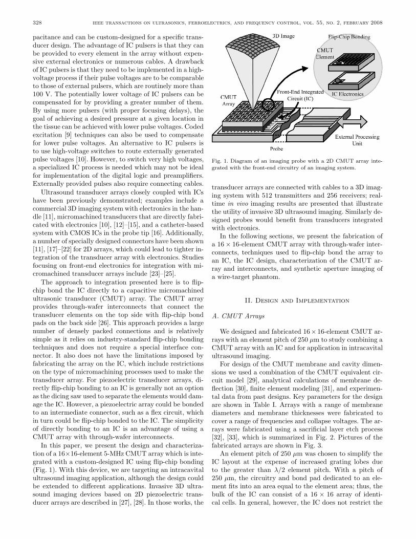
In this paper, we present the design and characteriza-tion of a 16×16-element 5-MHz CMUT array which is inte-grated with a custom-designed IC using flip-chip bonding(Fig. 1). With this device, we are targeting an intracavitalultrasound imaging application, although the design couldbe extended to different applications. Invasive 3D ultra-sound imaging devices based on 2D piezoelectric trans-ducer arrays are described in [27], [28]. In those works, the
Fig. 1. Diagram of an imaging probe with a 2D CMUT array inte-grated with the front-end circuitry of an imaging system.
transducer arrays are connected with cables to a 3D imag-ing system with 512 transmitters and 256 receivers; real-time in vivo imaging results are presented that illustratethe utility of invasive 3D ultrasound imaging. Similarly de-signed probes would benefit from transducers integratedwith electronics.
In the following sections, we present the fabrication ofa 16 × 16-element CMUT array with through-wafer inter-connects, techniques used to flip-chip bond the array toan IC, the IC design, characterization of the CMUT ar-ray and interconnects, and synthetic aperture imaging ofa wire-target phantom.
II. Design and Implementation
A. CMUT Arrays
We designed and fabricated 16× 16-element CMUT ar-rays with an element pitch of 250 µm to study combining aCMUT array with an IC and for application in intracavitalultrasound imaging.
For design of the CMUT membrane and cavity dimen-sions we used a combination of the CMUT equivalent cir-cuit model [29], analytical calculations of membrane de-flection [30], finite element modeling [31], and experimen-tal data from past designs. Key parameters for the designare shown in Table I. Arrays with a range of membranediameters and membrane thicknesses were fabricated tocover a range of frequencies and collapse voltages. The ar-rays were fabricated using a sacrificial layer etch process[32], [33], which is summarized in Fig. 2. Pictures of thefabricated arrays are shown in Fig. 3.
An element pitch of 250 µm was chosen to simplify theIC layout at the expense of increased grating lobes dueto the greater than λ/2 element pitch. With a pitch of250 µm, the circuitry and bond pad dedicated to an ele-ment fits into an area equal to the element area; thus, thebulk of the IC can consist of a 16 × 16 array of identi-cal cells. In general, however, the IC does not restrict the
wygant et al.: integration of 2d cmut arrays with front-end electronics 329
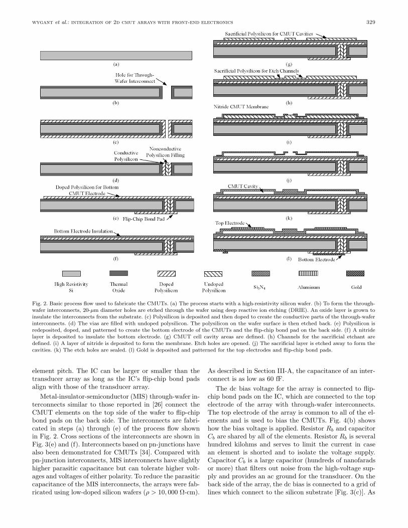
Fig. 2. Basic process flow used to fabricate the CMUTs. (a) The process starts with a high-resistivity silicon wafer. (b) To form the through-wafer interconnects, 20-µm diameter holes are etched through the wafer using deep reactive ion etching (DRIE). An oxide layer is grown toinsulate the interconnects from the substrate. (c) Polysilicon is deposited and then doped to create the conductive parts of the through-waferinterconnects. (d) The vias are filled with undoped polysilicon. The polysilicon on the wafer surface is then etched back. (e) Polysilicon isredeposited, doped, and patterned to create the bottom electrode of the CMUTs and the flip-chip bond pad on the back side. (f) A nitridelayer is deposited to insulate the bottom electrode. (g) CMUT cell cavity areas are defined. (h) Channels for the sacrificial etchant aredefined. (i) A layer of nitride is deposited to form the membrane. Etch holes are opened. (j) The sacrificial layer is etched away to form thecavities. (k) The etch holes are sealed. (l) Gold is deposited and patterned for the top electrodes and flip-chip bond pads.
element pitch. The IC can be larger or smaller than thetransducer array as long as the IC’s flip-chip bond padsalign with those of the transducer array.
Metal-insulator-semiconductor (MIS) through-wafer in-terconnects similar to those reported in [26] connect theCMUT elements on the top side of the wafer to flip-chipbond pads on the back side. The interconnects are fabri-cated in steps (a) through (e) of the process flow shownin Fig. 2. Cross sections of the interconnects are shown inFig. 3(e) and (f). Interconnects based on pn-junctions havealso been demonstrated for CMUTs [34]. Compared withpn-junction interconnects, MIS interconnects have slightlyhigher parasitic capacitance but can tolerate higher volt-ages and voltages of either polarity. To reduce the parasiticcapacitance of the MIS interconnects, the arrays were fab-ricated using low-doped silicon wafers (ρ > 10, 000 Ω-cm).
As described in Section III-A, the capacitance of an inter-connect is as low as 60 fF.
The dc bias voltage for the array is connected to flip-chip bond pads on the IC, which are connected to the topelectrode of the array with through-wafer interconnects.The top electrode of the array is common to all of the el-ements and is used to bias the CMUTs. Fig. 4(b) showshow the bias voltage is applied. Resistor Rb and capacitorCb are shared by all of the elements. Resistor Rb is severalhundred kilohms and serves to limit the current in casean element is shorted and to isolate the voltage supply.Capacitor Cb is a large capacitor (hundreds of nanofaradsor more) that filters out noise from the high-voltage sup-ply and provides an ac ground for the transducer. On theback side of the array, the dc bias is connected to a grid oflines which connect to the silicon substrate [Fig. 3(c)]. As
330 ieee transactions on ultrasonics, ferroelectrics, and frequency control, vol. 55, no. 2, february 2008
Fig. 3. Pictures and scanning electron micrographs (SEMs) of the CMUT array and through-wafer interconnects. (a) SEM of an individual250-µm × 250-µm element. (b) Closeup of several 30-µm-diameter membranes. (c) Back side of the CMUT array. (d) Back side of severalelements. (e) Cross section of a device flip-chip bonded using anisotropic conducting film (ACF). (f) SEM of the edge of a cleaved wafershowing a through-wafer via.
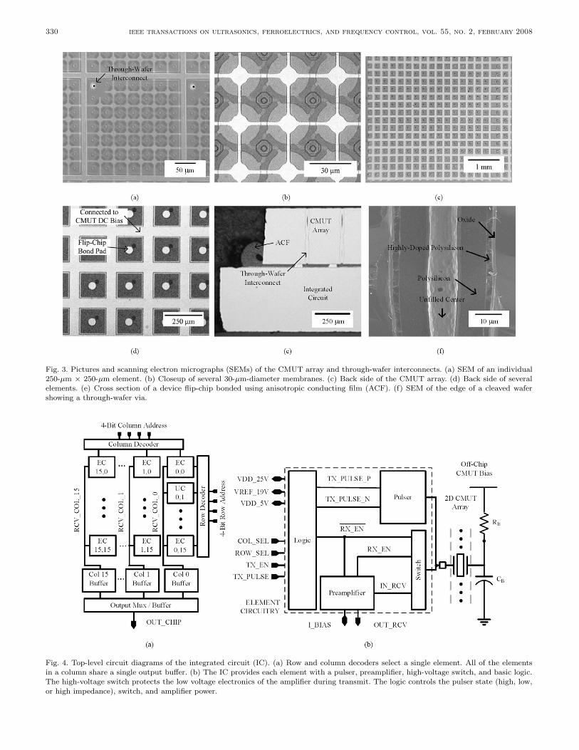
Fig. 4. Top-level circuit diagrams of the integrated circuit (IC). (a) Row and column decoders select a single element. All of the elementsin a column share a single output buffer. (b) The IC provides each element with a pulser, preamplifier, high-voltage switch, and basic logic.The high-voltage switch protects the low voltage electronics of the amplifier during transmit. The logic controls the pulser state (high, low,or high impedance), switch, and amplifier power.
wygant et al.: integration of 2d cmut arrays with front-end electronics 331
TABLE ICMUT Array Parameters.
Array size (elements) 16 × 16Element pitch (µm) 250CMUT membrane diameter (µm) 24, 30, 36Number of membranes per element 24, 35, 48Membrane thickness (µm) 0.6, 0.5, 0.8Cavity thickness (µm) 0.1Insulating layer thickness (µm) 0.15Silicon substrate thickness (µm) 400Flip-chip bond pad diameter (µm) 50Through-wafer interconnect diameter (µm) 20Silicon wafer resistivity (Ω-cm) > 10,000
described in Section III-A, the silicon substrate is biasedto reduce the parasitic capacitances of the through-waferinterconnect, the flip-chip bond pad, and the bottom elec-trode of the CMUT.
A drawback of applying dc bias voltage to the top elec-trode of the array is that it is applied to the side of thearray which is exposed to the patient. Alternatively, thetop electrode could be grounded and the voltage suppliesfor the IC shifted by the desired dc bias voltage.
B. Integrated Circuit with Pulsers and Preamplifiers
The IC provides a transmit and receive circuit to everyelement of the array. This circuit consists of a pulser, atransimpedance amplifier, and a switch that protects thelow-voltage amplifier electronics from the pulser’s output.A circuit with the same basic topology was first imple-mented in a 2.5-V standard CMOS process [35]. For thiswork, we adapted those low-voltage circuits to a high-voltage process and made an array of circuits for imagingwith a 2D array.
The circuitry dedicated to each transducer element isdesigned to occupy the same area as the element (250-µm× 250-µm). Each column of elements shares an outputbuffer which drives the load associated with the imag-ing system and connecting cables. The IC was designedfor a high-voltage process (National Semiconductor, SantaClara, CA). This process has two metal layers and a min-imum feature size of 1.5 µm. Devices provided by the pro-cess include standard and high-voltage 1.5-µm CMOS de-vices, bipolar devices, and DMOS devices. For the pulsercircuitry we use the high-voltage CMOS devices. For theremaining circuitry we use the standard CMOS devices.
To simplify the circuit design and data acquisition forthis initial implementation of the electronics, the IC usesa single element at a time for transmit and receive. Theactive element is selected with four-bit row and columnaddresses. Although this design is simple compared to amultichannel system, the IC can be used for pulse-echocharacterization of each element in the array and for real-time 3D synthetic-aperture imaging. The top-level designof the IC is illustrated in Fig. 4. Schematics of the pulser,preamplifier, and switch are shown in Fig. 5.
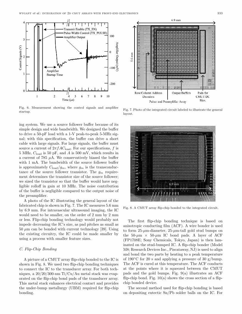
The timing of the transmit pulse and preamplifierstartup is shown in Fig. 6. When the signal TX EN
[Fig. 5(d)] is high, the selected element is used to trans-mit: the preamplifier is turned off, the protection switchis opened, and the pulser output voltage is controlled byTX PULSE. The duration of the TX PULSE signal de-termines the duration of the output pulse. When TX ENis low, then the selected element is used for receive: thepreamplifier is turned on, the protection switch is closed,and the pulser output has a high impedance.
The receive circuitry uses a 5-V power supply and con-sumes 9 mW of power when an amplifier is enabled forreceive. About 60% of the power is used by the enabledoutput buffer; the remainder is used by the enabled pream-plifier. The power consumption was determined such thata 16-channel implementation of the IC would consume lessthan 150 mW, which is comparable to the 100-mW powerlimit given in [16] for an intravascular ultrasound IC.
To target low power or high channel count applications,the IC could be designed to consume less power per chan-nel. Using the same IC process technology, the power con-sumption of the preamplifier could be reduced primarily atthe expense of noise performance. Using a process with alower supply voltage and finer features would reduce powerconsumption for both the preamplifier and buffer. Somebuffer power could be saved by using a more efficient buffercircuit. More significantly, buffer power could be saved byreducing the total gain of the preamplifier and buffer. Ide-ally the gain of the preamplifier and buffer should be justlarge enough that the noise at the output of the bufferdominates the input-referred noise of the following stage.If the gain is any higher, the SNR for the system doesnot improve but the buffer consumes more power to swinglarger voltages. In the IC presented, assuming the bufferdrives the input of a typical ultrasound data acquisitionsystem, the total preamplifier and buffer gain could be re-duced without loss in SNR.
The pulser circuit [Fig. 5(a)] is based on the first stageof the pulser circuit described in [36]. High-voltage tran-sistors MN1, MN1′, MP1, and MP1′ are used to increasethe pulse voltage. The pulser’s output is 25 V, 0 V, orhigh impedance, depending on the values of input signalsIN P and IN N. The high impedance state is used dur-ing receive. The transistors of the pulser circuit are sizedto provide pulses as short as 100 ns to a 2.5-pF load. Thepulser occupies roughly one-third of the 250-µm × 250-µmIC area dedicated to each element.
The preamplifier circuit [Fig. 5(b)] is a transimpedanceamplifier [37], [38] composed of a single-ended amplifierand a 430-kΩ feedback resistor. The single-ended ampli-fier consists of a common-source amplifier with a gain of−100 V/V followed by a source follower. A transimpedanceamplifier acts as a current-to-voltage converter. It hasa low input impedance which is well-suited for high-impedance sources [37]. The preamplifier was designed tohave minimal noise, a bandwidth of 10 MHz, and a powerconsumption of 4 mW. For circuit simulations, the inputto the amplifier was modeled with the CMUT equivalentcircuit described in [29] with an additional parasitic ca-pacitance of 1 pF.
332 ieee transactions on ultrasonics, ferroelectrics, and frequency control, vol. 55, no. 2, february 2008
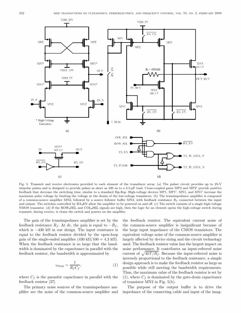
Fig. 5. Transmit and receive electronics provided to each element of the transducer array. (a) The pulser circuit provides up to 25-Vunipolar pulses and is designed to provide pulses as short as 100 ns to a 2.5-pF load. Cross-coupled gates MP2 and MP2′ provide positivefeedback that decrease the switching time, similar to a standard flip-flop. High-voltage devices MP1, MP1′, MN1, and MN1′ increase themaximum pulse voltage by limiting the voltage at the drains of the low-voltage transistors. (b) The transimpedance amplifier is composedof a common-source amplifier MN2, followed by a source follower buffer MN3, with feedback resistance Rf connected between the inputand output. The switches controlled by RX EN allow the amplifier to be powered on and off. (c) The switch consists of a single high-voltageNMOS transistor. (d) If the ROW SEL and COL SEL signals are high, then the logic for an element opens the high-voltage switch duringtransmit; during receive, it closes the switch and powers on the amplifier.
The gain of the transimpedance amplifier is set by thefeedback resistance Rf . At dc, the gain is equal to −Rf ,which is −430 kΩ in our design. The input resistance isequal to the feedback resistor divided by the open-loopgain of the single-ended amplifier (430 kΩ/100 = 4.3 kΩ).When the feedback resistance is so large that the band-width is dominated by the capacitance in parallel with thefeedback resistor, the bandwidth is approximated by
ωamp =1
RfCf, (1)
where Cf is the parasitic capacitance in parallel with thefeedback resistor [37].
The primary noise sources of the transimpedance am-plifier are the noise of the common-source amplifier and
the feedback resistor. The equivalent current noise ofthe common-source amplifier is insignificant because ofthe large input impedance of the CMOS transistors. Theequivalent voltage noise of the common-source amplifier islargely affected by device sizing and the circuit technologyused. The feedback resistor value has the largest impact onnoise performance. It contributes an input-referred noisecurrent of
√4kT/Rf . Because the input-referred noise is
inversely proportional to the feedback resistance, a simpledesign approach is to make the feedback resistor as large aspossible while still meeting the bandwidth requirements.Thus, the maximum value of the feedback resistor is set by(1), where Cf is dominated by the gate-drain capacitanceof transistor MN2 in Fig. 5(b).
The purpose of the output buffer is to drive theimpedance of the connecting cable and input of the imag-
wygant et al.: integration of 2d cmut arrays with front-end electronics 333
Fig. 6. Measurement showing the control signals and amplifierstartup.
ing system. We use a source follower buffer because of itssimple design and wide bandwidth. We designed the bufferto drive a 50-pF load with a 1-V peak-to-peak 5-MHz sig-nal; with this specification, the buffer can drive a shortcable with large signals. For large signals, the buffer mustsource a current of 2πfACload. For our specifications, f is5 MHz, Cload is 50 pF, and A is 500 mV, which results ina current of 785 µA. We conservatively biased the bufferwith 1 mA. The bandwidth of the source follower bufferis approximately Cload/gm, where gm is the transconduc-tance of the source follower transistor. The gm require-ment determines the transistor size of the source follower;we sized the transistor so that the buffer would have neg-ligible rolloff in gain at 10 MHz. The noise contributionof the buffer is negligible compared to the output noise ofthe preamplifier.
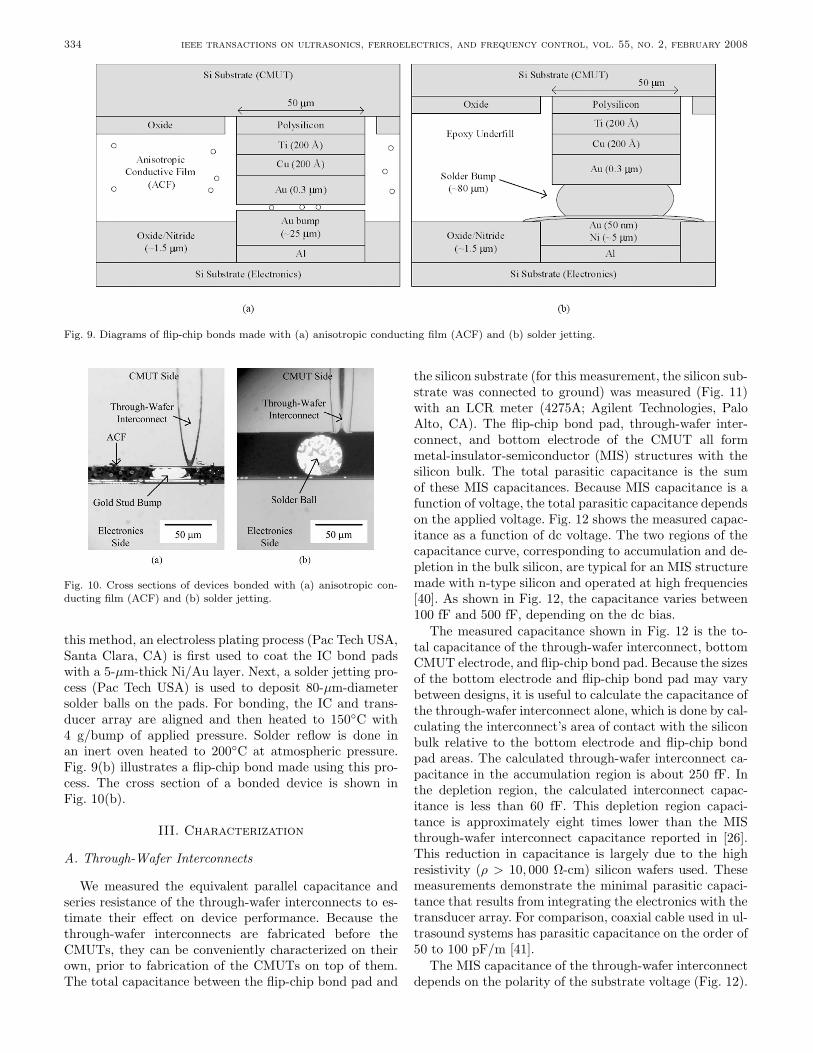
A photo of the IC illustrating the general layout of thefabricated chip is shown in Fig. 7. The IC measures 5.6 mmby 6.9 mm. For intravascular ultrasound imaging, the ICwould need to be smaller, on the order of 2 mm by 2 mmor less. Flip-chip bonding technology would probably notimpede decreasing the IC’s size, as pad pitches as small as50 µm can be bonded with current technology [39]. Usingthe existing circuitry, the IC could be made smaller byusing a process with smaller feature sizes.
C. Flip-Chip Bonding
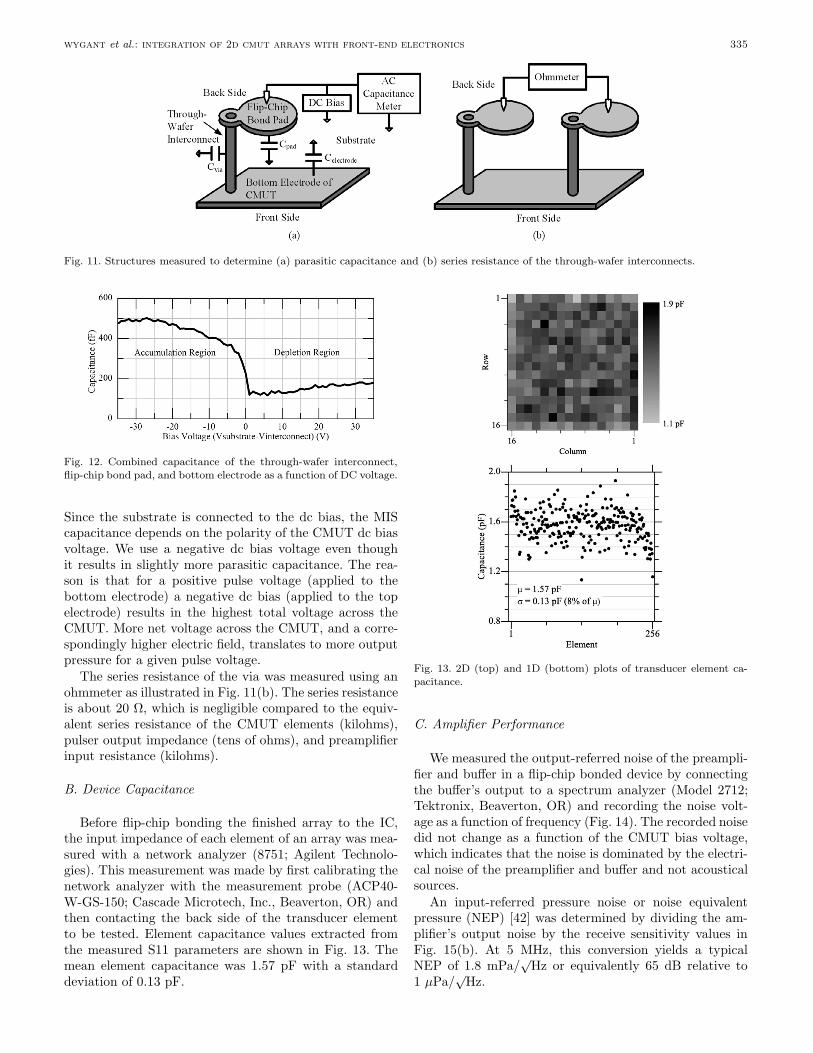
A picture of a CMUT array flip-chip bonded to the IC isshown in Fig. 8. We used two flip-chip bonding techniquesto connect the IC to the transducer array. For both tech-niques, a 20/20/300-nm Ti/Cu/Au metal stack was evap-orated on the flip-chip bond pads of the transducer array.This metal stack enhances electrical contact and providesthe under-bump metallurgy (UBM) required for flip-chipbonding.
Fig. 7. Photo of the integrated circuit labeled to illustrate the generallayout.
Fig. 8. A CMUT array flip-chip bonded to the integrated circuit.
The first flip-chip bonding technique is based onanisotropic conducting film (ACF). A wire bonder is usedto form 25-µm-diameter, 25-µm-tall gold stud bumps onthe 50-µm × 50-µm IC bond pads. A layer of ACF(FP1708E; Sony Chemicals, Tokyo, Japan) is then lam-inated on the stud-bumped IC. A flip-chip bonder (ModelM8; Research Devices Inc., Piscataway, NJ) is used to alignand bond the two parts by heating to a peak temperatureof 190C for 20 s and applying a pressure of 30 g/bump.The ACF is cured at this temperature. The ACF conductsat the points where it is squeezed between the CMUTpads and the gold bumps. Fig. 9(a) illustrates an ACFflip-chip bond. Fig. 10(a) shows the cross section of a flip-chip bonded device.
The second method used for flip-chip bonding is basedon depositing eutectic Sn/Pb solder balls on the IC. For
334 ieee transactions on ultrasonics, ferroelectrics, and frequency control, vol. 55, no. 2, february 2008
Fig. 9. Diagrams of flip-chip bonds made with (a) anisotropic conducting film (ACF) and (b) solder jetting.
Fig. 10. Cross sections of devices bonded with (a) anisotropic con-ducting film (ACF) and (b) solder jetting.
this method, an electroless plating process (Pac Tech USA,Santa Clara, CA) is first used to coat the IC bond padswith a 5-µm-thick Ni/Au layer. Next, a solder jetting pro-cess (Pac Tech USA) is used to deposit 80-µm-diametersolder balls on the pads. For bonding, the IC and trans-ducer array are aligned and then heated to 150C with4 g/bump of applied pressure. Solder reflow is done inan inert oven heated to 200C at atmospheric pressure.Fig. 9(b) illustrates a flip-chip bond made using this pro-cess. The cross section of a bonded device is shown inFig. 10(b).
III. Characterization
A. Through-Wafer Interconnects
We measured the equivalent parallel capacitance andseries resistance of the through-wafer interconnects to es-timate their effect on device performance. Because thethrough-wafer interconnects are fabricated before theCMUTs, they can be conveniently characterized on theirown, prior to fabrication of the CMUTs on top of them.The total capacitance between the flip-chip bond pad and
the silicon substrate (for this measurement, the silicon sub-strate was connected to ground) was measured (Fig. 11)with an LCR meter (4275A; Agilent Technologies, PaloAlto, CA). The flip-chip bond pad, through-wafer inter-connect, and bottom electrode of the CMUT all formmetal-insulator-semiconductor (MIS) structures with thesilicon bulk. The total parasitic capacitance is the sumof these MIS capacitances. Because MIS capacitance is afunction of voltage, the total parasitic capacitance dependson the applied voltage. Fig. 12 shows the measured capac-itance as a function of dc voltage. The two regions of thecapacitance curve, corresponding to accumulation and de-pletion in the bulk silicon, are typical for an MIS structuremade with n-type silicon and operated at high frequencies[40]. As shown in Fig. 12, the capacitance varies between100 fF and 500 fF, depending on the dc bias.
The measured capacitance shown in Fig. 12 is the to-tal capacitance of the through-wafer interconnect, bottomCMUT electrode, and flip-chip bond pad. Because the sizesof the bottom electrode and flip-chip bond pad may varybetween designs, it is useful to calculate the capacitance ofthe through-wafer interconnect alone, which is done by cal-culating the interconnect’s area of contact with the siliconbulk relative to the bottom electrode and flip-chip bondpad areas. The calculated through-wafer interconnect ca-pacitance in the accumulation region is about 250 fF. Inthe depletion region, the calculated interconnect capac-itance is less than 60 fF. This depletion region capaci-tance is approximately eight times lower than the MISthrough-wafer interconnect capacitance reported in [26].This reduction in capacitance is largely due to the highresistivity (ρ > 10, 000 Ω-cm) silicon wafers used. Thesemeasurements demonstrate the minimal parasitic capaci-tance that results from integrating the electronics with thetransducer array. For comparison, coaxial cable used in ul-trasound systems has parasitic capacitance on the order of50 to 100 pF/m [41].
The MIS capacitance of the through-wafer interconnectdepends on the polarity of the substrate voltage (Fig. 12).
wygant et al.: integration of 2d cmut arrays with front-end electronics 335
Fig. 11. Structures measured to determine (a) parasitic capacitance and (b) series resistance of the through-wafer interconnects.
Fig. 12. Combined capacitance of the through-wafer interconnect,flip-chip bond pad, and bottom electrode as a function of DC voltage.
Since the substrate is connected to the dc bias, the MIScapacitance depends on the polarity of the CMUT dc biasvoltage. We use a negative dc bias voltage even thoughit results in slightly more parasitic capacitance. The rea-son is that for a positive pulse voltage (applied to thebottom electrode) a negative dc bias (applied to the topelectrode) results in the highest total voltage across theCMUT. More net voltage across the CMUT, and a corre-spondingly higher electric field, translates to more outputpressure for a given pulse voltage.
The series resistance of the via was measured using anohmmeter as illustrated in Fig. 11(b). The series resistanceis about 20 Ω, which is negligible compared to the equiv-alent series resistance of the CMUT elements (kilohms),pulser output impedance (tens of ohms), and preamplifierinput resistance (kilohms).
B. Device Capacitance
Before flip-chip bonding the finished array to the IC,the input impedance of each element of an array was mea-sured with a network analyzer (8751; Agilent Technolo-gies). This measurement was made by first calibrating thenetwork analyzer with the measurement probe (ACP40-W-GS-150; Cascade Microtech, Inc., Beaverton, OR) andthen contacting the back side of the transducer elementto be tested. Element capacitance values extracted fromthe measured S11 parameters are shown in Fig. 13. Themean element capacitance was 1.57 pF with a standarddeviation of 0.13 pF.
Fig. 13. 2D (top) and 1D (bottom) plots of transducer element ca-pacitance.
C. Amplifier Performance
We measured the output-referred noise of the preampli-fier and buffer in a flip-chip bonded device by connectingthe buffer’s output to a spectrum analyzer (Model 2712;Tektronix, Beaverton, OR) and recording the noise volt-age as a function of frequency (Fig. 14). The recorded noisedid not change as a function of the CMUT bias voltage,which indicates that the noise is dominated by the electri-cal noise of the preamplifier and buffer and not acousticalsources.
An input-referred pressure noise or noise equivalentpressure (NEP) [42] was determined by dividing the am-plifier’s output noise by the receive sensitivity values inFig. 15(b). At 5 MHz, this conversion yields a typicalNEP of 1.8 mPa/
√Hz or equivalently 65 dB relative to
1 µPa/√
Hz.
336 ieee transactions on ultrasonics, ferroelectrics, and frequency control, vol. 55, no. 2, february 2008
TABLE IIUltrasound Properties of Materials Used for Testing Imaging Arrays.
Soybean oil [52] Water [53] Tissue [54]
Density (kg/m3) 913 1000 1050Sound velocity (m/s) 1480 1497 1570Acoustic impedance (MRayls) 1.35 1.49 1.65α (1/m-Hzk) 7.3 × 10⁻¹² 2.2 × 10⁻¹⁴ 5.8 × 10⁻⁶
k 1.85 2 1
Fig. 14. Output noise of the preamplifier measured with a spectrumanalyzer.
Comparing the frequency content of the one-way hy-drophone measurements and the pulse-echo measurementsindicates that the amplifier bandwidth does not limit thetransducer’s bandwidth. This is in agreement with the sim-ulated bandwidth of 9.5 MHz for a 2-pF source capaci-tance. Measuring the amplifier’s frequency response on itsown is difficult because capacitance of more than a few pi-cofarads at the input significantly reduces the amplifier’sbandwidth. An on-chip test structure as used in [16] is oneway of characterizing the amplifier without connecting itto a transducer.
D. Pulse-Echo Signal from a Plane Reflector
For pulse-echo and imaging tests, a 5-cm × 5-cm × 4-cm acrylic tank was built. A rectangular hole was cut inthe bottom of the tank to create an acoustic window forthe array. The tank was then glued to a ceramic packagethat contained the flip-chip bonded device. For imagingand pulse-echo tests, the tank was filled with soybean oil.
We use soybean oil instead of water because it is non-conducting; thus, we can test the device in immersion with-out insulating the bond wires and electrodes of the CMUTand IC. Furthermore, the acoustic impedance and speedin soybean oil are similar to those for water and tissue(Table II). For in vivo testing, the device would need to beinsulated. We have previously demonstrated CMUTs insu-lated with parylene for operation in water [43]. In general,insulating procedures used for piezoelectric arrays can alsobe used for CMUT arrays.
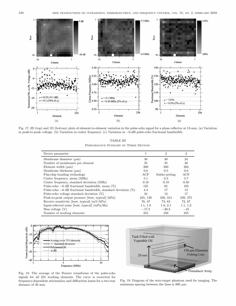
To measure the pulse-echo signal received from a planereflector, we acquired the pulse-echo signal from the oil-air interface at 15 mm for each element of the array(Figs. 16, 17, and 18) with an oscilloscope (model 54825;
Fig. 15. Output pressure and receive sensitivity measurements basedon hydrophone and pulse-echo measurements. (a) Transducer out-put pressure normalized to the face of the transducer. (b) Receivesensitivity at the output of the amplifier as a function of DC biasvoltage.
Agilent Technologies). The frequency responses show widebandwidth and good element-to-element uniformity. In thepulse-echo signals shown in Fig. 16(a) and (b), there aresmall signals following the main pulse. These signals mightbe due to crosstalk between the elements [2], particularlysince they are more pronounced for elements in the center.A way of reducing this crosstalk could be to coat the arraywith a thin attenuating layer that would suppress laterallymoving waves [44]; the insulating or matching layers usedto coat the array could also serve this purpose. The charac-terization and suppression of crosstalk in CMUTs [45]–[48]is an ongoing topic of investigation.
The peak-to-peak transmitted pressure was measuredfor four elements of the array. These four elements includedthe one with the largest pulse-echo response and three withtypical pulse-echo responses. The pressure was measuredat a distance of 4 mm from the array using a calibrated hy-drophone (model PZT-Z44-0400; Onda Corporation, Sun-nyvale, CA). The pressure was then normalized to the face
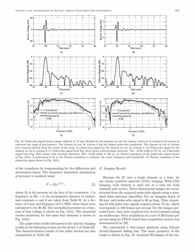
wygant et al.: integration of 2d cmut arrays with front-end electronics 337
Fig. 16. Pulse-echo signals from a plane reflector at 15 mm. Results for the elements at row 16, column 4 and row 8, column 8 are chosen torepresent the range of performance. The element at row 16, column 4 has the largest pulse-echo amplitude. The element at row 8, column8 is a typical element from the center of the array. (a) Pulse-echo signal for the element at row 16, column 4. (b) Pulse-echo signal for theelement at row 8, column 8. (c) Pulse-echo signal from Fig. 16(a) shown with envelope detection. The −6-dB width is 177 ns. (d) Pulse-echosignal from Fig. 16(b) shown with envelope detection. The −6-dB width is 190 ns. (e) Fourier transform of the pulse-echo signal shownin Fig. 16(a). A polynomial is fit to the Fourier transform to estimate the center frequency and bandwidth. (f) Fourier transform of thepulse-echo signal shown in Fig. 16(b).
of the transducer by compensating for the diffraction andattenuation losses. The frequency dependent attenuationof pressure is modeled using
P = P0eαfkz, (2)
where P0 is the pressure at the face of the transducer, f isfrequency in Hz, z is the propagation distance in meters,and constants α and k are taken from Table II. At a dis-tance of 4 mm and frequency of 5.1 MHz, these losses werecalculated to be 26 dB. The normalized pressure as a func-tion of bias voltage is shown in Fig. 15(a). The measuredreceive sensitivity for the same four elements is shown inFig. 15(b).
The pulse-echo results discussed so far and the imagingresults in the following section are for device 1 of Table III.The characterization results of two other devices are alsosummarized in Table III.
E. Imaging Results
Because the IC uses a single element at a time, weuse classic synthetic aperture (CSA) imaging. With CSAimaging, each element is used one at a time for bothtransmit and receive. Three-dimensional images are recon-structed from the acquired pulse-echo signals using a stan-dard delay-and-sum algorithm. For an imaging depth of30 mm, each pulse-echo signal is 40 µs long. Thus, acquir-ing all 256 pulse-echo signals requires about 10 ms, whichcorresponds to 100 frames per second. For the images pre-sented here, data were acquired over several minutes usingan oscilloscope. Data acquisition at a rate of 30 frames persecond using an FPGA-based data acquisition system wasdemonstrated in [49].
We constructed a wire-target phantom using 150-µm(6-mil)-diameter fishing line. The basic geometry of thetarget is shown in Fig. 19. Acquired 2D images of the tar-
338 ieee transactions on ultrasonics, ferroelectrics, and frequency control, vol. 55, no. 2, february 2008
Fig. 17. 2D (top) and 1D (bottom) plots of element-to-element variation in the pulse-echo signal for a plane reflector at 15-mm. (a) Variationin peak-to-peak voltage. (b) Variation in center frequency. (c) Variation in −6-dB pulse-echo fractional bandwidth.
TABLE IIIPerformance Summary of Three Devices.
Device parameter 1 2 3
Membrane diameter (µm) 30 30 24Number of membranes per element 35 35 48Element width (µm) 200 200 204Membrane thickness (µm) 0.6 0.5 0.6Flip-chip bonding technology ACF Solder-jetting ACFCenter frequency, mean (MHz) 5.1 2.3 5.7Center frequency, standard deviation (MHz) 0.10 0.19 0.50Pulse-echo −6 dB fractional bandwidth, mean (%) 125 65 105Pulse-echo −6 dB fractional bandwidth, standard deviation (%) 4.3 17 13Pulse-echo voltage standard deviation (%) 34 12 17Peak-to-peak output pressure [best, typical] (kPa) 225, 139 330, 314 339, 275Receive sensitivity [best, typical] (mV/kPa) 76, 47 73, 63 72, 67Input-referred noise [best, typical] (mPa/Hz) 1.1, 1.8 1.8, 2.1 1.1, 1.2Bias voltage (V) −17.3 −30.3 −45Number of working elements 255 256 255
Fig. 18. The average of the Fourier transforms of the pulse-echosignals for all 255 working elements. The curve is corrected forfrequency-dependent attenuation and diffraction losses for a two-waydistance of 30 mm.
Fig. 19. Diagram of the wire-target phantom used for imaging. Theminimum spacing between the lines is 800 µm.
wygant et al.: integration of 2d cmut arrays with front-end electronics 339
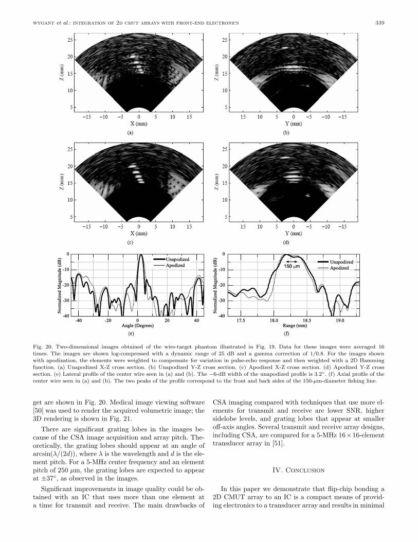
Fig. 20. Two-dimensional images obtained of the wire-target phantom illustrated in Fig. 19. Data for these images were averaged 16times. The images are shown log-compressed with a dynamic range of 25 dB and a gamma correction of 1/0.8. For the images shownwith apodization, the elements were weighted to compensate for variation in pulse-echo response and then weighted with a 2D Hammingfunction. (a) Unapodized X-Z cross section. (b) Unapodized Y-Z cross section. (c) Apodized X-Z cross section. (d) Apodized Y-Z crosssection. (e) Lateral profile of the center wire seen in (a) and (b). The −6-dB width of the unapodized profile is 3.2. (f) Axial profile of thecenter wire seen in (a) and (b). The two peaks of the profile correspond to the front and back sides of the 150-µm-diameter fishing line.
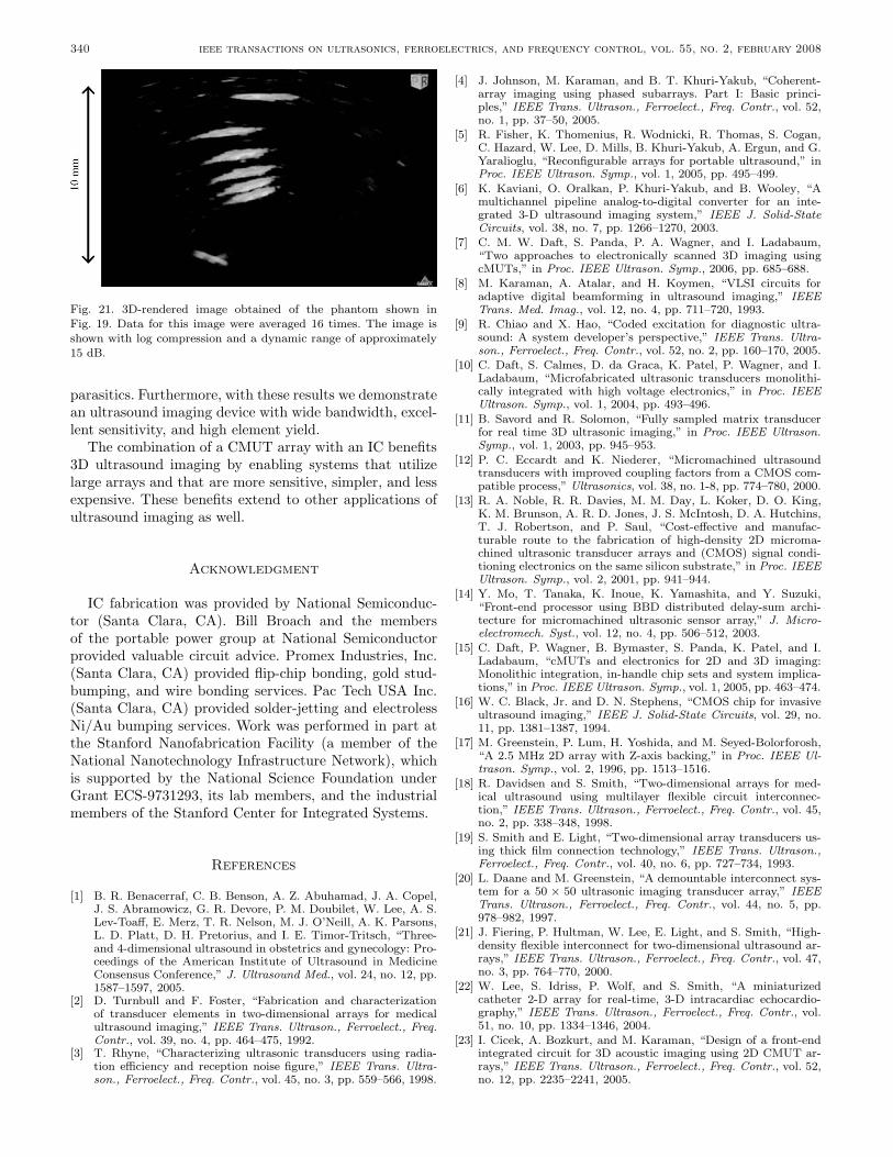
get are shown in Fig. 20. Medical image viewing software[50] was used to render the acquired volumetric image; the3D rendering is shown in Fig. 21.
There are significant grating lobes in the images be-cause of the CSA image acquisition and array pitch. The-oretically, the grating lobes should appear at an angle ofarcsin(λ/(2d)), where λ is the wavelength and d is the ele-ment pitch. For a 5-MHz center frequency and an elementpitch of 250 µm, the grating lobes are expected to appearat ±37, as observed in the images.
Significant improvements in image quality could be ob-tained with an IC that uses more than one element ata time for transmit and receive. The main drawbacks of
CSA imaging compared with techniques that use more el-ements for transmit and receive are lower SNR, highersidelobe levels, and grating lobes that appear at smalleroff-axis angles. Several transmit and receive array designs,including CSA, are compared for a 5-MHz 16×16-elementtransducer array in [51].
IV. Conclusion
In this paper we demonstrate that flip-chip bonding a2D CMUT array to an IC is a compact means of provid-ing electronics to a transducer array and results in minimal
340 ieee transactions on ultrasonics, ferroelectrics, and frequency control, vol. 55, no. 2, february 2008
Fig. 21. 3D-rendered image obtained of the phantom shown inFig. 19. Data for this image were averaged 16 times. The image isshown with log compression and a dynamic range of approximately15 dB.
parasitics. Furthermore, with these results we demonstratean ultrasound imaging device with wide bandwidth, excel-lent sensitivity, and high element yield.
The combination of a CMUT array with an IC benefits3D ultrasound imaging by enabling systems that utilizelarge arrays and that are more sensitive, simpler, and lessexpensive. These benefits extend to other applications ofultrasound imaging as well.
Acknowledgment
IC fabrication was provided by National Semiconduc-tor (Santa Clara, CA). Bill Broach and the membersof the portable power group at National Semiconductorprovided valuable circuit advice. Promex Industries, Inc.(Santa Clara, CA) provided flip-chip bonding, gold stud-bumping, and wire bonding services. Pac Tech USA Inc.(Santa Clara, CA) provided solder-jetting and electrolessNi/Au bumping services. Work was performed in part atthe Stanford Nanofabrication Facility (a member of theNational Nanotechnology Infrastructure Network), whichis supported by the National Science Foundation underGrant ECS-9731293, its lab members, and the industrialmembers of the Stanford Center for Integrated Systems.
References
[1] B. R. Benacerraf, C. B. Benson, A. Z. Abuhamad, J. A. Copel,J. S. Abramowicz, G. R. Devore, P. M. Doubilet, W. Lee, A. S.Lev-Toaff, E. Merz, T. R. Nelson, M. J. O’Neill, A. K. Parsons,L. D. Platt, D. H. Pretorius, and I. E. Timor-Tritsch, “Three-and 4-dimensional ultrasound in obstetrics and gynecology: Pro-ceedings of the American Institute of Ultrasound in MedicineConsensus Conference,” J. Ultrasound Med., vol. 24, no. 12, pp.1587–1597, 2005.
[2] D. Turnbull and F. Foster, “Fabrication and characterizationof transducer elements in two-dimensional arrays for medicalultrasound imaging,” IEEE Trans. Ultrason., Ferroelect., Freq.Contr., vol. 39, no. 4, pp. 464–475, 1992.
[3] T. Rhyne, “Characterizing ultrasonic transducers using radia-tion efficiency and reception noise figure,” IEEE Trans. Ultra-son., Ferroelect., Freq. Contr., vol. 45, no. 3, pp. 559–566, 1998.
[4] J. Johnson, M. Karaman, and B. T. Khuri-Yakub, “Coherent-array imaging using phased subarrays. Part I: Basic princi-ples,” IEEE Trans. Ultrason., Ferroelect., Freq. Contr., vol. 52,no. 1, pp. 37–50, 2005.
[5] R. Fisher, K. Thomenius, R. Wodnicki, R. Thomas, S. Cogan,C. Hazard, W. Lee, D. Mills, B. Khuri-Yakub, A. Ergun, and G.Yaralioglu, “Reconfigurable arrays for portable ultrasound,” inProc. IEEE Ultrason. Symp., vol. 1, 2005, pp. 495–499.
[6] K. Kaviani, O. Oralkan, P. Khuri-Yakub, and B. Wooley, “Amultichannel pipeline analog-to-digital converter for an inte-grated 3-D ultrasound imaging system,” IEEE J. Solid-StateCircuits, vol. 38, no. 7, pp. 1266–1270, 2003.
[7] C. M. W. Daft, S. Panda, P. A. Wagner, and I. Ladabaum,“Two approaches to electronically scanned 3D imaging usingcMUTs,” in Proc. IEEE Ultrason. Symp., 2006, pp. 685–688.
[8] M. Karaman, A. Atalar, and H. Koymen, “VLSI circuits foradaptive digital beamforming in ultrasound imaging,” IEEETrans. Med. Imag., vol. 12, no. 4, pp. 711–720, 1993.
[9] R. Chiao and X. Hao, “Coded excitation for diagnostic ultra-sound: A system developer’s perspective,” IEEE Trans. Ultra-son., Ferroelect., Freq. Contr., vol. 52, no. 2, pp. 160–170, 2005.
[10] C. Daft, S. Calmes, D. da Graca, K. Patel, P. Wagner, and I.Ladabaum, “Microfabricated ultrasonic transducers monolithi-cally integrated with high voltage electronics,” in Proc. IEEEUltrason. Symp., vol. 1, 2004, pp. 493–496.
[11] B. Savord and R. Solomon, “Fully sampled matrix transducerfor real time 3D ultrasonic imaging,” in Proc. IEEE Ultrason.Symp., vol. 1, 2003, pp. 945–953.
[12] P. C. Eccardt and K. Niederer, “Micromachined ultrasoundtransducers with improved coupling factors from a CMOS com-patible process,” Ultrasonics, vol. 38, no. 1-8, pp. 774–780, 2000.
[13] R. A. Noble, R. R. Davies, M. M. Day, L. Koker, D. O. King,K. M. Brunson, A. R. D. Jones, J. S. McIntosh, D. A. Hutchins,T. J. Robertson, and P. Saul, “Cost-effective and manufac-turable route to the fabrication of high-density 2D microma-chined ultrasonic transducer arrays and (CMOS) signal condi-tioning electronics on the same silicon substrate,” in Proc. IEEEUltrason. Symp., vol. 2, 2001, pp. 941–944.
[14] Y. Mo, T. Tanaka, K. Inoue, K. Yamashita, and Y. Suzuki,“Front-end processor using BBD distributed delay-sum archi-tecture for micromachined ultrasonic sensor array,” J. Micro-electromech. Syst., vol. 12, no. 4, pp. 506–512, 2003.
[15] C. Daft, P. Wagner, B. Bymaster, S. Panda, K. Patel, and I.Ladabaum, “cMUTs and electronics for 2D and 3D imaging:Monolithic integration, in-handle chip sets and system implica-tions,” in Proc. IEEE Ultrason. Symp., vol. 1, 2005, pp. 463–474.
[16] W. C. Black, Jr. and D. N. Stephens, “CMOS chip for invasiveultrasound imaging,” IEEE J. Solid-State Circuits, vol. 29, no.11, pp. 1381–1387, 1994.
[17] M. Greenstein, P. Lum, H. Yoshida, and M. Seyed-Bolorforosh,“A 2.5 MHz 2D array with Z-axis backing,” in Proc. IEEE Ul-trason. Symp., vol. 2, 1996, pp. 1513–1516.
[18] R. Davidsen and S. Smith, “Two-dimensional arrays for med-ical ultrasound using multilayer flexible circuit interconnec-tion,” IEEE Trans. Ultrason., Ferroelect., Freq. Contr., vol. 45,no. 2, pp. 338–348, 1998.
[19] S. Smith and E. Light, “Two-dimensional array transducers us-ing thick film connection technology,” IEEE Trans. Ultrason.,Ferroelect., Freq. Contr., vol. 40, no. 6, pp. 727–734, 1993.
[20] L. Daane and M. Greenstein, “A demountable interconnect sys-tem for a 50 × 50 ultrasonic imaging transducer array,” IEEETrans. Ultrason., Ferroelect., Freq. Contr., vol. 44, no. 5, pp.978–982, 1997.
[21] J. Fiering, P. Hultman, W. Lee, E. Light, and S. Smith, “High-density flexible interconnect for two-dimensional ultrasound ar-rays,” IEEE Trans. Ultrason., Ferroelect., Freq. Contr., vol. 47,no. 3, pp. 764–770, 2000.
[22] W. Lee, S. Idriss, P. Wolf, and S. Smith, “A miniaturizedcatheter 2-D array for real-time, 3-D intracardiac echocardio-graphy,” IEEE Trans. Ultrason., Ferroelect., Freq. Contr., vol.51, no. 10, pp. 1334–1346, 2004.
[23] I. Cicek, A. Bozkurt, and M. Karaman, “Design of a front-endintegrated circuit for 3D acoustic imaging using 2D CMUT ar-rays,” IEEE Trans. Ultrason., Ferroelect., Freq. Contr., vol. 52,no. 12, pp. 2235–2241, 2005.
wygant et al.: integration of 2d cmut arrays with front-end electronics 341
[24] U. Guler and A. Bozkurt, “A low-noise front-end circuit for 2DcMUT arrays,” in Proc. IEEE Ultrason. Symp., 2006, pp. 689–692.
[25] S.-Y. Peng, M. Qureshi, A. Basu, R. Guldiken, F. Degertekin,and P. Hasler, “Floating-gate based CMUT sensing circuit usingcapacitive feedback charge amplifier,” in Proc. IEEE Ultrason.Symp., 2006, pp. 2425–2428.
[26] C. Cheng, E. Chow, X. Jin, S. Ergun, and B. Khuri-Yakub, “Anefficient electrical addressing method using through-wafer viasfor two-dimensional ultrasonic arrays,” in Proc. IEEE Ultrason.Symp., 2000, pp. 1179–1182.
[27] E. Pua, S. Idriss, P. Wolf, and S. Smith, “Real-time 3D trans-esophageal echocardiography,” Ultrason. Imag., vol. 26, pp. 217–232, 2004.
[28] E. Light, S. Idriss, P. Wolf, and S. Smith, “Real-time three-dimensional intracardiac echocardiography,” Ultrasound Med.Biol., vol. 27, no. 9, pp. 1177–1183, 2001.
[29] G. Yaralioglu, M. Badi, A. Ergun, and B. Khuri-Yakub, “Im-proved equivalent circuit and finite element method modelingof capacitive micromachined ultrasonic transducers,” in Proc.IEEE Ultrason. Symp., vol. 1, 2003, pp. 469–472.
[30] A. Nikoozadeh, B. Bayram, G. Yaralioglu, and B. Khuri-Yakub,“Analytical calculation of collapse voltage of CMUT membrane[capacitive micromachined ultrasonic transducers],” in Proc.IEEE Ultrason. Symp., vol. 1, 2004, pp. 256–259.
[31] G. Yaralioglu, S. Ergun, and B. Khuri-Yakub, “Finite-elementanalysis of capacitive micromachined ultrasonic transduc-ers,” IEEE Trans. Ultrason., Ferroelect., Freq. Contr., vol. 52,no. 12, pp. 2185–2198, 2005.
[32] X. Jin, I. Ladabaum, and B. Khuri-Yakub, “The microfabrica-tion of capacitive ultrasonic transducers,” J. Microelectromech.Syst., vol. 7, no. 3, pp. 295–302, 1998.
[33] A. Ergun, Y. Huang, X. Zhuang, O. Oralkan, G. Yarahoglu, andB. Khuri-Yakub, “Capacitive micromachined ultrasonic trans-ducers: Fabrication technology,” IEEE Trans. Ultrason., Ferro-elect., Freq. Contr., vol. 52, no. 12, pp. 2242–2258, 2005.
[34] C.-H. Cheng, A. Ergun, and B. Khuri-Yakub, “Electricalthrough-wafer interconnects with 0.05 pico farads parasitic ca-pacitance on 400 µm thick silicon substrates,” presented at Tech.Dig. Solid-State Sensor, Actuator, and Microsystems Workshop,Hilton Head Island, SC, 2002, pp. 157–160.
[35] O. Oralkan, “Acoustical imaging using capacitive microma-chined ultrasonic transducer arrays: Devices, circuits, and sys-tems,” Ph.D. dissertation, Department of Electrical Engineering,Stanford University, Stanford, CA, 2004.
[36] M. Declerq, M. Schubert, and F. Clement, “5 V-to-75 V CMOSoutput interface circuits,” in Proc. IEEE Int. Solid-State Cir-cuits Conf., 1993, pp. 162–163, p. 283.
[37] J. Graeme, Photodiode Amplifiers: Op Amp Solutions. NewYork: McGraw-Hill, 1995.
[38] Analog Devices, “AD8067 high gain bandwidth product, preci-sion fastFET op amp data sheet,” Analog Devices, Inc., Boston,MA, 2006.
[39] A. Huffman, R. LaBennett, S. Bonafede, and C. Statler, “Fine-pitch wafer bumping and assembly for high density detector sys-tems,” in Conf. Rec. IEEE Nucl. Sci. Symp., vol. 5, 2003, pp.3522–3526.
[40] R. F. Pierret, Semiconductor Device Fundamentals. 2nd ed. En-glewood Cliffs, NJ: Prentice-Hall, 1995.
[41] Precision Interconnect, “MODULUS3 cable assemblies datasheet,” Tyco Electronic Corp., Berwyn, PA, 2004.
[42] G. Harris, “Sensitivity considerations for PVDF hydrophonesusing the spot-poled membrane design,” IEEE Trans. SonicsUltrason., vol. 29, no. 6, pp. 370–376, 1982.
[43] X. Zhuang, A. Nikoozadeh, M. Beasley, G. Yaralioglu, B. Khuri-Yakub, and B. L. Pruitt, “Biocompatible coatings for CMUTsin a harsh, aqueous environment,” J. Microelectromech. Syst.,vol. 17, no. 5, pp. 994–1001, 2007.
[44] K. Niederer, P.-C. Eccardt, H. Meixner, and R. Lerch, “Micro-machined transducer design for minimized generation of surfacewaves,” in Proc. IEEE Ultrason. Symp., vol. 2, 1999, pp. 1137–1139.
[45] G. Wojcik, J. Mould, P. Reynolds, A. Fitzgerald, P. Wagner, andI. Ladabaum, “Time-domain models of MUT array cross-talk insilicon substrates,” in Proc. IEEE Ultrason. Symp., vol. 1, 2000,pp. 909–914.
[46] P.-C. Eccardt, A. Lohfink, and H.-G. Garssen, “Analysis ofcrosstalk between fluid coupled cmut membranes,” in Proc.IEEE Ultrason. Symp., vol. 1, 2005, pp. 593–596.
[47] A. Caronti, A. Savoia, G. Caliano, and M. Pappalardo, “Acous-tic coupling in capacitive microfabricated ultrasonic transducers:Modeling and experiments,” IEEE Trans. Ultrason., Ferroelect.,Freq. Contr., vol. 52, no. 12, pp. 2220–2234, 2005.
[48] B. Bayram, M. Kupnik, G. G. Yaralioglu, O. Oralkan, A. S.Ergun, D.-S. Lin, S. H. Wong, and B. T. Khuri-Yakub, “Finiteelement modeling and experimental characterization of crosstalkin 1-D CMUT arrays,” IEEE Trans. Ultrason., Ferroelect., Freq.Contr., vol. 54, no. 2, pp. 418–430, 2007.
[49] I. O. Wygant, X. Zhuang, D. T. Yeh, S. Vaithilingam, A.Nikoozadeh, O. Oralkan, A. S. Ergun, M. Karaman, and B. T.Khuri-Yakub, “An endoscopic imaging system based on a two-dimensional CMUT array: Real-time imaging results,” in Proc.IEEE Ultrason. Symp., vol. 2, 2005, pp. 792–795.
[50] A. Rosset, L. Spadola, and O. Ratib, “OsiriX: An open-sourcesoftware for navigating in multidimensional DICOM images,” J.Digit. Imag., vol. V17, no. 3, pp. 205–216, 2004.
[51] I. Wygant, M. Karaman, O. Oralkan, and B. Khuri-Yakub,“Beamforming and hardware design for a multichannel front-end integrated circuit for real-time 3D catheter-based ultrasonicimaging,” in Proc. SPIE Med. Imag. Conf., vol. 6147, 2006, pp.1–8.
[52] O. Oralkan, A. S. Ergun, J. A. Johnson, M. Karaman, U.Demirci, K. Kaviani, T. H. Lee, and B. T. Khuri-Yakub, “Ca-pacitive micromachined ultrasonic transducers: Next-generationarrays for acoustic imaging?,” IEEE Trans. Ultrason., Ferro-elect., Freq. Contr., vol. 49, no. 11, pp. 1596–1610, 2002.
[53] G. S. Kino, Acoustic Waves: Devices, Imaging, and Analog Sig-nal Processing. Englewood Cliffs, NJ: Prentice-Hall, Inc., 1987.
[54] B. A. J. Angelsen, Ultrasound Imaging: Waves, Signals, andSignal Processing. vol. 1, Trondhejm, Norway: Emantec, 2000.
Ira O. Wygant (S’98) received his B.S. de-gree in electrical engineering with a cross-college major in computer science from theUniversity of Wyoming, Laramie, WY, in1999. He received his M.S. degree in electricalengineering from Stanford University, Stan-ford, CA, in 2002. He is currently pursuing aPh.D. degree in electrical engineering at Stan-ford University.
He has held internships in the mixed-signaland monolithic sensors group at Oak RidgeNational Laboratory, Oak Ridge, TN, in a
wireless RF IC design group at Lucent Technologies, Reading, PA,and in the mixed-signal electronics group at Agilent Laboratories,Palo Alto, CA.
His research interests include IC and system design for ultra-sound imaging systems based on capacitive micromachined ultrasonictransducers (CMUTs). He was the recipient of a National ScienceFoundation Graduate Research Fellowship.
Xuefeng (Steve) Zhuang received the B.S.degree from Louisiana State University, BatonRouge, LA, in 2002, and the M.S. degree fromStanford University, Stanford, CA, in 2004,both in electrical engineering. He is currentlypursuing a Ph.D. degree in electrical engineer-ing at Stanford University. His research inter-ests include the design, fabrication, and pack-aging of capacitive micromachined ultrasonictransducer arrays, and their integration withmedical imaging systems.
342 ieee transactions on ultrasonics, ferroelectrics, and frequency control, vol. 55, no. 2, february 2008
David T. Yeh (S’98) received the B.S. de-gree in electrical engineering from Universityof California at Berkeley in 2002, and theM.S. degree from Stanford University, Stan-ford, CA, in 2004. He is currently pursuing aPh.D. degree in electrical engineering at Stan-ford.
He has previously worked as an undergrad-uate researcher in the Berkeley Sensor and Ac-tuator Center from 2000 to 2002 in MEMS re-search. In the summer of 2002 he worked atHP Labs in Palo Alto, CA, characterizing de-
vices for a roll-to-roll manufacturing process. In the summer of 2003he performed research at National Semiconductor in Santa Clara,CA, on DC-DC power converters. From 2003 to 2005 he was a grad-uate student in the Khuri-Yakub Ultrasonics Group at Stanford Uni-versity. Currently he is a Ph.D. candidate in the Center for ComputerResearch in Music and Acoustics at Stanford University studying nu-merical methods for real-time audio effects.
David is a member of IEEE. He was a student paper finalist atthe 2005 Ultrasonics Symposium, was awarded best paper at DAFx2007, and is a recipient of the National Defense Science and En-gineering Graduate (NDSEG) Fellowship and the National ScienceFoundation (NSF) Graduate Fellowship.
Omer Oralkan (S’93–M’05) received theB.S. degree from Bilkent University, Ankara,Turkey, in 1995, the M.S. degree from Clem-son University, Clemson, SC, in 1997, and thePh.D. degree from Stanford University, Stan-ford, CA, in 2004, all in electrical engineering.
He joined the research staff at the E. L.Ginzton Laboratory of Stanford University in2004 as an Engineering Research Associate.He was promoted to the rank of Senior Re-search Engineer in 2007. His past and presentresearch interests include analog and digital
circuit design, semiconductor device physics and fabrication, micro-machined sensors and actuators, and medical imaging. His currentresearch focuses on the design and implementation of integrated sys-tems for catheter-based medical imaging applications, photoacousticimaging, and chemical and biological sensor arrays.
Dr. Oralkan has authored and co-authored over 70 publicationsand received the 2002 Outstanding Paper Award of the IEEE Ultra-sonics, Ferroelectrics, and Frequency Control Society. He is a memberof the IEEE, SPIE, and AIUM.
Arif Sanli Ergun (S’91–M’99) was bornin Ankara, Turkey, in 1969. He received hisB.Sc., M.Sc., and Ph.D. degrees in 1991, 1994,and 1999, respectively, all in electrical andelectronics engineering, from Bilkent Univer-sity, Ankara, Turkey. He was a research assis-tant in Bilkent University between 1991 and1999, and an engineering research associate atE. L. Ginzton Laboratory, Stanford Univer-sity, Stanford, CA, between 2000 and 2006.He is currently a research scientist at SiemensCorporate Research. He is a member of the
IEEE and the Electron Devices Society.
Mustafa Karaman (S’88–M’93) receivedthe BS degree from the Middle East Techni-cal University, Ankara, Turkey, in 1986, andthe MS and PhD degrees from Bilkent Uni-versity, Ankara, Turkey, in 1988 and 1992,respectively, all in electrical and electronicsengineering. He was a post-doctoral fellow inthe Biomedical Ultrasonics Laboratory of theUniversity of Michigan, Ann Arbor, MI, be-tween 1993 and 1994. He has worked at theBU, Ankara, Turkey, as an associate profes-sor and served in founding the faculty of engi-
neering. He was with the E. L. Ginzton Laboratory at Stanford Uni-versity, Stanford, CA, as a visiting faculty between 2000 and 2002.He has been working as a professor in the Department of ElectronicsEngineering of Isık University, Istanbul, Turkey, since 2002.
He has authored over one hundred papers in refereed journals andconferences. He received the IEEE UFFC Society 2002 OutstandingPaper Award as a co-author, and the 1996 H. Tugac Foundation Re-search Award of TUBITAK of Turkey.
His research interests include signal processing, medical ultrasonicimaging, and integrated circuit design.
Butrus (Pierre) T. Khuri-Yakub (S’70–S’73–M’76–SM’87–F’95) is a Professor ofElectrical Engineering at Stanford University,Stanford, CA. He received the B.S. degree in1970 from the American University of Beirut,the M.S. degree in 1972 from Dartmouth Col-lege, Hanover, NH, and the Ph.D. degree in1975 from Stanford University, all in electri-cal engineering. He was a Research Associate(1975–1978) then Senior Research Associate(1978–1982) at the E. L. Ginzton Laboratoryof Stanford University and was promoted to
the rank of Professor of Electrical Engineering in 1982. His current re-search interests include medical ultrasound imaging and therapy, mi-cromachined ultrasonic transducers, smart bio-fluidic channels, mi-crophones, ultrasonic fluid ejectors, and ultrasonic nondestructiveevaluation, imaging and microscopy. He has authored over 400 pub-lications and has been principal inventor or co-inventor of 76 U.S. andInternational issued patents. He was awarded the Medal of the Cityof Bordeaux in 1983 for his contributions to Nondestructive Evalua-tion, the Distinguished Advisor Award of the School of Engineeringat Stanford University in 1987, the Distinguished Lecturer Award ofthe IEEE UFFC society in 1999, a Stanford University OutstandingInventor Award in 2004, and a Distinguished Alumnus Award of theSchool of Engineering of the American University of Beirut in 2005.