Embed Size (px)
Citation preview

Azlin M. Biaggi-Labiosa and Laura J. EvansGlenn Research Center, Cleveland, Ohio
Gordon M. BergerUniversities Space Research Association, Cleveland, Ohio
Gary W. HunterGlenn Research Center, Cleveland, Ohio
Integration of Nanostructures Into MicrosensorDevices on Whole Wafers
NASA/TM—2015-218826
June 2015
https://ntrs.nasa.gov/search.jsp?R=20160001343 2018-07-16T22:31:33+00:00Z

NASA STI Program . . . in Profi le
Since its founding, NASA has been dedicated to the advancement of aeronautics and space science. The NASA Scientifi c and Technical Information (STI) Program plays a key part in helping NASA maintain this important role.
The NASA STI Program operates under the auspices of the Agency Chief Information Offi cer. It collects, organizes, provides for archiving, and disseminates NASA’s STI. The NASA STI Program provides access to the NASA Technical Report Server—Registered (NTRS Reg) and NASA Technical Report Server—Public (NTRS) thus providing one of the largest collections of aeronautical and space science STI in the world. Results are published in both non-NASA channels and by NASA in the NASA STI Report Series, which includes the following report types: • TECHNICAL PUBLICATION. Reports of
completed research or a major signifi cant phase of research that present the results of NASA programs and include extensive data or theoretical analysis. Includes compilations of signifi cant scientifi c and technical data and information deemed to be of continuing reference value. NASA counter-part of peer-reviewed formal professional papers, but has less stringent limitations on manuscript length and extent of graphic presentations.
• TECHNICAL MEMORANDUM. Scientifi c
and technical fi ndings that are preliminary or of specialized interest, e.g., “quick-release” reports, working papers, and bibliographies that contain minimal annotation. Does not contain extensive analysis.
• CONTRACTOR REPORT. Scientifi c and technical fi ndings by NASA-sponsored contractors and grantees.
• CONFERENCE PUBLICATION. Collected papers from scientifi c and technical conferences, symposia, seminars, or other meetings sponsored or co-sponsored by NASA.
• SPECIAL PUBLICATION. Scientifi c,
technical, or historical information from NASA programs, projects, and missions, often concerned with subjects having substantial public interest.
• TECHNICAL TRANSLATION. English-
language translations of foreign scientifi c and technical material pertinent to NASA’s mission.
For more information about the NASA STI program, see the following:
• Access the NASA STI program home page at http://www.sti.nasa.gov
• E-mail your question to [email protected] • Fax your question to the NASA STI
Information Desk at 757-864-6500
• Telephone the NASA STI Information Desk at 757-864-9658 • Write to:
NASA STI Program Mail Stop 148 NASA Langley Research Center Hampton, VA 23681-2199

Azlin M. Biaggi-Labiosa and Laura J. EvansGlenn Research Center, Cleveland, Ohio
Gordon M. BergerUniversities Space Research Association, Cleveland, Ohio
Gary W. HunterGlenn Research Center, Cleveland, Ohio
Integration of Nanostructures Into MicrosensorDevices on Whole Wafers
NASA/TM—2015-218826
June 2015
National Aeronautics andSpace Administration
Glenn Research CenterCleveland, Ohio 44135

Acknowledgments
We would like to extend our gratitude to Dr. Liangyu Chen for his efforts and assistance on the electrical contacts of the whole wafer alignment. We also say thank you to José M. González of Gilcrest and Michelle Mrdenovich of Sierra Lobo Inc. for their technical support. We acknowledge the contributions of Dr. Jennifer C. Xu, Dr. Carl W. Chang, Dr. Lawrence G. Matus, andDr. Mary V. Zeller for their helpful discussions and critical review of the manuscript. This research was supported by the Vehicle Systems Safety Technologies Project.
Available from
Level of Review: This material has been technically reviewed by technical management.
NASA STI ProgramMail Stop 148NASA Langley Research CenterHampton, VA 23681-2199
National Technical Information Service5285 Port Royal RoadSpringfi eld, VA 22161
703-605-6000
This report is available in electronic form at http://www.sti.nasa.gov/ and http://ntrs.nasa.gov/

NASA/TM—2015-218826 1
Integration of Nanostructures Into Microsensor Devices on Whole Wafers
Azlin M. Biaggi-Labiosa and Laura J. Evans
National Aeronautics and Space Administration Glenn Research Center Cleveland, Ohio 44135
Gordon M. Berger
Universities Space Research Association Cleveland, Ohio 44135
Gary W. Hunter
National Aeronautics and Space Administration Glenn Research Center Cleveland, Ohio 44135
Abstract Chemical sensors are used in a wide variety of applications, such as environmental monitoring,
fire detection, emission monitoring, and health monitoring. The fabrication of chemical sensors involving nanostructured materials holds the potential for the development of sensor systems with unique properties and improved performance. However, the fabrication and processing of nanostructures for sensor applications currently are limited in the ability to control their location on the sensor, which in turn hinders the progress for batch fabrication. This report discusses the advantages of using nanomaterials in sensor designs, some of the challenges encountered with the integration of nanostructures into microsensor/devices, and then briefly describes different methods attempted by other groups to address this issue. Finally, this report will describe how our approach for the controlled alignment of nanostructures onto a sensor platform was applied to demonstrate an approach for the mass production of sensors with nanostructures.
Introduction A major objective in aerospace sensor development is to produce sensors that are small in size,
low in cost, have low power consumption and easy to batch fabricate (Refs. 1 and 2). Chemical sensors involving nanostructured materials have the potential to provide these properties and more, however, the ability to control the location of the nanostructures on a microsensor platform is in its early stage of development. This report describes efforts to align nanostructures onto sensor platforms, including the demonstration of the fabrication of a whole wafer with aligned nanostructures. First, there is a brief summary of the qualities and properties of nanostructures that are used for chemical gas sensing, followed by a brief discussion of the various approaches that have been taken by other groups to integrate nanostructures into microsensor devices along with some of the challenges encountered. Lastly, this paper provides details on the demonstration of the controlled placement of nanostructures in a sensor structure having a sawtooth patterned electrode design and how this approach was extended and applied to a 2-in. alumina wafer. The whole wafer was patterned using standard photolithography and thin film deposition techniques, combined with dielectrophoresis. This approach makes possible the alignment of nanostructures on more than 1000 sensors at once while also allowing for the fabrication of different sensor sizes.

NASA/TM—2015-218826 2
Benefits of Nanomaterials Limitations of traditional gas sensor technology for aerospace applications, such as low selectivity
and sensitivity or the ability to operate at high temperatures, have prompted the study of new materials and the new properties that come about from using the nanostructured form of traditional sensor materials. One of the important characteristics of nanomaterials is their high surface area to volume ratio. This characteristic can be exploited to increase the selectivity and sensitivity of the sensor if the sensing mechanism is dependent upon the interaction, such as adsorption, of analyte gases on the sensor’s surface. For example, the sensing mechanism for n-type metal oxide semiconductors relies on perturbations of the surface conductivity induced by chemical reactions between target gases and oxygen species adsorbed onto the surface. The adsorption of oxygen creates surface-acceptor sites that immobilize conduction band electrons near the surface region, creating a depletion layer (Ref. 3). Typically, under ambient conditions, that is, in the presence of air, the near-surface region of each grain or crystallite is depleted of electrons forming a depletion layer, L, relative to the interior parts of the grain. In the depletion layer the conductance is lower as compared to the absence of oxygen gas. Thus, the change in conductance of the sensing material occurs at the exterior regions of the grains. Beyond the depletion layer, the interior parts of the grains do not contribute to the gas response. As a consequence, the grain size (D) affects the sensor performance. For large grains, D >> 2L, the conductance of the film is limited by Schottky barriers at grain boundaries (GB) (Fig. 1(a)). In this case, the sensitivity is practically independent of D. When grain size is comparable to 2L (D ≈ 2L) every conducting channel in the necks between grains becomes small enough to influence the total conductivity (Fig. 1(b)). Since the number of necks is much larger than the
Figure 1.—Three mechanisms of conductance in metal-oxide gas
sensitive materials. The shaded part shows the core region (high conductivity) and the unshaded part shows the depletion layer (low conductivity) and GB = grain boundary. (a) D >> 2L, the conductance, which is higher in the non-depleted core region, is controlled by grain boundaries. (b) D ≈ 2L, where necks between coalesced primary grains control the conductance. (c) D < 2L, when the grains are small enough to be fully depleted the conductance is grain controlled (Ref. 4).

NASA/TM—2015-218826 3
grain contacts, the necks govern the conductivity of the material and define the size-dependence of gas sensitivity. If D < 2L, every grain is fully involved in the space charge layer, and the electron transport is affected by the charge on the particles' surfaces (Fig. 1(c)). Thus, by reducing the particle size, the conduction of the sample may be controlled by the grain boundaries, necks, or grains. The latter case is the most desirable, since it allows achieving the highest resistance change (Ref. 4). Therefore, for the same chemical composition of the material, the smaller the nanomaterial grain size, the more sensitive the sensor can be in principle. Because of these potential advantages over the same sensor built with bulk materials, sensors fabricated with nanostructures (nanoparticles, nanotubes, nanorods, etc.) have been investigated for the detection of a wide variety of gases (Refs. 5 to 8).
From the operative point of view, gas sensors that utilize nanostructures as the sensing material need to be compact and manufacturing costs need to be low. Nanostructured materials (nanomaterials) can be used to reduce operating temperatures, which reduces power consumption and, at the same time, makes it safer to operate. What is more, because they are in such wide demand, devices need to be developed that are not only robust but also have high sensitivity, selectivity and stability in relevant temperature conditions. The stability of a sensor is the ability to provide reproducible results for a certain period of time. This includes retaining the sensitivity, selectivity, response and recovery time.
While, in theory, the increase in active surface area and consequently gas diffusion should translate into a proportional increase in sensitivity, there are other factors involved in the transduction of the analyte gas–surface reactions into an electrical conductance change. These are (1) electrode–nanomaterial contact, (2) nanocrystal organization within the nanomaterial and (3) electrical and surface properties of the electrodes. No matter how sensitive the nanomaterial, if you cannot make good electrical contact with the sensor platform, then the device will be ineffective. This, in turn, introduces a notable challenge in the use of nanostructures for gas sensor applications: how to integrate nanostructured materials into a micro/macro structure in a time-efficient and cost-effective manner. If this can be overcome, then the ability to mass-produce sensors with nanostructured materials in a reproducible and controllable way is more achievable.
Previous Approaches to Incorporate Nanomaterials The standard method of deposition of nanostructures onto a sensor platform is by dispersing the
nanostructures in a suspension and depositing the suspension on a substrate (Refs. 9 to 11). Although this is a very simple method, as can be seen in Figure 2, there is limited or no control of the density of nanomaterial being deposited, and the quality of the electrical connection is poor because the alignment of the nanomaterial between the electrical contacts is random and uncontrolled rather than reproducible and uniform. These factors make it difficult to mass-produce sensors in a controllable way using this approach.
The ability to control the orientation and alignment of nanostructures on microdevices is still in an early stage of development although various groups have made significant progress for a range of materials as can be seen in references (Refs. 13 to 21). Some of the techniques used are summarized below along with their advantages and disadvantages. These brief descriptions are meant to provide the reader with examples, and not an exhaustive survey.
Figure 2.—Reproducibility problems encountered when
depositing a nanostructure suspension onto a substrate. (a) Nanorods contacted with the substrate via a silver epoxy (b) Nanorods precipitated onto substrate between a pair of interdigitated electrodes (Ref. 12).

NASA/TM—2015-218826 4
Laser or optical tweezers use a highly focused laser beam to provide an attractive or repulsive force (typically on the order of piconewtons), to physically hold and move microscopic dielectric objects. They are very sensitive instruments and are capable of the manipulation and detection of sub-nanometer displacements for sub-micron dielectric particles. For this reason, they are often used to manipulate and study single molecules. When applied to the alignment of nanostructures onto a sensor platform, they are not viable for mass production as it is only possible to align one nanostructure at a time. If you want many nanostructures aligned, it becomes a very labor intensive process (Ref. 13).
Electron beam (e-beam) lithography consists of emitting a narrow, concentrated beam of electrons onto a resist-coated substrate. Electrons can induce the deposition of substances onto a surface (additive), or etch away at the surface (subtractive). E-beam lithography is particularly important in microelectron-ics, which require extremely precise placement of micro sized circuit elements. When integrating nanostructures to form microsensors, this method is mainly used to deposit electrical contacts on top of the nanostructure. This provides precision and a good quality electrical contact. However, with such precision, components can only be made very slowly and only one at a time, greatly increasing the time and cost and prohibiting mass commercial acceptance (Refs. 14 and 15).
In the Langmuir-Blodgett (LB) method, nanostructures are suspended at an air-liquid interface and assembled into dense films through compression. The nanostructures adopt a close-packed organization to minimize the energy of the system during compression. Dip coating is used to transfer the nanostructures from the air-liquid interface onto a solid substrate. The nanostructures can adhere to this substrate through van der Waals, hydrophobic-hydrophilic, or electrostatic interactions as it is drawn in a vertical direction through the layer of compressed nanostructures. A shear force is created along the vertical direction as the solvent withdraws from the surface of the substrate, leading to alignment of the nanostructures along the same direction. The density of the deposited nanostructures is controlled by the speed of withdrawing the substrate and the pressure applied to the assembly. Limitations of this technique include reorganization of the nanowires during dip coating that leads to overlapping features and gaps within the dense arrays of nanowires (Refs. 16 to 18).
In the Superlattice Nanowire Pattern Transfer (SNAP) technique, a superlattice consisting of alternating layers of material, typically a metal, is grown. Then, one of the layers is selectively etched away and a metal is evaporated onto its end in a tilted position. The metal-coated superlattice is placed face down onto an epoxy film on top of a silicon wafer and cured, thus “gluing” the wires to the substrate. A final etching step frees the wires from the superlattice. SNAP can be harnessed to produce large arrays of virtually any type of nanowire, the only limitation is that the material from which the nanowires (NW)s are made must begin as a thin film. However, assembling of the individual nanowires for device/circuit function is complicated. A major challenge associated with constructing electronic devices is the many fabrication and processing steps. A good device performance from these nanowires is yet to be demonstrated (Refs. 19 and 20).
Dielectrophoresis (DEP) is the motion of particles toward or away from regions of high electric-field intensity. This motion is produced by the action of an electric field on dipole moments induced in the particle and the suspending fluid. In an electric field, a dielectric particle behaves as an effective dipole with induced dipole moment p , proportional to the electric field E
(Ref. 22) that is,
Ep
(1)
The constant of proportionality depends on the geometry of the dielectric particle. The force, F
, on a
dipole, in the presence of an electric field, is given by EpF
(2)
where
is the vector differential operator, Del.

NASA/TM—2015-218826 5
Figure 3.—Schematic representation of dielectrophoretic alignment of nanowires between
two parallel plate electrodes.
Figure 3 illustrates the working principles of dielectrophoretic alignment of nanowires between two electrodes. If the induced dipole moment of the nanowire is greater than that of the fluid, the nanowire exhibits “positive dielectrophoresis,” experiencing a force toward regions of high electric field intensity. “Negative dielectrophoresis” occurs when the fluid is more polarizable than the suspended nanowire, and the nanowires are displaced from high-field regions by the fluid. Dielectrophoresis has captured much interest recently because it is an effective way to trap, manipulate, and separate particles ranging from large DNA strands to blood cells and larger particles in microfabricated devices. The attributes of the nanowire, such as diameter and length, and the electric field frequency influence the alignment of the nanowire (Refs. 23 to 28).
Next is a discussion on the equations that govern dielectrophoresis. These theories and equations are well documented in various articles and some of them are referenced below. The frequency dependence of dielectrophoretic alignment follows from the equation for dielectrophoretic force (Eq. (3)) and the equation for electroosmotic fluid velocity (Eq. (9)). The need for the dielectric constant of the nanowires to be higher than the dielectric constant of the surrounding medium is expressed in Equation (3) for spherical particles (Ref. 29).
2
**
**
2Re2 EvpF
mp
mpmDEP
(3)
where vis the volume of the particle, m the permittivity of the suspending medium, E is the external
electric field,
**
**
2Re
mp
mp is the real part of the Clausius-Mossotti factor
**
**
2 mp
mp , and *m *
p are
the complex permittivities of the medium and particle, respectively. Homogeneous dielectric particles experience a Maxwell-Wagner interfacial polarization at a frequency determined by the relationship

NASA/TM—2015-218826 6
between the complex permittivities of the particle and the surrounding medium, which is expressed by the real part of the Clausius-Mossotti factor,
The complex permittivity constants, *m and *
p , can be calculated by
kkk
j* (4)
where k is the real part of the permittivity in which k can be either p or m for particles or solvent medium, respectively, j is the square root of –1, k is the electrical conductivity of the nanowire material or solvent, and is the angular frequency of the applied electric field. This shows that the real part of the Clausius-Mossotti factor is frequency dependent and determines both the magnitude and the sign of the dielectrophoretic force. The value of the factor ranges from −0.5 to +1.0, and can be calculated from the properties of the medium and the particle. However, for nanorods and nanowires, a shape-dependent factor Aa is introduced into the Clausius-Mossotti factor (Ref. 30),
***
**
mamp
mpa
AK (5)
Where Ka is the shape-dependent Clausius-Mossotti factor, in which the index a can either refer to L for the long axis of the nanowire or to S for its short axis, and where Aa is the depolarization factor along the long or short axis of a prolate ellipsoid.
eee
eeAL 2
11ln
21
3
2 (6)
and
2
1 LS
AA (7)
Where is defined as the eccentricity:
2
22 1
abe (8)
Here a and b are the half length of the long axis and the radius of the short axis, respectively (Ref. 30).
Equation (9) gives the fluid velocity v near the electrode surface (Ref. 29),
22
220
181
x
Vv m (9)
Where V0 is the peak-to-peak potential, is the dimensionless frequency, which is defined by Equation (10), is the viscosity of the solvent, and x is the distance from the center of the electrode gap to one of the electrodes.

NASA/TM—2015-218826 7
2m
mx (10)
Where is the inverse of the Debye-Hϋckel length (Ref. 29), which can be calculated by
kT
znq
m
ii
202
(11)
Where q is the elementary charge 1.610–19 C, 0
in and 0iz are the number concentration and ionic charge
of the ionic species type present in the solution, respectively, k is Boltzmann’s constant (1.38110–23 J/K), and T is the temperature.
An effect that AC electric fields have on polarizable objects is to orient them with respect to an electric field. The induced dipole moment p of the object interacts with the electric field to produce a torque T
, given by
EpT
(12)
Neutral particles are subject to this effect, and therefore DEP is more versatile in its applications for manipulating live cells, macromolecules, nanostructures, etc.
Application of Standard Microfabrication Technology A common feature of the techniques described above is that they do not use standard silicon
processing techniques that have been applied to microfabrication of Micro Electro-Mechanical Systems (MEMS) based sensors. Microfabrication techniques include the use of photolithography to produce miniaturized, repeatable structures. Recently, our team at the NASA Glenn Research Center developed a method for the alignment of nanostructures onto a sensor platform with standard microfabrication techniques (Ref. 21).This has been achieved by fabricating the sensors using standard photolithographic techniques combined with the alignment of the nanostructures using dielectrophoresis (DEP). Figure 4 shows the six separate fabrication steps taken in this procedure. Briefly, step 1 begins by patterning the alumina substrates with a sawtooth electrode pattern with contact pads through photolithography, followed by deposition of 2500 Å of platinum (Pt) by sputter deposition. In the second step, the nanostructures are added to a photoresist solution, which is coated onto the alumina substrate containing the patterned electrodes. Dielectrophoresis is used in step 3 by applying an alternating current (AC) through the contact pads on the substrate to align the nanostructures (step 4) between the sawtooth patterned electrodes. Because of the geometry of our electrodes, the electric field is greater at the tips of the sawtooth patterned electrodes, which accounts for the preferential alignment of the nanostructures between the tips of opposing sawtooth electrodes (Refs. 31 and 32).
After nanostructure alignment, a top platinum electrode is patterned through photolithography (step 5) and sputter deposited (step 6) on top of the bottom platinum electrode. This way, the ends of the nanostructures are buried between the bottom and top electrodes allowing for improved electrical contact. This last step can either reproduce and overlap the bottom sawtooth electrode structure, as shown in the SEM image of Figure 5(a), or be a rectangular pattern blanketing the bottom electrode layer as seen in the dashed lines in step 6 of Figure 4(a) and in the SEM image of Figure 5(b). For further details of this microfabrication process, see Reference 21.

NASA/TM—2015-218826 8
Figure 4.—Fabrication steps of the alignment and deposition process (Ref. 21). (a) Top view and (b) side view.
Figure 5.—Top platinum electrode patterned through photolithography and sputter deposited on top of the bottom
platinum electrode. (a) The top electrode pattern can either reproduce and overlap the bottom sawtooth electrode or (b) be a rectangular pattern blanketing the bottom electrode layer. (c) SEM image of a single set of opposing sawteeth with multiple oxide nanowires (Ref. 21).
There are three key advantages to this processing approach. First, is the use of sawtooth electrodes,
which provides flexibility in the choice of DEP solvents. Typically the solvent used to suspend the nanostructures is either dimethylformamide (DMF) or a light alcohol. However, in this new approach, conventional photoresist was used in order to assist with subsequent processing steps. Use of the sawtooth electrode configuration facilitates alignment and spatial localization of the nanostructures using DEP. Because of the geometry of our electrodes, the electric field is greater at the tips of the sawtooth patterned electrodes, which accounts for the preferential alignment of the nanostructures between the tips of opposing electrodes. Alignment between sawteeth occurs due to the differential hydrodynamic drag force dictated by the nanorod’s length/diameter ratio, as well as the torque induced by the AC electric field as the nanorod rotates out of line to the electric field. An AC field is used to prevent electrochemical reactions at electrode surfaces (Ref. 34). Through control of photoresist density and nanostructure concentration/dispersion, differing densities of aligned nanostructures can be obtained; single (Fig. 5(a) and (b)) or multiple nanostructures can be deposited across the electrode gaps in a given sensor

NASA/TM—2015-218826 9
(Fig. 5(c)). In addition, the length of the nanostructures deposited across the electrode gap can be affected by the AC frequency used to align the nanostructures. For instance, at low frequencies (~20 Hz) the majority of nanorods aligned were limited to lengths greater than 10 µm. When the frequency is increased, shorter nanorods are captured between the sawteeth. Therein, this approach allows for the possibility of reproducible manipulation of nanomaterials at a single point or over an array of devices.
A second advantage of this approach is the possibility of improved electrical contacts. Each nanostructure “sandwiched” between two electrical contacts that are isolated upon deposition and separated by an alumina insulator. This is particularly important for minimizing the variability of necessary electrical interface connections. Through burying the nanostructures in a sandwich of metallic contacts, reproducible and reliable contacts to the nanostructures can be produced. The robustness of these contacts provides a clear advantage when operating at higher temperatures. However, the third and most notable advantage of this approach is that it permits incorporation of nanomaterials into standard photolithographic processing procedures for sensor fabrication. The use of nanostructure/photoresist solution is compatible with other mechanical fabrication methods, including drop coating, dip coating, and jet printing. In effect, the combination of including nanostructures in a processing solution, and then using the solution in standard processing with the addition of electromechanical nanostructure alignment, has a range of processing implications.
This approach was extended for use with other nanomaterials with very promising results (Ref. 35). As an example, porous SnO2 nanorods were synthesized via an unique template approach, developed by our group, and incorporated onto a sensor platform using the photoresist-based microfabrication approach described above. From this, a room temperature methane (CH4) microsensor based on porous SnO2 nanorods was developed and operated, demonstrating the detection of 0.25 percent methane in air as can be seen in Figure 6(a), which is, to our knowledge, the first system of this type utilizing SnO2 nanostructures without the use of dopants or catalysts. Furthermore, this porous SnO2 nanorod sensor has a wide operating temperature range (25 to 500 °C) for CH4 detection (2500 to 125 ppm), in contrast with other material systems. Figure 6(b) is a current vs time curve of this sensor at 300 °C for the different concentrations, which illustrates the typical behaviour of the sensor when the methane concentration is lowered. The inset of Figure 6(b) shows a transmission electron microscope (TEM) image of the porous SnO2 nanorod used in this work (Ref. 35).
Figure 6.—(a) Current versus Time curve for 0.25 percent CH4 in air at 25 C and 1.0 V and (b) Current versus Time
curve for the different concentrations of CH4 tested at 300 C for the porous SnO2 nanorod sensor. The inset is a TEM image of a porous SnO2 nanorod (Ref. 35).

NASA/TM—2015-218826 10
Alignment of MWCNTs on a 2-in. Alumina Wafer Uniform, multiple sensor processing across a wafer (batch processing) is an objective if
microfabrication techniques are to be fully applied to the processing of sensors based on nanostructures and to allow such sensors to be mass produced and thus applied in broader applications. This present work describes efforts to move from the fabrication of a limited number of sensors at a time to the mass production of sensors with uniformly controlled properties. As a demonstration of the proof-of-concept of this whole wafer approach, multi-walled carbon nanotubes (MWCNTs) were used from NanoLab Inc. (Ref. 36). The diameters of the MWCNTs typically range from 10 to 20 nm with lengths typically ranging from 5 to 20 microns (µm).
The photomask used for this whole wafer approach was designed in such a way that the arrays of paired patterns on an alumina wafer were electrically connected, so that an electrical field applied across one set of sawteeth electrodes was simultaneously applied to the full array of multiple sawtooth paired contact patterns on the wafer, as shown in Figure 7(a). There are 16 patterns, each with 146 opposing sawtooth electrodes for a total of 2336 electrodes on the whole wafer. As can be seen in Figure 7(b), probe contacts made on two outside electrodes establishes electrical connection to all the individual sawtooth patterned electrodes. Furthermore, the uniqueness of this design is that it allows for the selective dicing of different sized individual sensors (red squares on Fig. 7(b)). Figure 7(c) magnifies one of the sawtooth electrode patterns to show further detail of the electrode design. The numbers on the bottom are the number of sawtooth on each electrode. This further demonstrates the versatility of this design where individual sensors can be diced into different sizes. More sensors (sawteeth) translate into larger signals, which translate to lower detection levels. Hence, the size of the sensor chosen may be determined by the application in which they are going to be used.
The fabrication steps for this whole wafer array were similar to the one-sensor approach described previously. The major change was the design of the new photomask to accommodate as many sensors as possible on a 2-in. alumina wafer and to electrically connect them. Platinum (Pt) at a thickness of 2450 Å was used as the bottom electrodes due to its stability and compatibility to the other materials in the
Figure 7.—(a) Whole wafer photomask design. (b) Photograph of 2-in. alumina wafer with the Pt
electrodes showing where electrical contact is established with the probes on the two outside electrodes. Red squares illustrate the different ways that individual sensors can be diced. (c) Enlargement of one of the patterns to show further detail of the electrode design. The numbers on the bottom are the number of opposing sawtooth on each electrode.

NASA/TM—2015-218826 11
structure, as well as its capability to enhance the reaction of the nanotubes through its catalytic properties. The Pt was sputter deposited (32W DC, 4 millitorr, Ar/O2 (80%/20%)) on a polished alumina wafer and patterned using conventional lift-off techniques. The spacing between sawteeth was approximately 1 to 2 µm: a distance small enough to capture the shorter nanorods as well as generate a stronger electric field. Shipley S1805 photoresist (Ref. 37) was used as the dispersing medium for the MWCNTs because of its low viscosity. A concentration of 0.03 g of MWCNTs in 15 mL of S1805 was used for this proof-of-concept demonstration. The suspension was sonicated to thoroughly mix the nanotubes within the solution and to break up any clumps of MWCNTs. After the solution was prepared, it was deposited onto the existing electrode pattern using a pipette. Tungsten probes were placed on the outside electrodes using a standard probe station, and an AC field (20 MHz, 10 Vp-p) was generated for 20 min using a function generator to perform the dielectrophoresis technique and align the MWCNTs. A sinusoidal signal was used because it was convenient and maintained the linear relationship between the effective dipole moment and the electric field (Ref. 27). Following the alignment, the probes were removed and the wafer underwent typical photoresist processing steps to complete the deposition of the top layer electrodes as shown in step 6 of Figure 4 (Refs. 21 and 33).
Under scanning electron microscopy (SEM) examination, it was observed that MWCNTs successfully bridged 2,313 of the 2,336 electrodes for a 99 percent yield, using this fabrication approach. This can be seen in Figure 8 where different SEM images show alignment of the MWCNTs between opposing sawtooth electrodes. An important aspect shown here is that the MWCNTs are only observed to be between the electrodes and not anywhere else on the substrate.
Figure 8.—(a) Low magnification SEM image to show alignment on more than one sawtooth electrode. (b) Alignment of a few nanotubes between opposing electrodes. (c) Alignment of more nanotubes between opposing electrodes. (d) Image of alumina substrate showing that there are no nanotubes (or a little amount) outside of the electrode area demonstrating that the nanotubes are predominately found between opposing electrodes.

NASA/TM—2015-218826 12
Conclusions and Future Work In summary, we have demonstrated a standardized approach to chemical sensor processing using
nanostructures and extended it to the mass production of sensors. This has been achieved by the integration and alignment of nanostructures with microfabrication methods. A photomask was designed to maximize the incorporation of sensors on a 2-in. alumina wafer and to electrically connect them. The design also made possible selective dicing of individual sensors into different sizes. The approach was successful in obtaining a 99 percent yield of alignment across the electrodes with MWCNTs. The combination of including nanostructures in a processing solution, and then using the electromechanical nanostructure alignment, has a range of processing implications. The low cost of the simple batch fabrication processes and its compact microsize has the potential for a highly affordable sensor that could be installed in a wide range of locations.This approach is intended to address the significant barriers of deposition control, contact robustness, and simplified processing to realize the potential of nanotechnology as applied to sensors. The resulting sensors can be used in applications where microsensors are presently used, but with the addition of nanostructured materials, sensor system capabilities can be improved.
Significant work remains towards improving the process and realizing the potential of nanostructures for applications such as chemical sensing. Further refinement of the DEP technique and photoresist suspension of nanostructures is planned to increase and to better control the number of nanowires bridging each paired contact pattern. It has being determined that a minimum frequency of ~1 MHz is needed for alignment of nanostructures and that the peak-to-peak voltage used can be chosen arbitrarily as it only defines the strength of the generated dielectrophoretic force; the dielectrophoretic force depends more on the frequency as shown in Equations (3) and (4). Current work is also ongoing in applying this mass production approach with other types of nanostructures, such as metal and metal oxides.
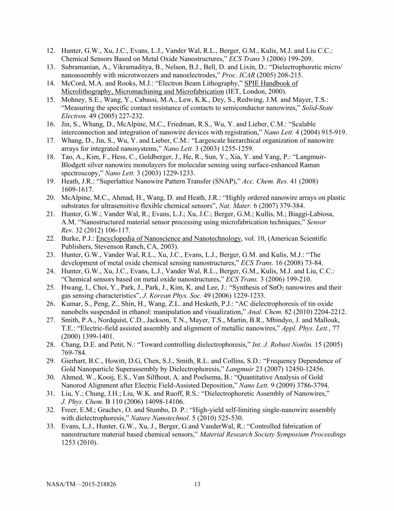
References 1. Hunter, G.W. et al.: “Development of Chemical Sensor Arrays for Harsh Environments and
Aerospace Applications,” Proc. IEEE Sensors 2 (2002) 1126-1133. 2. Hunter, G.W.; Xu J.C. and Makel, D.B.: BioNanoFluidic MEMS (Springer Science and Business
Media, New York, 2008). 3. Batzill, M. and Diebold, U.: “The surface and materials science of tin oxide,” Prog. Surf. Sci 79
(2005) 47-154. 4. Rothschild, A. and Komem, Y.: “The effect of grain size on the sensitivity of nanocrystalline metal-
oxide gas sensors,” J. Appl. Phys. 95 (2004) 6374-6380. 5. Shen, G.; Chen, P.C.; Ryu, K. and Zhou, C.: “Devices and chemical sensing applications of metal
oxide nanowires,” J. Mater. Chem. 19 (2009) 828-839. 6. Gurlo, A.: “Nanosensors: towards morphological control of gas sensing activity. SnO2, In2O3, ZnO
and WO3 case studies,” Nanoscale 3 (2011) 154-165. 7. Hunter, G.W.; Xu, J.C.; Biaggi-Labiosa, A.M.; Laskowski, D.; Dutta, P.K.; Mondal, S.P.; Ward,
B.J.; Makel, D.B.; Liu, C.C.; Chang, C.W. and Dweik, R.A.: “Smart sensor systems for human health breath monitoring applications,” J. Breath Res. 5 (2011) 037111.
8. Choi, Y.J.; Hwang, I.S.; Park, J.G.; Chpi, K.J.; Park, J.H. and Lee, J.H.: “Novel fabrication of an SnO2 nanowire gas sensor with high sensitivity,” Nanotechnology 19 (2008) 095508.
9. Comini, E., Faglia, G., Sberveglieri, G., Pan, Z. and Wang, Z.L.: “Stable and highly sensitive gas sensors based on semiconducting oxide nanobelts,” Appl. Phys. Lett. 81 (2002) 1869-1871.
10. Fan, Z. and Lu, J.G.: “Zinc oxide nanostructures: synthesis and properties,” J. Nanosci. Nanotechnol. 5 (2005)1561-1573.
11. Ponzoni, A., Comini, E., Sberveglieri, G., Zhou, J., Deng, S.Z., Xu, N.S., Ding, Y. and Wang, Z.L.: “Ultrasensitive and highly selective gas sensors using three-dimensional tungsten oxide nanowire networks,” Appl. Phys. Lett. 88 (2006) 203101-203103.
NASA/TM—2015-218826 13
12. Hunter, G.W., Xu, J.C., Evans, L.J., Vander Wal, R.L., Berger, G.M., Kulis, M.J. and Liu C.C.: Chemical Sensors Based on Metal Oxide Nanostructures,” ECS Trans 3 (2006) 199-209.
13. Subramanian, A., Vikramaditya, B., Nelson, B.J., Bell, D. and Lixin, D.: “Dielectrophoretic micro/ nanoassembly with microtweezers and nanoelectrodes,” Proc. ICAR (2005) 208-215.
14. McCord, M.A. and Rooks, M.J.: “Electron Beam Lithography,” SPIE Handbook of Microlithography, Micromachining and Microfabrication (IET, London, 2000).
15. Mohney, S.E., Wang, Y., Cabassi, M.A., Lew, K.K., Dey, S., Redwing, J.M. and Mayer, T.S.: “Measuring the specific contact resistance of contacts to semiconductor nanowires,” Solid-State Electron. 49 (2005) 227-232.
16. Jin, S., Whang, D., McAlpine, M.C., Friedman, R.S., Wu, Y. and Lieber, C.M.: “Scalable interconnection and integration of nanowire devices with registration,” Nano Lett. 4 (2004) 915-919.
17. Whang, D., Jin, S., Wu, Y. and Lieber, C.M.: “Largescale hierarchical organization of nanowire arrays for integrated nanosystems,” Nano Lett. 3 (2003) 1255-1259.
18. Tao, A., Kim, F., Hess, C., Goldberger, J., He, R., Sun, Y., Xia, Y. and Yang, P.: “Langmuir-Blodgett silver nanowire monolayers for molecular sensing using surface-enhanced Raman spectroscopy,” Nano Lett. 3 (2003) 1229-1233.
19. Heath, J.R.: “Superlattice Nanowire Pattern Transfer (SNAP),” Acc. Chem. Res. 41 (2008) 1609-1617.
20. McAlpine, M.C., Ahmad, H., Wang, D. and Heath, J.R.: “Highly ordered nanowire arrays on plastic substrates for ultrasensitive flexible chemical sensors”, Nat. Mater. 6 (2007) 379-384.
21. Hunter, G.W.; Vander Wal, R.; Evans, L.J.; Xu, J.C.; Berger, G.M.; Kullis, M.; Biaggi-Labiosa, A.M. “Nanostructured material sensor processing using microfabrication techniques,” Sensor Rev. 32 (2012) 106-117.
22. Burke, P.J.: Encyclopedia of Nanoscience and Nanotechnology, vol. 10, (American Scientific Publishers, Stevenson Ranch, CA, 2003).
23. Hunter, G.W., Vander Wal, R.L., Xu, J.C., Evans, L.J., Berger, G.M. and Kulis, M.J.: “The development of metal oxide chemical sensing nanostructures,” ECS Trans. 16 (2008) 73-84.
24. Hunter, G.W., Xu, J.C., Evans, L.J., Vander Wal, R.L., Berger, G.M., Kulis, M.J. and Liu, C.C.: “Chemical sensors based on metal oxide nanostructures,” ECS Trans. 3 (2006) 199-210.
25. Hwang, I., Choi, Y., Park, J., Park, J., Kim, K. and Lee, J.: “Synthesis of SnO2 nanowires and their gas sensing characteristics”, J. Korean Phys. Soc. 49 (2006) 1229-1233.
26. Kumar, S., Peng, Z., Shin, H., Wang, Z.L. and Hesketh, P.J.: “AC dielectrophoresis of tin oxide nanobelts suspended in ethanol: manipulation and visualization,” Anal. Chem. 82 (2010) 2204-2212.
27. Smith, P.A., Nordquist, C.D., Jackson, T.N., Mayer, T.S., Martin, B.R., Mbindyo, J. and Mallouk, T.E.: “Electric-field assisted assembly and alignment of metallic nanowires,” Appl. Phys. Lett., 77 (2000) 1399-1401.
28. Chang, D.E. and Petit, N.: “Toward controlling dielectrophoresis,” Int. J. Robust Nonlin. 15 (2005) 769-784.
29. Gierhart, B.C., Howitt, D.G, Chen, S.J., Smith, R.L. and Collins, S.D.: “Frequency Dependence of Gold Nanoparticle Superassembly by Dielectrophoresis,” Langmuir 23 (2007) 12450-12456.
30. Ahmed, W., Kooij, E.S., Van Silfhout, A. and Poelsema, B.: “Quantitative Analysis of Gold Nanorod Alignment after Electric Field-Assisted Deposition,” Nano Lett. 9 (2009) 3786-3794.
31. Liu, Y.; Chung, J.H.; Liu, W.K. and Ruoff, R.S.: “Dielectrophoretic Assembly of Nanowires,” J. Phys. Chem. B 110 (2006) 14098-14106.
32. Freer, E.M.; Grachev, O. and Stumbo, D. P.: “High-yield self-limiting single-nanowire assembly with dielectrophoresis,” Nature Nanotechnol. 5 (2010) 525-530.
33. Evans, L.J., Hunter, G.W., Xu, J., Berger, G.and VanderWal, R.: “Controlled fabrication of nanostructure material based chemical sensors,” Material Research Society Symposium Proceedings 1253 (2010).

NASA/TM—2015-218826 14
34. Evoy, S.; DiLello, N.; Deshpande, V.; Narayanan, A.; Liu, H.; Riegelman, M.; Martin, B.R.; Hailer, B.; Bradley, J.C.; Weiss, W.; Mayer, T.S.; Gogotsi, Y.; Bau, H.H.; Mallouk, T.E. and Raman, S.: “Dielectrophoretic assembly and integration of nanowire devices with functional CMOS operating circuitry,” Microelectron. Eng. 75 (2004) 31-42.
35. Biaggi-Labiosa, A.M.; Solá, F.; Lebrón-Colón, M.; Evans, L.J.; Xu, J.C.; Hunter, G.W.; Berger, G.M. and González, J.M.: “A novel methane sensor based on porous SnO2 nanorods: room temperature to high temperature detection,” Nanotechnology 23 (2012) 455501.
36. NanoLab Inc., Waltham, MA, http://www.nano-lab.com/home.html. 37. Microposit S1805 Photoresist, Shipley Company, Marlborough, MA.