Embed Size (px)
Citation preview

Integration, the VLSI Journal 72 (2020) 39–57
Contents lists available at ScienceDirect
Integration, the VLSI Journal
journal homepage: www.elsevier.com/locate/vlsi
Defense-in-depth: A recipe for logic locking to prevail
M. Tanjidur Rahman a, M. Sazadur Rahman a, Huanyu Wang a, Shahin Tajik a, Waleed Khalil b,Farimah Farahmandi a, Domenic Forte a, Navid Asadizanjani a,**, Mark Tehranipoor a,*
a Florida Institute for Cybersecurity (FICS) Research, Electrical & Computer Engineering Department, University of Florida, Gainesville, FL, USAb Electrical & Computer Engineering Department, Ohio State University, OH, USA
A R T I C L E I N F O
Keywords:Logic obfuscationTamper-proof memoryScan chainOracle-guided attackPhysical attack
* Corresponding author.** Corresponding author.
E-mail addresses: [email protected] (N. Asadiz
https://doi.org/10.1016/j.vlsi.2019.12.007Received 19 July 2019; Received in revised form 1Available online 11 January 20200167-9260/© 2019 Elsevier B.V. All rights reserved
A B S T R A C T
Logic locking/obfuscation has emerged as an auspicious solution for protecting the semiconductor intellectualproperty (IP) from the untrusted entities in the design and fabrication process. Logic locking disguises theimplementation and functionality of the IP by implanting additional key-gates in the circuit. The right output ofthe locked chip is produced, once the correct key value is available at the input of the key-gates. The confi-dentiality of the key is imperative for the security of the locked IP as it stands as the lone barrier against IPinfringement. Therefore, the logic locking is considered as a broken scheme once the key value is exposed. Thelogic locking techniques have shown vulnerability to different classes of attacks, such as Oracle-guided andphysical attacks. Although the research community has proposed a number of countermeasures against suchattacks, none of them is simultaneously unbreakable against Oracle-guided, Oracle-less, and physical attacks.Under such circumstances, a defense-in-depth mechanism can be considered as a feasible approach in addressingthe vulnerabilities of logic locking. Defense-in-depth is a multilayer defense strategy where several independentcountermeasures are implemented in the device to provide aggregated protection against different attack vectors.
Introducing such a multilayer shielding model in logic locking is the major contribution of this paper. Withregard to this, we first identify the core components of logic locking schemes, which need to be protected. Af-terwards, we categorize the vulnerabilities of core components according to potential threats for the locking keyin logic locking schemes. Furthermore, we propose several defense layers and countermeasures to protect thedevice from those vulnerabilities. In conclusion, we believe that a logic locking technique with a layered defensemechanism can be a possible solution against IP piracy.
1. Introduction
Over the past two decades, the business model for the semiconductorindustry has shifted from vertical to horizontal. In the horizontal model,the original component manufacturers (OCM) outsource different stepsof the chip manufacturing process, like intellectual property (IP) design,fabrication, and design-for-test (DFT) structure insertion, to more so-phisticated offshore fabrication facilities. This approach makes themanufacturing process less expensive for new technology developmentand scaling down the existing IPs. However, due to the number ofstakeholders involved in design, integration, manufacturing, and distri-bution located around the globe, the OCM and IP owner/vendor have lostcontrol over the supply chain. As a result, IP piracy, counterfeiting,reverse engineering, and hardware Trojan insertion have becomeeminent threats in the semiconductor industry. The conventional passive
anjani), [email protected]
6 October 2019; Accepted 18 De
.
IP protection methods, e.g., patents and copyrights, provide no protec-tion against the aforementioned threats. Researchers have proposedseveral hardware obfuscation techniques, such as logic locking/obfus-cation [1], state space obfuscation [2], and IC camouflaging [3] as anactive approach for safeguarding the IP.
Hardware obfuscation is a method of transforming the design andlayout of the IP while maintaining the original functionality of it. Amongthe hardware obfuscation techniques, logic locking is appearing aspossible solutions for establishing trust in the hardware design. In logiclocking, additional combinational logic gates [1] or state spaces [2] areinserted in the design to protect the implementation and functionality ofthe IP from exposing. Logic Locking is a key-based hardware obfuscationapproach and the inserted logic elements are generally termed as key--gates. The output of the chip is unlocked once the key-gates are connectedto the unlocking key-sequence which configured by the IP owner or OCM
(M. Tehranipoor).
cember 2019
M.T. Rahman et al. Integration, the VLSI Journal 72 (2020) 39–57
through a non-volatile (NVM) memory after the chip is fabricated.Although logic locking appeared as a promising protection mecha-
nism against IP piracy, the literature shows that this approach is sus-ceptible to several Oracle-guided attacks [4], like Boolean Satisfiability(SAT) attacks [5,6], Signal Probability Skey (SPS) attacks [7] and keysensitization attacks [8]. Over the last few years, Oracle-less attacks havealso proved to be successful in key extraction [9,10]. Over the pastseveral years, the security community has focused on developing coun-termeasures to hinder those Oracle-guided attacks [11,12]. Althoughprotection against the above-mentioned attacks received a lot of atten-tion, unfortunately, the security of the key itself is still ignored. Thereason for such ignorance is lying under the two common assumptionsmade in those aforementioned attacks. First, as the untrusted foundrydoes not possess the key during fabrication and has only access to thelocked netlist/layout and the scan chain, implemented as DFT, onlyOracle-guided are considered as the most acceptable method of keyextraction. Second, the unlocking key is written into a tamper- andread-proof memory, and therefore, is protected against reverse engi-neering in the field. However, an adversary such as an untrusted foundrywith access to most advanced failure analysis (FA) equipment, such asmicroprobing station, scanning electron microscope (SEM) and laserscanning microscope (LSM), should be more than capable of extractingthe unlocking key from a chip by contact-based electrical [13,14] orcontactless optical probing [15]. Furthermore, the literature on logiclocking does not consider the threat imposed by an end user withfull-blown reverse engineering capability [16] and an untrusted 3rdparty design service provider [17,18] in the supply chain. The task of areverse engineer can be made difficult through implementing physicallayout obfuscation techniques like camouflage cells, dummy vias, fillercells, etc. in the chip [3,19]. However, the aforementioned layoutobfuscation methods do not eliminate the threat of IP piracy by reverseengineering. Thus, key-based obfuscation techniques are less secureagainst physical attacks than previously thought due to the possibili-ty/ease of key extraction. As a result, after nearly a decade of research,none of the logic locking techniques are able to provide absolute defenseagainst IP piracy/theft and root-of-trust violation.
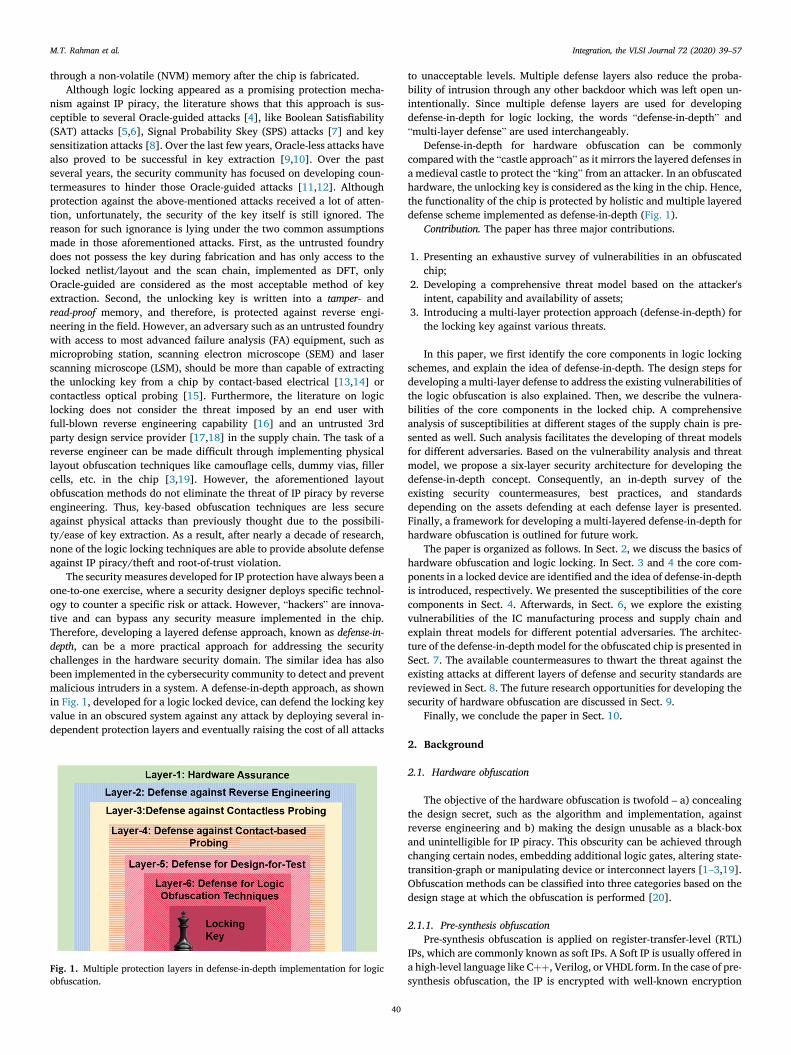
The security measures developed for IP protection have always been aone-to-one exercise, where a security designer deploys specific technol-ogy to counter a specific risk or attack. However, “hackers” are innova-tive and can bypass any security measure implemented in the chip.Therefore, developing a layered defense approach, known as defense-in-depth, can be a more practical approach for addressing the securitychallenges in the hardware security domain. The similar idea has alsobeen implemented in the cybersecurity community to detect and preventmalicious intruders in a system. A defense-in-depth approach, as shownin Fig. 1, developed for a logic locked device, can defend the locking keyvalue in an obscured system against any attack by deploying several in-dependent protection layers and eventually raising the cost of all attacks
Fig. 1. Multiple protection layers in defense-in-depth implementation for logicobfuscation.
40
to unacceptable levels. Multiple defense layers also reduce the proba-bility of intrusion through any other backdoor which was left open un-intentionally. Since multiple defense layers are used for developingdefense-in-depth for logic locking, the words “defense-in-depth” and“multi-layer defense” are used interchangeably.
Defense-in-depth for hardware obfuscation can be commonlycompared with the “castle approach” as it mirrors the layered defenses ina medieval castle to protect the “king” from an attacker. In an obfuscatedhardware, the unlocking key is considered as the king in the chip. Hence,the functionality of the chip is protected by holistic and multiple layereddefense scheme implemented as defense-in-depth (Fig. 1).
Contribution. The paper has three major contributions.
1. Presenting an exhaustive survey of vulnerabilities in an obfuscatedchip;
2. Developing a comprehensive threat model based on the attacker'sintent, capability and availability of assets;
3. Introducing a multi-layer protection approach (defense-in-depth) forthe locking key against various threats.
In this paper, we first identify the core components in logic lockingschemes, and explain the idea of defense-in-depth. The design steps fordeveloping a multi-layer defense to address the existing vulnerabilities ofthe logic obfuscation is also explained. Then, we describe the vulnera-bilities of the core components in the locked chip. A comprehensiveanalysis of susceptibilities at different stages of the supply chain is pre-sented as well. Such analysis facilitates the developing of threat modelsfor different adversaries. Based on the vulnerability analysis and threatmodel, we propose a six-layer security architecture for developing thedefense-in-depth concept. Consequently, an in-depth survey of theexisting security countermeasures, best practices, and standardsdepending on the assets defending at each defense layer is presented.Finally, a framework for developing a multi-layered defense-in-depth forhardware obfuscation is outlined for future work.
The paper is organized as follows. In Sect. 2, we discuss the basics ofhardware obfuscation and logic locking. In Sect. 3 and 4 the core com-ponents in a locked device are identified and the idea of defense-in-depthis introduced, respectively. We presented the susceptibilities of the corecomponents in Sect. 4. Afterwards, in Sect. 6, we explore the existingvulnerabilities of the IC manufacturing process and supply chain andexplain threat models for different potential adversaries. The architec-ture of the defense-in-depth model for the obfuscated chip is presented inSect. 7. The available countermeasures to thwart the threat against theexisting attacks at different layers of defense and security standards arereviewed in Sect. 8. The future research opportunities for developing thesecurity of hardware obfuscation are discussed in Sect. 9.
Finally, we conclude the paper in Sect. 10.
2. Background
2.1. Hardware obfuscation
The objective of the hardware obfuscation is twofold – a) concealingthe design secret, such as the algorithm and implementation, againstreverse engineering and b) making the design unusable as a black-boxand unintelligible for IP piracy. This obscurity can be achieved throughchanging certain nodes, embedding additional logic gates, altering state-transition-graph or manipulating device or interconnect layers [1–3,19].Obfuscation methods can be classified into three categories based on thedesign stage at which the obfuscation is performed [20].
2.1.1. Pre-synthesis obfuscationPre-synthesis obfuscation is applied on register-transfer-level (RTL)
IPs, which are commonly known as soft IPs. A Soft IP is usually offered ina high-level language like Cþþ, Verilog, or VHDL form. In the case of pre-synthesis obfuscation, the IP is encrypted with well-known encryption

M.T. Rahman et al. Integration, the VLSI Journal 72 (2020) 39–57
techniques, e.g., IEEE P1735 [21]. Obfuscating the RTL code with a finitestate machine (FSM) has also been proposed, where the code later tra-versed with a key sequence or code-word [20]. The design house acquiresa pre-synthesized IP from IP vendors and uses it in a design as a“black-box”. However, protecting the obfuscating key sequence from themalicious entity in the supply chain is still appear as a challenge for thesecurity community.
2.1.2. Post-synthesis obfuscationPost-synthesis obfuscation is the method of hiding the true func-
tionality of the device under attack (DUA) through structural modifica-tions in the design.
The insertion of additional logic elements, interconnects, or modifi-cations in the FSM are prevalent examples of structural modifications inthe post-synthesis obfuscation. Combinational logic locking and FSMlocking are two most researched post-synthesis obfuscation methods inthe literature.
2.1.3. Physical layout obfuscationThe objective of physical layout obfuscation is to thwart the IP reverse
engineering and prevent any malicious modifications in the layout. Inthis method, the physical characteristics of the circuit or the layout ismodified to increase ambiguity in cell identification or connectivity.Several techniques have been proposed for layout obfuscation, such asdoping based techniques, and dummy contact insertion in the fabricationlevel [22]. The layout can also be hidden at the cell level using camou-flaging cells [3]. Camouflage cells alter the layout of two standard cellswith different functionalities to appear identical. Camouflage cells can bedeveloped using real and dummy contacts. As shown in Fig. 2a and 2b,2-input NAND and NOR gates can be differentiated through analyzing theactive region and metal layers. These two gates can be made lookedidentical (Fig. 2c and 2d) by introducing dummy vias. Inserting dummygates, dummy filler metal or manipulating doping implant have also beenused to generate camouflage cells [19,23,24]. The insertion of dummyvias and identical logic gates introduce ambiguity in image processingbased reverse engineering. However, camouflage cells introduce area,power, and delay overhead in the design [25]. In the case of gate-levelobfuscation, camouflage cell insertion algorithms [3] have been pro-posed. Camouflage connections [23]. vanishing vias [26], timingcamouflaging [27], and flip-flop obfuscation [28] have also been pro-posed to prevent reverse engineering.
2.2. Logic locking
Logic locking or logic obfuscation is developed to hide the function-ality of an IP by inserting additional logic gates into the netlist of IP. Suchprotection is provided through embedding additional logic gates into thecombinational or sequential parts of the design (Fig. 3). While the former
Fig. 2. The camouflage gates described in Ref. [3]. Standard NAND gate (a) and NOlayers. Camouflaged NAND gate (c) and NOR gate (d). These gates have identical to
41
approach is called combinational logic locking, the latter is called FSMlocking. In the case of combinational logic locking, the extra embeddedlogic gates are known as key-gates, which are connected to primary inputsthat are collectively referred to as the key. On the other hand, in FSMlocking approaches, the functionality of the IP is obscured with addi-tional states in the state transition graph [2]. Applying a correct sequenceof the key, an authorized user can initiate the functional state of theIP/chip. In both techniques, the design provides the correct functionalityonly if the provided key-input values are correct. Otherwise, the IP doesnot reveal correct input-output behaviour. The key value is only availableto the OCM and the IP owner and not available during the fabricationprocess. Therefore, once the chips are fabricated, they are transferred to atrusted facility for programming the key, known by the design house, intoa secure and tamper-proof key-storage element. In the case of combina-tional logic locking, it has already been shown that random insertion ofkey-gates may not add a significant security feature to the design [29].Therefore, several key-gate insertion algorithms, like the insertion ofXOR/XNOR gates [1,29], lookup tables [30], and multiplexers [29] havebeen proposed. Furthermore, Shamsi et al. [31] defined the problem oflocking a circuit (e.g., logic locking, camouflaging, andsplit-manufacturing) as a translational function to the original circuit,which is obscure without a secret key. They defined several notions ofsecurity for this translational function under different adversary models.
3. Core components in an obfuscated IC
In this section, we discuss the core components of a locked device.Each component is defined by its functions and involvement in the se-curity of the device. An IC implemented with either combinational orsequential logic locking have five imperative components – (a) Key-storage element; (b) Key-delivery unit; (c) Interconnects; (d) Design-for-test; (e) Obfuscated hardware.
3.1. Key-storage element
In logic locking, after the fabrication, the ICs are transferred to atrusted facility for configuring the key into a secure and tamper-proofkey-storage element (see Fig. 4). As the key is essential for the correctfunctionality of the device, storing the key in volatile memory is notsuitable for such a purpose. In the case of a volatile key-storage, keepingthe chip in a continuous power-up state to maintain the stored value isnot a practical approach in terms of power consumption [32]. Therefore,non-volatile memories (NVMs) and one-time programmable (OTP)memories are the conventional choice as key storage elements.
3.2. Interconnects
Interconnects are the metal wires in the chip which connect different
R gate (b). These gates could be easily differentiable by looking at the top metalp metal layers and are. therefore, harder to identify.

Fig. 3. Simplified example of logic locking method.
Fig. 4. Core components in an IC implemented with hardware obfuscation.
M.T. Rahman et al. Integration, the VLSI Journal 72 (2020) 39–57
elements, like transistors, capacitors, etc. and naturally more complexmodules, such as memory, processors, cache, etc. in the chip. Dependingon the functionality and complexity of the IC, the number of interconnectlayers may vary. All devices exchange confidential data between memoryand other operational units in the chip through interconnects. Forexample, The obfuscation keys and other security-critical assets, such asencryption keys, device configuration, and manufacturer firmware aretypically stored in a key-storage memory cells. Therefore, these memorycells storing the assets are the root of the security for the design, whichneeds exclusive protections, such as memory encryption techniques.However, to process the assets in the logic, they have to be transmitted tothe logic parts of the chip through chip interconnects. Hence, protectingthe interconnects against potential vulnerabilities, such as probing andbus snooping, is equally important in logic obfuscation schemes.
3.3. Key-delivery unit
The key value is compulsory for the operation of the correspondingkey-based obfuscated IP. Hence, initialization of any IP must includereading the locking key from the key-storage element. Thereafter, the keymust be fed to the key-gates through registers connected to those key-gates [16,33]. These registers, which can be termed as key-registers,should be privileged registers to prevent any inadvertent manipulationof key values and should maintain the stored data during the entireoperating period of the IP/chip. The key can be fed directly to thekey-gates from the key-storage. However, it does not eliminate therequirement for a read-circuitry, which is also considered in thekey-delivery unit, connected to the key-storage. In addition, the confi-dentiality of the locking key requires to be maintained by digital rightmanagement (DRM) policies [34,35]. Moreover, the unlocking key canalso be stored in an encrypted format in the key-storage [1]. Theencrypted keymust be decrypted before fed to the key-gates. This impliesthe involvement of a decryption engine. Furthermore, reading the keyfrom secured storage may include key-management logic in the chip forcryptomodules as described in Ref. [36]. All the key-read circuitry,key-registers, and key-management logic establish the key delivery unit
42
for a locked device and should be protected against asset leakage.
3.4. Design-for-Test
Design-for-Test techniques are widely used in modern system-on-chips(SoCs) to ensure testability of internal circuit elements for monitoring thereliability of the hardware design. This added feature makes it easier toperform structural tests in the hardware design. The manufacturingprocess is not perfect, making post-silicon validation of designed hard-ware a vital one. The purpose of functional tests is to verify the correctfunctionality of the hardware design. However, functional tests are veryexpensive and the complexity of applying them is too high to realize. Tocircumvent this obstacle, additional DFT logic is added in the circuit toovercome the difficulty of functional testing in a divide and conquerfashion. For all these obvious reasons, we are considering DFT as a corecomponent in an obfuscated IC. Design-for-test can be inserted in thedesign by replacing sequential memory elements with scan cells andconverting a sequential design into a combinational one to facilitate thestructural testing process. However, these scan cells can be used to attackobfuscated hardware designs to extract keys, e.g., key sensitization andOracle-based attacks.
3.5. Obfuscated hardware
The last core element for the security of the chip is the obfuscatedhardware. The functionality and layout of the chip can be concealed froman adversary by implementing different logic locking and physicalobfuscation techniques. Depending on the objective of the hardwareobfuscation, the obfuscation techniques can be applied in three ways:
3.5.1. Device-level hardware obfuscationAt the device level, the layout of the device is disguised by intro-
ducing stuck-at-fault or delay manipulation [37]. Changes in dopingconcentration, manipulating inter-layer dielectric, inserting dummy logicand interconnects are conventional techniques to achieve a device-levelobfuscated hardware.
3.5.2. Circuit-level hardware obfuscationThe circuit-level hardware obfuscation focuses on hiding the gate
functionality by modifying cell libraries [37]. Camouflage cells, fillercell, dummy vias, and dummy interconnects are examples of circuit-levelobfuscation.
3.5.3. System-level or gate-level hardware techniqueLogic locking techniques, i.e., combinational logic locking and FSM
locking are considered as system-level or gate-level obfuscation tech-niques. The algorithms used for structural and physical obfuscationmethods are also considered as system-level techniques for obfuscatingthe chip design.

M.T. Rahman et al. Integration, the VLSI Journal 72 (2020) 39–57
4. Defense-in-depth
4.1. Motivation and definition of defense-in-depth
The vulnerabilities of core components leave a wide attack surfaceavailable for different adversaries to extract the assets, i.e., the lockingkey, layout, and design implementation, from the IC. Naturally, a singledefensive mechanism against a specific vulnerability cannot protect thefunctionality and design of the chip against all potential threats. Once anattacker bypasses the only defensive mechanism implemented in thechip, the security of the entire lockingmechanism is broken. For instance,developing mitigation against oracle-guided attacks, namely SAT attacks,cannot defend against the threat of physical attacks, like optical andelectrical probing. As a result, multiple layers of countermeasures shouldbe implemented to provide protection for the IP/chip against a widerange of attack vectors. Such a multi-layer defense approach is identifiedas defense-in-depth. In this paper, we present the defense-in-depth modelwhere different layers of security system address different vulnerabilitiesof core components.
4.2. Developing the model for defense-in-depth
Developing a model for in-depth defense mechanism for logicobfuscation requires a complex set of analysis on interconnections anddependencies between the different aspects of the supply chain, threatmodel, system design, protection mechanism, and assets. Besides,providing effective monitoring and protection is required for mitigatingthe attacks on the IC. Developing a defense-in-depth model for hardwareobfuscation can be compiled in four stages as shown in Fig. 5;
1. Security Analysis of Core Components: The first step for modeling thedefense-in-depth is identifying the vulnerabilities that are present inthe core components of logic locking. The assets and methodologiesof extracting key and design implementation from an obscured chip,i.e., the attack surface of the IC is identified at this stage.
2. Threat Model Analysis: In developing countermeasures and standardsfor protecting IPs from piracy, overbuilding, or hardware Trojaninsertion, the capability of the adversary has been critically under-estimated. An attacker can exploit any existing vulnerability in thedesign which may remain undetected for a long period of time.Therefore, assessing the roles of the stakeholders in the supply chainfacilitates in identifying the presence of potential adversaries in thesupply chain. The attack surface can also be defined using thevulnerability analysis of supply chain. Analyzing the capabilities,goals of an adversary, and availability of assets is another dimensionfor selecting the attack methodology and significantly influence thedefense-in-depth modeling.
3. Developing the Defense-in-Depth Architecture: At this stage, the designerdefines the defense layers that protect the chip assets (for example,the defense-in-depth layers depicted in Fig. 1) based on the vulner-abilities of core components, the threat model, desired level of se-curity and design budget allocated for the security of the designsecrets. In addition, a designer should consider that, a malicious en-tity can gain unauthorized access to design assets through the simpleshortcomings in the design architecture perimeter, or embedded ca-pabilities in the design that are forgotten, unnoticed, or simply
Fig. 5. Steps for developing a defense
43
disregarded. Therefore, a multi-layer defense approach must addressthe protection for the aforementioned ‘backdoors’ in the device.
4. Security Standards and Selection of Countermeasures: The next step fordeveloping defense-in-depth is to identify the effective countermea-sures and protection schemes for protecting core components fromthe adversary. Design budget, i.e., area, power, and energy, defined atthe architecture stage plays definitive role in the selection ofcountermeasures.
5. Security Analysis of Core Components
Although most research efforts have been confined to protect theobfuscated SoC by improving the security of obfuscated hardware andDFT, a comprehensive study about the possible vulnerabilities of othercore elements in hardware obfuscation is still absent in the literature. Inthis section, we will discuss the vulnerabilities of the core elements in anobfuscated device.
5.1. Vulnerabilities of the key-storage element
Protecting the key-storage element is vital for logic locking schemessince the exposure of unlocking key breaks the security of the entirescheme. NVM and OTP memories are considered as possible key-storagecandidates in logic locking schemes. NVMs, like ROM, EEPROM, andFlash, are the prominent candidates for key-storage. The NVM can berealized as off-chip or on-chip memory. As off-chip memory is vulnerableto data interception attack at chip boundary, on-chip NVM is the onlysuitable choice as secure key storage. Although aforementioned memorytechnologies are widely deployed by the industry as secure and tamper-proof memories, the main vulnerability of NVM is the availability of thedata stored in the memory during the power-off state. In this state, thememory remains defenseless against any tampering attack. Therefore, anadversary can deploy advanced FA tools to reverse engineer the memoryand readout its contents.
Another option for securing key-storage is OTP memory, such asROM, electric fuse (eFuse) and antifuse. OTP memory facilitates toconfigure the device before shipping to the end user once the chip isfabricated. eFuse is a continuous metal or polysilicon shape etched on thesilicon surface. An eFuse structure is shown in Fig. 6a. When a voltage isapplied to the eFuse, electromigration causes the open circuit in the cell(the broken fuse in Fig. 6a) and program the eFuse [38]. An attacker withaccess to FA tools can deprocess the entire die and locate the location ofeFuse. Later, using the SEM, she can differentiate between the pro-grammed and unprogrammed eFuse link by observing the metal or sili-cide link of the eFuse. Similar information can be extracted usingelectrical probing [13,41]. On the other hand, due to scalability into 7 nmnode technology, relatively smaller antifuse cells appear as rising solu-tions to key-storage element. Antifuse is a standard CMOS transistorwhich acts as a high resistance in its unprogrammed state. Once electricalstress is applied to the gate oxide of the transistor (see Fig. 6b), thetransistor acts as a low resistance conductive path. Antifuse can also beplaced as via between two metal lines in the chip. In such a case,detecting the location of antifuse is difficult with SEM imaging. SEMprovides information about the die surface, i.e., the XY plane of the die.However, the lateral information of the metal layers in the die is requiredto distinguish the antifuse fabricated as via. The lateral information of themetal layers can only be observed by transmission electron microscopy
-in-depth model for logic locking.

Fig. 6. (a) Difference between before and after program of a TSMC eFuse structure in Qualcomm Gobi MDM9235 Modem 20 nm HKMG [38]; (b) 1T-Fuse Bit Cell inDesignWare OTP NVM IP. The cell is programmed by applying a controlled, irreversible breakdown voltage from the gate through the core (gate) oxide to the channel[39]; (c) Key process steps for 3D Nand fabrication process [40].
Fig. 7. (a) FIB deposits Platinum in the milling cavity to build a conducting path(green) from the target wire; (b) The deposited conducting path serves as aelectrical pad for the probe contact [47]. (For interpretation of the references tocolor in this figure legend, the reader is referred to the Web version ofthis article.)
M.T. Rahman et al. Integration, the VLSI Journal 72 (2020) 39–57
(TEM). As sample preparation and imaging for TEM are more challengingthan SEM, differentiating between the programmed and unprogrammedbits is difficult but not impossible for antifuse. However, once the loca-tion of anti-fuse is extracted the stored bit can be probed. Moreover, allthe OTPs require higher breakdown voltage and a large peripheral cir-cuit, which introduces area overhead and higher power consumption[32].
Other conventional examples of NVMs are EEPROM and Flashmemories. Each EEPROM cell has two transistors - a floating gate orstorage transistor and a select transistor. The storage transistor has afloating gate which traps the electrons. A Flash cell only has the floatinggate transistor and uses the same logic storage mechanism as EEPROM.Since both memory technologies use stored charges in the floating gatefor storing the bit values, any attempt to image the memory cell with SEMor TEM can disturb the charges distribution and possibly erase thememory content. Therefore, reverse engineering of such NVMs has al-ways been considered as a challenging task; even after the recent ad-vancements in FA tools. Nardi et al. [42] solved the challenge ofmaintaining the value of stored charge by accessing the memory from theback-side of IC. Once an attacker gets access to the floating gates ofEEPROM/Flash, she can use scanning Kelvin probe microscopy (SKPM),scanning probe microscopy (SPM), passive voltage contrast (PVC) orscanning capacitancemicroscopy (SCM) for extracting the stored value inthe EEPROM/Flash [42,43]. However, the security of the 3D Flash chips(see 3D NAND flash cells in Fig. 6c) have yet to be investigated. In the 3Dflash technology, the memory cells, previously organized horizontally,are now stacked vertically and connected with pillar and channels.Although such orientation requires further precaution during polishingthe back-side of the chip and PVC analysis, the reverse engineering of 3DNAND memory is, in principle, still possible.
Physical unclonable functions (PUFs), as other possible candidates forsecure key-storage, was developed to generate keys from intrinsic prop-erties of the device [44]. Although PUF has been assumed to betamper-evident against physical attacks, they have demonstrated vul-nerabilities against several non- and semi-invasive attacks, like photonicemission analysis and laser fault injection [44] Furthermore, theresponse of PUF differs for each chip due to process variation whichmakes it incompatible for ASIC design, where the same mask would beused for fabricating all the chip in the same batch. On the other hand,storing the key value in the battery-backed RAM also does not add anysignificant security feature to the key-storage as they can be read outthrough optical attacks, such as thermal laser stimulation (TLS) [45].
Data remanence in key-storage like NVM and RAM is another class ofvulnerability for all key-storage elements. Data remanence is the residualphysical representation (e.g., the trapped charge or voltage) of the datathat has been erased from the memory during a tampering attack orregular operation of the chip. A tamper-sensor enclosure can initiate theerasure procedure for memory if the tampering event is detected. Thesensor connects the memory to the ground to zeroized the stored data.
44
However, due to data remanence effect, an attacker can exploit the re-sidual property of the memory to extract the content of the memory. Thedata remanence vulnerability occurs when data retention time exceedsthe time required by a malicious entity to read out or dump the storedvalue in another memory location. Consequently, the protection mech-anism can be defeated [46].
5.2. Vulnerabilities of the interconnects
Sensitive information transmitted on wires in ICs can be physicallyextracted using contact-based electrical probing attack [13]. In this typeof attack, the chip's wires are contacted by a probe, and as a result, thesignal carried by the wires can be read out when the chip is functioning.Therefore, electrical probing is considered as a contact-based method forextracting the assets in the chip. Electrical probing attacks can be clas-sified into frontside probing, which is carried out through the passivationlayer and upper metal layers, and back-side probing, which is mountedthrough the silicon substrate.
Due to the large size of probes in comparison to the size of metals’width and available space between wires, the frontside electrical probingis a challenging task. To overcome these limitations, attackers usuallydeploy focused ion beam (FIB), which is a powerful tool commonly usedin the testing, development, and editing of ICs with nanoscale precision,to mill a narrow cavity, get access to the target wire on lower metallayers, and build a conducting path without damaging upper metal layersas shown in Fig. 7. Modern FIB systems, such as ZEISS.
ORION NanoFab, can edit out obstructing circuitry with a 5 nmprecision. FIB aspect ratio is a key feature of FIB's capability, which isdefined as the ratio between the depth and diameter of the milling cavity.

M.T. Rahman et al. Integration, the VLSI Journal 72 (2020) 39–57
Thus, the higher of the FIB aspect ratio, the thinner of the milling cavity,the less probability to damage signal wires on the chip, and the highersuccess rate to extract wire values.
Some high-security level chips, such as smart cards, may have shield-like mechanisms to protect the chip against frontside probing attacks.However, this type of countermeasure may still be compromised bybypass and reroute attacks [13] using advanced FIBs. In the case ofbypass attacks, the attacker can utilize the limited space between shieldwires to approach lower target wires without hurting the adjacent shieldwires using high aspect ratio FIB. For reroute attacks, on the other hand,the attacker can build a copy path between two equipotential points onshield wires using FIB's deposition capability, so the original path be-tween these two equipotential points can be cut at will. As a result, evenshielding cannot provide adequate security protection and it can still bevulnerable to sophisticated attackers equipped with advanced FIB sys-tems. The electrical probing attack can be mounted from the backside ofthe IC as well [14]. In this case, the silicon substrate on the backside ofthe chip is penetrated to create access to the lower metal layers. There-fore, while reaching sensitive wires on the lower metal layers is chal-lenging through frontside attacks, they can be accessed through thebackside where there are little to no protection mechanisms.
5.3. Vulnerabilities of the key-delivery unit
Similar to contact-based methods, the contactless optical probing[15] techniques can impose the threat of exposing security-sensitive in-formation to an adversary, e.g., the key value in logic locking schemes.Optical probing is a semi/non-invasive chip debugging method, whichenables the probing of the volatile and on-die-only values of key-registersand key-gates at run-time. In modern ICs, multiple interconnect layers atthe frontside of the chip obstruct the optical path from the transistor. Onthe contrary, no such protection is available on the backside of the de-vice. Hence, attacking the logic locking and FSM using optical probing ismore convenient if conducted from the backside.
In optical probing the chip must be operational. Therefore, the se-lection of sample preparation method for the DUA depends on thepackaging, i.e., non-flip or flip chip packaging technique. In non-flipchips, the die backside can be accessed by decapsulating the pack-aging. Such challenges can be avoided if the DUA is in a flip-chip pack-age. The silicon substrate in a flip-chip package is usually covered with aheat-sink which can be removed easily using a lab knife and hotplate[16]. Once the chip is decapsulated, the device receives a global
Fig. 8. (a) The input signal connected to the gate terminal of an n-MOSfet operating atransistor. The modulated reflected beam is compared and filtered at the same frequThe black dots in red rectangles represent the clock activity, white dots in blue rectanoutput buffer activity. The stored value in each register is mentioned at the bottom
45
polishing to increase the resolution for back-side FIBing and electricalprobing. In flip-chip, such polishing is not necessary for optical probing,and therefore, optical probing can be considered as a non-invasivephysical attack which makes such attack more attractive to an adver-sary [16]. Besides, in the case of optical probing, the spatial resolutioncan be increased if the adversary has access to solid immersion lens (SIL).
To attack the key-delivery unit using optical probing, an adversaryrequires access to a laser scanning microscope, which is available inadvanced FA labs. Since silicon is transparent to near-infrared (NIR) lightsource, the activity in the die can be measured using electro-opticalfrequency (EOFM) and electro-optical probing (EOP) [15]. These twomethods are major optical techniques used for debugging nanoscaletransistors. In both EOP and EOFM, the incident photons with NIRwavelength pass through the back-side of silicon substrate which leads topartial absorption and reflection at interfaces like back-side silicon andactive region or first metal layer interconnect. In the case of EOP, theelectrical signal at a node modulates the amplitude and phase of reflectedlight. The modulated light is fed to an optical detector and comparedwith the reference NIR wavelength laser beam (see Fig. 8b). As themodulation of the reflected beam signal is small, a sufficientsignal-to-noise ratio is acquired through running the signal in a certaintrigger frequency (Tactivity in Fig. 8a and 8b) and measuring the signal. InEOFM, a laser scans the region of interest (ROI) on the device underattack and feeds the detected signal from laser reflected signal into aspectrum analyzer acting as a narrow band frequency filter, for examplein Fig. 8 the frequency of narrow bandpass filter of the spectrum analyzeris Tactivity. The output from spectrum analyzer is mapped in a 2D imageusing grayscale or false color representation [15]. Analyzing the outputfrom EOP or EOFM, the data stored in a node is extracted. The EOFMactivity of an 8-bit register measured at two different frequency – clockfrequency and Tactivity, and stored value in the 8-bit register is shown inFig. 8c. Hence, an adversary can probe the data stored in the registersfrom the backside of the chip die without using the invasive methods likeFIB.
A malicious entity can always use advanced reverse engineering toolsto extract the gate-level netlist of the chip. Access to gate-level netlistenables the intruder to dig deeper in the chip design and localize the key-gates and key-delivery unit or the interconnects carrying the locking keyto the chip. Therefore, by learning the operating frequency for the key-delivery unit and using EOFM, an attacker can probe different key-carrying elements like key-gates, key-registers or key-managementlogic and learn the locking key [16]. Hence, optical probing is a direr
t Tactivity frequency; (b) Reference beam got modulated due to the activity of theency at the gate is operating; (c) EOFM activity measurement of a 8-bit register.gles represent flip-flop activity and white dots in green rectangles represent theof the output buffer.

M.T. Rahman et al. Integration, the VLSI Journal 72 (2020) 39–57
threat for logic obfuscation as this method can extract the locking key in acontactless manner; without using invasive methods, like FIBing or cir-cuit edit, and contact-based method, i.e., electrical probing.
5.4. Vulnerabilities of the DFT
Jeopardized by the worldwide IC supply chain, scan infrastructurecan be used to assist non-invasive attacks, thereby compromising secu-rity. The exposed scan chains may leak critical information such as in-tellectual property (IP) or secret keys to the attackers, which can becarried out by any entity within the IC supply chain. Hence practicalsolutions are needed to protect ICs against scan-based side-channel at-tacks [48]. In the last decade, there have been a number of scan-basedattacks on various cryptosystems. In Ref. [49], the risk of scan-basedattack is presented as a general threat to a stream cipher. To obtaincritical information, the attackers can ascertain the internal structure ofthe scan chain by running encryption in normal mode and then switchingto test mode [50]. have successfully uncovered scan-based attacks on thededicated hardware implementation of the Data Encryption Standard(DES), Elliptic Curve Crypto-systems (ECC), Advanced Encryption Stan-dard (AES), and RSA. Since scan chains directly reveal the internal stateof the logic blocks, attackers can use them to perform IP piracy With theknowledge of the design, attackers can also control the chip withoutauthorization by scanning illegal values into the system status registers todisrupt the chip. In light of these threats, ensuring scan security hasbecome a great concern to the industry, and various countermeasureshave been proposedwhich are summarized in Table 1. A detail discussionof these threats and existing countermeasures are discussed below.
� Differential Attack and Defense: The differential attack [51] is basedon applying challenge pairs, running the crypto algorithm, andcomparing the outputs to extract the key. This attack has been facil-itated using scan chain due to added controllability and observability.Through switching from functional mode to test mode, the attackercan identify key flip-flops from the scan chain. Then, the key can berecovered through the already constructed correlation among inputpairs, key flip-flops, and key [51]. The most direct solution to refrainfrom differential attack is to defuse the poly-silicon fuses connectingthe scan-in or scan-enable ports [52]; however, this prohibits in-fieldtesting which is a must in advanced ICs. Some test mode protectiontechniques have been proposed [53,54] which attempt to reset thedata registers when the chip is switched to test mode and wrap thenon-volatile memories. However, test mode only differential attacks[55] successfully extracted the key.
� Advanced Industrial DFT Techniques: On-chip compression, X-toler-ance, and X-masking are considered natural barriers to scan-basedattacks [56]. However, the compression bypassing mode is alwayskept for the sake of debugging and diagnosis. Recently some attackshave been made even in the presence of on-chip compression [55],X-masking [57], and X-toleranc [58].
� Scan Interface Encryption: In addition to the on-chip compressionused in advanced DFT structures, scan chain encryption has beendeveloped as countermeasures. In Ref. [59], the scan
Table 1Scan-based attack and countermeasures.
Attacks Exploits Existing Countermeasures
Differential [51]/Test modeonly Attack [69]
Internal States Scan encryption [59], DOS [65]
Resetting Attack [60] InternalSecrets
LCSS [62], DOS [65], Lock & Key[70], Scan encryption [59]Flushing Attack [61]
Bit-role IdentificationCombinational FunctionRecovery [68]
Functionality DOS [65]
SAT Attack [5] ObfuscationKey
SARLock [12], Anti-SAT [11], SFLL[71]
46
patterns/responses are decrypted/encrypted at each scan inpu-t/output, respectively, which is conducted by highly efficient andsecure block cipher at each scan port. But these countermeasures aredefeated by resetting attack [60] and flushing attack [61]. By reset-ting the scan cells or flushing the scan chain with the known patterns,the fixed inverted bits [60] and modified bits [61] in the obfuscatedscan chain can be identified so that the plaintext can be deciphered.
� Partial Scan: The secure scan architectures presented in Ref. [50]exclude flip-flops containing sensitive information from the scanchain. However, only part of the scan chain cells can be protected. Itbecomes very difficult for automatic test pattern generation (ATPG)tools to detect defects in the excluded registers. Furthermore, theextensive use of partial scan can significantly reduce test coverage,which in turn reduces yield.
� Obfuscated Scan: In Refs. [60–64], dummy flip-flops or other obfus-cation logic (i.e., inverters, XOR gates, etc.) have been inserted intothe scan chain to randomize scan outputs. A scan chain accessauthorization process usually controls obfuscation. The scan out re-sponses are determined by the test authentication status. However,some obfuscation logic inserted into the scan chain are not robustagainst reset or flushing attacks [60,61]. More importantly, the scanauthorization key bits hidden in the test patterns are usually easy tolocate [62–64]. Furthermore, the authentication key bit flippingwould make scan out vectors differ, while a non-key bit would not.This would significantly reduce the difficulty of identifying the keybits and becomes vulnerable to bit-role identification attack [65].
� Scan Chain Reordering: In Ref. [66], the order of scan cells isdynamically reconfigured by an unpredictable scrambler, which in-creases the routing overhead significantly. In Ref. [67], each scanchain is divided into several segments, and then the test controllerdetermines the segments' scanning out sequence. In Refs. [49,60],scan tree architecture is applied to reorder the scan chains. However,these methods still could not defend against a differential attack [55],and require significant change to the DFT flow.
� Combinational Function Recovery Attack: Since the scan chains un-fold the sequential logic as combinational and directly reveal theinternal states of the circuit, extracting design information from themhas become easier. Thus, the device's functionality can be reverseengineered [68].
� Oracle-guided Attacks: While logic locking can be an effective tech-nique to establish trust among different entities of the IC supply chain,it has not seen application due to its lack of attack resiliency. The logiclocking is proved to be vulnerable against Oracle-guided attackswhich will be discussed in detal in Sect. 5.5.
5.5. Vulnerabilities of the obfuscated hardware
The source of the vulnerabilities for obfuscated hardware lies in thetechniques used for obscuring the functionality and layout of the chip.Any shortcoming in the security of obfuscation techniques weakens thesecurity of obfuscating key as well as all the assets in the chip. Therefore,we analyze the vulnerability of logic locking and physical obfuscationtechniques in detail.
5.5.1. Vulnerabilities of logic locking techniquesIn the past decade, there has been a number of attacks proposed to
retrieve the key from the logic locked circuit. The attacks available in theliterature can be classified into two classes – Oracle-guided attacks andOracle-less attacks. In Oracle-guided attacks, the attacker has access to anunlocked or functional chip. A functional chip carries the key value in thekey-storage element. Therefore, such an IC can generate the correctoutput for any input pattern and the attacker can make use of the correctinput/output pairs to rule out incorrect keys and extract the correctobfuscation key. For example, most logic obfuscation techniques arevulnerable to Boolean satisfiability (SAT)-based oracle-guided attack,key-sensitizing attack [8] and EPIC attack [72]. The key sensitizing

M.T. Rahman et al. Integration, the VLSI Journal 72 (2020) 39–57
attack utilizes ATPG tool to propagate the effect of a key gate to a primaryoutput. SAT attack [5] breaks most combinational logic obfuscationtechniques in a short matter of time by finding distinguishing inputpatterns (DIPs). DIPs rule out incorrect keys utilizing the outputcorruptibility of the miter circuit constructed using locked design andactivated design. For sequential designs, it is assumed that an IC's internalstates can be accessed and controlled via scan chains to read/write thevalue of the flip-flops. To resist SAT attack, several SAT-resistant logicobfuscation techniques have been proposed- SARLock [12], Anti-SAT[11] and SFLL [71]. SARLock and Anti-SAT resists SAT attack byincreasing the number of required distinguishing input patterns (DIPs),thus exploiting a point function to corrupt the output of the design for allthe incorrect keys. While these two SAT resistant techniques are strongenough to withstand the power of oracle-guided attacks, they arevulnerable to Bypass attack [73], SPS attack [7], and AppSAT [6] attack.SFLL [71] technique strips some of the functionality of the original designand hides it in the form of a secret key. Once correct secret key is applied,original functionality of the design is restored. SFLL was briefly consid-ered the state-of-the-art SAT resistant logic obfuscation technique. Then arecent functional analysis attack (FALL) [10] was proposed that usesstructural and functional analyses on the locked design to identify thelocking key, without even having access to an oracle. EPIC attack [72]uses a hill-climbing search based algorithm that monitors test response toguess the secret key. The attack tries to reach zero hamming distancebetween the test response of the activated IC and the encrypted circuit byflipping the individual bits of the initial key guess if the flip reduces thehamming distance. Along the aforementioned Oracle-guided attacks,side-channel information like differential power analysis and test datacan be used to learn the key value in a locked chip. Over the past severalyears, the security community has focused on assessing the vulnerabil-ities due to Oracle-guided attacks. While protecting the structuralobfuscation from the above-mentioned attacks received so much atten-tion, unfortunately, no evaluation has been performed to find the infor-mation that can be extracted from the netlist alone. The change due tologic locking in the netlist is local, i.e., the key-gates combine with thelogic elements in the netlist to transform a new structure. Such structurecan also be identified if the adversary has prior knowledge about thesynthesis tools. Therefore, in desysnthesis attack [74], authors haveproposed, re-synthesizing the locked netlist with a random key and thenusing hill climbing search to find the key value yields the maximumsimilarity between the locked netlist and re-synthesized netlist. Usingmachine learning techniques, it is also possible to revert the locked cir-cuit into the pre-synthesis version of the design and retrieve the originaldesign and functionality of the chip [9,75].
5.5.2. Physical vulnerabilities to reverse engineering the obfuscatedhardware
Physical obfuscation mainly focuses on preventing the reverse engi-neer from stripping the ICs layer by layer and extracting gate-level forduplicating a netlist without authorization of the IP holder. Shrinking thedevice dimension was never an issue for reverse engineering. Continuousimprovement and automation in FA tools along with the netlist extrac-tion software, such as Pix2Net, Degate, etc. always proved to be suc-cessful against smaller node technologies like 14 mm. The reverseengineering software use image processing techniques to identify thefunctionality of the gates. In order to thwart automated image processingbased reverse engineering, several subtle obfuscation techniques likegate camouflaging, dummy contacts, dummy interconnects, filler cells,variation in doping concentration have been proposed [3,22]. However,layout obfuscation methods can be detected using advanced imagingtools like PVC, SEM or dynamic optical beam induced current circuitanalysis (DOCA) [76]. Using PVC or varying the beam voltage of an SEM,a reverse engineer can distinguish between the active cell and filler cellsdue to variation in doping concentration [37].
The aforementioned camouflaging techniques are not only vulnerableto failure analysis tools, but they are also vulnerable to several attack
47
methods, as for example SAT attack, brute force attack, and behavioranalysis. An adversary can isolate the camouflage gates and sensitize theoutput of the gate using input pattern to resolve the functionality of thegate using the brute force attack [3]. Again, the adversary can performbehavior matching against a library of components with known func-tionalists to expose the functionality. SAT-based de-camouflaging andremoval attacks can also debunk the gate level camouflaging [77].
5.6. Security breach through Hardware Trojan insertion
Device assets such as the locking key should be protected by hard-ware. The hardware contains physical countermeasures against severalphysical attacks, tampering, side-channel analysis and probing inparticular. The aforementioned protection imposes a significant barrierto attackers thus implicitly providing a basic level of protection againstkey extraction. However, an untrusted foundry can intentionally intro-duce side-channel leakage by inserting hardware Trojan in the design, ina similar fashion described in Refs. [78,79] for the key to cryptomodule.Identifying the location of the key-storage elements and the key-deliveryunit and implementing a Trojan to facilitate the side-channel analysis canempirically serve the purpose. Hence, the possibility of a security breachdue to the presence of hardware Trojan into the design cannot beignored.
5.7. Summary of the vulnerabilities of the core elements
Each of the core components described in Sect. 3 acts as a link in theweb of logic locking to defend the chip design from IP piracy andviolation of root-of-trust. On the basis of the above discussion, the attackmethods for breaking into the core components of an obfuscated chip andtamper its security can be categorized in five classes;
1. attacks that involve either structural or information reverse engi-neering methods,
2. attacks that involve contactless probing methods like optical probing.In such methods, no direct contact with the transistors is required forextracting the secret data like locking key,
3. attacks that involve contact-based probing methods like electricalprobing,
4. attacks that involve access to design-for-test structure such as scanchain, and
5 attacks on logic obfuscation techniques, for example, SAT and SAILattack.
Fig. 9 summarize the vulnerabilities of the core components based onthe above-mentioned five attack categories.
6. Threat Model Analysis: security threats in IC supply chain
In this section, the security and trust issues in the supply chain, thestake holders, and the threat analysis for potential adversaries arediscussed.
6.1. Vulnerability analysis in supply chain of SoC
In the last decade, the SoC supply chain has shifted to a horizontalbusiness model. In the horizontal model, several stakeholders areinvolved in the manufacturing steps and supply chain of the SoC(Fig. 10). Usually, OCM starts the design process by acquiring the IPwhich is developed in-house or purchased from third-party IP vendors(3PIP Vendors). Later, the SoC designer incorporates the in-housedeveloped and procured 3PIPs to generate the RTL specification of thewhole SoC. The SoC integrator synthesizes the RTL description into agate-level netlist using a computer-aided design (CAD) tool, for example,Design Compiler from Synopsys. The gate-level netlist then goes throughformal equivalence checking to verify that the netlist is functionally

Fig. 9. Attack methods for the core elements in a logic locked chip.
Fig. 10. Stake holders and corresponding IP threats in the horizontal supply chain.
M.T. Rahman et al. Integration, the VLSI Journal 72 (2020) 39–57
equivalent to the RTL representation. Moreover, the gate-level netlist isalso verified to check if the design meets timing, power, and area re-quirements. Thereafter, the SoC integrator integrates the DFT structure toenable the IC to be thoroughly tested during fabrication, package as-sembly, and in the field operation to ensure its correct functionality. Dueto aggressive time-to-market, design houses may outsource some portionof the design, e.g., DFT insertion, physical layout design, to third-partydesign service providers and receive final GDS from them. In the past twodecades, most design houses have become fabless. Therefore, theyfabricate their products in third-party offshore foundries. In this process,the SoC design house can enjoy state-of-the-art fabrication technologies,however, at the cost of reduced trust in the manufacturing process(product integrity will be in doubt). After fabrication, the offshorefoundry sends tested wafers to the assembly line to cut the wafers intodie, and package the good ones to produce chips. After these processesare done, assembly performs structural tests to find defects in the chipthat could be introduced during the assembly process. After performingthese tests, the chips without defects are shipped to the distributors or thesystem integrator. The distributors sell these ICs in the market. With allthese discussions we can summarize that IC design flow encompassesentities that design their own chips (fabless design houses), entities thatoffer design services to other firms (third-party design service providersor IP vendors), entities that offer fabrication facilities (offshorefoundries), and entities that design and manufactures their chips in-house [18]. Different stakeholders in the supply chain have differentmotivations for IP infringements, therefore, introduce different
48
vulnerabilities in the supply chain, as shown in Fig. 10.
6.2. Potential adversaries
The objective, assets, and capabilities available to an attacker influ-ence the vulnerabilities that she might be interested to exploit. As shownin Fig. 10, the untrusted foundry, SoC integrator, third-party designservice provider, and end-users can be identified as the potential antag-onist against logic obfuscation.
6.2.1. FoundryThe combinational logic locking and FSM locking consider an
offshore foundry as the primary source of threat in the supply chain [2,5,73]. Since the foundry has access to the GDS II file which they use todevelop the costly mask for chip fabrication, an untrusted foundry is amajor suspect for IP infringement. Besides, the attacker also can obtainan activated chip from the open market, a malicious insider is a trustedentity in the supply chain, or from a fielded system. The capability ofeach foundry also includes access to the state-of-the-art FA tools andreverse engineering capabilities. Access to DFT structure for detectingand analyzing the failure in the die is another asset available to thefoundry. Access to aforementioned capabilities enables the foundry toreverse engineer the chip and localize the key-storage element, inter-connect, key-delivery unit, key-gates, and DFT distribution to bypass thesecurity of the obfuscated design. Consequently, the implementation ofthe circuit is crystal-clear to the foundry.

Fig. 12. Scattered reflection of incident laser beam in a nanopyramid imple-mented device [92].
M.T. Rahman et al. Integration, the VLSI Journal 72 (2020) 39–57
The objective of a rogue foundry is overbuilding and selling the chipin the open market. The adversary can also locate any specific IP from thedesign and learn about the implementation and functionality of that IPfor hardware Trojan insertion or IP piracy. Depending on the objective ofattack and obfuscation technique implemented in the design, a malevo-lent foundry can select its attack methodology. As the foundry can learnabout the location of key-gates and key-delivery unit; applying FAmethods like optical and electrical probing for extracting the key value ofthe key-gate is more convenient for the attacker [16,80]. However,foundry can perform black box analysis of structural obfuscated chip andexploit the Oracle-guided (for example, SAT, bypass, and SPS attacks)and Oracle-less (for instance SAIL, and desynthesize attacks) attacks.However, the success of Oracle-based and Oracle-less attacks is not al-ways guaranteed.
Further, the foundry can deploy hardware Trojan for extracting thelocking key. Fig. 11a summarized the assets and capabilities of a foundryand corresponding attack methodologies of an untrusted foundry.
6.2.2. SoC designerAn SoC designer has access to the soft/hard IP core, knowledge about
the functionality of each IP, and unlocked functional obfuscated chip.Besides, the design undergoes extensive functional analysis for bugdetection. Furthermore, a rogue designer may have access to DFTstructures like the scan chain. The integrator also has the knowledge ofsynthesis tools. The capability of the SoC integrator can also includestate-of-the-art FA tools and netlist reverse engineering software.
The primary intention of a malevolent SoC designer for attacking anobfuscated IP is IP piracy/theft. A rogue design house may report a lessnumber of chips to the IP owner or clone the IP for selling it to otherOCM. Hence, 3PIP vendors always have trust issues with the SoCintegrator.
Fig. 11. The threat model depending on asset and capability available to different unthreat model for the untrusted 3rd party design service provider and the SoC design
49
With the aforementioned assets, performing an hardware Trojaninsertion, Oracle-guided and Oracle-less attacks on the chip is moreconvenient for an SoC designer. Aside from black-box analysis, a roughSoC integrator with access to reverse engineering and FA tools can alsodeploy physical attacks like optical probing.
6.2.3. 3rd party design service providerThough in the horizontal supply chain, OCMs [17,81] outsource
different design steps from 3rd party design service providers, the secu-rity threat imposed by the 3rd design service provider is still absent inmost reported research in the literature. In a supply chain, a trusted SoCdesigner does not imply that the 3rd party design service provider is alsotrusted. As described in Sect. 6.1, in the current SoC design flow, the 3rdparty design service provider has complete access to the gate-level netlistas well as the scan chain implemented in the device. Besides, the 3rdparty design service provider can also gain access to an activated chip.Their capability may also include netlist reverse engineering and access
trusted entity in the supply chain – a) threat model for the untrusted foundry, b)er, c) threat model for the end user.

M.T. Rahman et al. Integration, the VLSI Journal 72 (2020) 39–57
to FA lab. The goal for attacking the hardware obfuscation for a 3rd partyservice provider is hardware Trojan insertion, IP piracy, and IP overuse.Due to access to similar assets like SoC designer, exploiting Trojan,Oracle-guide and Oracle-less attacks is more convenient for 3rd partyservice provider. Furthermore, they can apply tools used for FA to extractthe key value for logic obfuscation or FSM locking. The selection of attackmethodologies depending on assets and capability for SoC designer and3rd party design service provider is depicted in Fig. 11b.
6.2.4. End userThe threat of end user is the most overlooked concern in hardware
obfuscation. The reason behind such an assumption is a commonperception that full-blown reverse engineering is an expensive andexpertise oriented process. In recent years, advancements in the reverseengineering process should compel the research community to revisit thethreat of IP piracy by end users. An end user only has access to theunlocked chip and documentation related to that design. However, shecan delayer each layer, image those layers with.
SEM and extract the gate-level netlist using reverse engineeringsoftware like Pix2Net or Chipwork. Even without having access to FAtools and reverse engineering capabilities, an end user without reverseengineering capability can still exploit the design vulnerabilities forextracting key value of FSM or logic locked circuitry using side-channelanalysis and probing methods.
The potential adversaries for hardware obfuscation, their access toassets, their capabilities, and possible attack methods are summarized inFig. 11. The possible access to capabilities and possible attack methods inFig. 11 are ranked from the easiest to hardest.
7. Architecture for defense-in-depth
The objective of logic obfuscation is to protect the functionality anddesign implementation of the chip. The unlocking key in structuralobfuscation is considered as the center of attacker interest and protectingthe key is the objective of defense-in-depth. Therefore, the defense-in-depth layers are organized based on the threat model and vulnerabil-ities of the core components considered during the design stage. Thecapability of an attacker and asset availability to an attack also influencethe organization of the defense layers. For example, probing attack is apossible approach for an attacker with access to FA tools. On the otherhand, oracle-less attack is a possible approach for an adversary withaccess to GDSII. In addition, the dependency between the attacks neededto be considered during the layer organization, such as, during SATattack, localizing the key-gates in the logic cones requires netlist reverseengineering of the design. Therefore, protection against reverse engi-neering must be placed before protection against SAT attack. Further-more, a security designer must consider the fact that, an attacker canbypass the security implementation once the defense mechanismimplemented in the device is exposed. Hence, failure in one defense layermay impact and even sacrifice the integrity of other defense layers. Forexample, success in structural reverse engineering allows a hacker toidentify suitable point of interest (PoI) for probing and even expose thedefense mechanism implemented against the electrical or optical probingattacks. Based on the above considerations, we have considered six layersof security for securing the key in hardware obfuscation as shown inFig. 1.
Layer –1: Hardware Assurance. The security of the logic locking isestablished on the assumption that the hardware is secured. Any mali-cious modification detected in the design violates the assumption for rootof trust, as well as impose dire threat towards the assets protected in thedevice. Hardware Trojan can also weaken the security mechanismimplemented in the chip. Therefore, the objective of hardware assuranceis to establish the root of trust of the device by evaluating the presence ofhardware Trojan in the manufactured chip. The first step towardsdeveloping the defense-in-depth for logic locking ensures the root of trustbefore deploying the device in the filed.
50
Layer – 2: Defense against Reverse Engineering. Defense against reverseengineering, both structural and information, is considered as the secondlayer of defense for the obfuscated chip which is available to the endusers. Attacking an obfuscated chip starts with breaking into the layoutobfuscation techniques, learning the implementation of the design anddetecting the point of interest for extracting the assets from the device.Although the cost, time, and expertise are always considered as a chal-lenge for reverse engineering; once the completed reverse engineeringattempt exposes valuable information to the adversary. An attacker canuse that information for completing other attack methods like optical andelectrical probing. Hence, protection against structural reverse engi-neering, increases the complexity of probing, and Oracle-guided attacks.Again, from the vulnerability analysis of key storage element shown inFig. 9, it is also evident, extracting the key value through the informationreverse engineering can be a straight forward task for breaking into thelogic locking.
Layer – 3: Defense against Contactless Probing. Once, the adversaryknows the location of the key-delivery unit and key-gates from layoutreverse engineering, they can raid the key-delivery unit and interconnectlayers using contactless method like optical probing from the backside ofthe chip (see Fig. 9). In Ref. [16], authors showed the location ofkey-delivery unit can also be extracted through partial reverse engi-neering. Due to non/semi-invasive nature of the optical probing, cost andtime required for key extraction is much lower than contact-based elec-trical probing attack. The FA tools required for such analysis (laser mi-croscope) can be rented for a few hundred dollars per hours. Nonetheless,a modern chip does not have any protection mechanism for the backsideof the substrate. Therefore, protection against contactless probing hasbeen placed in the third layer in defense-in-depth model.
Layer – 4: Defense against Contact-based Probing. Extracting key valuefrom interconnects and key-delivery unit using FIB and electrical probinganalysis involves invasive analysis. Similar to FA tools used for contact-less probing; the tools required for contact-based probing can be rentedalmost at the same rate. However, due to the invasive nature of theattack, the time, cost and expertise required for electrical probing isconsidered higher than optical probing. Although several defencemechanisms have already been proposed, with access to right equipmentan adversary can still bypass that defense mechanism. Hence, fourth layerin defense-in-depth should protect the chip assets from FIB/electricalprobing (see Fig. 1).
Layer – 5: Defense for Design-for-Test. Literature showed that access toscan chain makes logic obfuscation vulnerable to several scan-based,Oracle-guided and Oracle-less attacks (See Fig. 9). However, the accessis constrained to certain stakeholders which have been discussed in Sect.6, hence, the protection of the scan chain is placed as the fifth layer indefense-in-depth.
Layer – 6: Defense for Logic Obfuscation Techniques. Lastly, logicobfuscation protects the functionality of the design. Attacking logiclocking techniques requires reverse engineered gate-level netlist, i.e.,success in breaking the second layer of defense in the obfuscated chip.Similar to scan chain attacks, logic locking can also be exploited usingOracle-guided or Oracle-less attack methods to learn the key value (seeFig. 9). As the presence of sequential logic poses difficulty against Oracle-guided attack, the defense for logic obfuscation is placed in the sixth layerof the defense-in-depth.
8. Security measures for defense-in-depth
In this section, we will discuss the security measures and future di-rections for developing defense-in-depth countermeasures for hardwareobfuscation for major elements in chip design, i. e, the key-storageinterconnect, key-delivery unit, DFT, and obfuscation techniques.
8.1. Hardware assurance
Detecting malicious modification in the design is the main objective

M.T. Rahman et al. Integration, the VLSI Journal 72 (2020) 39–57
of hardware assurance layer in multi-layer defense approach. Severalhardware Trojan detection techniques, e.g., run-time monitoring, testbased approach, side-channel fingerprinting, have already been proposedto ensure the root of trust for the device [82]. However, none haveproved to equally effective or limited due to golden chip requirement,time and memory consumption, process variation, subject matter expertinvolvement, etc.
Reverse engineering can be an effective means for verifying the trustand assurance of a chip fabricated in an untrusted foundry. However, theapplication of revers engineering is limited by the lack of automation andinvasive nature of the method. The time and resources required forTrojan detection can be further reduced by applying computer vision andmachine learning approach. In Ref. [83] authors suggested that, A fastSEM image collected from the backside thinned IC can be compared withthe golden layout available to the designer for detecting potential mali-cious circuitry. In this case, Supervised machine learning and imageprocessing is used to compare the DUA and golden layout. A securitydesigner can also insert golden gate circuits (GCC) in the unused space ofthe design and use the GCC to improve the accuracy of machine learningclassifier for detecting the any suspicious modification in the SoC [84].The aforementioned techniques for hardware assurance can prevent theasset leakage like locking key. However, meeting the aggressivetime-to-market requirement can still be a challenge for the OCM.
8.2. Defense against reverse engineering
The defense against the reverse engineering evolves around two corecomponents in the obfuscated IC – key-storage and obfuscated hardware.Here, the protection mechanisms of those core components are reviewed.
8.2.1. Protecting key-storage from reverse engineeringDeveloping a secured key-storage device is still a topic for extensive
research.Over the past decades, researchers have proposed several methods to
protect the NVM memory from reverse engineering. Memory encryptioncan be a solution against key-storage reverse engineering. In fact,memory encryption techniques may be the topic of most research activityaimed for protecting the data stored in main memory. Encryption algo-rithms allow strong diffusion characteristics that ensure a single bitchange in the plaintext results in several bit changes in the cipertext.Therefore, an attacker can retain the key persists in the NVM, but in anunintelligible form. Although such encryption prevents reverse engi-neering, the designer should also consider the twofold of vulnerabilitiesintroduced by the memory encryption. The decryption method wouldincrease the decryption latency for key-storage which will adverselyaffect the performance of the chip through affecting the activation timerequired for the chip [85,86]. Again, the decryption key is also availablein the chip which introduces the vulnerability with side-channel attackand introduces vulnerability for the key-delivery unit.
Anti-fuse technology is a promising solution as secure key-storage dueto difficulty in localizing and reading the stored values in anti-fuse. Thisis a mature technology used in FPGAs and PLAs. Memory cell withdifferent threshold voltage is also proposed as a possible key-storage cell.Using controlled process variations like dopant value, the thresholdvoltage of manufactured transistors can be varied from nominal values.Later the variation in threshold voltage is used to define the output from alogic cell [87]. Nonetheless, before using this method potential vulner-abilities against SEM, PVC, and other charge probing techniques shouldbe addressed to block the reverse engineering of NVM.
Emerging NVM memory technologies can be considered as possiblealternatives of the existing key-storage like Flash, EEPROM. Emergingmemories – resistive random access memory (RRAM), spin-transfer tor-que magnetic random-access memory (STT-RAM), phase change memory(PCM) do not use the charge as storage media. For example, RRAMtypically operates by electrical switching between different resistancestates by applying high voltage, observed in several metal oxides [32].
51
Applying high voltage across themetal plates switches resistance states ofthe device. The high resistance state is considered as bit ‘10 and the lowresistance state is considered as bit ‘0’. As there is no visual differencebetween the bit ‘10 and ‘0’, it is difficult to extract the stored value frommemory. Therefore, the aforementioned memory technologies are pro-tected against the conventional charge probing techniques like SKPM,SCM, PVC. However, the susceptibility of the aforementioned memoriesagainst the side-channel analysis, or other types of probing (for example,EBIC/EBAC), or microscopy (for example, spin-SEM) should beevaluated.
8.2.2. Protecting obfuscated hardware from structural reverse engineeringSeveral countermeasures have been proposed to protect IC camou-
flaging against SAT, brute-force, and sensitization attacks. In Ref. [25],authors have proposed to perturb the functionality of the given designminimally by adding or removing one minterm. A camouflaged block,CamoFix, built up using camouflaged inverter/buffer cells, is used torestore the perturbed minterm in the functionality of the design. How-ever, these techniques are vulnerable to removal attacks [7]. Researchershave also proposed to use layout-inclusive interconnect locking schemebased on cross-bars of metal-to-metal programmable -via devices. Logiclocking scheme using antifuse to connect two adjacent metal layer pro-posed in Ref. [88], incorporated dummy vias and filler cells to eliminatethe requirement for secure key storage. In addition, timing camouflagingcan also increases the resiliency against reverse engineering in terms offunctionality extraction [28,89].
Another solution for camouflaging the gate is to use differentthreshold voltage defined (TVD) logic gates [90]. The TVD logic gates areimplemented with different threshold voltage transistors by varying thedoping implant in the transistor. The gates have an identical layout,however, the threshold voltage defines the functionality of each gate.Covert gate is another variant for camouflaging cells [24]. Variation indoping concentration and dummy contacts are used to develop covertgates that are indistinguishable from regular logic gates in a design.Further, the gates shows higher resistance to SAT attack unless thelocation of the covert gate is identified.
The challenge of developing physical layout obfuscation technique isarea, power, and delay overhead incorporated with the camouflage cells.Besides, developing threshold dependent camouflage cells involvesdopant variation which can be identified from SEM imaging of the die atdifferent beam voltages. Programming the TVD logic gates at the post-manufacturing stage has also been proposed as a possible camouflagetechnique [91]. The scalability of the TVD logic gates is always a concernfor the semiconductor industry.
8.3. Defense against contactless probing
Security against optical analysis mostly concerns protecting thebackside of the chip. Backside protection of the chip has received moreattention recently from the security research community. The possiblecountermeasure for the backside of a chip can be divided into two levels –device and circuit level.
A security designer can add a backside polishing detector to monitorthe thickness of the bulk silicon existing below the transistor. It hasalready been proposed as a countermeasure against mechanical polishing[93]. Adding an active opaque layer can be another countermeasureagainst optical probing. Implementing an active monitoring scheme isrequired to detect the removal of such opaque layer by an adversary [94].Since the optical beam stimulates the silicon active regions thermally,conventional photosensors fail to trigger during optical probing. On theother hand, the thermal simulation introduces temperature and currentvariations in the circuit, which can influence circuits, such asring-oscillators (ROs) [95]. In this case, the implementation of ROs as aprobing protection scheme can be used to generate an antitamper reac-tion in the chip to protect the locking keys. In Ref. [92], nanopyramidstructures (see Fig. 12) are implemented in selective areas inside the chip

M.T. Rahman et al. Integration, the VLSI Journal 72 (2020) 39–57
to mitigate optical probing attacks by scattering the reflected laser beam,and consequently, scrambling the measurements of the register contents.Another proposed countermeasure is implementing a sandwiched metalshield between two polymers, opaque to NIR, at the back of the chip. Asthe layer can be removed using acid etching or polishing the chip,associating the stability of the bulk silicon to that sandwiched layer isrequired to prevent the adversary from taking off [96].
A circuit-level solution can be widely accepted for the semiconductorindustry. As the logic locking key is static and embedded in the devicememory, it can be probed by the aforementioned attacks. As a solution,the IP owner can use dummy active registers connected to functionalgates to disguise the key-registers and eventually hide the key-gates.Although, the circuit level countermeasures might be known to a mali-cious foundry, and they can be easily deactivated, these countermeasurescan be considered more secure against end users.
8.4. Defense against contact-based probing attacks
Active shield, which is also called digital shield, is the most commoncountermeasure against front-side probing attack [97,98]. In activeshield technology, a signal carrying shield is placed on the top layer(s) ofthe chip to detect whether one of the shield wires is cut or not as shown inFig. 13. A pattern generator is required for an active shield to generateflipping patterns to be transmitted on the shield. Then, a comparator atthe end of the shield compares the received pattern from upper shieldwires and another shield pattern copy from lower layers. If there is amismatch detected at the comparator, which means at least one of theshield wires are cut during the attack, an alarm will be triggered, e.g.erasing all sensitive data stored in memory. The generated pattern shouldnot be predicted or controlled by the attacker since if the shield patternsare compromised, then the attacker can synchronize the pattern at theend of the shield using fault injection techniques. Therefore, the shieldwires before the fault injection sites are free to cut, which results in thatthe integrity checking function of the active shield is totally disabled.Although the active shield is very popular, its large design overhead andvulnerability to advanced FIB system limit the wide application of it [99].First, a naive active shield on the top layer is very vulnerable to rerouteand bypass attack [47] with advanced FIB system as illustrated in theprevious subsection. Then, the active shield typically occupies one entirerouting layer [100] which is prohibitively expensive to designs with tightcost margin and technologies with few routing layers. Further, the re-quirements for a non-predictable and non-controllable pattern generatordetermines that it is not a simple and small component, e.g. a
Fig. 13. Working principle of active shield and bypass attack on active shield.
52
cipher-based pattern generator with finite state machine (FSM) as itsinput [100], which introduces large area and power overhead to thedesign, especially when the design itself is relatively small, such as anAES or DES encryption core. In addition, the attacker can also utilize FIB'scircuit editing capability [13] to manipulate the control circuit andpayload of active shield to disable it.
Analog shield and sensors are alternative approaches to active shield[101,102]. Unlike active shield which detects the attack by comparingdigital patterns, analog shield and sensors utilize analog features, e.g.capacitance or RC delay, at specific chip locations to detect the attack.One example is the Probe Attempt Detector (PAD) [101] as shown inFig. 14. It detects the attack by measuring the additional capacitanceintroduced by the probe on selected sensitive wires. Compared to activeshield which is covering a large chip area, the PAD approach iswire-oriented which is difficult to be applied to a large group of sensitivewires [101]. Therefore, if only a few wires are identified assecurity-critical wires and need to be protected, PAD is a good optionwith small overhead. Another example is charge sensor [103] whichdetects the attack by sensing charges during the FIB navigation processbefore the exact milling. An extremely sensitive local charge sensor isplaced close to the chip surface, which could capture the charge changesand store the state for later read-out. However, the charge sensor accu-racy is limited by the environmental noise and other power, voltage, andtemperature (PVT) variations. Further, the charge sensor is not workingin real-time, which leaves opportunity for attackers to neutralize thecharge before the read-out of the stored state in charge sensor. In addi-tion, one common and main limitation for all analog-based counter-measures, which typically requires a threshold value to trigger an alert, isthat they are less reliable against process variation [13]. It is very difficultto distinguish between an attack and a reasonable process variation whenthe attacker's footprint is getting smaller and smaller with advancedequipment.
Different from active shield and analog sensor which are designed todetect the probing attack, t-private circuit [104] is proposed to deter theattack by exhausting the number of simultaneous probes in a probe sta-tion system which typically has 4–8 concurrent probes, so that theattacker doesn't have enough concurrent probes to extract one bit of
Fig. 14. Probe attempt detector (PAD).

M.T. Rahman et al. Integration, the VLSI Journal 72 (2020) 39–57
information. Fig. 15 shows the diagram of t-private circuit which trans-forms the one bit signal X to mþ1 bit signals (r1,r2, … rmþ1), so that atleast mþ1 probes are required within one clock cycle to extract one bitsignal X. When mþ1 exceeds the number of probes that the systemprovides, it would be very difficult for attackers to extract sensitive in-formation through the probing attack. The main issue with t-privatecircuit is that the area overhead involved for transforming all signals in achip is prohibitively expensive (O(t2)) [99]. The scheme also requires arandom bitstream generated at every clock cycle for the signaltransformation.
To sum up existing countermeasures, we can find that every singlesolution is not efficient enough to resist probing attack and has its limi-tations [13]. So, we need a holistic and efficient solution against probingattack urgently because attacker's capability is always improving withadvanced techniques. We believe that the following directions and sug-gestions are worth putting more effort to improve current countermea-sures against the probing attack that can extract sensitive informationfrom chip interconnects.
Security designers should keep in mind that a successful probingattack consists of many steps, such as navigation, milling, depositing,data extraction, etc [99]. Do not only focus on the milling step, like mostshield-based countermeasures. If we can efficiently detect or deter two ormore necessary steps in an attack, we could improve our protectionperformance and confidence to a great extent.
With the rapid improvement of the attacker's capability, especially forthose attackers equipped with advanced FIB. FIB's capabilities, features,and limitations should be well modeled and considered in the counter-measure development. For example, FIB's aspect ratio, which is the ratiobetween depth and diameter, should be considered in a shield-basedcountermeasure [47]. It is because of the fact that the width and spaceof the shield wires and the depth difference between shield layer andprobing target layer could determine if the shield is useless for a FIBsystem whose aspect ratio is larger than a specific value.
Almost all existing countermeasures have scalability issue with largeoverheads in chip area and layers and performance degradation [13],which is not acceptable for most high-end chips, e.g., CPU, that have avery limited budget for security. Therefore, a highly efficient solution isneeded to protect those most sensitive nets in the design with minimaloverhead.
In addition, there is no effective countermeasure against back-sideprobing occurring from the substrate of the chip which might be morethreatening than front-side probing because it is much easier to get accessto the transistors and sensitive nets on lower layers from the backside.
8.5. Defense for Design-for-testability
Several countermeasures have been proposed in the literature so farto thwart scan-based oracle-less and oracle-guided attacks. A brief dis-cussion of existing techniques is given below.
Dynamically Obfuscated Scan (DOS): The authors in Ref. [105] pro-posed a design and test methodology against scan-based attacksthroughout the supply chain, which includes a dynamically obfuscated
Fig. 15. Input encoder (left) and output decoder (right) for masking in t-pri-vate circuit.
53
scan for protecting IP/ICs. By perturbing test patterns/responses, andprotecting the obfuscation key, the proposed architecture is proven to berobust against existing noninvasive scan-based attacks and can protect allscan data from attackers in the foundry, assembly, and system develop-ment, without compromising the testability. The key difference of thistechnique from other countermeasures is, rather than using a staticobfuscation key, authors have proposed a dynamic obfuscation approachwhere the obfuscation key changes periodically based on the given per-mutation rate and initial seed of the LFSR [105], making the overalldesign resistant to scan-based side-channel attacks.
Low-Cost Secure Scan (LCSS): In Ref. [106], authors have presentedthe low-cost secure scan (LCSS) solution. LCSS is implemented byinserting dummy flip-flops into the scan chains; it inserts the key into thetest patterns concerning the position of the dummy flip-flops in thechains. By doing so, it verifies that all vectors scanned-in comes from anauthorized user, and the correct response can be safely scanned-out afterfunctional mode operation. If the correct key is not integrated into thevector, an unpredictable response is scanned-out, making analysis verydifficult for an attacker. By using an unpredictable response, attackerswould not be able to immediately realize that their intrusion has beendetected, as could be discerned if the CUT were to immediately reset[106].
Lock and Key: Lock & Key solution was developed to neutralize thepotential for scan-based side-channel attacks [70]. The Lock & Keytechnique provides a flexible security strategy to modern designs,without significant changes to the scan structure used in practice. Usingthis technique, the scan chains in an SoC are divided into smallersub-chains. With the inclusion of a test security controller, the values ofaccess to sub-chains are randomized when being accessed by an unau-thorized user. Random access reduces repeatability and predictability,making reverse engineering more difficult. Without proper authoriza-tion, an attacker would need to unveil several layers of security beforegaining proper access to the scan chain to exploit it.
Obfuscated Scan: Secure scan architecture using test key randomi-zation (SSTKR) was developed to address security and testability issues[63]. Specifically, SSTKR is a key-based technique to prevent an attackerfrom illegally obtaining critical information while using scan infra-structure. The authentication keys are generated through a linear feed-back shift register and inserted into test vectors. Furthermore, test keysare embedded into test vectors in two different ways: with dummyflip-flops and without dummy flip-flops. In the first case, dummyflip-flops holding the key are inserted into the scan chain to randomizescan outputs. It should be noted that all dummy flip-flops should not beconnected to the combinational logic. In the second case, authenticationkeys are inserted into the positions of don't-care bits, generated by ATPGto reduce area overhead and test time.
Scan Encryption: A countermeasure against scan-based side-channelattacks could be done through the encryption of the scan chain content[59]. These attacks use an efficient and secure block cipher placed at eachscan port to decrypt/encrypt scan patterns/responses at each scaninput/output, respectively.
Scan-chain Reordering: A secure scan tree architecture is developedto protect cryptosystems against scan-based attacks [60]. This architec-ture offers low area overhead compared with the traditional scan treearchitecture followed by a compactor, locking, and test access port (TAP)architecture. In contrast to the normal scan tree architecture, this ar-chitecture is based on the flipped scan tree (F-scan tree). To be exact, theyadopt special flip-flops (that is, flipped FFs) in which inverter gates areadded at the scan-in pin of scan flip-flop. The flipped scan tree archi-tecture is built through normal SDFFs and flipped FFs. Since the attackercannot identify the position of inverters, he/she is neither able to controlthe inputs, nor observe the outputs of the flip-flops.
8.6. Defense for Logic Obfuscation Techniques
Although logic obfuscation can be an effective mechanism for

M.T. Rahman et al. Integration, the VLSI Journal 72 (2020) 39–57
establishing trust in the hardware design flow, it has not seen a wide-spread application in the semiconductor industry due to its lack of attackresiliency and formal notion of security. For example, most logic obfus-cation techniques are vulnerable to SAT-based attacks [5].
To resist SAT attack, several SAT-resistant logic obfuscation tech-niques [11,12,71] can be implemented in the IP design. TheseSAT-resistant logic locking techniques that increase SAT attackcomplexity by increasing the number of required distinguishing inputpatterns (DIPs) [11,12] or by striping some of the functionality of thelogic locked design [71] and hiding it in the form of a secret key, possesstheir several critical vulnerabilities. For example, researchers have pro-posed Bypass attack [73], SPS attack [7], App-SAT attack [6], and FALLattack [10] that can easily circumvent the effect of the SAT-resistantlocking schemes. Further, these SAT-resistant schemes are known topossess low corruptibility, and thus do not provide the desired functionalobfuscation. Hence, there remains a need for developing SAT-resistantlogic obfuscation infrastructure. Since the SAT attack relies on accessto the scan chain, effectively obfuscating/locking the scan chain toscramble scan-in and scan-out should help resist such attacks. A recentlyproposed scan architecture [105] resists bypass, reset, flushing and otherscan-based attacks by dynamically obfuscating scan chain where scanchain obfuscation key changes periodically. This idea of dynamicallychanging the obfuscation key can also be utilized to resist the SAT attack.SAT attack requires access to unlocked IC (oracle), and locked netlist torule out incorrect keys. If the obfuscation key can be changed each timebefore the SAT attack succeeds, then attack complexity would be dras-tically increased. Recently, a new programmable logic and routing blocks(PLRs) based logic obfuscation [89], similar but an upgraded approach tolayout based interconnect locking [88], have been proposed as a possiblesolution against SAT and its derivative attacks.
Developing a key-gate insertion algorithm to improve the outputcorruptibility for wrong keys as well as thwart attacks similar to key-sensitization [8] can improve the defense mechanism of the logic lock-ing. A fault analysis (FA) based key-gate insertion algorithm has alreadybeen proposed [29]. Increasing the dependency among the keys in thekey-gate placement is also explored in a strong logic locking (SLL) al-gorithm [107]. However, all these algorithms are vulnerable tokey-sensitization, or logic cone based [108] attacks. Moreover, thekey-gate insertion algorithm can only be successful to protect the keyvalue, if the chip is protected from reverse engineering and probing (bothcontactless and contact-based methods) attacks.
9. Research opportunities
There is no single silver bullet solution for addressing all the vul-nerabilities in logic locking. Thus, multi-layer protection for the logicobfuscation is necessary to prevent an attacker from stealing the designsecret. Although in this paper a possible framework for planning andselection of the defense layers has been laid, several other questions areyet to answer.
9.1. Selection of countermeasure
Critical challenges in developing amulti-layer defense mechanism areto select the appropriate countermeasure that can address the corre-sponding threat comprehensively. The security designer has to decide thecountermeasures to implement for each defense layer.
Identifying the security metric and security rule check for defenselayers can address the issue of countermeasure selection. For example,the designer can enumerate all known alternative safeguarding tech-niques for contact-based electrical probing technique and estimate thecost and time required for breaking into the defense layer using themetric developed. Furthermore, involving attacker capability is alsonecessary for developing a framework for the assessment of securitymetrics. Therefore, developing a framework to analyze the vulnerabil-ities and assessing the security of the design at all design stages can be a
54
huge contribution in selecting the countermeasures for each defenselayer.
9.2. Low overhead countermeasure
Another factor for defense-in-depth implementation is the allocationof security budget in terms of area, speed, power, and design cost for anyspecific embedded device. Such analysis enables the integration of thefunctional and countermeasure design in a holistic fashion. Moreover,the reliability of countermeasure is also dependent on the speed, power,and temperature variation such as sensor-based optical probing detectormay not be able to detect low power laser beam if the security constraintsare not selected properly. The sensor may ignore the local increase intemperature while optical probing is carried out at low laser power. Mostof the time, the attack level and available security budget for a specificproduct are correlated. A high-end product with high IP value may beconfronted with attackers with the most advanced equipment, and thus,may have more budget to adopt more countermeasures in the design.Therefore, when the IP value and the attacking threat of a product can beaccurately estimated, the security designers can have more clues todetermine which protection technique can be incorporated in the design.
9.3. Security metric for key-storage
Confidentiality of unlocking key-value significantly affects the secu-rity of structural obfuscated IP/chip. Therefore, a key-storage shouldhave the following three properties:
(a) The key-storage must be read-proof, i.e., the malicious entitycannot reverse engineer or extract the key-value from the storage.
(b) The key-storage must be tamper-evident, i. e, it can detecttampering attempts and zeroized the content irrespective powerstatus of the chip.
(c) The key-storage introduces lower area or power overhead to thechip to be an effective solution for chip.
Developing a framework for accessing the attack resiliency todifferent memory technology can be a contribution to the researchcommunity. In recent years, several emerging memory technologies havebeen proposed as a possible selection for secured key-storage. The per-formance of those memory technologies against known attack methods –invasive, non-invasive or semi-invasive methods is yet to be evaluated.Again, protecting the backside of NVM from unauthorized access cancontribute to protecting the hardware obfuscation. Developing an activeor tamper-evident shield to protect the memory can also be a significantadvancement towards securing the key-storage. Developing a light keyencryption algorithm can thwart exposing the key. Furthermore, severalother questions needed to be answered like how to overcome thebottleneck due to the read latency for key-storage, erasing the residualdata, and masking the location of OTP from advanced imaging tools.
9.4. Security of DFT structure
From the discussion in Sect. 5.4, it is apparent that none of theexisting countermeasures can provide full protection against attacks thatexploit scan infrastructure. For example, most countermeasures targetingscan-based side-channel attacks, do not consider protecting against IPPiracy, over-production, tampering and counterfeiting. The attacks in thefirst five-row of Table 1 target gaining access to DFT structures to leaksecurity-critical information, and SAT attack targets logic locking circuit.In the case of a sequential circuit, the SAT attack requires access to DFTstructures to divide the sequential design into smaller combinationaldesigns that SAT solvers can handle. A combination of these attacks canbe utilized to compromise the security of logic locked circuit. A dynamicscan chain obfuscation technique [65] has been suggested for protectingIPs against most of the scan-based attacks discussed above by

M.T. Rahman et al. Integration, the VLSI Journal 72 (2020) 39–57
dynamically changing scan obfuscation key and scrambling scan-in pat-terns and scan-out responses. But this countermeasure does not considerthe threat model of oracle-guided attacks e.g., SAT attack [5]. Hence,developing such countermeasure is necessary that can protect its secretagainst not only scan-based side-channel attacks abut also scan facilitatedoracle-guided attacks.
9.5. Dynamic nature of security threat
The success of the defense-in-depth approach in protecting the lock-ing key largely depends on the definition of the threat model. However,in a multi-layer approach, a designer can still overlook a backdoor andleave an attack vector accessible to the attacker. Therefore, developing asecurity architecture capable of addressing the dynamic nature of secu-rity threats can protect the IP after deploying it in the field. DevelopingSoC architecture, capable of hardware patching [34], can facilitate inimplementing reconfigurable security policies. Consequently, it canaddress the issue of security vulnerability of on-field devices as well.
10. Conclusion
In this paper, we have presented a comprehensive study of differentvulnerabilities of the core components, i.e., key-storage element, key-delivery unit, interconnect, DFT and structural obfuscation; in hard-ware obfuscation. Hardware obfuscation is emerging as a promising toolfor protecting the IP/chip design and root-of-trust. Therefore, the direthreat imposed by the vulnerabilities of hardware obfuscation corecomponents in an SoC can not thwart by a one-to-one protection scheme.Advancement in FA tools and algorithm-based attacks do not leave scopeto consider any specific protection scheme as the ultimate preserver ofthe confidentiality and integrity of chip design. Through using multiplesafeguard techniques to protect core components can defend theobscured chip from a variety of attacks. Therefore, this paper introducedthe idea of a multi-layered defense mechanism that can ensure defense-in-depth for chip security. We have presented the contribution of eachstakeholder in the supply chain of the semiconductor device. The outlinefor the comprehensive threat model is also presented considering thepossible capabilities and assets available for all possible untrusted en-tities in the supply chain. Based on the above analysis we proposed amultilayer defense structure to establish the defense-in-depth in the IC.We also discussed the state-of-the-art defense mechanism for each layerand challenges for paving the path of the secured chip for developing amulti-layer protection scheme. Addressing the challenge of incorporatingthe multi-layer defense mechanism can be a significant advancement inthe field of logic obfuscation.
Appendix A. Supplementary data
Supplementary data to this article can be found online at https://doi.org/10.1016/j.vlsi.2019.12.007.
References
[1] J.A. Roy, F. Koushanfar, I.L. Markov, Epic: ending piracy of integrated circuits, in:Proceedings of the Conference on Design, Automation and Test in Europe, ACM,2008, pp. 1069–1074 (2008).
[2] R.S. Chakraborty, S. Bhunia, Harpoon: an obfuscation-based soc designmethodology for hardware protection, IEEE Trans. Comput. Aided Des. IntegrCircuits Syst. 28 (10) (2009) 1493–1502 (2009).
[3] J. Rajendran, M. Sam, O. Sinanoglu, R. Karri, Security analysis of integratedcircuit camouflaging, in: Proceedings of the 2013 ACM SIGSAC Conference onComputer & Communications Security, ACM, 2013, pp. 709–720 (2013).
[4] K. Zamiri Azar, H. Mardani Kamali, H. Homayoun, A. Sasan, Threats on logiclocking: a decade later, in: Proceedings of the 2019 on Great Lakes Symposium onVLSI, ACM, 2019, pp. 471–476 (2019).
[5] P. Subramanyan, S. Ray, S. Malik, Evaluating the security of logic encryptionalgorithms, in: 2015 IEEE International Symposium on Hardware OrientedSecurity and Trust (HOST), IEEE, 2015, pp. 137–143 (2015).
55
[6] K. Shamsi, M. Li, T. Meade, Z. Zhao, D.Z. Pan, Y. Jin, Appsat: approximatelydeobfuscating integrated circuits, in: Hardware Oriented Security and Trust(HOST), 2017 IEEE International Symposium on, IEEE, 2017, pp. 95–100 (2017).
[7] M. Yasin, B. Mazumdar, O. Sinanoglu, J. Rajendran, Removal attacks on logiclocking and camouflaging techniques, IEEE Trans. Emerg. Topic. Comput. (2017).
[8] J. Rajendran, Y. Pino, O. Sinanoglu, R. Karri, Security analysis of logicobfuscation, in: Proceedings of the 49th Annual Design Automation Conference,ACM, 2012, pp. 83–89 (2012).
[9] P. Chakraborty, J. Cruz, S. Bhunia, Sail: machine learning guided structuralanalysis attack on hardware obfuscation, in: 2018 Asian Hardware OrientedSecurity and Trust Symposium (AsianHOST), IEEE, 2018, pp. 56–61, 2018.
[10] D. Sirone, P. Subramanyan, Functional analysis attacks on logic locking, in: 2019Design, Automation & Test in Europe Conference & Exhibition (DATE), IEEE,2019, pp. 936–939, 2019.
[11] Y. Xie, A. Srivastava, Anti-sat: mitigating sat attack on logic locking, in: IEEETransactions on Computer-Aided Design of Integrated Circuits and Systems, 2018.
[12] M. Yasin, B. Mazumdar, J. J. Rajendran, O. Sinanoglu, Sarlock: sat attack resistantlogic locking, in: 2016 IEEE International Symposium on Hardware OrientedSecurity and Trust (HOST), IEEE, vol. 2016, pp. 236–241 (2016).
[13] H. Wang, D. Forte, M.M. Tehranipoor, Q. Shi, Probing attacks on integratedcircuits: challenges and research opportunities, IEEE Design Test 34 (5) (2017)63–71, https://doi.org/10.1109/MDAT.2017.2729398 (Oct 2017).
[14] C. Helfmeier, D. Nedospasov, C. Tarnovsky, J.S. Krissler, C. Boit, J.-P. Seifert,Breaking and entering through the silicon, in: Proceedings of the 2013 ACMSIGSAC Conference on Computer & Communications Security, vol. 2013, ACM,2013, pp. 733–744.
[15] S. Tajik, H. Lohrke, J.-P. Seifert, C. Boit, On the power of optical contactlessprobing: attacking bitstream encryption of fpgas, in: Proceedings of the 2017 ACMSIGSAC Conference on Computer and Communications Security, vol. 2017, ACM,2017, pp. 1661–1674.
[16] M.T. Rahman, S. Tajik, M.S. Rahman, M. Tehranipoor, N. Asadizanjani, The Key IsLeft under the Mat: on the Inappropriate Security Assumption of Logic LockingSchemes, Report 2019/719, Cryptology ePrint Archive, 2019, https://eprint.iacr.org/2019/719.
[17] S. Newsroom, Samsung and esilicon taped out 14nm network processor withrambus 28g serdes solution.URL https://news.samsung.com/global/samsung-and-esilicon-taped-out-14nm-network-processor-with-rambus-28g-serdes-solution.
[18] D.B. Fuller, Chip design in China and India: multinationals, industry structure anddevelopment outcomes in the integrated circuit industry, Technol. Forecast. Soc.Chang. 81 (2014) 1–10 (2014).
[19] R.P. Cocchi, J.P. Baukus, L.W. Chow, B.J. Wang, Circuit camouflage integrationfor hardware ip protection, in: Proceedings of the 51st Annual Design AutomationConference, ACM, 2014, pp. 1–5 (2014).
[20] S. Amir, B. Shakya, D. Forte, M. Tehranipoor, S. Bhunia, Comparative analysis ofhardware obfuscation for ip protection, in: Proceedings of the on Great LakesSymposium on VLSI 2017, ACM, 2017, pp. 363–368, 2017.
[21] I. C. Society, Ieee recommended practice for encryption and management ofelectronic design intellectual property,https://ieeexplore.ieee.org/stamp/stamp.jsp?arnumber=7274481, accessed:2017-09-30.
[22] G.T. Becker, F. Regazzoni, C. Paar, W.P. Burleson, Stealthy dopant-level hardwaretrojans: extended version, J. Cryptogr. Eng. 4 (1) (2014) 19–31 (2014).
[23] K. Shamsi, M. Li, T. Meade, Z. Zhao, D.Z. Pan, Y. Jin, Cyclic obfuscation forcreating sat-unresolvable circuits, in: Proceedings of the on Great LakesSymposium on VLSI 2017, ACM, 2017, pp. 173–178 (2017).
[24] B. Shakya, H. Shen, M. Tehranipoor, D. Forte, Covert gates: protecting integratedcircuits with undetectable camouflaging, IACR Trans. Cryptogr. HardwareEmbedd. Syst. (2019) 86–118 (2019).
[25] M. Yasin, B. Mazumdar, O. Sinanoglu, J. Rajendran, Camoperturb: secure iccamouflaging for minterm protection, in: 2016 IEEE/ACM InternationalConference on Computer-Aided Design (ICCAD), IEEE, 2016, pp. 1–8 (2016).
[26] S. Bhunia, H. Shen, M. M. Tehranipoor, D. J. Forte, N. Asadizanjani, Vanishing viafor hardware ip protection from reverse engineering, US Patent App. Vol. 15/863,133 (Jul. 12 2018).
[27] G.L. Zhang, B. Li, B. Yu, D.Z. Pan, U. Schlichtmann, Timingcamouflage: improvingcircuit security against counterfeiting by unconventional timing, in: 2018 Design,Automation & Test in Europe Conference & Exhibition (DATE), IEEE, 2018,pp. 91–96 (2018).
[28] M. Alam, S. Ghosh, S.S. Hosur, Toic: timing obfuscated integrated circuits, in:Proceedings of the 2019 on Great Lakes Symposium on VLSI, ACM, 2019,pp. 105–110 (2019).
[29] J. Rajendran, H. Zhang, C. Zhang, G.S. Rose, Y. Pino, O. Sinanoglu, R. Karri, Faultanalysis-based logic encryption, IEEE Trans. Comput. 64 (2) (2015) 410–424(2015).
[30] A. Baumgarten, A. Tyagi, J. Zambreno, Preventing ic piracy using reconfigurablelogic barriers, IEEE Design Test Comput. 27 (1) (2010).
[31] K. Shamsi, D.Z. Pan, Y. Jin, On the impossibility of approximation-resilient circuitlocking, in: 2019 IEEE International Symposium on Hardware Oriented Securityand Trust (HOST), IEEE, 2019, pp. 161–170, 2019.
[32] Y. Xie, X. Xue, J. Yang, Y. Lin, Q. Zou, R. Huang, J. Wu, A logic resistive memorychip for embedded key storage with physical security, IEEE Trans. Circ. Syst. II:Express Briefs 63 (4) (2016) 336–340, 2016.
[33] S. Engels, M. Hoffmann, C. Paar, The end of logic locking? a critical view on thesecurity of logic locking, IACR Cryptol. ePrint Arch. 2019 (2019) 796, 2019.

M.T. Rahman et al. Integration, the VLSI Journal 72 (2020) 39–57
[34] A.P.D. Nath, S. Ray, A. Basak, S. Bhunia, System-on-chip security architecture andcad framework for hardware patch, in: Proceedings of the 23rd Asia and SouthPacific Design Automation Conference vol. 2018, IEEE Press, 2018, pp. 733–738.
[35] A. Arm, Security Technology-Building a Secure System Using TrustzoneTechnology, ARM Technical White Paper, 2009.
[36] N.S.N.V., Realizing Today's Security Requirements: Achieving End-To-EndSecurity with a Crossover Processor, Tech. rep., NXP, 2018, 09-30 (8 2017).
[37] A. Vijayakumar, V.C. Patil, D.E. Holcomb, C. Paar, S. Kundu, Physical designobfuscation of hardware: a comprehensive investigation of device and logic-leveltechniques, IEEE Trans. Inf. Forensics Secur. 12 (1) (2017) 64–77, 2017.
[38] N. Chen, The benefits of antifuse otp. URL https://semiengineering.com/the-benefits-of-antifuse-otp/.
[39] Synopsys, Antifuse-based split-channel 1t-fuse bit cell for otp nvm ip. URL https://www.synopsys.com/dw/ipdir.php?ds=nvm_1t-bit-cell.
[40] M. LAPEDUS, Nand market hits speed bump. URL https://semiengineering.com/nand-market-hits-speed-bump/.
[41] R. Druyer, L. Torres, P. Benoit, P.-V. Bonzom, P. Le-Quere, A survey on securityfeatures in modern fpgas, in: 2015 10th International Symposium onReconfigurable Communication-Centric Systems-On-Chip (ReCoSoC), IEEE, 2015,pp. 1–8, 2015.
[42] C. De Nardi, R. Desplats, P. Perdu, F. Beaudoin, J.-L. Gauffier, Oxide chargemeasurements in eeprom devices, Microelectron. Reliab. 45 (9–11) (2005)1514–1519, 2005.
[43] F. Courbon, S. Skorobogatov, C. Woods, Reverse engineering flash eeprommemories using scanning electron microscopy, in: International Conference onSmart Card Research and Advanced Applications, Springer, 2016, pp. 57–72,2016.
[44] S. Tajik, H. Lohrke, F. Ganji, J.-P. Seifert, C. Boit, Laser fault attack on physicallyunclonable functions, in: 2015 Workshop on Fault Diagnosis and Tolerance inCryptography (FDTC), IEEE, 2015, pp. 85–96, 2015.
[45] H. Lohrke, S. Tajik, T. Krachenfels, C. Boit, J.-P. Seifert, Key extraction usingthermal laser stimulation, IACR Trans. Cryptogr. Hardware Embedd. Syst. (2018)573–595, 2018.
[46] S. Skorobogatov, Hardware security implications of reliability, remanence, andrecovery in embedded memory, J. Hardware Syst. Secur. 2 (4) (2018) 314–321,2018.
[47] H. Wang, Q. Shi, D. Forte, M.M. Tehranipoor, Probing assessment framework andevaluation of antiprobing solutions, IEEE Trans. Very Large Scale Integr. Syst.(2019) 1–14, https://doi.org/10.1109/TVLSI.2019.2901449, 2019.
[48] J. Dworak, A. Crouch, A call to action: securing ieee 1687 and the need for an ieeetest security standard, in: 2015 IEEE 33rd VLSI Test Symposium (VTS), IEEE,2015, pp. 1–4, 2015.
[49] D. Mukhopadhyay, S. Banerjee, D. RoyChowdhury, B.B. Bhattacharya, Cryptoscan:a secured scan chain architecture, in: 14th Asian Test Symposium (ATS’05), IEEE,2005, pp. 348–353 (2005).
[50] B. Yang, K. Wu, R. Karri, Secure scan: a design-for-test architecture for cryptochips, IEEE Trans. Comput. Aided Des. Integr Circuits Syst. 25 (10) (2006)2287–2293 (2006).
[51] J.D. Rolt, G.D. Natale, M.-L. Flottes, B. Rouzeyre, A novel differential scan attackon advanced dft structures, ACM Trans. Des. Autom. Electron. Syst. 18 (4) (2013)58 (2013).
[52] O. K€ommerling, M.G. Kuhn, Design principles for tamper-resistant smartcardprocessors, Smartcard 99 (1999) 9–20 (1999).
[53] D. Hely, F. Bancel, M.-L. Flottes, B. Rouzeyre, Secure scan techniques: acomparison, in: 12th IEEE International On-Line Testing Symposium (IOLTS’06),IEEE, 2006, p. 6 (2006).
[54] G.-M. Chiu, J.C.-M. Li, Ieee 1500 compatible secure test wrapper for embedded ipcores, in: 2008 IEEE International Test Conference, vol. 2008, IEEE, 2008, 1–1.
[55] S.M. Saeed, S.S. Ali, O. Sinanoglu, R. Karri, Test-mode-only scan attack andcountermeasure for contemporary scan architectures, in: 2014 International TestConference, vol. 2014, IEEE, 2014, pp. 1–8.
[56] C. Liu, Y. Huang, Effects of embedded decompression and compactionarchitectures on side-channel attack resistance, in: VTS, vol. 2007, 2007,pp. 461–468.
[57] J. Da Rolt, G. Di Natale, M.-L. Flottes, B. Rouzeyre, Are advanced dft structuressufficient for preventing scan-attacks?, in: 2012 IEEE 30th VLSI Test Symposium(VTS), vol. 2012 IEEE, 2012, pp. 246–251.
[58] J. DaRolt, G. Di Natale, M.-L. Flottes, B. Rouzeyre, Scan attacks andcountermeasures in presence of scan response compactors, in: 2011 Sixteenth IEEEEuropean Test Symposium, vol. 2011, IEEE, 2011, pp. 19–24.
[59] M. Da Silva, M.-l. Flottes, G. Di Natale, B. Rouzeyre, P. Prinetto, M. Restifo, Scanchain encryption for the test, diagnosis and debug of secure circuits, in: 2017 22ndIEEE European Test Symposium (ETS), vol. 2017, IEEE, 2017, pp. 1–6.
[60] G. Sengar, D. Mukhopadhyay, D.R. Chowdhury, Secured flipped scan-chain modelfor crypto-architecture, IEEE Trans. Comput. Aided Des. Integr Circuits Syst. 26(11) (2007) 2080–2084, 2007.
[61] Y. Atobe, Y. Shi, M. Yanagisawa, N. Togawa, Dynamically changeable secure scanarchitecture against scan-based side channel attack, in: 2012 International SoCDesign Conference (ISOCC), vol. 2012, IEEE, 2012, pp. 155–158.
[62] J. Lee, M. Tebranipoor, J. Plusquellic, A low-cost solution for protecting ipsagainst scan-based side-channel attacks, in: 24th IEEE VLSI Test Symposium, IEEE,2006, p. 6 (2006).
[63] M.A. Razzaq, V. Singh, A. Singh, Sstkr: secure and testable scan design throughtest key randomization, in: 2011 Asian Test Symposium, vol. 2011, IEEE, 2011,pp. 60–65.
56
[64] S. Paul, R.S. Chakraborty, S. Bhunia, Vim-scan: a low overhead scan designapproach for protection of secret key in scan-based secure chips, in: 25th IEEEVLSI Test Symposium (VTS’07), IEEE, 2007, pp. 455–460 (2007).
[65] X. Wang, D. Zhang, M. He, D. Su, M. Tehranipoor, Secure scan and test usingobfuscation throughout supply chain, IEEE Trans. Comput. Aided Des. IntegrCircuits Syst. 37 (9) (2017) 1867–1880 (2017).
[66] D. Hely, M.-L. Flottes, F. Bancel, B. Rouzeyre, N. Berard, M. Renovell, Scan designand secure chip, in: IOLTS, vol. 4, 2004, pp. 219–224 (2004).
[67] J. Lee, M. Tehranipoor, C. Patel, J. Plusquellic, Securing designs against scan-based side-channel attacks, IEEE Trans. Dependable Secure Comput. 4 (4) (2007)325–336 (2007).
[68] L. Azriel, R. Ginosar, A. Mendelson, Exploiting the Scan Side Channel for ReverseEngineering of a Vlsi Device, Technion, Israel Institute of Technology, vol. 897,Tech. Rep. CCIT Report, 2016.
[69] S.S. Ali, O. Sinanoglu, S.M. Saeed, R. Karri, New scan-based attack using only thetest mode, in: 2013 IFIP/IEEE 21st International Conference on Very Large ScaleIntegration (VLSI-SoC), vol. 2013, IEEE, 2013, pp. 234–239.
[70] J. Lee, M. Tehranipoor, C. Patel, J. Plusquellic, Securing scan design using lockand key technique, in: 20th IEEE International Symposium on Defect and FaultTolerance in VLSI Systems (DFT’05), vol. 2005, IEEE, 2005, pp. 51–62.
[71] M. Yasin, A. Sengupta, M.T. Nabeel, M. Ashraf, J.J. Rajendran, O. Sinanoglu,Provably-secure logic locking: from theory to practice, in: Proceedings of the 2017ACM SIGSAC Conference on Computer and Communications Security, vol. 2017,ACM, 2017, pp. 1601–1618.
[72] S.M. Plaza, I.L. Markov, Protecting integrated circuits from piracy with test-awarelogic locking, in: Proceedings of the 2014 IEEE/ACM International Conference onComputer-Aided Design, vol. 2014, IEEE Press, 2014, pp. 262–269.
[73] X. Xu, B. Shakya, M.M. Tehranipoor, D. Forte, Novel bypass attack and bdd-basedtradeoff analysis against all known logic locking attacks, in: InternationalConference on Cryptographic Hardware and Embedded Systems, vol. 2017,Springer, 2017, pp. 189–210.
[74] M.E. Massad, J. Zhang, S. Garg, M.V. Tripunitara, Logic Locking for SecureOutsourced Chip Fabrication: A New Attack and Provably Secure DefenseMechanism, 2017 arXiv preprint arXiv:1703.10187.
[75] P. Chakraborty, J. Cruz, S. Bhunia, Surf: joint structural functional attack on logiclocking, in: 2019 IEEE International Symposium on Hardware Oriented Securityand Trust (HOST), vol. 2019, 2019, pp. 181–190.
[76] MicroNet Solutions, Inc.URL http://micronetsol.net/pix2net-software/.[77] C. Yu, X. Zhang, D. Liu, M. Ciesielski, D. Holcomb, Incremental sat-based reverse
engineering of camouflaged logic circuits, IEEE Trans. Comput. Aided Des. IntegrCircuits Syst. 36 (10) (2017) 1647–1659 (2017).
[78] A. Jain, Z. Zhou, U. Guin, Taal: Tampering Attack on Any Key-Based Logic LockedCircuits, 2019 arXiv preprint arXiv:1909.07426.
[79] L. Lin, M. Kasper, T. Güneysu, C. Paar, W. Burleson, Trojan side-channels:lightweight hardware trojans through side-channel engineering, in: InternationalWorkshop on Cryptographic Hardware and Embedded Systems, vol. 2009,Springer, 2009, pp. 382–395.
[80] M.T. Rahman, Q. Shi, S. Tajik, H. Shen, D.L. Woodard, M. Tehranipoor,N. Asadizanjani, Physical inspection & attacks: new frontier in hardware security,in: 2018 IEEE 3rd International Verification and Security Workshop (IVSW), vol.2018, IEEE, 2018, pp. 93–102.
[81] Macworld, Where are apple products made? URL https://www.macworld.co.uk/feature/apple/"https://www.macworld.co.uk/feature/apple/where-are-apple-products-made-3633832.
[82] M. Tehranipoor, F. Koushanfar, A survey of hardware trojan taxonomy anddetection, IEEE Design Test comput. 27 (1) (2010).
[83] N. Vashistha, H. Lu, Q. Shi, M.T. Rahman, H. Shen, D.L. Woodard, N. Asadizanjani,M. Tehranipoor, Trojan scanner: detecting hardware trojans with rapid semimaging combined with image processing and machine learning, in: ISTFA 2018:Proceedings from the 44th International Symposium for Testing and FailureAnalysis, ASM International, 2018, p. 256, 2018.
[84] Q. Shi, N. Vashistha, H. Lu, H. Shen, B. Tehranipoor, D.L. Woodard,N. Asadizanjani, Golden gates: a new hybrid approach for rapid hardware trojandetection using testing and imaging, in: 2019 IEEE International Symposium onHardware Oriented Security and Trust (HOST), IEEE, 2019, pp. 61–71 (2019).
[85] J. Yang, L. Gao, Y. Zhang, Improving memory encryption performance in secureprocessors, IEEE Trans. Comput. 54 (5) (2005) 630–640 (2005).
[86] S. Chhabra, Y. Solihin, i-nvmm: a secure non-volatile main memory system withincremental encryption, in: 2011 38th Annual International Symposium onComputer Architecture (ISCA), IEEE, 2011, pp. 177–188 (2011).
[87] S. Keshavarz, D. Holcomb, Threshold-based obfuscated keys with quantifiablesecurity against invasive readout, in: Proceedings of the 36th InternationalConference on Computer-Aided Design, IEEE Press, 2017, pp. 57–64 (2017).
[88] K. Shamsi, M. Li, D.Z. Pan, Y. Jin, Cross-lock: dense layout-level interconnectlocking using cross-bar architectures, in: Proceedings of the 2018 on Great LakesSymposium on VLSI, ACM, 2018, pp. 147–152 (2018).
[89] H.M. Kamali, K.Z. Azar, H. Homayoun, A. Sasan, Full-lock:Hard distributions of satinstances for obfuscating circuits using fully configurable logic and routing blocks,in: Proceedings of the 56th Annual Design Automation Conference 2019, ACM,2019, p. 89 (2019).
[90] B. Erbagci, C. Erbagci, N.E.C. Akkaya, K. Mai, A secure camouflaged thresholdvoltage defined logic family, in: 2016 IEEE International Symposium on HardwareOriented Security and Trust (HOST), IEEE, 2016, pp. 229–235 (2016).
[91] N.E.C. Akkaya, B. Erbagci, K. Mai, A secure camouflaged logic family using post-manufacturing programming with a 3.6 ghz adder prototype in 65nm cmos at 1v

M.T. Rahman et al. Integration, the VLSI Journal 72 (2020) 39–57
nominal v dd, in: 2018 IEEE International Solid-State Circuits Conference-(ISSCC),IEEE, 2018, pp. 128–130, 2018.
[92] H. Shen, N. Asadizanjani, M. Tehranipoor, D. Forte, Nanopyramid: an opticalscrambler against backside probing attacks, in: ISTFA 2018: Proceedings from the44th International Symposium for Testing and Failure Analysis, ASMInternational, 2018, p. 280 (2018).
[93] S. Manich Bou, D. Arumi Delgado, R. Rodríguez Monta~n�es, J. Mujal Colell,D. Hern�andez García, Backside polishing detector: a new protection againstbackside attacks, in: DCIS’15-XXX Conference on Design of Circuits and IntegratedSystems, 2015, 2015.
[94] E. Amini, A. Beyreuther, N. Herfurth, A. Steigert, B. Szyszka, C. Boit, Assessment ofa chip backside protection, J. Hardware Syst. Secur. 2 (4) (2018) 345–352 (2018).
[95] S. Tajik, J. Fietkau, H. Lohrke, J.-P. Seifert, C. Boit, Pufmon: security monitoring offpgas using physically unclonable functions, in: 2017 IEEE 23rd InternationalSymposium on On-Line Testing and Robust System Design (IOLTS), vol. 2017,IEEE, 2017, pp. 186–191.
[96] S. Borel, L. Duperrex, E. Deschaseaux, J. Charbonnier, J. Cledi`ere, R. Wacquez,J. Fournier, J.-C. Souriau, G. Simon, A. Merle, A novel structure for backsideprotection against physical attacks on secure chips or sip, in: 2018 IEEE 68thElectronic Components and Technology Conference (ECTC), vol. 2018, IEEE,2018, pp. 515–520.
[97] S. Briais, J. Cioranesco, J. Danger, S. Guilley, D. Naccache, T. Porteboeuf, Randomactive shield, in: 2012 Workshop on Fault Diagnosis and Tolerance inCryptography, vol. 2012, Sep. 2012, pp. 103–113, https://doi.org/10.1109/FDTC.2012.11.
[98] X.T. Ngo, J. Danger, S. Guilley, T. Graba, Y. Mathieu, Z. Najm, S. Bhasin,Cryptographically secure shield for security ips protection, IEEE Trans. Comput.66 (2) (2017) 354–360, https://doi.org/10.1109/TC.2016.2584041. Feb 2017.
[99] S. Bhunia, M. Tehranipoor, Hardware Security: A Hands-On Learning Approach,Ch. 10, Elsevier Science, 2018 (2018).
57
[100] J. Cioranesco, J. Danger, T. Graba, S. Guilley, Y. Mathieu, D. Naccache, X.T. Ngo,Cryptographically secure shields, in: 2014 IEEE International Symposium onHardware-Oriented Security and Trust (HOST), vol. 2014, May 2014, pp. 25–31,https://doi.org/10.1109/HST.2014.6855563.
[101] S. Manich, M.S. Wamser, G. Sigl, Detection of probing attempts in secure ics, in:2012 IEEE International Symposium on Hardware-Oriented Security and Trust,vol. 2012, June 2012, pp. 134–139, https://doi.org/10.1109/HST.2012.6224333.
[102] M. Weiner, S. Manich, R. Rod�rıguez-Monta~n�es, G. Sigl, The low area probingdetector as a countermeasure against invasive attacks, IEEE Trans. Very LargeScale Integr. Syst. 26 (2) (2018) 392–403, https://doi.org/10.1109/TVLSI.2017.2762630. Feb 2018.
[103] C. Helfmeier, C. Boit, U. Kerst, On charge sensors for fib attack detection, in: IEEEInternational Symposium on Hardware-Oriented Security and Trust, 2012, 2012,pp. 128–133, https://doi.org/10.1109/HST.2012.6224332. June 2012.
[104] Y. Ishai, A. Sahai, D. Wagner, Private circuits: securing hardware against probingattacks, in: D. Boneh (Ed.), Advances in Cryptology - CRYPTO 2003, vol. 2003,Springer Berlin Heidelberg, Berlin, Heidelberg, 2003, pp. 463–481.
[105] X. Wang, D. Zhang, M. He, D. Su, M. Tehranipoor, Secure scan and test usingobfuscation throughout supply chain, IEEE Trans. Comput. Aided Des. IntegrCircuits Syst. 37 (9) (2018) 1867–1880, 2018.
[106] D. Hely, F. Bancel, M.-L. Flottes, B. Rouzeyre, Test control for secure scan designs,in: European Test Symposium (ETS’05), vol. 2005, IEEE, 2005, pp. 190–195.
[107] M. Yasin, J.J. Rajendran, O. Sinanoglu, R. Karri, On improving the security of logiclocking, IEEE Trans. Comput. Aided Des. Integr Circuits Syst. 35 (9) (2016)1411–1424 (2016).
[108] Y.-W. Lee, N.A. Touba, Improving logic obfuscation via logic cone analysis, in:2015 16th Latin-American Test Symposium (LATS), vol. 2015, IEEE, 2015,pp. 1–6.