Embed Size (px)
Citation preview
8/3/2019 Intel Architecture Software Developer's Manual, Volume 1: Basic Architecture
http://slidepdf.com/reader/full/intel-architecture-software-developers-manual-volume-1-basic-architecture 1/283
Intel Architecture
Software Developer’sManual
Volume 1:Basic Architecture
NOTE: The Intel Architecture Software Developer’s Manual consists of
three books: Basic Architecture, Order Number 243190; Instruction Set
Reference Manual, Order Number 243191; and the System Programming
Guide, Order Number 243192.
Please refer to all three volumes when evaluating your design needs.
1997

8/3/2019 Intel Architecture Software Developer's Manual, Volume 1: Basic Architecture
http://slidepdf.com/reader/full/intel-architecture-software-developers-manual-volume-1-basic-architecture 2/283
8/3/2019 Intel Architecture Software Developer's Manual, Volume 1: Basic Architecture
http://slidepdf.com/reader/full/intel-architecture-software-developers-manual-volume-1-basic-architecture 3/283
v
TABLE OF CONTENTS
PAGE
CHAPTER 1ABOUT THIS MANUAL1.1. OVERVIEW OF THE INTEL ARCHITECTURE SOFTWARE
DEVELOPER’S MANUAL, VOLUME 1: BASIC ARCHITECTURE . . . . . . . . . . . . . . 1-11.2. OVERVIEW OF THE INTEL ARCHITECTURE SOFTWARE
DEVELOPER’S MANUAL, VOLUME 2 : INSTRUCTION SET REFERENCE . . . . . .1-21.3. OVERVIEW OF THE INTEL ARCHITECTURE SOFTWARE
DEVELOPER’S MANUAL, VOLUME 3 : SYSTEM PROGRAMMING GUIDE . . . . . .1-31.4. NOTATIONAL CONVENTIONS. . . . . . . . . . . . . . . . . . . . . . . . . . . . . . . . . . . . . . . . 1-51.4.1. Bit and Byte Order . . . . . . . . . . . . . . . . . . . . . . . . . . . . . . . . . . . . . . . . . . . . . . . . .1-51.4.2. Reserved Bits and Software Compatibility . . . . . . . . . . . . . . . . . . . . . . . . . . . . . .1-51.4.3. Instruction Operands . . . . . . . . . . . . . . . . . . . . . . . . . . . . . . . . . . . . . . . . . . . . . . .1-6
1.4.4. Hexadecimal and Binary Numbers . . . . . . . . . . . . . . . . . . . . . . . . . . . . . . . . . . . .1-61.4.5. Segmented Addressing . . . . . . . . . . . . . . . . . . . . . . . . . . . . . . . . . . . . . . . . . . . . .1-71.4.6. Exceptions. . . . . . . . . . . . . . . . . . . . . . . . . . . . . . . . . . . . . . . . . . . . . . . . . . . . . . .1-71.5. RELATED LITERATURE . . . . . . . . . . . . . . . . . . . . . . . . . . . . . . . . . . . . . . . . . . . . . .1-7
CHAPTER 2INTRODUCTION TO THE INTEL ARCHITECTURE2.1. BRIEF HISTORY OF THE INTEL ARCHITECTURE . . . . . . . . . . . . . . . . . . . . . . . . .2-12.2. INCREASING INTEL ARCHITECTURE PERFORMANCE AND MOORE’S LAW . .2-42.3. BRIEF HISTORY OF THE INTEL ARCHITECTURE FLOATING-POINT UNIT. . . . .2-52.4. INTRODUCTION TO THE PENTIUM ® PRO PROCESSOR’S ADVANCED
MICROARCHITECTURE . . . . . . . . . . . . . . . . . . . . . . . . . . . . . . . . . . . . . . . . . . . . . .2-52.5. DETAILED DESCRIPTION OF THE PENTIUM ® PRO
PROCESSOR MICROARCHITECTURE . . . . . . . . . . . . . . . . . . . . . . . . . . . . . . . . . .2-82.5.1. Memory Subsystem. . . . . . . . . . . . . . . . . . . . . . . . . . . . . . . . . . . . . . . . . . . . . . . .2-82.5.2. The Fetch/Decode Unit . . . . . . . . . . . . . . . . . . . . . . . . . . . . . . . . . . . . . . . . . . . .2-102.5.3. Instruction Pool (Reorder Buffer). . . . . . . . . . . . . . . . . . . . . . . . . . . . . . . . . . . . .2-102.5.4. Dispatch/Execute Unit . . . . . . . . . . . . . . . . . . . . . . . . . . . . . . . . . . . . . . . . . . . . .2-112.5.5. Retirement Unit . . . . . . . . . . . . . . . . . . . . . . . . . . . . . . . . . . . . . . . . . . . . . . . . . .2-12
CHAPTER 3BASIC EXECUTION ENVIRONMENT3.1. MODES OF OPERATION . . . . . . . . . . . . . . . . . . . . . . . . . . . . . . . . . . . . . . . . . . . . .3-1
3.2. OVERVIEW OF THE BASIC EXECUTION ENVIRONMENT . . . . . . . . . . . . . . . . . .3-23.3. MEMORY ORGANIZATION. . . . . . . . . . . . . . . . . . . . . . . . . . . . . . . . . . . . . . . . . . . .3-23.4. MODES OF OPERATION . . . . . . . . . . . . . . . . . . . . . . . . . . . . . . . . . . . . . . . . . . . . .3-43.5. 32-BIT VS. 16-BIT ADDRESS AND OPERAND SIZES. . . . . . . . . . . . . . . . . . . . . . .3-53.6. REGISTERS. . . . . . . . . . . . . . . . . . . . . . . . . . . . . . . . . . . . . . . . . . . . . . . . . . . . . . . .3-53.6.1. General-Purpose Data Registers . . . . . . . . . . . . . . . . . . . . . . . . . . . . . . . . . . . . .3-53.6.2. Segment Registers . . . . . . . . . . . . . . . . . . . . . . . . . . . . . . . . . . . . . . . . . . . . . . . .3-73.6.3. EFLAGS Register . . . . . . . . . . . . . . . . . . . . . . . . . . . . . . . . . . . . . . . . . . . . . . . .3-103.6.3.1. Status Flags . . . . . . . . . . . . . . . . . . . . . . . . . . . . . . . . . . . . . . . . . . . . . . . . . .3-113.6.3.2. DF Flag . . . . . . . . . . . . . . . . . . . . . . . . . . . . . . . . . . . . . . . . . . . . . . . . . . . . . .3-123.6.4. System Flags and IOPL Field . . . . . . . . . . . . . . . . . . . . . . . . . . . . . . . . . . . . . . .3-133.7. INSTRUCTION POINTER . . . . . . . . . . . . . . . . . . . . . . . . . . . . . . . . . . . . . . . . . . . 3-143.8. OPERAND-SIZE AND ADDRESS-SIZE ATTRIBUTES. . . . . . . . . . . . . . . . . . . . . 3-14
8/3/2019 Intel Architecture Software Developer's Manual, Volume 1: Basic Architecture
http://slidepdf.com/reader/full/intel-architecture-software-developers-manual-volume-1-basic-architecture 4/283
TABLE OF CONTENTS
vi
PAGE
CHAPTER 4PROCEDURE CALLS, INTERRUPTS, AND EXCEPTIONS4.1. PROCEDURE CALL TYPES . . . . . . . . . . . . . . . . . . . . . . . . . . . . . . . . . . . . . . . . . . 4-14.2. STACK . . . . . . . . . . . . . . . . . . . . . . . . . . . . . . . . . . . . . . . . . . . . . . . . . . . . . . . . . . . 4-1
4.2.1. Setting Up a Stack. . . . . . . . . . . . . . . . . . . . . . . . . . . . . . . . . . . . . . . . . . . . . . . . .4-24.2.2. Stack Alignment. . . . . . . . . . . . . . . . . . . . . . . . . . . . . . . . . . . . . . . . . . . . . . . . . . .4-34.2.3. Address-Size Attributes for Stack Accesses . . . . . . . . . . . . . . . . . . . . . . . . . . . . .4-34.2.4. Procedure Linking Information. . . . . . . . . . . . . . . . . . . . . . . . . . . . . . . . . . . . . . . .4-34.2.4.1. Stack-Frame Base Pointer . . . . . . . . . . . . . . . . . . . . . . . . . . . . . . . . . . . . . . . .4-44.2.4.2. Return Instruction Pointer. . . . . . . . . . . . . . . . . . . . . . . . . . . . . . . . . . . . . . . . .4-44.3. CALLING PROCEDURES USING CALL AND RET . . . . . . . . . . . . . . . . . . . . . . . . 4-44.3.1. Near CALL and RET Operation. . . . . . . . . . . . . . . . . . . . . . . . . . . . . . . . . . . . . . .4-54.3.2. Far CALL and RET Operation. . . . . . . . . . . . . . . . . . . . . . . . . . . . . . . . . . . . . . . .4-64.3.3. Parameter Passing . . . . . . . . . . . . . . . . . . . . . . . . . . . . . . . . . . . . . . . . . . . . . . . .4-64.3.3.1. Passing Parameters Through the General-Purpose Registers . . . . . . . . . . . .4-64.3.3.2. Passing Parameters on the Stack . . . . . . . . . . . . . . . . . . . . . . . . . . . . . . . . . .4-6
4.3.3.3. Passing Parameters in an Argument List . . . . . . . . . . . . . . . . . . . . . . . . . . . . .4-74.3.4. Saving Procedure State Information . . . . . . . . . . . . . . . . . . . . . . . . . . . . . . . . . . .4-74.3.5. Calls to Other Privilege Levels . . . . . . . . . . . . . . . . . . . . . . . . . . . . . . . . . . . . . . .4-74.3.6. CALL and RET Operation Between Privilege Levels . . . . . . . . . . . . . . . . . . . . . .4-94.4. INTERRUPTS AND EXCEPTIONS . . . . . . . . . . . . . . . . . . . . . . . . . . . . . . . . . . . . 4-104.4.1. Call and Return Operation for Interrupt or Exception Handling Procedures . . . .4-114.4.2. Calls to Interrupt or Exception Handler Tasks . . . . . . . . . . . . . . . . . . . . . . . . . . .4-144.4.3. Interrupt and Exception Handling in Real-Address Mode . . . . . . . . . . . . . . . . . .4-154.4.4. INT n, INTO, INT 3, and BOUND Instructions . . . . . . . . . . . . . . . . . . . . . . . . . . .4-154.5. PROCEDURE CALLS FOR BLOCK-STRUCTURED LANGUAGES. . . . . . . . . . . 4-164.5.1. ENTER Instruction. . . . . . . . . . . . . . . . . . . . . . . . . . . . . . . . . . . . . . . . . . . . . . . .4-164.5.2. LEAVE Instruction . . . . . . . . . . . . . . . . . . . . . . . . . . . . . . . . . . . . . . . . . . . . . . . .4-21
CHAPTER 5DATA TYPES AND ADDRESSING MODES5.1. FUNDAMENTAL DATA TYPES. . . . . . . . . . . . . . . . . . . . . . . . . . . . . . . . . . . . . . . . .5-15.1.1. Alignment of Words, Doublewords, and Quadwords. . . . . . . . . . . . . . . . . . . . . . .5-15.2. NUMERIC, POINTER, BIT FIELD, AND STRING DATA TYPES . . . . . . . . . . . . . . .5-25.2.1. Integers . . . . . . . . . . . . . . . . . . . . . . . . . . . . . . . . . . . . . . . . . . . . . . . . . . . . . . . . .5-25.2.2. Unsigned Integers . . . . . . . . . . . . . . . . . . . . . . . . . . . . . . . . . . . . . . . . . . . . . . . . .5-45.2.3. BCD Integers . . . . . . . . . . . . . . . . . . . . . . . . . . . . . . . . . . . . . . . . . . . . . . . . . . . . .5-45.2.4. Pointers . . . . . . . . . . . . . . . . . . . . . . . . . . . . . . . . . . . . . . . . . . . . . . . . . . . . . . . . .5-45.2.5. Bit Fields . . . . . . . . . . . . . . . . . . . . . . . . . . . . . . . . . . . . . . . . . . . . . . . . . . . . . . . .5-4
5.2.6. Strings . . . . . . . . . . . . . . . . . . . . . . . . . . . . . . . . . . . . . . . . . . . . . . . . . . . . . . . . . .5-45.2.7. Floating-Point Data Types. . . . . . . . . . . . . . . . . . . . . . . . . . . . . . . . . . . . . . . . . . .5-55.2.8. MMX™ Technology Data Types . . . . . . . . . . . . . . . . . . . . . . . . . . . . . . . . . . . . . .5-55.3. OPERAND ADDRESSING. . . . . . . . . . . . . . . . . . . . . . . . . . . . . . . . . . . . . . . . . . . . .5-55.3.1. Immediate Operands. . . . . . . . . . . . . . . . . . . . . . . . . . . . . . . . . . . . . . . . . . . . . . .5-55.3.2. Register Operands . . . . . . . . . . . . . . . . . . . . . . . . . . . . . . . . . . . . . . . . . . . . . . . .5-55.3.3. Memory Operands. . . . . . . . . . . . . . . . . . . . . . . . . . . . . . . . . . . . . . . . . . . . . . . . .5-65.3.3.1. Specifying a Segment Selector. . . . . . . . . . . . . . . . . . . . . . . . . . . . . . . . . . . . .5-65.3.3.2. Specifying an Offset . . . . . . . . . . . . . . . . . . . . . . . . . . . . . . . . . . . . . . . . . . . . .5-75.3.3.3. Assembler and Compiler Addressing Modes . . . . . . . . . . . . . . . . . . . . . . . . . .5-95.3.4. I/O Port Addressing . . . . . . . . . . . . . . . . . . . . . . . . . . . . . . . . . . . . . . . . . . . . . . .5-10
8/3/2019 Intel Architecture Software Developer's Manual, Volume 1: Basic Architecture
http://slidepdf.com/reader/full/intel-architecture-software-developers-manual-volume-1-basic-architecture 5/283
vii
TABLE OF CONTENTS
PAGE
CHAPTER 6INSTRUCTION SET SUMMARY6.1. NEW INTEL ARCHITECTURE INSTRUCTIONS. . . . . . . . . . . . . . . . . . . . . . . . . . . 6-16.1.1. New Instructions Introduced with the MMX™ Technology . . . . . . . . . . . . . . . . . 6-1
6.1.2. New Instructions in the Pentium® Pro Processor . . . . . . . . . . . . . . . . . . . . . . . . 6-16.1.3. New Instructions in the Pentium® Processor . . . . . . . . . . . . . . . . . . . . . . . . . . . 6-26.1.4. New Instructions in the Intel486™ Processor . . . . . . . . . . . . . . . . . . . . . . . . . . . 6-26.2. INSTRUCTION SET LIST . . . . . . . . . . . . . . . . . . . . . . . . . . . . . . . . . . . . . . . . . . . . 6-26.2.1. Integer Instructions . . . . . . . . . . . . . . . . . . . . . . . . . . . . . . . . . . . . . . . . . . . . . . . 6-36.2.1.1. Data Transfer Instructions. . . . . . . . . . . . . . . . . . . . . . . . . . . . . . . . . . . . . . . . 6-36.2.1.2. Binary Arithmetic Instructions . . . . . . . . . . . . . . . . . . . . . . . . . . . . . . . . . . . . . 6-46.2.1.3. Decimal Arithmetic . . . . . . . . . . . . . . . . . . . . . . . . . . . . . . . . . . . . . . . . . . . . . 6-46.2.1.4. Logic Instructions . . . . . . . . . . . . . . . . . . . . . . . . . . . . . . . . . . . . . . . . . . . . . . 6-56.2.1.5. Shift and Rotate Instructions. . . . . . . . . . . . . . . . . . . . . . . . . . . . . . . . . . . . . . 6-56.2.1.6. Bit and Byte Instructions . . . . . . . . . . . . . . . . . . . . . . . . . . . . . . . . . . . . . . . . . 6-56.2.1.7. Control Transfer Instructions. . . . . . . . . . . . . . . . . . . . . . . . . . . . . . . . . . . . . . 6-6
6.2.1.8. String Instructions . . . . . . . . . . . . . . . . . . . . . . . . . . . . . . . . . . . . . . . . . . . . . . 6-76.2.1.9. Flag Control Instructions . . . . . . . . . . . . . . . . . . . . . . . . . . . . . . . . . . . . . . . . . 6-86.2.1.10. Segment Register Instructions . . . . . . . . . . . . . . . . . . . . . . . . . . . . . . . . . . . . 6-86.2.1.11. Miscellaneous Instructions . . . . . . . . . . . . . . . . . . . . . . . . . . . . . . . . . . . . . . . 6-96.2.2. MMX™ Technology Instructions . . . . . . . . . . . . . . . . . . . . . . . . . . . . . . . . . . . . . 6-96.2.2.1. MMX™ Data Transfer Instructions . . . . . . . . . . . . . . . . . . . . . . . . . . . . . . . . . 6-96.2.2.2. MMX™ Conversion Instructions . . . . . . . . . . . . . . . . . . . . . . . . . . . . . . . . . . . 6-96.2.2.3. MMX™ Packed Arithmetic Instructions. . . . . . . . . . . . . . . . . . . . . . . . . . . . . 6-106.2.2.4. MMX™ Comparison Instructions . . . . . . . . . . . . . . . . . . . . . . . . . . . . . . . . . 6-106.2.2.5. MMX™ Logic Instructions. . . . . . . . . . . . . . . . . . . . . . . . . . . . . . . . . . . . . . . 6-106.2.2.6. MMX™ Shift and Rotate Instructions . . . . . . . . . . . . . . . . . . . . . . . . . . . . . . 6-116.2.2.7. MMX™ State Management. . . . . . . . . . . . . . . . . . . . . . . . . . . . . . . . . . . . . . 6-116.2.3. Floating-Point Instructions . . . . . . . . . . . . . . . . . . . . . . . . . . . . . . . . . . . . . . . . . 6-116.2.3.1. Data Transfer . . . . . . . . . . . . . . . . . . . . . . . . . . . . . . . . . . . . . . . . . . . . . . . . 6-116.2.3.2. Basic Arithmetic . . . . . . . . . . . . . . . . . . . . . . . . . . . . . . . . . . . . . . . . . . . . . . 6-126.2.3.3. Comparison. . . . . . . . . . . . . . . . . . . . . . . . . . . . . . . . . . . . . . . . . . . . . . . . . . 6-136.2.3.4. Transcendental . . . . . . . . . . . . . . . . . . . . . . . . . . . . . . . . . . . . . . . . . . . . . . . 6-136.2.3.5. Load Constants . . . . . . . . . . . . . . . . . . . . . . . . . . . . . . . . . . . . . . . . . . . . . . . 6-136.2.3.6. FPU Control . . . . . . . . . . . . . . . . . . . . . . . . . . . . . . . . . . . . . . . . . . . . . . . . . 6-146.2.4. System Instructions . . . . . . . . . . . . . . . . . . . . . . . . . . . . . . . . . . . . . . . . . . . . . . 6-156.3. DATA MOVEMENT INSTRUCTIONS . . . . . . . . . . . . . . . . . . . . . . . . . . . . . . . . . . 6-166.3.1. General-Purpose Data Movement Instructions . . . . . . . . . . . . . . . . . . . . . . . . . 6-166.3.1.1. Move Instruction . . . . . . . . . . . . . . . . . . . . . . . . . . . . . . . . . . . . . . . . . . . . . . 6-16
6.3.1.2. Conditional Move Instructions. . . . . . . . . . . . . . . . . . . . . . . . . . . . . . . . . . . . 6-166.3.1.3. Exchange Instructions. . . . . . . . . . . . . . . . . . . . . . . . . . . . . . . . . . . . . . . . . . 6-176.3.2. Stack Manipulation Instructions . . . . . . . . . . . . . . . . . . . . . . . . . . . . . . . . . . . . . 6-196.3.2.1. Type Conversion Instructions . . . . . . . . . . . . . . . . . . . . . . . . . . . . . . . . . . . . 6-216.3.2.2. Simple Conversion . . . . . . . . . . . . . . . . . . . . . . . . . . . . . . . . . . . . . . . . . . . . 6-216.3.2.3. Move and Convert. . . . . . . . . . . . . . . . . . . . . . . . . . . . . . . . . . . . . . . . . . . . . 6-226.4. BINARY ARITHMETIC INSTRUCTIONS . . . . . . . . . . . . . . . . . . . . . . . . . . . . . . . . 6-226.4.1. Addition and Subtraction Instructions . . . . . . . . . . . . . . . . . . . . . . . . . . . . . . . . 6-226.4.2. Increment and Decrement Instructions . . . . . . . . . . . . . . . . . . . . . . . . . . . . . . . 6-226.4.3. Comparison and Sign Change Instruction . . . . . . . . . . . . . . . . . . . . . . . . . . . . . 6-236.4.4. Multiplication and Divide Instructions. . . . . . . . . . . . . . . . . . . . . . . . . . . . . . . . . 6-236.5. DECIMAL ARITHMETIC INSTRUCTIONS. . . . . . . . . . . . . . . . . . . . . . . . . . . . . . . 6-23
6.5.1. Packed BCD Adjustment Instructions . . . . . . . . . . . . . . . . . . . . . . . . . . . . . . . . 6-24
8/3/2019 Intel Architecture Software Developer's Manual, Volume 1: Basic Architecture
http://slidepdf.com/reader/full/intel-architecture-software-developers-manual-volume-1-basic-architecture 6/283
TABLE OF CONTENTS
viii
PAGE
6.5.2. Unpacked BCD Adjustment Instructions . . . . . . . . . . . . . . . . . . . . . . . . . . . . . . .6-246.6. LOGICAL INSTRUCTIONS . . . . . . . . . . . . . . . . . . . . . . . . . . . . . . . . . . . . . . . . . . .6-256.7. SHIFT AND ROTATE INSTRUCTIONS. . . . . . . . . . . . . . . . . . . . . . . . . . . . . . . . . .6-256.7.1. Shift Instructions . . . . . . . . . . . . . . . . . . . . . . . . . . . . . . . . . . . . . . . . . . . . . . . . .6-25
6.7.2. Double-Shift Instructions . . . . . . . . . . . . . . . . . . . . . . . . . . . . . . . . . . . . . . . . . . .6-276.7.3. Rotate Instructions. . . . . . . . . . . . . . . . . . . . . . . . . . . . . . . . . . . . . . . . . . . . . . . .6-276.8. BIT AND BYTE INSTRUCTIONS. . . . . . . . . . . . . . . . . . . . . . . . . . . . . . . . . . . . . . .6-296.8.1. Bit Test and Modify Instructions . . . . . . . . . . . . . . . . . . . . . . . . . . . . . . . . . . . . .6-296.8.2. Bit Scan Instructions . . . . . . . . . . . . . . . . . . . . . . . . . . . . . . . . . . . . . . . . . . . . . .6-296.8.3. Byte Set On Condition Instructions . . . . . . . . . . . . . . . . . . . . . . . . . . . . . . . . . . .6-296.8.4. Test Instruction . . . . . . . . . . . . . . . . . . . . . . . . . . . . . . . . . . . . . . . . . . . . . . . . . .6-306.9. CONTROL TRANSFER INSTRUCTIONS . . . . . . . . . . . . . . . . . . . . . . . . . . . . . . . .6-306.9.1. Unconditional Transfer Instructions . . . . . . . . . . . . . . . . . . . . . . . . . . . . . . . . . . .6-306.9.1.1. Jump Instruction . . . . . . . . . . . . . . . . . . . . . . . . . . . . . . . . . . . . . . . . . . . . . . .6-306.9.1.2. Call and Return Instructions . . . . . . . . . . . . . . . . . . . . . . . . . . . . . . . . . . . . . .6-316.9.1.3. Return From Interrupt Instruction . . . . . . . . . . . . . . . . . . . . . . . . . . . . . . . . . .6-31
6.9.2. Conditional Transfer Instructions. . . . . . . . . . . . . . . . . . . . . . . . . . . . . . . . . . . . .6-316.9.2.1. Conditional Jump Instructions. . . . . . . . . . . . . . . . . . . . . . . . . . . . . . . . . . . . .6-326.9.2.2. Loop Instructions . . . . . . . . . . . . . . . . . . . . . . . . . . . . . . . . . . . . . . . . . . . . . .6-336.9.2.3. Jump If Zero Instructions . . . . . . . . . . . . . . . . . . . . . . . . . . . . . . . . . . . . . . . .6-336.9.3. Software Interrupts . . . . . . . . . . . . . . . . . . . . . . . . . . . . . . . . . . . . . . . . . . . . . . .6-346.10. STRING OPERATIONS. . . . . . . . . . . . . . . . . . . . . . . . . . . . . . . . . . . . . . . . . . . . . .6-346.10.1. Repeating String Operations . . . . . . . . . . . . . . . . . . . . . . . . . . . . . . . . . . . . . . . .6-356.11. I/O INSTRUCTIONS. . . . . . . . . . . . . . . . . . . . . . . . . . . . . . . . . . . . . . . . . . . . . . . . .6-366.12. ENTER AND LEAVE INSTRUCTIONS . . . . . . . . . . . . . . . . . . . . . . . . . . . . . . . . . .6-366.13. EFLAGS INSTRUCTIONS. . . . . . . . . . . . . . . . . . . . . . . . . . . . . . . . . . . . . . . . . . . .6-376.13.1. Carry and Direction Flag Instructions . . . . . . . . . . . . . . . . . . . . . . . . . . . . . . . . .6-376.13.2. Interrupt Flag Instructions . . . . . . . . . . . . . . . . . . . . . . . . . . . . . . . . . . . . . . . . . .6-376.13.3. EFLAGS Transfer Instructions. . . . . . . . . . . . . . . . . . . . . . . . . . . . . . . . . . . . . . .6-376.13.4. Interrupt Flag Instructions . . . . . . . . . . . . . . . . . . . . . . . . . . . . . . . . . . . . . . . . . .6-386.14. SEGMENT REGISTER INSTRUCTIONS . . . . . . . . . . . . . . . . . . . . . . . . . . . . . . . .6-386.14.1. Segment-Register Load and Store Instructions. . . . . . . . . . . . . . . . . . . . . . . . . .6-386.14.2. Far Control Transfer Instructions. . . . . . . . . . . . . . . . . . . . . . . . . . . . . . . . . . . . .6-396.14.3. Software Interrupt Instructions. . . . . . . . . . . . . . . . . . . . . . . . . . . . . . . . . . . . . . .6-396.14.4. Load Far Pointer Instructions . . . . . . . . . . . . . . . . . . . . . . . . . . . . . . . . . . . . . . .6-396.15. MISCELLANEOUS INSTRUCTIONS. . . . . . . . . . . . . . . . . . . . . . . . . . . . . . . . . . . 6-396.15.1. Address Computation Instruction . . . . . . . . . . . . . . . . . . . . . . . . . . . . . . . . . . . .6-396.15.2. Table Lookup Instructions . . . . . . . . . . . . . . . . . . . . . . . . . . . . . . . . . . . . . . . . . .6-406.15.3. Processor Identification Instruction . . . . . . . . . . . . . . . . . . . . . . . . . . . . . . . . . . .6-40
6.15.4. No-Operation and Undefined Instructions . . . . . . . . . . . . . . . . . . . . . . . . . . . . . .6-40
CHAPTER 7FLOATING-POINT UNIT7.1. COMPATIBILITY AND EASE OF USE OF THE INTEL ARCHITECTURE FPU . . . .7-17.2. REAL NUMBERS AND FLOATING-POINT FORMATS. . . . . . . . . . . . . . . . . . . . . . .7-27.2.1. Real Number System . . . . . . . . . . . . . . . . . . . . . . . . . . . . . . . . . . . . . . . . . . . . . .7-37.2.2. Floating-Point Format . . . . . . . . . . . . . . . . . . . . . . . . . . . . . . . . . . . . . . . . . . . . . .7-37.2.2.1. Normalized Numbers . . . . . . . . . . . . . . . . . . . . . . . . . . . . . . . . . . . . . . . . . . . .7-47.2.2.2. Biased Exponent. . . . . . . . . . . . . . . . . . . . . . . . . . . . . . . . . . . . . . . . . . . . . . . .7-57.2.3. Real Number and Non-number Encodings . . . . . . . . . . . . . . . . . . . . . . . . . . . . . .7-57.2.3.1. Signed Zeros . . . . . . . . . . . . . . . . . . . . . . . . . . . . . . . . . . . . . . . . . . . . . . . . . .7-6
7.2.3.2. Normalized and Denormalized Finite Numbers . . . . . . . . . . . . . . . . . . . . . . . .7-6
8/3/2019 Intel Architecture Software Developer's Manual, Volume 1: Basic Architecture
http://slidepdf.com/reader/full/intel-architecture-software-developers-manual-volume-1-basic-architecture 7/283
ix
TABLE OF CONTENTS
PAGE
7.2.3.3. Signed Infinities. . . . . . . . . . . . . . . . . . . . . . . . . . . . . . . . . . . . . . . . . . . . . . . . 7-87.2.3.4. NaNs. . . . . . . . . . . . . . . . . . . . . . . . . . . . . . . . . . . . . . . . . . . . . . . . . . . . . . . . 7-87.2.4. Indefinite . . . . . . . . . . . . . . . . . . . . . . . . . . . . . . . . . . . . . . . . . . . . . . . . . . . . . . . 7-87.3. FPU ARCHITECTURE . . . . . . . . . . . . . . . . . . . . . . . . . . . . . . . . . . . . . . . . . . . . . . . 7-8
7.3.1. The FPU Data Registers . . . . . . . . . . . . . . . . . . . . . . . . . . . . . . . . . . . . . . . . . . . 7-97.3.1.1. Parameter Passing With the FPU Register Stack. . . . . . . . . . . . . . . . . . . . . 7-117.3.2. FPU Status Register . . . . . . . . . . . . . . . . . . . . . . . . . . . . . . . . . . . . . . . . . . . . . 7-127.3.2.1. Top of Stack (TOP) Pointer. . . . . . . . . . . . . . . . . . . . . . . . . . . . . . . . . . . . . . 7-127.3.2.2. Condition Code Flags . . . . . . . . . . . . . . . . . . . . . . . . . . . . . . . . . . . . . . . . . . 7-127.3.2.3. Exception Flags . . . . . . . . . . . . . . . . . . . . . . . . . . . . . . . . . . . . . . . . . . . . . . 7-147.3.2.4. Stack Fault Flag . . . . . . . . . . . . . . . . . . . . . . . . . . . . . . . . . . . . . . . . . . . . . . 7-157.3.3. Branching and Conditional Moves on FPU Condition Codes . . . . . . . . . . . . . . 7-157.3.4. FPU Control Word . . . . . . . . . . . . . . . . . . . . . . . . . . . . . . . . . . . . . . . . . . . . . . . 7-167.3.4.1. Exception-Flag Masks. . . . . . . . . . . . . . . . . . . . . . . . . . . . . . . . . . . . . . . . . . 7-177.3.4.2. Precision Control Field . . . . . . . . . . . . . . . . . . . . . . . . . . . . . . . . . . . . . . . . . 7-177.3.4.3. Rounding Control Field . . . . . . . . . . . . . . . . . . . . . . . . . . . . . . . . . . . . . . . . . 7-18
7.3.5. Infinity Control Flag . . . . . . . . . . . . . . . . . . . . . . . . . . . . . . . . . . . . . . . . . . . . . . 7-207.3.6. FPU Tag Word. . . . . . . . . . . . . . . . . . . . . . . . . . . . . . . . . . . . . . . . . . . . . . . . . . 7-207.3.7. The FPU Instruction and Operand (Data) Pointers . . . . . . . . . . . . . . . . . . . . . . 7-217.3.8. Last Instruction Opcode. . . . . . . . . . . . . . . . . . . . . . . . . . . . . . . . . . . . . . . . . . . 7-217.3.9. Saving the FPU’s State . . . . . . . . . . . . . . . . . . . . . . . . . . . . . . . . . . . . . . . . . . . 7-217.4. FLOATING-POINT DATA TYPES AND FORMATS. . . . . . . . . . . . . . . . . . . . . . . . 7-247.4.1. Real Numbers . . . . . . . . . . . . . . . . . . . . . . . . . . . . . . . . . . . . . . . . . . . . . . . . . . 7-257.4.2. Binary Integers. . . . . . . . . . . . . . . . . . . . . . . . . . . . . . . . . . . . . . . . . . . . . . . . . . 7-277.4.3. Decimal Integers . . . . . . . . . . . . . . . . . . . . . . . . . . . . . . . . . . . . . . . . . . . . . . . . 7-287.4.4. Unsupported Extended-Real Encodings . . . . . . . . . . . . . . . . . . . . . . . . . . . . . . 7-287.5. FPU INSTRUCTION SET. . . . . . . . . . . . . . . . . . . . . . . . . . . . . . . . . . . . . . . . . . . . 7-297.5.1. Escape (ESC) Instructions. . . . . . . . . . . . . . . . . . . . . . . . . . . . . . . . . . . . . . . . . 7-307.5.2. FPU Instruction Operands . . . . . . . . . . . . . . . . . . . . . . . . . . . . . . . . . . . . . . . . . 7-317.5.3. Data Transfer Instructions . . . . . . . . . . . . . . . . . . . . . . . . . . . . . . . . . . . . . . . . . 7-317.5.4. Load Constant Instructions . . . . . . . . . . . . . . . . . . . . . . . . . . . . . . . . . . . . . . . . 7-337.5.5. Basic Arithmetic Instructions . . . . . . . . . . . . . . . . . . . . . . . . . . . . . . . . . . . . . . . 7-337.5.6. Comparison and Classification Instructions. . . . . . . . . . . . . . . . . . . . . . . . . . . . 7-347.5.6.1. Branching on the FPU Condition Codes . . . . . . . . . . . . . . . . . . . . . . . . . . . . 7-367.5.7. Trigonometric Instructions . . . . . . . . . . . . . . . . . . . . . . . . . . . . . . . . . . . . . . . . . 7-377.5.8. Pi . . . . . . . . . . . . . . . . . . . . . . . . . . . . . . . . . . . . . . . . . . . . . . . . . . . . . . . . . . . . 7-377.5.9. Logarithmic, Exponential, and Scale . . . . . . . . . . . . . . . . . . . . . . . . . . . . . . . . . 7-387.5.10. Transcendental Instruction Accuracy. . . . . . . . . . . . . . . . . . . . . . . . . . . . . . . . . 7-397.5.11. FPU Control Instructions . . . . . . . . . . . . . . . . . . . . . . . . . . . . . . . . . . . . . . . . . . 7-39
7.5.12. Waiting Vs. Non-waiting Instructions . . . . . . . . . . . . . . . . . . . . . . . . . . . . . . . . . 7-407.5.13. Unsupported FPU Instructions. . . . . . . . . . . . . . . . . . . . . . . . . . . . . . . . . . . . . . 7-417.6. OPERATING ON NANS . . . . . . . . . . . . . . . . . . . . . . . . . . . . . . . . . . . . . . . . . . . . . 7-417.6.1. Uses for Signaling NANs . . . . . . . . . . . . . . . . . . . . . . . . . . . . . . . . . . . . . . . . . . 7-427.6.2. Uses for Quiet NANs . . . . . . . . . . . . . . . . . . . . . . . . . . . . . . . . . . . . . . . . . . . . . 7-427.7. FLOATING-POINT EXCEPTION HANDLING . . . . . . . . . . . . . . . . . . . . . . . . . . . . 7-427.7.1. Arithmetic vs. Non-arithmetic Instructions . . . . . . . . . . . . . . . . . . . . . . . . . . . . . 7-437.7.2. Automatic Exception Handling . . . . . . . . . . . . . . . . . . . . . . . . . . . . . . . . . . . . . . 7-437.7.3. Software Exception Handling. . . . . . . . . . . . . . . . . . . . . . . . . . . . . . . . . . . . . . . 7-457.7.3.1. Native Mode . . . . . . . . . . . . . . . . . . . . . . . . . . . . . . . . . . . . . . . . . . . . . . . . . 7-457.7.3.2. MS-DOS* Compatibility Mode. . . . . . . . . . . . . . . . . . . . . . . . . . . . . . . . . . . . 7-457.7.3.3. Typical Floating-Point Exception Handler Actions . . . . . . . . . . . . . . . . . . . . 7-46
7.8. FLOATING-POINT EXCEPTION CONDITIONS . . . . . . . . . . . . . . . . . . . . . . . . . . 7-47
8/3/2019 Intel Architecture Software Developer's Manual, Volume 1: Basic Architecture
http://slidepdf.com/reader/full/intel-architecture-software-developers-manual-volume-1-basic-architecture 8/283
TABLE OF CONTENTS
x
PAGE
7.8.1. Invalid Operation Exception. . . . . . . . . . . . . . . . . . . . . . . . . . . . . . . . . . . . . . . . .7-477.8.1.1. Stack Overflow or Underflow Exception (#IS). . . . . . . . . . . . . . . . . . . . . . . . .7-487.8.1.2. Invalid Arithmetic Operand Exception (#IA) . . . . . . . . . . . . . . . . . . . . . . . . . .7-487.8.2. Divide-By-Zero Exception (#Z) . . . . . . . . . . . . . . . . . . . . . . . . . . . . . . . . . . . . . .7-49
7.8.3. Denormal Operand Exception (#D) . . . . . . . . . . . . . . . . . . . . . . . . . . . . . . . . . . .7-507.8.4. Numeric Overflow Exception (#O). . . . . . . . . . . . . . . . . . . . . . . . . . . . . . . . . . . .7-507.8.5. Numeric Underflow Exception (#U) . . . . . . . . . . . . . . . . . . . . . . . . . . . . . . . . . . .7-527.8.6. Inexact-Result (Precision) Exception (#P). . . . . . . . . . . . . . . . . . . . . . . . . . . . . .7-537.8.7. Exception Priority. . . . . . . . . . . . . . . . . . . . . . . . . . . . . . . . . . . . . . . . . . . . . . . . .7-537.9. FLOATING-POINT EXCEPTION SYNCHRONIZATION . . . . . . . . . . . . . . . . . . . . .7-54
CHAPTER 8PROGRAMMING WITH THE INTEL MMX™ TECHNOLOGY8.1. OVERVIEW OF THE MMX™ TECHNOLOGY PROGRAMMING
ENVIRONMENT 8-18.1.1. MMX™ Registers . . . . . . . . . . . . . . . . . . . . . . . . . . . . . . . . . . . . . . . . . . . . . . . . .8-2
8.1.2. MMX™ Data Types . . . . . . . . . . . . . . . . . . . . . . . . . . . . . . . . . . . . . . . . . . . . . . . .8-28.1.3. Single Instruction, Multiple Data (SIMD) Execution Model . . . . . . . . . . . . . . . . . .8-38.1.4. Memory Data Formats. . . . . . . . . . . . . . . . . . . . . . . . . . . . . . . . . . . . . . . . . . . . . .8-48.1.5. Data Formats for MMX™ Registers . . . . . . . . . . . . . . . . . . . . . . . . . . . . . . . . . . .8-48.2. MMX™ INSTRUCTION SET . . . . . . . . . . . . . . . . . . . . . . . . . . . . . . . . . . . . . . . . . . 8-48.2.1. Saturation Arithmetic and Wraparound Mode . . . . . . . . . . . . . . . . . . . . . . . . . . . .8-58.2.2. Instruction Operands . . . . . . . . . . . . . . . . . . . . . . . . . . . . . . . . . . . . . . . . . . . . . . .8-68.3. OVERVIEW OF THE MMX™ INSTRUCTION SET . . . . . . . . . . . . . . . . . . . . . . . . . .8-68.3.1. Data Transfer Instructions . . . . . . . . . . . . . . . . . . . . . . . . . . . . . . . . . . . . . . . . . . .8-68.3.2. Arithmetic Instructions . . . . . . . . . . . . . . . . . . . . . . . . . . . . . . . . . . . . . . . . . . . . . .8-88.3.2.1. Packed Addition And Subtraction . . . . . . . . . . . . . . . . . . . . . . . . . . . . . . . . . . .8-88.3.2.2. Packed Multiplication . . . . . . . . . . . . . . . . . . . . . . . . . . . . . . . . . . . . . . . . . . . .8-88.3.2.3. Packed Multiply Add . . . . . . . . . . . . . . . . . . . . . . . . . . . . . . . . . . . . . . . . . . . . .8-88.3.3. Comparison Instructions . . . . . . . . . . . . . . . . . . . . . . . . . . . . . . . . . . . . . . . . . . . .8-88.3.4. Conversion Instructions . . . . . . . . . . . . . . . . . . . . . . . . . . . . . . . . . . . . . . . . . . . . .8-98.3.5. Logical Instructions . . . . . . . . . . . . . . . . . . . . . . . . . . . . . . . . . . . . . . . . . . . . . . . .8-98.3.6. Shift Instructions . . . . . . . . . . . . . . . . . . . . . . . . . . . . . . . . . . . . . . . . . . . . . . . . . .8-98.3.7. EMMS (Empty MMX™ State) Instruction . . . . . . . . . . . . . . . . . . . . . . . . . . . . . . .8-98.4. COMPATIBILITY WITH FPU ARCHITECTURE . . . . . . . . . . . . . . . . . . . . . . . . . . .8-108.4.1. MMX™ Instructions and the Floating-Point Tag Word . . . . . . . . . . . . . . . . . . . .8-108.4.2. Effect of Instruction Prefixes on MMX™ Instructions . . . . . . . . . . . . . . . . . . . . .8-108.5. WRITING APPLICATIONS WITH MMX™ CODE . . . . . . . . . . . . . . . . . . . . . . . . . .8-108.5.1. Detecting Support for MMX™ Technology Using the CPUID Instruction . . . . . .8-11
8.5.2. Using the EMMS Instruction . . . . . . . . . . . . . . . . . . . . . . . . . . . . . . . . . . . . . . . .8-118.5.3. Interfacing with MMX™ Code . . . . . . . . . . . . . . . . . . . . . . . . . . . . . . . . . . . . . . .8-128.5.4. Writing Code with MMX™ and Floating-Point Instructions . . . . . . . . . . . . . . . . .8-138.5.4.1. RECOMMENDATIONS AND GUIDELINES . . . . . . . . . . . . . . . . . . . . . . . . . .8-138.5.5. Using MMX™ Code in a Multitasking Operating System Environment. . . . . . . .8-148.5.5.1. COOPERATIVE MULTITASKING OPERATING SYSTEM . . . . . . . . . . . . . .8-148.5.5.2. PREEMPTIVE MULTITASKING OPERATING SYSTEM. . . . . . . . . . . . . . . .8-148.5.6. Exception Handling in MMX™ Code . . . . . . . . . . . . . . . . . . . . . . . . . . . . . . . . . .8-158.5.7. Register Mapping . . . . . . . . . . . . . . . . . . . . . . . . . . . . . . . . . . . . . . . . . . . . . . . .8-15
CHAPTER 9INPUT/OUTPUT9.1. I/O PORT ADDRESSING. . . . . . . . . . . . . . . . . . . . . . . . . . . . . . . . . . . . . . . . . . . . . .9-1
8/3/2019 Intel Architecture Software Developer's Manual, Volume 1: Basic Architecture
http://slidepdf.com/reader/full/intel-architecture-software-developers-manual-volume-1-basic-architecture 9/283
xi
TABLE OF CONTENTS
PAGE
9.2. I/O PORT HARDWARE . . . . . . . . . . . . . . . . . . . . . . . . . . . . . . . . . . . . . . . . . . . . . . 9-19.3. I/O ADDRESS SPACE . . . . . . . . . . . . . . . . . . . . . . . . . . . . . . . . . . . . . . . . . . . . . . . 9-29.3.1. Memory-Mapped I/O . . . . . . . . . . . . . . . . . . . . . . . . . . . . . . . . . . . . . . . . . . . . . . 9-29.4. I/O INSTRUCTIONS. . . . . . . . . . . . . . . . . . . . . . . . . . . . . . . . . . . . . . . . . . . . . . . . . 9-3
9.5. PROTECTED-MODE I/O . . . . . . . . . . . . . . . . . . . . . . . . . . . . . . . . . . . . . . . . . . . . . 9-49.5.1. I/O Privilege Level . . . . . . . . . . . . . . . . . . . . . . . . . . . . . . . . . . . . . . . . . . . . . . . . 9-49.5.2. I/O Permission Bit Map . . . . . . . . . . . . . . . . . . . . . . . . . . . . . . . . . . . . . . . . . . . . 9-59.6. ORDERING I/O . . . . . . . . . . . . . . . . . . . . . . . . . . . . . . . . . . . . . . . . . . . . . . . . . . . . 9-6
CHAPTER 10PROCESSOR IDENTIFICATION AND FEATURE DETERMINATION10.1. PROCESSOR IDENTIFICATION. . . . . . . . . . . . . . . . . . . . . . . . . . . . . . . . . . . . . . 10-110.2. IDENTIFICATION OF EARLIER INTEL ARCHITECTURE PROCESSORS . . . . . 10-3
APPENDIX AEFLAGS CROSS-REFERENCE
APPENDIX BEFLAGS CONDITION CODES
APPENDIX CFLOATING-POINT EXCEPTIONS SUMMARY
APPENDIX DGUIDELINES FOR WRITING FPU EXCEPTION HANDLERSD.1. ORIGIN OF THE MS-DOS* COMPATIBILITY MODE FOR
HANDLING FPU EXCEPTIONS. . . . . . . . . . . . . . . . . . . . . . . . . . . . . . . . . . . . . . . . D-2D.2. IMPLEMENTATION OF THE MS-DOS* COMPATIBILITY MODE
IN THE INTEL486™, PENTIUM®, AND PENTIUM PRO PROCESSORS . . . . . . . D-3D.2.1. MS-DOS* Compatibility Mode in the Intel486™ and Pentium® Processors . . . . D-3D.2.1.1. Basic Rules: When FERR# Is Generated . . . . . . . . . . . . . . . . . . . . . . . . . . . . D-4D.2.1.2. Recommended External Hardware to Support the
MS-DOS* Compatibility Mode. . . . . . . . . . . . . . . . . . . . . . . . . . . . . . . . . . . . . D-5D.2.1.3. No-Wait FPU Instructions Can Get FPU Interrupt in Window. . . . . . . . . . . . . D-7D.2.2. MS-DOS* Compatibility Mode in the Pentium® Pro Processor . . . . . . . . . . . . . . D-9D.3. RECOMMENDED PROTOCOL FOR MS-DOS* COMPATIBILITY HANDLERS . . D-10D.3.1. Floating-Point Exceptions and Their Defaults . . . . . . . . . . . . . . . . . . . . . . . . . . D-10D.3.2. Two Options for Handling Numeric Exceptions . . . . . . . . . . . . . . . . . . . . . . . . . D-11
D.3.2.1. Automatic Exception Handling: Using Masked Exceptions. . . . . . . . . . . . . . D-11D.3.2.2. Software Exception Handling . . . . . . . . . . . . . . . . . . . . . . . . . . . . . . . . . . . . D-13D.3.3. Synchronization Required for Use of FPU Exception Handlers. . . . . . . . . . . . . D-14D.3.3.1. Exception Synchronization: What, Why and When. . . . . . . . . . . . . . . . . . . . D-14D.3.3.2. Exception Synchronization Examples. . . . . . . . . . . . . . . . . . . . . . . . . . . . . . D-15D.3.3.3. Proper Exception Synchronization in General . . . . . . . . . . . . . . . . . . . . . . . D-16D.3.4. FPU Exception Handling Examples. . . . . . . . . . . . . . . . . . . . . . . . . . . . . . . . . . D-16D.3.5. Need for Storing State of IGNNE# Circuit If Using FPU and SMM . . . . . . . . . . D-20D.3.6. Considerations When FPU Shared Between Tasks . . . . . . . . . . . . . . . . . . . . . D-21D.3.6.1. Speculatively Deferring FPU Saves, General Overview . . . . . . . . . . . . . . . . D-22D.3.6.2. Tracking FPU Ownership . . . . . . . . . . . . . . . . . . . . . . . . . . . . . . . . . . . . . . . D-22D.3.6.3. interaction of FPU State Saves and Floating Point Exception Association. . D-23
D.3.6.4. Interrupt Routing From the Kernel . . . . . . . . . . . . . . . . . . . . . . . . . . . . . . . . D-26

8/3/2019 Intel Architecture Software Developer's Manual, Volume 1: Basic Architecture
http://slidepdf.com/reader/full/intel-architecture-software-developers-manual-volume-1-basic-architecture 10/283
TABLE OF CONTENTS
xii
PAGE
D.4. DIFFERENCES FOR HANDLERS USING NATIVE MODE. . . . . . . . . . . . . . . . . . D-26D.4.1. Origin With the Intel 286 and Intel 287, and Intel386™ and
Intel 387 Processors . . . . . . . . . . . . . . . . . . . . . . . . . . . . . . . . . . . . . . . . . . . . . D-27D.4.2. Changes with Intel486™, Pentium“ and Pentium Pro Processors
with CR0.NE=1 . . . . . . . . . . . . . . . . . . . . . . . . . . . . . . . . . . . . . . . . . . . . . . . . . D-27D.4.3. Considerations When FPU Shared Between Tasks Using Native Mode . . . . . D-28
8/3/2019 Intel Architecture Software Developer's Manual, Volume 1: Basic Architecture
http://slidepdf.com/reader/full/intel-architecture-software-developers-manual-volume-1-basic-architecture 11/283
xiii
TABLE OF FIGURES
PAGE
Figure 1-1. Bit and Byte Order . . . . . . . . . . . . . . . . . . . . . . . . . . . . . . . . . . . . . . . . . . . . . .1-5Figure 2-1. The Processing Units in the Pentium ® Pro Processor Microarchitecture
and Their Interface with the Memory Subsystem . . . . . . . . . . . . . . . . . . . . . . .2-6Figure 2-2. Functional Block Diagram of the Pentium ® Pro Processor Microarchitecture. . 2-9Figure 3-1. Pentium ® Pro Processor Basic Execution Environment . . . . . . . . . . . . . . . . . .3-2Figure 3-2. Three Memory Management Models . . . . . . . . . . . . . . . . . . . . . . . . . . . . . . . .3-3Figure 3-3. Application Programming Registers . . . . . . . . . . . . . . . . . . . . . . . . . . . . . . . . .3-6Figure 3-4. Alternate General-Purpose Register Names . . . . . . . . . . . . . . . . . . . . . . . . . .3-7Figure 3-5. Use of Segment Registers for Flat Memory Model. . . . . . . . . . . . . . . . . . . . . .3-8Figure 3-6. Use of Segment Registers in Segmented Memory Model . . . . . . . . . . . . . . . .3-9Figure 3-7. EFLAGS Register . . . . . . . . . . . . . . . . . . . . . . . . . . . . . . . . . . . . . . . . . . . . . .3-11Figure 4-1. Stack Structure . . . . . . . . . . . . . . . . . . . . . . . . . . . . . . . . . . . . . . . . . . . . . . . . .4-2
Figure 4-2. Stack on Near and Far Calls. . . . . . . . . . . . . . . . . . . . . . . . . . . . . . . . . . . . . . .4-5Figure 4-3. Protection Rings . . . . . . . . . . . . . . . . . . . . . . . . . . . . . . . . . . . . . . . . . . . . . . . .4-8Figure 4-4. Stack Switch on a Call to a Different Privilege Level . . . . . . . . . . . . . . . . . . . .4-9Figure 4-5. Stack Usage on Transfers to Interrupt and Exception Handling Routines . . .4-13Figure 4-6. Nested Procedures. . . . . . . . . . . . . . . . . . . . . . . . . . . . . . . . . . . . . . . . . . . . .4-18Figure 4-7. Stack Frame after Entering the MAIN Procedure . . . . . . . . . . . . . . . . . . . . . .4-19Figure 4-8. Stack Frame after Entering Procedure A . . . . . . . . . . . . . . . . . . . . . . . . . . . .4-19Figure 4-9. Stack Frame after Entering Procedure B . . . . . . . . . . . . . . . . . . . . . . . . . . . .4-20Figure 4-10. Stack Frame after Entering Procedure C . . . . . . . . . . . . . . . . . . . . . . . . . . . .4-21Figure 5-1. Fundamental Data Types . . . . . . . . . . . . . . . . . . . . . . . . . . . . . . . . . . . . . . . . .5-1Figure 5-2. Bytes, Words, Doublewords and Quadwords in Memory . . . . . . . . . . . . . . . . .5-2
Figure 5-3. Numeric, Pointer, and Bit Field Data Types . . . . . . . . . . . . . . . . . . . . . . . . . . .5-3Figure 5-4. Memory Operand Address . . . . . . . . . . . . . . . . . . . . . . . . . . . . . . . . . . . . . . . .5-6Figure 5-5. Offset (or Effective Address) Computation . . . . . . . . . . . . . . . . . . . . . . . . . . . .5-8Figure 6-1. Operation of the PUSH Instruction . . . . . . . . . . . . . . . . . . . . . . . . . . . . . . . . .6-19Figure 6-2. Operation of the PUSHA Instruction. . . . . . . . . . . . . . . . . . . . . . . . . . . . . . . .6-20Figure 6-3. Operation of the POP Instruction . . . . . . . . . . . . . . . . . . . . . . . . . . . . . . . . . .6-20Figure 6-4. Operation of the POPA Instruction . . . . . . . . . . . . . . . . . . . . . . . . . . . . . . . . .6-21Figure 6-5. Sign Extension . . . . . . . . . . . . . . . . . . . . . . . . . . . . . . . . . . . . . . . . . . . . . . . .6-21Figure 6-6. SHL/SAL Instruction Operation. . . . . . . . . . . . . . . . . . . . . . . . . . . . . . . . . . . .6-25Figure 6-7. SHR Instruction Operation . . . . . . . . . . . . . . . . . . . . . . . . . . . . . . . . . . . . . . .6-26Figure 6-8. SAR Instruction Operation . . . . . . . . . . . . . . . . . . . . . . . . . . . . . . . . . . . . . . .6-26Figure 6-9. SHLD and SHRD Instruction Operations . . . . . . . . . . . . . . . . . . . . . . . . . . . .6-27
Figure 6-10. ROL, ROR, RCL, and RCR Instruction Operations . . . . . . . . . . . . . . . . . . . .6-28Figure 6-11. Flags Affected by the PUSHF, POPF, PUSHFD, and POPFD instructions . .6-38Figure 7-1. Binary Real Number System . . . . . . . . . . . . . . . . . . . . . . . . . . . . . . . . . . . . . .7-3Figure 7-2. Binary Floating-Point Format . . . . . . . . . . . . . . . . . . . . . . . . . . . . . . . . . . . . . .7-4Figure 7-3. Real Numbers and NaNs . . . . . . . . . . . . . . . . . . . . . . . . . . . . . . . . . . . . . . . . .7-6Figure 7-4. Relationship Between the Integer Unit and the FPU . . . . . . . . . . . . . . . . . . . .7-9Figure 7-5. FPU Execution Environment. . . . . . . . . . . . . . . . . . . . . . . . . . . . . . . . . . . . . .7-10Figure 7-6. FPU Data Register Stack . . . . . . . . . . . . . . . . . . . . . . . . . . . . . . . . . . . . . . . .7-10Figure 7-7. Example FPU Dot Product Computation . . . . . . . . . . . . . . . . . . . . . . . . . . . .7-12Figure 7-8. FPU Status Word . . . . . . . . . . . . . . . . . . . . . . . . . . . . . . . . . . . . . . . . . . . . . .7-13Figure 7-9. Moving the FPU Condition Codes to the EFLAGS Register. . . . . . . . . . . . . .7-16Figure 7-10. FPU Control Word . . . . . . . . . . . . . . . . . . . . . . . . . . . . . . . . . . . . . . . . . . . . .7-17
Figure 7-11. FPU Tag Word . . . . . . . . . . . . . . . . . . . . . . . . . . . . . . . . . . . . . . . . . . . . . . . .7-20Figure 7-12. Contents of FPU Opcode Registers . . . . . . . . . . . . . . . . . . . . . . . . . . . . . . . .7-22

8/3/2019 Intel Architecture Software Developer's Manual, Volume 1: Basic Architecture
http://slidepdf.com/reader/full/intel-architecture-software-developers-manual-volume-1-basic-architecture 12/283
TABLE OF FIGURES
xiv
PAGE
Figure 7-13. Protected Mode FPU State Image in Memory, 32-Bit Format . . . . . . . . . . . .7-22Figure 7-14. Real Mode FPU State Image in Memory, 32-Bit Format . . . . . . . . . . . . . . . .7-23Figure 7-15. Protected Mode FPU State Image in Memory, 16-Bit Format . . . . . . . . . . . .7-23Figure 7-16. Real Mode FPU State Image in Memory, 16-Bit Format . . . . . . . . . . . . . . . .7-23
Figure 7-17. Floating-Point Unit Data Type Formats . . . . . . . . . . . . . . . . . . . . . . . . . . . . .7-24Figure 8-1. MMX™ Register Set. . . . . . . . . . . . . . . . . . . . . . . . . . . . . . . . . . . . . . . . . . . . .8-2Figure 8-2. MMX™ Data Types . . . . . . . . . . . . . . . . . . . . . . . . . . . . . . . . . . . . . . . . . . . . .8-3Figure 8-3. Eight Packed Bytes in Memory (at address 1000H). . . . . . . . . . . . . . . . . . . . .8-4Figure 9-1. Memory-Mapped I/O. . . . . . . . . . . . . . . . . . . . . . . . . . . . . . . . . . . . . . . . . . . . .9-3Figure 9-2. I/O Permission Bit Map . . . . . . . . . . . . . . . . . . . . . . . . . . . . . . . . . . . . . . . . . . .9-5Figure D-1. Recommended Circuit for MS-DOS* Compatibility FPU
Exception Handling. . . . . . . . . . . . . . . . . . . . . . . . . . . . . . . . . . . . . . . . . . . . . D-6Figure D-2. Behavior of Signals During FPU Exception Handling . . . . . . . . . . . . . . . . . . . D-7Figure D-3. Timing of Receipt of External Interrupt . . . . . . . . . . . . . . . . . . . . . . . . . . . . . . D-8Figure D-4. Arithmetic Example Using Infinity . . . . . . . . . . . . . . . . . . . . . . . . . . . . . . . . . D-12Figure D-5. General Program Flow for DNA Exception Handler . . . . . . . . . . . . . . . . . . . D-25
Figure D-6. Program Flow for a Numeric Exception Dispatch Routine . . . . . . . . . . . . . . D-25
8/3/2019 Intel Architecture Software Developer's Manual, Volume 1: Basic Architecture
http://slidepdf.com/reader/full/intel-architecture-software-developers-manual-volume-1-basic-architecture 13/283
xv
TABLE OF TABLES
PAGE
Table 2-1. Processor Performance Over Time and Other Key Features of theIntel Architecture. . . . . . . . . . . . . . . . . . . . . . . . . . . . . . . . . . . . . . . . . . . . . . . .2-4
Table 3-1. Effective Operand- and Address-Size Attributes . . . . . . . . . . . . . . . . . . . . . .3-15Table 4-1. Exceptions and Interrupts . . . . . . . . . . . . . . . . . . . . . . . . . . . . . . . . . . . . . . . .4-12Table 5-1. Default Segment Selection Rules. . . . . . . . . . . . . . . . . . . . . . . . . . . . . . . . . . .5-7Table 6-1. Move Instruction Operations. . . . . . . . . . . . . . . . . . . . . . . . . . . . . . . . . . . . . .6-17Table 6-2. Conditional Move Instructions. . . . . . . . . . . . . . . . . . . . . . . . . . . . . . . . . . . . .6-18Table 6-3. Bit Test and Modify Instructions . . . . . . . . . . . . . . . . . . . . . . . . . . . . . . . . . . .6-29Table 6-4. Conditional Jump Instructions. . . . . . . . . . . . . . . . . . . . . . . . . . . . . . . . . . . . .6-32Table 6-5. Information Provided by the CPUID Instruction . . . . . . . . . . . . . . . . . . . . . . .6-40Table 7-1. Real Number Notation . . . . . . . . . . . . . . . . . . . . . . . . . . . . . . . . . . . . . . . . . . .7-5Table 7-2. Denormalization Process . . . . . . . . . . . . . . . . . . . . . . . . . . . . . . . . . . . . . . . . .7-7Table 7-3. FPU Condition Code Interpretation. . . . . . . . . . . . . . . . . . . . . . . . . . . . . . . . .7-14Table 7-4. Precision Control Field (PC) . . . . . . . . . . . . . . . . . . . . . . . . . . . . . . . . . . . . . .7-17Table 7-5. Rounding Control Field (RC) . . . . . . . . . . . . . . . . . . . . . . . . . . . . . . . . . . . . .7-18Table 7-6. Rounding of Positive Numbers With Masked Overflow . . . . . . . . . . . . . . . . .7-19Table 7-7. Rounding of Negative Numbers With Masked Overflow. . . . . . . . . . . . . . . . .7-19Table 7-8. Length, Precision, and Range of FPU Data Types. . . . . . . . . . . . . . . . . . . . .7-25Table 7-9. Real Number and NaN Encodings . . . . . . . . . . . . . . . . . . . . . . . . . . . . . . . . .7-26Table 7-10. Binary Integer Encodings . . . . . . . . . . . . . . . . . . . . . . . . . . . . . . . . . . . . . . . .7-27Table 7-11. Packed Decimal Integer Encodings . . . . . . . . . . . . . . . . . . . . . . . . . . . . . . . .7-29Table 7-12. Unsupported Extended-Real Encodings. . . . . . . . . . . . . . . . . . . . . . . . . . . . .7-30Table 7-13. Data Transfer Instructions . . . . . . . . . . . . . . . . . . . . . . . . . . . . . . . . . . . . . . .7-31
Table 7-14. Floating-Point Conditional Move Instructions . . . . . . . . . . . . . . . . . . . . . . . . .7-32Table 7-15. Setting of FPU Condition Code Flags for Real Number Comparisons . . . . . .7-35Table 7-16. Setting of EFLAGS Status Flags for Real Number Comparisons. . . . . . . . . .7-35Table 7-17. TEST Instruction Constants for Conditional Branching . . . . . . . . . . . . . . . . .7-36Table 7-18. Rules for Generating QNaNs . . . . . . . . . . . . . . . . . . . . . . . . . . . . . . . . . . . . .7-41Table 7-19. Arithmetic and Non-arithmetic Instructions . . . . . . . . . . . . . . . . . . . . . . . . . . .7-44Table 7-20. Invalid Arithmetic Operations and the Masked Responses to Them . . . . . . .7-49Table 7-21. Divide-By-Zero Conditions and the Masked Responses to Them . . . . . . . . .7-50Table 7-22. Masked Responses to Numeric Overflow. . . . . . . . . . . . . . . . . . . . . . . . . . . .7-51Table 8-1. Data Range Limits for Saturation . . . . . . . . . . . . . . . . . . . . . . . . . . . . . . . . . . .8-5Table 8-2. MMX™ Instruction Set Summary . . . . . . . . . . . . . . . . . . . . . . . . . . . . . . . . . . .8-7Table 8-3. Effect of Prefixes on MMX™ Instructions . . . . . . . . . . . . . . . . . . . . . . . . . . . .8-10
Table 9-1. I/O Instruction Serialization. . . . . . . . . . . . . . . . . . . . . . . . . . . . . . . . . . . . . . . .9-7Table A-1. EFLAGS Cross-Reference . . . . . . . . . . . . . . . . . . . . . . . . . . . . . . . . . . . . . . . A-1Table B-1. EFLAGS Condition Codes . . . . . . . . . . . . . . . . . . . . . . . . . . . . . . . . . . . . . . . B-1Table C-1. Floating-Point Exceptions Summary. . . . . . . . . . . . . . . . . . . . . . . . . . . . . . . . C-1

8/3/2019 Intel Architecture Software Developer's Manual, Volume 1: Basic Architecture
http://slidepdf.com/reader/full/intel-architecture-software-developers-manual-volume-1-basic-architecture 14/283
8/3/2019 Intel Architecture Software Developer's Manual, Volume 1: Basic Architecture
http://slidepdf.com/reader/full/intel-architecture-software-developers-manual-volume-1-basic-architecture 15/283
1About This Manual

8/3/2019 Intel Architecture Software Developer's Manual, Volume 1: Basic Architecture
http://slidepdf.com/reader/full/intel-architecture-software-developers-manual-volume-1-basic-architecture 16/283
8/3/2019 Intel Architecture Software Developer's Manual, Volume 1: Basic Architecture
http://slidepdf.com/reader/full/intel-architecture-software-developers-manual-volume-1-basic-architecture 17/283
1-1
CHAPTER 1ABOUT THIS MANUAL
The Intel Architecture Software Developer’s Manual, Volume 1: Basic Architecture (OrderNumber 243190) is part of a three-volume set that describes the architecture and programmingenvironment of all Intel Architecture processors. The other two volumes in this set are:
• The Intel Architecture Software Developer’s Manual, Volume 2: Instruction Set Reference(Order Number 243191).
• The Intel Architecture Software Developer’s Manual, Volume 3: System Programming
Guide (Order Number 243192).
The Intel Architecture Software Developer’s Manual, Volume 1, describes the basic architectureand programming environment of an Intel Architecture processor; the Intel Architecture Soft-ware Developer’s Manual, Volume 2, describes the instruction set of the processor and theopcode structure. These two volumes are aimed at application programmers who are writingprograms to run under existing operating systems or executives. The Intel Architecture Software
Developer’s Manual, Volume 3 describes the operating-system support environment of an IntelArchitecture processor, including memory management, protection, task management, interruptand exception handling, and system management mode. It also provides Intel Architectureprocessor compatibility information. This volume is aimed at operating-system and BIOSdesigners and programmers.
1.1. OVERVIEW OF THE INTEL ARCHITECTURE SOFTWARE
DEVELOPER’S MANUAL, VOLUME 1: BASIC
ARCHITECTURE
The contents of this manual are as follows:
Chapter 1 — About This Manual. Gives an overview of all three volumes of the Intel Archi-
tecture Software Developer’s Manual. It also describes the notational conventions in thesemanuals and lists related Intel manuals and documentation of interest to programmers and hard-ware designers.
Chapter 2 — Introduction to the Intel Architecture. Introduces the Intel Architecture and thefamilies of Intel processors that are based on this architecture. It also gives an overview of thecommon features found in these processors and brief history of the Intel Architecture.
Chapter 3 — Basic Execution Environment. Introduces the models of memory organizationand describes the register set used by applications.
Chapter 4 — Procedure Calls, Interrupts, and Exceptions. Describes the procedure stack and the mechanisms provided for making procedure calls and for servicing interrupts andexceptions.
8/3/2019 Intel Architecture Software Developer's Manual, Volume 1: Basic Architecture
http://slidepdf.com/reader/full/intel-architecture-software-developers-manual-volume-1-basic-architecture 18/283
1-2
ABOUT THIS MANUAL
Chapter 5 — Data Types and Addressing Modes. Describes the data types and addressingmodes recognized by the processor.
Chapter 6 — Instruction Set Summary. Gives an overview of all the Intel Architecture
instructions except those executed by the processor’s floating-point unit. The instructions arepresented in functionally related groups.
Chapter 7 — Floating-Point Unit. Describes the Intel Architecture floating-point unit,including the floating-point registers and data types; gives an overview of the floating-pointinstruction set; and describes the processor's floating-point exception conditions.
Chapter 8 — Programming with Intel MMX™ Technology. Describes the Intel MMX™technology, including MMX registers and data types, and gives an overview of the MMXinstruction set.
Chapter 9 — Input/Output. Describes the processor’s I/O architecture, including I/O port
addressing, the I/O instructions, and the I/O protection mechanism.Chapter 10 — Processor Identification and Feature Determination. Describes how to deter-mine the CPU type and the features that are available in the processor.
Appendix A — EFLAGS Cross-Reference. Summaries how the Intel Architecture instructionsaffect the flags in the EFLAGS register.
Appendix B — EFLAGS Condition Codes. Summarizes how the conditional jump, move, andbyte set on condition code instructions use the condition code flags (OF, CF, ZF, SF, and PF) inthe EFLAGS register.
Appendix C — Floating-Point Exceptions Summary. Summarizes the exceptions that can be
raised by floating-point instructions.
Appendix D — Guidelines for Writing FPU Exception Handlers. Describes how to designand write MS-DOS* compatible exception handling facilities for FPU exceptions, includingboth software and hardware requirements and assembly-language code examples. This appendixalso describes general techniques for writing robust FPU exception handlers.
1.2. OVERVIEW OF THE INTEL ARCHITECTURE SOFTWARE
DEVELOPER’S MANUAL, VOLUME 2 : INSTRUCTION SET
REFERENCE The contents of the Intel Architecture Software Developer’s Manual, Volume 2 are as follows:
Chapter 1 — About This Manual. Gives an overview of all three volumes of the Intel Archi-tecture Software Developer’s Manual. It also describes the notational conventions in thesemanuals and lists related Intel manuals and documentation of interest to programmers and hard-ware designers.
Chapter 2 — Instruction Format. Describes the machine-level instruction format used for allIntel Architecture instructions and gives the allowable encodings of prefixes, the operand-iden-tifier byte (ModR/M byte), the addressing-mode specifier byte (SIB byte), and the displacement
and immediate bytes.
8/3/2019 Intel Architecture Software Developer's Manual, Volume 1: Basic Architecture
http://slidepdf.com/reader/full/intel-architecture-software-developers-manual-volume-1-basic-architecture 19/283
1-3
ABOUT THIS MANUAL
Chapter 3 — Instruction Set Reference. Describes each of the Intel Architecture instructionsin detail, including an algorithmic description of operations, the effect on flags, the effect of operand- and address-size attributes, and the exceptions that may be generated. The instructionsare arranged in alphabetical order. The FPU and MMX instructions are included in this chapter.
Appendix A — Opcode Map. Gives an opcode map for the Intel Architecture instruction set.
Appendix B — Instruction Formats and Encodings. Gives the binary encoding of each formof each Intel Architecture instruction.
1.3. OVERVIEW OF THE INTEL ARCHITECTURE SOFTWARE
DEVELOPER’S MANUAL, VOLUME 3 : SYSTEM
PROGRAMMING GUIDE
The contents of the Intel Architecture Software Developer’s Manual, Volume 3 are as follows:
Chapter 1 — About This Manual. Gives an overview of all three volumes of the Intel Archi-tecture Software Developer’s Manual. It also describes the notational conventions in thesemanuals and lists related Intel manuals and documentation of interest to programmers and hard-ware designers.
Chapter 2 — System Architecture Overview. Describes the modes of operation of an IntelArchitecture processor and the mechanisms provided in the Intel Architecture to support oper-ating systems and executives, including the system-oriented registers and data structures and thesystem-oriented instructions. The steps necessary for switching between real-address and
protected modes are also identified.Chapter 3 — Protected-Mode Memory Management. Describes the data structures, registers,and instructions that support segmentation and paging and explains how they can be used toimplement a “flat” (unsegmented) memory model or a segmented memory model.
Chapter 4 — Protection. Describes the support for page and segment protection provided inthe Intel Architecture. This chapter also explains the implementation of privilege rules, stack switching, pointer validation, user and supervisor modes.
Chapter 5 — Interrupt and Exception Handling. Describes the basic interrupt mechanismsdefined in the Intel Architecture, shows how interrupts and exceptions relate to protection, and
describes how the architecture handles each exception type. Reference information for eachIntel Architecture exception is given at the end of this chapter.
Chapter 6 — Task Management. Describes the mechanisms the Intel Architecture provides tosupport multitasking and inter-task protection.
Chapter 7 — Multiple Processor Management. Describes the instructions and flags thatsupport multiple processors with shared memory, memory ordering, and the advanced program-mable interrupt controller (APIC).
Chapter 8 — Processor Management and Initialization. Defines the state of an Intel Archi-tecture processor and its floating-point unit after reset initialization. This chapter also explains
8/3/2019 Intel Architecture Software Developer's Manual, Volume 1: Basic Architecture
http://slidepdf.com/reader/full/intel-architecture-software-developers-manual-volume-1-basic-architecture 20/283
1-4
ABOUT THIS MANUAL
how to set up an Intel Architecture processor for real-address mode operation and protectedmode operation, and how to switch between modes.
Chapter 9 — Memory Cache Control. Describes the general concept of caching and the
caching mechanisms supported by the Intel Architecture. This chapter also describes thememory type range registers (MTRRs) and how they can be used to map memory types of phys-ical memory. MTRRs were introduced into the Intel Architecture with the Pentium ® Proprocessor.
Chapter 10 — MMX™ Technology System Programming Model. Describes those aspectsof the Intel MMX technology that must be handled and considered at the system programminglevel, including task switching, exception handling, and compatibility with existing system envi-ronments.
Chapter 11 — System Management Mode (SMM). Describes the Intel Architecture’s systemmanagement mode (SMM), which can be used to implement power management functions.
Chapter 12 — Machine Check Architecture. Describes the machine check architecture,which was introduced into the Intel Architecture with the Pentium processor.
Chapter 13 — Code Optimization. Discusses general optimization techniques for program-ming an Intel Architecture processor.
Chapter 14 — Debugging and Performance Monitoring. Describes the debugging registersand other debug mechanism provided in the Intel Architecture. This chapter also describes thetime-stamp counter and the performance monitoring counters.
Chapter 15 — 8086 Emulation. Describes the real-address and virtual-8086 modes of the Intel
Architecture.Chapter 16 — Mixing 16-Bit and 32-Bit Code. Describes how to mix 16-bit and 32-bit codemodules within the same program or task.
Chapter 17 — Intel Architecture Compatibility. Describes the programming differencesbetween the Intel 286, Intel386™, Intel486™, Pentium, and Pentium Pro processors. The differ-ences among the 32-bit Intel Architecture processors (the Intel386, Intel486, Pentium, andPentium Pro processors) are described throughout the three volumes of the Intel ArchitectureSoftware Developer’s Manual, as relevant to particular features of the architecture. This chapterprovides a collection of all the relevant compatibility information for all Intel Architectureprocessors and also describes the basic differences with respect to the 16-bit Intel Architecture
processors (the Intel 8086 and Intel 286 processors).
Appendix A — Performance-Monitoring Counters. Lists the events that can be counted withthe performance-monitoring counters and the codes used to select these events.
Appendix B — Model Specific Registers (MSRs). Lists the MSRs available in the Pentium Proprocessor and their functions.
8/3/2019 Intel Architecture Software Developer's Manual, Volume 1: Basic Architecture
http://slidepdf.com/reader/full/intel-architecture-software-developers-manual-volume-1-basic-architecture 21/283
8/3/2019 Intel Architecture Software Developer's Manual, Volume 1: Basic Architecture
http://slidepdf.com/reader/full/intel-architecture-software-developers-manual-volume-1-basic-architecture 22/283
1-6
ABOUT THIS MANUAL
NOTE
Avoid any software dependence upon the state of reserved bits in Intel Archi-tecture registers. Depending upon the values of reserved register bits willmake software dependent upon the unspecified manner in which theprocessor handles these bits. Programs that depend upon reserved values risk incompatibility with future processors.
1.4.3. Instruction Operands
When instructions are represented symbolically, a subset of the Intel Architecture assemblylanguage is used. In this subset, an instruction has the following format:
label: mnemonic argument1, argument2, argument3
where:• A label is an identifier which is followed by a colon.
• A mnemonic is a reserved name for a class of instruction opcodes which have the samefunction.
• The operands argument1, argument2, and argument3 are optional. There may be fromzero to three operands, depending on the opcode. When present, they take the form of either literals or identifiers for data items. Operand identifiers are either reserved names of registers or are assumed to be assigned to data items declared in another part of theprogram (which may not be shown in the example).
When two operands are present in an arithmetic or logical instruction, the right operand is thesource and the left operand is the destination.
For example:
LOADREG: MOV EAX, SUBTOTAL
In this example LOADREG is a label, MOV is the mnemonic identifier of an opcode, EAX isthe destination operand, and SUBTOTAL is the source operand. Some assembly languages putthe source and destination in reverse order.
1.4.4. Hexadecimal and Binary Numbers
Base 16 (hexadecimal) numbers are represented by a string of hexadecimal digits followed bythe character H (for example, F82EH). A hexadecimal digit is a character from the following set:0, 1, 2, 3, 4, 5, 6, 7, 8, 9, A, B, C, D, E, and F.
Base 2 (binary) numbers are represented by a string of 1s and 0s, sometimes followed by thecharacter B (for example, 1010B). The “B” designation is only used in situations where confu-sion as to the type of number might arise.
8/3/2019 Intel Architecture Software Developer's Manual, Volume 1: Basic Architecture
http://slidepdf.com/reader/full/intel-architecture-software-developers-manual-volume-1-basic-architecture 23/283
1-7
ABOUT THIS MANUAL
1.4.5. Segmented Addressing
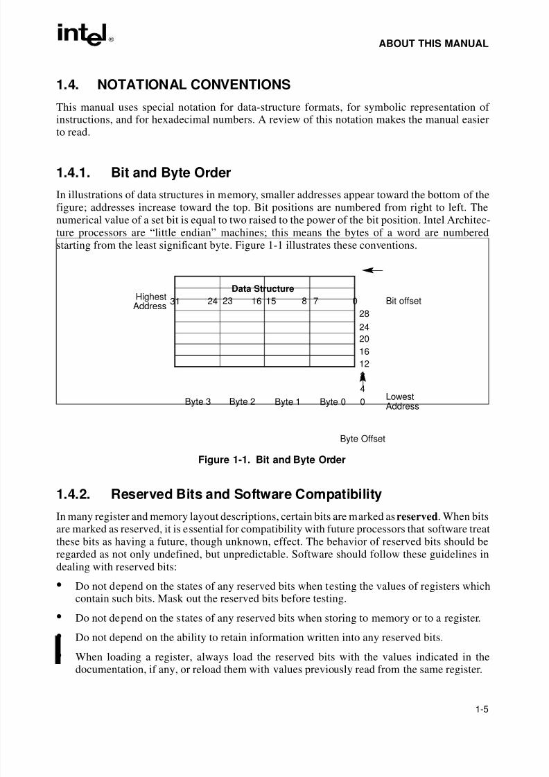
The processor uses byte addressing. This means memory is organized and accessed as asequence of bytes. Whether one or more bytes are being accessed, a byte address is used to locate
the byte or bytes memory. The range of memory that can be addressed is called an addressspace.
The processor also supports segmented addressing. This is a form of addressing where aprogram may have many independent address spaces, called segments. For example, a programcan keep its code (instructions) and stack in separate segments. Code addresses would alwaysrefer to the code space, and stack addresses would always refer to the stack space. The followingnotation is used to specify a byte address within a segment:
Segment-register:Byte-address
For example, the following segment address identifies the byte at address FF79H in the segment
pointed by the DS register:DS:FF79H
The following segment address identifies an instruction address in the code segment. The CSregister points to the code segment and the EIP register contains the address of the instruction.
CS:EIP
1.4.6. Exceptions
An exception is an event that typically occurs when an instruction causes an error. For example,an attempt to divide by zero generates an exception. However, some exceptions, such as break-points, occur under other conditions. Some types of exceptions may provide error codes. Anerror code reports additional information about the error. An example of the notation used toshow an exception and error code is shown below.
#PF(fault code)
This example refers to a page-fault exception under conditions where an error code naming atype of fault is reported. Under some conditions, exceptions which produce error codes may notbe able to report an accurate code. In this case, the error code is zero, as shown below for ageneral-protection exception.
#GP(0)
See Chapter 5, Interrupt and Exception Handling, in the Intel Architecture Software Developer’s Manual, Volume 3, for a list of exception mnemonics and their descriptions.
1.5. RELATED LITERATURE
The following books contain additional material related to Intel processors:
• Intel Pentium® Pro Processor Specification Update, Order Number 242689.
8/3/2019 Intel Architecture Software Developer's Manual, Volume 1: Basic Architecture
http://slidepdf.com/reader/full/intel-architecture-software-developers-manual-volume-1-basic-architecture 24/283
1-8
ABOUT THIS MANUAL
• Intel Pentium® Processor Specification Update, Order Number 242480.
• AP-485, Intel Processor Identification and the CPUID Instruction, Order Number 241618.
• AP-578, Software and Hardware Considerations for FPU Exception Handlers for Intel
Architecture Processors, Order Number 242415-001.
• Pentium® Pro Processor Family Developer’s Manual, Volume 1: Specifications, OrderNumber 242690-001.
• Pentium® Processor Family Developer’s Manual , Order Number 241428.
• Intel486™ Microprocessor Data Book , Order Number 240440.
• Intel486™ SX CPU/Intel487™ SX Math Coprocessor Data Book , Order Number 240950.
• Intel486™ DX2 Microprocessor Data Book , Order Number 241245.
• Intel486™ Microprocessor Product Brief Book , Order Number 240459.
• Intel386™ Processor Hardware Reference Manual , Order Number 231732.
• Intel386™ Processor System Software Writer's Guide , Order Number 231499.
• Intel386™ High-Performance 32-Bit CHMOS Microprocessor with Integrated Memory
Management , Order Number 231630.
• 376 Embedded Processor Programmer's Reference Manual, Order Number 240314.
• 80387 DX User's Manual Programmer's Reference , Order Number 231917.
•376 High-Performance 32-Bit Embedded Processor , Order Number 240182.
• Intel386™ SX Microprocessor , Order Number 240187.
• Microprocessor and Peripheral Handbook (Vol. 1), Order Number 230843.
• Intel Architecture Optimization Manual, Order Number 242816.
8/3/2019 Intel Architecture Software Developer's Manual, Volume 1: Basic Architecture
http://slidepdf.com/reader/full/intel-architecture-software-developers-manual-volume-1-basic-architecture 25/283
2Introduction to theIntel Architecture

8/3/2019 Intel Architecture Software Developer's Manual, Volume 1: Basic Architecture
http://slidepdf.com/reader/full/intel-architecture-software-developers-manual-volume-1-basic-architecture 26/283
8/3/2019 Intel Architecture Software Developer's Manual, Volume 1: Basic Architecture
http://slidepdf.com/reader/full/intel-architecture-software-developers-manual-volume-1-basic-architecture 27/283
2-1
CHAPTER 2INTRODUCTION TO THE INTEL ARCHITECTURE
A strong case can be made that the exponential growth of both the power and breadth of usageof the computer has made it the most important force that is reshaping human technology, busi-ness, and society in the second half of the twentieth century. Further, the computer promises tocontinue to dominate technological growth well into the twenty-first century, in part since otherpowerful technological forces that are just emerging are strongly dependent on the growth of computing power for their own existence and growth (such as the Internet, and genetics devel-opments like recombinant DNA research and development). The Intel Architecture is clearlytoday’s preferred computer architecture, as measured by number of computers in use and total
computing power available in the world. Thus it is hard to overestimate the importance of theIntel Architecture.
2.1. BRIEF HISTORY OF THE INTEL ARCHITECTURE
The developments leading to the Intel Architecture can be traced back through the 8085 and8080 microprocessors to the 4004 microprocessor (the first microprocessor, designed by Intel in1969). However, the first actual processor in the Intel Architecture family is the 8086, quicklyfollowed by a more cost effective version for smaller systems, the 8088. The object codeprograms created for these processors starting in 1978 will still execute on the latest members
of the Intel Architecture family.
The 8086 has 16 bit registers and a 16 bit external data bus, with 20 bit addressing giving a 1-MByte address space. The 8088 is identical except for a smaller external data bus of 8 bits. Theseprocessors introduced Intel Architecture segmentation, but only in “Real Mode”: 16-bit registerscan act as pointers to address into segments of up to 64 KBytes in size. The four segment regis-ters hold the (effectively) 20-bit base addresses of the currently active segments; up to 256KBytes can be addressed without switching between segments, and a total address range of 1MByte is available.
The Intel 80286 processor introduced the Protected Mode into the Intel Architecture. This new
mode uses the segment register contents as selectors or pointers into descriptor tables. Thedescriptors provide 24-bit base addresses, allowing a maximum physical memory size of up to16 MBytes, support for virtual memory management on a segment swapping basis, and variousprotection mechanisms. These include segment limit checking, read only and execute onlysegment options, and up to four privilege levels to protect operating system code (in severalsubdivisions, if desired) from application or user programs. Furthermore, hardware task switching and the Local Descriptor Tables allow the operating system to protect application oruser programs from each other.
The Intel386 processor introduced 32-bit registers into the architecture, for use both as operandsfor calculations and for addressing. The lower half of each 32-bit register retained the properties
of one of the 16-bit registers of the earlier two generations, to provide complete upward compat-
8/3/2019 Intel Architecture Software Developer's Manual, Volume 1: Basic Architecture
http://slidepdf.com/reader/full/intel-architecture-software-developers-manual-volume-1-basic-architecture 28/283
2-2
INTRODUCTION TO THE INTEL ARCHITECTURE
ibility. A new virtual-8086 mode was provided to yield greater efficiency when executingprograms created for the 8086 and 8088 processors on the new 32-bit machine. The 32-bitaddressing was supported with an external 32-bit address bus, giving a 4-GByte address space,and also allowed each segment to be as large as 4 GBytes. The original instructions were
enhanced with new 32-bit operand and addressing forms, and completely new instructions wereprovided, including those for bit manipulation. The Intel386 processor also introduced paginginto the Intel Architecture, with the fixed 4-KByte page size providing a method for virtualmemory management that was significantly superior compared to using segments for thepurpose (it was much more efficient for operating systems, and completely transparent to theapplications without significant sacrifice of execution speed). Furthermore, the ability to definesegments as large as the 4 GBytes physical address space, together with paging, allowed thecreation of protected “flat model”1 addressing systems in the architecture, including completeimplementations of the widely used main-frame operating system UNIX.
The Intel Architecture has been and is committed to the task of maintaining backward compat-
ibility at the object code level to preserve our customers’ very large investment in software, butat the same time, in each generation of the architecture the latest most effective microprocessorarchitecture and silicon fabrication technologies have been used to produce the fastest, mostpowerful processors possible. Intel has worked over the generations to adapt and incorporateincreasingly sophisticated techniques from main-frame architecture into microprocessor archi-tecture. Various forms of parallel processing have been the most performance enhancing of thesetechniques, and the Intel386 processor was the first Intel Architecture processor to include anumber of parallel stages: six. These are the Bus Interface Unit (accesses memory and I/O forthe other units), the Code Prefetch Unit (receives object code from the Bus Unit and puts it intoa 16 byte queue), the Instruction Decode Unit (decodes object code from the Prefetch unit intomicrocode), the Execution Unit (executes the microcode instructions), the Segment Unit (trans-lates logical addresses to linear addresses and does protection checks), and the Paging Unit(translates linear addresses to physical addresses, does page based protection checks, andcontains a cache with information for up to 32 most recently accessed pages).
The Intel486 processor added more parallel execution capability by (basically) expanding theIntel386 processor’s Instruction Decode and Execution Units into five pipelined stages, whereeach stage (when needed) operates in parallel with the others on up to five instructions indifferent stages of execution. Each stage can do its work on one instruction in one clock, and sothe Intel486 processor can execute as rapidly as one instruction per CPU clock. An 8-KByte onchip L1 cache was added to the Intel486 processor to greatly increase the percent of instructionsthat could execute at the scalar rate of one per clock: memory access instructions were nowincluded if the operand was in the L1 cache. The Intel486 processor also for the first time inte-grated the Floating-Point math Unit onto the same chip as the CPU (see section 2.3 below) andadded new pins, bits and instructions to support more complex and powerful systems (L2 cachesupport and multiprocessor support).
Late in the Intel486 processor generation, Intel incorporated features designed to support energysavings and other system management capabilities into the Intel Architecture mainstream withthe Intel486 SL Enhanced processors. These features were developed in the Intel386 SL andIntel486 SL processors, which were specialized for the rapidly growing battery operated note-
1. Requires ony one 32-bit address component to access anywhere in the address space.
8/3/2019 Intel Architecture Software Developer's Manual, Volume 1: Basic Architecture
http://slidepdf.com/reader/full/intel-architecture-software-developers-manual-volume-1-basic-architecture 29/283
2-3
INTRODUCTION TO THE INTEL ARCHITECTURE
book PC market. The features include the new System Management Mode, triggered by its owndedicated interrupt pin, which allows complex system management features (such as powermanagement of various subsystems within the PC), to be added to a system transparently to themain operating system and all applications. The Stop Clock and Auto Halt Powerdown features
allow the CPU itself to execute at a reduced clock rate to save power, or to be shut down (withstate preserved) to save even more power.
The Intel Pentium processor added a second execution pipeline to achieve superscalar perfor-mance (two pipelines, known as u and v, together can execute two instructions per clock). Theon-chip L1 cache has also been doubled, with 8 KBytes devoted to code, and another 8 KBytesto data. The data cache uses the MESI protocol to support the more efficient write-back mode,as well as the write-through mode that is used by the Intel486 processor. Branch prediction withan on-chip branch table has been added to increase performance in looping constructs. Exten-sions have been added to make the virtual-8086 mode more efficient, and to allow for 4-MByteas well as 4-KByte pages. The main registers are still 32 bits, but internal data paths of 128 and
256-bits have been added to speed internal data transfers, and the burstable external data bus hasbeen increased to 64 bits. The Advanced Programmable Interrupt Controller (APIC) has beenadded to support systems with multiple Pentium processors, and new pins and a special mode(dual processing) has been designed in to support glueless two processor systems.
The Intel Pentium Pro processor is the latest and most powerful member of the Intel Architec-ture. It has three-way superscalar architecture, which means that it can execute three instructionsper CPU clock. It does this by incorporating even more parallelism than the Pentium processor.The Pentium Pro processor provides Dynamic Execution (micro-data flow analysis, out-of-order execution, superior branch prediction, and speculative execution) in a superscalar imple-mentation. Three instruction decode units work in parallel to decode object code into smaller
operations called “micro-ops.” These go into an instruction pool, and (when interdependenciesdon’t prevent) can be executed out of order by the five parallel execution units (two integer, twoFPU and one memory interface unit). The Retirement Unit retires completed micro-ops in theiroriginal program order, taking account of any branches. The power of the Pentium Pro processoris further enhanced by its caches: it has the same two on-chip 8-KByte L1 caches as does thePentium processor, and also has a 256-KByte L2 cache that’s in the same package as, and closelycoupled to, the CPU, using a dedicated 64-bit (“backside”) full clock speed bus. The L1 cacheis dual ported, the L2 cache supports up to 4 concurrent accesses, and the 64-bit external databus is transaction-oriented, meaning that each access is handled as a separate request andresponse, with numerous requests allowed while awaiting a response. These parallel features fordata access work with the parallel execution capabilities to provide a “non-blocking” architec-ture in which the processor is more fully utilized and performance is enhanced. The Pentium Proprocessor also has an expanded 36-bit address bus, giving a maximum physical address space of 64 GBytes.
Since the Pentium Pro processor is currently the most advanced of the Intel Architecture family,a more detailed description of its architecture is provided in Sections 2.4. and 2.5. More detailedhardware and architectural information on each of the generations of the Intel Architecturefamily is available in the separate data books for the processor generations (see Section 1.5.,
Related Literature).
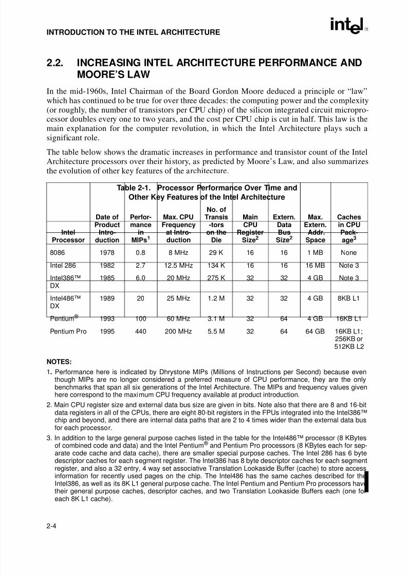
8/3/2019 Intel Architecture Software Developer's Manual, Volume 1: Basic Architecture
http://slidepdf.com/reader/full/intel-architecture-software-developers-manual-volume-1-basic-architecture 30/283
2-4
INTRODUCTION TO THE INTEL ARCHITECTURE
2.2. INCREASING INTEL ARCHITECTURE PERFORMANCE ANDMOORE’S LAW
In the mid-1960s, Intel Chairman of the Board Gordon Moore deduced a principle or “law”
which has continued to be true for over three decades: the computing power and the complexity(or roughly, the number of transistors per CPU chip) of the silicon integrated circuit micropro-cessor doubles every one to two years, and the cost per CPU chip is cut in half. This law is themain explanation for the computer revolution, in which the Intel Architecture plays such asignificant role.
The table below shows the dramatic increases in performance and transistor count of the IntelArchitecture processors over their history, as predicted by Moore’s Law, and also summarizesthe evolution of other key features of the architecture.
NOTES:
1. Performance here is indicated by Dhrystone MIPs (Millions of Instructions per Second) because eventhough MIPs are no longer considered a preferred measure of CPU performance, they are the onlybenchmarks that span all six generations of the Intel Architecture. The MIPs and frequency values given
here correspond to the maximum CPU frequency available at product introduction.2. Main CPU register size and external data bus size are given in bits. Note also that there are 8 and 16-bit
data registers in all of the CPUs, there are eight 80-bit registers in the FPUs integrated into the Intel386™chip and beyond, and there are internal data paths that are 2 to 4 times wider than the external data busfor each processor.
3. In addition to the large general purpose caches listed in the table for the Intel486™ processor (8 KBytesof combined code and data) and the Intel Pentium ® and Pentium Pro processors (8 KBytes each for sep-arate code cache and data cache), there are smaller special purpose caches. The Intel 286 has 6 bytedescriptor caches for each segment register. The Intel386 has 8 byte descriptor caches for each segmentregister, and also a 32 entry, 4 way set associative Translation Lookaside Buffer (cache) to store accessinformation for recently used pages on the chip. The Intel486 has the same caches described for theIntel386, as well as its 8K L1 general purpose cache. The Intel Pentium and Pentium Pro processors have
their general purpose caches, descriptor caches, and two Translation Lookaside Buffers each (one foreach 8K L1 cache).
Table 2-1. Processor Performance Over Time and
Other Key Features of the Intel Architecture
IntelProcessor
Date ofProduct
Intro-duction
Perfor-mance
inMIPs1
Max. CPUFrequency
at Intro-duction
No. ofTransis
-torson the
Die
MainCPU
RegisterSize2
Extern.DataBus
Size2
Max.Extern.
Addr.Space
Cachesin CPUPack-age3
8086 1978 0.8 8 MHz 29 K 16 16 1 MB None
Intel 286 1982 2.7 12.5 MHz 134 K 16 16 16 MB Note 3
Intel386™DX
1985 6.0 20 MHz 275 K 32 32 4 GB Note 3
Intel486™DX
1989 20 25 MHz 1.2 M 32 32 4 GB 8KB L1
Pentium ® 1993 100 60 MHz 3.1 M 32 64 4 GB 16KB L1
Pentium Pro 1995 440 200 MHz 5.5 M 32 64 64 GB 16KB L1;256KB or512KB L2
8/3/2019 Intel Architecture Software Developer's Manual, Volume 1: Basic Architecture
http://slidepdf.com/reader/full/intel-architecture-software-developers-manual-volume-1-basic-architecture 31/283
2-5
INTRODUCTION TO THE INTEL ARCHITECTURE
2.3. BRIEF HISTORY OF THE INTEL ARCHITECTURE FLOATING-POINT UNIT
The Intel Architecture Floating-Point Units (FPUs) before the Intel486 lack the added efficiency
of integration into the CPU, but have provided the option of greatly enhanced floating-pointperformance since the beginning of the family. (Since the earlier FPUs were on separate chips,they were often referred to as numeric processor extensions (NPXs) or math coprocessors(MCPs).) With each succeeding generation, Intel has made significant increases in the powerand flexibility of the FPU, and yet has maintained complete upward compatibility. The PentiumPro Processor offers compatibility with object code for 8087, Intel 287, Intel 387 DX, Intel 387SX, and Intel 487 DX math coprocessors and the Intel486 DX and Pentium processors.
The 8087 numeric processor extension (NPX) was designed for use in 8086-family systems. The8086 was the first microprocessor family to partition the processing unit to permit high-perfor-mance numeric capabilities. The 8087 NPX for this processor family implemented a complete
numeric processing environment in compliance with an early proposal for IEEE Standard 754for Binary Floating-Point Arithmetic.
With the Intel 287 coprocessor NPX, high-speed numeric computations were extended to 80286high-performance multitasking and multi-user systems. Multiple tasks using the numericprocessor extension were afforded the full protection of the 80286 memory management andprotection features.
The Intel 387 DX and SX math coprocessors are Intel’s third generation numeric processors.They implement the final IEEE Std 754, adding new trigonometric instructions, and using a newdesign and CHMOS-III process to allow higher clock rates and require fewer clocks per instruc-
tion. Together, the Intel 387 math coprocessor with additional instructions and the improvedstandard brought even more convenience and reliability to numeric programming and made thisconvenience and reliability available to applications that need the high-speed and large memorycapacity of the 32-bit environment of the Intel386 microprocessor.
The Intel486 processor FPU is an on-chip equivalent of the Intel 387 DX math coprocessorconforming to both IEEE Std 754 and the more recent, generalized IEEE Std 854. Having theFPU on chip results in a considerable performance improvement in numeric-intensive computa-tion.
The Pentium processor FPU has been completely redesigned over the Intel486 processor FPUwhile maintaining conformance to both the IEEE Std 754 and 854. Faster algorithms provide at
least three times the performance over the Intel486 processor FPU for common operationsincluding ADD, MUL, and LOAD. Many applications can achieve five times the performanceof the Intel486 processor FPU or more with instruction scheduling and pipelined execution.
2.4. INTRODUCTION TO THE PENTIUM ® PRO PROCESSOR’SADVANCED MICROARCHITECTURE
The Pentium Pro processor (introduced by Intel in 1995) represents the most recent implemen-tation of the Intel Architecture. Like its predecessor, the Pentium processor (introduced by Intel
in 1993), the Pentium Pro processor, with its advanced superscalar microarchitecture, sets animpressive performance standard. In designing the Pentium Pro processor, one of the primary
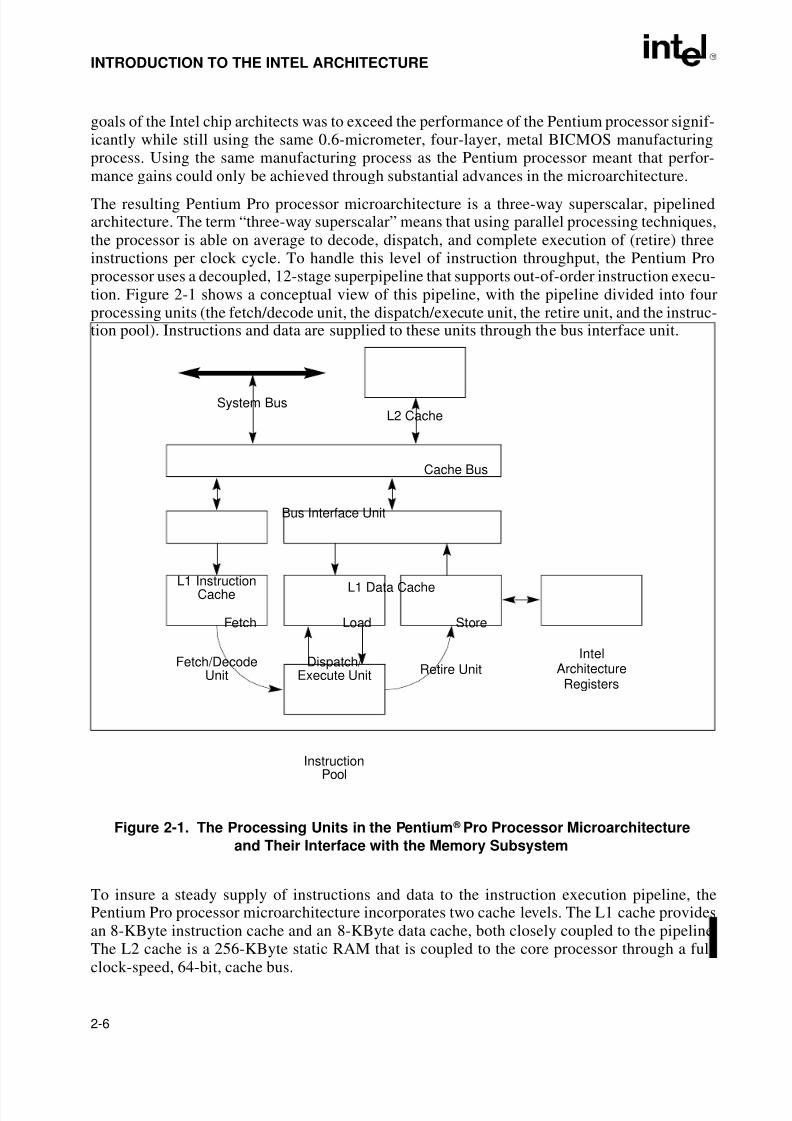
8/3/2019 Intel Architecture Software Developer's Manual, Volume 1: Basic Architecture
http://slidepdf.com/reader/full/intel-architecture-software-developers-manual-volume-1-basic-architecture 32/283
2-6
INTRODUCTION TO THE INTEL ARCHITECTURE
goals of the Intel chip architects was to exceed the performance of the Pentium processor signif-icantly while still using the same 0.6-micrometer, four-layer, metal BICMOS manufacturingprocess. Using the same manufacturing process as the Pentium processor meant that perfor-mance gains could only be achieved through substantial advances in the microarchitecture.
The resulting Pentium Pro processor microarchitecture is a three-way superscalar, pipelinedarchitecture. The term “three-way superscalar” means that using parallel processing techniques,the processor is able on average to decode, dispatch, and complete execution of (retire) threeinstructions per clock cycle. To handle this level of instruction throughput, the Pentium Proprocessor uses a decoupled, 12-stage superpipeline that supports out-of-order instruction execu-tion. Figure 2-1 shows a conceptual view of this pipeline, with the pipeline divided into fourprocessing units (the fetch/decode unit, the dispatch/execute unit, the retire unit, and the instruc-tion pool). Instructions and data are supplied to these units through the bus interface unit.
To insure a steady supply of instructions and data to the instruction execution pipeline, thePentium Pro processor microarchitecture incorporates two cache levels. The L1 cache providesan 8-KByte instruction cache and an 8-KByte data cache, both closely coupled to the pipeline.The L2 cache is a 256-KByte static RAM that is coupled to the core processor through a full
clock-speed, 64-bit, cache bus.
Figure 2-1. The Processing Units in the Pentium ® Pro Processor Microarchitecture
and Their Interface with the Memory Subsystem
Architecture
Cache Bus
Fetch/DecodeUnit
Dispatch/ Execute Unit Retire Unit
Registers
Intel
InstructionPool
L1 InstructionCache
L1 Data Cache
Fetch Load Store
Bus Interface Unit
L2 CacheSystem Bus
8/3/2019 Intel Architecture Software Developer's Manual, Volume 1: Basic Architecture
http://slidepdf.com/reader/full/intel-architecture-software-developers-manual-volume-1-basic-architecture 33/283
2-7
INTRODUCTION TO THE INTEL ARCHITECTURE
The centerpiece of the Pentium Pro processor microarchitecture is an innovative out-of-orderexecution mechanism called “dynamic execution.” Dynamic execution incorporates three data-processing concepts:
• Deep branch prediction.• Dynamic data flow analysis.
• Speculative execution.
Branch prediction is a concept found in most mainframe and high-speed microprocessor archi-tectures. It allows the processor to decode instructions beyond branches to keep the instructionpipeline full. In the Pentium Pro processor, the instruction fetch/decode unit uses a highly opti-mized branch prediction algorithm to predict the direction of the instruction stream throughmultiple levels of branches, procedure calls, and returns.
Dynamic data flow analysis involves real-time analysis of the flow of data through the processor
to determine data and register dependencies and to detect opportunities for out-of-order instruc-tion execution. The Pentium Pro processor dispatch/execute unit can simultaneously monitormany instructions and execute these instructions in the order that optimizes the use of theprocessor’s multiple execution units, while maintaining the integrity of the data being operatedon. This out-of-order execution keeps the execution units busy even when cache misses and datadependencies among instructions occur.
Speculative execution refers to the processor’s ability to execute instructions ahead of theprogram counter but ultimately to commit the results in the order of the original instructionstream. To make speculative execution possible, the Pentium Pro processor microarchitecturedecouples the dispatching and executing of instructions from the commitment of results. The
processor’s dispatch/execute unit uses data-flow analysis to execute all available instructions inthe instruction pool and store the results in temporary registers. The retirement unit then linearlysearches the instruction pool for completed instructions that no longer have data dependencieswith other instructions or unresolved branch predictions. When completed instructions arefound, the retirement unit commits the results of these instructions to memory and/or the IntelArchitecture registers (the processor’s eight general-purpose registers and eight floating-pointunit data registers) in the order they were originally issued and retires the instructions from theinstruction pool.
Through deep branch prediction, dynamic data-flow analysis, and speculative execution,dynamic execution removes the constraint of linear instruction sequencing between the tradi-
tional fetch and execute phases of instruction execution. It allows instructions to be decodeddeep into multi-level branches to keep the instruction pipeline full. It promotes out-of-orderinstruction execution to keep the processor’s six instruction execution units running at fullcapacity. And finally it commits the results of executed instructions in original program order tomaintain data integrity and program coherency.
The following section describes the Pentium Pro processor microarchitecture in greater detail.
8/3/2019 Intel Architecture Software Developer's Manual, Volume 1: Basic Architecture
http://slidepdf.com/reader/full/intel-architecture-software-developers-manual-volume-1-basic-architecture 34/283
2-8
INTRODUCTION TO THE INTEL ARCHITECTURE
2.5. DETAILED DESCRIPTION OF THE PENTIUM ® PROPROCESSOR MICROARCHITECTURE
Figure 2-2 shows a functional block diagram of the Pentium Pro processor microarchitecture. In
this diagram, the following blocks make up the four processing units and the memory subsystemshown in Figure 2-1:
• Memory subsystem—System bus, L2 cache, bus interface unit, instruction cache (L1), datacache unit (L1), memory interface unit, and memory reorder buffer.
• Fetch/decode unit—Instruction fetch unit, branch target buffer, instruction decoder,microcode sequencer, and register alias table.
• Instruction pool—Reorder buffer
• Dispatch/execute unit—Reservation station, two integer units, two floating-point units, and
two address generation units.• Retire unit—Retire unit and retirement register file.
2.5.1. Memory Subsystem
The memory subsystem for the Pentium Pro processor consists of main system memory, theprimary cache (L1), and the secondary cache (L2). The bus interface unit accesses systemmemory through the external system bus. This 64-bit bus is a transaction-oriented bus, meaningthat each bus access is handled as separate request and response operations. While the bus inter-
face unit is waiting for a response to one bus request, it can issue numerous additional requests.The bus interface unit accesses the close-coupled L2 cache through a 64-bit cache bus. This busis also transactional oriented, supporting up to four concurrent cache accesses, and operates atthe full clock speed of the processor.
Access to the L1 caches is through internal buses, also at full clock speed. The 8-KByte L1instruction cache is four-way set associative; the 8-KByte L1 data cache is dual-ported and two-way set associative, supporting one load and one store operation per cycle.
Coherency between the caches and system memory are maintained using the MESI (modified,exclusive, shared, invalid) cache protocol. This protocol fosters cache coherency in single- and
multiple-processor systems. It is also able to detect coherency problems created by self-modi-fying code.
Memory requests from the processor’s execution units go through the memory interface unit andthe memory order buffer. These units have been designed to support a smooth flow of memoryaccess requests through the cache and system memory hierarchy to prevent memory accessblocking. The L1 data cache automatically forwards a cache miss on to the L2 cache, and then,if necessary, the bus interface unit forwards an L2 cache miss to system memory.
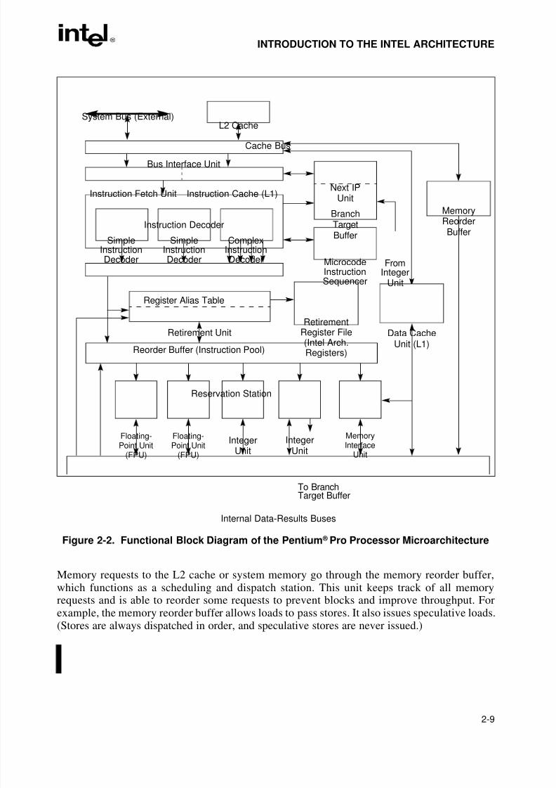
8/3/2019 Intel Architecture Software Developer's Manual, Volume 1: Basic Architecture
http://slidepdf.com/reader/full/intel-architecture-software-developers-manual-volume-1-basic-architecture 35/283
2-9
INTRODUCTION TO THE INTEL ARCHITECTURE
Memory requests to the L2 cache or system memory go through the memory reorder buffer,which functions as a scheduling and dispatch station. This unit keeps track of all memoryrequests and is able to reorder some requests to prevent blocks and improve throughput. Forexample, the memory reorder buffer allows loads to pass stores. It also issues speculative loads.(Stores are always dispatched in order, and speculative stores are never issued.)
Figure 2-2. Functional Block Diagram of the Pentium ® Pro Processor Microarchitecture
Branch
Next IP
Microcode
InstructionSequencer
SimpleInstructionDecoder
Register Alias Table
Instruction Decoder
Instruction Cache (L1)Instruction Fetch Unit
Bus Interface Unit
Reorder Buffer (Instruction Pool)
Internal Data-Results Buses
IntegerUnit
IntegerUnit
Floating-
(FPU)Point Unit
MemoryInterface
Unit
MemoryReorderBuffer
Data CacheUnit (L1)
L2 CacheSystem Bus (External)
Retirement UnitRetirement
Register File(Intel Arch.Registers)
Cache Bus
TargetBuffer
Unit
To BranchTarget Buffer
FromInteger
Unit
Floating-
(FPU)Point Unit
SimpleInstructionDecoder
ComplexInstructionDecoder
Reservation Station
8/3/2019 Intel Architecture Software Developer's Manual, Volume 1: Basic Architecture
http://slidepdf.com/reader/full/intel-architecture-software-developers-manual-volume-1-basic-architecture 36/283
8/3/2019 Intel Architecture Software Developer's Manual, Volume 1: Basic Architecture
http://slidepdf.com/reader/full/intel-architecture-software-developers-manual-volume-1-basic-architecture 37/283
2-11
INTRODUCTION TO THE INTEL ARCHITECTURE
The reorder buffer is an array of content-addressable memory, arranged into 40 micro-op regis-ters. It contains micro-ops that are waiting to be executed, as well as those that have already beenexecuted but not yet committed to machine state. The dispatch/execute unit can execute instruc-tions from the reorder buffer in any order.
2.5.4. Dispatch/Execute Unit
The dispatch/execute unit is an out-of-order unit that schedules and executes the micro-opsstored in the reorder buffer according to data dependencies and resource availability and tempo-rarily stores the results of these speculative executions.
The scheduling and dispatching of micro-ops from the reorder buffer is handled by the reserva-tion station. It continuously scans the reorder buffer for micro-ops that are ready to be executed(that is, all the source operands are available) and dispatches them to the available execution
units. The results of a micro-op execution are returned to the reorder buffer and stored along withthe micro-op until it is retired. This scheduling and dispatching process supports classic out-of-order execution, where micro-ops are dispatched to the execution units strictly according todata-flow constraints and execution resource availability, without regard to the original orderingof the instructions. When two or more micro-ops of the same type (for example, integer opera-tions) are available at the same time, they are executed in a pseudo FIFO order in the reorderbuffer.
Execution of micro-ops is handled by two integer units, two floating-point units, and onememory-interface unit, allowing up to five micro-ops can be scheduled per clock.
The two integer units can handle two integer micro-ops in parallel. One of the integer units isdesigned to handle branch micro-ops. This unit has the ability to detect branch mispredictionsand signal the branch target buffer to restart the pipeline. This operation is handled as follows.The instruction decoder tags each branch micro-op with both branch destination addresses (thepredicted destination and the fall-through destination). When the integer unit executes thebranch micro-op, it is able to determine whether the predicted or the fall-through destination wastaken. If the predicted branch is taken, then speculatively executed micro-ops are marked usableand execution continues along the predicted instruction path. If the predicted branch was nottaken, a jump execution unit in the integer unit changes the status of all of the micro-opsfollowing the branch to remove them from the instruction pool. It then provides the properbranch destination to the branch target buffer, which in turn restarts the pipeline from the new
target address.
The memory interface unit handles load and store micro-ops. A load access only needs to specifythe memory address, so it can be encoded in one micro-op. A store access needs to specify bothan address and the data to be written, so it is encoded in two micro-ops. The part of the memoryinterface unit that handles stores has two ports allowing it to process the address and the datamicro-op in parallel. The memory interface unit can thus execute both a load and a store inparallel in one clock cycle.
The floating-point execution units are similar to those found in the Pentium processor. Severalnew floating-point instructions have been added to the Pentium Pro processor to streamlineconditional branches and moves.
8/3/2019 Intel Architecture Software Developer's Manual, Volume 1: Basic Architecture
http://slidepdf.com/reader/full/intel-architecture-software-developers-manual-volume-1-basic-architecture 38/283
2-12
INTRODUCTION TO THE INTEL ARCHITECTURE
2.5.5. Retirement Unit
The retirement unit commits the results of speculatively executed micro-ops to permanentmachine state and removes the micro-ops from the reorder buffer. Like the reservation station,
the retirement unit continuously checks the status of micro-ops in the reorder buffer, looking forones that have been executed and no longer have any dependencies with other micro-ops in theinstruction pool. It then retires completed micro-ops in their original program order, taking intoaccounts interrupts, exceptions, breakpoints, and branch mispredictions.
The retirement unit can retire three micro-ops per clock. In retiring a micro-op, it writes theresults to the retirement register file and/or memory. The retirement register file contains theIntel Architecture registers (eight general-purpose registers and eight floating-point data regis-ters). After the results have been committed to machine state, the micro-op is removed from thereorder buffer.
8/3/2019 Intel Architecture Software Developer's Manual, Volume 1: Basic Architecture
http://slidepdf.com/reader/full/intel-architecture-software-developers-manual-volume-1-basic-architecture 39/283
3Basic ExecutionEnvironment

8/3/2019 Intel Architecture Software Developer's Manual, Volume 1: Basic Architecture
http://slidepdf.com/reader/full/intel-architecture-software-developers-manual-volume-1-basic-architecture 40/283
8/3/2019 Intel Architecture Software Developer's Manual, Volume 1: Basic Architecture
http://slidepdf.com/reader/full/intel-architecture-software-developers-manual-volume-1-basic-architecture 41/283
3-1
CHAPTER 3BASIC EXECUTION ENVIRONMENT
This chapter describes the basic execution environment of an Intel Architecture processor asseen by assembly-language programmers. It describes how the processor executes instructionsand how it stores and manipulates data. The parts of the execution environment described hereinclude memory (the address space), the general-purpose data registers, the segment registers,the EFLAGS register, and the instruction pointer register.
The execution environment for the floating-point unit (FPU) is described in Chapter 7, Floating-Point Unit .
3.1. MODES OF OPERATION
The Intel Architecture supports three operating modes: protected mode, real-address mode, andsystem management mode. The operating mode determines which instructions and architecturalfeatures are accessible:
• Protected mode. The native state of the processor. In this mode all instructions and archi-tectural features are available, providing the highest performance and capability. This is therecommended mode for all new applications and operating systems.
Among the capabilities of protected mode is the ability to directly execute “real-addressmode” 8086 software in a protected, multi-tasking environment. This feature is called
virtual-8086 mode, although it is not actually a processor mode. Virtual-8086 mode isactually a protected mode attribute that can be enabled for any task.
• Real-address mode. Provides the programming environment of the Intel 8086 processorwith a few extensions (such as the ability to switch to protected or system managementmode). The processor is placed in real-address mode following power-up or a reset.
• System management mode. A standard architectural feature unique to all Intelprocessors, beginning with the Intel386 SL processor. This mode provides an operatingsystem or executive with a transparent mechanism for implementing platform-specificfunctions such as power management and system security. The processor enters SMMwhen the external SMM interrupt pin (SMI#) is activated or an SMI is received from theadvanced programmable interrupt controller (APIC). In SMM, the processor switches to aseparate address space while saving the entire context of the currently running program ortask. SMM-specific code may then be executed transparently. Upon returning from SMM,the processor is placed back into its state prior to the system management interrupt.
The basic execution environment is the same for each of these operating modes, as is describedin the remaining sections of this chapter.

8/3/2019 Intel Architecture Software Developer's Manual, Volume 1: Basic Architecture
http://slidepdf.com/reader/full/intel-architecture-software-developers-manual-volume-1-basic-architecture 42/283
3-2
BASIC EXECUTION ENVIRONMENT
3.2. OVERVIEW OF THE BASIC EXECUTION ENVIRONMENT
Any program or task running on an Intel Architecture processor is given a set of resources forexecuting instructions and for storing code, data, and state information. These resources (shown
in Figure 3-1) include an address space of up to 232 bytes, a set of general data registers, a set of segment registers, and a set of status and control registers. When a program calls a procedure, aprocedure stack is added to the execution environment. (Procedure calls and the procedure stack implementation are described in Chapter 4, Procedure Calls, Interrupts, and Exceptions.)
3.3. MEMORY ORGANIZATION
The memory that the processor addresses on its bus is called physical memory. Physicalmemory is organized as a sequence of 8-bit bytes. Each byte is assigned a unique address, calleda physical address. The physical address space ranges from zero to a maximum of 232 – 1(4 gigabytes).
Virtually any operating system or executive designed to work with an Intel Architecture
processor will use the processor’s memory management facilities to access memory. These facil-ities provide features such as segmentation and paging, which allow memory to be managed effi-ciently and reliably. Memory management is described in detail in Chapter 3, Protected-Mode
Memory Management , of the Intel Architecture Software Developer’s Manual, Volume 3. Thefollowing paragraphs describe the basic methods of addressing memory when memory manage-ment is used.
When employing the processor’s memory management facilities, programs do not directlyaddress physical memory. Instead, they access memory using any of three memory models: flat,segmented, or real-address mode.
Figure 3-1. Pentium ® Pro Processor Basic Execution Environment
0
232 −1
Eight 32-bit
32-bits
32-bits
General-PurposeRegisters
Segment Registers
EFLAGS Register
EIP (InstructionPointer Register)
Space*Address
*The address space can be flat or segmented.
Six 16-bitRegisters
Registers
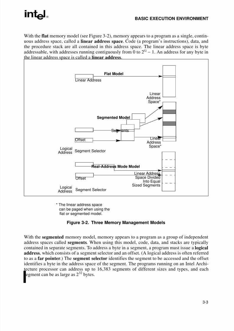
8/3/2019 Intel Architecture Software Developer's Manual, Volume 1: Basic Architecture
http://slidepdf.com/reader/full/intel-architecture-software-developers-manual-volume-1-basic-architecture 43/283
3-3
BASIC EXECUTION ENVIRONMENT
With the flat memory model (see Figure 3-2), memory appears to a program as a single, contin-uous address space, called a linear address space. Code (a program’s instructions), data, andthe procedure stack are all contained in this address space. The linear address space is byteaddressable, with addresses running contiguously from 0 to 232 − 1. An address for any byte in
the linear address space is called a linear address.
With the segmented memory model, memory appears to a program as a group of independentaddress spaces called segments. When using this model, code, data, and stacks are typicallycontained in separate segments. To address a byte in a segment, a program must issue a logicaladdress, which consists of a segment selector and an offset. (A logical address is often referredto as a far pointer.) The segment selector identifies the segment to be accessed and the offsetidentifies a byte in the address space of the segment. The programs running on an Intel Archi-tecture processor can address up to 16,383 segments of different sizes and types, and eachsegment can be as large as 232 bytes.
Figure 3-2. Three Memory Management Models
Linear Address
Flat Model
LinearAddressSpace*
Segment Selector
Offset
Segment Selector
Segmented Model
Real-Address Mode Model
Linear Address
Logical
Offset
Space DividedInto Equal
Sized Segments
Address
LogicalAddress
LinearAddress
Space*
Segments
* The linear address spacecan be paged when using theflat or segmented model.
8/3/2019 Intel Architecture Software Developer's Manual, Volume 1: Basic Architecture
http://slidepdf.com/reader/full/intel-architecture-software-developers-manual-volume-1-basic-architecture 44/283
3-4
BASIC EXECUTION ENVIRONMENT
Internally, all the segments that are defined for a system are mapped into the processor’s linearaddress space. So, the processor translates each logical address into a linear address to access amemory location. This translation is transparent to the application program.
The primary reason for using segmented memory is to increase the reliability of programs andsystems. For example, placing a program’s stack in a separate segment prevents the stack fromgrowing into the code or data space and overwriting instructions or data, respectively. Andplacing the operating system’s or executive’s code, data, and stack in separate segments protectsthem from the application program and vice versa.
With either the flat or segmented model, the Intel Architecture provides facilities for dividingthe linear address space into pages and mapping the pages into virtual memory. If an operatingsystem/executive uses the Intel Architecture’s paging mechanism, the existence of the pages istransparent to an application program.
The real-address mode model uses the memory model for the Intel 8086 processor, the first
Intel Architecture processor. It was provided in all the subsequent Intel Architecture processorsfor compatibility with existing programs written to run on the Intel 8086 processor. The real-address mode uses a specific implementation of segmented memory in which the linear addressspace for the program and the operating system/executive consists of an array of segments of upto 64K bytes in size each. The maximum size of the linear address space in real-address modeis 220 bytes. (See Chapter 15, 8086 Emulation, in the Intel Architecture Software Developer’s
Manual, Volume 3, for more information on this memory model.)
3.4. MODES OF OPERATION
When writing code for the Pentium Pro processor, a programmer needs to know the operatingmode the processor is going to be in when executing the code and the memory model being used.The relationship between operating modes and memory models is as follows:
• Protected mode. When in protected mode, the processor can use any of the memorymodels described in this section. (The real-addressing mode memory model is ordinarilyused only when the processor is in the virtual-8086 mode.) The memory model useddepends on the design of the operating system or executive. When multitasking is imple-mented, individual tasks can use different memory models.
• Real-address mode. When in real-address mode, the processor only supports the real-
address mode memory model.
• System management mode. When in SMM, the processor switches to a separate addressspace, called the system management RAM (SMRAM). The memory model used toaddress bytes in this address space is similar to the real-address mode model. (See Chapter11, in the Intel Architecture Software Developer’s Manual, Volume 3, for more informationon the memory model used in SMM.)
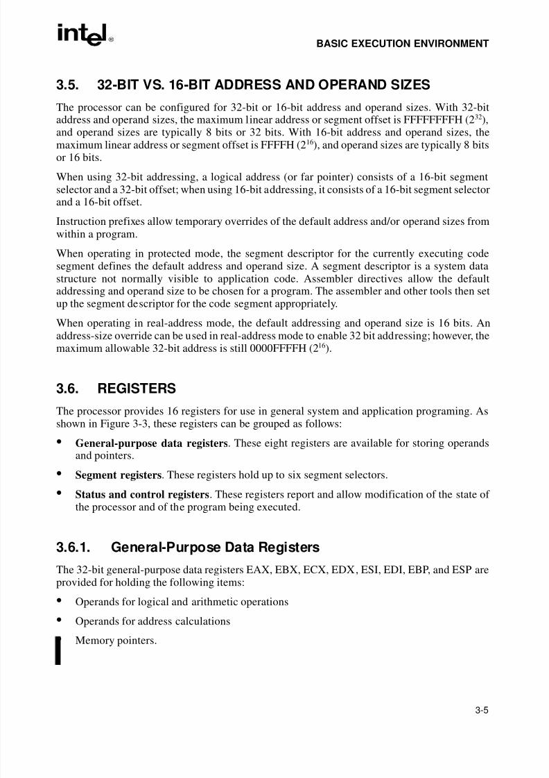
8/3/2019 Intel Architecture Software Developer's Manual, Volume 1: Basic Architecture
http://slidepdf.com/reader/full/intel-architecture-software-developers-manual-volume-1-basic-architecture 45/283
3-5
BASIC EXECUTION ENVIRONMENT
3.5. 32-BIT VS. 16-BIT ADDRESS AND OPERAND SIZES
The processor can be configured for 32-bit or 16-bit address and operand sizes. With 32-bitaddress and operand sizes, the maximum linear address or segment offset is FFFFFFFFH (232),
and operand sizes are typically 8 bits or 32 bits. With 16-bit address and operand sizes, themaximum linear address or segment offset is FFFFH (216), and operand sizes are typically 8 bitsor 16 bits.
When using 32-bit addressing, a logical address (or far pointer) consists of a 16-bit segmentselector and a 32-bit offset; when using 16-bit addressing, it consists of a 16-bit segment selectorand a 16-bit offset.
Instruction prefixes allow temporary overrides of the default address and/or operand sizes fromwithin a program.
When operating in protected mode, the segment descriptor for the currently executing code
segment defines the default address and operand size. A segment descriptor is a system datastructure not normally visible to application code. Assembler directives allow the defaultaddressing and operand size to be chosen for a program. The assembler and other tools then setup the segment descriptor for the code segment appropriately.
When operating in real-address mode, the default addressing and operand size is 16 bits. Anaddress-size override can be used in real-address mode to enable 32 bit addressing; however, themaximum allowable 32-bit address is still 0000FFFFH (216).
3.6. REGISTERS
The processor provides 16 registers for use in general system and application programing. Asshown in Figure 3-3, these registers can be grouped as follows:
• General-purpose data registers. These eight registers are available for storing operandsand pointers.
• Segment registers. These registers hold up to six segment selectors.
• Status and control registers. These registers report and allow modification of the state of the processor and of the program being executed.
3.6.1. General-Purpose Data Registers
The 32-bit general-purpose data registers EAX, EBX, ECX, EDX, ESI, EDI, EBP, and ESP areprovided for holding the following items:
• Operands for logical and arithmetic operations
• Operands for address calculations
• Memory pointers.
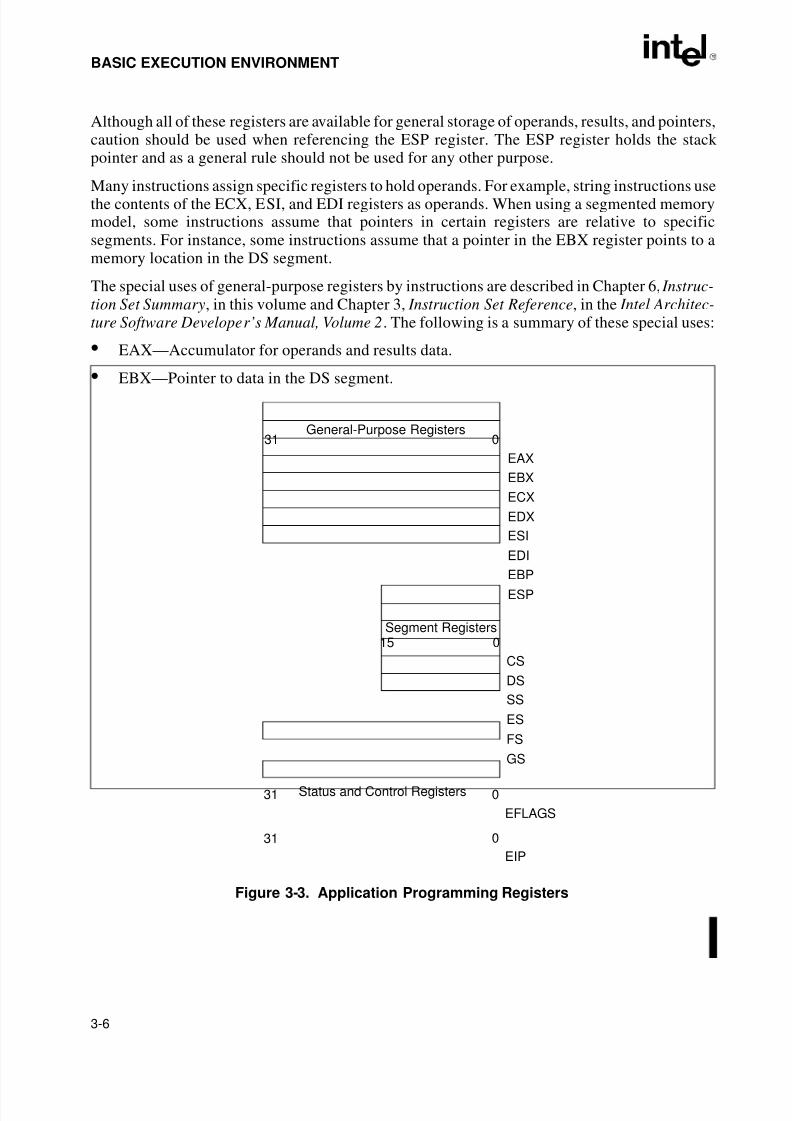
8/3/2019 Intel Architecture Software Developer's Manual, Volume 1: Basic Architecture
http://slidepdf.com/reader/full/intel-architecture-software-developers-manual-volume-1-basic-architecture 46/283
3-6
BASIC EXECUTION ENVIRONMENT
Although all of these registers are available for general storage of operands, results, and pointers,caution should be used when referencing the ESP register. The ESP register holds the stack pointer and as a general rule should not be used for any other purpose.
Many instructions assign specific registers to hold operands. For example, string instructions usethe contents of the ECX, ESI, and EDI registers as operands. When using a segmented memorymodel, some instructions assume that pointers in certain registers are relative to specificsegments. For instance, some instructions assume that a pointer in the EBX register points to amemory location in the DS segment.
The special uses of general-purpose registers by instructions are described in Chapter 6, Instruc-
tion Set Summary, in this volume and Chapter 3, Instruction Set Reference, in the Intel Architec-ture Software Developer’s Manual, Volume 2. The following is a summary of these special uses:
• EAX—Accumulator for operands and results data.
• EBX—Pointer to data in the DS segment.
Figure 3-3. Application Programming Registers
031
EAX
EBX
ECX
EDX
ESI
EDI
EBPESP
Segment Registers
CS
DS
SS
ES
FS
GS
015
031
EFLAGS
EIP
31 0
General-Purpose Registers
Status and Control Registers
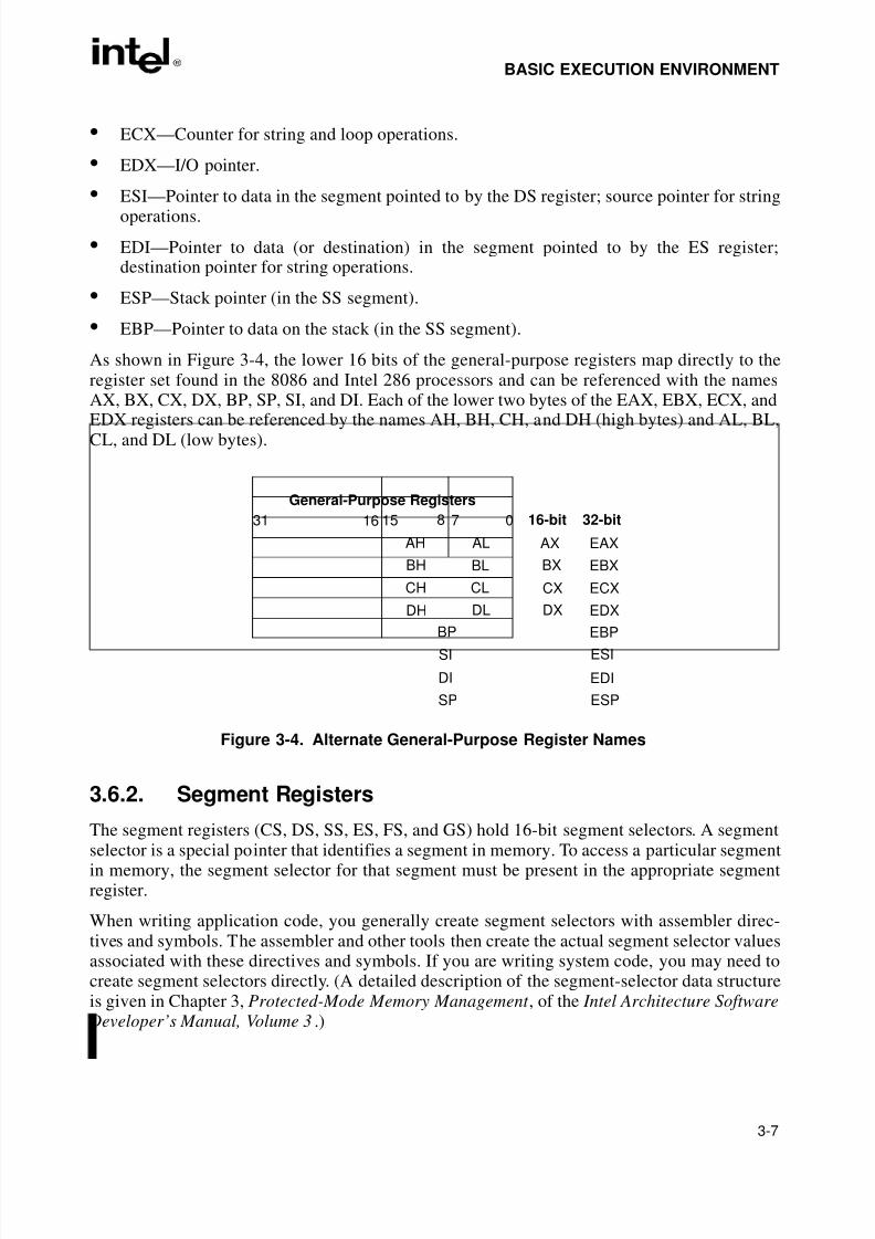
8/3/2019 Intel Architecture Software Developer's Manual, Volume 1: Basic Architecture
http://slidepdf.com/reader/full/intel-architecture-software-developers-manual-volume-1-basic-architecture 47/283
3-7
BASIC EXECUTION ENVIRONMENT
• ECX—Counter for string and loop operations.
• EDX—I/O pointer.
• ESI—Pointer to data in the segment pointed to by the DS register; source pointer for string
operations.
• EDI—Pointer to data (or destination) in the segment pointed to by the ES register;destination pointer for string operations.
• ESP—Stack pointer (in the SS segment).
• EBP—Pointer to data on the stack (in the SS segment).
As shown in Figure 3-4, the lower 16 bits of the general-purpose registers map directly to theregister set found in the 8086 and Intel 286 processors and can be referenced with the namesAX, BX, CX, DX, BP, SP, SI, and DI. Each of the lower two bytes of the EAX, EBX, ECX, and
EDX registers can be referenced by the names AH, BH, CH, and DH (high bytes) and AL, BL,CL, and DL (low bytes).
3.6.2. Segment Registers
The segment registers (CS, DS, SS, ES, FS, and GS) hold 16-bit segment selectors. A segment
selector is a special pointer that identifies a segment in memory. To access a particular segmentin memory, the segment selector for that segment must be present in the appropriate segmentregister.
When writing application code, you generally create segment selectors with assembler direc-tives and symbols. The assembler and other tools then create the actual segment selector valuesassociated with these directives and symbols. If you are writing system code, you may need tocreate segment selectors directly. (A detailed description of the segment-selector data structureis given in Chapter 3, Protected-Mode Memory Management , of the Intel Architecture Software
Developer’s Manual, Volume 3 .)
Figure 3-4. Alternate General-Purpose Register Names
071531 16 8
AH AL
BH BL
CH CL
DH DL
BPSI
DI
SP
16-bit
AX
DX
CX
BX
32-bit
EAX
EBX
ECX
EDX
EBPESI
ESP
General-Purpose Registers
EDI
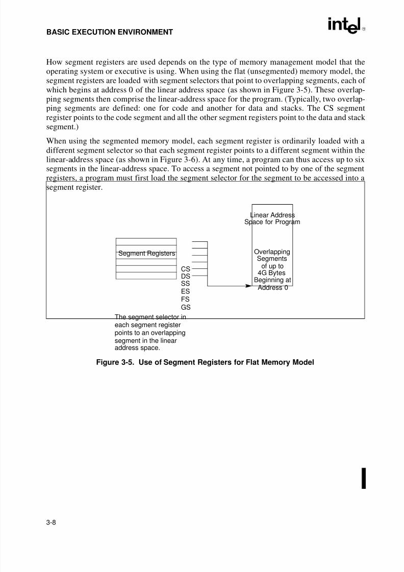
8/3/2019 Intel Architecture Software Developer's Manual, Volume 1: Basic Architecture
http://slidepdf.com/reader/full/intel-architecture-software-developers-manual-volume-1-basic-architecture 48/283
3-8
BASIC EXECUTION ENVIRONMENT
How segment registers are used depends on the type of memory management model that theoperating system or executive is using. When using the flat (unsegmented) memory model, thesegment registers are loaded with segment selectors that point to overlapping segments, each of which begins at address 0 of the linear address space (as shown in Figure 3-5). These overlap-
ping segments then comprise the linear-address space for the program. (Typically, two overlap-ping segments are defined: one for code and another for data and stacks. The CS segmentregister points to the code segment and all the other segment registers point to the data and stack segment.)
When using the segmented memory model, each segment register is ordinarily loaded with adifferent segment selector so that each segment register points to a different segment within thelinear-address space (as shown in Figure 3-6). At any time, a program can thus access up to sixsegments in the linear-address space. To access a segment not pointed to by one of the segmentregisters, a program must first load the segment selector for the segment to be accessed into asegment register.
Figure 3-5. Use of Segment Registers for Flat Memory Model
Segment Registers
CS
SSDS
ESFSGS
Linear AddressSpace for Program
The segment selector ineach segment registerpoints to an overlapping
OverlappingSegments
of up to4G Bytes
segment in the linearaddress space.
Beginning atAddress 0

8/3/2019 Intel Architecture Software Developer's Manual, Volume 1: Basic Architecture
http://slidepdf.com/reader/full/intel-architecture-software-developers-manual-volume-1-basic-architecture 49/283
3-9
BASIC EXECUTION ENVIRONMENT
Each of the segment registers is associated with one of three types of storage: code, data, orstack). For example, the CS register contains the segment selector for the code segment, wherethe instructions being executed are stored. The processor fetches instructions from the code
segment, using a logical address that consists of the segment selector in the CS register and thecontents of the EIP register. The EIP register contains the linear address within the code segmentof the next instruction to be executed. The CS register cannot be loaded explicitly by an appli-cation program. Instead, it is loaded implicitly by instructions or internal processor operationsthat change program control (such as, procedure calls, interrupt handling, or task switching).
The DS, ES, FS, and GS registers point to four data segments. The availability of four datasegments permits efficient and secure access to different types of data structures. For example,four separate data segments might be created: one for the data structures of the current module,another for the data exported from a higher-level module, a third for a dynamically created datastructure, and a fourth for data shared with another program. To access additional data segments,
the application program must load segment selectors for these segments into the DS, ES, FS, andGS registers, as needed.
The SS register contains the segment selector for a stack segment, where the procedure stack isstored for the program, task, or handler currently being executed. All stack operations use theSS register to find the stack segment. Unlike the CS register, the SS register can be loaded explic-itly, which permits application programs to set up multiple stacks and switch among them.
See Section 3.3., “Memory Organization”, for an overview of how the segment registers are usedin real-address mode.
Figure 3-6. Use of Segment Registers in Segmented Memory Model
Segment Registers
CSDSSSESFSGS
CodeSegment
DataSegment
StackSegment
DataSegment
DataSegment
DataSegment
All segmentsare mappedto the samelinear-addressspace
8/3/2019 Intel Architecture Software Developer's Manual, Volume 1: Basic Architecture
http://slidepdf.com/reader/full/intel-architecture-software-developers-manual-volume-1-basic-architecture 50/283
3-10
BASIC EXECUTION ENVIRONMENT
The four segment registers CS, DS, SS, and ES are the same as the segment registers found inthe Intel 8086 and Intel 286 processors and the FS and GS registers were introduced into theIntel Architecture with the Intel386 family of processors.
3.6.3. EFLAGS Register
The 32-bit EFLAGS register contains a group of status flags, a control flag, and a group of system flags. Figure 3-7 defines the flags within this register. Following initialization of theprocessor (either by asserting the RESET pin or the INIT pin), the state of the EFLAGS registeris 00000002H. Bits 1, 3, 5, 15, and 22 through 31 of this register are reserved. Software shouldnot use or depend on the states of any of these bits.
Some of the flags in the EFLAGS register can be modified directly, using special-purposeinstructions (described in the following sections). There are no instructions that allow the whole
register to be examined or modified directly. However, the following instructions can be used tomove groups of flags to and from the procedure stack or the EAX register: LAHF, SAHF,PUSHF, PUSHFD, POPF, and POPFD. After the contents of the EFLAGS register have beentransferred to the procedure stack or EAX register, the flags can be examined and modified usingthe processor’s bit manipulation instructions (BT, BTS, BTR, and BTC).
When suspending a task (using the processor’s multitasking facilities), the processor automati-cally saves the state of the EFLAGS register in the task state segment (TSS) for the task beingsuspended. When binding itself to a new task, the processor loads the EFLAGS register withdata from the new task’s TSS.
When a call is made to an interrupt or exception handler procedure, the processor automaticallysaves the state of the EFLAGS registers on the procedure stack. When an interrupt or exceptionis handled with a task switch, the state of the EFLAGS register is saved in the TSS for the task being suspended.
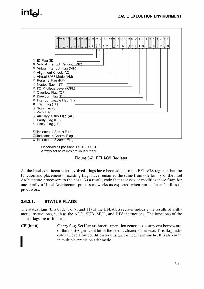
8/3/2019 Intel Architecture Software Developer's Manual, Volume 1: Basic Architecture
http://slidepdf.com/reader/full/intel-architecture-software-developers-manual-volume-1-basic-architecture 51/283
3-11
BASIC EXECUTION ENVIRONMENT
As the Intel Architecture has evolved, flags have been added to the EFLAGS register, but thefunction and placement of existing flags have remained the same from one family of the IntelArchitecture processors to the next. As a result, code that accesses or modifies these flags forone family of Intel Architecture processors works as expected when run on later families of processors.
3.6.3.1. STATUS FLAGS
The status flags (bits 0, 2, 4, 6, 7, and 11) of the EFLAGS register indicate the results of arith-metic instructions, such as the ADD, SUB, MUL, and DIV instructions. The functions of thestatus flags are as follows:
CF (bit 0) Carry flag. Set if an arithmetic operation generates a carry or a borrow outof the most-significant bit of the result; cleared otherwise. This flag indi-cates an overflow condition for unsigned-integer arithmetic. It is also usedin multiple-precision arithmetic.
Figure 3-7. EFLAGS Register
31 2930 28 27 26 25 24 23 22 21 20 19 18 1716
0R
F
I
D
A
C
V
M
X Virtual-8086 Mode (VM)X Resume Flag (RF)X Nested Task (NT)X I/O Privilege Level (IOPL)X Overflow Flag (OF)X Direction Flag (DF)X Interrupt Enable Flag (IF)
X Alignment Check (AC)
X ID Flag (ID)X Virtual Interrupt Pending (VIP)
15 1314 12 11 10 9 8 7 6 5 4 3 2 1 0
0 C
F
A
F
P
F1
D
F
I
F
T
F
S
F
Z
F
N
T000 0 0 0 0 0 0 0 0
VI
P
VI
F
O
F
IO
PL
X Virtual Interrupt Flag (VIF)
X Trap Flag (TF)S Sign Flag (SF)S Zero Flag (ZF)S Auxiliary Carry Flag (AF)S Parity Flag (PF)S Carry Flag (CF)
S Indicates a Status FlagC Indicates a Control FlagX Indicates a System Flag
Reserved bit positions. DO NOT USE.Always set to values previously read.
8/3/2019 Intel Architecture Software Developer's Manual, Volume 1: Basic Architecture
http://slidepdf.com/reader/full/intel-architecture-software-developers-manual-volume-1-basic-architecture 52/283
3-12
BASIC EXECUTION ENVIRONMENT
PF (bit 2) Parity flag. Set if the least-significant byte of the result contains an evennumber of 1 bits; cleared otherwise.
AF (bit 4) Adjust flag. Set if an arithmetic operation generates a carry or a borrow
out of bit 3 of the result; cleared otherwise. This flag is used in binary-coded decimal (BCD) arithmetic.
ZF (bit 6) Zero flag. Set if the result is zero; cleared otherwise.
SF (bit 7) Sign flag. Set equal to the most-significant bit of the result, which is thesign bit of a signed integer. (0 indicates a positive value and 1 indicates anegative value.)
OF (bit 11) Overflow flag. Set if the integer result is too large a positive number ortoo small a negative number (excluding the sign-bit) to fit in the destina-tion operand; cleared otherwise. This flag indicates an overflow condition
for signed-integer (two’s complement) arithmetic.Of these status flags, only the CF flag can be modified directly, using the STC, CLC, and CMCinstructions. Also the bit instructions (BT, BTS, BTR, and BTC) copy a specified bit into the CFflag.
The status flags allow a single arithmetic operation to produce results for three different datatypes: unsigned integers, signed integers, and BCD integers. If the result of an arithmetic oper-ation is treated as an unsigned integer, the CF flag indicates an out-of-range condition (carry ora borrow); if treated as a signed integer (two’s complement number), the OF flag indicates acarry or borrow; and if treated as a BCD digit, the AF flag indicates a carry or borrow. The SFflag indicates the sign of a signed integer. The ZF flag indicates either a signed- or an unsigned-
integer zero.
When performing multiple-precision arithmetic on integers, the CF flag is used in conjunctionwith the add with carry (ADC) and subtract with borrow (SBB) instructions to propagate a carryor borrow from one computation to the next.
The condition instructions Jcc (jump on condition code cc), SETcc (byte set on condition codecc), LOOPcc, and CMOVcc (conditional move) use one or more of the status flags as conditioncodes and test them for branch, set-byte, or end-loop conditions.
3.6.3.2. DF FLAG
The direction flag (DF, located in bit 10 of the EFLAGS register) controls the string instructions(MOVS, CMPS, SCAS, LODS, and STOS). Setting the DF flag causes the string instructions toauto-decrement (that is, to process strings from high addresses to low addresses). Clearing theDF flag causes the string instructions to auto-increment (process strings from low addressesto high addresses).
The STD and CLD instructions set and clear the DF flag, respectively.
8/3/2019 Intel Architecture Software Developer's Manual, Volume 1: Basic Architecture
http://slidepdf.com/reader/full/intel-architecture-software-developers-manual-volume-1-basic-architecture 53/283
3-13
BASIC EXECUTION ENVIRONMENT
3.6.4. System Flags and IOPL Field
The system flags and IOPL field in the EFLAGS register control operating-system or executiveoperations. They should not be modified by application programs. The functions of the status
flags are as follows:
IF (bit 9) Interrupt enable flag. Controls the response of the processor tomaskable interrupt requests. Set to respond to maskable interrupts;cleared to inhibit maskable interrupts.
TF (bit 8) Trap flag. Set to enable single-step mode for debugging; clear todisable single-step mode.
IOPL (bits 12 and 13) I/O privilege level field. Indicates the I/O privilege level of thecurrently running program or task. The current privilege level (CPL)of the currently running program or task must be less than or equal to
the I/O privilege level to access the I/O address space. This field canonly be modified by the POPF and IRET instructions when operatingat a CPL of 0.
NT (bit 14) Nested task flag. Controls the chaining of interrupted and calledtasks. Set when the current task is linked to the previously executedtask; cleared when the current task is not linked to another task.
RF (bit 16) Resume flag. Controls the processor’s response to debug exceptions.
VM (bit 17) Virtual-8086 mode flag. Set to enable virtual-8086 mode; clear toreturn to protected mode.
AC (bit 18) Alignment check flag. Set this flag and the AM bit in the CR0register to enable alignment checking of memory references; clearthe AC flag and/or the AM bit to disable alignment checking.
VIF (bit 19) Virtual interrupt flag. Virtual image of the IF flag. Used in conjunc-tion with the VIP flag. (To use this flag and the VIP flag the virtualmode extensions are enabled by setting the VME flag in controlregister CR4.)
VIP (bit 20) Virtual interrupt pending flag. Set to indicate to that an interrupt ispending; clear when no interrupts are pending. (Software sets and
clears this flag. The processor only reads it.) Used in conjunctionwith the VIF flag.
ID (bit 21) Identification flag. The ability of a program to set or clear this flagindicates support for the CPUID instruction.
See Chapter 3, Protected-Mode Memory Management , in the Intel Architecture Software Devel-oper’s Manual, Volume 3, for a detail description of these flags.
8/3/2019 Intel Architecture Software Developer's Manual, Volume 1: Basic Architecture
http://slidepdf.com/reader/full/intel-architecture-software-developers-manual-volume-1-basic-architecture 54/283
3-14
BASIC EXECUTION ENVIRONMENT
3.7. INSTRUCTION POINTER
The instruction pointer (EIP) register contains the offset in the current code segment for the nextinstruction to be executed. It is advanced from one instruction boundary to the next in straight-
line code or it is moved ahead or backwards by a number of instructions when executing JMP,Jcc, CALL, RET, and IRET instructions.
The EIP register cannot be accessed directly by software; it is controlled implicitly by control-transfer instructions (such as JMP, Jcc, CALL, and RET), interrupts, and exceptions. The onlyway to read the EIP register is to execute a CALL instruction and then read the value of the returninstruction pointer from the procedure stack. The EIP register can be loaded indirectly by modi-fying the value of a return instruction pointer on the procedure stack and executing a returninstruction (RET or IRET). See Section 4.2.4.2., “Return Instruction Pointer”.
All Intel Architecture processors prefetch instructions. Because of instruction prefetching, aninstruction address read from the bus during an instruction load does not match the value in theEIP register. Even though different processor generations use different prefetching mechanisms,the function of EIP register to direct program flow remains fully compatible with all softwarewritten to run on Intel Architecture processors.
3.8. OPERAND-SIZE AND ADDRESS-SIZE ATTRIBUTES
When processor is executing in protected mode, every code segment has a default operand-sizeattribute and address-size attribute. These attributes are selected with the D (default size) flag inthe segment descriptor for the code segment (see Chapter 3, Protected-Mode Memory Manage-
ment , in the Intel Architecture Software Developer’s Manual, Volume 3). When the D flag is set,the 32-bit operand-size and address-size attributes are selected; when the flag is clear, the 16-bitsize attributes are selected. When the processor is executing in real-address mode, virtual-8086mode, or SMM, the default operand-size and address-size attributes are always 16 bits.
The operand-size attribute selects the sizes of operands that instructions operate on. When the16-bit operand-size attribute is in force, operands can generally be either 8 bits or 16 bits, andwhen the 32-bit operand-size attribute is in force, operands can generally be 8 bits or 32 bits.
The address-size attribute selects the sizes of addresses used to address memory: 16 bits or 32bits. When the 16-bit address-size attribute is in force, segment offsets and displacements are16-bits. This restriction limits the size of a segment that can be addressed to 64 KBytes. When
the 32-bit address-size attribute is in force, segment offsets and displacements are 32-bits,allowing segments of up to 4 GBytes to be addressed.
The default operand-size attribute and/or address-size attribute can be overridden for a partic-ular instruction by adding an operand-size and/or address-size prefix to an instruction (see“Instruction Prefixes” in Chapter 2 of the Intel Architecture Software Developer’s Manual,Volume 3). The effect of this prefix applies only to the instruction it is attached to.
Table 3-1 shows effective operand size and address size (when executing in protected mode)depending on the settings of the B flag and the operand-size and address-size prefixes.
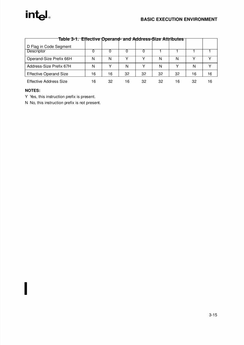
8/3/2019 Intel Architecture Software Developer's Manual, Volume 1: Basic Architecture
http://slidepdf.com/reader/full/intel-architecture-software-developers-manual-volume-1-basic-architecture 55/283
3-15
BASIC EXECUTION ENVIRONMENT
NOTES:
Y Yes, this instruction prefix is present.
N No, this instruction prefix is not present.
Table 3-1. Effective Operand- and Address-Size Attributes
D Flag in Code SegmentDescriptor 0 0 0 0 1 1 1 1
Operand-Size Prefix 66H N N Y Y N N Y Y
Address-Size Prefix 67H N Y N Y N Y N Y
Effective Operand Size 16 16 32 32 32 32 16 16
Effective Address Size 16 32 16 32 32 16 32 16

8/3/2019 Intel Architecture Software Developer's Manual, Volume 1: Basic Architecture
http://slidepdf.com/reader/full/intel-architecture-software-developers-manual-volume-1-basic-architecture 56/283
8/3/2019 Intel Architecture Software Developer's Manual, Volume 1: Basic Architecture
http://slidepdf.com/reader/full/intel-architecture-software-developers-manual-volume-1-basic-architecture 57/283
4Procedure Calls,Interrupts, and
Exceptions

8/3/2019 Intel Architecture Software Developer's Manual, Volume 1: Basic Architecture
http://slidepdf.com/reader/full/intel-architecture-software-developers-manual-volume-1-basic-architecture 58/283
8/3/2019 Intel Architecture Software Developer's Manual, Volume 1: Basic Architecture
http://slidepdf.com/reader/full/intel-architecture-software-developers-manual-volume-1-basic-architecture 59/283
4-1
CHAPTER 4PROCEDURE CALLS, INTERRUPTS, AND
EXCEPTIONS
This chapter describes the facilities in the Intel Architecture for executing calls to procedures orsubroutines. It also describes how interrupts and exceptions are handled from the perspective of an application programmer.
4.1. PROCEDURE CALL TYPES
The processor supports procedure calls in two different ways:
• CALL and RET instructions.
• ENTER and LEAVE instructions, in conjunction with the CALL and RET instructions.
Both of these procedure call mechanisms use the procedure stack, commonly referred to simplyas “the stack,” to save the state of the calling procedure, pass parameters to the called procedure,and store local variables for the currently executing procedure.
The processor’s facilities for handling interrupts and exceptions are similar to those used by theCALL and RET instructions.
4.2. STACK
The stack (see Figure 4-1) is a contiguous array of memory locations. It is contained in asegment and identified by the segment selector in the SS register. (When using the flat memorymodel, the stack can be located anywhere in the linear address space for the program.) A stack can be up to 4 gigabytes long, the maximum size of a segment.
The next available memory location on the stack is called the top of stack. At any given time,the stack pointer (contained in the ESP register) gives the address (that is the offset from the base
of the SS segment) of the top of the stack.
Items are placed on the stack using the PUSH instruction and removed from the stack using thePOP instruction. When an item is pushed onto the stack, the processor decrements the ESPregister, then writes the item at the new top of stack. When an item is popped off the stack, theprocessor reads the item from the top of stack, then increments the ESP register. In this manner,the stack grows down in memory (towards lesser addresses) when items are pushed on the stack and shrinks up (towards greater addresses) when the items are popped from the stack.
A program or operating system/executive can set up many stacks. For example, in multitaskingsystems, each task can be given its own stack. The number of stacks in a system is limited by themaximum number of segments and the available physical memory. When a system sets up many
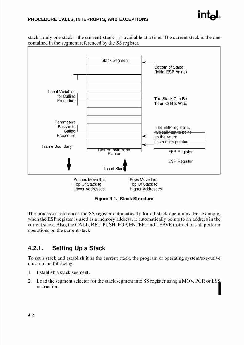
8/3/2019 Intel Architecture Software Developer's Manual, Volume 1: Basic Architecture
http://slidepdf.com/reader/full/intel-architecture-software-developers-manual-volume-1-basic-architecture 60/283
4-2
PROCEDURE CALLS, INTERRUPTS, AND EXCEPTIONS
stacks, only one stack—the current stack—is available at a time. The current stack is the onecontained in the segment referenced by the SS register.
The processor references the SS register automatically for all stack operations. For example,when the ESP register is used as a memory address, it automatically points to an address in thecurrent stack. Also, the CALL, RET, PUSH, POP, ENTER, and LEAVE instructions all performoperations on the current stack.
4.2.1. Setting Up a Stack
To set a stack and establish it as the current stack, the program or operating system/executivemust do the following:
1. Establish a stack segment.
2. Load the segment selector for the stack segment into SS register using a MOV, POP, or LSSinstruction.
Figure 4-1. Stack Structure
Bottom of Stack(Initial ESP Value)
Local Variablesfor CallingProcedure
ParametersPassed to
CalledProcedure
Frame Boundary
EBP Register
ESP Register
Return Instruction
Top of Stack
Stack Segment
Pushes Move theTop Of Stack toLower Addresses
Pops Move theTop Of Stack toHigher Addresses
The EBP register is
The Stack Can Be16 or 32 Bits Wide
typically set to pointto the returninstruction pointer.
Pointer
8/3/2019 Intel Architecture Software Developer's Manual, Volume 1: Basic Architecture
http://slidepdf.com/reader/full/intel-architecture-software-developers-manual-volume-1-basic-architecture 61/283
4-3
PROCEDURE CALLS, INTERRUPTS, AND EXCEPTIONS
3. Load the stack pointer for the stack into the ESP register using a MOV, POP, or LSSinstruction. (The LSS instruction can be used to load the SS and ESP registers in oneoperation.)
See “Segment Descriptors” in Chapter 3 of the Intel Architecture Software Developer’s Manual,Volume 3, for information on how to set up a segment descriptor and segment limits for a stack segment.
4.2.2. Stack Alignment
The stack pointer for a stack segment should be aligned on 16-bit (word) or 32-bit (double-word)boundaries, depending on the width of the stack segment. The D flag in the segment descriptorfor the current code segment sets the stack-segment width (see “Segment Descriptors” in Chap-ter 3 of the Intel Architecture Software Developer’s Manual, Volume 3). The PUSH and POP in-
structions use the D flag to determine how much to decrement or increment the stack pointer ona push or pop operation, respectively. When the stack width is 16 bits, the stack pointer is incre-mented or decremented in 16-bit increments; when the width is 32 bits, the stack pointer is in-cremented or decremented in 32-bit increments. If a 16-bit value is pushed onto a 32-bit widestack, the value is automatically padded with zeros out to 32 bits.
The processor does not check stack pointer alignment. It is the responsibility of the programs,tasks, and system procedures running on the processor to maintain proper alignment of stack pointers. Misaligning a stack pointer can cause serious performance degradation and in someinstances program failures.
4.2.3. Address-Size Attributes for Stack Accesses
Instructions that use the stack implicitly (such as the PUSH and POP instructions) have twoaddress-size attributes each of either 16 or 32 bits. This is because they always have the implicitaddress of the top of the stack, and they may also have an explicit memory address (for example,PUSH Array1[EBX]). The attribute of the explicit address is determined by the D flag of thecurrent code segment and the presence or absence of the 67H address-size prefix, as usual.
The address-size attribute of the top of the stack determines whether SP or ESP is used for thestack access. Stack operations with an address-size attribute of 16 use the 16-bit SP stack pointer
register and can use a maximum stack address of FFFFH; stack operations with a address-sizeattribute of 32 bits use the 32-bit ESP register and can use a maximum address of FFFFFFFFH.The default address-size attribute for data segments used as stacks is controlled by the B flag of the segment’s descriptor. When this flag is clear, the default address-size attribute is 16; whenthe flag is set, the address-size attribute is 32.
4.2.4. Procedure Linking Information
The processor provides two pointers for linking of procedures: the stack-frame base pointer andthe return instruction pointer. When used in conjunction with a standard software procedure-call
technique, these pointers permit reliable and coherent linking of procedures
8/3/2019 Intel Architecture Software Developer's Manual, Volume 1: Basic Architecture
http://slidepdf.com/reader/full/intel-architecture-software-developers-manual-volume-1-basic-architecture 62/283
4-4
PROCEDURE CALLS, INTERRUPTS, AND EXCEPTIONS
4.2.4.1. STACK-FRAME BASE POINTER
The stack is typically divided into frames. Each stack frame can then contain local variables,parameters to be passed to another procedure, and procedure linking information. The stack-
frame base pointer (contained in the EBP register) identifies a fixed reference point within thestack frame for the called procedure. To use the stack-frame base pointer, the called proceduretypically copies the contents of the ESP register into the EBP register prior to pushing any localvariables on the stack. The stack-frame base pointer then permits easy access to data structurespassed on the stack, to the return instruction pointer, and to local variables added to the stack bythe called procedure.
Like the ESP register, the EBP register automatically points to an address in the current stack segment (that is, the segment specified by the current contents of the SS register).
4.2.4.2. RETURN INSTRUCTION POINTER
Prior to branching to the first instruction of the called procedure, the CALL instruction pushesthe address in the EIP register onto the current stack. This address is then called the return-instruction pointer and it points to the instruction where execution of the calling procedureshould resume following a return from the called procedure. Upon returning from a calledprocedure, the RET instruction pops the return-instruction pointer from the stack back into theEIP register. Execution of the calling procedure then resumes.
The processor does not keep track of the location of the return-instruction pointer. It is thus upto the programmer to insure that stack pointer is pointing to the return-instruction pointer on thestack, prior to issuing a RET instruction. A common way to reset the stack pointer to the point
to the return-instruction pointer is to move the contents of the EBP register into the ESP register.If the EBP register is loaded with the stack pointer immediately following a procedure call, itshould point to the return instruction pointer on the stack.
The processor does not require that the return instruction pointer point back to the calling proce-dure. Prior to executing the RET instruction, the return instruction pointer can be manipulatedin software to point to any address in the current code segment (near return) or another codesegment (far return). Performing such an operation, however, should be undertaken verycautiously, using only well defined code entry points.
4.3. CALLING PROCEDURES USING CALL AND RETThe CALL instructions allows control transfers to procedures within the current code segment(near call) and in a different code segment (far call). Near calls usually provide access to localprocedures within the currently running program or task. Far calls are usually used to accessoperating system procedures or procedures in a different task. See “CALL—Call Procedure” inChapter 3 of the Intel Architecture Software Developer’s Manual, Volume 2, for a detaileddescription of the CALL instruction.
The RET instruction also allows near and far returns to match the near and far versions of theCALL instruction. In addition, the RET instruction allows a program to increment the stack
pointer on a return to release parameters from the stack. The number of bytes released from the
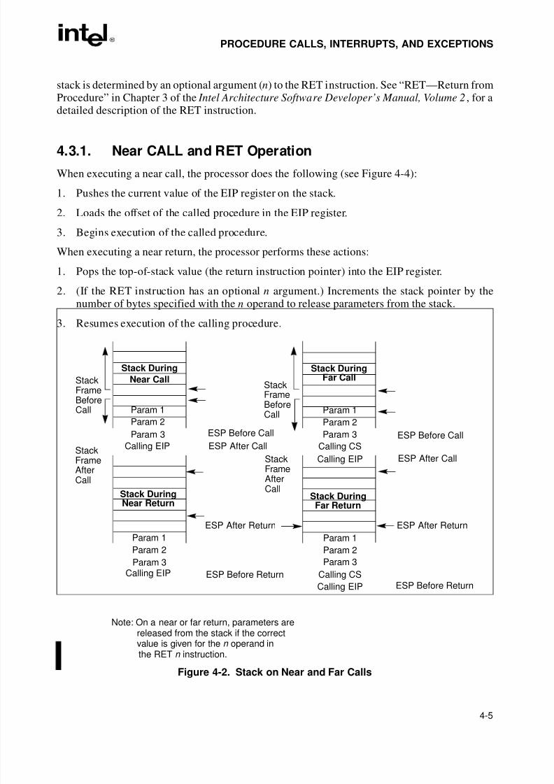
8/3/2019 Intel Architecture Software Developer's Manual, Volume 1: Basic Architecture
http://slidepdf.com/reader/full/intel-architecture-software-developers-manual-volume-1-basic-architecture 63/283
4-5
PROCEDURE CALLS, INTERRUPTS, AND EXCEPTIONS
stack is determined by an optional argument (n) to the RET instruction. See “RET—Return fromProcedure” in Chapter 3 of the Intel Architecture Software Developer’s Manual, Volume 2 , for adetailed description of the RET instruction.
4.3.1. Near CALL and RET Operation
When executing a near call, the processor does the following (see Figure 4-4):
1. Pushes the current value of the EIP register on the stack.
2. Loads the offset of the called procedure in the EIP register.
3. Begins execution of the called procedure.
When executing a near return, the processor performs these actions:
1. Pops the top-of-stack value (the return instruction pointer) into the EIP register.
2. (If the RET instruction has an optional n argument.) Increments the stack pointer by thenumber of bytes specified with the n operand to release parameters from the stack.
3. Resumes execution of the calling procedure.
Figure 4-2. Stack on Near and Far Calls
Param 1
Param 2
ESP Before Call
Stack During
Near CallStack During
Far Call
Calling CS
Param 1
Param 2
Calling EIP
Param 3 Param 3
ESP After Return
Calling CS
Param 1Param 2
Calling EIP
Param 3
Param 1Param 2
Param 3
Note: On a near or far return, parameters are
Calling EIP ESP After Call
Stack DuringNear Return
Calling EIP
released from the stack if the correctvalue is given for the n operand inthe RET n instruction.
ESP Before Return
ESP Before Call
ESP After Call
ESP Before Return
ESP After Return
Stack DuringFar Return
StackFrame
BeforeCall
StackFrame
BeforeCall
StackFrameAfterCall
StackFrameAfterCall
8/3/2019 Intel Architecture Software Developer's Manual, Volume 1: Basic Architecture
http://slidepdf.com/reader/full/intel-architecture-software-developers-manual-volume-1-basic-architecture 64/283
4-6
PROCEDURE CALLS, INTERRUPTS, AND EXCEPTIONS
4.3.2. Far CALL and RET Operation
When executing a far call, the processor performs these actions (see Figure 4-4):
1. Pushes current value of the CS register on the stack.
2. Pushes the current value of the EIP register on the stack.
3. Loads the segment selector of the segment that contains the called procedure in the CSregister.
4. Loads the offset of the called procedure in the EIP register.
5. Begins execution of the called procedure.
When executing a far return, the processor does the following:
1. Pops the top-of-stack value (the return instruction pointer) into the EIP register.
2. Pops the top-of-stack value (the segment selector for the code segment being returned to)into the CS register.
3. (If the RET instruction has an optional n argument.) Increments the stack pointer by thenumber of bytes specified with the n operand to release parameters from the stack.
4. Resumes execution of the calling procedure.
4.3.3. Parameter Passing
Parameters can be passed between procedures in any of three ways: through general-purposeregisters, in an argument list, or on the stack.
4.3.3.1. PASSING PARAMETERS THROUGH THE GENERAL-PURPOSE
REGISTERS
The processor does not save the state of the general-purpose registers on procedure calls. Acalling procedure can thus pass up to six parameter to the called procedure by copying theparameters into any of these registers (except the ESP and EBP registers) prior to executing theCALL instruction. The called procedure can likewise pass parameters back to the calling proce-
dure through general-purpose registers.
4.3.3.2. PASSING PARAMETERS ON THE STACK
To pass a large number of parameters to the called procedure, the parameters can be placed onthe stack, in the stack frame for the calling procedure. Here, it is useful to use the stack-framebase pointer (in the EBP register) to make a frame boundary for easy access to the parameters.
The stack can also be used to pass parameters back from the called procedure to the callingprocedure.
8/3/2019 Intel Architecture Software Developer's Manual, Volume 1: Basic Architecture
http://slidepdf.com/reader/full/intel-architecture-software-developers-manual-volume-1-basic-architecture 65/283
4-7
PROCEDURE CALLS, INTERRUPTS, AND EXCEPTIONS
4.3.3.3. PASSING PARAMETERS IN AN ARGUMENT LIST
An alternate method of passing a larger number of parameters (or a data structure) to the calledprocedure is to place the parameters in an argument list in one of the data segments in memory.
A pointer to the argument list can then be passed to the called procedure through a general-purpose register or the stack. Parameters can also be passed back to the calling procedure in thissame manner.
4.3.4. Saving Procedure State Information
The processor does not save the contents of the general-purpose registers, segment registers, orthe EFLAGS register on a procedure call. A calling procedure should explicitly save the valuesin any of the general-purpose registers that it will need when it resumes execution after a return.These values can be saved on the stack or in memory in one of the data segments.
The PUSHA and POPA instruction facilitates saving and restoring the contents of the general-purpose registers. PUSHA pushes the values in all the general-purpose registers on the stack inthe following order: EAX, ECX, EDX, EBX, ESP (the value prior to executing the PUSHAinstruction), EBP, ESI, and EDI. The POPA instruction pops all the register values saved with aPUSHA instruction (except the ESI value) from the stack to their respective registers.
If a called procedure changes the state of any of the segment registers explicitly, it should restorethem to their former value before executing a return to the calling procedure.
If a calling procedure needs to maintain the state of the EFLAGS register it can save and restoreall or part of the register using the PUSHF/PUSHFD and POPF/POPFD instructions. The
PUSHF instruction pushes the lower word of the EFLAGS register on the stack, while thePUSHFD instruction pushes the entire register. The POPF instruction pops a word from thestack into the lower word of the EFLAGS register, while the POPFD instruction pops a doubleword from the stack into the register.
4.3.5. Calls to Other Privilege Levels
The Intel Architecture’s protection mechanism recognizes four privilege levels, numbered from0 to 3, where greater numbers mean lesser privileges. The primary reason to use these privilegelevels is to improve the reliability of operating systems. For example, Figure 4-3 shows howprivilege levels can be interpreted as rings of protection.
In this example, the highest privilege level 0 (at the center of the diagram) is used for segmentsthat contain the most critical code modules in the system, usually the kernel of an operatingsystem. The outer rings (with progressively lower privileges) are used for segments that containcode modules for less critical software.
Code modules in lower privilege segments can only access modules operating at higher privilegesegments by means of a tightly controlled and protected interface called a gate. Attempts toaccess higher privilege segments without going through a protection gate and without havingsufficient access rights causes a general-protection exception (#GP) to be generated.
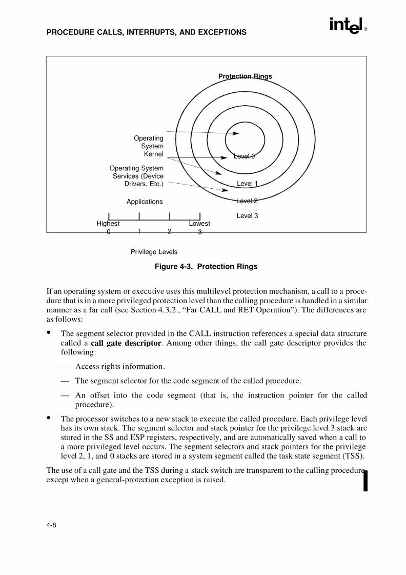
8/3/2019 Intel Architecture Software Developer's Manual, Volume 1: Basic Architecture
http://slidepdf.com/reader/full/intel-architecture-software-developers-manual-volume-1-basic-architecture 66/283
4-8
PROCEDURE CALLS, INTERRUPTS, AND EXCEPTIONS
If an operating system or executive uses this multilevel protection mechanism, a call to a proce-dure that is in a more privileged protection level than the calling procedure is handled in a similarmanner as a far call (see Section 4.3.2., “Far CALL and RET Operation”). The differences areas follows:
• The segment selector provided in the CALL instruction references a special data structurecalled a call gate descriptor. Among other things, the call gate descriptor provides thefollowing:
— Access rights information.
— The segment selector for the code segment of the called procedure.
— An offset into the code segment (that is, the instruction pointer for the calledprocedure).
• The processor switches to a new stack to execute the called procedure. Each privilege levelhas its own stack. The segment selector and stack pointer for the privilege level 3 stack arestored in the SS and ESP registers, respectively, and are automatically saved when a call toa more privileged level occurs. The segment selectors and stack pointers for the privilegelevel 2, 1, and 0 stacks are stored in a system segment called the task state segment (TSS).
The use of a call gate and the TSS during a stack switch are transparent to the calling procedure,except when a general-protection exception is raised.
Figure 4-3. Protection Rings
Level 0
Level 1
Level 2
Level 3
Protection Rings
Operating
Operating SystemServices (Device
Drivers, Etc.)
Applications
0 1 2 3
Highest Lowest
Privilege Levels
SystemKernel
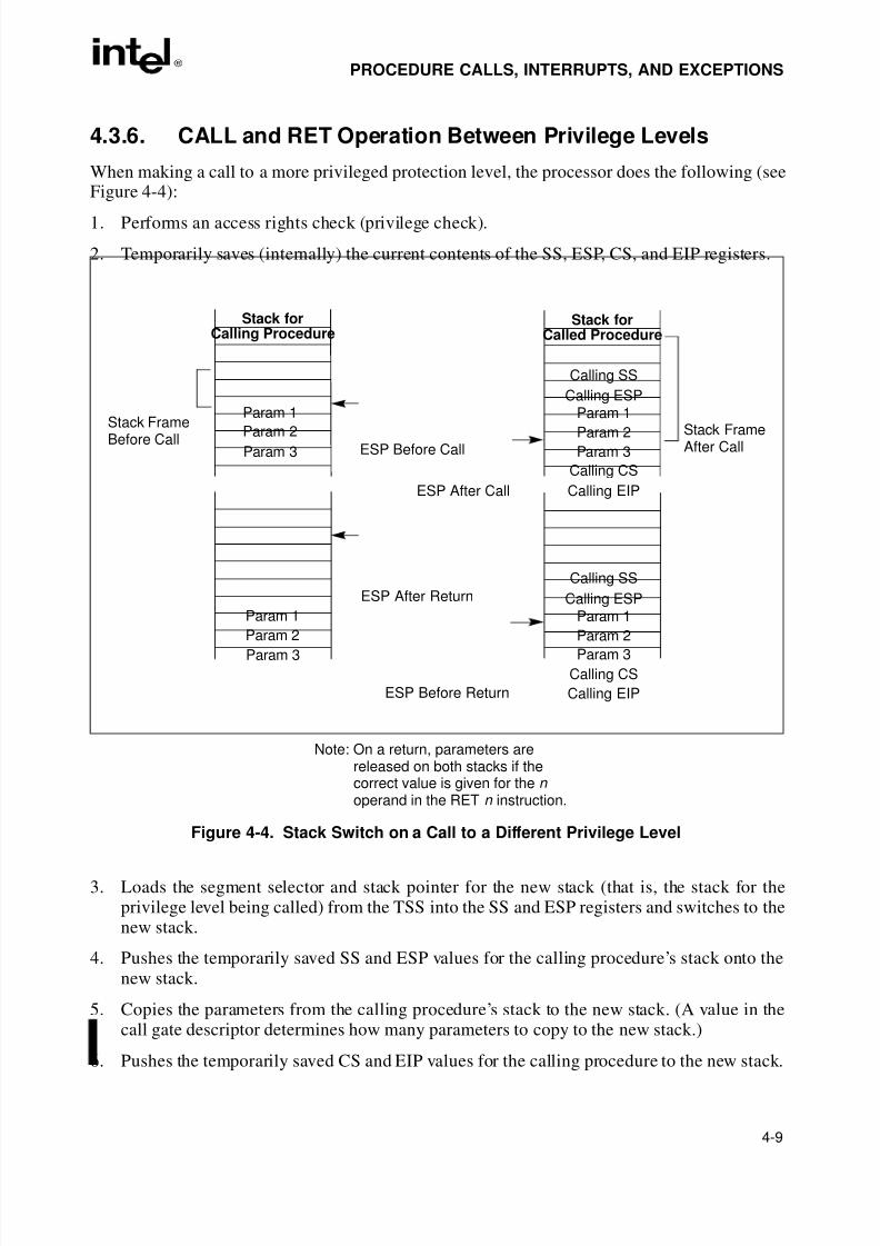
8/3/2019 Intel Architecture Software Developer's Manual, Volume 1: Basic Architecture
http://slidepdf.com/reader/full/intel-architecture-software-developers-manual-volume-1-basic-architecture 67/283
4-9
PROCEDURE CALLS, INTERRUPTS, AND EXCEPTIONS
4.3.6. CALL and RET Operation Between Privilege Levels
When making a call to a more privileged protection level, the processor does the following (seeFigure 4-4):
1. Performs an access rights check (privilege check).
2. Temporarily saves (internally) the current contents of the SS, ESP, CS, and EIP registers.
3. Loads the segment selector and stack pointer for the new stack (that is, the stack for theprivilege level being called) from the TSS into the SS and ESP registers and switches to thenew stack.
4. Pushes the temporarily saved SS and ESP values for the calling procedure’s stack onto thenew stack.
5. Copies the parameters from the calling procedure’s stack to the new stack. (A value in thecall gate descriptor determines how many parameters to copy to the new stack.)
6. Pushes the temporarily saved CS and EIP values for the calling procedure to the new stack.
Figure 4-4. Stack Switch on a Call to a Different Privilege Level
Param 1
Param 2ESP Before Call
Stack forCalling Procedure
ESP After Call
Stack forCalled Procedure
Calling SS
Calling ESP
Calling CS
Param 1
Param 2
Calling EIP
Stack FrameBefore Call Stack FrameAfter CallParam 3 Param 3
ESP After Return
ESP Before Return
Calling SS
Calling ESP
Calling CS
Param 1
Param 2
Calling EIP
Param 3
Param 1
Param 2Param 3
Note: On a return, parameters arereleased on both stacks if thecorrect value is given for the n
operand in the RET n instruction.
8/3/2019 Intel Architecture Software Developer's Manual, Volume 1: Basic Architecture
http://slidepdf.com/reader/full/intel-architecture-software-developers-manual-volume-1-basic-architecture 68/283
4-10
PROCEDURE CALLS, INTERRUPTS, AND EXCEPTIONS
7. Loads the segment selector for the new code segment and the new instruction pointer fromthe call gate into the CS and EIP registers, respectively.
8. Begins execution of the called procedure at the new privilege level.
When executing a return from the privileged procedure, the processor performs these actions:
1. Performs a privilege check.
2. Restores the CS and EIP registers to their values prior to the call.
3. (If the RET instruction has an optional n argument.) Increments the stack pointer by thenumber of bytes specified with the n operand to release parameters from the stack. If thecall gate descriptor specifies that one or more parameters be copied from one stack to theother, a RET n instruction must be used to release the parameters from both stacks. Here,the n operand specifies the number of bytes occupied on each stack by the parameters. Ona return, the processor increments ESP by n for each stack to step over (effectively remove)
these parameters from the stacks.
4. Restores the SS and ESP registers to their values prior to the call, which causes a switchback to the stack of the calling procedure.
5. (If the RET instruction has an optional n argument.) Increments the stack pointer by thenumber of bytes specified with the n operand to release parameters from the stack (seeexplanation in step 3).
6. Resumes execution of the calling procedure.
See Chapter 4, Protection, in the Intel Architecture Software Developer’s Manual, Volume 3 , for
detailed information on calls to privileged levels and the call gate descriptor.
4.4. INTERRUPTS AND EXCEPTIONS
The processor provides two mechanisms for interrupting program execution: interrupts andexceptions:
• An interrupt is an asynchronous event that is typically triggered by an I/O device.
• An exception is a synchronous event that is generated when the processor detects one ormore predefined conditions while executing an instruction. The Intel architecture specifies
three classes of exceptions: faults, traps, and aborts.
The processor responds to interrupts and exceptions in essentially the same way. When an inter-rupt or exception is signaled, the processor halts execution of the current program or task andswitches to a handler procedure that has been written specifically to handle the interrupt orexception condition. The processor accesses the handler procedure through an entry in the inter-rupt descriptor table (IDT). When the handler has completed handling the interrupt or exception,program control is returned to the interrupted program or task.
The operating system, executive, and/or device drivers normally handle interrupts and excep-tions independently from application programs or tasks. Application programs can, however,
access the interrupt and exception handlers incorporated in an operating system or executive
8/3/2019 Intel Architecture Software Developer's Manual, Volume 1: Basic Architecture
http://slidepdf.com/reader/full/intel-architecture-software-developers-manual-volume-1-basic-architecture 69/283
4-11
PROCEDURE CALLS, INTERRUPTS, AND EXCEPTIONS
through assembly-language calls. The remainder of this section gives a brief overview of theprocessor’s interrupt and exception handling mechanism. See Chapter 5, Interrupt and Excep-
tion Handling in the Intel Architecture Software Developer’s Manual, Volume 3, for a detaileddescription of this mechanism.
The Intel Architecture defines 16 predefined interrupts and exceptions and 224 user definedinterrupts, which are associated with entries in the IDT. Each interrupt and exception in the IDTis identified with a number, called a vector. Table 4-1 lists the interrupts and exceptions withentries in the IDT and their respective vector numbers. Vectors 0 through 8, 10 through 14, and16 through 18 are the predefined interrupts and exceptions, and vectors 32 through 255 are theuser-defined interrupts, called maskable interrupts.
Note that the processor defines several additional interrupts that do not point to entries in theIDT; the most notable of these interrupts is the SMI interrupt. See “Exception and InterruptVectors” in Chapter 5 of the Intel Architecture Software Developer’s Manual, Volume 3 , for more
information about the interrupts and exceptions that the Intel Architecture supports.When the processor detects an interrupt or exception, it does one of the following things:
• Executes an implicit call to a handler procedure.
• Executes an implicit call to a handler task.
4.4.1. Call and Return Operation for Interrupt or ExceptionHandling Procedures
A call to an interrupt or exception handler procedure is similar to a procedure call to anotherprotection level (see Section 4.3.6., “CALL and RET Operation Between Privilege Levels”).Here, the interrupt vector references one of two kinds of gates: an interrupt gate or a trap gate.Interrupt and trap gates are similar to call gates in that they provide the following information:
• Access rights information.
• The segment selector for the code segment that contains the handler procedure.
• An offset into the code segment to the first instruction of the handler procedure.
The difference between an interrupt gate and a trap gate is as follows. If an interrupt or exceptionhandler is called through an interrupt gate, the processor clears the interrupt enable (IF) flag inthe EFLAGS register to prevent subsequent interrupts from interfering with the execution of thehandler. When a handler is called through a trap gate, the state of the IF flag is not changed.
If the code segment for the handler procedure has the same privilege level as the currentlyexecuting program or task, the handler procedure uses the current stack; if the handler executesat a more privileged level, the processor switches to the stack for the handler’s privilege level.
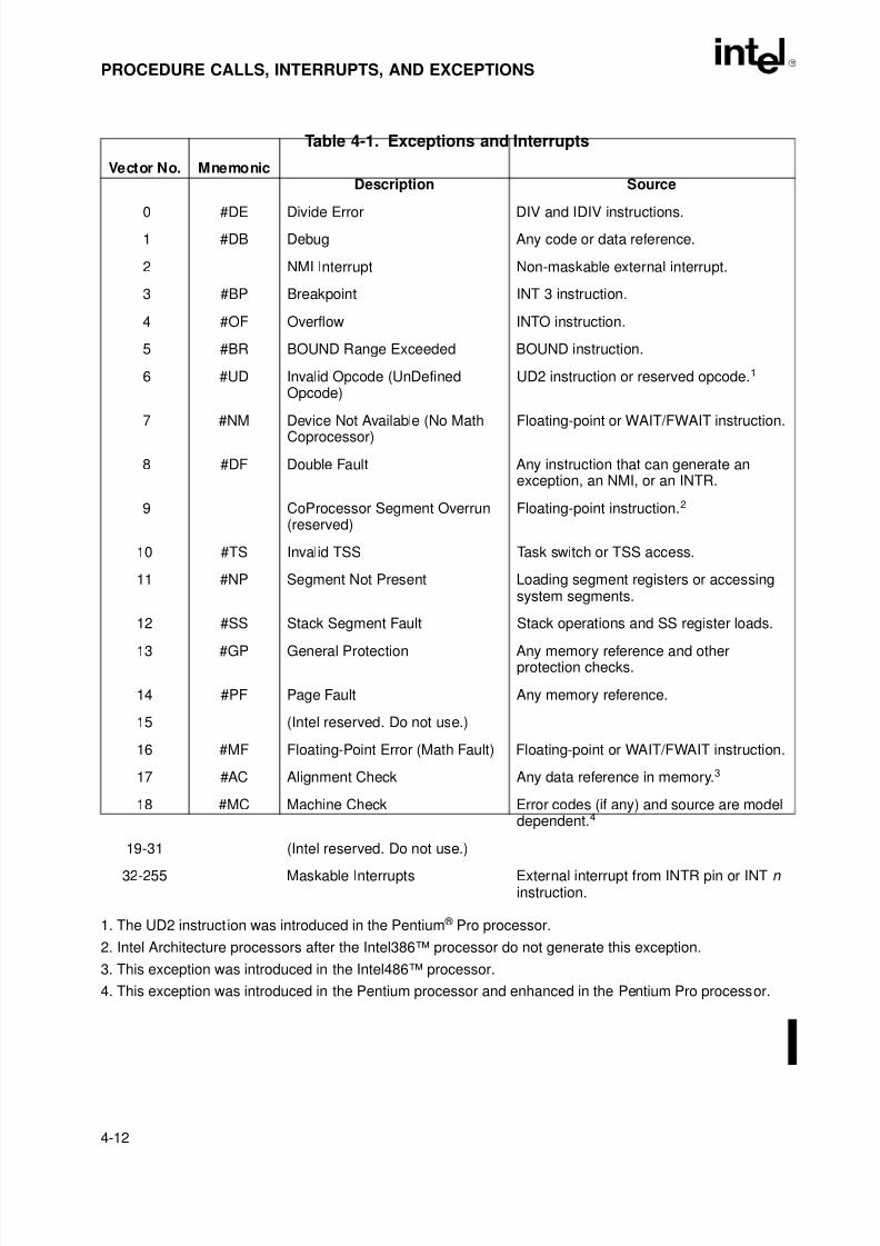
8/3/2019 Intel Architecture Software Developer's Manual, Volume 1: Basic Architecture
http://slidepdf.com/reader/full/intel-architecture-software-developers-manual-volume-1-basic-architecture 70/283
4-12
PROCEDURE CALLS, INTERRUPTS, AND EXCEPTIONS
1. The UD2 instruction was introduced in the Pentium ® Pro processor.
2. Intel Architecture processors after the Intel386™ processor do not generate this exception.
3. This exception was introduced in the Intel486™ processor.
4. This exception was introduced in the Pentium processor and enhanced in the Pentium Pro processor.
Table 4-1. Exceptions and Interrupts
Vector No. MnemonicDescription Source
0 #DE Divide Error DIV and IDIV instructions.
1 #DB Debug Any code or data reference.
2 NMI Interrupt Non-maskable external interrupt.
3 #BP Breakpoint INT 3 instruction.
4 #OF Overflow INTO instruction.
5 #BR BOUND Range Exceeded BOUND instruction.
6 #UD Invalid Opcode (UnDefinedOpcode)
UD2 instruction or reserved opcode.1
7 #NM Device Not Available (No MathCoprocessor) Floating-point or WAIT/FWAIT instruction.
8 #DF Double Fault Any instruction that can generate anexception, an NMI, or an INTR.
9 CoProcessor Segment Overrun(reserved)
Floating-point instruction.2
10 #TS Invalid TSS Task switch or TSS access.
11 #NP Segment Not Present Loading segment registers or accessingsystem segments.
12 #SS Stack Segment Fault Stack operations and SS register loads.
13 #GP General Protection Any memory reference and otherprotection checks.
14 #PF Page Fault Any memory reference.
15 (Intel reserved. Do not use.)
16 #MF Floating-Point Error (Math Fault) Floating-point or WAIT/FWAIT instruction.
17 #AC Alignment Check Any data reference in memory.3
18 #MC Machine Check Error codes (if any) and source are modeldependent.4
19-31 (Intel reserved. Do not use.)32-255 Maskable Interrupts External interrupt from INTR pin or INT n
instruction.
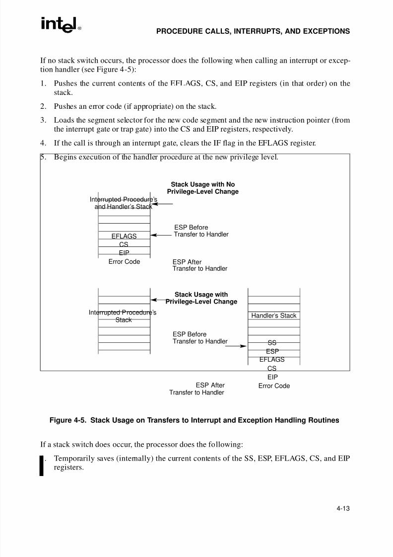
8/3/2019 Intel Architecture Software Developer's Manual, Volume 1: Basic Architecture
http://slidepdf.com/reader/full/intel-architecture-software-developers-manual-volume-1-basic-architecture 71/283
4-13
PROCEDURE CALLS, INTERRUPTS, AND EXCEPTIONS
If no stack switch occurs, the processor does the following when calling an interrupt or excep-tion handler (see Figure 4-5):
1. Pushes the current contents of the EFLAGS, CS, and EIP registers (in that order) on the
stack.2. Pushes an error code (if appropriate) on the stack.
3. Loads the segment selector for the new code segment and the new instruction pointer (fromthe interrupt gate or trap gate) into the CS and EIP registers, respectively.
4. If the call is through an interrupt gate, clears the IF flag in the EFLAGS register.
5. Begins execution of the handler procedure at the new privilege level.
If a stack switch does occur, the processor does the following:
1. Temporarily saves (internally) the current contents of the SS, ESP, EFLAGS, CS, and EIPregisters.
Figure 4-5. Stack Usage on Transfers to Interrupt and Exception Handling Routines
CS
Error Code
EFLAGS
CS
EIP
ESP AfterTransfer to Handler
Error Code
ESP BeforeTransfer to Handler
EFLAGS
EIP
SS
ESP
Stack Usage with No
Privilege-Level Change
Stack Usage withPrivilege-Level Change
Interrupted Procedure’s
Interrupted Procedure’sand Handler’s Stack
Handler’s Stack
ESP AfterTransfer to Handler
Transfer to HandlerESP Before
Stack
8/3/2019 Intel Architecture Software Developer's Manual, Volume 1: Basic Architecture
http://slidepdf.com/reader/full/intel-architecture-software-developers-manual-volume-1-basic-architecture 72/283
4-14
PROCEDURE CALLS, INTERRUPTS, AND EXCEPTIONS
2. Loads the segment selector and stack pointer for the new stack (that is, the stack for theprivilege level being called) from the TSS into the SS and ESP registers and switches to thenew stack.
3. Pushes the temporarily saved SS, ESP, EFLAGS, CS, and EIP values for the interruptedprocedure’s stack onto the new stack.
4. Pushes an error code on the new stack (if appropriate).
5. Loads the segment selector for the new code segment and the new instruction pointer (fromthe interrupt gate or trap gate) into the CS and EIP registers, respectively.
6. If the call is through an interrupt gate, clears the IF flag in the EFLAGS register.
7. Begins execution of the handler procedure at the new privilege level.
A return from an interrupt or exception handler is initiated with the IRET instruction. The IRET
instruction is similar to the far RET instruction, except that it also restores the contents of theEFLAGS register for the interrupted procedure:
When executing a return from an interrupt or exception handler from the same privilege level asthe interrupted procedure, the processor performs these actions:
1. Restores the CS and EIP registers to their values prior to the interrupt or exception.
2. Restores the EFLAGS register.
3. Increments the stack pointer appropriately
4. Resumes execution of the interrupted procedure.
When executing a return from an interrupt or exception handler from a different privilege levelthan the interrupted procedure, the processor performs these actions:
1. Performs a privilege check.
2. Restores the CS and EIP registers to their values prior to the interrupt or exception.
3. Restores the EFLAGS register.
4. Restores the SS and ESP registers to their values prior to the interrupt or exception,resulting in a stack switch back to the stack of the interrupted procedure.
5. Resumes execution of the interrupted procedure.
4.4.2. Calls to Interrupt or Exception Handler Tasks
Interrupt and exception handler routines can also be executed in a separate task. Here, an inter-rupt or exception causes a task switch to a handler task. The handler task is given its own addressspace and (optionally) can execute at a higher protection level than application programs ortasks.
The switch to the handler task is accomplished with an implicit task call that references a taskgate descriptor. The task gate provides access to the address space for the handler task. As part
8/3/2019 Intel Architecture Software Developer's Manual, Volume 1: Basic Architecture
http://slidepdf.com/reader/full/intel-architecture-software-developers-manual-volume-1-basic-architecture 73/283
4-15
PROCEDURE CALLS, INTERRUPTS, AND EXCEPTIONS
of the task switch, the processor saves complete state information for the interrupted program ortask. Upon returning from the handler task, the state of the interrupted program or task isrestored and execution continues. See Chapter 5, Interrupt and Exception Handling, in the Intel
Architecture Software Developer’s Manual, Volume 3, for a detailed description of the
processor’s mechanism for handling interrupts and exceptions through handler tasks.
4.4.3. Interrupt and Exception Handling in Real-Address Mode
When operating in real-address mode, the processor responds to an interrupt or exception withan implicit far call to an interrupt or exception handler. The processor uses the interrupt or excep-tion vector number as an index into an interrupt table. The interrupt table contains instructionpointers to the interrupt and exception handler procedures.
The processor saves the state of the EFLAGS register, the EIP register, the CS register, and an
optional error code on the stack before switching to the handler procedure.
A return from the interrupt or exception handler is carried out with the IRET instruction.
See Chapter 15, 8086 Emulation, in the Intel Architecture Software Developer’s Manual, Volume3, for more information on handling interrupts and exceptions in real-address mode.
4.4.4. INT n , INTO, INT 3, and BOUND Instructions
The INT n, INTO, INT 3, and BOUND instructions allow a program or task to explicitly call aninterrupt or exception handler. The INT n instruction uses an interrupt vector as an argument,which allows a program to call any interrupt handler.
The INTO instruction explicitly calls the overflow exception (#OF) handler if the overflow flag(OF) in the EFLAGS register is set. The OF flag indicates overflow on arithmetic instructions,but it does not automatically raise an overflow exception. An overflow exception can only beraised explicitly in either of the following ways:
• Execute the INTO instruction.
• Test the OF flag and execute the INT n instruction with an argument of 4 (the vectornumber of the overflow exception) if the flag is set.
Both the methods of dealing with overflow conditions allow a program to test for overflow atspecific places in the instruction stream.
The INT 3 instruction explicitly calls the breakpoint exception (#BP) handler.
The BOUND instruction explicitly calls the BOUND-range exceeded exception (#BR) handlerif an operand is found to be not within predefined boundaries in memory. This instruction isprovided for checking references to arrays and other data structures. Like the overflowexception, the BOUND-range exceeded exception can only be raised explicitly with theBOUND instruction or the INT n instruction with an argument of 5 (the vector number of thebounds-check exception). The processor does not implicitly perform bounds checks and raisethe BOUND-range exceeded exception.
8/3/2019 Intel Architecture Software Developer's Manual, Volume 1: Basic Architecture
http://slidepdf.com/reader/full/intel-architecture-software-developers-manual-volume-1-basic-architecture 74/283
4-16
PROCEDURE CALLS, INTERRUPTS, AND EXCEPTIONS
4.5. PROCEDURE CALLS FOR BLOCK-STRUCTUREDLANGUAGES
The Intel Architecture supports an alternate method of performing procedure calls with the
ENTER (enter procedure) and LEAVE (leave procedure) instructions. These instructions auto-matically create and release, respectively, stack frames for called procedures. The stack frameshave predefined spaces for local variables and the necessary pointers to allow coherent returnsfrom called procedures. They also allow scope rules to be implemented so that procedures canaccess their own local variables and some number of other variables located in other stack frames.
The ENTER and LEAVE instructions offer two benefits:
• They provide machine-language support for implementing block-structured languages,such as C and Pascal.
• They simplify procedure entry and exit in compiler-generated code.
4.5.1. ENTER Instruction
The ENTER instruction creates a stack frame compatible with the scope rules typically used inblock-structured languages. In block-structured languages, the scope of a procedure is the set of variables to which it has access. The rules for scope vary among languages. They may be basedon the nesting of procedures, the division of the program into separately compiled files, or someother modularization scheme.
The ENTER instruction has two operands. The first specifies the number of bytes to be reservedon the stack for dynamic storage for the procedure being called. Dynamic storage is the memoryallocated for variables created when the procedure is called, also known as automatic variables.The second parameter is the lexical nesting level (from 0 to 31) of the procedure. The nestinglevel is the depth of a procedure in a hierarchy of procedure calls. The lexical level is unrelatedto either the protection privilege level or to the I/O privilege level of the currently runningprogram or task.
The ENTER instruction in the following example, allocates 2K bytes of dynamic storage on thestack and sets up pointers to two previous stack frames in the stack frame for this procedure.
ENTER 2048,3
The lexical nesting level determines the number of stack frame pointers to copy into the newstack frame from the preceding frame. A stack frame pointer is a doubleword used to access thevariables of a procedure. The set of stack frame pointers used by a procedure to access thevariables of other procedures is called the display. The first doubleword in the display is a pointerto the previous stack frame. This pointer is used by a LEAVE instruction to undo the effect of anENTER instruction by discarding the current stack frame.
After the ENTER instruction creates the display for a procedure, it allocates the dynamic localvariables for the procedure by decrementing the contents of the ESP register by the number of bytes specified in the first parameter. This new value in the ESP register serves as the initial top-
of-stack for all PUSH and POP operations within the procedure.
8/3/2019 Intel Architecture Software Developer's Manual, Volume 1: Basic Architecture
http://slidepdf.com/reader/full/intel-architecture-software-developers-manual-volume-1-basic-architecture 75/283
4-17
PROCEDURE CALLS, INTERRUPTS, AND EXCEPTIONS
To allow a procedure to address its display, the ENTER instruction leaves the EBP registerpointing to the first doubleword in the display. Because stacks grow down, this is actually thedoubleword with the highest address in the display. Data manipulation instructions that specifythe EBP register as a base register automatically address locations within the stack segment
instead of the data segment.
The ENTER instruction can be used in two ways: nested and non-nested. If the lexical level is0, the non-nested form is used. The non-nested form pushes the contents of the EBP register onthe stack, copies the contents of the ESP register into the EBP register, and subtracts the firstoperand from the contents of the ESP register to allocate dynamic storage. The non-nested formdiffers from the nested form in that no stack frame pointers are copied. The nested form of theENTER instruction occurs when the second parameter (lexical level) is not zero.
The following pseudo code shows the formal definition of the ENTER instruction. STORAGEis the number of bytes of dynamic storage to allocate for local variables, and LEVEL is the
lexical nesting level.PUSH EBP;
FRAME_PTR ← ESP;
IF LEVEL > 0
THEN
DO (LEVEL − 1) times
EBP ← EBP − 4;
PUSH Pointer(EBP); (* doubleword pointed to by EBP *)
OD;
PUSH FRAME_PTR;
FI;
EBP ← FRAME_PTR;
ESP ← ESP − STORAGE;
The main procedure (in which all other procedures are nested) operates at the highest lexicallevel, level 1. The first procedure it calls operates at the next deeper lexical level, level 2. A level2 procedure can access the variables of the main program, which are at fixed locations specifiedby the compiler. In the case of level 1, the ENTER instruction allocates only the requesteddynamic storage on the stack because there is no previous display to copy.
A procedure which calls another procedure at a lower lexical level gives the called procedureaccess to the variables of the caller. The ENTER instruction provides this access by placing a
pointer to the calling procedure's stack frame in the display.A procedure which calls another procedure at the same lexical level should not give access to itsvariables. In this case, the ENTER instruction copies only that part of the display from thecalling procedure which refers to previously nested procedures operating at higher lexical levels.The new stack frame does not include the pointer for addressing the calling procedure’s stack frame.
The ENTER instruction treats a re-entrant procedure as a call to a procedure at the same lexicallevel. In this case, each succeeding iteration of the re-entrant procedure can address only its ownvariables and the variables of the procedures within which it is nested. A re-entrant procedurealways can address its own variables; it does not require pointers to the stack frames of previous
iterations.
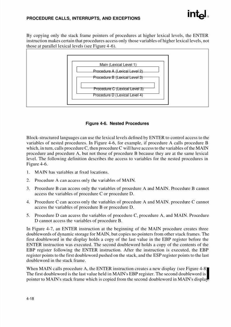
8/3/2019 Intel Architecture Software Developer's Manual, Volume 1: Basic Architecture
http://slidepdf.com/reader/full/intel-architecture-software-developers-manual-volume-1-basic-architecture 76/283
4-18
PROCEDURE CALLS, INTERRUPTS, AND EXCEPTIONS
By copying only the stack frame pointers of procedures at higher lexical levels, the ENTERinstruction makes certain that procedures access only those variables of higher lexical levels, notthose at parallel lexical levels (see Figure 4-6).
Block-structured languages can use the lexical levels defined by ENTER to control access to thevariables of nested procedures. In Figure 4-6, for example, if procedure A calls procedure Bwhich, in turn, calls procedure C, then procedure C will have access to the variables of the MAINprocedure and procedure A, but not those of procedure B because they are at the same lexicallevel. The following definition describes the access to variables for the nested procedures inFigure 4-6.
1. MAIN has variables at fixed locations.
2. Procedure A can access only the variables of MAIN.
3. Procedure B can access only the variables of procedure A and MAIN. Procedure B cannotaccess the variables of procedure C or procedure D.
4. Procedure C can access only the variables of procedure A and MAIN. procedure C cannotaccess the variables of procedure B or procedure D.
5. Procedure D can access the variables of procedure C, procedure A, and MAIN. ProcedureD cannot access the variables of procedure B.
In Figure 4-7, an ENTER instruction at the beginning of the MAIN procedure creates threedoublewords of dynamic storage for MAIN, but copies no pointers from other stack frames. Thefirst doubleword in the display holds a copy of the last value in the EBP register before theENTER instruction was executed. The second doubleword holds a copy of the contents of theEBP register following the ENTER instruction. After the instruction is executed, the EBPregister points to the first doubleword pushed on the stack, and the ESP register points to the lastdoubleword in the stack frame.
When MAIN calls procedure A, the ENTER instruction creates a new display (see Figure 4-8).The first doubleword is the last value held in MAIN's EBP register. The second doubleword is a
pointer to MAIN's stack frame which is copied from the second doubleword in MAIN's display.
Figure 4-6. Nested Procedures
Main (Lexical Level 1)
Procedure A (Lexical Level 2)
Procedure B (Lexical Level 3)
Procedure C (Lexical Level 3)
Procedure D (Lexical Level 4)
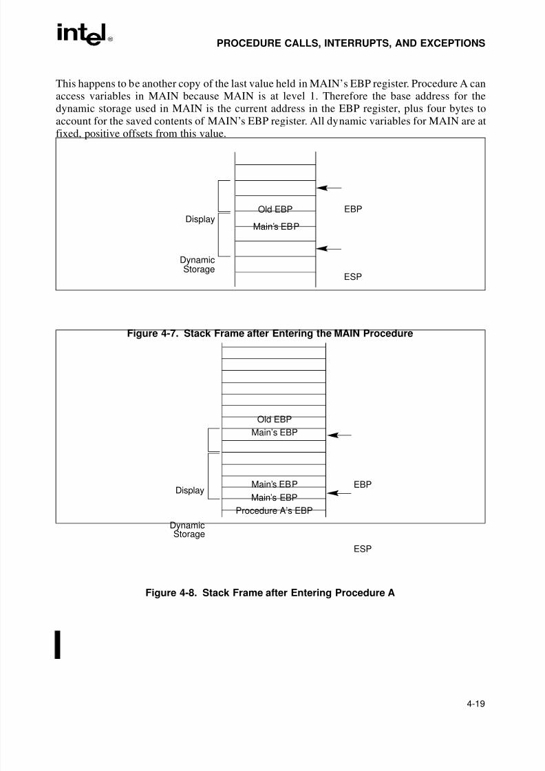
8/3/2019 Intel Architecture Software Developer's Manual, Volume 1: Basic Architecture
http://slidepdf.com/reader/full/intel-architecture-software-developers-manual-volume-1-basic-architecture 77/283
4-19
PROCEDURE CALLS, INTERRUPTS, AND EXCEPTIONS
This happens to be another copy of the last value held in MAIN’s EBP register. Procedure A canaccess variables in MAIN because MAIN is at level 1. Therefore the base address for thedynamic storage used in MAIN is the current address in the EBP register, plus four bytes toaccount for the saved contents of MAIN’s EBP register. All dynamic variables for MAIN are at
fixed, positive offsets from this value.
Figure 4-7. Stack Frame after Entering the MAIN Procedure
Figure 4-8. Stack Frame after Entering Procedure A
EBPDisplay
Old EBP
ESP
Main’s EBP
DynamicStorage
EBPDisplay
Old EBP
ESP
Main’s EBP
DynamicStorage
Procedure A’s EBP
Main’s EBP
Main’s EBP
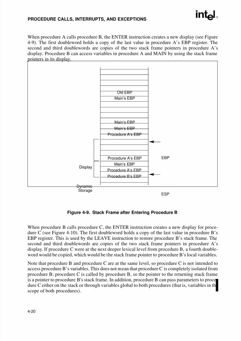
8/3/2019 Intel Architecture Software Developer's Manual, Volume 1: Basic Architecture
http://slidepdf.com/reader/full/intel-architecture-software-developers-manual-volume-1-basic-architecture 78/283
4-20
PROCEDURE CALLS, INTERRUPTS, AND EXCEPTIONS
When procedure A calls procedure B, the ENTER instruction creates a new display (see Figure4-9). The first doubleword holds a copy of the last value in procedure A’s EBP register. Thesecond and third doublewords are copies of the two stack frame pointers in procedure A’sdisplay. Procedure B can access variables in procedure A and MAIN by using the stack frame
pointers in its display.
When procedure B calls procedure C, the ENTER instruction creates a new display for proce-
dure C (see Figure 4-10). The first doubleword holds a copy of the last value in procedure B’sEBP register. This is used by the LEAVE instruction to restore procedure B’s stack frame. Thesecond and third doublewords are copies of the two stack frame pointers in procedure A’sdisplay. If procedure C were at the next deeper lexical level from procedure B, a fourth double-word would be copied, which would be the stack frame pointer to procedure B’s local variables.
Note that procedure B and procedure C are at the same level, so procedure C is not intended toaccess procedure B’s variables. This does not mean that procedure C is completely isolated fromprocedure B; procedure C is called by procedure B, so the pointer to the returning stack frameis a pointer to procedure B's stack frame. In addition, procedure B can pass parameters to proce-dure C either on the stack or through variables global to both procedures (that is, variables in the
scope of both procedures).
Figure 4-9. Stack Frame after Entering Procedure B
EBP
Display
Old EBP
ESP
Main’s EBP
DynamicStorage
Procedure A’s EBP
Main’s EBP
Main’s EBP
Procedure A’s EBP
Procedure B’s EBP
Main’s EBP
Procedure A’s EBP
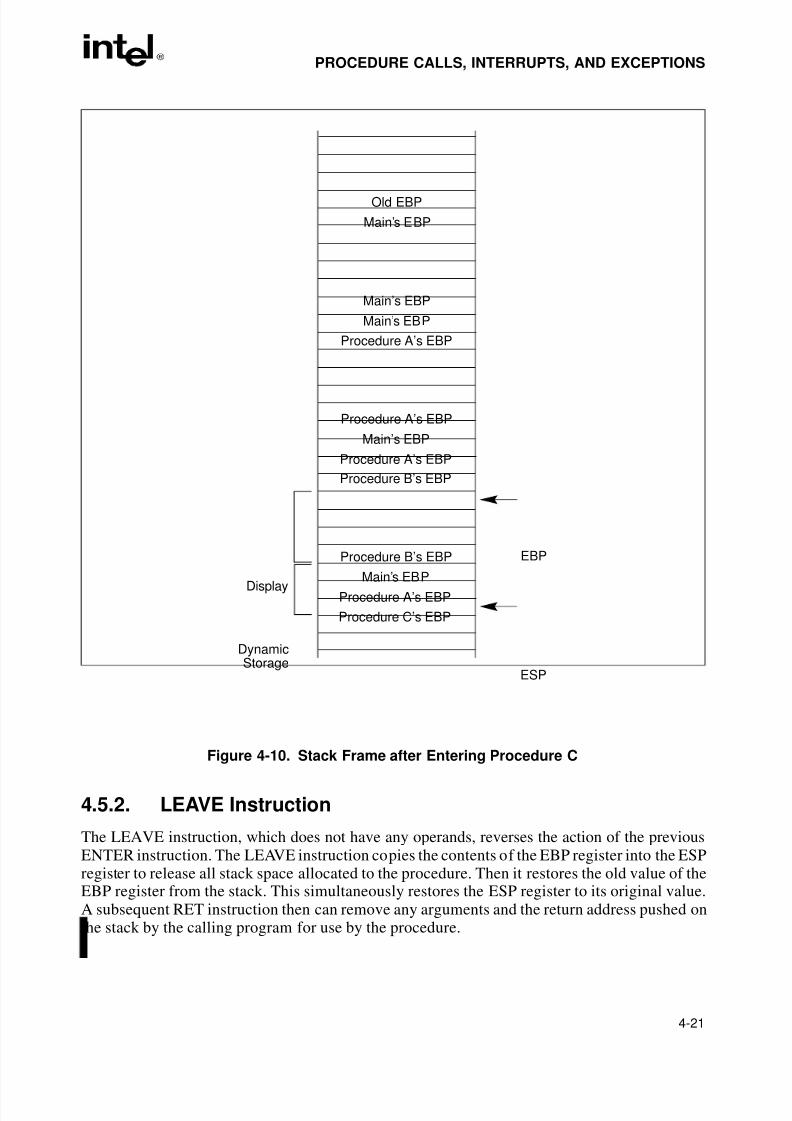
8/3/2019 Intel Architecture Software Developer's Manual, Volume 1: Basic Architecture
http://slidepdf.com/reader/full/intel-architecture-software-developers-manual-volume-1-basic-architecture 79/283
4-21
PROCEDURE CALLS, INTERRUPTS, AND EXCEPTIONS
4.5.2. LEAVE Instruction
The LEAVE instruction, which does not have any operands, reverses the action of the previousENTER instruction. The LEAVE instruction copies the contents of the EBP register into the ESPregister to release all stack space allocated to the procedure. Then it restores the old value of theEBP register from the stack. This simultaneously restores the ESP register to its original value.A subsequent RET instruction then can remove any arguments and the return address pushed onthe stack by the calling program for use by the procedure.
Figure 4-10. Stack Frame after Entering Procedure C
EBP
Display
Old EBP
ESP
Main’s EBP
DynamicStorage
Procedure A’s EBP
Main’s EBP
Main’s EBP
Procedure A’s EBP
Procedure B’s EBP
Main’s EBP
Procedure A’s EBP
Procedure B’s EBP
Procedure C’s EBP
Main’s EBPProcedure A’s EBP

8/3/2019 Intel Architecture Software Developer's Manual, Volume 1: Basic Architecture
http://slidepdf.com/reader/full/intel-architecture-software-developers-manual-volume-1-basic-architecture 80/283
8/3/2019 Intel Architecture Software Developer's Manual, Volume 1: Basic Architecture
http://slidepdf.com/reader/full/intel-architecture-software-developers-manual-volume-1-basic-architecture 81/283
5Data Types andAddressing Modes

8/3/2019 Intel Architecture Software Developer's Manual, Volume 1: Basic Architecture
http://slidepdf.com/reader/full/intel-architecture-software-developers-manual-volume-1-basic-architecture 82/283
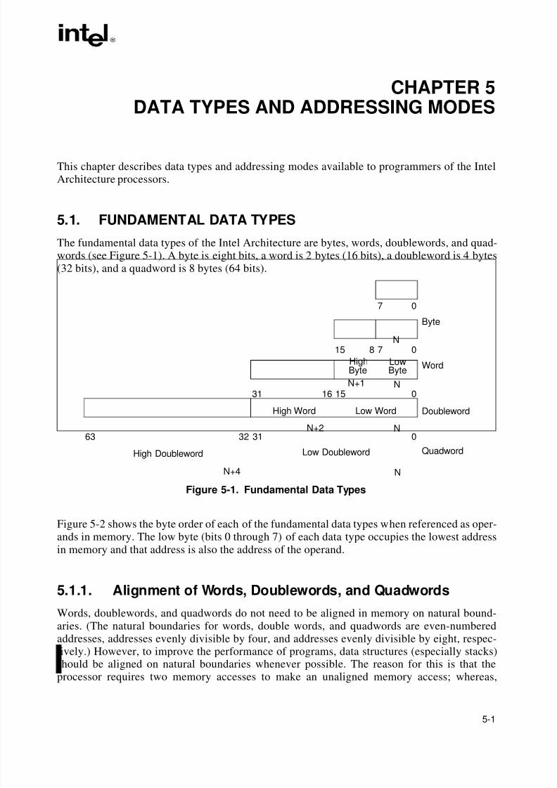
8/3/2019 Intel Architecture Software Developer's Manual, Volume 1: Basic Architecture
http://slidepdf.com/reader/full/intel-architecture-software-developers-manual-volume-1-basic-architecture 83/283
5-1
CHAPTER 5DATA TYPES AND ADDRESSING MODES
This chapter describes data types and addressing modes available to programmers of the IntelArchitecture processors.
5.1. FUNDAMENTAL DATA TYPES
The fundamental data types of the Intel Architecture are bytes, words, doublewords, and quad-words (see Figure 5-1). A byte is eight bits, a word is 2 bytes (16 bits), a doubleword is 4 bytes
(32 bits), and a quadword is 8 bytes (64 bits).
Figure 5-2 shows the byte order of each of the fundamental data types when referenced as oper-
ands in memory. The low byte (bits 0 through 7) of each data type occupies the lowest addressin memory and that address is also the address of the operand.
5.1.1. Alignment of Words, Doublewords, and Quadwords
Words, doublewords, and quadwords do not need to be aligned in memory on natural bound-aries. (The natural boundaries for words, double words, and quadwords are even-numberedaddresses, addresses evenly divisible by four, and addresses evenly divisible by eight, respec-tively.) However, to improve the performance of programs, data structures (especially stacks)should be aligned on natural boundaries whenever possible. The reason for this is that the
processor requires two memory accesses to make an unaligned memory access; whereas,
Figure 5-1. Fundamental Data Types
0
63
Quadword
0
Word
31
0
Doubleword
15
0
Byte
7
78N
Low WordHigh Word
Low DoublewordHigh Doubleword
1516
3132
N+1 N
N
N+2
N+4
N
LowByte
HighByte
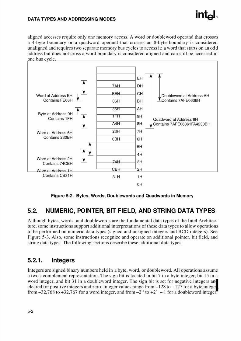
8/3/2019 Intel Architecture Software Developer's Manual, Volume 1: Basic Architecture
http://slidepdf.com/reader/full/intel-architecture-software-developers-manual-volume-1-basic-architecture 84/283
5-2
DATA TYPES AND ADDRESSING MODES
aligned accesses require only one memory access. A word or doubleword operand that crossesa 4-byte boundary or a quadword operand that crosses an 8-byte boundary is consideredunaligned and requires two separate memory bus cycles to access it; a word that starts on an oddaddress but does not cross a word boundary is considered aligned and can still be accessed in
one bus cycle.
5.2. NUMERIC, POINTER, BIT FIELD, AND STRING DATA TYPES
Although bytes, words, and doublewords are the fundamental data types of the Intel Architec-ture, some instructions support additional interpretations of these data types to allow operations
to be performed on numeric data types (signed and unsigned integers and BCD integers). SeeFigure 5-3. Also, some instructions recognize and operate on additional pointer, bit field, andstring data types. The following sections describe these additional data types.
5.2.1. Integers
Integers are signed binary numbers held in a byte, word, or doubleword. All operations assumea two's complement representation. The sign bit is located in bit 7 in a byte integer, bit 15 in aword integer, and bit 31 in a doubleword integer. The sign bit is set for negative integers andcleared for positive integers and zero. Integer values range from –128 to +127 for a byte integer,
from –32,768 to +32,767 for a word integer, and from –231 to +231 – 1 for a doubleword integer.
Figure 5-2. Bytes, Words, Doublewords and Quadwords in Memory
EH
DH7AH
CHFEH
BH06H
AH36H
9H1FH
8HA4H
7H23H
6H0BH
5H
4H
3H74H
2HCBH
1H31H
0H
Quadword at Address 6HContains 7AFE06361FA4230BH
Doubleword at Address AHContains 7AFE0636H
Word at Address BHContains FE06H
Byte at Address 9HContains 1FH
Word at Address 6HContains 230BH
Word at Address 1H
Contains CB31H
Word at Address 2HContains 74CBH
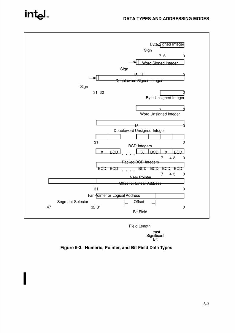
8/3/2019 Intel Architecture Software Developer's Manual, Volume 1: Basic Architecture
http://slidepdf.com/reader/full/intel-architecture-software-developers-manual-volume-1-basic-architecture 85/283
5-3
DATA TYPES AND ADDRESSING MODES
Figure 5-3. Numeric, Pointer, and Bit Field Data Types
047
Far Pointer or Logical Address
Segment Selector
32 31
Offset
0
Near Pointer
31
Offset or Linear Address
Bit Field
Field Length
0
Doubleword Unsigned Integer
31
0
Packed BCD Integers
7
BCDBCDBCDBCDBCDBCD
34. . . .
0
BCD Integers
7
BCDXBCDXBCDX
34. . . .
0
Word Unsigned Integer
15
0
Byte Unsigned Integer
7
0
Doubleword Signed Integer
31 30
0
Word Signed Integer
15 14
0
Byte Signed Integer
7 6
Sign
Sign
Sign
Least
BitSignificant
8/3/2019 Intel Architecture Software Developer's Manual, Volume 1: Basic Architecture
http://slidepdf.com/reader/full/intel-architecture-software-developers-manual-volume-1-basic-architecture 86/283
5-4
DATA TYPES AND ADDRESSING MODES
5.2.2. Unsigned Integers
Unsigned integers are unsigned binary numbers contained in a byte, word, or doubleword.Unsigned integer values range from 0 to 255 for an unsigned byte integer, from 0 to 65,535 for
an unsigned word integer, and from 0 to 232 – 1 for an unsigned doubleword integer. Unsignedintegers are sometimes referred to as ordinals.
5.2.3. BCD Integers
Binary-coded decimal integers (BCD integers) are unsigned 4-bit integers with valid valuesranging from 0 to 9. BCD integers can be unpacked (one BCD digit per byte) or packed (twoBCD digits per byte). The value of an unpacked BCD integer is the binary value of the low half-byte (bits 0 through 3). The high half-byte (bits 4 through 7) can be any value during additionand subtraction, but must be zero during multiplication and division.
Packed BCD integers allow two BCD digits to be contained in one byte. Here, the digit in thehigh half-byte is more significant than the digit in the low half-byte.
5.2.4. Pointers
Pointers are addresses of locations in memory. The Pentium Pro processor recognizes two typesof pointers: a near pointer (32 bits) and a far pointer (48 bits). A near pointer is a 32-bit offset(also called an effective address) within a segment. Near pointers are used for all memory refer-ences in a flat memory model or for references in a segmented model where the identity of the
segment being accessed is implied. A far pointer is a 48-bit logical address, consisting of a 16-bitsegment selector and a 32-bit offset. Far pointers are used for memory references in a segmentedmemory model where the identity of a segment being accessed must be specified explicitly.
5.2.5. Bit Fields
A bit field is a contiguous sequence of bits. It can begin at any bit position of any byte in memoryand can contain up to 32 bits.
5.2.6. Strings
Strings are continuous sequences of bits, bytes, words, or doublewords. A bit string can beginat any bit position of any byte and can contain up to 232 – 1 bits. A byte string can contain bytes,words, or doublewords and can range from zero to 232 – 1 bytes (4 gigabytes).
8/3/2019 Intel Architecture Software Developer's Manual, Volume 1: Basic Architecture
http://slidepdf.com/reader/full/intel-architecture-software-developers-manual-volume-1-basic-architecture 87/283
5-5
DATA TYPES AND ADDRESSING MODES
5.2.7. Floating-Point Data Types
The processor’s floating-point instructions recognize a set of real, integer, and BCD integer datatypes. See Section 7.4., “Floating-Point Data Types and Formats”, for a description of FPU data
types.
5.2.8. MMX™ Technology Data Types
Intel Architecture processors that implement the Intel MMX technology recognize a set of packed 64-bit data types. See Section 8.1.2., “MMX™ Data Types”, for a description of theMMX data types.
5.3. OPERAND ADDRESSINGAn Intel Architecture machine-instruction acts on zero or more operands. Some operands arespecified explicitly in an instruction and others are implicit to an instruction. An operand can belocated in any of the following places:
• The instruction itself (an immediate operand).
• A register.
• A memory location.
• An I/O port.
5.3.1. Immediate Operands
Some instructions use data encoded in the instruction itself as a source operand. These operandsare called immediate operands (or simply immediates). For example, the following ADDinstruction adds an immediate value of 14 to the contents of the EAX register:
ADD EAX, 14
All the arithmetic instructions (except the DIV and IDIV instructions) allow the source operandto be an immediate value. The maximum value allowed for an immediate operand varies amonginstructions, but can never be greater than the maximum value of an unsigned doublewordinteger (232).
5.3.2. Register Operands
Source and destination operands can be located in any of the following registers, depending onthe instruction being executed:
• The 32-bit general-purpose registers (EAX, EBX, ECX, EDX, ESI, EDI, ESP, or EBP).
• The 16-bit general-purpose registers (AX, BX, CX, DX, SI, DI, SP, or BP).
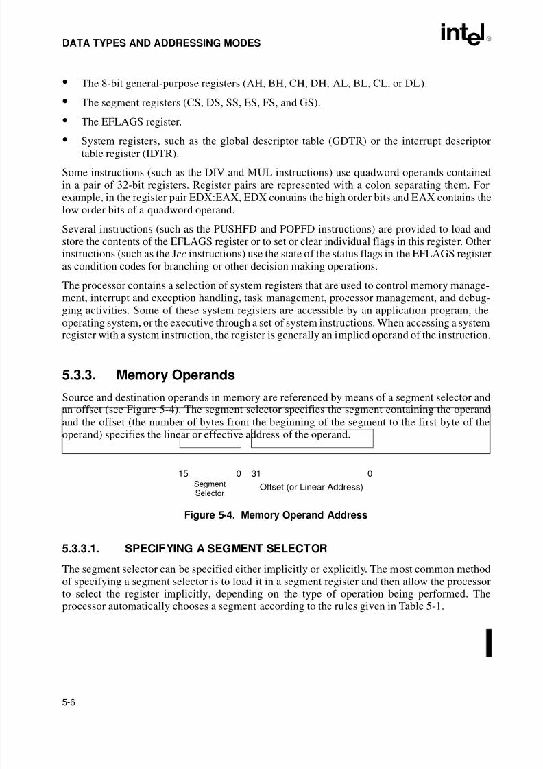
8/3/2019 Intel Architecture Software Developer's Manual, Volume 1: Basic Architecture
http://slidepdf.com/reader/full/intel-architecture-software-developers-manual-volume-1-basic-architecture 88/283
5-6
DATA TYPES AND ADDRESSING MODES
• The 8-bit general-purpose registers (AH, BH, CH, DH, AL, BL, CL, or DL).
• The segment registers (CS, DS, SS, ES, FS, and GS).
• The EFLAGS register.
• System registers, such as the global descriptor table (GDTR) or the interrupt descriptortable register (IDTR).
Some instructions (such as the DIV and MUL instructions) use quadword operands containedin a pair of 32-bit registers. Register pairs are represented with a colon separating them. Forexample, in the register pair EDX:EAX, EDX contains the high order bits and EAX contains thelow order bits of a quadword operand.
Several instructions (such as the PUSHFD and POPFD instructions) are provided to load andstore the contents of the EFLAGS register or to set or clear individual flags in this register. Otherinstructions (such as the Jcc instructions) use the state of the status flags in the EFLAGS register
as condition codes for branching or other decision making operations.
The processor contains a selection of system registers that are used to control memory manage-ment, interrupt and exception handling, task management, processor management, and debug-ging activities. Some of these system registers are accessible by an application program, theoperating system, or the executive through a set of system instructions. When accessing a systemregister with a system instruction, the register is generally an implied operand of the instruction.
5.3.3. Memory Operands
Source and destination operands in memory are referenced by means of a segment selector andan offset (see Figure 5-4). The segment selector specifies the segment containing the operandand the offset (the number of bytes from the beginning of the segment to the first byte of theoperand) specifies the linear or effective address of the operand.
5.3.3.1. SPECIFYING A SEGMENT SELECTOR
The segment selector can be specified either implicitly or explicitly. The most common methodof specifying a segment selector is to load it in a segment register and then allow the processorto select the register implicitly, depending on the type of operation being performed. Theprocessor automatically chooses a segment according to the rules given in Table 5-1.
Figure 5-4. Memory Operand Address
Offset (or Linear Address)
015Segment
310
Selector
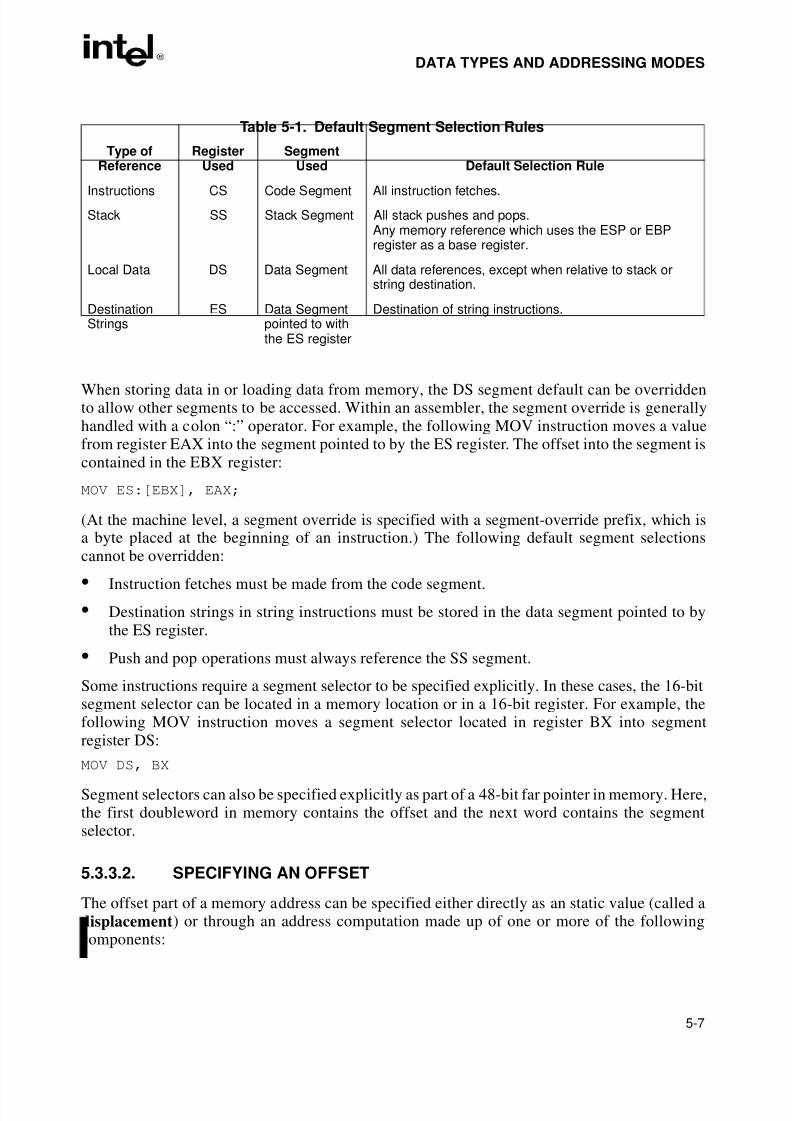
8/3/2019 Intel Architecture Software Developer's Manual, Volume 1: Basic Architecture
http://slidepdf.com/reader/full/intel-architecture-software-developers-manual-volume-1-basic-architecture 89/283
5-7
DATA TYPES AND ADDRESSING MODES
When storing data in or loading data from memory, the DS segment default can be overriddento allow other segments to be accessed. Within an assembler, the segment override is generallyhandled with a colon “:” operator. For example, the following MOV instruction moves a valuefrom register EAX into the segment pointed to by the ES register. The offset into the segment iscontained in the EBX register:
MOV ES:[EBX], EAX;
(At the machine level, a segment override is specified with a segment-override prefix, which isa byte placed at the beginning of an instruction.) The following default segment selectionscannot be overridden:
• Instruction fetches must be made from the code segment.
• Destination strings in string instructions must be stored in the data segment pointed to bythe ES register.
• Push and pop operations must always reference the SS segment.
Some instructions require a segment selector to be specified explicitly. In these cases, the 16-bitsegment selector can be located in a memory location or in a 16-bit register. For example, thefollowing MOV instruction moves a segment selector located in register BX into segmentregister DS:
MOV DS, BX
Segment selectors can also be specified explicitly as part of a 48-bit far pointer in memory. Here,the first doubleword in memory contains the offset and the next word contains the segmentselector.
5.3.3.2. SPECIFYING AN OFFSET
The offset part of a memory address can be specified either directly as an static value (called a
displacement) or through an address computation made up of one or more of the followingcomponents:
Table 5-1. Default Segment Selection Rules
Type ofReference
RegisterUsed
SegmentUsed Default Selection Rule
Instructions CS Code Segment All instruction fetches.
Stack SS Stack Segment All stack pushes and pops.Any memory reference which uses the ESP or EBPregister as a base register.
Local Data DS Data Segment All data references, except when relative to stack orstring destination.
DestinationStrings
ES Data Segmentpointed to withthe ES register
Destination of string instructions.
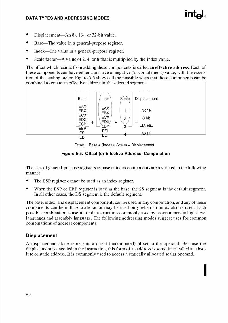
8/3/2019 Intel Architecture Software Developer's Manual, Volume 1: Basic Architecture
http://slidepdf.com/reader/full/intel-architecture-software-developers-manual-volume-1-basic-architecture 90/283
5-8
DATA TYPES AND ADDRESSING MODES
• Displacement—An 8-, 16-, or 32-bit value.
• Base—The value in a general-purpose register.
• Index—The value in a general-purpose register.
• Scale factor—A value of 2, 4, or 8 that is multiplied by the index value.
The offset which results from adding these components is called an effective address. Each of these components can have either a positive or negative (2s complement) value, with the excep-tion of the scaling factor. Figure 5-5 shows all the possible ways that these components can becombined to create an effective address in the selected segment.
The uses of general-purpose registers as base or index components are restricted in the followingmanner:
• The ESP register cannot be used as an index register.
• When the ESP or EBP register is used as the base, the SS segment is the default segment.In all other cases, the DS segment is the default segment.
The base, index, and displacement components can be used in any combination, and any of thesecomponents can be null. A scale factor may be used only when an index also is used. Eachpossible combination is useful for data structures commonly used by programmers in high-levellanguages and assembly language. The following addressing modes suggest uses for common
combinations of address components.
Displacement
A displacement alone represents a direct (uncomputed) offset to the operand. Because thedisplacement is encoded in the instruction, this form of an address is sometimes called an abso-lute or static address. It is commonly used to access a statically allocated scalar operand.
Figure 5-5. Offset (or Effective Address) Computation
Offset = Base + (Index ∗ Scale) + Displacement
Base
EAX
EBXECXEDXESPEBPESIEDI
EAXEBXECXEDX
EBPESIEDI
1 None
2
3
4
8-bit
16-bit
32-bit
Index Scale Displacement
*+ +
8/3/2019 Intel Architecture Software Developer's Manual, Volume 1: Basic Architecture
http://slidepdf.com/reader/full/intel-architecture-software-developers-manual-volume-1-basic-architecture 91/283
5-9
DATA TYPES AND ADDRESSING MODES
Base
A base alone represents an indirect offset to the operand. Since the value in the base register canchange, it can be used for dynamic storage of variables and data structures.
Base + Displacement
A base register and a displacement can be used together for two distinct purposes:
• As an index into an array when the element size is not 2, 4, or 8 bytes—The displacementcomponent encodes the static offset to the beginning of the array. The base register holdsthe results of a calculation to determine the offset to a specific element within the array.
• To access a field of a record—The base register holds the address of the beginning of therecord, while the displacement is an static offset to the field.
An important special case of this combination is access to parameters in a procedure activationrecord. A procedure activation record is the stack frame created when a procedure is entered.Here, the EBP register is the best choice for the base register, because it automatically selectsthe stack segment. This is a compact encoding for this common function.
(Index ∗ Scale) + Displacement
This address mode offers an efficient way to index into a static array when the element size is 2,4, or 8 bytes. The displacement locates the beginning of the array, the index register holds thesubscript of the desired array element, and the processor automatically converts the subscriptinto an index by applying the scaling factor.
Base + Index + Displacement
Using two registers together supports either a two-dimensional array (the displacement holds theaddress of the beginning of the array) or one of several instances of an array of records (thedisplacement is an offset to a field within the record).
Base + (Index ∗ Scale) + Displacement
Using all the addressing components together allows efficient indexing of a two-dimensionalarray when the elements of the array are 2, 4, or 8 bytes in size.
5.3.3.3. ASSEMBLER AND COMPILER ADDRESSING MODES
At the machine-code level, the selected combination of displacement, base register, indexregister, and scale factor is encoded in an instruction. All assemblers permit a programmer to useany of the allowable combinations of these addressing components to address operands. High-level language (HLL) compilers will select an appropriate combination of these componentsbased on the HHL construct a programmer defines.
8/3/2019 Intel Architecture Software Developer's Manual, Volume 1: Basic Architecture
http://slidepdf.com/reader/full/intel-architecture-software-developers-manual-volume-1-basic-architecture 92/283
5-10
DATA TYPES AND ADDRESSING MODES
5.3.4. I/O Port Addressing
The processor supports an I/O address space that contains up to 65,536 8-bit I/O ports. Ports thatare 16-bit and 32-bit may also be defined in the I/O address space. An I/O port can be addressed
with either an immediate operand or a value in the DX register. See Chapter 9, Input/Output , formore information about I/O port addressing.
8/3/2019 Intel Architecture Software Developer's Manual, Volume 1: Basic Architecture
http://slidepdf.com/reader/full/intel-architecture-software-developers-manual-volume-1-basic-architecture 93/283
6Instruction SetSummary

8/3/2019 Intel Architecture Software Developer's Manual, Volume 1: Basic Architecture
http://slidepdf.com/reader/full/intel-architecture-software-developers-manual-volume-1-basic-architecture 94/283
8/3/2019 Intel Architecture Software Developer's Manual, Volume 1: Basic Architecture
http://slidepdf.com/reader/full/intel-architecture-software-developers-manual-volume-1-basic-architecture 95/283
6-1
CHAPTER 6INSTRUCTION SET SUMMARY
This chapter lists all the instructions in the Intel Architecture instruction set, divided into threefunctional groups: integer, floating-point, and system. It also briefly describes each of the integerinstructions.
Brief descriptions of the floating-point instructions are given in Chapter 7, Floating-Point Unit ;brief descriptions of the system instructions are given in the Intel Architecture Software Devel-
oper’s Manual, Volume 3.
Detailed descriptions of all the Intel Architecture instructions are given in Intel Architecture
Software Developer’s Manual, Volume 2. Included in this volume are a description of eachinstruction’s encoding and operation, the effect of an instruction on the EFLAGS flags, and theexceptions an instruction may generate.
6.1. NEW INTEL ARCHITECTURE INSTRUCTIONS
The following sections give the Intel Architecture instructions that were new in the MMX Tech-nology and in the Pentium Pro, Pentium, and Intel486 processors.
6.1.1. New Instructions Introduced with the MMX™ Technology
The Intel MMX technology introduced a new set of instructions to the Intel Architecture,designed to enhance the performance of multimedia applications. These instructions are recog-nized by all Intel Architecture processors that implement the MMX technology. The MMXinstructions are listed in Section 6.2.2., “MMX™ Technology Instructions”.
6.1.2. New Instructions in the Pentium ® Pro Processor
The following instructions are new in the Pentium Pro processor:• CMOVcc—Conditional move (see Section 6.3.1.2., “Conditional Move Instructions”).
• FCMOVcc—Floating-point conditional move on condition-code flags in EFLAGS register(see Section 7.5.3., “Data Transfer Instructions”).
• FCOMI/FCOMIP/FUCOMI/FUCOMIP—Floating-point compare and set condition-codeflags in EFLAGS register (see Section 7.5.6., “Comparison and Classification Instruc-tions”).
• RDPMC—Read performance monitoring counters (see “RDPMC—Read Performance-Monitoring Counters” in Chapter 3 of the Intel Architecture Software Developer’s Manual,
8/3/2019 Intel Architecture Software Developer's Manual, Volume 1: Basic Architecture
http://slidepdf.com/reader/full/intel-architecture-software-developers-manual-volume-1-basic-architecture 96/283
8/3/2019 Intel Architecture Software Developer's Manual, Volume 1: Basic Architecture
http://slidepdf.com/reader/full/intel-architecture-software-developers-manual-volume-1-basic-architecture 97/283
6-3
INSTRUCTION SET SUMMARY
6.2.1. Integer Instructions
Integer instructions perform the integer arithmetic, logic, and program flow control operationsthat programmers commonly use to write application and system software to run on an Intel
Architecture processor. In the following sections, the integer instructions are divided into severalinstruction subgroups.
6.2.1.1. DATA TRANSFER INSTRUCTIONS
MOV Move
CMOVE/CMOVZ Conditional move if equal/Conditional move if zero
CMOVNE/CMOVNZ Conditional move if not equal/Conditional move if not zero
CMOVA/CMOVNBE Conditional move if above/Conditional move if not below
or equal
CMOVAE/CMOVNB Conditional move if above or equal/Conditional move if not below
CMOVB/CMOVNAE Conditional move if below/Conditional move if not aboveor equal
CMOVBE/CMOVNA Conditional move if below or equal/Conditional move if not above
CMOVG/CMOVNLE Conditional move if greater/Conditional move if not less
or equalCMOVGE/CMOVNL Conditional move if greater or equal/Conditional move if
not less
CMOVL/CMOVNGE Conditional move if less/Conditional move if not greateror equal
CMOVLE/CMOVNG Conditional move if less or equal/Conditional move if not greater
CMOVC Conditional move if carry
CMOVNC Conditional move if not carry
CMOVO Conditional move if overflow
CMOVNO Conditional move if not overflow
CMOVS Conditional move if sign (negative)
CMOVNS Conditional move if not sign (non-negative)
CMOVP/CMOVPE Conditional move if parity/Conditional move if parity even
CMOVNP/CMOVPO Conditional move if not parity/Conditional move if parity odd
XCHG Exchange
8/3/2019 Intel Architecture Software Developer's Manual, Volume 1: Basic Architecture
http://slidepdf.com/reader/full/intel-architecture-software-developers-manual-volume-1-basic-architecture 98/283
6-4
INSTRUCTION SET SUMMARY
BSWAP Byte swap
XADD Exchange and add
CMPXCHG Compare and exchange
CMPXCHG8B Compare and exchange 8 bytes
PUSH Push onto stack
POP Pop off of stack
PUSHA/PUSHAD Push general-purpose registers onto stack
POPA/POPAD Pop general-purpose registers from stack
IN Read from a port
OUT Write to a port
CWD/CDQ Convert word to doubleword/Convert doubleword to quadword
CBW/CWDE Convert byte to word/Convert word to doubleword in EAX register
MOVSX Move and sign extend
MOVZX Move and zero extend
6.2.1.2. BINARY ARITHMETIC INSTRUCTIONS
ADD Integer add
ADC Add with carry
SUB Subtract
SBB Subtract with borrow
IMUL Signed multiply
MUL Unsigned multiply
IDIV Signed divide
DIV Unsigned divide
INC Increment
DEC Decrement
NEG Negate
CMP Compare
6.2.1.3. DECIMAL ARITHMETIC
DAA Decimal adjust after addition
DAS Decimal adjust after subtraction
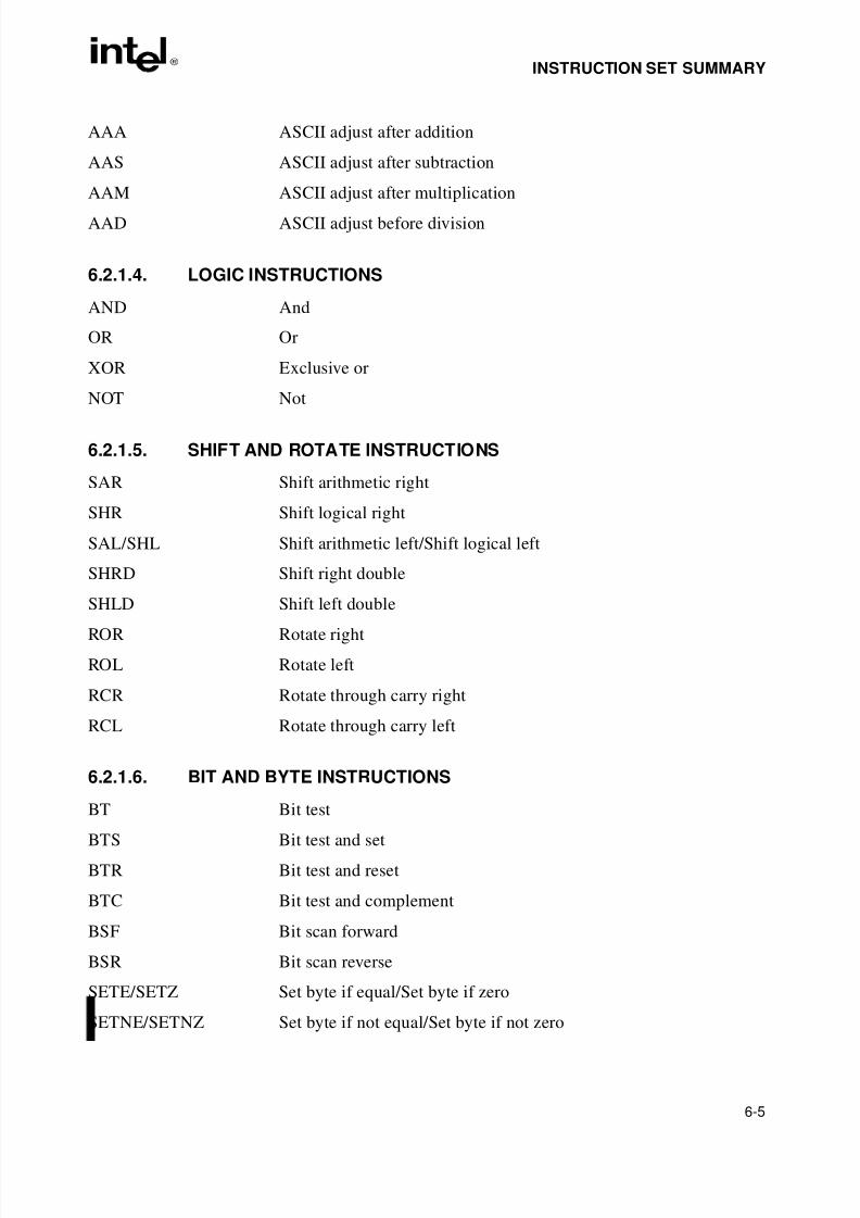
8/3/2019 Intel Architecture Software Developer's Manual, Volume 1: Basic Architecture
http://slidepdf.com/reader/full/intel-architecture-software-developers-manual-volume-1-basic-architecture 99/283
6-5
INSTRUCTION SET SUMMARY
AAA ASCII adjust after addition
AAS ASCII adjust after subtraction
AAM ASCII adjust after multiplication
AAD ASCII adjust before division
6.2.1.4. LOGIC INSTRUCTIONS
AND And
OR Or
XOR Exclusive or
NOT Not
6.2.1.5. SHIFT AND ROTATE INSTRUCTIONS
SAR Shift arithmetic right
SHR Shift logical right
SAL/SHL Shift arithmetic left/Shift logical left
SHRD Shift right double
SHLD Shift left double
ROR Rotate right
ROL Rotate left
RCR Rotate through carry right
RCL Rotate through carry left
6.2.1.6. BIT AND BYTE INSTRUCTIONS
BT Bit test
BTS Bit test and set
BTR Bit test and reset
BTC Bit test and complement
BSF Bit scan forward
BSR Bit scan reverse
SETE/SETZ Set byte if equal/Set byte if zero
SETNE/SETNZ Set byte if not equal/Set byte if not zero

8/3/2019 Intel Architecture Software Developer's Manual, Volume 1: Basic Architecture
http://slidepdf.com/reader/full/intel-architecture-software-developers-manual-volume-1-basic-architecture 100/283
6-6
INSTRUCTION SET SUMMARY
SETA/SETNBE Set byte if above/Set byte if not below or equal
SETAE/SETNB/SETNC Set byte if above or equal/Set byte if not below/Set byteif not carry
SETB/SETNAE/SETC Set byte if below/Set byte if not above or equal/Set byteif carry
SETBE/SETNA Set byte if below or equal/Set byte if not above
SETG/SETNLE Set byte if greater/Set byte if not less or equal
SETGE/SETNL Set byte if greater or equal/Set byte if not less
SETL/SETNGE Set byte if less/Set byte if not greater or equal
SETLE/SETNG Set byte if less or equal/Set byte if not greater
SETS Set byte if sign (negative)
SETNS Set byte if not sign (non-negative)
SETO Set byte if overflow
SETNO Set byte if not overflow
SETPE/SETP Set byte if parity even/Set byte if parity
SETPO/SETNP Set byte if parity odd/Set byte if not parity
TEST Logical compare
6.2.1.7. CONTROL TRANSFER INSTRUCTIONS
JMP Jump
JE/JZ Jump if equal/Jump if zero
JNE/JNZ Jump if not equal/Jump if not zero
JA/JNBE Jump if above/Jump if not below or equal
JAE/JNB Jump if above or equal/Jump if not below
JB/JNAE Jump if below/Jump if not above or equal
JBE/JNA Jump if below or equal/Jump if not above
JG/JNLE Jump if greater/Jump if not less or equal
JGE/JNL Jump if greater or equal/Jump if not less
JL/JNGE Jump if less/Jump if not greater or equal
JLE/JNG Jump if less or equal/Jump if not greater
JC Jump if carry
JNC Jump if not carry
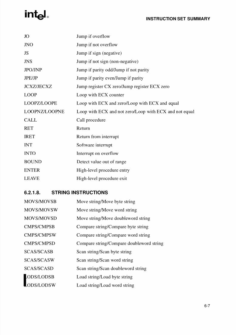
8/3/2019 Intel Architecture Software Developer's Manual, Volume 1: Basic Architecture
http://slidepdf.com/reader/full/intel-architecture-software-developers-manual-volume-1-basic-architecture 101/283
6-7
INSTRUCTION SET SUMMARY
JO Jump if overflow
JNO Jump if not overflow
JS Jump if sign (negative)
JNS Jump if not sign (non-negative)
JPO/JNP Jump if parity odd/Jump if not parity
JPE/JP Jump if parity even/Jump if parity
JCXZ/JECXZ Jump register CX zero/Jump register ECX zero
LOOP Loop with ECX counter
LOOPZ/LOOPE Loop with ECX and zero/Loop with ECX and equal
LOOPNZ/LOOPNE Loop with ECX and not zero/Loop with ECX and not equal
CALL Call procedure
RET Return
IRET Return from interrupt
INT Software interrupt
INTO Interrupt on overflow
BOUND Detect value out of range
ENTER High-level procedure entryLEAVE High-level procedure exit
6.2.1.8. STRING INSTRUCTIONS
MOVS/MOVSB Move string/Move byte string
MOVS/MOVSW Move string/Move word string
MOVS/MOVSD Move string/Move doubleword string
CMPS/CMPSB Compare string/Compare byte string
CMPS/CMPSW Compare string/Compare word string
CMPS/CMPSD Compare string/Compare doubleword string
SCAS/SCASB Scan string/Scan byte string
SCAS/SCASW Scan string/Scan word string
SCAS/SCASD Scan string/Scan doubleword string
LODS/LODSB Load string/Load byte string
LODS/LODSW Load string/Load word string
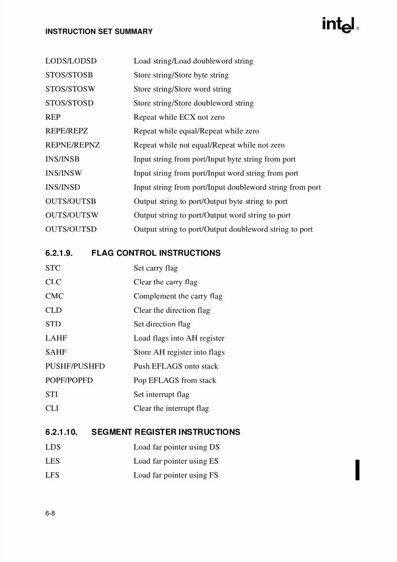
8/3/2019 Intel Architecture Software Developer's Manual, Volume 1: Basic Architecture
http://slidepdf.com/reader/full/intel-architecture-software-developers-manual-volume-1-basic-architecture 102/283
6-8
INSTRUCTION SET SUMMARY
LODS/LODSD Load string/Load doubleword string
STOS/STOSB Store string/Store byte string
STOS/STOSW Store string/Store word string
STOS/STOSD Store string/Store doubleword string
REP Repeat while ECX not zero
REPE/REPZ Repeat while equal/Repeat while zero
REPNE/REPNZ Repeat while not equal/Repeat while not zero
INS/INSB Input string from port/Input byte string from port
INS/INSW Input string from port/Input word string from port
INS/INSD Input string from port/Input doubleword string from port
OUTS/OUTSB Output string to port/Output byte string to port
OUTS/OUTSW Output string to port/Output word string to port
OUTS/OUTSD Output string to port/Output doubleword string to port
6.2.1.9. FLAG CONTROL INSTRUCTIONS
STC Set carry flag
CLC Clear the carry flag
CMC Complement the carry flag
CLD Clear the direction flag
STD Set direction flag
LAHF Load flags into AH register
SAHF Store AH register into flags
PUSHF/PUSHFD Push EFLAGS onto stack
POPF/POPFD Pop EFLAGS from stack
STI Set interrupt flag
CLI Clear the interrupt flag
6.2.1.10. SEGMENT REGISTER INSTRUCTIONS
LDS Load far pointer using DS
LES Load far pointer using ES
LFS Load far pointer using FS
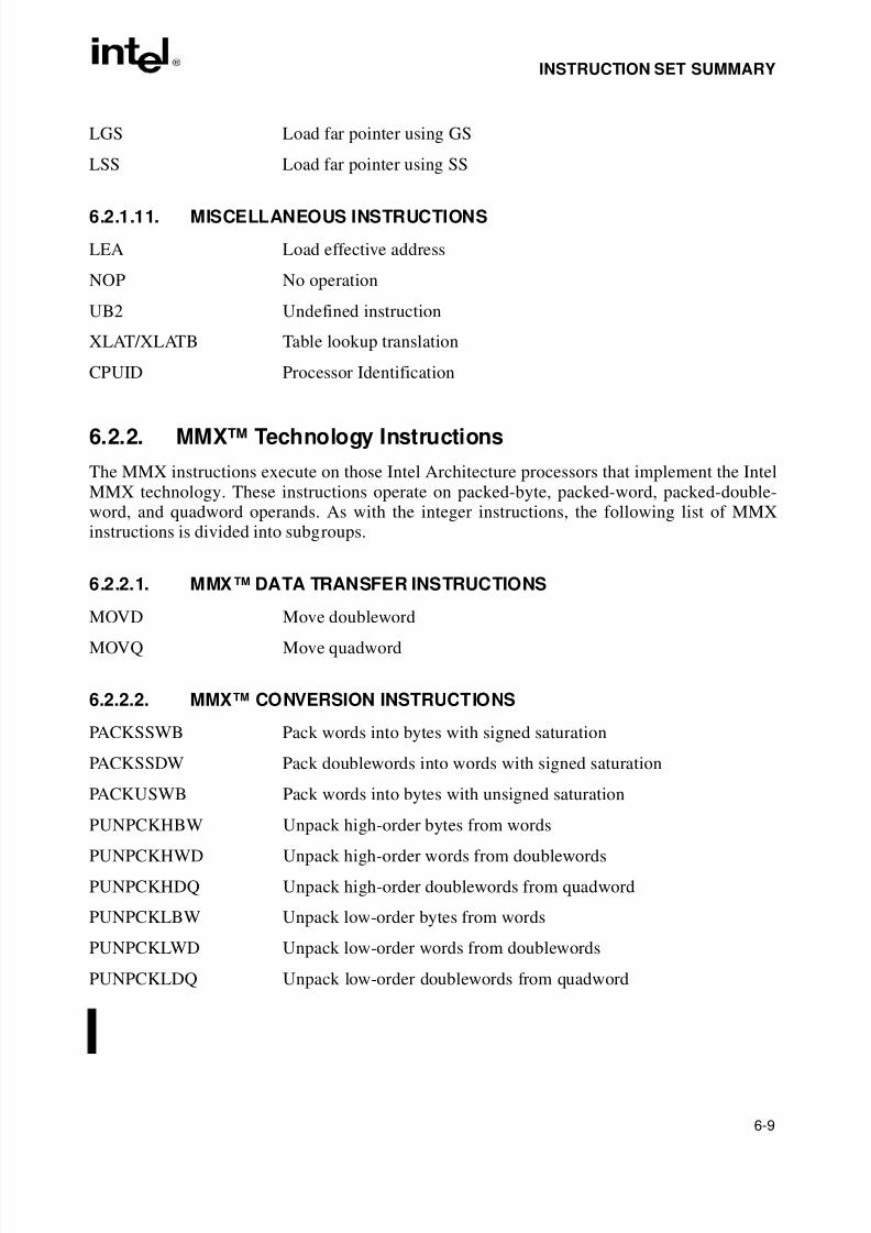
8/3/2019 Intel Architecture Software Developer's Manual, Volume 1: Basic Architecture
http://slidepdf.com/reader/full/intel-architecture-software-developers-manual-volume-1-basic-architecture 103/283
6-9
INSTRUCTION SET SUMMARY
LGS Load far pointer using GS
LSS Load far pointer using SS
6.2.1.11. MISCELLANEOUS INSTRUCTIONS
LEA Load effective address
NOP No operation
UB2 Undefined instruction
XLAT/XLATB Table lookup translation
CPUID Processor Identification
6.2.2. MMX™ Technology Instructions
The MMX instructions execute on those Intel Architecture processors that implement the IntelMMX technology. These instructions operate on packed-byte, packed-word, packed-double-word, and quadword operands. As with the integer instructions, the following list of MMXinstructions is divided into subgroups.
6.2.2.1. MMX™ DATA TRANSFER INSTRUCTIONS
MOVD Move doubleword
MOVQ Move quadword
6.2.2.2. MMX™ CONVERSION INSTRUCTIONS
PACKSSWB Pack words into bytes with signed saturation
PACKSSDW Pack doublewords into words with signed saturation
PACKUSWB Pack words into bytes with unsigned saturation
PUNPCKHBW Unpack high-order bytes from words
PUNPCKHWD Unpack high-order words from doublewords
PUNPCKHDQ Unpack high-order doublewords from quadword
PUNPCKLBW Unpack low-order bytes from words
PUNPCKLWD Unpack low-order words from doublewords
PUNPCKLDQ Unpack low-order doublewords from quadword
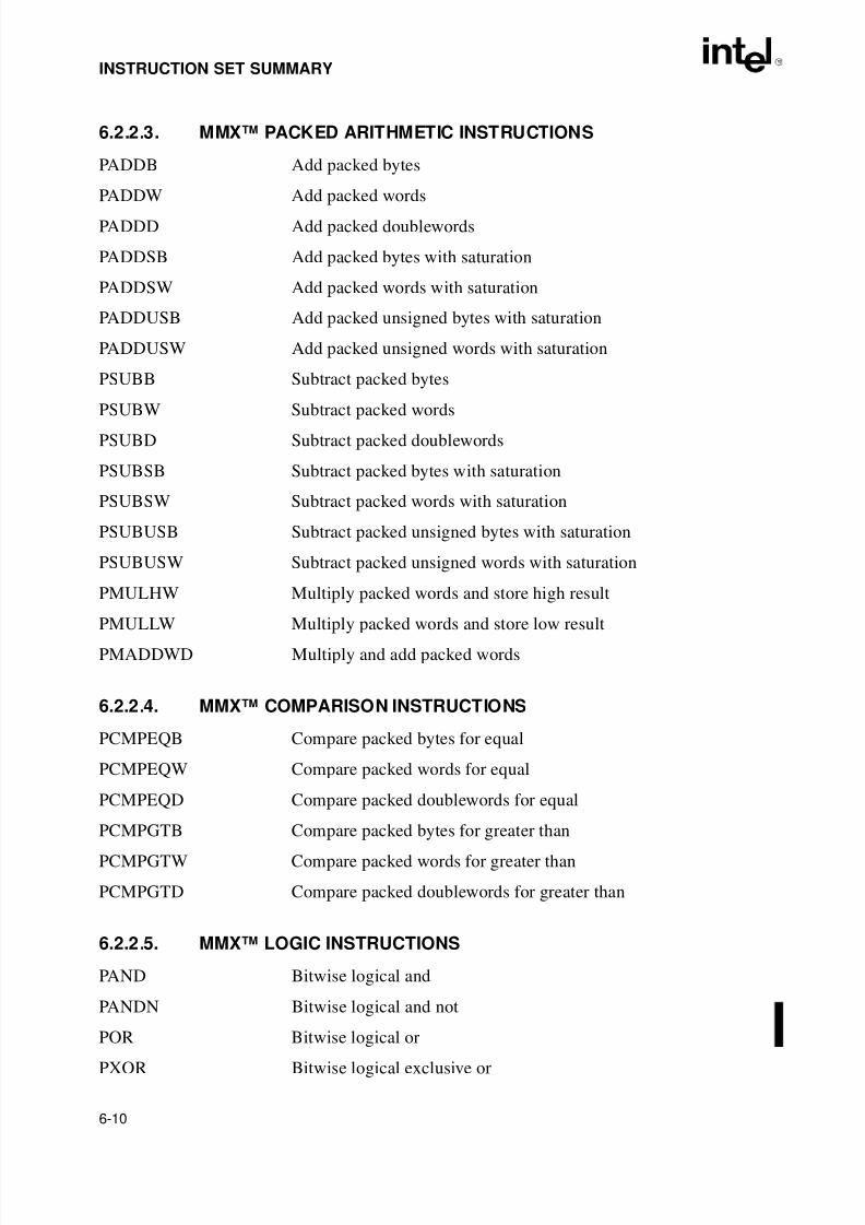
8/3/2019 Intel Architecture Software Developer's Manual, Volume 1: Basic Architecture
http://slidepdf.com/reader/full/intel-architecture-software-developers-manual-volume-1-basic-architecture 104/283
6-10
INSTRUCTION SET SUMMARY
6.2.2.3. MMX™ PACKED ARITHMETIC INSTRUCTIONS
PADDB Add packed bytes
PADDW Add packed words
PADDD Add packed doublewords
PADDSB Add packed bytes with saturation
PADDSW Add packed words with saturation
PADDUSB Add packed unsigned bytes with saturation
PADDUSW Add packed unsigned words with saturation
PSUBB Subtract packed bytes
PSUBW Subtract packed words
PSUBD Subtract packed doublewords
PSUBSB Subtract packed bytes with saturation
PSUBSW Subtract packed words with saturation
PSUBUSB Subtract packed unsigned bytes with saturation
PSUBUSW Subtract packed unsigned words with saturation
PMULHW Multiply packed words and store high result
PMULLW Multiply packed words and store low resultPMADDWD Multiply and add packed words
6.2.2.4. MMX™ COMPARISON INSTRUCTIONS
PCMPEQB Compare packed bytes for equal
PCMPEQW Compare packed words for equal
PCMPEQD Compare packed doublewords for equal
PCMPGTB Compare packed bytes for greater than
PCMPGTW Compare packed words for greater than
PCMPGTD Compare packed doublewords for greater than
6.2.2.5. MMX™ LOGIC INSTRUCTIONS
PAND Bitwise logical and
PANDN Bitwise logical and not
POR Bitwise logical or
PXOR Bitwise logical exclusive or
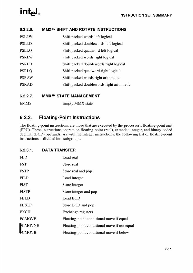
8/3/2019 Intel Architecture Software Developer's Manual, Volume 1: Basic Architecture
http://slidepdf.com/reader/full/intel-architecture-software-developers-manual-volume-1-basic-architecture 105/283
6-11
INSTRUCTION SET SUMMARY
6.2.2.6. MMX™ SHIFT AND ROTATE INSTRUCTIONS
PSLLW Shift packed words left logical
PSLLD Shift packed doublewords left logical
PSLLQ Shift packed quadword left logical
PSRLW Shift packed words right logical
PSRLD Shift packed doublewords right logical
PSRLQ Shift packed quadword right logical
PSRAW Shift packed words right arithmetic
PSRAD Shift packed doublewords right arithmetic
6.2.2.7. MMX™ STATE MANAGEMENT
EMMS Empty MMX state
6.2.3. Floating-Point Instructions
The floating-point instructions are those that are executed by the processor’s floating-point unit(FPU). These instructions operate on floating-point (real), extended integer, and binary-codeddecimal (BCD) operands. As with the integer instructions, the following list of floating-point
instructions is divided into subgroups.
6.2.3.1. DATA TRANSFER
FLD Load real
FST Store real
FSTP Store real and pop
FILD Load integer
FIST Store integer
FISTP Store integer and pop
FBLD Load BCD
FBSTP Store BCD and pop
FXCH Exchange registers
FCMOVE Floating-point conditional move if equal
FCMOVNE Floating-point conditional move if not equal
FCMOVB Floating-point conditional move if below
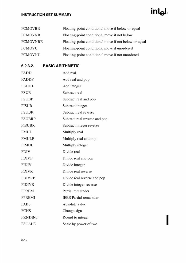
8/3/2019 Intel Architecture Software Developer's Manual, Volume 1: Basic Architecture
http://slidepdf.com/reader/full/intel-architecture-software-developers-manual-volume-1-basic-architecture 106/283
6-12
INSTRUCTION SET SUMMARY
FCMOVBE Floating-point conditional move if below or equal
FCMOVNB Floating-point conditional move if not below
FCMOVNBE Floating-point conditional move if not below or equal
FCMOVU Floating-point conditional move if unordered
FCMOVNU Floating-point conditional move if not unordered
6.2.3.2. BASIC ARITHMETIC
FADD Add real
FADDP Add real and pop
FIADD Add integer
FSUB Subtract real
FSUBP Subtract real and pop
FISUB Subtract integer
FSUBR Subtract real reverse
FSUBRP Subtract real reverse and pop
FISUBR Subtract integer reverse
FMUL Multiply real
FMULP Multiply real and pop
FIMUL Multiply integer
FDIV Divide real
FDIVP Divide real and pop
FIDIV Divide integer
FDIVR Divide real reverse
FDIVRP Divide real reverse and pop
FIDIVR Divide integer reverse
FPREM Partial remainder
FPREMI IEEE Partial remainder
FABS Absolute value
FCHS Change sign
FRNDINT Round to integer
FSCALE Scale by power of two
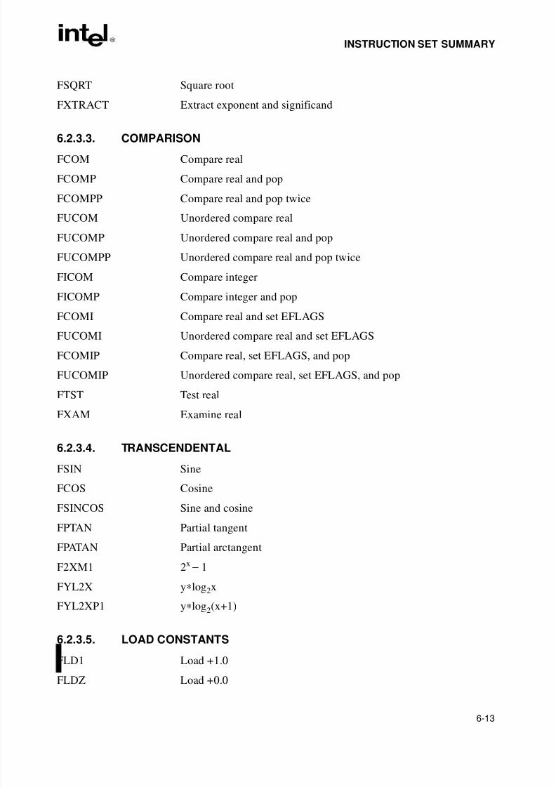
8/3/2019 Intel Architecture Software Developer's Manual, Volume 1: Basic Architecture
http://slidepdf.com/reader/full/intel-architecture-software-developers-manual-volume-1-basic-architecture 107/283
6-13
INSTRUCTION SET SUMMARY
FSQRT Square root
FXTRACT Extract exponent and significand
6.2.3.3. COMPARISON
FCOM Compare real
FCOMP Compare real and pop
FCOMPP Compare real and pop twice
FUCOM Unordered compare real
FUCOMP Unordered compare real and pop
FUCOMPP Unordered compare real and pop twice
FICOM Compare integer
FICOMP Compare integer and pop
FCOMI Compare real and set EFLAGS
FUCOMI Unordered compare real and set EFLAGS
FCOMIP Compare real, set EFLAGS, and pop
FUCOMIP Unordered compare real, set EFLAGS, and pop
FTST Test real
FXAM Examine real
6.2.3.4. TRANSCENDENTAL
FSIN Sine
FCOS Cosine
FSINCOS Sine and cosine
FPTAN Partial tangent
FPATAN Partial arctangent
F2XM1 2x − 1
FYL2X y∗log2x
FYL2XP1 y∗log2(x+1)
6.2.3.5. LOAD CONSTANTS
FLD1 Load +1.0
FLDZ Load +0.0
8/3/2019 Intel Architecture Software Developer's Manual, Volume 1: Basic Architecture
http://slidepdf.com/reader/full/intel-architecture-software-developers-manual-volume-1-basic-architecture 108/283
6-14
INSTRUCTION SET SUMMARY
FLDPI Load π
FLDL2E Load log2e
FLDLN2 Load loge2
FLDL2T Load log210
FLDLG2 Load log102
6.2.3.6. FPU CONTROL
FINCSTP Increment FPU register stack pointer
FDECSTP Decrement FPU register stack pointer
FFREE Free floating-point register
FINIT Initialize FPU after checking error conditions
FNINIT Initialize FPU without checking error conditions
FCLEX Clear floating-point exception flags after checking for errorconditions
FNCLEX Clear floating-point exception flags without checking for errorconditions
FSTCW Store FPU control word after checking error conditions
FNSTCW Store FPU control word without checking error conditionsFLDCW Load FPU control word
FSTENV Store FPU environment after checking error conditions
FNSTENV Store FPU environment without checking error conditions
FLDENV Load FPU environment
FSAVE Save FPU state after checking error conditions
FNSAVE Save FPU state without checking error conditions
FRSTOR Restore FPU state
FSTSW Store FPU status word after checking error conditions
FNSTSW Store FPU status word without checking error conditions
WAIT/FWAIT Wait for FPU
FNOP FPU no operation
8/3/2019 Intel Architecture Software Developer's Manual, Volume 1: Basic Architecture
http://slidepdf.com/reader/full/intel-architecture-software-developers-manual-volume-1-basic-architecture 109/283
6-15
INSTRUCTION SET SUMMARY
6.2.4. System Instructions
The following system instructions are used to control those functions of the processor that areprovided to support for operating systems and executives.
LGDT Load global descriptor table (GDT) register
SGDT Store global descriptor table (GDT) register
LLDT Load local descriptor table (LDT) register
SLDT Store local descriptor table (LDT) register
LTR Load task register
STR Store task register
LIDT Load interrupt descriptor table (IDT) register
SIDT Store interrupt descriptor table (IDT) register
MOV Load and store control registers
LMSW Load machine status word
SMSW Store machine status word
CLTS Clear the task-switched flag
ARPL Adjust requested privilege level
LAR Load access rights
LSL Load segment limit
VERR Verify segment for reading
VERW Verify segment for writing
MOV Load and store debug registers
INVD Invalidate cache, no writeback
WBINVD Invalidate cache, with writeback
INVLPG Invalidate TLB Entry
LOCK (prefix) Lock Bus
HLT Halt processor
RSM Return from system management mode (SSM)
RDMSR Read model-specific register
WRMSR Write model-specific register
RDPMC Read performance monitoring counters
RDTSC Read time stamp counter
8/3/2019 Intel Architecture Software Developer's Manual, Volume 1: Basic Architecture
http://slidepdf.com/reader/full/intel-architecture-software-developers-manual-volume-1-basic-architecture 110/283
6-16
INSTRUCTION SET SUMMARY
6.3. DATA MOVEMENT INSTRUCTIONS
The data movement instructions move bytes, words, doublewords, or quadwords both betweenmemory and the processor’s registers and between registers. These instructions are divided into
four groups:
• General-purpose data movement.
• Exchange.
• Stack manipulation.
• Type-conversion.
6.3.1. General-Purpose Data Movement Instructions
The MOV (move) and CMOVcc (conditional move) instructions transfer data between memoryand registers or between registers.
6.3.1.1. MOVE INSTRUCTION
The MOV instruction performs basic load data and store data operations between memory andthe processor’s registers and data movement operations between registers. It handles data trans-fers along the paths listed in Table 6-1. (See “MOV—Move to/from Control Registers” and“MOV—Move to/from Debug Registers” in Chapter 3 of the Intel Architecture Software Devel-oper’s Manual, Volume 2, for information on moving data to and from the control and debug
registers.)
The MOV instruction cannot move data from one memory location to another or from onesegment register to another segment register. Memory-to-memory moves can be performed withthe MOVS (string move) instruction (see Section 6.10., “String Operations”).
6.3.1.2. CONDITIONAL MOVE INSTRUCTIONS
The CMOVcc instructions are a group of instructions that check the state of the status flags inthe EFLAGS register and perform a move operation if the flags are in a specified state (or condi-tion). These instructions can be used to move a 16- or 32-bit value from memory to a general-
purpose register or from one general-purpose register to another. The flag state being tested foreach instruction is specified with a condition code (cc) that is associated with the instruction. If the condition is not satisfied, a move is not performed and execution continues with the instruc-tion following the CMOVcc instruction.
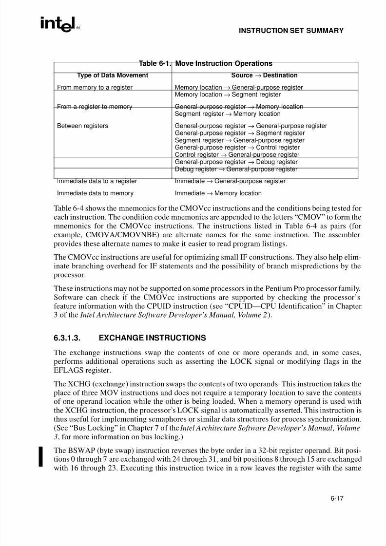
8/3/2019 Intel Architecture Software Developer's Manual, Volume 1: Basic Architecture
http://slidepdf.com/reader/full/intel-architecture-software-developers-manual-volume-1-basic-architecture 111/283
6-17
INSTRUCTION SET SUMMARY
Table 6-4 shows the mnemonics for the CMOVcc instructions and the conditions being tested foreach instruction. The condition code mnemonics are appended to the letters “CMOV” to form themnemonics for the CMOVcc instructions. The instructions listed in Table 6-4 as pairs (forexample, CMOVA/CMOVNBE) are alternate names for the same instruction. The assemblerprovides these alternate names to make it easier to read program listings.
The CMOVcc instructions are useful for optimizing small IF constructions. They also help elim-inate branching overhead for IF statements and the possibility of branch mispredictions by theprocessor.
These instructions may not be supported on some processors in the Pentium Pro processor family.Software can check if the CMOVcc instructions are supported by checking the processor’sfeature information with the CPUID instruction (see “CPUID—CPU Identification” in Chapter3 of the Intel Architecture Software Developer’s Manual, Volume 2).
6.3.1.3. EXCHANGE INSTRUCTIONS
The exchange instructions swap the contents of one or more operands and, in some cases,performs additional operations such as asserting the LOCK signal or modifying flags in theEFLAGS register.
The XCHG (exchange) instruction swaps the contents of two operands. This instruction takes theplace of three MOV instructions and does not require a temporary location to save the contentsof one operand location while the other is being loaded. When a memory operand is used withthe XCHG instruction, the processor’s LOCK signal is automatically asserted. This instruction isthus useful for implementing semaphores or similar data structures for process synchronization.(See “Bus Locking” in Chapter 7 of the Intel Architecture Software Developer’s Manual, Volume3, for more information on bus locking.)
The BSWAP (byte swap) instruction reverses the byte order in a 32-bit register operand. Bit posi-tions 0 through 7 are exchanged with 24 through 31, and bit positions 8 through 15 are exchanged
with 16 through 23. Executing this instruction twice in a row leaves the register with the same
Table 6-1. Move Instruction Operations
Type of Data Movement Source → Destination
From memory to a register Memory location → General-purpose register
Memory location → Segment register
From a register to memory General-purpose register → Memory locationSegment register → Memory location
Between registers General-purpose register → General-purpose registerGeneral-purpose register → Segment registerSegment register → General-purpose registerGeneral-purpose register → Control registerControl register → General-purpose registerGeneral-purpose register → Debug registerDebug register → General-purpose register
Immediate data to a register Immediate → General-purpose register
Immediate data to memory Immediate → Memory location
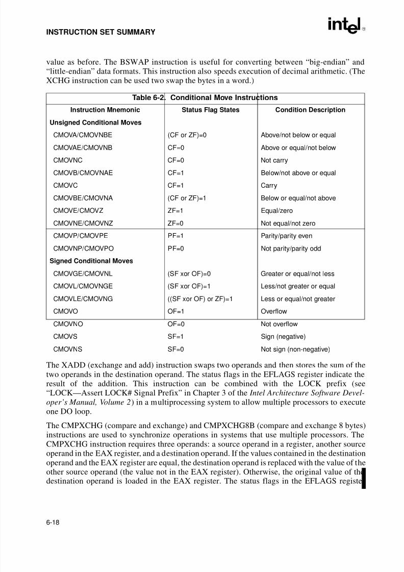
8/3/2019 Intel Architecture Software Developer's Manual, Volume 1: Basic Architecture
http://slidepdf.com/reader/full/intel-architecture-software-developers-manual-volume-1-basic-architecture 112/283
6-18
INSTRUCTION SET SUMMARY
value as before. The BSWAP instruction is useful for converting between “big-endian” and“little-endian” data formats. This instruction also speeds execution of decimal arithmetic. (TheXCHG instruction can be used two swap the bytes in a word.)
The XADD (exchange and add) instruction swaps two operands and then stores the sum of thetwo operands in the destination operand. The status flags in the EFLAGS register indicate theresult of the addition. This instruction can be combined with the LOCK prefix (see
“LOCK—Assert LOCK# Signal Prefix” in Chapter 3 of the Intel Architecture Software Devel-oper’s Manual, Volume 2) in a multiprocessing system to allow multiple processors to executeone DO loop.
The CMPXCHG (compare and exchange) and CMPXCHG8B (compare and exchange 8 bytes)instructions are used to synchronize operations in systems that use multiple processors. TheCMPXCHG instruction requires three operands: a source operand in a register, another sourceoperand in the EAX register, and a destination operand. If the values contained in the destinationoperand and the EAX register are equal, the destination operand is replaced with the value of theother source operand (the value not in the EAX register). Otherwise, the original value of thedestination operand is loaded in the EAX register. The status flags in the EFLAGS register
Table 6-2. Conditional Move InstructionsInstruction Mnemonic Status Flag States Condition Description
Unsigned Conditional Moves
CMOVA/CMOVNBE (CF or ZF)=0 Above/not below or equal
CMOVAE/CMOVNB CF=0 Above or equal/not below
CMOVNC CF=0 Not carry
CMOVB/CMOVNAE CF=1 Below/not above or equal
CMOVC CF=1 Carry
CMOVBE/CMOVNA (CF or ZF)=1 Below or equal/not above
CMOVE/CMOVZ ZF=1 Equal/zero
CMOVNE/CMOVNZ ZF=0 Not equal/not zero
CMOVP/CMOVPE PF=1 Parity/parity even
CMOVNP/CMOVPO PF=0 Not parity/parity odd
Signed Conditional Moves
CMOVGE/CMOVNL (SF xor OF)=0 Greater or equal/not less
CMOVL/CMOVNGE (SF xor OF)=1 Less/not greater or equal
CMOVLE/CMOVNG ((SF xor OF) or ZF)=1 Less or equal/not greater
CMOVO OF=1 Overflow
CMOVNO OF=0 Not overflow
CMOVS SF=1 Sign (negative)
CMOVNS SF=0 Not sign (non-negative)
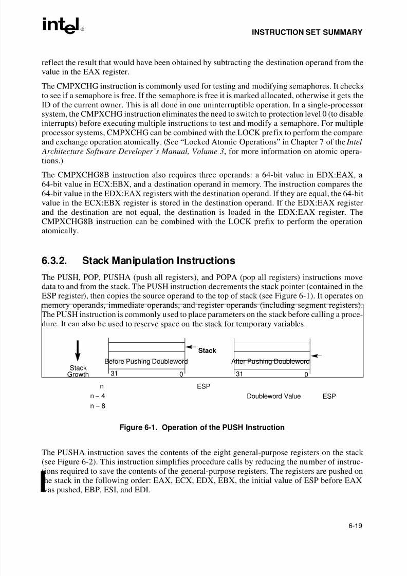
8/3/2019 Intel Architecture Software Developer's Manual, Volume 1: Basic Architecture
http://slidepdf.com/reader/full/intel-architecture-software-developers-manual-volume-1-basic-architecture 113/283
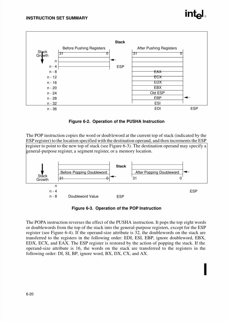
8/3/2019 Intel Architecture Software Developer's Manual, Volume 1: Basic Architecture
http://slidepdf.com/reader/full/intel-architecture-software-developers-manual-volume-1-basic-architecture 114/283
6-20
INSTRUCTION SET SUMMARY
The POP instruction copies the word or doubleword at the current top of stack (indicated by theESP register) to the location specified with the destination operand, and then increments the ESPregister to point to the new top of stack (see Figure 6-3). The destination operand may specify ageneral-purpose register, a segment register, or a memory location.
The POPA instruction reverses the effect of the PUSHA instruction. It pops the top eight wordsor doublewords from the top of the stack into the general-purpose registers, except for the ESPregister (see Figure 6-4). If the operand-size attribute is 32, the doublewords on the stack aretransferred to the registers in the following order: EDI, ESI, EBP, ignore doubleword, EBX,EDX, ECX, and EAX. The ESP register is restored by the action of popping the stack. If theoperand-size attribute is 16, the words on the stack are transferred to the registers in thefollowing order: DI, SI, BP, ignore word, BX, DX, CX, and AX.
Figure 6-2. Operation of the PUSHA Instruction
Figure 6-3. Operation of the POP Instruction
0
Stack
31
Before Pushing Registers
Growth
ESPn - 4
n - 8
n
Stack
031
After Pushing Registers
ESP
EAX
EDI
EBX
EBP
ECX
EDX
Old ESP
ESI
n - 36
n - 20
n - 28
n - 12
n - 16
n - 24
n - 32
031Stack
After Popping Doubleword
Growth
ESPn - 4
n - 8
n
Stack
Before Popping Doubleword
ESPDoubleword Value
031
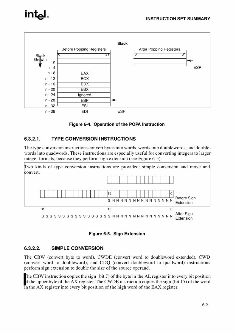
8/3/2019 Intel Architecture Software Developer's Manual, Volume 1: Basic Architecture
http://slidepdf.com/reader/full/intel-architecture-software-developers-manual-volume-1-basic-architecture 115/283
6-21
INSTRUCTION SET SUMMARY
6.3.2.1. TYPE CONVERSION INSTRUCTIONS
The type conversion instructions convert bytes into words, words into doublewords, and double-words into quadwords. These instructions are especially useful for converting integers to largerinteger formats, because they perform sign extension (see Figure 6-5).
Two kinds of type conversion instructions are provided: simple conversion and move and
convert.
6.3.2.2. SIMPLE CONVERSION
The CBW (convert byte to word), CWDE (convert word to doubleword extended), CWD(convert word to doubleword), and CDQ (convert doubleword to quadword) instructionsperform sign extension to double the size of the source operand.
The CBW instruction copies the sign (bit 7) of the byte in the AL register into every bit positionof the upper byte of the AX register. The CWDE instruction copies the sign (bit 15) of the word
in the AX register into every bit position of the high word of the EAX register.
Figure 6-4. Operation of the POPA Instruction
Figure 6-5. Sign Extension
Stack
After Popping Registers
Growth
ESPn - 4
n - 8
n
Stack
Before Popping Registers
ESP
EAX
EDI
EBX
EBP
ECX
EDX
Ignored
ESI
n - 36
n - 20
n - 28
n - 12
n - 16
n - 24
n - 32
0 310 31
31
After Sign
15 0
S N N N N N N N N N NN N N N NSSSSSSSSSSSS SSSSExtension
Before Sign15 0
S N N N N N N N N N NN N N N NExtension
8/3/2019 Intel Architecture Software Developer's Manual, Volume 1: Basic Architecture
http://slidepdf.com/reader/full/intel-architecture-software-developers-manual-volume-1-basic-architecture 116/283
6-22
INSTRUCTION SET SUMMARY
The CWD instruction copies the sign (bit 15) of the word in the AX register into every bit posi-tion in the DX register. The CDQ instruction copies the sign (bit 31) of the doubleword in theEAX register into every bit position in the EDX register. The CWD instruction can be used toproduce a doubleword dividend from a word before a word division, and the CDQ instruction
can be used to produce a quadword dividend from a doubleword before doubleword division.
6.3.2.3. MOVE AND CONVERT
The MOVSX (move with sign extension) and MOVZX (move with zero extension) instructionsmove the source operand into a register then perform the sign extension.
The MOVSX instruction extends an 8-bit value to a 16-bit value or an 8- or 16-bit value to 32-bitvalue by sign extending the source operand, as shown in Figure 6-5. The MOVZX instructionextends an 8-bit value to a 16-bit value or an 8- or 16-bit value to 32-bit value by zero extendingthe source operand.
6.4. BINARY ARITHMETIC INSTRUCTIONS
The binary arithmetic instructions operate on 8-, 16-, and 32-bit numeric data encoded as signedor unsigned binary integers. Operations include the add, subtract, multiply, and divide as well asincrement, decrement, compare, and change sign (negate). The binary arithmetic instructionsmay also be used in algorithms that operate on decimal (BCD) values.
6.4.1. Addition and Subtraction InstructionsThe ADD (add integers), ADC (add integers with carry), SUB (subtract integers), and SBB(subtract integers with borrow) instructions perform addition and subtraction operations onsigned or unsigned integer operands.
The ADD instruction computes the sum of two integer operands.
The ADC instruction computes the sum of two integer operands, plus 1 if the CF flag is set. Thisinstruction is used to propagate a carry when adding numbers in stages.
The SUB instruction computes the difference of two integer operands.
The SBB instruction computes the difference of two integer operands, minus 1 if the CF flag isset. This instruction is used to propagate a borrow when subtracting numbers in stages.
6.4.2. Increment and Decrement Instructions
The INC (increment) and DEC (decrement) instructions add 1 to or subtract 1 from an unsignedinteger operand, respectively. A primary use of these instructions is for implementing counters.
8/3/2019 Intel Architecture Software Developer's Manual, Volume 1: Basic Architecture
http://slidepdf.com/reader/full/intel-architecture-software-developers-manual-volume-1-basic-architecture 117/283
6-23
INSTRUCTION SET SUMMARY
6.4.3. Comparison and Sign Change Instruction
The CMP (compare) instruction computes the difference between two integer operands andupdates the OF, SF, ZF, AF, PF, and CF flags according to the result. The source operands are
not modified, nor is the result saved. The CMP instruction is commonly used in conjunction witha Jcc (jump) or SETcc (byte set on condition) instruction, with the latter instructions performingan action based on the result of a CMP instruction.
The NEG (negate) instruction subtracts a signed integer operand from zero. The effect of theNEG instruction is to change the sign of a two's complement operand while keeping itsmagnitude.
6.4.4. Multiplication and Divide Instructions
The processor provides two multiply instructions, MUL (unsigned multiply) and IMUL signedmultiply), and two divide instructions, DIV (unsigned divide) and IDIV (signed divide).
The MUL instruction multiplies two unsigned integer operands. The result is computed to twicethe size of the source operands (for example, if word operands are being multiplied, the result isa doubleword).
The IMUL instruction multiplies two signed integer operands. The result is computed to twicethe size of the source operands; however, in some cases the result is truncated to the size of thesource operands (see “IMUL—Signed Multiply” in Chapter 3 of the Intel Architecture Software
Developer’s Manual, Volume 2).
The DIV instruction divides one unsigned operand by another unsigned operand and returns aquotient and a remainder.
The IDIV instruction is identical to the DIV instruction, except that IDIV performs a signeddivision.
6.5. DECIMAL ARITHMETIC INSTRUCTIONS
Decimal arithmetic can be performed by combining the binary arithmetic instructions ADD,SUB, MUL, and DIV (discussed in Section 6.4., “Binary Arithmetic Instructions”) with the
decimal arithmetic instructions. The decimal arithmetic instructions are provided to carry out thefollowing operations:
• To adjust the results of a previous binary arithmetic operation to produce a valid BCDresult.
• To adjust the operands of a subsequent binary arithmetic operation so that the operationwill produce a valid BCD result.
These instructions operate only on both packed and unpacked BCD values.
8/3/2019 Intel Architecture Software Developer's Manual, Volume 1: Basic Architecture
http://slidepdf.com/reader/full/intel-architecture-software-developers-manual-volume-1-basic-architecture 118/283
6-24
INSTRUCTION SET SUMMARY
6.5.1. Packed BCD Adjustment Instructions
The DAA (decimal adjust after addition) and DAS (decimal adjust after subtraction) instructionsadjust the results of operations performed on packed BCD integers (see Section 5.2.3., “BCD
Integers”). Adding two packed BCD values requires two instructions: an ADD instructionfollowed by a DAA instruction. The ADD instruction adds (binary addition) the two values andstores the result in the AL register. The DAA instruction then adjusts the value in the AL registerto obtain a valid, 2-digit, packed BCD value and sets the CF flag if a decimal carry occurred asthe result of the addition.
Likewise, subtracting one packed BCD value from another requires a SUB instruction followedby a DAS instruction. The SUB instruction subtracts (binary subtraction) one BCD value fromanother and stores the result in the AL register. The DAS instruction then adjusts the value in theAL register to obtain a valid, 2-digit, packed BCD value and sets the CF flag if a decimal borrowoccurred as the result of the subtraction.
6.5.2. Unpacked BCD Adjustment Instructions
The AAA (ASCII adjust after addition), AAS (ASCII adjust after subtraction), AAM (ASCIIadjust after multiplication), and AAD (ASCII adjust before division) instructions adjust theresults of arithmetic operations performed in unpacked BCD values (see Section 5.2.3.,“BCD Integers”). All these instructions assume that the value to be adjusted is stored in the ALregister or, in one instance, the AL and AH registers.
The AAA instruction adjusts the contents of the AL register following the addition of two
unpacked BCD values. It converts the binary value in the AL register into a decimal value andstores the result in the AL register in unpacked BCD format (the decimal number is stored in thelower 4 bits of the register and the upper 4 bits are cleared). If a decimal carry occurred as a resultof the addition, the CF flag is set and the contents of the AH register are incremented by 1.
The AAS instruction adjusts the contents of the AL register following the subtraction of twounpacked BCD values. Here again, a binary value is converted into an unpacked BCD value. If a borrow was required to complete the decimal subtract, the CF flag is set and the contents of the AH register are decremented by 1.
The AAM instruction adjusts the contents of the AL register following a multiplication of twounpacked BCD values. It converts the binary value in the AL register into a decimal value and
stores the least significant digit of the result in the AL register (in unpacked BCD format) andthe most significant digit, if there is one, in the AH register (also in unpacked BCD format).
The AAD instruction adjusts a two-digit BCD value so that when the value is divided with theDIV instruction, a valid unpacked BCD result is obtained. The instruction converts the BCDvalue in registers AH (most significant digit) and AL (least significant digit) into a binary valueand stores the result in register AL. When the value in AL is divided by an unpacked BCD value,the quotient and remainder will be automatically encoded in unpacked BCD format.
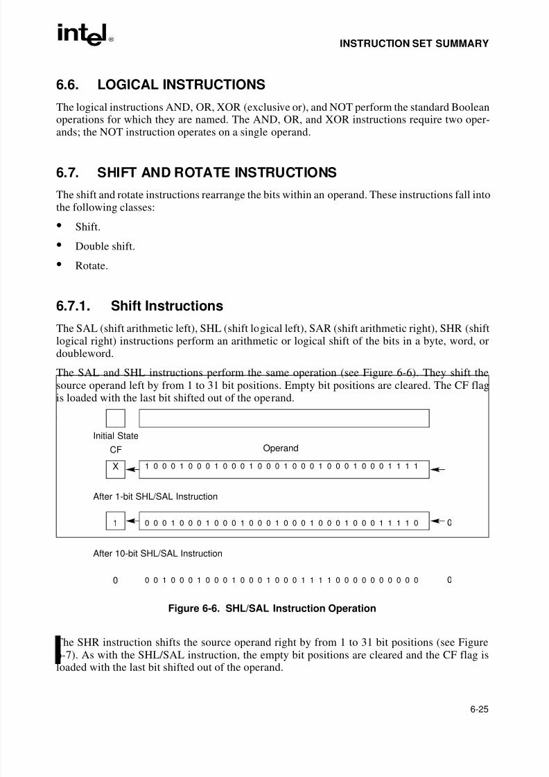
8/3/2019 Intel Architecture Software Developer's Manual, Volume 1: Basic Architecture
http://slidepdf.com/reader/full/intel-architecture-software-developers-manual-volume-1-basic-architecture 119/283
6-25
INSTRUCTION SET SUMMARY
6.6. LOGICAL INSTRUCTIONS
The logical instructions AND, OR, XOR (exclusive or), and NOT perform the standard Booleanoperations for which they are named. The AND, OR, and XOR instructions require two oper-
ands; the NOT instruction operates on a single operand.
6.7. SHIFT AND ROTATE INSTRUCTIONS
The shift and rotate instructions rearrange the bits within an operand. These instructions fall intothe following classes:
• Shift.
• Double shift.
• Rotate.
6.7.1. Shift Instructions
The SAL (shift arithmetic left), SHL (shift logical left), SAR (shift arithmetic right), SHR (shiftlogical right) instructions perform an arithmetic or logical shift of the bits in a byte, word, ordoubleword.
The SAL and SHL instructions perform the same operation (see Figure 6-6). They shift thesource operand left by from 1 to 31 bit positions. Empty bit positions are cleared. The CF flag
is loaded with the last bit shifted out of the operand..
The SHR instruction shifts the source operand right by from 1 to 31 bit positions (see Figure6-7). As with the SHL/SAL instruction, the empty bit positions are cleared and the CF flag is
loaded with the last bit shifted out of the operand.
Figure 6-6. SHL/SAL Instruction Operation
1 0 0 0 1 0 0 0 1 0 0 0 1 0 0 0 1 0 0 0 1 0 0 0 1 0 0 0 1 1 1 1X
Initial State
CF
00 0 0 1 0 0 0 1 0 0 0 1 0 0 0 1 0 0 0 1 0 0 0 1 0 0 0 1 1 1 1 01
After 1-bit SHL/SAL Instruction
00 0 1 0 0 0 1 0 0 0 1 0 0 0 1 0 0 0 1 1 1 1 0 0 0 0 0 0 0 0 0 00
After 10-bit SHL/SAL Instruction
Operand
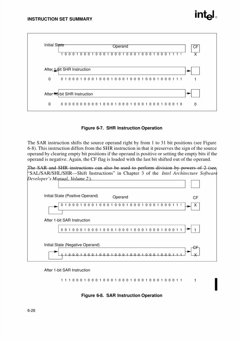
8/3/2019 Intel Architecture Software Developer's Manual, Volume 1: Basic Architecture
http://slidepdf.com/reader/full/intel-architecture-software-developers-manual-volume-1-basic-architecture 120/283
6-26
INSTRUCTION SET SUMMARY
The SAR instruction shifts the source operand right by from 1 to 31 bit positions (see Figure6-8). This instruction differs from the SHR instruction in that it preserves the sign of the sourceoperand by clearing empty bit positions if the operand is positive or setting the empty bits if theoperand is negative. Again, the CF flag is loaded with the last bit shifted out of the operand.
The SAR and SHR instructions can also be used to perform division by powers of 2 (see
“SAL/SAR/SHL/SHR—Shift Instructions” in Chapter 3 of the Intel Architecture Software Developer’s Manual, Volume 2).
Figure 6-7. SHR Instruction Operation
Figure 6-8. SAR Instruction Operation
1 0 0 0 1 0 0 0 1 0 0 0 1 0 0 0 1 0 0 0 1 0 0 0 1 0 0 0 1 1 1 1 X
Initial StateCF
00 1 0 0 0 1 0 0 0 1 0 0 0 1 0 0 0 1 0 0 0 1 0 0 0 1 0 0 0 1 1 1 1
After 1-bit SHR Instruction
00 0 0 0 0 0 0 0 0 0 1 0 0 0 1 0 0 0 1 0 0 0 1 0 0 0 1 0 0 0 1 0 0
After 10-bit SHR Instruction
Operand
0 1 0 0 0 1 0 0 0 1 0 0 0 1 0 0 0 1 0 0 0 1 0 0 0 1 0 0 0 1 1 1 X
Initial State (Positive Operand)CF
0 0 1 0 0 0 1 0 0 0 1 0 0 0 1 0 0 0 1 0 0 0 1 0 0 0 1 0 0 0 1 1 1
After 1-bit SAR Instruction
1 1 0 0 0 1 0 0 0 1 0 0 0 1 0 0 0 1 0 0 0 1 0 0 0 1 0 0 0 1 1 1 X
Initial State (Negative Operand)
Operand
1 1 1 0 0 0 1 0 0 0 1 0 0 0 1 0 0 0 1 0 0 0 1 0 0 0 1 0 0 0 1 1 1
After 1-bit SAR Instruction
CF
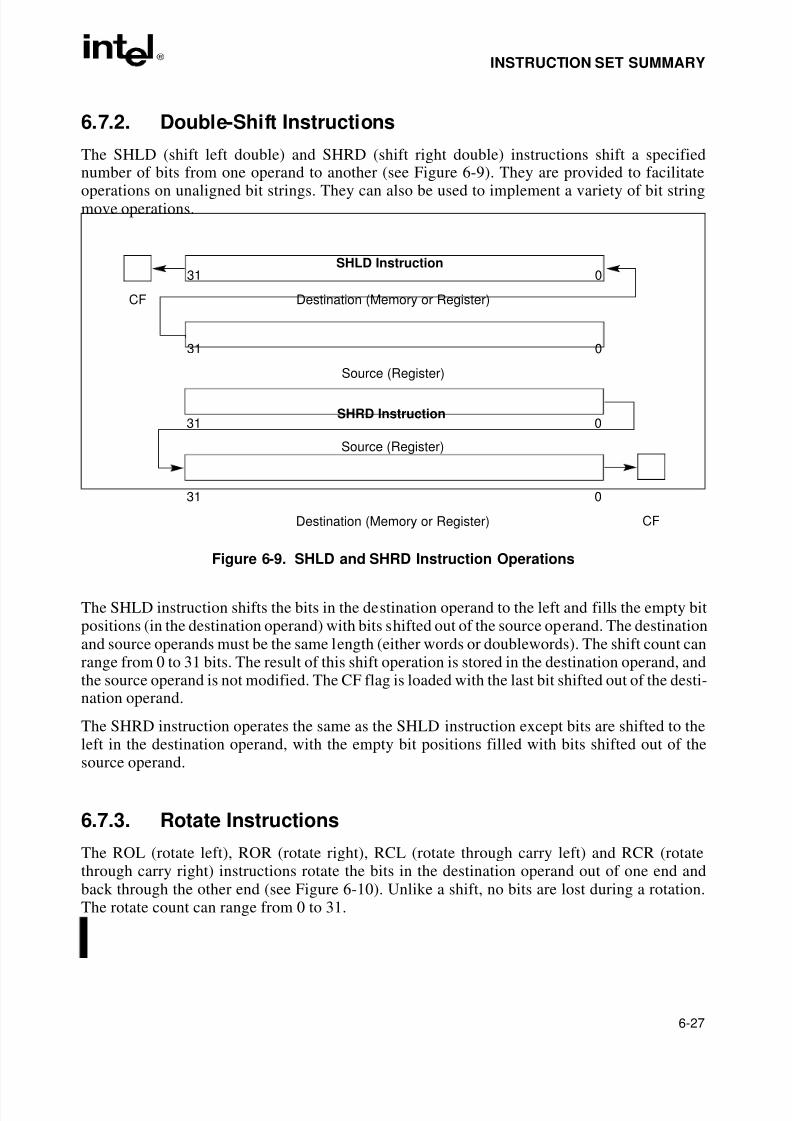
8/3/2019 Intel Architecture Software Developer's Manual, Volume 1: Basic Architecture
http://slidepdf.com/reader/full/intel-architecture-software-developers-manual-volume-1-basic-architecture 121/283
6-27
INSTRUCTION SET SUMMARY
6.7.2. Double-Shift Instructions
The SHLD (shift left double) and SHRD (shift right double) instructions shift a specifiednumber of bits from one operand to another (see Figure 6-9). They are provided to facilitate
operations on unaligned bit strings. They can also be used to implement a variety of bit stringmove operations.
The SHLD instruction shifts the bits in the destination operand to the left and fills the empty bitpositions (in the destination operand) with bits shifted out of the source operand. The destinationand source operands must be the same length (either words or doublewords). The shift count canrange from 0 to 31 bits. The result of this shift operation is stored in the destination operand, andthe source operand is not modified. The CF flag is loaded with the last bit shifted out of the desti-nation operand.
The SHRD instruction operates the same as the SHLD instruction except bits are shifted to theleft in the destination operand, with the empty bit positions filled with bits shifted out of the
source operand.
6.7.3. Rotate Instructions
The ROL (rotate left), ROR (rotate right), RCL (rotate through carry left) and RCR (rotatethrough carry right) instructions rotate the bits in the destination operand out of one end andback through the other end (see Figure 6-10). Unlike a shift, no bits are lost during a rotation.The rotate count can range from 0 to 31.
Figure 6-9. SHLD and SHRD Instruction Operations
Destination (Memory or Register)CF
31 0
Source (Register)
31 0
Destination (Memory or Register) CF
31 0
Source (Register)
31 0
SHRD Instruction
SHLD Instruction

8/3/2019 Intel Architecture Software Developer's Manual, Volume 1: Basic Architecture
http://slidepdf.com/reader/full/intel-architecture-software-developers-manual-volume-1-basic-architecture 122/283
6-28
INSTRUCTION SET SUMMARY
The ROL instruction rotates the bits in the operand to the left (toward more significant bit loca-tions). The ROR instruction rotates the operand right (toward less significant bit locations).
The RCL instruction rotates the bits in the operand to the left, through the CF flag). This instruc-tion treats the CF flag as a one-bit extension on the upper end of the operand. Each bit whichexits from the most significant bit location of the operand moves into the CF flag. At the sametime, the bit in the CF flag enters the least significant bit location of the operand.
The RCR instruction rotates the bits in the operand to the right through the CF flag.
For all the rotate instructions, the CF flag always contains the value of the last bit rotated out of the operand, even if the instruction does not use the CF flag as an extension of the operand. Thevalue of this flag can then be tested by a conditional jump instruction (JC or JNC).
Figure 6-10. ROL, ROR, RCL, and RCR Instruction Operations
Destination (Memory or Register)CF
31 0
Destination (Memory or Register) CF
031
Destination (Memory or Register)CF
31 0
Destination (Memory or Register) CF
31 0
ROL Instruction
RCL Instruction
RCR Instruction
ROR Instruction
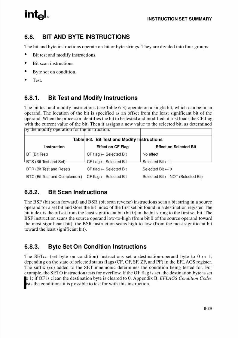
8/3/2019 Intel Architecture Software Developer's Manual, Volume 1: Basic Architecture
http://slidepdf.com/reader/full/intel-architecture-software-developers-manual-volume-1-basic-architecture 123/283
6-29
INSTRUCTION SET SUMMARY
6.8. BIT AND BYTE INSTRUCTIONS
The bit and byte instructions operate on bit or byte strings. They are divided into four groups:
•Bit test and modify instructions.
• Bit scan instructions.
• Byte set on condition.
• Test.
6.8.1. Bit Test and Modify Instructions
The bit test and modify instructions (see Table 6-3) operate on a single bit, which can be in anoperand. The location of the bit is specified as an offset from the least significant bit of theoperand. When the processor identifies the bit to be tested and modified, it first loads the CF flagwith the current value of the bit. Then it assigns a new value to the selected bit, as determinedby the modify operation for the instruction.
6.8.2. Bit Scan Instructions
The BSF (bit scan forward) and BSR (bit scan reverse) instructions scan a bit string in a sourceoperand for a set bit and store the bit index of the first set bit found in a destination register. Thebit index is the offset from the least significant bit (bit 0) in the bit string to the first set bit. TheBSF instruction scans the source operand low-to-high (from bit 0 of the source operand towardthe most significant bit); the BSR instruction scans high-to-low (from the most significant bittoward the least significant bit).
6.8.3. Byte Set On Condition Instructions
The SETcc (set byte on condition) instructions set a destination-operand byte to 0 or 1,depending on the state of selected status flags (CF, OF, SF, ZF, and PF) in the EFLAGS register.The suffix (cc) added to the SET mnemonic determines the condition being tested for. Forexample, the SETO instruction tests for overflow. If the OF flag is set, the destination byte is setto 1; if OF is clear, the destination byte is cleared to 0. Appendix B, EFLAGS Condition Codeslists the conditions it is possible to test for with this instruction.
Table 6-3. Bit Test and Modify Instructions
Instruction Effect on CF Flag Effect on Selected Bit
BT (Bit Test) CF flag ← Selected Bit No effect
BTS (Bit Test and Set) CF flag ← Selected Bit Selected Bit ← 1
BTR (Bit Test and Reset) CF flag ← Selected Bit Selected Bit ← 0
BTC (Bit Test and Complement) CF flag ← Selected Bit Selected Bit ← NOT (Selected Bit)
8/3/2019 Intel Architecture Software Developer's Manual, Volume 1: Basic Architecture
http://slidepdf.com/reader/full/intel-architecture-software-developers-manual-volume-1-basic-architecture 124/283
8/3/2019 Intel Architecture Software Developer's Manual, Volume 1: Basic Architecture
http://slidepdf.com/reader/full/intel-architecture-software-developers-manual-volume-1-basic-architecture 125/283
6-31
INSTRUCTION SET SUMMARY
6.9.1.2. CALL AND RETURN INSTRUCTIONS
The CALL (call procedure) and RET (return from procedure) instructions allow a jump fromone procedure (or subroutine) to another and a subsequent jump back (return) to the calling
procedure.The CALL instruction transfers program control from the current (or calling procedure) toanother procedure (the called procedure). To allow a subsequent return to the calling procedure,the CALL instruction saves the current contents of the EIP register on the stack before jumpingto the called procedure. The EIP register (prior to transferring program control) contains theaddress of the instruction following the CALL instruction. When this address is pushed on thestack, it is referred to as the return instruction pointer or return address.
The address of the called procedure (the address of the first instruction in the procedure being jumped to) is specified in a CALL instruction the same way as it is in a JMP instruction (seeSection 6.9.1.1., “Jump Instruction”). The address can be specified as a relative address or an
absolute address. If an absolute address is specified, it can be either a near or a far pointer.
The RET instruction transfers program control from the procedure currently being executed (thecalled procedure) back to the procedure that called it (the calling procedure). Transfer of controlis accomplished by copying the return instruction pointer from the stack into the EIP register.Program execution then continues with the instruction pointed to by the EIP register.
The RET instruction has an optional operand, the value of which is added to the contents of theESP register as part of the return operation. This operand allows the stack pointer to be incre-mented to remove parameters from the stack that were pushed on the stack by the callingprocedure.
See Section 4.3., “Calling Procedures Using CALL and RET”, for more information on themechanics of making procedure calls with the CALL and RET instructions.
6.9.1.3. RETURN FROM INTERRUPT INSTRUCTION
When the processor services an interrupt, it performs an implicit call to an interrupt-handlingprocedure. The IRET (return from interrupt) instruction returns program control from an inter-rupt handler to the interrupted procedure (that is, the procedure that was executing when theinterrupt occurred). The IRET instruction performs a similar operation to the RET instruction(see Section 6.9.1.2., “Call and Return Instructions”) except that it also restores the EFLAGS
register from the stack. The contents of the EFLAGS register are automatically stored on thestack along with the return instruction pointer when the processor services an interrupt.
6.9.2. Conditional Transfer Instructions
The conditional transfer instructions execute jumps or loops that transfer program control toanother instruction in the instruction stream if specified conditions are met. The conditions forcontrol transfer are specified with a set of condition codes that define various states of the statusflags (CF, ZF, OF, PF, and SF) in the EFLAGS register.
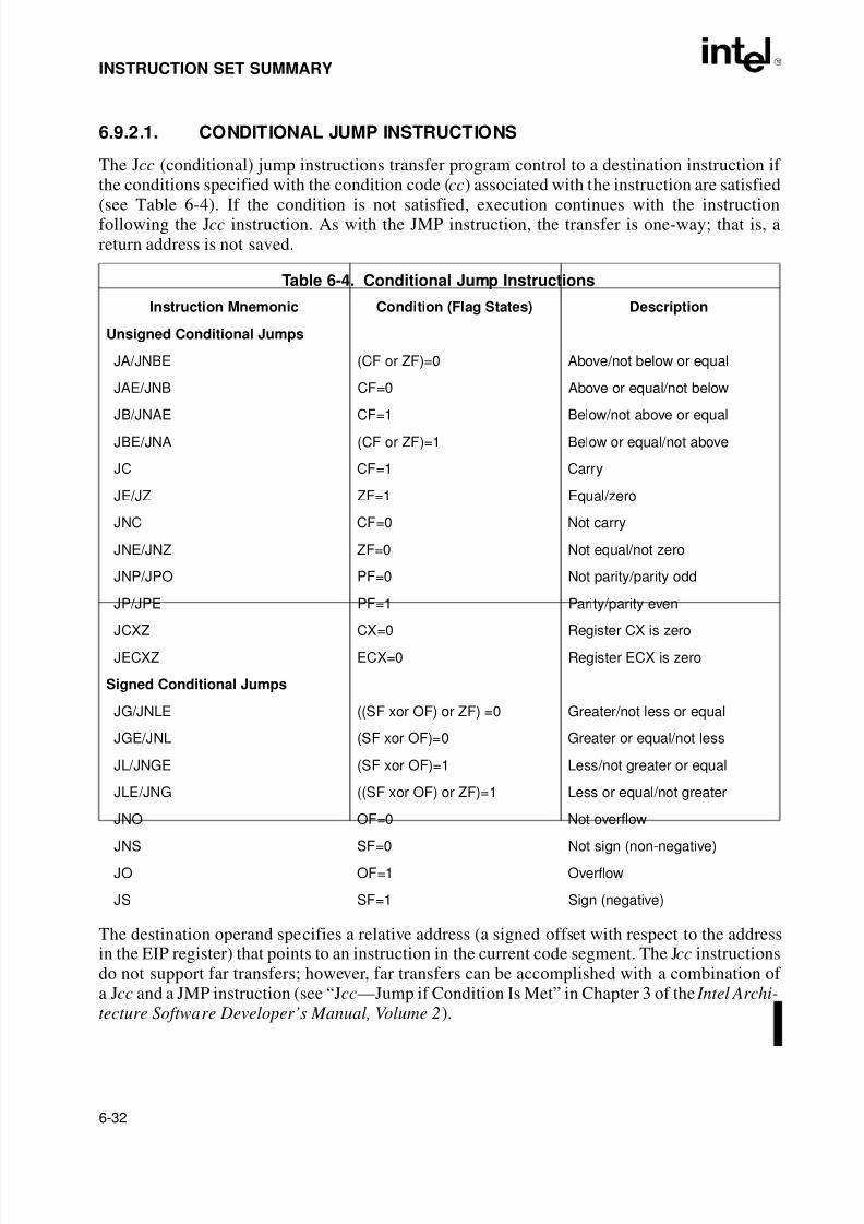
8/3/2019 Intel Architecture Software Developer's Manual, Volume 1: Basic Architecture
http://slidepdf.com/reader/full/intel-architecture-software-developers-manual-volume-1-basic-architecture 126/283
6-32
INSTRUCTION SET SUMMARY
6.9.2.1. CONDITIONAL JUMP INSTRUCTIONS
The Jcc (conditional) jump instructions transfer program control to a destination instruction if the conditions specified with the condition code (cc) associated with the instruction are satisfied
(see Table 6-4). If the condition is not satisfied, execution continues with the instructionfollowing the Jcc instruction. As with the JMP instruction, the transfer is one-way; that is, areturn address is not saved.
The destination operand specifies a relative address (a signed offset with respect to the addressin the EIP register) that points to an instruction in the current code segment. The Jcc instructionsdo not support far transfers; however, far transfers can be accomplished with a combination of a Jcc and a JMP instruction (see “Jcc—Jump if Condition Is Met” in Chapter 3 of the Intel Archi-
tecture Software Developer’s Manual, Volume 2).
Table 6-4. Conditional Jump Instructions
Instruction Mnemonic Condition (Flag States) Description
Unsigned Conditional Jumps
JA/JNBE (CF or ZF)=0 Above/not below or equal
JAE/JNB CF=0 Above or equal/not below
JB/JNAE CF=1 Below/not above or equalJBE/JNA (CF or ZF)=1 Below or equal/not above
JC CF=1 Carry
JE/JZ ZF=1 Equal/zero
JNC CF=0 Not carry
JNE/JNZ ZF=0 Not equal/not zero
JNP/JPO PF=0 Not parity/parity odd
JP/JPE PF=1 Parity/parity even
JCXZ CX=0 Register CX is zero
JECXZ ECX=0 Register ECX is zero
Signed Conditional Jumps
JG/JNLE ((SF xor OF) or ZF) =0 Greater/not less or equal
JGE/JNL (SF xor OF)=0 Greater or equal/not less
JL/JNGE (SF xor OF)=1 Less/not greater or equal
JLE/JNG ((SF xor OF) or ZF)=1 Less or equal/not greater
JNO OF=0 Not overflow
JNS SF=0 Not sign (non-negative)
JO OF=1 Overflow
JS SF=1 Sign (negative)
8/3/2019 Intel Architecture Software Developer's Manual, Volume 1: Basic Architecture
http://slidepdf.com/reader/full/intel-architecture-software-developers-manual-volume-1-basic-architecture 127/283
6-33
INSTRUCTION SET SUMMARY
Table 6-4 shows the mnemonics for the Jcc instructions and the conditions being tested for eachinstruction. The condition code mnemonics are appended to the letter “J” to form the mnemonicfor a Jcc instruction. The instructions are divided into two groups: unsigned and signed condi-tional jumps. These groups correspond to the results of operations performed on unsigned and
signed integers, respectively. Those instructions listed as pairs (for example, JA/JNBE) are alter-nate names for the same instruction. The assembler provides these alternate names to make iteasier to read program listings.
The JCXZ and JECXZ instructions test the CX and ECX registers, respectively, instead of oneor more status flags. See Section 6.9.2.3., “Jump If Zero Instructions” for more informationabout these instructions.
6.9.2.2. LOOP INSTRUCTIONS
The LOOP, LOOPE (loop while equal), LOOPZ (loop while zero), LOOPNE (loop while not
equal), and LOOPNZ (loop while not zero) instructions are conditional jump instructions thatuse the value of the ECX register as a count for the number of times to execute a loop. All theloop instructions decrement the count in the ECX register each time they are executed and termi-nate a loop when zero is reached. The LOOPE, LOOPZ, LOOPNE, and LOOPNZ instructionsalso accept the ZF flag as a condition for terminating the loop before the count reaches zero.
The LOOP instruction decrements the contents of the ECX register (or the CX register, if theaddress-size attribute is 16), then tests the register for the loop-termination condition. If thecount in the ECX register is non-zero, program control is transferred to the instruction addressspecified by the destination operand. The destination operand is a relative address (that is, anoffset relative to the contents of the EIP register), and it generally points to the first instruction
in the block of code that is to be executed in the loop. When the count in the ECX registerreaches zero, program control is transferred to the instruction immediately following theLOOP instruction, which terminates the loop. If the count in the ECX register is zero when theLOOP instruction is first executed, the register is pre-decremented to FFFFFFFFH, causing theloop to be executed 232 times.
The LOOPE and LOOPZ instructions perform the same operation (they are mnemonics for thesame instruction). These instructions operate the same as the LOOP instruction, except that theyalso test the ZF flag. If the count in the ECX register is not zero and the ZF flag is set, programcontrol is transferred to the destination operand. When the count reaches zero or the ZF flag isclear, the loop is terminated by transferring program control to the instruction immediately
following the LOOPE/LOOPZ instruction.
The LOOPNE and LOOPNZ instructions (mnemonics for the same instruction) operate thesame as the LOOPE/LOOPPZ instructions, except that they terminate the loop if the ZF flagis set.
6.9.2.3. JUMP IF ZERO INSTRUCTIONS
The JECXZ (jump if ECX zero) instruction jumps to the location specified in the destinationoperand if the ECX register contains the value zero. This instruction can be used in combinationwith a loop instruction (LOOP, LOOPE, LOOPZ, LOOPNE, or LOOPNZ) to test the ECXregister prior to beginning a loop. As described in Section 6.9.2.2., “Loop Instructions”, the loop
8/3/2019 Intel Architecture Software Developer's Manual, Volume 1: Basic Architecture
http://slidepdf.com/reader/full/intel-architecture-software-developers-manual-volume-1-basic-architecture 128/283
6-34
INSTRUCTION SET SUMMARY
instructions decrement the contents of the ECX register before testing for zero. If the value inthe ECX register is zero initially, it will be decremented to FFFFFFFFH on the first loop instruc-tion, causing the loop to be executed 232 times. To prevent this problem, a JECXZ instructioncan be inserted at the beginning of the code block for the loop, causing a jump out the loop if the
EAX register count is initially zero. When used with repeated string scan and compare instruc-tions, the JECXZ instruction can determine whether the loop terminated because the countreached zero or because the scan or compare conditions were satisfied.
The JCXZ (jump if CX is zero) instruction operates the same as the JECXZ instruction when the16-bit address-size attribute is used. Here, the CX register is tested for zero.
6.9.3. Software Interrupts
The INT n (software interrupt), INTO (interrupt on overflow), and BOUND (detect value out of
range) instructions allow a program to explicitly raise a specified interrupt or exception, whichin turn causes the handler routine for the interrupt or exception to be called.
The INT n instruction can raise any of the processor’s interrupts or exceptions by encoding thevector number or the interrupt or exception in the instruction. This instruction can be used tosupport software generated interrupts or to test the operation of interrupt and exception handlers.The IRET instruction (see Section 6.9.1.3., “Return From Interrupt Instruction”) allows returnsfrom interrupt handling routines.
The INTO instruction raises the overflow exception, if the OF flag is set. If the flag is clear,execution continues without raising the exception. This instruction allows software to access theoverflow exception handler explicitly to check for overflow conditions.
The BOUND instruction compares a signed value against upper and lower bounds, and raisesthe “BOUND range exceeded” exception if the value is less than the lower bound or greater thanthe upper bound. This instruction is useful for operations such as checking an array index tomake sure it falls within the range defined for the array.
6.10. STRING OPERATIONS
The MOVS (Move String), CMPS (Compare string), SCAS (Scan string), LODS (Load string),and STOS (Store string) instructions permit large data structures, such as alphanumeric char-acter strings, to be moved and examined in memory. These instructions operate on individualelements in a string, which can be a byte, word, or doubleword. The string elements to be oper-ated on are identified with the ESI (source string element) and EDI (destination string element)registers. Both of these registers contain absolute addresses (offsets into a segment) that point toa string element.
By default, the ESI register addresses the segment identified with the DS segment register. Asegment-override prefix allows the ESI register to be associated with the CS, SS, ES, FS, or GSsegment register. The EDI register addresses the segment identified with the ES segmentregister; no segment override is allowed for the EDI register. The use of two different segmentregisters in the string instructions permits operations to be performed on strings located indifferent segments. Or by associating the ESI register with the ES segment register, both the
8/3/2019 Intel Architecture Software Developer's Manual, Volume 1: Basic Architecture
http://slidepdf.com/reader/full/intel-architecture-software-developers-manual-volume-1-basic-architecture 129/283
6-35
INSTRUCTION SET SUMMARY
source and destination strings can be located in the same segment. (This latter condition can alsobe achieved by loading the DS and ES segment registers with the same segment selector andallowing the ESI register to default to the DS register.)
The MOVS instruction moves the string element addressed by the ESI register to the locationaddressed by the EDI register. The assembler recognizes three “short forms” of this instruction,which specify the size of the string to be moved: MOVSB (move byte string), MOVSW (moveword string), and MOVSD (move doubleword string).
The CMPS instruction subtracts the destination string element from the source string elementand updates the status flags (CF, ZF, OF, SF, PF, and AF) in the EFLAGS register according tothe results. Neither string element is written back to memory. The assembler recognizes three“short forms” of the CMPS instruction: CMPSB (compare byte strings), CMPSW (compareword strings), and CMPSD (compare doubleword strings).
The SCAS instruction subtracts the destination string element from the contents of the EAX,
AX, or AL register (depending on operand length) and updates the status flags according to theresults. The string element and register contents are not modified. The following “short forms”of the SCAS instruction specifies the operand length: SCASB (scan byte string), SCASW (scanword string), and SCASD (scan doubleword string).
The LODS instruction loads the source string element identified by the ESI register into theEAX register (for a doubleword string), the AX register (for a word string), or the AL register(for a byte string). The “short forms” for this instruction are LODSB (load byte string), LODSW(load word string), and LODSD (load doubleword string). This instruction is usually used in aloop, where other instructions process each element of the string after they are loaded into thetarget register.
The STOS instruction stores the source string element from the EAX (doubleword string), AX(word string), or AL (byte string) register into the memory location identified with the EDIregister. The “short forms” for this instruction are STOSB (store byte string), STOSW (storeword string), and STOSD (store doubleword string). This instruction is also normally used in aloop. Here a string is commonly loaded into the register with a LODS instruction, operatedon by other instructions, and then stored again in memory with a STOS instruction.
The I/O instructions (see Section 6.11., “I/O Instructions”) also perform operations on strings inmemory.
6.10.1. Repeating String Operations
The string instructions described in Section 6.10., “String Operations” perform one iteration of a string operation. To operate strings longer than a doubleword, the string instructions can becombined with a repeat prefix (REP) to create a repeating instruction or be placed in a loop.
When used in string instructions, the ESI and EDI registers are automatically incremented ordecremented after each iteration of an instruction to point to the next element (byte, word, ordoubleword) in the string. String operations can thus begin at higher addresses and work towardlower ones, or they can begin at lower addresses and work toward higher ones. The DF flag in

8/3/2019 Intel Architecture Software Developer's Manual, Volume 1: Basic Architecture
http://slidepdf.com/reader/full/intel-architecture-software-developers-manual-volume-1-basic-architecture 130/283
6-36
INSTRUCTION SET SUMMARY
the EFLAGS register controls whether the registers are incremented (DF=0) or decremented(DF=1). The STD and CLD instructions set and clear this flag, respectively.
The following repeat prefixes can be used in conjunction with a count in the ECX register to
cause a string instruction to repeat:• REP—Repeat while the ECX register not zero.
• REPE/REPZ—Repeat while the ECX register not zero and the ZF flag is set.
• REPNE/REPNZ—Repeat while the ECX register not zero and the ZF flag is clear.
When a string instruction has a repeat prefix, the operation executes until one of the terminationconditions specified by the prefix is satisfied. The REPE/REPZ and REPNE/REPNZ prefixesare used only with the CMPS and SCAS instructions. Also, note that a A REP STOS instructionis the fastest way to initialize a large block of memory.
6.11. I/O INSTRUCTIONS
The IN (input from port to register), INS (input from port to string), OUT (output from registerto port), and OUTS (output string to port) instructions move data between the processor’s I/Oports and either a register or memory.
The register I/O instructions (IN and OUT) move data between an I/O port and the EAX register(32-bit I/O), the AX register (16-bit I/O), or the AL (8-bit I/O) register. The I/O port being reador written to is specified with an immediate operand or an address in the DX register.
The block I/O instructions (INS and OUTS) instructions move blocks of data (strings) betweenan I/O port and memory. These instructions operate similar to the string instructions (see Section6.10., “String Operations”). The ESI and EDI registers are used to specify string elements inmemory and the repeat prefixes (REP) are used to repeat the instructions to implement block moves. The assembler recognizes the following alternate mnemonics for these instructions:INSB (input byte), INSW (input word), and INSD (input doubleword), and OUTB (output byte),OUTW (output word), and OUTD (output doubleword).
The INS and OUTS instructions use an address in the DX register to specify the I/O port to beread or written to.
6.12. ENTER AND LEAVE INSTRUCTIONS
The ENTER and LEAVE instructions provide machine-language support for procedure calls inblock-structured languages, such as C and Pascal. These instructions and the call and returnmechanism that they support are described in detail in Section 4.5., “Procedure Calls for Block-Structured Languages”.
8/3/2019 Intel Architecture Software Developer's Manual, Volume 1: Basic Architecture
http://slidepdf.com/reader/full/intel-architecture-software-developers-manual-volume-1-basic-architecture 131/283
6-37
INSTRUCTION SET SUMMARY
6.13. EFLAGS INSTRUCTIONS
The EFLAGS instructions allow the state of selected flags in the EFLAGS register to be read ormodified.
6.13.1. Carry and Direction Flag Instructions
The STC (set carry flag), CLC (clear carry flag), and CMC (complement carry flag) instructionsallow the CF flags in the EFLAGS register to be modified directly. They are typically used toinitialize the CF flag to a known state before an instruction that uses the flag in an operation isexecuted. They are also used in conjunction with the rotate-with-carry instructions (RCL andRCR).
The STD (set direction flag) and CLD (clear direction flag) instructions allow the DF flag in the
EFLAGS register to be modified directly. The DF flag determines the direction in which indexregisters ESI and EDI are stepped when executing string processing instructions. If the DF flagis clear, the index registers are incremented after each iteration of a string instruction; if the DFflag is set, the registers are decremented.
6.13.2. Interrupt Flag Instructions
The STI (set interrupt flag) and CTI (clear interrupt flag) instructions allow the interrupt IF flagin the EFLAGS register to be modified directly. The IF flag controls the servicing of hardware-generated interrupts (those received at the processor’s INTR pin). If the IF flag is set, the
processor services hardware interrupts; if the IF flag is clear, hardware interrupts are masked.
6.13.3. EFLAGS Transfer Instructions
The EFLAGS transfer instructions allow groups of flags in the EFLAGS register to be copied toa register or memory or be loaded from a register or memory.
The LAHF (load AH from flags) and SAHF (store AH into flags) instructions operate on five of the EFLAGS status flags (SF, ZF, AF, PF, and CF). The LAHF instruction copies the status flagsto bits 7, 6, 4, 2, and 0 of the AH register, respectively. The contents of the remaining bits in the
register (bits 5, 3, and 1) are undefined, and the contents of the EFLAGS register remainunchanged. The SAHF instruction copies bits 7, 6, 4, 2, and 0 from the AH register into the SF,ZF, AF, PF, and CF flags, respectively in the EFLAGS register.
The PUSHF (push flags), PUSHFD (push flags double), POPF (pop flags), and POPFD (popflags double) instructions copy the flags in the EFLAGS register to and from the stack. ThePUSHF instruction pushes the lower word of the EFLAGS register onto the stack (see Figure6-11). The PUSHFD instruction pushes the entire EFLAGS register onto the stack (with the RFand VM flags read as clear).
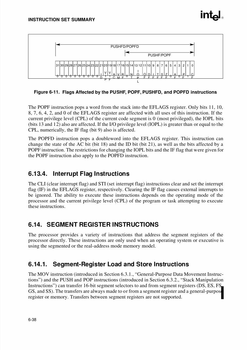
8/3/2019 Intel Architecture Software Developer's Manual, Volume 1: Basic Architecture
http://slidepdf.com/reader/full/intel-architecture-software-developers-manual-volume-1-basic-architecture 132/283
6-38
INSTRUCTION SET SUMMARY
The POPF instruction pops a word from the stack into the EFLAGS register. Only bits 11, 10,8, 7, 6, 4, 2, and 0 of the EFLAGS register are affected with all uses of this instruction. If the
current privilege level (CPL) of the current code segment is 0 (most privileged), the IOPL bits(bits 13 and 12) also are affected. If the I/O privilege level (IOPL) is greater than or equal to theCPL, numerically, the IF flag (bit 9) also is affected.
The POPFD instruction pops a doubleword into the EFLAGS register. This instruction canchange the state of the AC bit (bit 18) and the ID bit (bit 21), as well as the bits affected by aPOPF instruction. The restrictions for changing the IOPL bits and the IF flag that were given forthe POPF instruction also apply to the POPFD instruction.
6.13.4. Interrupt Flag Instructions
The CLI (clear interrupt flag) and STI (set interrupt flag) instructions clear and set the interruptflag (IF) in the EFLAGS register, respectively. Clearing the IF flag causes external interrupts tobe ignored. The ability to execute these instructions depends on the operating mode of theprocessor and the current privilege level (CPL) of the program or task attempting to executethese instructions.
6.14. SEGMENT REGISTER INSTRUCTIONS
The processor provides a variety of instructions that address the segment registers of the
processor directly. These instructions are only used when an operating system or executive isusing the segmented or the real-address mode memory model.
6.14.1. Segment-Register Load and Store Instructions
The MOV instruction (introduced in Section 6.3.1., “General-Purpose Data Movement Instruc-tions”) and the PUSH and POP instructions (introduced in Section 6.3.2., “Stack ManipulationInstructions”) can transfer 16-bit segment selectors to and from segment registers (DS, ES, FS,GS, and SS). The transfers are always made to or from a segment register and a general-purposeregister or memory. Transfers between segment registers are not supported.
Figure 6-11. Flags Affected by the PUSHF, POPF, PUSHFD, and POPFD instructions
PUSHFD/POPFD
PUSHF/POPF
31 2930 28 27 26 25 24 23 22 2120 19 18 17 16
0RF
ID
AC
VM
15 1314 12 11 10 9 8 7 6 5 4 3 2 1 0
0CF
AF
PF 1
DF
IF
TF
SF
ZF
NT 000 0 0 0 0 0 0 0 0
VIP
VIF
OF
IOPL

8/3/2019 Intel Architecture Software Developer's Manual, Volume 1: Basic Architecture
http://slidepdf.com/reader/full/intel-architecture-software-developers-manual-volume-1-basic-architecture 133/283
6-39
INSTRUCTION SET SUMMARY
The POP and MOV instructions cannot place a value in the CS register. Only the far control-transfer versions of the JMP, CALL, and RET instructions (see Section 6.14.2., “Far ControlTransfer Instructions”) affect the CS register directly.
6.14.2. Far Control Transfer Instructions
The JMP and CALL instructions (see Section 6.9., “Control Transfer Instructions”) both accepta far pointer as a source operand to transfer program control to a segment other than the segmentcurrently being pointed to by the CS register. When a far call is made with the CALL instruction,the current values of the EIP and CS registers are both pushed on the stack.
The RET instruction (see Section 6.9.1.2., “Call and Return Instructions”) can be used toexecute a far return. Here, program control is transferred from a code segment that contains acalled procedure back to the code segment that contained the calling procedure. The RET
instruction restores the values of the CS and EIP registers for the calling procedure from thestack.
6.14.3. Software Interrupt Instructions
The software interrupt instructions INT, INTO, BOUND, and IRET (see Section 6.9.3., “Soft-ware Interrupts”) can also call and return from interrupt and exception handler procedures thatare located in a code segment other than the current code segment. With these instructions,however, the switching of code segments is handled transparently from the application program.
6.14.4. Load Far Pointer Instructions
The load far pointer instructions LDS (load far pointer using DS), LES (load far pointer usingES), LFS (load far pointer using FS), LGS (load far pointer using GS), and LSS (load far pointerusing SS) load a far pointer from memory into a segment register and a general-purpose generalregister. The segment selector part of the far pointer is loaded into the selected segment registerand the offset is loaded into the selected general-purpose register.
6.15. MISCELLANEOUS INSTRUCTIONSThe following instructions perform miscellaneous operations that are of interest to applicationsprogrammers.
6.15.1. Address Computation Instruction
The LEA (load effective address) instruction computes the effective address in memory (offsetwithin a segment) of a source operand and places it in a general-purpose register. This instruc-tion can interpret any of the Pentium Pro processor’s addressing modes and can perform any
indexing or scaling that may be needed. It is especially useful for initializing the ESI or EDI
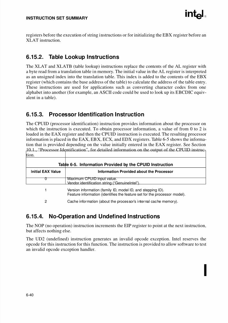
8/3/2019 Intel Architecture Software Developer's Manual, Volume 1: Basic Architecture
http://slidepdf.com/reader/full/intel-architecture-software-developers-manual-volume-1-basic-architecture 134/283
6-40
INSTRUCTION SET SUMMARY
registers before the execution of string instructions or for initializing the EBX register before anXLAT instruction.
6.15.2. Table Lookup Instructions
The XLAT and XLATB (table lookup) instructions replace the contents of the AL register witha byte read from a translation table in memory. The initial value in the AL register is interpretedas an unsigned index into the translation table. This index is added to the contents of the EBXregister (which contains the base address of the table) to calculate the address of the table entry.These instructions are used for applications such as converting character codes from onealphabet into another (for example, an ASCII code could be used to look up its EBCDIC equiv-alent in a table).
6.15.3. Processor Identification Instruction
The CPUID (processor identification) instruction provides information about the processor onwhich the instruction is executed. To obtain processor information, a value of from 0 to 2 isloaded in the EAX register and then the CPUID instruction is executed. The resulting processorinformation is placed in the EAX, EBX, ECX, and EDX registers. Table 6-5 shows the informa-tion that is provided depending on the value initially entered in the EAX register. See Section10.1., “Processor Identification”, for detailed information on the output of the CPUID instruc-tion.
6.15.4. No-Operation and Undefined Instructions
The NOP (no operation) instruction increments the EIP register to point at the next instruction,but affects nothing else.
The UD2 (undefined) instruction generates an invalid opcode exception. Intel reserves theopcode for this instruction for this function. The instruction is provided to allow software to testan invalid opcode exception handler.
Table 6-5. Information Provided by the CPUID InstructionInitial EAX Value Information Provided about the Processor
0 Maximum CPUID input value.Vendor identification string (“GenuineIntel”).
1 Version information (family ID, model ID, and stepping ID).Feature information (identifies the feature set for the processor model).
2 Cache information (about the processor’s internal cache memory).

8/3/2019 Intel Architecture Software Developer's Manual, Volume 1: Basic Architecture
http://slidepdf.com/reader/full/intel-architecture-software-developers-manual-volume-1-basic-architecture 135/283
7Floating-Point Unit

8/3/2019 Intel Architecture Software Developer's Manual, Volume 1: Basic Architecture
http://slidepdf.com/reader/full/intel-architecture-software-developers-manual-volume-1-basic-architecture 136/283
8/3/2019 Intel Architecture Software Developer's Manual, Volume 1: Basic Architecture
http://slidepdf.com/reader/full/intel-architecture-software-developers-manual-volume-1-basic-architecture 137/283
7-1
CHAPTER 7FLOATING-POINT UNIT
The Intel Architecture Floating-Point Unit (FPU) provides high-performance floating-pointprocessing capabilities. It supports the real, integer, and BCD-integer data types and the floating-point processing algorithms and exception handling architecture defined in the IEEE 754 and854 Standards for Floating-Point Arithmetic. The FPU executes instructions from theprocessor’s normal instruction stream and greatly improves the efficiency of Intel Architectureprocessors in handling the types of high-precision floating-point processing operationscommonly found in scientific, engineering, and business applications.
This chapter describes the data types that the FPU operates on, the FPU’s execution environ-ment, and the FPU-specific instruction set. Detailed descriptions of the FPU instructions aregiven in Chapter 3, Instruction Set Reference, in the Intel Architecture Software Developer’s
Manual, Volume 2.
7.1. COMPATIBILITY AND EASE OF USE OF THE INTELARCHITECTURE FPU
The architecture of the Intel Architecture FPU has evolved in parallel with the architecture of early Intel Architecture processors. The first Intel Math Coprocessors (the Intel 8087, Intel 287,
and Intel 387) were companion processors to the Intel 8086/8088, Intel 286, and Intel386processors, respectively, and were designed to improve and extend the numeric processing capa-bility of the Intel Architecture. The Intel486 DX processor for the first time integrated the CPUand the FPU architectures on one chip. The Pentium processor’s FPU offered the same architec-ture as the Intel486 DX processor’s FPU, but with improved performance. The Pentium Proprocessor’s FPU further extended the floating-point processing capability of Intel Architecturefamily of processors and added several new instructions to improve processing throughput.
Throughout this evolution, compatibility among the various generations of FPUs and mathcoprocessors has been maintained. For example, the Pentium Pro processor’s FPU is fullycompatible with the Pentium and Intel486 DX processors’s FPUs.
Each generation of the Intel Architecture FPUs have been explicitly designed to deliver stable,accurate results when programmed using straightforward “pencil and paper” algorithms,bringing the functionality and power of accurate numeric computation into the hands of thegeneral user. The IEEE 754 standard specifically addresses this issue, recognizing the funda-mental importance of making numeric computations both easy and safe to use.
For example, some processors can overflow when two single-precision floating-point numbersare multiplied together and then divided by a third, even if the final result is a perfectly valid 32-bit number. The Intel Architecture FPUs deliver the correctly rounded result. Other typicalexamples of undesirable machine behavior in straightforward calculations occur whencomputing financial rate of return, which involves the expression (1 + i)n or when solving forroots of a quadratic equation:
8/3/2019 Intel Architecture Software Developer's Manual, Volume 1: Basic Architecture
http://slidepdf.com/reader/full/intel-architecture-software-developers-manual-volume-1-basic-architecture 138/283
7-2
FLOATING-POINT UNIT
If a does not equal 0, the formula is numerically unstable when the roots are nearly coincidentor when their magnitudes are wildly different. The formula is also vulnerable to spuriousover/underflows when the coefficients a, b, and c are all very big or all very tiny. When single-precision (4-byte) floating-point coefficients are given as data and the formula is evaluated in theFPU's normal way, keeping all intermediate results in its stack, the FPU produces impeccablesingle-precision roots. This happens because, by default and with no effort on the programmer'spart, the FPU evaluates all those sub-expressions with so much extra precision and range as tooverwhelm almost any threat to numerical integrity.
If double-precision data and results were at issue, a better formula would have to be used, and
once again the FPU's default evaluation of that formula would provide substantially enhancednumerical integrity over mere double-precision evaluation.
On most machines, straightforward algorithms will not deliver consistently correct results (andwill not indicate when they are incorrect). To obtain correct results on traditional machines underall conditions usually requires sophisticated numerical techniques that go beyond typicalprogramming practice. General application programmers using straightforward algorithms willproduce much more reliable programs using the Intel architectures. This simple fact greatlyreduces the software investment required to develop safe, accurate computation-based products.
Beyond traditional numeric support for scientific applications, the Intel architectures have built-
in facilities for commercial computing. They can process decimal numbers of up to 18 digitswithout round-off errors, performing exact arithmetic on integers as large as 264 (or 1018).Exact arithmetic is vital in accounting applications where rounding errors may introduce mone-tary losses that cannot be reconciled.
The Intel FPU's contain a number of optional numerical facilities that can be invoked by sophis-ticated users. These advanced features include directed rounding, gradual underflow, andprogrammed exception-handling facilities.
These automatic exception-handling facilities permit a high degree of flexibility in numericprocessing software, without burdening the programmer. While performing numeric calcula-tions, the processor automatically detects exception conditions that can potentially damage a
calculation (for example, X ÷ 0 or when X < 0). By default, on-chip exception logic handlesthese exceptions so that a reasonable result is produced and execution may proceed withoutprogram interruption. Alternatively, the processor can invoke a software exception handler toprovide special results whenever various types of exceptions are detected.
7.2. REAL NUMBERS AND FLOATING-POINT FORMATS
This section describes how real numbers are represented in floating-point format in the IntelArchitecture FPU. It also introduces terms such as normalized numbers, denormalized numbers,biased exponents, signed zeros, and NaNs. Readers who are already familiar with floating-pointprocessing techniques and the IEEE standards may wish to skip this section.
b– b2
4ac–±
2a
---------------------------------------
X
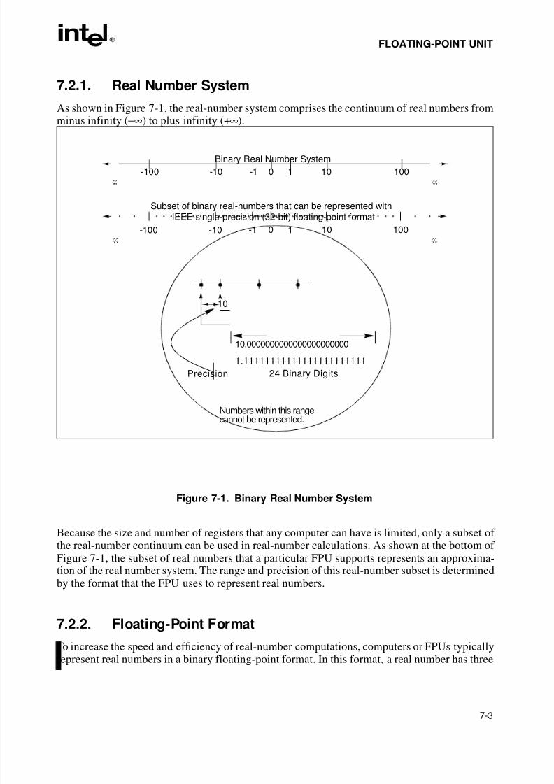
8/3/2019 Intel Architecture Software Developer's Manual, Volume 1: Basic Architecture
http://slidepdf.com/reader/full/intel-architecture-software-developers-manual-volume-1-basic-architecture 139/283
7-3
FLOATING-POINT UNIT
7.2.1. Real Number System
As shown in Figure 7-1, the real-number system comprises the continuum of real numbers fromminus infinity (−∞) to plus infinity (+∞).
Because the size and number of registers that any computer can have is limited, only a subset of the real-number continuum can be used in real-number calculations. As shown at the bottom of Figure 7-1, the subset of real numbers that a particular FPU supports represents an approxima-tion of the real number system. The range and precision of this real-number subset is determinedby the format that the FPU uses to represent real numbers.
7.2.2. Floating-Point Format
To increase the speed and efficiency of real-number computations, computers or FPUs typicallyrepresent real numbers in a binary floating-point format. In this format, a real number has three
Figure 7-1. Binary Real Number System
Binary Real Number System
Subset of binary real-numbers that can be represented withIEEE single-precision (32-bit) floating-point format
+10
10.0000000000000000000000
1.11111111111111111111111
Precision 24 Binary Digits
Numbers within this rangecannot be represented.
ςς ςς
-100 -10 -1 0 1 10 100
ςς ςς
-100 -10 -1 0 1 10 100
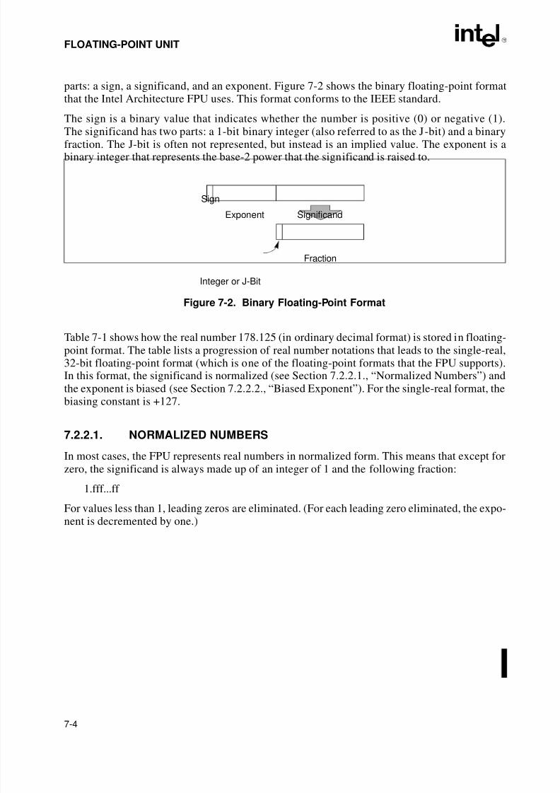
8/3/2019 Intel Architecture Software Developer's Manual, Volume 1: Basic Architecture
http://slidepdf.com/reader/full/intel-architecture-software-developers-manual-volume-1-basic-architecture 140/283
7-4
FLOATING-POINT UNIT
parts: a sign, a significand, and an exponent. Figure 7-2 shows the binary floating-point formatthat the Intel Architecture FPU uses. This format conforms to the IEEE standard.
The sign is a binary value that indicates whether the number is positive (0) or negative (1).
The significand has two parts: a 1-bit binary integer (also referred to as the J-bit) and a binaryfraction. The J-bit is often not represented, but instead is an implied value. The exponent is abinary integer that represents the base-2 power that the significand is raised to.
Table 7-1 shows how the real number 178.125 (in ordinary decimal format) is stored in floating-point format. The table lists a progression of real number notations that leads to the single-real,32-bit floating-point format (which is one of the floating-point formats that the FPU supports).In this format, the significand is normalized (see Section 7.2.2.1., “Normalized Numbers”) andthe exponent is biased (see Section 7.2.2.2., “Biased Exponent”). For the single-real format, thebiasing constant is +127.
7.2.2.1. NORMALIZED NUMBERS
In most cases, the FPU represents real numbers in normalized form. This means that except forzero, the significand is always made up of an integer of 1 and the following fraction:
1.fff...ff
For values less than 1, leading zeros are eliminated. (For each leading zero eliminated, the expo-nent is decremented by one.)
Figure 7-2. Binary Floating-Point Format
Sign
Integer or J-Bit
Exponent Significand
Fraction
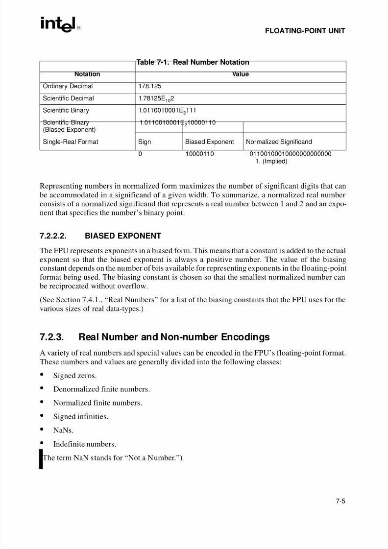
8/3/2019 Intel Architecture Software Developer's Manual, Volume 1: Basic Architecture
http://slidepdf.com/reader/full/intel-architecture-software-developers-manual-volume-1-basic-architecture 141/283
7-5
FLOATING-POINT UNIT
Representing numbers in normalized form maximizes the number of significant digits that canbe accommodated in a significand of a given width. To summarize, a normalized real numberconsists of a normalized significand that represents a real number between 1 and 2 and an expo-nent that specifies the number’s binary point.
7.2.2.2. BIASED EXPONENT
The FPU represents exponents in a biased form. This means that a constant is added to the actualexponent so that the biased exponent is always a positive number. The value of the biasingconstant depends on the number of bits available for representing exponents in the floating-pointformat being used. The biasing constant is chosen so that the smallest normalized number canbe reciprocated without overflow.
(See Section 7.4.1., “Real Numbers” for a list of the biasing constants that the FPU uses for thevarious sizes of real data-types.)
7.2.3. Real Number and Non-number Encodings
A variety of real numbers and special values can be encoded in the FPU’s floating-point format.These numbers and values are generally divided into the following classes:
• Signed zeros.
• Denormalized finite numbers.
• Normalized finite numbers.
• Signed infinities.
• NaNs.
• Indefinite numbers.
(The term NaN stands for “Not a Number.”)
Table 7-1. Real Number Notation
Notation Value
Ordinary Decimal 178.125
Scientific Decimal 1.78125E102
Scientific Binary 1.0110010001E2111
Scientific Binary(Biased Exponent)
1.0110010001E210000110
Single-Real Format Sign Biased Exponent Normalized Significand
0 10000110 011001000100000000000001. (Implied)
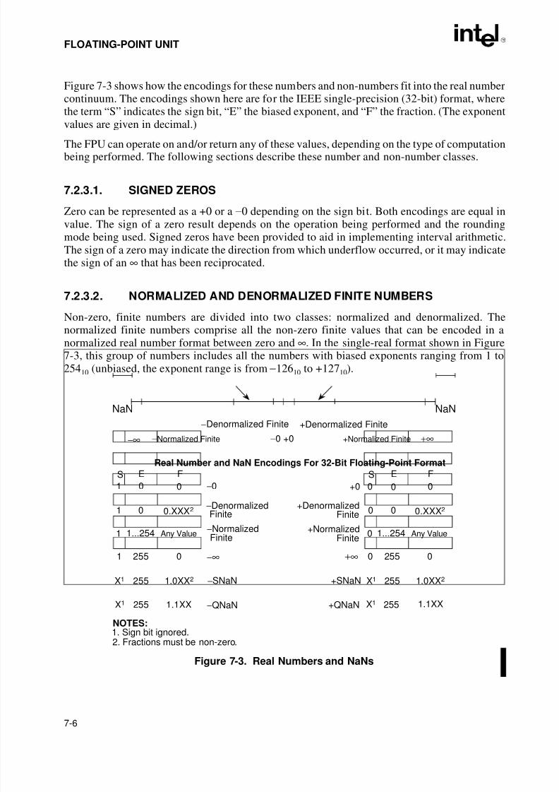
8/3/2019 Intel Architecture Software Developer's Manual, Volume 1: Basic Architecture
http://slidepdf.com/reader/full/intel-architecture-software-developers-manual-volume-1-basic-architecture 142/283
7-6
FLOATING-POINT UNIT
Figure 7-3 shows how the encodings for these numbers and non-numbers fit into the real numbercontinuum. The encodings shown here are for the IEEE single-precision (32-bit) format, wherethe term “S” indicates the sign bit, “E” the biased exponent, and “F” the fraction. (The exponentvalues are given in decimal.)
The FPU can operate on and/or return any of these values, depending on the type of computationbeing performed. The following sections describe these number and non-number classes.
7.2.3.1. SIGNED ZEROS
Zero can be represented as a +0 or a −0 depending on the sign bit. Both encodings are equal invalue. The sign of a zero result depends on the operation being performed and the roundingmode being used. Signed zeros have been provided to aid in implementing interval arithmetic.The sign of a zero may indicate the direction from which underflow occurred, or it may indicatethe sign of an ∞ that has been reciprocated.
7.2.3.2. NORMALIZED AND DENORMALIZED FINITE NUMBERS
Non-zero, finite numbers are divided into two classes: normalized and denormalized. Thenormalized finite numbers comprise all the non-zero finite values that can be encoded in anormalized real number format between zero and ∞. In the single-real format shown in Figure7-3, this group of numbers includes all the numbers with biased exponents ranging from 1 to25410 (unbiased, the exponent range is from −12610 to +12710).
Figure 7-3. Real Numbers and NaNs
1 0 0
S E F
−0
1 0−DenormalizedFinite
NaN
1 1...254 Any Value−NormalizedFinite
1 255 0 −∞
255 1.0XX2 −SNaN
255 1.1XX −QNaN
NOTES:1. Sign bit ignored.2. Fractions must be non-zero.
0 0 0
S E F
0 0
NaN
0 1...254 Any Value
0 255 0
X1 255 1.0XX2
255 1.1XX
+0
+DenormalizedFinite
+Normalized
Finite+∞
+SNaN
+QNaN X1
X1
X1
Real Number and NaN Encodings For 32-Bit Floating-Point Format
−Denormalized Finite
−Normalized Finite −0−∞ +∞
+Denormalized Finite
+Normalized Finite+0
0.XXX2 0.XXX2
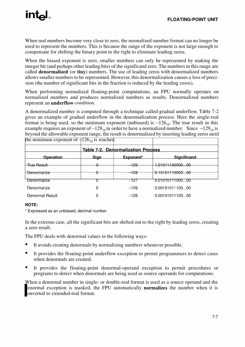
8/3/2019 Intel Architecture Software Developer's Manual, Volume 1: Basic Architecture
http://slidepdf.com/reader/full/intel-architecture-software-developers-manual-volume-1-basic-architecture 143/283
7-7
FLOATING-POINT UNIT
When real numbers become very close to zero, the normalized-number format can no longer beused to represent the numbers. This is because the range of the exponent is not large enough tocompensate for shifting the binary point to the right to eliminate leading zeros.
When the biased exponent is zero, smaller numbers can only be represented by making theinteger bit (and perhaps other leading bits) of the significand zero. The numbers in this range arecalled denormalized (or tiny) numbers. The use of leading zeros with denormalized numbersallows smaller numbers to be represented. However, this denormalization causes a loss of preci-sion (the number of significant bits in the fraction is reduced by the leading zeros).
When performing normalized floating-point computations, an FPU normally operates onnormalized numbers and produces normalized numbers as results. Denormalized numbersrepresent an underflow condition.
A denormalized number is computed through a technique called gradual underflow. Table 7-2
gives an example of gradual underflow in the denormalization process. Here the single-realformat is being used, so the minimum exponent (unbiased) is −12610. The true result in thisexample requires an exponent of −12910 in order to have a normalized number. Since −12910 isbeyond the allowable exponent range, the result is denormalized by inserting leading zeros untilthe minimum exponent of −12610 is reached.
NOTE:
* Expressed as an unbiased, decimal number.
In the extreme case, all the significant bits are shifted out to the right by leading zeros, creatinga zero result.
The FPU deals with denormal values in the following ways:• It avoids creating denormals by normalizing numbers whenever possible.
• It provides the floating-point underflow exception to permit programmers to detect caseswhen denormals are created.
• It provides the floating-point denormal-operand exception to permit procedures orprograms to detect when denormals are being used as source operands for computations.
When a denormal number in single- or double-real format is used as a source operand and thedenormal exception is masked, the FPU automatically normalizes the number when it isconverted to extended-real format.
Table 7-2. Denormalization Process
Operation Sign Exponent* Significand
True Result 0 −129 1.01011100000...00
Denormalize 0 −128 0.10101110000...00
Denormalize 0 −127 0.01010111000...00
Denormalize 0 −126 0.00101011100...00
Denormal Result 0 −126 0.00101011100...00
8/3/2019 Intel Architecture Software Developer's Manual, Volume 1: Basic Architecture
http://slidepdf.com/reader/full/intel-architecture-software-developers-manual-volume-1-basic-architecture 144/283
7-8
FLOATING-POINT UNIT
7.2.3.3. SIGNED INFINITIES
The two infinities, +∞ and −∞, represent the maximum positive and negative real numbers,respectively, that can be represented in the floating-point format. Infinity is always represented
by a zero significand (fraction and integer bit) and the maximum biased exponent allowed in thespecified format (for example, 25510 for the single-real format).
The signs of infinities are observed, and comparisons are possible. Infinities are always inter-preted in the affine sense; that is, –∞ is less than any finite number and +∞ is greater than anyfinite number. Arithmetic on infinities is always exact. Exceptions are generated only when theuse of an infinity as a source operand constitutes an invalid operation.
Whereas denormalized numbers represent an underflow condition, the two infinity numbersrepresent the result of an overflow condition. Here, the normalized result of a computation hasa biased exponent greater than the largest allowable exponent for the selected result format.
7.2.3.4. NANS
Since NaNs are non-numbers, they are not part of the real number line. In Figure 7-3, theencoding space for NaNs in the FPU floating-point formats is shown above the ends of the realnumber line. This space includes any value with the maximum allowable biased exponent and anon-zero fraction. (The sign bit is ignored for NaNs.)
The IEEE standard defines two classes of NaN: quiet NaNs (QNaNs) and signaling NaNs(SNaNs). A QNaN is a NaN with the most significant fraction bit set; an SNaN is a NaN withthe most significant fraction bit clear. QNaNs are allowed to propagate through most arithmeticoperations without signaling an exception. SNaNs generally signal an invalid-operation excep-tion whenever they appear as operands in arithmetic operations. Exceptions are discussed inSection 7.7., “Floating-Point Exception Handling”.
See Section 7.6., “Operating on NaNs”, for detailed information on how the FPU handles NaNs.
7.2.4. Indefinite
For each FPU data type, one unique encoding is reserved for representing the special value
indefinite. For example, when operating on real values, the real indefinite value is a QNaN(see Section 7.4.1., “Real Numbers”). The FPU produces indefinite values as responses tomasked floating-point exceptions.
7.3. FPU ARCHITECTURE
From an abstract, architectural view, the FPU is a coprocessor that operates in parallel with theprocessor’s integer unit (see Figure 7-4). The FPU gets its instructions from the same instructiondecoder and sequencer as the integer unit and shares the system bus with the integer unit. Otherthan these connections, the integer unit and FPU operate independently and in parallel. (Theactual microarchitecture of an Intel Architecture processor varies among the various families of
processors. For example, the Pentium Pro processor has two integer units and two FPUs;whereas, the Pentium processor has two integer units and one FPU, and the Intel486 processorhas one integer unit and one FPU.)
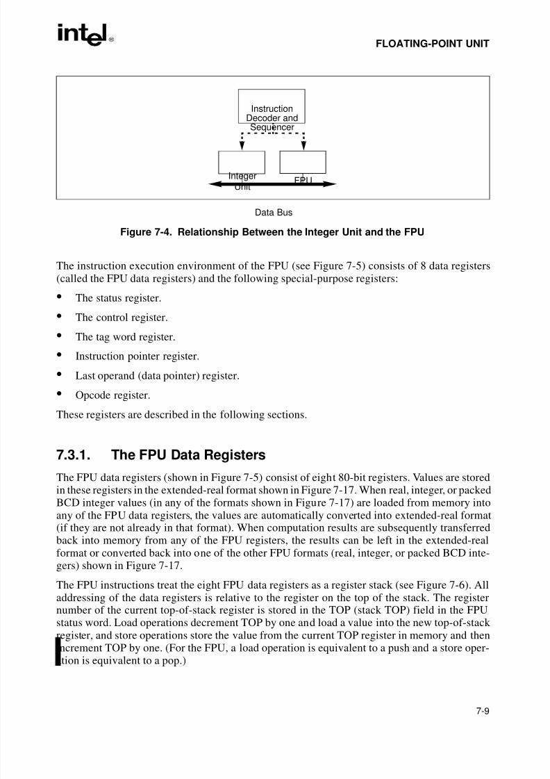
8/3/2019 Intel Architecture Software Developer's Manual, Volume 1: Basic Architecture
http://slidepdf.com/reader/full/intel-architecture-software-developers-manual-volume-1-basic-architecture 145/283
7-9
FLOATING-POINT UNIT
The instruction execution environment of the FPU (see Figure 7-5) consists of 8 data registers(called the FPU data registers) and the following special-purpose registers:
• The status register.
• The control register.
• The tag word register.
• Instruction pointer register.
• Last operand (data pointer) register.
• Opcode register.These registers are described in the following sections.
7.3.1. The FPU Data Registers
The FPU data registers (shown in Figure 7-5) consist of eight 80-bit registers. Values are storedin these registers in the extended-real format shown in Figure 7-17. When real, integer, or packedBCD integer values (in any of the formats shown in Figure 7-17) are loaded from memory intoany of the FPU data registers, the values are automatically converted into extended-real format(if they are not already in that format). When computation results are subsequently transferredback into memory from any of the FPU registers, the results can be left in the extended-realformat or converted back into one of the other FPU formats (real, integer, or packed BCD inte-gers) shown in Figure 7-17.
The FPU instructions treat the eight FPU data registers as a register stack (see Figure 7-6). Alladdressing of the data registers is relative to the register on the top of the stack. The registernumber of the current top-of-stack register is stored in the TOP (stack TOP) field in the FPUstatus word. Load operations decrement TOP by one and load a value into the new top-of-stack register, and store operations store the value from the current TOP register in memory and thenincrement TOP by one. (For the FPU, a load operation is equivalent to a push and a store oper-ation is equivalent to a pop.)
Figure 7-4. Relationship Between the Integer Unit and the FPU
Instruction
Data Bus
Decoder andSequencer
FPUInteger
Unit
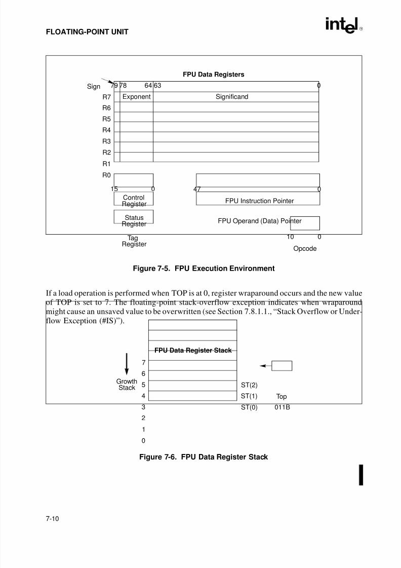
8/3/2019 Intel Architecture Software Developer's Manual, Volume 1: Basic Architecture
http://slidepdf.com/reader/full/intel-architecture-software-developers-manual-volume-1-basic-architecture 146/283
7-10
FLOATING-POINT UNIT
If a load operation is performed when TOP is at 0, register wraparound occurs and the new valueof TOP is set to 7. The floating-point stack-overflow exception indicates when wraparoundmight cause an unsaved value to be overwritten (see Section 7.8.1.1., “Stack Overflow or Under-flow Exception (#IS)”).
Figure 7-5. FPU Execution Environment
Figure 7-6. FPU Data Register Stack
079
R7R6
R5
R4
R3
R2
R1
R0
FPU Data Registers
Exponent Significand
78 64 63
15
ControlRegister
0
StatusRegister
TagRegister
047
FPU Instruction Pointer
FPU Operand (Data) Pointer
10
Opcode
0
Sign
7
6
5
4
3
2
1
0
FPU Data Register Stack
ST(2)
ST(1)
ST(0)
Top
011B
Growth
Stack
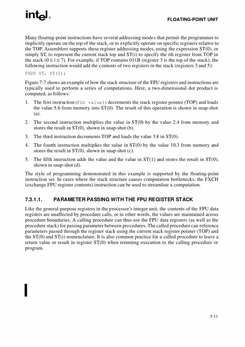
8/3/2019 Intel Architecture Software Developer's Manual, Volume 1: Basic Architecture
http://slidepdf.com/reader/full/intel-architecture-software-developers-manual-volume-1-basic-architecture 147/283
7-11
FLOATING-POINT UNIT
Many floating-point instructions have several addressing modes that permit the programmer toimplicitly operate on the top of the stack, or to explicitly operate on specific registers relative tothe TOP. Assemblers supports these register addressing modes, using the expression ST(0), orsimply ST, to represent the current stack top and ST(i) to specify the ith register from TOP in
the stack (0 ≤ i ≤ 7). For example, if TOP contains 011B (register 3 is the top of the stack), thefollowing instruction would add the contents of two registers in the stack (registers 3 and 5):
FADD ST, ST(2);
Figure 7-7 shows an example of how the stack structure of the FPU registers and instructions aretypically used to perform a series of computations. Here, a two-dimensional dot product iscomputed, as follows:
1. The first instruction (FLD value1) decrements the stack register pointer (TOP) and loadsthe value 5.6 from memory into ST(0). The result of this operation is shown in snap-shot(a).
2. The second instruction multiplies the value in ST(0) by the value 2.4 from memory andstores the result in ST(0), shown in snap-shot (b).
3. The third instruction decrements TOP and loads the value 3.8 in ST(0).
4. The fourth instruction multiplies the value in ST(0) by the value 10.3 from memory andstores the result in ST(0), shown in snap-shot (c).
5. The fifth instruction adds the value and the value in ST(1) and stores the result in ST(0),shown in snap-shot (d).
The style of programming demonstrated in this example is supported by the floating-point
instruction set. In cases where the stack structure causes computation bottlenecks, the FXCH(exchange FPU register contents) instruction can be used to streamline a computation.
7.3.1.1. PARAMETER PASSING WITH THE FPU REGISTER STACK
Like the general-purpose registers in the processor’s integer unit, the contents of the FPU dataregisters are unaffected by procedure calls, or in other words, the values are maintained acrossprocedure boundaries. A calling procedure can thus use the FPU data registers (as well as theprocedure stack) for passing parameter between procedures. The called procedure can referenceparameters passed through the register stack using the current stack register pointer (TOP) and
the ST(0) and ST(i) nomenclature. It is also common practice for a called procedure to leave areturn value or result in register ST(0) when returning execution to the calling procedure orprogram.
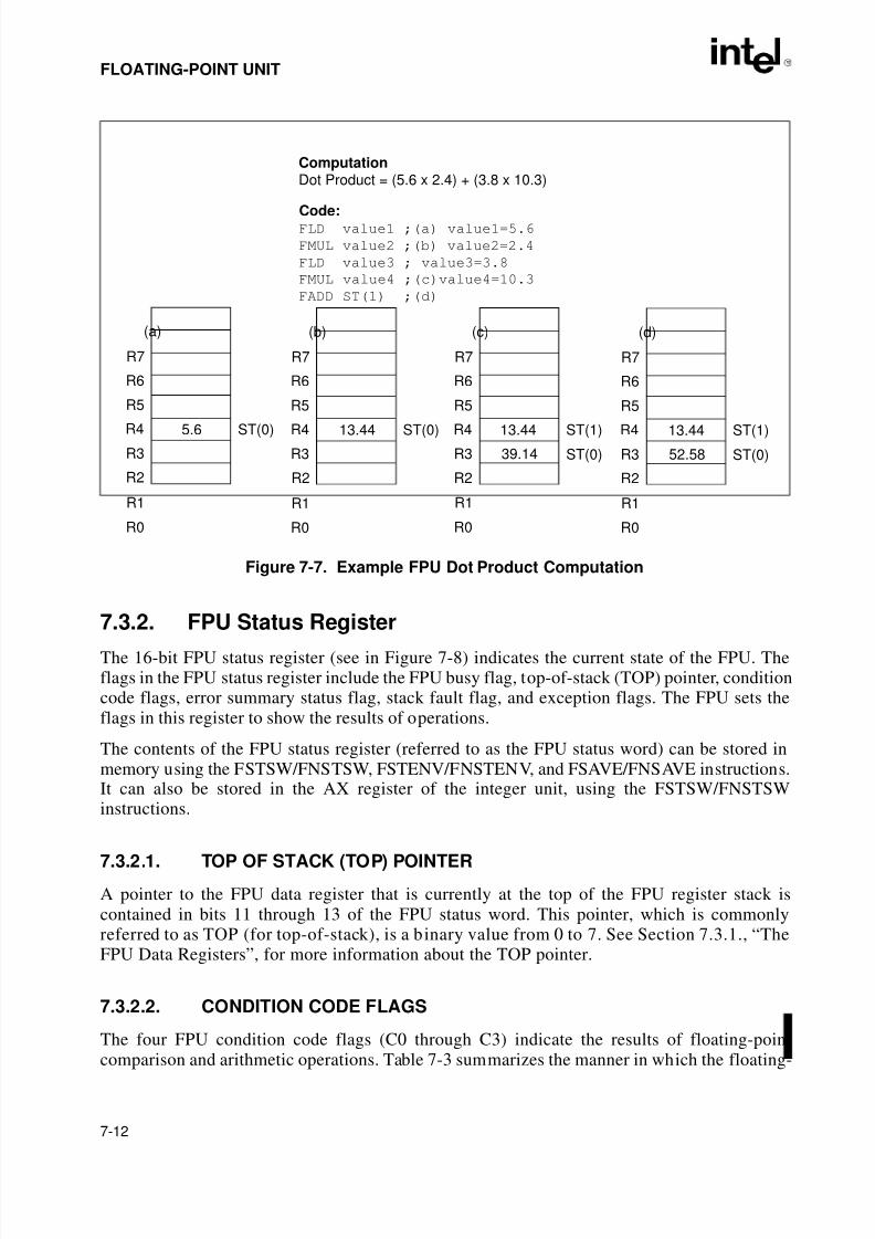
8/3/2019 Intel Architecture Software Developer's Manual, Volume 1: Basic Architecture
http://slidepdf.com/reader/full/intel-architecture-software-developers-manual-volume-1-basic-architecture 148/283
7-12
FLOATING-POINT UNIT
7.3.2. FPU Status Register
The 16-bit FPU status register (see in Figure 7-8) indicates the current state of the FPU. Theflags in the FPU status register include the FPU busy flag, top-of-stack (TOP) pointer, conditioncode flags, error summary status flag, stack fault flag, and exception flags. The FPU sets theflags in this register to show the results of operations.
The contents of the FPU status register (referred to as the FPU status word) can be stored inmemory using the FSTSW/FNSTSW, FSTENV/FNSTENV, and FSAVE/FNSAVE instructions.It can also be stored in the AX register of the integer unit, using the FSTSW/FNSTSWinstructions.
7.3.2.1. TOP OF STACK (TOP) POINTER
A pointer to the FPU data register that is currently at the top of the FPU register stack iscontained in bits 11 through 13 of the FPU status word. This pointer, which is commonlyreferred to as TOP (for top-of-stack), is a binary value from 0 to 7. See Section 7.3.1., “TheFPU Data Registers”, for more information about the TOP pointer.
7.3.2.2. CONDITION CODE FLAGS
The four FPU condition code flags (C0 through C3) indicate the results of floating-point
comparison and arithmetic operations. Table 7-3 summarizes the manner in which the floating-
Figure 7-7. Example FPU Dot Product Computation
(a)
R7
R6
R5
R4
R3
R2
R1
R0
Computation
ST(0)5.6
(b)
R7
R6
R5
R4
R3
R2
R1
R0
ST(0)13.44
(c)
R7
R6
R5
R4
R3
R2
R1
R0
ST(1)
ST(0)
13.44
(d)
R7
R6
R5
R4
R3
R2
R1
R0
ST(1)
ST(0)39.14
13.44
52.58
Dot Product = (5.6 x 2.4) + (3.8 x 10.3)
Code:FLD value1 ;(a) value1=5.6
FMUL value2 ;(b) value2=2.4
FLD value3 ; value3=3.8
FMUL value4 ;(c)value4=10.3
FADD ST(1) ;(d)
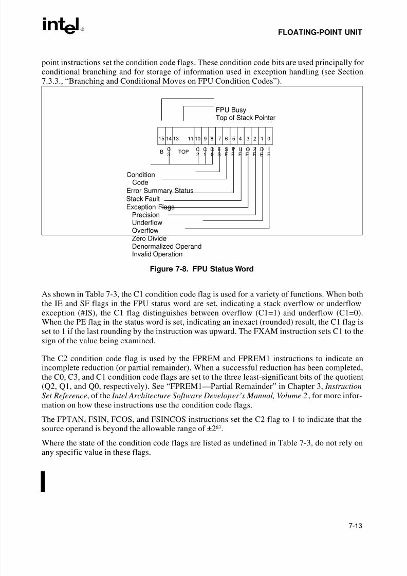
8/3/2019 Intel Architecture Software Developer's Manual, Volume 1: Basic Architecture
http://slidepdf.com/reader/full/intel-architecture-software-developers-manual-volume-1-basic-architecture 149/283
7-13
FLOATING-POINT UNIT
point instructions set the condition code flags. These condition code bits are used principally forconditional branching and for storage of information used in exception handling (see Section7.3.3., “Branching and Conditional Moves on FPU Condition Codes”).
As shown in Table 7-3, the C1 condition code flag is used for a variety of functions. When boththe IE and SF flags in the FPU status word are set, indicating a stack overflow or underflowexception (#IS), the C1 flag distinguishes between overflow (C1=1) and underflow (C1=0).When the PE flag in the status word is set, indicating an inexact (rounded) result, the C1 flag isset to 1 if the last rounding by the instruction was upward. The FXAM instruction sets C1 to thesign of the value being examined.
The C2 condition code flag is used by the FPREM and FPREM1 instructions to indicate anincomplete reduction (or partial remainder). When a successful reduction has been completed,the C0, C3, and C1 condition code flags are set to the three least-significant bits of the quotient(Q2, Q1, and Q0, respectively). See “FPREM1—Partial Remainder” in Chapter 3, Instruction
Set Reference, of the Intel Architecture Software Developer’s Manual, Volume 2 , for more infor-mation on how these instructions use the condition code flags.
The FPTAN, FSIN, FCOS, and FSINCOS instructions set the C2 flag to 1 to indicate that thesource operand is beyond the allowable range of ±263.
Where the state of the condition code flags are listed as undefined in Table 7-3, do not rely onany specific value in these flags.
Figure 7-8. FPU Status Word
FPU Busy
15 1314 11 10 9 8 7 6 5 4 3 2 1 0
BIE
PE
OE
UE
ZE
DE
TOP
Top of Stack Pointer
Exception FlagsPrecisionUnderflowOverflowZero DivideDenormalized OperandInvalid Operation
Stack Fault
Error Summary Status
ConditionCode
C2
C1
C0
ES
SF
C3
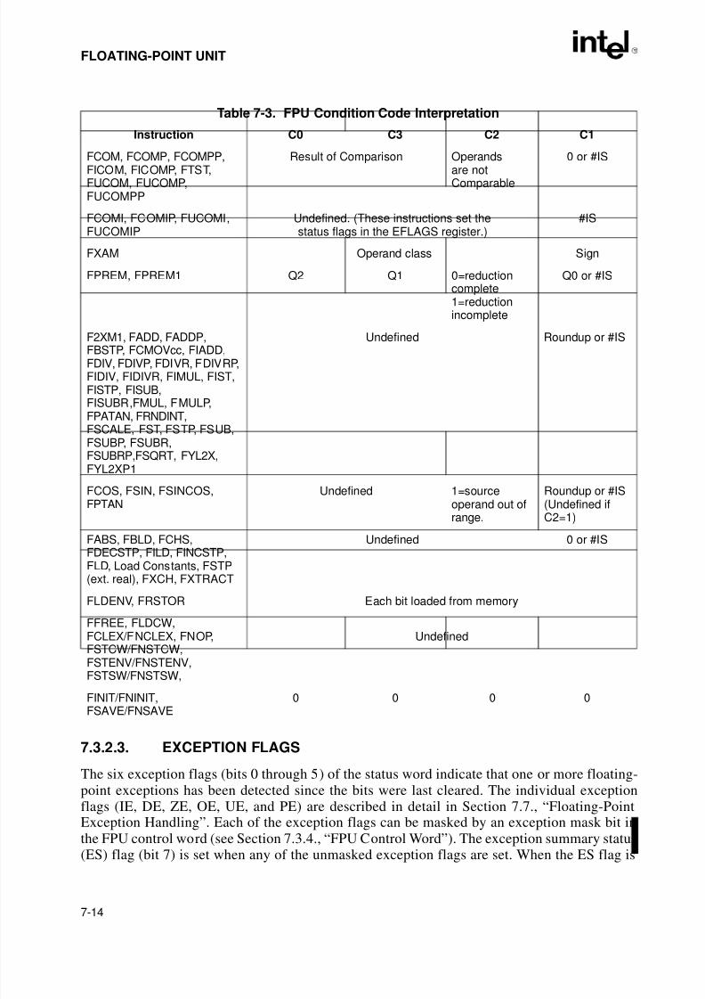
8/3/2019 Intel Architecture Software Developer's Manual, Volume 1: Basic Architecture
http://slidepdf.com/reader/full/intel-architecture-software-developers-manual-volume-1-basic-architecture 150/283
7-14
FLOATING-POINT UNIT
7.3.2.3. EXCEPTION FLAGS
The six exception flags (bits 0 through 5) of the status word indicate that one or more floating-point exceptions has been detected since the bits were last cleared. The individual exceptionflags (IE, DE, ZE, OE, UE, and PE) are described in detail in Section 7.7., “Floating-PointException Handling”. Each of the exception flags can be masked by an exception mask bit inthe FPU control word (see Section 7.3.4., “FPU Control Word”). The exception summary status
(ES) flag (bit 7) is set when any of the unmasked exception flags are set. When the ES flag is
Table 7-3. FPU Condition Code Interpretation
Instruction C0 C3 C2 C1
FCOM, FCOMP, FCOMPP,
FICOM, FICOMP, FTST,FUCOM, FUCOMP,FUCOMPP
Result of Comparison Operands
are notComparable
0 or #IS
FCOMI, FCOMIP, FUCOMI,FUCOMIP
Undefined. (These instructions set thestatus flags in the EFLAGS register.)
#IS
FXAM Operand class Sign
FPREM, FPREM1 Q2 Q1 0=reductioncomplete1=reductionincomplete
Q0 or #IS
F2XM1, FADD, FADDP,FBSTP, FCMOVcc, FIADD,FDIV, FDIVP, FDIVR, FDIVRP,FIDIV, FIDIVR, FIMUL, FIST,FISTP, FISUB,FISUBR,FMUL, FMULP,FPATAN, FRNDINT,FSCALE, FST, FSTP, FSUB,FSUBP, FSUBR,FSUBRP,FSQRT, FYL2X,FYL2XP1
Undefined Roundup or #IS
FCOS, FSIN, FSINCOS,FPTAN
Undefined 1=sourceoperand out of
range.
Roundup or #IS(Undefined if
C2=1)
FABS, FBLD, FCHS,FDECSTP, FILD, FINCSTP,FLD, Load Constants, FSTP(ext. real), FXCH, FXTRACT
Undefined 0 or #IS
FLDENV, FRSTOR Each bit loaded from memory
FFREE, FLDCW,FCLEX/FNCLEX, FNOP,FSTCW/FNSTCW,FSTENV/FNSTENV,FSTSW/FNSTSW,
Undefined
FINIT/FNINIT,FSAVE/FNSAVE
0 0 0 0
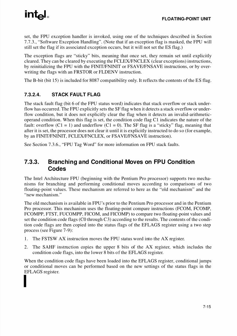
8/3/2019 Intel Architecture Software Developer's Manual, Volume 1: Basic Architecture
http://slidepdf.com/reader/full/intel-architecture-software-developers-manual-volume-1-basic-architecture 151/283
7-15
FLOATING-POINT UNIT
set, the FPU exception handler is invoked, using one of the techniques described in Section7.7.3., “Software Exception Handling”. (Note that if an exception flag is masked, the FPU willstill set the flag if its associated exception occurs, but it will not set the ES flag.)
The exception flags are “sticky” bits, meaning that once set, they remain set until explicitlycleared. They can be cleared by executing the FCLEX/FNCLEX (clear exceptions) instructions,by reinitializing the FPU with the FINIT/FNINIT or FSAVE/FNSAVE instructions, or by over-writing the flags with an FRSTOR or FLDENV instruction.
The B-bit (bit 15) is included for 8087 compatibility only. It reflects the contents of the ES flag.
7.3.2.4. STACK FAULT FLAG
The stack fault flag (bit 6 of the FPU status word) indicates that stack overflow or stack under-flow has occurred. The FPU explicitly sets the SF flag when it detects a stack overflow or under-
flow condition, but it does not explicitly clear the flag when it detects an invalid-arithmetic-operand condition. When this flag is set, the condition code flag C1 indicates the nature of thefault: overflow (C1 = 1) and underflow (C1 = 0). The SF flag is a “sticky” flag, meaning thatafter it is set, the processor does not clear it until it is explicitly instructed to do so (for example,by an FINIT/FNINIT, FCLEX/FNCLEX, or FSAVE/FNSAVE instruction).
See Section 7.3.6., “FPU Tag Word” for more information on FPU stack faults.
7.3.3. Branching and Conditional Moves on FPU ConditionCodes
The Intel Architecture FPU (beginning with the Pentium Pro processor) supports two mecha-nisms for branching and performing conditional moves according to comparisons of twofloating-point values. These mechanism are referred to here as the “old mechanism” and the“new mechanism.”
The old mechanism is available in FPU’s prior to the Pentium Pro processor and in the PentiumPro processor. This mechanism uses the floating-point compare instructions (FCOM, FCOMP,FCOMPP, FTST, FUCOMPP, FICOM, and FICOMP) to compare two floating-point values andset the condition code flags (C0 through C3) according to the results. The contents of the condi-tion code flags are then copied into the status flags of the EFLAGS register using a two step
process (see Figure 7-9):
1. The FSTSW AX instruction moves the FPU status word into the AX register.
2. The SAHF instruction copies the upper 8 bits of the AX register, which includes thecondition code flags, into the lower 8 bits of the EFLAGS register.
When the condition code flags have been loaded into the EFLAGS register, conditional jumpsor conditional moves can be performed based on the new settings of the status flags in theEFLAGS register.
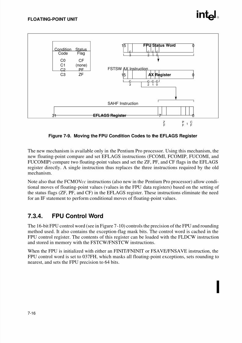
8/3/2019 Intel Architecture Software Developer's Manual, Volume 1: Basic Architecture
http://slidepdf.com/reader/full/intel-architecture-software-developers-manual-volume-1-basic-architecture 152/283
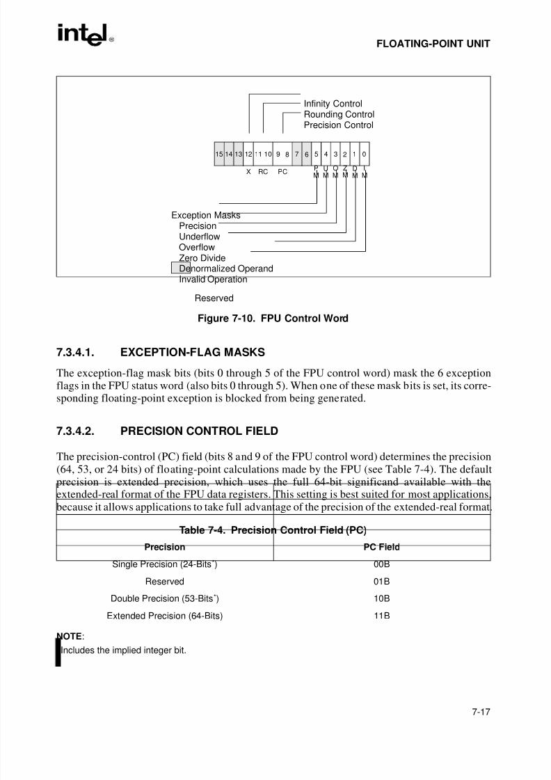
8/3/2019 Intel Architecture Software Developer's Manual, Volume 1: Basic Architecture
http://slidepdf.com/reader/full/intel-architecture-software-developers-manual-volume-1-basic-architecture 153/283
7-17
FLOATING-POINT UNIT
7.3.4.1. EXCEPTION-FLAG MASKS
The exception-flag mask bits (bits 0 through 5 of the FPU control word) mask the 6 exceptionflags in the FPU status word (also bits 0 through 5). When one of these mask bits is set, its corre-
sponding floating-point exception is blocked from being generated.
7.3.4.2. PRECISION CONTROL FIELD
The precision-control (PC) field (bits 8 and 9 of the FPU control word) determines the precision(64, 53, or 24 bits) of floating-point calculations made by the FPU (see Table 7-4). The defaultprecision is extended precision, which uses the full 64-bit significand available with theextended-real format of the FPU data registers. This setting is best suited for most applications,because it allows applications to take full advantage of the precision of the extended-real format.
NOTE:
* Includes the implied integer bit.
Figure 7-10. FPU Control Word
Table 7-4. Precision Control Field (PC)Precision PC Field
Single Precision (24-Bits*) 00B
Reserved 01B
Double Precision (53-Bits*) 10B
Extended Precision (64-Bits) 11B
15 1314 12 11 10 9 8 7 6 5 4 3 2 1 0
XIM
PM
OM
UM
ZM
DM
RC PC
Infinity ControlRounding ControlPrecision Control
Exception MasksPrecisionUnderflowOverflowZero Divide
Denormalized OperandInvalid Operation
Reserved
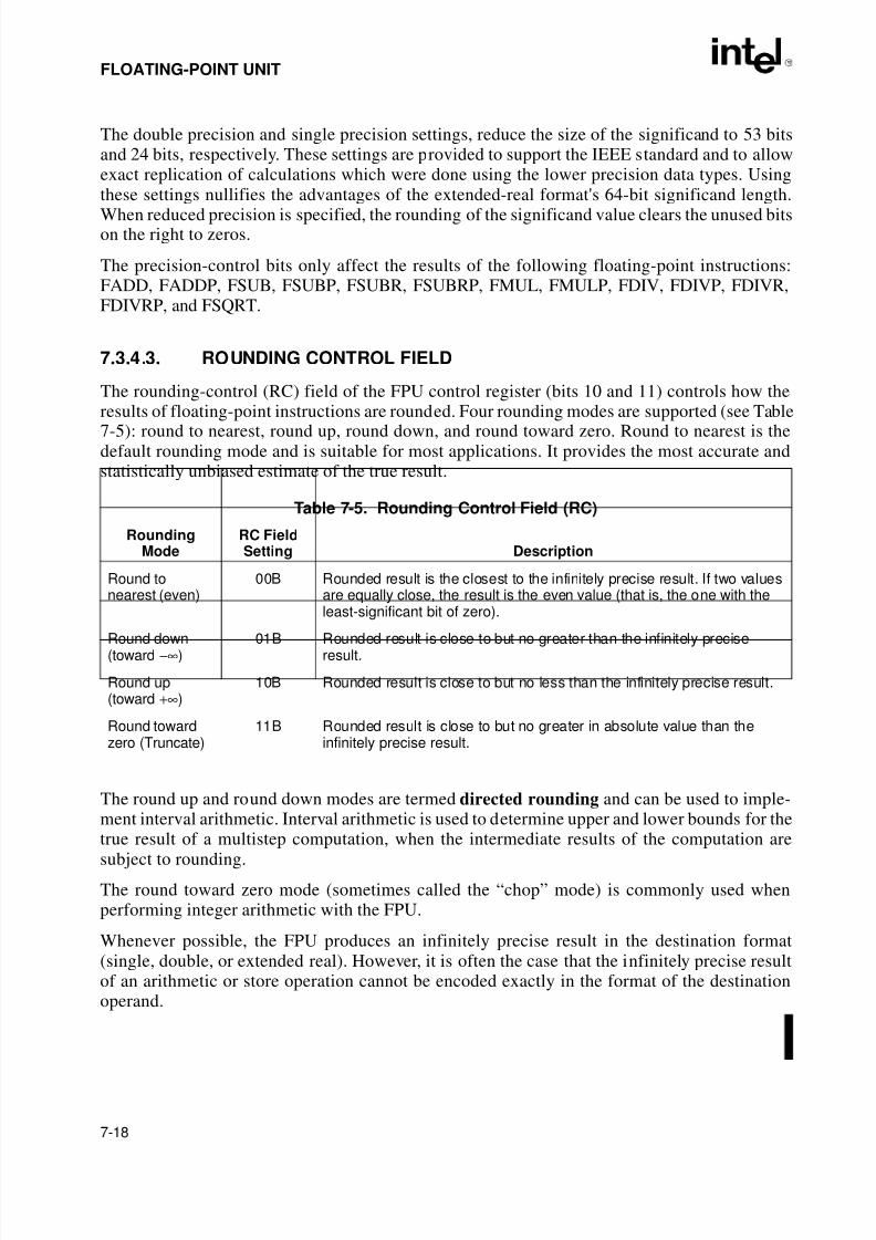
8/3/2019 Intel Architecture Software Developer's Manual, Volume 1: Basic Architecture
http://slidepdf.com/reader/full/intel-architecture-software-developers-manual-volume-1-basic-architecture 154/283
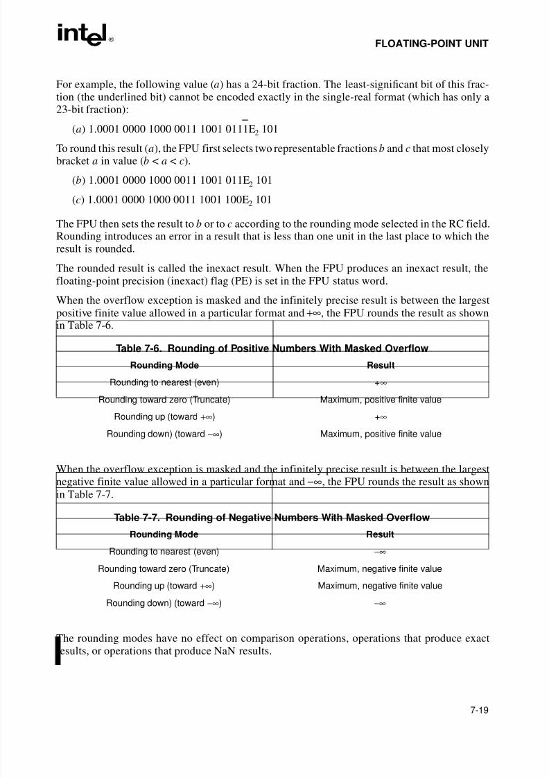
8/3/2019 Intel Architecture Software Developer's Manual, Volume 1: Basic Architecture
http://slidepdf.com/reader/full/intel-architecture-software-developers-manual-volume-1-basic-architecture 155/283
7-19
FLOATING-POINT UNIT
For example, the following value (a) has a 24-bit fraction. The least-significant bit of this frac-tion (the underlined bit) cannot be encoded exactly in the single-real format (which has only a23-bit fraction):
(a) 1.0001 0000 1000 0011 1001 0111E2 101To round this result (a), the FPU first selects two representable fractions b and c that most closelybracket a in value (b < a < c).
(b) 1.0001 0000 1000 0011 1001 011E2 101
(c) 1.0001 0000 1000 0011 1001 100E2 101
The FPU then sets the result to b or to c according to the rounding mode selected in the RC field.Rounding introduces an error in a result that is less than one unit in the last place to which theresult is rounded.
The rounded result is called the inexact result. When the FPU produces an inexact result, thefloating-point precision (inexact) flag (PE) is set in the FPU status word.
When the overflow exception is masked and the infinitely precise result is between the largestpositive finite value allowed in a particular format and +∞, the FPU rounds the result as shownin Table 7-6.
When the overflow exception is masked and the infinitely precise result is between the largestnegative finite value allowed in a particular format and −∞, the FPU rounds the result as shownin Table 7-7.
The rounding modes have no effect on comparison operations, operations that produce exactresults, or operations that produce NaN results.
Table 7-6. Rounding of Positive Numbers With Masked Overflow
Rounding Mode Result
Rounding to nearest (even) +∞
Rounding toward zero (Truncate) Maximum, positive finite value
Rounding up (toward +∞) +∞
Rounding down) (toward −∞) Maximum, positive finite value
Table 7-7. Rounding of Negative Numbers With Masked Overflow
Rounding Mode Result
Rounding to nearest (even) −∞
Rounding toward zero (Truncate) Maximum, negative finite value
Rounding up (toward +∞) Maximum, negative finite value
Rounding down) (toward −∞) −∞
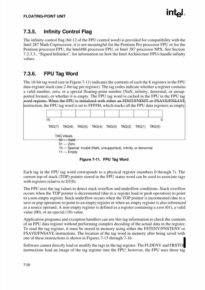
8/3/2019 Intel Architecture Software Developer's Manual, Volume 1: Basic Architecture
http://slidepdf.com/reader/full/intel-architecture-software-developers-manual-volume-1-basic-architecture 156/283
7-20
FLOATING-POINT UNIT
7.3.5. Infinity Control Flag
The infinity control flag (bit 12 of the FPU control word) is provided for compatibility with theIntel 287 Math Coprocessor; it is not meaningful for the Pentium Pro processor FPU or for the
Pentium processor FPU, the Intel486 processor FPU, or Intel 387 processor NPX. See Section7.2.3.3., “Signed Infinities”, for information on how the Intel Architecture FPUs handle infinityvalues.
7.3.6. FPU Tag Word
The 16-bit tag word (see in Figure 7-11) indicates the contents of each the 8 registers in the FPUdata-register stack (one 2-bit tag per register). The tag codes indicate whether a register containsa valid number, zero, or a special floating-point number (NaN, infinity, denormal, or unsup-ported format), or whether it is empty. The FPU tag word is cached in the FPU in the FPU tag
word register. When the FPU is initialized with either an FINIT/FNINIT or FSAVE/FNSAVEinstruction, the FPU tag word is set to FFFFH, which marks all the FPU data registers as empty.
.
Each tag in the FPU tag word corresponds to a physical register (numbers 0 through 7). Thecurrent top-of-stack (TOP) pointer stored in the FPU status word can be used to associate tagswith registers relative to ST(0).
The FPU uses the tag values to detect stack overflow and underflow conditions. Stack overflowoccurs when the TOP pointer is decremented (due to a register load or push operation) to point
to a non-empty register. Stack underflow occurs when the TOP pointer is incremented (due to asave or pop operation) to point to an empty register or when an empty register is also referencedas a source operand. A non-empty register is defined as a register containing a zero (01), a validvalue (00), or an special (10) value.
Application programs and exception handlers can use this tag information to check the contentsof an FPU data register without performing complex decoding of the actual data in the register.To read the tag register, it must be stored in memory using either the FSTENV/FNSTENV orFSAVE/FNSAVE instructions. The location of the tag word in memory after being saved withone of these instructions is shown in Figures 7-13 through 7-16.
Software cannot directly load or modify the tags in the tag register. The FLDENV and FRSTOR
instructions load an image of the tag register into the FPU; however, the FPU uses those tag
Figure 7-11. FPU Tag Word
015
TAG Values
TAG(7) TAG(5)TAG(6) TAG(4) TAG(3) TAG(2) TAG(1) TAG(0)
00 — Valid01 — Zero
10 — Special: invalid (NaN, unsupported), infinity, or denormal11 — Empty
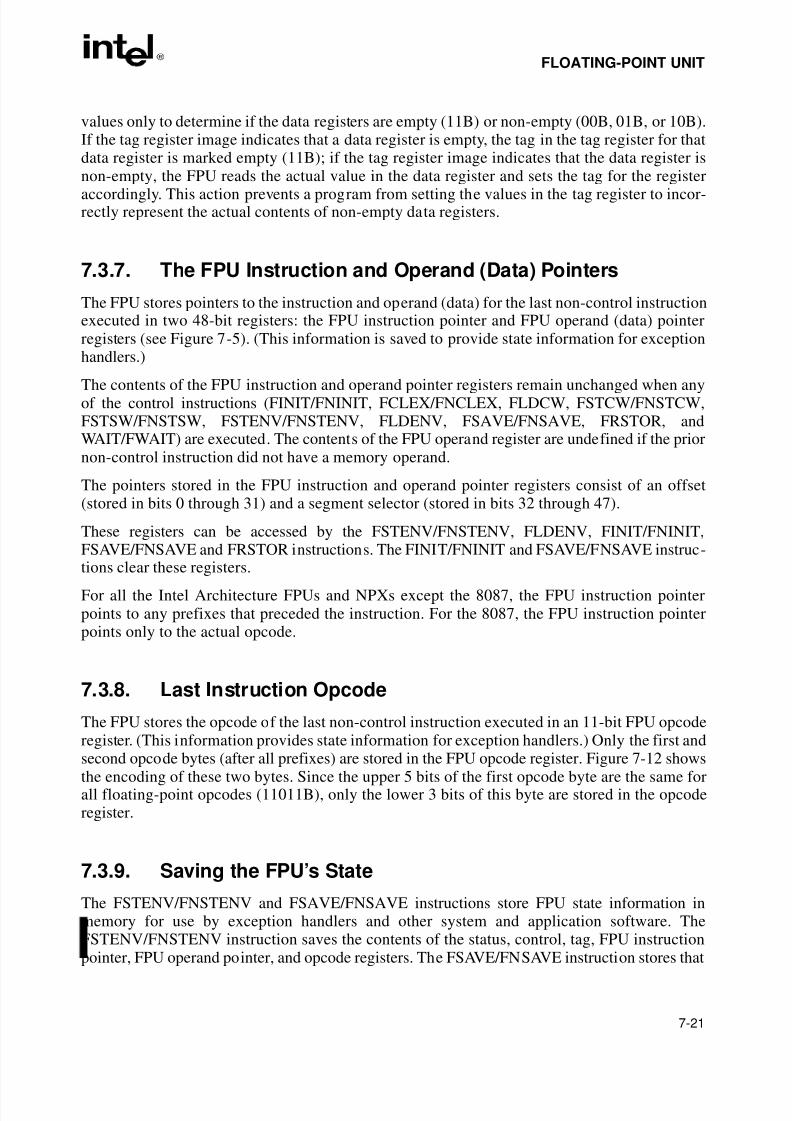
8/3/2019 Intel Architecture Software Developer's Manual, Volume 1: Basic Architecture
http://slidepdf.com/reader/full/intel-architecture-software-developers-manual-volume-1-basic-architecture 157/283
7-21
FLOATING-POINT UNIT
values only to determine if the data registers are empty (11B) or non-empty (00B, 01B, or 10B).If the tag register image indicates that a data register is empty, the tag in the tag register for thatdata register is marked empty (11B); if the tag register image indicates that the data register isnon-empty, the FPU reads the actual value in the data register and sets the tag for the register
accordingly. This action prevents a program from setting the values in the tag register to incor-rectly represent the actual contents of non-empty data registers.
7.3.7. The FPU Instruction and Operand (Data) Pointers
The FPU stores pointers to the instruction and operand (data) for the last non-control instructionexecuted in two 48-bit registers: the FPU instruction pointer and FPU operand (data) pointerregisters (see Figure 7-5). (This information is saved to provide state information for exceptionhandlers.)
The contents of the FPU instruction and operand pointer registers remain unchanged when anyof the control instructions (FINIT/FNINIT, FCLEX/FNCLEX, FLDCW, FSTCW/FNSTCW,FSTSW/FNSTSW, FSTENV/FNSTENV, FLDENV, FSAVE/FNSAVE, FRSTOR, andWAIT/FWAIT) are executed. The contents of the FPU operand register are undefined if the priornon-control instruction did not have a memory operand.
The pointers stored in the FPU instruction and operand pointer registers consist of an offset(stored in bits 0 through 31) and a segment selector (stored in bits 32 through 47).
These registers can be accessed by the FSTENV/FNSTENV, FLDENV, FINIT/FNINIT,FSAVE/FNSAVE and FRSTOR instructions. The FINIT/FNINIT and FSAVE/FNSAVE instruc-tions clear these registers.
For all the Intel Architecture FPUs and NPXs except the 8087, the FPU instruction pointerpoints to any prefixes that preceded the instruction. For the 8087, the FPU instruction pointerpoints only to the actual opcode.
7.3.8. Last Instruction Opcode
The FPU stores the opcode of the last non-control instruction executed in an 11-bit FPU opcoderegister. (This information provides state information for exception handlers.) Only the first andsecond opcode bytes (after all prefixes) are stored in the FPU opcode register. Figure 7-12 showsthe encoding of these two bytes. Since the upper 5 bits of the first opcode byte are the same forall floating-point opcodes (11011B), only the lower 3 bits of this byte are stored in the opcoderegister.
7.3.9. Saving the FPU’s State
The FSTENV/FNSTENV and FSAVE/FNSAVE instructions store FPU state information inmemory for use by exception handlers and other system and application software. TheFSTENV/FNSTENV instruction saves the contents of the status, control, tag, FPU instruction
pointer, FPU operand pointer, and opcode registers. The FSAVE/FNSAVE instruction stores that

8/3/2019 Intel Architecture Software Developer's Manual, Volume 1: Basic Architecture
http://slidepdf.com/reader/full/intel-architecture-software-developers-manual-volume-1-basic-architecture 158/283
7-22
FLOATING-POINT UNIT
information plus the contents of the FPU data registers. Note that the FSAVE/FNSAVE instruc-tion also initializes the FPU to default values (just as the FINIT/FNINIT instruction does) afterit has saved the original state of the FPU.
The manner in which this information is stored in memory depends on the operating mode of the processor (protected mode or real-address mode) and on the operand-size attribute in effect(32-bit or 16-bit). See Figures 7-13 through 7-16. In virtual-8086 mode or SMM, the real-address mode formats shown in Figure 7-16 is used. See “Using the FPU in SMM” in Chapter11 of the Intel Architecture Software Developer’s Manual, Volume 3, for special considerationsfor using the FPU while in SMM.
Figure 7-12. Contents of FPU Opcode Registers
Figure 7-13. Protected Mode FPU State Image in Memory, 32-Bit Format
0
FPU Opcode Register
10
02nd Instruction Byte
701st Instruction Byte
7 2
78
031
0
4
8
12
16
20
24
32-Bit Protected Mode Format
Control Word
15
Opcode 10...00
Status Word
Tag Word
FPU Instruction Pointer Selector
FPU Operand Pointer Selector
FPU Operand Pointer Offset
0 0 0 0
FPU Instruction Pointer Offset
Reserved
16
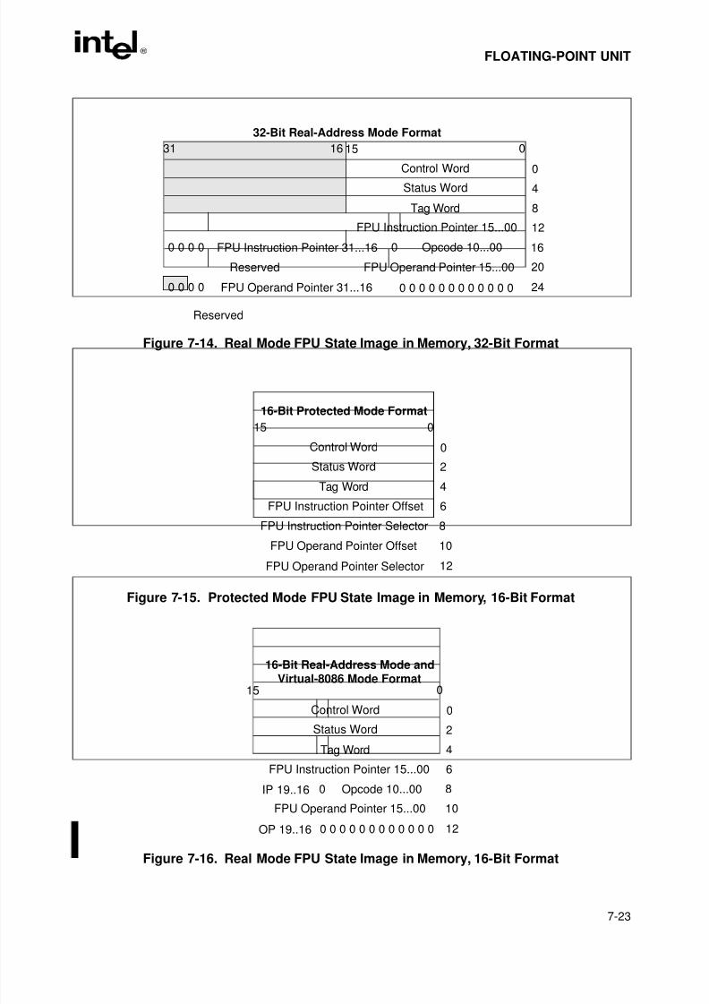
8/3/2019 Intel Architecture Software Developer's Manual, Volume 1: Basic Architecture
http://slidepdf.com/reader/full/intel-architecture-software-developers-manual-volume-1-basic-architecture 159/283
7-23
FLOATING-POINT UNIT
Figure 7-14. Real Mode FPU State Image in Memory, 32-Bit Format
Figure 7-15. Protected Mode FPU State Image in Memory, 16-Bit Format
Figure 7-16. Real Mode FPU State Image in Memory, 16-Bit Format
031
04
8
12
16
20
24
32-Bit Real-Address Mode Format
Control Word
15
FPU Operand Pointer 31...16
FPU Instruction Pointer 31...16
Status Word
Tag Word
Opcode 10...00
0 0 0 0 0 0 0 0 0 0 0 0
FPU Operand Pointer 15...00
0 0 0 0
FPU Instruction Pointer 15...00
0 0 0 0
Reserved
0
Reserved
16
0
0
2
4
6
8
10
12
16-Bit Protected Mode Format
Control Word
15
Status Word
Tag Word
FPU Instruction Pointer Selector
FPU Operand Pointer Selector
FPU Operand Pointer Offset
FPU Instruction Pointer Offset
0
0
2
4
6
8
10
12
16-Bit Real-Address Mode and
Control Word
15
Status Word
Tag Word
Virtual-8086 Mode Format
0 0 0 0 0 0 0 0 0 0 0 0
Opcode 10...000
FPU Instruction Pointer 15...00
IP 19..16
OP 19..16
FPU Operand Pointer 15...00
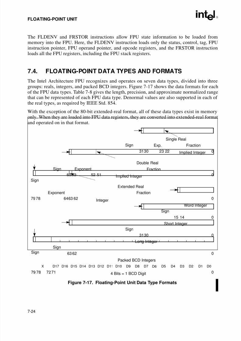
8/3/2019 Intel Architecture Software Developer's Manual, Volume 1: Basic Architecture
http://slidepdf.com/reader/full/intel-architecture-software-developers-manual-volume-1-basic-architecture 160/283
7-24
FLOATING-POINT UNIT
The FLDENV and FRSTOR instructions allow FPU state information to be loaded frommemory into the FPU. Here, the FLDENV instruction loads only the status, control, tag, FPUinstruction pointer, FPU operand pointer, and opcode registers, and the FRSTOR instructionloads all the FPU registers, including the FPU stack registers.
7.4. FLOATING-POINT DATA TYPES AND FORMATS
The Intel Architecture FPU recognizes and operates on seven data types, divided into threegroups: reals, integers, and packed BCD integers. Figure 7-17 shows the data formats for eachof the FPU data types. Table 7-8 gives the length, precision, and approximate normalized rangethat can be represented of each FPU data type. Denormal values are also supported in each of the real types, as required by IEEE Std. 854.
With the exception of the 80-bit extended-real format, all of these data types exist in memory
only. When they are loaded into FPU data registers, they are converted into extended-real formatand operated on in that format.
Figure 7-17. Floating-Point Unit Data Type Formats
0
Packed BCD Integers
79
D0
0
Long Integer
63
4 Bits = 1 BCD Digit
0
Short Integer
31
0
Word Integer
15
Sign
D1D2D3D4D5D6D7D8D9D10D11D12D13D14D15D16D17
78 7271
X
62
14
30
0
Extended Real
79
Sign
78 6463
0
Double Real
6362
0
Single Real
3130 23 22
FractionExp.Sign
Implied Integer
Implied Integer
Sign Exponent Fraction
52 51
FractionExponent
62 Integer
Sign
Sign
Sign
8/3/2019 Intel Architecture Software Developer's Manual, Volume 1: Basic Architecture
http://slidepdf.com/reader/full/intel-architecture-software-developers-manual-volume-1-basic-architecture 161/283
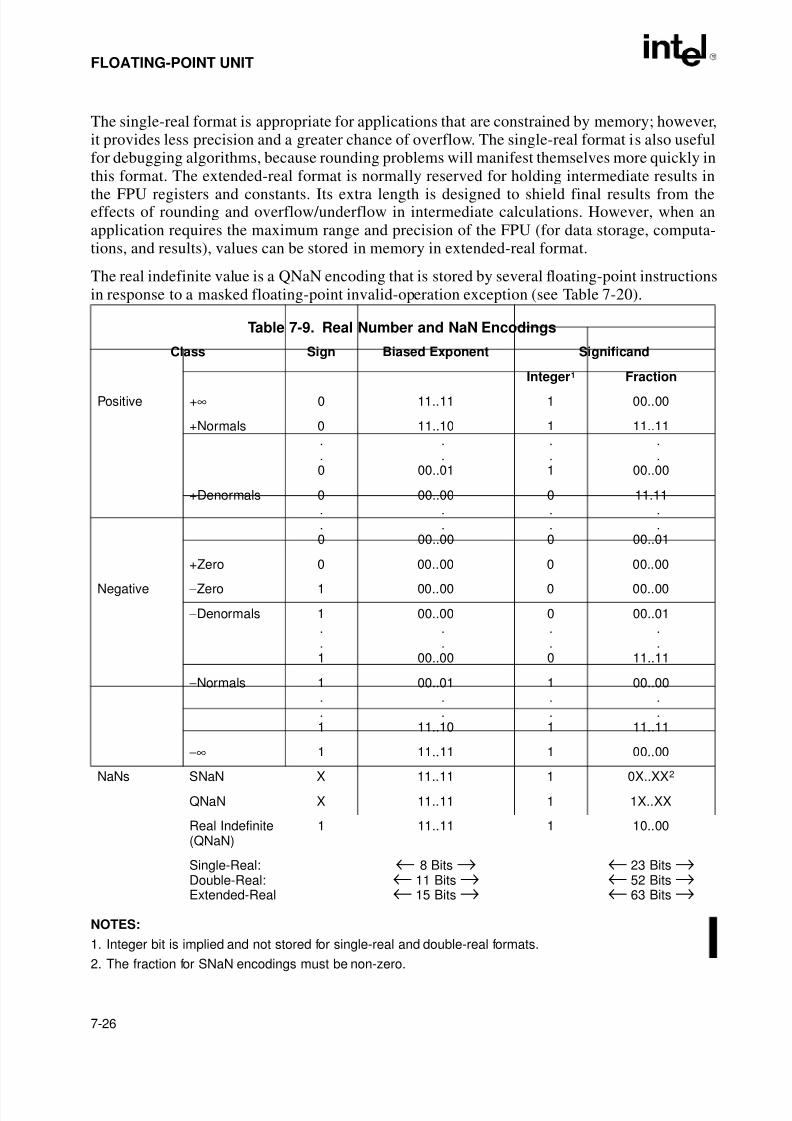
8/3/2019 Intel Architecture Software Developer's Manual, Volume 1: Basic Architecture
http://slidepdf.com/reader/full/intel-architecture-software-developers-manual-volume-1-basic-architecture 162/283
7-26
FLOATING-POINT UNIT
The single-real format is appropriate for applications that are constrained by memory; however,it provides less precision and a greater chance of overflow. The single-real format is also usefulfor debugging algorithms, because rounding problems will manifest themselves more quickly inthis format. The extended-real format is normally reserved for holding intermediate results in
the FPU registers and constants. Its extra length is designed to shield final results from theeffects of rounding and overflow/underflow in intermediate calculations. However, when anapplication requires the maximum range and precision of the FPU (for data storage, computa-tions, and results), values can be stored in memory in extended-real format.
The real indefinite value is a QNaN encoding that is stored by several floating-point instructionsin response to a masked floating-point invalid-operation exception (see Table 7-20).
NOTES:
1. Integer bit is implied and not stored for single-real and double-real formats.
2. The fraction for SNaN encodings must be non-zero.
Table 7-9. Real Number and NaN Encodings
Class Sign Biased Exponent Significand
Integer1 Fraction
Positive +∞ 0 11..11 1 00..00
+Normals 0..0
11..10..
00..01
1..1
11..11..
00..00
+Denormals 0..0
00..00..
00..00
0..0
11.11..
00..01
+Zero 0 00..00 0 00..00
Negative −Zero 1 00..00 0 00..00
−Denormals 1..1
00..00..
00..00
0..0
00..01..
11..11
−Normals 1..1
00..01..
11..10
1..1
00..00..
11..11
−∞ 1 11..11 1 00..00
NaNs SNaN X 11..11 1 0X..XX2
QNaN X 11..11 1 1X..XX
Real Indefinite(QNaN)
1 11..11 1 10..00
Single-Real:Double-Real:Extended-Real
← 8 Bits →← 11 Bits →← 15 Bits →
← 23 Bits →← 52 Bits →← 63 Bits →
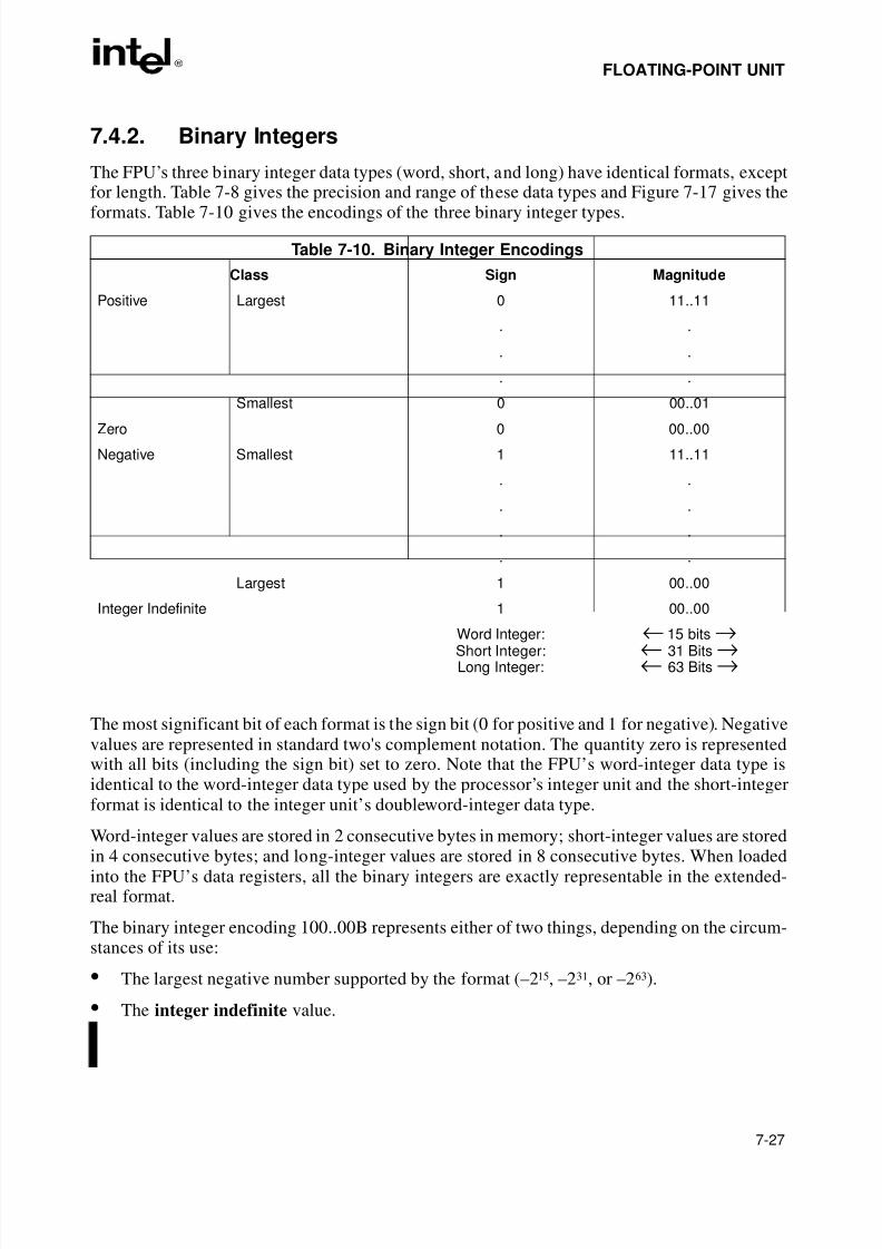
8/3/2019 Intel Architecture Software Developer's Manual, Volume 1: Basic Architecture
http://slidepdf.com/reader/full/intel-architecture-software-developers-manual-volume-1-basic-architecture 163/283
7-27
FLOATING-POINT UNIT
7.4.2. Binary Integers
The FPU’s three binary integer data types (word, short, and long) have identical formats, exceptfor length. Table 7-8 gives the precision and range of these data types and Figure 7-17 gives the
formats. Table 7-10 gives the encodings of the three binary integer types.
The most significant bit of each format is the sign bit (0 for positive and 1 for negative). Negativevalues are represented in standard two's complement notation. The quantity zero is representedwith all bits (including the sign bit) set to zero. Note that the FPU’s word-integer data type isidentical to the word-integer data type used by the processor’s integer unit and the short-integerformat is identical to the integer unit’s doubleword-integer data type.
Word-integer values are stored in 2 consecutive bytes in memory; short-integer values are stored
in 4 consecutive bytes; and long-integer values are stored in 8 consecutive bytes. When loadedinto the FPU’s data registers, all the binary integers are exactly representable in the extended-real format.
The binary integer encoding 100..00B represents either of two things, depending on the circum-stances of its use:
• The largest negative number supported by the format (–215, –231, or –263).
• The integer indefinite value.
Table 7-10. Binary Integer Encodings
Class Sign Magnitude
Positive Largest 0 11..11
. .
. .
. .
Smallest 0 00..01
Zero 0 00..00
Negative Smallest 1 11..11
. .
. .
. .
. .
Largest 1 00..00
Integer Indefinite 1 00..00
Word Integer:Short Integer:Long Integer:
← 15 bits
→← 31 Bits →← 63 Bits →
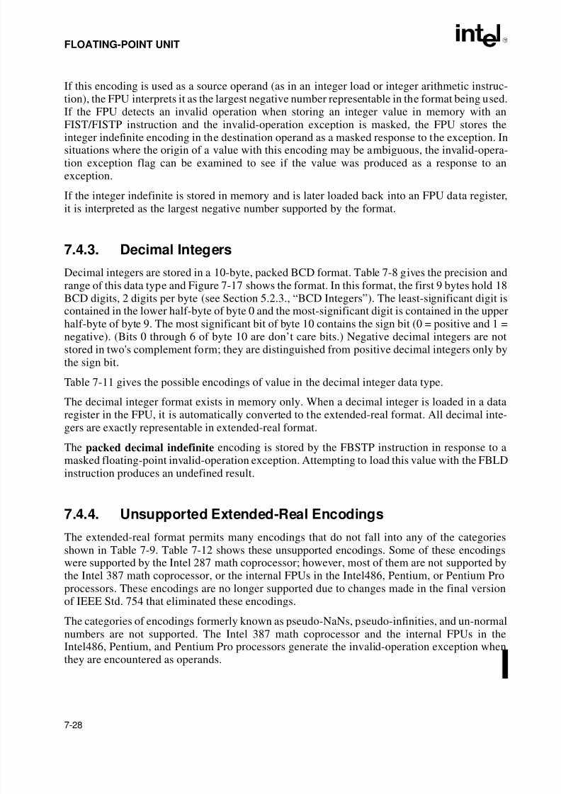
8/3/2019 Intel Architecture Software Developer's Manual, Volume 1: Basic Architecture
http://slidepdf.com/reader/full/intel-architecture-software-developers-manual-volume-1-basic-architecture 164/283
7-28
FLOATING-POINT UNIT
If this encoding is used as a source operand (as in an integer load or integer arithmetic instruc-tion), the FPU interprets it as the largest negative number representable in the format being used.If the FPU detects an invalid operation when storing an integer value in memory with anFIST/FISTP instruction and the invalid-operation exception is masked, the FPU stores the
integer indefinite encoding in the destination operand as a masked response to the exception. Insituations where the origin of a value with this encoding may be ambiguous, the invalid-opera-tion exception flag can be examined to see if the value was produced as a response to anexception.
If the integer indefinite is stored in memory and is later loaded back into an FPU data register,it is interpreted as the largest negative number supported by the format.
7.4.3. Decimal Integers
Decimal integers are stored in a 10-byte, packed BCD format. Table 7-8 gives the precision andrange of this data type and Figure 7-17 shows the format. In this format, the first 9 bytes hold 18BCD digits, 2 digits per byte (see Section 5.2.3., “BCD Integers”). The least-significant digit iscontained in the lower half-byte of byte 0 and the most-significant digit is contained in the upperhalf-byte of byte 9. The most significant bit of byte 10 contains the sign bit (0 = positive and 1 =negative). (Bits 0 through 6 of byte 10 are don’t care bits.) Negative decimal integers are notstored in two's complement form; they are distinguished from positive decimal integers only bythe sign bit.
Table 7-11 gives the possible encodings of value in the decimal integer data type.
The decimal integer format exists in memory only. When a decimal integer is loaded in a dataregister in the FPU, it is automatically converted to the extended-real format. All decimal inte-gers are exactly representable in extended-real format.
The packed decimal indefinite encoding is stored by the FBSTP instruction in response to amasked floating-point invalid-operation exception. Attempting to load this value with the FBLDinstruction produces an undefined result.
7.4.4. Unsupported Extended-Real Encodings
The extended-real format permits many encodings that do not fall into any of the categoriesshown in Table 7-9. Table 7-12 shows these unsupported encodings. Some of these encodingswere supported by the Intel 287 math coprocessor; however, most of them are not supported bythe Intel 387 math coprocessor, or the internal FPUs in the Intel486, Pentium, or Pentium Proprocessors. These encodings are no longer supported due to changes made in the final versionof IEEE Std. 754 that eliminated these encodings.
The categories of encodings formerly known as pseudo-NaNs, pseudo-infinities, and un-normalnumbers are not supported. The Intel 387 math coprocessor and the internal FPUs in theIntel486, Pentium, and Pentium Pro processors generate the invalid-operation exception whenthey are encountered as operands.
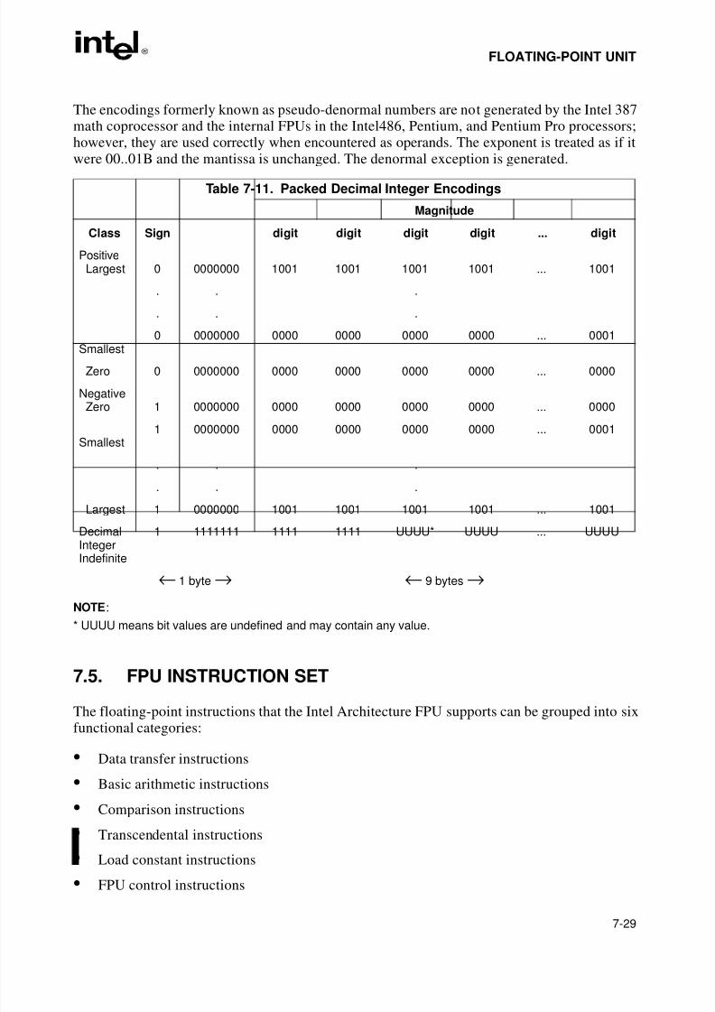
8/3/2019 Intel Architecture Software Developer's Manual, Volume 1: Basic Architecture
http://slidepdf.com/reader/full/intel-architecture-software-developers-manual-volume-1-basic-architecture 165/283
7-29
FLOATING-POINT UNIT
The encodings formerly known as pseudo-denormal numbers are not generated by the Intel 387math coprocessor and the internal FPUs in the Intel486, Pentium, and Pentium Pro processors;however, they are used correctly when encountered as operands. The exponent is treated as if itwere 00..01B and the mantissa is unchanged. The denormal exception is generated.
NOTE:
* UUUU means bit values are undefined and may contain any value.
7.5. FPU INSTRUCTION SET
The floating-point instructions that the Intel Architecture FPU supports can be grouped into sixfunctional categories:
• Data transfer instructions
• Basic arithmetic instructions
• Comparison instructions
• Transcendental instructions
•Load constant instructions
• FPU control instructions
Table 7-11. Packed Decimal Integer Encodings
Magnitude
Class Sign digit digit digit digit ... digit
PositiveLargest 0 0000000 1001 1001 1001 1001 ... 1001
. . .
. . .
Smallest
0 0000000 0000 0000 0000 0000 ... 0001
Zero 0 0000000 0000 0000 0000 0000 ... 0000
NegativeZero 1 0000000 0000 0000 0000 0000 ... 0000
Smallest
1 0000000 0000 0000 0000 0000 ... 0001
. . .
. . .
Largest 1 0000000 1001 1001 1001 1001 ... 1001
DecimalIntegerIndefinite
1 1111111 1111 1111 UUUU* UUUU ... UUUU
← 1 byte → ← 9 bytes →
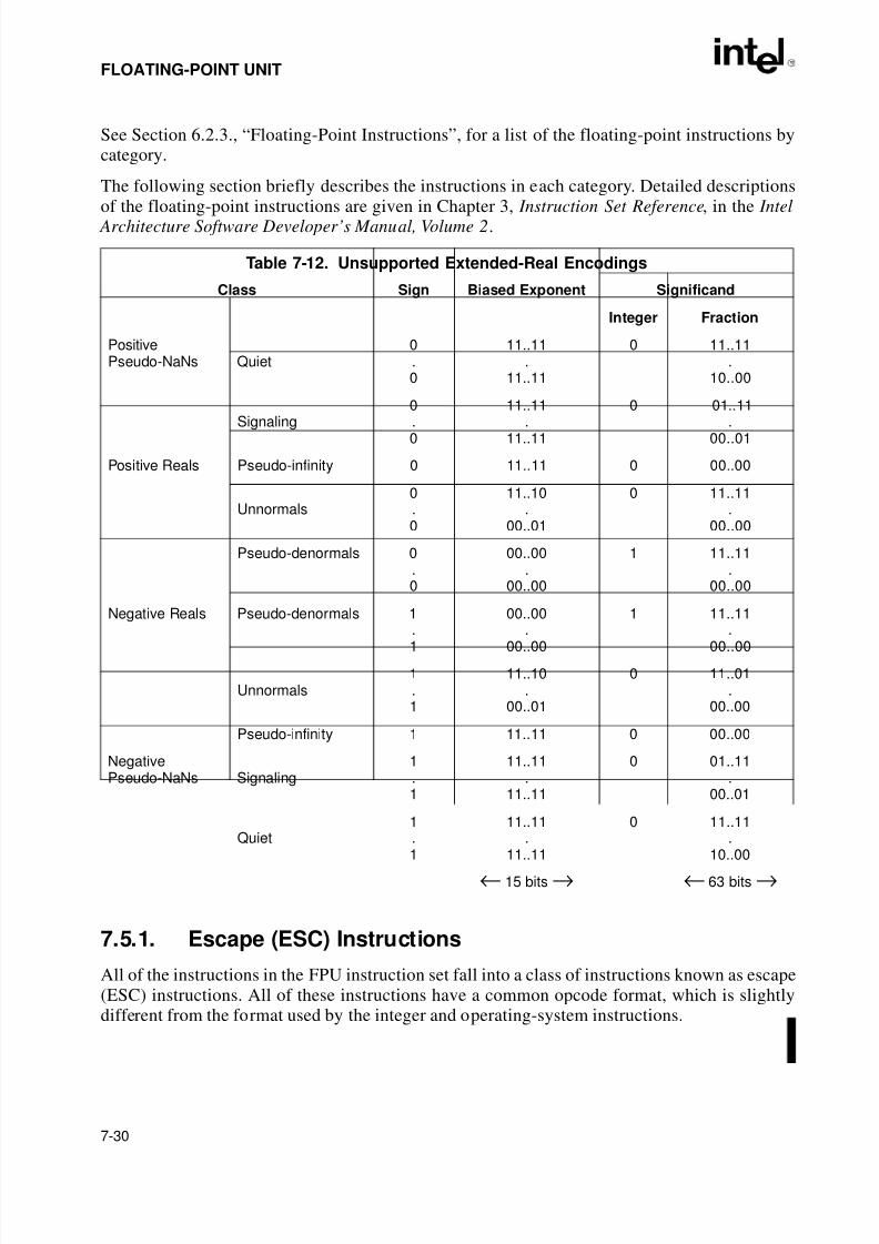
8/3/2019 Intel Architecture Software Developer's Manual, Volume 1: Basic Architecture
http://slidepdf.com/reader/full/intel-architecture-software-developers-manual-volume-1-basic-architecture 166/283
7-30
FLOATING-POINT UNIT
See Section 6.2.3., “Floating-Point Instructions”, for a list of the floating-point instructions bycategory.
The following section briefly describes the instructions in each category. Detailed descriptions
of the floating-point instructions are given in Chapter 3, Instruction Set Reference, in the Intel Architecture Software Developer’s Manual, Volume 2.
7.5.1. Escape (ESC) Instructions
All of the instructions in the FPU instruction set fall into a class of instructions known as escape(ESC) instructions. All of these instructions have a common opcode format, which is slightlydifferent from the format used by the integer and operating-system instructions.
Table 7-12. Unsupported Extended-Real Encodings
Class Sign Biased Exponent Significand
Integer Fraction
PositivePseudo-NaNs Quiet
0.0
11..11.
11..11
0 11..11.
10..00
Signaling
0
.0
11..11
.11..11
0 01..11
.00..01
Positive Reals Pseudo-infinity 0 11..11 0 00..00
Unnormals0.0
11..10.
00..01
0 11..11.
00..00
Pseudo-denormals 0.0
00..00.
00..00
1 11..11.
00..00
Negative Reals Pseudo-denormals 1.1
00..00.
00..00
1 11..11.
00..00
Unnormals1.1
11..10.
00..01
0 11..01.
00..00
Pseudo-infinity 1 11..11 0 00..00
NegativePseudo-NaNs Signaling
1.1
11..11.
11..11
0 01..11.
00..01
Quiet1.
1
11..11.
11..11
0 11..11.
10..00
← 15 bits → ← 63 bits →
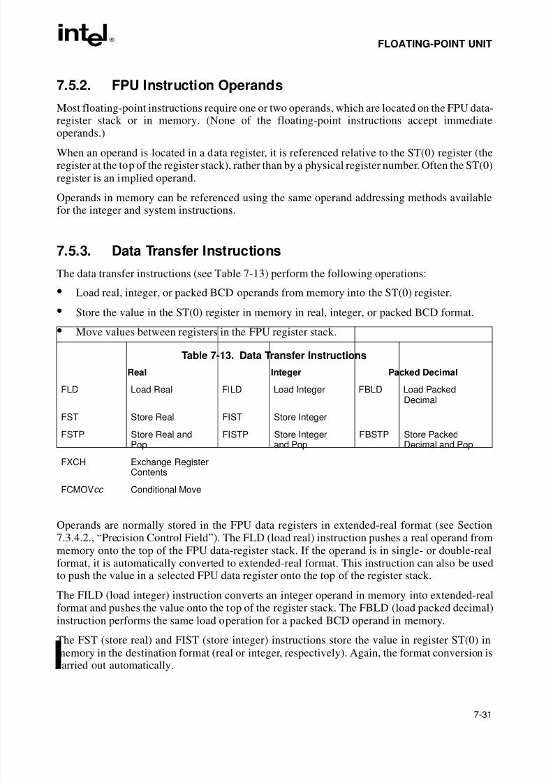
8/3/2019 Intel Architecture Software Developer's Manual, Volume 1: Basic Architecture
http://slidepdf.com/reader/full/intel-architecture-software-developers-manual-volume-1-basic-architecture 167/283
7-31
FLOATING-POINT UNIT
7.5.2. FPU Instruction Operands
Most floating-point instructions require one or two operands, which are located on the FPU data-register stack or in memory. (None of the floating-point instructions accept immediate
operands.)
When an operand is located in a data register, it is referenced relative to the ST(0) register (theregister at the top of the register stack), rather than by a physical register number. Often the ST(0)register is an implied operand.
Operands in memory can be referenced using the same operand addressing methods availablefor the integer and system instructions.
7.5.3. Data Transfer Instructions
The data transfer instructions (see Table 7-13) perform the following operations:
• Load real, integer, or packed BCD operands from memory into the ST(0) register.
• Store the value in the ST(0) register in memory in real, integer, or packed BCD format.
• Move values between registers in the FPU register stack.
Operands are normally stored in the FPU data registers in extended-real format (see Section
7.3.4.2., “Precision Control Field”). The FLD (load real) instruction pushes a real operand frommemory onto the top of the FPU data-register stack. If the operand is in single- or double-realformat, it is automatically converted to extended-real format. This instruction can also be usedto push the value in a selected FPU data register onto the top of the register stack.
The FILD (load integer) instruction converts an integer operand in memory into extended-realformat and pushes the value onto the top of the register stack. The FBLD (load packed decimal)instruction performs the same load operation for a packed BCD operand in memory.
The FST (store real) and FIST (store integer) instructions store the value in register ST(0) inmemory in the destination format (real or integer, respectively). Again, the format conversion iscarried out automatically.
Table 7-13. Data Transfer Instructions
Real Integer Packed Decimal
FLD Load Real FILD Load Integer FBLD Load Packed
DecimalFST Store Real FIST Store Integer
FSTP Store Real andPop
FISTP Store Integerand Pop
FBSTP Store PackedDecimal and Pop
FXCH Exchange RegisterContents
FCMOVcc Conditional Move
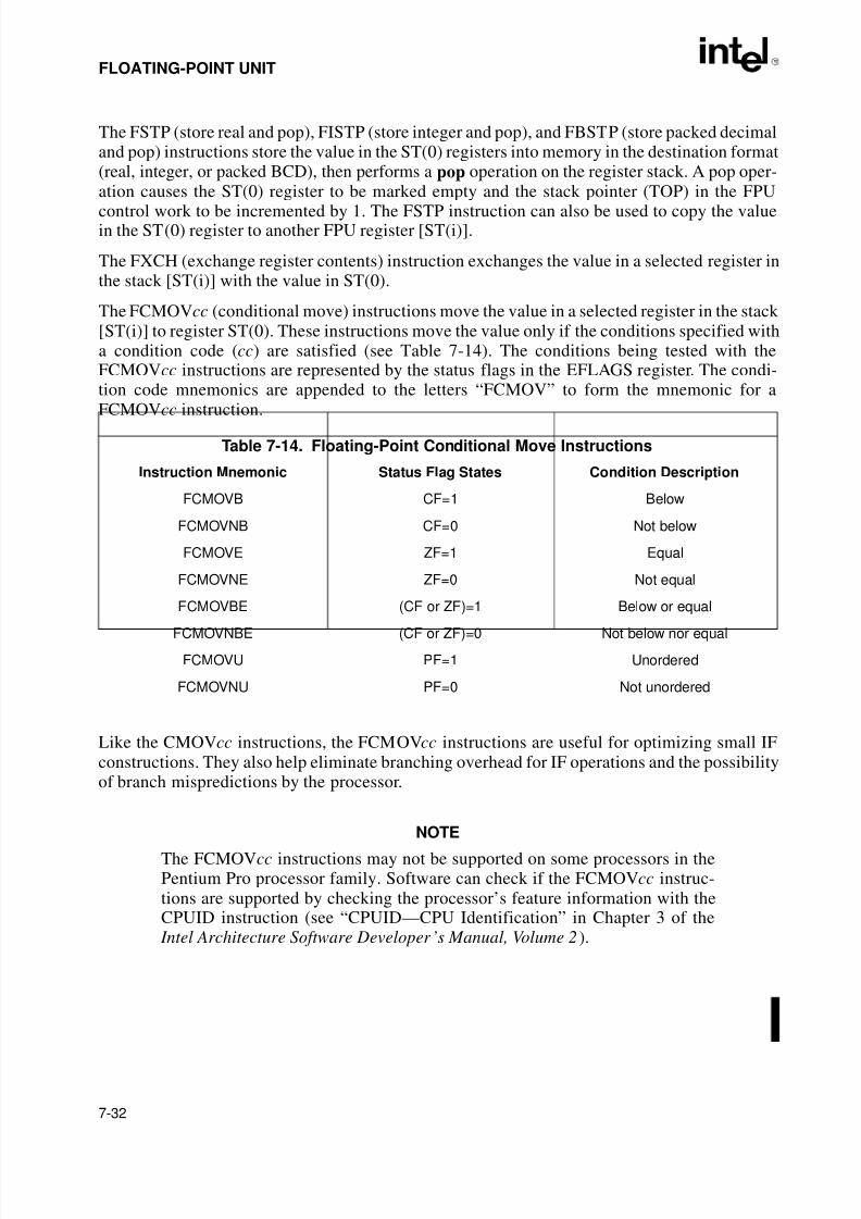
8/3/2019 Intel Architecture Software Developer's Manual, Volume 1: Basic Architecture
http://slidepdf.com/reader/full/intel-architecture-software-developers-manual-volume-1-basic-architecture 168/283
7-32
FLOATING-POINT UNIT
The FSTP (store real and pop), FISTP (store integer and pop), and FBSTP (store packed decimaland pop) instructions store the value in the ST(0) registers into memory in the destination format(real, integer, or packed BCD), then performs a pop operation on the register stack. A pop oper-ation causes the ST(0) register to be marked empty and the stack pointer (TOP) in the FPU
control work to be incremented by 1. The FSTP instruction can also be used to copy the valuein the ST(0) register to another FPU register [ST(i)].
The FXCH (exchange register contents) instruction exchanges the value in a selected register inthe stack [ST(i)] with the value in ST(0).
The FCMOVcc (conditional move) instructions move the value in a selected register in the stack [ST(i)] to register ST(0). These instructions move the value only if the conditions specified witha condition code (cc) are satisfied (see Table 7-14). The conditions being tested with theFCMOVcc instructions are represented by the status flags in the EFLAGS register. The condi-tion code mnemonics are appended to the letters “FCMOV” to form the mnemonic for a
FCMOVcc instruction.
Like the CMOVcc instructions, the FCMOVcc instructions are useful for optimizing small IFconstructions. They also help eliminate branching overhead for IF operations and the possibilityof branch mispredictions by the processor.
NOTEThe FCMOVcc instructions may not be supported on some processors in thePentium Pro processor family. Software can check if the FCMOVcc instruc-tions are supported by checking the processor’s feature information with theCPUID instruction (see “CPUID—CPU Identification” in Chapter 3 of the
Intel Architecture Software Developer’s Manual, Volume 2).
Table 7-14. Floating-Point Conditional Move Instructions
Instruction Mnemonic Status Flag States Condition Description
FCMOVB CF=1 Below
FCMOVNB CF=0 Not below
FCMOVE ZF=1 Equal
FCMOVNE ZF=0 Not equal
FCMOVBE (CF or ZF)=1 Below or equal
FCMOVNBE (CF or ZF)=0 Not below nor equal
FCMOVU PF=1 Unordered
FCMOVNU PF=0 Not unordered
8/3/2019 Intel Architecture Software Developer's Manual, Volume 1: Basic Architecture
http://slidepdf.com/reader/full/intel-architecture-software-developers-manual-volume-1-basic-architecture 169/283
7-33
FLOATING-POINT UNIT
7.5.4. Load Constant Instructions
The following instructions push commonly used constants onto the top [ST(0)] of the FPUregister stack:
FLDZ Load +0.0FLD1 Load +1.0FLDPI Load πFLDL2T Load log2 10FLDL2E Load log2eFLDLG2 Load log102FLDLN2 Load loge2
The constant values have full extended-real precision (64 bits) and are accurate to approximately19 decimal digits. They are stored internally in a format more precise than extended real. Whenloading the constant, the FPU rounds the more precise internal constant according to the RC(rounding control) field of the FPU control word. See Section 7.5.8., “Pi”, for information onthe π constant.
7.5.5. Basic Arithmetic Instructions
The following floating-point instructions perform basic arithmetic operations on real numbers.Where applicable, these instructions match IEEE Standard 754:
FADD/FADDP Add realFIADD Add integer to real
FSUB/FSUBP Subtract realFISUB Subtract integer from realFSUBR/FSUBRP Reverse subtract realFISUBR Reverse subtract real from integerFMUL/FMULP Multiply realFIMUL Multiply integer by realFDIV/FDIVP Divide realFIDIV Divide real by integerFDIVR/FDIVRP Reverse divideFIDIVR Reverse divide integer by real
FABS Absolute valueFCHS Change signFSQRT Square rootFPREM Partial remainderFPREM1 IEEE partial remainderFRNDINT Round to integral valueFXTRACT Extract exponent and significand
The add, subtract, multiply and divide instructions operate on the following types of operands:
• Two FPU register values.
• A register value and a real or integer value in memory.
8/3/2019 Intel Architecture Software Developer's Manual, Volume 1: Basic Architecture
http://slidepdf.com/reader/full/intel-architecture-software-developers-manual-volume-1-basic-architecture 170/283
7-34
FLOATING-POINT UNIT
Operands in memory can be in single-real, double-real, short-integer, or word-integer format.They are converted to extended-real format automatically.
Reverse versions of the subtract and divide instructions are provided to foster efficient coding.
For example, the FSUB instruction subtracts the value in a specified FPU register [ST(i)] fromthe value in register ST(0); whereas, the FSUBR instruction subtracts the value in ST(0) fromthe value in ST(i). The results of both operations are stored in register ST(0). These instructionseliminate the need to exchange values between register ST(0) and another FPU register toperform a subtraction or division.
The pop versions of the add, subtract, multiply and divide instructions pop the FPU register stack following the arithmetic operation.
The FPREM instruction computes the remainder from the division of two operands in themanner used by the Intel 8087 and Intel 287 math coprocessors; the FPREM1 instructionscomputes the remainder is the manner specified in the IEEE specification.
The FSQRT instruction computes the square root of the source operand.
The FRNDINT instructions rounds a real value to its nearest integer value, according to thecurrent rounding mode specified in the RC field of the FPU control word. This instructionperforms a function similar to the FIST/FISTP instructions, except that the result is saved in areal format.
The FABS, FCHS, and FXTRACT instructions perform convenient arithmetic operations. TheFABS instruction produces the absolute value of the source operand. The FCHS instructionchanges the sign of the source operand. The FXTRACT instruction separates the source operandinto its exponent and fraction and stores each value in a register in real format.
7.5.6. Comparison and Classification Instructions
The following instructions compare or classify real values:
FCOM/FCOMP/FCOMPP Compare real and set FPU condition code flags.FUCOM/FUCOMP/FUCOMPP Unordered compare real and set FPU condition code flags.FICOM/FICOMP Compare integer and set FPU condition code flags.FCOMI/FCOMIP Compare real and set EFLAGS status flags.FUCOMI/FUCOMIP Unordered compare real and set EFLAGS status flags.
FTST Test (compare real with 0.0).FXAM Examine.
Comparison of real values differ from comparison of integers because real values have four(rather than three) mutually exclusive relationships: less than, equal, greater than, andunordered.
The unordered relationship is true when at least one of the two values being compared is a NaNor in an undefined format. This additional relationship is required because, by definition, NaNsare not numbers, so they cannot have less than, equal, or greater than relationships with otherreal values.
8/3/2019 Intel Architecture Software Developer's Manual, Volume 1: Basic Architecture
http://slidepdf.com/reader/full/intel-architecture-software-developers-manual-volume-1-basic-architecture 171/283
8/3/2019 Intel Architecture Software Developer's Manual, Volume 1: Basic Architecture
http://slidepdf.com/reader/full/intel-architecture-software-developers-manual-volume-1-basic-architecture 172/283
7-36
FLOATING-POINT UNIT
unordered condition is the result of one or both of the operands being a QNaN. The FCOMIPand FUCOMIP instructions pop the FPU register stack following the comparison operation.
The FXAM instruction determines the classification of the real value in the ST(0) register (that
is, whether the value is zero, a denormal number, a normal finite number,∞, a NaN, or an unsup-ported format) or that the register is empty. It sets the FPU condition code flags to indicate theclassification (see “FXAM—Examine” in Chapter 3, Instruction Set Reference, of the Intel
Architecture Software Developer’s Manual, Volume 2). It also sets the C1 flag to indicate the signof the value.
7.5.6.1. BRANCHING ON THE FPU CONDITION CODES
The processor does not offer any control-flow instructions that branch on the setting of thecondition code flags (C0, C2, and C3) in the FPU status word. To branch on the state of theseflags, the FPU status word must first be moved to the AX register in the integer unit. The FSTSW
AX (store status word) instruction can be used for this purpose. When these flags are in the AXregister, the TEST instruction can be used to control conditional branching as follows:
1. Check for an unordered result. Use the TEST instruction to compare the contents of theAX register with the constant 0400H (see Table 7-17). This operation will clear the ZF flagin the EFLAGS register if the condition code flags indicate an unordered result; otherwise,the ZF flag will be set. The JNZ instruction can then be used to transfer control (if necessary) to a procedure for handling unordered operands.
2. Check ordered comparison result. Use the constants given in Table 7-17 in the TESTinstruction to test for a less than, equal to, or greater than result, then use the correspondingconditional branch instruction to transfer program control to the appropriate procedure or
section of code.
If a program or procedure has been thoroughly tested and it incorporates periodic checks forQNaN results, then it is not necessary to check for the unordered result every time a comparisonis made.
See Section 7.3.3., “Branching and Conditional Moves on FPU Condition Codes”, for anothertechnique for branching on FPU condition codes.
Some non-comparison FPU instructions update the condition code flags in the FPU status word.To ensure that the status word is not altered inadvertently, store it immediately following acomparison operation.
Table 7-17. TEST Instruction Constants for Conditional Branching
Order Constant Branch
ST(0) > Source Operand 4500H JZ
ST(0) < Source Operand 0100H JNZ
ST(0) = Source Operand 4000H JNZ
Unordered 0400H JNZ
8/3/2019 Intel Architecture Software Developer's Manual, Volume 1: Basic Architecture
http://slidepdf.com/reader/full/intel-architecture-software-developers-manual-volume-1-basic-architecture 173/283
7-37
FLOATING-POINT UNIT
7.5.7. Trigonometric Instructions
The following instructions perform four common trigonometric functions:
FSIN SineFCOS CosineFSINCOS Sine and cosineFPTAN TangentFPATAN Arctangent
These instructions operate on the top one or two registers of the FPU register stack and theyreturn their results to the stack. The source operands must be given in radians.
The FSINCOS instruction returns both the sine and the cosine of a source operand value. It oper-ates faster than executing the FSIN and FCOS instructions in succession.
The FPATAN instruction computes the arctangent of ST(1) divided by ST(0). It is useful forconverting rectangular coordinates to polar coordinates.
7.5.8. Pi
When the argument (source operand) of a trigonometric function is within the range of the func-tion, the argument is automatically reduced by the appropriate multiple of 2π through the samereduction mechanism used by the FPREM and FPREM1 instructions. The internal value of πthat the Intel Architecture FPU uses for argument reduction and other computations is asfollows:
π = 0.f ∗ 22
where:
f = C90FDAA2 2168C234 C
(The spaces in the fraction above indicate 32-bit boundaries.)
This internal π value has a 66-bit mantissa, which is 2 bits more than is allowed in the significandof an extended-real value. (Since 66 bits is not an even number of hexadecimal digits, two addi-tional zeros have been added to the value so that it can be represented in hexadecimalformat. The least-significant hexadecimal digit (C) is thus 1100B, where the two least-
significant bits represent bits 67 and 68 of the mantissa.)
This value of π has been chosen to guarantee no loss of significance in a source operand,provided the operand is within the specified range for the instruction.
If the results of computations that explicitly use π are to be used in the FSIN, FCOS, FSINCOS,or FPTAN instructions, the full 66-bit fraction of π should be used. This insures that the resultsare consistent with the argument-reduction algorithms that these instructions use. Using arounded version of π can cause inaccuracies in result values, which if propagated through severalcalculations, might result in meaningless results.
8/3/2019 Intel Architecture Software Developer's Manual, Volume 1: Basic Architecture
http://slidepdf.com/reader/full/intel-architecture-software-developers-manual-volume-1-basic-architecture 174/283
7-38
FLOATING-POINT UNIT
A common method of representing the full 66-bit fraction of π is to separate the value into twonumbers (highπ and lowπ) that when added together give the value for π shown earlier in thissection with the full 66-bit fraction:
π = highπ + lowπFor example, the following two values (given in scientific notation with the fraction in hexadec-imal and the exponent in decimal) represent the 33 most-significant and the 33 least-significantbits of the fraction:
highπ (unnormalized)= 0.C90FDAA20 * 2+2
lowπ (unnormalized)= 0.42D184698 * 2−31
These values encoded in standard IEEE double-real format are as follows:
highπ = 400921FB 54400000
lowπ = 3DE0B461 1A600000
(Note that in the IEEE double-real format, the exponents are biased (by 1023) and the fractionsare normalized.)
Similar versions of π can also be written in extended-real format.
When using this two-part π value in an algorithm, parallel computations should be performedon each part, with the results kept separate. When all the computations are complete, the tworesults can be added together to form the final result.
The complications of maintaining a consistent value of π for argument reduction can be avoided,
either by applying the trigonometric functions only to arguments within the range of theautomatic reduction mechanism, or by performing all argument reductions (down to a magni-tude less than π /4) explicitly in software.
7.5.9. Logarithmic, Exponential, and Scale
The following instructions provide two different logarithmic functions, an exponential function,and a scale function.
FYL2X Compute log (y ∗ log2x)
FYL2XP1 Compute log epsilon (y ∗ log2(x + 1))F2XM1 Compute exponential (2x – 1)FSCALE Scale
The FYL2X and FYL2XP1 instructions perform two different base 2 logarithmic operations.The FYL2X instruction computes the log of (y ∗ log2x). This operation permits the calculationof the log of any base using the following equation:
logb x = (1/log2 b) ∗ log2 x
The FYL2XP1 instruction computes the log epsilon of (y ∗ log2 (x + 1)). This operation providesoptimum accuracy for values of epsilon (ε) that are close to 0.
8/3/2019 Intel Architecture Software Developer's Manual, Volume 1: Basic Architecture
http://slidepdf.com/reader/full/intel-architecture-software-developers-manual-volume-1-basic-architecture 175/283
7-39
FLOATING-POINT UNIT
The F2XM1 instruction computes the exponential (2x − 1). This instruction only operates onsource values in the range −1.0 to +1.0.
The FSCALE instruction multiplies the source operand by a power of 2.
7.5.10. Transcendental Instruction Accuracy
The algorithms that the Pentium and Pentium Pro processors use for the transcendental instruc-tions (FSIN, FCOS, FSINCOS, FPTAN, FPATAN, F2XM1, FYL2X, and FYL2XP1) allow ahigher level of accuracy than was possible in earlier Intel Architecture math coprocessors andFPUs. The accuracy of these instructions is measured in terms of units in the last place (ulp).For a given argument x, let f ( x) and F ( x) be the correct and computed (approximate) functionvalues, respectively. The error in ulps is defined to be:
where k is an integer such that .
With the Pentium and Pentium Pro processors, the worst case error on transcendental func-tions is less than 1 ulp when rounding to the nearest-even and less than 1.5 ulps when roundingin other modes. The functions are guaranteed to be monotonic, with respect to the input oper-ands, throughout the domain supported by the instruction.
With the Intel486 processor and Intel 387 math coprocessor, the worst-case, transcendental-
function error is typically 3 or 3.5 ulps, but is sometimes as large as 4.5 ulps.
7.5.11. FPU Control Instructions
The following instructions control the state and modes of operation of the FPU. They also allowthe status of the FPU to be examined:
FINIT/FNINIT Initialize FPUFLDCW Load FPU control wordFSTCW/FNSTCW Store FPU control word
FSTSW/FNSTSW Store FPU status wordFCLEX/FNCLEX Clear FPU exception flagsFLDENV Load FPU environmentFSTENV/FNSTENV Store FPU environmentFRSTOR Restore FPU stateFSAVE/FNSAVE Save FPU stateFINCSTP Increment FPU register stack pointerFDECSTP Decrement FPU register stack pointerFFREE Free FPU registerFNOP No operationWAIT/FWAIT Check for and handle pending unmasked FPU exceptions
error f x( ) F x( )–2
k 63–-------------------------------=
1 2k –
f x( ) 2<≤
8/3/2019 Intel Architecture Software Developer's Manual, Volume 1: Basic Architecture
http://slidepdf.com/reader/full/intel-architecture-software-developers-manual-volume-1-basic-architecture 176/283
7-40
FLOATING-POINT UNIT
The FINIT/FNINIT instructions initialize the FPU and its internal registers to default values.
The FLDCW instructions loads the FPU control word register with a value from memory. TheFSTCW/FNSTCW and FSTSW/FNSTSW instructions store the FPU control and status words,
respectively, in memory (or for an FSTSW/FNSTSW instruction in a general-purpose register).The FSTENV/FNSTENV and FSAVE/FNSAVE instructions save the FPU environment andstate, respectively, in memory. The FPU environment includes all the FPU’s control and statusregisters; the FPU state includes the FPU environment and the data registers in the FPU registerstack. (The FSAVE/FNSAVE instruction also initializes the FPU to default values, like theFINIT/FNINIT instruction, after it saves the original state of the FPU.)
The FLDENV and FRSTOR instructions load the FPU environment and state, respectively, frommemory into the FPU. These instructions are commonly used when switching tasks or contexts.
The WAIT/FWAIT instructions are synchronization instructions. (They are actually mnemonics
for the same opcode.) These instructions check the FPU status word for pending unmasked FPUexceptions. If any pending unmasked FPU exceptions are found, they are handled before theprocessor resumes execution of the instructions (integer, floating-point, or system instruction)in the instruction stream. The WAIT/FWAIT instructions are provided to allow synchronizationof instruction execution between the FPU and the processor’s integer unit. See Section 7.9.,“Floating-Point Exception Synchronization” for more information on the use of theWAIT/FWAIT instructions.
7.5.12. Waiting Vs. Non-waiting Instructions
All of the floating-point instructions except a few special control instructions perform a waitoperation (similar to the WAIT/FWAIT instructions), to check for and handle pending unmaskedFPU exceptions, before they perform their primary operation (such as adding two real numbers).These instructions are called waiting instructions. Some of the FPU control instructions, suchas FSTSW/FNSTSW, have both a waiting and a non-waiting versions. The waiting version (withthe “F” prefix) executes a wait operation before it performs its primary operation; whereas, thenon-waiting version (with the “FN” prefix) ignores pending unmasked exceptions. Non-waitinginstructions allow software to save the current FPU state without first handling pending excep-tions or to reset or reinitialize the FPU without regard for pending exceptions.
NOTE
When operating a Pentium or Intel486 processor in MS-DOS compatibilitymode, it is possible (under unusual circumstances) for a non-waitinginstruction to be interrupted prior to being executed to handle a pending FPUexception. The circumstances where this can happen and the resulting actionof the processor are described in Section D.2.1.3., “No-Wait FPU InstructionsCan Get FPU Interrupt in Window”. When operating a Pentium Pro processorin MS-DOS compatibility mode, non-waiting instructions can not beinterrupted in this way (see Section D.2.2., “MS-DOS* Compatibility Modein the Pentium® Pro Processor”).
8/3/2019 Intel Architecture Software Developer's Manual, Volume 1: Basic Architecture
http://slidepdf.com/reader/full/intel-architecture-software-developers-manual-volume-1-basic-architecture 177/283
8/3/2019 Intel Architecture Software Developer's Manual, Volume 1: Basic Architecture
http://slidepdf.com/reader/full/intel-architecture-software-developers-manual-volume-1-basic-architecture 178/283
7-42
FLOATING-POINT UNIT
7.6.1. Uses for Signaling NANs
By unmasking the invalid operation exception, the programmer can use signaling NaNs to trapto the exception handler. The generality of this approach and the large number of NaN values
that are available provide the sophisticated programmer with a tool that can be applied to avariety of special situations.
For example, a compiler can use signaling NaNs as references to uninitialized (real) arrayelements. The compiler can preinitialize each array element with a signaling NaN whose signif-icand contained the index (relative position) of the element. Then, if an application programattempts to access an element that it had not initialized, it can use the NaN placed there by thecompiler. If the invalid operation exception is unmasked, an interrupt will occur, and the excep-tion handler will be invoked. The exception handler can determine which element has beenaccessed, since the operand address field of the exception pointers will point to the NaN, and theNaN will contain the index number of the array element.
7.6.2. Uses for Quiet NANs
Quiet NaNs are often used to speed up debugging. In its early testing phase, a program oftencontains multiple errors. An exception handler can be written to save diagnostic information inmemory whenever it was invoked. After storing the diagnostic data, it can supply a quiet NaNas the result of the erroneous instruction, and that NaN can point to its associated diagnostic areain memory. The program will then continue, creating a different NaN for each error. When theprogram ends, the NaN results can be used to access the diagnostic data saved at the time theerrors occurred. Many errors can thus be diagnosed and corrected in one test run.
In embedded applications which use computed results in further computations, an undetectedQNaN can invalidate all subsequent results. Such applications should therefore periodicallycheck for QNaNs and provide a recovery mechanism to be used if a QNaN result is detected.
7.7. FLOATING-POINT EXCEPTION HANDLING
The FPU detects six classes of exception conditions while executing floating-point instructions:
• Invalid operation (#I)
— Stack overflow or underflow (#IS)
— Invalid arithmetic operation (#IA)
• Divide-by-zero (#Z)
• Denormalized operand (#D)
• Numeric overflow (#O)
• Numeric underflow (#U)
• Inexact result (precision) (#P)
8/3/2019 Intel Architecture Software Developer's Manual, Volume 1: Basic Architecture
http://slidepdf.com/reader/full/intel-architecture-software-developers-manual-volume-1-basic-architecture 179/283
7-43
FLOATING-POINT UNIT
The nomenclature of “#” symbol followed by one or two letters (for example, #IS) is used in thismanual to indicate exception conditions. It is merely a short-hand form and is not related toassembler mnemonics.
Each of the six exception classes has a corresponding flag bit in the FPU status word and a mask bit in the FPU control word (see Section 7.3.2., “FPU Status Register” and Section 7.3.4., “FPUControl Word”, respectively). In addition, the exception summary (ES) flag in the status wordindicates when any of the exceptions has been detected, and the stack fault (SF) flag (also in thestatus word) distinguishes between the two types of invalid-operation exceptions.
When the FPU detects a floating-point exception, it sets the appropriate flags in the FPU statusword, then takes one of two possible courses of action:
• Handles the exception automatically, producing a predefined (and often times usableresult), while allowing program execution to continue undisturbed.
• Invokes a software exception handler to handle the exception.The following sections describe how the FPU handles exceptions (either automatically or bycalling a software exception handler), how the FPU detects the various floating-point excep-tions, and the automatic (masked) response to the floating-point exceptions.
7.7.1. Arithmetic vs. Non-arithmetic Instructions
When dealing with floating-point exceptions, it is useful to distinguish between arithmeticinstructions and non-arithmetic instructions. Non-arithmetic instructions have no operands
or do not make substantial changes to their operands. Arithmetic instructions do make signifi-cant changes to their operands; in particular, they make changes that could result in a floating-point exception being signaled. Table 7-19 lists the non-arithmetic and arithmetic instructions.It should be noted that some non-arithmetic instructions can signal a floating-point stack (fault)exception, but this exception is not the result of an operation on an operand.
7.7.2. Automatic Exception Handling
If the FPU detects an exception condition for a masked exception (an exception with its mask bit set), it sets the exception flag for the exception and delivers a predefined (default) response
and continues executing instructions. The masked (default) responses to exceptions have beenchosen to deliver a reasonable result for each exception condition and are generally satisfactoryfor most floating-point applications. By masking or unmasking specific floating-point excep-tions in the FPU control word, programmers can delegate responsibility for most exceptions tothe FPU and reserve the most severe exception conditions for software exception handlers.
Because the exception flags are “sticky,” they provide a cumulative record of the exceptions thathave occurred since they were last cleared. A programmer can thus mask all exceptions, run acalculation, and then inspect the exception flags to see if any exceptions were detected duringthe calculation.
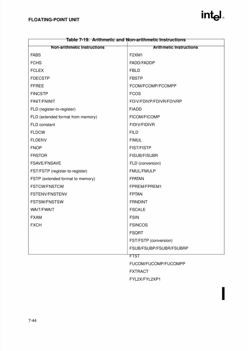
8/3/2019 Intel Architecture Software Developer's Manual, Volume 1: Basic Architecture
http://slidepdf.com/reader/full/intel-architecture-software-developers-manual-volume-1-basic-architecture 180/283
7-44
FLOATING-POINT UNIT
Table 7-19. Arithmetic and Non-arithmetic Instructions
Non-arithmetic Instructions Arithmetic Instructions
FABS F2XM1
FCHS FADD/FADDP
FCLEX FBLD
FDECSTP FBSTP
FFREE FCOM/FCOMP/FCOMPP
FINCSTP FCOS
FINIT/FNINIT FDIV/FDIVP/FDIVR/FDIVRP
FLD (register-to-register) FIADD
FLD (extended format from memory) FICOM/FICOMP
FLD constant FIDIV/FIDIVR
FLDCW FILD
FLDENV FIMUL
FNOP FIST/FISTP
FRSTOR FISUB/FISUBR
FSAVE/FNSAVE FLD (conversion)
FST/FSTP (register-to-register) FMUL/FMULP
FSTP (extended format to memory) FPATANFSTCW/FNSTCW FPREM/FPREM1
FSTENV/FNSTENV FPTAN
FSTSW/FNSTSW FRNDINT
WAIT/FWAIT FSCALE
FXAM FSIN
FXCH FSINCOS
FSQRT
FST/FSTP (conversion)
FSUB/FSUBP/FSUBR/FSUBRP
FTST
FUCOM/FUCOMP/FUCOMPP
FXTRACT
FYL2X/FYL2XP1
8/3/2019 Intel Architecture Software Developer's Manual, Volume 1: Basic Architecture
http://slidepdf.com/reader/full/intel-architecture-software-developers-manual-volume-1-basic-architecture 181/283

8/3/2019 Intel Architecture Software Developer's Manual, Volume 1: Basic Architecture
http://slidepdf.com/reader/full/intel-architecture-software-developers-manual-volume-1-basic-architecture 182/283
7-46
FLOATING-POINT UNIT
2. If the IGNNE# pin is deasserted, the FPU then asserts the FERR# pin either immediately,or else delayed (deferred) until just before the execution of the next waiting floating-pointinstruction or MMX™ instruction. Whether the FERR# pin is asserted immediately ordelayed depends on the type of processor, the instruction, and the type of exception.
3. If a preceding floating-point instruction has set the exception flag for an unmasked FPUexception, the processor freezes just before executing the next WAIT instruction, waitingfloating-point instruction, or MMX instruction. Whether the FERR# pin was asserted atthe preceding floating-point instruction or is just now being asserted, the freezing of theprocessor assures that the FPU exception handler will be invoked before the new floating-point (or MMX) instruction gets executed.
4. The FERR# pin is connected through external hardware to IRQ13 of a cascaded, program-mable interrupt controller (PIC). When the FERR# pin is asserted, the PIC is programmedto generate an interrupt 75H.
5. The PIC asserts the INTR pin on the processor to signal the interrupt 75H.
6. The BIOS for the PC system handles the interrupt 75H by branching to the interrupt 2(NMI) interrupt handler.
7. The interrupt 2 handler determines if the interrupt is the result of an NMI interrupt or afloating-point exception.
8. If a floating-point exception is detected, the interrupt 2 handler branches to the floating-point exception handler.
If the IGNNE# pin is asserted, the processor ignores floating-point error conditions. This pin is
provided to inhibit floating-point exceptions from being generated while the floating-pointexception handler is servicing a previously signaled floating-point exception.
Appendix D, Guidelines for Writing FPU Exception Handlers, describes the MS-DOS compat-ibility mode in much greater detail. This mode is somewhat more complicated in the Intel486and Pentium processor implementations, as described in Appendix D.
7.7.3.3. TYPICAL FLOATING-POINT EXCEPTION HANDLER ACTIONS
After the floating-point exception handler is invoked, the processor handles the exception in thesame manner that it handles non-FPU exceptions. (The floating-point exception handler is
normally part of the operating system or executive software.) A typical action of the exceptionhandler is to store FPU state information in memory (with the FSTENV/FNSTENV orFSAVE/FNSAVE instructions) so that it can evaluate the exception and formulate an appropriateresponse (see Section 7.3.9., “Saving the FPU’s State”). Other typical exception handler actionsinclude:
• Examining stored FPU state information (control, status, and tag words, and FPUinstruction and operand pointers) to determine the nature of the error.
• Correcting the condition that caused the error.
• Clearing the exception bits in the status word.
• Returning to the interrupted program and resuming normal execution.
8/3/2019 Intel Architecture Software Developer's Manual, Volume 1: Basic Architecture
http://slidepdf.com/reader/full/intel-architecture-software-developers-manual-volume-1-basic-architecture 183/283
7-47
FLOATING-POINT UNIT
If the faulting floating-point instruction is followed by one or more non-floating-point instruc-tions, it may not be useful to re-execute the faulting instruction. See Section 7.9., “Floating-Point Exception Synchronization”, for more information on synchronizing floating-point excep-tions.
In cases where the handler needs to restart program execution with the faulting instruction, theIRET instruction cannot be used directly. The reason for this is that because the exception is notgenerated until the next floating-point or WAIT/FWAIT instruction following the faultingfloating-point instruction, the return instruction pointer on the stack may not point to the faultinginstruction. To restart program execution at the faulting instruction, the exception handler mustobtain a pointer to the instruction from the saved FPU state information, load it into the returninstruction pointer location on the stack, and then execute the IRET instruction.
In lieu of writing recovery procedures, the exception handler can do the following:
• Increment an exception counter for later display or printing.
• Print or display diagnostic information (such as, the FPU environment and registers).
• Halt further program execution.
See Section D.3.4., “FPU Exception Handling Examples”, for general examples of floating-point exception handlers and for specific examples of how to write a floating-point exceptionhandler when using the MS-DOS compatibility mode.
7.8. FLOATING-POINT EXCEPTION CONDITIONS
The following sections describe the various conditions that cause a floating-point exception tobe generated and the masked response of the FPU when these conditions are detected. Chapter3, Instruction Set Reference, in the Intel Architecture Software Developer’s Manual, Volume 2,lists the floating-point exceptions that can be signaled for each floating-point instruction.
7.8.1. Invalid Operation Exception
The floating-point invalid-operation exception occurs in response to two general types of oper-ations:
• Stack overflow or underflow (#IS).• Invalid arithmetic operand (#IA).
The flag for this exception (IE) is bit 0 of the FPU status word, and the mask bit (IM) is bit 0 of the FPU control word. The stack fault flag (SF) of the FPU status word indicates the type of operation caused the exception. When the SF flag is set to 1, a stack operation has resulted instack overflow or underflow; when the flag is cleared to 0, an arithmetic instruction has encoun-tered an invalid operand. Note that the FPU explicitly sets the SF flag when it detects a stack overflow or underflow condition, but it does not explicitly clear the flag when it detects aninvalid-arithmetic-operand condition. As a result, the state of the SF flag can be 1 following aninvalid-arithmetic-operation exception, if it was not cleared from the last time a stack overflow
or underflow condition occurred. See Section 7.3.2.4., “Stack Fault Flag”, for more informationabout the SF flag.
8/3/2019 Intel Architecture Software Developer's Manual, Volume 1: Basic Architecture
http://slidepdf.com/reader/full/intel-architecture-software-developers-manual-volume-1-basic-architecture 184/283
7-48
FLOATING-POINT UNIT
7.8.1.1. STACK OVERFLOW OR UNDERFLOW EXCEPTION (#IS)
The FPU tag word keeps track of the contents of the registers in the FPU register stack (seeSection 7.3.6., “FPU Tag Word”). It then uses this information to detect two different types of
stack faults:• Stack overflow—an instruction attempts to write a value into a non-empty FPU register
• Stack underflow—an instruction attempts to read a value from an empty FPU register.
When the FPU detects stack overflow or underflow, it sets the IE flag (bit 0) and the SF flag (bit6) in the FPU status word to 1. It then sets condition-code flag C1 (bit 9) in the FPU status wordto 1 if stack overflow occurred or to 0 if stack underflow occurred.
If the invalid-operation exception is masked, the FPU then returns the real, integer, or BCD-integer indefinite value to the destination operand, depending on the instruction being executed.This value overwrites the destination register or memory location specified by the instruction.
If the invalid-operation exception is not masked, a software exception handler is invoked (seeSection 7.7.3., “Software Exception Handling”) and the top-of-stack pointer (TOP) and sourceoperands remain unchanged.
The term stack overflow comes from the condition where the a program has pushed eight valuesonto the FPU register stack and the next value pushed on the stack causes a stack wraparound toa register that already contains a value. The term stack underflow refers to the opposite conditionfrom stack overflow. Here, a program has popped eight values from the FPU register stack andthe next value popped from the stack causes stack wraparound to an empty register.
7.8.1.2. INVALID ARITHMETIC OPERAND EXCEPTION (#IA)
The FPU is able to detect a variety of invalid arithmetic operations that can be coded in aprogram. These operations generally indicate a programming error, such as dividing ∞ by ∞.Table 7-20 lists the invalid arithmetic operations that the FPU detects. This group includes theinvalid operations defined in IEEE Std. 854.
When the FPU detects an invalid arithmetic operand, it sets the IE flag (bit 0) in the FPU statusword to 1. If the invalid-operation exception is masked, the FPU then returns an indefinite valueto the destination operand or sets the floating-point condition codes, as shown in Table 7-20. If the invalid-operation exception is not masked, a software exception handler is invoked (see
Section 7.7.3., “Software Exception Handling”) and the top-of-stack pointer (TOP) and sourceoperands remain unchanged.
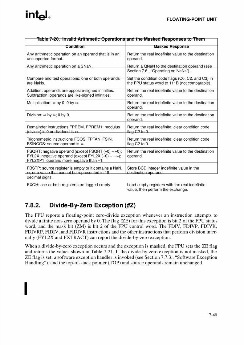
8/3/2019 Intel Architecture Software Developer's Manual, Volume 1: Basic Architecture
http://slidepdf.com/reader/full/intel-architecture-software-developers-manual-volume-1-basic-architecture 185/283
7-49
FLOATING-POINT UNIT
7.8.2. Divide-By-Zero Exception (#Z)
The FPU reports a floating-point zero-divide exception whenever an instruction attempts todivide a finite non-zero operand by 0. The flag (ZE) for this exception is bit 2 of the FPU statusword, and the mask bit (ZM) is bit 2 of the FPU control word. The FDIV, FDIVP, FDIVR,FDIVRP, FIDIV, and FIDIVR instructions and the other instructions that perform division inter-
nally (FYL2X and FXTRACT) can report the divide-by-zero exception.
When a divide-by-zero exception occurs and the exception is masked, the FPU sets the ZE flagand returns the values shown in Table 7-21. If the divide-by-zero exception is not masked, theZE flag is set, a software exception handler is invoked (see Section 7.7.3., “Software ExceptionHandling”), and the top-of-stack pointer (TOP) and source operands remain unchanged.
Table 7-20. Invalid Arithmetic Operations and the Masked Responses to Them
Condition Masked Response
Any arithmetic operation on an operand that is in an
unsupported format.
Return the real indefinite value to the destination
operand.
Any arithmetic operation on a SNaN. Return a QNaN to the destination operand (seeSection 7.6., “Operating on NaNs”).
Compare and test operations: one or both operandsare NaNs.
Set the condition code flags (C0, C2, and C3) inthe FPU status word to 111B (not comparable).
Addition: operands are opposite-signed infinities.Subtraction: operands are like-signed infinities.
Return the real indefinite value to the destinationoperand.
Multiplication: ∞ by 0; 0 by ∞. Return the real indefinite value to the destinationoperand.
Division: ∞ by ∞; 0 by 0. Return the real indefinite value to the destination
operand.
Remainder instructions FPREM, FPREM1: modulus(divisor) is 0 or dividend is ∞.
Return the real indefinite; clear condition codeflag C2 to 0.
Trigonometric instructions FCOS, FPTAN, FSIN,FSINCOS: source operand is ∞.
Return the real indefinite; clear condition codeflag C2 to 0.
FSQRT: negative operand (except FSQRT (–0) = –0);FYL2X: negative operand (except FYL2X (–0) = – ∞);FYL2XP1: operand more negative than –1.
Return the real indefinite value to the destinationoperand.
FBSTP: source register is empty or it contains a NaN,∞, or a value that cannot be represented in 18
decimal digits.
Store BCD integer indefinite value in thedestination operand.
FXCH: one or both registers are tagged empty. Load empty registers with the real indefinitevalue, then perform the exchange.
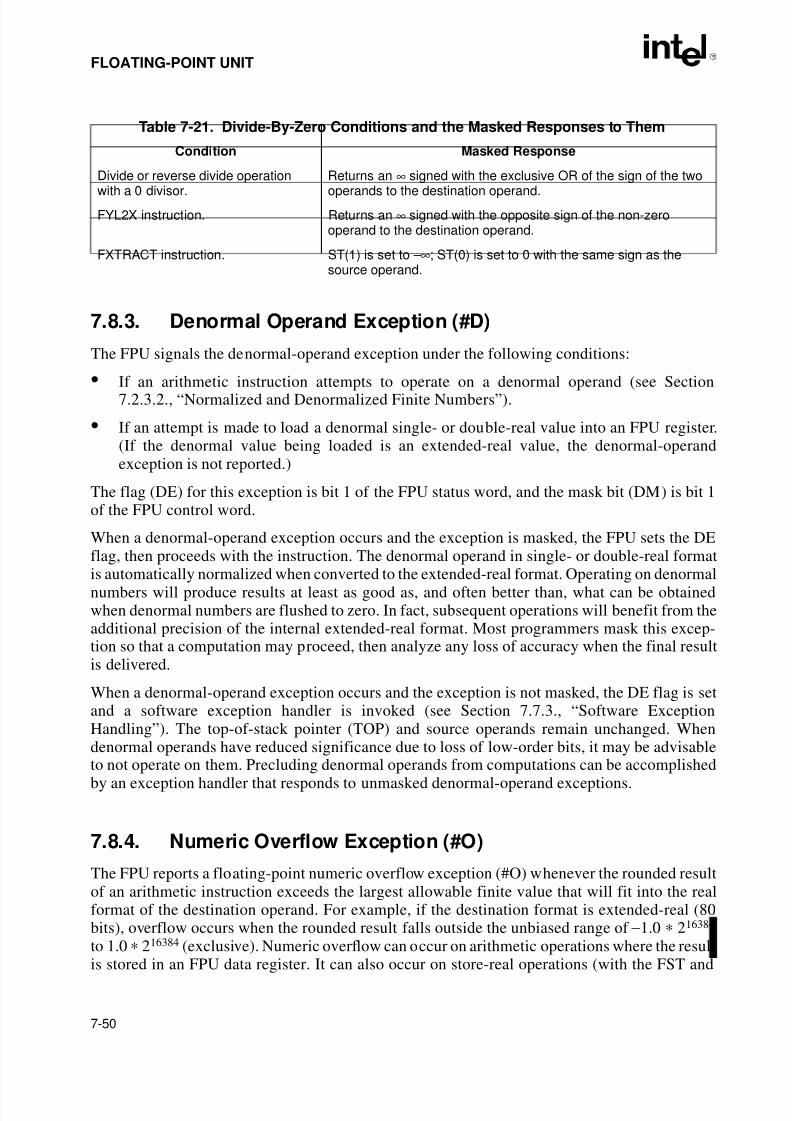
8/3/2019 Intel Architecture Software Developer's Manual, Volume 1: Basic Architecture
http://slidepdf.com/reader/full/intel-architecture-software-developers-manual-volume-1-basic-architecture 186/283
7-50
FLOATING-POINT UNIT
7.8.3. Denormal Operand Exception (#D)
The FPU signals the denormal-operand exception under the following conditions:
• If an arithmetic instruction attempts to operate on a denormal operand (see Section7.2.3.2., “Normalized and Denormalized Finite Numbers”).
• If an attempt is made to load a denormal single- or double-real value into an FPU register.(If the denormal value being loaded is an extended-real value, the denormal-operandexception is not reported.)
The flag (DE) for this exception is bit 1 of the FPU status word, and the mask bit (DM) is bit 1of the FPU control word.
When a denormal-operand exception occurs and the exception is masked, the FPU sets the DEflag, then proceeds with the instruction. The denormal operand in single- or double-real format
is automatically normalized when converted to the extended-real format. Operating on denormalnumbers will produce results at least as good as, and often better than, what can be obtainedwhen denormal numbers are flushed to zero. In fact, subsequent operations will benefit from theadditional precision of the internal extended-real format. Most programmers mask this excep-tion so that a computation may proceed, then analyze any loss of accuracy when the final resultis delivered.
When a denormal-operand exception occurs and the exception is not masked, the DE flag is setand a software exception handler is invoked (see Section 7.7.3., “Software ExceptionHandling”). The top-of-stack pointer (TOP) and source operands remain unchanged. Whendenormal operands have reduced significance due to loss of low-order bits, it may be advisable
to not operate on them. Precluding denormal operands from computations can be accomplishedby an exception handler that responds to unmasked denormal-operand exceptions.
7.8.4. Numeric Overflow Exception (#O)
The FPU reports a floating-point numeric overflow exception (#O) whenever the rounded resultof an arithmetic instruction exceeds the largest allowable finite value that will fit into the realformat of the destination operand. For example, if the destination format is extended-real (80bits), overflow occurs when the rounded result falls outside the unbiased range of −1.0 ∗ 216384
to 1.0 ∗ 216384 (exclusive). Numeric overflow can occur on arithmetic operations where the result
is stored in an FPU data register. It can also occur on store-real operations (with the FST and
Table 7-21. Divide-By-Zero Conditions and the Masked Responses to Them
Condition Masked Response
Divide or reverse divide operation
with a 0 divisor.
Returns an ∞ signed with the exclusive OR of the sign of the two
operands to the destination operand.
FYL2X instruction. Returns an ∞ signed with the opposite sign of the non-zerooperand to the destination operand.
FXTRACT instruction. ST(1) is set to – ∞; ST(0) is set to 0 with the same sign as thesource operand.
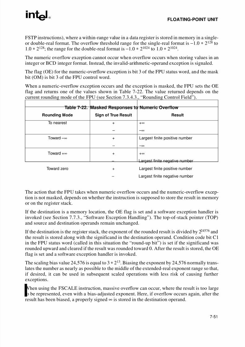
8/3/2019 Intel Architecture Software Developer's Manual, Volume 1: Basic Architecture
http://slidepdf.com/reader/full/intel-architecture-software-developers-manual-volume-1-basic-architecture 187/283
8/3/2019 Intel Architecture Software Developer's Manual, Volume 1: Basic Architecture
http://slidepdf.com/reader/full/intel-architecture-software-developers-manual-volume-1-basic-architecture 188/283
7-52
FLOATING-POINT UNIT
7.8.5. Numeric Underflow Exception (#U)
The FPU reports a floating-point numeric underflow exception (#U) whenever the roundedresult of an arithmetic instruction is “tiny” (that is, less than the smallest possible normalized,
finite value that will fit into the real format of the destination operand). For example, if the desti-nation format is extended-real (80 bits), underflow occurs when the rounded result falls in theunbiased range of −1.0 ∗ 2−16382 to 1.0 ∗ 2−16382 (exclusive). Like numeric overflow, numericunderflow can occur on arithmetic operations where the result is stored in an FPU data register.It can also occur on store-real operations (with the FST and FSTP instructions), where a within-range value in a data register is stored in memory in a single- or double-real format. The under-flow threshold range for the single-real format is −1.0 ∗ 2−126 to 1.0 ∗ 2−126; the range for thedouble-real format is −1.0 ∗ 2−1022 to 1.0 ∗ 2−1022. (The numeric underflow exception cannotoccur when storing values in an integer or BCD integer format.)
The flag (UE) for the numeric-underflow exception is bit 4 of the FPU status word, and the mask
bit (UM) is bit 4 of the FPU control word.
When a numeric-underflow exception occurs and the exception is masked, the FPU denormal-izes the result (see Section 7.2.3.2., “Normalized and Denormalized Finite Numbers”). If thedenormalized result is exact, the FPU stores the result in the destination operand, without settingthe UE flag. If the denormal result is inexact, the FPU sets the UE flag, then goes on to handlethe inexact-result exception condition (see Section 7.8.6., “Inexact-Result (Precision) Exception(#P)”). It is important to note that if numeric-underflow is masked, a numeric-underflow excep-tion is signaled only if the denormalized result is inexact. If the denormalized result is exact, noflags are set and no exceptions are signaled.
The action that the FPU takes when numeric underflow occurs and the numeric-underflow
exception is not masked, depends on whether the instruction is supposed to store the result inmemory or on the register stack.
If the destination is a memory location, the UE flag is set and a software exception handler isinvoked (see Section 7.7.3., “Software Exception Handling”). The top-of-stack pointer (TOP)and source and destination operands remain unchanged.
If the destination is the register stack, the exponent of the rounded result is multiplied by224576 and the product is stored along with the significand in the destination operand. Conditioncode bit C1 in the FPU the status register (acting here as a “round-up bit”) is set if the significandwas rounded upward and cleared if the result was rounded toward 0. After the result is stored,
the UE flag is set and a software exception handler is invoked.The scaling bias value 24,576 is the same as is used for the overflow exception and has the sameeffect, which is to translate the result as nearly as possible to the middle of the extended-realexponent range.
When using the FSCALE instruction, massive underflow can occur, where the result is too tinyto be represented, even with a bias-adjusted exponent. Here, if underflow occurs again, after theresult has been biased, a properly signed 0 is stored in the destination operand.
8/3/2019 Intel Architecture Software Developer's Manual, Volume 1: Basic Architecture
http://slidepdf.com/reader/full/intel-architecture-software-developers-manual-volume-1-basic-architecture 189/283
7-53
FLOATING-POINT UNIT
7.8.6. Inexact-Result (Precision) Exception (#P)
The inexact-result exception (also called the precision exception) occurs if the result of an oper-ation is not exactly representable in the destination format. For example, the fraction 1/3 cannot
be precisely represented in binary form. This exception occurs frequently and indicates thatsome (normally acceptable) accuracy has been lost. The exception is supported for applicationsthat need to perform exact arithmetic only. Because the rounded result is generally satisfactoryfor most applications, this exception is commonly masked. Note that the transcendental instruc-tions [FSIN, FCOS, FSINCOS, FPTAN, FPATAN, F2XM1, FYL2X, and FYL2XP1] by natureproduce inexact results.
The inexact-result exception flag (PE) is bit 5 of the FPU status word, and the mask bit (PM) isbit 5 of the FPU control word.
If the inexact-result exception is masked when an inexact-result condition occurs and a numeric
overflow or underflow condition has not occurred, the FPU sets the PE flag and stores therounded result in the destination operand. The current rounding mode determines the methodused to round the result (see Section 7.3.4.3., “Rounding Control Field”). The C1 (round-up) bitin the FPU status word indicates whether the inexact result was rounded up (C1 is set) or “notrounded up” (C1 is cleared). In the “not rounded up” case, the least-significant bits of the inexactresult are truncated so that the result fits in the destination format.
If the inexact-result exception is not masked when an inexact result occurs and numeric overflowor underflow has not occurred, the FPU performs the same operation described in the previousparagraph and, in addition, invokes a software exception handler (see Section 7.7.3., “SoftwareException Handling”).
If an inexact result occurs in conjunction with numeric overflow or underflow, one of thefollowing operations is carried out:
• If an inexact result occurs along with masked overflow or underflow, the OE or UE flagand the PE flag are set and the result is stored as described for the overflow or underflowexceptions (see Section 7.8.4., “Numeric Overflow Exception (#O)” or Section 7.8.5.,“Numeric Underflow Exception (#U)”). If the inexact-result exception is unmasked, theFPU also invokes the software exception handler.
• If an inexact result occurs along with unmasked overflow or underflow and the destinationoperand is a register, the OE or UE flag and the PE flag are set, the result is stored as
described for the overflow or underflow exceptions, and the software exception handler isinvoked.
• If an inexact result occurs along with unmasked overflow or underflow and the destinationoperand is a memory location, the inexact-result condition is ignored.
7.8.7. Exception Priority
The processor handles exceptions according to a predetermined precedence. When an instruc-tion generates two or more exception conditions, the exception precedence sometimes results in
the higher-priority exception being handled and the lower-priority exceptions being ignored. For
8/3/2019 Intel Architecture Software Developer's Manual, Volume 1: Basic Architecture
http://slidepdf.com/reader/full/intel-architecture-software-developers-manual-volume-1-basic-architecture 190/283
7-54
FLOATING-POINT UNIT
example, dividing an SNaN by zero can potentially signal an invalid-arithmetic-operand excep-tion (due to the SNaN operand) and a divide-by-zero exception. Here, if both exceptions aremasked, the FPU handles the higher-priority exception only (the invalid-arithmetic-operandexception), returning a real indefinite to the destination. Alternately, a denormal-operand or
inexact-result exception can accompany a numeric underflow or overflow exception, with bothexceptions being handled.
The precedence for floating-point exceptions is as follows:
1. Invalid-operation exception, subdivided as follows:
a. Stack underflow.
b. Stack overflow.
c. Operand of unsupported format.
d. SNaN operand.2. QNaN operand. Though this is not an exception, the handling of a QNaN operand has
precedence over lower-priority exceptions. For example, a QNaN divided by zero results ina QNaN, not a zero-divide exception.
3. Any other invalid-operation exception not mentioned above or a divide-by-zero exception.
4. Denormal-operand exception. If masked, then instruction execution continues, and alower-priority exception can occur as well.
5. Numeric overflow and underflow exceptions in conjunction with the inexact-resultexception.
6. Inexact-result exception.
Invalid operation, zero divide, and denormal operand exceptions are detected before a floating-point operation begins, whereas overflow, underflow, and precision errors are not detected untila true result has been computed. When a pre-operation exception is detected, the FPU registerstack and memory have not yet been updated, and appear as if the offending instructions has notbeen executed. When a post-operation exception is detected, the register stack and memorymay be updated with a result (depending on the nature of the error).
7.9. FLOATING-POINT EXCEPTION SYNCHRONIZATIONBecause the integer unit and FPU are separate execution units, it is possible for the processor toexecute floating-point, integer, and system instructions concurrently. No special programmingtechniques are required to gain the advantages of concurrent execution. (Floating-point instruc-tions are placed in the instruction stream along with the integer and system instructions.)However, concurrent execution can cause problems for floating-point exception handlers.
This problem is related to the way the FPU signals the existence of unmasked floating-pointexceptions. (Special exception synchronization is not required for masked floating-point excep-tions, because the FPU always returns a masked result to the destination operand.)
8/3/2019 Intel Architecture Software Developer's Manual, Volume 1: Basic Architecture
http://slidepdf.com/reader/full/intel-architecture-software-developers-manual-volume-1-basic-architecture 191/283
7-55
FLOATING-POINT UNIT
When a floating-point exception is unmasked and the exception condition occurs, the FPU stopsfurther execution of the floating-point instruction and signals the exception event. On the nextoccurrence of a floating-point instruction or a WAIT/FWAIT instruction in the instructionstream, the processor checks the ES flag in the FPU status word for pending floating-point
exceptions. It floating-point exceptions are pending, the FPU makes an implicit call (traps) tothe floating-point software exception handler. The exception handler can then execute recoveryprocedures for selected or all floating-point exceptions.
Synchronization problems occur in the time frame between when the exception is signaled andwhen it is actually handled. Because of concurrent execution, integer or system instructions canbe executed during this time frame. It is thus possible for the source or destination operands fora floating-point instruction that faulted to be overwritten in memory, making it impossible forthe exception handler to analyze or recover from the exception.
To solve this problem, an exception synchronizing instruction (either a floating-point instruction
or a WAIT/FWAIT instruction) can be placed immediately after any floating-point instructionthat might present a situation where state information pertaining to a floating-point exceptionmight be lost or corrupted. Floating-point instructions that store data in memory are prime candi-dates for synchronization. For example, the following three lines of code have the potential forexception synchronization problems:
FILD COUNT ; Floating-point instruction
INC COUNT ; Integer instruction
FSQRT ; Subsequent floating-point instruction
In this example, the INC instruction modifies the result of a floating-point instruction (FILD).If an exception is signaled during the execution of the FILD instruction, the result stored in the
COUNT memory location might be overwritten before the exception handler is called.
Rearranging the instructions, as follows, so that the FSQRT instruction follows the FILDinstruction, synchronizes the exception handling and eliminates the possibility of the exceptionbeing handled incorrectly.
FILD COUNT ; Floating-point instruction
FSQRT ; Subsequent floating-point instruction synchronizes
; any exceptions generated by the FILD instruction.
INC COUNT ; Integer instruction
The FSQRT instruction does not require any synchronization, because the results of this instruc-tion are stored in the FPU data registers and will remain there, undisturbed, until the nextfloating-point or WAIT/FWAIT instruction is executed. To absolutely insure that any exceptionsemanating from the FSQRT instruction are handled (for example, prior to a procedure call), aWAIT instruction can be placed directly after the FSQRT instruction.
Note that some floating-point instructions (non-waiting instructions) do not check for pendingunmasked exceptions (see Section 7.5.11., “FPU Control Instructions”). They include theFNINIT, FNSTENV, FNSAVE, FNSTSW, FNSTCW, and FNCLEX instructions. When anFNINIT, FNSTENV, FNSAVE, or FNCLEX instruction is executed, all pending exceptions areessentially lost (either the FPU status register is cleared or all exceptions are masked). TheFNSTSW and FNSTCW instructions do not check for pending interrupts, but they do not
modify the FPU status and control registers. A subsequent “waiting” floating-point instructioncan then handle any pending exceptions.

8/3/2019 Intel Architecture Software Developer's Manual, Volume 1: Basic Architecture
http://slidepdf.com/reader/full/intel-architecture-software-developers-manual-volume-1-basic-architecture 192/283
8/3/2019 Intel Architecture Software Developer's Manual, Volume 1: Basic Architecture
http://slidepdf.com/reader/full/intel-architecture-software-developers-manual-volume-1-basic-architecture 193/283
8Programming Withthe Intel MMX™
Technology

8/3/2019 Intel Architecture Software Developer's Manual, Volume 1: Basic Architecture
http://slidepdf.com/reader/full/intel-architecture-software-developers-manual-volume-1-basic-architecture 194/283
8/3/2019 Intel Architecture Software Developer's Manual, Volume 1: Basic Architecture
http://slidepdf.com/reader/full/intel-architecture-software-developers-manual-volume-1-basic-architecture 195/283
8-1
CHAPTER 8PROGRAMMING WITH THE INTEL
MMX™ TECHNOLOGY
The Intel MMX technology comprises a set of extensions to the Intel Architecture that aredesigned to greatly enhance the performance of advanced media and communications applica-tions. These extensions (which include new registers, data types, and instructions) are combinedwith a single-instruction, multiple-data (SIMD) execution model to accelerate the performanceof applications such as motion video, combined graphics with video, image processing, audiosynthesis, speech synthesis and compression, telephony, video conferencing, and 2D and 3Dgraphics, which typically use compute-intensive algorithms to perform repetitive operations onlarge arrays of simple, native data elements.
The MMX technology defines a simple and flexible software model, with no new mode or oper-ating-system visible state. All existing software will continue to run correctly, without modifi-cation, on Intel Architecture processors that incorporate the MMX technology, even in thepresence of existing and new applications that incorporate this technology.
The following sections of this chapter describe the MMX technology’s basic programming envi-ronment, including the MMX register set, data types, and instruction set. Detailed descriptionsof the MMX instructions are provided in Chapter 3, Instruction Set Reference, of the Intel Archi-tecture Software Developer’s Manual, Volume 2. The manner in which the MMX technology is
integrated into the Intel Architecture system programming model is described in Chapter 10, MMX™ Technology System Programming Model , in the Intel Architecture Software Developer’s Manual, Volume 3.
8.1. OVERVIEW OF THE MMX™ TECHNOLOGY PROGRAMMINGENVIRONMENT
MMX technology provides the following new extensions to the Intel Architecture programmingenvironment.
• Eight MMX™ registers (MM0 through MM7).
• Four MMX data types (packed bytes, packed words, packed doublewords, and quadword).
• The MMX instruction set.
The MMX registers and data types are described in the following sections. See Section 8.3.,“Overview of the MMX™ Instruction Set”, for an overview of the MMX instructions.
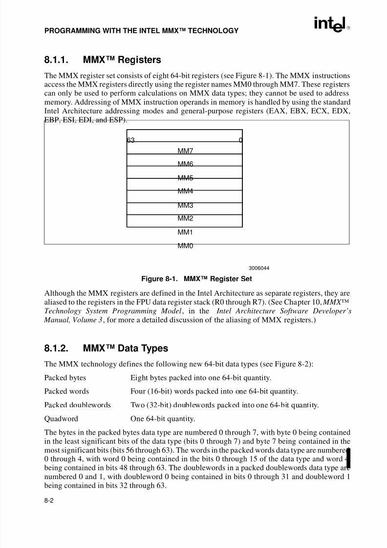
8/3/2019 Intel Architecture Software Developer's Manual, Volume 1: Basic Architecture
http://slidepdf.com/reader/full/intel-architecture-software-developers-manual-volume-1-basic-architecture 196/283
8-2
PROGRAMMING WITH THE INTEL MMX™ TECHNOLOGY
8.1.1. MMX™ Registers
The MMX register set consists of eight 64-bit registers (see Figure 8-1). The MMX instructionsaccess the MMX registers directly using the register names MM0 through MM7. These registers
can only be used to perform calculations on MMX data types; they cannot be used to addressmemory. Addressing of MMX instruction operands in memory is handled by using the standardIntel Architecture addressing modes and general-purpose registers (EAX, EBX, ECX, EDX,EBP, ESI, EDI, and ESP).
Although the MMX registers are defined in the Intel Architecture as separate registers, they arealiased to the registers in the FPU data register stack (R0 through R7). (See Chapter 10, MMX™Technology System Programming Model, in the Intel Architecture Software Developer’s
Manual, Volume 3, for more a detailed discussion of the aliasing of MMX registers.)
8.1.2. MMX™ Data Types
The MMX technology defines the following new 64-bit data types (see Figure 8-2):
Packed bytes Eight bytes packed into one 64-bit quantity.
Packed words Four (16-bit) words packed into one 64-bit quantity.
Packed doublewords Two (32-bit) doublewords packed into one 64-bit quantity.
Quadword One 64-bit quantity.
The bytes in the packed bytes data type are numbered 0 through 7, with byte 0 being containedin the least significant bits of the data type (bits 0 through 7) and byte 7 being contained in themost significant bits (bits 56 through 63). The words in the packed words data type are numbered0 through 4, with word 0 being contained in the bits 0 through 15 of the data type and word 4
being contained in bits 48 through 63. The doublewords in a packed doublewords data type arenumbered 0 and 1, with doubleword 0 being contained in bits 0 through 31 and doubleword 1being contained in bits 32 through 63.
Figure 8-1. MMX™ Register Set
63 0
MM7
MM6
MM5
MM4
MM3
MM2
MM1
MM0
3006044
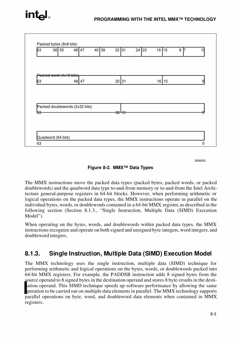
8/3/2019 Intel Architecture Software Developer's Manual, Volume 1: Basic Architecture
http://slidepdf.com/reader/full/intel-architecture-software-developers-manual-volume-1-basic-architecture 197/283
8-3
PROGRAMMING WITH THE INTEL MMX™ TECHNOLOGY
The MMX instructions move the packed data types (packed bytes, packed words, or packeddoublewords) and the quadword data type to-and-from memory or to-and-from the Intel Archi-tecture general-purpose registers in 64-bit blocks. However, when performing arithmetic orlogical operations on the packed data types, the MMX instructions operate in parallel on theindividual bytes, words, or doublewords contained in a 64-bit MMX register, as described in thefollowing section (Section 8.1.3., “Single Instruction, Multiple Data (SIMD) ExecutionModel”).
When operating on the bytes, words, and doublewords within packed data types, the MMXinstructions recognize and operate on both signed and unsigned byte integers, word integers, and
doubleword integers.
8.1.3. Single Instruction, Multiple Data (SIMD) Execution Model
The MMX technology uses the single instruction, multiple data (SIMD) technique forperforming arithmetic and logical operations on the bytes, words, or doublewords packed into64-bit MMX registers. For example, the PADDSB instruction adds 8 signed bytes from thesource operand to 8 signed bytes in the destination operand and stores 8 byte-results in the desti-nation operand. This SIMD technique speeds up software performance by allowing the sameoperation to be carried out on multiple data elements in parallel. The MMX technology supports
parallel operations on byte, word, and doubleword data elements when contained in MMXregisters.
Figure 8-2. MMX™ Data Types
3006002
63
Packed bytes (8x8 bits)
56 55 48 47 40 39 32 31 24 23 16 15 8 7 0
63
Packed word (4x16 bits)
48 47 32 31 16 15 0
63
Packed doublewords (2x32 bits)
32 31 0
63
Quadword (64 bits)
0
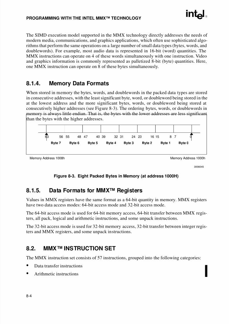
8/3/2019 Intel Architecture Software Developer's Manual, Volume 1: Basic Architecture
http://slidepdf.com/reader/full/intel-architecture-software-developers-manual-volume-1-basic-architecture 198/283
8-4
PROGRAMMING WITH THE INTEL MMX™ TECHNOLOGY
The SIMD execution model supported in the MMX technology directly addresses the needs of modern media, communications, and graphics applications, which often use sophisticated algo-rithms that perform the same operations on a large number of small data types (bytes, words, anddoublewords). For example, most audio data is represented in 16-bit (word) quantities. The
MMX instructions can operate on 4 of these words simultaneously with one instruction. Videoand graphics information is commonly represented as palletized 8-bit (byte) quantities. Here,one MMX instruction can operate on 8 of these bytes simultaneously.
8.1.4. Memory Data Formats
When stored in memory the bytes, words, and doublewords in the packed data types are storedin consecutive addresses, with the least significant byte, word, or doubleword being stored in theat the lowest address and the more significant bytes, words, or doubleword being stored atconsecutively higher addresses (see Figure 8-3). The ordering bytes, words, or doublewords inmemory is always little endian. That is, the bytes with the lower addresses are less significantthan the bytes with the higher addresses.
8.1.5. Data Formats for MMX™ Registers
Values in MMX registers have the same format as a 64-bit quantity in memory. MMX registershave two data access modes: 64-bit access mode and 32-bit access mode.
The 64-bit access mode is used for 64-bit memory access, 64-bit transfer between MMX regis-ters, all pack, logical and arithmetic instructions, and some unpack instructions.
The 32-bit access mode is used for 32-bit memory access, 32-bit transfer between integer regis-ters and MMX registers, and some unpack instructions.
8.2. MMX™ INSTRUCTION SET
The MMX instruction set consists of 57 instructions, grouped into the following categories:
• Data transfer instructions
• Arithmetic instructions
Figure 8-3. Eight Packed Bytes in Memory (at address 1000H)
3006045
63 0
Byte 7 Byte 6 Byte 5 Byte 4 Byte 3 Byte 2 Byte 1 Byte 0
56 55 48 47 40 39 32 31 24 23 16 15 8 7
Memory Address 1008h Memory Address 1000h
8/3/2019 Intel Architecture Software Developer's Manual, Volume 1: Basic Architecture
http://slidepdf.com/reader/full/intel-architecture-software-developers-manual-volume-1-basic-architecture 199/283
8-5
PROGRAMMING WITH THE INTEL MMX™ TECHNOLOGY
• Comparison instructions
• Conversion instructions
• Logical instructions
• Shift instructions
• Empty MMX™ state instruction (EMMS)
When operating on packed data within an MMX register, the data is cast by the type specifiedby the instruction. For example, the PADDB (add packed bytes) instruction treats the packeddata in an MMX register as 8 packed bytes; whereas, the PADDW (add packed words) instruc-tion treats the packed data as 4 packed words.
8.2.1. Saturation Arithmetic and Wraparound ModeThe MMX technology supports a new arithmetic capability known as saturating arithmetic.Saturation is best defined by contrasting it with wraparound mode.
In wraparound mode, results that overflow or underflow are truncated and only the lower (leastsignificant) bits of the result are returned; that is, the carry is ignored.
In saturation mode, results of an operation that overflow or underflow are clipped (saturated) toa data-range limit for the data type (see Table 8-1). The result of an operation that exceeds therange of a data-type saturates to the maximum value of the range. A result that is less than therange of a data type saturates to the minimum value of the range. This method of handling over-
flow and underflow is useful in many applications, such as color calculations.
For example, when the result exceeds the data range limit for signed bytes, it is saturated to 7FH(FFH for unsigned bytes). If a value is less than the data range limit, it is saturated to 80H forsigned bytes (00H for unsigned bytes).
Saturation provides a useful feature of avoiding wraparound artifacts. In the example of colorcalculations, saturation causes a color to remain pure black or pure white without allowing forand inversion.
MMX instructions do not indicate overflow or underflow occurrence by generating exceptionsor setting flags.
Table 8-1. Data Range Limits for Saturation
Data Type Lower Limit Upper Limit
Hexadecimal Decimal Hexadecimal Decimal
Signed Byte 80H -128 7FH 127
Signed Word 8000H -32,768 7FFFH 32,767
Unsigned Byte 00H 0 FFH 255
Unsigned Word 0000H 0 FFFFH 65,535
8/3/2019 Intel Architecture Software Developer's Manual, Volume 1: Basic Architecture
http://slidepdf.com/reader/full/intel-architecture-software-developers-manual-volume-1-basic-architecture 200/283
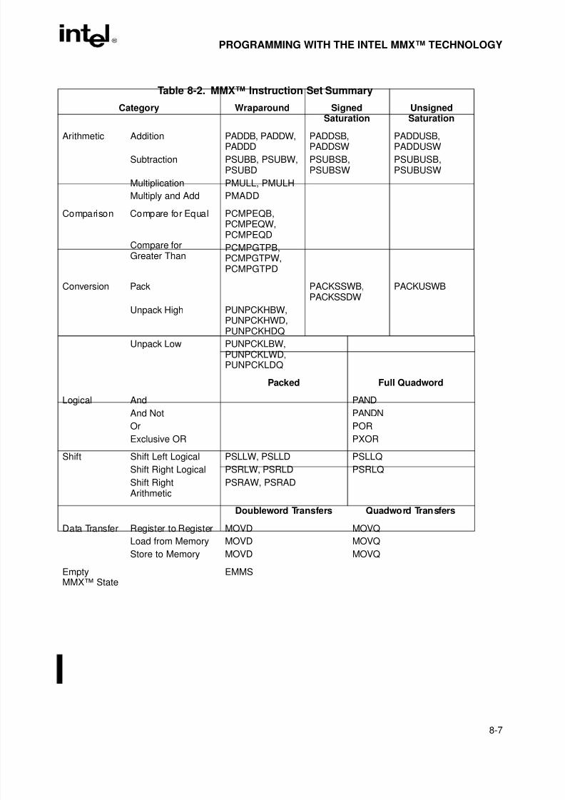
8/3/2019 Intel Architecture Software Developer's Manual, Volume 1: Basic Architecture
http://slidepdf.com/reader/full/intel-architecture-software-developers-manual-volume-1-basic-architecture 201/283
8-7
PROGRAMMING WITH THE INTEL MMX™ TECHNOLOGY
Table 8-2. MMX™ Instruction Set Summary
Category Wraparound SignedSaturation
UnsignedSaturation
Arithmetic Addition
Subtraction
Multiplication
Multiply and Add
PADDB, PADDW,PADDD
PSUBB, PSUBW,PSUBD
PMULL, PMULH
PMADD
PADDSB,PADDSW
PSUBSB,PSUBSW
PADDUSB,PADDUSW
PSUBUSB,PSUBUSW
Comparison Compare for Equal
Compare forGreater Than
PCMPEQB,PCMPEQW,PCMPEQD
PCMPGTPB,PCMPGTPW,PCMPGTPD
Conversion Pack
Unpack High
Unpack Low
PUNPCKHBW,PUNPCKHWD,PUNPCKHDQ
PUNPCKLBW,PUNPCKLWD,PUNPCKLDQ
PACKSSWB,PACKSSDW
PACKUSWB
Packed Full Quadword
Logical And
And NotOr
Exclusive OR
PAND
PANDNPOR
PXOR
Shift Shift Left Logical
Shift Right Logical
Shift RightArithmetic
PSLLW, PSLLD
PSRLW, PSRLD
PSRAW, PSRAD
PSLLQ
PSRLQ
Doubleword Transfers Quadword Transfers
Data Transfer Register to Register
Load from Memory
Store to Memory
MOVD
MOVD
MOVD
MOVQ
MOVQ
MOVQ
EmptyMMX™ State
EMMS
8/3/2019 Intel Architecture Software Developer's Manual, Volume 1: Basic Architecture
http://slidepdf.com/reader/full/intel-architecture-software-developers-manual-volume-1-basic-architecture 202/283
8-8
PROGRAMMING WITH THE INTEL MMX™ TECHNOLOGY
8.3.2. Arithmetic Instructions
The arithmetic instructions perform addition, subtraction, multiplication, and multiply/add oper-ations on packed data types.
8.3.2.1. PACKED ADDITION AND SUBTRACTION
The PADDSB, PADDSW, and PADDWD (packed add) and PSUBB, PSUBW, and PSUBD(packed subtract) instructions add or subtract the signed or unsigned data elements of the sourceoperand to or from the destination operand in wrap- around mode. These instructions supportpacked byte, packed word, and packed doubleword data types.
The PADDSB and PADDSW (packed add with saturation) and PSUBSB and PSUBSW (packedsubtract with saturation) instructions add or subtract the signed data elements of the sourceoperand to or from the signed data elements of the destination operand and saturate the result to
the limits of the signed data-type range. These instructions support packed byte and packed worddata types.
The PADDUSB and PADDUSW (packed add unsigned with saturation) and PSUBUSB andPSUBUSW (packed subtract unsigned with saturation) instructions add or subtract the unsigneddata elements of the source operand to or from the unsigned data elements of the destinationoperand and saturate the result to the limits of the unsigned data-type range. These instructionssupport packed byte and packed word data types.
8.3.2.2. PACKED MULTIPLICATION
Packed multiplication instructions perform four multiplications on pairs of signed 16-bit oper-ands, producing 32-bit intermediate results. Users may choose the low-order or high-order partsof each 32-bit result.
The PMULHW (packed multiply high) and PMULLW (packed multiply low) instructionsmultiply the signed words of the source and destination operands and write the high-order orlow-order 16 bits of each of the results to the destination operand.
8.3.2.3. PACKED MULTIPLY ADD
The PMADDWD (packed multiply and add) instruction calculates the products of the signedwords of the source and destination operands. The four intermediate 32-bit doubleword productsare summed in pairs to produce two 32-bit doubleword results.
8.3.3. Comparison Instructions
The PCMPEQB, PCMPEQW, and PCMPEQD (packed compare for equal) and PCMPGTB,PCMPGTW, and PCMPGTD (packed compare for greater than) instructions compare the corre-sponding data elements in the source and destination operands for equality or value greater than,respectively. These instructions generate a mask of ones or zeros which are written to the desti-
nation operand. Logical operations can use the mask to select elements. This can be used to
8/3/2019 Intel Architecture Software Developer's Manual, Volume 1: Basic Architecture
http://slidepdf.com/reader/full/intel-architecture-software-developers-manual-volume-1-basic-architecture 203/283
8-9
PROGRAMMING WITH THE INTEL MMX™ TECHNOLOGY
implement a packed conditional move operation without a branch or a set of branch instructions.No flags are set.
These instructions support packed byte, packed word and packed doubleword data types.
8.3.4. Conversion Instructions
The conversion instructions convert the data elements within a packed data type.
The PACKSSWB and PACKSSDW (packed with signed saturation) instruction converts signedwords into signed bytes or signed doublewords into signed words, in signed saturation mode.
The PACKUSWB (packed with unsigned saturation) instruction converts signed words intounsigned bytes, in unsigned saturation mode.
The PUNPCKHBW, PUNPCKHWD, and PUNPCKHDQ (unpack high packed data) andPUNPCKLBW, PUNPCKLWD, and PUNPCKLDQ (unpack low packed data) instructionsconvert bytes to words, words to doublewords, or doublewords to quadwords.
8.3.5. Logical Instructions
The PAND (bitwise logical AND), PANDN (bitwise logical AND NOT), POR (bitwise logicalOR), and PXOR (bitwise logical exclusive OR) instructions perform bitwise logical operationson 64-bit quantities.
8.3.6. Shift Instructions
The logical shift left, logical shift right and arithmetic shift right instructions shift each elementby a specified number of bits. The logical left and right shifts also enable a 64-bit quantity (quad-word) to be shifted as one block, assisting in data type conversions and alignment operations.
The PSLLW and PSLLD (packed shift left logical) and PSRLW and PSRLD (packed shift rightlogical) instructions perform a logical left or right shift, and fill the empty high or low order bitpositions with zeros. These instructions support packed word, packed doubleword, and quad-word data types.
The PSRAW and PSRAD (packed shift right arithmetic) instruction performs an arithmetic rightshift, copying the sign bit into empty bit positions on the upper end of the operand. This instruc-tion supports packed word and packed doubleword data types.
8.3.7. EMMS (Empty MMX™ State) Instruction
The EMMS instruction empties the MMX state. This instruction must be used to clear the MMXstate (empty the floating-point tag word) at the end of an MMX routine before calling otherroutines that can execute floating-point instructions.
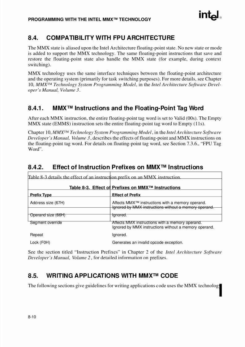
8/3/2019 Intel Architecture Software Developer's Manual, Volume 1: Basic Architecture
http://slidepdf.com/reader/full/intel-architecture-software-developers-manual-volume-1-basic-architecture 204/283
8-10
PROGRAMMING WITH THE INTEL MMX™ TECHNOLOGY
8.4. COMPATIBILITY WITH FPU ARCHITECTURE
The MMX state is aliased upon the Intel Architecture floating-point state. No new state or modeis added to support the MMX technology. The same floating-point instructions that save and
restore the floating-point state also handle the MMX state (for example, during contextswitching).
MMX technology uses the same interface techniques between the floating-point architectureand the operating system (primarily for task switching purposes). For more details, see Chapter10, MMX™ Technology System Programming Model, in the Intel Architecture Software Devel-oper’s Manual, Volume 3.
8.4.1. MMX™ Instructions and the Floating-Point Tag Word
After each MMX instruction, the entire floating-point tag word is set to Valid (00s). The EmptyMMX state (EMMS) instruction sets the entire floating-point tag word to Empty (11s).
Chapter 10, MMX™ Technology System Programming Model, in the Intel Architecture Software
Developer’s Manual, Volume 3, describes the effects of floating-point and MMX instructions onthe floating-point tag word. For details on floating-point tag word, see Section 7.3.6., “FPU TagWord”.
8.4.2. Effect of Instruction Prefixes on MMX™ Instructions
Table 8-3 details the effect of an instruction prefix on an MMX instruction.
See the section titled “Instruction Prefixes” in Chapter 2 of the Intel Architecture Software Developer’s Manual, Volume 2 , for detailed information on prefixes.
8.5. WRITING APPLICATIONS WITH MMX™ CODE
The following sections give guidelines for writing applications code uses the MMX technology.
Table 8-3. Effect of Prefixes on MMX™ Instructions
Prefix Type Effect of Prefix
Address size (67H) Affects MMX™ instructions with a memory operand.Ignored by MMX instructions without a memory operand.
Operand size (66H) Ignored.
Segment override Affects MMX instructions with a memory operand.Ignored by MMX instructions without a memory operand.
Repeat Ignored.
Lock (F0H) Generates an invalid opcode exception.
8/3/2019 Intel Architecture Software Developer's Manual, Volume 1: Basic Architecture
http://slidepdf.com/reader/full/intel-architecture-software-developers-manual-volume-1-basic-architecture 205/283
8-11
PROGRAMMING WITH THE INTEL MMX™ TECHNOLOGY
8.5.1. Detecting Support for MMX™ Technology Using theCPUID Instruction
Use the CPUID instruction to determine whether the processor supports the MMX instruction
set (see the section titled “CPUID—CPU Identification” in Chapter 3 of the Intel ArchitectureSoftware Developer’s Manual, Volume 2, for a detailed description of the CPUID instruction).When the support for MMX technology is detected by the CPUID instruction, it is signaled bysetting bit 23 (MMX technology bit) in the feature flags to 1. In general, two versions of theroutine can be created: one with scalar instructions and one with MMX instructions. The appli-cation will call the appropriate routine depending on the results of the CPUID instruction. If support for MMX technology is detected, then the MMX routine is called; if no support for theMMX technology exists, the application calls the scalar routine.
NOTE
The CPUID instruction will continue to report the existence of the MMXtechnology if the CR0.EM bit is set (which signifies that the CPU isconfigured to generate exception interrupt 7 that can be used to emulatefloating point instructions). In this case, executing an MMX instructionresults in an invalid opcode exception.
Example 8-1 illustrates how to use the CPUID instruction. This example does not represent theentire CPUID sequence, but shows the portion used for detection of MMX technology.
Example 8-1. Partial Routine for Detecting MMX™ Technology with the CPUID Instruction
... ; identify existence of CPUID instruction
...
... ; identify Intel processor
....
mov EAX, 1 ; request for feature flags
CPUID ; 0Fh, 0A2h CPUID instruction
test EDX, 00800000h ; Is IA MMX technology bit (Bit 23 of EDX)
; in feature flags set?
jnz MMX_Technology_Found
8.5.2. Using the EMMS Instruction
When integrating an MMX routine into an application running under an existing operatingsystem, programmers need to take special precautions, similar to those when writing floating-point code.
When an MMX instruction executes, the floating-point tag word is marked valid (00s). Subse-quent floating-point instructions that will be executed may produce unexpected results becausethe floating-point stack seems to contain valid data. The EMMS instruction marks the floating-
8/3/2019 Intel Architecture Software Developer's Manual, Volume 1: Basic Architecture
http://slidepdf.com/reader/full/intel-architecture-software-developers-manual-volume-1-basic-architecture 206/283
8-12
PROGRAMMING WITH THE INTEL MMX™ TECHNOLOGY
point tag word as empty. Therefore, it is imperative to use the EMMS instruction at the end of every MMX routine, if the next routine may contain FPU code.
The EMMS instruction must be used in each of the following cases:
• When an application using the floating-point instructions calls an MMX™ technologylibrary/DLL. (Use the EMMS instruction at the end of the MMX code.)
• When an application using MMX instructions calls a floating-point library/DLL. (Use theEMMS instruction before calling the floating-point code.)
• When a switch is made between MMX code in a task/thread and other tasks/threads incooperative operating systems, unless it is certain that more MMX instructions will beexecuted before any FPU code.
If the EMMS instruction is not used when trying to execute a floating-point instruction, thefollowing may occur:
• Depending on the exception mask bits of the floating-point control word, a floating- pointexception event may be generated.
• A “soft exception” may occur. In this case floating-point code continues to execute, butgenerates incorrect results. This happens when the floating-point exceptions are maskedand no visible exceptions occur. The internal exception handler (microcode, not uservisible) loads a NaN (Not a Number) with an exponent of 11..11B onto the floating-pointstack. The NaN is used for further calculations, yielding incorrect results.
• A potential error may occur only if the operating system does NOT manage floating-pointcontext across task switches. These operating systems are usually cooperative operating
systems. It is imperative that the EMMS instruction execute at the end of all the MMX™routines that may enable a task switch immediately after they end execution (explicit yieldAPI or implicit yield API).
8.5.3. Interfacing with MMX™ Code
The MMX technology enables direct access to all the MMX registers. This means that allexisting interface conventions that apply to the use of the processor’s general-purpose registers(EAX, EBX, etc.) also apply to use of MMX register.
An efficient interface to MMX routines might pass parameters and return values through theMMX registers or through a combination of memory locations (via the stack) and MMX regis-ters. Such an interface would have to be written in assembly language since passing parametersthrough MMX registers is not currently supported by any existing C compilers. Do not use theEMMS instruction when the interface to the MMX code has been defined to retain values in theMMX register.
If a high-level language, such as C, is used, the data types could be defined as a 64-bit structurewith packed data types.
When implementing usage of MMX instructions in high-level languages other approaches can
be taken, such as:
8/3/2019 Intel Architecture Software Developer's Manual, Volume 1: Basic Architecture
http://slidepdf.com/reader/full/intel-architecture-software-developers-manual-volume-1-basic-architecture 207/283
8-13
PROGRAMMING WITH THE INTEL MMX™ TECHNOLOGY
• Passing parameters to an MMX™ routine by passing a pointer to a structure via the integerstack.
• Returning a value from a function by returning the pointer to a structure.
8.5.4. Writing Code with MMX™ and Floating-Point Instructions
The MMX technology aliases the MMX registers on the floating-point registers. The mainreason for this is to enable MMX technology to be fully compatible and transparent to existingsoftware environments (operating systems and applications). This way operating systems willbe able to include new applications and drivers that use the MMX technology.
An application can contain both floating-point and MMX code. However, the user is discour-aged from causing frequent transitions between MMX and floating-point instructions by mixing
MMX code and floating-point code.
8.5.4.1. RECOMMENDATIONS AND GUIDELINES
Do not mix MMX code and floating-point code at the instruction level for the following reasons:
• The TOS (top of stack) value of the floating-point status word is set to 0 after eachMMX™ instruction. This means that the floating-point code loses its pointer to itsfloating-point registers if the code mixes MMX instructions within a floating-point routine.
• An MMX instruction write to an MMX register writes ones (11s) to the exponent part of the corresponding floating-point register.
• Floating-point code that uses register contents that were generated by the MMX instruc-tions may cause floating-point exceptions or incorrect results. These floating-pointexceptions are related to undefined floating-point values and floating-point stack usage.
• All MMX instructions (except EMMS) set the entire tag word to the valid state (00s in alltag fields) without preserving the previous floating-point state.
• Frequent transitions between the MMX and floating-point instructions may result insignificant performance degradation in some implementations.
If the application contains floating-point and MMX instructions, follow these guidelines:
• Partition the MMX™ technology module and the floating-point module into separateinstruction streams (separate loops or subroutines) so that they contain only instructions of one type.
• Do not rely on register contents across transitions.
• When the MMX state is not required, empty the MMX state using the EMMS instruction.
• Exit the floating-point code section with an empty stack.
8/3/2019 Intel Architecture Software Developer's Manual, Volume 1: Basic Architecture
http://slidepdf.com/reader/full/intel-architecture-software-developers-manual-volume-1-basic-architecture 208/283
8-14
PROGRAMMING WITH THE INTEL MMX™ TECHNOLOGY
Example 8-2. Floating-point (FP) and MMX™ Code
FP_code:
..
.. (*leave the FPU stack empty*)MMX_code:
..
EMMS (*mark the FPU tag word as empty*)
FP_code 1:
..
.. (*leave the FPU stack empty*)
8.5.5. Using MMX™ Code in a Multitasking Operating SystemEnvironment
An application needs to identify the nature of the multitasking operating system on which itruns. Each task retains its own state which must be saved when a task switch occurs. Theprocessor state (context) consists of the general-purpose registers and the floating-point andMMX registers.
Operating systems can be classified into two types:
• Cooperative multitasking operating system.
• Preemptive multitasking operating system.
The behavior of the two operating-system types in context switching is described in “ContextSwitching” in Chapter 10 of the Intel Architecture Software Developer’s Manual, Volume 3.
8.5.5.1. COOPERATIVE MULTITASKING OPERATING SYSTEM
Cooperative multitasking operating systems do not save the FPU or MMX state whenperforming a context switch. Therefore, the application needs to save the relevant state beforerelinquishing direct or indirect control to the operating system.
8.5.5.2. PREEMPTIVE MULTITASKING OPERATING SYSTEM
Preemptive multitasking operating systems are responsible for saving and restoring the FPU andMMX state when performing a context switch. Therefore, the application does not have to saveor restore the FPU and MMX state.
8/3/2019 Intel Architecture Software Developer's Manual, Volume 1: Basic Architecture
http://slidepdf.com/reader/full/intel-architecture-software-developers-manual-volume-1-basic-architecture 209/283
8-15
PROGRAMMING WITH THE INTEL MMX™ TECHNOLOGY
8.5.6. Exception Handling in MMX™ Code
MMX instructions generate the same type of memory-access exceptions as other Intel Architec-ture instructions. Some examples are: page fault, segment not present, and limit violations.
Existing exception handlers can handle these types of exceptions. They do not have to be modi-fied.
Unless there is a pending floating-point exception, MMX instructions do not generate numericexceptions. Therefore, there is no need to modify existing exception handlers or add new ones.
If a floating-point exception is pending, the subsequent MMX instruction generates a numericerror exception (interrupt 16 and/or FERR#). The MMX instruction resumes execution uponreturn from the exception handler.
8.5.7. Register MappingThe MMX registers and their tags are mapped to physical locations of the floating-point regis-ters and their tags. Register aliasing and mapping is described in more detail in Chapter 10,
MMX™ Technology System Programming Model , in the Intel Architecture Software Developer’s Manual, Volume 3.

8/3/2019 Intel Architecture Software Developer's Manual, Volume 1: Basic Architecture
http://slidepdf.com/reader/full/intel-architecture-software-developers-manual-volume-1-basic-architecture 210/283
8/3/2019 Intel Architecture Software Developer's Manual, Volume 1: Basic Architecture
http://slidepdf.com/reader/full/intel-architecture-software-developers-manual-volume-1-basic-architecture 211/283
9Input/Output

8/3/2019 Intel Architecture Software Developer's Manual, Volume 1: Basic Architecture
http://slidepdf.com/reader/full/intel-architecture-software-developers-manual-volume-1-basic-architecture 212/283
8/3/2019 Intel Architecture Software Developer's Manual, Volume 1: Basic Architecture
http://slidepdf.com/reader/full/intel-architecture-software-developers-manual-volume-1-basic-architecture 213/283
9-1
CHAPTER 9INPUT/OUTPUT
In addition to transferring data to and from external memory, Intel Architecture processors canalso transfer data to and from input/output ports (I/O ports). I/O ports are created in system hard-ware by circuity that decodes the control, data, and address pins on the processor. These I/Oports are then configured to communicate with peripheral devices. An I/O port can be an inputport, an output port, or a bidirectional port. Some I/O ports are used for transmitting data, suchas to and from the transmit and receive registers, respectively, of a serial interface device. OtherI/O ports are used to control peripheral devices, such as the control registers of a disk controller.
This chapter describes the processor’s I/O architecture. The topics discussed include:
• I/O port addressing.
• I/O instructions.
• I/O protection mechanism.
9.1. I/O PORT ADDRESSING
The processor allows I/O ports to be accessed in either of two ways:
• Through a separate I/O address space.
• Through memory-mapped I/O.
Accessing I/O ports through the I/O address space is handled through a set of I/O instructionsand a special I/O protection mechanism. Accessing I/O ports through memory-mapped I/O ishandled with the processors general-purpose move and string instructions, with protectionprovided through segmentation or paging. I/O ports can be mapped so that they appear in the I/Oaddress space or the physical-memory address space (memory mapped I/O) or both.
One benefit of using the I/O address space is that writes to I/O ports are guaranteed to becompleted before the next instruction in the instruction stream is executed. Thus, I/O writes tocontrol system hardware cause the hardware to be set to its new state before any other instruc-
tions are executed. See Section 9.6., “Ordering I/O”, for more information on serializing of I/Ooperations.
9.2. I/O PORT HARDWARE
From a hardware point of view, I/O addressing is handled through the processor’s address lines.For Pentium Pro processors, a special memory-I/O transaction on the system bus indicateswhether the address lines are being driven with a memory address or an I/O address; for Pentiumand earlier Intel Architecture processors, the M/IO pin indicates a memory address (1) or an I/Oaddress (0). When the separate I/O address space is selected, it is the responsibility of the hard-
ware to decode the memory-I/O bus transaction to select I/O ports rather than memory.Data is transmitted between the processor and an I/O device through the data lines.
8/3/2019 Intel Architecture Software Developer's Manual, Volume 1: Basic Architecture
http://slidepdf.com/reader/full/intel-architecture-software-developers-manual-volume-1-basic-architecture 214/283
9-2
INPUT/OUTPUT
9.3. I/O ADDRESS SPACE
The processor’s I/O address space is separate and distinct from the physical-memory addressspace. The I/O address space consists of 216 (64K) individually addressable 8-bit I/O ports,
numbered 0 through FFFFH. I/O port addresses 0F8H through 0FFH are reserved. Do not assignI/O ports to these addresses. The result of an attempt to address beyond the I/O address spacelimit of FFFFH is implementation-specific; see the Developer’s Manuals for specific processorsfor more details.
Any two consecutive 8-bit ports can be treated as a 16-bit port, and any four consecutive portscan be a 32-bit port. In this manner, the processor can transfer 8, 16, or 32 bits to or from a devicein the I/O address space. Like words in memory, 16-bit ports should be aligned to even addresses(0, 2, 4, ...) so that all 16 bits can be transferred in a single bus cycle. Likewise, 32-bit portsshould be aligned to addresses that are multiples of four (0, 4, 8, ...). The processor supports datatransfers to unaligned ports, but there is a performance penalty because one or more extra bus
cycle must be used.
The exact order of bus cycles used to access unaligned ports is undefined and is not guaranteedto remain the same in future Intel Architecture processors. If hardware or software requires thatI/O ports be written to in a particular order, that order must be specified explicitly. For example,to load a word-length I/O port at address 2H and then another word port at 4H, two word-lengthwrites must be used, rather than a single doubleword write at 2H.
Note that the processor does not mask parity errors for bus cycles to the I/O address space.Accessing I/O ports through the I/O address space is thus a possible source of parity errors.
9.3.1. Memory-Mapped I/O
I/O devices that respond like memory components can be accessed through the processor’s phys-ical-memory address space (see Figure 9-1). When using memory-mapped I/O, any of theprocessor’s instructions that reference memory can be used to access an I/O port located at aphysical-memory address. For example, the MOV instruction can transfer data between anyregister and a memory-mapped I/O port. The AND, OR, and TEST instructions may be used tomanipulate bits in the control and status registers of a memory-mapped peripheral devices.
When using memory-mapped I/O, caching of the address space mapped for I/O operations mustbe prevented. With the Pentium Pro processors, caching of I/O accesses can be prevented by
using memory type range registers (MTRRs) to map the address space used for the memory-mapped I/O as uncacheable (UC). See Chapter 9, Memory Cache Control, in the Intel Architec-
ture Software Developer’s Manual, Volume 3, for a complete discussion of the MTRRs.
The Pentium and Intel486 processors do not support MTRRs. Instead, they provide the KEN#pin, which when held inactive (high) prevents caching of all addresses sent out on the systembus. To use this pin, external address decoding logic is required to block caching in specificaddress spaces.
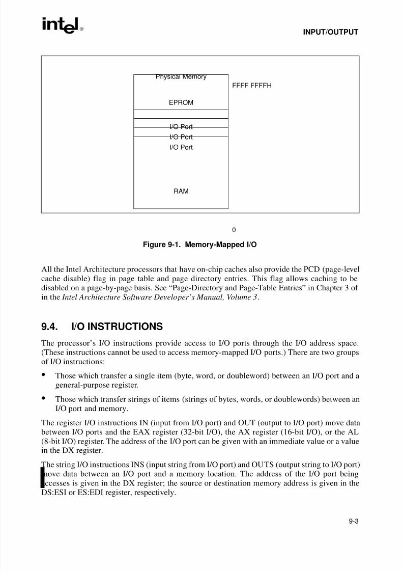
8/3/2019 Intel Architecture Software Developer's Manual, Volume 1: Basic Architecture
http://slidepdf.com/reader/full/intel-architecture-software-developers-manual-volume-1-basic-architecture 215/283
8/3/2019 Intel Architecture Software Developer's Manual, Volume 1: Basic Architecture
http://slidepdf.com/reader/full/intel-architecture-software-developers-manual-volume-1-basic-architecture 216/283
9-4
INPUT/OUTPUT
When used with one of the repeat prefixes (such as REP), the INS and OUTS instructionsperform string (or block) input or output operations. The repeat prefix REP modifies the INS andOUTS instructions to transfer blocks of data between an I/O port and memory. Here, the ESI orEDI register is incremented or decremented (according to the setting of the DF flag in the
EFLAGS register) after each byte, word, or doubleword is transferred between the selected I/Oport and memory.
See the individual references for the IN, INS, OUT, and OUTS instructions in Chapter 3, Instruction Set Reference, of the Intel Architecture Software Developer’s Manual, Volume 2, formore information on these instructions.
9.5. PROTECTED-MODE I/O
When the processor is running in protected mode, the following protection mechanisms regulate
access to I/O ports:
• When accessing I/O ports through the I/O address space, two protection devices controlaccess:
— The I/O privilege level (IOPL) field in the EFLAGS register.
— The I/O permission bit map of a task state segment (TSS).
• When accessing memory-mapped I/O ports, the normal segmentation and pagingprotection and the MTRRs (in processors that support them) also affect access to I/O ports.See Chapter 4, Protection, and Chapter 9, Memory Cache Control, in the Intel Architecture
Software Developer’s Manual, Volume 3 , for a complete discussion of memory protection.The following sections describe the protection mechanisms available when accessing I/O portsin the I/O address space with the I/O instructions.
9.5.1. I/O Privilege Level
In systems where I/O protection is used, the IOPL field in the EFLAGS register controls accessto the I/O address space by restricting use of selected instructions. This protection mechanismpermits the operating system or executive to set the privilege level needed to perform I/O. In atypical protection ring model, access to the I/O address space is restricted to privilege levels 0and 1. Here, kernel and the device drivers are allowed to perform I/O, while less privilegeddevice drivers and application programs are denied access to the I/O address space. Applicationprograms must then make calls to the operating system to perform I/O.
The following instructions can be executed only if the current privilege level (CPL) of theprogram or task currently executing is less than or equal to the IOPL: IN, INS, OUT, OUTS, CLI(clear interrupt-enable flag), and STI (set interrupt-enable flag). These instructions are called
I/O sensitive instructions, because they are sensitive to the IOPL field. Any attempt by a lessprivileged program or task to use an I/O sensitive instruction results in a general-protectionexception (#GP) being signaled. Because each task has its own copy of the EFLAGS register,each task can have a different IOPL.
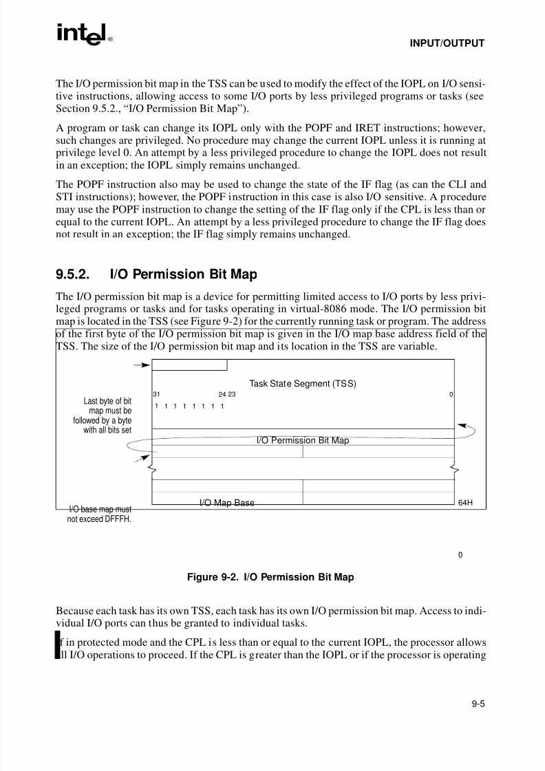
8/3/2019 Intel Architecture Software Developer's Manual, Volume 1: Basic Architecture
http://slidepdf.com/reader/full/intel-architecture-software-developers-manual-volume-1-basic-architecture 217/283
9-5
INPUT/OUTPUT
The I/O permission bit map in the TSS can be used to modify the effect of the IOPL on I/O sensi-tive instructions, allowing access to some I/O ports by less privileged programs or tasks (seeSection 9.5.2., “I/O Permission Bit Map”).
A program or task can change its IOPL only with the POPF and IRET instructions; however,such changes are privileged. No procedure may change the current IOPL unless it is running atprivilege level 0. An attempt by a less privileged procedure to change the IOPL does not resultin an exception; the IOPL simply remains unchanged.
The POPF instruction also may be used to change the state of the IF flag (as can the CLI andSTI instructions); however, the POPF instruction in this case is also I/O sensitive. A proceduremay use the POPF instruction to change the setting of the IF flag only if the CPL is less than orequal to the current IOPL. An attempt by a less privileged procedure to change the IF flag doesnot result in an exception; the IF flag simply remains unchanged.
9.5.2. I/O Permission Bit Map
The I/O permission bit map is a device for permitting limited access to I/O ports by less privi-leged programs or tasks and for tasks operating in virtual-8086 mode. The I/O permission bitmap is located in the TSS (see Figure 9-2) for the currently running task or program. The addressof the first byte of the I/O permission bit map is given in the I/O map base address field of theTSS. The size of the I/O permission bit map and its location in the TSS are variable.
Because each task has its own TSS, each task has its own I/O permission bit map. Access to indi-vidual I/O ports can thus be granted to individual tasks.
If in protected mode and the CPL is less than or equal to the current IOPL, the processor allowsall I/O operations to proceed. If the CPL is greater than the IOPL or if the processor is operating
Figure 9-2. I/O Permission Bit Map
I/O Map Base
Task State Segment (TSS)
64H
31 24 23 01 1111111
I/O Permission Bit Map
0
I/O base map mustnot exceed DFFFH.
Last byte of bitmap must be
followed by a bytewith all bits set
8/3/2019 Intel Architecture Software Developer's Manual, Volume 1: Basic Architecture
http://slidepdf.com/reader/full/intel-architecture-software-developers-manual-volume-1-basic-architecture 218/283
9-6
INPUT/OUTPUT
in virtual-8086 mode, the processor checks the I/O permission bit map to determine if access toa particular I/O port is allowed. Each bit in the map corresponds to an I/O port byte address. Forexample, the control bit for I/O port address 29H in the I/O address space is found at bit position1 of the sixth byte in the bit map. Before granting I/O access, the processor tests all the bits corre-
sponding to the I/O port being addressed. For a doubleword access, for example, the processorstests the four bits corresponding to the four adjacent 8-bit port addresses. If any tested bit is set,a general-protection exception (#GP) is signaled. If all tested bits are clear, the I/O operation isallows to proceed.
Because I/O port addresses are not necessarily aligned to word and doubleword boundaries, theprocessor read two bytes from the I/O permission bit map for every access to an I/O port. Toprevent exceptions from being generated when the ports with the highest addresses are accessed,an extra byte needs to included in the TSS immediately after the table. This byte must have allof its bits set, and it must be within the segment limit.
It is not necessary for the I/O permission bit map to represent all the I/O addresses. I/O addressesnot spanned by the map are treated as if they had set bits in the map. For example, if the TSSsegment limit is 10 bytes past the bit-map base address, the map has 11 bytes and the first 80 I/Oports are mapped. Higher addresses in the I/O address space generate exceptions.
If the I/O bit map base address is greater than or equal to the TSS segment limit, there is no I/Opermission map, and all I/O instructions generate exceptions when the CPL is greater than thecurrent IOPL. The I/O bit map base address must be less than or equal to DFFFH.
9.6. ORDERING I/O
When controlling I/O devices it is often important that memory and I/O operations be carriedout in precisely the order programmed. For example, a program may write a command to an I/Oport, then read the status of the I/O device from another I/O port. It is important that the statusreturned be the status of the device after it receives the command, not before.
When using memory-mapped I/O, caution should be taken to avoid situations in which theprogrammed order is not preserved by the processor. To optimize performance, the processorallows cacheable memory reads to be reordered ahead of buffered writes in most situations.Internally, processor reads (cache hits) can be reordered around buffered writes. When usingmemory-mapped I/O, therefore, is possible that an I/O read might be performed before thememory write of a previous instruction. The recommended method of enforcing programordering of memory-mapped I/O accesses with the Pentium Pro processor is to use the MTRRsto make the memory mapped I/O address space uncacheable; for the Pentium and Intel486processors, either the #KEN pin or the PCD flags can be used for this purpose (see Section9.3.1., “Memory-Mapped I/O”). When the target of a read or write is in an uncacheable regionof memory, memory reordering does not occur externally at the processor’s pins (that is, readsand writes appear in-order). Designating a memory mapped I/O region of the address space asuncacheable insures that reads and writes of I/O devices are carried out in program order. SeeChapter 9, Memory Cache Control, in the Intel Architecture Software Developer’s Manual,Volume 3, for more information on using MTRRs.
8/3/2019 Intel Architecture Software Developer's Manual, Volume 1: Basic Architecture
http://slidepdf.com/reader/full/intel-architecture-software-developers-manual-volume-1-basic-architecture 219/283
9-7
INPUT/OUTPUT
Another method of enforcing program order is to insert one of the serializing instructions, suchas the CPUID instruction, between operations. See Chapter 7, Multiple Processor Management ,in the Intel Architecture Software Developer’s Manual, Volume 3 , for more information on seri-alization of instructions.
It should be noted that the chip set being used to support the processor (bus controller, memorycontroller, and/or I/O controller) may post writes to uncacheable memory which can lead to out-of-order execution of memory accesses. In situations where out-of-order processing of memoryaccesses by the chip set can potentially cause faulty memory-mapped I/O processing, code mustbe written to force synchronization and ordering of I/O operations. Serializing instructions canoften be used for this purpose.
When the I/O address space is used instead of memory-mapped I/O, the situation is different intwo respects:
• The processor never buffers I/O writes. Therefore, strict ordering of I/O operations is
enforced by the processor. (As with memory-mapped I/O, it is possible for a chip set topost writes in certain I/O ranges.)
• The processor synchronizes I/O instruction execution with external bus activity (see Table9-1).
Table 9-1. I/O Instruction Serialization
Instruction BeingExecuted
Processor Delays Execution of … Until Completion of …
CurrentInstruction? Next Instruction? Pending Stores? Current Store?
IN Yes Yes
INS Yes Yes
REP INS Yes Yes
OUT Yes Yes Yes
OUTS Yes Yes Yes
REP OUTS Yes Yes Yes

8/3/2019 Intel Architecture Software Developer's Manual, Volume 1: Basic Architecture
http://slidepdf.com/reader/full/intel-architecture-software-developers-manual-volume-1-basic-architecture 220/283
8/3/2019 Intel Architecture Software Developer's Manual, Volume 1: Basic Architecture
http://slidepdf.com/reader/full/intel-architecture-software-developers-manual-volume-1-basic-architecture 221/283
10ProcessorIdentification
and FeatureDetermination

8/3/2019 Intel Architecture Software Developer's Manual, Volume 1: Basic Architecture
http://slidepdf.com/reader/full/intel-architecture-software-developers-manual-volume-1-basic-architecture 222/283
8/3/2019 Intel Architecture Software Developer's Manual, Volume 1: Basic Architecture
http://slidepdf.com/reader/full/intel-architecture-software-developers-manual-volume-1-basic-architecture 223/283
10-1
CHAPTER 10PROCESSOR IDENTIFICATION AND FEATURE
DETERMINATION
When writing software intended to run on several different types of Intel Architecture proces-sors, it is generally necessary to identify the type of processor present in a system and theprocessor features that are available to an application. This chapter describes how to identify theprocessor that is executing the code and determine the features the processor supports. It alsoshows how to determine if an FPU or NPX is present. See Chapter 17, Intel ArchitectureCompatibility, in the Intel Architecture Software Developer’s Manual, Volume 3, for a completelist of the features that are available for the different Intel Architecture processors.
10.1. PROCESSOR IDENTIFICATION
The CPUID instruction returns the processor type for the processor that executes the instruction.It also indicates the features that are present in the processor, including the existence of anon-chip FPU. The following information can be obtained with this instruction:
• The highest operand value the instruction responds to (2 for the Pentium® Pro processorsand 1 for the Pentium processors and recent Intel486™ processors).
• The processor’s family identification (ID) number, model ID, and stepping ID.
• The presence of an on-chip FPU.
• Support for or the presence of the following architectural extensions and enhancements:
— Virtual-8086 mode enhancements.
— Debugging extensions.
— Page-size extensions.
— Read time stamp counter (RDTSC) instruction.
— Read model specific registers (RDMSR) and write model specific registers (WRMSR)instructions.
— Physical address extension.
— Machine check exceptions.
— Compare and exchange 8 bytes instruction (CMPXCHG8B).
— On-chip, advanced programmable interrupt controller (APIC).
— Memory-type range registers (MTRRs).
— Page global flag.
8/3/2019 Intel Architecture Software Developer's Manual, Volume 1: Basic Architecture
http://slidepdf.com/reader/full/intel-architecture-software-developers-manual-volume-1-basic-architecture 224/283
8/3/2019 Intel Architecture Software Developer's Manual, Volume 1: Basic Architecture
http://slidepdf.com/reader/full/intel-architecture-software-developers-manual-volume-1-basic-architecture 225/283
10-3
PROCESSOR IDENTIFICATION AND FEATURE DETERMINATION
10.2. IDENTIFICATION OF EARLIER INTEL ARCHITECTUREPROCESSORS
The CPUID instruction is only available in the Pentium Pro, Pentium, and recent Intel486
processors. For the earlier Intel Architecture processors (including the earlier Intel486 proces-sors), several other architectural features can be exploited to identify the processor.
The settings of bits 12 and 13 (IOPL), 14 (NT), and 15 (reserved) in the EFLAGS register (seeFigure 3-7) is different for Intel’s 32-bit processors than for the Intel 8086 and Intel 286 proces-sors. By examining the settings of these bits (with the PUSHF/PUSHFD and POP/POPFDinstructions), an application program can determine whether the processor is an 8086, Intel286,or one of the Intel 32-bit processors:
• 8086 processor — Bits 12 through 15 of the EFLAGS register are always set.
• Intel 286 processor — Bits 12 through 15 are always clear in real-address mode.
• 32-bit processors — In real-address mode, bit 15 is always clear and bits 12 through 14have the last value loaded into them. In protected mode, bit 15 is always clear, bit 14 hasthe last value loaded into it, and the IOPL bits depends on the current privilege level (CPL).The IOPL field can be changed only if the CPL is 0.
Other EFLAG register bits that can be used to differentiate between the 32-bit processors:
• Bit 18 (AC) — Implemented only on the Pentium® Pro, Pentium, and Intel486™processors. The inability to set or clear this bit distinguishes an Intel386 processor from theother Intel 32-bit processors.
• Bit 21 (ID) — Determines if the processor is able to execute the CPUID instruction. Theability to set and clear this bit indicates that the processor is a Pentium Pro, Pentium, orlater version Intel486 processor.
To determine whether an FPU or NPX is present in a system, applications can write to theFPU/NPX status and control registers using the FNINIT instruction and then verify the correctvalues are read back using the FNSTENV instruction.
After determining that an FPU or NPX is present, its type can then be determined. In most cases,the processor type will determine the type of FPU or NPX; however, an Intel386 processor iscompatible with either an Intel 287 or Intel 387 math coprocessor. The method the coprocessoruses to represent ∞ (after the execution of the FINIT, FNINIT, or RESET instruction) indicates
which coprocessor is present. The Intel 287 math coprocessor uses the same bit representationfor +∞ and −∞; whereas, the Intel 387 math coprocessor uses different representations for +∞and −∞.

8/3/2019 Intel Architecture Software Developer's Manual, Volume 1: Basic Architecture
http://slidepdf.com/reader/full/intel-architecture-software-developers-manual-volume-1-basic-architecture 226/283
8/3/2019 Intel Architecture Software Developer's Manual, Volume 1: Basic Architecture
http://slidepdf.com/reader/full/intel-architecture-software-developers-manual-volume-1-basic-architecture 227/283
AEFLAGSCross-Reference

8/3/2019 Intel Architecture Software Developer's Manual, Volume 1: Basic Architecture
http://slidepdf.com/reader/full/intel-architecture-software-developers-manual-volume-1-basic-architecture 228/283
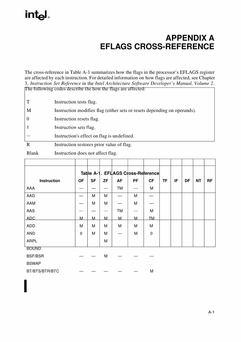
8/3/2019 Intel Architecture Software Developer's Manual, Volume 1: Basic Architecture
http://slidepdf.com/reader/full/intel-architecture-software-developers-manual-volume-1-basic-architecture 229/283
A-1
APPENDIX AEFLAGS CROSS-REFERENCE
The cross-reference in Table A-1 summarizes how the flags in the processor’s EFLAGS registerare affected by each instruction. For detailed information on how flags are affected, see Chapter3, Instruction Set Reference in the Intel Architecture Software Developer’s Manual, Volume 2.The following codes describe the how the flags are affected:
T Instruction tests flag.
M Instruction modifies flag (either sets or resets depending on operands).
0 Instruction resets flag.
1 Instruction sets flag.
— Instruction's effect on flag is undefined.
R Instruction restores prior value of flag.
Blank Instruction does not affect flag.
Table A-1. EFLAGS Cross-Reference
Instruction OF SF ZF AF PF CF TF IF DF NT RF
AAA — — — TM — M
AAD — M M — M —
AAM — M M — M —
AAS — — — TM — M
ADC M M M M M TM
ADD M M M M M M
AND 0 M M — M 0ARPL M
BOUND
BSF/BSR — — M — — —
BSWAP
BT/BTS/BTR/BTC — — — — — M
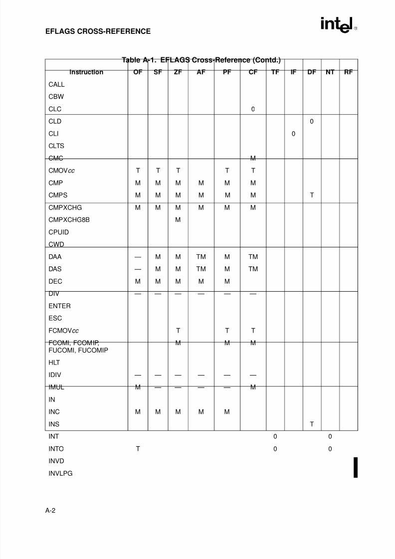
8/3/2019 Intel Architecture Software Developer's Manual, Volume 1: Basic Architecture
http://slidepdf.com/reader/full/intel-architecture-software-developers-manual-volume-1-basic-architecture 230/283
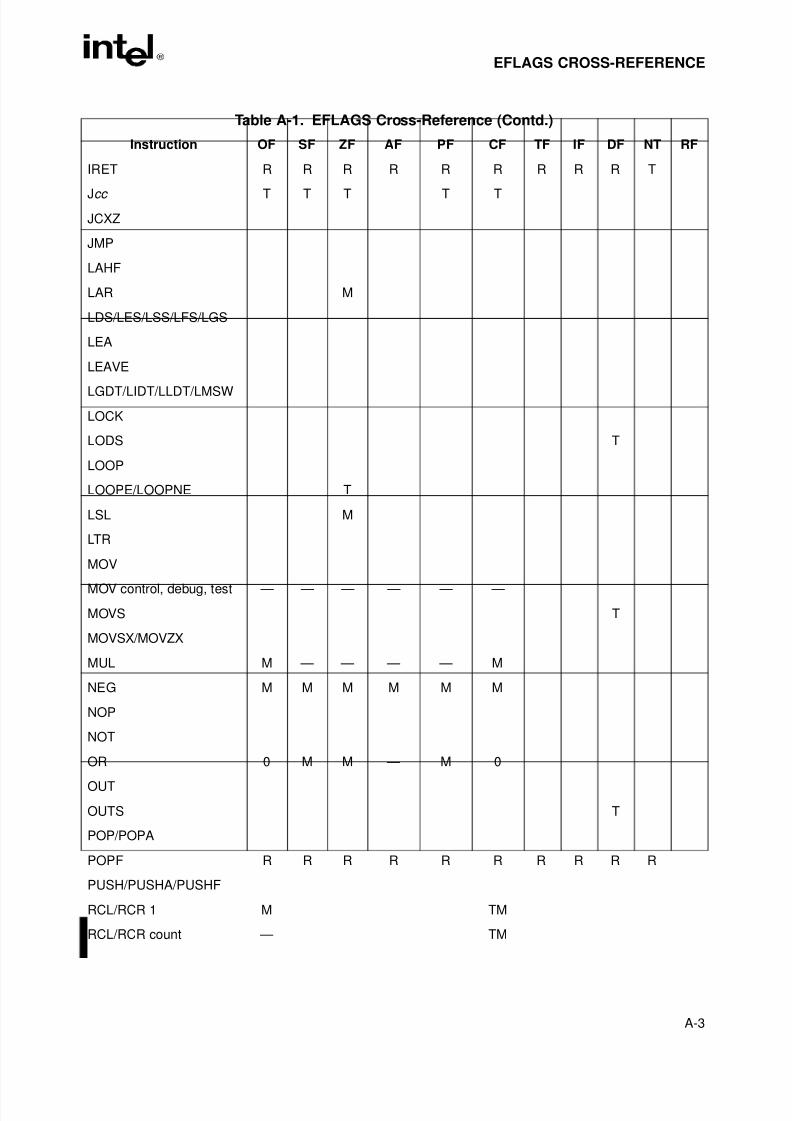
8/3/2019 Intel Architecture Software Developer's Manual, Volume 1: Basic Architecture
http://slidepdf.com/reader/full/intel-architecture-software-developers-manual-volume-1-basic-architecture 231/283
A-3
EFLAGS CROSS-REFERENCE
Instruction OF SF ZF AF PF CF TF IF DF NT RF
IRET R R R R R R R R R T
Jcc T T T T T
JCXZ
JMP
LAHF
LAR M
LDS/LES/LSS/LFS/LGS
LEA
LEAVE
LGDT/LIDT/LLDT/LMSW
LOCK
LODS T
LOOP
LOOPE/LOOPNE T
LSL M
LTR
MOV
MOV control, debug, test — — — — — —
MOVS T
MOVSX/MOVZX
MUL M — — — — M
NEG M M M M M M
NOP
NOT
OR 0 M M — M 0OUT
OUTS T
POP/POPA
POPF R R R R R R R R R R
PUSH/PUSHA/PUSHF
RCL/RCR 1 M TM
RCL/RCR count — TM
Table A-1. EFLAGS Cross-Reference (Contd.)
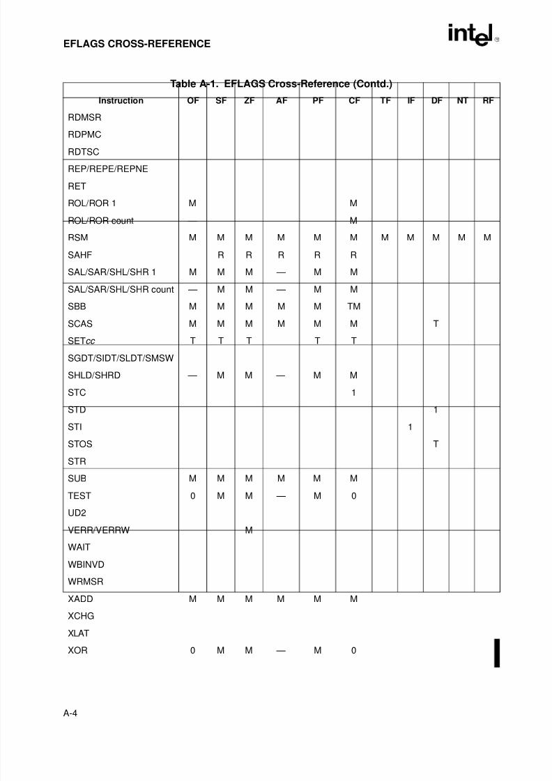
8/3/2019 Intel Architecture Software Developer's Manual, Volume 1: Basic Architecture
http://slidepdf.com/reader/full/intel-architecture-software-developers-manual-volume-1-basic-architecture 232/283
A-4
EFLAGS CROSS-REFERENCE
Instruction OF SF ZF AF PF CF TF IF DF NT RF
RDMSR
RDPMC
RDTSC
REP/REPE/REPNE
RET
ROL/ROR 1 M M
ROL/ROR count — M
RSM M M M M M M M M M M M
SAHF R R R R R
SAL/SAR/SHL/SHR 1 M M M — M M
SAL/SAR/SHL/SHR count — M M — M M
SBB M M M M M TM
SCAS M M M M M M T
SETcc T T T T T
SGDT/SIDT/SLDT/SMSW
SHLD/SHRD — M M — M M
STC 1
STD 1
STI 1
STOS T
STR
SUB M M M M M M
TEST 0 M M — M 0
UD2
VERR/VERRW M
WAIT
WBINVD
WRMSR
XADD M M M M M M
XCHG
XLAT
XOR 0 M M — M 0
Table A-1. EFLAGS Cross-Reference (Contd.)
8/3/2019 Intel Architecture Software Developer's Manual, Volume 1: Basic Architecture
http://slidepdf.com/reader/full/intel-architecture-software-developers-manual-volume-1-basic-architecture 233/283
BEFLAGSCondition Codes

8/3/2019 Intel Architecture Software Developer's Manual, Volume 1: Basic Architecture
http://slidepdf.com/reader/full/intel-architecture-software-developers-manual-volume-1-basic-architecture 234/283
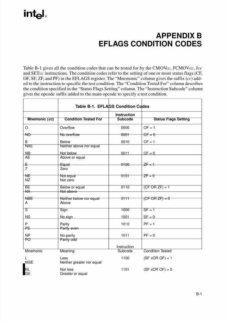
8/3/2019 Intel Architecture Software Developer's Manual, Volume 1: Basic Architecture
http://slidepdf.com/reader/full/intel-architecture-software-developers-manual-volume-1-basic-architecture 235/283
B-1
APPENDIX BEFLAGS CONDITION CODES
Table B-1 gives all the condition codes that can be tested for by the CMOVcc, FCMOVcc, Jccand SETcc instructions. The condition codes refer to the setting of one or more status flags (CF,OF, SF, ZF, and PF) in the EFLAGS register. The “Mnemonic” column gives the suffix (cc) add-ed to the instruction to specific the test condition. The “Condition Tested For” column describesthe condition specified in the “Status Flags Setting” column. The “Instruction Subcode” columngives the opcode suffix added to the main opcode to specify a test condition.
Table B-1. EFLAGS Condition Codes
Mnemonic (cc ) Condition Tested ForInstructionSubcode Status Flags Setting
O Overflow 0000 OF = 1
NO No overflow 0001 OF = 0
BNAE
BelowNeither above nor equal
0010 CF = 1
NBAE
Not belowAbove or equal
0011 CF = 0
EZ EqualZero 0100 ZF = 1
NENZ
Not equalNot zero
0101 ZF = 0
BENA
Below or equalNot above
0110 (CF OR ZF) = 1
NBEA
Neither below nor equalAbove
0111 (CF OR ZF) = 0
S Sign 1000 SF = 1
NS No sign 1001 SF = 0
PPE
ParityParity even
1010 PF = 1
NPPO
No parityParity odd
1011 PF = 0
Mnemonic MeaningInstructionSubcode Condition Tested
LNGE
LessNeither greater nor equal
1100 (SF xOR OF) = 1
NLGE
Not lessGreater or equal
1101 (SF xOR OF) = 0
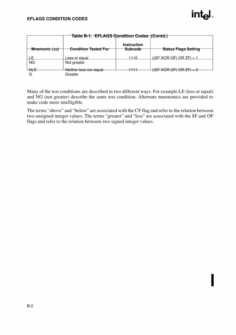
8/3/2019 Intel Architecture Software Developer's Manual, Volume 1: Basic Architecture
http://slidepdf.com/reader/full/intel-architecture-software-developers-manual-volume-1-basic-architecture 236/283
B-2
EFLAGS CONDITION CODES
Many of the test conditions are described in two different ways. For example LE (less or equal)and NG (not greater) describe the same test condition. Alternate mnemonics are provided tomake code more intelligible.
The terms “above” and “below” are associated with the CF flag and refer to the relation between
two unsigned integer values. The terms “greater” and “less” are associated with the SF and OFflags and refer to the relation between two signed integer values.
LENG
Less or equalNot greater
1110 ((SF XOR OF) OR ZF) = 1
NLEG
Neither less nor equalGreater
1111 ((SF XOR OF) OR ZF) = 0
Table B-1. EFLAGS Condition Codes (Contd.)
Mnemonic (cc ) Condition Tested ForInstructionSubcode Status Flags Setting
8/3/2019 Intel Architecture Software Developer's Manual, Volume 1: Basic Architecture
http://slidepdf.com/reader/full/intel-architecture-software-developers-manual-volume-1-basic-architecture 237/283
CFloating-PointExceptions Summary

8/3/2019 Intel Architecture Software Developer's Manual, Volume 1: Basic Architecture
http://slidepdf.com/reader/full/intel-architecture-software-developers-manual-volume-1-basic-architecture 238/283
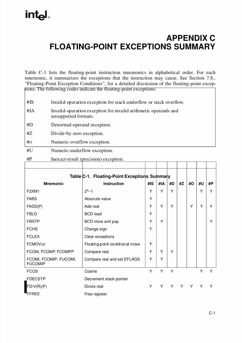
8/3/2019 Intel Architecture Software Developer's Manual, Volume 1: Basic Architecture
http://slidepdf.com/reader/full/intel-architecture-software-developers-manual-volume-1-basic-architecture 239/283
C-1
APPENDIX CFLOATING-POINT EXCEPTIONS SUMMARY
Table C-1 lists the floating-point instruction mnemonics in alphabetical order. For eachmnemonic, it summarizes the exceptions that the instruction may cause. See Section 7.8.,“Floating-Point Exception Conditions”, for a detailed discussion of the floating-point excep-tions. The following codes indicate the floating-point exceptions:
#IS Invalid-operation exception for stack underflow or stack overflow.
#IA Invalid-operation exception for invalid arithmetic operands and
unsupported formats.#D Denormal-operand exception.
#Z Divide-by-zero exception.
#O Numeric-overflow exception.
#U Numeric-underflow exception.
#P Inexact-result (precision) exception.
Table C-1. Floating-Point Exceptions SummaryMnemonic Instruction #IS #IA #D #Z #O #U #P
F2XM1 2X –1 Y Y Y Y Y
FABS Absolute value Y
FADD(P) Add real Y Y Y Y Y Y
FBLD BCD load Y
FBSTP BCD store and pop Y Y Y
FCHS Change sign Y
FCLEX Clear exceptions
FCMOVcc Floating-point conditional move Y
FCOM, FCOMP, FCOMPP Compare real Y Y Y
FCOMI, FCOMIP, FUCOMI,FUCOMIP
Compare real and set EFLAGS Y Y
FCOS Cosine Y Y Y Y Y
FDECSTP Decrement stack pointer
FDIV(R)(P) Divide real Y Y Y Y Y Y Y
FFREE Free register
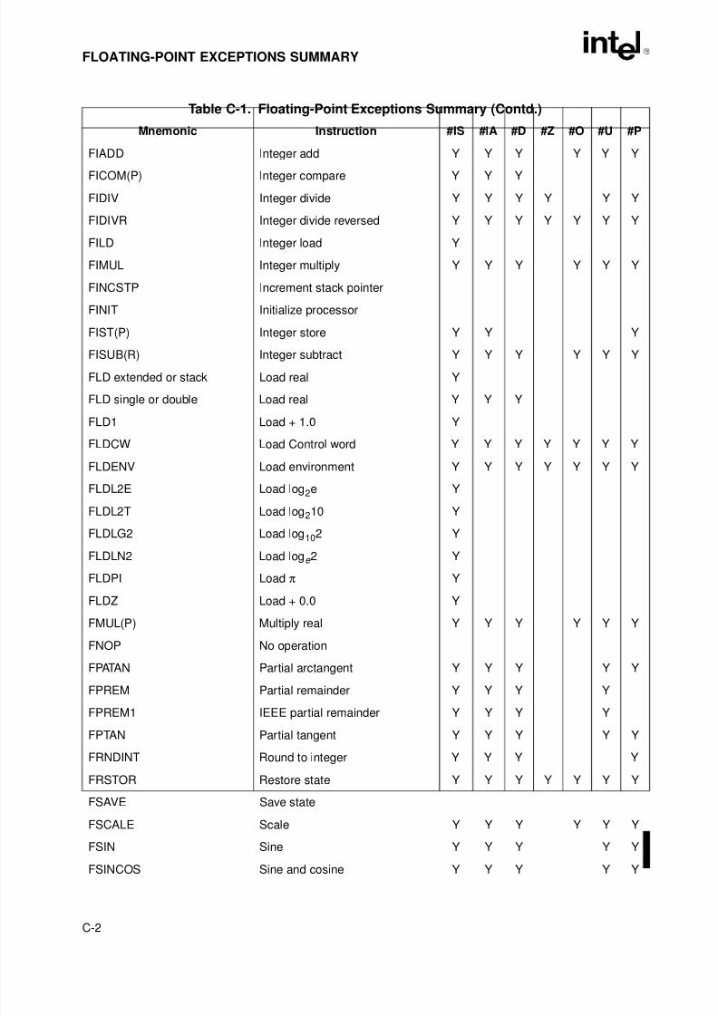
8/3/2019 Intel Architecture Software Developer's Manual, Volume 1: Basic Architecture
http://slidepdf.com/reader/full/intel-architecture-software-developers-manual-volume-1-basic-architecture 240/283
C-2
FLOATING-POINT EXCEPTIONS SUMMARY
Mnemonic Instruction #IS #IA #D #Z #O #U #P
FIADD Integer add Y Y Y Y Y Y
FICOM(P) Integer compare Y Y Y
FIDIV Integer divide Y Y Y Y Y Y
FIDIVR Integer divide reversed Y Y Y Y Y Y Y
FILD Integer load Y
FIMUL Integer multiply Y Y Y Y Y Y
FINCSTP Increment stack pointer
FINIT Initialize processor
FIST(P) Integer store Y Y Y
FISUB(R) Integer subtract Y Y Y Y Y Y
FLD extended or stack Load real Y
FLD single or double Load real Y Y Y
FLD1 Load + 1.0 Y
FLDCW Load Control word Y Y Y Y Y Y Y
FLDENV Load environment Y Y Y Y Y Y Y
FLDL2E Load log2e Y
FLDL2T Load log210 Y
FLDLG2 Load log102 Y
FLDLN2 Load loge 2 Y
FLDPI Load π Y
FLDZ Load + 0.0 Y
FMUL(P) Multiply real Y Y Y Y Y Y
FNOP No operation
FPATAN Partial arctangent Y Y Y Y Y
FPREM Partial remainder Y Y Y YFPREM1 IEEE partial remainder Y Y Y Y
FPTAN Partial tangent Y Y Y Y Y
FRNDINT Round to integer Y Y Y Y
FRSTOR Restore state Y Y Y Y Y Y Y
FSAVE Save state
FSCALE Scale Y Y Y Y Y Y
FSIN Sine Y Y Y Y Y
FSINCOS Sine and cosine Y Y Y Y Y
Table C-1. Floating-Point Exceptions Summary (Contd.)
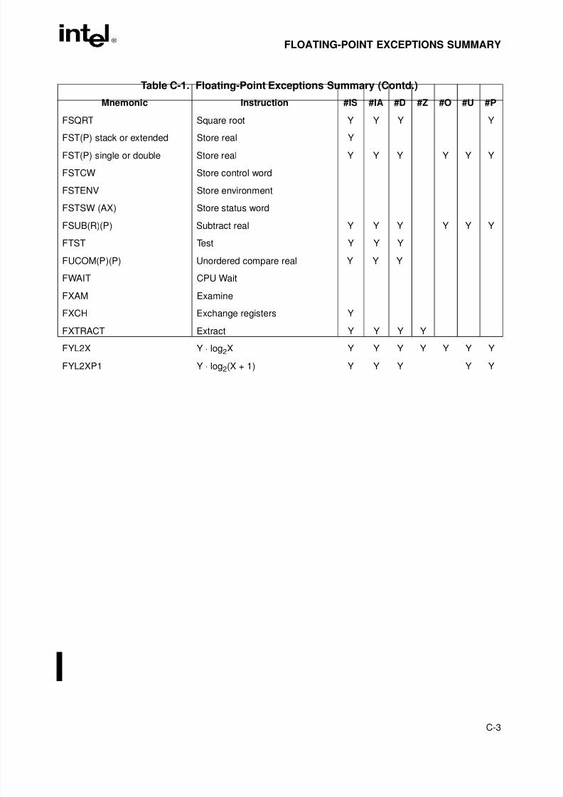
8/3/2019 Intel Architecture Software Developer's Manual, Volume 1: Basic Architecture
http://slidepdf.com/reader/full/intel-architecture-software-developers-manual-volume-1-basic-architecture 241/283
C-3
FLOATING-POINT EXCEPTIONS SUMMARY
Mnemonic Instruction #IS #IA #D #Z #O #U #P
FSQRT Square root Y Y Y Y
FST(P) stack or extended Store real Y
FST(P) single or double Store real Y Y Y Y Y Y
FSTCW Store control word
FSTENV Store environment
FSTSW (AX) Store status word
FSUB(R)(P) Subtract real Y Y Y Y Y Y
FTST Test Y Y Y
FUCOM(P)(P) Unordered compare real Y Y Y
FWAIT CPU Wait
FXAM Examine
FXCH Exchange registers Y
FXTRACT Extract Y Y Y Y
FYL2X Y ⋅ log2X Y Y Y Y Y Y Y
FYL2XP1 Y ⋅ log2(X + 1) Y Y Y Y Y
Table C-1. Floating-Point Exceptions Summary (Contd.)

8/3/2019 Intel Architecture Software Developer's Manual, Volume 1: Basic Architecture
http://slidepdf.com/reader/full/intel-architecture-software-developers-manual-volume-1-basic-architecture 242/283
8/3/2019 Intel Architecture Software Developer's Manual, Volume 1: Basic Architecture
http://slidepdf.com/reader/full/intel-architecture-software-developers-manual-volume-1-basic-architecture 243/283
DGuidelines forWriting FPU
Exception Handlers

8/3/2019 Intel Architecture Software Developer's Manual, Volume 1: Basic Architecture
http://slidepdf.com/reader/full/intel-architecture-software-developers-manual-volume-1-basic-architecture 244/283
8/3/2019 Intel Architecture Software Developer's Manual, Volume 1: Basic Architecture
http://slidepdf.com/reader/full/intel-architecture-software-developers-manual-volume-1-basic-architecture 245/283
D-1
APPENDIX DGUIDELINES FOR WRITING FPU
EXCEPTION HANDLERS
As described in Chapter 7, Floating-Point Unit , the Intel Architecture supports two mechanismsfor accessing exception handlers to handle unmasked FPU exceptions: native mode and MS-DOS compatibility mode. The primary purpose of this appendix is to provide detailed informa-tion to help software engineers design and write FPU exception-handling facilities to run on PCsystems that use the MS-DOS compatibility mode1 for handling FPU exceptions. Some of theinformation in this appendix will also be of interest to engineers who are writing native-modeFPU exception handlers. The information provided is as follows:
• Discussion of the origin of the MS-DOS* FPU exception handling mechanism and itsrelationship to the FPU’s native exception handling mechanism.
• Description of the Intel Architecture flags and processor pins that control the MS-DOSFPU exception handling mechanism.
• Description of the external hardware typically required to support MS-DOS exceptionhandling mechanism.
• Description of the FPU’s exception handling mechanism and the typical protocol for FPUexception handlers.
• Code examples that demonstrate various levels of FPU exception handlers.
• Discussion of FPU considerations in multitasking environments.
• Discussion of native mode FPU exception handling.
The information given is oriented toward the most recent generations of Intel architectureprocessors, starting with the Intel486. It is intended to augment the reference information givenin Chapter 7, Floating-Point Unit .
A more extensive version of this appendix is available in the application note AP-578, Software
and Hardware Considerations for FPU Exception Handlers for Intel Architecture Processors
(Order Number 242415-001), which is available from Intel.
1. Microsoft Windows* 95 and Windows* 3.1 (and earlier versions) operating systems use almost the sameFPU exception handling interface as the operating system. The recommendations in this appendix for a
MS-DOS* compatible exception handler thus apply to all three operating systems.
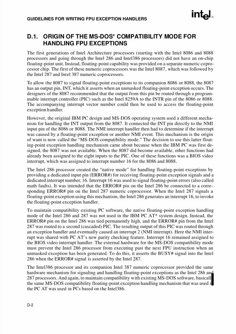
8/3/2019 Intel Architecture Software Developer's Manual, Volume 1: Basic Architecture
http://slidepdf.com/reader/full/intel-architecture-software-developers-manual-volume-1-basic-architecture 246/283
D-2
GUIDELINES FOR WRITING FPU EXCEPTION HANDLERS
D.1. ORIGIN OF THE MS-DOS* COMPATIBILITY MODE FORHANDLING FPU EXCEPTIONS
The first generations of Intel Architecture processors (starting with the Intel 8086 and 8088
processors and going through the Intel 286 and Intel386 processors) did not have an on-chipfloating-point unit. Instead, floating-point capability was provided on a separate numeric copro-cessor chip. The first of these numeric coprocessors was the Intel 8087, which was followed bythe Intel 287 and Intel 387 numeric coprocessors.
To allow the 8087 to signal floating-point exceptions to its companion 8086 or 8088, the 8087has an output pin, INT, which it asserts when an unmasked floating-point exception occurs. Thedesigners of the 8087 recommended that the output from this pin be routed through a program-mable interrupt controller (PIC) such as the Intel 8259A to the INTR pin of the 8086 or 8088.The accompanying interrupt vector number could then be used to access the floating-pointexception handler.
However, the original IBM PC design and MS-DOS operating system used a different mecha-nism for handling the INT output from the 8087. It connected the INT pin directly to the NMIinput pin of the 8086 or 8088. The NMI interrupt handler then had to determine if the interruptwas caused by a floating-point exception or another NMI event. This mechanism is the originof want is now called the “MS-DOS compatibility mode.” The decision to use this latter float-ing-point exception handling mechanism came about because when the IBM PC was first de-signed, the 8087 was not available. When the 8087 did become available, other functions hadalready been assigned to the eight inputs to the PIC. One of these functions was a BIOS videointerrupt, which was assigned to interrupt number 16 for the 8086 and 8088.
The Intel 286 processor created the “native mode” for handling floating-point exceptions byproviding a dedicated input pin (ERROR#) for receiving floating-point exception signals and adedicated interrupt number, 16. Interrupt 16 was used to signal floating-point errors (also calledmath faults). It was intended that the ERROR# pin on the Intel 286 be connected to a corre-sponding ERROR# pin on the Intel 287 numeric coprocessor. When the Intel 287 signals afloating-point exception using this mechanism, the Intel 286 generates an interrupt 16, to invokethe floating-point exception handler.
To maintain compatibility existing PC software, the native floating-point exception handlingmode of the Intel 286 and 287 was not used in the IBM PC AT* system design. Instead, theERROR# pin on the Intel 286 was tied permanently high, and the ERROR# pin from the Intel287 was routed to a second (cascaded) PIC. The resulting output of this PIC was routed throughan exception handler and eventually caused an interrupt 2 (NMI interrupt). Here the NMI inter-rupt was shared with PC AT’s new parity checking feature. Interrupt 16 remained assigned tothe BIOS video interrupt handler. The external hardware for the MS-DOS compatibility modemust prevent the Intel 286 processor from executing past the next FPU instruction when anunmasked exception has been generated. To do this, it asserts the BUSY# signal into the Intel286 when the ERROR# signal is asserted by the Intel 287.
The Intel386 processor and its companion Intel 387 numeric coprocessor provided the samehardware mechanism for signaling and handling floating-point exceptions as the Intel 286 and287 processors. And again, to maintain compatibility with existing MS-DOS software, basicallythe same MS-DOS compatibility floating-point exception handling mechanism that was used inthe PC AT was used in PCs based on the Intel386.
8/3/2019 Intel Architecture Software Developer's Manual, Volume 1: Basic Architecture
http://slidepdf.com/reader/full/intel-architecture-software-developers-manual-volume-1-basic-architecture 247/283
D-3
GUIDELINES FOR WRITING FPU EXCEPTION HANDLERS
D.2. IMPLEMENTATION OF THE MS-DOS* COMPATIBILITY MODEIN THE INTEL486™, PENTIUM ® , AND PENTIUM PROPROCESSORS
Beginning with the Intel486 processor, the Intel Architecture provided a dedicated mechanismfor enabling the MS-DOS compatibility mode for FPU exceptions and for generating externalFPU-exception signals while operating in this mode. The following sections describe the imple-mentation of the MS-DOS compatibility mode in Intel486 and Pentium processors and in thePentium Pro processor. Also described is the recommended external hardware to support thismode of operation.
D.2.1. MS-DOS* Compatibility Mode in the Intel486™ andPentium ® Processors
In the Intel486, several things were done to enhance and speed up the numeric coprocessor, nowcalled the floating-point unit (FPU). The most important enhancement was that the FPU wasincluded in the same chip as the processor, for increased speed in FPU computations andreduced latency for FPU exception handling. Also, for the first time, the MS-DOS compatibilitymode was built into the chip design, with the addition of the NE bit in control register CR0 andthe addition of the FERR# (Floating point ERRor) and IGNNE# (IGNore Numeric Error) pins.
The NE bit selects the native FPU exception handling mode (NE = 1) or the MS-DOS compat-ibility mode (NE = 0). When native mode is selected, all signaling of floating-point exceptionsis handled internally in the Intel486 chip, resulting in the generation of an interrupt 16.
When MS-DOS compatibility mode is selected the FERRR# and IGNNE# pins are used tosignal floating-point exceptions. The FERR# output pin, which replaces the ERROR# pin fromthe previous generations of Intel Architecture numeric coprocessors, is connected to a PIC. Anew input signal, IGNNE#, is provided to allow the FPU exception handler to execute FPUinstructions, if desired, without first clearing the error condition and without triggering the inter-rupt a second time. This IGNNE# feature is needed to replicate the capability that was providedon MS-DOS compatibility Intel 286 and Intel 287 and Intel386 and Intel 387 systems by turningoff the BUSY# signal, when inside the FPU exception handler, before clearing the error condi-tion.
Note that Intel, in order to provide Intel486 processors for market segments which had no needfor an FPU, created the “SX” versions. These Intel486 SX processors did not contain the floatingpoint unit. Intel also produced Intel 487 SX processors for end users who later decided toupgrade to a system with an FPU. These Intel 487 SX processors are similar to standard Intel486processors with a working FPU on board. Thus, the external circuitry necessary to support theMS-DOS compatibility mode for Intel 487 SX processors is the same as for standard Intel486DX processors.
The Pentium and Pentium Pro processors offer the same mechanism (the NE bit and the FERR#and IGNNE# pins) as the Intel486 processors for generating FPU exceptions in MS-DOScompatibility mode. The actions of these mechanisms are slightly different and more straight-
8/3/2019 Intel Architecture Software Developer's Manual, Volume 1: Basic Architecture
http://slidepdf.com/reader/full/intel-architecture-software-developers-manual-volume-1-basic-architecture 248/283
D-4
GUIDELINES FOR WRITING FPU EXCEPTION HANDLERS
forward for the Pentium Pro processors, as described in Section D.2.2., “MS-DOS* Compati-bility Mode in the Pentium® Pro Processor”.
For Pentium and Pentium Pro processors, it is important to note that the special DP (Dual
Processing) mode for Pentium Processors and also the more general Intel MultiProcessor Spec-ification for systems with multiple Pentium or Pentium Pro processors support FPU exceptionhandling only in the native mode. Intel does not recommend using the MS-DOS compatibilityFPU mode for systems using more than one processor.
D.2.1.1. BASIC RULES: WHEN FERR# IS GENERATED
When MS-DOS compatibility mode is enabled for the Intel486 or Pentium processors (NE bitis set to 0) and the IGNNE# input pin is de-asserted, the FERR# signal is generated as follows:
1. When an FPU instruction causes an unmasked FPU exception, the processor (in most
cases) uses a “deferred” method of reporting the error. This means that the processor doesnot respond immediately, but rather freezes just before executing the next WAIT or FPUinstruction (except for “no-wait” instructions, which the FPU executes regardless of anerror condition).
2. When the processor freezes, it also asserts the FERR# output.
3. The frozen processor waits for an external interrupt, which must be supplied by externalhardware in response to the FERR# assertion.
4. In MS-DOS* compatibility systems, FERR# is fed to the IRQ13 input in the cascaded PIC.The PIC generates interrupt 75H, which then branches to interrupt 2, as described earlier in
this appendix for systems using the Intel 286 and Intel 287 or Intel386 and Intel 387processors.
The deferred method of error reporting is used for all exceptions caused by the basic arithmeticinstructions (including FADD, FSUB, FMUL, FDIV, FSQRT, FCOM and FUCOM), for preci-sion exceptions caused by all types of FPU instructions, and for numeric underflow and over-flow exceptions caused by all types of FPU instructions except stores to memory.
Some FPU instructions with some FPU exceptions use an “immediate” method of reportingerrors. Here, the FERR# is asserted immediately, at the time that the exception occurs. Theimmediate method of error reporting is used for FPU stack fault, invalid operation and denormalexceptions caused by all transcendental instructions, FSCALE, FXTRACT, FPREM and others,and all exceptions (except precision) when caused by FPU store instructions. Like deferred errorreporting, immediate error reporting will cause the processor to freeze just before executing thenext WAIT or FPU instruction if the error condition has not been cleared by that time.
Note that in general, whether deferred or immediate error reporting is used for an FPU exceptiondepends both on which exception occurred and which instruction caused that exception. A com-plete specification of these cases, which applies to both the Pentium and the Intel486 processors,is given in Section 5.1.21 in the Pentium® Processor Family Developer’s Manual: Volume 1.
8/3/2019 Intel Architecture Software Developer's Manual, Volume 1: Basic Architecture
http://slidepdf.com/reader/full/intel-architecture-software-developers-manual-volume-1-basic-architecture 249/283
D-5
GUIDELINES FOR WRITING FPU EXCEPTION HANDLERS
If NE=0 but the IGNNE# input is active while an unmasked FPU exception is in effect, theprocessor disregards the exception, does not assert FERR#, and continues. If IGNNE# is thende-asserted and the FPU exception has not been cleared, the processor will respond as describedabove. (That is, an immediate exception case will assert FERR# immediately. A deferred excep-
tion case will assert FERR# and freeze just before the next FPU or WAIT instruction.) The asser-tion of IGNNE# is intended for use only inside the FPU exception handler, where it is needed if one wants to execute non-control FPU instructions for diagnosis, before clearing the exceptioncondition. When IGNNE# is asserted inside the exception handler, a preceding FPU exceptionhas already caused FERR# to be asserted, and the external interrupt hardware has responded,but IGNNE# assertion still prevents the freeze at FPU instructions. Note that if IGNNE# is leftactive outside of the FPU exception handler, additional FPU instructions may be executed aftera given instruction has caused an FPU exception. In this case, if the FPU exception handler everdid get invoked, it could not determine which instruction caused the exception.
To properly manage the interface between the processor’s FERR# output, its IGNNE# input, and
the IRQ13 input of the PIC, additional external hardware is needed. A recommended configu-ration is described in the following section.
D.2.1.2. RECOMMENDED EXTERNAL HARDWARE TO SUPPORT THE
MS-DOS* COMPATIBILITY MODE
Figure D-1 provides an external circuit that will assure proper handling of FERR# and IGNNE#when an FPU exception occurs. In particular, it assures that IGNNE# will be active only insidethe FPU exception handler without depending on the order of actions by the exception handler.Some hardware implementations have been less robust because they have depended on the
exception handler to clear the FPU exception interrupt request to the PIC (FP_IRQ signal)before the handler causes FERR# to be de-asserted by clearing the exception from the FPUitself. Figure D-2 shows the details of how IGNNE# will behave when the circuit in FigureD-1 is implemented. The temporal regions within the FPU exception handler activity aredescribed as follows:
1. The FERR# signal is activated by an FPU exception and sends an interrupt request throughthe PIC to the processor’s INTR pin.
2. During the FPU interrupt service routine (exception handler) the processor will need toclear the interrupt request latch (Flip Flop #1). It may also want to execute non-controlFPU instructions before the exception is cleared from the FPU. For this purpose the
IGNNE# must be driven low. Typically in the PC environment an I/O access to Port 0F0Hclears the external FPU exception interrupt request (FP_IRQ). In the recommended circuit,this access also is used to activate IGNNE#. With IGNNE# active the FPU exceptionhandler may execute any FPU instruction without being blocked by an active FPUexception.
3. Clearing the exception within the FPU will cause the FERR# signal to be deactivated andthen there is no further need for IGNNE# to be active. In the recommended circuit, thedeactivation of FERR# is used to deactivate IGNNE#. If another circuit is used, thesoftware and circuit together must assure that IGNNE# is deactivated no later than the exitfrom the FPU exception handler.
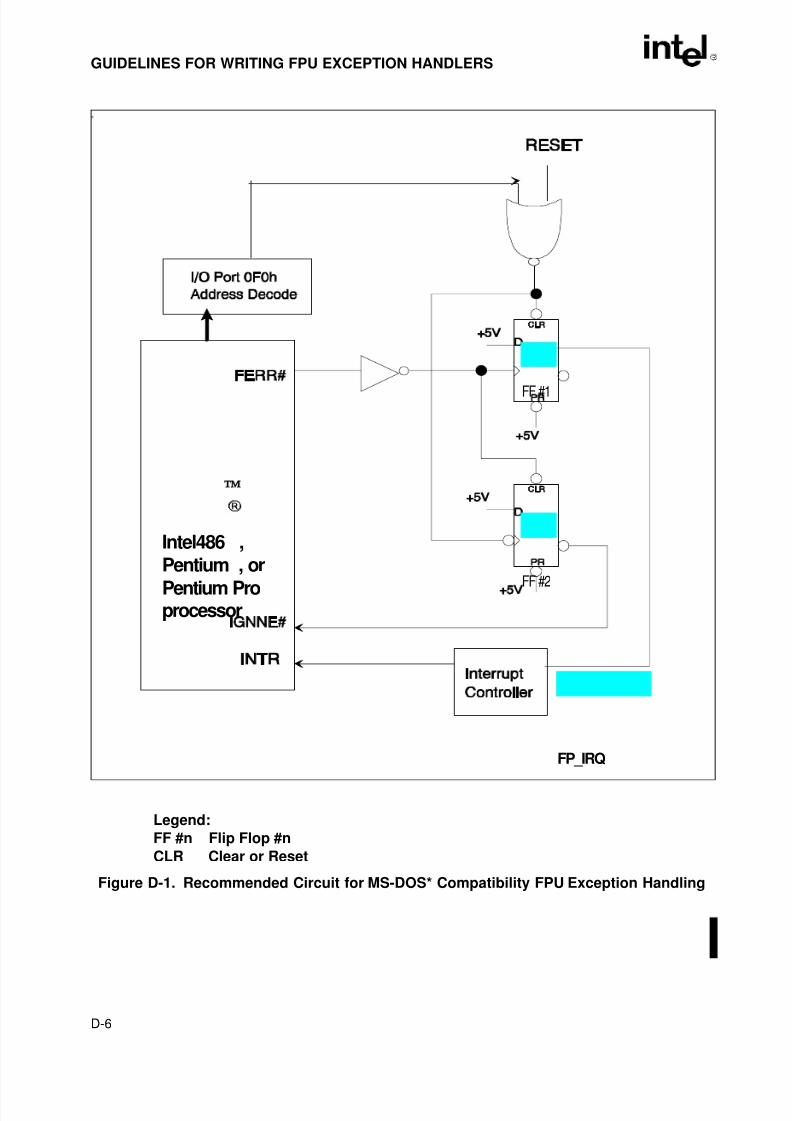
8/3/2019 Intel Architecture Software Developer's Manual, Volume 1: Basic Architecture
http://slidepdf.com/reader/full/intel-architecture-software-developers-manual-volume-1-basic-architecture 250/283
D-6
GUIDELINES FOR WRITING FPU EXCEPTION HANDLERS
*
Figure D-1. Recommended Circuit for MS-DOS* Compatibility FPU Exception Handling
Intel486™,
Pentium
, or
Pentium Proprocessor
FF #1
FF #2
FP_IRQ
Legend:
FF #n Flip Flop #n
CLR Clear or Reset
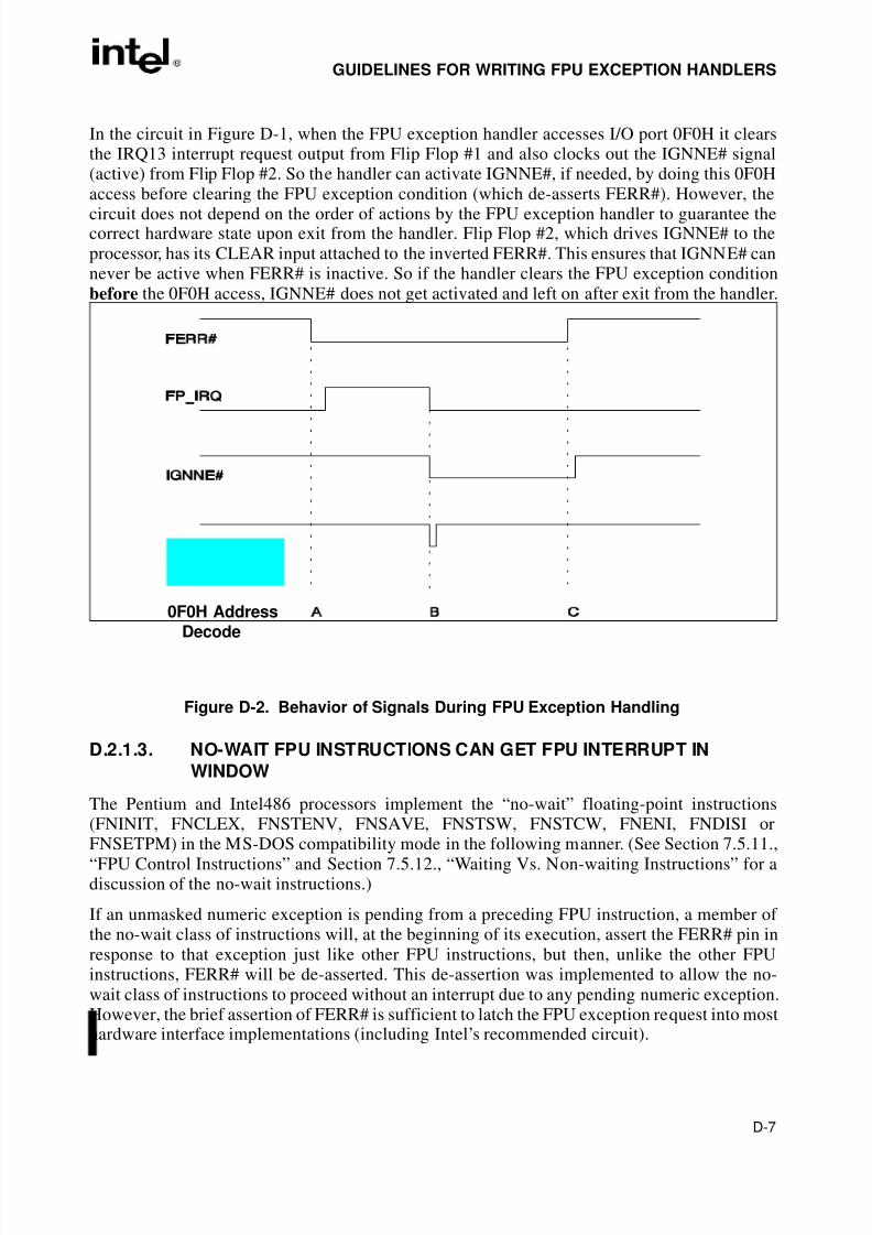
8/3/2019 Intel Architecture Software Developer's Manual, Volume 1: Basic Architecture
http://slidepdf.com/reader/full/intel-architecture-software-developers-manual-volume-1-basic-architecture 251/283
D-7
GUIDELINES FOR WRITING FPU EXCEPTION HANDLERS
In the circuit in Figure D-1, when the FPU exception handler accesses I/O port 0F0H it clearsthe IRQ13 interrupt request output from Flip Flop #1 and also clocks out the IGNNE# signal(active) from Flip Flop #2. So the handler can activate IGNNE#, if needed, by doing this 0F0Haccess before clearing the FPU exception condition (which de-asserts FERR#). However, the
circuit does not depend on the order of actions by the FPU exception handler to guarantee thecorrect hardware state upon exit from the handler. Flip Flop #2, which drives IGNNE# to theprocessor, has its CLEAR input attached to the inverted FERR#. This ensures that IGNNE# cannever be active when FERR# is inactive. So if the handler clears the FPU exception condition
before the 0F0H access, IGNNE# does not get activated and left on after exit from the handler.
D.2.1.3. NO-WAIT FPU INSTRUCTIONS CAN GET FPU INTERRUPT IN
WINDOW
The Pentium and Intel486 processors implement the “no-wait” floating-point instructions(FNINIT, FNCLEX, FNSTENV, FNSAVE, FNSTSW, FNSTCW, FNENI, FNDISI or
FNSETPM) in the MS-DOS compatibility mode in the following manner. (See Section 7.5.11.,“FPU Control Instructions” and Section 7.5.12., “Waiting Vs. Non-waiting Instructions” for adiscussion of the no-wait instructions.)
If an unmasked numeric exception is pending from a preceding FPU instruction, a member of the no-wait class of instructions will, at the beginning of its execution, assert the FERR# pin inresponse to that exception just like other FPU instructions, but then, unlike the other FPUinstructions, FERR# will be de-asserted. This de-assertion was implemented to allow the no-wait class of instructions to proceed without an interrupt due to any pending numeric exception.However, the brief assertion of FERR# is sufficient to latch the FPU exception request into mosthardware interface implementations (including Intel’s recommended circuit).
Figure D-2. Behavior of Signals During FPU Exception Handling
0F0H Address
Decode
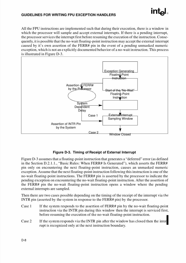
8/3/2019 Intel Architecture Software Developer's Manual, Volume 1: Basic Architecture
http://slidepdf.com/reader/full/intel-architecture-software-developers-manual-volume-1-basic-architecture 252/283
D-8
GUIDELINES FOR WRITING FPU EXCEPTION HANDLERS
All the FPU instructions are implemented such that during their execution, there is a window inwhich the processor will sample and accept external interrupts. If there is a pending interrupt,the processor services the interrupt first before resuming the execution of the instruction. Conse-quently, it is possible that the no-wait floating-point instruction may accept the external interrupt
caused by it’s own assertion of the FERR# pin in the event of a pending unmasked numericexception, which is not an explicitly documented behavior of a no-wait instruction. This processis illustrated in Figure D-3.
Figure D-3 assumes that a floating-point instruction that generates a “deferred” error (as definedin the Section D.2.1.1., “Basic Rules: When FERR# Is Generated”), which asserts the FERR#pin only on encountering the next floating-point instruction, causes an unmasked numericexception. Assume that the next floating-point instruction following this instruction is one of theno-wait floating-point instructions. The FERR# pin is asserted by the processor to indicate the
pending exception on encountering the no-wait floating-point instruction. After the assertion of the FERR# pin the no-wait floating-point instruction opens a window where the pendingexternal interrupts are sampled.
Then there are two cases possible depending on the timing of the receipt of the interrupt via theINTR pin (asserted by the system in response to the FERR# pin) by the processor.
Case 1 If the system responds to the assertion of FERR# pin by the no-wait floating-pointinstruction via the INTR pin during this window then the interrupt is serviced first,before resuming the execution of the no-wait floating-point instruction.
Case 2 If the system responds via the INTR pin after the window has closed then the inter-
rupt is recognized only at the next instruction boundary.
Figure D-3. Timing of Receipt of External Interrupt
Assertion of FERR#
Exception GeneratingFloating-Point
Instruction
by the Processor
System
Assertion of INTR Pinby the System
Case 1
Case 2
Start of the “No-Wait”Floating-Point
Instruction
External InterruptSampling Window
Window Closed
DependentDelay
8/3/2019 Intel Architecture Software Developer's Manual, Volume 1: Basic Architecture
http://slidepdf.com/reader/full/intel-architecture-software-developers-manual-volume-1-basic-architecture 253/283
D-9
GUIDELINES FOR WRITING FPU EXCEPTION HANDLERS
There are two other ways, in addition to Case 1 above, in which a no-wait floating-point instruc-tion can service a numeric exception inside its interrupt window. First, the first floating-pointerror condition could be of the “immediate” category (as defined in Section D.2.1.1., “BasicRules: When FERR# Is Generated”) that asserts FERR# immediately. If the system delay before
asserting INTR is long enough, relative to the time elapsed before the no-wait floating-point in-struction, INTR can be asserted inside the interrupt window for the latter. Second, consider twono-wait FPU instructions in close sequence, and assume that a previous FPU instruction hascaused an unmasked numeric exception. Then if the INTR timing is too long for an FERR# sig-nal triggered by the first no-wait instruction to hit the first instruction’s interrupt window, itcould catch the interrupt window of the second.
The possible malfunction of a no-wait FPU instruction explained above cannot happen if the in-struction is being used in the manner for which Intel originally designed it. The no-wait instruc-tions were intended to be used inside the FPU exception handler, to allow manipulation of theFPU before the error condition is cleared, without hanging the processor because of the FPU er-
ror condition, and without the need to assert IGNNE#. They will perform this function correctly,since before the error condition is cleared, the assertion of FERR# that caused the FPU errorhandler to be invoked is still active. Thus the logic that would assert FERR# briefly at a no-waitinstruction causes no change since FERR# is already asserted. The no-wait instructions may alsobe used without problem in the handler after the error condition is cleared, since now they willnot cause FERR# to be asserted at all.
If a no-wait instruction is used outside of the FPU exception handler, it may malfunction as ex-plained above, depending on the details of the hardware interface implementation and whichparticular processor is involved. The actual interrupt inside the window in the no-wait instruc-tion may be blocked by surrounding it with the instructions: PUSHFD, CLI, no-wait, then
POPFD. (CLI blocks interrupts, and the push and pop of flags preserves and restores the originalvalue of the interrupt flag.) However, if FERR# was triggered by the no-wait, its latched valueand the PIC response will still be in effect. Further code can be used to check for and correctsuch a condition, if needed. Section D.3.6., “Considerations When FPU Shared Between Tasks”,discusses an important example of this type of problem and gives a solution.
D.2.2. MS-DOS* Compatibility Mode in the Pentium ® ProProcessor
When bit NE=0 in CR0, the MS-DOS compatibility mode of the Pentium Pro processor providesFERR# and IGNNE# functionality that is almost identical to the Intel486 and Pentium proces-sors. The same external hardware described in Section D.2.1.2., “Recommended External Hard-ware to Support the MS-DOS* Compatibility Mode”, is recommended for the Pentium Proprocessor as well as the two previous generations. The only change to MS-DOS compatibilityFPU exception handling with the Pentium Pro processor is that all exceptions for all FPUinstructions cause immediate error reporting. That is, FERR# is asserted as soon as the FPUdetects an unmasked exception; there are no cases in which error reporting is deferred to the nextFPU or WAIT instruction. (As is discussed in Section D.2.1.1., “Basic Rules: When FERR# IsGenerated”, most exception cases in the Intel486 and Pentium processors are of the deferredtype.)
8/3/2019 Intel Architecture Software Developer's Manual, Volume 1: Basic Architecture
http://slidepdf.com/reader/full/intel-architecture-software-developers-manual-volume-1-basic-architecture 254/283
D-10
GUIDELINES FOR WRITING FPU EXCEPTION HANDLERS
Although FERR# is asserted immediately upon detection of an unmasked FPU error, thiscertainly does not mean that the requested interrupt will always be serviced before the nextinstruction in the code sequence is executed. To begin with, the Pentium Pro processor executesseveral instructions simultaneously. There also will be a delay, which depends on the external
hardware implementation, between the FERR# assertion from the processor and the respondingINTR assertion to the processor. Further, the interrupt request to the PICs (IRQ13) may betemporarily blocked by the operating system, or delayed by higher priority interrupts, andprocessor response to INTR itself is blocked if the operating system has cleared the IF bit inEFLAGS.
However, just as with the Intel486 and Pentium processors, if the IGNNE# input is inactive, afloating point exception which occurred in the previous FPU instruction and is unmasked causesthe processor to freeze immediately when encountering the next WAIT or FPU instruction (ex-cept for no-wait instructions). This means that if the FPU exception handler has not already beeninvoked due to the earlier exception (and therefore, the handler not has cleared that exception
state from the FPU), the processor is forced to wait for the handler to be invoked and handle theexception, before the processor can execute another WAIT or FPU instruction.
As explained in Section D.2.1.3., “No-Wait FPU Instructions Can Get FPU Interrupt inWindow”, if a no-wait instruction is used outside of the FPU exception handler, in the Intel486and Pentium processors, it may accept an unmasked exception from a previous FPU instructionwhich happens to fall within the external interrupt sampling window that is opened near thebeginning of execution of all FPU instructions. This will not happen in the Pentium Proprocessor, because this sampling window has been removed from the no-wait group of FPUinstructions.
D.3. RECOMMENDED PROTOCOL FOR MS-DOS*COMPATIBILITY HANDLERS
The activities of numeric programs can be split into two major areas: program control and arith-metic. The program control part performs activities such as deciding what functions to perform,calculating addresses of numeric operands, and loop control. The arithmetic part simply adds,subtracts, multiplies, and performs other operations on the numeric operands. The processor isdesigned to handle these two parts separately and efficiently. An FPU exception handler, if asystem chooses to implement one, is often one of the most complicated parts of the program
control code.
D.3.1. Floating-Point Exceptions and Their Defaults
The FPU can recognize six classes of floating-point exception conditions while executingfloating-point instructions:
1. #I — Invalid operation#IS — Stack fault#IA — IEEE standard invalid operation
8/3/2019 Intel Architecture Software Developer's Manual, Volume 1: Basic Architecture
http://slidepdf.com/reader/full/intel-architecture-software-developers-manual-volume-1-basic-architecture 255/283
D-11
GUIDELINES FOR WRITING FPU EXCEPTION HANDLERS
2. #Z — Divide-by-zero
3. #D — Denormalized operand
4. #O — Numeric overflow
5. #U — Numeric underflow
6. #P — Inexact result (precision)
For complete details on these exceptions and their defaults, see Section 7.7., “Floating-PointException Handling” and Section 7.8., “Floating-Point Exception Conditions”.
D.3.2. Two Options for Handling Numeric Exceptions
Depending on options determined by the software system designer, the processor takes one of
two possible courses of action when a numeric exception occurs:
• The FPU can handle selected exceptions itself, producing a default fix-up that isreasonable in most situations. This allows the numeric program execution to continueundisturbed. Programs can mask individual exception types to indicate that the FPU shouldgenerate this safe, reasonable result whenever the exception occurs. The default exceptionfix-up activity is treated by the FPU as part of the instruction causing the exception; noexternal indication of the exception is given (except that the instruction takes longer toexecute when it handles a masked exception.) When masked exceptions are detected, aflag is set in the numeric status register, but no information is preserved regarding where orwhen it was set.
• Alternatively, a software exception handler can be invoked to handle the exception. Whena numeric exception is unmasked and the exception occurs, the FPU stops furtherexecution of the numeric instruction and causes a branch to a software exception handler.The exception handler can then implement any sort of recovery procedures desired for anynumeric exception detectable by the FPU.
D.3.2.1. AUTOMATIC EXCEPTION HANDLING: USING MASKED
EXCEPTIONS
Each of the six exception conditions described above has a corresponding flag bit in the FPUstatus word and a mask bit in the FPU control word. If an exception is masked (the corre-sponding mask bit in the control word = 1), the processor takes an appropriate default action andcontinues with the computation. The processor has a default fix-up activity for every possibleexception condition it may encounter. These masked-exception responses are designed to besafe and are generally acceptable for most numeric applications.
For example, if the Inexact result (Precision) exception is masked, the system can specifywhether the FPU should handle a result that cannot be represented exactly by one of four modesof rounding: rounding it normally, chopping it toward zero, always rounding it up, or alwaysdown. If the Underflow exception is masked, the FPU will store a number that is too small to berepresented in normalized form as a denormal (or zero if it’s smaller than the smallestdenormal). Note that when exceptions are masked, the FPU may detect multiple exceptions in a
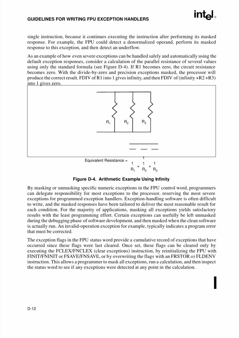
8/3/2019 Intel Architecture Software Developer's Manual, Volume 1: Basic Architecture
http://slidepdf.com/reader/full/intel-architecture-software-developers-manual-volume-1-basic-architecture 256/283
D-12
GUIDELINES FOR WRITING FPU EXCEPTION HANDLERS
single instruction, because it continues executing the instruction after performing its maskedresponse. For example, the FPU could detect a denormalized operand, perform its maskedresponse to this exception, and then detect an underflow.
As an example of how even severe exceptions can be handled safely and automatically using thedefault exception responses, consider a calculation of the parallel resistance of several valuesusing only the standard formula (see Figure D-4). If R1 becomes zero, the circuit resistancebecomes zero. With the divide-by-zero and precision exceptions masked, the processor willproduce the correct result. FDIV of R1 into 1 gives infinity, and then FDIV of (infinity +R2 +R3)into 1 gives zero.
By masking or unmasking specific numeric exceptions in the FPU control word, programmerscan delegate responsibility for most exceptions to the processor, reserving the most severeexceptions for programmed exception handlers. Exception-handling software is often difficultto write, and the masked responses have been tailored to deliver the most reasonable result foreach condition. For the majority of applications, masking all exceptions yields satisfactoryresults with the least programming effort. Certain exceptions can usefully be left unmaskedduring the debugging phase of software development, and then masked when the clean softwareis actually run. An invalid-operation exception for example, typically indicates a program error
that must be corrected.
The exception flags in the FPU status word provide a cumulative record of exceptions that haveoccurred since these flags were last cleared. Once set, these flags can be cleared only byexecuting the FCLEX/FNCLEX (clear exceptions) instruction, by reinitializing the FPU withFINIT/FNINIT or FSAVE/FNSAVE, or by overwriting the flags with an FRSTOR or FLDENVinstruction. This allows a programmer to mask all exceptions, run a calculation, and then inspectthe status word to see if any exceptions were detected at any point in the calculation.
Figure D-4. Arithmetic Example Using Infinity
Equivalent Resistance =1
1
R1
++
R1
1
R2
1
R3
R2 R3
8/3/2019 Intel Architecture Software Developer's Manual, Volume 1: Basic Architecture
http://slidepdf.com/reader/full/intel-architecture-software-developers-manual-volume-1-basic-architecture 257/283
D-13
GUIDELINES FOR WRITING FPU EXCEPTION HANDLERS
D.3.2.2. SOFTWARE EXCEPTION HANDLING
If the FPU in or with an Intel Architecture processor (Intel 286 and onwards) encounters anunmasked exception condition, with the system operated in the MS-DOS compatibility mode
and with IGNNE# not asserted, a software exception handler is invoked through a PIC and theprocessor’s INTR pin. The FERR# (or ERROR#) output from the FPU that begins the processof invoking the exception handler may occur when the error condition is first detected, or whenthe processor encounters the next WAIT or FPU instruction. Which of these two cases occursdepends on the processor generation and also on which exception and which FPU instructiontriggered it, as discussed earlier in Section D.1., “Origin of the MS-DOS* Compatibility Modefor Handling FPU Exceptions” and Section D.2., “Implementation of the MS-DOS* Compati-bility Mode In the Intel486™, Pentium®, and Pentium Pro Processors”. The elapsed timebetween the initial error signal and the invocation of the FPU exception handler depends of course on the external hardware interface, and also on whether the external interrupt for FPUerrors is enabled. But the architecture ensures that the handler will be invoked before execution
of the next WAIT or floating-point instruction since an unmasked floating-point exceptioncauses the processor to freeze just before executing such an instruction (unless the IGNNE#input is active, or it is a no-wait FPU instruction).
The frozen processor waits for an external interrupt, which must be supplied by external hard-ware in response to the FERR# (or ERROR#) output of the processor (or coprocessor), usuallythrough IRQ13 on the “slave” PIC, and then through INTR. Then the external interrupt invokesthe exception handling routine. Note that if the external interrupt for FPU errors is disabledwhen the processor executes an FPU instruction, the processor will freeze until some other(enabled) interrupt occurs if an unmasked FPU exception condition is in effect. If NE = 0 butthe IGNNE# input is active, the processor disregards the exception and continues. Error
reporting via an external interrupt is supported for MS-DOS compatibility. Chapter 17, Intel Architecture Compatibility of the Intel Architecture Software Developer’s Manual, Volume 3,contains further discussion of compatibility issues.
The references above to the ERROR# output from the FPU apply to the Intel 387 and Intel 287math coprocessors (NPX chips). If one of these coprocessors encounters an unmasked exceptioncondition, it signals the exception to the Intel 286 or Intel386 processor using the ERROR#status line between the processor and the coprocessor. See Section D.1., “Origin of the MS-DOS* Compatibility Mode for Handling FPU Exceptions”, in this appendix, and Chapter 17,
Intel Architecture Compatibility, in the Intel Architecture Software Developer’s Manual, Volume
3 for differences in FPU exception handling.
The exception-handling routine is normally a part of the systems software. The routine mustclear (or disable) the active exception flags in the FPU status word before executing any floatingpoint instructions that cannot complete execution when there is a pending floating point excep-tion. Otherwise, the floating point instruction will trigger the FPU interrupt again, and thesystem will be caught in an endless loop of nested floating point exceptions, and hang. In anyevent, the routine must clear (or disable) the active exception flags in the FPU status word afterhandling them, and before IRET(D). Typical exception responses may include:
• Incrementing an exception counter for later display or printing.
• Printing or displaying diagnostic information (e.g., the FPU environment and registers).
8/3/2019 Intel Architecture Software Developer's Manual, Volume 1: Basic Architecture
http://slidepdf.com/reader/full/intel-architecture-software-developers-manual-volume-1-basic-architecture 258/283
D-14
GUIDELINES FOR WRITING FPU EXCEPTION HANDLERS
• Aborting further execution, or using the exception pointers to build an instruction that willrun without exception and executing it.
Applications programmers should consult their operating system's reference manuals for the
appropriate system response to numerical exceptions. For systems programmers, some detailson writing software exception handlers are provided in Chapter 5, Interrupt and Exception Handling, in the Intel Architecture Software Developer’s Manual, Volume 3, as well as inSection D.3.4., “FPU Exception Handling Examples”, in this appendix.
As discussed in Section D.2.1.2., “Recommended External Hardware to Support the MS-DOS*Compatibility Mode”, some early FERR# to INTR hardware interface implementations are lessrobust than the recommended circuit. This is because they depended on the exception handlerto clear the FPU exception interrupt request to the PIC (by accessing port 0F0H) before thehandler causes FERR# to be de-asserted by clearing the exception from the FPU itself. To elim-inate the chance of a problem with this early hardware, Intel recommends that FPU exception
handlers always access port 0F0H before clearing the error condition from the FPU.
D.3.3. Synchronization Required for Use of FPU ExceptionHandlers
Concurrency or synchronization management requires a check for exceptions before letting theprocessor change a value just used by the FPU. It is important to remember that almost anynumeric instruction can, under the wrong circumstances, produce a numeric exception.
D.3.3.1. EXCEPTION SYNCHRONIZATION: WHAT, WHY AND WHEN
Exception synchronization means that the exception handler inspects and deals with the excep-tion in the context in which it occurred. If concurrent execution is allowed, the state of theprocessor when it recognizes the exception is often not in the context in which it occurred. Theprocessor may have changed many of its internal registers and be executing a totally differentprogram by the time the exception occurs. If the exception handler cannot recapture the originalcontext, it cannot reliably determine the cause of the exception or to recover successfully fromthe exception. To handle this situation, the FPU has special registers updated at the start of eachnumeric instruction to describe the state of the numeric program when the failed instruction wasattempted. This provides tools to help the exception handler recapture the original context, but
the application code must also be written with synchronization in mind. Overall, exceptionsynchronization must ensure that the FPU and other relevant parts of the context are in a welldefined state when the handler is invoked after an unmasked numeric exception occurs.
When the FPU signals an unmasked exception condition, it is requesting help. The fact that theexception was unmasked indicates that further numeric program execution under the arithmeticand programming rules of the FPU will probably yield invalid results. Thus the exception mustbe handled, and with proper synchronization, or the program will not operate reliably.
For programmers in higher-level languages, all required synchronization is automaticallyprovided by the appropriate compiler. However, for assembly language programmers exceptionsynchronization remains the responsibility of the programmer. It is not uncommon for aprogrammer to expect that their numeric program will not cause numeric exceptions after it has
8/3/2019 Intel Architecture Software Developer's Manual, Volume 1: Basic Architecture
http://slidepdf.com/reader/full/intel-architecture-software-developers-manual-volume-1-basic-architecture 259/283
D-15
GUIDELINES FOR WRITING FPU EXCEPTION HANDLERS
been tested and debugged, but in a different system or numeric environment, exceptions mayoccur regularly nonetheless. An obvious example would be use of the program with somenumbers beyond the range for which it was designed and tested. The example in SectionD.3.3.2., “Exception Synchronization Examples”, shows a more subtle way in which unex-
pected exceptions can occur.
As described in Section D.3.1., “Floating-Point Exceptions and Their Defaults”, depending onoptions determined by the software system designer, the processor can perform one of twopossible courses of action when a numeric exception occurs.
• The FPU can provide a default fix-up for selected numeric exceptions. If the FPU performsits default action for all exceptions, then the need for exception synchronization is notmanifest. However, code is often ported to contexts and operating systems for which it wasnot originally designed. The example below illustrates that it is safest to always considerexception synchronization when designing code that uses the FPU.
• Alternatively, a software exception handler can be invoked to handle the exception. Whena numeric exception is unmasked and the exception occurs, the FPU stops furtherexecution of the numeric instruction and causes a branch to a software exception handler.When an FPU exception handler will be invoked, synchronization must always beconsidered to assure reliable performance.
The following examples illustrate the need to always consider exception synchronization whenwriting numeric code, even when the code is initially intended for execution with exceptionsmasked.
D.3.3.2. EXCEPTION SYNCHRONIZATION EXAMPLESIn the following examples, three instructions are shown to load an integer, calculate its squareroot, then increment the integer. The synchronous execution of the FPU will allow both of theseprograms to execute correctly, with INC COUNT being executed in parallel in the processor, aslong as no exceptions occur on the FILD instruction. However, if the code is later moved to anenvironment where exceptions are unmasked, the code in the first example will not work cor-rectly:
Incorrect Error Synchronization
FILD COUNT ; FPU instruction
INC COUNT ; integer instruction alters operand
FSQRT ; subsequent FPU instruction -- error
; from previous FPU instruction detected here
Proper Error Synchronization
FILD COUNT ; FPU instruction
FSQRT ; subsequent FPU instruction -- error from
; previous FPU instruction detected here
INC COUNT ; integer instruction alters operand
8/3/2019 Intel Architecture Software Developer's Manual, Volume 1: Basic Architecture
http://slidepdf.com/reader/full/intel-architecture-software-developers-manual-volume-1-basic-architecture 260/283
D-16
GUIDELINES FOR WRITING FPU EXCEPTION HANDLERS
In some operating systems supporting the FPU, the numeric register stack is extended tomemory. To extend the FPU stack to memory, the invalid exception is unmasked. A push to afull register or pop from an empty register sets SF (Stack Fault flag) and causes an invalid oper-ation exception. The recovery routine for the exception must recognize this situation, fix up the
stack, then perform the original operation. The recovery routine will not work correctly in thefirst example shown in the figure. The problem is that the value of COUNT is incrementedbefore the exception handler is invoked, so that the recovery routine will load an incorrect valueof COUNT, causing the program to fail or behave unreliably.
D.3.3.3. PROPER EXCEPTION SYNCHRONIZATION IN GENERAL
As explained in Section D.2.1.2., “Recommended External Hardware to Support the MS-DOS*Compatibility Mode”, if the FPU encounters an unmasked exception condition a softwareexception handler is invoked before execution of the next WAIT or floating-point instruction.
This is because an unmasked floating-point exception causes the processor to freeze immedi-ately before executing such an instruction (unless the IGNNE# input is active, or it is a no-waitFPU instruction). Exactly when the exception handler will be invoked (in the interval betweenwhen the exception is detected and the next WAIT or FPU instruction) is dependent on theprocessor generation, the system, and which FPU instruction and exception is involved.
To be safe in exception synchronization, one should assume the handler will be invoked at theend of the interval. Thus the program should not change any value that might be needed by thehandler (such as COUNT in the above example) until after the next FPU instruction followingan FPU instruction that could cause an error. If the program needs to modify such a value beforethe next FPU instruction (or if the next FPU instruction could also cause an error), then a WAIT
instruction should be inserted before the value is modified. This will force the handling of anyexception before the value is modified. A WAIT instruction should also be placed after the lastfloating-point instruction in an application so that any unmasked exceptions will be servicedbefore the task completes.
D.3.4. FPU Exception Handling Examples
There are many approaches to writing exception handlers. One useful technique is to considerthe exception handler procedure as consisting of “prologue,” “body,” and “epilogue” sections of code.
In the transfer of control to the exception handler due to an INTR, NMI, or SMI, external inter-rupts have been disabled by hardware. The prologue performs all functions that must beprotected from possible interruption by higher-priority sources. Typically, this involves savingregisters and transferring diagnostic information from the FPU to memory. When the criticalprocessing has been completed, the prologue may re-enable interrupts to allow higher-priorityinterrupt handlers to preempt the exception handler. The standard “prologue” not only saves theregisters and transfers diagnostic information from the FPU to memory but also clears thefloating point exception flags in the status word. Alternatively, when it is not necessary for thehandler to be re-entrant, another technique may also be used. In this technique, the exceptionflags are not cleared in the “prologue” and the body of the handler must not contain any floating
point instructions that cannot complete execution when there is a pending floating point excep-
8/3/2019 Intel Architecture Software Developer's Manual, Volume 1: Basic Architecture
http://slidepdf.com/reader/full/intel-architecture-software-developers-manual-volume-1-basic-architecture 261/283
D-17
GUIDELINES FOR WRITING FPU EXCEPTION HANDLERS
tion. (The no-wait instructions are discussed in Section 7.5.12., “Waiting Vs. Non-waitingInstructions”.) Note that the handler must still clear the exception flag(s) before executing theIRET. If the exception handler uses neither of these techniques the system will be caught in anendless loop of nested floating point exceptions, and hang.
The body of the exception handler examines the diagnostic information and makes a responsethat is necessarily application-dependent. This response may range from halting execution, todisplaying a message, to attempting to repair the problem and proceed with normal execution.The epilogue essentially reverses the actions of the prologue, restoring the processor so thatnormal execution can be resumed. The epilogue must not load an unmasked exception flag intothe FPU or another exception will be requested immediately.
The following code examples show the ASM386/486 coding of three skeleton exceptionhandlers, with the save spaces given as correct for 32 bit protected mode. They show howprologues and epilogues can be written for various situations, but the application dependent
exception handling body is just indicated by comments showing where it should be placed.The first two are very similar; their only substantial difference is their choice of instructions tosave and restore the FPU. The trade-off here is between the increased diagnostic informationprovided by FNSAVE and the faster execution of FNSTENV. (Also, after saving the originalcontents, FNSAVE re-initializes the FPU, while FNSTENV only masks all FPU exceptions.)For applications that are sensitive to interrupt latency or that do not need to examine registercontents, FNSTENV reduces the duration of the “critical region,” during which the processordoes not recognize another interrupt request. (See the Section 7.3.9., “Saving the FPU’s State”,for a complete description of the FPU save image.)
After the exception handler body, the epilogues prepare the processor to resume execution from
the point of interruption (i.e., the instruction following the one that generated the unmaskedexception). Notice that the exception flags in the memory image that is loaded into the FPU arecleared to zero prior to reloading (in fact, in these examples, the entire status word image iscleared).
Examples D-1 and D-2 assume that the exception handler itself will not cause an unmaskedexception. Where this is a possibility, the general approach shown in Example D-3 can beemployed. The basic technique is to save the full FPU state and then to load a new control wordin the prologue. Note that considerable care should be taken when designing an exceptionhandler of this type to prevent the handler from being reentered endlessly.
Example D-1. Full-State Exception Handler
SAVE_ALL PROC
;
; SAVE REGISTERS, ALLOCATE STACK SPACE FOR FPU STATE IMAGE
PUSH EBP
.
.
MOV EBP, ESP
SUB ESP, 108 ; ALLOCATES 108 BYTES (32-bit PROTECTED MODE SIZE)
8/3/2019 Intel Architecture Software Developer's Manual, Volume 1: Basic Architecture
http://slidepdf.com/reader/full/intel-architecture-software-developers-manual-volume-1-basic-architecture 262/283
D-18
GUIDELINES FOR WRITING FPU EXCEPTION HANDLERS
;SAVE FULL FPU STATE, RESTORE INTERRUPT ENABLE FLAG (IF)
FNSAVE [EBP-108]
PUSH [EBP + OFFSET_TO_EFLAGS] ; COPY OLD EFLAGS TO STACK TOP
POPFD ; RESTORE IF TO VALUE BEFORE FPU EXCEPTION
;
; APPLICATION-DEPENDENT EXCEPTION HANDLING CODE GOES HERE
;
; CLEAR EXCEPTION FLAGS IN STATUS WORD (WHICH IS IN MEMORY)
; RESTORE MODIFIED STATE IMAGE
MOV BYTE PTR [EBP-104], 0H
FRSTOR [EBP-108]
; DE-ALLOCATE STACK SPACE, RESTORE REGISTERS
MOV ESP, EBP
.
.
POP EBP
;
; RETURN TO INTERRUPTED CALCULATION
IRETD
SAVE_ALL ENDP
Example D-2. Reduced-Latency Exception Handler
SAVE_ENVIRONMENTPROC
;
; SAVE REGISTERS, ALLOCATE STACK SPACE FOR FPU ENVIRONMENT
PUSH EBP
.
.
MOV EBP, ESP
SUB ESP, 28 ; ALLOCATES 28 BYTES (32-bit PROTECTED MODE SIZE)
;SAVE ENVIRONMENT, RESTORE INTERRUPT ENABLE FLAG (IF)FNSTENV[EBP-28]
PUSH [EBP + OFFSET_TO_EFLAGS] ; COPY OLD EFLAGS TO STACK TOP
POPFD ; RESTORE IF TO VALUE BEFORE FPU EXCEPTION
;
; APPLICATION-DEPENDENT EXCEPTION HANDLING CODE GOES HERE
;
; CLEAR EXCEPTION FLAGS IN STATUS WORD (WHICH IS IN MEMORY)
; RESTORE MODIFIED ENVIRONMENT IMAGE
MOV BYTE PTR [EBP-24], 0H
8/3/2019 Intel Architecture Software Developer's Manual, Volume 1: Basic Architecture
http://slidepdf.com/reader/full/intel-architecture-software-developers-manual-volume-1-basic-architecture 263/283
D-19
GUIDELINES FOR WRITING FPU EXCEPTION HANDLERS
FLDENV [EBP-28]
; DE-ALLOCATE STACK SPACE, RESTORE REGISTERS
MOV ESP, EBP
.
.
POP EBP
;
; RETURN TO INTERRUPTED CALCULATION
IRETD
SAVE_ENVIRONMENT ENDP
Example D-3. Reentrant Exception Handler
.
.
LOCAL_CONTROL DW ?; ASSUME INITIALIZED
.
.
REENTRANTPROC
;
; SAVE REGISTERS, ALLOCATE STACK SPACE FOR FPU STATE IMAGE
PUSH EBP.
.
MOV EBP, ESP
SUB ESP, 108 ; ALLOCATES 108 BYTES (32-bit PROTECTED MODE
SIZE)
; SAVE STATE, LOAD NEW CONTROL WORD, RESTORE INTERRUPT ENABLE FLAG (IF)
FNSAVE [EBP-108]
FLDCW LOCAL_CONTROL
PUSH [EBP + OFFSET_TO_EFLAGS] ; COPY OLD EFLAGS TO STACK TOPPOPFD ; RESTORE IF TO VALUE BEFORE FPU EXCEPTION
.
.
;
; APPLICATION-DEPENDENT EXCEPTION HANDLING CODE GOES HERE. AN UNMASKED
EXCEPTION
; GENERATED HERE WILL CAUSE THE EXCEPTION HANDLER TO BE REENTERED.
; IF LOCAL STORAGE IS NEEDED, IT MUST BE ALLOCATED ON THE STACK.
8/3/2019 Intel Architecture Software Developer's Manual, Volume 1: Basic Architecture
http://slidepdf.com/reader/full/intel-architecture-software-developers-manual-volume-1-basic-architecture 264/283
D-20
GUIDELINES FOR WRITING FPU EXCEPTION HANDLERS
;
.
.
; CLEAR EXCEPTION FLAGS IN STATUS WORD (WHICH IS IN MEMORY)
; RESTORE MODIFIED STATE IMAGE
MOV BYTE PTR [EBP-104], 0H
FRSTOR [EBP-108]
; DE-ALLOCATE STACK SPACE, RESTORE REGISTERS
MOV ESP, EBP
.
.
POP EBP
;
; RETURN TO POINT OF INTERRUPTIONIRETD
REENTRANT ENDP
D.3.5. Need for Storing State of IGNNE# Circuit If Using FPU andSMM
The recommended circuit (see Figure D-1) for MS-DOS compatibility FPU exception handlingfor Intel486 processors and beyond contains two flip flops. When the FPU exception handler
accesses I/O port 0F0H it clears the IRQ13 interrupt request output from Flip Flop #1 and alsoclocks out the IGNNE# signal (active) from Flip Flop #2. The assertion of IGNNE# may be usedby the handler if needed to execute any FPU instruction while ignoring the pending FPU errors.The problem here is that the state of Flip Flop #2 is effectively an additional (but hidden) statusbit that can affect processor behavior, and so ideally should be saved upon entering SMM, andrestored before resuming to normal operation. If this is not done, and also the SMM code savesthe FPU state, AND an FPU error handler is being used which relies on IGNNE# assertion, then(very rarely) the FPU handler will nest inside itself and malfunction. The following exampleshows how this can happen.
Suppose that the FPU exception handler includes the following sequence:
FNSTSW save_sw ; save the FPU status word
; using a no-wait FPU instruction
OUT 0F0H, AL ; clears IRQ13 & activates IGNNE#
. . . .
FLDCW new_cw ; loads new CW ignoring FPU errors,
; since IGNNE# is assumed active; or any
; other FPU instruction that is not a no-wait
; type will cause the same problem
. . . .

8/3/2019 Intel Architecture Software Developer's Manual, Volume 1: Basic Architecture
http://slidepdf.com/reader/full/intel-architecture-software-developers-manual-volume-1-basic-architecture 265/283
D-21
GUIDELINES FOR WRITING FPU EXCEPTION HANDLERS
FCLEX ; clear the FPU error conditions & thus turn off
FERR# & reset the IGNNE# FF
The problem will only occur if the processor enters SMM between the OUT and the FLDCWinstructions. But if that happens, AND the SMM code saves the FPU state using FNSAVE, thenthe IGNNE# Flip Flop will be cleared (because FNSAVE clears the FPU errors and thus de-asserts FERR#). When the processor returns from SMM it will restore the FPU state withFRSTOR, which will re-assert FERR#, but the IGNNE# Flip Flop will not get set. Then whenthe FPU error handler executes the FLDCW instruction, the active error condition will cause theprocessor to re-enter the FPU error handler from the beginning. This may cause the handler tomalfunction.
To avoid this problem, Intel recommends two measures:
1. Do not use the FPU for calculations inside SMM code. (The normal power management,and sometimes security, functions provided by SMM have no need for FPU calculations; if they are needed for some special case, use scaling or emulation instead.) This eliminatesthe need to do FNSAVE/FRSTOR inside SMM code, except when going into a 0 Vsuspend state (in which, in order to save power, the CPU is turned off completely, requiringits complete state to be saved.)
2. The system should not call upon SMM code to put the processor into 0 V suspend whilethe processor is running FPU calculations, or just after an interrupt has occurred. Normalpower management protocol avoids this by going into power down states only after timedintervals in which no system activity occurs.
D.3.6. Considerations When FPU Shared Between Tasks
The Intel Architecture allows speculative deferral of floating point state swaps on task switches.This feature allows postponing an FPU state swap until an FPU instruction is actually encoun-tered in another task. Since kernel tasks rarely use floating point, and some applications do notuse floating point or use it infrequently, the amount of time saved by avoiding unnecessary storesof the floating point state is significant. Speculative deferral of FPU saves does, however, placean extra burden on the kernel in three key ways:
1. The kernel must keep track of which thread owns the FPU, which may be different from
the currently executing thread.
2. The kernel must associate any floating point exceptions with the generating task. Thisrequires special handling since floating point exceptions are delivered asynchronous withother system activity.
3. There are conditions under which spurious floating point exception interrupts aregenerated, which the kernel must recognize and discard.
8/3/2019 Intel Architecture Software Developer's Manual, Volume 1: Basic Architecture
http://slidepdf.com/reader/full/intel-architecture-software-developers-manual-volume-1-basic-architecture 266/283
D-22
GUIDELINES FOR WRITING FPU EXCEPTION HANDLERS
D.3.6.1. SPECULATIVELY DEFERRING FPU SAVES, GENERAL OVERVIEW
In order to support multi-tasking, each thread in the system needs a save area for the generalpurpose registers, and each task that is allowed to use floating point needs an FPU save area
large enough to hold the entire FPU stack and associated FPU state such as the control word andstatus word. (See Section 7.3.9., “Saving the FPU’s State”, for a complete description of the FPUsave image.)
On a task switch, the general purpose registers are swapped out to their save area for thesuspending thread, and the registers of the resuming thread are loaded. The FPU state does notneed to be saved at this point. If the resuming thread does not use the FPU before it is itself suspended, then both a save and a load of the FPU state has been avoided. It is often the casethat several threads may be executed without any usage of the FPU.
The processor supports speculative deferral of FPU saves via interrupt 7 “Device Not Available”(DNA), used in conjunction with CR0 bit 3, the “Task Switched” bit (TS). (See “Control Regis-
ters” in Chapter 2 of the Intel Architecture Software Developer’s Manual, Volume 3.) Every task switch via the hardware supported task switching mechanism (see “Task Switching” in Chapter6 of the Intel Architecture Software Developer’s Manual, Volume 3) sets TS. Multi-threadedkernels that use software task switching1 can set the TS bit by reading CR0, ORing a “1” into2
bit 3, and writing back CR0. Any subsequent floating point instructions (now being executed ina new thread context) will fault via interrupt 7 before execution. This allows a DNA handler tosave the old floating point context and reload the FPU state for the current thread. The handlershould clear the TS bit before exit using the CLTS instruction. On return from the handler thefaulting thread will proceed with its floating point computation.
Some operating systems save the FPU context on every task switch, typically because they also
change the linear address space between tasks. The problem and solution discussed in the fol-lowing sections apply to these operating systems also.
D.3.6.2. TRACKING FPU OWNERSHIP
Since the contents of the FPU may not belong to the currently executing thread, the thread iden-tifier for the last FPU user needs to be tracked separately. This is not complicated; the kernelshould simply provide a variable to store the thread identifier of the FPU owner, separate fromthe variable that stores the identifier for the currently executing thread. This variable is updatedin the DNA exception handler, and is used by the DNA exception handler to find the FPU save
areas of the old and new threads. A simplified flow for a DNA exception handler is then:1. Use the “FPU Owner” variable to find the FPU save area of the last thread to use the FPU.
1. In a software task switch, the operating system uses a sequence of instructions to save the suspendingthread’s state and restore the resuming thread’s state, instead of the single long non-interruptible taskswitch operation provided by the Intel Architecture.
2. Although CR0, bit 2, the emulation flag (EM), also causes a DNA exception, do not use the EM bit as asurrogate for TS. EM means that no floating point unit is available and that floating point instructions mustbe emulated. Using EM to trap on task switches is not compatible with the Intel Architecture’s MMX™
technology. If the EM flag is set, MMX instructions raise the invalid opcode exception.
8/3/2019 Intel Architecture Software Developer's Manual, Volume 1: Basic Architecture
http://slidepdf.com/reader/full/intel-architecture-software-developers-manual-volume-1-basic-architecture 267/283
D-23
GUIDELINES FOR WRITING FPU EXCEPTION HANDLERS
2. Save the FPU contents to the old thread’s save area, typically using an FNSAVEinstruction.
3. Set the FPU Owner variable to the identify the currently executing thread.
4. Reload the FPU contents from the new thread’s save area, typically using an FRSTORinstruction.
5. Clear TS using the CLTS instruction and exit the DNA exception handler.
While this flow covers the basic requirements for speculatively deferred FPU state swaps, thereare some additional subtleties that need to be handled in a robust implementation.
D.3.6.3. INTERACTION OF FPU STATE SAVES AND FLOATING POINT
EXCEPTION ASSOCIATION
Recall these key points from earlier in this document: When considering floating point excep-tions across all implementations of the Intel Architecture, and across all floating point instruc-tions, an floating point exception can be initiated from any time during the excepting floatingpoint instruction, up to just before the next floating point instruction. The “next” floating pointinstruction may be the FNSAVE used to save the FPU state for a task switch. In the case of “no-wait:” instructions such as FNSAVE, the interrupt from a previously excepting instruction(NE=0 case) may arrive just before the no-wait instruction, during, or shortly thereafter with asystem dependent delay. Note that this implies that an floating point exception might be regis-tered during the state swap process itself, and the kernel and floating point exception interrupthandler must be prepared for this case.
A simple way to handle the case of exceptions arriving during FPU state swaps is to allow thekernel to be one of the FPU owning threads. A reserved thread identifier is used to indicate ker-nel ownership of the FPU. During an floating point state swap, the “FPU owner” variable shouldbe set to indicate the kernel as the current owner. At the completion of the state swap, the vari-able should be set to indicate the new owning thread. The numeric exception handler needs tocheck the FPU owner and discard any numeric exceptions that occur while the kernel is the FPUowner. A more general flow for a DNA exception handler that handles this case is shown in Fig-ure D-5.
Numeric exceptions received while the kernel owns the FPU for a state swap must be discardedin the kernel without being dispatched to a handler. A flow for a numeric exception dispatch
routine is shown in Figure D-6.
It may at first glance seem that there is a possibility of floating point exceptions being lostbecause of exceptions that are discarded during state swaps. This is not the case, as the exceptionwill be re-issued when the floating point state is reloaded. Walking through state swaps bothwith and without pending numeric exceptions will clarify the operation of these two handlers.
Case #1: FPU State Swap Without Numeric Exception
Assume two threads A and B, both using the floating point unit. Let A be the thread to have mostrecently executed a floating point instruction, with no pending numeric exceptions. Let B be thecurrently executing thread. CR0.TS was set when thread A was suspended. When B starts to
8/3/2019 Intel Architecture Software Developer's Manual, Volume 1: Basic Architecture
http://slidepdf.com/reader/full/intel-architecture-software-developers-manual-volume-1-basic-architecture 268/283
D-24
GUIDELINES FOR WRITING FPU EXCEPTION HANDLERS
execute a floating point instruction the instruction will fault with the DNA exception becauseTS is set.
At this point the handler is entered, and eventually it finds that the current FPU Owner is not the
currently executing thread. To guard the FPU state swap from extraneous numeric exceptions,the FPU Owner is set to be the kernel. The old owner’s FPU state is saved with FNSAVE, andthe current thread’s FPU state is restored with FRSTOR. Before exiting, the FPU owner is set tothread B, and the TS bit is cleared.
On exit, thread B resumes execution of the faulting floating point instruction and continues.
Case #2: FPU State Swap with Discarded Numeric Exception
Again, assume two threads A and B, both using the floating point unit. Let A be the thread tohave most recently executed a floating point instruction, but this time let there be a pendingnumeric exception. Let B be the currently executing thread. When B starts to execute a floating
point instruction the instruction will fault with the DNA exception and enter the DNA handler.(If both numeric and DNA exceptions are pending, the DNA exception takes precedence, inorder to support handling the numeric exception in its own context.)
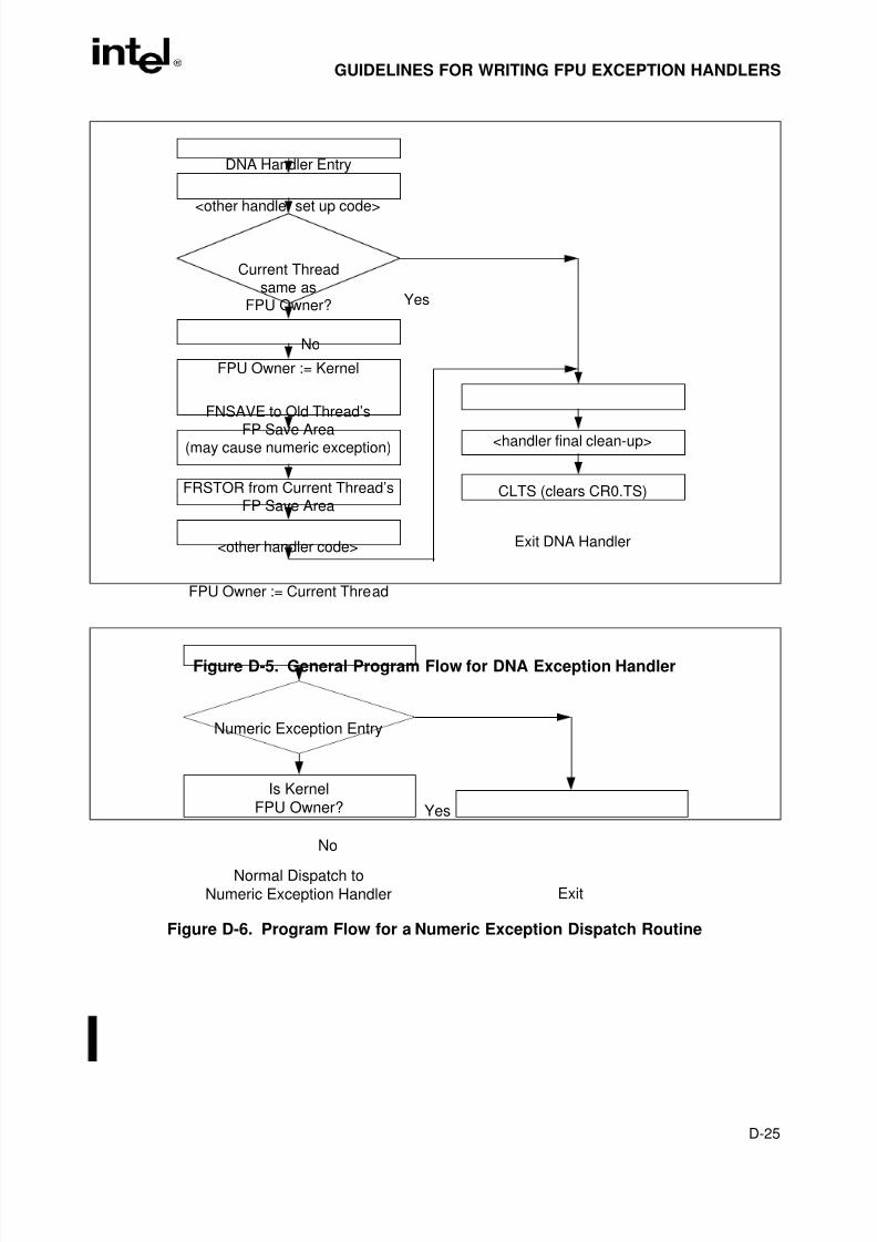
8/3/2019 Intel Architecture Software Developer's Manual, Volume 1: Basic Architecture
http://slidepdf.com/reader/full/intel-architecture-software-developers-manual-volume-1-basic-architecture 269/283
D-25
GUIDELINES FOR WRITING FPU EXCEPTION HANDLERS
Figure D-5. General Program Flow for DNA Exception Handler
Figure D-6. Program Flow for a Numeric Exception Dispatch Routine
DNA Handler Entry
Current Thread
same asFPU Owner?
FPU Owner := Kernel
FNSAVE to Old Thread’s
FP Save Area(may cause numeric exception)
<other handler set up code>
<other handler code>
FPU Owner := Current Thread
FRSTOR from Current Thread’s
FP Save AreaCLTS (clears CR0.TS)
Exit DNA Handler
No
Yes
<handler final clean-up>
Numeric Exception Entry
Is Kernel
FPU Owner?
Normal Dispatch to
Numeric Exception Handler Exit
No
Yes
8/3/2019 Intel Architecture Software Developer's Manual, Volume 1: Basic Architecture
http://slidepdf.com/reader/full/intel-architecture-software-developers-manual-volume-1-basic-architecture 270/283
D-26
GUIDELINES FOR WRITING FPU EXCEPTION HANDLERS
When the FNSAVE starts, it will trigger an interrupt via FERR# because of the pending numericexception. After some system dependent delay, the numeric exception handler is entered. It maybe entered before the FNSAVE starts to execute, or it may be entered shortly after execution of the FNSAVE. Since the FPU Owner is the kernel, the numeric exception handler simply exits,
discarding the exception. The DNA handler resumes execution, completing the FNSAVE of theold floating point context of thread A and the FRSTOR of the floating point context for thread B.
Thread A eventually gets an opportunity to handle the exception that was discarded during thetask switch. After some time, thread B is suspended, and thread A resumes execution. Whenthread A starts to execute an floating point instruction, once again the DNA exception handleris entered. B’s FPU state is Finessed, and A’s FPU state is Frustrate. Note that in restoring theFPU state from A’s save area, the pending numeric exception flags are reloaded in to the floatingpoint status word. Now when the DNA exception handler returns, thread A resumes executionof the faulting floating point instruction just long enough to immediately generate a numericexception, which now gets handled in the normal way. The net result is that the task switch and
resulting FPU state swap via the DNA exception handler causes an extra numeric exceptionwhich can be safely discarded.
D.3.6.4. INTERRUPT ROUTING FROM THE KERNEL
In MS-DOS, an application that wishes to handle numeric exceptions hooks interrupt 16 byplacing its handler address in the interrupt vector table, and exiting via a jump to the previousinterrupt 16 handler. Protected mode systems that run MS-DOS programs under a subsystem canemulate this exception delivery mechanism. For example, assume a protected mode O.S. thatruns with CR.NE = 1, and that runs MS-DOS programs in a virtual machine subsystem. The
MS-DOS program is set up in a virtual machine that provides a virtualized interrupt table. TheMS-DOS application hooks interrupt 16 in the virtual machine in the normal way. A numericexception will trap to the kernel via the real INT 16 residing in the kernel at ring 0. The INT 16handler in the kernel then locates the correct MS-DOS virtual machine, and reflects the interruptto the virtual machine monitor. The virtual machine monitor then emulates an interrupt by
jumping through the address in the virtualized interrupt table, eventually reaching the applica-tion’s numeric exception handler.
D.4. DIFFERENCES FOR HANDLERS USING NATIVE MODE
The 8087 has a pin INT which it asserts when an unmasked exception occurs. But there is nointerrupt input pin in the 8086 or 8088 dedicated to its attachment, nor an interrupt vectornumber in the 8086 or 8088 specific for an FPU error assertion. But beginning with the Intel 286and Intel 287 hardware connections were dedicated to support the FPU exception, and interruptvector 16 assigned to it.
8/3/2019 Intel Architecture Software Developer's Manual, Volume 1: Basic Architecture
http://slidepdf.com/reader/full/intel-architecture-software-developers-manual-volume-1-basic-architecture 271/283
D-27
GUIDELINES FOR WRITING FPU EXCEPTION HANDLERS
D.4.1. Origin With the Intel 286 and Intel 287, and Intel386™ andIntel 387 Processors
The Intel 286 and Intel 287, and Intel386 and Intel 387 processor/coprocessor pairs are each
provided with ERROR# pins that are recommended to be connected between the processor andFPU. If this is done, when an unmasked FPU exception occurs, the FPU records the exception,and asserts its ERROR# pin. The processor recognizes this active condition of the ERROR#status line immediately before execution of the next WAIT or FPU instruction (except for theno-wait type) in its instruction stream, and branches to the routine at interrupt vector 16. Thusan FPU exception will be handled before any other FPU instruction (after the one causing theerror) is executed (except for no-wait instructions, which will be executed without triggering theFPU exception interrupt, but it will remain pending).
Using the dedicated interrupt 16 for FPU exception handling is referred to as the native mode.It is the simplest approach, and the one recommended most highly by Intel.
D.4.2. Changes with Intel486™, Pentium® and Pentium ProProcessors with CR0.NE=1
With these latest three generations of the Intel Architecture, more enhancements and speedupfeatures have been added to the corresponding FPUs. Also, the FPU is now built into the samechip as the processor, which allows further increases in the speed at which the FPU can operateas part of the integrated system. This also means that the native mode of FPU exceptionhandling, selected by setting bit NE of register CR0 to 1, is now entirely internal.
If an unmasked exception occurs during an FPU instruction, the FPU records the exceptioninternally, and triggers the exception handler through interrupt 16 immediately before executionof the next WAIT or FPU instruction (except for no-wait instructions, which will be executed asdescribed in Section D.4.1., “Origin With the Intel 286 and Intel 287, and Intel386™ and Intel387 Processors”).
An unmasked numerical exception causes the FERR# output to be activated even with NE=1,and at exactly the same point in the program flow as it would have been asserted if NE werezero. However, the system would not connect FERR# to a PIC to generate INTR when operatingin the native, internal mode. (If the hardware of a system has FERR# connected to trigger IRQ13in order to support MS-DOS, but an O/S using the native mode is actually running the system,
it is the O/S’s responsibility to make sure that IRQ13 is not enabled in the slave PIC.) With thisconfiguration a system is immune to the problem discussed in Section D.2.1.3., “No-Wait FPUInstructions Can Get FPU Interrupt in Window”, where for Intel486 and Pentium processors ano-wait FPU instruction can get an FPU exception.
8/3/2019 Intel Architecture Software Developer's Manual, Volume 1: Basic Architecture
http://slidepdf.com/reader/full/intel-architecture-software-developers-manual-volume-1-basic-architecture 272/283
D-28
GUIDELINES FOR WRITING FPU EXCEPTION HANDLERS
D.4.3. Considerations When FPU Shared Between Tasks UsingNative Mode
The protocols recommended in Section D.3.6., “Considerations When FPU Shared Between
Tasks”, for MS-DOS compatibility FPU exception handlers that are shared between tasks maybe used without change with the native mode. However, the protocols for a handler writtenspecifically for native mode can be simplified, because the problem of a spurious floating pointexception interrupt occurring while the kernel is executing cannot happen in native mode.
The problem as actually found in practical code in a MS-DOS compatibility system happenswhen the DNA handler uses FNSAVE to switch FPU contexts. If an FPU exception is active,then FNSAVE triggers FERR# briefly, which usually will cause the FPU exception handler tobe invoked inside the DNA handler. In native mode, neither FNSAVE nor any other no-waitinstructions can trigger interrupt 16. (As discussed above, FERR# gets asserted independent of the value of the NE bit, but when NE=1, the O/S should not enable its path through the PIC.)
Another possible (very rare) way a floating point exception interrupt could occur while thekernel is executing is by an FPU immediate exception case having its interrupt delayed by theexternal hardware until execution has switched to the kernel. This also cannot happen in nativemode because there is no delay through external hardware.
Thus the native mode FPU exception handler can omit the test to see if the kernel is the FPUowner, and the DNA handler for a native mode system can omit the step of setting the kernel asthe FPU owner at the handler’s beginning. Since however these simplifications are minor andsave little code, it would be a reasonable and conservative habit (as long as the MS-DOScompatibility mode is widely used) to include these steps in all systems.
Note that the special DP (Dual Processing) mode for Pentium Processors, and also the moregeneral Intel MultiProcessor Specification for systems with multiple Pentium or Pentium Proprocessors, support FPU exception handling only in the native mode. Intel does not recommendusing the MS-DOS compatibility mode for systems using more than one processor.

8/3/2019 Intel Architecture Software Developer's Manual, Volume 1: Basic Architecture
http://slidepdf.com/reader/full/intel-architecture-software-developers-manual-volume-1-basic-architecture 273/283
Index

8/3/2019 Intel Architecture Software Developer's Manual, Volume 1: Basic Architecture
http://slidepdf.com/reader/full/intel-architecture-software-developers-manual-volume-1-basic-architecture 274/283
8/3/2019 Intel Architecture Software Developer's Manual, Volume 1: Basic Architecture
http://slidepdf.com/reader/full/intel-architecture-software-developers-manual-volume-1-basic-architecture 275/283
INDEX-1
INDEX
Numerics16-bitaddress size . . . . . . . . . . . . . . . . . . . . . . . . .3-5operand size . . . . . . . . . . . . . . . . . . . . . . . . .3-5
32-bitaddress size . . . . . . . . . . . . . . . . . . . . . . . . .3-5operand size . . . . . . . . . . . . . . . . . . . . . . . . .3-5
AAAA instruction. . . . . . . . . . . . . . . . . . . . . . . . .6-24AAD instruction . . . . . . . . . . . . . . . . . . . . . . . .6-24AAM instruction . . . . . . . . . . . . . . . . . . . . . . . .6-24AAS instruction. . . . . . . . . . . . . . . . . . . . . . . . .6-24AC (alignment check) flag, EFLAGS
register . . . . . . . . . . . . . . . . . . . . . . .3-13Access rights, segment descriptor . . . . . . 4-8, 4-11ADC instruction . . . . . . . . . . . . . . . . . . . . . . . .6-22ADD instruction . . . . . . . . . . . . . . . . . . . . . . . .6-22Address size attribute
code segment . . . . . . . . . . . . . . . . . . . . . . .3-14description of . . . . . . . . . . . . . . . . . . . . . . .3-14of stack . . . . . . . . . . . . . . . . . . . . . . . . . . . . .4-3
Address sizes. . . . . . . . . . . . . . . . . . . . . . . . . . .3-5Addressing modes
assembler . . . . . . . . . . . . . . . . . . . . . . . . . . .5-9base . . . . . . . . . . . . . . . . . . . . . . . . . . . 5-8
,5-9
base plus displacement . . . . . . . . . . . . . . . .5-9base plus index plus displacement. . . . . . . .5-9base plus index time scale plus
displacement . . . . . . . . . . . . . . . . . . . . . .5-9displacement. . . . . . . . . . . . . . . . . . . . . . . . .5-8effective address. . . . . . . . . . . . . . . . . . . . . .5-8immediate operands . . . . . . . . . . . . . . . . . . .5-5index . . . . . . . . . . . . . . . . . . . . . . . . . . . . . . .5-8index times scale plus displacement . . . . . .5-9memory operands. . . . . . . . . . . . . . . . . . . . .5-6register operands . . . . . . . . . . . . . . . . . . . . .5-5scale factor . . . . . . . . . . . . . . . . . . . . . . . . . .5-8
specifying a segment selector . . . . . . . . . . .5-6specifying an offset. . . . . . . . . . . . . . . . . . . .5-7Addressing, segments . . . . . . . . . . . . . . . . . . . .1-7Advanced programmable interrupt controller
(see APIC)AF (adjust) flag, EFLAGS register . . . . . . . . . .3-11AH register . . . . . . . . . . . . . . . . . . . . . . . . . . . . .3-7Alignment
of words, doublewords, and quadwords . . . .5-1AND instruction . . . . . . . . . . . . . . . . . . . . . . . .6-25APIC, presence of . . . . . . . . . . . . . . . . . . . . . .10-1Arctangent, FPU operation. . . . . . . . . . . . . . . .7-37Arithmetic instructions, FPU. . . . . . . . . . . . . . .7-43
Assembler, addressing modes. . . . . . . . . . . . . .5-9AX register . . . . . . . . . . . . . . . . . . . . . . . . . . . . .3-7
BB (default size) flag, segmentdescriptor . . . . . . . . . . . . . . . . .3-14, 4-3
Base (operand addressing) . . . . . . . . . . . .5-8, 5-9Basic execution environment . . . . . . . . . . . . . . 3-2B-bit, FPU status word . . . . . . . . . . . . . . . . . . 7-15BCD . . . . . . . . . . . . . . . . . . . . . . . . . . . . . . . . . 5-4BCD integers . . . . . . . . . . . . . . . . . . . . . . . . . . 5-4
FPU encoding . . . . . . . . . . . . . . . . . .7-28, 7-29packed. . . . . . . . . . . . . . . . . . . . . . . . .5-4, 6-24relationship to status flags. . . . . . . . . . . . . 3-12unpacked. . . . . . . . . . . . . . . . . . . . . . .5-4, 6-24
BH register . . . . . . . . . . . . . . . . . . . . . . . . . . . . 3-7
Bias valuenumeric overflow . . . . . . . . . . . . . . . . . . . . 7-51numeric underflow. . . . . . . . . . . . . . . . . . . 7-52
Biased exponent. . . . . . . . . . . . . . . . . . . . . . . . 7-5Binary numbers . . . . . . . . . . . . . . . . . . . . . . . . 1-6Binary-coded decimal (see BCD)Bit fields . . . . . . . . . . . . . . . . . . . . . . . . . . . . . . 5-4Bit order . . . . . . . . . . . . . . . . . . . . . . . . . . . . . . 1-5BOUND instruction . . . . . . . . . . . . 4-15, 6-34, 6-39BOUND range exceeded exception (#BR) . . . 4-15BP register . . . . . . . . . . . . . . . . . . . . . . . . . . . . 3-7Branch prediction . . . . . . . . . . . . . . . . . . . . . . . 2-7Branching, on FPU condition codes . . . .7-15, 7-36
BSF instruction . . . . . . . . . . . . . . . . . . . . . . . . 6-29BSR instruction. . . . . . . . . . . . . . . . . . . . . . . . 6-29BSWAP instruction . . . . . . . . . . . . . . . . . .6-2, 6-17BT instruction . . . . . . . . . . . . . . . . 3-10, 3-12, 6-29BTC instruction . . . . . . . . . . . . . . . 3-10, 3-12, 6-29BTR instruction . . . . . . . . . . . . . . . 3-10, 3-12, 6-29BTS instruction . . . . . . . . . . . . . . . 3-10, 3-12, 6-29Bus interface unit . . . . . . . . . . . . . . . . . . . . . . . 2-8BX register . . . . . . . . . . . . . . . . . . . . . . . . . . . . 3-7Byte . . . . . . . . . . . . . . . . . . . . . . . . . . . . . . . . . 5-1Byte order . . . . . . . . . . . . . . . . . . . . . . . . . . . . . 1-5
CC1 flag, FPU status word . . 7-13, 7-48, 7-51, 7-53C2 flag, FPU status word . . . . . . . . . . . . . . . . 7-13Call gate . . . . . . . . . . . . . . . . . . . . . . . . . . . . . . 4-7CALL instruction . . . . . . 3-14, 4-4, 4-8, 6-31, 6-39Calls (see Procedure calls)CBW instruction . . . . . . . . . . . . . . . . . . . . . . . 6-21CDQ instruction . . . . . . . . . . . . . . . . . . . . . . . 6-22CF (carry) flag, EFLAGS register . . . . . . . . . . 3-11CH register . . . . . . . . . . . . . . . . . . . . . . . . . . . . 3-7CLC instruction. . . . . . . . . . . . . . . . . . . .3-12, 6-37CLD instruction. . . . . . . . . . . . . . . . . . . .3-12, 6-37CLI instruction. . . . . . . . . . . . . . . . . . . . . .6-38, 9-4
CMC instruction . . . . . . . . . . . . . . . . . . .3-12, 6-37CMOVcc instructions . . . . . . . . . . . . . . . .6-1, 6-16
8/3/2019 Intel Architecture Software Developer's Manual, Volume 1: Basic Architecture
http://slidepdf.com/reader/full/intel-architecture-software-developers-manual-volume-1-basic-architecture 276/283
INDEX
INDEX-2
CMP instruction . . . . . . . . . . . . . . . . . . . . . . . .6-23CMPS instruction . . . . . . . . . . . . . . . . . . 3-12, 6-35CMPXCHG instruction . . . . . . . . . . . . . . . 6-2, 6-18CMPXCHG8B instruction. . . . . . . . 6-2, 6-18, 10-1Code segment . . . . . . . . . . . . . . . . . . . . . . . . . .3-9
Comparecompare and exchange . . . . . . . . . . . . . . .6-18integers . . . . . . . . . . . . . . . . . . . . . . . . . . . .6-23real numbers, FPU . . . . . . . . . . . . . . . . . . .7-35strings. . . . . . . . . . . . . . . . . . . . . . . . . . . . .6-35
Compatibilitysoftware . . . . . . . . . . . . . . . . . . . . . . . . . . . .1-5
Condition code flags, FPU status wordbranching on. . . . . . . . . . . . . . . . . . . . . . . .7-15conditional moves on . . . . . . . . . . . . . . . . .7-15description of . . . . . . . . . . . . . . . . . . . . . . .7-12interpretation of. . . . . . . . . . . . . . . . . . . . . .7-14use of . . . . . . . . . . . . . . . . . . . . . . . . . . . . .7-35
Conditional moves, on FPU condition codes . .7-15Constants (floating point)
descriptions of. . . . . . . . . . . . . . . . . . . . . . .7-33Cosine, FPU operation. . . . . . . . . . . . . . . . . . .7-37CPUID instruction. . . . . . . . . 6-2, 6-40, 10-1, 10-3CS register . . . . . . . . . . . . . . . . . . . . . . . . . 3-7, 3-9CTI instruction . . . . . . . . . . . . . . . . . . . . . . . . .6-37Current privilege level (see CPL)Current stack . . . . . . . . . . . . . . . . . . . . . . . 4-2, 4-4CWD instruction . . . . . . . . . . . . . . . . . . . . . . . .6-22CWDE instruction. . . . . . . . . . . . . . . . . . . . . . .6-21CX register . . . . . . . . . . . . . . . . . . . . . . . . . . . . .3-7
DDAA instruction . . . . . . . . . . . . . . . . . . . . . . . .6-24DAS instruction . . . . . . . . . . . . . . . . . . . . . . . .6-24Data pointer, FPU . . . . . . . . . . . . . . . . . . . . . .7-21Data segment. . . . . . . . . . . . . . . . . . . . . . . . . . .3-9Data types
alignment of words, doublewords, andquadwords. . . . . . . . . . . . . . . . . . . . . . . .5-1
BCD integers . . . . . . . . . . . . . . . . . . . 5-4, 6-24bit fields. . . . . . . . . . . . . . . . . . . . . . . . . . . . .5-4byte. . . . . . . . . . . . . . . . . . . . . . . . . . . . . . . .5-1doubleword . . . . . . . . . . . . . . . . . . . . . . . . . .5-1
FPU BCD decimal. . . . . . . . . . . . . . . . . . . .7-28FPU integer. . . . . . . . . . . . . . . . . . . . . . . . .7-27FPU real number . . . . . . . . . . . . . . . . . . . .7-25fundamental data types . . . . . . . . . . . . . . . .5-1integers . . . . . . . . . . . . . . . . . . . 5-2, 6-22, 6-23packed bytes. . . . . . . . . . . . . . . . . . . . . . . . .8-2packed doublewords. . . . . . . . . . . . . . . . . . .8-2packed words . . . . . . . . . . . . . . . . . . . . . . . .8-2pointers . . . . . . . . . . . . . . . . . . . . . . . . . . . . .5-4quadword . . . . . . . . . . . . . . . . . . . . . . . 5-1, 8-2strings. . . . . . . . . . . . . . . . . . . . . . . . . . . . . .5-4unsigned integers . . . . . . . . . . . 5-4, 6-22, 6-23word . . . . . . . . . . . . . . . . . . . . . . . . . . . . . . .5-1
DE (denormal operand exception) flag,FPU status word. . . . . . . . . . .7-14, 7-50
DEC instruction. . . . . . . . . . . . . . . . . . . . . . . . 6-22Decimal integers, FPU
description of. . . . . . . . . . . . . . . . . . . . . . . 7-28
encodings . . . . . . . . . . . . . . . . . . . . . . . . . 7-29Denormal number (see Denormalized finite
number)Denormal operand exception (#D) . . . . . . . . . 7-50Denormalization process . . . . . . . . . . . . . . . . . 7-7Denormalized finite number . . . . . . . . . . .7-6, 7-25DF (direction) flag, EFLAGS register . . . . . . . 3-12DH register . . . . . . . . . . . . . . . . . . . . . . . . . . . . 3-7DI register . . . . . . . . . . . . . . . . . . . . . . . . . . . . . 3-7Dispatch/execute unit . . . . . . . . . . . . . . . . . . . 2-11Displacement (operand addressing). . . . . .5-8, 5-9DIV instruction . . . . . . . . . . . . . . . . . . . . . . . . 6-23Division-by-zero exception (#Z) . . . . . . . . . . . 7-49
Double-extended-precision, IEEE floating-pointformat . . . . . . . . . . . . . . . . . . . . . . . 7-25
Double-precision, IEEE floating-pointformat . . . . . . . . . . . . . . . . . . . . . . . 7-25
Double-real floating-point format . . . . . . . . . . 7-25Doubleword . . . . . . . . . . . . . . . . . . . . . . . . . . . 5-1DS register . . . . . . . . . . . . . . . . . . . . . . . . .3-7, 3-9DX register . . . . . . . . . . . . . . . . . . . . . . . . . . . . 3-7Dynamic data flow analysis . . . . . . . . . . . . . . . 2-7Dynamic execution . . . . . . . . . . . . . . . . . . . . . . 2-7
E
EAX register . . . . . . . . . . . . . . . . . . . . . . . . . . . 3-5EBP register . . . . . . . . . . . . . . . . . . . . 3-5, 4-4, 4-6EBX register . . . . . . . . . . . . . . . . . . . . . . . . . . . 3-5ECX register . . . . . . . . . . . . . . . . . . . . . . . . . . . 3-5EDI register. . . . . . . . . . . . . . . . . . . . . . . . . . . . 3-5EDX register . . . . . . . . . . . . . . . . . . . . . . . . . . . 3-5Effective address . . . . . . . . . . . . . . . . . . . . . . . 5-8EFLAGS Condition Codes . . . . . . . . . . . . . . . . B-1EFLAGS register . . . . . . . . . . . . . . . . . . . . . . 3-10
restoring from procedure stack . . . . . . . . . . 4-7saving on a procedure call . . . . . . . . . . . . . 4-7status flags . . . . . . . . . . . . . . . 7-15, 7-16, 7-35
EIP register. . . . . . . . . . . . . . . . . . . . . . . .3-8, 3-14
EMMS instruction . . . . . . . . . . . . . . . . . . .8-9, 8-11ENTER instruction . . . . . . . . . . . . . . . . .4-16, 6-36ES register . . . . . . . . . . . . . . . . . . . . . . . . .3-7, 3-9ES (exception summary) flag,
FPU status word. . . . . . . . . . . . . . . 7-55ESC instructions, FPU . . . . . . . . . . . . . . . . . . 7-30ESI register. . . . . . . . . . . . . . . . . . . . . . . . . . . . 3-5ESP register . . . . . . . . . . . . . . . . 3-5, 4-1, 4-3, 4-4Exception flags, FPU status word. . . . . . . . . . 7-14Exception handler . . . . . . . . . . . . . . . . . . . . . . 4-10Exception priority, FPU exceptions. . . . . . . . . 7-53Exception-flag masks, FPU control word . . . . 7-17Exceptions
8/3/2019 Intel Architecture Software Developer's Manual, Volume 1: Basic Architecture
http://slidepdf.com/reader/full/intel-architecture-software-developers-manual-volume-1-basic-architecture 277/283
INDEX-3
INDEX
BOUND range exceeded (#BR) . . . . . . . . .4-15description of . . . . . . . . . . . . . . . . . . . . . . .4-10implicit call to handler . . . . . . . . . . . . . . . . . .4-1in real-address mode . . . . . . . . . . . . . . . . .4-15notation . . . . . . . . . . . . . . . . . . . . . . . . . . . . .1-7
overflow exception (#OF) . . . . . . . . . . . . . .4-15summary of . . . . . . . . . . . . . . . . . . . . . . . . .4-12vector . . . . . . . . . . . . . . . . . . . . . . . . . . . . .4-11
Exponentfloating-point number . . . . . . . . . . . . . . . . . .7-3
Exponential, FPU operation . . . . . . . . . . . . . . .7-38Extended real
encodings, unsupported . . . . . . . . . . . . . . .7-28floating-point format . . . . . . . . . . . . . . . . . .7-25
FF2XM1 instruction . . . . . . . . . . . . . . . . . . . . . .7-38
FABS instruction . . . . . . . . . . . . . . . . . . . . . . .7-33FADD instruction . . . . . . . . . . . . . . . . . . . . . . .7-33FADDP instruction . . . . . . . . . . . . . . . . . . . . . .7-33Far call
description of . . . . . . . . . . . . . . . . . . . . . . . .4-4operation. . . . . . . . . . . . . . . . . . . . . . . . . . . .4-6
Far pointer16-bit addressing . . . . . . . . . . . . . . . . . . . . .3-532-bit addressing . . . . . . . . . . . . . . . . . . . . .3-5description of . . . . . . . . . . . . . . . . . . . . 3-3, 5-4
FBSTP instruction . . . . . . . . . . . . . . . . . . . . . .7-32FCHS instruction . . . . . . . . . . . . . . . . . . . . . . .7-33FCLEX/FNCLEX instructions . . . . . . . . . . . . . .7-15
FCMOVcc instructions . . . . . . . . . . 6-1, 7-16, 7-32FCOM instruction . . . . . . . . . . . . . . . . . . 7-15, 7-34FCOMI instruction . . . . . . . . . . . . . 6-1, 7-16, 7-34FCOMIP instruction . . . . . . . . . . . . 6-1 , 7-16, 7-34FCOMP instruction. . . . . . . . . . . . . . . . . 7-15, 7-34FCOMPP instruction . . . . . . . . . . . . . . . 7-15, 7-34FCOS instruction . . . . . . . . . . . . . . . . . . 7-13, 7-37FDIV instruction . . . . . . . . . . . . . . . . . . . . . . . .7-33FDIVP instruction . . . . . . . . . . . . . . . . . . . . . . .7-33FDIVR instruction. . . . . . . . . . . . . . . . . . . . . . .7-33FDIVRP instruction. . . . . . . . . . . . . . . . . . . . . .7-33Feature determination, of processor . . . . . . . .10-1Fetch/decode unit. . . . . . . . . . . . . . . . . . . . . . .2-10
FIADD instruction. . . . . . . . . . . . . . . . . . . . . . .7-33FICOM instruction . . . . . . . . . . . . . . . . . 7-15, 7-34FICOMP instruction . . . . . . . . . . . . . . . . 7-15, 7-34FIDIV instruction. . . . . . . . . . . . . . . . . . . . . . . .7-33FIDIVR instruction . . . . . . . . . . . . . . . . . . . . . .7-33FILD instruction . . . . . . . . . . . . . . . . . . . . . . . .7-31FIMUL instruction . . . . . . . . . . . . . . . . . . . . . . .7-33FINIT/FNINIT instructions . 7-15, 7-16, 7-20, 7-40FIST instruction . . . . . . . . . . . . . . . . . . . . . . . .7-31FISTP instruction . . . . . . . . . . . . . . . . . . . . . . .7-32FISUB instruction . . . . . . . . . . . . . . . . . . . . . . .7-33FISUBR instruction. . . . . . . . . . . . . . . . . . . . . .7-33Flat memory model . . . . . . . . . . . . . . . . . . 3-3, 3-8
FLD instruction. . . . . . . . . . . . . . . . . . . . . . . . .7-31
FLD1 instruction . . . . . . . . . . . . . . . . . . . . . . . 7-33FLDCW instruction . . . . . . . . . . . . . . . . .7-16, 7-40FLDENV instruction . . . . . . 7-15, 7-20, 7-24, 7-40FLDL2E instruction. . . . . . . . . . . . . . . . . . . . . 7-33FLDL2T instruction . . . . . . . . . . . . . . . . . . . . . 7-33
FLDLG2 instruction. . . . . . . . . . . . . . . . . . . . . 7-33FLDLN2 instruction. . . . . . . . . . . . . . . . . . . . . 7-33FLDPI instruction . . . . . . . . . . . . . . . . . . . . . . 7-33FLDSW instruction . . . . . . . . . . . . . . . . . . . . . 7-40FLDZ instruction . . . . . . . . . . . . . . . . . . . . . . . 7-33Floating-point data types . . . . . . . . . . . . . . . . 7-24Floating-point exceptions
automatic handling . . . . . . . . . . . . . . . . . . 7-43denormal operand exception. . . . . . . . . . . 7-50division-by-zero. . . . . . . . . . . . . . . . . . . . . 7-49exception conditions . . . . . . . . . . . . . . . . . 7-47exception priority. . . . . . . . . . . . . . . . . . . . 7-53guidelines for writing exception handlers . . D-1
inexact-result (precision) . . . . . . . . . . . . . . 7-53invalid arithmetic operand . . . . . . . . .7-47, 7-48MS-DOS compatibility mode . . . . . . . . . . . . D-1numeric overflow . . . . . . . . . . . . . . . . . . . . 7-50numeric underflow. . . . . . . . . . . . . . . . . . . 7-52software handling . . . . . . . . . . . . . . . . . . . 7-45stack overflow . . . . . . . . . . . . . . . . . .7-13, 7-47stack underflow . . . . . . . . . . . . 7-13, 7-47, 7-48summary of . . . . . . . . . . . . . . . . . . . . . . . . 7-42synchronization . . . . . . . . . . . . . . . . . . . . . 7-54
Floating-point formatbiased exponent . . . . . . . . . . . . . . . . . . . . . 7-5description of. . . . . . . . . . . . . . . . . . . . . . . 7-24
exponent . . . . . . . . . . . . . . . . . . . . . . . . . . . 7-3fraction . . . . . . . . . . . . . . . . . . . . . . . . . . . . 7-3real number system. . . . . . . . . . . . . . . . . . . 7-2real numbers . . . . . . . . . . . . . . . . . . . . . . . 7-25sign . . . . . . . . . . . . . . . . . . . . . . . . . . . . . . . 7-3significand . . . . . . . . . . . . . . . . . . . . . . . . . . 7-3
FMUL instruction . . . . . . . . . . . . . . . . . . . . . . 7-33FMULP instruction . . . . . . . . . . . . . . . . . . . . . 7-33FNOP instruction . . . . . . . . . . . . . . . . . . . . . . 7-39FPATAN instruction . . . . . . . . . . . . . . . . . . . . 7-37FPREM instruction . . . . . . . . . . . . 7-13, 7-33, 7-37FPREM1 instruction . . . . . . . . . . . 7-13, 7-33, 7-37FPTAN instruction . . . . . . . . . . . . . . . . . . . . . 7-13
FPUarchitecture . . . . . . . . . . . . . . . . . . . . . . . . . 7-8compatibility with Intel Architecture FPUs
and math coprocessors . . . . . . . . . . . . . 7-1floating-point format . . . . . . . . . . . . . . .7-2, 7-3IEEE standards . . . . . . . . . . . . . . . . . . . . . . 7-1presence of . . . . . . . . . . . . . . . . . . . . . . . . 10-1transcendental instruction accuracy . . . . . 7-39
FPU control worddescription of. . . . . . . . . . . . . . . . . . . . . . . 7-16exception-flag masks . . . . . . . . . . . . . . . . 7-17PC field . . . . . . . . . . . . . . . . . . . . . . . . . . . 7-17RC field . . . . . . . . . . . . . . . . . . . . . . . . . . . 7-18
FPU data pointer . . . . . . . . . . . . . . . . . . . . . . 7-21
8/3/2019 Intel Architecture Software Developer's Manual, Volume 1: Basic Architecture
http://slidepdf.com/reader/full/intel-architecture-software-developers-manual-volume-1-basic-architecture 278/283
INDEX
INDEX-4
FPU data registers . . . . . . . . . . . . . . . . . . . . . . .7-9FPU instruction pointer. . . . . . . . . . . . . . . . . . .7-21FPU instructions
arithmetic vs. non-arithmetic instructions . .7-43instruction set . . . . . . . . . . . . . . . . . . . . . . .7-29
operands. . . . . . . . . . . . . . . . . . . . . . . . . . .7-31overview . . . . . . . . . . . . . . . . . . . . . . . . . . .7-29unsupported . . . . . . . . . . . . . . . . . . . . . . . .7-41
FPU integerdescription of . . . . . . . . . . . . . . . . . . . . . . .7-27encodings . . . . . . . . . . . . . . . . . . . . . . . . . .7-27
FPU last opcode. . . . . . . . . . . . . . . . . . . . . . . .7-21FPU register stack
description of . . . . . . . . . . . . . . . . . . . . . . . .7-9parameter passing . . . . . . . . . . . . . . . . . . .7-11
FPU stateimage . . . . . . . . . . . . . . . . . . . . . . . . 7-22, 7-23saving . . . . . . . . . . . . . . . . . . . . . . . . . . . . .7-21
FPU status wordcondition code flags . . . . . . . . . . . . . . . . . .7-12DE flag . . . . . . . . . . . . . . . . . . . . . . . . . . . .7-50description of . . . . . . . . . . . . . . . . . . . . . . .7-12exception flags . . . . . . . . . . . . . . . . . . . . . .7-14OE flag . . . . . . . . . . . . . . . . . . . . . . . . . . . .7-50PE flag . . . . . . . . . . . . . . . . . . . . . . . . . . . .7-13TOP field. . . . . . . . . . . . . . . . . . . . . . . . . . . .7-9
FPU tag word . . . . . . . . . . . . . . . . . . . . . . . . . .7-20Fraction, floating-point number . . . . . . . . . . . . .7-3FRNDINT instruction . . . . . . . . . . . . . . . . . . . .7-33FRSTOR instruction. . . . . . 7-15, 7-20, 7-24, 7-40FS register . . . . . . . . . . . . . . . . . . . . . . . . . 3-7, 3-9
FSAVE/FNSAVE instructions. . . .7-12, 7-15, 7-20,7-21, 7-40
FSCALE instruction . . . . . . . . . . . . . . . . . . . . .7-39FSIN instruction . . . . . . . . . . . . . . . . . . . 7-13, 7-37FSINCOS instruction . . . . . . . . . . . . . . . 7-13, 7-37FSQRT instruction . . . . . . . . . . . . . . . . . . . . . .7-33FST instruction. . . . . . . . . . . . . . . . . . . . . . . . .7-31FSTCW/FNSTCW instructions. . . . . . . . 7-16, 7-40FSTENV/FNSTENV
instructions. . . . . 7-12, 7-20, 7-21, 7-40FSTP instruction. . . . . . . . . . . . . . . . . . . . . . . .7-32FSTSW/FNSTSW instructions . . . . . . . . 7-12, 7-40FSUB instruction . . . . . . . . . . . . . . . . . . . . . . .7-33
FSUBP instruction . . . . . . . . . . . . . . . . . . . . . .7-33FSUBR instruction . . . . . . . . . . . . . . . . . . . . . .7-33FSUBRP instruction . . . . . . . . . . . . . . . . . . . . .7-33FTST instruction. . . . . . . . . . . . . . . . . . . 7-15, 7-34FUCOM instruction. . . . . . . . . . . . . . . . . . . . . .7-34FUCOMI instruction . . . . . . . . . . . . 6-1, 7-16, 7-34FUCOMIP instruction . . . . . . . . . . . 6-1, 7-16, 7-34FUCOMP instruction . . . . . . . . . . . . . . . . . . . .7-34FUCOMPP instruction . . . . . . . . . . . . . . 7-15, 7-34FXAM instruction . . . . . . . . . . . . . . . . . . 7-13, 7-34FXCH instruction . . . . . . . . . . . . . . . . . . . . . . .7-32FXTRACT instruction . . . . . . . . . . . . . . . . . . . .7-33FYL2X instruction. . . . . . . . . . . . . . . . . . . . . . .7-38
FYL2XP1 instruction . . . . . . . . . . . . . . . . . . . .7-38
GGeneral-purpose registers . . . . . . . . . . . . . . . . 3-5
parameter passing . . . . . . . . . . . . . . . . . . . 4-6GS register . . . . . . . . . . . . . . . . . . . . . . . . .3-7, 3-9
HHexadecimal numbers . . . . . . . . . . . . . . . . . . . 1-6
IID (identification) flag, EFLAGS register. . . . . 3-13IDIV instruction . . . . . . . . . . . . . . . . . . . . . . . . 6-23IE (invalid operation exception) flag,
FPU status word. . . . . . . . . . .7-14, 7-48IEEE 754 and 854 standards for
floating-point arithmetic . . . . . . . . . . 7-1IF (interrupt enable) flag, EFLAGS
register . . . . . . . . . . . . . . 3-13, 4-11, 9-5Immediate operands. . . . . . . . . . . . . . . . . . . . . 5-5IMUL instruction . . . . . . . . . . . . . . . . . . . . . . . 6-23IN . . . . . . . . . . . . . . . . . . . . . . . . . . . . . . . . . . . 9-3IN instruction. . . . . . . . . . . . . . . . . . . 6-36, 9-3, 9-4INC instruction . . . . . . . . . . . . . . . . . . . . . . . . 6-22Indefinite
description of. . . . . . . . . . . . . . . . . . . . . . . . 7-8integer . . . . . . . . . . . . . . . . . . . . . . . . . . . . 7-27packed BCD decimal. . . . . . . . . . . . . . . . . 7-28real . . . . . . . . . . . . . . . . . . . . . . . . . . . . . . 7-26
Index (operand addressing) . . . . . . . . . . . .5-8, 5-9Inexact result, FPU. . . . . . . . . . . . . . . . . . . . . 7-19
Inexact-result (precision) exception (#P) . . . . 7-53Infinity control flag, FPU control word. . . . . . . 7-20Infinity, floating-point format . . . . . . . . . . . . . . . 7-8INIT pin. . . . . . . . . . . . . . . . . . . . . . . . . . . . . . 3-10Input/output (see I/O)INS instruction . . . . . . . . . . . . . . . . . 6-36, 9-3, 9-4Instruction decoder. . . . . . . . . . . . . . . . . . . . . 2-10Instruction operands . . . . . . . . . . . . . . . . . . . . . 1-6Instruction pointer (EIP register). . . . . . . . . . . 3-14Instruction pointer, FPU . . . . . . . . . . . . . . . . . 7-21Instruction pool (reorder buffer) . . . . . . . . . . . 2-10Instruction prefixes (see Prefixes)Instruction set
binary arithmetic instructions. . . . . . . . . . . 6-22bit scan instructions. . . . . . . . . . . . . . . . . . 6-29bit test and modify instructions . . . . . . . . . 6-29byte-set-on-condition instructions . . . . . . . 6-29control transfer instructions. . . . . . . . . . . . 6-30data movement instructions . . . . . . . . . . . 6-16decimal arithmetic instructions . . . . . . . . . 6-23EFLAGS instructions. . . . . . . . . . . . . . . . . 6-37floating-point instructions . . . . . . . . . .6-9 , 6-11integer instructions . . . . . . . . . . . . . . . . . . . 6-3I/O instructions . . . . . . . . . . . . . . . . . . . . . 6-36lists of . . . . . . . . . . . . . . . . . . . . . . . . . . . . . 6-2logical instructions. . . . . . . . . . . . . . . . . . . 6-25
MMX instructions. . . . . . . . . . . . . . . . . . . . . 8-4
8/3/2019 Intel Architecture Software Developer's Manual, Volume 1: Basic Architecture
http://slidepdf.com/reader/full/intel-architecture-software-developers-manual-volume-1-basic-architecture 279/283
INDEX-5
INDEX
processor identification instruction . . . . . . .6-40repeating string operations . . . . . . . . . . . . .6-35rotate instructions . . . . . . . . . . . . . . . . . . . .6-27segment register instructions . . . . . . . . . . .6-38shift instructions . . . . . . . . . . . . . . . . . . . . .6-25
software interrupt instructions. . . . . . . . . . .6-34string operation instructions . . . . . . . . . . . .6-34summary . . . . . . . . . . . . . . . . . . . . . . . . . . . .6-1system instructions . . . . . . . . . . . . . . . . . . .6-15test instruction. . . . . . . . . . . . . . . . . . . . . . .6-30type conversion instructions . . . . . . . . . . . .6-21
INT instruction . . . . . . . . . . . . . . . . . . . . 4-15, 6-39Integers . . . . . . . . . . . . . . . . . . . . . 5-2, 6-22, 6-23Integer, FPU data type
description of . . . . . . . . . . . . . . . . . . . . . . .7-27indefinite . . . . . . . . . . . . . . . . . . . . . . . . . . .7-27
Inter-privilege level calldescription of . . . . . . . . . . . . . . . . . . . . . . . .4-7
operation. . . . . . . . . . . . . . . . . . . . . . . . . . . .4-9Inter-privilege level return
description of . . . . . . . . . . . . . . . . . . . . . . . .4-7operation. . . . . . . . . . . . . . . . . . . . . . . . . . . .4-9
Interrupt gate . . . . . . . . . . . . . . . . . . . . . . . . . .4-11Interrupt handler. . . . . . . . . . . . . . . . . . . . . . . .4-10Interrupt vector. . . . . . . . . . . . . . . . . . . . . . . . .4-11Interrupts
description of . . . . . . . . . . . . . . . . . . . . . . .4-10implicit call to an interrupt handler
procedure . . . . . . . . . . . . . . . . . . . . . . .4-11implicit call to an interrupt handler task. . . .4-14in real-address mode . . . . . . . . . . . . . . . . .4-15
maskable . . . . . . . . . . . . . . . . . . . . . . . . . .4-11summary of . . . . . . . . . . . . . . . . . . . . . . . . .4-12user-defined . . . . . . . . . . . . . . . . . . . . . . . .4-11vector . . . . . . . . . . . . . . . . . . . . . . . . . . . . .4-11
INTn instruction . . . . . . . . . . . . . . . . . . . . . . . .6-34INTO instruction . . . . . . . . . . . . . . 4-15, 6-34, 6-39Invalid arithmetic operand exception (#IA), FPU
description of . . . . . . . . . . . . . . . . . . . . . . .7-48masked response to . . . . . . . . . . . . . . . . . .7-49
Invalid operation exception . . . . . . . . . . . . . . .7-47INVD instruction . . . . . . . . . . . . . . . . . . . . . . . . .6-2INVLPG instruction. . . . . . . . . . . . . . . . . . . . . . .6-2IOPL (I/O privilege level) field, EFLAGS
register . . . . . . . . . . . . . . . . . . . 3-13, 9-4IRET instruction . 3-14, 4-14, 4-15, 6-31, 6-39, 9-5I/O address space . . . . . . . . . . . . . . . . . . . . . . .9-2I/O instructions
overview of . . . . . . . . . . . . . . . . . . . . . 6-36, 9-3serialization. . . . . . . . . . . . . . . . . . . . . . . . . .9-6
I/O map base . . . . . . . . . . . . . . . . . . . . . . . . . . .9-5I/O permission bit map . . . . . . . . . . . . . . . . . . . .9-5I/O ports
addressing . . . . . . . . . . . . . . . . . . . . . . . . . .9-1defined . . . . . . . . . . . . . . . . . . . . . . . . . . . . .9-1hardware. . . . . . . . . . . . . . . . . . . . . . . . . . . .9-1memory-mapped I/O. . . . . . . . . . . . . . . . . . .9-2
ordering. . . . . . . . . . . . . . . . . . . . . . . . . . . . .9-6protected mode I/O . . . . . . . . . . . . . . . . . . . .9-4
I/O privilege level (see IOPL)I/O sensitive instructions. . . . . . . . . . . . . . . . . . 9-4
J
J-bit. . . . . . . . . . . . . . . . . . . . . . . . . . . . . . . . . . 7-3Jcc instructions . . . . . . . . . . . . . . . 3-12, 3-14, 6-32JMP instruction . . . . . . . . . . . . . . . 3-14, 6-30, 6-39
LL1 (level 1) cache . . . . . . . . . . . . . . . . . . . .2-6, 2-8L2 (level 2) cache . . . . . . . . . . . . . . . . . . . .2-6, 2-8LAHF instruction. . . . . . . . . . . . . . . . . . .3-10, 6-37Last instruction opcode, FPU . . . . . . . . . . . . . 7-21LDS instruction . . . . . . . . . . . . . . . . . . . . . . . . 6-39LEA instruction . . . . . . . . . . . . . . . . . . . . . . . . 6-39LEAVE instruction. . . . . . . . . . . . . 4-16, 4-21, 6-36
LES instruction . . . . . . . . . . . . . . . . . . . . . . . . 6-39LGS instruction. . . . . . . . . . . . . . . . . . . . . . . . 6-39Linear address . . . . . . . . . . . . . . . . . . . . . . . . . 3-3Linear address space
defined . . . . . . . . . . . . . . . . . . . . . . . . . . . . 3-3maximum size . . . . . . . . . . . . . . . . . . . . . . . 3-3
LOCK signal . . . . . . . . . . . . . . . . . . . . . . . . . . 6-17LODS instruction . . . . . . . . . . . . . . . . . .3-12, 6-35Log epsilon, FPU operation . . . . . . . . . . . . . . 7-38Log (base 2), FPU computation . . . . . . . . . . . 7-38Logical address . . . . . . . . . . . . . . . . . . . . . . . . 3-3LOOP instructions . . . . . . . . . . . . . . . . . . . . . 6-33LOOPcc instructions. . . . . . . . . . . . . . . .3-12, 6-33
LSS instruction . . . . . . . . . . . . . . . . . . . . . . . . 6-39
MMaskable interrupts . . . . . . . . . . . . . . . . . . . . 4-11Masked responses
to denormal operand exception. . . . . . . . . 7-50to division-by-zero exception. . . . . . . . . . . 7-50to FPU stack overflow or underflow
exception . . . . . . . . . . . . . . . . . . . . . . . 7-48to inexact-result (precision) exception. . . . 7-53to invalid arithmetic operation . . . . . . . . . . 7-49to numeric overflow exception. . . . . . . . . . 7-51
to numeric underflow exception . . . . . . . . 7-52Masks, exception-flags, FPU control word . . . 7-17Memory
order buffer . . . . . . . . . . . . . . . . . . . . . . . . . 2-9organization. . . . . . . . . . . . . . . . . . . . . .3-2, 3-3subsystem . . . . . . . . . . . . . . . . . . . . . . . . . . 2-8
Memory interface unit . . . . . . . . . . . . . . . . . . . . 2-8Memory operands. . . . . . . . . . . . . . . . . . . . . . . 5-6Memory-mapped I/O. . . . . . . . . . . . . . . . . .9-1, 9-2MESI (modified, exclusive, shared, invalid) cache
protocol. . . . . . . . . . . . . . . . . . . . . . . 2-8Microarchitecture
detailed description . . . . . . . . . . . . . . . . . . . 2-8
overview . . . . . . . . . . . . . . . . . . . . . . . . . . . 2-5Micro-ops . . . . . . . . . . . . . . . . . . . . . . . . . . . . 2-10
8/3/2019 Intel Architecture Software Developer's Manual, Volume 1: Basic Architecture
http://slidepdf.com/reader/full/intel-architecture-software-developers-manual-volume-1-basic-architecture 280/283
INDEX
INDEX-6
MM0, MM1, MM2, MM3, MM4, MM5, MM6,MM7 registers . . . . . . . . . . . . . . . . . .8-2
MMX technologyarithmetic instructions. . . . . . . . . . . . . . . . . .8-8comparison instructions . . . . . . . . . . . . . . . .8-8
compatibility with FPU architecture. . . . . . .8-10conversion instructions . . . . . . . . . . . . . . . . .8-9CPUID instruction . . . . . . . . . . . . . . . . . . . .10-2data transfer instructions . . . . . . . . . . . . . . .8-6data types . . . . . . . . . . . . . . . . . . . . . . . . . . .8-2detecting MMX technology with CPUID
instruction . . . . . . . . . . . . . . . . . . . . . . .8-10detecting with CPUID instruction . . . . . . . .8-11effect of instruction prefixes on MMX
instructions . . . . . . . . . . . . . . . . . . . . . .8-10EMMS instruction . . . . . . . . . . . . . . . . . . . . .8-9exception handling in MMX code . . . . . . . .8-15instruction operands . . . . . . . . . . . . . . . . . . .8-6
instruction set . . . . . . . . . . . . . . . . . . . . 8-4, 8-6interfacing with MMX code . . . . . . . . . . . . .8-12introduction to . . . . . . . . . . . . . . . . . . . . . . . .8-1logical instructions . . . . . . . . . . . . . . . . . . . .8-9memory data formats . . . . . . . . . . . . . . . . . .8-4mixing MMX and floating-point
instructions . . . . . . . . . . . . . . . . . . . . . .8-13programming environment (overview) . . . . .8-1register data formats. . . . . . . . . . . . . . . . . . .8-4register mapping . . . . . . . . . . . . . . . . . . . . .8-15registers . . . . . . . . . . . . . . . . . . . . . . . . . . . .8-2saturation arithmetic . . . . . . . . . . . . . . . . . . .8-5shift instructions . . . . . . . . . . . . . . . . . . . . . .8-9
SIMD execution environment . . . . . . . . . . . .8-3support for, determing. . . . . . . . . . . . . . . . .10-2using MMX code in a multitasking
operating system environment . . . . . . .8-14using the EMMS instruction . . . . . . . . . . . .8-11wraparound mode. . . . . . . . . . . . . . . . . . . . .8-5
Modes, operating . . . . . . . . . . . . . . . . . . . . . . . .3-4MOV instruction . . . . . . . . . . . . . . . . . . . 6-16, 6-38MOVD instruction. . . . . . . . . . . . . . . . . . . . . . . .8-6MOVQ instruction. . . . . . . . . . . . . . . . . . . . . . . .8-6MOVS instruction . . . . . . . . . . . . . . . . . . 3-12, 6-35MOVSX instruction. . . . . . . . . . . . . . . . . . . . . .6-22MOVZX instruction . . . . . . . . . . . . . . . . . . . . . .6-22
MS-DOS compatibility mode . . . . . . . . . . . . . . D-1MTRRs (memory type range registers)
presence of . . . . . . . . . . . . . . . . . . . . . . . . .10-1MUL instruction . . . . . . . . . . . . . . . . . . . . . . . .6-23
NNaN
description of . . . . . . . . . . . . . . . . . . . . 7-5, 7-8encoding of . . . . . . . . . . . . . . . . . . . . . 7-6, 7-26operating on . . . . . . . . . . . . . . . . . . . . . . . .7-41SNaNs vs. QNaNs . . . . . . . . . . . . . . . . . . . .7-8
Near call
description of . . . . . . . . . . . . . . . . . . . . . . . .4-4operation. . . . . . . . . . . . . . . . . . . . . . . . . . . .4-5
Near pointerdescription of. . . . . . . . . . . . . . . . . . . . . . . . 5-4
Near returnoperation . . . . . . . . . . . . . . . . . . . . . . . . . . . 4-5
Near return operation . . . . . . . . . . . . . . . . . . . . 4-6
NEG instruction . . . . . . . . . . . . . . . . . . . . . . . 6-23Non-arithmetic instructions, FPU . . . . . . . . . . 7-43Non-number encodings, FPU. . . . . . . . . . . . . . 7-5Non-waiting instructions . . . . . . . . . . . . .7-40, 7-45NOP instruction . . . . . . . . . . . . . . . . . . . . . . . 6-40Normalized finite number . . . . . . . . . . . . . .7-4, 7-6NOT instruction. . . . . . . . . . . . . . . . . . . . . . . . 6-25Notation
bit and byte order . . . . . . . . . . . . . . . . . . . . 1-5exceptions. . . . . . . . . . . . . . . . . . . . . . . . . . 1-7hexadecimal and binary numbers . . . . . . . . 1-6instruction operands . . . . . . . . . . . . . . . . . . 1-6reserved bits . . . . . . . . . . . . . . . . . . . . . . . . 1-5
segmented addressing . . . . . . . . . . . . . . . . 1-7Notational conventions . . . . . . . . . . . . . . . . . . . 1-5NT (nested task) flag, EFLAGS register . . . . . 3-13Numeric overflow exception (#O) . . . . . .7-13, 7-50Numeric underflow exception (#U) . . . . .7-13, 7-52
OOE (numeric overflow exception) flag,
FPU status word. . . . . . . . . . .7-14, 7-51OF (overflow) flag, EFLAGS register . . .3-11, 4-15Offset (operand addressing). . . . . . . . . . . . . . . 5-7Operand
FPU instructions . . . . . . . . . . . . . . . . . . . . 7-31instruction . . . . . . . . . . . . . . . . . . . . . . . . . . 1-6
Operand addressing, modes . . . . . . . . . . . . . . 5-5Operand sizes . . . . . . . . . . . . . . . . . . . . . . . . . 3-5Operand-size attribute
code segment . . . . . . . . . . . . . . . . . . . . . . 3-14description of. . . . . . . . . . . . . . . . . . . . . . . 3-14
Operating modes . . . . . . . . . . . . . . . . . . . . . . . 3-4OR instruction. . . . . . . . . . . . . . . . . . . . . . . . . 6-25Ordering I/O . . . . . . . . . . . . . . . . . . . . . . . . . . . 9-6OUT instruction. . . . . . . . . . . . . . . . . 6-36, 9-3, 9-4OUTS instruction . . . . . . . . . . . . . . . 6-36, 9-3, 9-4Overflow exception (#OF). . . . . . . . . . . . . . . . 4-15
Overflow, FPU exception (see Numeric overflowexception)
Overflow, FPU stack. . . . . . . . . . . . . . . .7-47, 7-48
PPacked BCD integers . . . . . . . . . . . . . . . . . . . . 5-4Packed bytes data type . . . . . . . . . . . . . . . . . . 8-2Packed decimal indefinite. . . . . . . . . . . . . . . . 7-28Packed doublewords data type . . . . . . . . . . . . 8-2Packed words data type . . . . . . . . . . . . . . . . . . 8-2Parameter passing
argument list . . . . . . . . . . . . . . . . . . . . . . . . 4-7
FPU register stack. . . . . . . . . . . . . . . . . . . 7-11on procedure stack . . . . . . . . . . . . . . . . . . . 4-6
8/3/2019 Intel Architecture Software Developer's Manual, Volume 1: Basic Architecture
http://slidepdf.com/reader/full/intel-architecture-software-developers-manual-volume-1-basic-architecture 281/283
INDEX-7
INDEX
on the procedure stack . . . . . . . . . . . . . . . . .4-6through general-purpose registers . . . . . . . .4-6
PC (precision) field, FPU control word. . . . . . .7-17PE (inexact result exception) flag, FPU status
word . . . . . . . . . . 7-13, 7-14, 7-19, 7-53
Pentium Pro processormicroarchitecture . . . . . . . . . . . . . . . . . 2-5, 2-8
PF (parity) flag, EFLAGS register . . . . . . . . . .3-11Physical address space . . . . . . . . . . . . . . . . . . .3-2Physical memory . . . . . . . . . . . . . . . . . . . . . . . .3-2Pi
description of FPU constant . . . . . . . . . . . .7-37Pointers . . . . . . . . . . . . . . . . . . . . . . . . . . . . . . .5-4POP instruction . . . . . . . . . . . 4-1, 4-3, 6-20, 6-38POPA instruction . . . . . . . . . . . . . . . . . . . 4-7, 6-20POPF instruction . . . . . . . . . . 3-10, 4-7, 6-37, 9-5POPFD instruction . . . . . . . . . . . . . 3-10, 4-7, 6-37Privilege levels
description of . . . . . . . . . . . . . . . . . . . . . . . .4-8inter-privilege level calls . . . . . . . . . . . . . . . .4-7stack switching . . . . . . . . . . . . . . . . . . . . . .4-11
Procedure callsdescription of . . . . . . . . . . . . . . . . . . . . . . . .4-4far call . . . . . . . . . . . . . . . . . . . . . . . . . . . . . .4-4for block-structured languages . . . . . . . . . .4-16inter-privilege level call . . . . . . . . . . . . . . . . .4-9linking . . . . . . . . . . . . . . . . . . . . . . . . . . . . . .4-3near call . . . . . . . . . . . . . . . . . . . . . . . . . . . .4-4overview . . . . . . . . . . . . . . . . . . . . . . . . . . . .4-1procedure stack . . . . . . . . . . . . . . . . . . . . . .4-1return instruction pointer (EIP register). . . . .4-4
saving procedure state information. . . . . . . .4-7stack switching . . . . . . . . . . . . . . . . . . . . . . .4-8to exception handler procedure . . . . . . . . .4-11to exception task. . . . . . . . . . . . . . . . . . . . .4-14to interrupt handler procedure . . . . . . . . . .4-11to interrupt task. . . . . . . . . . . . . . . . . . . . . .4-14to other privilege levels . . . . . . . . . . . . . . . . .4-7types of . . . . . . . . . . . . . . . . . . . . . . . . . . . . .4-1
Procedure stackaddress-size attribute . . . . . . . . . . . . . . . . . .4-3alignment of stack pointer. . . . . . . . . . . . . . .4-3current stack . . . . . . . . . . . . . . . . . . . . . 4-2, 4-4description of . . . . . . . . . . . . . . . . . . . . . . . .4-1
EIP register (return instruction pointer). . . . .4-4maximum size. . . . . . . . . . . . . . . . . . . . . . . .4-1number allowed . . . . . . . . . . . . . . . . . . . . . .4-1passing parameters on . . . . . . . . . . . . . . . . .4-6popping values from . . . . . . . . . . . . . . . . . . .4-1procedure linking information . . . . . . . . . . . .4-3pushing values on. . . . . . . . . . . . . . . . . . . . .4-1return instruction pointer . . . . . . . . . . . . . . . .4-4SS register . . . . . . . . . . . . . . . . . . . . . . . . . .4-1stack pointer . . . . . . . . . . . . . . . . . . . . . . . . .4-1stack segment. . . . . . . . . . . . . . . . . . . . . . . .4-1stack-frame base pointer, EBP register . . . .4-4switching. . . . . . . . . . . . . . . . . . . . . . . . . . . .4-8
top of stack . . . . . . . . . . . . . . . . . . . . . . . . . .4-1width . . . . . . . . . . . . . . . . . . . . . . . . . . . . . . .4-3
Processor identificationearlier Intel architecture processors . . . . . 10-3using CPUID instruction . . . . . . . . . . . . . . 10-1
Processor state information, saving on aprocedure call. . . . . . . . . . . . . . . . . . 4-7
Protected modedescription of. . . . . . . . . . . . . . . . . . . . . . . . 3-4I/O . . . . . . . . . . . . . . . . . . . . . . . . . . . . . . . . 9-4
Pseudo-denormal number . . . . . . . . . . . . . . . 7-29Pseudo-infinity . . . . . . . . . . . . . . . . . . . . . . . . 7-28Pseudo-NaN. . . . . . . . . . . . . . . . . . . . . . . . . . 7-28PUSH instruction . . . . . . . . . . 4-1, 4-3, 6-19, 6-38PUSHA instruction . . . . . . . . . . . . . . . . . .4-7, 6-19PUSHF instruction . . . . . . . . . . . . . 3-10, 4-7, 6-37PUSHFD instruction . . . . . . . . . . . . 3-10, 4-7, 6-37
Q
QNaNdescription of. . . . . . . . . . . . . . . . . . . . . . . . 7-8operating on . . . . . . . . . . . . . . . . . . . . . . . 7-41rules for generating . . . . . . . . . . . . . . . . . . 7-41
Quadword . . . . . . . . . . . . . . . . . . . . . . . . . .5-1, 8-2Quiet NaN (see QNaN)
RRC (rounding control) field,
FPU control word . . . . . . . . . . . . . . 7-18RCL instruction. . . . . . . . . . . . . . . . . . . . . . . . 6-28RCR instruction . . . . . . . . . . . . . . . . . . . . . . . 6-28
RDMSR instruction. . . . . . . . . . . . . . . . . .6-2, 10-1RDPMC instruction . . . . . . . . . . . . . . . . . . . . . . 6-1RDTSC instruction . . . . . . . . . . . . . . . . . .6-2, 10-1Real numbers
encoding . . . . . . . . . . . . . . . . . . . 7-5, 7-6, 7-26floating-point format . . . . . . . . . . . . . . . . . 7-25indefinite . . . . . . . . . . . . . . . . . . . . . . . . . . 7-26notation . . . . . . . . . . . . . . . . . . . . . . . . . . . . 7-5system. . . . . . . . . . . . . . . . . . . . . . . . . . . . . 7-2
Real-address mode . . . . . . . . . . . . . . . . . . . . . 3-4handling exceptions in. . . . . . . . . . . . . . . . 4-15handling interrupts in. . . . . . . . . . . . . . . . . 4-15
Register operands . . . . . . . . . . . . . . . . . . . . . . 5-5
Register stack, FPU . . . . . . . . . . . . . . . . . . . . . 7-9RegistersEFLAGS register. . . . . . . . . . . . . . . . . . . . 3-10EIP register . . . . . . . . . . . . . . . . . . . . . . . . 3-14general-purpose registers . . . . . . . . . . . . . . 3-5segment registers . . . . . . . . . . . . . . . . .3-5, 3-7
Related literature . . . . . . . . . . . . . . . . . . . . . . . 1-7REP/REPE/REPZ/REPNE/REPNZ
prefixes. . . . . . . . . . . . . . . . . . .6-35, 9-4Reserved bits . . . . . . . . . . . . . . . . . . . . . . . . . . 1-5RESET pin . . . . . . . . . . . . . . . . . . . . . . . . . . . 3-10RET instruction. . . . . . . . . . . 3-14, 4-4, 6-31, 6-39Retirement unit . . . . . . . . . . . . . . . . . . . . . . . . 2-12
Return instruction pointer . . . . . . . . . . . . . . . . . 4-4
8/3/2019 Intel Architecture Software Developer's Manual, Volume 1: Basic Architecture
http://slidepdf.com/reader/full/intel-architecture-software-developers-manual-volume-1-basic-architecture 282/283
INDEX
INDEX-8
Returns, from procedure callsexception handler, return from . . . . . . . . . .4-11far return . . . . . . . . . . . . . . . . . . . . . . . . . . . .4-6interrupt handler, return from . . . . . . . . . . .4-11
Returns, from procedures calls
inter-privilege level return . . . . . . . . . . . . . . .4-9near return . . . . . . . . . . . . . . . . . . . . . . . . . .4-5
RF (resume) flag, EFLAGS register . . . . . . . . .3-13ROL instruction . . . . . . . . . . . . . . . . . . . . . . . .6-28ROR instruction . . . . . . . . . . . . . . . . . . . . . . . .6-28Rounding
control, RC field of FPU control word . . . . .7-18modes, FPU . . . . . . . . . . . . . . . . . . . . . . . .7-18results, FPU . . . . . . . . . . . . . . . . . . . . . . . .7-19
RSM instruction . . . . . . . . . . . . . . . . . . . . . . . . .6-2
S
SAHF instruction . . . . . . . . . . . . . . . . . . 3-10, 6-37SAL instruction. . . . . . . . . . . . . . . . . . . . . . . . .6-25SAR instruction . . . . . . . . . . . . . . . . . . . . . . . .6-26Saturation arithmetic (MMX instructions) . . . . . .8-5Saving the FPU state . . . . . . . . . . . . . . . . . . . .7-21SBB instruction. . . . . . . . . . . . . . . . . . . . . . . . .6-22Scale (operand addressing) . . . . . . . . . . . . 5-8, 5-9Scale, FPU operation . . . . . . . . . . . . . . . . . . . .7-38Scaling bias value . . . . . . . . . . . . . . . . . 7-51, 7-52SCAS instruction . . . . . . . . . . . . . . . . . . 3-12, 6-35Segment registers
description of . . . . . . . . . . . . . . . . . . . . 3-5, 3-7Segment selector
description of . . . . . . . . . . . . . . . . . . . . 3-3, 3-7specifying . . . . . . . . . . . . . . . . . . . . . . . . . . .5-6
Segmented addressing . . . . . . . . . . . . . . . . . . .1-7Segmented memory model . . . . . . . . . . . . 3-3, 3-8Segments
defined . . . . . . . . . . . . . . . . . . . . . . . . . . . . .3-3maximum number. . . . . . . . . . . . . . . . . . . . .3-3
Serialization of I/O instructions. . . . . . . . . . . . . .9-6SETcc instructions . . . . . . . . . . . . . . . . . 3-12, 6-29SF (sign) flag, EFLAGS register. . . . . . . . . . . .3-11SF (stack fault) flag, FPU status word . . 7-15, 7-48SHL instruction. . . . . . . . . . . . . . . . . . . . . . . . .6-25SHLD instruction . . . . . . . . . . . . . . . . . . . . . . .6-27
SHR instruction . . . . . . . . . . . . . . . . . . . . . . . .6-25SHRD instruction . . . . . . . . . . . . . . . . . . . . . . .6-27SI register. . . . . . . . . . . . . . . . . . . . . . . . . . . . . .3-7Signaling NaN (see SNaN)Signed infinity. . . . . . . . . . . . . . . . . . . . . . . . . . .7-8Signed zero . . . . . . . . . . . . . . . . . . . . . . . . . . . .7-6Significand
of floating-point number . . . . . . . . . . . . . . . .7-3Sign, floating-point number . . . . . . . . . . . . . . . .7-3SIMD (single-instruction, multiple-data)
execution model. . . . . . . . . . . . . . . . .8-3Sine, FPU operation. . . . . . . . . . . . . . . . . . . . .7-37Single-precision, IEEE floating-point format. . .7-25
Single-real floating-point format . . . . . . . . . . . 7-25SNaN
description of. . . . . . . . . . . . . . . . . . . . . . . . 7-8operating on . . . . . . . . . . . . . . . . . . . . . . . 7-41typical uses of . . . . . . . . . . . . . . . . . . . . . . 7-41
SP register . . . . . . . . . . . . . . . . . . . . . . . . . . . . 3-7Speculative execution. . . . . . . . . . . . . . . . . . . . 2-6SS register . . . . . . . . . . . . . . . . . . . . . 3-7, 3-9, 4-1Stack alignment . . . . . . . . . . . . . . . . . . . . . . . . 4-3Stack fault, FPU . . . . . . . . . . . . . . . . . . . . . . . 7-15Stack overflow and underflow exceptions (#IS),
FPU . . . . . . . . . . . . . . . . . . . . . . . . 7-48Stack overflow exception, FPU. . . . . . . .7-13 , 7-47Stack pointer (ESP register) . . . . . . . . . . . . . . . 4-1Stack segment . . . . . . . . . . . . . . . . . . . . . . . . . 3-9Stack switching
on calls to interrupt and exceptionhandlers . . . . . . . . . . . . . . . . . . . . . . . . 4-11
on inter-privilege level calls . . . . . . . . .4-9, 4-14Stack underflow exception, FPU . . . . . .7-13, 7-47Stack (see Procedure stack)Stack-frame base pointer, EBP register . . . . . . 4-4Status flags, EFLAGS register . . 3-11, 7-15, 7-16,
7-35STC instruction. . . . . . . . . . . . . . . . . . . .3-12, 6-37STD instruction. . . . . . . . . . . . . . . . . . . .3-12, 6-37STI instruction. . . . . . . . . . . . . . . . . 6-37, 6-38, 9-4STOS instruction . . . . . . . . . . . . . . . . . .3-12, 6-35Strings . . . . . . . . . . . . . . . . . . . . . . . . . . . . . . . 5-4ST(0), top-of-stack register. . . . . . . . . . . . . . . 7-11SUB instruction. . . . . . . . . . . . . . . . . . . . . . . . 6-22
Superscaler . . . . . . . . . . . . . . . . . . . . . . . . . . . 2-6Synchronization, of floating-point exceptions . 7-54System flags, EFLAGS register . . . . . . . . . . . 3-13System management mode (SSM) . . . . . . . . . 3-4
TTangent, FPU operation . . . . . . . . . . . . . . . . . 7-37Task gate . . . . . . . . . . . . . . . . . . . . . . . . . . . . 4-14Task state segment (see TSS)Tasks
exception handler . . . . . . . . . . . . . . . . . . . 4-14interrupt handler . . . . . . . . . . . . . . . . . . . . 4-14
TEST instruction. . . . . . . . . . . . . . . . . . . . . . . 6-30TF (trap) flag, EFLAGS register . . . . . . . . . . . 3-13Tiny number . . . . . . . . . . . . . . . . . . . . . . . . . . . 7-7TOP (stack TOP) field, FPU status word . . . . . 7-9Transcendental instruction accuracy . . . . . . . 7-39Trap gate . . . . . . . . . . . . . . . . . . . . . . . . . . . . 4-11TSS
I/O map base. . . . . . . . . . . . . . . . . . . . . . . . 9-5I/O permission bit map . . . . . . . . . . . . . . . . 9-5saving state of EFLAGS register. . . . . . . . 3-10

8/3/2019 Intel Architecture Software Developer's Manual, Volume 1: Basic Architecture
http://slidepdf.com/reader/full/intel-architecture-software-developers-manual-volume-1-basic-architecture 283/283
INDEX
U