Embed Size (px)
Citation preview
Intel Microprocessors: 8008 to 8086
Stephen P. Morse / Bruce W Ravenel / Stanley Mazor / William B. Pohlman
Originally published in IEEE Computer, Vol 13, No. 10, pages 42-60, October 1980
Reprinted in Computer Structures, pages 615-646, Siewiorek/Bell/Newell, 1982
I. Introduction
"In the beginning Intel created the 4004 and the 8008."
A. The Prophecy
Intel introduced the microprocessor in November 1971 with the advertisement,
"Announcing a New Era in Integrated Electronics." The fulfillment of this prophecy has
already occurred with the delivery of the 8008 in 1972, the 8080 in 1974, the 8085 in
1976, and the 8086 in 1978. During this time, throughput has improved 100-fold, the
price of a CPU chip has declined from $300 to $3, and microcomputers have
revolutionized design concepts in countless applications. They are now entering our
homes and cars.
Each successive product implementation depended on semiconductor process innovation,
improved architecture, better circuit design, and more sophisticated software, yet upward
compatibility not envisioned by the first designers was maintained. This paper provides
an insight into the evolutionary process that transformed the 8008 into the 8086, and
gives descriptions of the various processors, with emphasis on the 8086.
B. Historical Setting
In the late 1960s it became clear that the practical use of large-scale integrated circuits
(LSI) depended on defining chips having
High gate-to-pin ratio
Regular cell structure
Large standard-part markets
In 1968, Intel Corporation was founded to exploit the semiconductor memory market,
which uniquely fulfilled these criteria. Early semiconductor RAMs, ROMs, and shift
registers were welcomed wherever small memories were needed, especially in calculators
and CRT terminals, In 1969, Intel engineers began to study ways of integrating and
partitioning the control logic functions of these systems into LSI chips.
At this time other companies (notably Texas Instruments) were exploring ways to reduce
the design time to develop custom integrated circuits usable in a customer's application.
Computer-aided design of custom ICs was a hot issue then. Custom ICs are making a
comeback today, this time in high-volume applications which typify the low end of the
microprocessor market.
An alternate approach was to think of a customer's application as a computer system
requiring a control program, I/O monitoring, and arithmetic routines, rather than as a
collection of special-purpose logic chips. Focusing on its strength in memory, Intel
partitioned systems into RAM, ROM, and a single controller chip, the central processor
unit (CPU).
Intel embarked on the design of two customer-sponsored microprocessors, the 4004 for a
calculator and the 8008 for a CRT terminal. The 4004, in particular, replaced what would
otherwise have been six customized chips, usable by only one customer, Because the first
microcomputer applications were known, tangible, and easy to understand, instruction
sets and architectures were defined in a matter of weeks. Since they were programmable
computers, their uses could be extended indefinitely.
Both of these first microprocessors were complete CPUs-on-a-chip and had similar
characteristics. But because the 4004 was designed for serial BCD arithmetic while the
8008 was made for 8-bit character handling, their instruction sets were quite different.
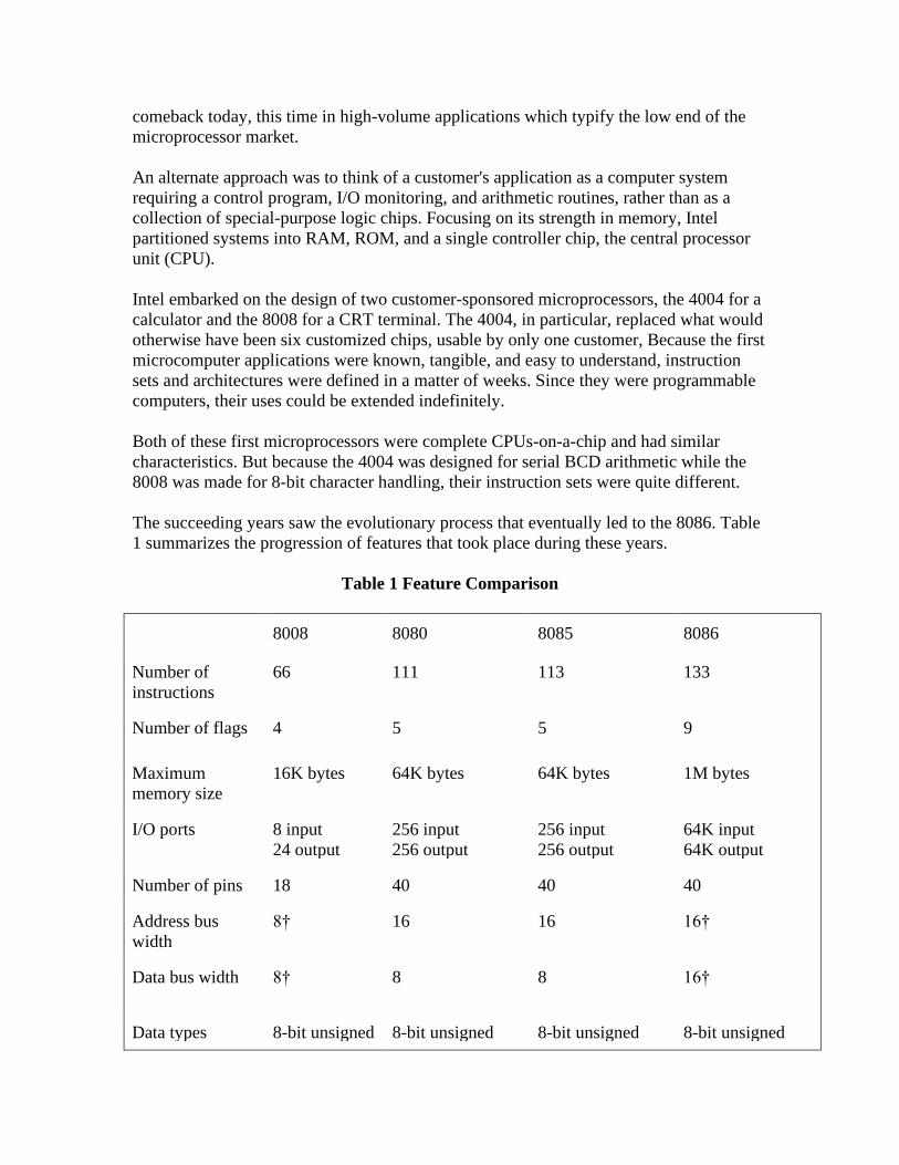
The succeeding years saw the evolutionary process that eventually led to the 8086. Table
1 summarizes the progression of features that took place during these years.
Table 1 Feature Comparison
8008 8080 8085 8086
Number of
instructions
66 111 113 133
Number of flags 4 5 5 9
Maximum
memory size
16K bytes 64K bytes 64K bytes 1M bytes
I/O ports 8 input
24 output
256 input
256 output
256 input
256 output
64K input
64K output
Number of pins 18 40 40 40
Address bus
width
8† 16 16 16†
Data bus width 8† 8 8 16†
Data types 8-bit unsigned 8-bit unsigned 8-bit unsigned 8-bit unsigned
16-bit unsigned
(limited)
Packed BCD
(limited)
16-bit unsigned
(limited)
Packed BCD
(limited)
8-bit signed
16-bit unsigned
16-bit signed
Packed BCD
Unpacked BCD
Addressing
modes
Register ‡
Immediate
Memory direct
(limited)
Memory indirect
(limited)
Register ‡
Immediate
Memory direct
(limited)
Memory indirect
(limited)
Register ‡
Immediate
Memory direct
Memory indirect
Register
Immediate
Indexing
Introduction date 1972 1974 1976 1978
† Address and data bus multiplexed.
‡ Memory can be addressed as a special case by using register M.
II. 8008 Objectives and Constraints
Late in 1969 Intel Corporation was contracted by Computer Terminal Corporation (today
called Datapoint) to do a pushdown stack chip for a processor to be used in a CRT
terminal. Datapoint had intended to build a bit-serial processor in TTL logic using shift-
register memory. Intel counterproposed to implement the entire processor on one chip,
which was to become the 8008. This processor, along with the 4004, was to be fabricated
using the then-current memory fabrication technology, p-MOS. Due to the long lead time
required by Intel, Computer Terminal proceeded to market the serial processor and thus
compatibility constraints were imposed on the 8008.
Most of the instruction-set and register organization was specified by Computer
Terminal. Intel modified the instruction set so the processor would fit on one chip and
added instructions to make it more general-purpose. For although Intel was developing
the 8008 for one particular customer, it wanted to have the option of selling it to others.
Intel was using only 16- and 18-pin packages in those days, and rather than require a new
package for what was believed to be a low-volume chip, they chose to use 18 pins for the
8008.
III. 8008 Instruction-Set Processor
The 8008 processor architecture is quite simple compared to modern-day
microprocessors. The data-handling facilities provide for byte data only. The memory
space is limited to 16K bytes, and the stack is on the chip and limited to a depth of 8. The
instruction set is small but symmetrical, with only a few operand-addressing modes
available. An interrupt mechanism is provided, but there is no way to disable interrupts.
A. Memory and I/O Structure
The 8008 addressable memory space consists of 16K bytes. That seemed like a lot back
in 1970, when memories were expensive and LSI devices were slow. It was
inconceivable in those days that anybody would want to put more than 16K of this
precious resource on anything as slow as a microprocessor.
The memory size limitation was imposed by the lack of available pins. Addresses are sent
out in two consecutive clock cycles over an 8-bit address bus. Two control signals, which
would have been on dedicated pins if these had been available, are sent out together with
every address, thereby limiting addresses to 14 bits.
The 8008 provides eight 8-bit input ports and twenty-four 8-bit output ports. Each of
these ports is directly addressable by the instruction set. It was felt that output ports were
more important than input ports because input ports can always be multiplexed by
external hardware under control of additional output ports.
One of the interesting things about that era was that, for the first time, the users were
given access to the memory bus and could define their own memory structure; they were
not confined to what the vendors offered, as they had been in the minicomputer era. As
an example, the user had the option of putting I/O ports inside the memory address space
instead of in a separate I/O space.
B. Register Structure
The 8008 processor contains two register files and four 1-bit flags. The register flies are
referred to as the scratchpad and the address stack.
1. Scratchpad. The scratchpad file contains an 8-bit accumulator called A and six
additional 8-bit registers called B,C,D,E,H, and L. All arithmetic operations use the
accumulator as one of the operands and store the result back in the accumulator. All
seven registers can be used interchangeably for on-chip temporary storage.
There is one pseudo-register, M, which can be used inter changeably with the scratchpad
registers. M is, in effect, that particular byte in memory whose address is currently
contained in H and L (L contains the eight low-order bits of the address and H contains
the six high-order bits). Thus M is a byte in memory and not a register; although
instructions address M as if it were a register, accesses to M actually involve memory
references. The M register is the only mechanism by which data in memory can be
accessed.
2. Address Stack. The address stack contains a 3-bit stack pointer and eight 14-bit
address registers providing storage for eight addresses. These registers are not directly
accessible by the programmer; rather they are manipulated with control-transfer
instructions.
Any one of the eight address registers in the address stack can serve as the program
counter; the current program counter is specified by the stack pointer. The other seven
address registers permit storage for nesting of subroutines up to seven levels deep. The
execution of a call instruction causes the next address register in turn to become the
current program counter, and the return instruction causes the address register that last
served as the program counter to again become the program counter. The stack will wrap
around if subroutines are nested more than seven levels deep.
3. Flags. The four flags in the 8008 are CARRY, ZERO, SIGN, and PARITY. They are
used to reflect the status of the latest arithmetic or logical operation. Any of the flags can
be used to alter program flow through the use of the conditional jump, call, or return
instructions. There is no direct mechanism for saving or restoring flags, which places a
severe burden on interrupt processing (see Appendix 1 for details).
The CARRY flag indicates if a carry-out or borrow-in was generated, thereby providing
the ability to perform multiple-precision binary arithmetic.
The ZERO flag indicates whether or not the result is zero. This provides the ability to
compare the two values for equality.
The SIGN flag reflects the setting of the leftmost bit of the result. The presence of this
flag creates the illusion that the 8008 is able to handle signed numbers. However, there is
no facility for detecting signed overflow on additions and subtractions. Furthermore,
comparing signed numbers by subtracting them and then testing the SIGN flag will not
give the correct result if the subtraction resulted in signed overflow. This oversight was
not corrected until the 8086.
The PARITY flag indicates if the result is even or odd parity. This permits testing for
transmission errors, an obviously useful function for a CRT terminal.
C. Instruction Set
The 8008 instructions are designed for moving or modifying 8-bit operands. Operands
are either contained in the instruction itself (immediate operand), contained in a
scratchpad register (register operand), or contained in the M register (memory operand).
Since the M register can be used interchangeably with the scratchpad registers, there are
only two distinct operand-addressing modes – immediate and register. Typical instruction
formats for these modes are shown in Figure 1.
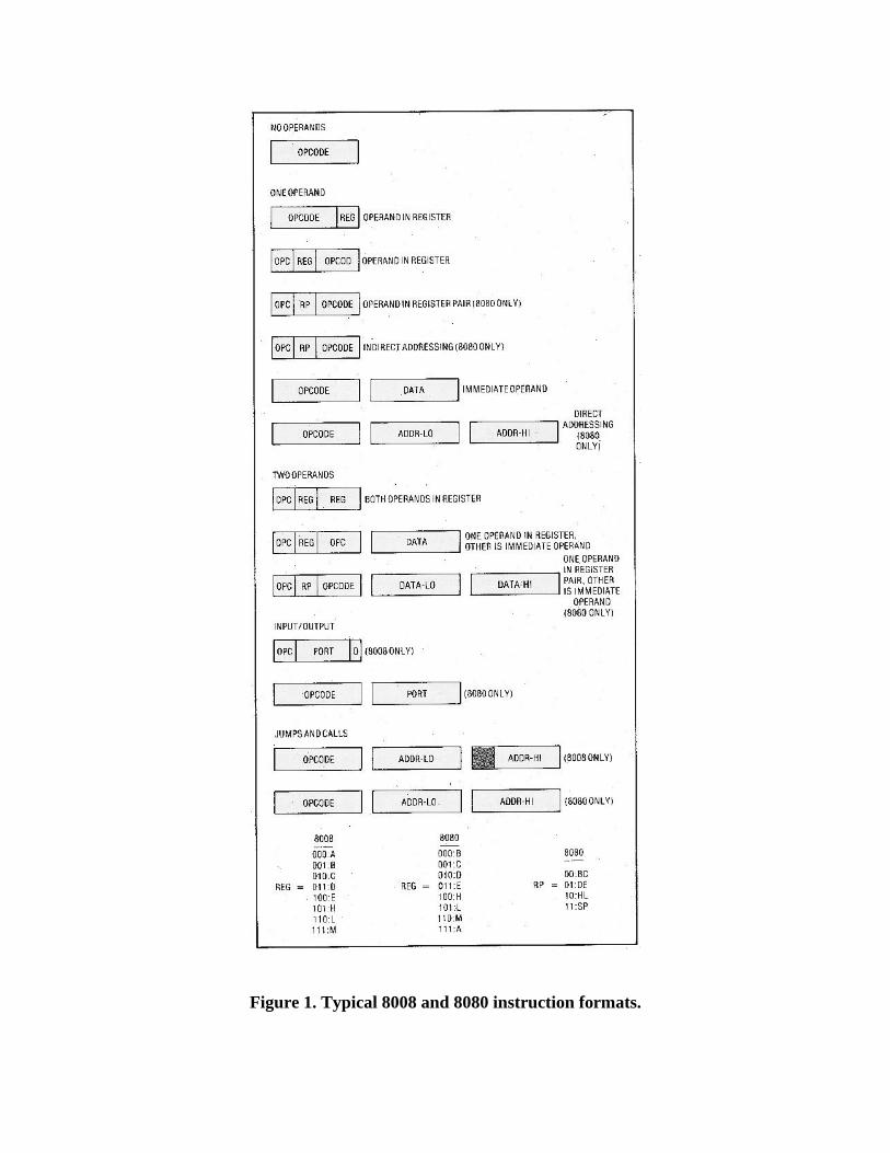
Figure 1. Typical 8008 and 8080 instruction formats.
The instruction set consists of scratchpad-register instructions, accumulator-specific
instructions, transfer-of-control instructions, input/output instructions, and processor-
control instructions.
The scratchpad-register instructions modify the contents of the M register or any
scratchpad register. This can consist of moving data between any two registers, moving
immediate data into a register, or incrementing or decrementing the contents of a register.
The incrementing and decrementing instructions were not in Computer Terminal's
specified instruction set; they were added by Intel to provide for loop control, thereby
making the processor more general-purpose.
Most of the accumulator specific instructions perform operations between the
accumulator and a specified operand. The operand can be any one of the scratchpad
registers, including M, or it can be immediate data. The operations are add, add-with-
carry, subtract, subtract-with-borrow, logical AND, logical OR, logical exclusive-OR,
and compare. Furthermore, there are four unit-rotate instructions that operate on the
accumulator. These instructions perform either an 8- or 9-bit rotate (the CARRY flag acts
as a ninth bit) in either the left or right direction.
Transfer-of-control instructions consist of jumps, calls, and returns. Any of the transfers
can be unconditional, or can be conditional based on the setting of any one of the four
flags. Making calls and returns conditional was done to preserve the symmetry with
jumps and for no other reason. A short one-byte form of call is also provided, which will
be discussed later under interrupts.
Each of the jump and call instructions (with the exception of the one-byte call) specifies
an absolute code address in the second and third byte of the instruction. The second byte
contains the eight low-order bits of the address, and the third byte contains the six high-
order bits. This inverted storage, which was to haunt all processors evolved from the
8008, was a result of compatibility with the Datapoint bit-serial processor, which
processes addresses from low bit to high bit. This inverted storage did have a virtue in
those early days when 256 by 8 memory chips were popular: it allowed all memory chips
to select a byte and latch it for output while waiting for the six high-order bits which
selected the chip. This speeded up memory access.
There are eight input instructions and 24 output instructions, which altogether use up 32
opcodes. Each of these instructions transfers a byte of data between the accumulator and
a designated I/O port.
The processor-control instructions are halt and no-op. Halt puts the processor into a
waiting state. The processor will remain in that state until an interrupt occurs. No-op is
actually one of the move instructions; specifically, it moves the contents of the
accumulator into the accumulator, thereby having no net effect (move instructions do not
alter flag settings).
D. Interrupts
Interrupt processing was not a requirement of the 8008. Hence only the most primitive
mechanism conceivable-not incrementing the program counter-was provided. Such a
mechanism permits an interrupting device to jam an instruction into the processor's
instruction stream. This is accomplished by having the interrupting device, instead of
memory, respond to the instruction fetch; since the program counter isn't incremented,
the instruction in memory that doesn't get fetched won't be skipped. The instruction
typically supplied by the interrupting device is a call, so that an interrupt service routine
can be entered and then the main program can be resumed after interrupt processing is
complete (a jump instruction would result in the loss of the main program return address).
To simplify the interrupting device's task of generating an instruction, the 8008
instruction set provides eight one-byte subroutine calls, each to a fixed location in
memory.
There are no instructions provided for disabling the interrupt mechanism, and so this
function must be realized with external hardware. More important, there are no
instructions for conveniently saving the registers and flags when an interrupt occurs.
IV. Objectives and Constraints of the 8080
By 1973 the technology had advanced from p-MOS to n-MOS for memory fabrication.
As an engineering exercise it was decided to use the 8008 layout masks with the n-MOS
process to obtain a faster 8008. After a short study, it was determined that a new layout
was required, so it was decided to enhance the processor at the same time, and to utilize
the new 40-pin package made practical by high-volume calculator chips. The result was
the 8080 processor.
The 8080 was the first processor designed specifically for the microprocessor market. It
was constrained to include all the 8008 instructions but not necessarily with the same
encodings. This meant that user's software would be portable but the actual ROM chips
containing the programs would have to be replaced. The main objective of the 8080 was
to obtain a 10:1 improvement in throughput, eliminate many of the 8008 shortcomings
that had by then become apparent, and provide new processing capabilities not found in
the 8008. These included a commitment to 16-bit data types mainly for address
computations, BCD arithmetic, enhanced operand-addressing modes, and improved
interrupt capabilities. Now that memory costs had come down and processing speed was
approaching TTL, larger memory spaces were appearing more practical. Hence another
goal was to be able to address directly more than 16K bytes. Symmetry was not a goal,
because the benefits to be gained from making the extensions symmetric would not
justify the resulting increase in chip size and opcode space.
V. The 8080 Instruction-Set Processor
The 8080 architecture is an unsymmetrical extension of the 8008. The byte-handling
facilities have been augmented with a limited number of 16-bit facilities. The memory
space grew to 64K bytes and the stack was made virtually unlimited.
Various alternatives for the 8080 were considered. The simplest involved merely adding
a memory stack and stack instructions to the 8008. An intermediate position was to
augment the above with 16-bit arithmetic facilities that can be used for explicit address
manipulations as well as 16-bit data manipulations. The most difficult alternative was a
symmetric extension which replaced the one-byte M-register instructions with three-byte
generalized memory-access instructions. The last two bytes of these instructions
contained two address-mode bits specifying indirect addressing and indexing (using HL
as an index register) and a 14-bit displacement. Although this would have been a more
versatile addressing mechanism, it would have resulted in significant code expansion on
existing 8008 programs. Furthermore, the logic necessary to implement this solution
would have precluded the ability to implement 16-bit arithmetic; such arithmetic would
not be needed for address manipulations under this enhanced addressing facility but
would still be desirable for data manipulations. For these reasons, the intermediate
position was finally taken.
A. Memory and I/O Structure
The 8080 can address up to 64K bytes of memory, a fourfold increase over the 8008 (the
14-bit address stack of the 8008 was eliminated). The address bus of the 8080 is 16 bits
wide, in contrast to eight bits for the 8008, so an entire address can be sent down the bus
in one memory cycle. Although the data handling facilities of the 8080 are primarily
byte-oriented (the 8008 was exclusively byte-oriented), certain operations permit two
consecutive bytes of memory to be treated as a single data item. The two bytes are called
a word. The data bus of the 8080 is only eight bits wide, and hence word accesses require
an extra memory cycle.
The most significant eight bits of a word are located at the higher memory address. This
results in the same kind of inverted storage already noted in transfer instructions of the
8008.
The 8080 extends the 32-port capacity of the 8008 to 256 input ports and 256 output
ports. In this instance, the 8080 is actually more symmetrical than the 8008. Like the
8008, all of the ports are directly addressable by the instruction set.
B. Register Structure
The 8080 processor contains a file of seven 8-bit general registers, a 16-bit program
counter (PC) and stack pointer (SP), and five 1-bit flags. A comparison between the 8008
and 8080 register sets is shown in Figure 2.
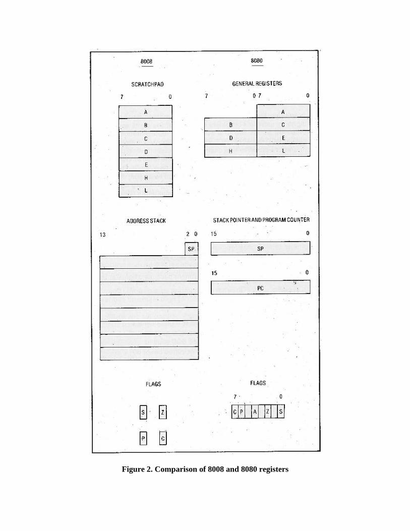
Figure 2. Comparison of 8008 and 8080 registers
1. General Registers. The 8080 registers are the same seven 8-bit registers that were in
the 8008 scratchpad-namely A,B,C, D,E,H, and L. In order to incorporate 16-bit data
facilities in the 8080, certain instructions operate on the register pairs BC, DE, and HL.
The seven registers can be used interchangeably for on-chip temporary storage. The three
register pairs are used for address manipulations, but their roles are not interchangeable;
there is an 8080 instruction that allows operations on DE and not BC, and there are
address modes that access memory indirectly through BC or. DE but not HL.
As in the 8008, the A register has a unique role in arithmetic and logical operations: it
serves as one of the operands and is the receptacle for the result. The HL register again
has its special role of pointing to the pseudo-register M.
2. Stack Pointer and Program Counter. The 8080 has a single program counter instead
of the floating program counter of the 8008. The program counter is 16 bits (two bits
more than the 8008's program counter), thereby permitting an address space of 64K.
The stack is contained in memory instead of on the chip, which removes the restriction of
only seven levels of nested subroutines. The entries on the stack are 16 bits wide. The 16-
bit stack pointer is used to locate the stack in memory. The execution of a call instruction
causes the contents of the program counter to be pushed onto the stack, and the return
instruction causes the last stack entry to be popped into the program counter. The stack
pointer was chosen to run "downhill" (with the stack advancing toward lower memory) to
simplify indexing into the stack from the user's program (positive indexing) and to
simplify displaying the contents of the stack from a front panel.
Unlike the 8008, the stack pointer is directly accessible to the programmer. Furthermore,
the stack itself is directly accessible, and instructions are provided that permit the
programmer to push and pop his own 16-bit items onto the stack.
3. Flags. A fifth flag, AUXILIARY CARRY, augments the 8008 flag set to form the flag
set of the 8080. The AUXILIARY CARRY flag indicates if a carry was generated out of
the four low-order bits. This flag, in conjunction with a decimal-adjust instruction,
provides the ability to perform packed BCD addition (see Appendix 2 for details). This
facility can be traced back to the 4004 processor. The AUXILIARY CARRY flag has no
purpose other than for BCD arithmetic, and hence the conditional transfer instructions
were not expanded to include tests on the AUXILIARY CARRY flag.
It was proposed too late in the design that the PARITY flag should double as an
OVERFLOW flag. Although this feature didn't make it into the 8080, it did show up two
years later in Zilog's Z-80.
C. Instruction Set
The 8080 includes the entire 8008 instruction set as a subset, The added instructions
provide some new operand-addressing modes and some facilities for manipulating 16-bit
data. These extensions have introduced a good deal of asymmetry. Typical instruction
formats are shown in Figure 1
The only means that the 8008 had for accessing operands in memory was via the M
register. The 8080 has certain instructions that access memory by specifying the memory
address (direct addressing) and also certain instructions that access memory by specifying
a pair of general registers in which the memory address is contained (indirect addressing).
In addition, the 8080 includes the register and immediate operand-addressing modes of
the 8008. A 16-bit immediate mode is also included.
The added instructions can be classified as load/store instructions, register-pair
instructions, HL-specific instructions, accumulator-adjust instructions, carry instructions,
expanded I/O instructions, and interrupt instructions.
The load/store instructions load and store the accumulator register and the HL register
pair using the direct and indirect addressing mode. Both modes can be used for the
accumulator, but due to chip size constraints, only the direct mode was implemented for
HL.
The register-pair instructions provide for the manipulation of 16-bit data items.
Specifically, register pairs can be loaded with 16-bit immediate data, incremented,
decremented, added to HL, pushed on the stack, or popped off the stack. Furthermore, the
flag settings themselves can be pushed and popped, thereby simplifying saving the
environment when interrupts occur (this was not possible in the 8008).
The HL-specific instructions include facilities for transferring HL to the program counter
or to the stack pointer, and exchanging HL with DE or with the top entry on the stack.
The last of these instructions was included to provide a mechanism for (1) removing a
subroutine return address from the stack so that passed parameters can be discarded or (2)
burying a result-to-be-returned under the return address, This became the longest
instruction in the 8080 (5 memory cycles); its implementation precluded the inclusion of
several other instructions that were already proposed for the processor.
Two accumulator-adjust instructions are provided. One complements each bit in the
accumulator and the other modifies the accumulator so that it contains the correct
decimal result after a packed BCD addition is performed.
The carry instructions provide for setting or complementing the CARRY flag. No
instruction is provided for clearing the CARRY flag. Because of the way the CARRY
flag semantics are defined, the CARRY flag can be cleared simply by ORing or ANDing
the accumulator with itself.
The expanded I/O instructions permit transferring the contents of any one of 256 8-bit
ports either to or from the accumulator. The port number is explicitly contained in the
instruction; hence, the instruction is two bytes long. The equivalent 8008 instruction is
only one byte long. This is the only instance in which an 8080 instruction requires a
different number of bytes than its 8008 counterpart. The motivation for doing this was
more to free up 32 opcodes than to increase the number of I/O ports.
The 8080 has the identical interrupt mechanism the 8008 has, but in addition, it has
instructions for enabling or disabling the interrupt mechanism. This feature, along with
the ability to push and pop the processor flags, made the interrupt mechanism practical.
VI. 8085 Objectives and Constraints
In 1976, technology advances allowed Intel to consider enhancing its 8080. The objective
was to come out with a processor set utilizing a single power supply and requiring fewer
chips (the 8080 required a separate oscillator chip and system controller chip to make it
usable). The new processor, called the 8085, was constrained to be compatible with the
8080 at the machine-code level. This meant that the only extension to the instruction set
could be in the twelve unused opcodes of the 8080.
The 8085 turned out to be architecturally not much more than a repackaging of the 8080.
The major differences were in such areas as an on-chip oscillator, power-on reset,
vectored interrupts, decoded control lines, a serial I/O port, and a single power supply.
Two new instructions, RIM and SIM, were added to handle the serial port and interrupt
mask. Several other instructions that had been contemplated were not made available
because of the software ramifications and the compatibility constraints they would place
on the forthcoming 8086.
VII. Objectives and Constraints of 8086
The new Intel 8086 microprocessor was designed to provide an order of magnitude
increase in processing throughput over the older 8080. The processor was to be assembly-
language-level-compatible with the 8080 so that existing 8080 software could be
reassembled and correctly executed on the 8086. To allow for this, the 8080 register set
and instruction set appear as logical subsets of the 8086 registers and instructions. By
utilizing a general-register structure architecture, Intel could capitalize on its experience
with the 8080 to obtain a processor with a higher degree of sophistication. Strict 8080
compatibility, however, was not attempted, especially in areas where it would
compromise the final design.
The goals of the 8086 architectural design were to provide symmetric extensions of
existing 8080 features, and to add processing capabilities not found in the 8080. These
features included 16-bit arithmetic, signed 8- and 16-bit arithmetic (including multiply
and divide), efficient interruptible byte-string operations, improved bit-manipulation
facilities, and mechanisms to provide for re-entrant code, position-independent code, and
dynamically relocatable programs.
By now memory had become very inexpensive and microprocessors were being used in
applications that required large amounts of code and/or data. Thus another design goal
was to be able to address directly more than 64k bytes and support multiprocessor
configurations.
VIII. The 8086 Instruction-Set Processor
The 8086 processor architecture is described in terms of its memory structure, register
structure, instruction set, and external interface. The 8086 memory structure includes up
to one megabyte of memory space and up to 64K input/output ports. The register
structure includes three files of registers. Four 16-bit general registers can participate
interchangeably in arithmetic and logic operations, two 16-bit pointer and two 16-bit
index registers are used for address calculations, and four 16-bit segment registers allow
extended addressing capabilities. Nine flags record the processor state and control its
operation.
The instruction set supports a wide range of addressing modes and provides operations
for data transfer, signed and unsigned 8- and 16-bit arithmetic, logicals, string
manipulations, control transfer, and processor control. The external interface includes a
reset sequence, interrupts, and a multiprocessor-synchronization and resource-sharing
facility.
A. Memory Structure
The 8086 memory structure consists of two components-the memory space and the
input/output space. All instruction code and operands reside in the memory space.
Peripheral and I/O devices ordinarily reside in the I/O space, except in the case of
memory-mapped devices.
1. Memory Space. The 8086 memory is a sequence of up to 1 million 8-bit bytes, a
considerable increase over the 64K bytes in the 8080. Any two consecutive bytes may be
paired together to form a 16-bit word. Such words may be located at odd or even byte
addresses. The data bus of the 8086 is 16 bits wide, so, unlike the 8080, a word can be
accessed in one memory cycle (however, words located at odd byte addresses still require
two memory cycles). As in the 8080, the most significant 8 bits of a word are located in
the byte with the higher memory address.
Since the 8086 processor performs 16-bit arithmetic, the address objects it manipulates
are 16 bits in length. Since a 16-bit quantity can address only 64K bytes, additional
mechanisms are required to build addresses in a megabyte memory space. The 8086
memory may be conceived of as an arbitrary number of segments, each at most 64K
bytes in size. Each segment begins at an address which is evenly divisible by 16 (i.e., the
low-order 4 bits of a segment's address are zero). At any given moment the contents of
four of these segments are immediately addressable. These four segments, called the
current code segment, the current data segment, the current stack segment, and the
current extra segment, need not be unique and may overlap. The high-order 16 bits of the
address of each current segment are held in a dedicated 16-bit segment register. In the
degenerate case where all four segments start at the same address, namely address 0, we
have an 8080 memory structure.
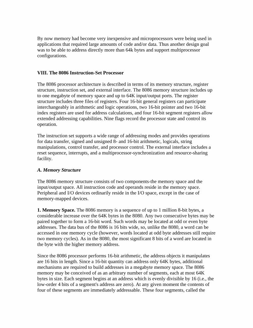
Bytes or words within a segment are addressed by using 16-bit offset addresses within the
64K byte segment. A 20-bit physical address is constructed by adding the 16-bit offset
address to the contents of a 16-bit segment register with 4 low-order zero bits appended,
as illustrated in Figure 3.
Figure 3. Addressing one million bytes requires a 20-bit memory address. This 20-
bit address is constructed by offsetting the effective address four bits to the right of
the segment address, filling in the four low-order bits of the segment address wit
zeroes, and then adding the two.
Various alternatives for extending the 8080 address space were considered. One such
alternative consisted of appending 8 rather than 4 low-order zero bits to the contents of a
segment register, thereby providing a 24-bit physical address capable of addressing up to
16 megabytes of memory. This was rejected for the following reasons:
Segments would be forced to start on 256-byte boundaries, resulting in excessive
memory fragmentation.
The 4 additional pins that would he required on the chip were not available.
It was felt that a 1-megabyte address space was sufficient.
2. Input/Output Space. In contrast to the 256 I/O ports in the 8080, the 8086 provides
64K addressable input or output ports. Unlike the memory, the I/O space is addressed as
if it were a single segment, without the use of segment registers. Input/output physical
addresses are in fact 20 bits in length, but the high-order 4 bits are always zero. The first
256 ports are directly addressable (address in the instruction), whereas all 64K ports are
indirectly addressable (address in register). Such indirect addressing was provided to
permit consecutive ports to he accessed in a program loop. Ports may be 8 or 16 bits in
size, and 16-bit ports may he located at odd or even addresses.
B. Register Structure
The 8086 processor contains three files of four 16-bit registers and a file of nine 1-bit
flags. The three files of registers are the general-register file, the pointer- and index-
register file, and the segment-register file. There is a 16-bit instruction pointer (called the
program counter in the earlier processors) which is not directly accessible to the
programmer; rather, it is manipulated with control transfer instructions. The 8086 register
set is a superset of the 8080 registers, as shown in Figures 4 and 5. Corresponding
registers in the 8080 and 8086 do not necessarily have the same names, thereby
permitting the 8086 to use a more meaningful set of names.
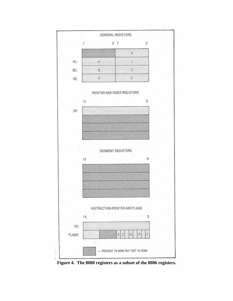
Figure 4. The 8080 registers as a subset of the 8086 registers.
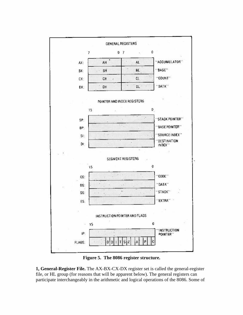
Figure 5. The 8086 register structure.
1, General-Register File. The AX-BX-CX-DX register set is called the general-register
file, or HL group (for reasons that will be apparent below). The general registers can
participate interchangeably in the arithmetic and logical operations of the 8086. Some of
the other 8086 operations (such as the string operations) dedicate certain of the general
registers to specific uses. These uses are indicated by the mnemonic phrases
"accumulator," "base," "count," and "data" in Figure 5. The general registers have a
property that distinguishes them from the other registers-their upper and lower halves are
separately addressable. Thus, the general registers can be thought of as two files of four
8-bit registers-the H (high-order) file and the L (low-order) file.
2. Pointer- and Index-Register File. The SP-BP-SI-DI register set is called the pointer-
and index-register file, or the P and I groups. The registers in this file generally contain
offset addresses used for addressing within a segment. Like the general registers, the
pointer and index registers can participate interchangeably in the 16-bit arithmetic and
logical operations of the 8086, thereby providing a means to perform address
computations. These registers play a major role in effective address computations, as
described in the section on Operand Addressing below (Sec. VIII. C. 1.).
There is one main difference between the registers in this file, which results in dividing
the file into two subfiles, the P or pointer group (SP,BP) and the I or index group (SI,DI).
The difference is that the pointers are by default assumed to contain offset addresses
within the current stack segment, and the indexes are by default generally assumed to
contain offset addresses within the current data segment. The mnemonic phrases "stack
pointer," "base pointer," "source index," and "destination index" are mnemonics
associated with these registers' names, as shown in Figure 5.
3. Segment-Register File. The CS-DS-SS-ES register set is called the segment-register
file, or S group. The segment registers play an important role in the memory addressing
mechanism of the processor. These registers are similar in that they are used in all
memory address computations (see Sec. VIII. A. of this chapter). The segment registers
names have the associated mnemonic phrases "code," "data," "stack," and "extra as
shown in Figure 5.
The contents of the CS register define the current code segment. All instruction fetches
are taken to be relative to CS, using the instruction pointer (IP) as an offset. The contents
of the DS register define the current data segment. Generally, all data references except
those involving BP or SP are taken by default to be relative to DS. The contents of the SS
register define the current stack segment. All data references which explicitly or
implicitly involve SP or BP are taken by default to be relative to SS. This includes all
push and pop operations, interrupts, and return operations. The contents of the ES register
define the current extra segment. The extra segment has no specific use, although it is
usually treated as an additional data segment which can be specified in an instruction by
using a special default-segment-override prefix.
In general, the default segment register for the two types of data references (DS and SS)
can be overriden. By preceding the instruction with a special one-byte prefix, the
reference can be forced to be relative to one of the other three segment registers. This
prefix, as well as other prefixes described later, has a unique encoding that permits it to
be distinguished from the opcodes.
Programs which do not load or manipulate the segment registers are said to be
dynamically relocatable. Such a program may be interrupted, moved in memory to a new
location, and restarted with new segment-register values.
At first a set of eight segment registers was proposed along with a field in a program-
status word specifying which segment register was currently CS, which was currently
DS, and which was currently SS. The other five all served as extra segment registers.
Such a scheme would have resulted in virtually no thrashing of segment register contents;
start addresses of all needed segments would be loaded initially into one of the eight
segment registers, and the roles of the various segment registers would vary dynamically
during program execution. Concern over the size of the resulting processor chip forced
the number of segment registers to be reduced to the minimum number necessary, namely
four. With this minimum number, each segment register could be dedicated to a
particular type of segment (code, data, stack, extra), and the specifying field- in the
program status word was no longer needed.
4. Flag-Register File. The AF-CF-DF-IF-OF-PF-SF-TF-ZF register set is called the flag-
register file or F group. The flags in this group are all one bit in size and are used to
record processor status information and to control processor operation. The flag registers'
names have the following associated mnemonic phrases:
AF
CF
DF
IF
OF
PF
SF
TF
ZF
Auxiliary carry
Carry
Direction
Interrupt enable
Overflow
Parity
Sign
Trap
Zero
The AF, CF, PE, SF, and ZF flags retain their familiar 8080 semantics, generally
reflecting the status of the latest arithmetic or logical operation. The OF flag joins this
group, reflecting the signed arithmetic overflow condition. The DF, IF, and TF flags are
used to control certain aspects of the processor. The DF flag controls the direction of the
string manipulations (auto-incrementing or auto-decrementing). The IF flag enables or
disables external interrupts. The TF flag puts the processor into a single-step mode for
program debugging. More detail is given on each of these three flags later in the chapter.
C. Instruction Set
The 8086 instruction set-while including most of the 8080 set as a subset-has more ways
to address operands and more power in every area. It is designed to implement block-
structured languages efficiently. Nearly all instructions operate on either 8- or 16-bit
operands. There are four classes of data transfer. All four arithmetic operations are
available. An additional logic instruction, test, is included. Also new are byte- and word-
string manipulations and intersegment transfers.
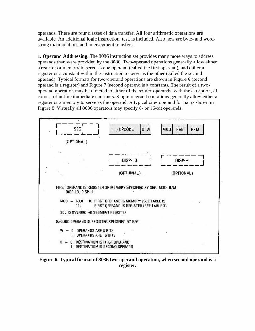
1. Operand Addressing. The 8086 instruction set provides many more ways to address
operands than were provided by the 8080. Two-operand operations generally allow either
a register or memory to serve as one operand (called the first operand), and either a
register or a constant within the instruction to serve as the other (called the second
operand). Typical formats for two-operand operations are shown in Figure 6 (second
operand is a register) and Figure 7 (second operand is a constant). The result of a two-
operand operation may be directed to either of the source operands, with the exception, of
course, of in-line immediate constants. Single-operand operations generally allow either a
register or a memory to serve as the operand. A typical one- operand format is shown in
Figure 8. Virtually all 8086 operators may specify 8- or 16-bit operands.
Figure 6. Typical format of 8086 two-operand operation, when second operand is a
register.
Figure 7. Typical format of 8086 two-operand operation, when second operand is a
constant (immediate data).
Figure 8. Typical format of 8086 one-operand operation.
Memory operands. An instruction may address an operand residing in memory in one of
four ways as determined by the mod and rim fields in the instruction (see Table 2).
Direct 16-bit offset address
Indirect through a base register (BP or BX), optionally with an 8- or 16-bit
displacement
Indirect through an index register (SI or DI), optionally with an 8- or 16-bit
displacement
Indirect through the sum of a base register and an index register, optionally with
an 8- or 16-bit displacement
The general register, BX, and the pointer register, BP, may serve as base registers. When
the base register EX is used without an index register, the operand by default resides in
the current data segment. When the base register BP is used without an index register, the
operand by default resides in the current stack segment. When both base and index
registers are used, the operand by default resides in the segment determined by the base
register. When an index register alone is used, the operand by default resides in the
current data segment.
Auto-incrementing and auto-decrementing address modes were not included in general,
since it was felt that their use is mainly oriented towards string processing. These modes
were included on the string primitive instructions.
Register operands. The four 16-bit general registers and the four 16-bit pointer and index
registers may serve interchangeably as operands in 16-bit operations. Three exceptions to
note are multiply, divide, and the string operations, all of which use the AX register
implicitly. The eight 8-bit registers of the HL group may serve interchangeably in 8-bit
operations. Again, multiply, divide, and the string operations use AL implicitly. Table 3
shows the register selection as determined by the r/m field (first operand) or reg field
(second operand) in the instruction.
Immediate operands. All two-operand operations except multiply, divide, and the string
operations allow one source operand to appear within the instruction as immediate data
represented in 2's complement form. Sixteen-bit immediate operands having a high-order
byte which is the sign extension of the low-order byte may be abbreviated to 8 bits.
Addressing mode usage. The addressing modes permit registers BX and BP to serve as
base registers and registers SI and DI as index registers. Possible use of this for language
implementation is discussed below.
Simple variables and arrays: A simple variable is accessed with the direct address
mode. An array element is accessed with the indirect address mode utilizing the
sum of the register SI (where SI contains the index into the array) and
displacement (where displacement is the offset of the array in its segment).
Based variables: A based variable is located at a memory address pointed at by
some other variable. If the contents of the pointer variable were placed in BX, the
indirect addressing mode utilizing BX would access the based variable. If the
based variable were an array and the index into the array were placed in SI, the
indirect addressing mode utilizing the sum of the register BX and register SI
would access elements of the array.
Stack marker: Marking a stack permits efficient implementation of block-
structured languages and provides an efficient address mechanism for reentrant
procedures. Register BP can be used as a stack marker pointer to the beginning of
an activation record in the stack. The indirect address mode utilizing the sums of
the base register BP and a displacement (where displacement is the offset of a
local variable in the activation record) will access the variable declared in the
currently active block. The indirect address mode utilizing the sum of the base
register BP, index register SI (where SI contains the index in an array), and
displacement (where displacement is the offset of the array in the activation
record) will access an element of the array. Register DI can be used in the same
manner as SI so that two array elements can be accessed concurrently.
Example: An example of a procedure-calling sequence on the 8086 illustrates the
interaction of the addressing modes and activation records.
;CALL MYPROC (ALPHA, BETA) PUSH ALPHA ;pass parameters by pushing them on the stack PUSH BETA CALL MYPROC ;call the procedure ;PROCEDURE MYPROC (A, B) MYPROC: ;entry point PUSH BP ;save previous BP value MOV BP,SP ;make BP point at new record SUB SP,LOCALS ;allocate local storage on stack ;... for reentrant procedures (stack advances towards lower memory) ;body of procedure MOV SP,BP ;deallocate local storage POP BP ;restore previous BP RET 4 ;return and discard 4 bytes of parameters
Upon entry to the procedure MYPROC its parameters are addressable with
positive offsets from BP (the stack grows towards lower memory addresses).
Since usually less than 128 bytes of parameters are passed, only an 8-bit signed
displacement from BP is needed. Similarly, local variables to MYPROC are
addressable with negative offsets from BP. Again, economy of instruction size is
realized by using 8-bit signed displacements. A special return instruction discards
the parameters pushed on the stack.
Table 2 Determining 8086 Offset Address of a Memory Operand
(Use This Table When mod ≠ 11; Otherwise Use Table 3.)
This table applies to the first operand only; the second operand can never be a
memory operand.
mod specifies how disp-lo and disp-hi are used to define a displacement as
follows:
mod = 00: DISP=0 (disp-lo and disp-hi are absent)
mod = 01: DISP=disp-lo sign extended (disp-hi is absent)
mod = 10: DISP = disp-hi,disp-lo
r/m specifies which base and index register contents are to be added to the
displacement to form the operand offset address as follows:
r/m = 000: OFFSET = (BX) + (SI) + DISP (indirect address mode)
r/m = 001: OFFSET = (BX) + (DI) + DISP (indirect address mode)
r/m = 010: OFFSET = (BP) + (SI) + DISP (indirect address mode)
r/m = 011: OFFSET = (BP) + (DI) + DISP (indirect address mode)
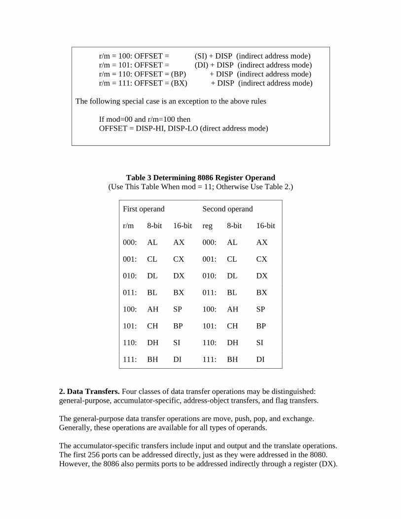
r/m = 100: OFFSET = (SI) + DISP (indirect address mode)
r/m = 101: OFFSET = (DI) + DISP (indirect address mode)
r/m = 110: OFFSET = (BP) + DISP (indirect address mode)
r/m = 111: OFFSET = (BX) + DISP (indirect address mode)
The following special case is an exception to the above rules
If mod=00 and r/m=100 then
OFFSET = DISP-HI, DISP-LO (direct address mode)
Table 3 Determining 8086 Register Operand
(Use This Table When mod = 11; Otherwise Use Table 2.)
First operand Second operand
r/m 8-bit 16-bit reg 8-bit 16-bit
000: AL AX 000: AL AX
001: CL CX 001: CL CX
010: DL DX 010: DL DX
011: BL BX 011: BL BX
100: AH SP 100: AH SP
101: CH BP 101: CH BP
110: DH SI 110: DH SI
111: BH DI 111: BH DI
2. Data Transfers. Four classes of data transfer operations may be distinguished:
general-purpose, accumulator-specific, address-object transfers, and flag transfers.
The general-purpose data transfer operations are move, push, pop, and exchange.
Generally, these operations are available for all types of operands.
The accumulator-specific transfers include input and output and the translate operations.
The first 256 ports can be addressed directly, just as they were addressed in the 8080.
However, the 8086 also permits ports to be addressed indirectly through a register (DX).
This latter facility allows 64K ports to be addressed. Furthermore, the 8086 ports may be
8 or 16 bits wide, whereas the 8080 only permitted 8-bit-wide ports. The translate
operation performs a table-lookup byte translation. We will see the useful ness of this
operation below, when it is combined with string operations.
The address-object transfers – load effective address and load pointer – are an 8086
facility not present in the 8080. A pointer is a pair of 16-bit values specifying a segment
start address and an offset address; it is used to gain access to the full megabyte of
memory. The load pointer operations provide a means of loading a segment start address
into a segment register and an offset address into a general or pointer register in a single
operation. The load effective address operation provides access to the offset address of an
operand, as opposed to the value of the operand itself.
The flag transfers provide access to the collection of flags for such operations as push,
pop, load, and store. A similar facility for pushing and popping flags was provided in the
8080; the load and store flags facility is new in the 8086.
It should he noted that the load and store operations involve only those flags that existed
in the 8080. This is part of the concessions made for 8080 compatibility (without these
operations it would take nine 8086 bytes to perform exactly an 8080 PUSH PSW or POP
PSW).
3. Arithmetics. Whereas the 8080 provided for only 8-bit addition and subtraction of
unsigned numbers, the 8086 provides all four basic mathematical functions on 8- and 16-
bit signed and unsigned numbers. Standard 2's complement representation of signed
values is used. Sufficient conditional transfers are provided to allow both signed and
unsigned comparisons. The OF flag allows detection of the signed overflow condition.
Consideration was given to providing separate operations for signed addition and
subtraction which would automatically trap on signed overflow (signed overflow is an
exception condition, whereas unsigned overflow is not). However, lack of room in the
opcode space prohibited this. As a compromise, a one-byte trap-on-overflow instruction
was included to make testing for signed overflow less painful.
The 8080 provided a correction operation to allow addition to be performed directly on
packed binary-coded representations of decimal digits. In the 8086, correction operations
are provided to allow arithmetic to be performed directly on unpacked representations of
decimal digits (e.g., ASCII) or on packed decimal representations.
Multiply and divide. Both signed and unsigned multiply and divide operations are
provided. Multiply produces a double-length product (16 bits for 8-bit multiply, 32 bits
for 16-bit multiply), while divide returns a single-length quotient and a single-length
remainder from a double-length dividend and single-length divisor. Sign extension
operations allow one to construct the double-length dividend needed for signed division.
A quotient overflow (e.g., that caused by dividing by zero) will automatically interrupt
the processor.
Decimal instructions. Packed BCD operations are provided in the form of accumulator-
adjustment instructions. Two such instructions are provided-one for an adjustment
following an addition and one following a subtraction. The addition adjustment is
identical to the 8080 DAA instruction; the subtraction adjustment is defined similarly.
Packed multiply and divide adjustments are not provided, because the cross terms
generated make it impossible to recover the decimal result without additional processor
facilities (see Appendix 2 for details).
Unpacked BCD operations are also provided in the form of accumulator adjust
instructions (ASCII is a special case of unpacked BCD). Four such instructions are
provided, one each for adjustments involving addition, subtraction, multiplication, and
division. The addition and subtraction adjustments are similar to the corresponding
packed BCD adjustments except that the AH register is updated if an adjustment on AL is
required. Unlike packed BCD, unpacked BCD byte multiplication does not generate cross
terms, so multiplication adjustment consists of converting the binary value in the AL
register into BCD digits in AH and AL; the divide adjustment does the reverse. Note that
adjustments for addition, subtraction, and multiplication are performed following the
arithmetic operation; division adjustment is performed prior to a division operation. See
Appendix 2 for more details on unpacked BCD adjustments.
4. Logicals. The standard logical operations AND, OR, XOR, and NOT are carry-overs
from the 8080. Additionally, the 8086 provides a logical TEST for specific bits. This
consists of a logical AND instruction which sets the flags but does not store the result,
thereby not destroying either operand.
The four unit-rotate instructions in the 8080 are augmented with four unit-shift
instructions in the 8086. Furthermore, the 8086 provides multi-bit shifts and rotates
including an arithmetic right shift.
5. String Manipulation. The 8086 provides a group of 1-byte instructions which perform
various primitive operations for the manipulation of byte or word strings (sequences of
bytes or words). These primitive operations can be performed repeatedly in hardware by
preceding the instruction with a special prefix. The single-operation forms may be
combined to form complex string operations in tight software loops with repetition
provided by special iteration operations. The 8080 did not provide any string-
manipulation facilities.
Hardware operation control. All primitive string operations use the SI register to address
the source operands, which are assumed to be in the current data segment. The DI register
is used to address the destination operands, which reside in the current extra segment.
The operand pointers are incremented or decremented (depending on the setting of the
DF flag) after each operation, once for byte operations and twice for word operations.
Any of the primitive string operation instructions may be preceded with a 1-byte prefix
indicating that the operation is to be repeated until the operation count in CX is satisfied,
The test for completion is made prior to each repetition of the operation. Thus, an initial
operation count of zero will cause zero executions of the primitive operation.
The repeat prefix byte also designates a value to compare with the ZF flag. If the
primitive operation is one which affects the ZF flag and the ZF flag is unequal to the
designated value after any execution of the primitive operation, the repetition is
terminated. This permits the scan operation to serve as a scan-while or a scan-until.
During the execution of a repeated primitive operation the operand pointer registers (SI
and DI) and the operation count register (CX) are updated after each repetition, whereas
the instruction pointer will retain the offset address of the repeat prefix byte (assuming it
immediately precedes the string operation instruction). Thus, an interrupted repeated
operation will be correctly resumed when control returns from the interrupting task.
Primitive string operations. Five primitive string operations are provided:
MOVS moves a string element (byte or word) from the source operand to the
destination operand. As a repeated operation, this provides for moving a string
from one location in memory to another.
CMPS subtracts the string element at the destination operand from the string
element at the source operand and affects the flags but does not return the result.
As a repeated operation this provides for comparing two strings. With the
appropriate repeat prefix it is possible to compare two strings and determine after
which string element the two strings become unequal, thereby establishing an
ordering between the strings.
SCAS subtracts the string element at the destination operand from AL (or AX for
word strings) and affects the flags but does not return the result. As a repeated
operation this provides for scanning for the occurrence of, or departure from, a
given value in the string.
LODS loads a string element from the source operand into AL (or AX for word
strings). This operation ordinarily would not be repeated.
STOS stores a string element from AL (or AX for word strings) into the
destination operand. As a repeated operation this provides for filling a string with
a given value.
Software operation control. The repeat prefix provides for rapid iteration in a hardware-
repeated string operation. Iteration-control operations provide this same control for
implementing software loops to perform complex string operations. These iteration
operations provide the same operation count update, operation completion test, and ZF
flag tests that the repeat prefix provides.
The iteration-control transfer operations perform leading- and trailing-decision loop
control. The destinations of iteration-control transfers must be within a 256-byte range
centered about the instruction.
Four iteration-control transfer operations are provided:
LOOP decrements the CX ("count") register by 1 and transfers if CX is not 0.
LOOPE decrements the CX register by 1 and transfers if CX is not 0 and the ZF
flag is set (loop while equal),
LOOPNE decrements the CX register by 1 and transfers if CX is not 0 and the ZF
flag is cleared (loop while not equal).
JCXZ transfers if the CX register is 0. This is used for skipping over a loop when
the initial count is 0.
By combining the primitive string operations and iteration- control operations with other
operations, it is possible to build sophisticated yet efficient string manipulation routines.
One instruction that is particularly useful in this context is the translate operation; it
permits a byte fetched from one string to be translated before being stored in a second
string, or before being operated upon in some other fashion. The translation is performed
by using the value in the AL register to index into a table pointed at by the BX register.
The translated value obtained from the table then replaces the value initially in the AL
register.
As an example of use of the primitive string operations and iteration-control operations to
implement a complex string operation, consider the following application: An input
driver must translate a buffer of EBCDIC characters into ASCII and transfer characters
until one of several different EBCDIC control characters is encountered. The transferred
ASCII string is to be terminated with an EOT character. To accomplish this, SI is
initialized to point to the beginning of the EBCDIC buffer, DI is initialized to point to the
beginning of the buffer to receive the ASCII characters, BX is made to point to an
EBCDIC-to-ASCII translation table, and CX is initialized to contain the length of the
EBCDIC buffer (possibly empty). The translation table contains the ASCII equivalent for
each EBCDIC character, perhaps with ASCII nulls for illegal characters. The EOT code
is placed into those entries in the table corresponding to the desired EBCDIC stop
characters. The 8086 instruction sequence to implement this example is the following:
JCXZ Empty Next: LODS Ebcbuf ;fetch next EBCDIC character XLAT Table ;translate it to ASCII CMP AL, EOT ;test for EOT STOS Ascbuf ;transfer ASCII character
LOOPNE Next ;continue if not EOT Empty:
The body of this loop requires just seven bytes of code.
6. Transfer of Control. Transfer-of-control instructions (jumps, calls, returns) in the
8086 are of two basic varieties: intrasegment transfers, which transfer control within the
current code segment by specifying a new value for IP, and intersegment transfers, which
transfer control to an arbitrary code segment by specifying a new value for both CS and
IP. Furthermore, both direct and indirect transfers are supported. Direct transfers specify
the destination of the transfer (the new value of IP and possibly CS) in the instruction;
indirect transfers make use of the standard addressing modes, as described previously, to
locate an operand which specifies the destination of the transfer. By contrast, the 8080
provides only direct intrasegment transfers.
Facilities for position-independent code and coding efficiency not found in the 8080 have
been introduced in the 8086. Intrasegment direct calls and jumps specify a self-relative
direct displacement, thus allowing position-independent code. A shortened jump
instruction is available for transfers within a 256-byte range centered about the
instruction, thus allowing for code compaction.
Returns may optionally adjust the SP register so as to discard stacked parameters, thereby
making parameter passing more efficient. This is a more complete solution to the
problem than the 8080 instruction which exchanged the contents of the HL with the top
of the stack.
The 8080 provided conditional jumps useful for determining relations between unsigned
numbers. The 8086 augments these with conditional jumps for determining relations
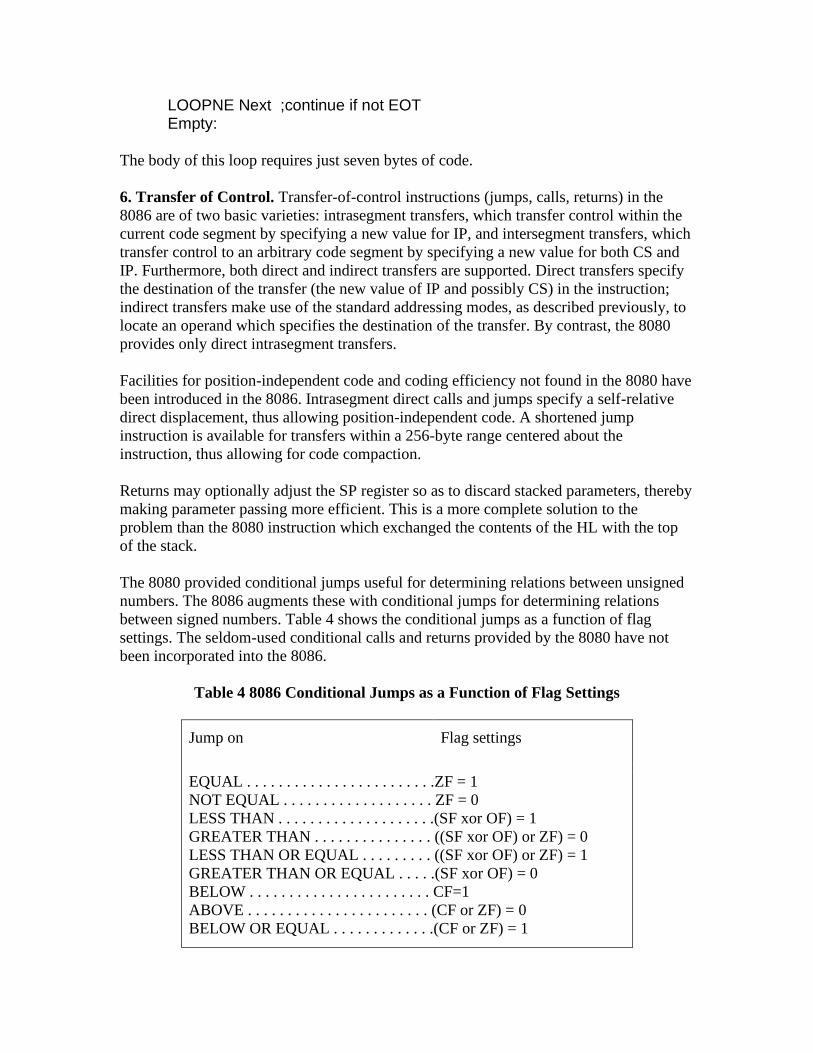
between signed numbers. Table 4 shows the conditional jumps as a function of flag
settings. The seldom-used conditional calls and returns provided by the 8080 have not
been incorporated into the 8086.
Table 4 8086 Conditional Jumps as a Function of Flag Settings
Jump on Flag settings
EQUAL . . . . . . . . . . . . . . . . . . . . . . . .ZF = 1
NOT EQUAL . . . . . . . . . . . . . . . . . . . ZF = 0
LESS THAN . . . . . . . . . . . . . . . . . . . .(SF xor OF) = 1
GREATER THAN . . . . . . . . . . . . . . . ((SF xor OF) or ZF) = 0
LESS THAN OR EQUAL . . . . . . . . . ((SF xor OF) or ZF) = 1
GREATER THAN OR EQUAL . . . . .(SF xor OF) = 0
BELOW . . . . . . . . . . . . . . . . . . . . . . . CF=1
ABOVE . . . . . . . . . . . . . . . . . . . . . . . (CF or ZF) = 0
BELOW OR EQUAL . . . . . . . . . . . . .(CF or ZF) = 1
ABOVE OR EQUAL . . . . . . . . . . . . .CF = 0
PARITY EVEN . . . . . . . . . . . . . . . . . PF = 1
PARITY ODD . . . . . . . . . . . . . . . . . . PF = 0
OVERFLOW . . . . . . . . . . . . . . . . . . . OF = 1
NO OVERFLOW . . . . . . . . . . . . . . . .OF = 0
SIGN . . . . . . . . . . . . . . . . . . . . . . . . . .SF=1
NO SIGN . . . . . . . . . . . . . . . . . . . . . ..SF=0
7. External Interface. The 8086 processor provides both common and uncommon
interfaces to external equipment. The two varieties of interrupts, maskable and non-
maskable, are not uncommon, nor is single-step diagnostic capability. More unusual is
the ability to escape to an external processor to perform specialized operations. Also
uncommon is the hardware mechanism to control access to shared resources in a
multiple-processor configuration.
Interrupts. The 8080 interrupt mechanism was general enough to permit the interrupting
device to supply any operation to be executed out of sequence when an interrupt occurs.
However, the only operation that had any utility for interrupt processing was the 1-byte
subroutine call. This byte consists of 5 bits of opcode and 3 bits identifying one of eight
interrupt subroutines residing at eight fixed locations in memory. If the unnecessary
generalization was removed, the interrupting device would not have to provide the
opcode and all 8 bits could be used to identify the interrupt subroutine. Furthermore, if
the 8 bits were used to index a table of subroutine addresses, the actual subroutine could
reside anywhere in memory. This is the evolutionary process that led to the design of the
8086 interrupt mechanism.
Interrupts result in a transfer of control to a new location in a new code segment. A 256-
element table (interrupt transfer vector) containing pointers to these interrupt service code
locations resides at the beginning of memory. Each element is four bytes in size,
containing an offset address and the high-order 16-bits of the start address of the service
code segment. Each element of this table corresponds to an interrupt type, these types
being numbered 0 to 255. All interrupts perform a transfer by pushing the current flag
setting onto the stack and then performing an indirect call (of the intersegment variety)
through the interrupt transfer vector.
The 8086 processor recognizes two varieties of external interrupt-the non-maskable
interrupt and the maskable interrupt. A pin is provided for each variety.
Program execution control may be transferred by means of operations similar in effect to
that of external interrupts. A generalized 2-byte instruction is provided that generates an
interrupt of any type; the type is specified in the second byte. A special 1-byte instruction
to generate an interrupt of one particular type is also provided. Such an instruction would
he required by a software debugger so that breakpoints can be "planted" on 1-byte

instructions without overwriting, even temporarily, the next instruction. And finally, an
interrupt return instruction is provided which pops and restores the saved flag settings in
addition to performing the normal subroutine return function.
Single step. When the TF flag register is set, the processor generates an interrupt after the
execution of each instruction. During interrupt transfer sequences caused by any type of
interrupt, the TF flag is cleared after the push-flags step of the interrupt sequence. No
instructions are provided for setting or clearing TF directly. Rather, the flag-register file
image saved on the stack by a previous interrupt operation must be modified so that the
subsequent interrupt return operation restores TF set. This allows a diagnostic task to
single-step through a task under test while still executing normally itself.
External-processor synchronization. Instructions are included that permit the 8086 to
utilize an external processor to perform any specialized operations (e.g., exponentiation)
not implemented on the 8086. Consideration was given to the ability to perform the
specialized operations either via the external processor or through software routines,
without having to recompile the code.
The external processor would have the ability to monitor the 8086 bus and constantly be
aware of the current instruction being executed. In particular, the external processor could
detect the special instruction ESCAPE and then perform the necessary actions. In order
for the external processor to know the 20-bit address of the operand for the instruction,
the 8086 will react to the ESCAPE instruction by performing a read (but ignoring the
result) from the operand address specified, thereby placing the address on the bus for the
external processor to see. Before doing such a dummy read, the 8086 will have to wait for
the external processor to be ready. The "test" pin on the 8086 processor is used to provide
this synchronization. The 8086 instruction WAIT accomplishes the wait.
If the external processor is not available, the specialized operations could be performed
by software subroutines. To invoke the subroutines, an interrupt-generating instruction
would be executed. The subroutine needs to be passed the specific specialized-operation
opcode and address of the operand. This information would be contained in an in-line
data byte (or bytes) following the interrupt-generating instruction.
The same number of bytes are required to issue a specialized operation instruction to the
external processor or to invoke the software subroutines, as illustrated in Figure 9. Thus
the compiler could generate object code that could be used either way. The actual
determination of which way the specialized operations were carried out could be made at
load time and the object code modified by the loader accordingly.
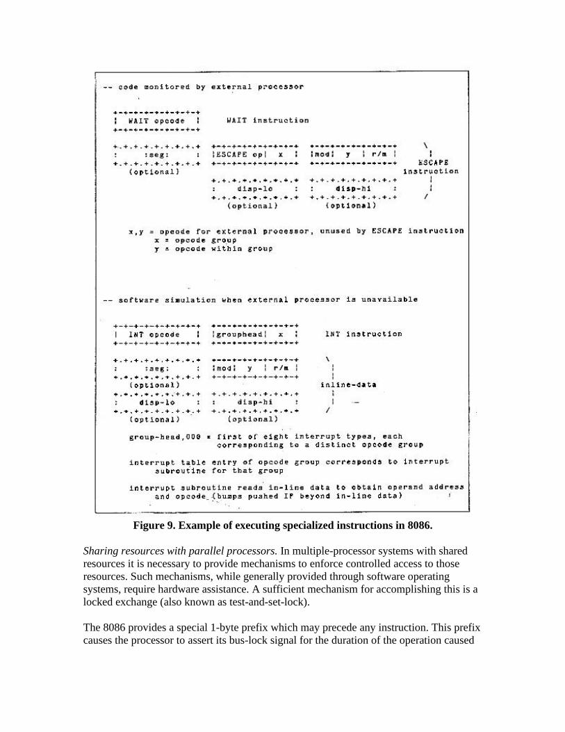
Figure 9. Example of executing specialized instructions in 8086.
Sharing resources with parallel processors. In multiple-processor systems with shared
resources it is necessary to provide mechanisms to enforce controlled access to those
resources. Such mechanisms, while generally provided through software operating
systems, require hardware assistance. A sufficient mechanism for accomplishing this is a
locked exchange (also known as test-and-set-lock).
The 8086 provides a special 1-byte prefix which may precede any instruction. This prefix
causes the processor to assert its bus-lock signal for the duration of the operation caused
by the instruction. It is assumed that external hardware, upon receipt of that signal, will
prohibit bus access for other bus masters during the period of its assertion.
The instruction most useful in this context is an exchange register with memory. A
simple software lock may be implemented with the following code sequences:
Check: MOV AL,1 ;set AL to 1 (implies locked) LOCK XCHG Sema,AL ;test and set lock TEST AL,AL ;set flags based on AL JNZ Check ;retry if lock already set … ;critical region MOV Sema,0 ;clear the lock when done
IX. Summary and Conclusions
"The 8008 begat the 8080, and the 8080 begat the 8085, and the 8085 begat the 8086."
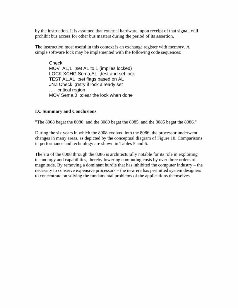
During the six years in which the 8008 evolved into the 8086, the processor underwent
changes in many areas, as depicted by the conceptual diagram of Figure 10. Comparisons
in performance and technology are shown in Tables 5 and 6.
The era of the 8008 through the 8086 is architecturally notable for its role in exploiting
technology and capabilities, thereby lowering computing costs by over three orders of
magnitude. By removing a dominant hurdle that has inhibited the computer industry – the
necessity to conserve expensive processors – the new era has permitted system designers
to concentrate on solving the fundamental problems of the applications themselves.
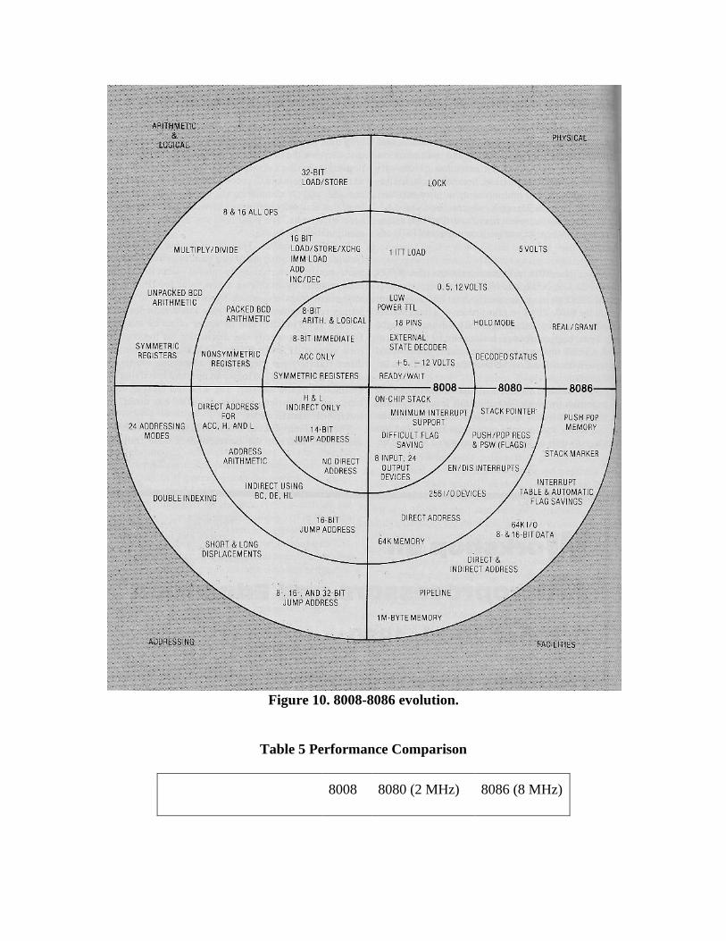
Figure 10. 8008-8086 evolution.
Table 5 Performance Comparison
8008 8080 (2 MHz) 8086 (8 MHz)
register-register transfer 12.5 2 0.25
jump 25 5 0.875
register-immediate
operation
20 3.5 0.5
subroutine call 28 9 2.5
increment (16-bit) 50 2.5 0.25
addition (16-bit) 75 5 0.375
transfer (16-bit) 25 2 0.25
All times are given in microseconds.
Table 6 Technology Comparison
8008 8080 8085 8086
Silicon gate technology P-channel
enhancement
load device
N-channel
enhancement
load device
N-channel
depletion
load device
Scaled N-
channel
(HMOS)
depletion
load device
Clock rate 0.5-0.8 MHz 2-3 MHz 3-5 MHz 5-8 MHz
Min gate delay †
F0 = F1 = 1
30 ns ‡ 15 ns ‡ 5 ns 3 ns
Typical speed- power product 100 pj 40 pj 10 pj 2 pj
Approximate number of
transistors¶
2,000 4,500 6,500 20,000§
Average transistor density
(mil2 per transistor)
8.4 7.5 5.7 2.5
† Fastest inverter function available with worst-case processing.
‡ Linear-mode enhancement load.
§ This is 29,000 transistors if all ROM and PLA available placement sites are counted.
¶ Gate equivalent can be estimates by dividing by 3.
X. Acknowledgments
Many people played significant roles in the development of these processors. Hence, it is
not possible to single out a few for all the credit. However, if forced to choose those
people who played the most significant roles on each chip, we can name the following:
M. E. (Ted) Hoff was the architect and Federico Faggin the chip designer of the 4004.
Stanley Mazor contributed to the 4004 architecture as well as to the architectures of the
8008 and 8080. Hoff and Hal Feeney were the major contributors to the 8008
development. Faggin managed the development of the 8080 and participated in defining
its architecture, with Masatoshi Shima doing the logic and circuit design. Roger
Swanson defined the new instructions for the 8085, while Peter Stoll and Andrew Volk
performed the 8085 logic and circuit design. The 8086 architecture was defined by
Stephen Morse and refined by Bruce Ravenel, with James McKevitt and John Bayliss
responsible for the logic and circuit design. William Pohlman managed both the 8085
and 8086 activities.
The authors thank Stephen Hanna for reviewing this material and providing many helpful
suggestions and comments.
XI. References
Bylinsky, G., "Here Comes the Second Computer Revolution," Fortune, November 1975.
Faggin, F., M. Shima, M. E. Hoff, Jr., H. Feeney, and S. Mazor, "The MCS-4: An LSI
Micro Computer System," IEEE Region 6 Conf. 1972, pp. 8-11.
Hoff, M. E., Jr., "The New LSI Components," 6th Annual IEEE Comp. Soc. Jut. Conf,
1972.
Intel 8080 Microcomputer Systems User's Manual, September 1975.
Intel MCS-8 User's Manual, April 1975
Intel MCS-40 User's Manual, 3d ed., March 1976.
Intel MCS-85 User's Manual, March 1977.
Intel MCS-86 User's Manual, July 1978.
Morse, S. P: "The 8086 Primer," Hayden Book Co., New York, 1980.
Morse, S. P., W. B. Pohlman, and B. W. Ravenel, "The Intel 8086 Micropocessor A 16-
Bit Evolution of the 8080," Computer, June 1978, pp. 18-27.
Shima, M., F. Faggin, and S. Mazor, "An N-Channel 8-Bit Single Chip Microprocessor,"
IEEE Int. Solid-State Circuits Conf, February 1974, pp. 56-57.
Vadasz, L. L., A. S. Grove, T. A. Rowe, and G. E. Moore, "Silicon Gate Technology,"
IEEE Spectrum, October 1969, pp. 27-35.
APPENDIX 1 SAVING AND RESTORING FLAGS IN THE 8008
Interrupt routines must leave all processor flags and registers unaltered so as not to
contaminate the processing that was interrupted. This is most simply done by having the
interrupt routine save all flags and registers on entry and restore them prior to exiting.
The 8008, unlike its successors, has no instruction for directly saving or restoring flags.
Thus 8008 interrupt routines that alter flags (practically every routine does) must
conditionally test each flag to obtain its value and then save that value. Since there are no
instructions for directly setting or clearing flags, the flag values must be restored by
executing code that will put the flags in the saved state.
The 8008 flags can be restored very efficiently if they are saved in the following format
in a byte in memory.
Most significant bit = bit 7
bit 7 = original value of CARRY
bit 6 = original value of SIGN
bit 5 = original value of SIGN
bit 4 = 0
bit 3 = 0
bit 2 = complement of original value of ZERO
bit 1 = complement of original value of ZERO
bit 0 = complement of original value of PARITY
With the information saved in the above format in a byte called FLAGS, the following
two instructions will restore all the saved flag values:
LDA FLAGS ;load saved flags into accumulator ADD A ;add the accumulator to itself
This instruction sequence loads the saved flags into the accumulator and then doubles the
value, thereby moving each bit one position to the left. This causes each flag to be set to
its original value, for the following reasons:
The original value of the CARRY flag, being in the leftmost bit, will be moved out of the
accumulator and wind up in the CARRY flag.
The original value of the SIGN flag, being in bit 6, will wind up in bit 7 and will become
the sign of the result. The new value of the SIGN flag will reflect this sign.
The complement of the original value of the PARITY flag will wind up in bit 1, and it
alone will determine the parity of the result (all other bits in the result are paired up and
have no net effect on parity). The new setting of the PARITY flag will be the
complement of this bit (the flag denotes even parity) and therefore will take on the
original value of the PARITY flag.
Whenever the ZERO flag is 1, the SIGN flag must be 0 (zero is a positive two's-
complement number) and the PARITY flag must be 1 (zero has even parity). Thus an
original ZERO flag value of 1 will cause all bits of FLAGS, with the possible exception
of bit 7, to be 0. After the ADD instruction is executed, all bits of the result will be 0 and
the new value of the ZERO flag will therefore be 1.
An original ZERO flag value of 0 will cause two bits in FLAGS to be 1 and will wind up
in the result as well. The new value of the ZERO flag will therefore be 0.
The above algorithm relies on the fact that flag values are always consistent, i.e., that the
SIGN flag cannot be a 1 when the ZERO flag is a 1. This is always true in the 8008, since
the flags come up in a consistent state whenever the processor is reset and flags can only
be modified by instructions which always leave the flags in a consistent state. The 8080
and its derivatives allow the programmer to modify the flags in an arbitrary manner by
popping a value of his choice off the stack and into the flags. Thus the above algorithm
will not work on those processors.
A code sequence for saving the flags in the required format is as follows:
MVI A,0 ;move zero in accumulator JNC L1 ;jump if CARRY not set ORA 80H ;OR accumulator with 80 hex (set bit 7) L1: JZ L3 ;jump if ZERO set (and SIGN not set and PARITY set) ORA 06H ;OR accumulator with 06 hex (set bits 1 and 2) JM L2 ; jump if negative (SIGN set) ORA 60H ;OR accumulator with 60 hex (set bits 5 and 6) L2: JPE L3 ;jump if parity even (PARITY set) ORA 01H ;OR accumulator with 01 hex (set bit 0) L3: STA FLAGS ;store accumulator in FLAGS
APPENDIX 2 DECIMAL ARITHMETIC
A. Packed BCD
1. Addition. Numbers can be represented as a sequence of decimal digits by using a 4-bit
binary encoding of the digits and packing these encodings two to a byte. Such a
representation is called packed BCD (unpacked BCD would contain only one digit per
byte). In order to preserve this decimal interpretation in performing binary addition on
packed BCD numbers, the value 6 must be added to each digit of the sum whenever (1)
the resulting digit is greater than 9 or (2) a carry occurs out of this digit as a result of the
addition. This is because the 4-bit encoding contains six more combinations than there
are decimal digits. Consider the following examples (numbers are written in hexadecimal
instead of binary for convenience).
Example 1: 81+52
d2 d1 d0 names of digit positions
+
8
5
1
2
packed BCD augend
packed BCD addend
+
D
6
3
adjustment because d1 > 9
1 3 3 packed BCD sum
Example 2: 28+ 19
d2 d1 d0 names of digit positions
+
2
1
8
9
packed BCD augend
packed BCD addend
+
4 1
6
carry occurs out of d0
adjustment for carry
4 7 packed BCD sum
In order to be able to make such adjustments, carries out of either digit position must be
recorded during the addition operation. The 4004, 8080, 8085, and 8086 use the CARRY
and AUXILIARY CARRY flag to record carries out of the leftmost and rightmost digits
respectively. All of these processors provide an instruction for performing the
adjustments. Furthermore, they all contain an add-with-carry instruction to facilitate the
addition of numbers containing more than two digits.
2. Subtraction. Subtraction of packed BCD numbers can be performed in a similar
manner. However, none of the Intel processors prior to the 8086 provides an instruction
for performing decimal adjustment following a subtraction (Zilog's Z-80, introduced two
years before the 8086, also has such an instruction). On processors without the subtract
adjustment instruction, subtraction of packed BCD numbers can be accomplished by
generating the ten's complement of the subtrahend and adding.
3. Multiplication. Multiplication of packed BCD numbers could also be adjusted to give
the correct decimal result if the out-of-digit carries occurring during the multiplication
were recorded. The result of multiplying two one-byte operands is two bytes long (four
digits), and out-of-digit carries can occur on any of the three low-order digits, all of
which would have to be recorded. Furthermore, the carries out of any digit are no longer
restricted to unity, and so counters rather than flags would be required to record the
carries. This is illustrated in the following example (numbers are written in hexadecimal
instead of binary for convenience).
Example 3: 94 * 63
d3 d2 d1 d0 names of digit positions
*
9
6
4
3
packed BCD multiplicand
packed BCD multiplier
3
1
7
B
8
C carry occurs out of d1
carry occurs out of d1, three out of d2
3
+
+
+
9
6
6
6
3
6
6
6
C carry occurs out of d1
adjustment for...
. . .above six...
... carries
4
+
C
6
5
6
C carry occurs out of dl and out of d2
adjustment for above two carries
5
+
2
6
B C carry occurs out of d2
adjustment for above carry
5
+
8 B C
6
adjustment because d0 is greater than 9
5
+
8 C
6
2
adjustment because d1 is greater than 9
5 9 2 2 packed BCD product
The preceding example illustrates two facts. First, packed BCD multiplication
adjustments are possible if the necessary out-of-digit carry information is recorded by the
multiply instruction. Second, the facilities needed in the processor to record this
information and apply the correction are non-trivial.
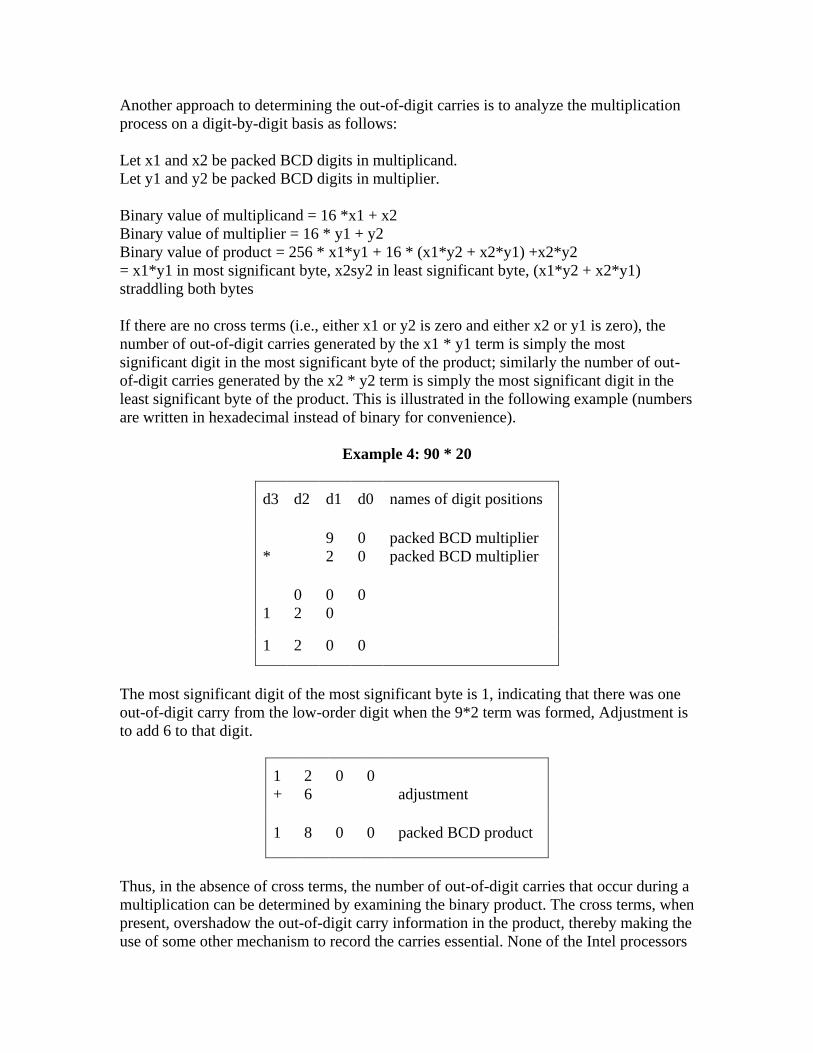
Another approach to determining the out-of-digit carries is to analyze the multiplication
process on a digit-by-digit basis as follows:
Let x1 and x2 be packed BCD digits in multiplicand.
Let y1 and y2 be packed BCD digits in multiplier.
Binary value of multiplicand = 16 *x1 + x2
Binary value of multiplier = 16 * y1 + y2
Binary value of product = 256 * x1*y1 + 16 * (x1*y2 + x2*y1) +x2*y2
= x1*y1 in most significant byte, x2sy2 in least significant byte, (x1*y2 + x2*y1)
straddling both bytes
If there are no cross terms (i.e., either x1 or y2 is zero and either x2 or y1 is zero), the
number of out-of-digit carries generated by the x1 * y1 term is simply the most
significant digit in the most significant byte of the product; similarly the number of out-
of-digit carries generated by the x2 * y2 term is simply the most significant digit in the
least significant byte of the product. This is illustrated in the following example (numbers
are written in hexadecimal instead of binary for convenience).
Example 4: 90 * 20
d3 d2 d1 d0 names of digit positions
*
9
2
0
0
packed BCD multiplier
packed BCD multiplier
1
0
2
0
0
0
1 2 0 0
The most significant digit of the most significant byte is 1, indicating that there was one
out-of-digit carry from the low-order digit when the 9*2 term was formed, Adjustment is
to add 6 to that digit.
1
+
2
6
0 0
adjustment
1 8 0 0 packed BCD product
Thus, in the absence of cross terms, the number of out-of-digit carries that occur during a
multiplication can be determined by examining the binary product. The cross terms, when
present, overshadow the out-of-digit carry information in the product, thereby making the
use of some other mechanism to record the carries essential. None of the Intel processors
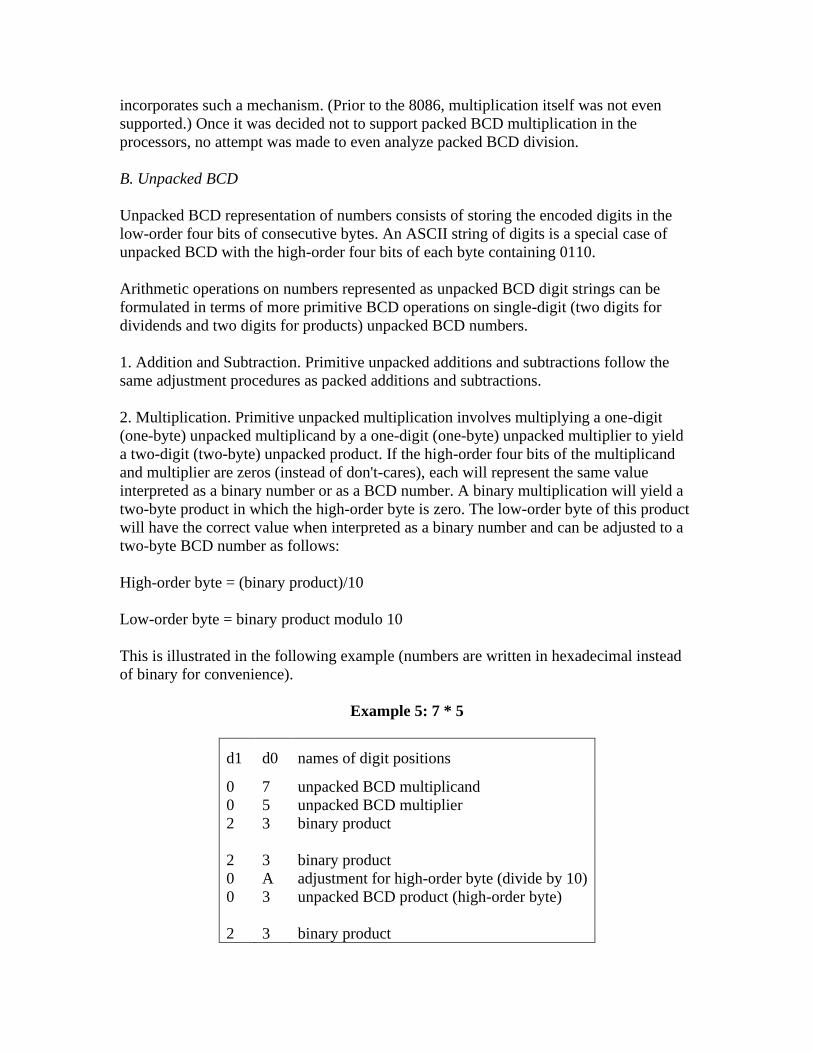
incorporates such a mechanism. (Prior to the 8086, multiplication itself was not even
supported.) Once it was decided not to support packed BCD multiplication in the
processors, no attempt was made to even analyze packed BCD division.
B. Unpacked BCD
Unpacked BCD representation of numbers consists of storing the encoded digits in the
low-order four bits of consecutive bytes. An ASCII string of digits is a special case of
unpacked BCD with the high-order four bits of each byte containing 0110.
Arithmetic operations on numbers represented as unpacked BCD digit strings can be
formulated in terms of more primitive BCD operations on single-digit (two digits for
dividends and two digits for products) unpacked BCD numbers.
1. Addition and Subtraction. Primitive unpacked additions and subtractions follow the
same adjustment procedures as packed additions and subtractions.
2. Multiplication. Primitive unpacked multiplication involves multiplying a one-digit
(one-byte) unpacked multiplicand by a one-digit (one-byte) unpacked multiplier to yield
a two-digit (two-byte) unpacked product. If the high-order four bits of the multiplicand
and multiplier are zeros (instead of don't-cares), each will represent the same value
interpreted as a binary number or as a BCD number. A binary multiplication will yield a
two-byte product in which the high-order byte is zero. The low-order byte of this product
will have the correct value when interpreted as a binary number and can be adjusted to a
two-byte BCD number as follows:
High-order byte = (binary product)/10
Low-order byte = binary product modulo 10
This is illustrated in the following example (numbers are written in hexadecimal instead
of binary for convenience).
Example 5: 7 * 5
d1 d0 names of digit positions
0
0
7
5
unpacked BCD multiplicand
unpacked BCD multiplier
2 3 binary product
2
0
3
A
binary product
adjustment for high-order byte (divide by 10)
0 3 unpacked BCD product (high-order byte)
2 3 binary product
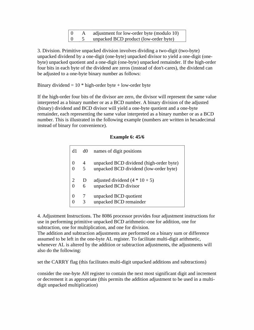
0 A adjustment for low-order byte (modulo 10)
0 5 unpacked BCD product (low-order byte)
3. Division. Primitive unpacked division involves dividing a two-digit (two-byte)
unpacked dividend by a one-digit (one-byte) unpacked divisor to yield a one-digit (one-
byte) unpacked quotient and a one-digit (one-byte) unpacked remainder. If the high-order
four bits in each byte of the dividend are zeros (instead of don't-cares), the dividend can
be adjusted to a one-byte binary number as follows:
Binary dividend = 10 * high-order byte + low-order byte
If the high-order four bits of the divisor are zero, the divisor will represent the same value
interpreted as a binary number or as a BCD number. A binary division of the adjusted
(binary) dividend and BCD divisor will yield a one-byte quotient and a one-byte
remainder, each representing the same value interpreted as a binary number or as a BCD
number. This is illustrated in the following example (numbers are written in hexadecimal
instead of binary for convenience).
Example 6: 45/6
d1 d0 names of digit positions
0
0
2
0
4
5
D
6
unpacked BCD dividend (high-order byte)
unpacked BCD dividend (low-order byte)
adjusted dividend (4 * 10 + 5)
unpacked BCD divisor
0
0
7
3
unpacked BCD quotient
unpacked BCD remainder
4. Adjustment Instructions. The 8086 processor provides four adjustment instructions for
use in performing primitive unpacked BCD arithmetic-one for addition, one for
subtraction, one for multiplication, and one for division.
The addition and subtraction adjustments are performed on a binary sum or difference
assumed to be left in the one-byte AL register. To facilitate multi-digit arithmetic,
whenever AL is altered by the addition or subtraction adjustments, the adjustments will
also do the following:
set the CARRY flag (this facilitates multi-digit unpacked additions and subtractions)
consider the one-byte AH register to contain the next most significant digit and increment
or decrement it as appropriate (this permits the addition adjustment to be used in a multi-
digit unpacked multiplication)
The multiplication adjustment assumes that AL contains a binary product and places the
two-digit unpacked BCD equivalent in AH and AL. The division adjustment assumes that
AH and AL contain a two-digit unpacked BCD dividend and places the binary equivalent
in AH and AL.
The following algorithms show how the adjustment instructions can be used to perform
multi-digit unpacked arithmetic.
Addition
Let augend = a[N] a[N- 1] . . . a[2] a[1]
Let addend = b[N] b[N- 1] . . . b[2] b[1]
Let sum = c[N] c[N-1] . . . c[2] c[1]
0 → (CARRY)
DO i = 1 to N
(a[i]) → (AL)
(AL) + (b[i]) → (AL)
where + denotes add-with-carry
add-adjust (AL) → (AX)
(AL) → (c[i])
Subtraction
Let minuend = a[N] a[N- 1] . . . a[2] a[1]
Let subtrahend = b[N] b[N 1] . . . b[2] bill]
Let difference = c[N] c[N-1] . . . c[2] c[1]
0 → (CARRY)
DO i = 1 to N
(a[i]) → (AL)
(AL) - (b[i]) → (AL)
where - denotes subtract-with-borrow
subtract-adjust (AL) → (AX)
(AL) → (c[i])
Multiplication
Let multiplicand = a[N] a[N- 1] . . . a[2] a[1]
Let multiplier = b
Let product = c[N+ 1] c[N] . . . c[2] c[1]
(b) AND OFH → (b)
0 → (c[1])
DO i = 1 to N
(a[i]) AND OFH → (AL)
(AL) * (b) → (AX)
multiply-adjust (AL) → (AX)
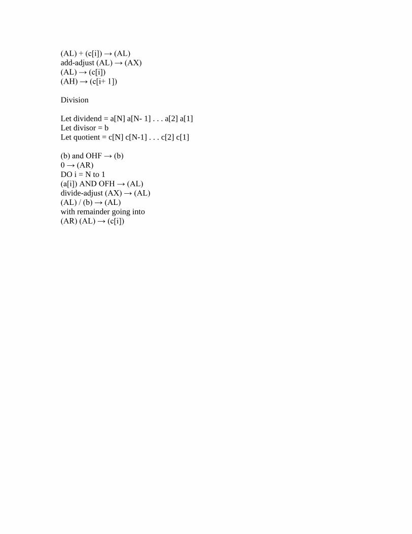
(AL) + (c[i]) → (AL)
add-adjust (AL) → (AX)
(AL) → (c[i])
(AH) → (c[i+ 1])
Division
Let dividend = a[N] a[N- 1] . . . a[2] a[1]
Let divisor = b
Let quotient = c[N] c[N-1] . . . c[2] c[1]
(b) and OHF → (b)
0 → (AR)
DO i = N to 1
(a[i]) AND OFH → (AL)
divide-adjust (AX) → (AL)
(AL) / (b) → (AL)
with remainder going into
(AR) (AL) → (c[i])