Embed Size (px)
Citation preview

January 2017 DocID029728 Rev 1 1/25
www.st.com
AN4909 Application note
Intelligent power switches for 48 V battery applications
Nicolas Aupetit, Alberto Villegas
Introduction For the last 15-20 years, the automotive electronics market has been moving from electromechanical relays to solid state components for driving all kind of loads.
It is obvious why: solid state components are smaller in size, lighter, silent, easy to mass produce because they are housed in SMD packages, and they boast an unrivaled number of switching activations. On top of this, the solutions based on silicon components have a much higher electrical efficiency and offer useful types of diagnostics such as short-circuit, overload and thermal protections, they can supply an actual image of the current flowing into the load, and so on. In fact, they are called “Intelligent Power Switches (IPS)” or “Smart Power MOSFETs” for good reasons. The key “switching” element is an N-MOSFET, with the relevant charge pump. Around the N-MOSFET, logic interfaces and other elements contribute to the protection of the MOS and they generate and manage diagnostic data.
There are two categories of IPS, depending on where the “switch” is placed. If the switch is placed between the load and the ground of the circuit, it is called “low-side.” If the switch is placed between the high voltage and the load (and this is connected directly to the ground), it is a “high-side” configuration. The high-side configuration offers interesting advantages in automotive applications such as high safety, reduction of battery leakage currents, as well as being a real-time (analog) load current mirror.
IPS are available for standard 12 V and 24 V batteries. In the not-too-distant future, high-end diesel and gasoline cars may have two batteries on board: a main battery of “48 V” and a secondary battery of “12 V.” The main interest of the 48 V battery is to support fuel economy and reduce pollutant emissions, especially CO2. The use of a 48 V battery should help to increase a car's efficiency: for example, by using thinner wires in the cars. Actually, if the battery voltage is higher, to drive the same power, the current is lower. A 48 V battery is a good trade-off between safety and functionality.
Several new electronic systems powered by 48 V batteries are already available. More and more often in the future, it will be necessary to have IPS to drive some loads currently driven by the 12 V Smart Power MOSFETs.
Therefore, because of the maximum possible voltage (60 to 70 V) on 48 V batteries, and the spikes generated inside the car, the MOSFET switches will have to withstand voltages in the order of 80 V at 25 °C.
Today the number of Smart Power MOSFETs or IPS able to comply with these requirements is extremely low and they are expensive.
In this application note, we demonstrate a way to design circuits able to drive all kinds of loads with components already in mass production, that are AEC-Q100 or AEC-Q101 qualified, and that offer functionalities similar to those of the 12 V or 24 V IPS available in the market today.

Contents AN4909
2/25 DocID029728 Rev 1
Contents
1 General overview ............................................................................. 3
2 Schematic and description ............................................................. 4
3 Shunt resistance of 4 mΩ ............................................................... 5
4 Current sensing ............................................................................... 6
5 Power NMOS transistor .................................................................. 8
5.1 Conduction losses ............................................................................. 8
5.2 Switching losses ................................................................................ 8
5.3 Current flowing into the gate (Idriver) ................................................ 9
5.4 Junction temperature ...................................................................... 10
6 Overcurrent protection ................................................................. 12
6.1 OCP timing ...................................................................................... 13
7 Gate driver ..................................................................................... 16
7.1 SD /OD pin ............................................................................................ 17
8 Temperature sensor ...................................................................... 18
9 Free wheeling diode ...................................................................... 19
10 Microcontroller .............................................................................. 21
11 Application board .......................................................................... 22
12 Conclusion ..................................................................................... 23
13 Revision history ............................................................................ 24

AN4909 General overview
DocID029728 Rev 1 3/25
1 General overview Figure 1: General system overview
IPS for 48 V applications are intended to drive resistive or inductive loads with one side connected to ground.
This application board performs an analog current measurement through a shunt resistance, which delivers a voltage proportional to the load current. This current information is analyzed by a microcontroller (MCU) and displayed in real time on the screen.
Overcurrent protection is also available on this board, and the application latches off in case of overload. This information is treated by the MCU and only a hardware push button can unlatch the device.
In the particular case of this application board, a thermal sensor is used to control the MOS temperature, when it goes beyond 125 °C, to protect the PCB. The temperature information is analyzed by the MCU which displays the temperature in real time on a supervising screen and can switch off the application if it is overheating.
The MCU generates a configurable PWM to drive the gate of the power NMOS.
GateDriver
12V 48V
Load
Overcurrent protection
Mic
rocon
trolle
r
3.6V
RshuntCurrentsensing
ThermalSensorPower
NMOS
Freewheel Diode

Schematic and description AN4909
4/25 DocID029728 Rev 1
2 Schematic and description
Eight ICs are used in this application board: “Smart power MOS similar function”. Except for the temperature probe and the MCU, all the components used in this application are automotive grade qualified.
Figure 2: Schematic
8
9
10
7
1
2
3
4
5
6
J1
13
12
11
10
96
5
4
3
2
1 14
VSS
VDD
VSS
VDD
HE
10
_2X
5P
TS
3
2
1
2
1
6
10
9
8
2
1
1
2
10987654321
87
8
6
54
3
2
1
1 2
714
3
4
5
6
7
11
12
13
1
SD_LATCH
OUT
SD
GND_3
GND_2
GND_1
I_SENSE
HIN
D1
R3
R11
Q1
5
4 3
2
1
R15
CC1
R17
R10
D2
C12
R9
R7
C13
R12
U4
R2 R6
C5
5
C8
R13
C2
R16
1
7
6
3
C18
C1
C3
C7
C6
R1
D3
R14
C19
R4
R5 5
2
1
C10
C9
C11
C14
C15
C16
C17
V1
24
R8
C4
CC6
CC5
CC4
CC3
CC2
Q2
U3
B2
B1
U2
U1
S1
Gate driver
Freewheel diode
NMOS
Current sensor
Overcurrent protect ion
Temperature sensor
Via m icrocont roller

AN4909 Shunt resistance of 4 mΩ
DocID029728 Rev 1 5/25
3 Shunt resistance of 4 mΩ
The current flowing into the load is measured by a high-side current sensor (TSC1031IYDT/PT) and a shunt resistor (Rshunt = S1 in Figure 2). In the current application, the 48 V battery is able to deliver a maximum current of 15 A. To limit high power dissipation into the shunt, this current should be as low as possible.
A full measurement range is considered on the output of the TSC1031 (from GND to 3 V). Note that the range from 3.0 V to 3.6 V is used to detect overload and activate the overcurrent protection.
The Rshunt resistor value can be chosen using Equation 1.
Equation 1
As the gain of the TSC1031 is set to 50 V/V, the Rshunt value is 4 mΩ. We can therefore expect a maximum power dissipation in the Rshunt of 4 mΩ *15 A2 = 900 mW.
To optimize precision, the chosen Rshunt has a 4 terminal design, which allows resistance precision in the range 0.5 % to 1 %. An example of such a resistor is the Vishay Dale WSL3637.

Current sensing AN4909
6/25 DocID029728 Rev 1
4 Current sensing
The current sensing measurement is extremely important. Firstly, to control the current flowing into the load and secondly to be able to make a decision if a default event occurs like a short circuit or an over-current event. The current sensing measurement is made using the high-side current sensor, TSC1031IYDT/PT. In this device, the input common-mode voltage and the power supply are independent. Although the TSC1031 can be powered with a voltage range of 2.7 V to 5.5 V, the input common-mode voltage can range from 2.9 V to 70 V. This allows the TSC1031 to support the load dump which is possible with 48 V batteries.
The TSC1031 has a selectable pin (SEL) which allows a gain of 50 V/V (SEL = GND) or 100 V/V (SEL = Vcc). As shown in Figure 2, the gain is set with an I/O of the MCU.
The high-side current sensor provides an output voltage proportional to the current flowing into the Rshunt. Ideally, the current sensing output voltage should be equal to the input differential voltage, Vsense, multiplied by the gain. Actually, it is slightly different, mainly due to the combined error of the input voltage offset of the TSC1031 and its gain accuracy.
Figure 3 shows the maximum guaranteed error which can occur on the output of the TSC1031 at 25 °C, and over its temperature operative range.
Figure 3: Maximum output voltage error of the TSC1031
-25
-20
-15
-10
-5
0
5
10
15
20
25
5 15 25 35 45 55 65 75 85 95
∆V
ou
t (%
)
VSense (mV)
Guaranteed accuracyover temperature
Guaranteed accuracy@25°C
AN4909 Current sensing
DocID029728 Rev 1 7/25
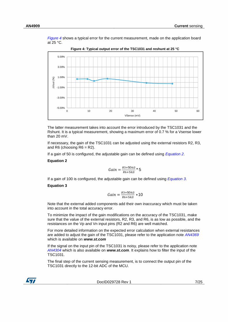
Figure 4 shows a typical error for the current measurement, made on the application board at 25 °C.
Figure 4: Typical output error of the TSC1031 and reshunt at 25 °C
The latter measurement takes into account the error introduced by the TSC1031 and the Rshunt. It is a typical measurement, showing a maximum error of 0.7 % for a Vsense lower than 20 mV.
If necessary, the gain of the TSC1031 can be adjusted using the external resistors R2, R3, and R6 (choosing R6 = R2).
If a gain of 50 is configured, the adjustable gain can be defined using Equation 2.
Equation 2
If a gain of 100 is configured, the adjustable gain can be defined using Equation 3.
Equation 3
Note that the external added components add their own inaccuracy which must be taken into account in the total accuracy error.
To minimize the impact of the gain modifications on the accuracy of the TSC1031, make sure that the value of the external resistors, R2, R3, and R6, is as low as possible, and the resistances on the Vp and Vn input pins (R2 and R6) are well matched.
For more detailed information on the expected error calculation when external resistances are added to adjust the gain of the TSC1031, please refer to the application note AN4369 which is available on www.st.com
If the signal on the input pin of the TSC1031 is noisy, please refer to the application note AN4304 which is also available on www.st.com. It explains how to filter the input of the TSC1031.
The final step of the current sensing measurement, is to connect the output pin of the TSC1031 directly to the 12-bit ADC of the MCU.
-5.00%
-3.00%
-1.00%
1.00%
3.00%
5.00%
0 10 20 30 40 50 60
∆V
ou
t (%
)
VSense (mV)
505
5010*

Power NMOS transistor AN4909
8/25 DocID029728 Rev 1
5 Power NMOS transistor
The power NMOS is a key function in the current application. It helps control the current into the load and also serves to protect the application when a fault appears. It must sustain a voltage greater than 48 V as it must also withstand load dump. In addition, to limit power dissipation, the Rdson must be as low as possible.
The STH275N8F7-6AG is an N-channel 80 V with an Rdson max of 2.1 mΩ at 25 °C. It is designed for automotive applications and is AEC-Q101 qualified.
The NMOS is driven by the gate driver L6491 which is PWM controlled by the MCU. In this application, the PWM frequency can be configured in the range 250 Hz to 20 kHz. Nevertheless, by working at higher frequencies it increases the switching losses leading to an increase of the junction temperature of the NMOS.
The equations in the following sections 5.1, 5.2, 5.3, and 5.4 show the NMOS losses and junction temperature behavior.
5.1 Conduction losses
Equation 4 is used to calculate the conduction losses.
Equation 4
In this application:
Rdson = 2.1 mΩ
Id = the current flowing through the NMOS, 15 A
Vout/Vin represents the duty cycle of the PWM at 50 %
In this case, the conduction losses are 236 mW.
5.2 Switching losses
The switching interval begins when the L6491 gate driver turns-on and begins to inject current into the NMOS gate to charge its input capacitance. The switching losses can be calculated using Equation 5.
Equation 5
In this application:
VH: high voltage = 48 V
Id: the current flowing through the NMOS = 15 A
f: switching frequency = 500 Hz
tr and tf represent the timing needed to switch the MOS ON/OFF or OFF/ON and can be calculated using Equation 6
Equation 6
=

AN4909 Power NMOS transistor
DocID029728 Rev 1 9/25
Where Qg represents the NMOS gate charge to move through the switching interval and can be approximated using Equation 7.
Equation 7
Where Qgd is the gate–drain charge of the NMOS and Qgs is the gate–source charge of the NMOS, the values being which is 46 nC and 96 nC respectively.
5.3 Current flowing into the gate (Idriver)
As there is a special path for the rising time (L-H) through the 33 Ω resistor and another path for the falling time (H-L) through the parallel resistors, 33 Ω and 10 Ω respectively, the Idriver is different for each edge. It can be calculated using Equation 8 (L-H) and Equation 9 (H-L).
Equation 8
Equation 9
With Vdd, the voltage drive of the gate driver L6491 is 12 V
Gm, the transconductance of the NMOS, is 175 A/V
Vth, the typical gate threshold voltage, is 3 V
Rgate L_H is 33 Ω
Rgate H_L is 33 Ω//10 Ω = 7.7 Ω
In this case, the switching losses can be considered as indicated in the following equation:
Where Ps = 105 mW.
2
( ) =)h+
( ) =h+
Power NMOS transistor AN4909
10/25 DocID029728 Rev 1
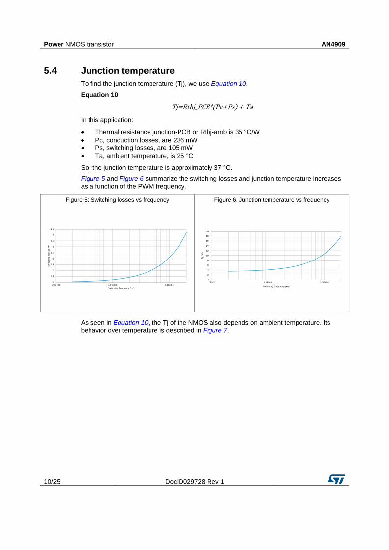
5.4 Junction temperature
To find the junction temperature (Tj), we use Equation 10.
Equation 10
In this application:
Thermal resistance junction-PCB or Rthj-amb is 35 °C/W
Pc, conduction losses, are 236 mW
Ps, switching losses, are 105 mW
Ta, ambient temperature, is 25 °C
So, the junction temperature is approximately 37 °C.
Figure 5 and Figure 6 summarize the switching losses and junction temperature increases as a function of the PWM frequency.
Figure 5: Switching losses vs frequency
Figure 6: Junction temperature vs frequency
As seen in Equation 10, the Tj of the NMOS also depends on ambient temperature. Its behavior over temperature is described in Figure 7.
0
0.5
1
1.5
2
2.5
3
3.5
4
4.5
1.0E+02 1.0E+03 1.0E+04
sw
tich
ing
lo
ss
es
(W)
Switching frequency (Hz)
0
20
40
60
80
100
120
140
160
180
200
1.0E+02 1.0E+03 1.0E+04
Tj (°
C)
Switching frequency (Hz)

AN4909 Power NMOS transistor
DocID029728 Rev 1 11/25
Figure 7: Junction temperature vs. ambient temperature
We recommend working with low frequency PWMs to avoid overheating the NMOS and to reduce any possible EMI issues.
-40
-20
0
20
40
60
80
100
120
140
160
-40 -20 0 20 40 60 80 100 120
Tj (°
C)
Ambient temperature (°C)
PWM @ 500 Hz-50%
Overcurrent protection AN4909
12/25 DocID029728 Rev 1
6 Overcurrent protection
When a short circuit or overcurrent occurs, the application must be switched off as quickly as possible. Moreover, after such events, the application must not restart by itself and must stay switched off until a manual reload is applied. The TS3021Y is a high speed comparator, which combined with the D flip-flop (HCF4013), is used to execute a latch function in case of an overcurrent event. Both devices are qualified and characterized according to AEC-Q100 and Q003.
The output full range of the current sensor TSC1031 is from GND to 3 V for the current measurement. As the Vcc of the application is 3.6 V, a 0.6 V range exists, from 3 V to 3.6 V, which is used to detect overcurrent.
The comparator TS3021 is used to detect overcurrent events. When the output of the current sensor goes beyond the reference of the comparator, the latter changes its state. To avoid any incorrect information, the reference of the comparator is set at 3.3 V which is slightly above the maximum output swing of the current sensor. This is done with the resistor divider bridge (R4, R5) and is applied on the pin of the comparator. So in normal use, the output of the comparator is set to GND.
If an overcurrent occurs, the output of the current sensor will rise above the 3.3 V and so the output of the comparator will change from a low state to a high state (3.6 V).
This information is directly latched because of the D flip-flop. In addition, after such an
event, the output of the HCF4013 ( Q1 ) changes from a high state to a low state. The
Q1 pin is connected to the gate driver L6491 and until this pin goes into a low state, the
gate driver switches-off the NMOS.
The Q1 pin is also supervised by a GPIO of the MCU which can be informed if an
overcurrent event occurs. In this case, after an overcurrent default, the MCU is able to display an alert directly on screen.
To restart the application and unlatch the D flip-flop, a clock signal must be applied on pin CLOCK1 of the HCF4013. This operation is realized by a push button controlled by the MCU.
Note at startup, a clock signal is applied on the pin CLOCK1 by the MCU to launch the application.
AN4909 Overcurrent protection
DocID029728 Rev 1 13/25
6.1 OCP timing
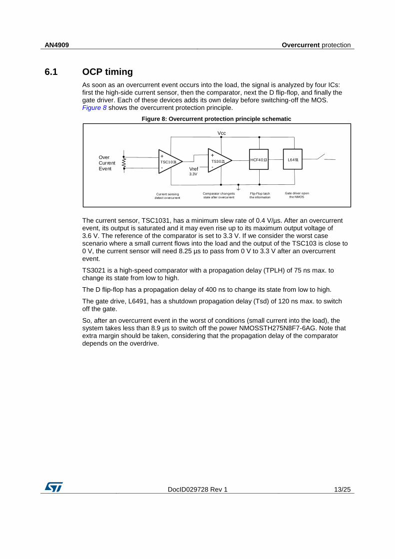
As soon as an overcurrent event occurs into the load, the signal is analyzed by four ICs: first the high-side current sensor, then the comparator, next the D flip-flop, and finally the gate driver. Each of these devices adds its own delay before switching-off the MOS. Figure 8 shows the overcurrent protection principle.
Figure 8: Overcurrent protection principle schematic
The current sensor, TSC1031, has a minimum slew rate of 0.4 V/µs. After an overcurrent event, its output is saturated and it may even rise up to its maximum output voltage of 3.6 V. The reference of the comparator is set to 3.3 V. If we consider the worst case scenario where a small current flows into the load and the output of the TSC103 is close to 0 V, the current sensor will need 8.25 µs to pass from 0 V to 3.3 V after an overcurrent event.
TS3021 is a high-speed comparator with a propagation delay (TPLH) of 75 ns max. to change its state from low to high.
The D flip-flop has a propagation delay of 400 ns to change its state from low to high.
The gate drive, L6491, has a shutdown propagation delay (Tsd) of 120 ns max. to switch off the gate.
So, after an overcurrent event in the worst of conditions (small current into the load), the system takes less than 8.9 µs to switch off the power NMOSSTH275N8F7-6AG. Note that extra margin should be taken, considering that the propagation delay of the comparator depends on the overdrive.
+
-
OverCurrentEvent
+
-
Vcc
TSC1031 TS3021
Vref3.3V
HCF4013 L6491
Current sensingdetect overcurrent
Comparator changeitsstate after overcurrent
Flip-Flop latchthe information
Gate driver openthe NMOS
Overcurrent protection AN4909
14/25 DocID029728 Rev 1
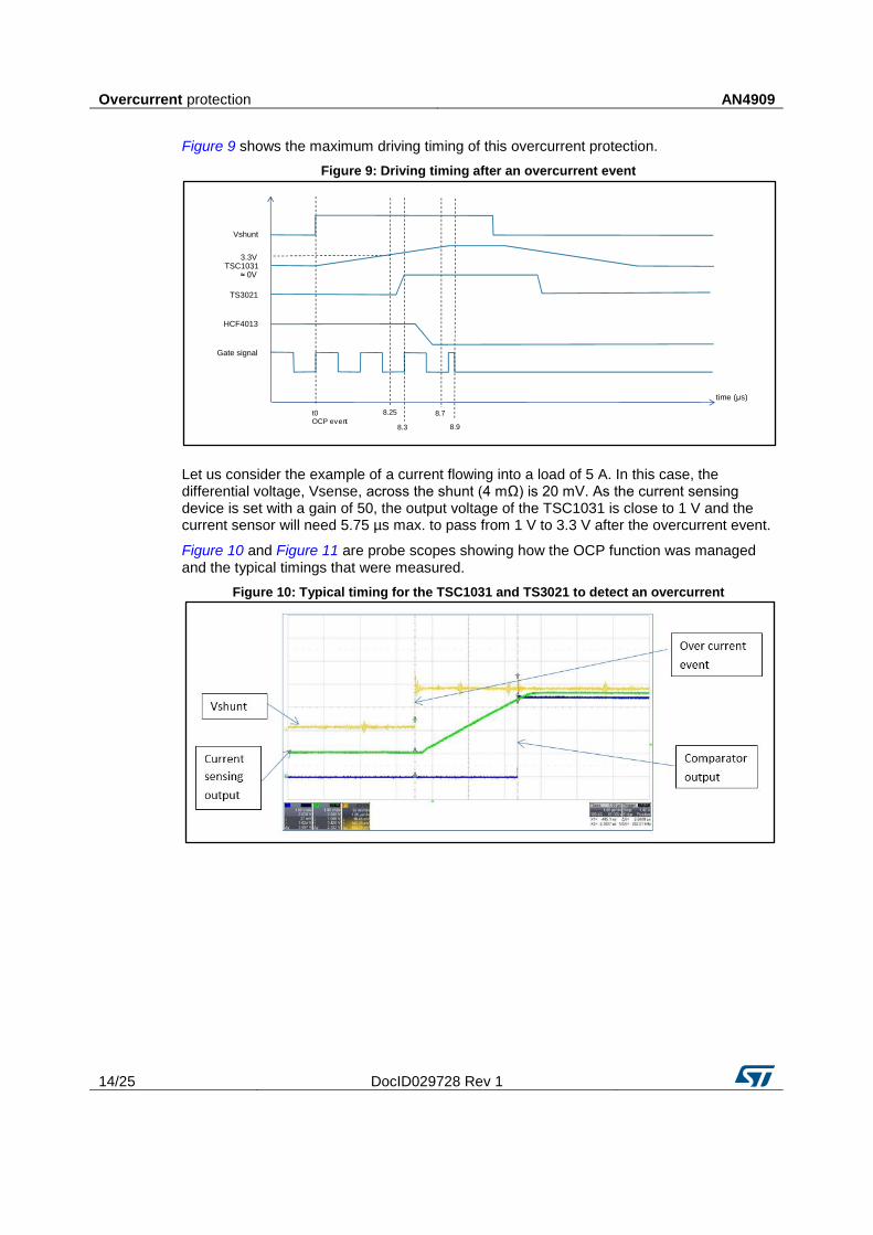
Figure 9 shows the maximum driving timing of this overcurrent protection.
Figure 9: Driving timing after an overcurrent event
Let us consider the example of a current flowing into a load of 5 A. In this case, the differential voltage, Vsense, across the shunt (4 mΩ) is 20 mV. As the current sensing device is set with a gain of 50, the output voltage of the TSC1031 is close to 1 V and the current sensor will need 5.75 µs max. to pass from 1 V to 3.3 V after the overcurrent event.
Figure 10 and Figure 11 are probe scopes showing how the OCP function was managed and the typical timings that were measured.
Figure 10: Typical timing for the TSC1031 and TS3021 to detect an overcurrent
time (µs)
8.25
8.3 8.9
8.7t0OCP event
TSC1031
TS3021
3.3V
Vshunt
≈ 0V
HCF4013
Gate signal

AN4909 Overcurrent protection
DocID029728 Rev 1 15/25
Figure 11: Typical timing for the HCF4013 and L6491 after an overcurrent event
In this example, when an overcurrent event occurs on the shunt resistor, it needs 2.9 µs for the output of the comparator to change its state. As seen in the theoretical calculations, this timing is mainly due to the slew rate of the high-side current sensor, TSC1031.
As soon as the TS3021 changes its state, it needs 240 ns for the D flip-flop to latch. 100 ns later, the gate driver is switched off and an additional 350 ns are needed to completely switch off the power NMOS.
In Figure 11 (tested with HV = 15 V), we can see that once the D flip-flop latches, even if the comparator goes into a low state, a normal current flows though the shunt and the power NMOS is still switched-off. Only a clock signal on the pin CLOCK1 can unlatch the D flip-flop and restart the application.
So, from a typical measurement, as soon as there is an overcurrent event in the load, it takes roughly 3.6 µs to switch off the power NMOS.
In the above case, the OCP function was tested using a resistive load. If an LC load is used, there is a risk of current ringing into the shunt during the switching phase. Such ringing may activate the comparator and thus the OCP function. In this situation, a blanking period is necessary before latching the D flip-flop.
Gate driver AN4909
16/25 DocID029728 Rev 1
7 Gate driver
The current into the load is set by a PWM signal and a gate driver is needed to drive the NMOS correctly with respect to this signal. The L6491 (A6491DTR for the AEC-Q100 version) is a single-chip, half-bridge gate driver for an N-channel power MOSFET. The high-side section is designed to withstand a voltage rail up to 600 V. The logic inputs are CMOS/TTL which are compatible down to 3.3 V. This allows for easy interfacing with the STM8L MCU.
To choose the appropriate Cboot value, the power NMOS can be seen as an equivalent capacitor, Cext, which can be calculated as described in Equation 11.
Equation 11
In this application, the total gate charge of the NMOS, Qgate, is 193 nC and the Vgate is 10 V. Therefore, Cext is roughly equal to 20 nF. The ratio between Cext and Cboot is proportional to the cyclical voltage loss. Cboot must be much greater than Cext. So, Cboot = 2.2 µF.
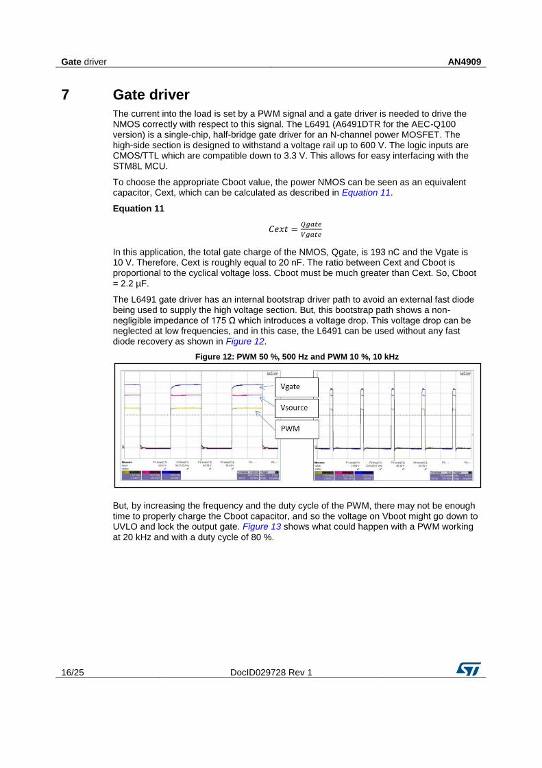
The L6491 gate driver has an internal bootstrap driver path to avoid an external fast diode being used to supply the high voltage section. But, this bootstrap path shows a non-negligible impedance of 175 Ω which introduces a voltage drop. This voltage drop can be neglected at low frequencies, and in this case, the L6491 can be used without any fast diode recovery as shown in Figure 12.
Figure 12: PWM 50 %, 500 Hz and PWM 10 %, 10 kHz
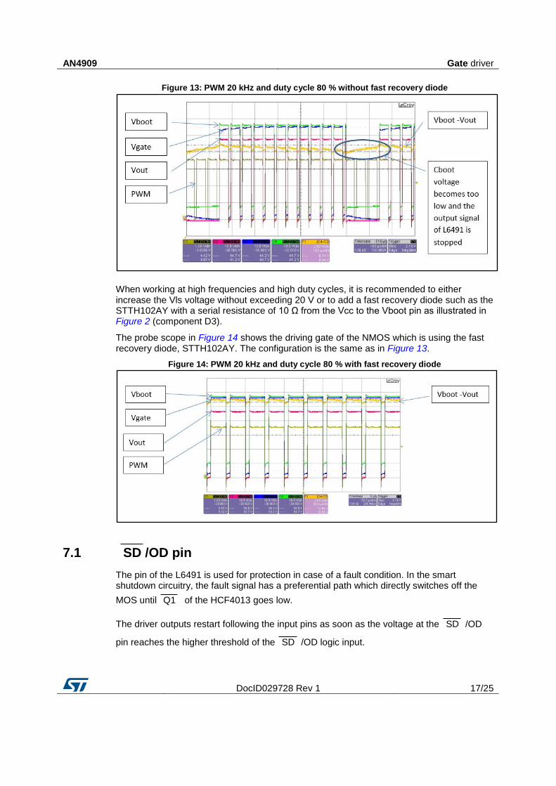
But, by increasing the frequency and the duty cycle of the PWM, there may not be enough time to properly charge the Cboot capacitor, and so the voltage on Vboot might go down to UVLO and lock the output gate. Figure 13 shows what could happen with a PWM working at 20 kHz and with a duty cycle of 80 %.
AN4909 Gate driver
DocID029728 Rev 1 17/25
Figure 13: PWM 20 kHz and duty cycle 80 % without fast recovery diode
When working at high frequencies and high duty cycles, it is recommended to either increase the Vls voltage without exceeding 20 V or to add a fast recovery diode such as the STTH102AY with a serial resistance of 10 Ω from the Vcc to the Vboot pin as illustrated in Figure 2 (component D3).
The probe scope in Figure 14 shows the driving gate of the NMOS which is using the fast recovery diode, STTH102AY. The configuration is the same as in Figure 13.
Figure 14: PWM 20 kHz and duty cycle 80 % with fast recovery diode
7.1 SD /OD pin
The pin of the L6491 is used for protection in case of a fault condition. In the smart shutdown circuitry, the fault signal has a preferential path which directly switches off the
MOS until Q1 of the HCF4013 goes low.
The driver outputs restart following the input pins as soon as the voltage at the SD /OD
pin reaches the higher threshold of the SD /OD logic input.

Temperature sensor AN4909
18/25 DocID029728 Rev 1
8 Temperature sensor
High current flows through the MOS and depending on the PWM frequency (see Section 5: "Power NMOS transistor") the NMOS may reach a dangerous temperature. So, it is important to control the temperature to protect the application. The PCB temperature elevation is measured with a thermal probe. The STTS751 is a digital temperature sensor, which communicates over a 2-wire SMBus 2.0 compatible bus. The temperature is measured with a user-configurable resolution between 9 and 12 bits. At 9 bits, the smallest step size is 0.5 °C, and at 12 bits, it is 0.0625 °C. The open-drain EVENT output is used to indicate an alarm condition i.e. to see if the measured temperature has exceeded the user-programmed high limit or fallen below the low limit. When the EVENT pin is asserted, the host can respond using the SMBus alert response.
AN4909 Free wheeling diode
DocID029728 Rev 1 19/25
9 Free wheeling diode
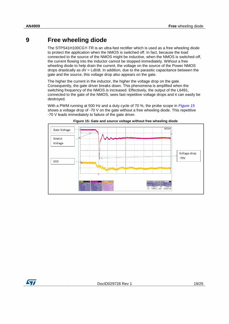
The STPS41H100CGY-TR is an ultra-fast rectifier which is used as a free wheeling diode to protect the application when the NMOS is switched off. In fact, because the load connected to the source of the NMOS might be inductive, when the NMOS is switched-off, the current flowing into the inductor cannot be stopped immediately. Without a free wheeling diode to help drain the current, the voltage on the source of the Power NMOS drops drastically as dV = LdI/dt. In addition, due to the parasitic capacitance between the gate and the source, this voltage drop also appears on the gate.
The higher the current in the inductor, the higher the voltage drop on the gate. Consequently, the gate driver breaks down. This phenomena is amplified when the switching frequency of the NMOS is increased. Effectively, the output of the L6491, connected to the gate of the NMOS, sees fast repetitive voltage drops and it can easily be destroyed.
With a PWM running at 500 Hz and a duty cycle of 70 %, the probe scope in Figure 15 shows a voltage drop of -70 V on the gate without a free wheeling diode. This repetitive -70 V leads immediately to failure of the gate driver.
Figure 15: Gate and source voltage without free wheeling diode
Free wheeling diode AN4909
20/25 DocID029728 Rev 1
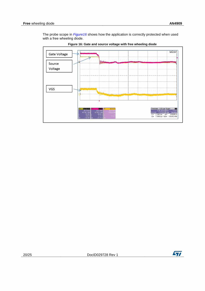
The probe scope in Figure16 shows how the application is correctly protected when used with a free wheeling diode.
Figure 16: Gate and source voltage with free wheeling diode

AN4909 Microcontroller
DocID029728 Rev 1 21/25
10 Microcontroller
The STM8L151 is an ultra low-power 8 bit MCU, powered with Vcc = 3.6 V.
The MCU is mainly used to drive the application and display information about the whole system as follows:
It generates the PWM signal to switch off or switch on the power N-MOS with a dedicated embedded timer.
It is able to read and analyze data coming from the output of the current sensor with a 12 bit ADC. It then displays on a screen the value of the current flowing into the load.
It is able to read and display the value coming from the digital temperature sensor (due to the SMBus). It then displays the value of the temperature of the MOS on a screen. It is also able to prevent over temperature with a dedicated pin.
It is able to give information about overload with its dedicated I/O and can reset the latch to restart the application after an OCP event.
Application board AN4909
22/25 DocID029728 Rev 1
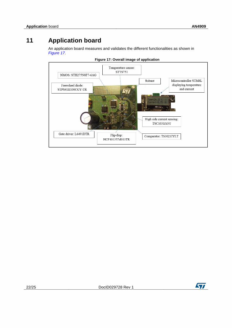
11 Application board
An application board measures and validates the different functionalities as shown in Figure 17.
Figure 17: Overall image of application

AN4909 Conclusion
DocID029728 Rev 1 23/25
12 Conclusion
We have explained how to build and configure a smart switch for a 48 V battery application with the available devices on the market. For this very useful circuit, we have also described:
One possible architecture
Component selection
Schematic
Performance measurements

Revision history AN4909
24/25 DocID029728 Rev 1
13 Revision history Table 1: Document revision history
Date Revision Changes
27-Jan-2017 1 Initial release
AN4909
DocID029728 Rev 1 25/25
IMPORTANT NOTICE – PLEASE READ CAREFULLY
STMicroelectronics NV and its subsidiaries (“ST”) reserve the right to make changes, corrections, enhancements, modifications, and improvements to ST products and/or to this document at any time without notice. Purchasers should obtain the latest relevant information on ST products before placing orders. ST products are sold pursuant to ST’s terms and conditions of sale in place at the time of order acknowledgement.
Purchasers are solely responsible for the choice, selection, and use of ST products and ST assumes no liability for application assistance or the design of Purchasers’ products.
No license, express or implied, to any intellectual property right is granted by ST herein.
Resale of ST products with provisions different from the information set forth herein shall void any warranty granted by ST for such product.
ST and the ST logo are trademarks of ST. All other product or service names are the property of their respective owners.
Information in this document supersedes and replaces information previously supplied in any prior versions of this document.
© 2017 STMicroelectronics – All rights reserved