Embed Size (px)
Citation preview
Inter-Chip Supplement to the USB Revision 3.0 Specification
Revision 1.02
May 19, 2014
Inter-Chip Supplement to the USB Revision 3.0 Specification
ii
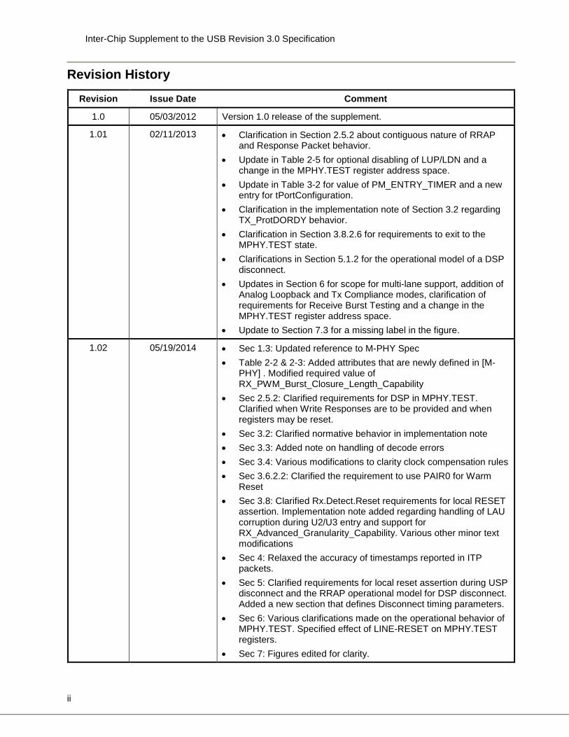
Revision History
Revision Issue Date Comment
1.0 05/03/2012 Version 1.0 release of the supplement.
1.01 02/11/2013 • Clarification in Section 2.5.2 about contiguous nature of RRAP and Response Packet behavior.
• Update in Table 2-5 for optional disabling of LUP/LDN and a change in the MPHY.TEST register address space.
• Update in Table 3-2 for value of PM_ENTRY_TIMER and a new entry for tPortConfiguration.
• Clarification in the implementation note of Section 3.2 regarding TX_ProtDORDY behavior.
• Clarification in Section 3.8.2.6 for requirements to exit to the MPHY.TEST state.
• Clarifications in Section 5.1.2 for the operational model of a DSP disconnect.
• Updates in Section 6 for scope for multi-lane support, addition of Analog Loopback and Tx Compliance modes, clarification of requirements for Receive Burst Testing and a change in the MPHY.TEST register address space.
• Update to Section 7.3 for a missing label in the figure.
1.02 05/19/2014 • Sec 1.3: Updated reference to M-PHY Spec • Table 2-2 & 2-3: Added attributes that are newly defined in [M-
PHY] . Modified required value of RX_PWM_Burst_Closure_Length_Capability
• Sec 2.5.2: Clarified requirements for DSP in MPHY.TEST. Clarified when Write Responses are to be provided and when registers may be reset.
• Sec 3.2: Clarified normative behavior in implementation note • Sec 3.3: Added note on handling of decode errors • Sec 3.4: Various modifications to clarity clock compensation rules • Sec 3.6.2.2: Clarified the requirement to use PAIR0 for Warm
Reset • Sec 3.8: Clarified Rx.Detect.Reset requirements for local RESET
assertion. Implementation note added regarding handling of LAU corruption during U2/U3 entry and support for RX_Advanced_Granularity_Capability. Various other minor text modifications
• Sec 4: Relaxed the accuracy of timestamps reported in ITP packets.
• Sec 5: Clarified requirements for local reset assertion during USP disconnect and the RRAP operational model for DSP disconnect. Added a new section that defines Disconnect timing parameters.
• Sec 6: Various clarifications made on the operational behavior of MPHY.TEST. Specified effect of LINE-RESET on MPHY.TEST registers.
• Sec 7: Figures edited for clarity.
Inter-Chip Supplement to the USB Revision 3.0 Specification
iii
Universal Serial Bus Specification Supplement Copyright © 2014, Texas Instruments, Hewlett-Packard Company, Intel Corporation, Microsoft
Corporation, Renesas Corporation, ST-Ericsson.
All rights reserved
INTELLECTUAL PROPERTY DISCLAIMER
THIS SPECIFICATION IS PROVIDED TO YOU “AS IS” WITH NO WARRANTIES WHATSOEVER, INCLUDING ANY WARRANTY OF MERCHANTABILITY, NON-INFRINGEMENT, OR FITNESS FOR ANY PARTICULAR PURPOSE. THE AUTHORS OF THIS SPECIFICATION DISCLAIM ALL LIABILITY, INCLUDING LIABILITY FOR INFRINGEMENT OF ANY PROPRIETARY RIGHTS, RELATING TO USE OR IMPLEMENTATION OF INFORMATION IN THIS SPECIFICATION. THE PROVISION OF THIS SPECIFICATION TO YOU DOES NOT PROVIDE YOU WITH ANY LICENSE, EXPRESS OR IMPLIED, BY ESTOPPEL OR OTHERWISE, TO ANY INTELLECTUAL PROPERTY RIGHTS. All product names are trademarks, registered trademarks, or servicemarks of their respective owners.
Inter-Chip Supplement to the USB Revision 3.0 Specification
iv
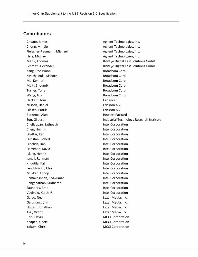
Contributors
Choate, James Agilent Technologies, Inc. Chong, Min Jie Agilent Technologies, Inc. Fleischer-Reumann, Michael Agilent Technologies, Inc. Herz, Michael Agilent Technologies, Inc. Marik, Thomas BitifEye Digital Test Solutions GmbH Schmitt, Alexander BitifEye Digital Test Solutions GmbH Kang, Dae Woon Broadcom Corp. Kasichainula, Kishore Broadcom Corp. Ma, Kenneth Broadcom Corp. Maiti, Shoumik Broadcom Corp. Turner, Tony Broadcom Corp. Wang, Jing Broadcom Corp. Hackett, Tom Cadence Nilsson, Daniel Ericsson AB Olesen, Patrik Ericsson AB Berkema, Alan Hewlett Packard Sun, Gilbert Industrial Technology Research Institute Chellappan, Satheesh Intel Corporation Chen, Huimin Intel Corporation Drottar, Ken Intel Corporation Dunstan, Robert Intel Corporation Froelich, Dan Intel Corporation Harriman, David Intel Corporation Icking, Henrik Intel Corporation Ismail, Rahman Intel Corporation Knuutila, Kai Intel Corporation Leucht-Roth, Ulrich Intel Corporation Mukker, Anoop Intel Corporation Ramakrishnan, Sivakumar Intel Corporation Ranganathan, Sridharan Intel Corporation Saunders, Brad Intel Corporation Vadivelu, Karthi R Intel Corporation Galbo, Neal Lexar Media, Inc. Geldman, John Lexar Media, Inc. Hubert, Jonathan Lexar Media, Inc. Tsai, Victor Lexar Media, Inc. Chis, Flaviu MCCI Corporation Knapen, Geert MCCI Corporation Yokum, Chris MCCI Corporation
Inter-Chip Supplement to the USB Revision 3.0 Specification
v
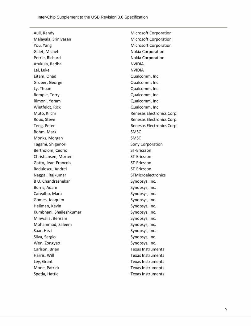
Aull, Randy Microsoft Corporation Malayala, Srinivasan Microsoft Corporation You, Yang Microsoft Corporation Gillet, Michel Nokia Corporation Petrie, Richard Nokia Corporation Atukula, Radha NVIDIA Lai, Luke NVIDIA Eitam, Ohad Qualcomm, Inc Gruber, George Qualcomm, Inc Ly, Thuan Qualcomm, Inc Remple, Terry Qualcomm, Inc Rimoni, Yoram Qualcomm, Inc Wietfeldt, Rick Qualcomm, Inc Muto, Kiichi Renesas Electronics Corp. Roux, Steve Renesas Electronics Corp. Teng, Peter Renesas Electronics Corp. Bohm, Mark SMSC Monks, Morgan SMSC Tagami, Shigenori Sony Corporation Bertholom, Cedric ST-Ericsson Christiansen, Morten ST-Ericsson Gatto, Jean-Francois ST-Ericsson Radulescu, Andrei ST-Ericsson Nagpal, Rajkumar STMicroelectronics B U, Chandrashekar Synopsys, Inc. Burns, Adam Synopsys, Inc. Carvalho, Mara Synopsys, Inc. Gomes, Joaquim Synopsys, Inc. Heilman, Kevin Synopsys, Inc. Kumbhani, Shaileshkumar Synopsys, Inc. Minwalla, Behram Synopsys, Inc. Mohammad, Saleem Synopsys, Inc. Saar, Hezi Synopsys, Inc. Silva, Sergio Synopsys, Inc. Wen, Zongyao Synopsys, Inc. Carlson, Brian Texas Instruments Harris, Will Texas Instruments Ley, Grant Texas Instruments Mone, Patrick Texas Instruments Spetla, Hattie Texas Instruments
Inter-Chip Supplement to the USB Revision 3.0 Specification
vi
Table of Contents
1 Introduction .............................................................................................................................................. 10 1.1 SSIC Significant Features ................................................................................................................ 11 1.2 SSIC and Standard SuperSpeed Comparison ................................................................................. 11 1.3 Related Documents .......................................................................................................................... 12 1.4 Terminology ...................................................................................................................................... 12 1.5 Acronyms and Terms ....................................................................................................................... 12
2 Adaptation of M-PHY for the Physical Layer ........................................................................................ 14 2.1 M-PHY for SSIC Overview ............................................................................................................... 14 2.2 M-PHY MODULE Capabilities .......................................................................................................... 14 2.3 M-PHY Configuration Attributes ....................................................................................................... 21 2.4 M-PHY State Machine ...................................................................................................................... 22 2.5 LS-MODE Support ............................................................................................................................ 22
3 Link Layer ................................................................................................................................................. 31 3.1 Bit and Byte Ordering ....................................................................................................................... 31 3.2 Logical Idle and FLR non-insertion ................................................................................................... 32 3.3 Line Coding ...................................................................................................................................... 33 3.4 Clock Compensation ........................................................................................................................ 34 3.5 Data Scrambling ............................................................................................................................... 36 3.6 PowerOn Reset and Inband Reset ................................................................................................... 37 3.7 Link Layer Timing Requirements ...................................................................................................... 38 3.8 SSIC Link Training and Status State Machine (LTSSM) .................................................................. 39
4 Protocol Layer.......................................................................................................................................... 51 4.1 Port Capability Link Management Packet (LMP) ............................................................................. 51 4.2 Timing Parameters ........................................................................................................................... 51
5 Device Framework ................................................................................................................................... 53 5.1 Dynamic Attachment and Removal .................................................................................................. 53
6 MPHY.TEST .............................................................................................................................................. 55 6.1 Overview ........................................................................................................................................... 55 6.2 Entering MPHY.TEST ....................................................................................................................... 56 6.3 Loopback Testing ............................................................................................................................. 57 6.4 Receive Burst Testing ...................................................................................................................... 58 6.5 Tx Compliance Mode ........................................................................................................................ 58 6.6 Analog Loopback Mode .................................................................................................................... 58 6.7 MPHY.TEST Block Registers ........................................................................................................... 59
7 Timing Diagrams Appendix (Informative) ............................................................................................. 63 7.1 SS.DISABLED TO RX.DETECT ...................................................................................................... 63 7.2 RX.DETECT TO POLLING .............................................................................................................. 64 7.3 POLLING TO U0 .............................................................................................................................. 65 7.4 U0 TO U1 ......................................................................................................................................... 66 7.5 U1 TO U0 ......................................................................................................................................... 67 7.6 U0 TO U2/U3 .................................................................................................................................... 68
Inter-Chip Supplement to the USB Revision 3.0 Specification
vii
7.7 U2/U3 TO U0 .................................................................................................................................... 69 7.8 USP Disconnect ............................................................................................................................... 70 7.9 DSP Disconnect ............................................................................................................................... 71
Inter-Chip Supplement to the USB Revision 3.0 Specification
viii
Figures Figure 1-1 SSIC Layers with modifications from [USB3.0] highlighted ............................................................ 10 Figure 1-2 Example of an implementation with a PHY Adapter Layer to a Standard SS MAC ...................... 11 Figure 2-1 RRAP Packet Types ....................................................................................................................... 23 Figure 3-1 Bit Ordering ..................................................................................................................................... 31 Figure 3-2 Byte Ordering .................................................................................................................................. 31 Figure 3-3 Byte Ordering in a 2 LANE Configuration ....................................................................................... 32 Figure 3-4 Byte Ordering in a 4 LANE Configuration ....................................................................................... 32 Figure 3-5 Two examples of Logical Idle insertion in a 4x LANE configuration ............................................... 33 Figure 3-6 Example of SKP Insertion in a 4x LANE Configuration .................................................................. 35 Figure 3-7 SSIC LTSSM state diagram ........................................................................................................... 40 Figure 3-8 SS.Disabled state ........................................................................................................................... 41 Figure 3-9 Rx.Detect Sub-state Machine ......................................................................................................... 42 Figure 3-10 Polling Sub-state Machine ............................................................................................................ 44 Figure 3-11 U0 Sub-state Machine .................................................................................................................. 47 Figure 6-1 MPHY.TEST Overview .................................................................................................................. 55 Figure 6-2 Example of an MPHY.TEST Block ................................................................................................ 56 Figure 6-3 Receive BURST Test Sequence ................................................................................................... 56
Inter-Chip Supplement to the USB Revision 3.0 Specification
ix
Tables
Table 2-1 Multi-LANE Parameters ................................................................................................................... 15 Table 2-2 M-TX Capability Attributes ............................................................................................................... 16 Table 2-3 M-RX Capability Attributes ............................................................................................................... 18 Table 2-4 TX Configuration Attributes .............................................................................................................. 21 Table 2-5 RRAP Address Map ......................................................................................................................... 24 Table 2-6 RRAP Timing Parameters ............................................................................................................... 30 Table 3-1 Mapping of SS Control Symbols ...................................................................................................... 33 Table 3-2 Link Layer Timing Parameter ........................................................................................................... 38 Table 4-1 Protocol Timing Parameters ............................................................................................................ 51 Table 5-1 Disconnect Timing Parameters ........................................................................................................ 54 Table 6-1 MPHY.TEST Block Registers ......................................................................................................... 59
Inter-Chip Supplement to the USB Revision 3.0 Specification
10
1 Introduction 1
USB is the ubiquitous peripheral-interconnect of choice for a large number of computing and consumer 2 applications. Many systems provide a comprehensive set of software drivers to support commonly 3 available USB peripherals. In addition there is an existing USB ecosystem that includes USB silicon 4 suppliers, design IP houses and verification and testing vendors that lowers the cost for product 5 manufacturers of USB hosts and peripherals. 6
These advantages have made USB attractive as a chip-to-chip interconnect within a product (without 7 use of cables or connectors). This usage has been validated by the adoption of the High Speed Inter-8 Chip Supplement [HSIC] in mobile platforms. HSIC leveraged the benefits of High Speed USB while 9 optimizing the link for power, cost and complexity. However the 480 Mbps bandwidth limitation of HSIC 10 poses a limitation for the next generation of applications that require higher bandwidth. 11
The USB 3.0 specification adds support for transfer speeds of 5 Gbps to address the need for higher 12 bandwidth. However the USB3.0 specification as-is does not meet the requirements of embedded inter-13 chip interfaces with respect to power and EMI robustness. To address this need, this supplement 14 describes Super Speed Inter-Chip (SSIC) as an optimized inter-chip version of USB3.0. 15
16
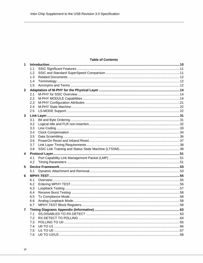
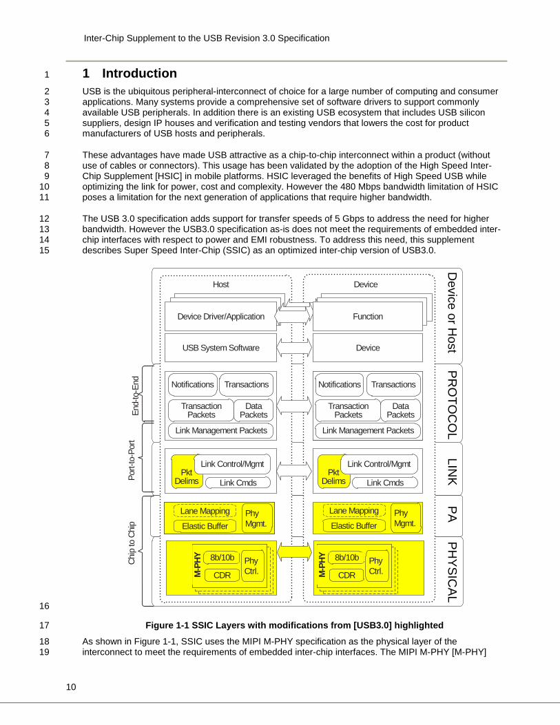
Figure 1-1 SSIC Layers with modifications from [USB3.0] highlighted 17
As shown in Figure 1-1, SSIC uses the MIPI M-PHY specification as the physical layer of the 18 interconnect to meet the requirements of embedded inter-chip interfaces. The MIPI M-PHY [M-PHY] 19
Host
Link Control/Mgmt
Link CmdsPkt
Delims Link CmdsPkt
Delims
Device Driver/Application
USB System Software Device
Notifications Transactions
TransactionPackets
DataPackets
Link Management Packets
Notifications Transactions
TransactionPackets
DataPackets
Link Management Packets
Chip
to C
hip
Port-
to-P
ort
End-
to-E
nd
Device or H
ostP
HY
SIC
AL
PR
OTO
CO
LLIN
K
Link Control/Mgmt
Device
Function
M-P
HY Phy Ctrl.CDR
8b/10b
M-P
HY Phy Ctrl.CDR
8b/10b
Lane Mapping
Elastic BufferPhy Mgmt.
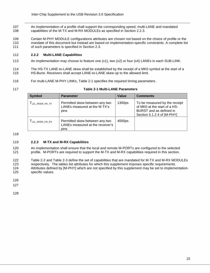
PALane Mapping
Elastic BufferPhy Mgmt.
Inter-Chip Supplement to the USB Revision 3.0 Specification
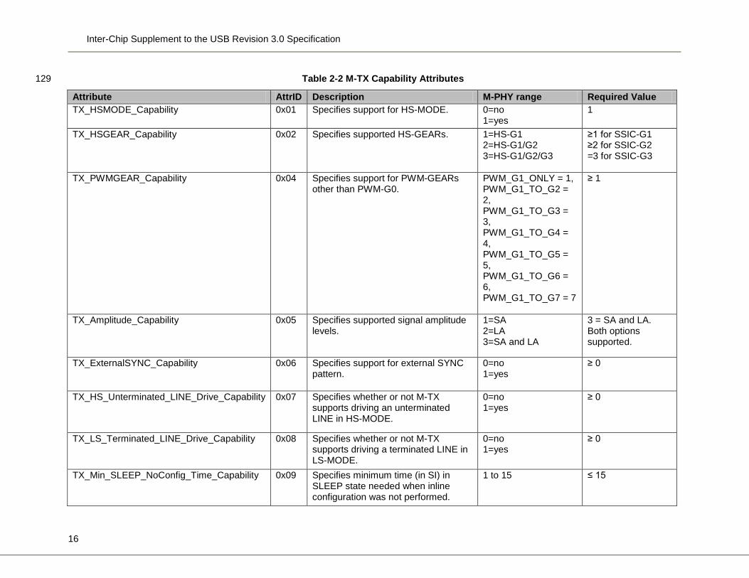
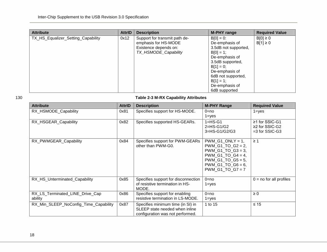
11
specification describes a serial physical layer technology with high bandwidth capabilities, which is 20 specifically developed for mobile applications to obtain low pin count combined with very good power 21 efficiency. 22
1.1 SSIC Significant Features 23
The following summarizes the key features of SSIC: 24
• Support for the SuperSpeed protocol only as defined in [USB 3.0] 25 • Optimized for power, area, cost and EMI robustness for embedded inter-chip interfaces 26 • Compliant with the Type-I M-PORTs from the MIPI M-PHY specification [M-PHY] 27 • Support for x1, x2 and x4 LANE configurations. 28
This supplement only focuses on peripherals that are directly attached to hosts. Support for hubs is not 29 defined and may be achieved in an implementation-specific manner. 30
1.2 SSIC and Standard SuperSpeed Comparison 31
SSIC has been designed to replace a standard SuperSpeed Controller and PHY with an implementation 32 that maps the SuperSpeed controller on the MIPI M-PHY. This supplement does not specify details 33 of any particular implementation and it is intended that SSIC be implementable in multiple ways, 34 depending on what is appropriate for a particular product. 35
36
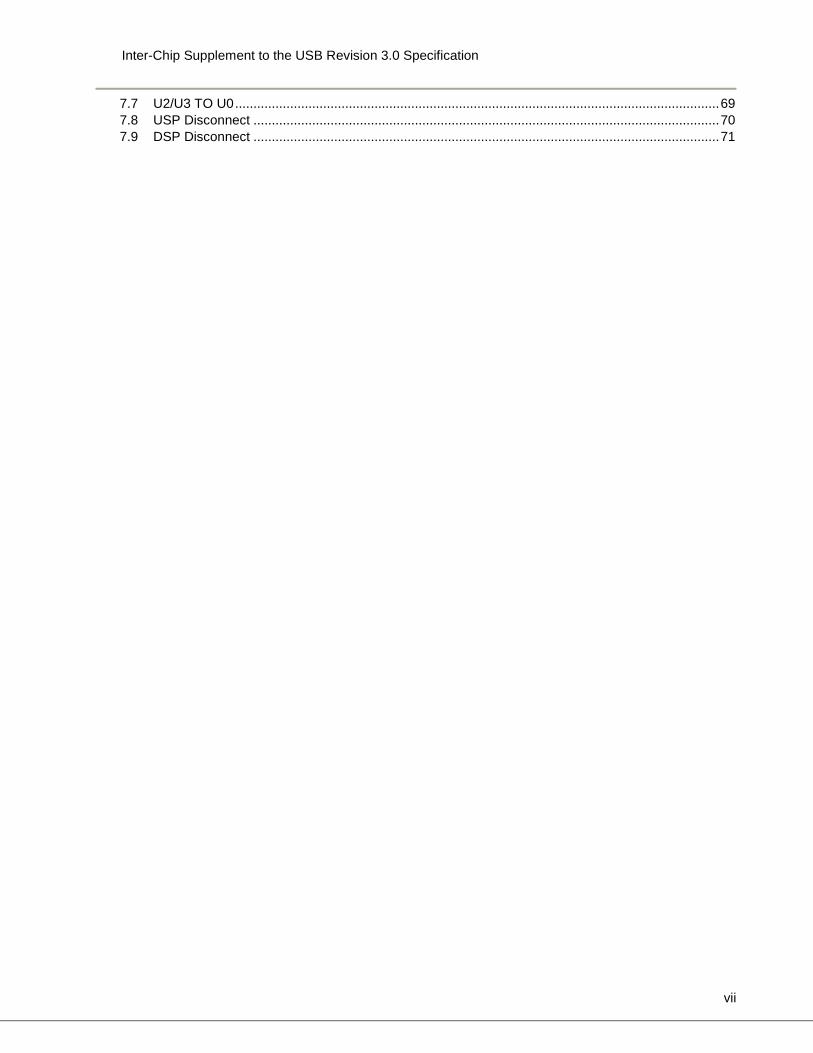
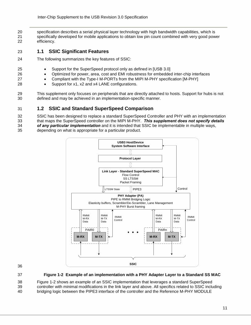
Figure 1-2 Example of an implementation with a PHY Adapter Layer to a Standard SS MAC 37
Figure 1-2 shows an example of an SSIC implementation that leverages a standard SuperSpeed 38 controller with minimal modifications in the link layer and above. All specifics related to SSIC including 39 bridging logic between the PIPE3 interface of the controller and the Reference M-PHY MODULE 40
Link Layer - Standard SuperSpeed MACFlow ControlSS LTSSM
Packet Framing
PHY Adapter (PA)PIPE to RMMI Bridging Logic
Elasticity buffers, Scrambler/De-Scrambler, Lane ManagementM-PHY Burst framing
M-RX M-TX
PAIR0
RMMIM-RXData
RMMIM-TXData
M-RX M-TX
PAIRn
PIPE3LTSSM State
RMMIM-RXData
RMMIM-TXData
RMMIControl
SSIC
Control
RMMIControl
Protocol Layer
USB3 Host/Device System Software Interface
Inter-Chip Supplement to the USB Revision 3.0 Specification
12
Interface (RMMI) of the M-PHY are contained in the PHY Adapter (PA). In such an implementation, it is 41 necessary for the PHY Adapter to implement whatever mechanisms are needed to allow the controller to 42 operate as if it were connected to a SuperSpeed link, for example by tracking the Link Training Status 43 State Machine (LTSSM) and providing the expected responses on the link. Other alternatives to this 44 example may also be designed that are compliant to this supplement. 45
46
1.3 Related Documents 47
This is not a stand-alone document. It is a supplement to [USB 3.0]. Any aspects of USB which are not 48 specifically changed by this supplement are governed by [USB 3.0]. 49
The following referenced documents can be found on the USB-IF website www.usb.org: 50
[USB 3.0] Universal Serial Bus Revision 3.0 Specification including ECNs
[HSIC] High Speed Inter-Chip USB Electrical Specification including ECNs
51
The following referenced documents are published by the MIPI Alliance: 52
[M-PHY] MIPI® Alliance Specification for M-PHYSM Version 3.0
[CTS] MIPI M-PHY Conformance Test Suite
53 1.4 Terminology 54
“Shall” is normative and used to indicate mandatory requirements which are to be followed strictly in 55 order to conform to this standard. 56
“Should” is normative and used to indicate a recommended option or possibility. 57
“May” is normative and used to indicate permitted behavior. 58
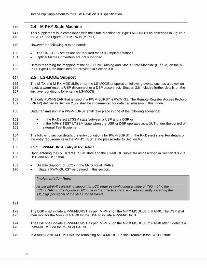
“Can” is informative and used to indicate behavior which is possible or may be seen 59
The use of “must” and “will” is deprecated for requirements and shall only be used for statements of fact. 60
61 1.5 Acronyms and Terms 62
This section lists and defines terms and abbreviations used throughout this specification. 63
Acronyms and Terms defined in [USB 3.0] and [M-PHY] are not reproduced here. Except where explicitly 64 noted, when there is a terminology conflict between the [USB 3.0] and [M-PHY] specifications, the [USB 65 3.0] definition is used in this document. 66
Acronym/Term Description
DSP DownStream Port (DSP) refers to the port of a host to which a peripheral is connected.
Inter-Chip Supplement to the USB Revision 3.0 Specification
13
Link Refers to the Link Layer as defined in [USB 3.0]. To be distinguished from “M-PHY LINK”.
M-PHY LINK Refers to LINK as defined in [M-PHY] .
PA PHY Adapter (PA). Term that refers to logic that interfaces the link layer with the M-PHY.
PAIR A PAIR consists of a LANE in the downstream SUB-LINK and a counterpart LANE in the upstream SUB-LINK.
RRAP Remote Register Access Protocol (RRAP) is used while in the PWM-BURST LS-MODE of operation.
SSIC SuperSpeed Inter-Chip.
USP UpStream Port (USP) refers to the port that a peripheral uses to connect to a host.
67
Inter-Chip Supplement to the USB Revision 3.0 Specification
14
2 Adaptation of M-PHY for the Physical Layer 68
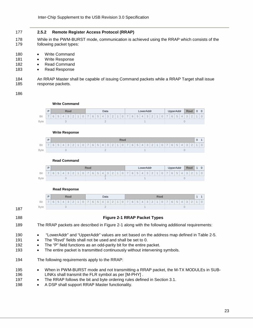
This document references the MIPI M-PHY [M-PHY] specification for the definition of the physical layer. 69 This section includes an overview of the relevant M-PHY features, defines required M-PHY capabilities 70 and describes functionality while in the [M-PHY] LS-MODE of operation. 71
2.1 M-PHY for SSIC Overview 72
The following summarizes relevant M-PHY features: 73
• Requirement to implement Type-I M-PHY 74 • Support for PWM-G1 and HS-G1/G2/G3 BURST mode operation 75 • SSIC profile definitions to aid in inter-operability of M-PHYs in SSIC implementations 76 • M-PHY SAVE states mapped appropriately to SuperSpeed link states 77 • Compliant to M-PHY Symbol coding (8b10b) engine for spectral conditioning and clock recovery 78 • Ability to operate with shared and non-shared reference clocks. 79
2.1.1 M-PHY Architecture and the Definition of PAIRs 80
The architecture of the M-PHY is defined in terms of LANEs, SUB-LINKs and LINKs. The M-PHY LINK 81 shall comply with the following: 82
• The two SUB-LINKs of an SSIC implementation shall support the same number of LANEs. 83 • All LANEs in the M-PHY LINK shall enter and exit HIBERN8 simultaneously. 84
In addition this supplement defines the concept of a PAIR. 85
A LANE in the downstream SUB-LINK and a counterpart LANE in the upstream SUB-LINK are together 86 referred to as a PAIR. A multi-LANE implementation consists of multiple PAIRs and shall have a specific 87 PAIR be statically pre-determined as PAIR0. A single-LANE implementation shall consist of only one 88 PAIR which shall be PAIR0. 89
2.2 M-PHY MODULE Capabilities 90
The M-PHY specification defines capability, configuration and status attributes for an M-TX and for an M-91 RX MODULE. Capability attributes describe the capability of M-PHY MODULEs and may vary 92 depending on the implementation. 93
To aid in the inter-operability of devices, this document defines profiles within which specific M-PHY 94 Capabilities are mandated. 95
2.2.1 Profile Definitions 96
Profiles are indicated by jointly specifying the speed, the multi-LANE capabilities and the rate series such 97 as: 98
SSIC-Ggr-Ll where 99
• g = 1, 2 or 3 and indicates the specific HS-GEAR that the M-PHY LINK operates in 100 • r = A or B and indicates the Rate Series that the M-PHY LINK operates in 101 • l = 1, 2 or 4 and indicates the number of LANEs active in each SUB-LINK (See Section 2.2.2) 102
All lanes in an implementation shall only operate at the HS-GEAR that corresponds to the profile that is 103 supported. An implementation is permitted to support one or more profiles, however the combination of 104 different profiles supported by a specific implementation are out of scope of this specification. For 105 example: an SSIC-G2A-L1 may or may not choose to support SSIC-G1B-L1. 106
Inter-Chip Supplement to the USB Revision 3.0 Specification
15
An implementation of a profile shall support the corresponding speed, multi-LANE and mandated 107 capabilities of the M-TX and M-RX MODULEs as specified in Section 2.2.3. 108
Certain M-PHY MODULE configurations attributes are chosen not based on the choice of profile or the 109 mandate of this document but instead are based on implementation-specific constraints. A complete list 110 of such parameters is specified in Section 2.3. 111
2.2.2 Multi-LANE Capabilities 112
An implementation may choose to feature one (x1), two (x2) or four (x4) LANEs in each SUB-LINK. 113
The HS-TX LANE-to-LANE skew shall be established by the receipt of a MK0 symbol at the start of a 114 HS-Burst. Receivers shall accept LANE-to-LANE skew up to the allowed limit. 115
For multi-LANE M-PHY LINKs, Table 2-1 specifies the required timing parameters. 116
Table 2-1 Multi-LANE Parameters 117
Symbol Parameter Value Comments
TL2L_SKEW_HS_TX Permitted skew between any two LANEs measured at the M-TX’s pins
1300ps To be measured by the receipt of MK0 at the start of a HS-BURST and as defined in Section 5.1.2.4 of [M-PHY]
TL2L_SKEW_HS_RX Permitted skew between any two LANEs measured at the receiver’s pins
4000ps
118
2.2.3 M-TX and M-RX Capabilities 119
An implementation shall ensure that the local and remote M-PORTs are configured to the selected 120 profile. M-PORTs are required to support the M-TX and M-RX capabilities required in this section. 121
Table 2-2 and Table 2-3 define the set of capabilities that are mandated for M-TX and M-RX MODULEs 122 respectively. The tables list attributes for which this supplement imposes specific requirements. 123 Attributes defined by [M-PHY] which are not specified by this supplement may be set to implementation-124 specific values. 125
126 127
128
Inter-Chip Supplement to the USB Revision 3.0 Specification
16
Table 2-2 M-TX Capability Attributes 129
Attribute AttrID Description M-PHY range Required Value TX_HSMODE_Capability 0x01 Specifies support for HS-MODE. 0=no
1=yes 1
TX_HSGEAR_Capability 0x02 Specifies supported HS-GEARs. 1=HS-G1 2=HS-G1/G2 3=HS-G1/G2/G3
≥1 for SSIC-G1 ≥2 for SSIC-G2 =3 for SSIC-G3
TX_PWMGEAR_Capability 0x04 Specifies support for PWM-GEARs other than PWM-G0.
PWM_G1_ONLY = 1, PWM_G1_TO_G2 = 2, PWM_G1_TO_G3 = 3, PWM_G1_TO_G4 = 4, PWM_G1_TO_G5 = 5, PWM_G1_TO_G6 = 6, PWM_G1_TO_G7 = 7
≥ 1
TX_Amplitude_Capability 0x05 Specifies supported signal amplitude levels.
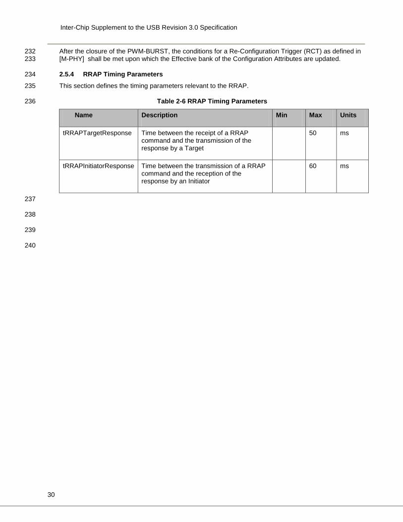
1=SA 2=LA 3=SA and LA
3 = SA and LA. Both options supported.
TX_ExternalSYNC_Capability 0x06 Specifies support for external SYNC pattern.
0=no 1=yes
≥ 0
TX_HS_Unterminated_LINE_Drive_Capability 0x07 Specifies whether or not M-TX supports driving an unterminated LINE in HS-MODE.
0=no 1=yes
≥ 0
TX_LS_Terminated_LINE_Drive_Capability 0x08 Specifies whether or not M-TX supports driving a terminated LINE in LS-MODE.
0=no 1=yes
≥ 0
TX_Min_SLEEP_NoConfig_Time_Capability 0x09 Specifies minimum time (in SI) in SLEEP state needed when inline configuration was not performed.
1 to 15 ≤ 15
Inter-Chip Supplement to the USB Revision 3.0 Specification
17
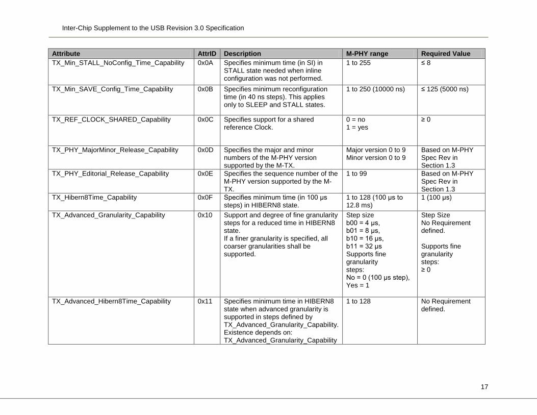
Attribute AttrID Description M-PHY range Required Value TX_Min_STALL_NoConfig_Time_Capability 0x0A Specifies minimum time (in SI) in
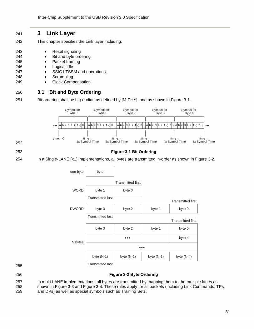
STALL state needed when inline configuration was not performed.
1 to 255 ≤ 8
TX_Min_SAVE_Config_Time_Capability 0x0B Specifies minimum reconfiguration time (in 40 ns steps). This applies only to SLEEP and STALL states.
1 to 250 (10000 ns) ≤ 125 (5000 ns)
TX_REF_CLOCK_SHARED_Capability 0x0C Specifies support for a shared reference Clock.
0 = no 1 = yes
≥ 0
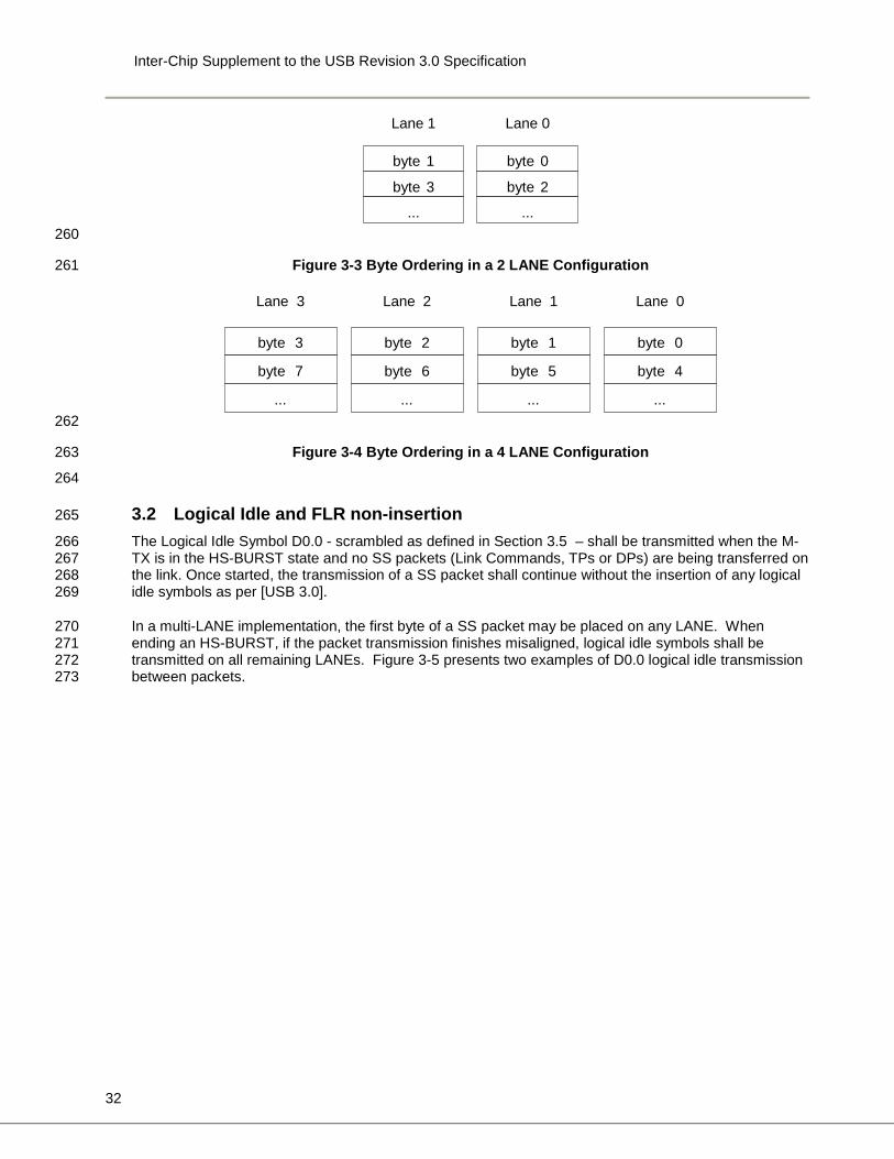
TX_PHY_MajorMinor_Release_Capability 0x0D Specifies the major and minor numbers of the M-PHY version supported by the M-TX.
Major version 0 to 9 Minor version 0 to 9
Based on M-PHY Spec Rev in Section 1.3
TX_PHY_Editorial_Release_Capability 0x0E Specifies the sequence number of the M-PHY version supported by the M-TX.
1 to 99 Based on M-PHY Spec Rev in Section 1.3
TX_Hibern8Time_Capability 0x0F Specifies minimum time (in 100 μs steps) in HIBERN8 state.
1 to 128 (100 μs to 12.8 ms)
1 (100 μs)
TX_Advanced_Granularity_Capability 0x10 Support and degree of fine granularity steps for a reduced time in HIBERN8 state. If a finer granularity is specified, all coarser granularities shall be supported.
Step size b00 = 4 μs, b01 = 8 μs, b10 = 16 μs, b11 = 32 μs Supports fine granularity steps: No = 0 (100 μs step), Yes = 1
Step Size No Requirement defined. Supports fine granularity steps: ≥ 0
TX_Advanced_Hibern8Time_Capability 0x11 Specifies minimum time in HIBERN8 state when advanced granularity is supported in steps defined by TX_Advanced_Granularity_Capability. Existence depends on: TX_Advanced_Granularity_Capability
1 to 128 No Requirement defined.
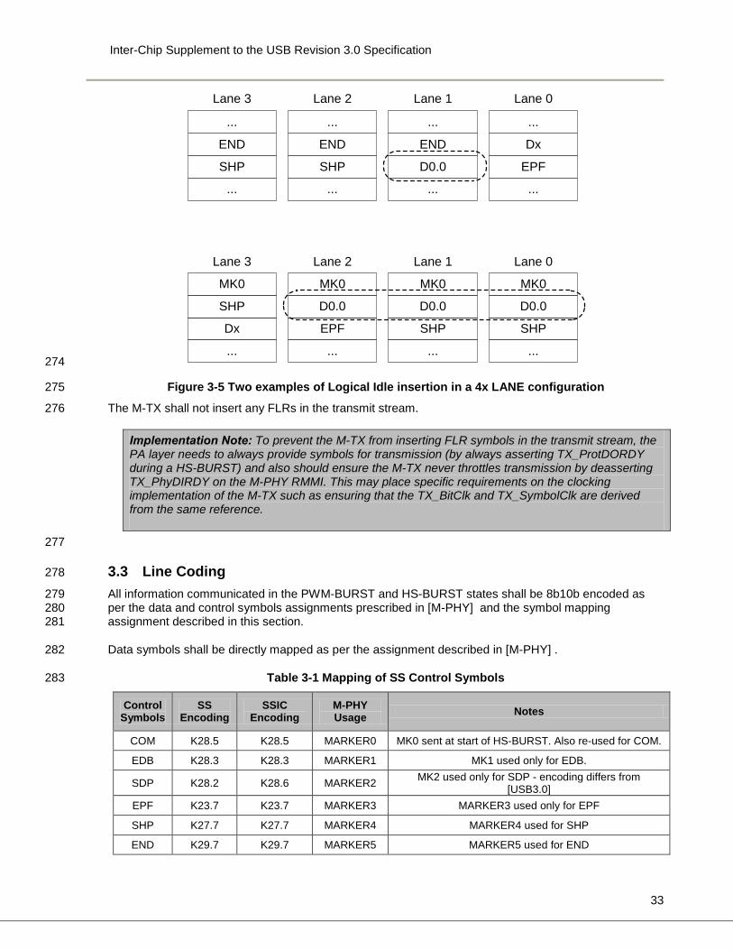
Inter-Chip Supplement to the USB Revision 3.0 Specification
18
Attribute AttrID Description M-PHY range Required Value TX_HS_Equalizer_Setting_Capability 0x12 Support for transmit path de-
emphasis for HS-MODE Existence depends on: TX_HSMODE_Capability
B[0] = 0: De-emphasis of 3.5dB not supported, B[0] = 1; De-emphasis of 3.5dB supported, B[1] = 0; De-emphasis of 6dB not supported, B[1] = 1; De-emphasis of 6dB supported
B[0] ≥ 0 B[1] ≥ 0
Table 2-3 M-RX Capability Attributes 130
Attribute AttrID Description M-PHY Range Required Value RX_HSMODE_Capability 0x81 Specifies support for HS-MODE. 0=no
1=yes 1=yes
RX_HSGEAR_Capability 0x82 Specifies supported HS-GEARs. 1=HS-G1 2=HS-G1/G2 3=HS-G1/G2/G3
≥1 for SSIC-G1 ≥2 for SSIC-G2 =3 for SSIC-G3
RX_PWMGEAR_Capability 0x84 Specifies support for PWM-GEARs other than PWM-G0.
PWM_G1_ONLY = 1, PWM_G1_TO_G2 = 2, PWM_G1_TO_G3 = 3, PWM_G1_TO_G4 = 4, PWM_G1_TO_G5 = 5, PWM_G1_TO_G6 = 6, PWM_G1_TO_G7 = 7
≥ 1
RX_HS_Unterminated_Capability 0x85 Specifies support for disconnection of resistive termination in HS-MODE.
0=no 1=yes
0 = no for all profiles
RX_LS_Terminated_LINE_Drive_Cap ability
0x86 Specifies support for enabling resistive termination in LS-MODE.
0=no 1=yes
≥ 0
RX_Min_SLEEP_NoConfig_Time_Capability 0x87 Specifies minimum time (in SI) in SLEEP state needed when inline configuration was not performed.
1 to 15 ≤ 15
Inter-Chip Supplement to the USB Revision 3.0 Specification
19
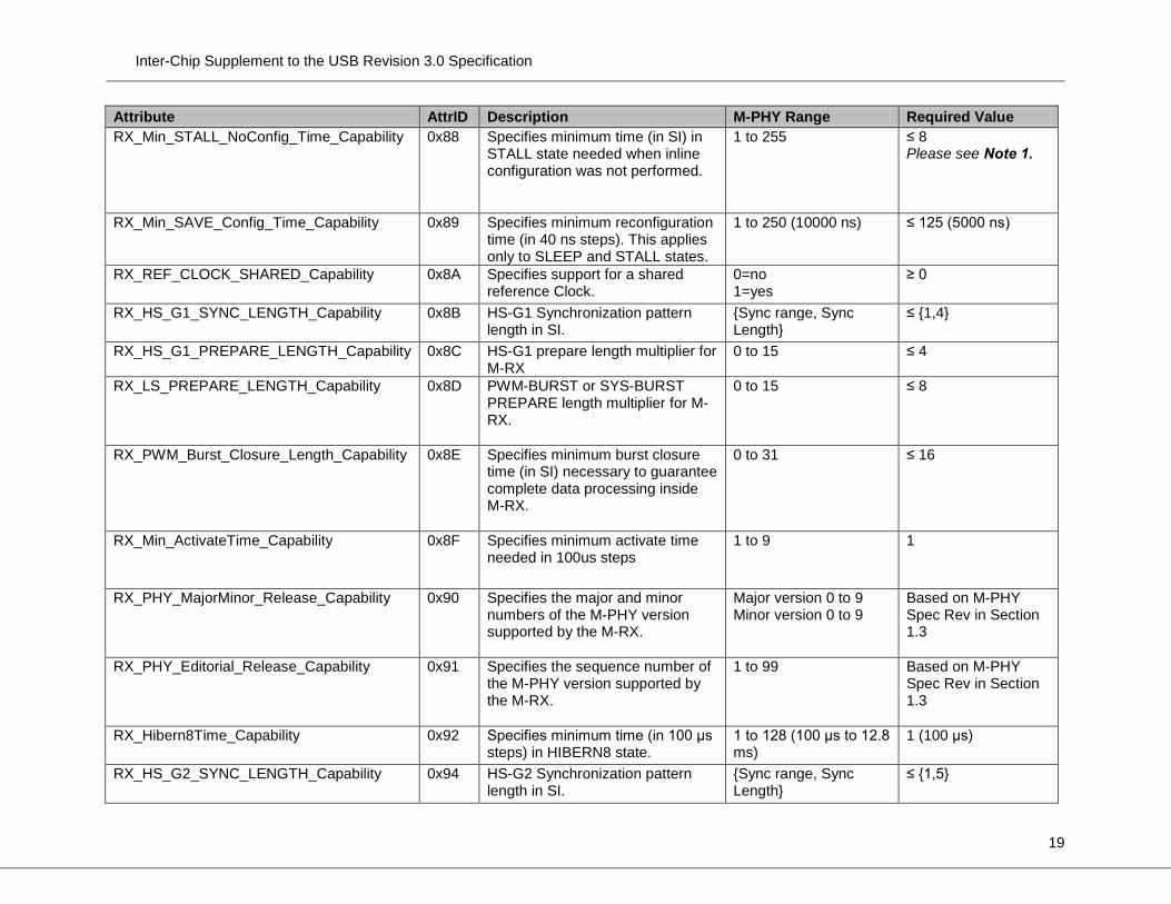
Attribute AttrID Description M-PHY Range Required Value RX_Min_STALL_NoConfig_Time_Capability 0x88 Specifies minimum time (in SI) in
STALL state needed when inline configuration was not performed.
1 to 255 ≤ 8 Please see Note 1.
RX_Min_SAVE_Config_Time_Capability 0x89 Specifies minimum reconfiguration time (in 40 ns steps). This applies only to SLEEP and STALL states.
1 to 250 (10000 ns) ≤ 125 (5000 ns)
RX_REF_CLOCK_SHARED_Capability 0x8A Specifies support for a shared reference Clock.
0=no 1=yes
≥ 0
RX_HS_G1_SYNC_LENGTH_Capability 0x8B HS-G1 Synchronization pattern length in SI.
{Sync range, Sync Length}
≤ {1,4}
RX_HS_G1_PREPARE_LENGTH_Capability 0x8C HS-G1 prepare length multiplier for M-RX
0 to 15 ≤ 4
RX_LS_PREPARE_LENGTH_Capability 0x8D PWM-BURST or SYS-BURST PREPARE length multiplier for M-RX.
0 to 15 ≤ 8
RX_PWM_Burst_Closure_Length_Capability 0x8E Specifies minimum burst closure time (in SI) necessary to guarantee complete data processing inside M-RX.
0 to 31 ≤ 16
RX_Min_ActivateTime_Capability 0x8F Specifies minimum activate time needed in 100us steps
1 to 9 1
RX_PHY_MajorMinor_Release_Capability 0x90 Specifies the major and minor numbers of the M-PHY version supported by the M-RX.
Major version 0 to 9 Minor version 0 to 9
Based on M-PHY Spec Rev in Section 1.3
RX_PHY_Editorial_Release_Capability 0x91 Specifies the sequence number of the M-PHY version supported by the M-RX.
1 to 99 Based on M-PHY Spec Rev in Section 1.3
RX_Hibern8Time_Capability 0x92 Specifies minimum time (in 100 μs steps) in HIBERN8 state.
1 to 128 (100 μs to 12.8 ms)
1 (100 μs)
RX_HS_G2_SYNC_LENGTH_Capability 0x94 HS-G2 Synchronization pattern length in SI.
{Sync range, Sync Length}
≤ {1,5}
Inter-Chip Supplement to the USB Revision 3.0 Specification
20
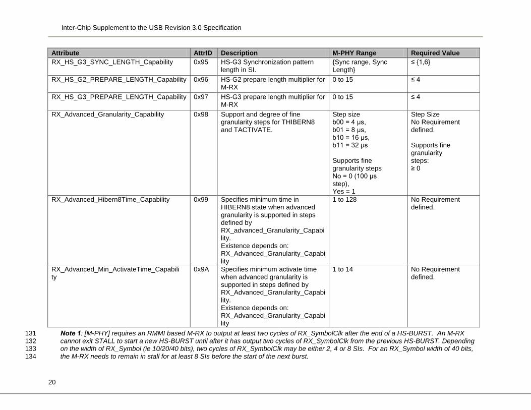
Attribute AttrID Description M-PHY Range Required Value RX_HS_G3_SYNC_LENGTH_Capability 0x95 HS-G3 Synchronization pattern
length in SI. {Sync range, Sync Length}
≤ {1,6}
RX_HS_G2_PREPARE_LENGTH_Capability 0x96 HS-G2 prepare length multiplier for M-RX
0 to 15 ≤ 4
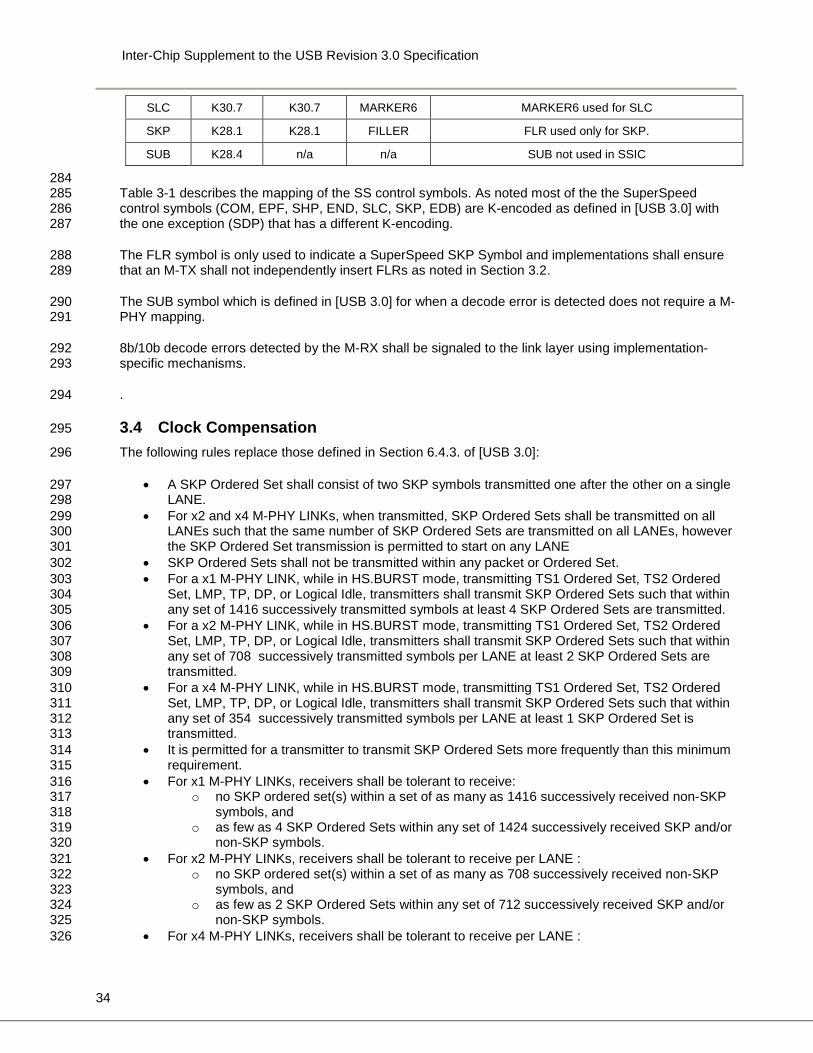
RX_HS_G3_PREPARE_LENGTH_Capability 0x97 HS-G3 prepare length multiplier for M-RX
0 to 15 ≤ 4
RX_Advanced_Granularity_Capability 0x98 Support and degree of fine granularity steps for THIBERN8 and TACTIVATE.
Step size b00 = 4 μs, b01 = 8 μs, b10 = 16 μs, b11 = 32 μs Supports fine granularity steps No = 0 (100 μs step), Yes = 1
Step Size No Requirement defined. Supports fine granularity steps: ≥ 0
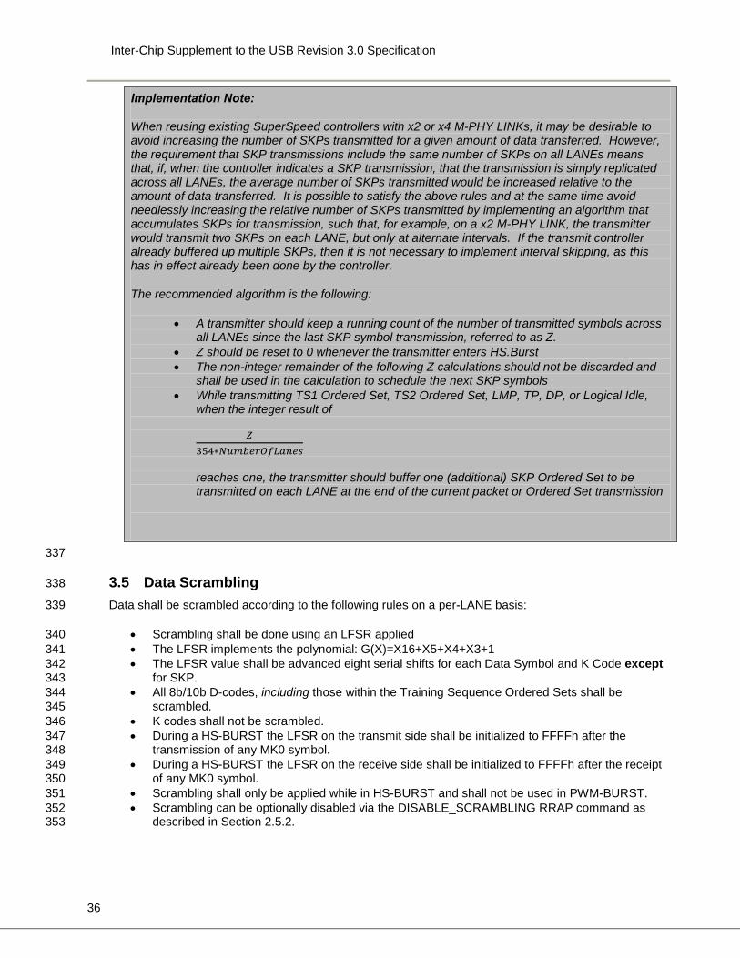
RX_Advanced_Hibern8Time_Capability 0x99 Specifies minimum time in HIBERN8 state when advanced granularity is supported in steps defined by RX_advanced_Granularity_Capability. Existence depends on: RX_Advanced_Granularity_Capability
1 to 128 No Requirement defined.
RX_Advanced_Min_ActivateTime_Capabili ty
0x9A Specifies minimum activate time when advanced granularity is supported in steps defined by RX_Advanced_Granularity_Capability. Existence depends on: RX_Advanced_Granularity_Capability
1 to 14 No Requirement defined.
Note 1: [M-PHY] requires an RMMI based M-RX to output at least two cycles of RX_SymbolClk after the end of a HS-BURST. An M-RX 131 cannot exit STALL to start a new HS-BURST until after it has output two cycles of RX_SymbolClk from the previous HS-BURST. Depending 132 on the width of RX_Symbol (ie 10/20/40 bits), two cycles of RX_SymbolClk may be either 2, 4 or 8 SIs. For an RX_Symbol width of 40 bits, 133 the M-RX needs to remain in stall for at least 8 SIs before the start of the next burst. 134
Inter-Chip Supplement to the USB Revision 3.0 Specification
21
135
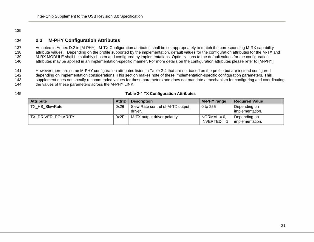
2.3 M-PHY Configuration Attributes 136
As noted in Annex D.2 in [M-PHY] , M-TX Configuration attributes shall be set appropriately to match the corresponding M-RX capability 137 attribute values. Depending on the profile supported by the implementation, default values for the configuration attributes for the M-TX and 138 M-RX MODULE shall be suitably chosen and configured by implementations. Optimizations to the default values for the configuration 139 attributes may be applied in an implementation-specific manner. For more details on the configuration attributes please refer to [M-PHY] 140
However there are some M-PHY configuration attributes listed in Table 2-4 that are not based on the profile but are instead configured 141 depending on implementation considerations. This section makes note of these implementation-specific configuration parameters. This 142 supplement does not specify recommended values for these parameters and does not mandate a mechanism for configuring and coordinating 143 the values of these parameters across the M-PHY LINK. 144
Table 2-4 TX Configuration Attributes 145
Attribute AttrID Description M-PHY range Required Value TX_HS_SlewRate 0x26 Slew Rate control of M-TX output
driver. 0 to 255 Depending on
implementation. TX_DRIVER_POLARITY 0x2F M-TX output driver polarity. NORMAL = 0,
INVERTED = 1 Depending on implementation.
Inter-Chip Supplement to the USB Revision 3.0 Specification
22
2.4 M-PHY State Machine 146
This supplement is in compliance with the State Machine for Type-I MODULEs as described in Figure 7 147 for M-TX and Figure 8 for M-RX in [M-PHY] . 148
However the following is to be noted: 149
• The LINE-CFG states are not required for SSIC implementations. 150 • Optical Media Converters are not supported. 151
Details regarding the mapping of the SSIC Link Training and Status State Machine (LTSSM) on the M-152 PHY Type-I state machines are provided in Section 3.8. 153
2.5 LS-MODE Support 154
The M-TX and M-RX MODULEs enter the LS-MODE of operation following events such as a power-on-155 reset, a warm reset, a USP disconnect or a DSP disconnect. Section 3.8 includes further details on the 156 link layer conditions for entering LS-MODE. 157
The only PWM-GEAR that is used in a PWM-BURST is PWM-G1. The Remote Register Access Protocol 158 (RRAP) defined in Section 2.5.2 shall be implemented for data transmission in this mode. 159
Data transmission in a PWM-BURST shall take place in one of the following scenarios: 160
• In the Rx.Detect LTSSM state between a USP and a DSP or 161 • in the MPHY.TEST LTSSM state when the USP or DSP operates as a DUT under the control of 162
external Test Equipment. 163
The following section details the entry conditions for PWM-BURST in the Rx.Detect state. For details on 164 the entry requirements in the MPHY.TEST state please refer to Section 6.2. 165
2.5.1 PWM-BURST Entry in Rx.Detect 166
Upon entering the Rx.Detect LTSSM state and the LS-MODE sub-state as described in Section 3.8.2, a 167 DSP and an USP shall: 168
• Disable Support for LCCs in the M-TX for all PAIRs. 169 • Initiate a PWM-BURST as defined in this section. 170
Implementation Note:
As per [M-PHY] disabling support for LCC requires configuring a value of “NO = 0” to the LCC_ENABLE Configuration Attribute in the Effective Bank and subsequently asserting the TX_CfgUpdt signal of the M-TX for all PAIRs.
171
The DSP shall initiate a PWM-BURST as per [M-PHY] on the M-TX MODULE of PAIR0. The DSP shall 172 then monitor the M-RX of PAIR0 for the USP to initiate a PWM-BURST. 173
The USP shall initiate a PWM-BURST as per [M-PHY] on the M-TX MODULE of PAIR0 after it detects a 174 PWM-BURST on the M-RX of PAIR0. 175
In a multi-LANE M-PHY LINK the remaining M-TX MODULEs shall remain in the SLEEP state. 176
Inter-Chip Supplement to the USB Revision 3.0 Specification
23
2.5.2 Remote Register Access Protocol (RRAP) 177
While in the PWM-BURST mode, communication is achieved using the RRAP which consists of the 178 following packet types: 179
• Write Command 180 • Write Response 181 • Read Command 182 • Read Response 183
An RRAP Master shall be capable of issuing Command packets while a RRAP Target shall issue 184 response packets. 185
186
187
Figure 2-1 RRAP Packet Types 188
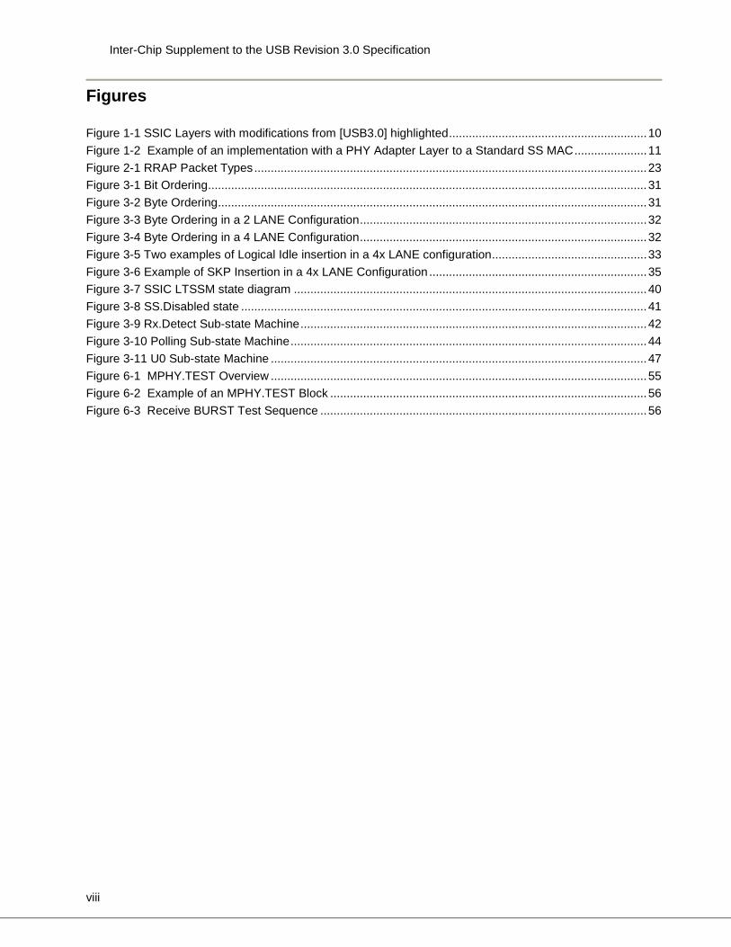
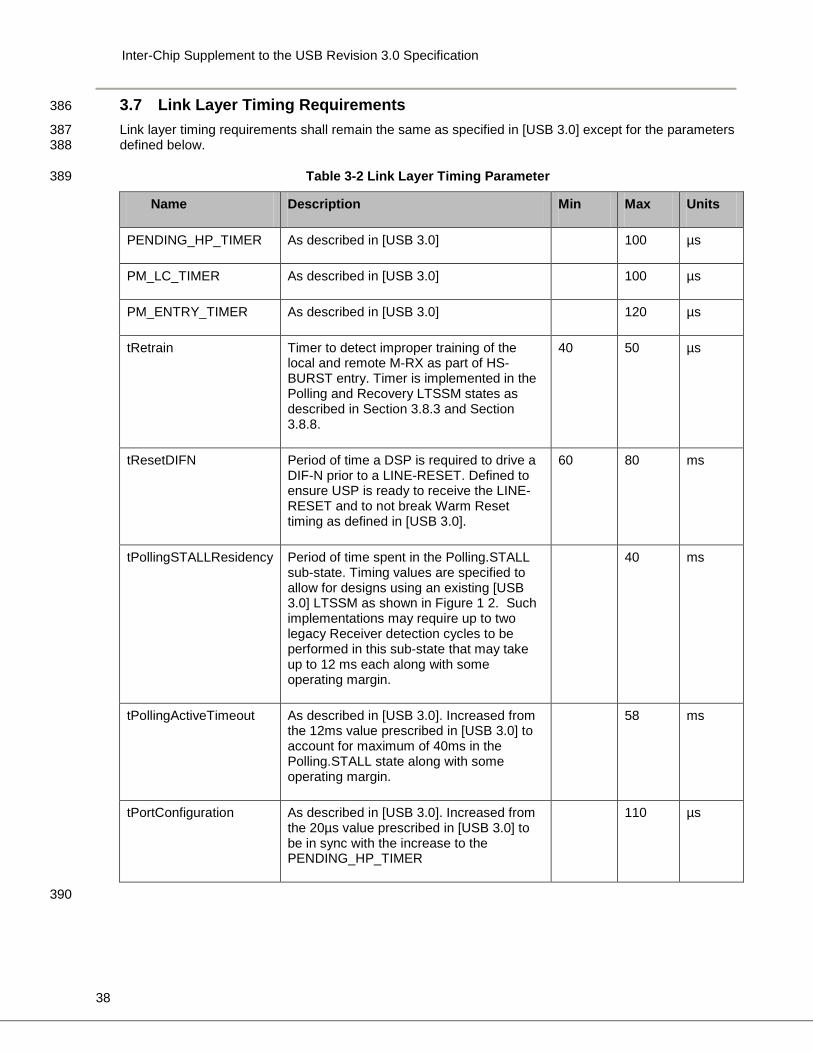
The RRAP packets are described in Figure 2-1 along with the following additional requirements: 189
• “LowerAddr” and “UpperAddr” values are set based on the address map defined in Table 2-5. 190 • The “Rsvd” fields shall not be used and shall be set to 0. 191 • The “P” field functions as an odd-parity bit for the entire packet. 192 • The entire packet is transmitted continuously without intervening symbols. 193
The following requirements apply to the RRAP: 194
• When in PWM-BURST mode and not transmitting a RRAP packet, the M-TX MODULEs in SUB-195 LINKs shall transmit the FLR symbol as per [M-PHY] . 196
• The RRAP follows the bit and byte ordering rules defined in Section 3.1. 197 • A DSP shall support RRAP Master functionality. 198
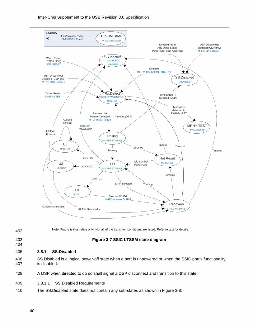
012
01234567Bit 01234567 01234567 1234567 0
Byte 3
UpperAddr 0 0LowerAddrData
Write Command
P Rsvd Rsvd
012
01234567Bit 01234567 01234567 1234567 0
Byte 3
Write Response
0121
01234567Bit 01234567 01234567 1234567 0
Byte 3
Read Command
012
01234567Bit 01234567 01234567 1234567 0
Byte 3
Read Response
0 1P Rsvd
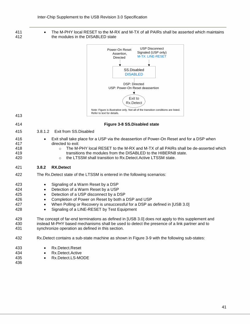
UpperAddr 1 0LowerAddrP Rsvd Rsvd
1 1P RsvdDataRsvd
Inter-Chip Supplement to the USB Revision 3.0 Specification
24
• When in PWM-BURST, a DSP that supports the optional MPHY.TEST state shall support the receipt 199 of a Write Command to enable a transition to that state. All RRAP commands received by a DSP in 200 the MPHY.TEST state shall be processed per RRAP Target functionality. 201
• A USP shall only support RRAP Target functionality. 202 • Test Equipment shall function as a RRAP Master with either the DSP or the USP as the Device 203
Under Test (DUT). 204 • A DSP serving as a RRAP Master shall only send commands and receive responses on PAIR0. 205 • A DSP or an USP serving as a RRAP Target shall support receiving commands over any PAIRx and 206
shall return a response on the same PAIRx. 207 • Test Equipment serving as a RRAP Master may send commands and receive responses on any 208
PAIR. 209 • Upon receiving a Write Command packet, a Target shall transmit the corresponding response 210
packet within tRRAPTargetResponse. This requirement shall apply for any Write Command received 211 including Writes to Reserved Registers and Registers that are identified in Table 2-5 as having no 212 effect. 213
• Upon receiving a Read Command packet, a Target shall transmit the corresponding response 214 packet within tRRAPTargetResponse. 215
• If a Master has issued a Command, then the Master shall not retry the Command or issue another 216 Command until either the Target has provided a Response, or after tRRAPInitiatorResponse has 217 elapsed. 218
• A Target shall map the attributes of all implemented PAIRs to RRAP addresses as defined in Table 219 2-5. 220
• A Target shall not send a response until the RRAP Command is fully received with a valid parity. 221
Implementation Note:
Additional steps to improve the reliability offered by a single parity bit may be taken at the RRAP level using implementation specific means such as redundant write commands or performing reads after writes to ensure the correctness of operations.
222
Table 2-5 RRAP Address Map 223
UpperAddr LowerAddr Register Name Description
0x0 0x00-0xFF As defined in [M-PHY] Capability, configuration and status attributes for PAIR0. Writes to these registers shall only affect the shadow bank until an RCT is executed. The Target shall provide a Write Response only after the corresponding Register Write specified in the RRAP Command is committed to the shadow bank.
0x1 0x00-0xFF As defined in [M-PHY] Capability, configuration and status attributes for PAIR1. Writes to these registers shall only affect the shadow bank until an RCT is executed. The Target shall provide a Write Response only after the corresponding Register Write specified in the RRAP Command is committed to the shadow bank.
Inter-Chip Supplement to the USB Revision 3.0 Specification
25
UpperAddr LowerAddr Register Name Description
0x2 0x00-0xFF As defined in [M-PHY] Capability, configuration and status attributes for PAIR2. Writes to these registers shall only affect the shadow bank until an RCT is executed. The Target shall provide a Write Response only after the corresponding Register Write specified in the RRAP Command is committed to the shadow bank.
0x3 0x00-0xFF As defined in [M-PHY] Capability, configuration and status attributes for PAIR3. Writes to these registers shall only affect the shadow bank until an RCT is executed. The Target shall provide a Write Response only after the corresponding Register Write specified in the RRAP Command is committed to the shadow bank.
0x4 0x00 DSP_DISCONNECT This Register is used by a DSP following a LINE-RESET to signal a DSP Disconnect. This bit is required only for an USP only. A DSP or a USP in the MPHY.TEST state shall ignore writes to this register.
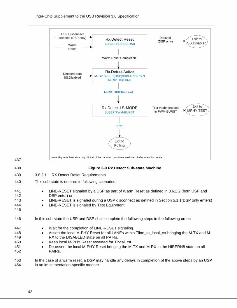
Read/Write Attributes:
• R/W
Reset Default:
• 0x00
Bit [0]:
• Writing 1’b1 signals a DSP disconnect as detailed in Section 5.1.2.
• Writing 1’b0 shall have no effect.
Once the bit is set, it shall only be reset via a LINE-RESET issued either by a DSP (as part of Warm Reset) or by Test Equipment.
Bit [7:1] Reserved.
• Writes shall be ignored and Reads shall return zero values.
0x4 0x01 CONFIGURE_FOR_HS This Register is used to direct the Target to update its shadow bank for HS-BURST with the settings that correspond to the SSIC profile supported. As noted in Section 2.2.1 this profile is statically determined and this supplement provides no means for selecting between different profiles if so supported. The Target shall provide a Write Response only after the corresponding Register Write specified in the RRAP Command is committed to the shadow bank.
Inter-Chip Supplement to the USB Revision 3.0 Specification
26
UpperAddr LowerAddr Register Name Description
A Master may alternatively choose to not use this register in which case it shall rely on a set of implementation-specific RRAP commands to update the shadow bank of the Target for HS-BURST operation.
Read/Write Attributes:
• R/W
Reset Default:
• 0x00
Bit [0]:
• Writing 1’b1 directs the Target to update its shadow bank with the settings that correspond to its SSIC profile.
• Writing 1’b0 shall have no effect.
Once the bit is set, it shall only be reset via a LINE-RESET issued either by a DSP (as part of Warm Reset) or by Test Equipment.
Bit[7:1] Reserved.
• Writes shall be ignored and Reads shall return zero values.
0x4 0x02 BURST_CLOSURE This Register is used to direct the Target to terminate the PWM-BURST.
Read/Write Attributes:
• R/W
Reset Default:
• 0x00
Bit [0]:
• Writing 1’b1 terminates the PWM-BURST and initiates an RCT to exit LS-MODE as defined in Section 2.5.3.
• Writing 1’b0 shall have no effect.
Once the bit is set, it shall only be reset via a LINE-RESET issued either by a DSP (as part of Warm Reset) or by Test Equipment.
Bit[7:1] Reserved.
• Writes shall be ignored and Reads shall return zero values.
0x4 0x03 DISABLE_SCRAMBLING This Register is used by a DSP to indicate to an USP that data transmission in HS-MODE shall
Inter-Chip Supplement to the USB Revision 3.0 Specification
27
UpperAddr LowerAddr Register Name Description
have scrambling disabled.
Read/Write Attributes:
• R/W
Reset Default:
• 0x00
Bit [0]:
• Writing 1’b1 configures the USP to disable HS-MODE scrambling.
• Writing 1’b0 shall have no effect.
Once the bit is set, it shall only be reset via a LINE-RESET issued either by a DSP (as part of Warm Reset) or by Test Equipment.
Bit [7:1] Reserved.
• Writes shall be ignored and Reads shall return zero values.
0x4 0x04 DISABLE_STALL_IN_U0 This Register is used by a DSP to disable STALL entry in U0 in an USP. A DSP or a USP in the MPHY.TEST state shall ignore writes to this register.
Read/Write Attributes:
• R/W
Reset Default:
• 0x00
Bit [0]:
• Writing 1’b1 configures the USP to disable STALL entry while in U0.
• Writing 1’b0 shall have no effect.
Once the bit is set, it shall only be reset via a LINE-RESET issued either by a DSP (as part of Warm Reset) or by Test Equipment.
Bit [7:1] Reserved.
• Writes shall be ignored and Reads shall return zero values.
0x4 0x05 DISABLE_LUP_LDN This optional Register is used by a DSP to disable the use of the LDN and LUP Link Commands defined in [USB 3.0] to allow additional power optimizations in the M-TX.
Read/Write Attributes:
• R/W
Reset Default:
Inter-Chip Supplement to the USB Revision 3.0 Specification
28
UpperAddr LowerAddr Register Name Description
• 0x00
Bit [0]:
• Writing 1’b1 configures the USP to disable LUP/LDN commands. In addition, the USP shall not flag a tU0LTimeout Error or transition to Recovery upon detecting a missing LUP or LDN.
• A DSP that generates a RRAP command to set this bit shall not transmit any LUP and LDN link commands. In addition, the DSP shall not flag a tU0LTimeout Error or transition to Recovery upon detecting a missing LUP or LDN.
• Writing 1’b0 shall have no effect.
Once the bit is set, it shall only be reset via a LINE-RESET issued either by a DSP (as part of Warm Reset) or by Test Equipment.
Bit [7:1] Reserved.
• Writes shall be ignored and Reads shall return zero values.
0x4 0x05-0xFE RESERVED Reserved. Writes shall be ignored and Reads shall return zero values.
0x4 0xFF TEST_MODE This Register is used by Test Equipment to configure a Target in the MPHY.TEST state. The Target shall complete its configuration to the MPHY.TEST state prior to issuing a Write Response to the command.
Read/Write Attributes:
• R/W
Reset Default:
• 0x00
Bit [0]:
• Writing 1’b1 configures the RRAP Target in the MPHY.TEST state.
• Writing 1’b0 shall have no effect.
Once the bit is set, it shall only be reset via a LINE-RESET issued either by a DSP (as part of Warm Reset) or by Test Equipment.
Bit [7:1] Reserved.
• Writes shall be ignored and Reads shall return zero values.
Inter-Chip Supplement to the USB Revision 3.0 Specification
29
UpperAddr LowerAddr Register Name Description
0x5 0x00 PAIR_CAPABILITY This Register is used by a Master to determine the number PAIRs supported by a Target.
Read/Write Attributes:
• RO • Writes to this register shall be ignored.
Reset Default:
• Implementation-specific.
Bit [0]:
• A read of this field shall always return a value of 1’b1
Bit [1]:
• A read of this field shall return a value of 1’b1 if PAIR0 and PAIR1 are supported.
Bit [2]:
• A read of this field shall return a value of 1’b1 if PAIR0, PAIR1, PAIR2 and PAIR3 are supported.
Bit [7:3] Reserved.
• Reads shall return zero values.
0x5 0x01- 0xFF RESERVED Reserved. Writes shall be ignored and Reads shall return zero values.
0x6-0xD 0x00-0xFF RESERVED Reserved. Writes shall be ignored and Reads shall return zero values.
0xE 0x00-0xFF MPHY.TEST Registers Refer to Section 6.
0xF 0x00-0xFF VENDOR-SPECIFIC REGISTERS
Registers in this address space are not defined in this specification and are reserved to implement vendor-specific functionality.
224
2.5.3 PWM-BURST Closure 225
PWM-BURST closure shall be implemented in the following manner: 226
• The Master shall set BURST_CLOSURE[0] register in the Target. 227 • Upon the receipt of a Write Response with a valid parity from the Target, the Master shall end the 228
PWM-BURST on its M-TX. 229 • On detecting the closure of the PWM-BURST on its M-RX, the RRAP Target shall end the PWM-230
BURST on its M-TX. 231
Inter-Chip Supplement to the USB Revision 3.0 Specification
30
After the closure of the PWM-BURST, the conditions for a Re-Configuration Trigger (RCT) as defined in 232 [M-PHY] shall be met upon which the Effective bank of the Configuration Attributes are updated. 233
2.5.4 RRAP Timing Parameters 234
This section defines the timing parameters relevant to the RRAP. 235
Table 2-6 RRAP Timing Parameters 236
Name Description Min Max Units
tRRAPTargetResponse Time between the receipt of a RRAP command and the transmission of the response by a Target
50 ms
tRRAPInitiatorResponse Time between the transmission of a RRAP command and the reception of the response by an Initiator
60 ms
237
238
239
240
Inter-Chip Supplement to the USB Revision 3.0 Specification
31
3 Link Layer 241
This chapter specifies the Link layer including: 242
• Reset signaling 243 • Bit and byte ordering 244 • Packet framing 245 • Logical idle 246 • SSIC LTSSM and operations 247 • Scrambling 248 • Clock Compensation 249
3.1 Bit and Byte Ordering 250
Bit ordering shall be big-endian as defined by [M-PHY] and as shown in Figure 3-1. 251
252
Figure 3-1 Bit Ordering 253
In a Single-LANE (x1) implementations, all bytes are transmitted in-order as shown in Figure 3-2. 254
255
Figure 3-2 Byte Ordering 256
In multi-LANE implementations, all bytes are transmitted by mapping them to the multiple lanes as 257 shown in Figure 3-3 and Figure 3-4. These rules apply for all packets (including Link Commands, TPs 258 and DPs) as well as special symbols such as Training Sets. 259
a b c d e i f g h j a b c d e i f g h j a b c d e i f g h j a b c d e i f g h j a b c d e i f g h j
Symbol for Byte 0
time = 0 time =1x Symbol Time
time =2x Symbol Time
time =3x Symbol Time
time =5x Symbol Time
time =4x Symbol Time
Symbol for Byte 1
Symbol for Byte 2
Symbol for Byte 3
Symbol for Byte 4
byte 3 byte 2 byte 1 byte 0
byte 1 byte 0
Transmitted first
byte
byte 3
DWORD
WORD
one byte
N bytes
byte 2 byte 1 byte 0
Transmitted first
Transmitted first
byte 4
byte (N-1)
Transmitted last
Transmitted last
Transmitted last
byte (N-2) byte (N-3) byte (N-4)
Inter-Chip Supplement to the USB Revision 3.0 Specification
32
260
Figure 3-3 Byte Ordering in a 2 LANE Configuration 261
262
Figure 3-4 Byte Ordering in a 4 LANE Configuration 263
264
3.2 Logical Idle and FLR non-insertion 265
The Logical Idle Symbol D0.0 - scrambled as defined in Section 3.5 – shall be transmitted when the M-266 TX is in the HS-BURST state and no SS packets (Link Commands, TPs or DPs) are being transferred on 267 the link. Once started, the transmission of a SS packet shall continue without the insertion of any logical 268 idle symbols as per [USB 3.0]. 269
In a multi-LANE implementation, the first byte of a SS packet may be placed on any LANE. When 270 ending an HS-BURST, if the packet transmission finishes misaligned, logical idle symbols shall be 271 transmitted on all remaining LANEs. Figure 3-5 presents two examples of D0.0 logical idle transmission 272 between packets. 273
byte 0 byte 1
byte 4 byte 5
... ...
Lane 0 Lane 1
byte 2 byte 3
byte 6 byte 7
... ...
Lane 2 Lane 3
byte 0 byte 1
byte 2 byte 3
... ...
Lane 0 Lane 1
Inter-Chip Supplement to the USB Revision 3.0 Specification
33
274
Figure 3-5 Two examples of Logical Idle insertion in a 4x LANE configuration 275
The M-TX shall not insert any FLRs in the transmit stream. 276
Implementation Note: To prevent the M-TX from inserting FLR symbols in the transmit stream, the PA layer needs to always provide symbols for transmission (by always asserting TX_ProtDORDY during a HS-BURST) and also should ensure the M-TX never throttles transmission by deasserting TX_PhyDIRDY on the M-PHY RMMI. This may place specific requirements on the clocking implementation of the M-TX such as ensuring that the TX_BitClk and TX_SymbolClk are derived from the same reference.
277
3.3 Line Coding 278
All information communicated in the PWM-BURST and HS-BURST states shall be 8b10b encoded as 279 per the data and control symbols assignments prescribed in [M-PHY] and the symbol mapping 280 assignment described in this section. 281
Data symbols shall be directly mapped as per the assignment described in [M-PHY] . 282
Table 3-1 Mapping of SS Control Symbols 283
Control Symbols
SS Encoding
SSIC Encoding
M-PHY Usage Notes
COM K28.5 K28.5 MARKER0 MK0 sent at start of HS-BURST. Also re-used for COM.
EDB K28.3 K28.3 MARKER1 MK1 used only for EDB.
SDP K28.2 K28.6 MARKER2 MK2 used only for SDP - encoding differs from [USB3.0]
EPF K23.7 K23.7 MARKER3 MARKER3 used only for EPF
SHP K27.7 K27.7 MARKER4 MARKER4 used for SHP
END K29.7 K29.7 MARKER5 MARKER5 used for END
DxEND
EPFD0.0
......
Lane 0Lane 1
ENDEND
SHPSHP
......
Lane 2Lane 3
............
SHPSHP
......
Lane 0Lane 1
EPFDx
......
Lane 2Lane 3
D0.0D0.0D0.0SHP
MK0MK0MK0MK0
Inter-Chip Supplement to the USB Revision 3.0 Specification
34
SLC K30.7 K30.7 MARKER6 MARKER6 used for SLC
SKP K28.1 K28.1 FILLER FLR used only for SKP.
SUB K28.4 n/a n/a SUB not used in SSIC
284 Table 3-1 describes the mapping of the SS control symbols. As noted most of the the SuperSpeed 285 control symbols (COM, EPF, SHP, END, SLC, SKP, EDB) are K-encoded as defined in [USB 3.0] with 286 the one exception (SDP) that has a different K-encoding. 287
The FLR symbol is only used to indicate a SuperSpeed SKP Symbol and implementations shall ensure 288 that an M-TX shall not independently insert FLRs as noted in Section 3.2. 289
The SUB symbol which is defined in [USB 3.0] for when a decode error is detected does not require a M-290 PHY mapping. 291
8b/10b decode errors detected by the M-RX shall be signaled to the link layer using implementation-292 specific mechanisms. 293
. 294
3.4 Clock Compensation 295
The following rules replace those defined in Section 6.4.3. of [USB 3.0]: 296
• A SKP Ordered Set shall consist of two SKP symbols transmitted one after the other on a single 297 LANE. 298
• For x2 and x4 M-PHY LINKs, when transmitted, SKP Ordered Sets shall be transmitted on all 299 LANEs such that the same number of SKP Ordered Sets are transmitted on all LANEs, however 300 the SKP Ordered Set transmission is permitted to start on any LANE 301
• SKP Ordered Sets shall not be transmitted within any packet or Ordered Set. 302 • For a x1 M-PHY LINK, while in HS.BURST mode, transmitting TS1 Ordered Set, TS2 Ordered 303
Set, LMP, TP, DP, or Logical Idle, transmitters shall transmit SKP Ordered Sets such that within 304 any set of 1416 successively transmitted symbols at least 4 SKP Ordered Sets are transmitted. 305
• For a x2 M-PHY LINK, while in HS.BURST mode, transmitting TS1 Ordered Set, TS2 Ordered 306 Set, LMP, TP, DP, or Logical Idle, transmitters shall transmit SKP Ordered Sets such that within 307 any set of 708 successively transmitted symbols per LANE at least 2 SKP Ordered Sets are 308 transmitted. 309
• For a x4 M-PHY LINK, while in HS.BURST mode, transmitting TS1 Ordered Set, TS2 Ordered 310 Set, LMP, TP, DP, or Logical Idle, transmitters shall transmit SKP Ordered Sets such that within 311 any set of 354 successively transmitted symbols per LANE at least 1 SKP Ordered Set is 312 transmitted. 313
• It is permitted for a transmitter to transmit SKP Ordered Sets more frequently than this minimum 314 requirement. 315
• For x1 M-PHY LINKs, receivers shall be tolerant to receive: 316 o no SKP ordered set(s) within a set of as many as 1416 successively received non-SKP 317
symbols, and 318 o as few as 4 SKP Ordered Sets within any set of 1424 successively received SKP and/or 319
non-SKP symbols. 320 • For x2 M-PHY LINKs, receivers shall be tolerant to receive per LANE : 321
o no SKP ordered set(s) within a set of as many as 708 successively received non-SKP 322 symbols, and 323
o as few as 2 SKP Ordered Sets within any set of 712 successively received SKP and/or 324 non-SKP symbols. 325
• For x4 M-PHY LINKs, receivers shall be tolerant to receive per LANE : 326
Inter-Chip Supplement to the USB Revision 3.0 Specification
35
o no SKP ordered set(s) within a set of as many as 354 successively received non-SKP 327 symbols, and 328
o as few as 1 SKP Ordered Sets within any set of 356 successively received SKP and/or 329 non-SKP symbols. 330
331
Figure 3-6 shows an example of SKPs between two packet transmissions on a x4 M-PHY LINK. 332
333
334
Figure 3-6 Example of SKP Insertion in a 4x LANE Configuration 335
336
Lane 0Lane 1Lane 2Lane 3
DxEND
EPFSKP
......
ENDEND
SKPSKP
......
............
SKPSKPSKPSKP
SKPSHPSHPSHP
It is permitted that SKPs not align across all lanes, but each lane shall contain same number of SKPs
Inter-Chip Supplement to the USB Revision 3.0 Specification
36
Implementation Note:
When reusing existing SuperSpeed controllers with x2 or x4 M-PHY LINKs, it may be desirable to avoid increasing the number of SKPs transmitted for a given amount of data transferred. However, the requirement that SKP transmissions include the same number of SKPs on all LANEs means that, if, when the controller indicates a SKP transmission, that the transmission is simply replicated across all LANEs, the average number of SKPs transmitted would be increased relative to the amount of data transferred. It is possible to satisfy the above rules and at the same time avoid needlessly increasing the relative number of SKPs transmitted by implementing an algorithm that accumulates SKPs for transmission, such that, for example, on a x2 M-PHY LINK, the transmitter would transmit two SKPs on each LANE, but only at alternate intervals. If the transmit controller already buffered up multiple SKPs, then it is not necessary to implement interval skipping, as this has in effect already been done by the controller.
The recommended algorithm is the following:
• A transmitter should keep a running count of the number of transmitted symbols across all LANEs since the last SKP symbol transmission, referred to as Z.
• Z should be reset to 0 whenever the transmitter enters HS.Burst • The non-integer remainder of the following Z calculations should not be discarded and
shall be used in the calculation to schedule the next SKP symbols • While transmitting TS1 Ordered Set, TS2 Ordered Set, LMP, TP, DP, or Logical Idle,
when the integer result of
𝑍354∗𝑁𝑢𝑚𝑏𝑒𝑟𝑂𝑓𝐿𝑎𝑛𝑒𝑠
reaches one, the transmitter should buffer one (additional) SKP Ordered Set to be transmitted on each LANE at the end of the current packet or Ordered Set transmission
337
3.5 Data Scrambling 338
Data shall be scrambled according to the following rules on a per-LANE basis: 339
• Scrambling shall be done using an LFSR applied 340 • The LFSR implements the polynomial: G(X)=X16+X5+X4+X3+1 341 • The LFSR value shall be advanced eight serial shifts for each Data Symbol and K Code except 342
for SKP. 343 • All 8b/10b D-codes, including those within the Training Sequence Ordered Sets shall be 344
scrambled. 345 • K codes shall not be scrambled. 346 • During a HS-BURST the LFSR on the transmit side shall be initialized to FFFFh after the 347
transmission of any MK0 symbol. 348 • During a HS-BURST the LFSR on the receive side shall be initialized to FFFFh after the receipt 349
of any MK0 symbol. 350 • Scrambling shall only be applied while in HS-BURST and shall not be used in PWM-BURST. 351 • Scrambling can be optionally disabled via the DISABLE_SCRAMBLING RRAP command as 352
described in Section 2.5.2. 353
Inter-Chip Supplement to the USB Revision 3.0 Specification
37
Implementation Note:
In the implementation example described in Figure 1-2, this implies that the standard SuperSpeed scrambler is disabled and a scrambler compliant with this section is implemented in the PHY Adapter layer on a per-LANE basis.
354
3.6 PowerOn Reset and Inband Reset 355
3.6.1 PowerOn Reset 356
PowerOn Reset refers to a condition that shall be defined as the power supply of the port achieving a 357 steady state, the details of which are implementation specific and not defined by this document. 358
When an implementation is powered and the PowerOn Reset is asserted the SSIC LTSSM shall enter 359 the SS.Disabled state. On the deassertion of PowerOn Reset, the SSIC LTSSM shall enter the 360 RX.Detect state. 361
Upon assertion and de-assertion of PowerOn Reset, M-PHY MODULEs shall enter and exit the 362 DISABLED state as defined in Section 4.7.1.4 of [M-PHY] . 363
3.6.2 Inband Reset (Hot Reset and Warm Reset) 364
Both mechanisms of Inband reset defined in [USB 3.0] are supported: Hot Reset and Warm Reset. 365 However the reset signaling mechanisms are modified to be implemented on top of the M-PHY as 366 defined in this section. 367
3.6.2.1 Hot Reset 368
Hot Reset is signaled by a DSP by sending TS2 ordered sets with the Reset bit asserted. A Hot Reset 369 shall cause the SSIC LTSSM to transition to the Hot Reset state as described in 3.8.9. Upon completion 370 of Hot Reset, the following shall occur: 371
• A DSP shall reset its Link Error Count. 372 • The port configuration information of a USP shall remain unchanged. 373 • The M-PHY configuration settings shall remain unchanged. 374 • The LTSSM of a port shall transition to U0. 375
If a Hot Reset fails, the DSP shall signal a Warm Reset as per [USB 3.0]. 376
3.6.2.2 Warm Reset 377
Warm Reset is signaled by a DSP using the LINE-RESET mechanism defined in [M-PHY] . 378
The operational model of a Warm Reset is as follows: 379
• The DSP shall drive DIF-N on the M-TX of PAIR0 for a period of tResetDIFN. 380 • The DSP shall issue a LINE-RESET on the M-TX of PAIR0. 381 • When a LINE-RESET is signaled, the LTSSM shall transition to the Rx.Detect.Reset state. 382
Signaling a Warm Reset using the LINE-RESET mechanism on any M-TX other than that of PAIR0 has 383 undefined results. Only a DSP shall issue Warm Reset via the LINE-RESET mechanism. A USP shall 384 use the LINE-RESET mechanism to signal a USP disconnect as defined in Section 5. 385
Inter-Chip Supplement to the USB Revision 3.0 Specification
38
3.7 Link Layer Timing Requirements 386
Link layer timing requirements shall remain the same as specified in [USB 3.0] except for the parameters 387 defined below. 388
Table 3-2 Link Layer Timing Parameter 389
Name Description Min Max Units
PENDING_HP_TIMER As described in [USB 3.0] 100 µs
PM_LC_TIMER As described in [USB 3.0] 100 µs
PM_ENTRY_TIMER As described in [USB 3.0] 120 µs
tRetrain Timer to detect improper training of the local and remote M-RX as part of HS-BURST entry. Timer is implemented in the Polling and Recovery LTSSM states as described in Section 3.8.3 and Section 3.8.8.
40 50 µs
tResetDIFN Period of time a DSP is required to drive a DIF-N prior to a LINE-RESET. Defined to ensure USP is ready to receive the LINE-RESET and to not break Warm Reset timing as defined in [USB 3.0].
60 80 ms
tPollingSTALLResidency Period of time spent in the Polling.STALL sub-state. Timing values are specified to allow for designs using an existing [USB 3.0] LTSSM as shown in Figure 1 2. Such implementations may require up to two legacy Receiver detection cycles to be performed in this sub-state that may take up to 12 ms each along with some operating margin.
40 ms
tPollingActiveTimeout As described in [USB 3.0]. Increased from the 12ms value prescribed in [USB 3.0] to account for maximum of 40ms in the Polling.STALL state along with some operating margin.
58 ms
tPortConfiguration As described in [USB 3.0]. Increased from the 20µs value prescribed in [USB 3.0] to be in sync with the increase to the PENDING_HP_TIMER
110 µs
390
Inter-Chip Supplement to the USB Revision 3.0 Specification
39
3.8 SSIC Link Training and Status State Machine (LTSSM) 391
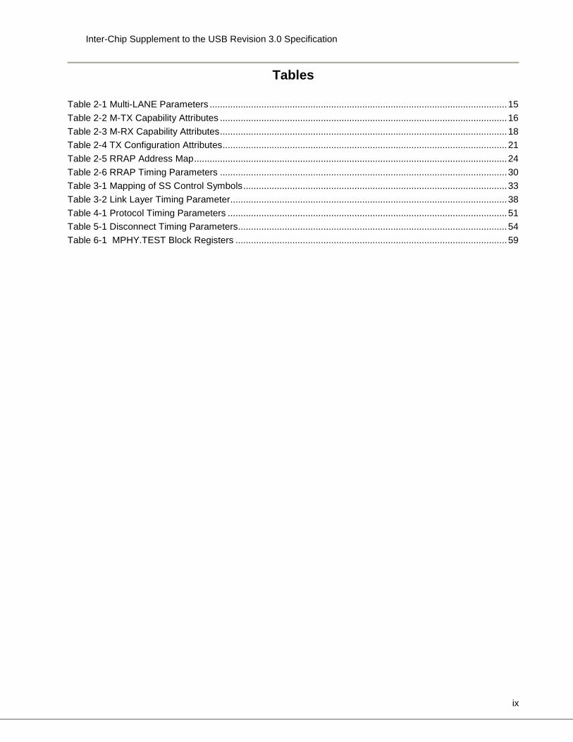
The SSIC Link Training and Status State Machine (LTSSM) of the link layer is shown in Figure 3-7. The 392 figure and following section documents relevant state details, associated transitions and details of the 393 mapping of the LTSSM state to the M-PHY state machines. 394
Unless otherwise noted, requirements for LTSSM states and sub-states defined in [USB 3.0] also apply 395 to this supplement and are not reproduced here. However [USB 3.0] LTSSM requirements 396 corresponding to the physical layer do not apply and instead M-PHY M-TX and M-RX requirements 397 detailed in this section shall be followed. Specifically Low Frequency Periodic Signaling (LFPS) and 398 Receiver Termination Detection and the various signaling mechanisms thereof do not apply to this 399 supplement. 400
Implementation Note: This section has been specified to allow compliant implementations to be designed using an existing [USB 3.0] compliant LTSSM and a suitable PA layer as shown in Figure 1-2. This does not imply preference for any particular style of implementation, and other implementations are supported, provided they comply to the requirements of this section.
401
Inter-Chip Supplement to the USB Revision 3.0 Specification
40
402
Figure 3-7 SSIC LTSSM state diagram 403 404
3.8.1 SS.Disabled 405
SS.Disabled is a logical power-off state when a port is unpowered or when the SSIC port’s functionality 406 is disabled. 407
A DSP when directed to do so shall signal a DSP disconnect and transition to this state. 408
3.8.1.1 SS.Disabled Requirements 409
The SS.Disabled state does not contain any sub-states as shown in Figure 3-8: 410
U3 ExitTimeout
Note: Figure is illustrative only. Not all of the transition conditions are listed. Refer to text for details.
USP Disconnect Detected (DSP only)M-RX: LINE-RESET
U0HS-BURST/STALL
U2HIBERN8
Hot ResetHS-BURST
PollingHS-BURST/STALL
Timeout
Rx.DetectSLEEP/PWM-BURST/
HIBERN8
Directed FromAny Other States
Power On Reset Assertion
U1STALL
RecoverySTALL/HS-BURST
U3HIBERN8
U3 Exit Handshake
Timeout
U2 ExitTimeout
Timeout
Directed
Training
Idle Symbol Handshake
LGO_U2
LGO_U3
Link Non-recoverable
Timeout(USP)Directed (DSP)
Directed
Error, Directed
Directed U1 ExitM-RX receives DIFF-P
LGO_U1
U2 Exit Handshake
LTSSM StateM-TX/M-RX State
SS.InactiveDISABLED/HIBERN8
DirectedUSP M-RX: Exiting HIBERN8
SS.DisabledDISABLED
Timeout (DSP)
Link/Protocol EventM-TX/M-RX Event
LEGEND
Training
Warm Reset(DSP & USP)LINE-RESET
Remote Link Partner Detected
M-RX: HIBERN8 Exit
USP Disconnect Signaled (USP only)M-TX: LINE-RESET
MPHY.TESTPWM-BURST
Test Mode detected in
PWM-BURST
Tester ResetLINE-RESET
Inter-Chip Supplement to the USB Revision 3.0 Specification
41
• The M-PHY local RESET to the M-RX and M-TX of all PAIRs shall be asserted which maintains 411 the modules in the DISABLED state 412
413
Figure 3-8 SS.Disabled state 414
3.8.1.2 Exit from SS.Disabled 415
• Exit shall take place for a USP via the deassertion of Power-On Reset and for a DSP when 416 directed to exit: 417
o The M-PHY local RESET to the M-RX and M-TX of all PAIRs shall be de-asserted which 418 transitions the modules from the DISABLED to the HIBERN8 state. 419
o the LTSSM shall transition to Rx.Detect.Active LTSSM state. 420
3.8.2 RX.Detect 421
The Rx.Detect state of the LTSSM is entered in the following scenarios: 422
• Signaling of a Warm Reset by a DSP 423 • Detection of a Warm Reset by a USP 424 • Detection of a USP disconnect by a DSP 425 • Completion of Power on Reset by both a DSP and USP 426 • When Polling or Recovery is unsuccessful for a DSP as defined in [USB 3.0] 427 • Signaling of a LINE-RESET by Test Equipment 428
The concept of far-end terminations as defined in [USB 3.0] does not apply to this supplement and 429 instead M-PHY based mechanisms shall be used to detect the presence of a link partner and to 430 synchronize operation as defined in this section. 431
Rx.Detect contains a sub-state machine as shown in Figure 3-9 with the following sub-states: 432
• Rx.Detect.Reset 433 • Rx.Detect.Active 434 • Rx.Detect.LS-MODE 435
436
SS.DisabledDISABLED
Power-On Reset Assertion, Directed
Exit to Rx.Detect
DSP: DirectedUSP: Power-On Reset deassertion
Note: Figure is illustrative only. Not all of the transition conditions are listed. Refer to text for details.
USP Disconnect Signaled (USP only)M-TX: LINE-RESET
Inter-Chip Supplement to the USB Revision 3.0 Specification
42
437
Figure 3-9 Rx.Detect Sub-state Machine 438
3.8.2.1 RX.Detect.Reset Requirements 439
This sub-state is entered in following scenarios: 440
• LINE-RESET signaled by a DSP as part of Warm Reset as defined in 3.6.2.2 (both USP and 441 DSP enter) or 442
• LINE-RESET is signaled during a USP disconnect as defined in Section 5.1.1(DSP only enters) 443 • LINE-RESET is signaled by Test Equipment 444
445
In this sub-state the USP and DSP shall complete the following steps in the following order: 446
• Wait for the completion of LINE-RESET signaling. 447 • Assert the local M-PHY Reset for all LANEs within Tline_to_local_rst bringing the M-TX and M-448
RX to the DISABLED state on all PAIRs. 449 • Keep local M-PHY Reset asserted for Tlocal_rst 450 • De-assert the local M-PHY Reset bringing the M-TX and M-RX to the HIBERN8 state on all 451
PAIRs. 452
In the case of a warm reset, a DSP may handle any delays in completion of the above steps by an USP 453 in an implementation-specific manner. 454
Rx.Detect.Reset DISABLED/HIBERN8
Exit to SS.Disabled
Directed (DSP only)
Exit to Polling
Rx.Detect.ActiveM-TX: SLEEP(DSP)/HIBERN8(USP)
M-RX: HIBERN8
M-RX: HIBERN8 exit
Warm Reset Completion
Warm Reset
USP Disconnect detected (DSP only)
Directed from SS.Disabled
Note: Figure is illustrative only. Not all of the transition conditions are listed. Refer to text for details.
Rx.Detect.LS-MODESLEEP/PWM-BURST
Exit to MPHY.TEST
Test mode detected in PWM-BURST
RCT
Inter-Chip Supplement to the USB Revision 3.0 Specification
43
3.8.2.2 Exit from RX.Detect.Reset 455
• A port shall transition to Rx.Detect.Active after completing the required steps as defined in 456 Section 3.8.2.1. 457
• A DSP shall transition to SS.Disabled when directed. 458
3.8.2.3 RX.Detect.Active Requirements 459
Rx.Detect.Active is a sub-state to detect the presence of a link partner. 460
• For a DSP: 461 • The M-TX shall be configured to exit HIBERN8 into the SLEEP state which results in a 462
DIF-N value being driven on all PAIRs. 463 • The M-RX shall remain in HIBERN8 on all PAIRs until the link partner initiates a 464
HIBERN8 exit 465 • For a USP: 466
• The M-TX and M-RX shall remain in HIBERN8 until the link partner initiates a HIBERN8 467 exit 468
3.8.2.4 Exit from RX.Detect.Active 469
• Upon detection of a HIBERN8 exit on its M-RX on any PAIR the USP shall initiate an exit from 470 HIBERN8 on its M-TX of all PAIRs and shall transition to Rx.Detect.LS-MODE. 471
• Upon detection of a HIBERN8 exit on its M-RX on all PAIRs the DSP shall wait a minimum 472 Tactivate time before transitioning to Rx.Detect.LS-MODE. 473
• A DSP shall transition to SS.Disabled when directed. 474
3.8.2.5 RX.Detect.LS-MODE Requirements 475
Rx.Detect.LS-MODE is a sub-state in which communication takes place in the LS-MODE using the 476 RRAP. 477
The requirements for this sub-state for a USP, DSP are defined in Section 2.5. 478
3.8.2.6 Exit from RX.Detect.LS-MODE 479
• A DSP shall transition to SS.Disabled when directed. 480 • An USP and a DSP shall exit to the MPHY.TEST state when an RRAP write command to the 481
TEST_MODE register is received as defined in Table 2-5. 482 • An USP and a DSP shall execute a RCT to exit this sub-state and enter Polling when configured 483
to do so using the RRAP as defined in Section 2.5.3. 484 • After executing an RCT, the M-TX shall wait for a period equal to the 485
RX_Min_ActivateTime_Capability defined in Section 2.2.3 prior to exiting this sub-state into the 486 Polling state. 487
• Note: A delay equivalent to the RX_Min_ActivateTime_Capability timing parameter is prescribed 488 in this sub-state to allow flexibility for implementations to prepare for STALL and HS-BURST. 489 490
3.8.3 Polling 491
In the Polling state the M-PHY is configured prior to entering HS-BURST. While in HS-BURST, the 492 training ordered sets of TS1, and TS2 as defined in [USB 3.0] are transmitted. 493
Polling contains a sub-state machine shown in Figure 3-10 with the following sub-states: 494
• Polling.STALL 495 • Polling.Active 496
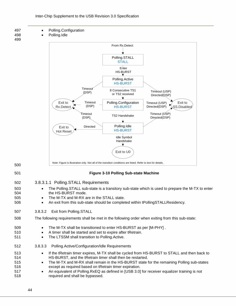
Inter-Chip Supplement to the USB Revision 3.0 Specification
44
• Polling.Configuration 497 • Polling.Idle 498
499
500
Figure 3-10 Polling Sub-state Machine 501
3.8.3.1.1 Polling.STALL Requirements 502 • The Polling.STALL sub-state is a transitory sub-state which is used to prepare the M-TX to enter 503
the HS-BURST mode. 504 • The M-TX and M-RX are in the STALL state. 505 • An exit from this sub-state should be completed within tPollingSTALLResidency. 506
3.8.3.2 Exit from Polling.STALL 507
The following requirements shall be met in the following order when exiting from this sub-state: 508
• The M-TX shall be transitioned to enter HS-BURST as per [M-PHY] . 509 • A timer shall be started and set to expire after tRetrain. 510 • The LTSSM shall transition to Polling.Active. 511
3.8.3.3 Polling.Active/Configuration/Idle Requirements 512
• If the tRetrain timer expires, M-TX shall be cycled from HS-BURST to STALL and then back to 513 HS-BURST, and the tRetrain timer shall then be restarted. 514
• The M-TX and M-RX shall remain in the HS-BURST state for the remaining Polling sub-states 515 except as required based on tRetrain timer expiration. 516
• An equivalent of Polling.RxEQ as defined in [USB 3.0] for receiver equalizer training is not 517 required and shall be bypassed. 518
Polling.STALLSTALL
From Rx.Detect
Enter HS-BURST
Polling.ActiveHS-BURST
Polling.ConfigurationHS-BURST
8 Consecutive TS1 or TS2 received
Polling.IdleHS-BURST
TS2 Handshake
Idle Symbol Handshake
Exit to U0
Exit to Hot Reset
Directed
Exit to Rx.Detect
Exit to SS.Disabled
Timeout(DSP)
Timeout(DSP)
Timeout(DSP)
Timeout (USP)Directed(DSP)
Timeout (USP)Directed(DSP)
Timeout (USP)Directed(DSP)
Note: Figure is illustrative only. Not all of the transition conditions are listed. Refer to text for details.
Inter-Chip Supplement to the USB Revision 3.0 Specification
45
• The Disabling Scrambling bit and the Loopback bit in the link configuration field of the TS2 519 Ordered Set shall be ignored. 520
• Upon successful completion of the Polling sub-states the LTSSM shall transition to U0. 521 • The requirements in these sub-states including the handshake sequences and transitions due to 522
the expiry of relevant timers are as defined in [USB 3.0], without regard to transitions through 523 STALL due to tRetrain timer expiration. 524
• Note: M-RX receiver bit synchronization and training is completed using mechanisms specified 525 in [M-PHY] . The supplement defines the tRetrain timer as a contingency to enable [M-PHY] 526 specific training mechanism to be re-performed. As a result, none of the 527 Polling.Active/Configuration/Idle Timeouts defined in [USB 3.0] are expected to expire in SSIC 528 implementations with correctly operating M-TX and M-RX modules. 529
3.8.4 U0 530
U0 is the normal operational state in which the M-TX and M-RX are in the HS-Burst state and are 531 actively transmitting and receiving traffic. U0 contains no sub-states. 532
While in U0 the M-TX and the M-RX of a PORT may independently transition between the HS-BURST 533 and STALL states as shown in Figure 3-11. 534
The M-TX may optionally transition to the STALL state instead of transmitting logical idle symbols. The 535 conditions under which this transition is made such as number of logical idle symbols that are 536 transmitted prior to entering the STALL state are not specified in this supplement. For example, 537 implementations may choose to transition to STALL immediately without transmitting any logical idle 538 symbols or may continue to transmit logical idle symbols without entering the STALL state. 539
Independently the M-RX shall transition to the STALL state when the link partner’s M-TX implementation 540 chooses to enter the STALL state. 541
Implementation Note:
In the implementation example described in Figure 1-2, when the PA detects a STALL entry on its M-RX while in U0, the PA may have to manufacture logical idle symbols to be sent to the link layer to maintain the U0 state in the legacy LTSSM.
542
3.8.4.1 Exit from U0 543
• A successful LGO_U1 entry sequence shall transition the link state to U1 and the M-TX/M-RX to 544 STALL as follows: 545
o The DSP shall initiate LGO_U1 and shall disable STALL entry on all PAIRs until a LXU 546 is received (indicating abort of U1 entry) or it successfully enters U1. 547
o The USP, upon receipt of the LGO_U1 and if accepting U1 entry, shall in the following 548 order: 549
disable STALL entry on all PAIRs until it successfully enters U1 550 respond with a LAU 551
o After sending an LPMA, the DSP shall transition to U1 and transition its M-TX to the 552 STALL state on all PAIRs. 553
o After receiving an LPMA, the USP shall transition to U1 and transition its M-TX to the 554 STALL state on all PAIRs. 555
o U1 can also be initiated by a USP in which case the above sequence takes place with 556 the roles of DSP and USP reversed. 557
• A successful LGO_U2/LGO_U3 entry sequence shall transition the link state to U2/U3 and the 558 M-TX/M-RX to HIBERN8 as follows: 559
o The DSP shall in the following order: 560
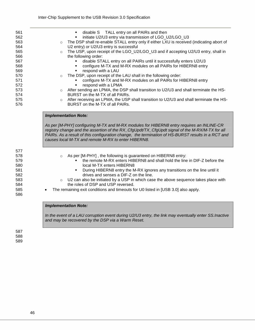
Inter-Chip Supplement to the USB Revision 3.0 Specification
46
disable S TALL entry on all PAIRs and then 561 initiate U2/U3 entry via transmission of LGO_U2/LGO_U3 562
o The DSP shall re-enable STALL entry only if either LXU is received (indicating abort of 563 U2 entry) or U2/U3 entry is successful 564
o The USP, upon receipt of the LGO_U2/LGO_U3 and if accepting U2/U3 entry, shall in 565 the following order: 566
disable STALL entry on all PAIRs until it successfully enters U2/U3 567 configure M-TX and M-RX modules on all PAIRs for HIBERN8 entry 568 respond with a LAU 569
o The DSP, upon receipt of the LAU shall in the following order: 570 configure M-TX and M-RX modules on all PAIRs for HIBERN8 entry 571 respond with a LPMA 572
o After sending an LPMA, the DSP shall transition to U2/U3 and shall terminate the HS-573 BURST on the M-TX of all PAIRs. 574
o After receiving an LPMA, the USP shall transition to U2/U3 and shall terminate the HS-575 BURST on the M-TX of all PAIRs. 576
Implementation Note:
As per [M-PHY] configuring M-TX and M-RX modules for HIBERN8 entry requires an INLINE-CR registry change and the assertion of the RX_CfgUpdt/TX_CfgUpdt signal of the M-RX/M-TX for all PAIRs. As a result of this configuration change, the termination of HS-BURST results in a RCT and causes local M-TX and remote M-RX to enter HIBERN8.
577 o As per [M-PHY] , the following is guaranteed on HIBERN8 entry: 578
the remote M-RX enters HIBERN8 and shall hold the line in DIF-Z before the 579 local M-TX enters HIBERN8 580
During HIBERN8 entry the M-RX ignores any transitions on the line until it 581 drives and senses a DIF-Z on the line. 582
o U2 can also be initiated by a USP in which case the above sequence takes place with 583 the roles of DSP and USP reversed. 584
• The remaining exit conditions and timeouts for U0 listed in [USB 3.0] also apply. 585 586
Implementation Note:
In the event of a LAU corruption event during U2/U3 entry, the link may eventually enter SS.Inactive and may be recovered by the DSP via a Warm Reset.
587 588 589
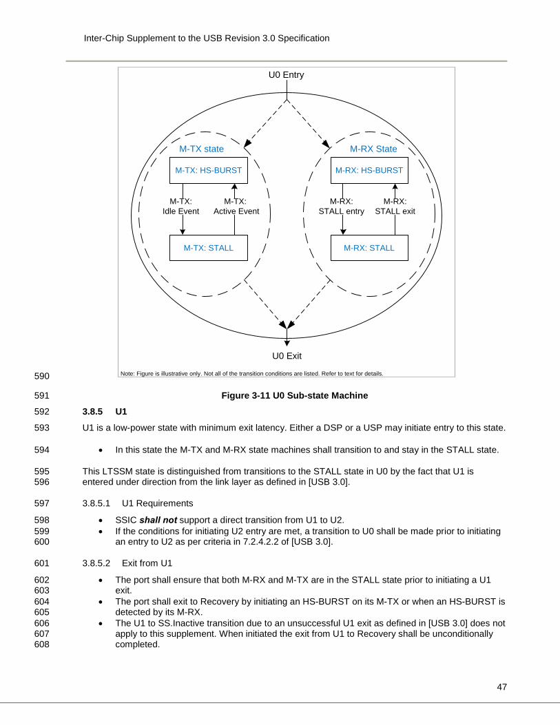
Inter-Chip Supplement to the USB Revision 3.0 Specification
47
590
Figure 3-11 U0 Sub-state Machine 591
3.8.5 U1 592
U1 is a low-power state with minimum exit latency. Either a DSP or a USP may initiate entry to this state. 593
• In this state the M-TX and M-RX state machines shall transition to and stay in the STALL state. 594
This LTSSM state is distinguished from transitions to the STALL state in U0 by the fact that U1 is 595 entered under direction from the link layer as defined in [USB 3.0]. 596
3.8.5.1 U1 Requirements 597
• SSIC shall not support a direct transition from U1 to U2. 598 • If the conditions for initiating U2 entry are met, a transition to U0 shall be made prior to initiating 599
an entry to U2 as per criteria in 7.2.4.2.2 of [USB 3.0]. 600
3.8.5.2 Exit from U1 601
• The port shall ensure that both M-RX and M-TX are in the STALL state prior to initiating a U1 602 exit. 603
• The port shall exit to Recovery by initiating an HS-BURST on its M-TX or when an HS-BURST is 604 detected by its M-RX. 605
• The U1 to SS.Inactive transition due to an unsuccessful U1 exit as defined in [USB 3.0] does not 606 apply to this supplement. When initiated the exit from U1 to Recovery shall be unconditionally 607 completed. 608
M-TX: HS-BURST
M-TX: STALL
U0 Entry
U0 Exit
M-TX state M-RX State
M-TX:Idle Event
M-TX: Active Event
M-RX: HS-BURST
M-RX: STALL
M-RX: STALL entry
M-RX: STALL exit
Note: Figure is illustrative only. Not all of the transition conditions are listed. Refer to text for details.
Inter-Chip Supplement to the USB Revision 3.0 Specification
48
609
3.8.6 U2 610
U2 is a link state where more power saving opportunities are allowed compared to U1, but with an 611 increased exit latency. U2 does not contain any sub-states. Either a DSP or a USP may initiate entry to 612 this state. 613
3.8.6.1 U2 Requirements 614
• The M-TX and the M-RX state machines shall stay in the HIBERN8 state for all PAIRs. 615 • The concept of far end receiver termination detection as defined in [USB 3.0] does not apply and 616
does not have to be completed while in this state. 617
3.8.6.2 Exit from U2 618
• The port shall transition to Recovery when a successful U2 exit handshake completes in the 619 following manner: 620
o The M-RX receives an HIBERN8 exit indication on all PAIRs or M-TX initiates a 621 HIBERN8 exit on all PAIRs when port is directed to exit U2 by the link layer and 622
o Both M-TX and M-RX successfully exit HIBERN8 on all PAIRs and transition to STALL. 623 • The port shall transition to SS.Inactive if the tNoLFPSResponseTimeout timer (as defined in 624
[USB 3.0]) expires and if a successful U2 exit handshake as described above is not achieved. 625
The following [M-PHY] capability attributes described in Section 2.2.3 imply a minimum residency of 626 200µs in U2: 627
• Rx/Tx_Hibern8Time_Capability = 100us: Minimum residency time in HIBERN8 state 628 • RX_Min_ActivateTime_Capability = 100us: Minimum time to exit HIBERN8 629
The SSIC LTSSM shall ensure that these residency requirements in [M-PHY] are met prior to initiating a 630 U2 exit. 631
632
Implementation Note:
[M-PHY] defines the RX_Advanced_Granularity_Capability attribute that enables implementations to advertise support for a minimum HIBERN8 residency time and an activate time in granularities smaller than 100us. DSP implementations may discover support for this capability via RRAP and if supported may use it to reduce the default minimum residency of 200 µs in U2.
633
3.8.7 U3 634
U3 is a link state where a device is put into a suspend state. Though both U2 and U3 map to HIBERN8, 635 U3 may provide additional power savings opportunities at a system level due to the requirement to 636 complete a handshake upon an exit. Details of such system-level power savings opportunities and the 637 means for enabling them are out of scope of this supplement. 638
U3 does not contain any sub-states. 639
3.8.7.1 U3 Requirements 640
• In this state the M-TX and M-RX state machines are in the HIBERN8 State for all PAIRs. 641
Inter-Chip Supplement to the USB Revision 3.0 Specification
49
• A port not able to respond to U3 exit handshake within tNoLFPSResponseTimeout (as defined in 642 [USB 3.0]) may respond when it is ready. 643
• The concept of far end receiver termination detection as defined in [USB 3.0] does not apply and 644 does not have to be completed while in this state. 645
3.8.7.2 Exit from U3 646
• The port shall transition to Recovery when a successful U3 exit handshake completes in the 647 following manner: 648
o One of the following initial conditions is true: 649 The M-TX drives a HIBERN8 exit on all PAIRs when the port is directed to exit 650
U3 by the link layer or 651 the M-RX receives a HIBERN8 exit indication on all PAIRs 652
o and the M-TX successfully exit HIBERN8 on all PAIRs and transitions to STALL for a 653 minimum of Tactivate 654
o and a minimum Tactivate time has elapsed after M-RX receives a HIBERN8 exit on all 655 PAIRs. 656
• The port shall remain in U3 when a successful U3 exit handshake as described above is not 657 achieved. 658
o In this case the M-TX which initiated the HIBERN8 exit shall continue to drive DIF-N until 659 the U3 exit handshake successfully completes. 660
• Implementations shall ensure that minimum HIBERN8 residency requirements in [M-PHY] are 661 met prior to initiating a U3 exit. 662 663
3.8.8 Recovery 664
Recovery is a LTSSM state that is entered to retrain the M-PORT. During this state TS1, and TS2 665 training ordered sets are transmitted as defined in [USB 3.0] to synchronize the link and to exchange the 666 link configuration information. 667
Recovery contains the following sub-states: 668
• Recovery.Active 669 • Recovery.Configuration 670 • Recovery.Idle 671
3.8.8.1 Recovery.Active Requirements 672
• A timer set to expire after tRecoveryActiveTimeout (as defined in [USB 3.0]) shall be started 673 upon entry to this sub-state. 674
• Initial conditions for this sub-state are dependent on the entry condition: 675 • When entered from U0, the M-TX shall be brought to a STALL state in order to re-train 676
the M-TX for a new HS-BURST. The M-RX state is dependent on the link partner M-TX. 677 • When entered from U1, the M-RX or M-TX shall initially be in the STALL state as per U1 678
requirements defined in 3.8.5.2. 679 • When entered from U2 or U3, the M-RX and M-TX are initially in the STALL state. 680
• The M-TX is then brought to the HS-BURST state and the port shall transmit the TS1 ordered 681 sets upon entry to this sub-state. 682
• Upon M-TX entry into HS-BURST, the LTSSM shall start a tRetrain timer. 683
3.8.8.2 Recovery.Active/Configuration/Idle Requirements 684
• If the tRetrain timer expires, M-TX shall be cycled from HS-BURST to STALL and then back to 685 HS-BURST, and the tRetrain timer shall then be restarted. 686
• The M-TX and M-RX shall remain in the HS-BURST state for the remaining Recovery sub-687 states, except as required based on tRetrain timer expiration. 688
Inter-Chip Supplement to the USB Revision 3.0 Specification
50
• The requirements for the traffic, handshake sequences and exit conditions for these sub-states 689 are as defined in [USB 3.0], without regard to transitions through STALL due to tRetrain timer 690 expiration. 691
• The Disabling Scrambling bit and the Loopback bit in the link configuration field of the TS2 692 Ordered Set shall be ignored. 693
• Upon successful completion of the Recovery sub-states the LTSSM shall transition to U0. 694
3.8.9 Hot Reset 695
The Hot Reset state shall be implemented as specified in [USB 3.0]. 696
3.8.9.1 Hot Reset Requirements 697
• In this state the M-TX and M-RX are in the HS-BURST state. 698 • The port shall implement the Hot Reset sub-states, associated timers and exit conditions as 699
defined in [USB 3.0]. 700
3.8.10 SS.Inactive 701
SS.Inactive is an error state where the link becomes non-operational. 702
A DSP in this state, shall transition its M-TX and M-RX to the DISABLED state. In this state, the DSP is 703 not able to receive any communication from the USP. A DSP shall only exit from this state when directed 704 to issue a Warm Reset. In order to signal a warm reset, the DSP shall transition out of the DISABLED 705 state and drive a LINE-RESET as defined in [M-PHY] on PAIR0. 706
An USP in this state, shall assert and then de-assert the local M-PHY Reset for all LANEs bringing the 707 M-TX and M-RX to the HIBERN8 state on all PAIRs. A USP shall only exit upon the receipt of a Warm 708 Reset. While in SS.Inactive an USP shall ignore any data received on the M-RX until a LINE-RESET is 709 received. 710
The concept of far end receiver termination detection as defined in [USB 3.0] does not apply and does 711 not have to be completed while in this state. 712
3.8.11 MPHY.TEST 713
MPHY.TEST is an LTSSM state used for testing the M-PHY Physical layer. 714
The initial state of the M-TX and M-RX state machines in this state is PWM-BURST. 715
For details of the operational behavior in this state please refer to Section 6. 716
717
Inter-Chip Supplement to the USB Revision 3.0 Specification
51
4 Protocol Layer 718
Implementations incorporate the protocol layer defined in [USB 3.0] except as defined in this section. 719
4.1 Port Capability Link Management Packet (LMP) 720
The Port Capability LMP describes each port's link capabilities and is sent by both link partners after the 721 successful completion of training and link initialization. 722
Implementations shall ignore the Link Speed field of the Port capability LMP. The operational speed of 723 the link shall be defined by the profile as defined in Section 2.2.1. 724
Implementations shall ignore the USB 3.0 OTG Capable (OTG) field of the Port Capability LMP. The 725 Direction (D) field shall be used to identify the DSP and the USP as defined in [USB 3.0]. 726
4.2 Timing Parameters 727
The protocol-layer timing parameters described in Section 8.13 of [USB 3.0] also apply to this 728 supplement. 729
However certain timing parameters are modified as shown in Table 4-1 to account for a slower bit-rate 730 (for HS-G1/G2) and latencies introduced due to STALL entry and exit while in U0. 731
This supplement also relaxes the accuracy of timestamps reported by Isochronous Timestamp Packets 732 in the following manner: The Delta value of the ITS field shall be required to have an accuracy of ±5 733 tIsochTimestampGranularity units. 734
Table 4-1 Protocol Timing Parameters 735
Name Description Min Max Units
tPingResponse Time between device reception of the last framing symbol of a ping and the first framing symbol of the ping_response
5000 ns
tNRDYorSTALLResponse Time between device reception of the last framing symbol for an ACK TP or a DPP or a STATUS TP and the first framing symbol of an NRDY or STALL response
5000 ns
tDPResponse Time between device reception of the last framing symbol for an ACK TP and the first framing symbol of a DP response
5000 ns
tACKResponse Time between device reception of the last framing symbol for a DPP or a STATUS TP and the first framing symbol of an ACK response
5000 ns
tMaxBurstInterval Time between DPs when the device or host is bursting. If the device cannot meet this maximum time, then it shall set the EOB flag in the last DP it sends.
1000 ns
Inter-Chip Supplement to the USB Revision 3.0 Specification
52
tHostACKResponse Time between host reception of the last framing symbol for a DPP and the first framing symbol of an ACK response
5000 ns
Inter-Chip Supplement to the USB Revision 3.0 Specification
53
5 Device Framework 736
Implementations incorporate the device framework defined in [USB 3.0] except as defined in this section. 737
5.1 Dynamic Attachment and Removal 738
Though this interconnect is intended for embedded inter-chip links, there is a usage requirement to 739 support dynamic removal and subsequent attachment to support power management goals or to present 740 an alternative device configuration. This supplement supports mechanisms to have either the USP or the 741 DSP initiate a disconnect as described in the following sections. 742
5.1.1 USP Disconnect 743
The use case for signaling an USP Disconnect is to enable a peripheral to re-enumerate with a different 744 device configuration. A USP achieves this by indicating a disconnect and a subsequent re-connect as 745 defined in this section. 746
The operational model for a USP to signal a Disconnect is as follows: 747
• The USP shall signal a Disconnect by signaling a LINE-RESET on its M-TX on PAIR0. 748 • The USP shall maintain a DIF-N prior to driving a DIF-P on its M-TX as per the LINE-RESET 749
timing specified in [M-PHY] . 750 • Signaling a LINE-RESET on any M-TX other than that of PAIR0 has undefined results. 751 • Upon completion of the LINE-RESET, the USP shall assert local M-PHY Reset for all LANEs 752
within Tline_to_local_rst 753 • The USP shall keep local M-PHY Reset asserted for Tlocal_rst 754 • The USP M-TX and M-RX of all the LANES shall subsequently transition to the DISABLED state 755 • The USP LTSSM shall transition to the SS.Disabled state. 756 • The Peripheral Upstream Device port shall transition to USDPORT.Powered-Off (as defined in 757
Fig 10-25 of [USB 3.0]). 758 • If a USP is in U3, a U3 exit handshake shall be completed prior to signaling a disconnect. 759
Signaling of a USP disconnect while in U3 is not supported and has undefined results. 760
The operational model for a DSP upon detecting a USP Disconnect is as follows: 761
• The DSP shall wait until the completion of LINE-RESET signaling 762 • Upon completion of the LINE-RESET, the DSP shall assert local M-PHY Reset for all LANEs 763
within Tline_to_local_rst 764 • The DSP shall keep local M-PHY Reset asserted for Tlocal_rst 765 • The DSP shall then transition to Rx.Detect.Active as described in Section 3.8.2 in order to detect 766
a subsequent re-connect from the USP. 767
The operational model for a USP to signal a subsequent re-connect is as follows: 768
• When ready to re-connect, the USP shall de-assert local M-PHY Reset on all LANEs. 769 • The USP M-TX and M-RX shall transition to the HIBERN8 state for all LANEs. 770 • The USP LTSSM shall transition to the Rx.Detect.Active state. 771 • The Peripheral Upstream Device port shall transition to USDPORT.Powered On (as defined in 772
Fig 10-25 of [USB 3.0]). 773
5.1.2 DSP Disconnect 774
The DSP disconnect is a host-initiated mechanism to enable a peripheral to re-enumerate with a 775 different device configuration. 776
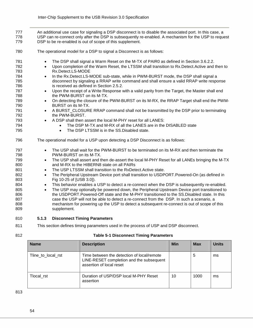
Inter-Chip Supplement to the USB Revision 3.0 Specification
54
An additional use case for signaling a DSP disconnect is to disable the associated port. In this case, a 777 USP can re-connect only after the DSP is subsequently re-enabled. A mechanism for the USP to request 778 DSP to be re-enabled is out of scope of this supplement. 779
The operational model for a DSP to signal a Disconnect is as follows: 780
• The DSP shall signal a Warm Reset on the M-TX of PAIR0 as defined in Section 3.6.2.2. 781 • Upon completion of the Warm Reset, the LTSSM shall transition to Rx.Detect.Active and then to 782
Rx.Detect.LS-MODE 783 • In the Rx.Detect.LS-MODE sub-state, while in PWM-BURST mode, the DSP shall signal a 784
disconnect by signaling a RRAP write command and shall ensure a valid RRAP write response 785 is received as defined in Section 2.5.2. 786
• Upon the receipt of a Write Response with a valid parity from the Target, the Master shall end 787 the PWM-BURST on its M-TX. 788
• On detecting the closure of the PWM-BURST on its M-RX, the RRAP Target shall end the PWM-789 BURST on its M-TX. 790
• A BURST_CLOSURE RRAP command shall not be transmitted by the DSP prior to terminating 791 the PWM-BURST. 792
• A DSP shall then assert the local M-PHY reset for all LANES: 793 • The DSP M-TX and M-RX of all the LANES are in the DISABLED state 794 • The DSP LTSSM is in the SS.Disabled state. 795
The operational model for a USP upon detecting a DSP Disconnect is as follows: 796
• The USP shall wait for the PWM-BURST to be terminated on its M-RX and then terminate the 797 PWM-BURST on its M-TX. 798
• The USP shall assert and then de-assert the local M-PHY Reset for all LANEs bringing the M-TX 799 and M-RX to the HIBERN8 state on all PAIRs 800
• The USP LTSSM shall transition to the RxDetect.Active state. 801 • The Peripheral Upstream Device port shall transition to USDPORT.Powered-On (as defined in 802
Fig 10-25 of [USB 3.0]). 803 • This behavior enables a USP to detect a re-connect when the DSP is subsequently re-enabled. 804 • The USP may optionally be powered down, the Peripheral Upstream Device port transitioned to 805
the USDPORT.Powered-Off state and the M-PHY transitioned to the SS.Disabled state. In this 806 case the USP will not be able to detect a re-connect from the DSP. In such a scenario, a 807 mechanism for powering up the USP to detect a subsequent re-connect is out of scope of this 808 supplement. 809
5.1.3 Disconnect Timing Parameters 810
This section defines timing parameters used in the process of USP and DSP disconnect. 811
Table 5-1 Disconnect Timing Parameters 812
Name Description Min Max Units
Tline_to_local_rst Time between the detection of local/remote LINE-RESET completion and the subsequent assertion of local reset
5 ms
Tlocal_rst Duration of USP/DSP local M-PHY Reset assertion
10 1000 ms
813
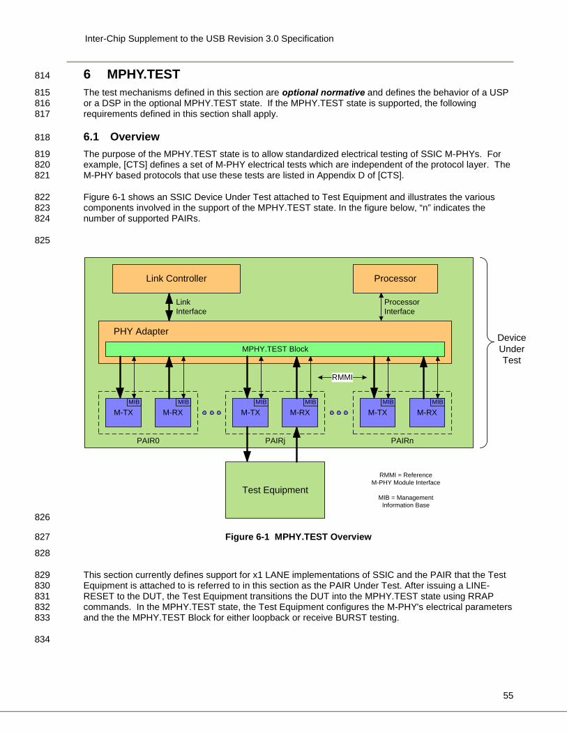
Inter-Chip Supplement to the USB Revision 3.0 Specification
55
6 MPHY.TEST 814
The test mechanisms defined in this section are optional normative and defines the behavior of a USP 815 or a DSP in the optional MPHY.TEST state. If the MPHY.TEST state is supported, the following 816 requirements defined in this section shall apply. 817
6.1 Overview 818
The purpose of the MPHY.TEST state is to allow standardized electrical testing of SSIC M-PHYs. For 819 example, [CTS] defines a set of M-PHY electrical tests which are independent of the protocol layer. The 820 M-PHY based protocols that use these tests are listed in Appendix D of [CTS]. 821
Figure 6-1 shows an SSIC Device Under Test attached to Test Equipment and illustrates the various 822 components involved in the support of the MPHY.TEST state. In the figure below, “n” indicates the 823 number of supported PAIRs. 824
825
826
Figure 6-1 MPHY.TEST Overview 827
828
This section currently defines support for x1 LANE implementations of SSIC and the PAIR that the Test 829 Equipment is attached to is referred to in this section as the PAIR Under Test. After issuing a LINE-830 RESET to the DUT, the Test Equipment transitions the DUT into the MPHY.TEST state using RRAP 831 commands. In the MPHY.TEST state, the Test Equipment configures the M-PHY's electrical parameters 832 and the the MPHY.TEST Block for either loopback or receive BURST testing. 833
834
Test Equipment
Test Equipment
Link Controller
M-RXM-TX
LinkInterface
MPHY.TEST Block
Processor
MIBMIB
RMMI
M-RXM-TXMIBMIB
PAIR0 PAIRn
PHY Adapter
ProcessorInterface
M-RXM-TXMIBMIB
PAIRj
Device Under Test
RMMI = Reference M-PHY Module Interface
MIB = Management Information Base
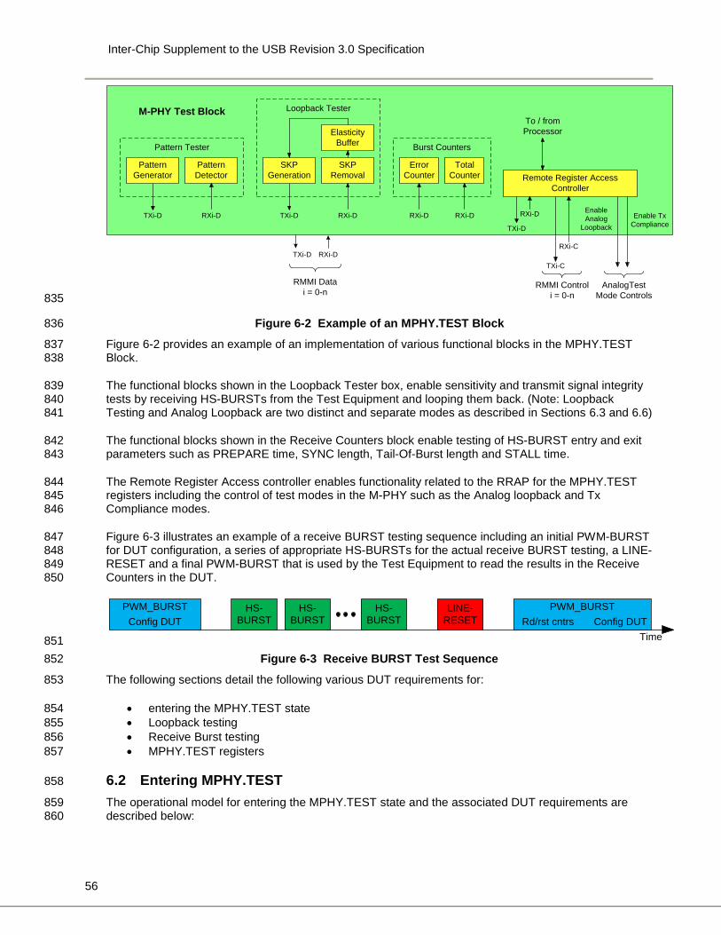
Inter-Chip Supplement to the USB Revision 3.0 Specification
56
835
Figure 6-2 Example of an MPHY.TEST Block 836
Figure 6-2 provides an example of an implementation of various functional blocks in the MPHY.TEST 837 Block. 838
The functional blocks shown in the Loopback Tester box, enable sensitivity and transmit signal integrity 839 tests by receiving HS-BURSTs from the Test Equipment and looping them back. (Note: Loopback 840 Testing and Analog Loopback are two distinct and separate modes as described in Sections 6.3 and 6.6) 841
The functional blocks shown in the Receive Counters block enable testing of HS-BURST entry and exit 842 parameters such as PREPARE time, SYNC length, Tail-Of-Burst length and STALL time. 843
The Remote Register Access controller enables functionality related to the RRAP for the MPHY.TEST 844 registers including the control of test modes in the M-PHY such as the Analog loopback and Tx 845 Compliance modes. 846
Figure 6-3 illustrates an example of a receive BURST testing sequence including an initial PWM-BURST 847 for DUT configuration, a series of appropriate HS-BURSTs for the actual receive BURST testing, a LINE-848 RESET and a final PWM-BURST that is used by the Test Equipment to read the results in the Receive 849 Counters in the DUT. 850
851 Figure 6-3 Receive BURST Test Sequence 852
The following sections detail the following various DUT requirements for: 853
• entering the MPHY.TEST state 854 • Loopback testing 855 • Receive Burst testing 856 • MPHY.TEST registers 857
6.2 Entering MPHY.TEST 858
The operational model for entering the MPHY.TEST state and the associated DUT requirements are 859 described below: 860
RXi-D
M-PHY Test Block
TXi-D
TXi-D
TXi-C
RXi-D
RXi-C
Elasticity Buffer
SKP Removal
SKP Generation
To / from Processor
Remote Register Access Controller
TXi-D RXi-D
RMMI Datai = 0-n
RMMI Controli = 0-n
Loopback Tester
RXi-D
Total Counter
Burst Counters
RXi-D
Error Counter
RXi-DTXi-D
Pattern Detector
Pattern Generator
Pattern Tester
Enable Analog
Loopback Enable Tx
Compliance
AnalogTest Mode Controls
HS-BURST
HS-BURST
LINE-RESET
PWM_BURSTConfig DUT
PWM_BURSTConfig DUTRd/rst cntrs
HS-BURST
Time
Inter-Chip Supplement to the USB Revision 3.0 Specification
57
• The DUT shall transition through the Rx.Detect.Reset, Rx.Detect.Active and the Rx.Detect.LS-861 MODE states as described in Section 3.8.2. 862
• In the Rx.Detect.LS-MODE state, the DUT shall support the receipt of a PWM-BURST from the Test 863 Equipment on any of the supported PAIRs. 864
• In the PWM-BURST mode, the DUT shall support the receipt of a RRAP Write Command to enable 865 the transition to the MPHY.TEST state and shall issue a valid Write Response as defined in Table 866 2-5. 867
• The DUT shall transition to the MPHY.TEST state. 868
6.3 Loopback Testing 869
The operational model for enabling Loopback Testing and the associated DUT requirements are 870 described below: 871
• Test equipment transitions the DUT to the MPHY.TEST mode prior to configuring it for Loopback 872 Testing. 873
• Test Equipment issues a RRAP Write Command to set the LOOPBACK_EN[0] register bit as 874 defined in Table 6-1. 875
• Upon receipt of the Write command, the DUT shall enable Loopback Testing for the PAIR under 876 Test and shall issue a valid Write Response. 877
• Test Equipment appropriately configures the PAIR under Test for HS-MODE. 878 • Test Equipment closes the PWM-BURST and ensures conditions are met for a RCT to transition the 879
DUT to the HS-MODE. A BURST_CLOSURE RRAP command is not required prior to terminating 880 the PWM-BURST. 881
• Upon detecting the start of HS-BURST on M-RX, the DUT stall initiate a HS-BURST on the M-TX 882 • Upon detecting the end of HS-BURST on M-RX, the DUT shall terminate the HS-BURST on the M-883
TX. 884 • Upon initiating a HS-BURST on the M-TX of the PAIR under Test, the DUT shall loop back received 885
HS-BURST payloads until a LINE-RESET is received. 886 • The DUT shall transmit the payload exactly as received with the exception of inserted or removed 887
SKP ordered sets, regardless of whether scrambling is enabled or disabled by the Tester Equipment 888 using the corresponding RRAP command. 889
• Upon initiating a HS-BURST on the M-TX of the PAIR under Test, the DUT may insert one or more 890 MK0 or FLR symbols until the loop back begins. 891
• Both M-RX and M-TX shall use the Configuration Attribute values as programmed using RRAP. 892 893
The following additional requirements for the PAIR under Test shall apply during Loopback Testing: 894
• The M-TX shall maintain running disparity of transmitted symbols. 895 • The PAIR is allowed to discard received SKP ordered sets in order to avoid receiver overflow 896 • The PAIR is allowed to inject SKP ordered sets in the transmitted data to avoid transmit underflow 897 • The M-TX shall close the HS-BURST when a HS-BURST closure is detected on the M-RX. 898
899 Upon detecting the start of an HS-BURST at the M-RX, the M-TX shall start output a HS-BURST. If the 900 PREPARE and SYNC period received on the M-RX is longer than the corresponding values in the M-TX, 901 the M-TX may inject SKP ordered sets after the initial MK0 of the transmit payload. If the PREPARE and 902 SYNC period received on the M-RX is shorter than the corresponding values in the M-TX, the M-TX may 903 drop symbols after the initial MK0 of the received payload. Test Equipment can ensure that the 904 PREPARE and SYNC period received on the M-RX is equal or greater than the corresponding values in 905 the M-TX, to prevent the dropping of symbols by the PAIR under Test. 906
Inter-Chip Supplement to the USB Revision 3.0 Specification
58
The size of the Elasticity Buffer shown in Figure 6-2 shall be sufficient to handle the maximum clock 907 skew allowed by [M-PHY] between two M-PORTs, given that the Test Equipment is required to inject at 908 least one SKP every 354 symbols. 909
910 6.4 Receive Burst Testing 911
The following requirements shall apply during Receive Burst Testing: 912
• The DUT shall implement the RX_BURST_COUNT, RX_ERR_COUNT and the 913 RX_COUNT_RESET registers as defined in Table 6-1. 914
• The RX_BURST_COUNT registers shall increment each time the M-RX of the PAIR under Test 915 transitions from HS-BURST to STALL. 916
• The four RX_BURST_COUNT registers implement a 4 Byte counter for the PAIR under Test 917 with RX_BURST_COUNT_0 indicating the LSB and RX_BURST_COUNT_3 the MSB of the 918 count. 919
• The RX_ERR_COUNT registers shall increment each time the M-RX of the PAIR under Test 920 transitions from HS-BURST to STALL without detecting an MK0 during the burst. 921
• The four RX_ERR_COUNT registers implement a 4 Byte counter for the PAIR under Test with 922 RX_ERR_COUNT_0 indicating the LSB and RX_ERR_COUNT_3 the MSB of the count. 923
• The RX_BURST_COUNT and RX_ERR_COUNT registers shall be reset when the DUT 924 receives a RRAP Write Command that sets the RX_COUNT_RESET[0] register. These registers 925 shall not be reset upon the receipt of a LINE-RESET. 926
• The RX_BURST_COUNT and RX_ERR_COUNT registers shall remain unchanged and not 927 rollover when they have reached their maximum values. 928
• The RX_BURST_COUNT and RX_ERR_COUNT registers shall always be updated as 929 described above when in the MPHY.TEST state. 930
6.5 Tx Compliance Mode 931
The operational model for enabling Tx Compliance mode and the associated DUT requirements are 932 described below: 933
• Test equipment transitions the DUT to the MPHY.TEST mode prior to configuring it in Tx 934 Compliance Mode. 935
• Test Equipment issues a RRAP Write Command to set the TX_COMP_MODE_EN[0] register bit 936 as defined in Table 6-1. 937
• Upon receipt of the Write command, the DUT shall enable Tx Compliance mode for the PAIR 938 under Test and shall issue a valid Write Response. 939
• Test Equipment appropriately configures the PAIR under Test for HS-MODE. 940 • Test Equipment closes the PWM-BURST on the M-RX of the PAIR under Test. A 941
BURST_CLOSURE RRAP command is not required prior to terminating the PWM-BURST. 942 • Upon detecting the end of PWM-BURST on its M-RX, the DUT shall terminate the PWM-BURST 943
on the M-TX. 944 • The M-TX of the PAIR under Test shall then continuously transmit the CRPAT compliance 945
pattern in HS-MODE as defined in [M-PHY] Annex B.1.2. 946 • The DUT shall remain in the Tx Compliance Mode until a LINE-RESET is received from the Test 947
Equipment. 948
6.6 Analog Loopback Mode 949
The operational model for enabling Analog Loopback mode and the associated DUT requirements are 950 described below: 951
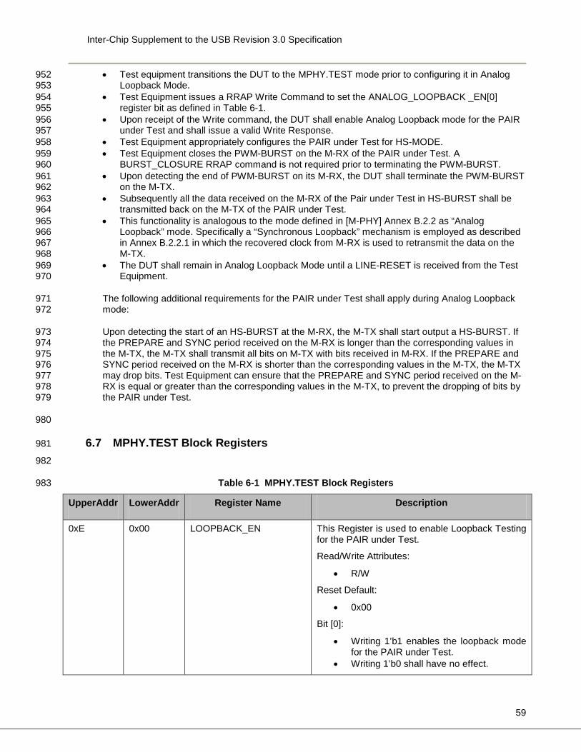
Inter-Chip Supplement to the USB Revision 3.0 Specification
59
• Test equipment transitions the DUT to the MPHY.TEST mode prior to configuring it in Analog 952 Loopback Mode. 953
• Test Equipment issues a RRAP Write Command to set the ANALOG_LOOPBACK _EN[0] 954 register bit as defined in Table 6-1. 955
• Upon receipt of the Write command, the DUT shall enable Analog Loopback mode for the PAIR 956 under Test and shall issue a valid Write Response. 957
• Test Equipment appropriately configures the PAIR under Test for HS-MODE. 958 • Test Equipment closes the PWM-BURST on the M-RX of the PAIR under Test. A 959
BURST_CLOSURE RRAP command is not required prior to terminating the PWM-BURST. 960 • Upon detecting the end of PWM-BURST on its M-RX, the DUT shall terminate the PWM-BURST 961
on the M-TX. 962 • Subsequently all the data received on the M-RX of the Pair under Test in HS-BURST shall be 963
transmitted back on the M-TX of the PAIR under Test. 964 • This functionality is analogous to the mode defined in [M-PHY] Annex B.2.2 as “Analog 965
Loopback” mode. Specifically a “Synchronous Loopback” mechanism is employed as described 966 in Annex B.2.2.1 in which the recovered clock from M-RX is used to retransmit the data on the 967 M-TX. 968
• The DUT shall remain in Analog Loopback Mode until a LINE-RESET is received from the Test 969 Equipment. 970
The following additional requirements for the PAIR under Test shall apply during Analog Loopback 971 mode: 972
Upon detecting the start of an HS-BURST at the M-RX, the M-TX shall start output a HS-BURST. If 973 the PREPARE and SYNC period received on the M-RX is longer than the corresponding values in 974 the M-TX, the M-TX shall transmit all bits on M-TX with bits received in M-RX. If the PREPARE and 975 SYNC period received on the M-RX is shorter than the corresponding values in the M-TX, the M-TX 976 may drop bits. Test Equipment can ensure that the PREPARE and SYNC period received on the M-977 RX is equal or greater than the corresponding values in the M-TX, to prevent the dropping of bits by 978 the PAIR under Test. 979
980
6.7 MPHY.TEST Block Registers 981
982
Table 6-1 MPHY.TEST Block Registers 983
UpperAddr LowerAddr Register Name Description
0xE 0x00 LOOPBACK_EN This Register is used to enable Loopback Testing for the PAIR under Test.
Read/Write Attributes:
• R/W
Reset Default:
• 0x00
Bit [0]:
• Writing 1’b1 enables the loopback mode for the PAIR under Test.
• Writing 1’b0 shall have no effect.
Inter-Chip Supplement to the USB Revision 3.0 Specification
60
UpperAddr LowerAddr Register Name Description
Once the bit is set, it shall only be reset via a LINE-RESET issued by Test Equipment.
Bit[7:1] Reserved.
• Writes shall be ignored and Reads shall return zero values.
0xE 0x01-0x04 RX_BURST_COUNT_0 RX_BURST_COUNT_1 RX_BURST_COUNT_2 RX_BURST_COUNT_3
These Registers count the number of bursts by incrementing on each HS-BURST to STALL transition. RX_BURST_COUNT_0 is the LSB.
R/W attributes:
• Read Only
Reset Default:
• 0x00
This register shall be reset only when RX_COUNT_RESET[0] is set. This register is not affected by a LINE-RESET issued by Test Equipment.
0xE 0x05-0x08 RX_ERR_COUNT_0 RX_ERR_COUNT_1 RX_ERR_COUNT_2 RX_ERR_COUNT_3
These Registers count the number of errors by incrementing on each HS-BURST to STALL transition for which an MK0 was not detected. RX_ERR_COUNT_0 is the LSB.
R/W attributes:
• Read Only
Reset Default:
• 0x00
This register shall be reset only when RX_COUNT_RESET[0] is set. This register is not affected by a LINE-RESET issued by Test Equipment.
0xE 0x09 RX_COUNT_RESET This register is used to reset the RX_BURST_COUNT and the RX_ERR_COUNT registers
R/W attributes:
• Write Only, Self Clearing
Reset Default:
• 0x00
Bit [0]:
Inter-Chip Supplement to the USB Revision 3.0 Specification
61
UpperAddr LowerAddr Register Name Description
• Writing 1’b1 resets the RX_BURST_COUNT and the RX_ERR_COUNT registers
Bits [7:1]: Reserved.
0xE 0x0A TX_COMP_MODE_EN This register is used to enable M-TX of the PAIR under Test in TX Compliance mode.
Writes to this register are undefined unless the DUT is in the MPHY.TEST state.
R/W Attributes:
• Write Only
Reset Default:
• 0x00
Bit [0]:
• Writing 1’b1 enables Tx Compliance Mode for the PAIR under Test. In this mode the DUT transmits the Continuous mode CRPAT defined in [CTS].
• Writing 1’b0 shall be ignored and Reads shall return zero values.
Once the bit is set, it shall only be reset via a LINE-RESET issued by Test Equipment.
Bits[7:1] Reserved:
• Writes shall be ignored and Reads shall return zero values.
0xE 0x0B ANALOG_LOOPBACK_EN This register is used to place the M-RX of the PAIR under Test in Analog Loopback mode.
Writes to this register are undefined unless the DUT is in the MPHY.TEST state.
R/W Attributes:
• Write Only
Reset Default:
• 0x00
Bit [0]:
• Writing 1’b1 enables Analog Loopback Mode for the PAIR under Test
• Writing 1’b0 shall be ignored and Reads shall return zero values.
Once the bit is set, it shall only be reset via a LINE-RESET issued by Test Equipment.
Bits[7:1] Reserved:
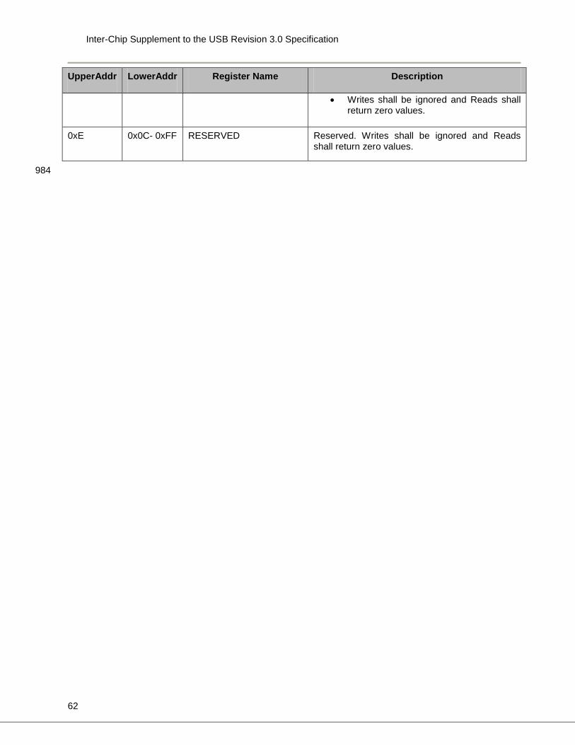
Inter-Chip Supplement to the USB Revision 3.0 Specification
62
UpperAddr LowerAddr Register Name Description
• Writes shall be ignored and Reads shall return zero values.
0xE 0x0C- 0xFF RESERVED Reserved. Writes shall be ignored and Reads shall return zero values.
984
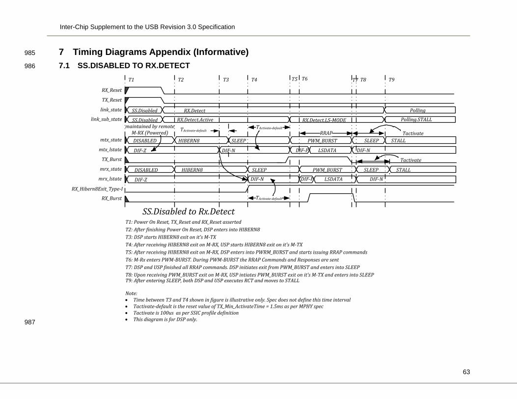
Inter-Chip Supplement to the USB Revision 3.0 Specification
63
7 Timing Diagrams Appendix (Informative) 985
7.1 SS.DISABLED TO RX.DETECT 986
987
T1 T2 T3 T4 T5 T6 T7 T8 T9
DIF-Z DIF-N
DISABLED HIBERN8 SLEEP PWM_BURST
DIF-Z DIF-N
SS.Disabled RX.Detect
DISABLED HIBERN8 SLEEP PWM_BURST
SS.Disabled to Rx.Detect
SLEEP STALL
SLEEP STALL
T1: Power On Reset, TX_Reset and RX_Reset assertedT2: After finishing Power On Reset, DSP enters into HIBERN8 T3: DSP starts HIBERN8 exit on it's M-TXT4: After receiving HIBERN8 exit on M-RX, USP starts HIBERN8 exit on it's M-TXT5: After receiving HIBERN8 exit on M-RX, DSP enters into PWRM_BURST and starts issuing RRAP commandsT6: M-Rx enters PWM-BURST. During PWM-BURST the RRAP Commands and Responses are sentT7: DSP and USP finished all RRAP commands. DSP initiates exit from PWM_BURST and enters into SLEEPT8: Upon receiving PWM_BURST exit on M-RX, USP intiates PWM_BURST exit on it's M-TX and enters into SLEEPT9: After entering SLEEP, both DSP and USP executes RCT and moves to STALL
Note: • Time between T3 and T4 shown in figure is illustrative only. Spec does not define this time interval• Tactivate-default is the reset value of TX_Min_ActivateTime = 1.5ms as per MPHY spec• Tactivate is 100us as per SSIC profile definition• This diagram is for DSP only.
DIF-P LSDATA DIF-N
DIF-P LSDATA DIF-N
RX_Reset
TX_Reset
link_state
mtx_state
mtx_lstate
TX_Burst
mrx_state
mrx_lstate
RX_Hibern8Exit_Type-I
RX_Burst
TActivate-defaultRRAP
SS.Disabled RX.Detect.Activelink_sub_state RX.Detect.LS-MODE Polling.STALL
Polling
Tactivate
Tactivate
TActivate-default
TActivate-defaultmaintained by remote
M-RX (Powered)
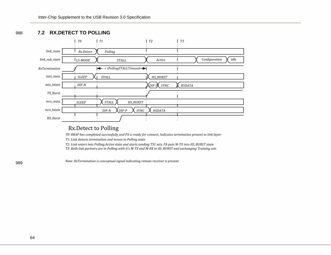
Inter-Chip Supplement to the USB Revision 3.0 Specification
64
7.2 RX.DETECT TO POLLING 988
989
T0 T1 T2 T3
DIF-N DIF-P SYNC HSDATA
STALL HS_BURST
DIF-N DIF-P SYNC HSDATA
STALL Active Configuration Idle
Rx.Detect Polling
STALL HS_BURST
Rx.Detect to PollingT0: RRAP has completed successfully and PA is ready for connect, Indicates termination present to link layer.T1: Link detects termination and moves to Polling stateT2: Link enters into Polling.Active state and starts sending TS1 sets, PA puts M-TX into HS_BURST stateT3: Both link partners are in Polling with it's M-TX and M-RX in HS_BURST and exchanging Training sets
Note: RxTermination is conceptual signal indicating remote receiver is present
link_state
RxTermination
link_sub_state
mtx_state
mtx_lstate
TX_Burst
mrx_state
mrx_lstate
RX_Burst
SLEEP
SLEEP
LS-MODE
< tPollingSTALLTimeout
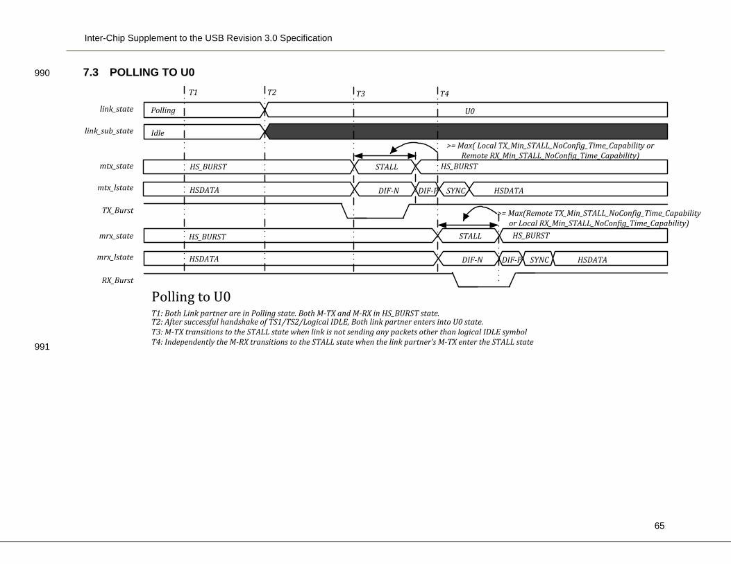
Inter-Chip Supplement to the USB Revision 3.0 Specification
65
7.3 POLLING TO U0 990
991
T1 T2
HSDATA
HS_BURST
Idle
Polling U0
Polling to U0T1: Both Link partner are in Polling state. Both M-TX and M-RX in HS_BURST state.T2: After successful handshake of TS1/TS2/Logical IDLE, Both link partner enters into U0 state.T3: M-TX transitions to the STALL state when link is not sending any packets other than logical IDLE symbolT4: Independently the M-RX transitions to the STALL state when the link partner’s M-TX enter the STALL state
link_state
link_sub_state
mtx_state
mrx_state
mtx_lstate
mrx_lstate
TX_Burst
RX_Burst
DIF-P SYNC HSDATA
STALL HS_BURSTHS_BURST
HSDATA DIF-N
DIF-P SYNC HSDATA
STALL HS_BURST
DIF-N
T3 T4
>= Max(Remote TX_Min_STALL_NoConfig_Time_Capability or Local RX_Min_STALL_NoConfig_Time_Capability)
>= Max( Local TX_Min_STALL_NoConfig_Time_Capability or Remote RX_Min_STALL_NoConfig_Time_Capability)
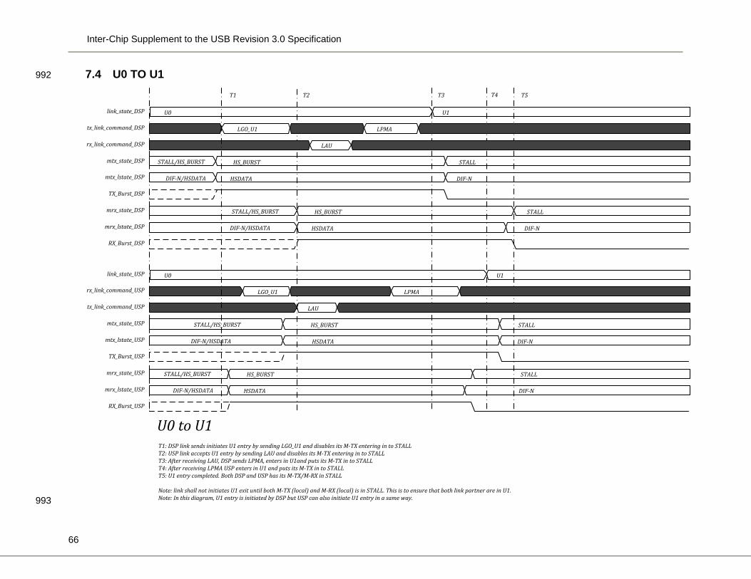
Inter-Chip Supplement to the USB Revision 3.0 Specification
66
7.4 U0 TO U1 992
993
T1 T2 T3 T4 T5
LGO_U1 LPMA
HSDATA DIF-N
HS_BURST STALL
HSDATA DIF-N
LAU
U0 U1
HS_BURST STALL
U0 to U1
LGO_U1 LPMA
HSDATA DIF-N
HS_BURST STALL
HSDATA DIF-N
LAU
U0 U1
HS_BURST STALL
T1: DSP link sends initiates U1 entry by sending LGO_U1 and disables its M-TX entering in to STALLT2: USP link accepts U1 entry by sending LAU and disables its M-TX entering in to STALLT3: After receiving LAU, DSP sends LPMA, enters in U1and puts its M-TX in to STALLT4: After receiving LPMA USP enters in U1 and puts its M-TX in to STALLT5: U1 entry completed. Both DSP and USP has its M-TX/M-RX in STALL
Note: link shall not initiates U1 exit until both M-TX (local) and M-RX (local) is in STALL. This is to ensure that both link partner are in U1.Note: In this diagram, U1 entry is initiated by DSP but USP can also initiate U1 entry in a same way.
STALL/HS_BURST
DIF-N/HSDATA
STALL/HS_BURST
DIF-N/HSDATA
STALL/HS_BURST
DIF-N/HSDATA
STALL/HS_BURST
DIF-N/HSDATA
link_state_DSP
tx_link_command_DSP
rx_link_command_DSP
mtx_state_DSP
mtx_lstate_DSP
TX_Burst_DSP
mrx_state_DSP
mrx_lstate_DSP
RX_Burst_DSP
link_state_USP
rx_link_command_USP
tx_link_command_USP
mtx_state_USP
mtx_lstate_USP
TX_Burst_USP
mrx_state_USP
mrx_lstate_USP
RX_Burst_USP
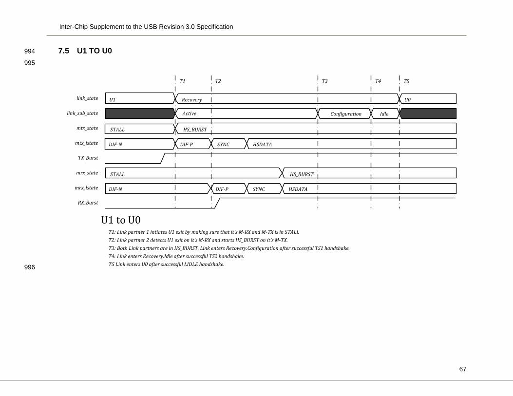
Inter-Chip Supplement to the USB Revision 3.0 Specification
67
7.5 U1 TO U0 994
995
996
T1 T2 T3 T4 T5
DIF-N DIF-P SYNC HSDATA
STALL HS_BURST
DIF-N DIF-P SYNC HSDATA
Active Configuration
U1 Recovery U0
STALL HS_BURST
U1 to U0T1: Link partner 1 intiates U1 exit by making sure that it's M-RX and M-TX is in STALLT2: Link partner 2 detects U1 exit on it's M-RX and starts HS_BURST on it's M-TX. T3: Both Link partners are in HS_BURST. Link enters Recovery.Configuration after successful TS1 handshake.T4: Link enters Recovery.Idle after successful TS2 handshake.T5 Link enters U0 after successful LIDLE handshake.
link_state
link_sub_state
mtx_state
mtx_lstate
TX_Burst
mrx_state
mrx_lstate
RX_Burst
Idle
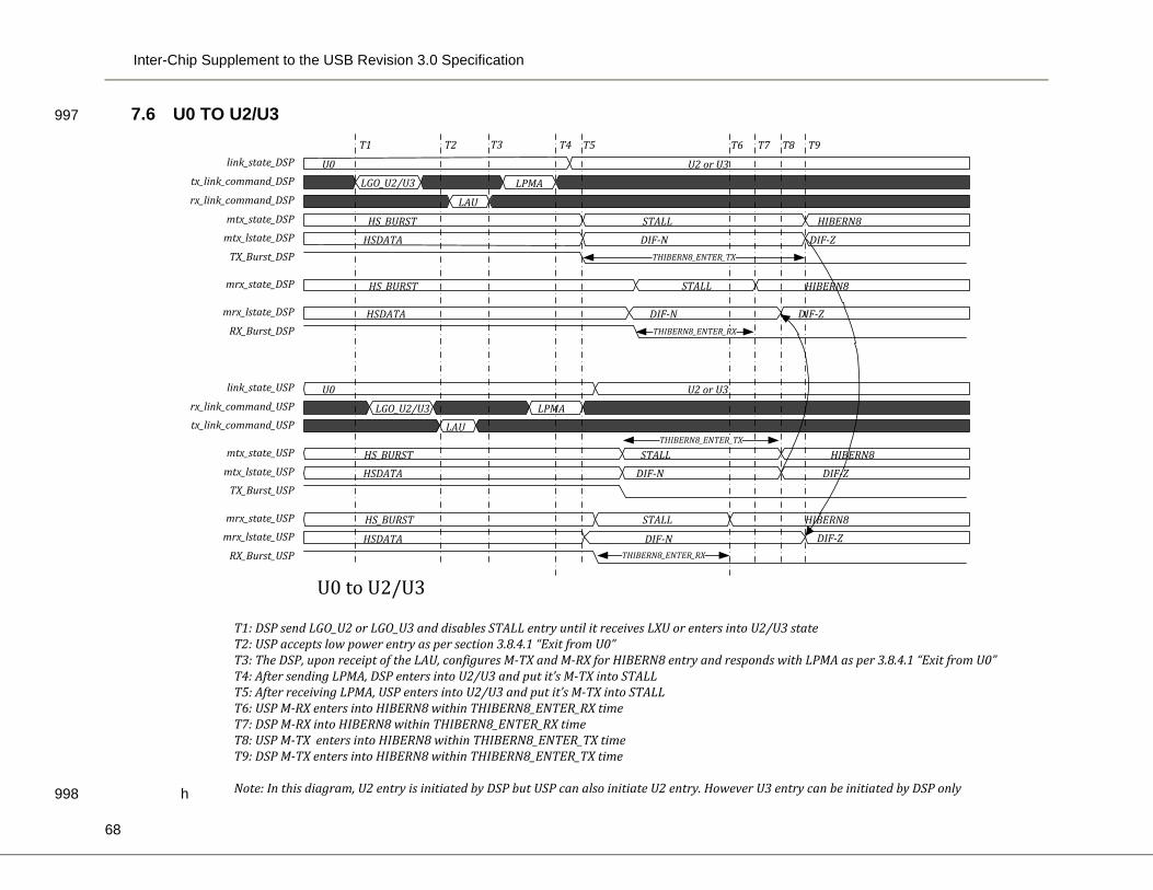
Inter-Chip Supplement to the USB Revision 3.0 Specification
68
7.6 U0 TO U2/U3 997
h 998
HSDATA DIF-N DIF-Z
HS_BURST STALL HIBERN8
HSDATA DIF-N DIF-Z
U0 U2 or U3
HS_BURST STALL HIBERN8
U0 to U2/U3
LGO_U2/U3 LPMA
LAU
HSDATA DIF-N DIF-ZHS_BURST STALL HIBERN8
HSDATA DIF-N DIF-Z
U0 U2 or U3
HS_BURST STALL HIBERN8
LGO_U2/U3 LPMA
LAU
T1: DSP send LGO_U2 or LGO_U3 and disables STALL entry until it receives LXU or enters into U2/U3 stateT2: USP accepts low power entry as per section 3.8.4.1 “Exit from U0”T3: The DSP, upon receipt of the LAU, configures M-TX and M-RX for HIBERN8 entry and responds with LPMA as per 3.8.4.1 “Exit from U0”T4: After sending LPMA, DSP enters into U2/U3 and put it’s M-TX into STALLT5: After receiving LPMA, USP enters into U2/U3 and put it’s M-TX into STALLT6: USP M-RX enters into HIBERN8 within THIBERN8_ENTER_RX timeT7: DSP M-RX into HIBERN8 within THIBERN8_ENTER_RX timeT8: USP M-TX enters into HIBERN8 within THIBERN8_ENTER_TX timeT9: DSP M-TX enters into HIBERN8 within THIBERN8_ENTER_TX time
Note: In this diagram, U2 entry is initiated by DSP but USP can also initiate U2 entry. However U3 entry can be initiated by DSP only
link_state_DSP
tx_link_command_DSP
rx_link_command_DSP
mtx_state_DSP
mtx_lstate_DSP
TX_Burst_DSP
mrx_state_DSP
mrx_lstate_DSP
RX_Burst_DSP
link_state_USP
rx_link_command_USP
tx_link_command_USP
mtx_state_USP
mtx_lstate_USP
TX_Burst_USP
mrx_state_USP
mrx_lstate_USP
RX_Burst_USP
T1 T2 T3 T4 T5 T6 T7 T8
THIBERN8_ENTER_RX
THIBERN8_ENTER_TX
THIBERN8_ENTER_TX
THIBERN8_ENTER_RX
T9
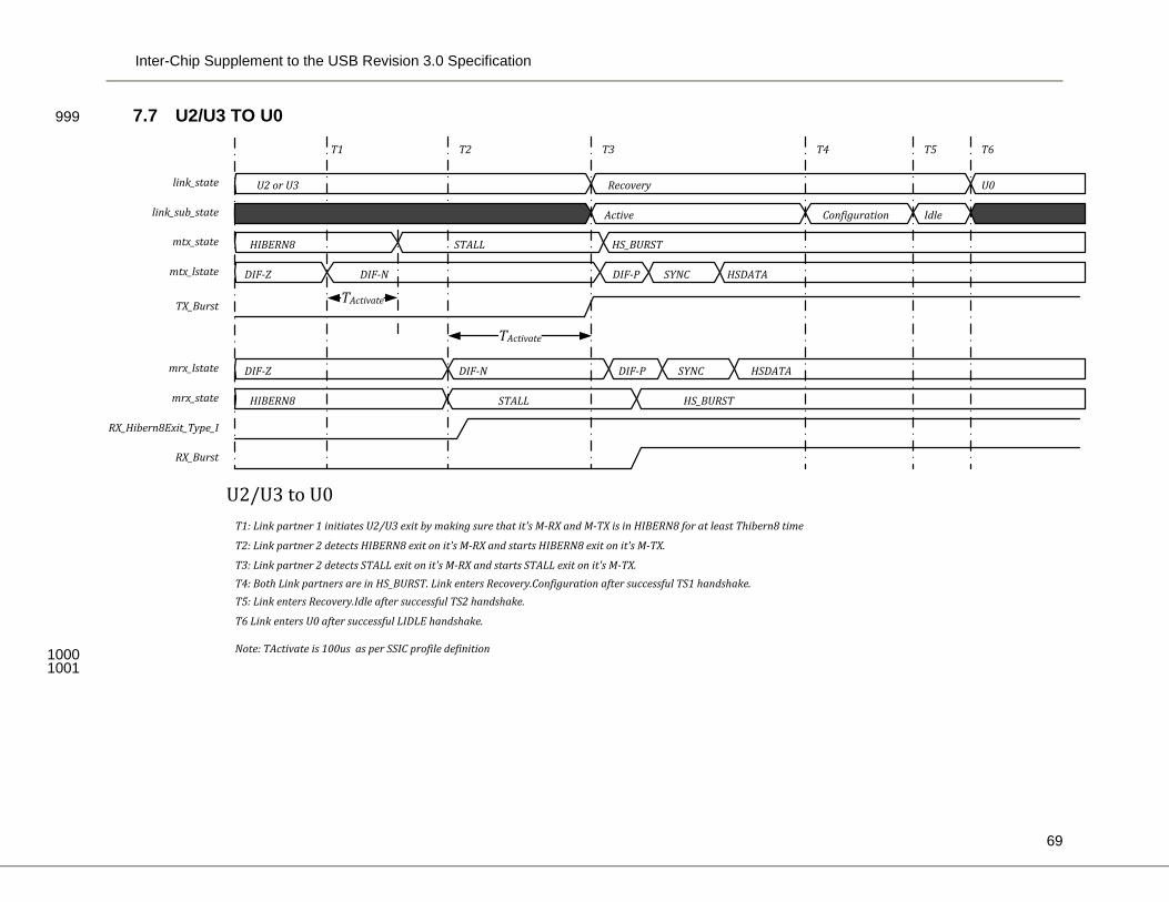
Inter-Chip Supplement to the USB Revision 3.0 Specification
69
7.7 U2/U3 TO U0 999
1000 1001
T1 T2 T3 T4 T5 T6
DIF-Z DIF-N DIF-P SYNC HSDATA
HIBERN8 STALL HS_BURST
DIF-Z DIF-N DIF-P SYNC HSDATA
Active Configuration Idle
U2 or U3 Recovery U0
HIBERN8 STALL HS_BURST
U2/U3 to U0T1: Link partner 1 initiates U2/U3 exit by making sure that it's M-RX and M-TX is in HIBERN8 for at least Thibern8 time
T2: Link partner 2 detects HIBERN8 exit on it's M-RX and starts HIBERN8 exit on it's M-TX.
T3: Link partner 2 detects STALL exit on it's M-RX and starts STALL exit on it's M-TX. T4: Both Link partners are in HS_BURST. Link enters Recovery.Configuration after successful TS1 handshake.T5: Link enters Recovery.Idle after successful TS2 handshake.
T6 Link enters U0 after successful LIDLE handshake.
Note: TActivate is 100us as per SSIC profile definition
link_state
link_sub_state
mtx_state
mtx_lstate
TX_Burst
mrx_lstate
mrx_state
RX_Hibern8Exit_Type_I
RX_Burst
TActivate
TActivate
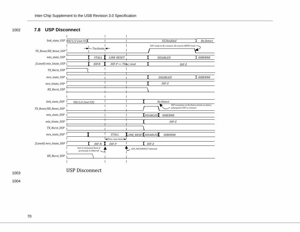
Inter-Chip Supplement to the USB Revision 3.0 Specification
70
7.8 USP Disconnect 1002
1003
1004
link_state_USP
TX_Reset/RX_Reset_USP
mtx_state_USP
(Lane0) mtx_lstate_USP
TX_Burst_USP
mrx_state_USP
mrx_lstate_USP
RX_Burst_USP
link_state_DSP
TX_Reset/RX_Reset_DSP
mtx_state_DSP
mtx_lstate_DSP
TX_Burst_DSP
mrx_state_DSP
(Lane0) mrx_lstate_DSP
RX_Burst_DSP
DIF-P >= Tline_reset
LINE- RESET DISABLED
DIF-Z
HIBERN8
SS.Disabled
DISABLED
DIF-Z
HIBERN8
U0/1/2 (not U3) Rx.Detect
DISABLED HIBERN8
DSP transition to Rx.Detect.Active to detect subsequent USP re-connect
DISABLED
DIF-Z
HIBERN8
USP ready to Re-connect, De-asserts MPHY reset
Rx.Detect
STALL
DIF-N
>= Tactivate
DIF-ZUSP_DISCONNECT detected
DIF-NExit to Activated State if
previously in Hibern8
LINE_RESET
U0/1/2 (not U3)
STALL
DIF-P
USP Disconnect
Tline-reset-detect
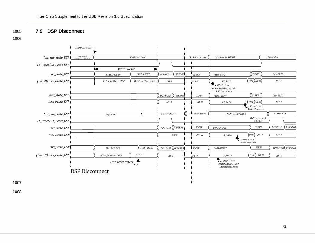
Inter-Chip Supplement to the USB Revision 3.0 Specification
71
7.9 DSP Disconnect 1005
1006
1007
1008
DSP Disconnect
link_sub_state_DSP
TX_Reset/RX_Reset_DSP
mtx_state_DSP
(Lane0) mtx_lstate_DSP
mrx_state_DSP
mrx_lstate_DSP
link_sub_state_USP
TX_Reset/RX_Reset_USP
mtx_state_USP
mtx_lstate_USP
mrx_state_USP
(Lane 0) mrx_lstate_USP
DIF-P >= Tline_reset
LINE- RESET SLEEP
DIF-N
PWM-BURST
Rx.Detect.Active
Rx.Detect.LSMODE SS.Disabled
DSP Disconnect detected
DSP Disconnect
Rx.Detect.LSMODE
STALL/SLEEP
DIF-N for tResetDIFN
DISABLED
DIF-Z
Any states except SS.Disabled
RRAP Write0x400 bit[0]=1, signals
DSP Disconnect
SS.Disabled
Valid RRAP Write Response
DIF- Z
Rx.Detect.Reset
DISABLED HIBERN8
DIF-Z
Valid RRAP Write Response
HIBERN8DISABLED
HIBERN8DISABLED
DIF-P
LINE-RESET SLEEP
DIF- N
STALL/SLEEP DISABLED HIBERN8
DIF-Z
Line-reset-detect
SLEEP
DIF- N
DISABLED HIBERN8
DIF-Z
Any states Rx.Detect.Reset
DIF-NDIF-Z
Rx.Detect.Active
DIF-Z
DIF-N for tResetDIFN
SLEEPDISABLED HIBERN8
RRAP Write0x400 bit[0]=1, DSP
Disconnect detect
Warm ResetSLEEP
TOB DIF-NLS_DATA
PWM-BURST DISABLEDSLEEP
DIF-ZTOB DIF-NLS_DATA
PWM-BURST SLEEP
TOBLS_DATA DIF-N
PWM-BURST SLEEP
TOBLS_DATA DIF-N
Inter-Chip Supplement to the USB Revision 3.0 Specification
72
1009
1010 THIS PAGE IS INTENTIONALLY BLANK TO INDICATE THE END OF THE SUPPLEMENT. 1011