Embed Size (px)
Citation preview

Synthetic Metals, 28 (1989) C715 C721 C715
I~ACE ~ OF C~GANIC S ~ I ~ ~(]NED WITH METAL ~ ~ C
S ~ 4 I ~ .
Mun-Soo Yun, Chang-Su Huh
Korea Electrotechnology Research Institute
Sungju-dong 28-1, Changwon-City, Gyeongnam, Korea
Abstract
We have studied on the junction characteristics of organic semiconductor-metal
and organic semiconductor - inorganic semiconductor devices. Organic semiconduc-
tor was electro-polymerized on metal electrode by constant current method. Con-
sidering the formation of oxide layer at the interface in manufacturing process
and high resistance of organic semiconductor, we can deduce them as a MIS structure.
Usually, it was known that organic semiconductor have rectifying contact with low
workfunction metal and o~mic contact with high workfunction metal. But by our
experimental results, junction characteristics depend on metal oxide layer rather
than workfunction of metals. This oxide layer largely depends on manufacturing
process of devices. So we studied the effect of an electro-polymerization condi-
tion, film thickness, and doping density in junction characteristics. Also we
investigated the solar energy conversion characteristics of these devices. Photon
have to be reached near the depletion region to increase the conversion efficiency.
We studied on the transparent inorganic semiconductor like CdS as a window material
and interface phenomena.
Introduction
A study on the conducting polymer have been continued for a decade from the
pratical and theoretical aspects. But the conducting polymers applicable to prac-
tical device were restricted to a few kinds, because most of them are sensitive to
air. One of them, PPy is c(mparatively stable in air and easy to make thin ~iha
by electrochemical .ool~aerization. So its appl~catioq sbldy have received tnuch
attention from the pratical point of view due to their unique electric and elec-
tronic properties which can be changed by doping process. In many application
0379-6779/89/$3.50 © Elsevier Sequoia/Printed in The Netherlands

C716
aspects, using it as a semiconductor device material is bright due to simplicity of
manufacturing process and large size as ccmpared with other inorganic semiconduc-
tors. On the other hand, organic thin film diode and solar cell are most commer-
cially promising application field for deposited semiconducting film by electro-
chemical method. Junction characteristics of organic-inorganic and metal -organic
semiconducter were studied to investigate the effect of insulating layer at the
interface. Also contact resistance problem was studied with changing the process
of fabrication. Specimen was annealed or metal layer was attached by mechanically
to make the oxide layer at the interface. Also PPy could be used as a solar cell
junction material. In some case charateristics of PPy is similar with inorganic
semiconductor except the kinds of carrier and density of state, so efficiency of
its own junction solar cell is worse than that of schottky or heterojunction with
inorganic semiconductor[l]. We tried to make the junction of inorganic semicon-
ducter with PPy. So we studied CdS properties. We investigated the V-I charac-
teristics as a n~thod to appraise device properties.
Experiment
Polypyrrole was prepared by the electrochemical oxidation. The reaction
solvent was acetonitrile and electrolyte was liti~perchlorate. Before the poly-
merization, pure nitrogen bubbled into it for 30rain. in order to remove dissolved
oxgen. Working electrode was 2X3 cm2 gold film which was vacu~ evaporated on
glass or polymer film substrate.
Also (n)Si wafer was used to make heterojunction. Features of samples were
shown in Fig. i. Weused plati~ plate 2X3 cm 2 as a counter electrode. In order
to control the potential of the working electrode, a saturated calomel electrode
was used as a reference electrode. The total amount of charge passed through the
cell was measured by electrometer (Kethly 602) which has integral calculable abi-
lity. The film deposited on the gold electrode was rinsed with large amount of
methylalcohol and dried in air by hair dryer. Undoping treatment was carried out
by discharge with lead. Also we annealed this sample at 80 - ii0 °C for a few
hours. Indi~ was evaporated under 10-5-106 Torr in area of 0.25 ~2 and Ag paste
was used to decrease the series resistance . V-I characteristics was investigated
with electrometer.
Results and Discussion
We conclude the polypyrrole as a p -type semiconducter by many results. The-
oretically, metals with high work function formed an ohmic contact to this polymer
and low work function metal formed blocking contact. We used A1 as a low workfun-
ction metal which assumed to have blocking contact.

Ag paste
C717
AI203
PPY n-Si
Au electrode
Fig. I -a Structure of ppy/AI heferojunction
Au electrode
SiOz
Ni Ag paste
Fig. I - b Structure of ppy/(n)Si solar cell
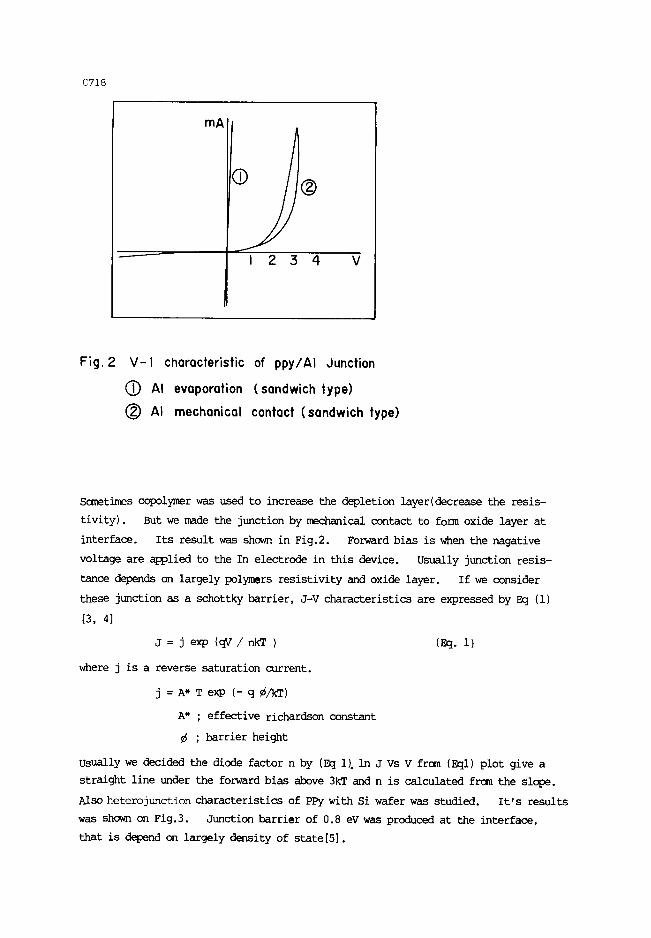
The results of V-I characteristics of A1 /PPy junction were shown in Fig. 2.
Line 1 shows of a ohmic contact and line 2 shows a diode characteristics. PPy was
made by electrochemical method on gold electrode and A1 deposited by vacutml evapora-
tion. Because PPy which have conductivity I0- 101J~/ Cm was not annealed, we
suppose that there is no change on the surface of PPy thin film and tunneling takes
place in the junction, and shows ohmic contact. That result is due to high dopant
density of polymer originally which leads to the narrow depleation region[2].
These narrow depletion region made tunneling coefficient 1 ~d made ohmic contact.
So we treat the polymer with discharge process to control doping density. Conduc-
tivity is proportional to the density of charge carrier, so doping density of poly-
pyrrole depends on largely kinds, and sm~ount of electrolyte. Change of characteri-
stics of device was slight with changing condition of polymerization and undoping
process, so we select a kind of electrolyte, liti~ perchlorate and same concentra-
tion.
Annealing effect on junction characteristics was also studied. Usually poly-
pyrrole is stable in air but by heat treatment the junction characteristics are
changed, which might be due to the oxidation of surface, but could not detect.
C718
mA
.r-"-"
I 2 3 4 V
Fig. 2 V- I characteristic of ppy/AI Junction
0 AI evaporation (sandwich type)
(~) AI mechanical contact (sandwich type)
Sometimes copolymer was used to increase the depletion layer(decrease the resis-
tivity). But we made the junction by mechanical contact to form oxide layer at
interface. Its result was shown in Fig.2. Forward bias is when the nagative
voltage are applied to the In electrode in this device. Usually junction resis-
tance depends on largely polymers resistivity and oxide layer. If we consider
these junction as a schottky barrier, J-V characteristics are expressed by Eq (i)
[3, 4]
J = j exp (qV / nkT ) (Eq. i)
where j is a reverse saturation current.
j = A* T exp (- q 6/kT)
A* ; effective richardson constant
; barrier height
usually we decided the diode factor n by (Eq i). in J Vs V from (Eql) plot give a
straight line under the forward bias above 3kT and n is calculated from the slope.
Also heterojunction characteristics of PPy with Si wafer was studied. It's results
was shown on Fig.3. Junction barrier of 0.8 eV was produced at the interface,
that is depend on largely density of state[5].

C719
mA
2 ®® I 2 3 4 V
Fig. 3 V - I chQrocteristics of (n)Si/ppy Junction (Vot. sup 0.5V/sec)
~) (n)Si/ppy/Au ~ (n)Si/ppy/Au M M M
The discrepancy of 1 and 2 in Fig.3 is due to Au attaching method which were
evaporated or mechanical attach. Forward voltage drop is large ctmparing the
commercial diode. It is due to contact resistance of electrode and space charge
limiting. Basically organic polymer have wide band gap energy and narrow valence
band and conduction band, So carrier was very limited in room te~perautre. Then
mostly carrier of organic device are from space charge injection from contact metal.
So due to its internal and external resistance, forward voltage drop is larger
than that of inorganic semiconducter devices. Usually when we make the solar cell,
p type semiconductor was selected as a photon absorber. Because electron produced
in p type region has faster mobility than that of hole, so probability to overcome
the junction barrier is higher than that of hole by diffusion and drift field. If
photon energy hv is higher than workfunction of absorber, electron was produced and
drift to the junction by diffusion. While traveling the bulk of p type, a part
of electron was trapped at defect or recombinationed with hole. The other overcome
the junction barrier by drift field. At this moment insulating layer which is
located on metal surface effect on the tunneling coefficient.
Photoconductivity of PPy was studied to use it as a photon absorber, but its
response was very crude ctmpare to inorganic semiconductors[6]. So it was used

C720
mA
|
I 2 5 4 5V
Fig. 4 V - I characteristics of (n)Si/ppy Junction
(Vot. sup 4V/sec)
as a junction material to make potential barrier with inorganic semiconductor
which could be solar energy absorber. Firstly V-I characteristics of ppy / Si
was studied at dark and its result was shown in Fig. 4. Hysteresis loop was
produced when we change applied bias voltage and this result are studied contini-
ously. Because PPy was tried as a window material, it has to be very thin.
But there are alway high possibility of puncture, so junction was short. When
we make the film very thick to eliminate puncture, then all optical energy was
absorbed at the surface and efficiency could not be measured. By the way when
we use CdS as a window material, hazardous problem to make good quality CdS thin
film is exist. Though it need heat treatment, this process change the property of
PPy. So we just evaporated Cc]S on PPy without annealing. When we investigated
the V-I characteristic of it in light, voltage is very low, but current is higher
compared to the other persons results which had short current 3uA[7]. We attained
short current 12uA, still we studied to increase the voltage. This SIS or MIS
type solar cell has smaller Io and higher Vo than those of heterojunction or homo-
junction solar cell. Theoretical analysis about insulating layer was studied by
J.Schewchun and A.K.Ghosh, but still was not explained clearly. Usually insula-
ting layer thickness is 10- 20 A in MIS structure. It has tunneling coefficient

C721
1 for minority carrier but not for majority carrier, so Io decreased very severely
with increasing insulating layer thickness. MIS and SIS structure was analyzed
by same theory except top layer of SIS has band gap. But in MIS structure,
solar cell have a many problem due to metal layer thickness which have to be very
thin to increase transparency. By the way in SIS structure, CdS has better
transparancy than that of metal, so there are possibility to increase the efficiency
of solar cell. But solar radiation intensity increase, efficiency are decrease due
to space charge limiting current. It is largest problem in practical point of
view in solar cell to solve.
References
1 S. Miyauchi, A. Fueki, Y. Kushihi Synthetic Metals, 18 (1987) 689-692.
2 H. Koezuka, S. Etoh, J. Appl Phys., 54 (5), May, (1983) 2511-2516.
3 S.R. Forrest, M. L. Kaplan, and P. H. Schmidt, J. Appl Phys., 55 (6), 15 March
(1984) 1492-1507 .
4 S.R. Forrest, M. L. Kaplan, and P. H. SclTnidt, J. Appl~Phys., 60 (7) i, oct
(1986) 2406-2418.
5 O. Ingan~s, T. Skotheim, I. Lundstr~m, J. Appl. Phys., 54 (6), June (1983)
3636-3639.
6 F. Granier, G. Horawitz, Synthetic Metals, 18 (1987) 693-698.
7 D.L. Peebles, J. S. Murday, D. C. Weber, J. Milliken, Journal DE Phys.,
Collgque C3, sul~plement au 6 Tome44 Juin. (1983) C3-591-C3-594.