Embed Size (px)
Citation preview
Interfacing User Logic with the Microcontroller Subsystem
Libero SoC Design Flow Tutorial User’s Guide
Interfacing User Logic with the Microcontroller Subsystem
Interfacing User Logic with the Microcontroller Subsystem 2
Table of Contents
Interfacing User Logic with the Microcontroller Subsystem ..................... 3 Introduction ................................................................................................................................ 3 Tutorial Requirements ................................................................................................................ 3 Design Description ..................................................................................................................... 4 Step 1: Creating a New Libero SoC Project .............................................................................. 5 Step 2: Configuring MSS Functional Blocks .............................................................................. 9 Step 3: Creating Design using SmartDesign ........................................................................... 15 Step 4: Modifying User BFM Script for Simulation ................................................................... 30 Step 5: Simulating Design Using BFM Models ........................................................................ 32 Conclusion ............................................................................................................................... 35
List of Changes ............................................................................................ 37
Product Support .......................................................................................... 39 Customer Service ..................................................................................................................... 39 Customer Technical Support Center ........................................................................................ 39 Technical Support .................................................................................................................... 39 Website .................................................................................................................................... 39 Contacting the Customer Technical Support Center ............................................................... 39 ITAR Technical Support ........................................................................................................... 40
Interfacing User Logic with the Microcontroller Subsystem 3
Interfacing User Logic with the Microcontroller Subsystem
Introduction This tutorial shows you how to interface and handle communication between user logic in the field programmable gate array (FPGA) fabric and the SmartFusion®2 microcontroller subsystem (MSS). It also explains the Microsemi Libero® System-on-Chip (SoC) design software tool flow for designing applications for the SmartFusion2 system-on-chip (SoC) FPGA family of devices. A SmartFusion2 SoC FPGA device has two fabric interface controllers (FIC_0 and FIC_1) as a part of the MSS. These FIC blocks provide a means of interfacing from the SmartFusion2 SoC FPGA MSS AHB-Lite (AHBL) bus to user masters or user slaves in the FPGA fabric. Each FIC block performs an AHBL to AHBL or AHBL to APB3 bridging function between the AHB Bus Matrix and AHBL or APB3 bus in the FPGA fabric. Each FIC block provides two bus interfaces between the MSS and FPGA fabric. The first one is mastered by the MSS and has slaves in the FPGA fabric; the second one has a master in the fabric and slaves in the MSS. The bus interfaces to the FPGA fabric can be either 32-bit AHBL or 32-bit APB type. The FIC block provides registered bridging between the MSS AHBL interface and the FPGA fabric AHBL/APB circuitry to run at frequency ratios of 1:1, 2:1, 4:1, 8:1, 16:1, or 32:1. In AHB-Lite configuration, a bypass mode is provided, in which signals to and from the fabric are not registered and hence requires fewer clock cycles to complete each transaction. SmartFusion2 SoC FPGA FIC has six memory regions. You can allocate a memory region to a particular FIC that is either to FIC_0 or FIC_1. Each memory region has a predefined memory map. Refer to the Fabric Interface Controller chapter of the SmartFusion2 ARM Cortex-M3 and Microcontroller Subsystem User’s Guide for more information on FIC blocks. After completing this tutorial you will be familiar with the following: 1. Creating a project for a SmartFusion2 SoC FPGA using the Microsemi Libero SoC toolset 2. Using SmartFusion2 SoC FPGA MSS configurator to configure MSS blocks 3. Configuring MSS clock conditioning circuitry (MSS_CCC) for generating clocks to the MSS blocks 4. Configuring fabric interface controllers (FIC_0 and FIC_1) to interface user logic in the fabric with the
MSS 5. Using on-chip oscillators and fabric CCC (FAB_CCC) for generating system clocks 6. Writing a simple bus functional model (BFM) script for simulating the design 7. Verifying the design by running BFM commands
Tutorial Requirements This tutorial requires the following software installed on your computer: • Microsemi Libero SoC 11.0.
Project Files The project files associated with this tutorial can be download on Microsemi website: www.microsemi.com/soc/download/rsc/?f=SmartFusion2_FIC_Tutorial_DF. The project files include the following: • Source • Solution • A readme file Refer to the provided readme file for more details on the project files and complete directory structure.
Interfacing User Logic with the Microcontroller Subsystem
4 Interfacing User Logic with the Microcontroller Subsystem
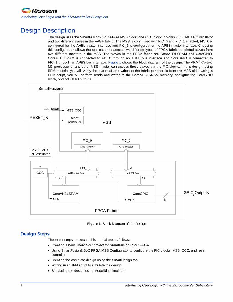
Design Description The design uses the SmartFusion2 SoC FPGA MSS block, one CCC block, on-chip 25/50 MHz RC oscillator and two different slaves in the FPGA fabric. The MSS is configured with FIC_0 and FIC_1 enabled, FIC_0 is configured for the AHBL master interface and FIC_1 is configured for the APB3 master interface. Choosing this configuration allows the application to access two different types of FPGA fabric peripheral slaves from two different masters in the MSS. The slaves in the FPGA fabric are CoreAHBLSRAM and CoreGPIO. CoreAHBLSRAM is connected to FIC_0 through an AHBL bus interface and CoreGPIO is connected to FIC_1 through an APB3 bus interface. Figure 1 shows the block diagram of the design. The ARM® Cortex-M3 processor or any other MSS master can access these slaves via the FIC blocks. In this design, using BFM models, you will verify the bus read and writes to the fabric peripherals from the MSS side. Using a BFM script, you will perform reads and writes to the CoreAHBLSRAM memory, configure the CoreGPIO block, and set GPIO outputs.
MSS
FIC_0 FIC_1
AHB-Lite Bus APB3 Bus
CoreAHBLSRAM CoreGPIO
M0
S5
M
S8
AHB Master APB Master
FPGA Fabric
SmartFusion2
RESET_N
GPIO Outputs
25/50 MHz RC oscillator
MSS_CCC
Reset Controller
CCC
CLK CLK
CLK_BASE
8
Figure 1. Block Diagram of the Design
Design Steps The major steps to execute this tutorial are as follows: • Creating a new Libero SoC project for SmartFusion2 SoC FPGA • Using SmartFusion2 SoC FPGA MSS Configurator to configure the FIC blocks, MSS_CCC, and reset
controller • Creating the complete design using the SmartDesign tool • Writing user BFM script to simulate the design • Simulating the design using ModelSim simulator
Step 1: Creating a New Libero SoC Project
Interfacing User Logic with the Microcontroller Subsystem 5
Step 1: Creating a New Libero SoC Project 1. Open Libero SoC design software (Start > Programs > Microsemi Libero SoC 11.0 > Libero SoC
11.0) or click the Libero SoC shortcut available on your desktop. The version number of the Libero SoC design software depends on the version that is installed on your PC. You can use either v11.0 or latest.
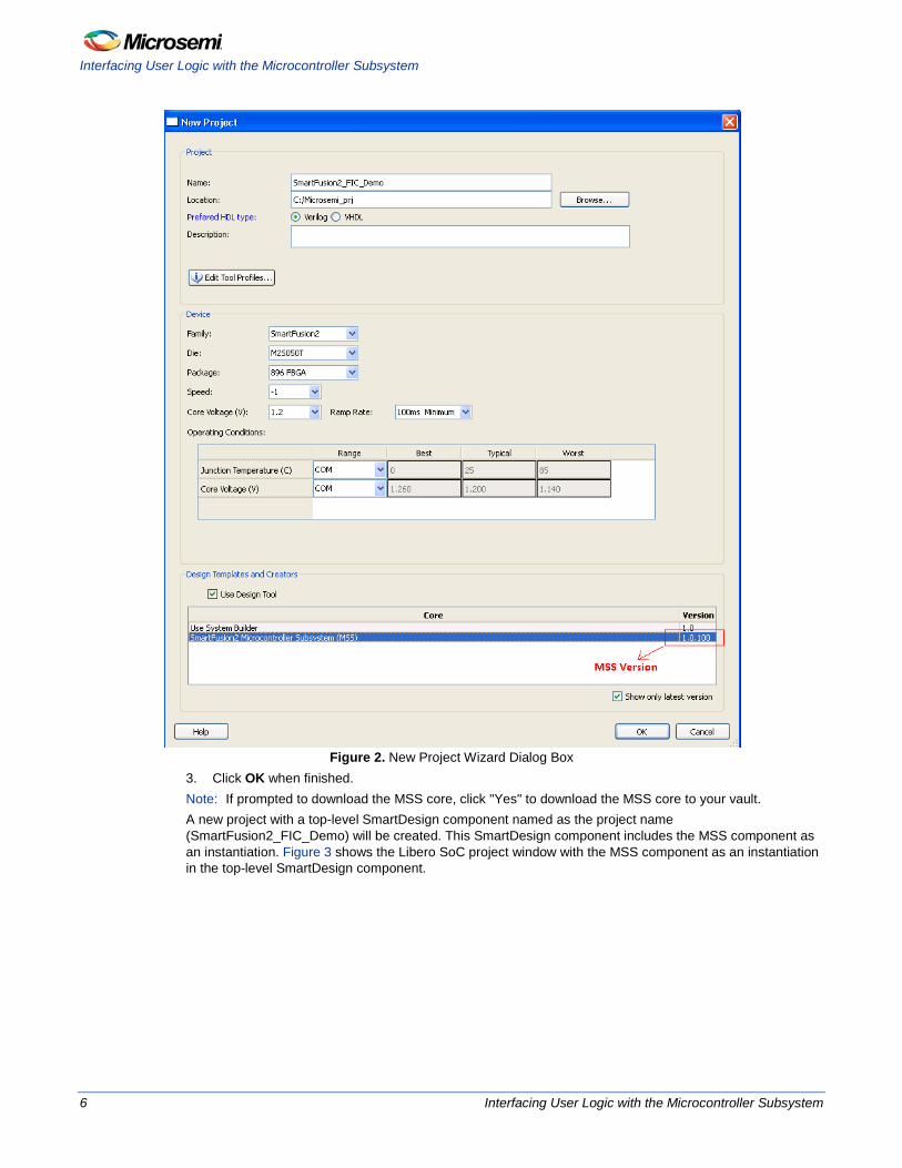
2. Select New Project from the Project menu. Enter the information shown below in the New Project wizard dialog box. • Project Name: SmartFusion2_FIC_Demo • Location: C:/Microsemi_prj • Preferred HDL type: Verilog • Family: SmartFusion2 • Die: M2S050T • Package: 896 FBGA • Speed: -1 • Die Voltage: 1.2 • Operating Conditions: COM • Design Templates and Creators: Select Use Design Tool and select SmartFusion2 Microcontroller
Subsystem (MSS) under core section. Note: This tutorial uses Verilog as the preferred HDL type. You can select VHDL as the preferred HDL
type and continue with the tutorial. This tutorial uses MSS version 1.0.100. It is recommended to use the latest version of the MSS for your designs.
Interfacing User Logic with the Microcontroller Subsystem
6 Interfacing User Logic with the Microcontroller Subsystem
Figure 2. New Project Wizard Dialog Box
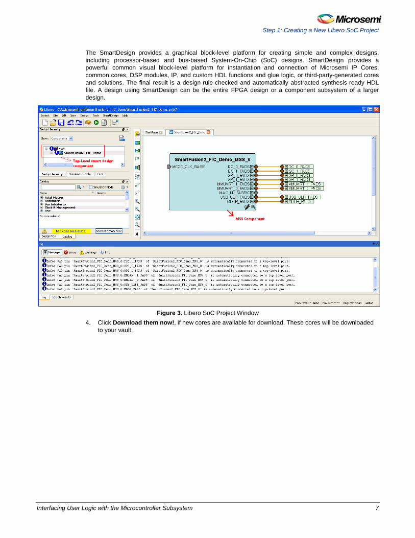
3. Click OK when finished. Note: If prompted to download the MSS core, click "Yes" to download the MSS core to your vault. A new project with a top-level SmartDesign component named as the project name (SmartFusion2_FIC_Demo) will be created. This SmartDesign component includes the MSS component as an instantiation. Figure 3 shows the Libero SoC project window with the MSS component as an instantiation in the top-level SmartDesign component.
Step 1: Creating a New Libero SoC Project
Interfacing User Logic with the Microcontroller Subsystem 7
The SmartDesign provides a graphical block-level platform for creating simple and complex designs, including processor-based and bus-based System-On-Chip (SoC) designs. SmartDesign provides a powerful common visual block-level platform for instantiation and connection of Microsemi IP Cores, common cores, DSP modules, IP, and custom HDL functions and glue logic, or third-party-generated cores and solutions. The final result is a design-rule-checked and automatically abstracted synthesis-ready HDL file. A design using SmartDesign can be the entire FPGA design or a component subsystem of a larger design.
Figure 3. Libero SoC Project Window
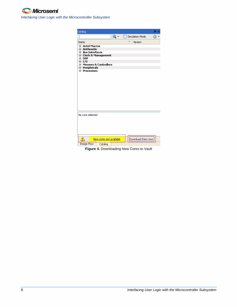
4. Click Download them now!, if new cores are available for download. These cores will be downloaded to your vault.
Interfacing User Logic with the Microcontroller Subsystem
8 Interfacing User Logic with the Microcontroller Subsystem
Figure 4. Downloading New Cores to Vault
Step 2: Configuring MSS Functional Blocks
Interfacing User Logic with the Microcontroller Subsystem 9
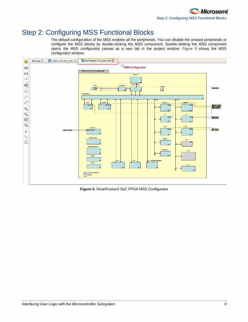
Step 2: Configuring MSS Functional Blocks The default configuration of the MSS enables all the peripherals. You can disable the unused peripherals or configure the MSS blocks by double-clicking the MSS component. Double-clicking the MSS component opens the MSS configurator canvas as a new tab in the project window. Figure 5 shows the MSS configurator window.
Figure 5. SmartFusion2 SoC FPGA MSS Configurator
Interfacing User Logic with the Microcontroller Subsystem
10 Interfacing User Logic with the Microcontroller Subsystem
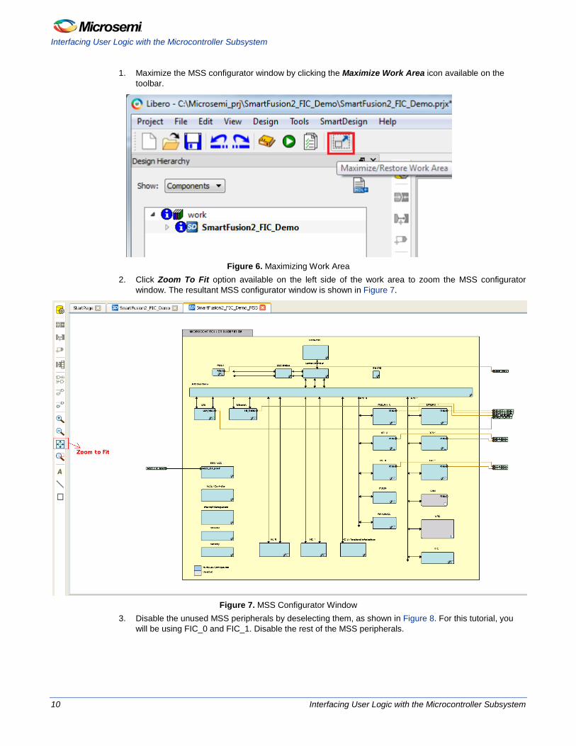
1. Maximize the MSS configurator window by clicking the Maximize Work Area icon available on the toolbar.
Figure 6. Maximizing Work Area
2. Click Zoom To Fit option available on the left side of the work area to zoom the MSS configurator window. The resultant MSS configurator window is shown in Figure 7.
Figure 7. MSS Configurator Window
3. Disable the unused MSS peripherals by deselecting them, as shown in Figure 8. For this tutorial, you will be using FIC_0 and FIC_1. Disable the rest of the MSS peripherals.

Step 2: Configuring MSS Functional Blocks
Interfacing User Logic with the Microcontroller Subsystem 11
Figure 8. Disabling Unused Peripherals
4. The resultant MSS configurator window after disabling the unused MSS peripherals is shown in Figure 9.
Figure 9. MSS Configurator with Unused MSS Peripherals Unchecked
5. Configure the FIC_0 block for an AHBL master interface by double-clicking it. A FIC_0 configurator window is displayed. In the FIC_0 configurator, make the following settings and keep the others at the default settings: • Interface Type: AHBLite • Use Master Interface: Enable • FPGA Fabric Address Regions (MSS Master View): Allocate Fabric Region 0, 1, and 2 to FIC_0 and
Fabric Region 3, 4, and 5 to FIC_1. This is the default setting. This configuration allows the MSS Masters to access the fabric slaves at fabric regions 0, 1, and 2 through FIC_0, and fabric regions 3, 4, and 5 via FIC_1.
Interfacing User Logic with the Microcontroller Subsystem
12 Interfacing User Logic with the Microcontroller Subsystem
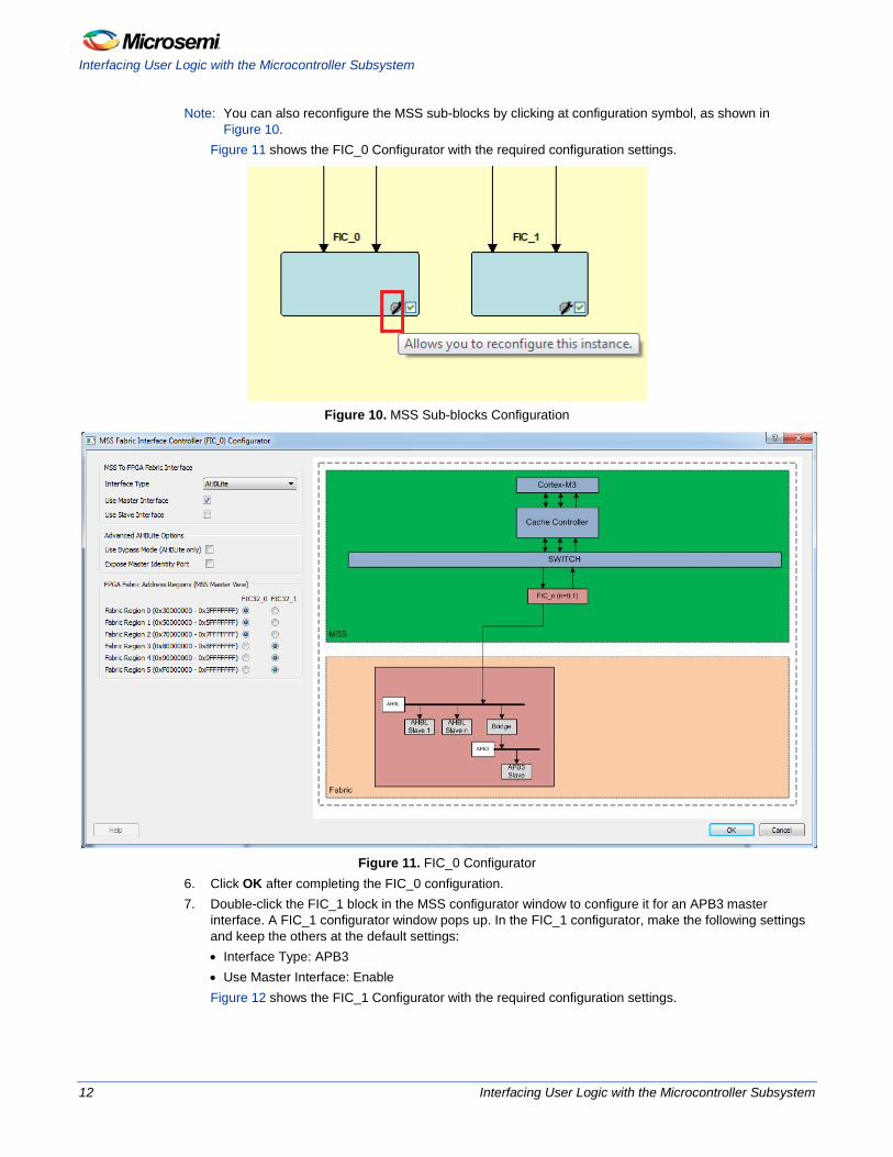
Note: You can also reconfigure the MSS sub-blocks by clicking at configuration symbol, as shown in Figure 10.
Figure 11 shows the FIC_0 Configurator with the required configuration settings.
Figure 10. MSS Sub-blocks Configuration
Figure 11. FIC_0 Configurator
6. Click OK after completing the FIC_0 configuration. 7. Double-click the FIC_1 block in the MSS configurator window to configure it for an APB3 master
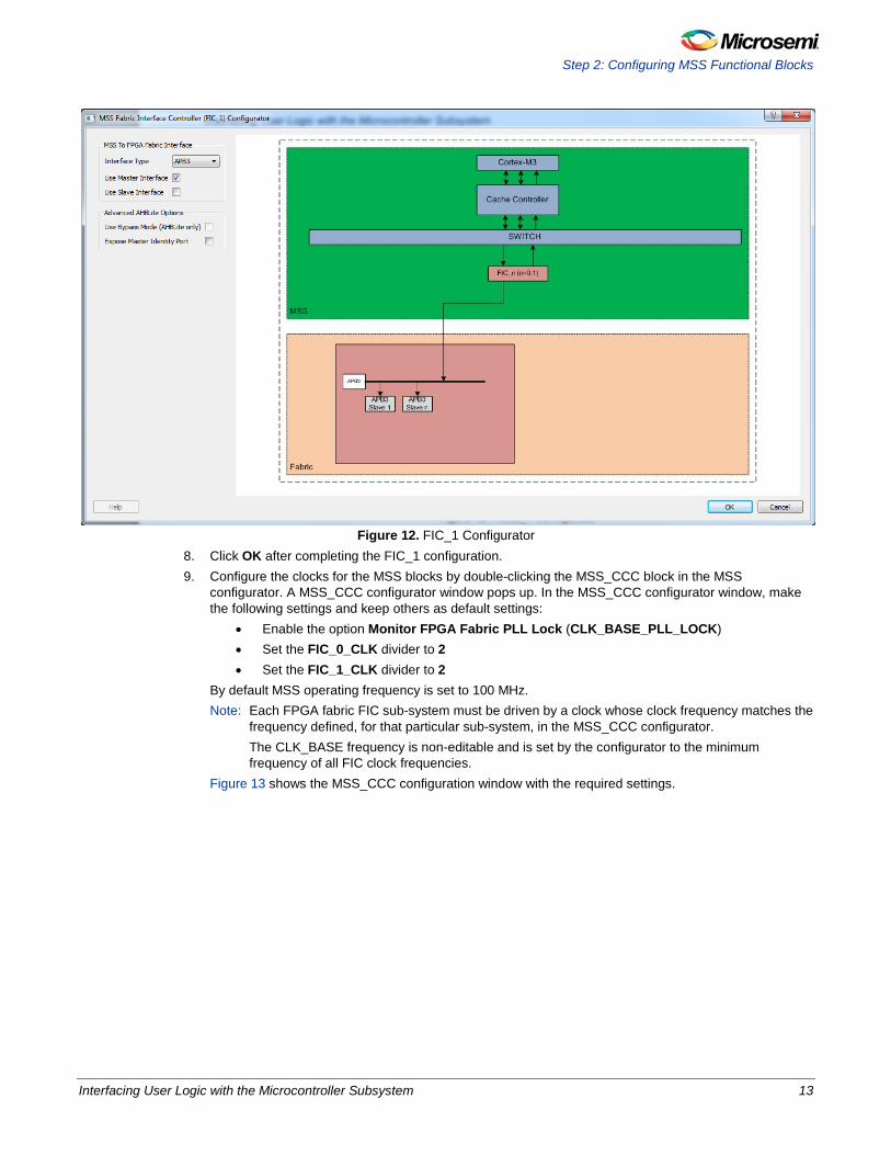
interface. A FIC_1 configurator window pops up. In the FIC_1 configurator, make the following settings and keep the others at the default settings: • Interface Type: APB3 • Use Master Interface: Enable Figure 12 shows the FIC_1 Configurator with the required configuration settings.
Step 2: Configuring MSS Functional Blocks
Interfacing User Logic with the Microcontroller Subsystem 13
Figure 12. FIC_1 Configurator
8. Click OK after completing the FIC_1 configuration. 9. Configure the clocks for the MSS blocks by double-clicking the MSS_CCC block in the MSS
configurator. A MSS_CCC configurator window pops up. In the MSS_CCC configurator window, make the following settings and keep others as default settings:
• Enable the option Monitor FPGA Fabric PLL Lock (CLK_BASE_PLL_LOCK) • Set the FIC_0_CLK divider to 2 • Set the FIC_1_CLK divider to 2
By default MSS operating frequency is set to 100 MHz. Note: Each FPGA fabric FIC sub-system must be driven by a clock whose clock frequency matches the
frequency defined, for that particular sub-system, in the MSS_CCC configurator. The CLK_BASE frequency is non-editable and is set by the configurator to the minimum frequency of all FIC clock frequencies.
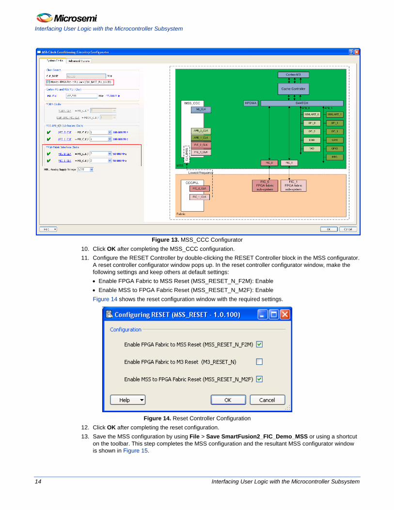
Figure 13 shows the MSS_CCC configuration window with the required settings.
Interfacing User Logic with the Microcontroller Subsystem
14 Interfacing User Logic with the Microcontroller Subsystem
Figure 13. MSS_CCC Configurator
10. Click OK after completing the MSS_CCC configuration. 11. Configure the RESET Controller by double-clicking the RESET Controller block in the MSS configurator.
A reset controller configurator window pops up. In the reset controller configurator window, make the following settings and keep others at default settings: • Enable FPGA Fabric to MSS Reset (MSS_RESET_N_F2M): Enable • Enable MSS to FPGA Fabric Reset (MSS_RESET_N_M2F): Enable Figure 14 shows the reset configuration window with the required settings.
Figure 14. Reset Controller Configuration
12. Click OK after completing the reset configuration. 13. Save the MSS configuration by using File > Save SmartFusion2_FIC_Demo_MSS or using a shortcut
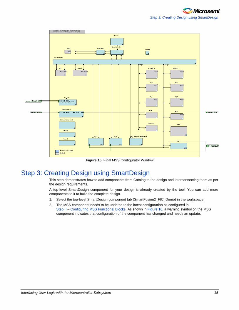
on the toolbar. This step completes the MSS configuration and the resultant MSS configurator window is shown in Figure 15.
Step 3: Creating Design using SmartDesign
Interfacing User Logic with the Microcontroller Subsystem 15
Figure 15. Final MSS Configurator Window
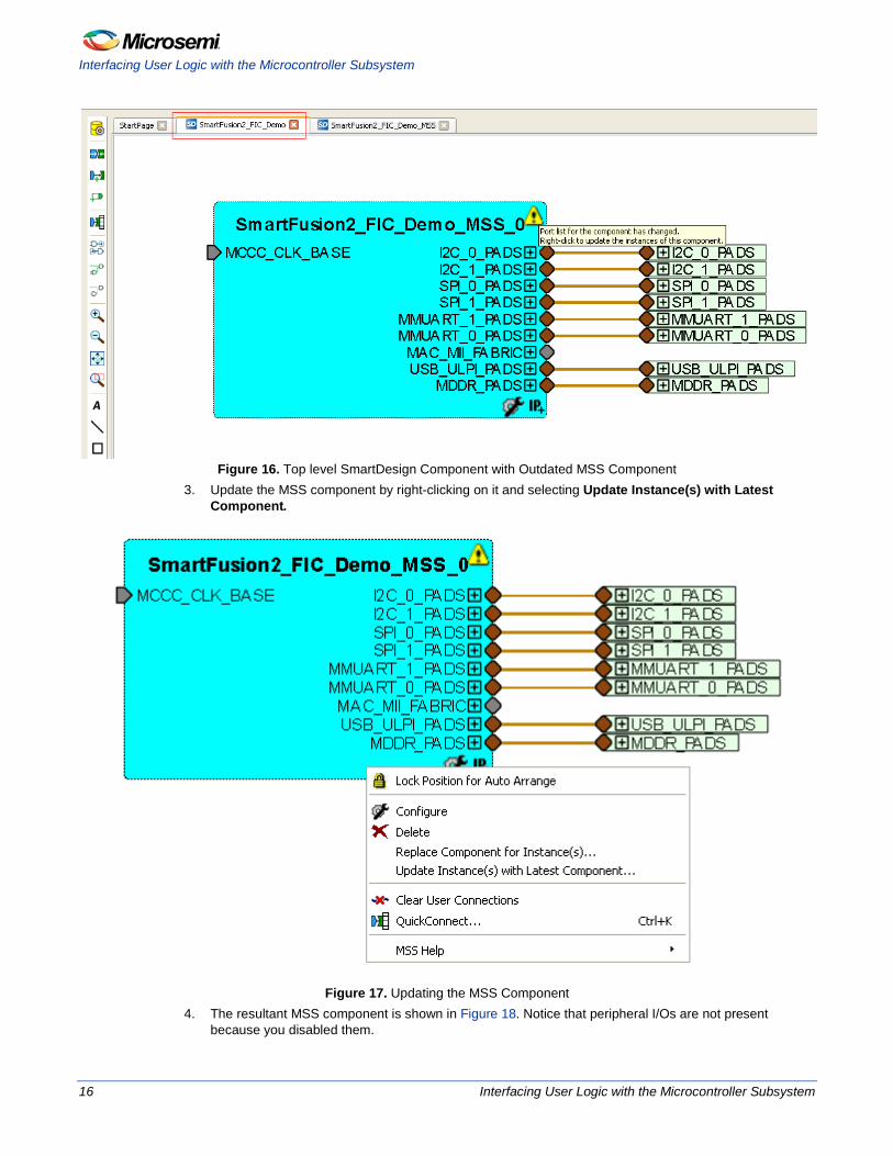
Step 3: Creating Design using SmartDesign This step demonstrates how to add components from Catalog to the design and interconnecting them as per the design requirements. A top-level SmartDesign component for your design is already created by the tool. You can add more components to it to build the complete design. 1. Select the top-level SmartDesign component tab (SmartFusion2_FIC_Demo) in the workspace. 2. The MSS component needs to be updated to the latest configuration as configured in
Step II – Configuring MSS Functional Blocks. As shown in Figure 16, a warning symbol on the MSS component indicates that configuration of the component has changed and needs an update.
Interfacing User Logic with the Microcontroller Subsystem
16 Interfacing User Logic with the Microcontroller Subsystem
Figure 16. Top level SmartDesign Component with Outdated MSS Component
3. Update the MSS component by right-clicking on it and selecting Update Instance(s) with Latest Component.
Figure 17. Updating the MSS Component
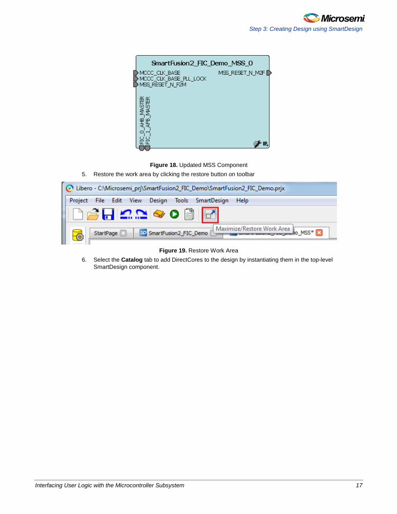
4. The resultant MSS component is shown in Figure 18. Notice that peripheral I/Os are not present because you disabled them.
Step 3: Creating Design using SmartDesign
Interfacing User Logic with the Microcontroller Subsystem 17
Figure 18. Updated MSS Component
5. Restore the work area by clicking the restore button on toolbar
Figure 19. Restore Work Area
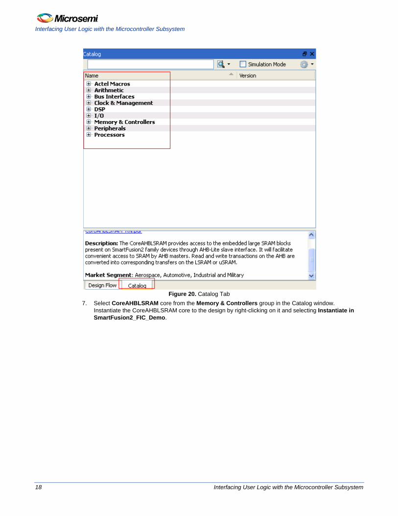
6. Select the Catalog tab to add DirectCores to the design by instantiating them in the top-level SmartDesign component.
Interfacing User Logic with the Microcontroller Subsystem
18 Interfacing User Logic with the Microcontroller Subsystem
Figure 20. Catalog Tab
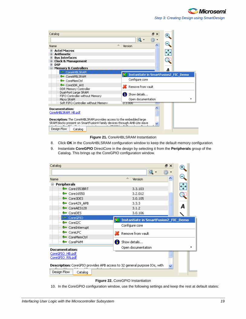
7. Select CoreAHBLSRAM core from the Memory & Controllers group in the Catalog window. Instantiate the CoreAHBLSRAM core to the design by right-clicking on it and selecting Instantiate in SmartFusion2_FIC_Demo.
Step 3: Creating Design using SmartDesign
Interfacing User Logic with the Microcontroller Subsystem 19
Figure 21. CoreAHBLSRAM Instantiation
8. Click OK in the CoreAHBLSRAM configuration window to keep the default memory configuration. 9. Instantiate CoreGPIO DirectCore in the design by selecting it from the Peripherals group of the
Catalog. This brings up the CoreGPIO configuration window.
Figure 22. CoreGPIO Instantiation
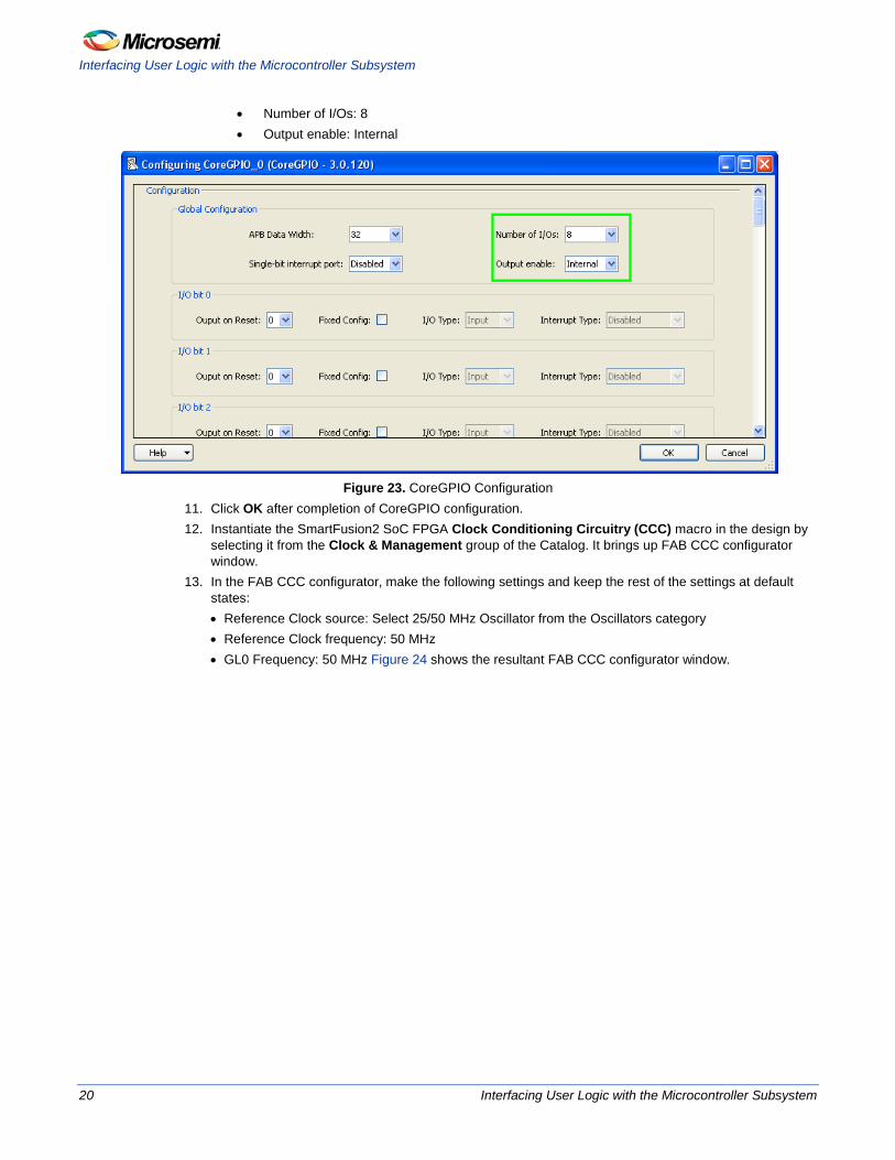
10. In the CoreGPIO configuration window, use the following settings and keep the rest at default states:
Interfacing User Logic with the Microcontroller Subsystem
20 Interfacing User Logic with the Microcontroller Subsystem
• Number of I/Os: 8 • Output enable: Internal
Figure 23. CoreGPIO Configuration
11. Click OK after completion of CoreGPIO configuration. 12. Instantiate the SmartFusion2 SoC FPGA Clock Conditioning Circuitry (CCC) macro in the design by
selecting it from the Clock & Management group of the Catalog. It brings up FAB CCC configurator window.
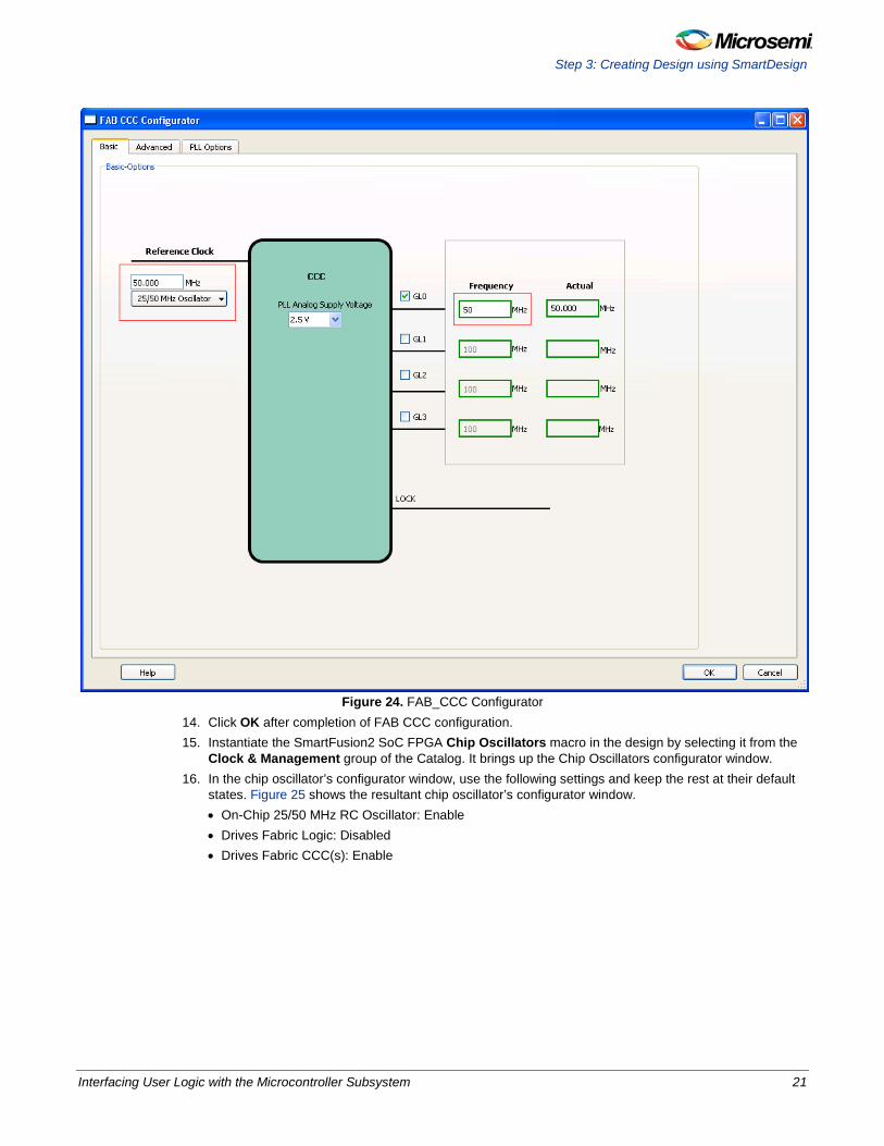
13. In the FAB CCC configurator, make the following settings and keep the rest of the settings at default states: • Reference Clock source: Select 25/50 MHz Oscillator from the Oscillators category • Reference Clock frequency: 50 MHz • GL0 Frequency: 50 MHz Figure 24 shows the resultant FAB CCC configurator window.
Step 3: Creating Design using SmartDesign
Interfacing User Logic with the Microcontroller Subsystem 21
Figure 24. FAB_CCC Configurator
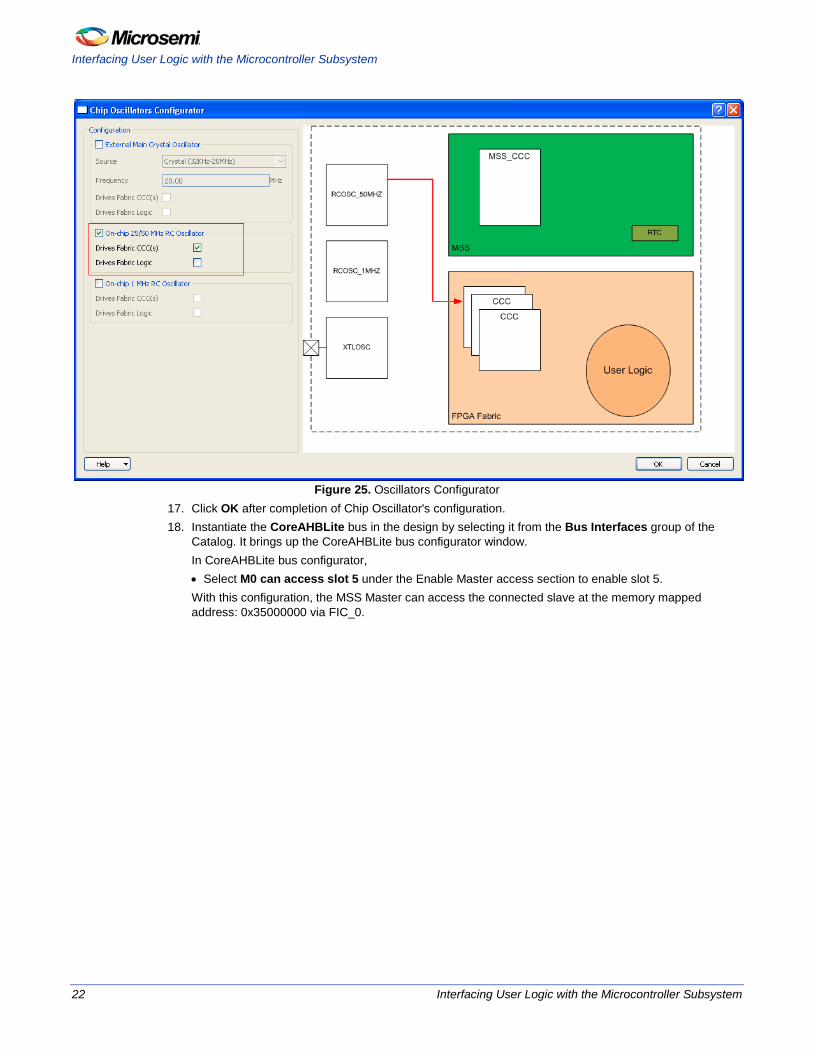
14. Click OK after completion of FAB CCC configuration. 15. Instantiate the SmartFusion2 SoC FPGA Chip Oscillators macro in the design by selecting it from the
Clock & Management group of the Catalog. It brings up the Chip Oscillators configurator window. 16. In the chip oscillator’s configurator window, use the following settings and keep the rest at their default
states. Figure 25 shows the resultant chip oscillator’s configurator window. • On-Chip 25/50 MHz RC Oscillator: Enable • Drives Fabric Logic: Disabled • Drives Fabric CCC(s): Enable
Interfacing User Logic with the Microcontroller Subsystem
22 Interfacing User Logic with the Microcontroller Subsystem
Figure 25. Oscillators Configurator
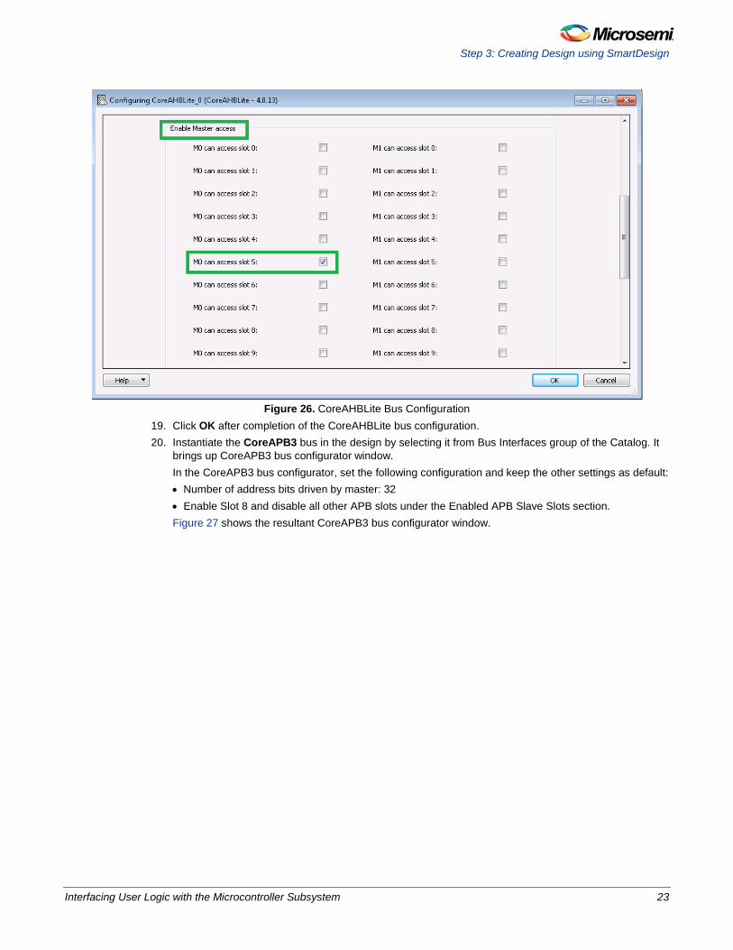
17. Click OK after completion of Chip Oscillator's configuration. 18. Instantiate the CoreAHBLite bus in the design by selecting it from the Bus Interfaces group of the
Catalog. It brings up the CoreAHBLite bus configurator window. In CoreAHBLite bus configurator, • Select M0 can access slot 5 under the Enable Master access section to enable slot 5. With this configuration, the MSS Master can access the connected slave at the memory mapped address: 0x35000000 via FIC_0.
Step 3: Creating Design using SmartDesign
Interfacing User Logic with the Microcontroller Subsystem 23
Figure 26. CoreAHBLite Bus Configuration
19. Click OK after completion of the CoreAHBLite bus configuration. 20. Instantiate the CoreAPB3 bus in the design by selecting it from Bus Interfaces group of the Catalog. It
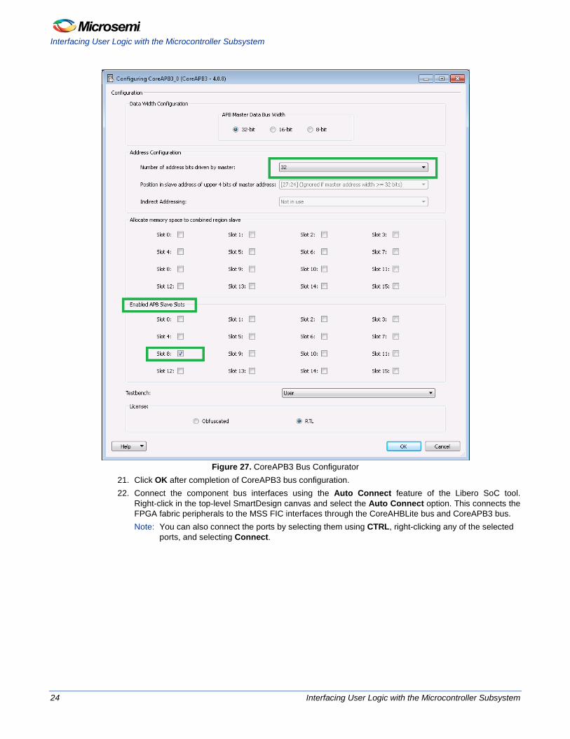
brings up CoreAPB3 bus configurator window. In the CoreAPB3 bus configurator, set the following configuration and keep the other settings as default: • Number of address bits driven by master: 32 • Enable Slot 8 and disable all other APB slots under the Enabled APB Slave Slots section. Figure 27 shows the resultant CoreAPB3 bus configurator window.
Interfacing User Logic with the Microcontroller Subsystem
24 Interfacing User Logic with the Microcontroller Subsystem
Figure 27. CoreAPB3 Bus Configurator
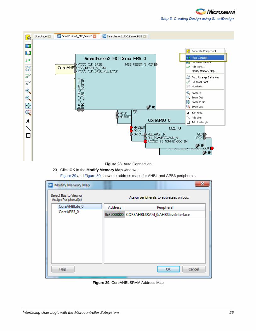
21. Click OK after completion of CoreAPB3 bus configuration. 22. Connect the component bus interfaces using the Auto Connect feature of the Libero SoC tool.
Right-click in the top-level SmartDesign canvas and select the Auto Connect option. This connects the FPGA fabric peripherals to the MSS FIC interfaces through the CoreAHBLite bus and CoreAPB3 bus. Note: You can also connect the ports by selecting them using CTRL, right-clicking any of the selected
ports, and selecting Connect.
Step 3: Creating Design using SmartDesign
Interfacing User Logic with the Microcontroller Subsystem 25
Figure 28. Auto Connection
23. Click OK in the Modify Memory Map window. Figure 29 and Figure 30 show the address maps for AHBL and APB3 peripherals.
Figure 29. CoreAHBLSRAM Address Map
Interfacing User Logic with the Microcontroller Subsystem
26 Interfacing User Logic with the Microcontroller Subsystem
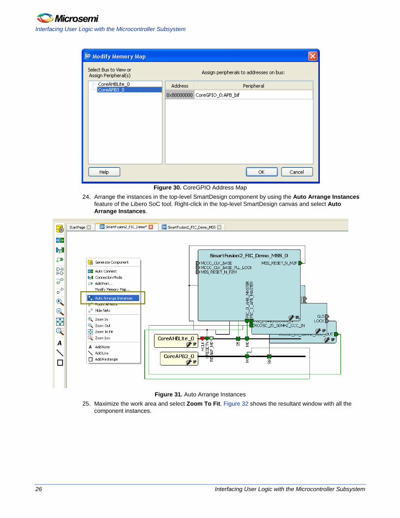
Figure 30. CoreGPIO Address Map
24. Arrange the instances in the top-level SmartDesign component by using the Auto Arrange Instances feature of the Libero SoC tool. Right-click in the top-level SmartDesign canvas and select Auto Arrange Instances.
Figure 31. Auto Arrange Instances
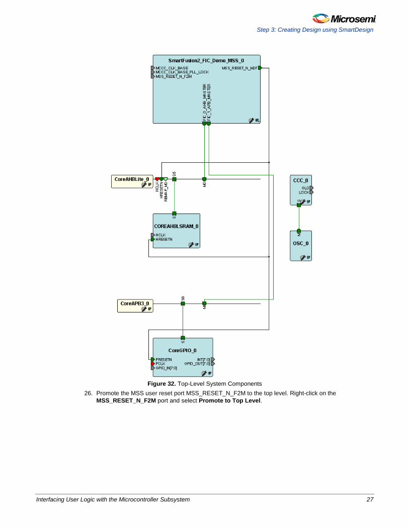
25. Maximize the work area and select Zoom To Fit. Figure 32 shows the resultant window with all the component instances.
Step 3: Creating Design using SmartDesign
Interfacing User Logic with the Microcontroller Subsystem 27
Figure 32. Top-Level System Components
26. Promote the MSS user reset port MSS_RESET_N_F2M to the top level. Right-click on the MSS_RESET_N_F2M port and select Promote to Top Level.
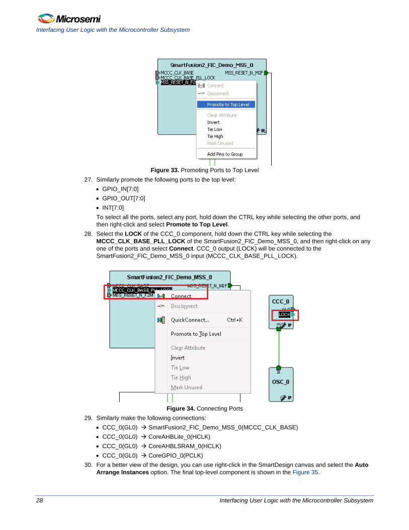
Interfacing User Logic with the Microcontroller Subsystem
28 Interfacing User Logic with the Microcontroller Subsystem
Figure 33. Promoting Ports to Top Level
27. Similarly promote the following ports to the top level: • GPIO_IN[7:0] • GPIO_OUT[7:0] • INT[7:0] To select all the ports, select any port, hold down the CTRL key while selecting the other ports, and then right-click and select Promote to Top Level.
28. Select the LOCK of the CCC_0 component, hold down the CTRL key while selecting the MCCC_CLK_BASE_PLL_LOCK of the SmartFusion2_FIC_Demo_MSS_0, and then right-click on any one of the ports and select Connect. CCC_0 output (LOCK) will be connected to the SmartFusion2_FIC_Demo_MSS_0 input (MCCC_CLK_BASE_PLL_LOCK).
Figure 34. Connecting Ports
29. Similarly make the following connections: • CCC_0(GL0) SmartFusion2_FIC_Demo_MSS_0(MCCC_CLK_BASE) • CCC_0(GL0) CoreAHBLite_0(HCLK) • CCC_0(GL0) CoreAHBLSRAM_0(HCLK) • CCC_0(GL0) CoreGPIO_0(PCLK)
30. For a better view of the design, you can use right-click in the SmartDesign canvas and select the Auto Arrange Instances option. The final top-level component is shown in the Figure 35.

Step 3: Creating Design using SmartDesign
Interfacing User Logic with the Microcontroller Subsystem 29
Figure 35. Final Top Level Component
31. Restore the work area by clicking the Restore on the toolbar. 32. Save the project by clicking Project > Save SmartFision2_FIC_demo. 33. Generate the top-level SmartDesign component by clicking the Generate button, as shown in the
Figure 36.
Figure 36. Generate the Top Level SmartDesign Component
Interfacing User Logic with the Microcontroller Subsystem
30 Interfacing User Logic with the Microcontroller Subsystem
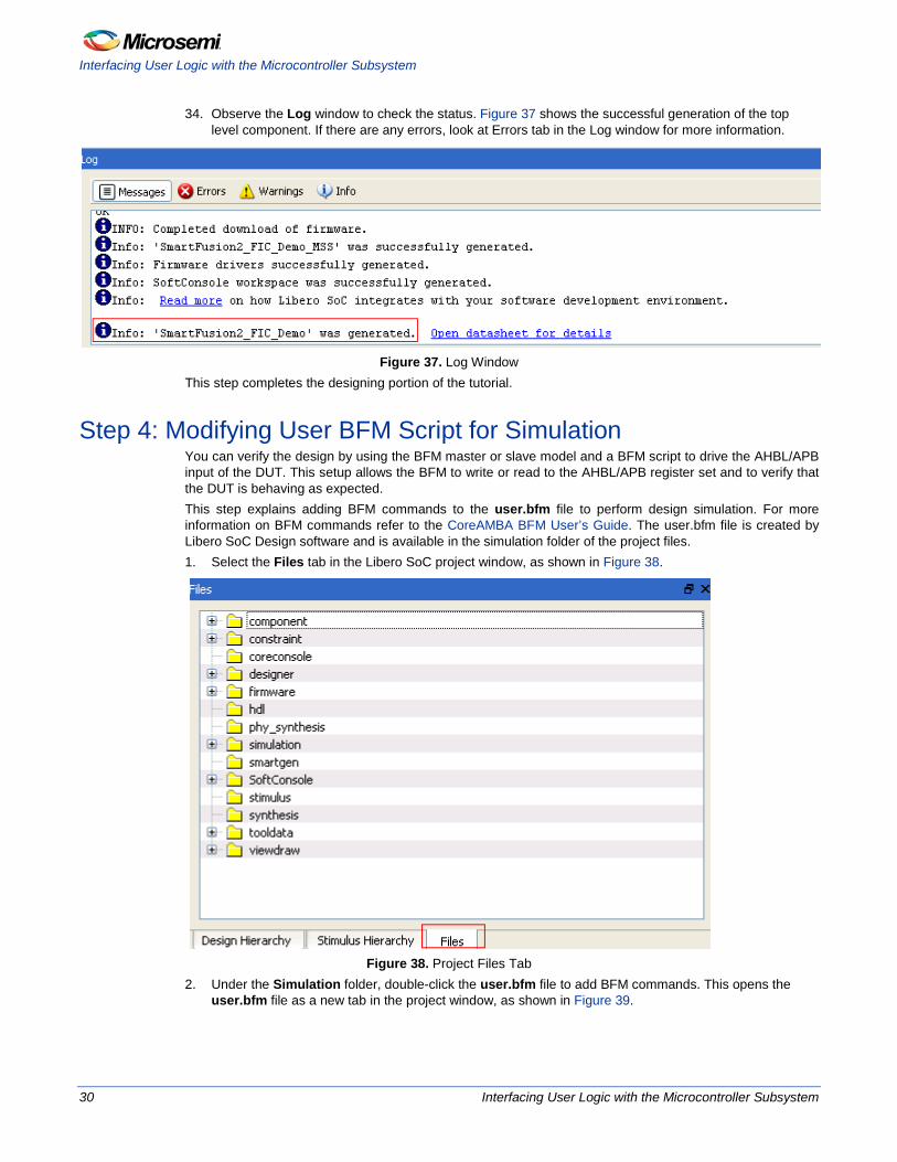
34. Observe the Log window to check the status. Figure 37 shows the successful generation of the top level component. If there are any errors, look at Errors tab in the Log window for more information.
Figure 37. Log Window
This step completes the designing portion of the tutorial.
Step 4: Modifying User BFM Script for Simulation You can verify the design by using the BFM master or slave model and a BFM script to drive the AHBL/APB input of the DUT. This setup allows the BFM to write or read to the AHBL/APB register set and to verify that the DUT is behaving as expected. This step explains adding BFM commands to the user.bfm file to perform design simulation. For more information on BFM commands refer to the CoreAMBA BFM User’s Guide. The user.bfm file is created by Libero SoC Design software and is available in the simulation folder of the project files. 1. Select the Files tab in the Libero SoC project window, as shown in Figure 38.
Figure 38. Project Files Tab
2. Under the Simulation folder, double-click the user.bfm file to add BFM commands. This opens the user.bfm file as a new tab in the project window, as shown in Figure 39.
Step 4: Modifying User BFM Script for Simulation
Interfacing User Logic with the Microcontroller Subsystem 31
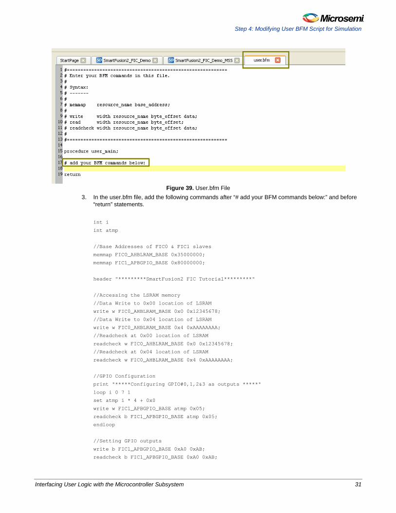
Figure 39. User.bfm File
3. In the user.bfm file, add the following commands after “# add your BFM commands below:” and before “return” statements.
int i
int atmp
//Base Addresses of FIC0 & FIC1 slaves
memmap FIC0_AHBLRAM_BASE 0x35000000;
memmap FIC1_APBGPIO_BASE 0x80000000;
header "*********SmartFusion2 FIC Tutorial*********"
//Accessing the LSRAM memory
//Data Write to 0x00 location of LSRAM
write w FIC0_AHBLRAM_BASE 0x0 0x12345678;
//Data Write to 0x04 location of LSRAM
write w FIC0_AHBLRAM_BASE 0x4 0xAAAAAAAA;
//Readcheck at 0x00 location of LSRAM
readcheck w FIC0_AHBLRAM_BASE 0x0 0x12345678;
//Readcheck at 0x04 location of LSRAM
readcheck w FIC0_AHBLRAM_BASE 0x4 0xAAAAAAAA;
//GPIO Configuration
print "*****Configuring GPIO#0,1,2&3 as outputs *****"
loop i 0 7 1
set atmp i * 4 + 0x0
write w FIC1_APBGPIO_BASE atmp 0x05;
readcheck b FIC1_APBGPIO_BASE atmp 0x05;
endloop
//Setting GPIO outputs
write b FIC1_APBGPIO_BASE 0xA0 0xAB;
readcheck b FIC1_APBGPIO_BASE 0xA0 0xAB;
Interfacing User Logic with the Microcontroller Subsystem
32 Interfacing User Logic with the Microcontroller Subsystem
4. Comment the below lines in user.bfm file by keeping '#' at the starting of these lines: include "subsystem.bfm"
call subsystem_init;
5. Save the user.bfm file.
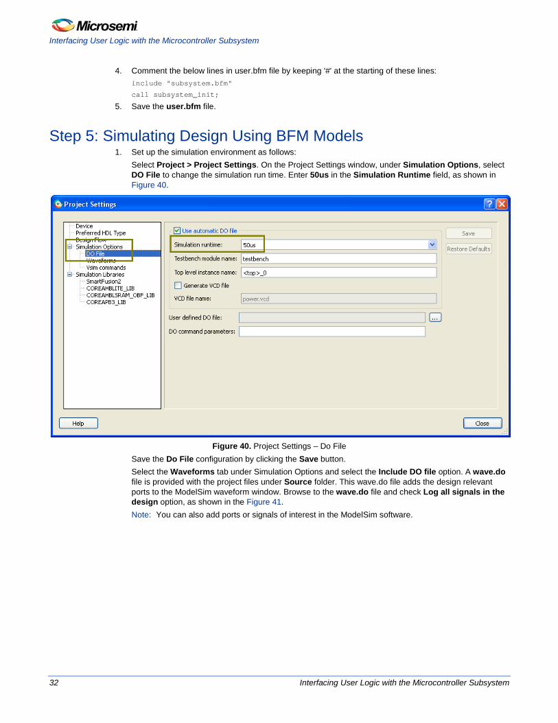
Step 5: Simulating Design Using BFM Models 1. Set up the simulation environment as follows:
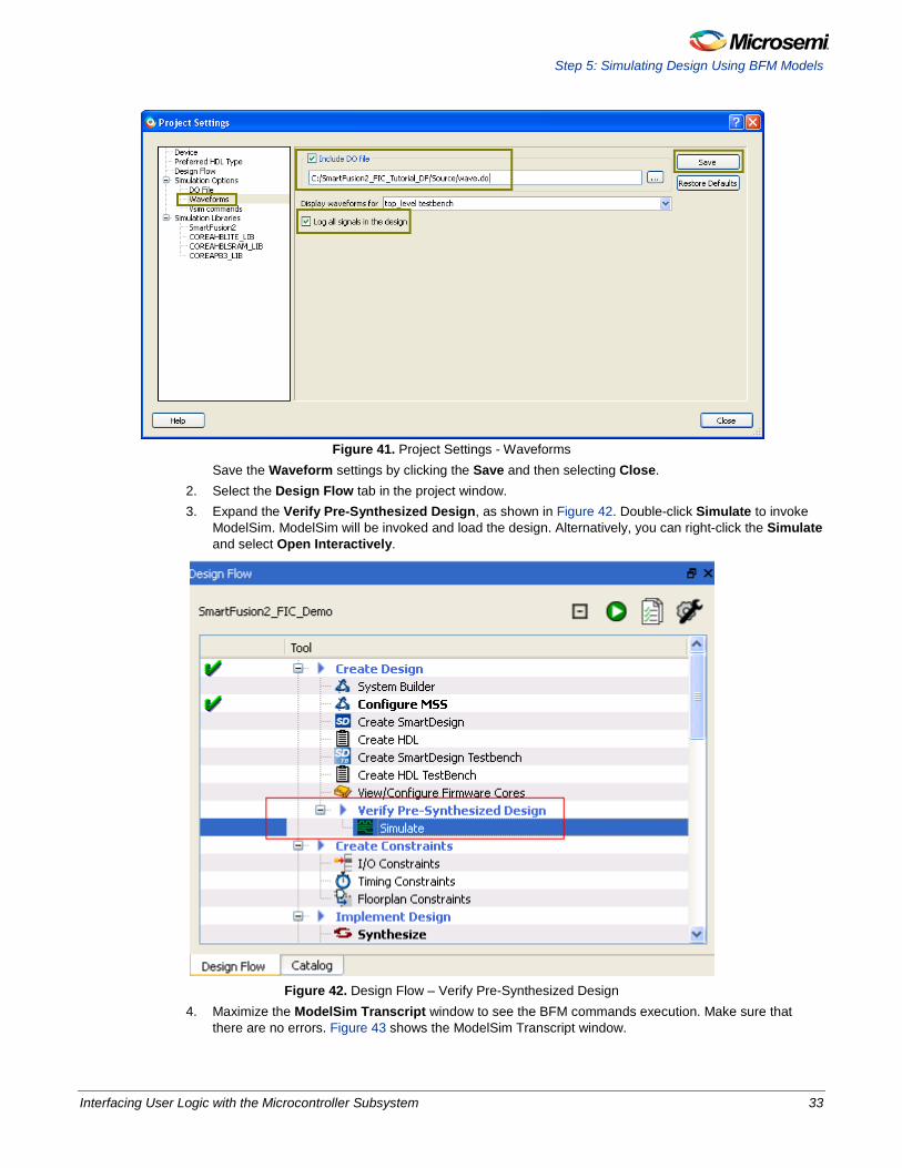
Select Project > Project Settings. On the Project Settings window, under Simulation Options, select DO File to change the simulation run time. Enter 50us in the Simulation Runtime field, as shown in Figure 40.
Figure 40. Project Settings – Do File
Save the Do File configuration by clicking the Save button. Select the Waveforms tab under Simulation Options and select the Include DO file option. A wave.do file is provided with the project files under Source folder. This wave.do file adds the design relevant ports to the ModelSim waveform window. Browse to the wave.do file and check Log all signals in the design option, as shown in the Figure 41. Note: You can also add ports or signals of interest in the ModelSim software.
Step 5: Simulating Design Using BFM Models
Interfacing User Logic with the Microcontroller Subsystem 33
Figure 41. Project Settings - Waveforms
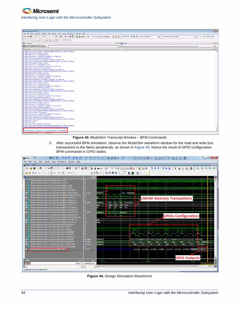
Save the Waveform settings by clicking the Save and then selecting Close. 2. Select the Design Flow tab in the project window. 3. Expand the Verify Pre-Synthesized Design, as shown in Figure 42. Double-click Simulate to invoke
ModelSim. ModelSim will be invoked and load the design. Alternatively, you can right-click the Simulate and select Open Interactively.
Figure 42. Design Flow – Verify Pre-Synthesized Design
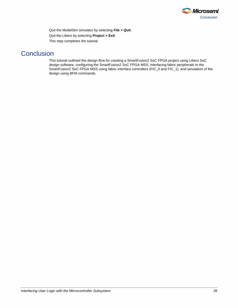
4. Maximize the ModelSim Transcript window to see the BFM commands execution. Make sure that there are no errors. Figure 43 shows the ModelSim Transcript window.
Interfacing User Logic with the Microcontroller Subsystem
34 Interfacing User Logic with the Microcontroller Subsystem
Figure 43. ModelSim Transcript Window – BFM Commands
5. After successful BFM simulation, observe the ModelSim waveform window for the read and write bus transactions to the fabric peripherals, as shown in Figure 44. Notice the result of GPIO configuration BFM commands in GPIO states.
Figure 44. Design Simulation Waveforms
Conclusion
Interfacing User Logic with the Microcontroller Subsystem 35
Quit the ModelSim simulator by selecting File > Quit. Quit the Libero by selecting Project > Exit. This step completes the tutorial.
Conclusion This tutorial outlined the design flow for creating a SmartFusion2 SoC FPGA project using Libero SoC design software, configuring the SmartFusion2 SoC FPGA MSS, interfacing fabric peripherals to the SmartFusion2 SoC FPGA MSS using fabric interface controllers (FIC_0 and FIC_1), and simulation of the design using BFM commands.

Interfacing User Logic with the Microcontroller Subsystem 37
List of Changes
Revision Changes Page
Revision 5 (April 2013)
Updated the document for 11.0 production SW release (SAR 47302). NA
Revision 4 (February 2013)
Updated the document for Libero 11.0 Beta SP1 software release (SAR 44868). NA
Revision 3 (November 2012)
Updated the document for Libero 11.0 Beta SPA software release (SAR 42904). NA
Revision 2 (October 2012)
Updated the document for Libero 11.0 Beta launch (SAR 41696). NA
Revision 1 (May 2012)
Updated the document for LCP2 software release (SAR 38954). NA
Note: The revision number is located in the part number after the hyphen. The part number is displayed at the bottom of the last page of the document. The digits following the slash indicate the month and year of publication.

Interfacing User Logic with the Microcontroller Subsystem 39
Product Support
Microsemi SoC Products Group backs its products with various support services, including Customer Service, Customer Technical Support Center, a website, electronic mail, and worldwide sales offices. This appendix contains information about contacting Microsemi SoC Products Group and using these support services.
Customer Service Contact Customer Service for non-technical product support, such as product pricing, product upgrades, update information, order status, and authorization.
From North America, call 800.262.1060 From the rest of the world, call 650.318.4460 Fax, from anywhere in the world 408.643.6913
Customer Technical Support Center Microsemi SoC Products Group staffs its Customer Technical Support Center with highly skilled engineers who can help answer your hardware, software, and design questions about Microsemi SoC Products. The Customer Technical Support Center spends a great deal of time creating application notes, answers to common design cycle questions, documentation of known issues and various FAQs. So, before you contact us, please visit our online resources. It is very likely we have already answered your questions.
Technical Support Visit the Microsemi SoC Products Group Customer Support website for more information and support (http://www.microsemi.com/soc/support/search/default.aspx). Many answers available on the searchable web resource include diagrams, illustrations, and links to other resources on website.
Website You can browse a variety of technical and non-technical information on the Microsemi SoC Products Group home page, at http://www.microsemi.com/soc/.
Contacting the Customer Technical Support Center Highly skilled engineers staff the Technical Support Center. The Technical Support Center can be contacted by email or through the Microsemi SoC Products Group website.
Email You can communicate your technical questions to our email address and receive answers back by email, fax, or phone. Also, if you have design problems, you can email your design files to receive assistance. We constantly monitor the email account throughout the day. When sending your request to us, please be sure to include your full name, company name, and your contact information for efficient processing of your request. The technical support email address is [email protected].
My Cases Microsemi SoC Products Group customers may submit and track technical cases online by going to My Cases.
Product Support
40 Interfacing User Logic with the Microcontroller Subsystem
Outside the U.S. Customers needing assistance outside the US time zones can either contact technical support via email ([email protected]) or contact a local sales office. Sales office listings can be found at www.microsemi.com/soc/company/contact/default.aspx.
ITAR Technical Support For technical support on RH and RT FPGAs that are regulated by International Traffic in Arms Regulations (ITAR), contact us via [email protected]. Alternatively, within My Cases, select Yes in the ITAR drop-down list. For a complete list of ITAR-regulated Microsemi FPGAs, visit the ITAR web page.


50200310-5/04.13
Microsemi Corporate Headquarters One Enterprise, Aliso Viejo CA 92656 USA Within the USA: +1 (949) 380-6100 Sales: +1 (949) 380-6136 Fax: +1 (949) 215-4996
Microsemi Corporation (NASDAQ: MSCC) offers a comprehensive portfolio of semiconductor solutions for: aerospace, defense and security; enterprise and communications; and industrial and alternative energy markets. Products include high-performance, high-reliability analog and RF devices, mixed signal and RF integrated circuits, customizable SoCs, FPGAs, and complete subsystems. Microsemi is headquartered in Aliso Viejo, Calif. Learn more at www.microsemi.com.
© 2013 Microsemi Corporation. All rights reserved. Microsemi and the Microsemi logo are trademarks of Microsemi Corporation. All other trademarks and service marks are the property of their respective owners.


![Usb Interfacing With Pic Microcontroller[Step by Step]](https://img.pdfslide.net/doc/110x75/563db7cd550346aa9a8e0eab/usb-interfacing-with-pic-microcontrollerstep-by-step.jpg)