Embed Size (px)
Citation preview
Interlayer exchange coupling in magnetic multilayers : asystematic experimental studyde Vries, J.J.
DOI:10.6100/IR470784
Published: 01/01/1996
Document VersionPublisher’s PDF, also known as Version of Record (includes final page, issue and volume numbers)
Please check the document version of this publication:
• A submitted manuscript is the author's version of the article upon submission and before peer-review. There can be important differencesbetween the submitted version and the official published version of record. People interested in the research are advised to contact theauthor for the final version of the publication, or visit the DOI to the publisher's website.• The final author version and the galley proof are versions of the publication after peer review.• The final published version features the final layout of the paper including the volume, issue and page numbers.
Link to publication
General rightsCopyright and moral rights for the publications made accessible in the public portal are retained by the authors and/or other copyright ownersand it is a condition of accessing publications that users recognise and abide by the legal requirements associated with these rights.
• Users may download and print one copy of any publication from the public portal for the purpose of private study or research. • You may not further distribute the material or use it for any profit-making activity or commercial gain • You may freely distribute the URL identifying the publication in the public portal ?
Take down policyIf you believe that this document breaches copyright please contact us providing details, and we will remove access to the work immediatelyand investigate your claim.
Download date: 09. Aug. 2018
Interlayer Exchange Coupling in Magnetic Multilayers
A systematic experimental study
PROEFSCHRIFT
ter verkrijging van de graad van doctor aan de Technische Universiteit Eindhoven, op gezag van de Rector Magnificus, prof. dr . M. Rem, voor een commissie aangewezen door het College van Dekanen in het openbaar te verdedigen op
donderdag 21 november 1996 om 16.00 uur
door
Jitze Jan de Vries
geboren te Groningen
Dit proefschrift is goedgekeurd door de promotoren:
prof. dr. ir. W.J.M. de Jonge prof. dr. ir. J.A. Pals
Co promo tor:
dr. ir. P.J.H. Bloemen
De Vries, Jitze Jan
Interlayer exchange coupling in magnetic multilayers, a systematic experimental study / Jitze Jan de Vries. - Eindhoven : Eindhoven University of Technology. Thesis Eindhoven University of Technology. - With bibliogr., ref. - With summary in Dutch. ISBN 90-386-0398-3
aan mijn ouders
The work described in this thesis has been performed within a cooperative contract between the Solid State Division (Cooperative Phenomena) of the Physics Department at the Eindhoven University of Technology and the Magnetism group at the Philips Research Laboratories Eindhoven (PRLE). The research has been carried out at the PRLE. The financial support by the Foundation for Fundamental Research on Matter (FOM) is gratefully acknowledged. Part of the research has been sponsored by the European Community science project ESPRIT3: Basic Research, 'Study of Magnetic Multilayers for Magnetoresistive Sensors'.
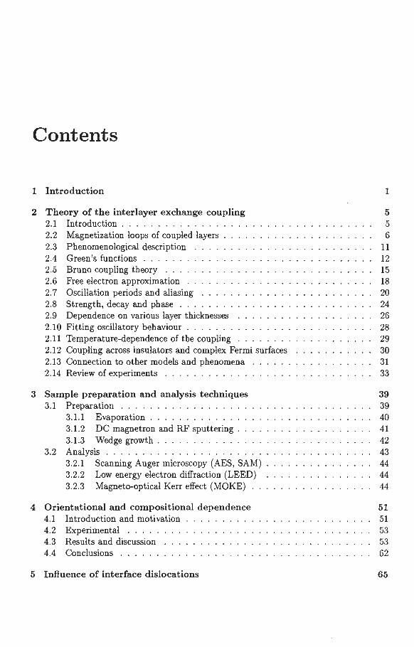
Contents
1 Introduction
2 Theory of the interlayer exchange coupling 2.1 Introduction ... .......... . 2.2 Magnetization loops of coupled layers 2.3 Phenomenological description 2.4 Green's functions ..... . 2.5 Bruno coupling theory ... . 2.6 Free electron approximation 2. 7 Oscillation periods and aliasing 2.8 Strength, decay and phase . . . 2.9 Dependence on various layer thicknesses 2.10 Fitting oscillatory behaviour . .. ... . 2.11 Temperature-dependence of the coupling 2.12 Coupling across insulators and complex Fermi surfaces 2.13 Connection to other models and phenomena 2.14 Review of experiments ............ .
3 Sample preparation and analysis techniques 3.1 PreparatiOn ................ .
3.1.l Evaporation ... ......... . 3.1.2 DC magnetron and RF sputtering . 3.1.3 Wedge growth ..... ...... .
3.2 Analysis .................. . 3.2.l Scanning Auger microscopy (AES, SAM) 3.2.2 Low energy electron diffraction (LEED) 3.2.3 Magneto-optical Kerr effect (MOKE)
4 Orientational and compositional dependence 4.1 Introduction and motivation 4.2 Experimental . .... 4.3 Results and discussion 4.4 Conclusions ... .. .
5 Influence of interface dislocations
1
5 5 6
11 12 15 18 20 24 26 28 29 30 31 33
39 39 40 41 42 43 44 44 44
51 51 53 53 62
65

5.1 Introduction and motivation 5.2 Experimental ... . . 5.3 Results and discussion 5.4 Conclusions . . . . . .
6 Magnetic layer thickness-dependence 6.1 Introduction and motivation 6.2 Experimental . .... 6.3 Results and discussion 6.4 Conclusions . . . . . .
7 Cap layer thickness-dependence 7.1 Introduction and motivation 7.2 Experimental . ... . 7.3 Results and discussion 7.4 Conclusions . . . .. .
8 Importance of matching Fermi surfaces 8.1 Introduction and motivation 8.2 Experimental ..... 8.3 Results and discussion 8.4 Conclusions . . . . . .
9 Interlayer coupling across 'semiconductors' 9.1 Introduction and motivation 9.2 Previous work ... . . 9.3 Experimental .... . 9.4 Results and discussion 9.5 Conclusions .... .
10 Summary and outlook
References
List of publications
Samenvatting
Dankwoord
Curriculum vitae
65 67 69 76
77 77 77 80 84
85 85 86 87 94
95 95 96 96
103
105 105 106 107 108 117
119
123
135
139
143
145

Chapter 1
Introduction.
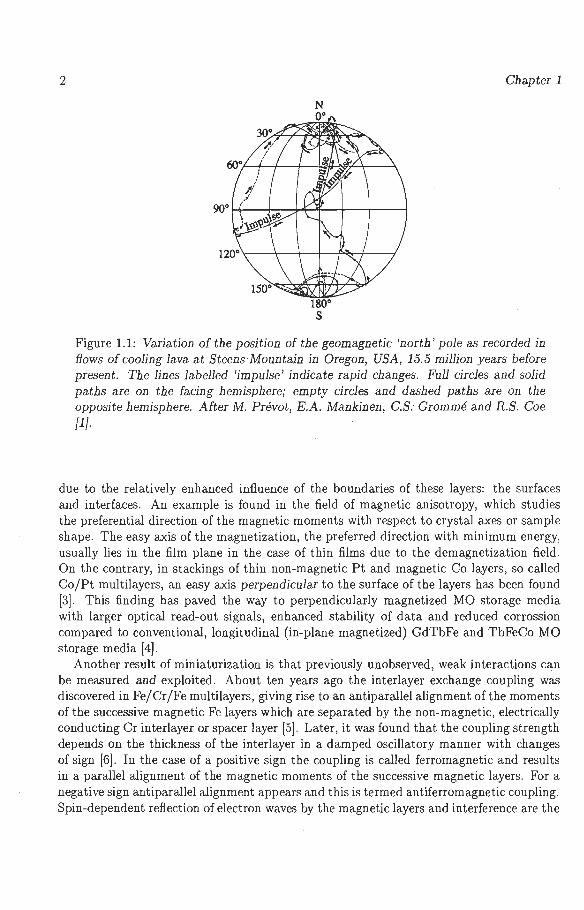
Over millions of years nature has been recording. the varying direction of the earth magnetic field in flows of cooling lava, see figure 1.1. The study of the history of the earth magnetic field via the magnetic moments in basaltic lava is called paleomagnetism. Volcanic eruptions have created flows of lava containing ferrimagnetic titanomagnetite Fe3_x Tix04 .
The magnetic moment of this titanomagnetite will become aligned with the geomagnetic field upon heating. Subsequential cooling 'freezes' this geomagnetic field direction. This is similar to the recording process in present-day magneto-optical (MO) disks where a focused laser beam provides the heat and a coil the field. From this we know that the earth magnetic field reverses its polarity every few thousand years. Sometimes, the rate of change found amounts to as much as 6° in one day or 50° in one year, compared to current values of 6° in 100 years [l , 2] .
Only the last few decades mankind has entered the field of magnetic recording, digital (for example applied to data storage on computer hard disks and credit cards) as well as analogous (on audio and video tape and copiers), and magnetic detection (e.g. used in traffic control and geopositioning systems). Nowadays various forms of research of magnetic phenomena exist, including palecimagnetism just mentioned. Research topics are: magnetic anisotropy, magnetic interlayer coupling, magnetoresistance, magneto-optical effects, etc.
A general trend in product development and research is miniaturization, driven by material cost reduction, product compactness and the quest for new applicable phenomena. In particular for magnetic recording, this trend is also pushed by the demand for higher data storage capacities. The process is stimulated by the advancement of modern preparation methods which offer the highly controlled deposition of thin films of material. MBE (molecular beam epitaxy) under ultra high vacuum conditions is one of the examples especially interesting for scientific investigations. More industrially oriented techniques like MOCVD (metal organic chemical vapour deposition) offer, in time, the same degree of control.
A perhaps trivial, first step is the reduction of the length scale in one dimension from three-dimensional bulk materials to more two-dimensional layers: for instance from a magnetic compass-needle to a magnetic tape, typically 0.1-1 µm thick . However, if the layer thicknesses are further reduced new phenomena with new applications may be expected
1
2
1so· s
Chapter 1
Figure 1.1: Variation of the position of the geomagnetic 'north' pole as recorded in flows of cooling lava at Steens Mountain in Oregon , USA, 15.5 million years before present. The lines labelled 'impulse' indicate rapid changes. Full circles and solid paths are on the facing hemisphere; empty circles and dashed paths are on the opposite hemisphere. After M. Prevot, E.A. Mankinen, C.S. Gromme and R.S. Coe fl}.
due to the relatively enhanced influence of the boundaries of these layers: the surfaces and interfaces. An example is found in the field of magnetic anisotropy, which studies the preferential direction of the magnetic moments with respect to crystal axes or sample shape. The easy axis of the magnetization, the preferred direction with minimum energy, usually lies in the film plane in the case of thin films due to the demagnetization field. On the contrary, in stackings of thin non-magnetic Pt and magnetic Co layers , so called Co/Pt multilayers, an easy axis perpendicular to the surface of the layers has been found [3] . This finding has paved the way to perpendicularly magnetized MO storage media with larger optical read-out signals, enhanced stability of data and reduced corrossion compared to conventional, longitudinal (in-plane magnetized) GdTbFe and TbFeCo MO storage media [4].
Another result of miniaturization is that previously unobserved, weak interactions can be measured and exploited. About ten years ago the interlayer exchange coupling was discovered in Fe/Cr/Fe multilayers, giving rise to an antiparallel alignment of the moments of the successive magnetic Fe layers which are separated by the non-magnetic, electrically conducting Cr interlayer or spacer layer [5]. Later, it was found that the coupling strength depends on the thickness of the interlayer in a damped oscillatory manner with changes of sign [6] . In the case of a positive sign the coupling is called ferromagnetic and results in a parallel alignment of the magnetic moments of the successive magnetic layers. For a negative sign anti parallel alignment appears and this is termed antiferromagnetic coupling. Spin-dependent reflection of electron waves by the magnetic layers and interference are the

Introduction 3
mechanisms behind this coupling. The more familiar dipole-dipole magnetic interaction mechanism which applies to the coupling between two compass-needles will never give rise to a 'ferromagnetic' coupling not to mention an oscillatory variation as a function of the distance, see frontpage. The interlayer exchange coupling mechanism can be applied in direct overwrite MO storage media [7] .
An other mechanism of spin-dependent scattering of conduction electrons underlies the giant magnetoresistance (GMR) effect as distinct from the conventional anisotropic magnetoresistance (AMR) effect. The former was discovered soon after the finding of interlayer exchange coupling [8, 9]. GMR implies that the conductivity or likewise the resistance of a magnetic multilayer depends on the alignment of the magnetic moments in successive layers. The magnetic layers form an obstacle for conduction electrons with a majority spin in the magetic layer, whereas electrons with the reversed spin can travel on more easily. For a parallel alignment of the moments in successive magnetic layers only electrons of one spin type can travel through the multilayer and the other is scattered at the interfaces, while for antiparallel alignment electrons of both spin types are scattered. As a result the resistance is high and low for antiparallel and parallel alignment, respectively, and the normalized resistance change can be as much as a 220 % [10] compared to an AMR effect of about 5 %. As the antiparallel alignment - e.g. due to antiferromagnetic interlayer exchange coupling - of the magnetic moments can be forced to become parallel by an external magnetic field emanating from a magnetic data storage medium or a permanent magnet, this effect has great potential for application in all kinds of magnetic devices: reading heads, magnetometers, position sensors, etc. Currently, eight years after the discovery, the first hard disk reading heads using GMR make their way to the market.
This thesis focuses on the physical mechanism underlying the interlayer exchange coupling, rather than its applications, and its behaviour is investigated by means of various experiments. First, the interlayer exchange coupling model developed by Bruno [11] will be presented (chapter 2) . His model is very transparent and comprises several other coupling models. Subsequently, in chapter 3, the experimental side of this work is explained, viz. the preparation of samples with uniform and wedge-shaped magnetic and non-magnetic layers by sputtering and evaporation in (ultra high) vacuum, the analysis of their growth and the magnetic characterization using the magneto-optical Kerr effect . Following this, experiments focusing on several aspects of the interlayer exchange coupling are discussed, such as: the orientational dependence of the interlayer exchange coupling (chapter 4), the effect of interface dislocations due to lattice mismatch (chapter 5), the dependence on the magnetic layer thickness (chapter 6) and cap layer thickness (chapter 7) and the importance of the match of Fermi surfaces of the interlayer and magnetic layer materials (chapter 8). Finally, an investigation of the coupling across a possible semiconductor is presented in chapter 9. All experimental results are confronted with the theoretical predictions. To conclude, the main results are summarized and some suggestions for future research are given in chapter 10.
4 Chapter 1
Chapter 2
Theory of the interlayer exchange coupling
Abstract
In this chapter, the theory of the interlayer exchange coupling will be explained with emphasis on the Bruno coupling model. First, it is shown how magnetization loops can be calculated by considering the field, anisotropy and coupling energy contributions. Furthermore, it is indicated how the coupling strength can be determined from experimental hysteresis loops. Before presenting the Bruno coupling model, a phenomenological description is given and some properties of Green's functions are highlighted as these functions play an important role in the derivation. In relation to the experiments that were carried out, several aspects of the theory are treated in the following sections. The chapter concludes with a discussion of other models of interlayer exchange coupling and other effects with the same underlying mechanism and a review of the experimental results obtained so far.
2 .1 Introduction
The phenomenon of interlayer exchange coupling may be observed when two magnetic layers are brought closely together, but are still separated by an interlayer or spacer layer, typically 10 A thick. A stacking of Fe/Cr/Fe layers for example could display interlayer coupling. It was in fact a repeated stacking of Fe/Cr/Fe, a multilayer , in which Grunberg et al. discovered the effect using Brillouin light scattering (BLS) [5]. By assuming an interaction that favours an antiparallel alignment of the moments in successive magnetic layers, they could explain their experimental results. Later, Parkin et al. showed that the interaction oscillates in magnitude as a function of the spacer layer thickness [12). They deduced the coupling strength from hysteresis loops and magnetoresistance measurements. An oscillation between parallel and antiparallel alignment (an oscillation of the sign in fact) was established by Demokritov et al. [6] .
5
2. 2 Magnetization loops of coupled layers
It is clear that the action of a coupling that favours antiparallel alignment opposes the action of a magnetic field which ultimately enforces a parallel alignment. Qualitatively, the stronger the coupling, the larger the fields required to reach this state of parallel alignment. It is the purpose of this section to derive a quantitative relation.
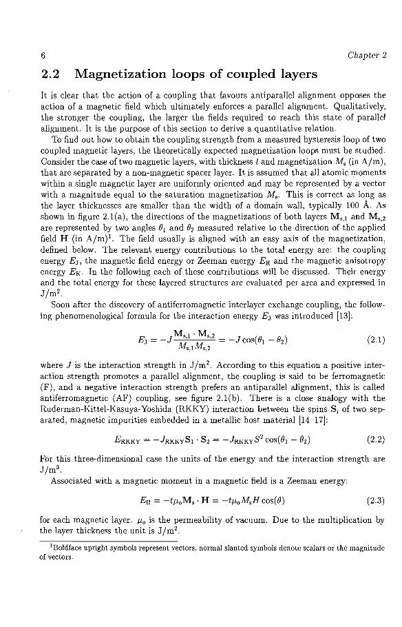
To find out how to obtain the coupling strength from a measured hysteresis loop of two coupled magnetic layers, the theoretically expected magnetization loops must be studied. Consider the case of two magnetic layers, with thickness t and magnetization Ms (in A/m), that are separated by a non-magnetic spacer layer. It is assumed that all atomic moments within a single magnetic layer are uniformly oriented and may be represented by a vector with a magnitude equal to the saturation magnetization Ms. This is correct as long as the layer thicknesses are smaller than the width of a domain wall, typically 100 A. As shown in figure 2.l(a), the directions of the magnetizations of both layers Ms,! and Ms,2
are represented by two angles 01 and 02 measured relative to the direction of the applied field H (in A/m) 1 . The field usually is aligned with an easy axis of the magnetization, defined below. The relevant energy contributions to the total energy are: the coupling energy EJ, the magnetic field energy or Zeeman energy Ett and the magnetic anisotropy energy EK. In the following each of these contributions will be discussed. Their energy and the total energy for these layered structures are evaluated per area and expressed in J/m2.
Soon after the discovery of antiferromagnetic interlayer exchange coupling, the following phenomenological formula for the interaction energy EJ was introduced [13]:
Ms1 · M.2 EJ = -J M M ' = -Jcos(B1 - 02 )
s,l s,2 (2.1)
where J is the interaction strength in J /m2. According to this equation a positive interaction strength promotes a parallel alignment, the coupling is said to be ferromagnetic (F), and a negative interaction strength prefers an antiparallel alignment, this is called antiferromagnetic (AF) coupling, see figure 2.l(b). There is a close analogy with the Ruderman-Kittel-Kasuya-Yoshida (RKKY) interaction between the spins Si of two separated, magnetic impurities embedded in a metallic host material [14-17]:
(2.2)
For this three-dimensional case the units of the energy and the interaction strength are J/m3.
Associated with a magnetic moment in a magnetic field is a Zeeman energy:
(2.3)
for each magnetic layer. µ 0 is the permeability of vacuum. Due to the multiplication by the layer thickness the unit is J/m2 .
1 Boldface upright symbols represent vectors, normal slanted symbols denote scalars or the magnitude of vectors.

Theory of the interlayer exchange coupling
(a) (b)I DiMs,1 I l:'liMs,1 I
H J>O J<O
Ms,2 l'liMs,2 I I Ms,2 .i
Figure 2.1: (a) Definition of the angles 81 and 82 of the magnetizations Ms,I and Ms,2 of the two magnetic layers with the applied field H. (b) Two exchange coupled magnetic layers with the direction of the magnetizations indicated by the arrows. Parallel alignment results for ferromagnetic (F) coupling (J > 0) and antiparallel coupling results in the case of antiferromagnetic (AF) coupling (J < 0).
7
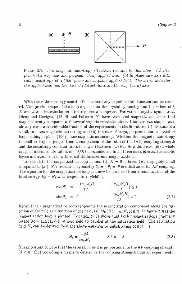
The energy contribution of the magnetic anisotropy depends on the crystal symmetry and the shape of the sample. In general, to describe the dependence in three dimensions, two angles and several terms of increasing order are required. However, usually the first order anisotropy term dominates higher order terms which may therefore be omitted. Furthermore, a description with one angle often suffices in the case of a thin film. There are two important situations: a perpendicular easy axis or an in-plane easy axis, see figure 2.2. For a perpendicular easy axis the anisotropy energy is given by:
(2.4)
where 81- is the angle subtended by the magnetization vector and the film normal and K1-is the anisotropy constant in J/m3 (K1- > 0 J/m3 ). For an in-plane easy axis (K1- < 0 J/m3 ) the magnetization lies in-plane 81- = 7r/2, EK,1- = 0 J/m2. The anisotropy energy is then determined by the next term, the anisotropy in the plane of the film, usually the magnetocrystalline anisotropy. The magnetocrystalline anisotropy energy of a bulk crystal with cubic anisotropy is, to lowest order:
(2.5)
where EK,cubic and Kcubic both have the unit J/m3 and ai are the direction cosines relative to the [100] crystal axes. This relation is now subject to the restriction 81- = 7r /2 and must be rewritten as a function of 811, the angle in the plane. Note that the expressions of ai(81-,811) depend on the orientation. For a cubic anisotropy and a (100)-plane one obtains:
(2.6)
where 811 is measured relative to an in-plane easy axis. The angles 81- and 811 for which equations (2.4) and (2.6) reach their absolute minimum energy, define the easy axes of the magnetization (dashed lines in figure 2.2). Likewise the angles 81- and 811 yielding an absolute maximum energy, define the hard axes of the magnetization (dotted lines in figure 2.2). For all hysteresis loops in this thesis the magnetic field was applied along one of the easy axes.
8 Chapter 2
"··................ . ...... ....
"--~)+(,- H
(b)
... ····· ··· .....
Figure 2.2: Two magnetic anisotropy situations relevant to thin films. (a) Perpendicular easy axis and perpendicularly applied field. (b) In-plane easy axis with cubic anisotropy of a (100)-plane and in-plane applied field. The arrow indicates the applied field and the dashed (dotted) lines are the easy (hard) axes.
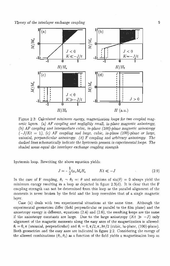
With these three energy contributions almost any experimental situation can be covered . The precise shape of the loop depends on the crystal symmetry and the values of t, K and J and its calculation often requires a computer. For various crystal symmetries, Dieny and Gavignan [18, 19] and Folkerts [20] have calculated magnetization loops that may be directly compared with several experimental situations. However, two simple cases already cover a considerable fraction of the experiments in the literature: (i) the case of a small , in-plane magnetic anisotropy and (ii) the case of large, perpendicular, uniaxial or large, cubic, in-plane (100)-plane magnetic anisotropy. Whether the magnetic anisotropy is small or large is judged from a comparison of the ratio of the (AF) coupling strength and the anisotropy constant times the layer thickness -J /Kt . As a third case (iii) a whole range of intermediate values of -J /Kt is considered . In all three cases identical magnetic layers are assumed, i.e. with equal thicknesses and magnetizations.
To calculate the magnetization loop in case (i), K = 0 is taken (Kt negligibly small compared to IJI). For reasons of symmetry 81 = -82 =: 8 is substituted for AF coupling. The equation for the magnetization loop can now be obtained from a minimization of the total energy EH+ EJ with respect to 8, yielding:
cos(8) =
sin(8) 0 (2.7)
Recall that a magnetization loop represents the magnetization component along the direction of the field as a function of the field, i.e. MH(H) = µ 0 M. cos(8). In figure 2.3(a) the magnetization loop is plotted . Equation (2.7) shows that both magnetizations gradually rotate from antiparallel at zero field to parallel at the saturation field . The saturation field H 8 can be derived from the above equation by substituting cos(8) = 1:
-2J H.=-
tµoMs Kt« -J (2.8)
It is important to note that the saturation field is proportional to the AF coupling strength (J < 0), thus providing a means to determine the coupling strength from an experimental
Theory of the interlayer exchange coupling
1 (a) 1 (b)
i 0 i 0 - -~ ~ ,-J<O I J<O K«-Jft I K=-Jt -1 -1 _,
0 1 -1 0 1
H/H. H/Hr
1 (c) 1 (d)
i 0 i 0 - -~ ~ J<O
I
K»-J/t J>O -1 .! -1 -1 0 1 0
H/Hr H (a.u.)
Figure 2.3: Calculated minimum energy, magnetization loops for two coupled magnetic layers. (a) AF coupling and negligibly small, in-plane magnetic anisotropy, (b) AF coupling and intermediate cubic, in-plane (100)-plane magnetic anisotropy (-J/Kt = 1), (c) AF coupling and large, cubic, in-plane (100)-plane or large, uniaxial, perpendicular anisotropy. (d) F coupling and arbitrary anisotropy. The dashed lines schematically indicate the hysteresis present in experimental loops. The shaded areas equal the interlayer exchange coupling strength
hysteresis loop. Rewriting the above equation yields:
9
Kt« -J (2.9)
In the case of F coupling, 81 = 82 =: B and solutions of sin(B) = 0 always yield the minimum energy resulting in a loop as depicted in figure 2.3(d). It is clear that the F coupling strength can not be determined from this loop as the parallel alignment of the moments is never broken by the field and the loop resembles that of a single magnetic layer.
Case (ii) deals with two experimental situations at the same time. Although the experimental geometries differ (field perpendicular or parallel to the film plane) and the anisotropy energy is different , equations (2.4) and (2.6) , the resulting loops are the same if the anisotropy constants are large. Due to the large anisotropy (Kt » -J) only alignment of the magnetic moments along the easy axes of the magnetization is allowed: B; = 0, ?r (uniaxial, perpendicular) and Bi= 0,?r/2,?r,37r/2 (cubic, in-plane, (100)-plane). Both geometries and the easy axes are indicated in figure 2.2. Considering the energy of the allowed combinations (81 , 82 ) as a function of the field yields a magnetization loop as
10 Chapter 2
in figure 2.3(c). The sharp transition where the saturated state is reached is called the flip field Hr. In fact saturation field would also be correct, but that term was already used for the gradual transition in case (i) . The flip field in this case equals:
-J Hr=-. - Kt » -J (2.10)
tµoMs
which can be rewritten to calculate the AF coupling strength from the coupling field of an experimental hysteresis loop
Kt » -J (2.11)
F coupling would again result in the loop of figure 2.3(d) . For intermediate values of -J /Kt numerical calculations are usually required to obtain
a magnetization loop. An example of such a loop for -J /Kt = 1 and a cubic in-plane (100)-plane anisotropy is given in figure 2.3(b) . The steep transition to the saturated state appears at the flip field Hr. A simple relation between the flip field and the coupling strength does not exist for intermediate values of -J /Kt. In figure 2.4 -tµ 0 M,Hr / J is plotted against -J/Kt. In the two limiting cases (i) and (ii) -tµ0 MsHrf J approaches 2 and 1, respectively, in agreement with equations (2.9) and (2.11). For intermediate cases a continuous transition between these two limiting cases takes place.
Alternatively, if all higher order terms vanish in equation (2.26) , the bilinear coupling strength may be defined as: ·
(2.12)
which corresponds to the shaded areas in figure 2.3. EAF (EF) is the magnetic energy associated with the AF (F or un-) coupled loop. The arrow subscripts indicate the alignment of the two coupled magnetic layers. In all AF coupled cases the same area is found (this is not directly clear from the figure) if the coupling strength is the same. However, this method is incompatible with the MOKE measurement technique, see subsection 3.2.3.
In an attempt to find a field from which the coupling strength can be obtained with one single equation, one may define the half field H .!. . The half field is the field where the
2
magnetization reaches half its saturation value H~ = H(!Ms)· To obtain the coupling strength J = -tµ 0 M,H.!. is used. The curve in figure 2.4 shows that in the limiting cases
2
the coupling strength is correctly obtained but for -J/Kt = 1 a maximum deviation of 30 % is present. In the case of unequal layer thicknesses or magnetizations the half field is defined as H.!. = H(!Mn +!Mu) . In the antiparallel alignment state Uthe magnetic layer with the farger moment is assumed to have its moment aligned with the field.
As minimum energy calculations have been used these loops do not display hysteresis. For this reason the calculated loops have been called magnetization loops and the experimental loops have been referred to as hysteresis loops. In order to obtain the correct coupling strength from the saturation , flip or half field one must average over the hysteresis. In other words one must estimate the solid lines from the dashed ones in figure 2.3. Although a few exceptional cases exist where the hysteresis is asymmetric and a simple averaging yields a wrong result , in most cases averaging over the hysteresis is sufficient [18-20].

Theory of the interlayer exchange coupling
1 I-~-..... -=-~-=-=--=- - - - - - - - - - - _;;;-;:_-::_:-...---!
-J/Kt
Figure 2.4: Ratio of the calculated and preset coupling strength versus the ratio -J /Kt for a cubic in-plane (100)-plane anisotropy. The coupling strength is calculated from the saturation or flip field and from the half field obtained from numerically calculated minimum energy magnetization loops.
2.3 Phenomenological description
11
Up to now the mechanism of the interlayer exchange coupling, that determines the value of J, has not been discussed. In fact, several mechanisms of coupling between two separated, magnetic layers exist, like magnetostatic coupling through dipolar fields or pinhole coupling through ferromagnetic bridges in the spacer layer. This work focuses on another coupling type which dominates the previous coupling contributions in fiat, homogeneous, magnetic multilayers: the interlayer exchange coupling.
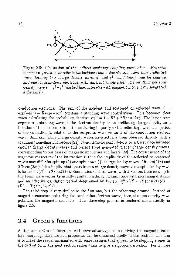
The close analogy between equations (2.1) and (2.2) is not fortuitous and it is not surprising that the first interlayer exchange coupling models were developed from the RKKY theory [21]. As will become clear, the interlayer exchange coupling and the RKKY exchange coupling between magnetic impurities in a metallic host are based on the same physical mechanism. This mechanism is the mediation of magnetic 'information' between magnetic moments via the spin of the conduction electrons in the spacer or host material. For this reason the interaction is sometimes called indirect exchange coupling in contrast with the direct exchange coupling between neighboring magnetic atomic moments within a ferromagnet. The interaction takes place in three steps.
The first step is an interaction between conduction electrons in the host material or the spacer layer and localized electrons responsible for the net moment of the magnetic impurities or the magnetic layers. The former electrons are represented by plane wave functions 'I/; = exp( +ikr) (Bloch waves), and interact with the latter. Due to the interaction, the incident conduction electron wave is scattered or reflected into a wave 'I/; = R exp( -ikr).
To understand the second step it is important to consider the wave nature of the
12 Chapter 2
Figure 2.5: Illustration of the indirect exchange coupling mechanism. Magnetic moment m 1 scatters or reflects the incident conduction electron waves into a reflected wave, forming two charge density waves qT and ql (solid lines), one for spin-up and one for spin-down electrons, with different amplitudes. The resulting net spin density waves= qT -ql (dashed line) interacts with magnetic moment m 2 separated a distance r.
conduction electrons. The sum of the incident and scattered or reflected wave '!/; = exp( +ikr) + Rexp(-ikr) contains a standing wave contribution. This becomes clear when calculating the probability density: '!/;'!/;* = 1 + R2 + 2R cos(2kr ). The latter term expresses a standing wave in the electron density or an oscillating charge density as a function of the distance r from the scattering impurity or the reflecting layer. The period of the oscillation is related to the reciprocal wave vector k of the conduction electron wave. Such oscillating charge density waves have actually been observed directly with a scanning tunnelling microscope [22]. Non-magnetic point defects on a Cu surface initiated circular charge density waves and terrace steps generated planar charge density waves, corresponding to our cases of magnetic impurities and layers [22]. The consequence of the magnetic character of the interaction is that the amplitude of the reflected or scattered waves may differ for spin-up (I) and spin-down(!) charge density waves: 2RT cos(2kr) and 2Rl cos(2kr). This implies that apart from a charge density wave also a spin density wave is formed: 2(RT - Rl) cos(2kr). Summation of these waves with k-vectors from zero up to the Fermi wave vector kF usually results in a decaying amplitude with increasing distance and an effective oscillation period determined by kF, e.g. JtF 2(RT - Rl) cos(2kr )dk = (RT - Rl)sin(2kFr)/r.
The third step is very similar to the first one, but the other way around. Instead of magnetic moments polarizing the conduction electron waves, here, the spin density wave polarizes the magnetic moments. This three-step process is rendered schematically in figure 2.5.
2.4 Green's functions
As the use of Green's functions will prove advantageous in deriving the magnetic interlayer coupling, their use and properties will be discussed briefly in this section. The aim is to make the reader acquainted with some features that appear to be stepping stones in the derivation in the next section rather than to give a rigorous derivation. For a more
Theory of the interlayer exchange coupling 13
elaborate introduction the reader is referred to textbooks, e.g. [23] . For the present purpose a Green's function G can be defined as a solution of the fundamental inhomogeneous differential equation of the type:
(c - O(r))G(r, r', c) = 8(r - r') (2.13)
where O(r) is a time-independent, Hermitian, differential operator, 8 is the delta-function, rand r' are coordinates and c is a complex variable. The physical meaning of G(r, r', c) depends on the operator 0. For instance if 0 is the Laplace electrostatic potential operator then G represents the electric field at r due to a unit space charge localized at r'. If 0 is the Hamiltonian H 0 of a free particle then G represents the probability for a particle at position r to travel to a new position r' .
With help of the example of the Green's function of a free particle in one dimension the general properties of Green's functions that will be used later on, are introduced. The Green's function can be obtained by solving:
(c - H0 )G0 (x, x' , c) = (c + .!:!_ dd2
2 )G(x, x', c) = 8(x - x')
2m x
and is given by the following equation:
Go(x, x', c) = i:,2 exp(iklx - x'I)
(2.14)
(2.15)
with k = JI!i!j. The real part of c represents the energy l of the particle as expected for the Hamilton operator and k is the wave vector of the particle.
The power of Green's functions is that various other properties can simply be derived from it. For example, the density of states is given by [23]:
1 = =F-Tr Im G±(x, x, t:) 7f
= 1 rm 1fn v~
(2.16)
(2.17)
where Tr indicates the integration over x and Im that the imaginary part must be taken. Furthermore, use was made of:
G±(x, x', t:) = lim G(x, x', c) C--+f±tO+
(2.18)
for l ;::: 0 and with o+ representing an infinitesimal, positive, real value. Having found the Green 's function G0 of the unperturbed operator H 0 , this can be
used to obtain the perturbed Green's function G of the operator H = H 0 + H 1 with perturbation H 1:
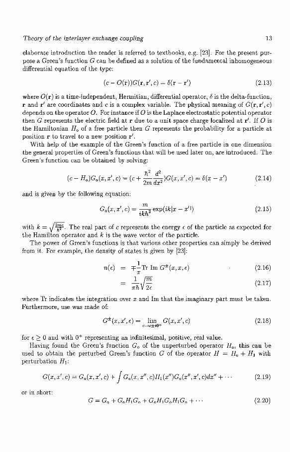
G(x,x',c) = G0 (x,x',c) + j G0 (x,x 11 ,c)H1(x")G0 (x 11 ,x', c)dx11 + · · · (2.19)
or in short: (2.20)
14 Chapter 2
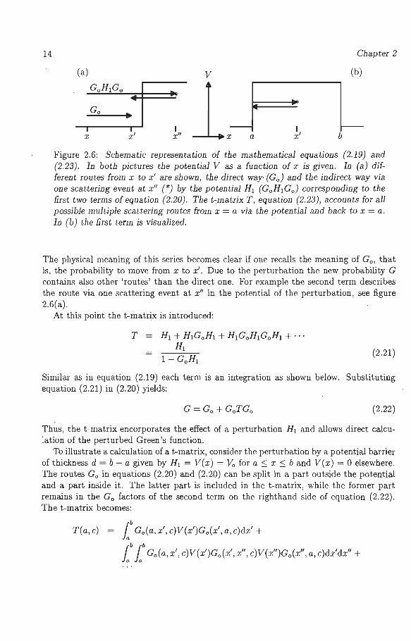
(a) v (b)
GoH1Go
lx Go .. I I
x x' x" a x' b
Figure 2.6: Schematic representation of the mathematical equations (2.19) and (2.23). In both pictures the potential V as a function of x is given. In (a) different routes from x to x' are shown , the direct way (G0 ) and the indirect way via one scattering event at x" (*) by the potential H 1 (G0 H 1G0 ) corresponding to the first two terms of equation (2.20). The t~matrix T, equation (2.23), accounts for all possible multiple scattering routes from x =a via the potential and back to x = a. In (b) the first term is visualized.
The physical meaning of this series becomes clear if one recalls the meaning of G0 , that is, the probability to move from x to x' . Due to the perturbation the new probability G contains also other 'routes' than the direct one. For example the second term describes the route via one scattering event at x" in the potential of the perturbation, see figure 2.6(a) .
At this point the t-matrix is introduced:
T H1 + H1GoH1 + H1G~H1GoH1 + ... H1
(2.21) 1- G0 H1
Similar as in equation (2.19) each term is an integration as shown below. Substituting equation (2.21) in (2.20) yields:
(2.22)
Thus, the t-matrix encorporates the effect of a perturbation H1 and allows direct calculation of the perturbed Green's function.
To illustrate a calculation of at-matrix, consider the perturbation by a potential barrier of thickness d = b - a given by H1 = V(x) = V0 for a::; x::; band V(x) = 0 elsewhere. The routes G0 in equations (2.20) and (2.20) can be split in a part outside the potential and a part inside it. The latter part is included in the t-matrix, while the former part remains in the G0 factors of the second term on the righthand side of equation (2.22). The t-matrix becomes:
T(a,c) = t G0 (a , x 1 ,c)V(x')G0 (x',a,c)dx1 +
lb t G0 (a , x' , c)V(x')G0 (x', x", c)V(x11 )G0 (x 11, a, c)dx'dx" +
Theory of the interlayer exchange coupling 15
1i2k [exp(2ikd)-1(-2mV0 )
-im 4 n2k2 + 2+2exp(2ikd)(2ikd-1)(-2mV0 ) 2 ···]
16 1i2k2 + (2.23)
Similar as in equation (2.19) all terms represent routes from a to a via multiple scattering by the perturbation H1 . For example, the first term represents the effect of travelling from a to all possible x' with a < x' < b, where scattering by the potential takes place, and subsequentially returning from x' to a, as is schematically depicted in figure 2.6(b). As a result the t-matrix concentrates the effect of the whole perturbation H1 in one single point x =a. In the limit d-+ oo the exponents average out and equation (2.23) becomes
a power series of ~2,:{ equal to JI - ~2,:{. By defining q = kJI - ~2_0• = {r,;-(f. - V0 ),
the t-matrix for a potential step is:
- ik1i2
(k - q) Too - -- ---m k+q
(2.24)
Compare this with a calculation of the reflection coefficient for a potential step by matching the wave functions and the first derivatives on either side of the step - compare equation (2.41) and see textbooks on quantum-mechanics e.g. [24] :
k-q Too= --
k+q (2.25)
Apart from a prefactor the t-matrix may be interpreted as representing the effective reflection coefficient resulting from multiple scattering by the perturbation.
Comparison of equations (2.15) and (2.24) shows that the prefactors cancel each other in the product of G and T . In this product the Green's functions account for the phase accumulation between scattering events and the t-matrix accounts for the reflection coefficients due to a scattering event. This notion and equations (2.16) and (2.22) in this section are important in the derivation of the general coupling expression due to Bruno [11].
2.5 Bruno coupling theory
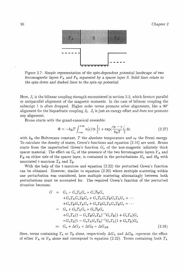
For the derivation of the coupling equation Bruno considers the effect of the perturbation of two ferromagnetic layers FA and F8 on the unperturbed states of a non-magnetic infinitely thick spacer material S. Associated with each layer FA , F8 and S is a certain (spin-dependent) potential, schematically shown in figure 2.7. The magnetic moments of both layers subtend an angle B. Each ferromagnetic layer may consist of several magnetic layers with different potentials and may be semi-infinitely thick. The effect of the perturbation on the total energy is calculated. This energy will depend on cos(B) and can be compared with:
E( B) = 10 + 11 cos B + 12 cos2 B + · · · (2.26)
16 Chapter 2
-----i 1-------------·
Figure 2.7: Simple representation of the spin-dependent potential landscape of two ferromagnetic layers FA and F8 separated by a spacer layerS. Solid lines relate to the spin-down and dashed lines to the spin-up potential.
Here, J1 is the bilinear coupling strength encountered in section 2.2, which favours parallel or antiparallel alignment of the magnetic moments. In the case of bilinear coupling the subscript 1 is often dropped. Higher order terms promote other alignments, like a 90° alignment for the biquadratic coupling }z. } 0 is just an energy offset and does not promote any alignment.
Bruno starts with the grand-canonical ensemble:
l +oo [ €F- € ] <I> = -k8 T -oo n( t) In 1 + exp( kaT ) dt (2.27)
with ka the Boltzmann constant, T the absolute temperature and EF the Fermi energy. To calculate the density of states, Green's functions and equation (2 .16) are used . Bruno starts from the unperturbed Green's function Go of the non-magnetic infinitely thick spacer material. The effect on G0 of the presence of the two ferromagnetic layers FA and F8 on either side of the spacer layer, is contained in the perturbations HA and H 8 with associated t-matrices TA and Ta.
With the help of the t-matrices and equation (2.22) the perturbed Green's function can be obtained. However, similar to equation (2 .20) where multiple scattering within one perturbation was considered, here multiple scattering alternatingly between both perturbations must be accounted for. The required Green's function of the perturbed situation becomes:
G = Go+ GoTAGo + GoTaGo
+GoTAGoTaGo + GoTAGoTaGoTAGo + · · · +GoTaGoTAGo + GoTaGoTAGoTaGo + · · · Go+ GoTAGo + GoTBGo
+GoTA(1- GoTaGoTA)- 1GoTB(1 + GoTA)Go
+GoTB(1- GoTAGoTBt 1GoTA(1 + GoTB)Go
- · Go+ f::!.GA + f::!.GB +~:!.GAB (2.28)
Here, terms containing TA or T8 alone, respectively I::!.G A and I::!.G 8 , represent the effect of either FA or F 8 alone and correspond to equation (2.22). Terms containing both TA
Theory of the interlayer exchange coupling 17
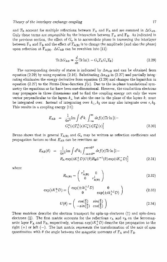
and TB account for multiple reflections between FA and FB and are summed in ~GAB· Only these terms are responsible for the interaction between FA and FB. As indicated in the previous section, the effect of G0 is to accumulate phase in traversing the interlayer between FA and FB and the effect ofTA(B) is to change the amplitude (and also the phase) upon reflection at F A(B)- ~GAB can be rewritten into [11]:
(2.29)
The corresponding density of states is indicated by ~nAB and can be obtained from equation (2.29) by using equation (2.16). Substituting ~nAB in (2 .27) and partially integrating eliminates the energy derivative from equation (2.29) and changes the logarithm in equation (2.27) to the Fermi-Dirac-function f(l) . Due to the in-plane translational symmetry the equations so far have been one-dimensional. However, the conduction electrons may propagate in three dimensions and to find the coupling energy not only the wave vector perpendicular to the layers kl. but also the one in the plane of the layers k11 must be integrated over. Instead of integrating over kl., k11 one may also integrate over €, k11. This results in a coupling energy [11] :
~Im j d2k11 j"" d€f(€)Trln [1-47r -00
G:(€)Tt(€)G:( €)Tit(€)) (2.30)
Bruno shows that in general TA(B) and G0 may be written as reflection coefficients and propagation factors so that EAB can be rewritten as:
(2.31)
where
( Tl(B) 0 )
RA(B) = 0 l TA(B)
(2.32)
ex (iK±D) = ( exp(±ik~ · t D) 0 ) P l. 0 exp(±ik~· 1 D)
(2 .33)
U(O) = ( co~(~J sin(j) ) -sm(2 ) cos( 2)
(2.34)
These matrices describe the electron transport for spin-up electrons (i) and spin-down electrons (!). The first matrix accounts for the reflections TA and TB. on the ferromagnetic layer FA and FB, respectively, whereas exp(iKf D) describe the propagation to the right ( +) or left ( - ) . The last matrix represents the transformation of the axis of spin quantization with () the angle between the magnetic moments of FA and F B·
18 Chapter 2
Usually one has kf := k't·' = k't· 1, i.e. a non-magnetic interlayer, yielding the following expression for the coupling energy:
with ql. = k1 - kJ.. (see section 2.7) and:
'F A(B) 1 T 1 2(r A(B) + r A(B))
1 T 1 2(r A(B) - r A(B))
(2.35)
(2.36)
(2.37)
the spin average and spin difference of the reflection coefficients. The trace of the logarithm has been calculated by writing the logarithm as a power series. After taking the trace, the sum of the two diagonal elements of the matrix, one obtains a power series which may be written again as a logarithm. Expanding equation (2 .35) in powers of cos(} and comparing with equation (2.26) , yields the bilinear 11, biquadratic 12 and higher order coupling terms (n 2: 1):
In = ~~Im j d2k111_: dcf(c)
1 [ 26.rAD.rseiql.D Jn ~ 1- 2rA'Fseiql.D + (rA2 - D.r~)(rs2 - D.r~)e2inD
(2.38)
The term 10 , which is equal to 11, represents a non-magnetic coupling constant as it does not contain any B-dependence and does not contribute to the coupling.
By using Green's functions explicit expressions for the coupling constants In have been found in terms of reflection coefficients, equations (2.36) and (2.37) , and propagation factors eiql.D and e2iql.D. The analogy with reflection and propagation was already indicated in section 2.4. However, to calculate the reflection coefficients one does not need to follow the procedure of the t-matrix but can choose much simpler methods.
2.6 Free electron approximation
In principle, equation (2.38) can be used to calculate the interlayer exchange coupling for a given band structure by evaluating the reflection coefficients for all k 11 and E or k
11
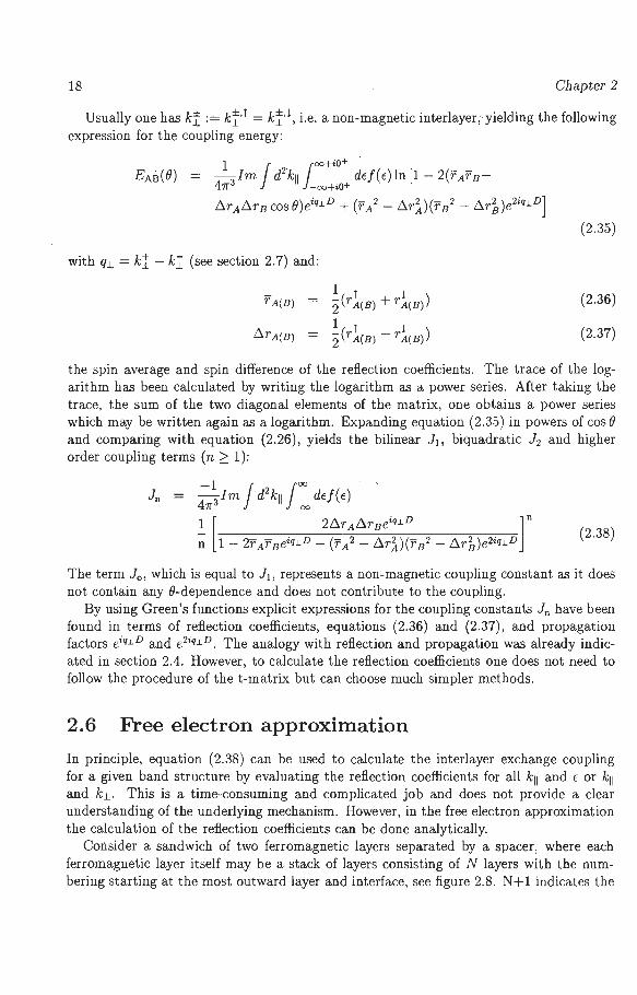
and kJ. . This is a time-consuming and complicated job and does not provide a clear understanding of the underlying mechanism. However, in the free electron approximation the calculation of the reflection coefficients can be done analytically.
Consider a sandwich of two ferromagnetic layers separated by a spacer, where each ferromagnetic layer itself may be a stack of layers consisting of N layers with the numbering starting at the most outward layer and interface, see figure 2.8. N+l indicates the
Theory of the interlayer exchange coupling 19
R; r;
.. .. .. ks,1- = k
k;,.l. N+l,.l. ••
j.
•
r T r Vi
r l T V=O Vi
t .... .... .. Ill .. d;
spacer ferromagnetic multilayer
Figure 2.8: Potential landscape of the spacer and one of both ferromagnetic multilayers consisting of a stack of layers with indicated numbering. For the meaning of the variables see the main text.
spacer and layer 1 is assumed to be semi-infinitely thick and may be ferromagnetic or non-magnetic . The variables V, k, r, R are discussed below. They are all spin-dependent and the following equations apply to both the spin up (T) and spin-down (!) case. For brevity the T and ! have been omitted. The thickness of the ith individual layer in the multilayer is given by d;. Throughout the multilayer the Fermi energy is levelled, which results in different potentials v; at the bottom of the parabolic, free electron bands in the ith layer with respect to the potential in the spacer, VN+l = 0 eV. The kl.; represent the perpendicular wave vectors and range from zero up to the Fermi wave vector:
~J2m.(1: - Vi)
~/2m.(tF - \!i)
(2.39)
(2.40)
Here, tF is the Fermi level of the spacer. In the free electron case with a spherical Fermi surface we have k! = -kl. = kl., hence q.l. = k! - kJ.. = 2k.l..
The reflection coefficient r;+1 for a step between two, infinitely thick layers i and i + 1 is given by:
k.l.,i+l - k.l.,i r; = (2.41)
k.l.,i+l + k.l.,i
for i = 1, · · · ,N. Then the effective reflection coefficient at the last interface (N) can be obtained from a recurrence relation:
r · + R· e2ik.1.,;d; R· = , 1-1
' 1 + r;R;-1e2ik.1.,;d; (2.42)
20 Chapter 2
for i = 2, · · · ,N starting with R1 = r1 . With help of these relations the effective, spindependent reflection coefficients at the interface between the spacer and the ferromagnetic multilayers FA, rl and d,, and F8 , rk and r~, can be found and substituted in equations (2.36) and (2.37). At this point the exact bilinear interlayer coupling in the free electron approximation can be found by numerical integration of equation (2.38) with n = 1.
In the following absolute zero temperature is assumed. To perform the integral over k11 one should realize that t also depends on k11 via t = 2~. (ki + kIT ). Therefore a change of integration variables is employed from t, k11 to kl. , k11. No explicit dependence of the integrand, i.e. of the reflection coefficients, on k11 appears, reflecting the in-plane translation invariance of the problem, and the integration over k11 can be done exact. To perform the last integration over kl., Bruno has suggested a complex contour that indicates a different integration path with improved numerical convergence [11]. As the reflection coefficients depend on kl., equation (2.41), this integration must be done numerically. It is such a numerical calculation that is referred to in some experiments later on.
Still further approximations can be made to learn more about the mechanism of interlayer exchange coupling. The new integration path of kl. is kF + ir;, with r;, running over [O, oo) instead of the path where kl. runs over [O, kF]· Taking the limit of large thicknesses D of the spacer layer, this implies that evaluation of the integrand in equation (2.38) at kl. = kF is sufficient. Note that for non-zero r;, the exponent e-""D vanishes. An analytical expression for the coupling strength can be derived:
n,2 k2 J1 = 2 F 2Im [6.rA6.rBexp(2ikFD)]
471' m.D . (2.43)
where D is the thickness of the spacer and the reflection coefficients must be evaluated at kF· The main features are an oscillation with a period >. = 271' /2kF = 271' / ql. and a quadratic decay of the amplitude as a function of the spacer thickness. In addition, equation (2.43) shows that the strength is determined by the spin-dependence of the reflection at both ferromagnetic multilayers. To give an example, the bilinear coupling in Co/Cu/Co(lOO) is calculated assuming kF,Cu = 1.471 A- 1
, k~.co = 1.363 A-1, k~.co =
1.261 A- 1 and at a spacer thickness D = 9.611 A- 1 (2kF,cuD = 911'). Using equation (2.41) one obtains 6.r = 0.01938 and the bilinear coupling strength becomes -0.0272 mJ/m2
. This value may rise to several -10 mJ/m2 if 6.r approaches 1.
2. 7 . Oscillation periods and aliasing
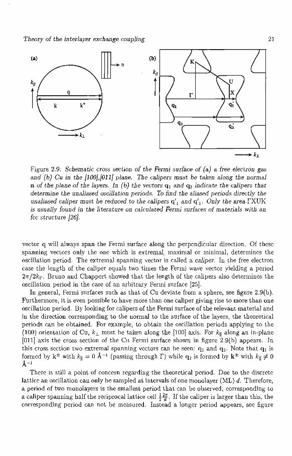
As was just shown, the period of an oscillation is determined by the Fermi wave vector in the case of a free electron gas via >. = 271' /2kF = 271' / qJ.. To illustrate how to obtain the important vector q that determines the period of the oscillation, the spherical Fermi surface of a free electron gas is shown in figure 2.9(a). The coordinates in this figure are kl. on the horizontal axis and k11 on the vertical axis corresponding to the directions perpendicular and parallel to the plane of the film. ql. is the perpendicular component of the vector q indicated in figure 2.9(a) and is equal to the diameter of the Fermi sphere. Given the general equation q = k+ - k - it is clear that q will always span the Fermi surface from (k
11, kJ:) to (kt, k!) . Note that kt = k
11 so that q11 = 0 A- 1 and the spanning
Theory of the interlayer exchange coupling
(a)
illr" (b)
k11
l q
k- k+
-kl
-kl
Figure 2.9: Schematic cross section of the Fermi surface of (a) a free electron gas and (b) Cu in the {100},{011} plane. The calipers must be taken along the normal n of the plane of the layers. In (b) the vectors q 1 and q2 indicate the calipers that determine the unaliased oscillation periods. To find the aliased periods directly the unaliased caliper must be reduced to the calipers q' 1 and q\. Only the area fXUK is usually found in the literature on calculated Fermi surfaces of materials with an fee structure {26}.
21
vector q will always span the Fermi surface along the perpendicular direction. Of these spanning vectors only the one which is extremal, maximal or minimal, determines the oscillation period. The extremal spanning vector is called a caliper. In the free electron case the length of the caliper equals two times the Fermi wave vector yielding a period 211' /2kF. Bruno and Chappert showed that the length of the calipers also determines the oscillation period in the case of an arbitrary Fermi surface [25].
In general, Fermi surfaces such as that of Cu deviate from a sphere, see figure 2.9(b) . Furthermore, it is even possible to have more than one caliper giving rise to more than one oscillation period. By looking for calipers of the Fermi surface of the relevant material and in the direction corresponding to the normal to the surface of the layers, the theoretical periods can be obtained . For example, to obtain the oscillation periods applying to the (100) orientation of Cu, kl. must be taken along the [100] axis. For k11 along an in-plane [Oll] axis the cross section of the Cu Fermi surface shown in figure 2.9(b) appears. In this cross section two extremal spanning vectors can be seen: q 1 and q2 . Note that q 1 is formed by k± with k11 = 0 A-1 (passing through r) while Q2 is formed by k± with k11 i= 0 A-I
There is still a point of concern regarding the theoretical period. Due to the discrete lattice an oscillation can only be sampled at intervals of one monolayer (ML) d. Therefore, a period of two monolayers is the smallest period that can be observed, corresponding to a caliper spanning half the reciprocal lattice cell Pf. If the caliper is larger than this, the corresponding period can not be measured. Instead a longer period appears, see figure

22 Chapter 2
----- I I
;::l 0 I
~ ~ I
I I
4 8 10 12 14 6
spacer thickness (ML)
Figure 2.10: Illustration of the aliasing effect. The solid line represents the unaliased rapid oscillation (period 1.2 ML) which is sampled at integral monolayer thicknesses. A much longer, aliased period of 6.0 ML {6'.0 = I / 2 - 11) appears to be present (dashed line) .
2.10. This period is called the aliased period A and the one corresponding to the caliper the unaliased period .X [27-29]. To obtain the aliased period the following equation is used:
(2.44)
Here, d is the thickness of one monolayer in the relevant direction, that of the surface normal. n is an integer such that ~ :::; j. Therefore the shortest observable period is A = 2d = 2 ML is two monolayers. The equation may be simplified by expressing .X and A in ML, see the caption of figure 2.10. In equation (2.44), the terms on the righthand side correspond to the unaliased caliper and an integral multiple of the width of one Brillouin zone. This indicates that the aliased caliper corresponding to the aliased period can be found by reducing the unaliased caliper until it fits within the first Brillouin zone. In figure 2.9(b), this is demonstrated . By subtracting one reciprocal lattice from the unaliased calipers (<l.l and q2 ) the aliased calipers are identified (q~ and q~) . This is indeed also a caliper, however , of a hole Fermi surface instead of an electron Fermi surface. Note that fX corresponds to 7r/d and that q 1,2 < fX < q' 1,2 • Both q 1 and q 2
would, without aliasing, give rise to a period less than 2 ML which can not be observed . q' 1 gives rise to a rather long period and q' 2 to a relatively short one.
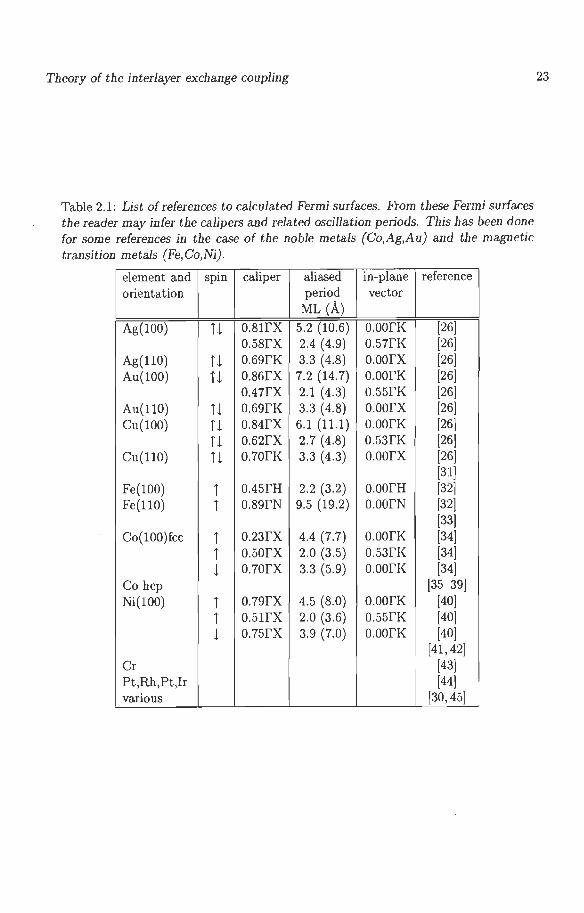
In table 2.1, a list of references to Fermi surfaces published in the literature is given. A few calipers along high symmetry directions and the associated, aliased periods are given. The calipers have been determined by measuring the length of calipers in various directions. In the article of Stiles Fermi surfaces and oscillation periods for a whole range of elements may be found [30] .
Theory of the interlayer exchange coupling
Table 2.1: List ofreferences to calculated Fermi surfaces. From these Fermi surfaces the reader may infer the calipers and related oscillation periods. This has been done for some references in the case of the noble metals (Co,Ag,Au) and the magnetic transition metals (Fe,Co,Ni) .
element and spin caliper aliased in-plane reference orientation period vector
ML (A) Ag(lOO) T! 0.8lrX 5.2 (10.6) o.oorK [26]
0.58rX 2.4 ( 4.9) 0.57rK [26] Ag(llO) i! 0.69rK 3.3 (4.8) o.oorx [26] Au(lOO) i! 0.86rX 7.2 (14.7) o.oorK [26]
0.47rX 2.1 (4.3) 0.55rK [26] Au(llO) i! 0.69rK 3.3 (4.8) o.oorx [26] Cu(lOO) i! 0.84rX 6.1 (11.1) o.oorK [26]
u o.62rx 2.7 (4.8) 0.53rK [26] Cu(llO) T! o.7orK 3.3 (4.3) o.oorx [26]
[31] Fe(lOO) i 0.45rH 2.2 (3.2) o.oorH [32] Fe(llO) i 0.89rN 9.5 (19.2) o.oorN [32]
[33] Co(lOO)fcc i 0.23rX 4.4 (7.7) o.oorK [34]
i o.5orx 2.0 (3.5) 0.53rK [34]
! o.1orx 3.3 (5.9) o.oorK [34] Co hep [35-39] Ni(lOO) i 0.79rX 4.5 (8.0) o.oorK [40]
i o.5lrX 2.0 (3.6) o.55rK [40]
! o.75rx 3.9 (7.0) o.oorK [40] [41, 42]
Cr [43] Pt,Rh,Pt,Ir [44] various [30,45]
23
2.8 Strength, decay and phase
Strength
As noted in section 2.6 the strength of the coupling, the amplitude of the oscillation, is determined by the difference of the reflection coefficients for spin-up and spin-down electrons, see equation (2.43). However, Bruno shows that also the radii of curvature and the group velocities at the extremal points of the Fermi surface play a role [11]. In fact the values of these parameters for the free electron model are already substituted in equation (2.43) E.g. the curvature is of importance in the integration over k11 and E or kJ. in equation (2.38). It determines how much kJ. changes in a region near the extremal points and therefore how much (destructive) interference with neighbouring spanning vectors exists. A strong curvature will lead to a weak coupling.
Decay
In general, the rate of decay depends on the dimensionality of the space (hence also of the reciprocal space with the Fermi volume), the spatial arrangement of the magnetic perturbation (layer, line, point) and the shape of the Fermi surface (sphere, cylinder, cube). In fact the case of a one-dimensional space with a one-dimensional Fermi 'line' with two magnetic point perturbations was already treated in section 2.3. An inverse linear dependence on the distance between the perturbations was found. For layered structures the rate of decay as a function of the spacer thickness usually follows an inverse quadratic law, see equation (2.43). This is the result of the three-dimensional space with a three-dimensional Fermi sphere combined with a two-dimensional in-plane symmetry.
Apart from an intrinsic rate of decay, also external parameters such as growth imperfections within the layers and at interfaces have an effect on the rate of decay. Below interface defects and volume defects are considered.
The influence of defects at the interface depends on the length scale of the defects relative to say the spacer thickness. An example of defects with a large length scale is the roughness at the interfaces of epitaxial multilayers: typically 1 ML steps between terraces of a few 100 A. As long as the roughness at both interfaces of the spacer is not correlated, a distribution of the spacer thickness will result. This, in turn, results in a distribution of the coupling strength. The observed coupling strength as a function of the spacer thickness may be calculated by convoluting the theoretical behaviour with the thickness distribution due to roughness. In general, a reduction of the coupling strength is expected which does not necessarily affect the rate of decay. Already for the minimum roughness of one monolayer the extremely short oscillation periods of sometimes 2 ML are smeared out. To observe a short period oscillation of 2 ML, therefore, requires a constant spacer thicknesses over large areas.
Roughness can also exist on a small length scale. Other interface defects with a small length scale are misfit dislocations. As the effect of the latter is investigated in chapter 5 this topic is discussed in more detail. Bruno and Chappert have dealt with this effect [25]. Misfit dislocations are expected when the lattice parameters of a film aF and a substrate
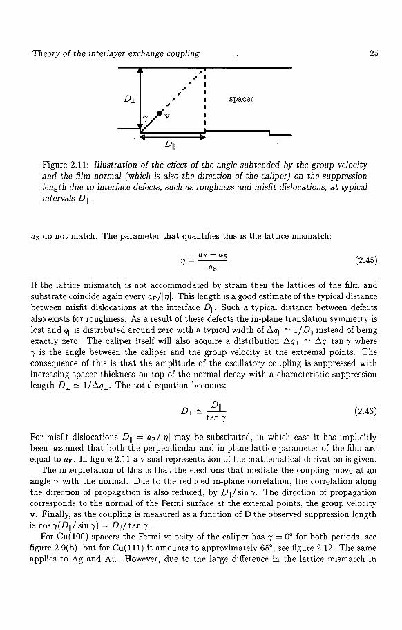
Theory of the interlayer exchange coupling
, , DJ_ , ,
, , I ,
spacer
Figure 2.11: Illustration of the effect of the angle subtended by the group velocity and the film normal (which is also the direction of the caliper) on the suppression length due to interface defects, such a.s roughness and misfit dislocations, at typical intervals D11.
as do not match. The parameter that quantifies this is the lattice mismatch:
25
ap - as 'TJ= (2.45)
If the lattice mismatch is not accommodated by strain then the lattices of the film and substrate coincide again every aF/ l'TJI. This length is a good estimate of the typical distance between misfit dislocations at the interface D11 . Such a typical distance between defects also exists for roughness. As a result of these defects the in-plane translation symmetry is lost and qll is distributed around zero with a typical width of ~qll ::::: 1/ D11 instead of being exactly zero. The caliper itself will also acquire a distribution ~q1- ::::: ~qll tan/ where "'/ is the angle between the caliper and the group velocity at the extremal points. The consequence of this is that the amplitude of the oscillatory coupling is suppressed with increasing spacer thickness on top of the normal decay with a characteristic suppression length D 1- ::::: 1/ ~Q1-· The total equation becomes:
(2.46)
For misfit dislocations D11 = aF/l'TJI may be substituted, in which case it has implicitly been assumed that both the perpendicular and in-plane lattice parameter of the film are equal to ap. In figure 2.11 a visual representation of the mathematical derivation is given.
The interpretation of this is that the electrons that mediate the coupling move at an angle "'/ with the normal. Due to the reduced in-plane correlation, the correlation along the direction of propagation is also reduced, by D11/ sin "Y· The direction of propagation corresponds to the normal of the Fermi surface at the external points, the group velocity v. Finally, as the coupling is measured as a function of D the observed suppression length is cos1(D11/sin1) = D11/tan1.
For Cu(lOO) spacers the Fermi velocity of the caliper has/= 0° for both periods, see figure 2.9(b), but for Cu(lll) it amounts to approximately 65°, see figure 2.12. The same applies to Ag and Au. However, due to the large difference in the lattice mismatch in
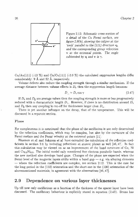
26
x
x
Figure 2.12: Schematic cross section of a detail of the Cu Fermi surface, see figure 2.9(b), showing the caliper at the 'neck' parallel to the (111) direction q 1
and the corresponding group velocities v at the extremal points. The angle subtended by q and v is -y .
Chapter 2
Co/Au(lll) (-13 %) and Co/Cu(lll) (-2.0 %) the calculated suppression lengths differ considerably: 9 A and 52 A, respectively.
Volume defects also reduce the coupling strength through a similar mechanism. If the average distance between volume effects is Dv then the suppression length becomes:
D_1_ ~ Dv COS"( (2.47)
If Dv and Du are average values then the coupling strength is more or less progressively reduced with a characteristic length D _1_. However, if there is no distribution around Dv and Du then any coupling is cut-off for thicknesses larger than D _1_.
There is yet another influence on the decay, that of the temperature. This will be discussed in a separate section.
Phase
For completeness it is mentioned that the phase of the oscillation is not only determined by the reflection coefficients, which may be complex, but also by the curvature of the Fermi surface and the Fermi velocity at the extremal points [11] .
Bloemen et al. and Johnson et al. have extended the calculation of the reflection coefficients in section 2.6 by including reflections at atomic planes as well [46, 47]. In fact this calculation may be viewed on as an improvement of the band structure of Co, Ni and Co0.5Ni0.5 . The initial model only considered free electron parabolic bands, whereas the new method also develops band gaps. Changes of the phase are expected when the Fermi level of the magnetic layers shifts within a band gap - e.g. via alloying elements - where the reflection coefficients are complex, see section 2.12. This is the case for the long period in the (110) orientation and the short one in the (100) orientation of the abovementioned materials, in agreement with the observations [46,47] .
2. 9 Dependence on various layer thicknesses
Up till now only oscillations as a function of the thickness of the spacer layer have been discussed. The oscillatory behaviour is explicitly stated in equation (2.43). Bruno has
Theory of the interlayer exchange coupling 27
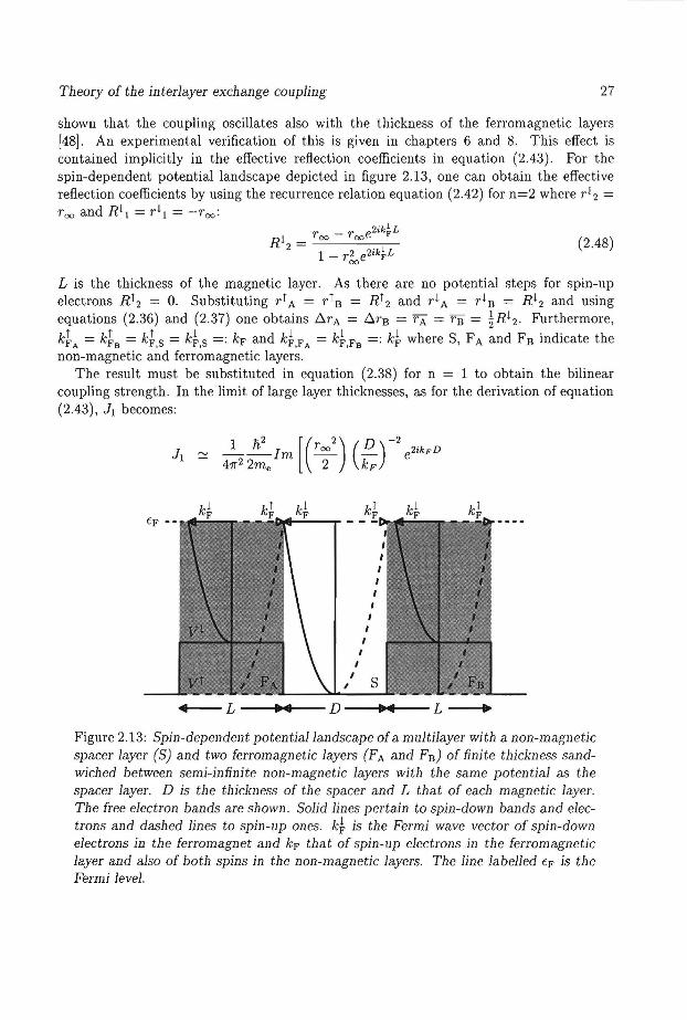
shown that the coupling oscillates also with the thickness of the ferromagnetic layers [48]. An experimental verification of this is given in chapters 6 and 8. This effect is contained implicitly in the effective reflection coefficients in equation (2.43). For the spin-dependent potential landscape depicted in figure 2.13, one can obtain the effective reflection coefficients by using the recurrence relation equation (2.42) for n=2 where r1 2 = roo and R11 = r 11 =-roo:
(2.48)
L is the thickness of the magnetic layer. As there are no potential steps for spin-up electrons RT 2 = 0. Substituting rTA = rTs = RT 2 and r!A = r 1s = R1
2 and using equations (2.36) and (2.37) one obtains !:irA = D.r8 = rA = rs = !R1
2 . Furthermore,
kL = k~8 = k~,s = k~, s =: ky and k~.FA = k~,Fs =: k~ where S, FA and Fs indicate the non-magnetic and ferromagnetic layers.
The result must be substituted in equation (2.38) for n = 1 to obtain the bilinear coupling strength . In the limit of large layer thicknesses, as for the derivation of equation (2.43), J 1 becomes:
Figure 2.13: Spin-dependent potential landscape of a multilayer with a non-magnetic spacer layer (S) and two ferromagnetic layers (FA and F8 ) of finite thickness sandwiched between semi-infinite non-magnetic layers with the same potential as the spacer layer. D is the thickness of the spacer and L that of each magnetic layer. The free electron bands are shown . Solid lines pertain to spin-down bands and electrons and dashed lines to spin-up ones. k~ is the Fermi wave vector of spin-down electrons in the ferromagnet and ky that of spin-up electrons in the ferromagnetic layer and also of both spins in the non-magnetic layers. The line labelled ty is the Fermi level.
28 Chapter 2
(2.49)
This equation shows that apart from an oscillation as a function of the spacer thickness D, also an oscillation as a function of the magnetic layer thickness is expected. In fact, this conclusion is more general. Variation of the thickness of any layer in the whole multilayer stack is expected to give rise to an oscillation of the interlayer coupling strength, e.g. also a cap layer as discussed in chapter 7.
2.10 Fitting oscillatory behaviour
To obtain the oscillation periods from a measured oscillatory behaviour a fit is executed. The fit assumes a phenomenological relation based on equation (2.43) or (2.49) to describe the oscillatory behaviour of the bilinear coupling:
J _ J "'· J0 ,i (27r(t - to,i)) I - 0 + LJ, ( )2 cos A t - to i
(2.50)
The sum runs over the number of observed periods Ai each with its own strength J0 ,i and phase expressed in an offset thickness to,i· If an oscillation as a function of the spacer layer is fitted then J0 = 0 J and t0 = 0 A are used.
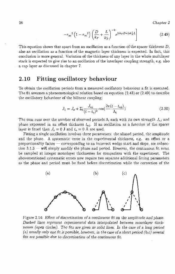
Fitting a single oscillation involves three parameters: the aliased period, the amplitude and the phase. A systematic error in the experimental thickness, e.g. an offset or a proportionality factor - corresponding to an incorrect wedge start and slope, see subsection 3.1.3 - will simply modify the phase and period. However, the continuous fit must be sampled at integer monolayer thicknesses for comparison with the experiment. The abovementioned systematic errors now require two separate additional fitting parameters as the phase and period must be fixed before discretization while the correction of the
(a) (b)
A \ I
Figure 2.14: Effect of discretization of a continuous fit on the amplitude and phase. Dashed lines represent experimental data interpolated between monolayer thicknesses (open circles). The fits are given as solid lines. In the case of a long period (a) usually only one fit is possible, however, in the case of a short period (b,c) several fits are possible due to discretization of the continuous fit.
Theory of the interlayer exchange coupling 29
errors is done afterwards. Nevertheless, the aliased oscillation period of the fit will simply scale with the proportionality factor (for an incorrect wedge slope), even in the case of a short period . However, the amplitude and phase may change dramatically, especially for of a short period. This is illustrated in figure 2.14. Due to errors in the thickness the discretization generally complicates the fitting of an oscillation whereas it does not improve the fit parameters. Therefore, continuous fits will be used to obtain the oscillation periods from experimental data in this thesis. This implies that the amplitudes and phases must be considered with some reserve, especially for the short period .
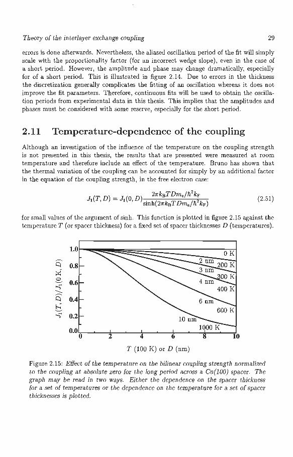
2.11 Temperature-dependence of the coupling
Although an investigation of the influence of the temperature on the coupling strength is not presented in this thesis, the results that are presented were measured at room temperature and therefore include an effect of the temperature. Bruno has shown that the thermal variation of the coupling can be accounted for simply by an additional factor in the equation of the coupling strength, in the free electron case:
(2.51)
for small values of the argument of sinh. This function is plotted in figure 2.15 against the temperature T (or spacer thickness) for a fixed set of spacer thicknesses D (temperatures).
1.0 OK
,--.....
Q 0.8 ;::;::::
e 0.6 ~ -,--..... Q 0.4 b: ~ 0.2 10 nm
0.0 1 00 K 0 2 4 6 8 10
T (100 K) or D (nm)
Figure 2.15: Effect of the temperature on the bilinear coupling strength normalized to the coupling at absolute zero for the long period across a Cu(lOO) spacer. The graph may be read in two ways. Either the dependence on the spacer thickness for a set of temperatures or the dependence on the temperature for a set of spacer thicknesses is plotted.
30 Chapter 2
A reduction of the coupling strength with increasing temperatures is found. Thermal excitations will give rise to a broadening b.q.L of the caliper Q.L which will lead to more destructive interference and hence a weaker coupling. The figure also shows that finite temperatures give rise to an additional decay with spacer thickness on top of the quadratic decay contained in 11 (0, D) . Evaluating this equation in the case of the long period of Cu(lOO) with kF,Cu = 1.471 A- 1 , yields 11 (300 K, 10 A) = 0.9965 11 (0 K, 10 A) and 11(300 K, 40 A)= 0.9461 11(0 K, 40 A) .
For the general case the free electron group velocity nkF/m in the nominator and the argument of sinh must be replaced by the group velocity at the extremal points [11]. This does not affect any of the previous conclusions, except that the rate of decay as a function of interlayer thickness may be different.
2.12 Coupling across insulators and complex Fermi surfaces
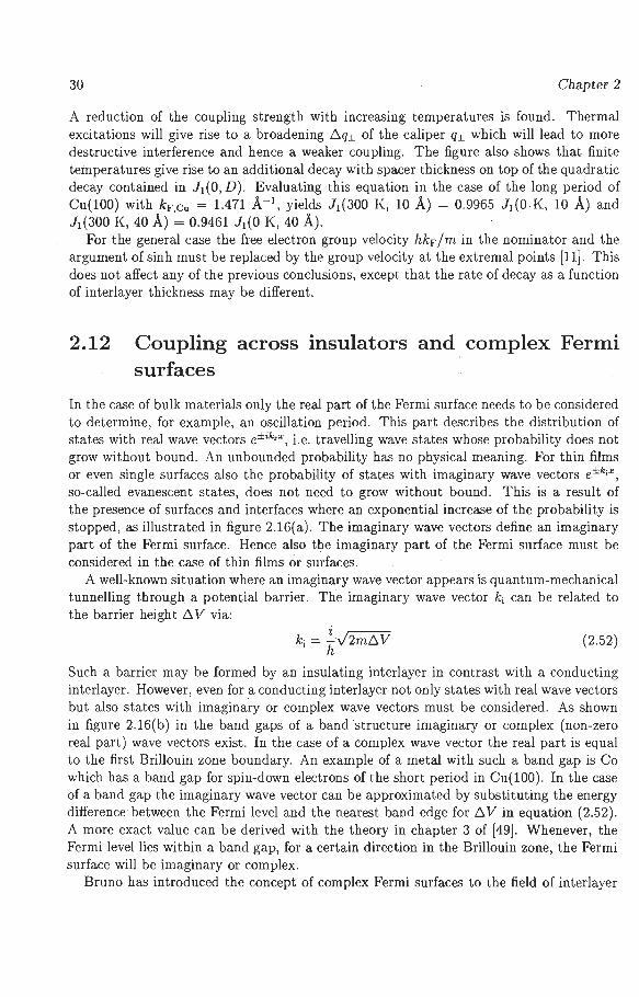
In the case of bulk materials only the real part of the Fermi surface needs to be considered to determine, for example, an oscillation period. This part describes the distribution of states with real wave vectors e±ik,x, i.e . travelling wave states whose probability does not grow without bound. An unbounded probability has no physical meaning. For thin films or even single surfaces also the probability of states with imaginary wave vectors e±k;x,
so-called evanescent states, does not need to grow without bound . This is a result of the presence of surfaces and interfaces where an exponential increase of the probability is stopped , as illustrated in figure 2.16(a) . The imaginary wave vectors define an imaginary part of the Fermi surface. Hence also the imaginary part of the Fermi surface must be considered in the case of thin films or surfaces.
A well-known situation where an imaginary wave vector appears is quantum-mechanical tunnelling through a potential barrier. The imaginary wave vector ki can be related to the barrier height b. V via:
k; = i .J2mb.V ri
(2.52)
Such a barrier may be formed by an insulating interlayer in contrast with a conducting interlayer. However, even for a conducting interlayer not only states with real wave vectors but also states with .imaginary or complex wave vectors must be considered. As shown in figure 2.16(b) in the band gaps of a band structure imaginary or complex (non-zero real part) wave vectors exist. In the case of a complex wave vector the real part is equal to the first Brillouin zone boundary. An example of a metal with such a band gap is Co which has a band gap for spin-down electrons of the short period in Cu(lOO). In the case of a band gap the imaginary wave vector can be approximated by substituting the energy difference between the Fermi level and the nearest band edge for b. V in equation (2.52). A more exact value can be derived with the theory in chapter 3 of [49]. Whenever, the Fermi level lies within a band gap, for a certain direction in the Brillouin zone, the Fermi surface will be imaginary or complex.
Bruno has introduced the concept of complex Fermi surfaces to the field of interlayer
Theory of the interlayer exchange coupling
(a) (b)
, ' , ' , ' , ', imaginary k ,-· '._ ,•' ',
" ' , ' . ~ ' -•" ," _,," ...... ... ........... --- ----
E
real k
0 k
Figure 2.16: (a) Schematic representation of the travelling wave states (solid) and evanescent states (dashed) waves with real and imaginary wave vectors in thin layers or near surfaces. The probability of both states is limited. (b) Real (solid) or imaginary and complex (dashed) wave vectors indicated by arrows in the band structure.
31
exchange coupling in magnetic multilayers. The equations of the coupling strength and its temperature-dependence are valid irrespective of a real or imaginary value of the wave vector in the interlayer. Consequences for the interlayer coupling in the respective cases of real and imaginary wave vectors are: (i) an oscillating versus exponentially decaying coupling strength with increasing thickness of the interlayer, see equation (2.43) , and (ii) a decreasing versus increasing coupling strength with increasing temperature, see equation (2.51). This extension of the Bruno coupling model will be used to describe the results in chapter 9, where a schematic complex Fermi surface will be shown.
2.13 Connection to other models and phenomena
Stiles [30] and Barna.S [50, 51] used a similar approach as Bruno did . Indeed, Barna.S also predicted a dependence on the ferromagnetic layer thickness. However , Bruno has shown that besides the models that used a similar approach also other models are a special case of the Bruno coupling theory [11, 52]. The various models differ in the way the reflection coefficients are calculated and in the order of magnitude of the reflection coefficients.
For example, the pseudo one-dimensional RKKY result of Yafet [21], one of the earliest models , can also be obtained within the Bruno rpodel. Yafet used the three-dimensional range-function of the RKKY theory [17] to calculate the coupling between two monolayers in the limit of large separation . Bruno [11] showed that by using the coefficients of reflection on a delta-function potential barrier, the result of Yafet is obtained if the delta potential is relatively weak.
Another way of looking at interlayer exchange coupling is to consider the spacer layer
32 Chapter 2
as a quantum well. If the poteptial barriers at the interfaces of the spacer are higher than the Fermi level in the well, then the electrons are confined to the spacer, if not then the electrons are partially confined . For a given energy (wavelength) the number of quantum states that fit in the well depends on the width of the well, the thickness of the spacer. As soon as a new quantum state enters the well with increasing thickness the total energy of the system can be lowered by occupying this state. The energy gain must be bargained against the energy cost of confining quantum particles to a finite region.
If one remembers that the orientation of the magnetic moments of the ferromagnetic layers define the height of the barriers, it is dear that the coupling may become alternatingly F and AF. This explanation was given by Mathon and Edwards et al. [53-55]. The case of perfect and partial confinement correspond to reflection coefficients of magnitude lrl = 1 and lrl < 1. The effect on the density of states is also contained in the Bruno model in D.nAB· Taking D.rA = D.r8 = 1 (total confinement in the case of parallel alignment) yields a sawtooth-like function (sharp jump followed by a slow decrease) instead of an oscillation. Each jump corresponds to a new quantum state entering the well.
Finally, Bruno demonstrates how a single-band tight-binding model and the Anderson sd-mixing model fit into his model [11, 56, 57] .
The quantum well states introduced above have been observed using photoemission and inverse photoemission , first without and later with spin polarization analysis [58-61]. The appearance of a quantum well state at the Fermi level coincides with a maximum of the coupling strength , the sign depends on the spin direction of the appearing spin state, as is clearly explained in [61] .
Other properties of multilayers that depend on the presence of such a spin polarized quantum well state at the Fermi level are expected to display oscillations as a function of some layer thickness too. Bennett et al. observed a concurrent oscillation in the interlayer coupling strength and the saturation Kerr effect in Fe/Cu/Fe(lOO) as a function of the Cu thickness [62]. Similar effects were observed for Fe/Au/Fe(lOO), Fe/Ag/Fe(lOO) and Co/Au(lll)/Co as a function of the Au and Ag thickness [63-65] but also as a function of Fe thickness [66]. Apart from oscillations in the saturation Kerr effect also oscillations in the Kerr susceptibility were found [67] . Suzuki and Bruno have presented a theory to explain these effects in terms of an oscillating density of states of (partially) confined electrons [68]. They showed that the oscillation period depends on the wavelength of the light used.
Apart from RKKY oscillations another magnetic oscillatory phenomenon that bears resemblance with the present oscillatory interlayer exchange coupling is the De Haas-Van Alphen (dHvA) effect. The dHvA effect is an oscillation of the magnetic susceptibility as a function of the reciprocal magnetic field strength. Its periodicity is determined by the extremal cross sectional areas of the Fermi surface of the investigated metal, the normal of the extremal areas being parallel to the direction of the applied field. As several extremal areas may exist for specific directions also here a multiperiodicity is observed. Although these features are similar to those of the interlayer coupling, the origin of the dHvA effect is somewhat different. The dHvA effect originates in a shift of quantized orbits of electrons through the Fermi level as a function of the magnetic field. Each time an orbit appears at
Theory of the interlayer exchange coupling 33
the Fermi level the density of states is increased and so is the susceptibility. On the other hand the oscillation of the interlayer coupling is due to quantization of electron states in the potential of the spacer and depends on the thickness of the spacer. Each time a new state enters the potential the coupling strength is maximal F or AF depending on the spin of the state.
2.14 Review of experiments
The chapter is concluded with a review of the experimental results on interlayer exchange coupling obtained so far. Some comment on the tables is given below. For each of the ferromagnetic transition metals Fe and Co a separate table is compiled of the coupling across various spacer materials, tables 2.2 and 2.3. In principle, there is no reason not to investigate the coupling between Ni layers [69]. However, the smaller magnetic moment of Ni, which makes it harder to detect thin films, may have discouraged experimentalists.
In the tables the maximum AF coupling strength, the position of the first maximum, and the period are indicated. The coupling strengths J have been (re )calculated using the following relations:
• bilayers, large anisotropy J = -tµoMsHf
• bilayers, small anisotropy J = -4tµoMsHs
• multilayers, small anisotropy J = -ttµ 0 M 5 H5
Here, t and µ 0 M. are the thickness and saturation magnetization of the magnetic layer, respectively. Hr and H. are the coupling and saturation fields, see section 2.2.
Before general trends are sought, it should be noted that the tables contain results obtained on evaporated (epitaxial) and sputtered samples. The former type of samples usually yields a larger coupling strength due to sharper interfaces and a highly crystalline structure. For the same reasons epitaxial samples sometimes reveal a short period.
The periods typically range from 2 ML '.::::'. 4 A for Co/Cu(lOO) or Fe/Cr(lOO) to 18 A also for Fe/Cr(lOO). Stiles has calculated the oscillation periods for a whole set of elements in various orientations [30]. In the case of the noble metals there is a good agreement. Other 3d, 4d and 5d metals have complicated Fermi surfaces giving rise to a multitude of oscillation periods. Any observed period therefore readily matches one of the predicted periods. Values of the coupling strength range from -0.01 mJ/m2 for Co/Au(lOO) and Fe/Au(lOO) to -5.0 mJ/m2 for Co/Ru(OOOl), in agreement with an estimation from the free electron model in section 2.6.
As a result of different crystal structures and lattice parameters for Fe and Co only a few materials can be deposited in the same orientation and structure - note that Cu grows fee on Co(lOO) but bee on Fe(lOO) . In the few cases where comparison of the periods in both tables is possible, a reasonable agreement is seen: fee Au(lOO) (Co 4 A; Fe 4.1
34 Chapter 2
A), fee Au(lll) (Co 9-15 A; Fe 11 A), fee Cu(lll) (Co 9-17 A; Fe 12 A). Indeed, the period should only depend on the interlayer material and be independent of the magnetic material in this case.
Some spread appears in the corresponding values of the coupling strength , which is more sensitive to the structural quality than the value of the period. Rather the presence or absence of the period is determined by the structural quality. It appears that the coupling strength across Cu is larger than across Au, in the (100) orientation for Fe and both (100) and (111) for Co, however, this can not be explained straightforwardly. The strength depends on the spin asymmetry of the reflection coefficients. In the (100) orientation of Fe this is large due to a band gap for spin-down free electron-like electrons (at k11 = 0) [32] . For Co in the (100) orientation also a band-gap exists for spin-down free electron-like electrons at k11 = 0 giving rise to a similarly large spin asymmetry of the reflection coefficients [34, 40].
An exceptional behaviour was found for Co/Pd and Co/Pt. In these cases the coupling did not oscillate but decreased monotonically with increasing spacer thickness , being always ferromagnetic . This was ascribed to the high polarizability of Pd and Pt. Initially, the study of magnetic multilayers was focused on the perpendicular magnetic anisotropy, discovered in 1985 [3], which is specifically large for Co/Pt and Co/Pd multilayers. In part this explains why the discovery of AF coupling in magnetic multilayers was delayed until 1986 [5] . Later also AF coupling in Fe/Pt [70] and even oscillatory coupling in Fe/Pd were found [71], but still with a F coupling background.
Finally, table 2.4 summarizes the results of coupling studies where the ferromagnetic and cap layer thicknesses are varied. So far these types of experiments have been limited to a few material combinations with an exceptionally small lattice mismatch and high quality epitaxial growth. This is required because multiple interferences extending over more than one layer require extremely sharp interfaces. In addition, all these experiments except the first one made use of wedge-shaped magnetic or cap layers.
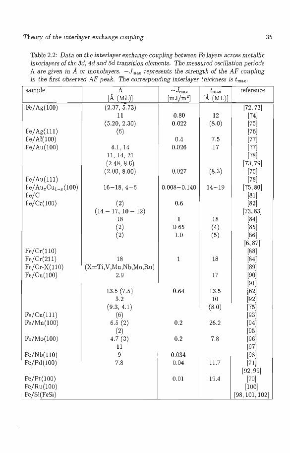
Theory of the interlayer exchange coupling
Table 2.2: Data on the interlayer exchange coupling between Fe layers across metallic interlayers of the 3d, 4d and Sd transition elements. The measured oscillation periods A are given in A or monolayers. -Jmax represents the strength of the AF coupling in the first observed AF peak. The corresponding interlayer thickness is tmax·
sample A -Jmax tmax reference [A (ML)] [mJ/m2
] [A (ML)]
Fe/ Ag(lOO) (2.37, 5. 73) [72, 73] 11 0.80 12 [74]
(5.20, 2.30) 0.022 (8.0) [75] Fe/ Ag(lll) (6) [76] Fe/ Al(lOO) 0.4 7.5 [77] Fe/Au(lOO) 4.1, 14 0.026 17 [77]
11, 14, 21 [78] (2.48, 8.6) [73, 79]
(2.00, 8.00) 0.027 (8.3) [75] Fe/Au(lll) (78] Fe/ AuxCu1-x(lOO) 16-18, 4-6 0.008-0.140 14-19 (75,80] Fe/C [81] Fe/Cr(lOO) (2) 0.6 [82]
(14 - 17, 10 - 12) [73,83] 18 1 18 [84] (2) 0.65 (4) [85] (2) 1.0 (5) [86]
[6,87] Fe/Cr(llO) [88] Fe/Cr(211) 18 1 18 [84] Fe/Cr-X(l 10) (X=Ti,V,Mn,Nb,Mo,Ru) [89] Fe/Cu(lOO) 2.9 17 [90]
[91] 13.5 (7.5) 0.64 13.5 [62]
3.2 10 [92] (9.3, 4.1) (8.0) [75]
Fe/Cu(lll) (6) [93] Fe/Mn(lOO) 6.5 (2) 0.2 26.2 [94]
(2) [95] Fe/Mo(lOO) 4. 7 (3) 0.2 7.8 [96]
11 [97] Fe/Nb(llO) 9 0.034 [98] Fe/Pd(lOO) 7.8 0.04 11.7 [71]
[92, 99] Fe/Pt(lOO) o.oi 19.4 [70] Fe/Ru(lOO) [100]
35
Fe/Si(FeSi) [98, 101, 102]
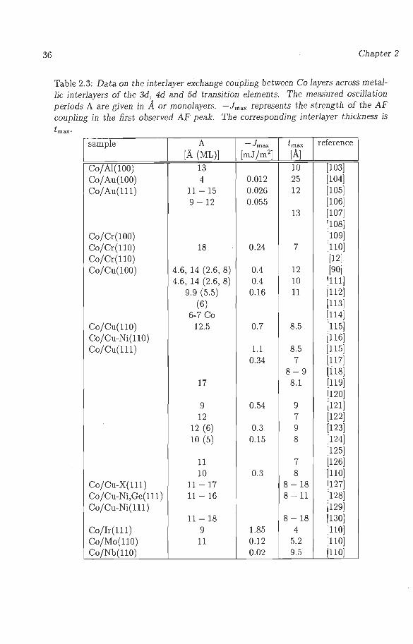
36 Chapter 2
Table 2.3: Data on the interlayer exchange coupling between Co layers across metallic interlayers of the 3d, 4d and 5d transition elements. The measured oscillation periods A are given in A or monolayers. -Jmax represents the strength of the AF coupling in the first observed AF peak. The corresponding interlayer thickness is
imax·
sample A -Jmax imax reference [A (ML)] [mJ/m2
] [A] Co/Al( lOO) 13 10 [103] Co/Au(lOO) 4 0.012 25 [104] Co/Au(lll) 11 -15 0.026 12 [105]
9 - 12 0.055 [106] 13 [107]
[108] Co/Cr(lOO) [109] Co/Cr(llO) 18 0.24 7 [110] Co/Cr(llO) [12] Co/Cu(lOO) 4.6, 14 (2.6, 8) 0.4 12 [90]
4.6, 14 (2.6, 8) 0.4 10 [111] 9.9 (5.5) 0.16 11 [112]
(6) [113] 6-7 Co [114]
Co/Cu( llO) 12.5 0.7 8.5 [115] Co/Cu-Ni(llO) [116] Co/Cu(lll) 1.1 8.5 [115]
0.34 7 [117] 8-9 [118]
17 8.1 [119] [120]
9 0.54 9 [121] 12 7 [122]
12 (6) 0.3 9 [123] 10 (5) 0.15 8 [124]
[125] 11 7 [126] 10 0.3 8 [110]
Co/Cu-X(lll) 11-17 8- 18 [127] Co/Cu-Ni,Ge(lll) 11 - 16 8 - 11 [128] Co/Cu-Ni(lll) [129]
11- 18 8-18 [130] Co/Ir(ll l) 9 1.85 4 [110] Co/Mo(llO) 11 0.12 5.2 [110] Co/Nb(llO) 0.02 9.5 [110]
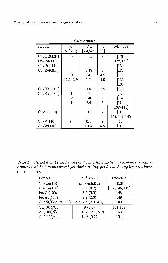
Theory of the interlayer exchange coupling
Co continued
sample A -lmax tmax reference [A (ML)] [mJ/m2
] [A] Co/Os(OOOl) 15 0.55 9 [131] Co/Pd(lll) [132, 133] Co/Pt(lll) [134] Co/Re(OO.l) 0.43 5 [135]
10 0.41 4.2 [110] 10.2, 2.9 0.91 5.0 [136]
[136] Co/Rh(OOOl) 9 1.6 7.9 [110] Co/Ru(OOOl) 11 5 3 [12]
12 0.46 8 [137] 11 5.0 3 [110]
[138-143] Co/Ta(llO) 0.01 7 [110]
[134, 144, 145] Co/V(llO) 9 0.1 9 [12] Co/W(llO) 0.03 5.5 [110]
Table 2.4: Period A of the oscillations of the interlayer exchange coupling strength as a function of the ferromagnetic layer thickness (top part) and the cap layer thickness (bottom part).
I sample A A (ML) reference
Co/Cu(lOO) no oscillation [112] Co/Cu(lOO) 6.5 (3.7) [114, 146, 147] Fe/Cr(lOO) 8.0 (5.5) [148] Fe/Au(lOO) 2.8 (2.0) [149] Co/Ni/Co/Cu(lOO) 3.5, 7.5 (2.0, 4.2) [150]
Cu(lOO)/Co 9 (5.0) [151, 152] Au(lOO)/Fe 5.3, 16.3 (2.6, 8.0) [153] Au(lll)/Co 11.8 (5.0) [154]
37

38 Chapter 2
Chapter 3
Sample preparation and analysis techn.iques
Abstract
To verify the theory on magnetic interlayer coupling the presumed multilayer structures must be made and measured. The experimental techniques to do this are the subject of this chapter. First, the preparation of samples by molecular beam epitaxy and DC magnetron sputtering is discussed. The advantages of using wedge-shaped layers and the demands this makes upon the analysis methods are indicated. Following this, the structural analysis techniques that have been used are mentioned. The magneto-optical measurement method is explained and attention is given to improvements of the magnetic measurement technique.
3.1 Preparation
Deposition of layers onto a substrate lends itself to the purpose of reducing the length scale in one dimension from three-dimensional structures to more two-dimensional layers and films. Existing deposition techniques can be subdivided into three different classes, differing in the way a particle (atom or molecule) flux is generated. One way to do this is by bombardment of a target material by other particles, usually accelerated inert gas ions. In the collision process the excessive energy of the bombarding particles dislodges and ejects target material. Examples are DC (direct current) magnetron sputtering, RF (radiofrequent) sputtering and ion-beam sputtering. Another way is to heat a target material, e.g. by using an electrically heated crucible (Knudsen cell) , an intense electron beam (e-gun) or a pulsed laser beam (laser ablation deposition). As a result the target material starts to evaporate. Finally, material can be deposited from a carrier like a liquid solution (electrodeposition) or a gas (chemical vapour deposition) . The first two classes require a (ultra) high vacuum environment.
In this work only two of these deposition techniques, sputtering (DC magnetron and RF) and evaporation (molecular beam epitaxy), have been used. Currently, these produce sharper interfaces than the other techniques which will bring out the influence of
39
40 Cliapter 3
boundaries more clearly. In the following these two techniques will be discussed in more detail.
3.1.1 Evaporation
In molecular beam epitaxy (MBE) and other evaporation techniques, a beam of material is created by evaporation from a heated source. This evaporated beam then condenses onto a substrate. Epitaxy refers to a well defined relation between the in-plane lattices of the substrate and the deposited film. A match of the in-plane lattice parameter of the film to that of the substrate is often achieved by a contraction or an expansion of the inplane lattice parameter of the film. An opposite deformation of the perpendicular lattice parameter usually accompanies this contraction or expansion. Sometimes a rotation of the film lattice results in a lattice match to the substrate lattice. Therefore, epitaxy is not inherent to the deposition technique, but depends mainly on the combination of materials, although specific growth conditions like substrate temperature are also important.
By using Knudsen cells and e-guns almost all metals can be evaporated. The former have the advantage of stable rates but are only efficient for materials with a high vapour pressure, whereas the latter can evaporate also high melting point materials at the cost of a less stable rate . Deposition rates vary from 0.1 to 1.0 A/s depending on the melting point of the evaporated material and the source temperature. Even during evaporation the ultra high vacuum (pressures in the range 10-8 - 10-9 Pa) is maintained. Typical energies of the condensing atoms are thermal energies of the order 0.1 eV plus any binding energy liberated at the substrate surface. These low arrival energies enable the control over diffusion processes via the substrate temperature to a certain extent. Under optimal conditions MBE can produce multilayers with atomically sharp interfaces. Often, the deposition apparatus is complemented with a large range ofanalysis techniques for (simultaneous) in situ characterization of the growth process. Due to these properties, MBE tends to be more suited for detailed studies relating structural and magnetic properties to details of the growth process. However, it is in general a rather time consuming activity.
The MBE unit at the Philips Research Laboratories Eindhoven (PRLE) is equipped with 3 Knudsen cells and 4 e-guns. Above the sources, the sample is placed on a rotatable, temperature controlled sample stage. The sample temperature can be controlled by heating or cooling the sample stage in the temperature range from ambient temperatures (20 °C) to 700 °C. A study of the homogeneity of the flux at the position of the sample above a Cu Knudsen cell with chemical analysis and scanning Auger electron microscopy (SAM), see subsection 3.2.1, yielded a thickness variation of 10 % to 15 % over 12 mm, a typical sample dimension. Rotation of the substrate during evaporation improves the uniformity of the deposited layer, however, substrate rotation is incompatible with the growing of wedge-shaped layers, see subsection 3.1.3. The sample may be shielded from the flux of each source by the source's -own shutter. Directly in front of the sample stage an additional retractable main shutter, which is used to grow wedges, is placed.
A vibrating quartz crystal is attached to the main shutter to monitor the deposition rate of the sources. The principle of the vibrating crystal technique is that the amount of mass deposited on the crystal changes the vibration frequency of the crystal. All e-
Sample preparation and analysis techniques 41
guns also have an individual crystal facing the source for this purpose. The crystals are regularly calibrated by low angle X-ray diffraction (XRD) analysis of thick homogeneous layers (500 A) or by chemical analysis. In some cases the appearance of reflection high energy electron diffraction (RHEED) oscillations during growth can be used to check the growth rate of the crystals. For sample analysis the MBE is fitted with RHEED, LEED (low energy electron diffraction), SAM, SEM (scanning electron microscopy) and STM (scanning tunneling microscopy). A few of these techniques will be highlighted below. For substrate preparation an annealing and sputtering stage is present. Almost all samples presented here have been produced in this MBE system.
In order not to interrupt the line of thoughts in the presentation of the experimental results, the substrate preparation and the growth conditions for the various experiments are discussed here . Ba.5ically, two types of substrates have been used: disk-shaped Cu single crystals with typical diameters of 12-13 mm and Ge(lOO) 12 x 15 or 4 x 12 rectangles. The Cu crystals were cut from long cylinders with the axis along the (100) , (llO) or (lll) orientation and chemomechanically polished for 8-12 hours in an aqueous mixture of H20 2 and Syton prior insertion into the vacuum. In situ the substrate was treated with several cycles of 1 hour sputtering in an Ar environment and 1 hour annealing at 700 °C until a sharp LEED pattern appeared. During deposition of Co and Ni on these substrates the substrate temperature was 20 °C, to avoid interdiffusion [l13]. When depositing Cu layers or wedges the substrate temperature was raised to 50 °C.
The Ge(lOO) rectangular (15 x 12 mm2 or 12 x 4 mm2 ) substrates were cut from commercially available wafers. After etching in HF they were inserted into the vacuum where they were also sputter-annealed until a sharp LEED pattern appeared . For the Fe/Ge samples the substrate temperature was always 20 °C. For the Fe/Si samples it was also 20 °C except for the first Fe layer and the Si wedge which were deposited at 200 °C. In addition sometimes a sulfur surfactant was used [155] .
3.1.2 DC magnetron and RF sputtering
In DC magnetron sputtering a voltage of typically 1 kV is applied between the target material (cathode) and the anode located near the target. In a low pressure ( 1 Pa) inert gas, usually Ar, the applied voltage difference ignites and maintains a plasma. The ions are accelerated and bombard the target dislodging and ejecting material which then condenses onto a substrate. A complementary flow of electrons is directed towards the anode. On their way the electrons collide with the gas atoms and produce the ionization required to sustain the plasma. A magnetic field from a permanent magnet ring serves to trap the electrons. This enhances the yield of ions and confines the plasma in a region near the target .
Because of the high ion energies (typically 100 eV), almost all metals can be readily sputtered at relatively high deposition rates (1 - 100 A/s). Layers produced with sputtering are highly homogeneous over a lateral range of a few em's up to several dm's, depending on the size of the target. These properties make sputtering a flexible, frequently employed, industrial fabrication technique. On the other hand, the high Ar ion energies cause reflected, neutralized Ar atoms to bombard the substrate, resulting in diffuse inter-
42 Chapter 3
faces and growth defects . Usually, the growth orientation relates to the laterally closed . packed structure: fcc(lll), bcc(llO) and hcp(OO.l) . However, recently, employment of seed layers has established the possibility of epitaxial growth , where the orientation is determined by the substrate and the type of base layer, for sputter deposition of various multilayers [156, 157]. Not only metallic , conducting materials can be sputtered. By applying a radiofrequent voltage, semiconductors and insulators may be sputtered too.
At the PRLE a home made DC magnetron sputtering machine has been used to prepare sputtered samples. It is fitted with three DC sources one of which can by replaced by an RF source. Each source contains a disk-shaped target of 4 cm diameter. Before deposition, the chamber is evacuated to 10-4-10-5 Pa to reduce impurities and vented with Ar (purity 99.98 %) until the pressure reaches 0.9 Pa. The plasmas at all sources are ignited at the start of a run but the particle flux is shielded from a sample plate by individual shutters. The sample plate accommodates ten sample holders which are alternately positioned in front of the relevant sources to deposit multilayers. The distances between the sources and the sample holders equals 7 cm. Each circular sample holder with a diameter of 3 cm may contain several substrates, which measure 4x 12 mm2 . Mostly Si substrates cut from larger wafers were used. Growth rates are 2 - 3 A/s for metals and about 1 A/s for semiconductors. The deposition rates are calibrated by depositing approximately 500 A thick layers in a preceding run, the thickness of which is checked with low angle XRD. Such a calibration procedure of several samples positioned on a single sample holder, showed that the non-uniformity of the particle flux was less than 5 % over 15 mm.
3.1.3 Wedge growth
For systematic studies on layered systems with varying thicknesses, the use of wedgeshaped layers is advantageous provided that a local probe is available. Layers with the shape of a wedge are formed by slowly withdrawing a shutter located between the substrate and source. In this way the deposition time depends linearly on the position thus forming a thickness gradient. Apart from a reduction of substrate and sample preparation time, wedge-shaped layers also guarantee a linear (or at least a monotonous) variation of the thickness and almost identical deposition conditions for the completed sample.
Samples with wedges only constitute a series of separate samples if the local magnetic behaviour is uncorrelated with that at other thickness of the wedge. The magnetic coherence length is of the order of the typical width of domain walls, about 100 A. Hence, separate measurements must at least be spaced 100 A, which condition is clearly satisfied in the present experiments where the spacing is 0.1 mm.
The whole principle of growing wedges stands or falls mainly with the ratio of the mean free path >. and the distance between the source and the substrate dsrc, although the dimensions of the source also play a role. Growing wedges roughly requires >./dsrc > 1. However, a small distance between the shutter and the substrate dshut compared to>. may reduce the lower limit of this inequality. A dshut ~ 0 produces a perfect wedge whatever the value of >.. In a hard spheres approximation the mean free path is given by:
(3.1)
Sample preparation and analysis techniques 43
with n the particle density and r the particle radius. For the low pressures and particle densities in MBE a >. of 105 - 106 m is obtained, which is extremely large compared to a dsrc of 0.3 m. To obtain a constant thickness gradient a homogeneous, stable particle flux and a stable translation velocity of the shutter are required. Furthermore, shadowing due to the finite size of the source is limited if the source diameter is small and dsrc is large compared to dshut, here 2 mm. Minimization of shadowing is particularly important when growing alloy wedges by coevaporation from more than one source. In subsection 3.2.l the determination of the wedge parameters such as slope and starting point is explained.
In principle sputtering at low pressures is also suitable for growing wedges. A rough estimation of>. for a typical pressure of 0.9 Pa using equation (3.1) yields 25 mm , which is of the same order as dsrc = 0.10 m. In this calculation the radius of Argon r = 0.1 nm was used. For a small dshut = 5 mm (as compared to .A) the sputtering of wedges using an eclipsing shutter may still be feasible. A literature search resulted only one experiment with epitaxial, sputtered wedges [158]. During this work the existing sputtering apparatus has been adapted to enable the sputtering of single wedges. Preliminary experiments of interlayer coupling and magnetic anisotropy have indeed demonstrated the presence of a thickness gradient. Optical absorption experiments showed that the gradient is reasonably constant over a large region (20 mm) but deviates at the edges. Typical sample dimensions of sputtered samples with wedges are 4 x 24 mm2. The slope of the wedge is obtained by multiplying the deposition rate and the shutter speed , whereas the offset is aimed to coincide with the sample edge. The combination of the advantages of wedges and the flexibility of sputtering forms a powerful research tool for the quick investigation of the thickness-dependence of various magnetic properties in almost any combination of materials. Although this technique is not optimized yet, it perfectly complements the speed-up of the MOKE measurements discussed in subsection 3.2.3.
3. 2 Analysis
Structural characterization of the evaporated samples is done during growth, because this is extremely complicated if not impossible for the completed samples. As the sputtering apparatus is not equipped with structural analysis techniques one can only rely on the preceding calibration for the composition. This is not the case for samples grown by MBE. Most analysis techniques in the MBE are extremely surface sensitive with penetration depths of only 1 - 10 A. Each layer is therefore characterized after its completion and before the deposition of the following one. For example, structure, wedge parameters and layer thicknesses are determined. To avoid contamination of reactive metal surfaces, and because most techniques require it, this must be done in ultra high vacuum. In addition, all characterization techniques must be compatible with wedge-shaped layers. Thus, only in situ, locally probing characterization techniques are considered.
On the other hand, magnetic characterization of the completed sample can be done ex situ. However , the technique must still be locally probing. In this case contamination can be delayed by covering the completed sample with a thin protective layer of e.g. 20 A Au. This guarantees the sample quality for a few months , enough to allow magnetic characterization. Below the employed analysis techniques that meet the aforementioned
44 Chapter 3
demands are presented.
3.2.1 Scanning Auger microscopy (AES, SAM)
To determine the wedge slope and starting point, Auger electron spectroscopy (AES) with a small probing spot size of 100 µm is used, so-called scanning Auger microscopy (SAM). The element specificity of SAM allows the discrimination between wedge and substrate material. In a positional scan along the wedge, the start of the wedge relative to the edge of the sample is located by finding the onset of an Auger peak associated with the wedge material. By measuring the intensity increase of this peak or the reduction of a peak originating from the substrate material, the slope of the wedge can be obtained. The choice of the Auger peaks is guided by the specific combination of wedge and substrate material , preventing the unwanted interference with peaks of other materials in the sample. For example, to determine the thicknesses of Cu and Co layers the Cu 920 eV and Co 656 eV peaks have been used. Due to the limited penetration depth, or rather escape depth, of the secondary electrons, SAM can be used only for layer thicknesses up to 10 - 20 A. With the deposition rate from calibrated vibrating quartz crystals before and after the wedge deposition and the shutter speed, the wedge slope over the full thickness range can be calculated, i.e. not measured. SAM has the advantage of measuring the values of the actual wedge.
3.2.2 Low energy electron diffraction (LEED)
Low energy electron diffraction (LEED) provides information on the structure of the layers. The perpendicular spacing can be determined by measuring the energies of the primary Bragg reflections along the [00] rod in the energy range 0 - 1000 e V. Parallel lattice spacings are obtained from LEED patterns at fixed electron energy calibrated by the reference LEED pattern of the bulk single crystalline substrate. From these LEED data the crystallinity, the structure and the orientation of the layers can be determined and it can be concluded whether epitaxial growth or lattice relaxation occurred.
3.2.3 Magneto-optical Kerr effect (MOKE)
The magneto-optical Kerr effect was discovered by J. Kerr in 1877 [159]. He noticed that the polarization state of light changes upon reflection from a magnetized surface. There are two effects: Kerr rotation, a rotation of the polarizat ion axis of linearly polarized light and Kerr ellipticity, a change of the ellipticity of the light. Ellipticity is defined as the ratio of the short and long axis of the ellipse described by the electric field vector of the elliptically polarized light. Starting with linearly polarized light, figure 3.1 illustrates the definitions of Kerr rotation and ellipticity.
Phenomenologically the effects of Kerr rotation and ellipticity may be described with complex Fresnel reflection coefficients for left ( - ) and right ( +) circularly polarized light:
R± = r ± exp(i</>±) (3.2)
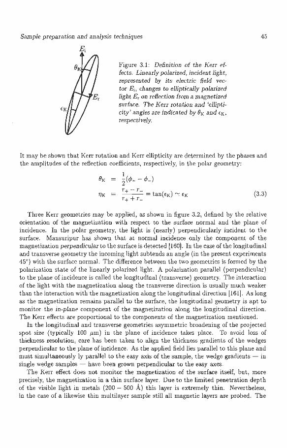
Sample preparation and analysis techniques
£. I
Figure 3.1: Definition of the Kerr effects . Linearly polarized, incident light, represented by its electric field vector Ei , changes to elliptically polarized light E, on reflection from a magnetized surface. The Kerr rotation and 'ellipticity' angles are indicated by BK and fK,
respectively.
45
It may be shown that Kerr rotation and Kerr ellipticity are determined by the phases and the amplitudes of the reflection coefficients, respectively, in the polar geometry:
1 BK = 2(<1>+ - <I>-)
r+ - r_ =tan( tK) ~ tK (3.3) 1]K =
r+ + r_
Three Kerr geometries may be applied , as shown in figure 3.2, defined by the relative orientation of the magnetization with respect to the surface normal and the plane of incidence. In the polar geometry, the light is (nearly) perpendicularly incident to the surface. Mansuripur has shown that at normal incidence only the component of the magnetization perpendicular to the surface is detected [160]. In the case of the longitudinal and transverse geometry the incoming light subtends an angle (in the present experiments 45°) with the surface normal. The difference between the two geometries is formed by the polarization state of the linearly polarized light. A polarization parallel (perpendicular) to the plane of incidence is called the longitudinal (transverse) geometry. The interaction of the light with the magnetization along the transverse direction is usually much weaker than the interaction with the magnetization along the longitudinal direction [161]. As long as the magnetization remains parallel to the surface, the longitudinal geometry is apt to monitor the in-plane component of the magnetization along the longitudinal direction. The Kerr effects are proportional to the components of the magnetization mentioned.
In the longitudinal and transverse geometries asymmetric broadening of the projected spot size (typically 100 µm) in the plane of incidence takes place. To avoid loss of thickness resolution, care has been taken to align the thickness gradients of the wedges perpendicular to the plane of incidence. As the applied field lies parallel to this plane and must simultaneously ly parallel to the easy axis of the sample, the wedge gradients - in single wedge samples - have been grown perpendicular to the easy axes.
The Kerr effect does not monitor the magnetization of the surface itself, but, more precisely, the magnetization in a thin surface layer. Due to the limited penetration depth of the visible light in metals (200 - 500 A) this layer is extremely thin. Nevertheless, in the case of a likewise thin multilayer sample still all magnetic layers are probed. The
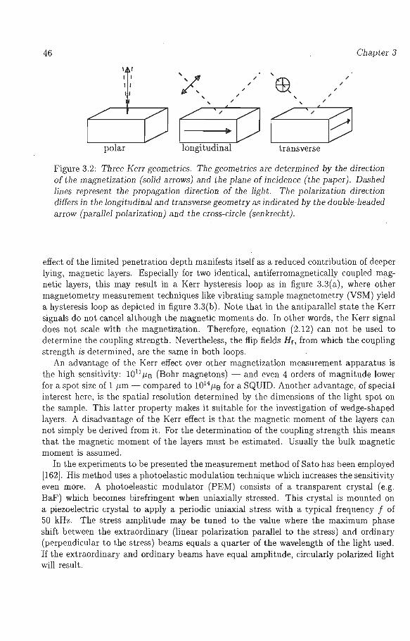
46 Chapter 3
I I
I I x ' " Ea " I I " " " " II " " ' ' ' " ' "
/ " CJ / " ra I I polar longitudinal transverse
Figure 3.2: Three Kerr geometries. The geometries are determined by the direction of the magnetization (solid arrows) and the plane of incidence (the paper). Dashed lines represent the propagation direction of the light. The polarization direction differs in the longitudinal and transverse geometry as indicated by the double-headed arrow (parallel polarization) and the cross-circle (senkrecht).
effect of the limited penetration depth manifests itself as a reduced contribution of deeper lying, magnetic layers. Especially for two identical, antiferromagnetically coupled magnetic layers, this may result in a Kerr hysteresis loop as in figure 3.3(a), where other magnetometry measurement techniques like vibrating sample magnetometry (VSM) yield a hysteresis loop as depicted in figure 3.3(b). Note that in the antiparallel state the Kerr signals do not cancel although the magnetic moments do. In other words, the Kerr signal does not scale with the magnetization . Therefore, equation (2.12) can not be used to determine the coupling strength. Nevertheless, the flip fields Hr, from which the coupling strength is determined, are the same in both loops.
An advantage of the Kerr effect over other magnetization measurement apparatus is the high sensitivity: 1011 µB (Bohr magnetons) - and even 4 orders of magnitude lower for a spot size of 1 µm - compared to 1014 µB for a SQUID. Another advantage, of special interest here, is the spatial resolution determined by the dimensions of the light spot on the sample. This latter property makes it suitable for the investigation of wedge-shaped layers. A disadvantage of the Kerr effect is that the magnetic moment of the layers can not simply be derived from it. For the determination of the coupling strength this means that the magnetic moment of the layers must be estimated. Usually the bulk magnetic moment is assumed.
In the experiments to be presented the measurement method of Sato has been employed [162]. His method uses a photoelastic modulation technique which increases the sensitivity even more. A photoeleastic modulator (PEM) consists of a transparent crystal (e.g. BaF) which becomes birefringent when uniaxially stressed. This crystal is mounted on a piezoelectric crystal to apply a periodic uniaxial stress with a typical frequency f of 50 kHz. The stress amplitude may be tuned to the value where the maximum phase shift between the extraordinary (linear polarization parallel to the stress) and ordinary (perpendicular to the stress) beams equals a quarter of the wavelength of the light used. If the extraordinary and ordinary beams have equal amplitude, circularly polarized light will result.
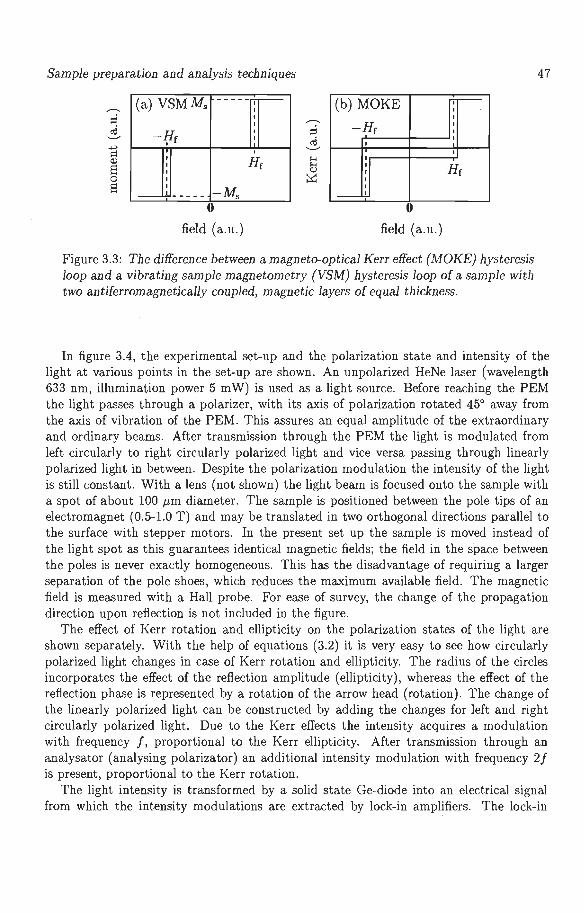
Sample preparation and analysis techniques
(a) VSM Ms -----. -I
(b) MOKE ,,....---I
t I
-;::; <:I)
s 0
I
-ljr I I
' I
Hr I
I
I
-Hr I
I I
I
I I
I
Hr I
I
s I
-Ms - I••---I
_.!,.
0 0
field (a.u.) field (a.u.)
Figure 3.3: The difference between a magneto-optical Kerr effect (MOKE) hysteresis loop and a vibrating sample magnetometry (VSM) hysteresis loop of a sample with two antiferromagnetically coupled, magnetic layers of equal thickness.
47
In figure 3.4, the experimental set-up and the polarization state and intensity of the light at various points in the set-up are shown. An unpolarized HeNe laser (wavelength 633 nm, illumination power 5 mW) is used as a light source. Before reaching the PEM the light passes through a polarizer, with its axis of polarization rotated 45° away from the axis of vibration of the PEM. This assures an equal amplitude of the extraordinary and ordinary beams. After transmission through the PEM the light is modulated from left circularly to right circularly polarized light and vice versa passing through linearly polarized light in between. Despite the polarization modulation the intensity of the light is still constant. With a lens (not shown) the light beam is focused onto the sample with a spot of about 100 µm diameter. The sample is positioned between the pole tips of an electromagnet (0.5-1.0 T) and may be translated in two orthogonal directions parallel to the surface with stepper motors. In the present set up the sample is moved instead of the light spot as this guarantees identical magnetic fields; the field in the space between the poles is never exactly homogeneous. This has the disadvantage of requiring a larger separation of the pole shoes, which reduces the maximum available field. The magnetic field is measured with a Hall probe. For ease of survey, the change of the propagation direction upon reflection is not included in the figure.
The effect of Kerr rotation and ellipticity on the polarization states of the light are shown separately. With the help of equations (3.2) it is very easy to see how circularly polarized light changes in case of Kerr rotation and ellipticity. The radius of the circles incorporates the effect of the reflection amplitude (ellipticity), whereas the effect of the reflection phase is represented by a rotation of the arrow head (rotation). The change of the linearly polarized light can be constructed by adding the changes for left and right circularly polarized light. Due to the Kerr effects the intensity acquires a modulation with frequency f, proportional to the Kerr ellipticity. After transmission through an analysator (analysing polarizator) an additional intensity modulation with frequency 2f is present, proportional to the Kerr rotation .
The light intensity is transformed by a solid state Ge-diode into an electrical signal from which the intensity modulations are extracted by lock-in amplifiers. The lock-in
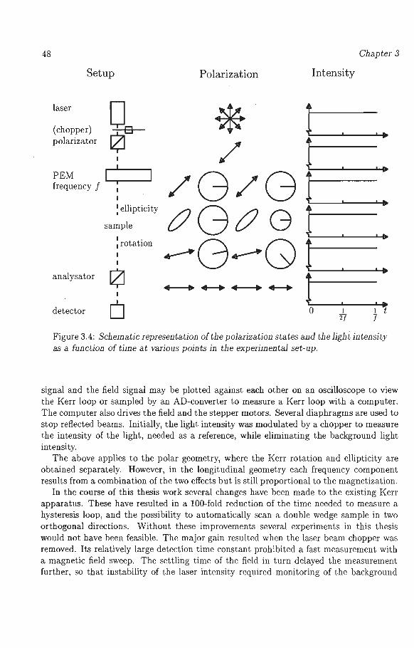
48 Chapter 3
Setup Polarization Intensity
laser 0 * l (chopper) lZJO ... polarizator
/ l I
PEM : /G/G l 1111'
frequency f I ... 1 ellipticity cGc G l I
sample I .
--G--Q l 1111'
1 rotat10n
rZJ ...
analysator
l ... ... ......... ... ............ I
o I 1111'
detector 0 1 I t 2/ 7
Figure 3.4: Schematic representation of the polarization states and the light intensity as a function of time at various points in the experimental set-up.
signal and the field signal may be plotted against each other on an oscilloscope to view the Kerr loop or sampled by an AD-converter to measure a Kerr loop with a computer. The computer also drives the field and the stepper motors. Several diaphragms are used to stop reflected beams. Initially, the light intensity was modulated by a chopper to measure the intensity of the light, needed as a reference, while eliminating the background light intensity.
The above applies to the polar geometry, where the Kerr rotation and ellipticity are obtained separately. However , in the longitudinal geometry each frequency component results from a combination of the two effects but is still proportional to the magnetization.
In the course of this thesis work several changes have been made to the existing Kerr apparatus. These have resulted in a 100-fold reduction of the time needed to measure a hysteresis loop, and the possibility to automatically scan a double wedge sample in two orthogonal directions. Without these improvements several experiments in this thesis would not have been feasible. The major gain resulted when the laser beam chopper was removed. Its relatively large detection time constant prohibited a fast measurement with a magnetic field sweep. The settling time of the field in turn delayed the measurement further, so that instability of the laser intensity required monitoring of the background
Sample preparation and analysis techniques 49
intensity at each field. Thus the problem maintained itself. After removal of the chopper the field could be continuously swept while various loop variables were measured. This took place in such a short time that variation of the laser intensity during the loop measurement was negligible and a simple intensity measurement before and after the loop was sufficient.
50 Chapter 3
Cl1apter 4
Orientational and compositional dependence
Abstract 1
The dependence of the interlayer exchange coupling behaviour, i.e. its oscillation period, strength and phase, on the growth orientation of Co/Cu/Co sandwiches has been investigated. According to coupling models the oscillation periods are determined by extremal spanning vectors (calipers) of the Fermi surface parallel to the growth orientation. An orientational dependence of the number and value of the oscillation periods has been found in agreement with calipers of the Cu Fermi surface in the relevant directions. In addition, a variation of the oscillation period as a result of a slight modification of the Cu Fermi surface, and therefore of the caliper, via alloying with Ni has been observed.
4.1 Introduction and motivation
The discovery that the interlayer exchange coupling strength oscillates as a function of the non-magnetic interlayer thickness in a wide variety of magnetic multilayers [62, 110, 123, 124], has presented a considerable challenge to solid state physicists. Early experiments suggested rather an indifference of the oscillation period to the interlayer material as the observed oscillation periods all fitted in the range 9 - 11 A, although Cr formed an exception with a period of 18 A [110]. The overall period of 9 - 11 A may have been a result of the presence of interface roughness in sputtered samples obscuring much shorter periods. Indeed MBE-grown epitaxial sandwiches with sharp interfaces displayed a variety of oscillation periods, ranging from 2 ML (::::::: 4 A), the detectable minimum, up to 20 A, see e.g. [77, 82, 83, 94].
As explained in chapter 2, theorists ascribed these oscillation periods to interference of travelling waves in the interlayer that are reflected spin-dependently at the interfaces
1 Parts of this chapter have been published in Phys. Rev Lett. 69, 969 (1992) and in Mat. Res. Soc. Symp. Proc. 313, 93 (1993).
51
52 Chapter 4
with the ferromagnetic layers. The periods of the oscillations are obtained from extremal spanning vectors of the Fermi surface parallel to the growth orientation (calipers) . In addition, one must take into account the discrete sampling at integer thicknesses of the interlayer, the so-called aliasing effect. On the basis of this aliasing effect alone a dependence of the oscillation period on the growth orientation is already expected as the thickness of a monolayer depends on the growth orientation . This is true even for a free electron gas with a spherical Fermi surface.
An additional argument for the orientational dependence of the oscillation periods exists for interlayers with a non-spherical Fermi surface. In that case the length of a caliper itself will also depend on the growth orientation. Bruno and Chappert derived the calipers q, which generate oscillation periods equal to 2?r/lqJ.I , of the noble metal (Cu, Ag and Au) Fermi surfaces for three growth orientations: (100), (llO) and (111) [163]. In this way, a multiplicity of oscillation periods was obtained, the number and values of which are predicted to depend upon the growth direction of the samples. Strong support of this Fermi surface picture has been supplied by coupling investigations on Co/Cu(lOO) [90], Fe/ Au(lOO) [77) and Fe/ Ag(lOO) [72] samples, where a superposition of oscillations with periods close to those predicted in [163] was established.
The relatively simple nature of the Cu Fermi surface makes this a suitable candidate for the verification of the various aspects of interlayer exchange coupling theories, such as the orientational dependence. In addition, the discovery of sizable antiferromagnetic (AF) coupling and giant magnetoresistance effects in sputtered, (111) oriented Co/Cu [123, 124) and Fe/Cu [93] multilayers is of great interest to theorists and applications engineers alike. In an attempt to enhance these effects, Egelhoff and Kief have used MBE instead of sputtering to grow a number of Co/Cu(lll) and Fe/Cu(lll) samples on single crystalline Cu(lll) substrates [125]. However , in contrast to the situation in the sputtered samples, these supposedly high quality, MBE-prepared samples not only failed to give an enhanced AF coupling, but actually displayed no AF coupling at all.
To explain this anomaly, it has been proposed that the AF coupling in (111) oriented , sputtered samples is attributable to a minority presence in the samples of (100) crystallites [125) - to which a certain credence is lent by the samples' relatively broad rocking curves. However, in the light of results on epitaxial MBE-grown (100) Co/Cu/Co, this proposal becomes fraught with problems [90] . Firstly, no detectable fraction of (100) oriented crystallites has been observed by either X-ray diffraction or electron diffraction in strongly AF coupled, (111) textured, sputtered samples [164]. Secondly, the coupling-oscillations in the two systems show different periods and phases. Finally, the AF coupling strength in the MBE-grown Co/Cu(lOO) sample is lower than that observed in some sputtered (lll) Co/Cu/Co samples, whereas a minority component is required to exhibit a proportionally greater coupling strength to compensate for its reduced abundance. This controversy also motivated an investigation of the interlayer coupling in Co/Cu/Co sandwiches with (100), (ilO) , and (111) orientations, the results of which will be presented in the next sections.

Orientational and compositional dependence 53
4.2 Experimental
To study the orientational dependence, single crystalline Cu substrates with three different orientations have been used, in combination with wedge-shaped Cu interlayers. The precise composition of the completed samples is given in table 4.1.
The AF coupling strengths J have been determined from analysis of longitudinal Kerr hysteresis loops measured at room temperature along the wedges, i.e. as a function of Cu thickness. The external magnetic field was applied along the [110] (in-plane easy) axis for the (100) sample, the [111] (easy) axis for the (110) sample, and in an arbitrary direction (no in-plane anisotropy) for the (111) sample.
Table 4.1: Overview of the thicknesses of the layers in the Co/Cu wedge/Co sandwiches used in the study of the orientational dependence. The wedge slopes were typically 4 A/mm.
substrate magnetic interlayer magnetic cap layers underlayer wedge overlayer
(A) (A) (A) (A) Cu(lOO) 60 Co 0- 40 Cu 60 Co 7Cu + 20 Au Cu(llO) 40 Co 0 - 44 Cu 40 Co 7 Cu+ 20 Au Cu(110) 40 Co 0 - 40 Cu90Ni10 40 Co 10 Cu+ 20 Au Cu(111) 40 Co 0 - 35 Cu 40 Co 7 Cu+ 20 Au
4.3 Results and discussion
As a result of the identical lattice mismatch of -2.0 % and the same fee structure in all three orientations, the growth of the samples showed similar characteristics for all three orientations. Across the entire sample, the Cu wedges displayed identical lattice constants to those of the Cu single crystalline substrates, and maintained an fee structure, see the LEED patterns in figure 4.1. The Co layers displayed a fee surface lattice nearly identical to that of the Cu substrate, i.e. the Co grows epitaxially. As the lattice parameter of Cu is larger than that of Co, the Co lattice is expanded in the plane of the film. This in-plane expansion is accompanied by a minimal contraction of the perpendicular lattice constant of Co, resulting in slightly tetragonally deformed Co. LEED-IV measurements yielded a perpendicular Co-Co spacing of 1.70 A, 1.23 A and 2.02 A for the (100), (110) and (111) orientations, respectively. These are slightly less than the corresponding perpendicular Cu-Cu spacings of 1.80 A, 1.27 A and 2.09 A. The error in these values is estimated to be 0.02 A.
For the (110) sample, a certain amount of streaking occurred in the LEED patterns upon deposition of Co on the Cu substrate, being particularly obvious in the [100] directions, where the surface is most open. Further evaporation of Cu reduced the width of these streaks considerably, with subsequent Co evaporation resulting in the reappearance
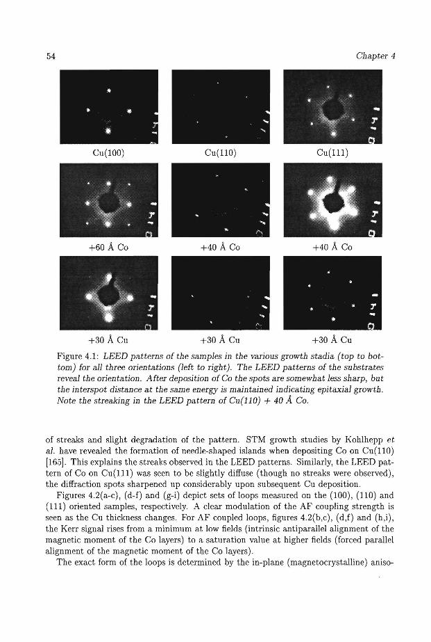
54 Chapter 4
Cu(lOO) Cu(llO) Cu(lll)
+60 A Co +40 A Co +40 A Co
+30 A Cu +30 A Cu +30 A Cu
Figure 4.1: LEED patterns of the samples in the various growth stadia (top to bottom) for all three orientations (left to right). The LEED patterns of the substrates reveal the orientation. After deposition of Co the spots are somewhat less sharp, but the interspot distance at the same energy is maintained indicating epitaxial growth. Note the streaking in the LEED pattern of Cu(llO) + 40 A Co.
of streaks and slight degradation of the pattern. STM growth studies by Kohlhepp et al. have revealed the formation of needle-shaped islands when depositing Co on Cu(llO) [165]. This explains the streaks observed in the LEED patterns. Similarly, the LEED pattern of Co on Cu(lll) was seen to be slightly diffuse (though no streaks were observed), the diffraction spots sharpened up considerably upon subsequent Cu deposition.
Figures 4.2(a-c), (d-f) and (g-i) depict sets of loops measured on the (100), (110) and (111) oriented samples, respectively. A clear modulation of the AF coupling strength is seen as the Cu thickness changes. For AF coupled loops, figures 4.2(b,c) , ( d,f) and (h,i), the Kerr signal rises from a minimum at low fields (intrinsic antiparallel alignment of the magnetic moment of the Co layers) to a saturation value at higher fields (forced parallel alignment of the magnetic moment of the Co layers) .
The exact form of the loops is determined by the in-plane (magnetocrystalline) aniso-

Orientational and compositional dependence
(a) ( 100) Jo'g.oooooooooc
9.7 A Cu
-50 0 50 -200 0
(g) (111) 0 o._o0o"o .. oJ:to0.0•00!
3.3 A CuJ
0
0 I
o.0000·00·0"000°1° 200 -50 0 50
(b) (100) ~-~'"((.((((f((((
oc; •0
( e) ( 110 ,,,,,10,o~~"o<<ccro (h) (111) 9.8 A Cu 11.8 A Cu r.1
oO ·• _.,o :-.-.~,,(~\_c.Ol
~""~"l"'~ Hr 00
0
13.o A Cu
0
P.' oll •O .,. <lrl<<<'"'-''""o' <c(Oc.Cic<Occ.CC',cOlO
-100 0 100 -50 0
( C) ( lOO) ~ o;roooooc1c
21.3 A Cu J: / I :,o
01-----oot.11'>c)o0-----i il( Hr
o~ooooo:oi> -50 0 50 -50
field (kA/m)
50 -300
(i) (111) 22.6 A
0 Cu
50 -100
0 300
Hs
0 100
Figure 4.2: MOKE hysteresis loops for MBE-grown (100) (a-c), (110) (d-f) and (111) (g-i) Co/Cu/Co. The Cu thickness is given in each individual case.
55
tropy of the Co layers. Although the shape of the loops already reveals that the anisotropy plays an important role in the (100) and (110) orientations, an independent measurement of the anisotropy can confirm this. By applying the field along the in-plane hard axis at a position of ferromagnetic coupling, e.g. 15 A Cu for the (110) sample, an anisotropy loop can be measured. The saturation field of such a loop is proportional to the magnetic anisotropy constant. In this way a typical value K(lrn) = 0.4 MJ /m3 has been found. K(loo) is expected to have a similar value. Given the maximum AF coupling strengths J below and the magnetic layers thicknesses t, it can be verified that K(loo)/(IIO)t > -J. Therefore, the resulting loops in the (100) and the (110) case are indeed expected to resemble the theoretical loops in figure 2.3(b,c). As a result of the limited anisotropy, the magnetic moments may rotate slightly at low fields until a relatively sharp transition to parallel alignment at the flip field Hr, see figure 4.2(b,d). The separation of the two branches of the loops around zero field can be a result of slightly unequal layer thicknesses
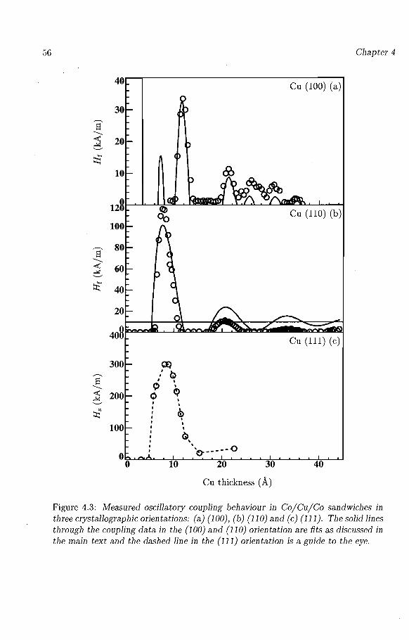
56
40
30
s --....... -< 20 ..;.:: '--'
~ 10
128
100
s 80 --....... -< 60 ..;.:: '--'
~ 40
20
408
300
s --....... -< 200 ..;.:: .__,
::6" 100
a) ,' Q ' ' ~ '
0 ~ ' I I
I
0 ' I '
10 20 30
Cu thickness (A)
Chapter 4
Cu (100) (a)
Cu (110) (b)
Cu (111) (c)
40
Figure 4.3: Measured oscillatory coupling behaviour in Co/Cu/Co sandwiches in three crystallographic orientations: (a) (100), (b) (110) and (c) (111). The solid lines through the coupling data in the (100) and (110) orientation are fits as discussed in the main text and the dashed line in the (111) orientation is a guide to the eye.
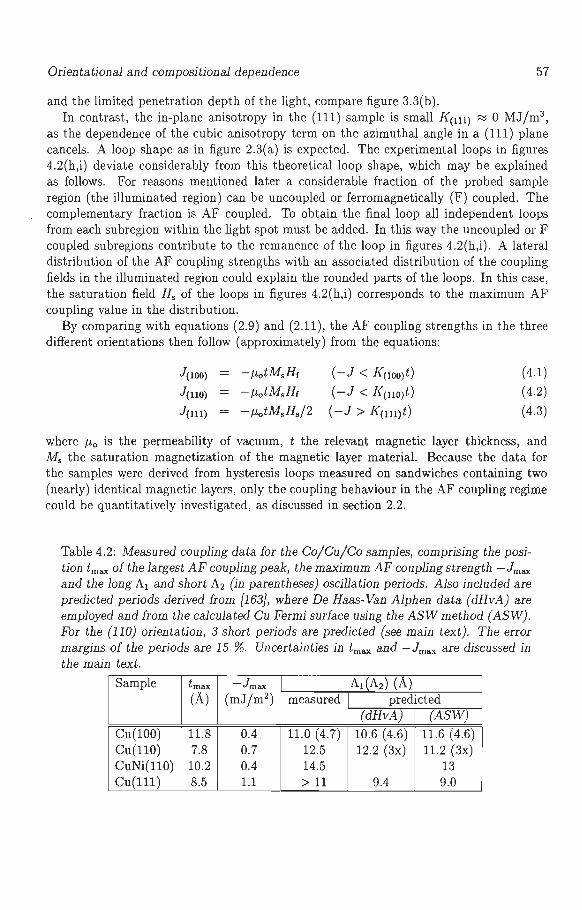
Orientational and compositional dependence 57
and the limited penetration depth of the light, compare figure 3.3(b ). In contrast, the in-plane anisotropy in the (111) sample is small !{(1 11 ) ::::::: 0 MJ/m3,
as the dependence of the cubic anisotropy term on the azimuthal angle in a (111) plane cancels. A loop shape as in figure 2.3(a) is expected. The experimental loops in figures 4.2(h,i) deviate considerably from this theoretical loop shape, which may be explained as follows. For reasons mentioned later a considerable fraction of the probed sample region (the illuminated region) can be uncoupled or ferromagnetically (F) coupled. The complementary fraction is AF coupled. To obtain the final loop all independent loops from each subregion within the light spot must be added. In this way the uncoupled or F coupled subregions contribute to the remanence of the loop in figures 4.2(h,i). A lateral distribution of the AF coupling strengths with an associated distribution of the coupling fields in the illuminated region could explain the rounded parts of the loops. In this case, the saturation field H. of the loops in figures 4.2(h,i) corresponds to the maximum AF coupling value in the distribution.
By comparing with equations (2.9) and (2.11), the AF coupling strengths in the three different orientations then follow (approximately) from the equations:
J(loo)
}(110)
1(111)
-µ0 tM.Hr
-µ0 tM.Hr
-µ0 tM.H./2
(-J < I<(loo)t)
(-J < I<(110)t)
(-J > I<(11l)t)
(4.1)
( 4.2)
(4.3)
where µ0 is the permeability of vacuum, t the relevant magnetic layer thickness, and Ms the saturation magnetization of the magnetic layer material. Because the data for the samples were derived from hysteresis loops measured on sandwiches containing two (nearly) identical magnetic layers, only the coupling behaviour in the AF coupling regime could be quantitatively investigated, as discussed in section 2.2.
Table 4.2: Measured coupling data for the Co/Cu/Co samples, comprising the position tmax of the largest AF coupling peak, the maximum AF coupling strength -lma.x
and the long A1 and short A2 (in parentheses) oscillation periods. Also included are predicted periods derived from {163}, where De Haas-Van Alphen data (dHvA) are employed and from the calculated Cu Fermi surface using the ASW method (ASW). For the (110) orientation, 3 short periods are predicted (see main text). The error margins of the periods are 15 %. Uncertainties in tma.x and -lma.x are discussed in the main text.
Sample lma.x -Jma.x A1(A2) (A) (A) (mJ/m2) measured predicted
(dHvA) (ASW)
Cu(lOO) 11.8 0.4 . 11.0 (4.7) 10.6 (4.6) 11.6 ( 4.6) Cu(llO) 7.8 0.7 12.5 12.2 (3x) 11.2 (3x) CuNi(llO) 10.2 0.4 14.5 13 Cu(111) 8.5 1.1 > 11 9.4 9.0
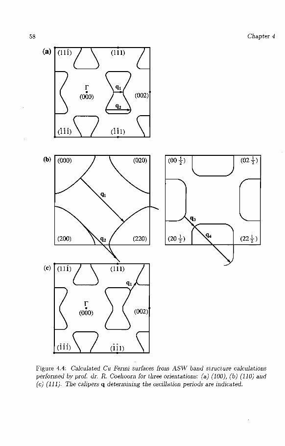
58 Chapter 4
(a) (11 i) (111)
r •
(000) (002)
(iii) (ii 1)
(b) (000) (00 t> (02t)
(200) (220) (20 +> (22+)
(c) (11 i)
r •
(000)
(iii) (111)
Figure 4.4: Calculated Cu Fermi surfaces from ASW band structure calculations performed by prof. dr. R. Coehoorn for three orientations: (a) (100), (b) (110) and (c) (111). The calipers q determining the oscillation periods are indicated.
Orientational and compositional dependence 59
In figure 4.3 the flip fields or the saturation fields are plotted against the Cu spacer thickness for all three orientations. Using equations ( 4.1 ), ( 4.2) and ( 4.3) the AF interlayer exchange coupling strength may be calculated for non-zero fields. A clear but different oscillation is observed for the (100) and (110) orientations. For the (111) orientation only a single AF coupling peak is found from which the oscillation period can not be obtained.
Before discussing each orientation in detail below, the experimental results (oscillation period, strength and position of the first AF coupling peak) are compiled in table 4.2. In addition to uncertainties in positioning on the sample and in the fits of the results, uncertainties in the the start (0.2 mm) and slope (15 %) of the wedge add to the total error margin of the phases. Only the uncertainties in the wedge slope and in the fits determine the error margin of the periods. The table also contains predicted periods of the oscillatory exchange coupling across Cu spacers for all three orientations. These theoretical periods were' obtained from De Haas-Van Alphen data given by Bruno and Chappert in reference [163] and from augmented spherical wave (ASW) band structure calculations1 . In figure 4.4 the cross sections of the Fermi surface obtained from the ASW calculations are shown and the calipers are indicated.
(100) Orientation
Figure 4.3(a) depicts the thickness-dependence of the oscillatory AF ~oupling in the Cu(lOO) sample, with 5 AF coupling peaks clearly visible. A fit of the experimental coupling data for this sample was attempted using a superposition of a short (A1) and long period (A2) oscillation as suggested by the two extremal vectors q in figure 4.4(a). Equation (2.50) with }0 = 0 J and t0 = 0 A and two periods has been used. The fit plotted in figure 4.3(a) as a solid line, was obtained for the following parameter values: (A1 , to, 1 , lo,1) = (11.0 A, 11.5 A, -22 10-23 J) and (A2 , to,2 , lo,2) = (4.7 A, 11.8 A, -26 10-23 J). Generally, there is good agreement between the fit and the experimental peak positions, however, the peak heights do not agree as well. In relation with the remarks made in section 2.10 this may be expected.
The fit already deteriorates considerably with a small variation of 0.2 A of the short period, while for the long period variations of 1 A or more start to impair the fit. These values indicate the uncertainty in the fitted period. From De Haas-Van Alphen data on the Fermi surface of Cu, Bruno and Chappert have predicted periods of 4.6 A and 10.6 A. The calipers q which follow from the Cu Fermi surface calculated with the ASW method, lead to periods of 4.6 and 11.6 A. The values of the experimental periods match well with the predicted ones, see table 4.2.
It is expected that the amplitude of the short period is larger than that of the long period due to a band gap (perfect confinement and reflection) in Co for the spin-down electrons of the short period in Cu [166]. The fit parameters confirm this. In addition, noting that the strength of the short period is more sensitive to roughness and defects, this is even more so. The maximum AF coupling strength is lma.x,(IOO) = -0.4 mJ/m2
. This value, as determined from the Kerr loops is very accurate, however, it strongly depends on the sample quality (roughness, defects, strain, purity) which is difficult to quantify.
1The ASW calculations have been performed by prof. dr. R. Coehoorn.
60 Chapter 4
Therefore this value must be considered as a lower limit when comparing it with other results or theory.
(110) Orientation, compositional dependence
The (110) oriented Co/Cu sandwich displayed only one oscillation period. Therefore a fit on the basis of equation (2.50), but with only one period and J0 = 0 J and t0 = 0 A, was attempted and resulted the solid line in figure 4.3(b). In this case the fit parameters are: (A1, t0 ,1, J0 ,1) = (12.5 A, 8.6 A, -43 10-23 J). Here, the value of the long period is much more fixed in order to obtain a good fit (±0.5 A). As it is, not all peak heights could be fitted correctly, however, a downward shift of 1.2 A in the thicknesses yielded perfect agreement. Given a wedge slope of 4 A/mm this shift corresponds to a combined positioning error and wedge start error of only 0.3 mm which is rather realistic.
The value of 12.5 A agrees well with the theoretical period following from the neck diameter of the Cu Fermi surface, vector q3 in figure 4.4(b ). Additional shorter periods of 2.7, 3.2 and 4.2 A are predicted to appear, but these were not found in the first sample that was investigated [163]. A second sandwich, with a shallower Cu wedge, was therefore prepared and carefully scanned, but this too failed to reveal any evidence of additional shorter period oscillations. Extremely flat coherent interfaces would be required to detect such periods. This may be hampered by the formation of needle-shaped islands as witnessed in STM studies [165].
The maximum coupling field at 7.8 A Cu yields an AF coupling strength lmax,(llO) = -0.7 mJ /m2 . This coupling value has been determined via a minimum energy analysis, using the experimental value of the anisotropy constant Kcuo), as done for the (100) orientation in figure 2.4.
Because only one of its predicted periods is easily observable, the (110) orientation lends itself ideally to experimental examination of the period variation predicted to arise from compositional modification of the Cu interlayer. The principle of this period variation can be understood by considering a free electron gas with a parabolic band and a spherical Fermi surface. In this case the caliper, which determines the oscillation period, equals the diameter of the Fermi sphere or two times the Fermi wave vector. The relation between the Fermi energy and the Fermi wave vector is expressed by the parabolic band. Addition or reduction of the number of electrons will fill or empty states near the Fermi level and thereby raise or lower the Fermi level. The associated variation of the Fermi wave vector will directly yield a variation of the oscillation period. Such a variation of the number of electrons can be achieved by alloying the spacer material with other elements with a different valence.
A particularly suitable candidate for alloying with the Cu spacer is Ni (one electron less than Cu). CuNi alloys readily form solid solutions displaying fee structures and lattice constants which, for limited Ni concentrations, are extremely well matched to Co [167]. It should be noted that these alloys are not ferromagnetic for atomic concentrations of Ni in Cu below 40 % [168, 169]. When Ni is alloyed with Cu, the number of electrons decreases and the electron Fermi surface contracts. The contraction shortens the caliper q3 , see figure 4 .4 (b), and directly leads to an expansion of the associated long period of
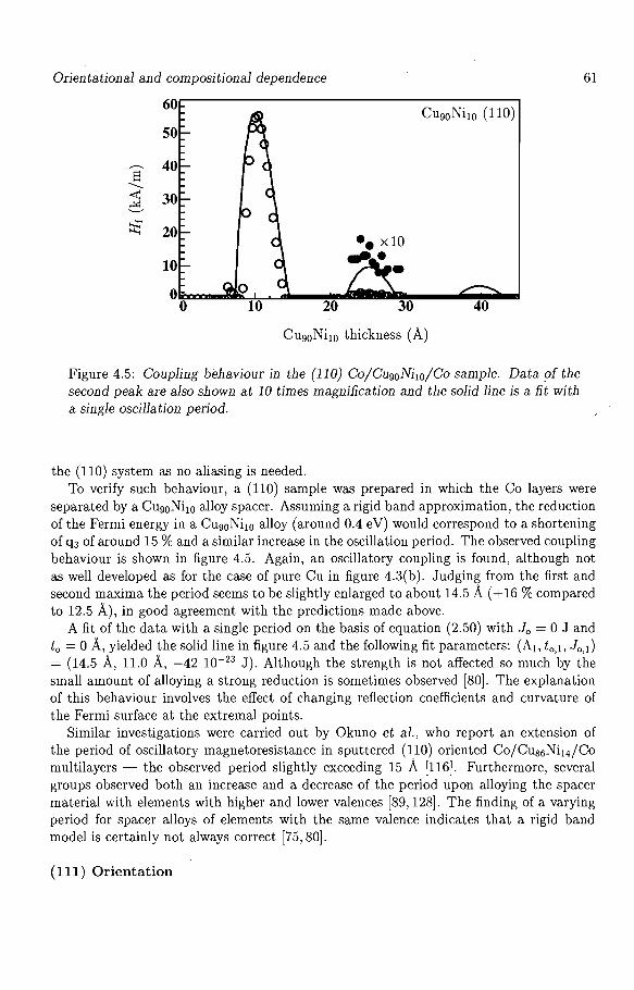
Orientational and compositional dependence
Cu90Ni10 (110)
20 40
Cu90Ni10 thickness (A)
Figure 4.5: Coupling behaviour in the (110) Co/Cu90 Ni10/Co sample. Data of the second peak are also shown at 10 times magnification and the solid line is a fit with a single oscillation period.
the (110) system as no aliasing is needed.
61
To verify such behaviour, a (110) sample was prepared in which the Co layers were separated by a Cu90 Ni10 alloy spacer. Assuming a rigid band approximation, the reduction of the Fermi energy in a Cu90 Ni10 alloy (around 0.4 eV) would correspond to a shortening of q 3 of around 15 % and a similar increase in the oscillation period. The observed coupling behaviour is shown in figure 4.5. Again, an oscillatory coupling is found, although not as well developed as for the case of pure Cu in figure 4.3(b). Judging from the first and second maxima the period seems to be slightly enlarged to about 14.5 A ( + 16 % compared to 12.5 A), in good agreement with the predictions made above.
A fit of the data with a single period on the basis of equation (2.50) with 10 = 0 J and t0 = 0 A, yielded the solid line in figure 4.5 and the following fit parameters: (A1, t 0 , 1 , 10 , 1 )
= (14.5 A, 11.0 A, -42 10-23 J). Although the strength is not affected so much by the small amount of alloying a strong reduction is sometimes observed [80]. The explanation of this behaviour involves the effect of changing reflection coefficients and curvature of the Fermi surface at the extremal points.
Similar investigations were carried out by Okuno et al., who report an extension of the period of oscillatory magnetoresistance in sputtered (110) oriented Co/Cu86Ni14 /Co multilayers - the observed period slightly exceeding 15 A [116]. Furthermore, several groups observed both an increase and a decrease of the period upon alloying the spacer material with elements with higher and lower valences [89, 128]. The finding of a varying period for spacer alloys of elements with the same valence indicates that a rigid band model is certainly not always correct [75, 80].
( 111) Orientation
62 Chapter 4
Initially, the absence of AF coupling in MEE-prepared (111) Co/Cu multilayers has been reported. It has been proposed that the oscillatory coupling observed in sputtered (111) textured Co/Cu multilayers might be attributable to the presence of minority components of a different crystallographic orientation [125]. In this light, an attempt has been made to detect intrinsic coupling in an MBE-grown (111) Co/Cu wedge/Co sandwich.
The observed coupling behaviour for this sample is shown in figure 4.3(c) . A strong AF coupling peak occurs at 8.5 A, with weak indications of a second peak at about 20 A suggesting an oscillation period of at least 11 A. The saturation field in the primary peak corresponds to an AF coupling strength lmax,(lll) ~ -1.1 mJ/m2
, which is even higher than the (110) value (~ -0.7 mJ/m2). It is remarkable that , even in this strong primary AF coupling peak, there is a 30 % occurrence of intermixed ferromagnetic (F) regions evidenced by the 30 % remanence in the Kerr loop. In the second AF peak, this F character has increased to 85 %, making it extremeiy difficult to confidently determine the saturation fields. The strong variation of the F coupled component with Cu thickness in the Kerr loops 4.2(h,i) assures that this is not an effect of the limited penetration depth of the light. Confirmation that a second region was indeed AF coupled has been provided by Schreyer et al. for MBE-grown (111) Co/Cu multilayers [121]. Despite the minority AF coupling content of the layers (1 - 20 %), deduced from Kerr loops, spin polarized neutron reflectivity experiments indicated the presence of weak second and third AF coupled regions. The measured oscillation period of 9 A is close to that predicted from the ASW-calculated Cu Fermi surface. Kohlhepp et al. have also confirmed the existence of AF coupling in Co/Cu(l 11) sandwiches, but found a larger period 17 - 20 A [119]. Although the presence of intrinsic AF coupling in Co/Cu(111) is thus established beyond doubt, it is also apparent that a definitive experiment to establish the period of the oscillation is still required.
Several explanations for the F coupled or uncoupled subregions within the predominantly AF coupled region illuminated by the probing Kerr light beam (diameter ,...., 100 µm), have been put forward . Pinhole formation caused by sample roughness, possible migration of Cu onto Co [121] and the increased sensitivity of the (111) coupling to lateral coherence in the Cu layers [25] have been suggested. This sensitivity, which is due to the large angle between the extremal points of the Fermi surface and the Fermi velocity vectors of the corresponding electrons, will also be addressed in chapter 5. Based on a STM growth study, Miranda proposed that specific growth of twinned triangularshaped Cu islands that do not coalesce upon further Cu deposition are responsible for the formation of pinholes in Co/Cu(111) [170]. Since such effects are less likely to occur in sputtered layers (because of the smoothing effect of bombardment by reflected, neutralized Ar ions) , this observation resolves the 'MBE versus sputtered' anomaly associated with (111) Co/Cu/Co.
4.4 Conclusions
The experimental coupling data for the Co/Cu/Co samples compiled in table 4.2 demonstrate the orientational dependence of the value and number of the oscillation periods and the maximum AF coupling strength. Both llmax,(lll ) I and llmax,(IIO) I are significantly
Orientational and compositional dependence 63
larger than I lmax,(IOO) I· These values are also higher than the corresponding orientations of sputtered samples, probably reflecting the reduced interface sharpness for the latter samples [164]. Corresponding MBE-grown and sputtered samples display closely agreeing values of the phase and period. The measured periods for the (100) and (110) growth orientations agree well with those predicted from de Haas van Alphen data and this is also the case if comparison is made with the ASW results. It appears that the period in the (111) orientation deviates somewhat more from the theoretical values.
The results in this chapter strongly support the interpretation of the oscillation periods in terms of calipers of the spacer Fermi surface parallel to the relevant growth orientation. The discovery of intrinsically strong oscillatory coupling in MBE-grown Co/Cu(ll 1) resolves an anomaly regarding the coupling in (111) textured sputtered Co/Cu multilayers.
64 Chapter 4
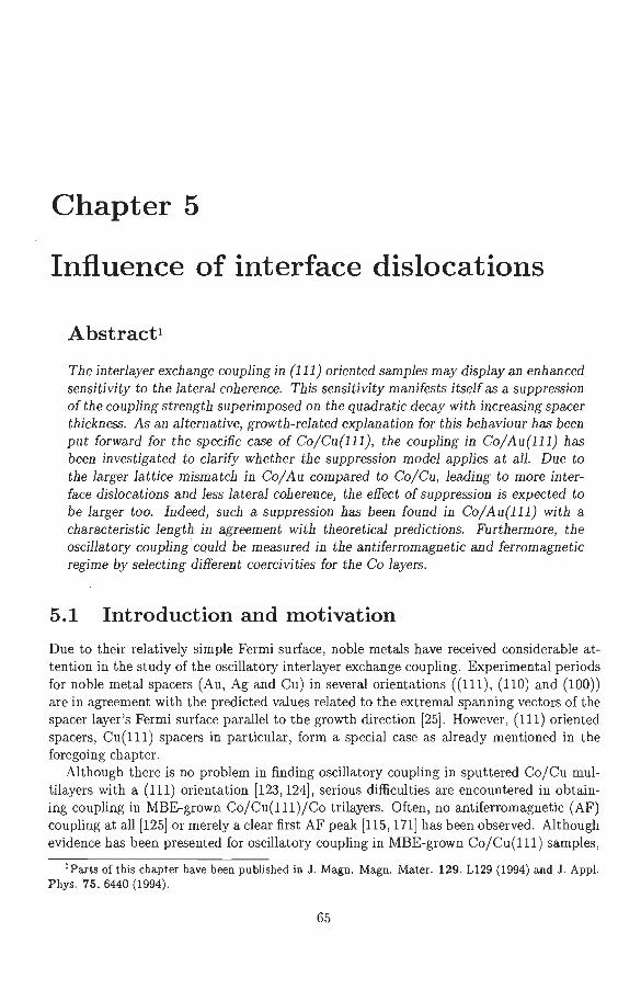
Chapter 5
Influence of interface dislocations
Abstract1
The interlayer exchange coupling in (111) oriented samples may display an enhanced sensitivity to the lateral coherence. This sensitivity manifests itself as a suppression of the coupling strength superimposed on the quadratic decay with increasing spacer thickness. As an alternative, growth-related explanation for this behaviour has been put forward for the specific case of Co/Cu(lll), the coupling in Co/Au(lll) has been investigated to clarify whether the suppression model applies at all. Due to the larger lattice mismatch in Co/Au compared to Co/Cu, leading to more interface dislocations and less lateral coherence, the effect of suppression is expected to be larger too. Indeed, such a suppression has been found in Co/Au(lll) with a characteristic length in agreement with theoretical predictions. Furthermore, the oscillatory coupling could be measured in the antiferromagnetic and ferromagnetic regime by selecting different coercivities for the Co layers.
5.1 Introduction and motivation
Due to their relatively simple Fermi surface, noble metals have received considerable attention in the study of the oscillatory interlayer exchange coupling. Experimental periods for noble metal spacers (Au, Ag and Cu) in several orientations ((111 ), (110) and (100)) are in agreement with the predicted values related to the extremal spanning vectors of the spacer layer's Fermi surface parallel to the growth direction [25]. However, (111) oriented spacers, Cu(lll) spacers in particular, form a special case as already mentioned in the foregoing chapter.
Although there is no problem in finding oscillatory coupling in sputtered Co/Cu multilayers with a (111) orientation [123, 124], serious difficulties are encountered in obtaining coupling in MBE-grown Co/Cu(lll)/Co trilayers. Often, no antiferromagnetic (AF) coupling at all [125] or merely a clear first AF peak [115, 171] has been observed. Although evidence has been presented for oscillatory coupling in MBE-grown Co/Cu(lll) samples,
1Parts of this chapter have been published in J . Magn. Magn . Mater. 129, L129 (1994) and J. Appl. Phys. 75, 6440 (1994).
65
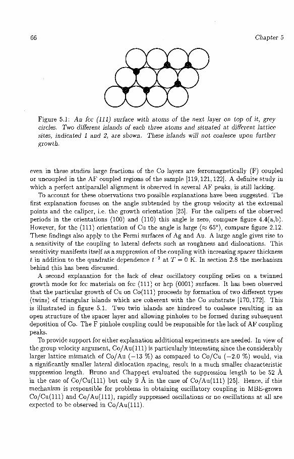
66 Chapter 5
Figure 5.1: An fee (111) surface with atoms of the next layer on top of it, grey circles. Two different islands of each three atoms and situated at different lattice sites, indicated 1 and 2, are shown. These islands will not coalesce upon further growth.
even in these studies large fractions of the Co layers are ferromagnetically (F) coupled or uncoupled in the AF coupled regions of the sample [119, 121, 122]. A definite study in which a perfect antiparallel alignment is observed in several AF peaks, is still lacking.
To account for these observations two possible explanations have been suggested. The first explanation focuses on the angle subtended by the group velocity at the extremal points and the caliper, i.e. the growth orientation [25]. For the calipers of the observed periods in the orientations (100) and (110) this angle is zero, compare figure 4.4(a,b). However, for the (111) orientation of Cu the angle is large (~ 65°), compare figure 2.12. These findings also apply to the Fermi surfaces of Ag and Au. A large angle gives rise to a sensitivity of the coupling to lateral defects such as roughness and dislocations. This sensitivity manifests itself as a suppression of the coupling with increasing spacer thickness t in addition to the quadratic dependence C 2 at T = 0 K. In section 2.8 the mechanism behind this has been discussed.
A second explanation for the lack of clear oscillatory coupling relies on a twinned growth mode for fee materials on fee (111) or hep (0001) surfaces. It has been observed that the particular growth of Cu on Co(lll) proceeds by formation of two different types (twins) of triangular islands which are coherent with the Co substrate [170, 172]. This is illustrated in figure 5.1. Two twin islands are hindered to coalesce resulting in an open structure of the spacer layer and allowing pinholes to be formed during subsequent deposition of Co. The F pinhole coupling could be responsible for the lack of AF coupling peaks.
To provide support for either explanation additional experiments are needed. In view of the group velocity argument, Co/ Au(lll) is particularly interesting since the considerably larger lattice mismatch of Co/ Au (-13 %) as compared to Co/Cu (-2.0 %) would, via a significantly smaller lateral dislocation spacing, result in a much smaller characteristic suppression length. Bruno and Chappert evaluated the suppression length to be 52 A in the case of Co/Cu(lll) but only 9 A in the case of Co/Au(lll) [25]. Hence, if this mechanism is responsible for problems in obtaining oscillatory coupling in MEE-grown Co/Cu(lll) and Co/Au(lll), rapidly suppressed oscillations or no oscillations at all are expected to be observed in Co/Au(lll).
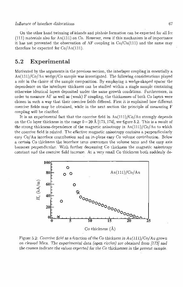
Influence of interface dislocations 67
On the other hand twinning of islands and pinhole formation can be expected for all fee (111) materials also for Au(lll) on Co. However, even if this mechanism is of importance it has not prevented the observation of AF coupling in Co/Cu(lll) and the same may therefore be expected for Co/Au(lll).
5.2 Experimental
Motivated by the arguments in the previous section, the interlayer coupling in essentially a Au(lll)/Co/Au wedge/Co sample was investigated. The following considerations played a role in the choice of the sample composition. By employing a wedge-shaped spacer the dependence on the interlayer thickness can be studied within a single sample containing otherwise identical layers deposited under the same growth conditions. Furthermore, in order to measure AF as well as (weak) F coupling, the thicknesses of both Co layers were chosen in such a way that their coercive fields differed. First it is explained how different coercive fields may be obtained, while in the next section the principle of measuring F coupling will be clarified.
It is an experimental fact that the coercive field in Au(lll)/Co/ Au strongly depends on the Co layer thickness in the range 0- 20 A [173, 174], see figure 5.2. This is a result of the strong thickness-dependence of the magnetic anisotropy in Au(lll)/Co/ Au to which the coercive field is related. The effective magnetic anisotropy contains a perpendicularly easy Co/ Au interface contribution and an in-plane easy Co volume contribution. Below a certain Co thickness the interface term overcomes the volume term and the easy axis becomes perpendicular. With further decreasing Co thickness the magnetic anisotropy constant and the coercive field increase. At a very small Co thickness both suddenly de-
100 0
80 0 0 Au(lll)/Co/ Au
,--. s 60 0 ---..
<r: c <X ~
40 Ooo 0 ooo
20 ooo Ooo Oo
0 •X oooo 0 5 10 15 20 25
Co thickness (A)
Figure 5.2: Coercive field as a function of the Co thickness in Au(ll 1)/Co/ Au grown on cleaved Mica. The experimental data (open circles) are obtained from {173} and the crosses indicate the values expected for the Co thicknesses in the present sample.
68 Chapter 5
Cu(111) +50 A Au +2 A Co
+30 A Au +7 A Co
Figure 5.3: LEED photos of the sample after deposition of additional layers as indicated.
crease again due to the break-up of the continuous Co layer. In this regime the anisotropy is very small as the layered structure disappears. It may lead to a perpendicular easy axis or an in-plane one. Preferably the thinner Co layer should have the lower coercive field as this is the probing layer for the coupling strength. For a thin probing layer even very weak coupling yields reasonably large flip or saturation fields that can be accurately measured, compare equations (2.8) and (2 .10) . This is of particular relevance for Co/ Au(lll) since very weak coupling is expected, based on the expected suppression length of 9 A. The actual thicknesses are indicated in figure 5.2 with a cross.
The exact composition of the MBE-prepared sample is: Cu(111) single crystal/50 A Au/2 A Co/0-40 A Au wedge/7 A Co/20 A Au. The values of the wedge slope obtained from the vibrating quartz crystal and from SAM are 4.1 and 4.0 Ajmm, respectively.
LEED photos were taken in situ after deposition of each layer , see figure 5.3. All LEED photos revealed a sixfold symmetry. The initially sharp, bright spots became increasingly fuzzy with the deposition of subsequent layers. Hence, a fcc (111) structure, or possibly a hcp (0001) structure in the case of Co, and a reduced lateral coherence are concluded . The interspot distance on the LEED photos taken of the Au base and cap layers as well as at various positions on the Au wedge, was 12 ± 1 %smaller than that on the LEED photo of the Cu(111) single crystal. This value agrees with the lattice mismatch between Au and Cu, indicating an approximately complete relaxation of the in-plane lattice spacing of the Au layers and wedge to the bulk value. The interspot distance did not change upon deposition of the 2 A Co layer on the Au base layer. However, to conclude epitaxial coherent growth of this Co layer is too haste as a considerable contribution of the Au base layer to the LEED signal can be present. After deposition of the 7 A Co layer, a
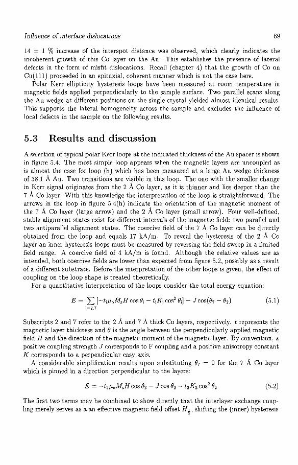
Influence of interface dislocations 69
14 ± 1 % increase of the interspot distance was observed, which clearly indicates the incoherent growth of this Co layer on the Au. This establishes the presence of lateral defects in the form of misfit dislocations. Recall (chapter 4) that the growth of Co on Cu(l 11) proceeded in an epitaxial, coherent manner which is not the case here.
Polar Kerr ellipticity hysteresis loops have been measured at room temperature in magnetic fields applied perpendicularly to the sample surface. Two parallel scans along the Au wedge at different positions on the single crystal yielded almost identical results. This supports the lateral homogeneity across the sample and excludes the influence of local defects in the sample on the following results.
5.3 Results and discussion
A selection of typical polar Kerr loops at the indicated thickness of the Au spacer is shown in figure 5.4. The most simple loop appears when the magnetic layers are uncoupled as is almost the case for loop (h) which has been measured at a large Au wedge thickness of 38.l A Au. Two transitions are visible in this loop. The one with the smaller change in Kerr signal originates from the 2 A Co layer, as it is thinner and lies deeper than the 7 A Co layer. With this knowledge the interpretation of the loop is straightforward. The arrows in the loop in figure 5.4(h) indicate the orientation of the magnetic moment of the 7 A Co layer (large arrow) and the 2 A Co layer (small arrow). Four well-defined, stable alignment states exist for different intervals of the magnetic field: two parallel and two antiparallel alignment states. The coercive field of the 7 A Co layer can be directly obtained from the loop and equals 17 kA/m. To reveal the hysteresis of the 2 A Co layer an inner hysteresis loops must be measured by reversing the field sweep in a limited field range. A coercive field of 4 kA/m is found. Although the relative values are as intended, both coercive fields are lower than expected from figure 5.2, possibly as a result of a different substrate. Before the interpretation of the other loops is given, the effect of coupling on the loop shape is treated theoretically.
For a quantitative interpretation of the loops consider the total energy equation:
E = L [-tiµoMsH cos8i - tiKi cos2 8i] - J cos(81 - 82) (5.1) i=2,7
Subscripts 2 and 7 refer to the 2 A and 7 A thick Co layers, respectively. t represents the magnetic layer thickness and 8 is the angle between the perpendicularly applied magnetic field H and the direction of the magnetic moment of the magnetic layer. By convention, a positive coupling strength J corresponds to F coupling and a positive anisotropy constant K corresponds to a perpendicular easy axis.
A considerable simplification results upon substituting 87 = 0 for the 7 A Co layer which is pinned in a direction perpendicular to the layers:
(5.2)
The first two terms may be combined to show directly that the interlayer exchange coupling merely serves as a an effective magnetic field offset H1 , shifting the (inner) hysteresis
2
70
,......... ~ >, ....,
:g ...., .8' ~ ..... ..... <!)
::::i:::
0.06 (a) 0000000000~>0>0000000:00000
0.00 2.0 A
-0.06 ooocooooooococoocooooocooo
-30 0 . 0.06 (b)
0.00
-0.06
Chapter 5
0.06 (e) 0 .. 0 .o·o -0-0-0-0·00000
o•o .. O""
20.4 A 0.001------~-~---1
o .. o .. o ococo-0-0-0-0·0 o-o-0 ""
-0.06....,,..,,~----±--------= o ~o o ~
0.06 (f) I ,.,,,,,.>O<CCCCC o>o,,,,o,o,_.,~z,c.u-· '
0.00 23.6 A l
0
.,.,.,,,c.cccccocoO _ .. ,11• 1 O<(CCCCCCCC(GC.C.
-0.06 - 00 600 -30 0 30
0.06 (c)
0.00
-0.06
0.06 (g) o-o·O·O··O·O-O•CO:SO~O>
o•o"'
o•O oaoaoao·o-o-o·co o-o-o•
-600 -0.06"-=',.........._~---i,..--------:'
600 -30 0 30
0'06
( d) O·O·O•O•O 0 0 00) 0·0·000•0 COIOI
0.0 I() (h) t ,..,l> t!.>l>ll>l~(((Ol + t t 0)-,))l),~ .. \Clt.: O
0.0 0 38.1 A 18.1 A 0.001---
1~0---+==-"-"---+~
fOlO·O•O•O•O•O·O 0(0 O•O·O 0 0 0 •0•0
-0.06'-=':~-----k-------:::' -0.0
+ ,.l'>ll(.iJll(ClO •+ 6 +··(((((g""'(' .... '"t
-30 0 30 -30 0
field (kA/m)
30
Figure 5.4: Polar Kerr hysteresis loops measured in perpendicularly applied magnetic fields on the 2 A Co/Au(lll) wedge/7 A Co sample. The Au thicknesses corresponding to several positions along the Au wedge are indicted. The solid circles in (f) and (h) indicate where the magnetic field sweep has been reversed to reveal the inner loops. A large and small arrow in (h) indicate the alignment of the moment of the 7 and 2 A Co layers, respectively.
Influence of interface dislocations 71
loop of the 2 A Co layer along the field axis by:
-J H1 =-- (5.3)
2 t2µoMs
The shift will be positive in the case of AF coupling and negative in the case of F coupling. Note that for 07 = w the shifts are in the opposite direction. F coupling can thus be measured by pinning one of the magnetic layers. This may be achieved by a large magnetic anisotropy and a large coercive field, as done here, by indirect coupling to a much thicker third magnetic layer [lll, 132, 138] or direct coupling via exchange biasing. The maximum F coupling that can be measured is determined by the maximum pinning field, which in this case is determined by the coercive field of the 7 A Co layer Hc ,1 :
(5.4)
Sometimes a small correction must be implemented in the above equation. This depends on the precise shape of the (inner) hysteresis loop of the 2 A Co layer , e.g. the coercive field of that layer must be subtracted from Hc,1 for a square hysteresis loop.
From this model, it is clear that the hysteresis loops in figures 5.4(e) and (g) are indicative of F coupling (negative shift) and the loops in (f) and (h) result from AF coupling (positive shift). No inner loops could be measured in loops (e) and (g) because the pinned layer reversed before the anti parallel alignment state was reached. The loops in figures 5.4(a) and ( d) also indicate F coupling. However, in these cases the accompanying negative shift of the inner loop is larger than the pinning field, see equation (5.4), so that the F coupling can not be measured. As a matter of fact , the strength of the F coupling is so large that both layers behave as one magnetic entity with a square hysteresis loop.
At first sight, the loops in figures 5.4(b) and ( c) deviate considerably from the other loops: the transition of the 2 A Co layer is more gradual and extends over a much larger field range (note the larger field scale). This can not be understood within the simplified model given above. Since the coupling at these smaller interlayer thicknesses is expected to be rather strong, the moment of the 7 A Co layer may be forced away from its easy axis when the 2 A Co moment rotates in the applied field, and the assumption 07 = 0 or 7r is no longer valid.
To deal with a varying 07 the total energy equation (5.1) must be considered. Given a set of parameters (J, Ki) the solution (B2 , B1 ) for the minimum energy can be calculated for each field yielding a magnetization loop. From this calculated loop the coupling strength can be determined on the basis of equation (5.3) and compared with the preset value of the coupling strength. By covering a whole range of anisotropy constants and coupling strengths the limitations of equation (5.3) can be investigated.
For the numerical solutions thicknesses t 2 = 0.8 A (60 % reduced magnetic moment, see below) and t7 = 7 A have been used . The magnetic anisotropy K 2 = -0.01 MJ/m3
(in-plane easy axis) has been determined from the measured inner loops. The value of K1 has been varied from approximately 0.05 to 0.5 MJ/m3 (perpendicular easy axis), in accordance with the experimental values of the anisotropy constant of Co/Au(lll) [108, 175, 176] and corresponding to ratios of -K1t1 / K 2t 2 ranging from 50 to 500.
In figure 5.5(a) the coupling strength derived from the simulated loops is plotted against the preset value of the simulation. To determine the coupling strength equation (5.3) has
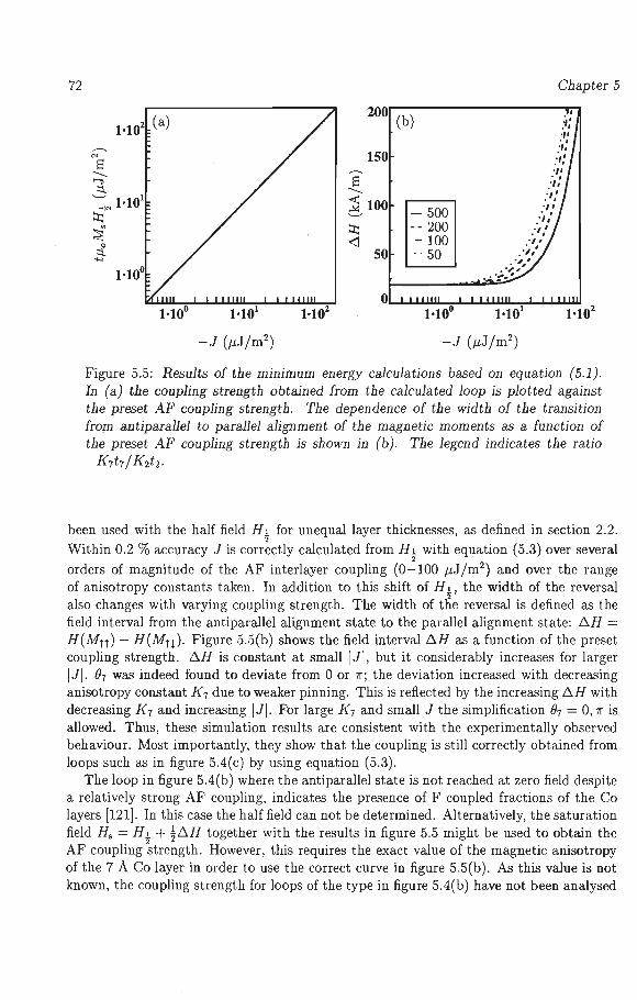
72
-J (µJ/m2)
:.:r:: <I
200 (b)
150
- 500 - - 200 - 100
50 .. 50
Chapter 5
I
:,· .. . , . . . . ,, ... 1,' .,. •I .,,
:, . . . . , . .. . , , :i,' •/I .. ~,' .. ,,, .. ,,
.. "::','
-J (µJjm2)
Figure 5.5: Results of the minimum energy calculations based on equation (5.1). In (a) the coupling strength obtained from the calculated loop is plotted against the preset AF coupling strength . The dependence of the width of the transition from antiparallel to parallel alignment of the magnetic moments as a function of the preset AF coupling strength is shown in (b). The legend indicates the ratio - K1t7f K2t2.
been used with the half field H 1 for unequal layer thicknesses, as defined in section 2.2. 2
Within 0.2 % accuracy J is correctly calculated from H l with equation (5.3) over several 2
orders of magnitude of the AF interlayer coupling (0-100 µJ /m2) and over the range
of anisotropy constants taken. In addition to this shift of H l, the width of the reversal also changes with varying coupling strength. The width of tfi.e reversal is defined as the field interval from the antiparallel alignment state to the parallel alignment state: 6.H = H(Mn) - H(MTl). Figure 5.5(b) shows the field interval 6.H as a function of the preset coupling strength. 6.H is constant at small IJI, but it considerably increases for larger IJI. 87 was indeed found to deviate from 0 or ?r ; the deviation increased with decreasing anisotropy constant K 7 due to weaker pinning. This is reflected by the increasing 6.H with decreasing K 7 and increasing Ill. For large K 7 and small J the simplification 87 = 0, 7r is allowed. Thus, these simulation results are consistent with the experimentally observed behaviour. Most importantly, they show that the coupling is still correctly obtained from loops such as in figure 5.4(c) by using equation (5.3).
The loop in figure 5.4(b) where the antiparallel state is not reached at zero field despite a relatively strong AF coupling, indicates the presence of F coupled fractions of the Co layers [121]. In this case the half field can not be determined. Alternatively, the saturation field H. = H ! + ~6.H together with the results in figure 5.5 might be used to obtain the AF coupling strength. However, this requires the exact value of the magnetic anisotropy of the 7 A Co layer in order to use the correct curve in figure 5.5(b ). As this value is not known, the coupling strength for loops of the type in figure 5.4(b) have not been analysed
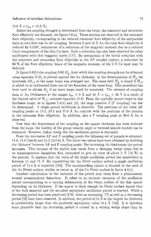
Influence of interface dislocations 73
(9.0 A < tAu < 10.5 A). Before the coupling strength is determined from the loops, the remanent and saturation
Kerr ellipticity are disussed, see figure 5.6(a) . Three minima are observed in the remanent Kerr ellipticity, corresponding to the reduced remanent Kerr ellipticity of the antiparallel state at zero field due to AF coupling. Between 0 and 10 A Au the total Kerr ellipticity is reduced by 0.010°, reminiscent of a reduction of the magnetic moment due to a reduced Cu.rie temperature of the thin Co layer. Such a reduction has also been observed for other multilayers with thin magnetic layers [177]. By comparison of the initial reduction with the remanent and saturation Kerr ellipticity in the AF coupled regions, a reduction by 60 % of the Kerr ellipticity, hence of the magnetic moment , of the 2 A Co layer may be deduced.
In figure 5.6(b) the coupling field H1, from which the coupling strength can be obtained 2
using equation (5.3), is plotted against the Au thickness. In the determination of H1 the hysteresis 2Hc,2 of the inner loops was averaged out. The same field H! is found if Hc,2
2 is added to or subtracted from one of the branches of the inner loop. Tliis procedure has been used to obtain H 1 if no inner loops could be measured. The absence of coupling
2
data at Au thicknesses in the ranges tAu < 9 A and 15 A < tAu < 20 A is a result of the limited value of Hc,7 , compare equation (5.4). From the typically square loops in this thickness range, as in figures 5.4(a) and (d), the large positive J (F coupling) can not be determined. A single period oscillation is observed. The positions of the three AF coupling peaks at 12.2, 23.2 and 37.6 A Au coincide with the positions of the minima in the remanent Kerr ellipticity. In addition, also a F coupling peak at 30.0 A Au is observed.
Now that the dependence of the coupling on the spacer thickness has been deduced from the loops, the validity of the group velocity angle or twinned islands models can be evaluated. However, before doing this the oscillation period is discussed .
From the successive AF and F coupling peaks the following set of periods is obtained: 11.0, 13.6 (2x6.8) and 15.2 (2x7.6) A. The latter two values have been obtained by doubling the 'distance' between AF and F coupling peaks. For increasing Au thicknesses the period increases. This increase of the period may result from a changing wedge slope due to an inhomogeneous deposition flux, estimated to give an error of about 2 A (15 %) in the periods. It appears that the value of the single oscillation period lies somewhere in between 11 and 15 A. By considering the Au Fermi surface indeed a single oscillation period of 11.4 A is expected [163]. The corresponding caliper is situated at the neck of the Au Fermi surface, similar to vector q 1 of the Cu Fermi surface in figure 4.4( c).
Another contribution to the variation of the period may come from a phenomenon termed preasymptotic behaviour. It refers to an intrinsic variation of the oscillation period corresponding to a varying deformation of the Fermi surface of the thin spacer depending on its thickness. If the spacer is thick enough its Fermi surface equals that of the bulk material and the so-called asymptotic oscillation period is reached. While a decreasing period has been predicted [178], both an increasing [77] as well as a decreasing period [78] have been observed . In addition, the period of 15 A at the largest Au thickness is considerably larger than the predicted asymptotic value 11.4 A [163]. It is therefore more plausible that the increasing period is caused by a varying wedge slope than by
74
0.06
0·28
10 s ---.:x:: ..:.:: 0 ...._,
_,"' ::i:: I
-10
-~8
10 ,-., ~ 0
..... "" I
-10 0 .......
" -20 N<( -'""':>
-30
-40
F
0
0
AF Oo
10
o x O.l
0 0
, O'
O"
, ,
0
, ,
0
' ...
, ,
20
Au thickness (A)
(a)
~ ~
(b)
(c)
30 40
Chapter 5
Figure 5.6: (a) Remanent (solid circles) and saturation Kerr ellipticity (open circles) as a function of the Au wedge thickness. (b) Half field versus the Au wedge thickness. (c) Coupling strength multiplied by the Au wedge thickness squared versus the Au wedge thickness. The dashed envelope is a guide to the eye.
Influence of interface dislocations 75
preasymptotic behaviour. A maximum AF coupling strength of J = -0.026 mJ/m2 is found at 12.2 A Au. In
this evaluation of the maximum AF coupling strength the reduced moment has been accounted for. This value is of the same order as reported values for Ni0.8Fe0.2/Au(lll) with -0.020 mJ/m2 and Co/Au(lll) with -0.055 mJ/m2 [107,179] . Comparison with the latter Co/Au(lll) result suggests that the sample investigated here contains more defects which reduce the coupling strength .
The observation of coupling itself does not discriminate between the two cases of Co/Cu(lll) and Co/Au(lll). It is the observation of several coupling peaks in the case of Co/Au(lll) that contrasts with the absence of higher order peaks for Co/Cu(lll). From this one would conclude that the suppression length in Co/Cu(lll) is shorter than in Co/ Au(lll), opposite to the predicted situation. Therefore, the suppression of the coupling due to lateral misfit dislocations in relation with a large angle between the group velocity and the caliper, is not expected to be responsible for the absence of higher order AF peaks in Co/Cu(lll). Nevertheless, a suppression length can be estimated from the measured peaks in Co/ Au(lll). ·
To observe an additional suppression of the coupling strength as a function of the spacer thickness tAu on top of the expected quadratic decay (:\~, it is useful to plot Jt'iu against tAu· The result is given in figure 5.6(c). Although beyond the first maximum (tAu > 17 A) the data are consistent with a (:\~-dependence, it is clear that the coupling strength initially decreases more rapidly with Au interlayer thickness than (:\~·
It is unlikely that an error in the start of the wedge is responsible for this behaviour (compare section 4.3), as an offset of 2.5 mm or 10 A Au would be required to compensate the initial rapid decrease. Furthermore, the effect on the thickness-dependence of the finite temperature - the measurements were carried out at room temperature - is also by far not able to account for the decrease of the coupling strength in addition to the quadratic decay. With the help of figure 2.15 the values for Au(lll) can be obtained by implementing an extra factor of 2 in the horizontal scale [163]. The effect of the temperature estimated in section 2.11 for Cu(lOO) (not more than 10 % reduction at room temperature) is still representative for the effect in the case of Au(lll). Therefore, the initial rapid decrease with a characteristic length of typically 10 A Au, supports the model of Bruno and Chappert , who calculated a suppression (cut-off) length of 9 A [25] . The agreement may be fortunate, however , as other defects than misfit dislocations can also play a role, see below.
Other investigations of the coupling across (111) spacers support this conclusion. For example, in Fe(llO)/Ag(lll) also an oscillatory exchange coupling has been observed with 4 AF peaks [76]. Along the Ag[TlO] axis the lattice mismatch is small (-0.9%), but it is 19.l % in the direction of the Ag[112] axis. On the basis of the latter value, the group velocity angle argument would lead to a rapid suppression of the coupling. Nevertheless, several oscillation peaks have been measured. For Au(lll) a similar investigation has been carried out by Grolier et al. whiCh corroborated these results [107].
It appears that a suppression mechanism exists, however , its origin in misfit dislocations cannot explain the absence of AF peaks in Co/Cu(lll) in the light of the new results. Other origins of this suppression mechanism such as roughness or steps at the interfaces
76 Chapter 5
may play a role. Furthermore, also defects within the spacer volume will lead to stronger suppression of the coupling when the group velocity subtends a larger angle with the caliper. This has been discussed in section 2.8 . One of these volume defects is formed by the twinned island structure, which will also lead to a suppression of the coupling.
Regarding the explanation of the absence of coupling based on the twinned island growth and pinhole formation, the following remark is made. It is plausible that for thicker spacer layers it becomes increasingly unlikely that that pinholes can form a ferromagnetic bridge across the spacer. For this reason pinholes are expected to obscure the AF coupling mainly at small spacer thickness but not at large thickness, as observed. However, if one considers a competition between direct F coupling through pinholes and indirect AF coupling through the spacer, it is clear that for higher order and weaker AF peaks pinhole coupling will more easily dominate. Such a model has been developed and can qualitatively explain why higher order AF peaks tend to be absent [180]. However, for a quantitative explanation a careful study of growth defects, e.g. with NMR [181, 182], in Co/Au(lll) and Co/Cu(lll) is required.
5 .4 Conclusions
In agreement with theory, a single long oscillation period has been found for a MBEgrown Co/Au(lll)/Co sandwich. By using Co layers with different coercive fields both AF and F coupling could be measured . The experimental period ranges from 11 to 15 A which interval includes the theoretical period of 11.4 A. Furthermore, the existence of a significant suppression of the coupling strength as a function of the spacer thickness in addition to the quadratic decay, has been established. The characteristic length of suppression, approximately 10 A, also agreed with the theoretical value of 9 A, predicted from a model that considers the effect of misfit dislocations. Finally, these results indicate that the lattice mismatch in combination with a suppression mechanism based on the non-zero angle between the goup velocity at the extremal points and the caliper, can not explain the failure to observe clear oscillations of the coupling in Co/Cu(lll) MBE-grown samples.
Chapter 6
Magnetic layer thickness-dependence
Abstract 1
The dependence of the interlayer exchange coupling on the thickness of the magnetic layers in essentially a Co/Cu/Co sample has been investigated. Similar to the dependence on the spacer thickness an oscillatory behaviour is obtained but with a smaller amplitude. This observation substantiates claims that the interlayer exchange coupling is related to multiple reflections of electron waves in the whole multilayer stack. The predicted period of the oscillation stems from a caliper of the Co Fermi surface and agrees with the observed period.
6.1 Introduction and motivation
Although the multiplicity and the values of the periods are fairly well understood for the monovalent noble metal interlayers and, be it somewhat less, for the 4d and 5d element spacers, the role of the magnetic layer in determining the interlayer exchange coupling has not been clarified so far. In a first experiment Qui et al. have studied the coupling behaviour in three separate (001) Co/Cu/Co sandwiches with different Co layer thicknesses, and concluded that the coupling was a pure interface effect, i.e. independent of the Co layer thickness [112]. However, theoretical predictions by Bruno [48] and Barna.S [50, 51] have shown that the magnetic coupling may oscillate with the ferromagnetic layer thickness, as discussed in section 2.9. To observe such an oscillation wedge-shaped ferromagnetic layers have been used, covering a whole range of thicknesses. In this way an unfortunate choice of a few separate constant thicknesses, appearing to support an independent behaviour, can be avoided.
6.2 Experimental
The availability of high quality, single crystalline Cu substrates, the growth experience and the success in obtaining oscillatory coupling as a function of the interlayer thickness,
1Parts of this chapter have been published in Phys. Rev. Lett. 72, 764 (1994)
77
78 Chapter 6
motivated the choice to study the effect of the magnetic layer in a fee (001) Co/Cu/Co sandwich grown by MBE on a single crystal Cu(OOl) substrate . A dedicated, multiple wedge sample has been employed to allow for independent investigation of the Cu and Co thickness-dependence of the coupling across Cu(OOl) in a single sample. In this study of the dependence on the magnetic layer thickness it is of course necessary to have a Co wedge. To maintain a symmetric sandwich as much as possible two almost identical Co wedges have been used. In addition, a Cu wedge has been grown as the interlayer exchange coupling strongly depends on the Cu spacer thickness. This allows a preceding verification of the coupling behaviour as a function of the Cu thickness and the tuning of the Cu thickness to maximum antiferromagnetic (AF) coupling when investigating the Co thickness-dependence. For independent variation the Co and Cu wedges are oriented perpendicularly with respect to each other. Two samples have been prepared (shown schematically in figure 6.1), with the following compositions:
I: Cu(l00)/50 Co+l5 Ni+0-20 Co (2.3)/0-40 Cu (5.0)/ 0-20 Co (2.3)+15 Ni+50 Co/7 Cu+20 Au,
II: Cu(l00)/30 Co+l5 Ni+O - 20 Co (2.3) 0 - 25 Cu (3.1)/ 0 - 20 Co (2.3)+15 Ni+30 Co/7 Cu+20 Au.
All thicknesses are in A and the wedge slopes in parentheses are in A/mm. The reason for the additional uniform Co and Ni layers which seem, at first sight, unnecessary for the experiment, will be discussed later on.
The structure of the layers has been investigated with LEED and yielded results consistent with earlier observations, see section 4.2 [90, 113] . In summary, the Cu wedge displays an identical lattice constant to that of the Cu substrate and maintains an fee structure. LEED investigations directly after the growth of the second Co wedge revealed that the Co displays an identical surface lattice to the Cu, i.e. the Co grows in-plane expanded, and grows with a face centered tetragonal structure. As a result of the inplane expansion, the perpendicular Co-Co lattice constant (1.70 ± 0.02 A) appeared to be reduced by around 4 % with respect to the bulk value (1.78 A). However, it is important to note that this situation is not expected to be maintained until after the samples are completed, i.e. after the growth of the additional Ni and Co layers on top of the Co wedge. Instead a relaxation of the strain is to be expected to occur above a certain critical thickness. This was confirmed by our LEED observations which showed that the top uniform Co layer was almost completely relaxed to its bulk lattice spacing. Since this relaxation is commonly assumed to be uniform throughout the layer the structure of the Co wedge is also expected to be close to the bulk fee phase.
The AF coupling behaviour has been investigated at room temperature by measuring magnetic hysteresis loops at various positions on the sample via the longitudinal MOKE. The additional Co and Ni layers have been employed to enable such measurements at the very low Co wedge thicknesses, i.e. to enhance the MOKE signals that otherwise would have been too small because of the combined effect of their scaling with magnetic layer thickness and the additional reduction in signal associated with a lowering of the Curie temperature with decreasing Co thickness [113]. In addition, thin ferromagnetic layers may lead to flip fields larger than the available magnetic field, compare equation (2.10), and prevent determination of the coupling strength. A uniform Ni layer has been

Magnetic layer thickness-dependence
Co Ni
Co wedge
Cu wedge
Co wedge , Ni
Co
Cu(lOO)
Figure 6.1: Stacking sequence and relative wedge orientations for the samples. Mutually perpendicular Co and Cu wedges have been used to allow for independent investigation of the Cu and Co layer thickness-dependence of the interlayer exchange coupling in a single sample. The uniform Ni (15 A) and Co layers (50 A for sample I and 30 A for sample II) have been employed to eliminate problems related to small MOKE signals and high flip fields at low Co wedge thicknesses. For clarity the cap layers have been omitted. In practice the thickness of the wedges does not vary continuously, as drawn , but more step-like and with islands. Furthermore the actual sample is disk-shaped and not square.
79
added adjacent to each Co wedge and not a uniform Co layer because the latter would yield an offset in the Co thickness. This is unwanted since the largest Co thicknessdependent effects are to be expected at low Co thicknesses, equation (2.49) [48, 50, 51] . Of course the Ni layers may affect the coupling but, as will be explained below, this concerns only the amplitude and the phase but not the period of an oscillation with varying Co thickness. Finally, the uniform Co layers that have been added at the outer part of the sandwich merely serve to maintain an optimal accuracy in the determination of the coupling strength: Co(OOl) layers exhibit a relatively large cubic in-plane anisotropy, leading to an abrupt well-defined transition from the antiparallel state to the saturated parallel state, cf. the loop in figure 2.3(c) [18]. The rather low cubic in-plane anisotropy of Ni(OOl), on the other hand, would have led to a gradually increasing magnetization, as in the loop in figure 2.3(a), from which it would have been considerably. more difficult to accurately determine the coupling strength. Although the samples may seem complicated because of these additional layers it is clear that to enable accurate room temperature MOKE experiments at very small Co wedge thicknesses, these layers are crucial.
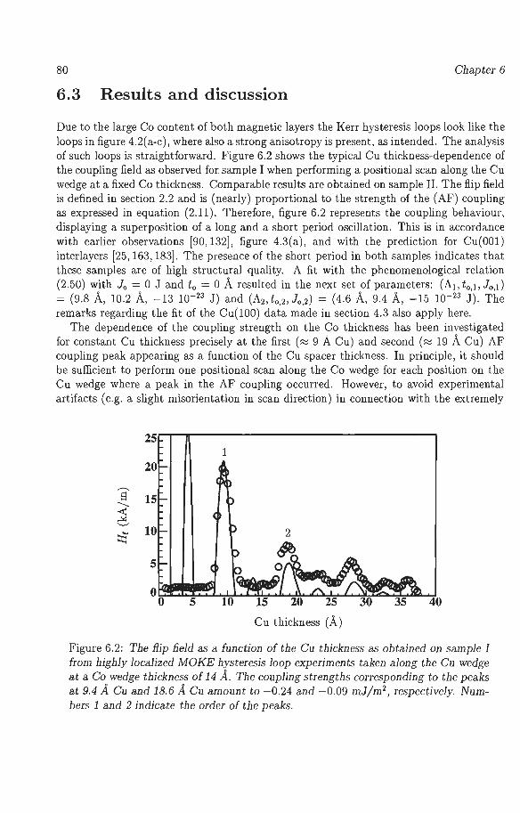
80 Chapter 6
6.3 Results and discussion
Due to the large Co content of both magnetic layers the Kerr hysteresis loops look like the loops in figure 4.2(a-c), where also a strong anisotropy is present, as intended. The analysis of such loops is straightforward. Figure 6.2 shows the typical Cu thickness-dependence of the coupling field as observed for sample I when performing a positional scan along the Cu wedge at a fixed Co thickness. Comparable results are obtained on sample II . The flip field is defined in section 2.2 and is (nearly) proportional to the strength of the (AF) coupling as expressed in equation (2.11) . Therefore, figure 6.2 represents the coupling behaviour, displaying a superposition of a long and a short period oscillation. This is in accordance with earlier observations [90, 132], figure 4.3(a), and with the prediction for Cu(OOl) interlayers [25, 163, 183]. The presence of the short period in both samples indicates that these samples are of high structural quality. A fit with the phenomenological relation (2.50) with J0 = 0 J and t0 = 0 A resulted in the next set of parameters: (A1 , t0 ,1, J0 , 1 )
= (9.8 A, 10.2 A, -13 10- 23 J) and (A2, to,21 lo,2) = (4.6 A, 9.4 A, -15 10-23 J). The remarks regarding the fit of the Cu(lOO) data made in section 4.3 also apply here.
The dependence of the coupling strength on the Co thickness has been investigated for constant Cu thickness precisely at the first (:::::: 9 A Cu) and second (:::::: 19 A Cu) AF coupling peak appearing as a function of the Cu spacer thickness. In principle, it should be sufficient to perform one positional scan along the Co wedge for each position on the Cu wedge where a peak in the AF coupling occurred. However, to avoid experimental artifacts (e.g. a slight misorientation in scan direction) in connection with the extremely
25 1
20
,--._
El 15 -......... ~ ~ .__,
~ 10
5
0 0 5
Cu thickness (A)
Figure 6.2: The flip field as a function of the Cu thickness as obtained on sample I from highly localized MOKE hysteresis loop experiments taken along the Cu wedge at a Co wedge thickness of 14 A. The coupling strengths corresponding to the peaks at 9.4 A Cu and 18.6 A Cu amount to -0.24 and - 0.09 mJ/m2
, respectively. Numbers 1 and 2 indicate the order of the peaks.
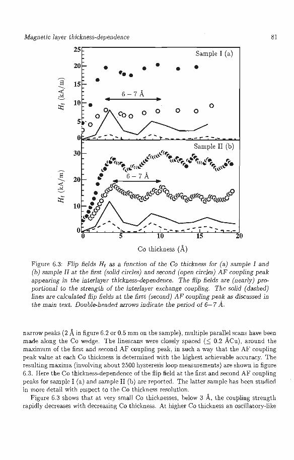
Magnetic layer thickness-dependence
25 Sample I (a)
20 • • • • • •• • ,..-... • s 15 .....__ <C 6-7A ~ ...__,
~ 10 • 0
0 0 0 0
---..........
10 15 20
Co thickness (A)
Figure 6.3: Flip fields Hr as a function of the Co thickness for (a) sample I and (b) sample II at the first (solid circles) and second (open circles) AF coupling peak appearing in the interlayer thickness-dependence. The flip fields are (nearly) proportional to the strength of the interlayer exchange coupling. The solid (dashed) lines are calculated flip fields at the first (second) AF coupling peak as discussed in the main text. Double-headed arrows indicate the period of 6- 7 A.
81
narrow peaks (2 A in figure 6.2 or 0.5 mm on the sample), multiple parallel scans have been made along the Co wedge. The linescans were closely spaced (~ 0.2 ACu), around the maximum of the first and second AF coupling peak, in such a way that the AF coupling peak value at each Co thickness is determined with the highest achievable accuracy. The resulting maxima (involving about 2500 hysteresis loop measurements) are shown in figure 6.3. Here the Co thickness-dependence of the flip field at the first and second AF coupling peaks for sample I (a) and sample II (b) are reported. The latter sample has been studied in more detail with respect to the Co thickness resolution.
Figure 6.3 shows that at very small Co thicknesses, below 3 A, the coupling strength rapidly decreases with decreasing Co thickness. At higher Co thickness an oscillatory-like
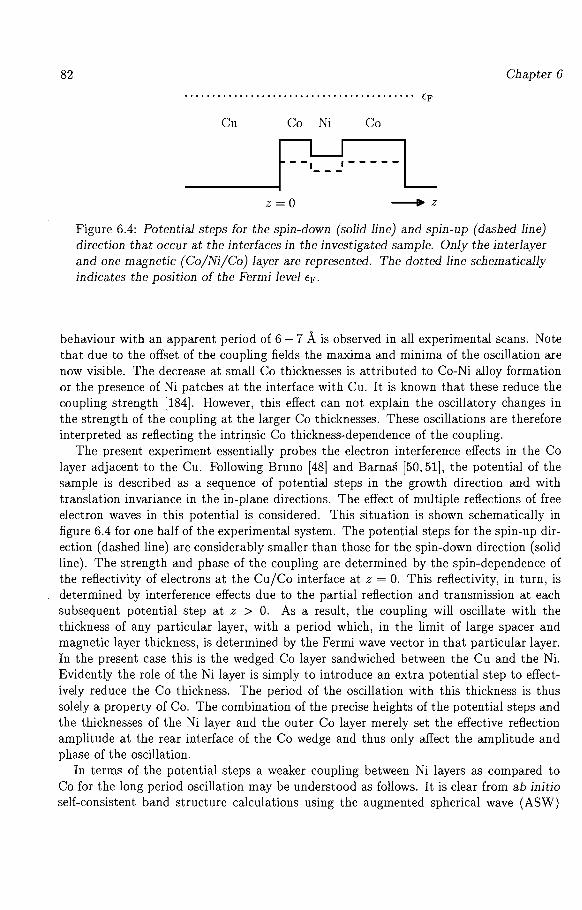
82 Chapter 6
•••••••••••••••••••••••••••••••••••••••••• EF
Cu Co Ni Co
·- - _. - - - - -
z=O --+ z
Figure 6.4: Potential steps for the spin-down (solid line) and spin-up (dashed line) direction that occur at the interfaces in the investigated sample. Only the interlayer and one magnetic (Co/Ni/Co) layer are represented. The dotted line schematically indicates the position of the Fermi level EF.
behaviour with an apparent period of 6 - 7 A is observed in all experimental scans. Note that due to the offset of the coupling fields the maxima and minima of the oscillation are now visible. The decrease at small Co thicknesses is attributed to Co-Ni alloy formation or the presence of Ni patches at the interface with Cu. It is known that these reduce the coupling strength [184]. However, this effect can not explain the oscillatory changes in the strength of the coupling at the larger Co thicknesses. These oscillations are therefore interpreted as reflecting the intrinsic Co thickness-dependence of the coupling.
The present experiment essentially probes the electron interference effects in the Co layer adjacent to the Cu. Following Bruno [48] and Barn&§ [50, 51], the potential of the sample is described as a sequence of potential steps in the growth direction and with translation invariance in the in-plane directions. The effect of multiple reflections of free electron waves in this potential is considered. This situation is shown schematically in figure 6.4 for one half of the experimental system. The potential steps for the spin-up direction (dashed line) are considerably smaller than those for the spin-down direction (solid line). The strength and phase of the coupling are determined by the spin-dependence of the reflectivity of electrons at the Cu/Co interface at z = 0. This reflectivity, in turn, is determined by interference effects due to the partial reflection and transmission at each subsequent potential step at z > 0. As a result, the coupling will oscillate with the thickness of any particular layer, with a period which, in the limit of large spacer and magnetic layer thickness, is determined by the Fermi wave vector in that particular layer. In the present case this is the wedged Co layer sandwiched between the Cu and the Ni. Evidently the role of the Ni layer is simply to introduce an extra potential step to effectively reduce the Co thickness. The period of the oscillation with this thickness is thus solely a property of Co. The combination of the precise heights of the potential steps and the thicknesses of the Ni layer and the outer Co layer merely set the effective reflection amplitude at the rear interface of the Co wedge and thus only affect the amplitude and phase of the oscillation.
In terms of the potential steps a weaker coupling between Ni layers as compared to Co for the long period oscillation may be understood as follows. It is clear from ab initio self-consistent band structure calculations using the augmented spherical wave (ASW)
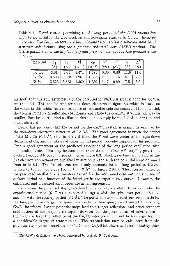
Magnetic layer thickness-dependence
Table 6.1: Fermi vectors pertaining to the long period of the (100) orientation and the potential in the free electron approximation relative to Cu for the given materials. The Fermi vectors have been obtained from ab initio self-consistent band structure calculations using the augmented spherical wave (ASW) method. The lattice parameters of the in-plane (a11) and perpendicular (a.i) lattice parameter are indicated.
material au a.i kl e vi vr Al AT F F
(A) (A) (A-1) (A-1) (eV) (eV) (A) (A) Cu fee 3.61 3.61 1.471 1.471 0.00 0.00 11.6 11.6 Co fee 3.538 3.538 1.261 1.363 2.18 1.16 6.1 7.6 Ni fee 3.523 3.523 1.362 1.389 1.17 0.89 7.5 8.0
83
method 1 that the spin asymmetry of the potential for Ni/ Cu is smaller than for Co/Cu, see table 6.1. This can be seen for spin-down electrons in figure 6.4 which is based on the values in this table. As a consequence of the smaller spin asymmetry of the potential, the spin asymmetry of reflection coefficients and hence the coupling strength will also be smaller. For the short period oscillation this can not simply be concluded, but this period is not observed.
Bruno has proposed that the period for the Co/Cu system is mainly determined by the spin-down electronic structure of Co [48] . The good agreement between the period of 3.5 ML Co (6.2 A), that he derived from the Fermi wave vector of the spin-down electrons of Co, and our observed experimental period, provides support for his proposal. Even a good agreement of the predicted amplitude of the long period oscillation with our results exists. This may be concluded from the solid (first AF coupling peak) and dashed (second AF coupling peak) lines in figure 6.3, which have been calculated in the free electron approximation explained in section 2.6 and with the potential steps obtained from table 6.1. The free electron result only accounts for the long period oscillation related to the caliper along rx at k11 = 0 A- 1 in figure 2.9(b). The incorrect offset of the predicted oscillations is therefore caused by the additional constant contribution of a short period as a function of the interlayer in the experimental curves. However, the calculated and measured amplitudes are in fair agreement.
Once more the potential steps, tabulated in table 6.1 , are useful to explain why the experimental period (6-7 A) is expected to agree with the spin-down period (6.1 A) and not with the spin-up period (7.6 A). The potential steps for electrons responsible for the long period are larger for spin-down electrons than spin-up electrons at Cu/Co and Co/Ni interfaces. Larger potential steps lead to stronger reflections and hence stronger modulations of the coupling strength. However, for the present case of interference in the magnetic layer the reflection at the Cu/Co interface should not be too large, leaving a considerable degree of transmission. The transmission may be calculated from the potential steps to be around 0.9 for Cu/ Co and Co/Ni interfaces and semi-infinitely thick
1The ASW calculations have been performed by prof. dr. R. Coehoorn.
84 Chapter 6
layers. Therefore, judging from the stronger reflection of the spin-down electrons these spin-down electrons will dominate the oscillatory behaviour.
A reason for keeping some reserve with respect to the good agreement is that for the low Co thicknesses here, the asymptotic thickness limit, where the Fermi wave vector determines the period, might not have been approached sufficiently close. The fact that no clear third peak is observed can be related to unequal wedge slopes and starts. It has been pointed out that this leads to interference of the oscillation as a function of the thickness of one Co wedge with that of the other [147].
6.4 Conclusions
In conclusion, a clear dependence has been demonstrated of the strength of the coupling across Cu(OOl) on the Co thickness suggesting an oscillatory behaviour with a period of 6 - 7 A Co. This period is in good agreement with the predicted period by Bruno [48] on the basis of the extremal wave vector spanning the ellipsoidal hole pocket centered at the X-point of the spin-down Fermi surface of fee Co. These results provide strong evidence for the quantum interference models for interlayer exchange coupling. Application of these models shows that the present type of exchange coupling experiments yield spin selective information on the Fermi surfaces of ferromagnetic materials.
Chapter 7
Cap layer thickness-dependence
Abstract 1
In support of the prediction that the interlayer exchange coupling oscillates with the thickness of any layer, the experiments in this chapter show an oscillation of the coupling strength as a function of the non-magnetic cap layer in a Co/Cu spacer/Co/Cu cap sample. The relative phase and amplitude of the oscillation at various thicknesses of the spacer agree with an analytical approximate expression derived from the Bruno model.
7 .1 Introduction and motivation
The Bruno model describes the coupling between magnetic (multi)layers across a nonmagnetic spacer layer in terms of spin-dependent effective reflection of electron waves at the interfaces of the spacer [48, 52]. These effective reflection coefficients, in turn, depend on multiple reflections within the constituent layers of the magnetic multilayers and other back layers. The model implies that each layer in an entire multilayer stack is relevant to the coupling. Predictions of an oscillatory dependence of the coupling strength on the magnetic layer thickness have been corroborated by experiments on Co/Cu(lOO), see also chapter 6, Fe/Cr(lOO) and Fe/ Au(lOO) sandwiches [114, 148, 149]. The effect of base, seed or cap layer thicknesses on the coupling strength has not been investigated yet.
An indication for the existence of such an effect follows from experiments on Au(lOO) base/Fel/ Au spacer/Fe2/ Au cap by Okuno and Inomata [149]. Their results are schematically presented in figure 7.1. Essentially, the dependence of the coupling on the magnetic layer thickness has been studied using two stepped wedges with 1 ML steps. In some cases the upper and lower wedges did not coincide but were relatively shifted half a terrace length in the direction of the thickness gradient and in the opposite direction (situations 1 and 2 in figure 7.1). If one compares the observed oscillation of these two situations, it appears that they are phase-shifted by 1r. The experiment may be viewed upon as if one situation follows from the other by interchanging the two Fe layers. Ideally, this is
1 Parts of this chapter have been published in Phys. Rev. Lett . 75, 4306 (1995)
85
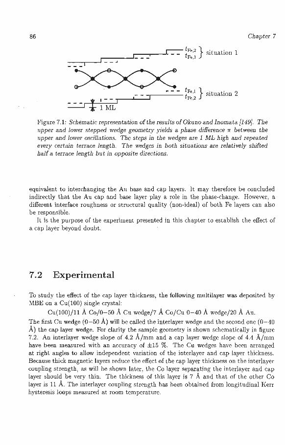
86
r:-:- tFe,2 } situation 1 --......--_,ir-_-_-,,---'i,...._-_-_...--.... tFe,J
.. - - tFe,I } situation 2 tFe,2
Chapter 7
Figure 7.1: Schematic representation of the results of Okuno and Inomata {149} . The upper and lower stepped wedge geometry yields a phase difference 7f between the upper and lower oscillations. The steps in the wedges are 1 ML high and repeated every certain terrace length. The wedges in both situations are relatively shifted half a terrace length but in opposite directions.
equivalent to interchanging the Au base and cap layers. It may therefore be concluded indirectly that the Au cap and base. layer play a role in the phase-change. However, a different interface roughness or structural quality (non-ideal) of both Fe layers can also be responsible.
It is the purpose of the experiment presented in this chapter to establish the effect of a cap layer beyond doubt.
7.2 Experimental
To study the effect of the cap layer thickness, the following multilayer was deposited by MBE on a Cu(lOO) single crystal:
Cu(l00)/11 A Co/0-50 A Cu wedge/7 A Co/Cu 0-40 A wedge/20 A Au.
The first Cu wedge (0-50 A) will be called the interlayer wedge and the second one (0-40 A) the cap layer wedge. For clarity the sample geometry is shown schematically in figure 7.2. An interlayer wedge slope of 4.2 A/mm and a cap layer wedge slope of 4.4 A/mm have been measured with an accuracy of ±15 %. The Cu wedges have been arranged at right angles to allow independent variation of the interlayer and cap layer thickness. Because thick magnetic layers reduce the effect of the cap layer thickness on the interlayer coupling strength, as will be shown later, the Co layer separating the interlayer and cap layer should be very thin. The thickness of this layer is 7 A and that of the other Co layer is 11 A. The interlayer coupling strength has been obtained from longitudinal Kerr hysteresis loops measured at room temperature.
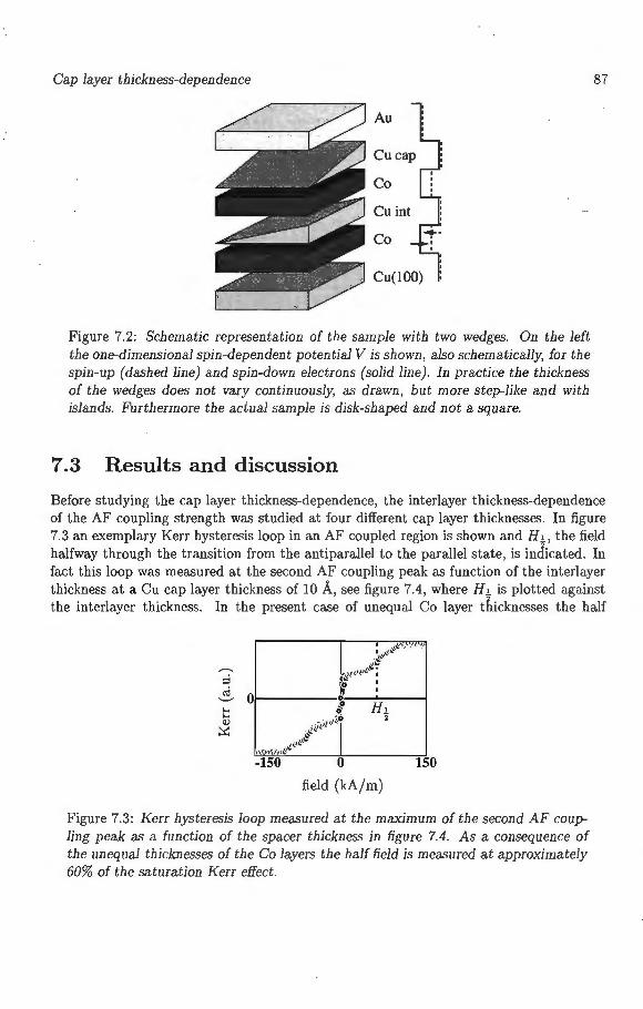
Cap layer thickness-dependence
Co
Cu int
Co
Cu(lOO)
Figure 7.2: Schematic representation of the sample with two wedges. On the left the one-dimensional spin-dependent potential V is shown, also schematically, for the spin-up (dashed line) and spin-down electrons (solid line). In practice the thickness of the wedges does not vary continuously, as drawn, but more step-like and with islands. Furthermore the actual sample is disk-shaped and not a square.
7 .3 Results and discussion
87
Before studying the cap layer thickness-dependence, the interlayer thickness-dependence of the AF coupling strength was studied at four different cap layer thicknesses . In figure 7.3 an exemplary Kerr hysteresis loop in an AF coupled region is shown and Hi, the field halfway through the transition from the antiparallel to the parallel state, is indicated. In fact this loop was measured at the second AF coupling peak as function of the interlayer thickness at a Cu cap layer thickness of 10 A, see figure 7.4, where H1 is plotted against the interlayer thickness. In the present case of unequal Co layer thicknesses the half
-150 0 150
field (kA/m)
Figure 7.3: Kerr hysteresis loop measured at the maximum of the second AF coupling peak as a function of the spacer thickness in figure 7.4. As a consequence of the unequal thicknesses of the Co layers the half field is measured at approximately 60% of the saturation Kerr effect.
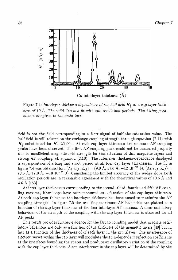
88 Chapter 7
70
60
50 ,--.
s 40 .....__ <t:: c 30 ~'"'
::x:: 20
10
Cu interlayer thickness (A)
Figure 7.4: Interlayer thickness-dependence of the half field H 1 at a cap layer thick-2
ness of 10 A. The solid line is a fit with two oscillation periods. The fitting para-meters are given in the main text.
field is not the field corresponding to a Kerr signal of half the saturation value. The half field is still related to the exchange coupling strength through equation (2.11) with H 1 substituted for Hr [20, 90]. At each cap layer thickness five or more AF coupling pe~ks have been observed. The first AF coupling peak could not be measured properly due to insufficient magnetic field strength for this situation of thin magnetic layers and strong AF coupling, cf. equation (2.10). The interlayer thickness-dependence displayed a superposition of a long and short period at all four cap layer thicknesses. The fit in figure 7.4 was obtained for: (A1, t0 ,i, J0 ,1) = (9.0 A, 17.0 A, -12 10-23 J), (A2, t0 ,2, 10 ,2) = (3.6 A, 17.0 A, -10 10-23 J). Considering the limited accuracy of the wedge slope both oscillation periods are in reasonable agreement with the theoretical values of 10.6 A and 4.6 A [163].
At interlayer thicknesses corresponding to the second, third, fourth and fifth AF coupling maxima, Kerr loops have been measured as a function of the cap layer thickness. At each cap layer thickness the interlayer thickness has been tuned to maximize the AF coupling strength. In figure 7.5 the resulting maximum AF half fields are plotted as a function of the cap layer thickness at the four interlayer AF maxima. A clear oscillatory behaviour of the strength of the coupling with the cap layer thickness is observed for all AF peaks.
This result provides further evidence for the Bruno coupling model that predicts oscillatory behaviour not only as a function of the thickness of the magnetic layers [48] but in fact as a function of the thickness of of each layer in the multilayer. The interference of electron waves within the cap layer will modulate the spin-dependent reflection coefficients at the interfaces bounding the spacer and produce an oscillatory variation of the coupling with the cap layer thickness. Since interference in the cap layer will be determined by the
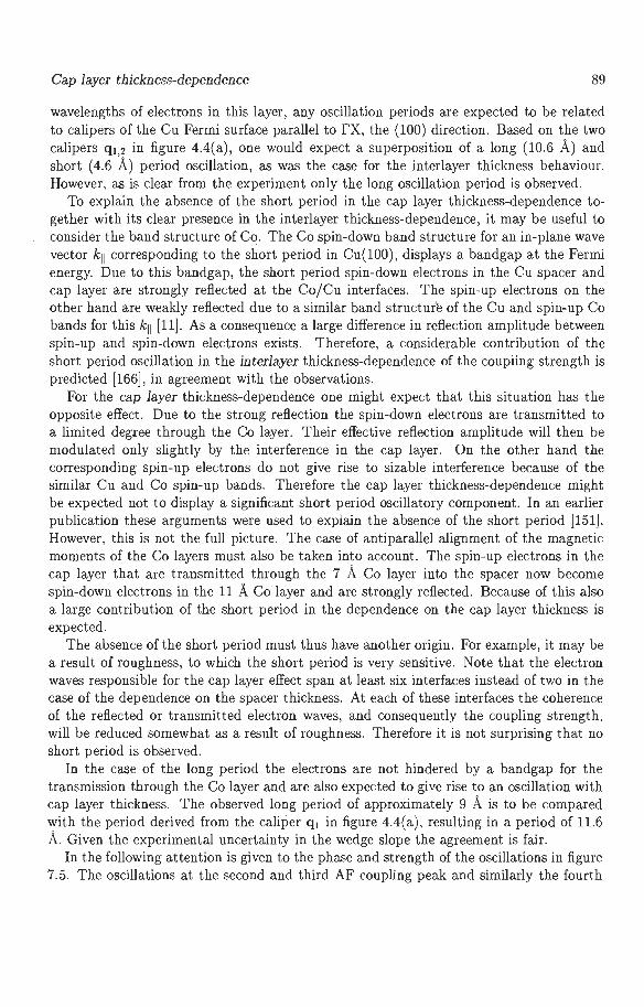
Cap layer thickness-dependence 89
wavelengths of electrons in this layer, any oscillation periods are expected to be related to calipers of the Cu Fermi surface parallel to fX, the (100) direction. Based on the two calipers q1,2 in figure 4.4(a), one would expect a superposition of a long (10.6 A) and short ( 4.6 A) period oscillation, as was the case for the interlayer thickness behaviour. However, as is clear from the experiment only the long oscillation period is observed.
To explain the absence of the short period in the cap layer thickness-dependence together with its clear presence in the interlayer thickness-dependence, it may be useful to consider the band structure of Co. The Co spin-down band structure for an in-plane wave vector k11 corresponding to the short period in Cu(lOO), displays a bandgap at the Fermi energy. Due to this bandgap, the short period spin-down electrons in the Cu spacer and cap layer are strongly reflected at the Co/Cu interfaces. The spin-up electrons on the other hand are weakly reflected due to a similar band structur'e of the Cu and spin-up Co bands for this k11 [11] . As a consequence a large difference in reflection amplitude between spin-up and spin-down electrons exists. Therefore, a considerable contribution of the short period oscillation in the interlayer thickness-dependence of the coupling strength is predicted [166], in agreement with the observations.
For the cap layer thickness-dependence one might expect that this situation has the opposite effect. Due to the strong reflection the spin-down electrons are transmitted to a limited degree through the Co layer. Their effective reflection amplitude will then be modulated only slightly by the interference in the cap layer. On the other hand the corresponding spin-up electrons do not give rise to sizable interference because of the similar Cu and Co spin-up bands. Therefore the cap layer thickness-dependence might be expected not to display a significant short period oscillatory component. In an earlier publication these arguments were used to explain the absence of the short period [151]. However, this is not the full picture. The case of antiparallel alignment of the magnetic moments of the Co layers must also be taken into account. The spin-up electrons in the cap layer that are transmitted through the 7 A Co layer into the spacer now become spin-down electrons in the 11 A Co layer and are strongly reflected. Because of this also a large contribution of the short period in the dependence on the cap layer thickness is expected.
The absence of the short period must thus have another origin. For example, it may be a result of roughness, to which the short period is very sensitive. Note that the electron waves responsible for the cap layer effect span at least six interfaces instead of two in the case of the dependence on the spacer thickness. At each of these interfaces the coherence of the reflected or transmitted electron waves, and consequently the coupling strength, will be reduced somewhat as a result of roughness. Therefore it is not surprising that no short period is observed.
In the case of the long period the electrons are not hindered by a bandgap for the transmission through the Co layer and are also expected to give rise to an oscillation with cap layer thickness. The observed long period of approximately 9 A is to be compared with the period derived from the caliper q 1 in figure 4.4(a), resulting in a period of 11.6 A. Given the experimental uncertainty in the wedge slope the agreement is fair.
In the following attention is given to the phase and strength of the oscillations in figure 7.5. The oscillations at the second and third AF coupling peak and similarly the fourth
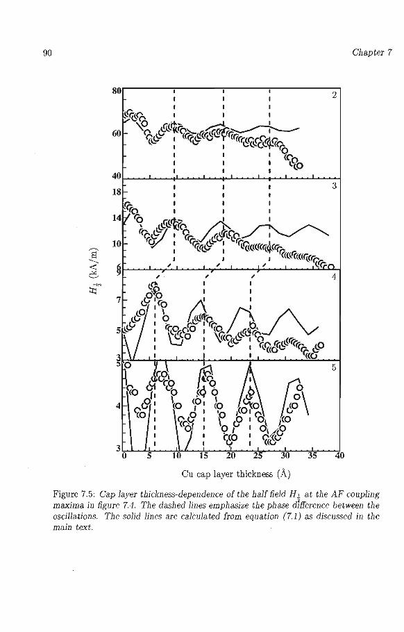
90 Chapter 7
80 2
Cu cap layer thickness (A)
Figure 7.5: Cap layer thickness-dependence of the half field Hi at the AF coupling maxima in figure 7.4. The dashed lines emphasize the phase d1fference between the oscillations. The solid lines are calCulated from equation (7.1) as discussed in the main text.
Cap layer thickness-dependence 91
and fifth AF peak have approximately the same phase, whereas the oscillations at the second and third AF peak have nearly opposite phases compared to the oscillations at the fourth and fifth AF peak. For clarity this is emphasized by the dashed lines in figure 7.5. Furthermore, it appears that for the AF peaks at larger interlayer thickness the absolute amplitude of the oscillations is smaller and the decay of the amplitude is slower.
To provide a mathematical understanding for the above observations, an approximate equation for the bilinear coupling strength J1 is derived. The procedure is to calculate the effective reflection coefficients for a given potential using equation (2.42) and to substitute these into equation (2.38) for n = 1. Within the free electron approximation, in the limit of large interlayer, magnetic layer and cap layer thickness and for small r ""'" one obtains:
J, '.:::'. _1_ .!:!_Im~ [r2 ( D )-2 e2ikFD 47r2 2m 2 00 kF
-2r2 (1 _ r2 ) ( D + .£)-2 e2ikFD+2ik~L
00 00 k k! F F
+r~(l _ 2r~) ( D + ~ + !_)-2 e2ikFD+2ik~L+2ikFT
kF kF kF
-r2 ( D + .£ + I._)-2 e2ikFD+2ikFL+2ikFT]
00 kF kF kF (7.1)
For brevity only the relevant terms are shown. Here, the simplified one-dimensional potential given in figure 7.6 is used. D, L and T are the interlayer, magnetic layer and cap layer thickness, respectively. Only two potential levels have been assumed so that two wave vectors and one reflection coefficient r 00 = ( kF - k~) / ( kF + k~) enter the equation. Electrons of both spin directions in Cu and spin-up electrons in Co have Fermi wave vector kF; spin-down electrons in Co and electrons of both spin types in the Au layer have Fermi wave vector k~. The first two terms in equation (7.1) represent the interlayer and magnetic layer thickness-dependence and may be recognized as precisely the terms making up equation (2.49) in section 2.9. The last two terms express an oscillation of the coupling strength with the cap layer thickness. The free electron approximation itself is · expected to describe the present experiment fairly well since for the long period oscillation in Co/Cu(lOO) the free electron-like s,p bands make the dominant contribution.
Quite remarkably the various terms in equation (7.1) may be obtained by considering the various closed paths of electron waves. This will be demonstrated below but first the method is clarified. On their way the electron waves are reflected at or transmitted through the interfaces with certain reflection and transmission amplitudes and propagate through the layers thereby acquiring a phase. Furthermore, the integration over all wave vectors in the Fermi sphere gives rise to a quadratic decay with the total thickness of all layers accessed, where each layer thickness is weighted by the relevant Fermi wave vector. An attempt is made to answer the important question of how these closed paths of electron waves are related to the coupling strength. In section 2.4 it has been argued that Green's functions and transfer matrices represent travelling waves and reflections at perturbation potentials. Equation (2.28) therefore represents all travelling and multiply reflecting electron waves within the potential landscape of the magnetic multilayer. The
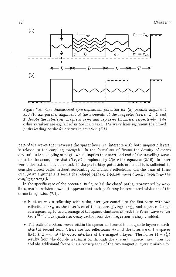
92 Chapter 7
(a)
rT = 0 kF r 1 = r 00
--------~----------------------
+--- L -•llli414-- D --•llli414- L -•llli414,___ T -+ (b)
-----~ Figure 7.6: One-dimensional spin-dependent potential for (a) parallel alignment and (b) antiparallel alignment of the moments of the magnetic layers. D, L and T denote the interlayer, magnetic layer and cap layer thickness, respectively. The other variables are explained in the main text. The wavy lines represent the closed paths leading to the four terms in equation (7.1).
part of the waves that traverses the spacer layer, i.e. interacts with both magnetic layers , is related to the coupling strength. In the formalism of Bruno the density of states determines the coupling strength which implies that start and end of the travelling waves must be the same, note that G(x, x') is replaced by G(x, x) in equation (2.16). In other words the paths must be closed. If the perturbing potentials are small it is sufficient to consider closed paths without accounting for multiple reflections. On the basis of these qualitative arguments it seems that closed paths of electron waves directly determine the coupling strength.
In the specific case of the potential in figure 7.6 the closed paths, represented by wavy lines, can be written down. It appears that each path may be associated with one of the terms in equation (7.1).
• Electron waves reflecting within the interlayer contribute the first term with two reflections +r = at the interfaces of the spacer, giving: +r;,, and a phase change corresponding to two crossings of the spacer thickness D with the Fermi wave vector kp: e2
ikFD . The quadratic decay factor from the integration is simply added.
• The path of electron waves within the spacer and one of the magnetic layers contributes the second term . There are two reflections: +r 00 at the interface of the spacer layer and -r00 at the outer interface of the magnetic layer. The factor (1 - r;,) results from the double transmission through the spacer/magnetic layer interface and the additional factor 2 is a consequence of the two magnetic layers available for
Cap layer thickness-dependence 93
two different interference paths. The overal prefactor now becomes: -2r~(l - r~). For this term the phase factor and the quadratic decay factor contain both D and L.
• Similarly, the third term results from the path through the spacer, magnetic and cap layer, where the fourfould transmission (1- r~)2 is approximated by (1- 2r.;,). Note that k~ must be taken for the magnetic layer.
• Finally, the fourth term results from the antiferromagnetic configuration. Note that by reversing the magnetization of the right magnetic layer the spin-up and down potentials are interchanged in that layer, figure 7.6(b). Due to the subtraction of ferro- and antiferromagnetic energy contributions the fourth term has an extra minus sign. The wave vector in the magnetic layer is now kF.
Although, all terms in equation (7.1) are obtained by looking for closed paths of travelling electron waves, it is emphasized that no proof is given for the correctness of this interpretation of equation (7.1).
Returning to a discussion of the consequences of equation (7.1) in relation to the experiment, one should note that the prefactors of the cap layer terms reveal that the amplitude of the cap layer oscillation is larger for thinner magnetic layers and interlayers. This is the reason why the magnetic layer thickness should be small, and why the amplitude of the oscillation decreases with increasing interlayer thickness. In addition, this factor shows why the decay of the oscillation with the cap layer thickness is slower for the AF maxima at larger interlayer thickness. A larger D reduces the decay effect of T. A further point concerns the relative phase of the oscillations in figure 7.5. The phase factor in the cap layer terms of equation (7.1) is determined by D and L, where Lis constant. Since the difference in interlayer thickness between the second and third (and also the fourth and fifth) AF coupling peak equals one long oscillation period, the corresponding oscillations are phase shifted one period. This obviously appears as no phase shift at alL The oscillations at e.g. the third and fourth AF coupling peak have nearly opposite phases because the interlayer thicknesses differ one short period which is accidentally approximately half a long period. ·
The quantitative agreement of the model with the data is illustrated by the solid lines in figure 7.5 which are calculated from the last two terms of equation (7.1). As the offset determined by the first two terms of equation (7.1) does not include the short period contribution, the height of the peaks in figure 7.4 has been substituted. kF = 1.471 A-1
,
k~ = 1.261 A- 1 as in [48], L = 7 A and the position of the peaks in figure 7.4 for D, have been substituted. The period determined by kF is 11.6 A whereas the experimental period is 9.0 A. In assuming that the latter is due to an incorrect wedge slope the result has been scaled by 1
9j 06 on the horizontal axis. In addition, an overall reduction factor (4),
due to elevated temperatures and sample imperfections like interface roughness [163] is applied to the vertical axis. This reduction factor is estimated in the following way. From the fit of the interlayer thickness-dependence, shown by the solid line in figure 7.4, one learns that the long and short period oscillation have approximately the same amplitude. Therefore it is assumed that the coupling strength at the second AF peak ( J = -0.075 mJ/m2) can be split-up in two equal contributions of (-0.0375 mJ/m2 ) of the long and
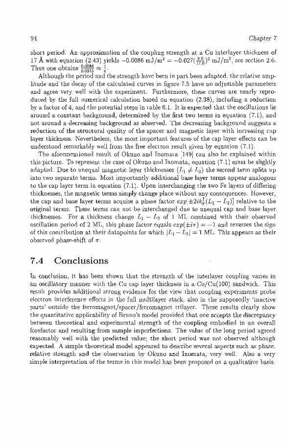
94 Chapter 7
short period. An approximation of the coupling strength at a Cu interlayer thickness of 17 A with equation (2.43) yields -0.0086 mJ/m2 = -0.027( 1
97°0 ) 2 mJ/m2, see section 2.6.
Thus one obtains ~:~~~~ ~ ~· Although the period and the strength have been in part been adapted, the relative amp
litude and the decay of the calculated curves in figure 7.5 have no adjustable parameters and agree very well with the experiment. Furthermore, these curves are nearly reproduced by the full numerical calculation based on equation (2.38) , including a reduction by a factor of 4, and the potential steps in table 6.1. It is expected that the oscillations lie around a constant background , determined by the first two terms in equation (7.1), and not around a decreasing background as observed. The decreasing background suggests a reduction of the structural quality of the spacer and magnetic layer with increasing cap layer thickness. Nevertheless, the most important features of the cap layer effects can be understood remarkably well from the free electron result given by equation (7.1).
The aforementioned result of Okuno and Inomata [149] can also be explained within this picture. To represent the case of Okuno and Inomata, equation (7.1) must be slightly adapted. Due to unequal magnetic layer thicknesses (L1 -j. L2 ) the second term splits up into two separate terms. Most importantly additional base layer terms appear analogous to the cap layer term in equation (7.1). Upon interchanging the two Fe layers of differing thicknesses , the magnetic terms simply change place without any consequences. However, the cap and base layer terms acquire a phase factor exp[±2iki(L1 - L2 )] relative to the original terms. These terms can not be interchanged due to unequal cap and base layer thicknesses. For a thickness change L 1 - L2 of 1 ML combined with their observed oscillation period of 2 ML, this phase factor equals exp( ±i1r) = -1 and reverses the sign of this contribution at their datapoints for which IL1 - £ 2 1 = 1 ML. This appears as their observed phase-shift of 1r.
7 .4 Conclusions
In conclusion, it has been shown that the strength of the interlayer coupling varies in an oscillatory manner with the Cu cap layer thickness in a Co/Cu(lOO) sandwich. This result provides additional strong evidence for the view that coupling experiments probe electron interference effects in the full multilayer stack, also in the supposedly 'inactive parts' outside the ferromagnet/spacer/ferromagnet trilayer. These results clearly show the quantitative applicability of Bruno's model provided that one accepts the discrepancy between theoretical and experimental strength of the coupling embodied in an overall forefactor and resulting from sample imperfections. The value of the long period agreed reasonably well with the predicted value; the short period was not observed although expected . A simple theoretical model appeared to describe several aspects such as phase, relative strength and the observation by Okuno and Inomata, very well. Also a very simple interpretation of the terms in this model has been proposed on a qualitative basis.
Chapter 8
Importance of matching Fermi surfaces
Abstract1
Not all calipers are candidate for the oscillation periods, they are subject to certain selection rules. The in-plane wave vector of the caliper of the spacer and any other layer must be conserved due to the in-plane translational invariance. In this chapter an experiment that studies the selection rules for calipers of the Cu and Ni Fermi surfaces is described. Although for Cu and Ni an exact match of the in-plane wave vector of the calipers is not expected for the short period, a short period oscillation as a function of the Ni thickness bas nevertheless been observed. Several arguments have been given that allow for small differences, as is the case for Cu and Ni Fermi surfaces.
8.1 Introduction and motivation
Many aspects of the oscillatory interlayer exchange coupling in magnetic multilayers are well understood by now [185, 186]. Initially, the period of the oscillation of the coupling between two ferromagnetic layers as a function of the thickness of the spacer was shown to be determined by extremal spanning vectors, calipers, of the spacer Fermi surface (FS). Later, an oscillatory dependence on the thickness of the ferromagnetic [114, 148, 149] and cap layers [151, 153, 154] has been observed, see also chapters 6 and 7. In these cases the oscillation periods are also related to calipers of the FS, more precisely, the FS of the layers that are varied in thickness. These experiments support theories that predict that spin-dependent reflection of electron waves in the whole multilayer stack determines the coupling [48, 51]. They also raised the question as to which of the calipers of the FS of the ferromagnet or cap layer material. determines the period. For example, the minority spin FS of fee Co alone has ten different calipers along the (100) direction, which are all potential candidates for defining oscillation periods [114]. However, selection rules limit the choice. Due to the in-plane translation symmetry of the multilayers the in-plane wave
1Parts of this chapter have been published in Phys. Rev. B. 54 748 (1996)
95
96 Chapter 8
vector k11
must be conserved for calipers of the spacer FS and the FS of the ferromagnet or cap layer material [187].
So far, all experiments automatically obeyed this selection rule due to the fact that at k 11 = 0 A-1 the FSs usually have calipers for reasons of symmetry [114, 149, 151, 154] or because identical spacer and cap layer materials ensure a perfect match of the FSs [153]. In the case of Cu and Ni FSs also a perfect match exists for the calipers at k11 = 0 A- 1 (responsible for a long period oscillation), but for the calipers at k
11 # 0 A- 1 (short
period) the k11
likely differ. Therefore, a study of the dependence of the coupling across a Cu interlayer as a function of a ferromagnetic Ni layer may or may not reveal a short period oscillation and shed some light on the underlying selection rules.
8.2 Experimental
To measure the dependence of the coupling on the Ni thickness, the following multilayer was deposited by Molecular Beam Epitaxy (!VIBE) on a Cu(lOO) single crystal:
Cu(l00)/40 A Co/Cu wedge (0-35 A)/ 4 A Co/Ni wedge (0-25 A)/30 A Co/10 A Cu/20 A Au.
The sample composition is very similar to the one discussed in chapter 6. In that case the dependence on the Co layer thickness was studied requiring Co wedges, whereas here, to study the dependence on the Ni layer thickness, a Ni wedge is employed. Arguments for the specific sample composition in chapter 6 in relation to the measurement of the coupling also apply here. For example the 30 A Co layer on top of the Ni wedge serves as a magnetic grip to facilitate the measurement of Kerr hysteresis loops at small Ni thicknesses where the effects are expected to be largest. Furthermore, it contributes to the magnetic anisotropy resulting in a hysteresis loop from which the coupling strength can be determined more accurately. To allow independent variation of the Cu and Ni thickness the wedges were arranged perpendicularly. However, in contrast to the sample in chapter 6, here a sample with asymmetric magnetic layers, i.e. with one single Ni wedge, has been used. In the case of symmetric magnetic layers, i.e. two Ni wedges, the inevitable inequality of the wedge slopes and starting points can obscure the oscillatory behaviour [147]. A thin Co layer was inserted between the Cu and Ni wedges as the exchange coupling in Co/Cu/Co is larger than in Co/Cu/Ni and can be measured more precisely. In addition, it is well-known that Ni in contact with Cu results in a so-called magnetically dead layer at the Cu/Ni interface and consequently a modified Ni FS [188]. The combined result of the SAM and the vibrating crystal wedge analysis yielded a Cu wedge slope of 4.2 ± 0.6 A/mm and a Ni wedge slope of 3.2 ± 0.5 A/mm.
8.3 Results and discussion
First the dependence of the coupling strength on the interlayer thickness has been studied at different Ni layer thicknesses to locate antiferromagnetic (AF) coupling peaks and to trace their position with changing thickness of the Ni layer. Examples of Kerr hysteresis loops for various AF coupling strengths are shown in figure 8.1. A plot of the half field
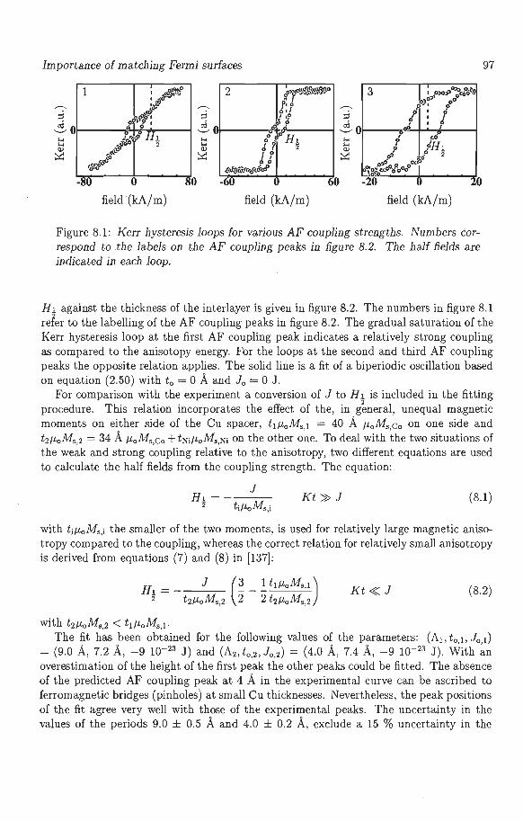
Importance of matching Fermi surfaces
1
0
field (kA/m)
Figure 8.1 : Kerr hysteresis loops for various AF coupling strengths. Numbers correspond to the labels on the AF coupling peaks in figure 8.2. The half fields are indicated in each loop.
97
H1 against the thickness of the interlayer is given in figure 8.2. The numbers in figure 8.1 refer to the labelling of the AF coupling peaks in figure 8.2. The gradual saturation of the Kerr hysteresis loop at the first AF coupling peak indicates a relatively strong coupling as compared to the anisotopy energy. For the loops at the second and third AF coupling peaks the opposite relation applies. The solid line is a fit of a biperiodic oscillation based on equation (2.50) with t0 = 0 A and J0 = 0 J.
For comparison with the experiment a conversion of J to H l is included in the fitting 2
procedure. This relation incorporates the effect of the, in general , unequal magnetic moments on either side of the Cu spacer, t 1µ 0 Ms,I = 40 A µ0Ms,Co on one side and t2µ0Ms,2 = 34 A µoMs,Co + tNiµoMs,Ni on the other one. To deal with the two sit uations of the weak and strong coupling relative to the anisotropy, two different equations are used to calculate the half fields from the coupling strength. The equation:
Hi= 2
J Kt» J (8.1)
with t;µ 0 Ms,i the smaller of the two moments, is used for relatively large magnetic anisotropy compared to the coupling, whereas the correct relation for relatively small anisotropy is derived from equations (7) and (8) in [137]:
Hi=_ J (~ _ ~ t1µ0Ms,1) 2 t2µoMs,2 2 2 t2µoMs,2
Kt« J (8.2)
with t2µ0Ms,2 < t1µ0Ms,1 · The fit has been obtained for the following values of the parameters: (A1 , t 0 , 1 , J0 , 1)
= (9.0 A, 7.2 A, -9 10-23 J) and (A2 , t 0,2, J0 ,2) = (4.0 A, 7.4 A, -9 10-23 J). With an overestimation of the height of the first peak the other peaks could be fitted. The absence of the predicted AF coupling peak at 4 A in the experimental curve can be ascribed to ferromagnetic bridges (pinholes) at small Cu thicknesses. Nevertheless, the peak positions of the fit agree very well with those of the experimental peaks. The uncertainty in the values of the periods 9.0 ± 0.5 A and 4.0 ± 0.2 A, exclude a 15 % uncertainty in the

98
30
20
10
0
0
1 0
Cu thickness (A)
Chapter 8
40
Figure 8.2: Dependence of the half field H 1 on the thickness of the Cu interlayer 2
at zero Ni thickness. The solid line is a fit based on the phenomenological equation (2.50) . Numbers label the AF coupling peaks.
wedge slope. Comparison with the theoretical periods of 10.6 A and 4.6 A [163], shows that the ratio of the periods is correct but the absolute values are too low. This indicates that the actual wedge slope is probably somewhat larger than the measured one, but still lies within the limits set by the experimental accuracy. For the following, however, it is sufficient to note that two oscillation periods are observed.
At interlayer thicknesses corresponding to the AF coupling peaks labelled 1 and 2 in figure 8.2, Kerr loops were measured as a function of the thickness of the Ni layer. To be sure to find the maximum AF coupling at each Ni thickness, a series of 9 Kerr loops was measured as a function of the Cu thickness across each AF coupling peak at positions separated by 0.05 mm (0.2 A Cu), thus approximately spanning the full width at half maximum of the AF peaks in figure 8.2. However , instead of the maximum AF coupling the sum of the half fields obtained from the 9 loops is considered, in order to reduce noise. In figure 8.3 the summed AF half fields are plotted as a function of the Ni layer thickness at the first two interlayer AF maxima. A significant variation is seen . According to coupling theories an oscillatory behaviour is expected with an oscillatory contribution for each caliper of the Ni FS, the k11 of which conicides with that of a caliper of the Cu FS.
It is clear that the observed variation can not be characterized by a single, period. Investigation of the Ni FS shows that three calipers, hence three oscillation periods may appear. Two periods a long and short period are obtained from the spin-down Ni FS , which resembles that of Cu. In addition, one long period oscillation is derived from the spin-up Ni FS. However, the spin-down long period is expected to dominate the spin-up long period due to a larger potential step with a stronger reflection. Therefore, a fit with two periods is attempted using equation (2.50). The extra J0 offset accounts for
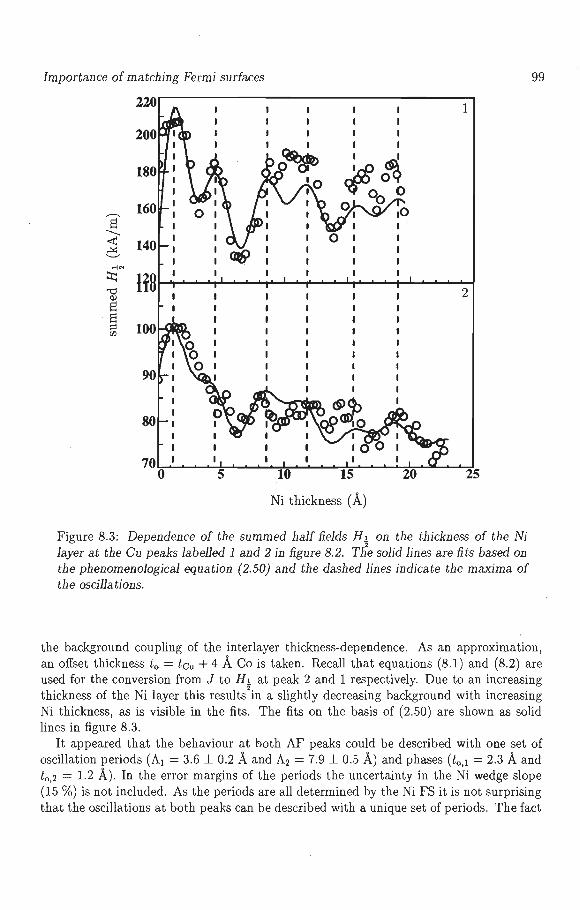
Importance of matching Fermi surfaces
1
s 160 .....__ -< 140 ~ '--'
_,.,.. ::i::: HB -0 Q) 2 s s ;::l 100 en
90
80
70..,,..... ................... ~ .................................................... .....,..=-"'"-'-_._.....,...,......_...._ ......... ......,. 0 5 10 15 20 25
Ni thickness (A)
Figure 8.3: Dependence of the summed half fields H 1 on the thickness of the Ni 2
layer at the Cu peaks labelled 1 and 2 in figure 8.2. The solid lines are fits based on the phenomenological equation (2.50) and the dashed lines indicate the maxima of the oscillations.
99
the background coupling of the interlayer thickness-dependence. As an approximation, an offset thickness t0 = tcu + 4 A Co is taken. Recall that equations (8.1) and (8.2) are used for the conversion from J to H 1 at peak 2 and 1 respectively. Due to an increasing
2 thickness of the Ni layer this results in a slightly decreasing background with increasing Ni thickness, as is visible in the fits. The fits on the basis of (2.50) are shown as solid lines in figure 8.3.
It appeared that the behaviour at both AF peaks could be described with one set of oscillation periods (A1 = 3.6 ± 0.2 A and A2 = 7.9 ± 0.5 A) and phases (t0 , 1 = 2.3 A and t0 ,2 = 1.2 A) . In the error margins of the periods the uncertainty in the Ni wedge slope (15 %) is not included. As the periods are all determined by the Ni FS it is not surprising that the oscillations at both peaks can be described with a unique set of periods. The fact
100 Chapter 8
that the phases of the oscillations do not depend on the Cu thickness is a coincidence and can be explained along similar lines as in chapter 7. By substituting the Ni thickness for the cap layer thickness in equation (7. l) this becomes clear. The phase of the oscillations as a function of the Ni thickness is determined by the Cu spacer thickness. Between peak 1 and 2 in figure 8.2 the phase difference is approximately a multiple of 27r for both the short and long period. Therefore, it appears that there is no phase shift at all between oscillations 1 and 2 in figure 8.3.
The fits do not match the data in the whole thickness range. In addition to the omitted discretization as discussed in section 2.10, this is perhaps a consequence of the summing procedure. Nevertheless, the positions of the maxima and minima are reproduced well. Several modifications of equation (2.50), such as weighting the thicknesses with the Fermi vectors in the prefactors as in equations (2.49) and (7.1) , may improve the fits. However , the periods, which are the main concern of this experiment, will be unaffected by such modifications.
To relate the experimentally observed periods to calipers of the spin-up or spin-down FS of Ni , the relevant literature values of the latter are summarized in table 8.1. For comparison also the results of self-consistent Augmented Spherical Wave (ASW) calculations in the Local Density Approximation are listed in table 8.1 1 . From the calculated Ni FSs the calipers and the corresponding aliased periods could be derived by measuring their length along rx. As is clear from the table the long period ranges from 6.7 A to 8.3 A for spin-up electrons and from 7.4 A to 8.9 A for spin-down electrons. Much better agreement is found between calculations of the caliper of the spin-up Ni FS that is responsible for a short period of 3.6 to 3.7 A. However, the corresponding in-plane wave vector k11 of the short period ranges from 0.50fK to 0.57fK. No caliper giving rise to a short period exists for spin-down electrons. The fact that the variation of the value for the long period is considerably larger than that for the short period is a result of the aliasing process making the long period more susceptible to slight changes in the length of the caliper, see equation (2.44).
On comparing the experimental value of the long period (7.9 ± 1.5 A) with the values in table 8.1, it appears that the long period may stem from the caliper of either the spinup (6.7-8.3 A) or the spin-down FS (7.4-8.9 A). From the theoretical point of view the preferred spin direction seems to be spin-down. In the free electron approximation which is approximately valid for the electrons responsible for the long period, the height of the potential steps, and therefore the reflection, at the Cu/Co, Co/Ni and Ni/Co interfaces is larger for spin-down. electrons, see table 6.1. For this reason spin-down electrons are expected to dictate the coupling. However, if multiple reflections are taken into account a complication arises as a result of destructive and constructive interferences in the 4 A Co layer which can promote a certain spin direction. For the short period a caliper of the Ni FS only exists for spin-up electrons and the spin direction is clear. Indeed the theoretical value for spin-up electrons (3.6-3.7 A) agrees very well with the fitted value (3.6 ± 0.7 A). . .
In relation to the question of the conservation of k 11 the following is noted. For reasons of symmetry at k11 = 0 A -I calipers of the FS always exist if the direction perpendicular to
1The ASW calculations have been performed by prof. dr . R. Coehoorn.
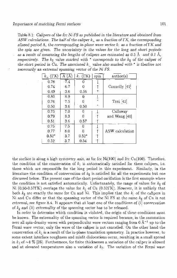
Importance of matching Fermi surfaces 101
Table 8.1: Calipers of the fee Ni FS as published in the literature and obtained from ASW calculations. The half of the caliper k.L as a fraction of r X , the corresponding aliased period A, the corresponding in-plane wave vector k11 as a fraction offK and the spin are given. The uncertainty in the values for the long and short periods as a result of measuring the lengths of calipers are estimated as 0.5 A and 0.1 A, respectively. The k11 value marked with • corresponds to the k11 of the caliper of the short period in Cu. The associated k.L value also marked with • is therfore not necessarily an extremal spanning vector of the Ni FS.
I k.L (rX) I A (A) I k 11 (rK) I spin I author(s)
0.76 7.4 0 l 0.74 6.7 0 T Connolly [ 41] 0.49 3.6 0.56 T 0.80 8.9 0 l 0.76 7.5 0 T Tsui [42] 0.50 3.6 0.50 T 0.75 7.0 0 l Callaway 0.79 8.3 0 T and Wang [40] 0.51 3.6 0.57 T 0.75 7.5 0 l 0.77 8.0 0 T ASW calculation 0.52* 3.7 0.52* T 0.52 3.7 0.54 T
the surface is along a high symmetry axis, as for fee Ni(lOO) and fee Cu(IOO). Therefore, the condition of the conservation of k11 is automatically satisfied for these calipers, i.e. those which are responsible for the long period in this experiment. Similarly, in the literature the condition of conservation of k11 is satisfied for all the experiments but one discussed below. The present case of the short period oscillation is the first example where the condition is not satisfied automatically. Unfortunately, the range of values for k11 of Ni (0.50-0.57fK) overlaps the value for k11 of Cu (0.52fK). However, it is unlikely that both k11 are exactly the same for Cu and Ni. This implies that the k11 of the calipers in Ni and Cu differ or that the spanning vector of the Ni FS at the same k 11 of Cu is not extremal, see figure 8.4. It appears that at least one of the conditions of (i) conservation of k11 and (ii) extremality of the spanning vector has to be released.
In order to determine which condition is violated, the origin of these conditions must be known. The extremality of the spanning vector is required because, in the summation over all spin-density waves with perpendicular wave vectors ranging from 0 A- 1 up to the Fermi wave vector, only the wave of the caliper is not cancelled. On the other hand the conservation of k11 is a result of the in-plane translation symmetry. In practice however, to some extent interface roughness and misfit dislocations occur, resulting in a small spread in k11 of ""'1 % [25]. Furthermore, for finite thicknesses a variation of the caliper is allowed and at elevated temperatures also a variation of k11 . The variation of the Fermi wave
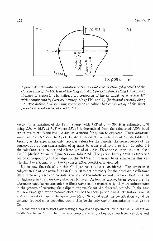
102 Chapter 8
Cu t fK [011] k11 Ni
k_L,short Ml------~ 00
't1-. 't1-.
rx [100] k_1_ -+
Figure 8.4: Schematic representation of the relevant cross section ('dogbone') of the Cu and spin-up Ni FS. Half of the long and short period calipers along fX is shown (horizontal arrows). The calipers are composed of the extermal wave vectors k± with components k11 (vertical arrows), along rK, and k_1_ (horizontal arrows), along rx. The dashed half spanning vector is not a caliper but conserves k 11 of the short period extremal vector of the Cu FS.
vector for a variation of the Fermi energy with k8 T at T = 300 K is estimated 1 % using l:!.kp = (dE/dk)k8 T where dE/dk is determined from the calculated ASW band structures at the Fermi level. A similar variation for k11 can be expected. These variations would almost reconcile the k 11 of the short period of Cu with that of Ni, see table 8.1. Finally, as the experiment only provides values for the periods, the consequences of the conservation or non-conservation of k11 must be translated into a period. In table 8.1 the calculated non-caliper and related period of the Ni FS at the k 11 of the caliper of the Cu FS (dashed arrow in figure 8.4) are tabulated. The period hardly deviates from the period corresponding to the caliper of the Ni FS and it can not be established in this way whether the extremality or the k11 conservation condition is violated.
Up to now the role of the thin Co layer has not been considered . The presence of calipers in Co at the same k11 as in Cu or Ni is not necessary for the observed oscillations [187] . One only needs to consider the FSs of the interlayer and the layer that is varied in thickness , in this case the embedded Ni layer. As long as further layers separating the aforementioned layers transmit the Bloch waves at the respective k 11 , they are unimportant in the process of selecting the calipers responsible for the observed periods. In the case of Co a band gap for spin-down electrons of the short period exists. Therefore, even if a short period caliper in the spin-down FS of Ni would exist, its contribution would be strongly reduced since tunneling would then be the only way of transmission through the Co.
In this respect it is worth addressing a cap layer experiment, as in chapter 7, where an oscillatory behaviour of the interlayer coupling as a function of a cap layer was observed

Importance of matching Fermi surfaces 103
in Fe/ Au/Fe/ Au(lOO) [153]. In this experiment a short period oscillation resulting from a caliper at the neck of the Au FS with kn f:. 0 A-1 appeared. Similar to the Co layer in this experiment, the role of the Fe layer is merely to transmit the spin-density waves and its FS does not play a role in the selection of calipers of the Au FS. Therefore, the conditions of the conservation of kn and of the extremality of the spanning vectors at the same k11 are, of course, satisfied if the interlayer and cap layer are made of the same material. The cap layer type experiments can be modified to further investigate the question of conservation of kn by choosing cap layer materials that differ from the interlayer material, e.g. Fe/ Au/Fe/ Ag.
8.4 Conclusions
A biperiodic oscillatory behaviour of the coupling strength with the thickness of an embedded Ni layer has been observed. The observed long and short periods can be related to calipers of the Ni FS. Although it could not be made conclusive due to uncertainties in both experimental and theoretical values, it is not expected that the calipers of the Cu and Ni FS share the same kn in the case of the short period. Therefore the observation of a short period oscillation of the coupling across Cu as a function of the Ni thickness implies that in practice the requirement of the conservation of k11 or of the extremality of the spanning vector of the FS are not that strict.
Moreover, the experiment extends the study of the dependence of the coupling on the ferromagnetic layer thickness for the magnetic transition metals, so far only Co and Fe were studied [114, 148, 149], and confirms that layers that are not adjacent to the spacer also contribute to the coupling strength.
104 Chapter 8
Chapter 9
Interlayer coupling across 'semiconductors'
Abstract1
The structure and the interlayer exchange coupling in MBE-grown, nominal Fe/Ge1_xFex/Fe (x=O.O, 0.25, 0.33, 0.5) and Fe/Si/Fe sandwiches with wedgeshaped spacer layers are investigated. In the case of Fe/Si also a sample with a wedge-shaped magnetic layer is studied. From structural analysis with LEED and from magnetic analysis with the magneto-optical Kerr effect, it is concluded that the Si spacer transforms into a SiFe alloy (probably metallic Si0.5Feo.s) with the deposition of Fe. A strong antiferromagnetic (AF) coupling is found in the case of Fe/Si, but no AF coupling is found for Fe/Ge1_xFex. It appears that the interlayer exchange coupling in Fe/Si(SiFe)/Fe sandwiches decreases monotonically with increasing spacer thickness instead of oscillatory. Shi et al. predict such behaviour for Si0.5Fe0.5 having the CsCl-structure. They argue that this is a result of a high density of states above but close to the Fermi level. In terms of the Bruno model the behaviour originates from an imaginary caliper.
9.1 Introduction and motivation
Up to now only the coupling across metallic spacers has been discussed, but what about coupling across semiconducting or insulating spacers? Apart from a fundamental motivation, this property is also interesting from the point of view of applications. Before we try to answer the above question in the following sections, these applications are discussed first.
A major difference between a semiconductor or an insulator and a metal is the much smaller conductivity or likewise the larger resistance. This is advantageous for a GMR magnetoresistive field sensor where the current flows perpendicular to the plane of a magnetic/non-magnetic multilayer. Metallic prototypes of these sensors suffer from a
1Parts of this chapter will be published in J. Magn. Magn. Mater.
105
106 Chapter 9
very low resistance and must be lithographically structured into pillars with a small area [189-191] or contacted with superconducting leads [192-194] to be able to measure the magnetoresistance. A much higher resistance and hence a lower power consumption would result for semiconducting or insulating spacers compared to metallic ones. Note that the resistance of a thin insulator is not infinitely large due to tunnelling. AF interlayer exchange coupling across such spacers would provide a means to correctly align the moments of successive layers in the multilayer, see also section 1.
A second application relies on the possibility that the coupling strength can be increased by heating the spacer layer, see section 2.11, or in the case of a semiconducting spacer perhaps by illuminating it. This would be explained by an increase of the tunnelling probability through the insulator due to thermal or optical excitation. Via both mechanisms the coupling strength is increased. For example, the parallel alignment of the moments of two magnetic layers can be switched to antiparallel alignment by a heat or light pulse. This optical writing technique may be exploited in a magneto-optical storage disk.
Apart from a fundamental interest, these aspects initially motivated the study of the coupling across semiconductors such as Si and Ge.
9.2 Previous work
Due to its application potential, ferromagnet/semiconductor multilayers have received considerable interest over the last few years. Two early investigations of the coupling across Si reported the presence of ferromagnetic (F) coupling for small thicknesses (5-20 A) of Si [195, 196]. This can be a result of interface roughness and mixing, leading to F bridges through the Si (pinholes). In one study, however , hysteresis loops were shown that could be explained by AF coupling although another explanation was given by the authors [196].
Later, two groups identified AF coupling [197, 198] . Regarding the growth, both groups observed that Si and Fe form crystalline iron-silicide (SiFe) up to a certain nominal Si thickness 1 above which the spacer also contains amorphous Si (a-Si) . By using cooled substrates ( 40 K) the group of Landolt et al. [197] could limit the silicide formation to 11 A nominal Si . At larger Si thicknesses, hence partly across a-Si, F and AF coupling were mainly qualitatively measured in situ at 40 K on UHV evaporated Fe/Si/Fe sandwiches. An estimation of the coupling strength yielded -0.005 mJ /m 2. The group of Mattson et al. [198] observed rather strong AF coupling (-0.5 mJ /m 2) in Fe/Si multilayers with effectively crystalline SiFe spacers and deposited at room temperature by DC magnetron sputtering. In their case, a-Si growth started after deposition of more than 20 A nominal Si and coincided with the disappearance of the AF coupling.
Soon after the discovery of F and AF coupling, the observation of light-induced coupling across SiFe and SiO spacers has been claimed [101, 102, 199] . However, the long delay times of several seconds before the illumination took effect on the coupling, appeared to be inconsistent with the rapid excitation of electrons to the conduction band.
The dependence on the temperature has been investigated also. An increase of the F and AF coupling strength with increasing temperature was concluded for the Fe/Si
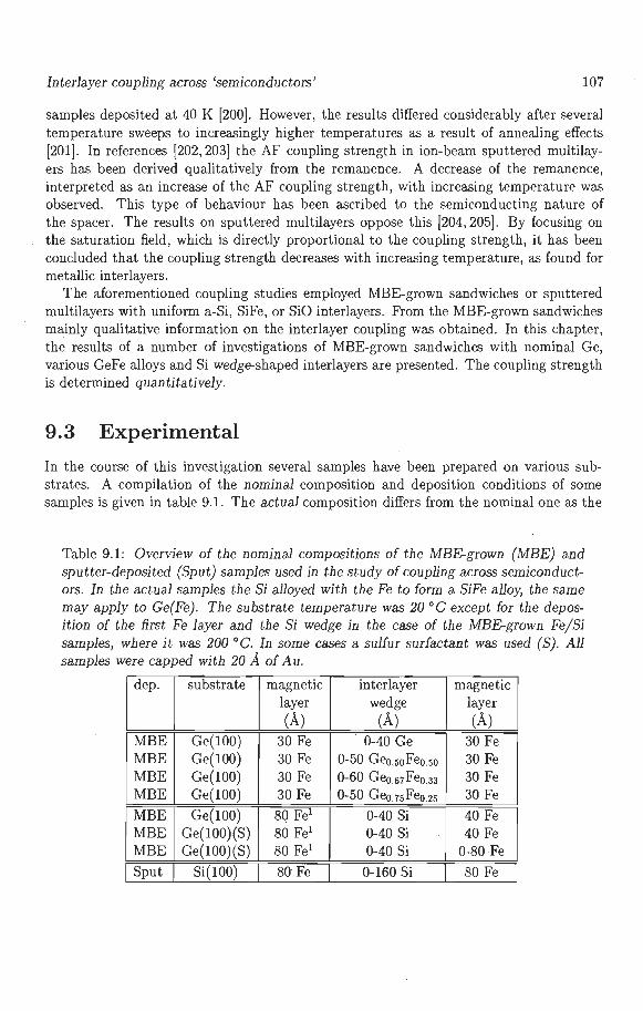
Interlayer coupling across 'semiconductors' 107
samples deposited at 40 K [200]. However, the results differed considerably after several temperature sweeps to increasingly higher temperatures as a result of annealing effects [201 ]. In references [202, 203] the AF coupling strength in ion-beam sputtered multilayers has been derived qualitatively from the remanence. A decrease of the remanence, interpreted as an increase of the AF coupling strength, with increasing temperature was observed. This type of behaviour has been ascribed to the semiconducting nature of the spacer. The results on sputtered multilayers oppose this [204, 205] . By focusing on the saturation field, which is directly proportional to the coupling strength, it has been concluded that the coupling strength decreases with increasing temperature, as found for metallic interlayers.
The aforementioned coupling studies employed MBE-grown sandwiches or sputtered multilayers with uniform a-Si, SiFe, or SiO interlayers. From the MBE-grown sandwiches mainly qualitative information on the interlayer coupling was obtained. In this chapter, the results of a number of investigations of MBE-grown sandwiches with nominal Ge, various GeFe alloys and Si wedge-shaped interlayers are presented. The coupling strength is determined quantitatively.
9. 3 Experimental
In the course of this investigation several samples have been prepared on various substrates. A compilation of the nominal composition and deposition conditions of some samples is given in table 9.1. The actual composition differs from the nominal one as the
Table 9.1: Overview of the nominal compositions of the MEE-grown (MEE) and sputter-deposited (Sput) samples used in the study of coupling across semiconductors. In the actual samples the Si alloyed with the Fe to form a SiFe alloy, the same may apply to Ge(Fe). The substrate temperature was 20 °C except for the deposition of the first Fe layer and the Si wedge in the case of the MEE-grown Fe/Si samples, where it was 200 °C. In some cases a sulfur surfactant was used (S). All samples were capped with 20 A of Au.
dep. substrate magnetic interlayer magnetic layer wedge layer (A) (A) (A)
MBE Ge(lOO) 30 Fe 0-40 Ge 30 Fe MBE Ge(lOO) 30 Fe 0-50 Geo.soFeo.so 30 Fe MBE Ge(lOO) 30 Fe 0-60 Geo.61 Feo.33 30 Fe MBE Ge(lOO) 30 Fe 0-50 Geo.1sFeo.2s 30 Fe
MBE Ge(lOO) 80 Fe1 0-40 Si 40 Fe MBE Ge(lOO)(S) 80 Fe1 0-40 Si 40 Fe MBE Ge(lOO)(S) 80 Fe1 0-40 Si 0-80 Fe
j Sput Si(lOO) 80' Fe 0-160 Si 80 Fe
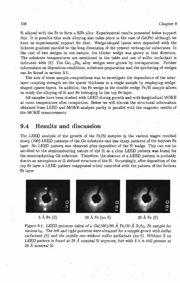
108 Chapter 9
Si alloyed with the Fe to form a SiFe alloy. Experimental results presented below support this. It is possible that such alloying also takes place in the case of Ge(Fe) although we have no experimental support for that. Wedge-shaped layers were deposited with the tickness gradient parallel to the long dimension of the present rectangular substrates. In the case of two wedges in one sample, the thicker wedge was grown in that direction . The substrate temperatures are mentioned in the table and use of sulfur surfactant is indicated with (S) . The Ge1_xFex alloy wedges were grown by coevaporation. Further information on deposition conditions, substrate preparation and the sputtering of wedges can be found in section 3.1.
The aim of these sample compositions was to investigate the dependence of the interlayer coupling strength on the spacer thickness in a single sample by employing wedgeshaped spacer layers. In addition, the Fe wedge in the double wedge Fe/Si sample allows to study the alloying of Si and Fe belonging to the top Fe layer.
All samples have been studied with LEED during growth and with longitudinal MOKE at room temperature after completion. Below we will discuss the structural information obtained from LEED and MOKE analysis partly in parallel with the magnetic results of the MOKE measurements.
9.4 Results and discussion
The LEED analysis of the growth of the Fe/Si samples in the various stages resulted sharp (100) LEED patterns of the Ge substrate and less sharp patterns of the bottom Fe layer. No LEED pattern was observed after deposition of the Si wedge. This can not be ascribed to the semiconducting nature of the Si as a clear LEED pattern was found for the semiconducting Ge substrate. Therefore, the absence of a LEED pattern is probably due to an amorphous or ill-defined structure of the Si. Surprisingly, after deposition of the top Fe layer a LEED pattern reappeared which coincided with the pattern of the bottom Fe layer
5 A Fe (S) 28 A Fe (no S) 28 A Fe (S)
Figure 9.1: LEED patterns taken of a Ge(l00)/80 A Fe/30 A Si/tFe Fe sample for various tFe · The left and right patterns were obtained for a sample grown with sulfur surfactant (S) and the middle one without sulfur surfactant (no S). Without S no LEED pattern is found at 28 A nominal Si anymore, but with Sit is still present at 28 A nominal Si.

Interlayer coupling across 'semiconductors' 109
The reappearance of the LEED suggests that the Si layer was transformed into a crystalline, epitaxial structure during the deposition of Fe. Such a crystallization due to diffusion of Fe into the Si has been proposed and supported earlier [101 , 206]. The crystallinity persisted up to 20 A nominal Si for the samples grown without sulfur surfactant, similar to sputtered Fe/Si samples in the literature [101, 206]. For the samples grown with sulfur surfactant this thickness range could be extended up to 28 A nominal Si thickness. This is shown in the LEED patterns in figure 9.1.
On the contrary, a weak LEED pattern was directly observed on the Ge1_xFex layer of the Fe/Ge1_xFex samples. The LEED pattern was similar to that of the bottom and top Fe layers indicating epitaxial growth.
In figure 9.2(a) a magneto-optical Kerr hysteresis loop measured at room temperature on the Fe/Ge/Fe sandwich is shown. The loop reveals that the magnetic layers are uncoupled or F coupled. As loops similar to the one in figure 9.2(a) are found when either the thickness of the spacer or its composition is varied, the same conclusion applies to the other Ge-based samples and other positions on the samples. According to Briner [207] a F coupling exists for Fe/Ge, however, its strength was not determined. From Kerr hysteresis loops on the present samples with two identical magnetic layers it is not possible to determine the F coupling strength, see section 2.2. Therefore, the remaining part of this chapter deals with Fe/Si samples.
From the Kerr hysteresis loop measured on the double wedge Fe/Si sample the presence of AF coupling is clear, see figure 9.2(b). For increasing magnitude of the magnetic field the alignment of the moments changes from antiparallel (AP) to parallel (P) as indicated by the arrows in the figure. The coupling strength can be calculated from equation (2.11) by substituting the half field H1 indicated in the figure . Due to unequal nominal
2
thicknesses (25 and 80 A) of the magnetic layers, the AP alignment still has a net moment
(b) Fe/Si(S) -- ~~~cf""""'~0
~§. ~ ~ ~ --::. '((L~._:
• • ~ I
~ 0,1--~~~~+t+~~~~-1 ~ 01--~~~~~---'~~~--1 t:: t:: i H~ Q) Q) ..... ~ 15.3 A Si ~ I ~ 1i-$
~- oo•-o 13 0 A G " 25 0 A F oo0ooo<?,00~"'oo3 . e , , , •«""~.:. . e -30 0 30 -200 0 200
field (kA/m) fi eld (kA/m)
Figure 9.2: (a) Kerr hysteresis loop of the Fe/Ge/Fe sample at a nominal Ge thickness of 13.0 A, which is also representative for the loops at other Ge spacer thicknesses and other GeFe compositions of the spacer. (b) Kerr hysteresis loop of the double wedge Fe/Si/Fe sample at the indicated nominal thickness of the Si and top Fe layer. Arrows indicate the alignment of the magnetic moments at the horizontal parts of the loop: antiparallel and parallel. The half field Hi is also shown.
2
110 Chapter 9
30
G--E> 15.3 A Si
•-• 22.1 A Si 20
;:::l
ell .._, .... .... 10 <I)
~ <l
0 14.l
0 20 30
nominal Fe thickness (A)
Figure 9.3: Plot of 6. Kerr the difference of the Kerr signals in the parallel and antiparallel states, which is a measure for the thickness of the top Fe layer, as a function of the top Fe layer thickness for two different Si thicknesses. Solid lines are linear regression fits through the data, the results of which are also given: the offset or missing Fe thickness (horizontally plotted) and the slope (tilted).
giving a non-zero Kerr signal at low fields. The transition near zero field is related to the reversal of the net magnetic moment of the AP state, following the reversal of the field direction while maintaining the AP alignment. To maintain a minimum energy situation , the moment of the thicker magnetic layer lies always parallel to the magnetic field. From this it becomes clear that the other transition (from AP to P) is associated with the reversal of the thinner Fe layer. Hence the difference of t he Kerr signals in the P and AP state is proportional to the thickness of this layer.
In figure 9.3 this difference of the Kerr signals in the P and AP state 6.Kerr is plotted against the nominal Fe thickness of the top Fe layer for two nominal Si thicknesses. A proportional relation with zero offset is expected, however, a clear offset of the Fe thickness is found. This offset increases with increasing Si thickness. Linear regression fits of the data show that at 15.3 A nominal Si , 8.7 A Fe is non-magnetic and at 22.l A nominal Si, 14.1 A Fe is non-magnetic. At other Si thicknesses this finding is confirmed. Note that the linearity of the dependence ensures that the limited penetration depth of the light only plays a minor role here.
Following Chaiken et al. [206] it is assumed that here also m etallic Si0 5Fe0.5 in the CsCl or B2 structure is formed. Using the molar volumes of bee Fe Vp. = 7.1 m3 /mol, Si in the diamond structure Vs; = 12.1 m3 /mol and bee Si0.5 Fe0.5 in the B2 structure (extrapolated from data in [208]) Vs;Fe = 6.4 m3 /mol, the reaction 1 mol Si + 1 mol Fe --+ 2 mol Sio.5 Fe0.5 can be expressed in angstrom:
VFe s· --+ 2~ x ts; Io.sFeo.s
VSiFe
Interlayer coupling across 'semiconductors'
1500
s 1000 - 0 I
<i:: c tJ::" 500 I
I
I
I
Feo.75Sio.2s/Si CJ- El , \
r;f Fe/Si '
ott.-:-~~~~~:.i..,__.__._~~!;i;;!il!Cl:::a:i~.....cl,,l.,,.-ll 30
Sio.5oFeo.5o thickness (A)
111
Figure 9.4: Saturation fields against the nominal spacer thickness for various SiFebased multilayers. The original data of Den Broeder and Kohlhepp {204, 205} (inset) are transformed assuming that Si0.5Fe0.5 is formed and recalculated to magnetic layers of 30 A Fe.
tsiSi + 0.59 x ts;Fe -+ 1.06 x ts;Sio.5Feo.5 (9.1)
This shows that the missing amount of Fe of the top Fe layer is approximately that needed to transform the specific nominal Si spacer thickness into Sio.5Fe0.5: 15.3 A Si requires 9.0 A Fe while 8.7 A is found missing and 22.l A Si requires 13.0 A Fe while 14.1 is found missing.
The assumption that Si0.5Fe0.5 is formed can also be applied to data in the literature. A particularly interesting case is the work of Den Broeder and Kohlhepp [204, 205] who studied basically Fe/Si multilayers with variations of Si-doped Fe for the magnetic layers and Fe-doped Si spacers, see figure 9.4 (inset). Similar to equation (9.1) one may calculate the resulting thicknesses of the magnetic and spacer layers if precisely Si0.5Fe0.5 is formed. This procedure will of course change the spacer thickness, but also the saturation fields due to a different magnetic layer thickness. In addition, the saturation fields have been recalculated to those that would appear for magnetic layers of 30 A Fe. The result is given in figure 9.4 and shows that all curves approximately coincide on the falling side of the apparent AF peak but differ at the onset of it.
This suggests that the AF coupling strength increases monotonically with decreasing Si0.5Fe0.5 spacer thickness and that the intrinsic behaviour is masked by pinholes giving F coupling for thin spacers. The latter· interpretation is in accordance with our intuition that the more Fe is present in or near the spacer layer, the more likely it is that pinholes are formed. In other words, the cutoff thickness where the AF coupling disappears is expected to increase in the order: Fe0.75Si0.25/Si, Fe/Si, Fe/Si0.5Fe0.5, as is indeed observed. A second argument for the masking of the intrinsic AF coupling by pinholes at small
112 Chapter 9
(b) Fe/Si(S) c.c.''''' ,, .. ~ .... " ...... .... .;, ..
(a) Fe/Si
,., : $'\\\"';,,~ ......... ~ e
"o}i.:
........ " 10.8 A Si ......
11c.c.c.t.'-~ 10.6 A Si -300 300 -300 0 300
field (kA/m)
Figure 9.5: Kerr hysteresis loop of the single wedge Fe/Si samples grown with (a) and without (b) sulfur surfactant at the same nominal Si thickness.
thicknesses is given below, but first the effect of sulfor surfactant is discussed. For a clear observation of a monotonic variation of the coupling strength the pinhole
region should be limited to only a few angstrom while the SiFe formation should extent up to large thicknesses. A possible way of accomplishing this is by using a sulfur surfactant. The LEED pattern of a sample grown with the help of sulfur surfactant persisted up to a larger nominal Si thickness than that of a similar sample grown without surfactant, which already suggests that sulfur surfactant supports SiFe formation . Below a comparison of the magnetic properties of these two samples is made.
In figure 9.5 two Kerr hysteresis loops are shown: one grown without surfactant (a) and one with (b), both at nearly the same nominal spacer thickness. The saturation fields are approximately the same, but the remanence differs considerably. Note that the present remanence is related to the optical signals and not the same as the magnetic remanence. Nevertheless, the depth sensitivity of MOKE appears to compensate the smaller nominal thickness of the top magnetic layer (40 A) compared to the nominal thickness of the bottom magnetic layer (80 A), thus yielding almost zero optical remanence for the sample grown with surfactant. Comparison of the optical remanence shows that the alignment of the magnetic moments of the surfactant sample is closer to AP than that of the other sample. In addition, the almost horizontal parts of the loop in figure 9.5(b) at small fields and the reorientation of the net moment near zero field, compare figure 9.2(b), show that the AP state is in fact reached . Together with the abrupt transition at 70 kA/m this indicates that the in-plane magnetic anisotropy is also stronger for the surfactant sample.
The rounded parts of the loops in figure 9.5(a) and (b) have been ascribed to biquadratic coupling [209]. However, it has been shown that an explanation in terms of a varying bilinear coupling strength with the position of bilayers in a multilayer stack is more likely [210] . The latter explanation with a vertically varying interlayer coupling does not apply to sandwiches with one spacer studied here. However, in the form of a laterally varying bilinear coupling strength within the probing MOKE spot it may apply. If this explanation is correct, the saturation field of these rounded loops is related to the maximum bilinear coupling strength via J = -!tFeµoMsHs.
To study the effect of sulfur surfactant on the thickness-dependence the saturation
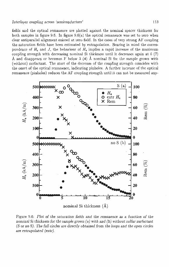
Interlayer coupling across 'semiconductors' 113
fields and the optical remanence a.re plotted against the nominal spacer thickness for both samples in figure 9.6. In figure 9.6(a) the optical remanence was set to zero when clear antiparallel alignment existed at zero field . In the cases of very strong AF coupling the saturation fields have been estimated by extrapolation. Bearing in mind the correspondence of H 5 and J, the behaviour of H. implies a rapid increase of the maximum coupling strength with decreasing nominal Si thickness until it decreases again at 6 (7) A and disappears or becomes F below 3 (4) A nominal Si for the sample grown with (without) surfactant. The start of the decrease of the coupling strength coincides with the onset of the optical remanence, indicating pinholes. A further increase of the optical remanence (pinholes) reduces the AF coupling strength until it can not be measured any-
500 00 S (a) 100 Xoo 'boo • Hs
400 x 0 0 extr Hs 80 ,........_ o~ x Rem s ,........_
300 x 60 if?. -......_ •• .__.. <i:: ...::.::: x • s .__..
~ ~
200 • >S< • 40 • x • 100 • ... 20
x • 0 0
500 no S (b) 100
400 x °<x> 80 x ,........_ ~ °too ,........_ s 300 60 if?. -......_
·~ .. .__.. <i:: s ..!<; .__.. . .. . ~ ~
200 • 40
• 100 • 20
0 0 5 10 15
nominal Si thickness (A)
Figure 9.6: Plot of the saturation ·fields and the remanence as a function of the nominal Si thickness for the sample grown (a) with and (b) without sulfur surfactant (S or no S). The full circles are directly obtained from the loops and the open circles are extrapolated (extr).
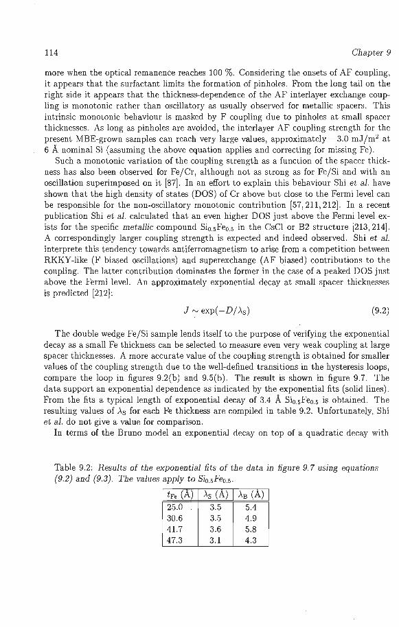
114 Chapter 9
more when the optical remanence reaches 100 %. Considering the onsets of AF coupling, it appears that the surfactant limits the formation of pinholes. From the long tail on the right side it appears that the thickness-dependence of the AF interlayer exchange coupling is monotonic rather than oscillatory as usually observed for metallic spacers. This intrinsic monotonic behaviour is masked by F coupling due to pinholes at small spacer thicknesses. As long as pinholes are avoided, the interlayer AF coupling strength for the present MBE-grown samples can reach very large values, approximately -3.0 mJ /m2 at 6 A nominal Si (assuming the above equation applies and correcting for missing Fe).
Such a monotonic variation of the coupling strength as a function of the spacer thickness has also been observed for Fe/Cr, although not as strong as for Fe/Si and with an oscillation superimposed on it [87]. In an effort to explain this behaviour Shi et al. have shown that the high density of states (DOS) of Cr above but close to the Fermi level can be responsible for the non-oscillatory monotonic contribution [57, 211, 212]. In a recent publication Shi et al. calculated that an even higher DOS just above the Fermi level exists for the specific metallic compound Si0.5Fe0.5 in the CsCl or B2 structure [213, 214]. A correspondingly larger coupling strength is expected and indeed observed. Shi et al. interprete this tendency towards antiferromagnetism to arise from a competition between RKKY-like (F biased oscillations) and superexchange (AF biased) contributions to the coupling. The latter contribution dominates the former in the case of a peaked DOS just above the Fermi level. An approximately exponential decay at small spacer thicknesses is predicted [212]:
J,...., exp(-D/ As) (9.2)
The double wedge Fe/Si sample lends itself to the purpose of verifying the exponential decay as a small Fe thickness can be selected to measure even very weak coupling at large spacer thicknesses. A more accurate value of the coupling strength is obtained for smaller values of the coupling strength due to the well-defined transitions in the hysteresis loops, compare the loop in figures 9.2(b) and 9.5(b) . The result is shown in figure 9.7. The data support an exponential dependence as indicated by the exponential fits (solid lines). From the fits a typical length of exponential decay of 3.4 A Si0.5Fe0.5 is obtained. The resulting values of As for each Fe thickness are compiled in table 9.2. Unfortunately, Shi et al. do not give a value for comparison.
In terms of the Bruno model an exponential decay on top of a quadratic decay with
Table 9.2: Results of the exponential fits of the data in figure 9. 7 using equations (9.2) and (9.3). The values apply to Si0.5Feo.5·
I ife (A) I As (A) I AB (A) I 25.0 3.5 5.4 30.6 3.5 4.9 41.7 3.6 5.8 47.3 3.1 4.3
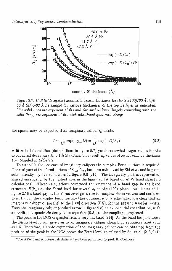
Interlayer coupling across 'semiconductors'
100
80
s 60 -<r: ~ .....__, ~r ..
::i::: 40
20
0 10 15
25.0 A Fe 30.6 A Fe
41.7 A Fe 47.3 A Fe
-- exp(-D/A.s)
- - - exp(-D/A.8 )/D2
nominal Si thickness (A)
115
Figure 9.7: Half fields against nominal Si spacer thickness for the Ge(l00)/ 80 A Fe/0-40 A Si/ 0-80 A Fe sample for various thicknesses of the top Fe layer as indicated. The solid lines are exponential fits and the dashed lines (largely coinciding with the solid lines) are exponential fits with additional quadratic decay.
the spacer may be expected if an imaginary caliper Qi exists:
1 1 J"' D 2 exp(-qi,1-D) = D 2 exp(-D/A.s) (9.3)
A fit with this relation (dashed lines in figure 9.7) yields somewhat larger values for the exponential decay length: 5.1 A Si0.5Fe0.5 . The resulting values of A.8 for each Fe thickness are compiled in table 9.2.
To establish the presence of imaginary calipers the complex Fermi surface is required. The real part of the Fermi surface of Si0.5Fe0.5 has been calculated by Shi et al. and is given, schematically, by the solid lines in figure 9.8 [214). The imaginary part is represented, also schematically, by the dashed lines in the figure and is based on ASW band structure calculations1 . These calculations confirmed the existence of a band gap in the band structure E(kl.) at the Fermi level for several k11 in the (100) plane. As illustrated in figure 2.16 a band gap at the Fermi level gives rise to complex Fermi vectors and surfaces. Even though the complex Fermi surface thus obtained is only schematic, it is clear that an imaginary caliper q; parallel to the [100] direction (rX), for the present samples, exists. From the imaginary caliper (dashed arrow in figure 9.8) an exponential contribution, with an additional quadratic decay as in equation (9.3), to the coupling is expected.
The peak in the DOS originates from a very flat band [214]. As the band lies just above the Fermi level it will give rise to an imaginary caliper along high symmetry axes such as rx. Therefore, a crude estimation of the imaginary caliper can be obtained from the position of the peak in the DOS above the Fermi level calculated by Shi et al. [213, 214]:
1The ASW band structure calculations have been performed by prof. R. Coehoorn
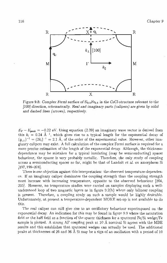
116 Chapter 9
---a---R , .... - x•qi -- .. , R
... , --- - - - - --....
qr :t_ M M
k 11
.,,,. ---- - --- ... R x R
Figure 9.8: Complex Fermi surface of Si0.5Fe0.5 in the CsCl-structure relevant to the {100} direction, schematically. Real and imaginary parts (calipers) are given by solid and dashed lines (arrows), respectively.
EF - Epeak = -0.22 eV. Using equation (2.39) an imaginary wave vector is derived from this k; = 0.24 A-1, which gives rise to a typical length for the exponential decay of (qi,J.)-1 = (2k;) - 1 = 2.1 A, of the order of the experimental value. However, other imaginary calipers may exist. A full calculation of the complex Fermi surface is required for a more precise estimation of the length of the exponential decay. Although, the thicknessdependence may be mistaken for a typical insulating (may be semiconducting) spacer behaviour, the spacer is very probably metallic. Therefore, the only study of coupling across a semiconducting spacer so far, might be that of Landolt et al. on amorphous Si [197, 199- 201].
There is one objection against this interpretation: the observed temperature-dependence. If an imaginary caliper dominates the coupling strength than the coupling strength must increase with increasing temperature, opposite to the observed behaviour [204, 205]. However, no temperature studies were carried on samples displaying such a wellunderstood loop of two magnetic layers as in figure 9.2(b) where only bilinear coupling is present. Therefore, a coupling study on such a sample would be highly desirable. Unfortunately, at present a temperature-dependent MOKE set-up is not available to do this.
The real caliper can still give rise to an oscillatory behaviour superimposed on the exponential decay. An indication for this may be found in figure 9.9 where the saturation field or the half field as a function of the spacer thickness for a sputtered Fe/ Si wedge/Fe sample is plotted. A strong AF coupling peak at 10 A nominal Si agrees with the MBE results and this establishes that sputtered wedges can actually be used. The additional peaks at thicknesses of 26 and 36 A Si may be a sign of an oscillation with a period of 10
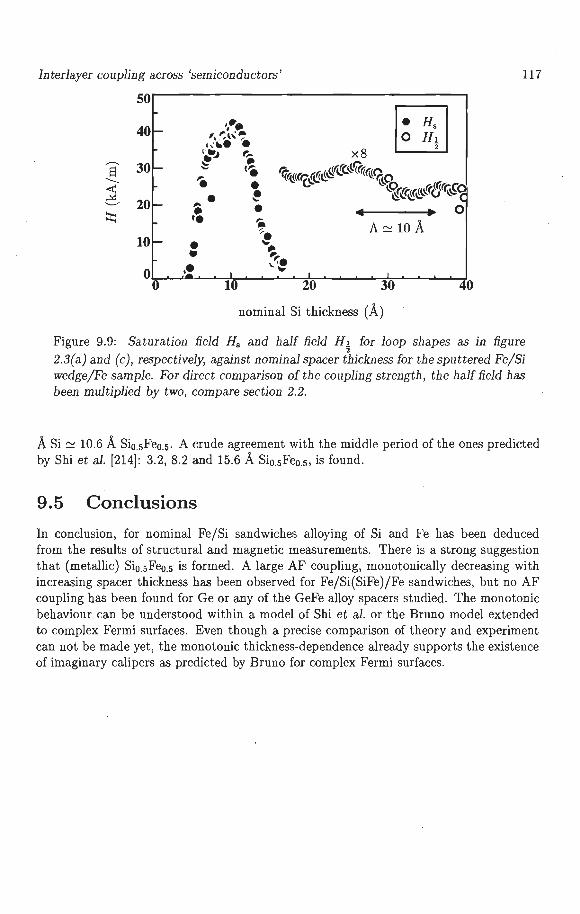
Interlayer coupling across 'semiconductors'
50
40
s 30 .......... ~ ~
20 ...__,
::r::
10
0 0
.. • •
•• 10
x8
~<{(<('(_(~l~r((efcrf((~~la ~8"~8-((~~'9
.. ,.,____ ___ ... 0
A '.:::'.10 A
20 30
nominal Si thickness (A)
117
0
Figure 9.9: Saturation field H. and half field H1 for loop shapes as in figure 2
2.3(a) and (c), respectively, against nominal spacer thickness for the sputtered Fe/Si wedge/Fe sample. For direct comparison of the coupling strength, the half field has been multiplied by two, compare section 2.2.
A Si '.::::'. 10.6 A Si0.5Fe0.5 . A crude agreement with the middle period of the ones predicted by Shi et al. [214]: 3.2, 8.2 and 15.6 A Si0.5Feo.5 , is found .
9. 5 Con cl us ions
In conclusion, for nominal Fe/Si sandwiches alloying of Si and Fe has been deduced from the results of structural and magnetic measurements. There is a strong suggestion that (metallic) Si0.5Fe0.5 is formed. A large AF coupling, monotonically decreasing with increasing spacer thickness has been observed for Fe/Si(SiFe)/Fe sandwiches, but no AF coupling has been found for Ge or any of the GeFe alloy spacers studied. The monotonic behaviour can be understood within a model of Shi et al. or the Bruno model extended to complex Fermi surfaces. Even though a precise comparison of theory and experiment can not be made yet, the monotonic thickness-dependence already supports the existence of imaginary calipers as predicted by Bruno for complex Fermi surfaces.

118 Chapter 9
Chapter 10
Summary and outlook
This thesis describes some experiments on the interlayer exchange coupling between two magnetic layers separated by a non-magnetic interlayer or spacer. As a result of this coupling the moments of the magnetic layers are inclined to align parallel or antiparallel depending on the sign of the interaction, respectively positive or negative. The former case is called ferromagnetic (F) the latter is termed antiferromagnetic (AF) coupling.
The work is part of a worldwide investigation into the phenomena in magnetic multilayers (stackings of magnetic and non-magnetic layers) which is both fundamental and application-directed and therefore receives the attention of industrial and university research groups. Interesting applications exist for e.g. magnetic anisotropy, magnetoresistance, biasing and magneto-optical effects in magnetic multilayers. Some of these properties have been studied during this PhD-work but are left outside this thesis. For the interlayer exchange coupling interesting applications exist also. However, the present study is directed somewhat more towards the fundamental side of this phenomenon.
The interest in magnetic multilayers is explained in chapter l. New properties that are expected on the basis of the layered structure and the small thickness of the layers are illustrated with examples.
Chapter 2 deals with the theory on interlayer exchange coupling, with emphasis on the Bruno model because of its tranparency and its reasonable generality. Essentially, the coupling is mediated by conduction electrons that traverse the layers, while their spin moment detects, communicates and influences the orientation of the moments of the magnetic layers. In this mediation process the wave nature of the electrons plays an important role.
The experimental techniques used to deposit magnetic multilayers and to measure the magnetic properties are the subject of chapter 3. By using wedge-shaped layers the dependence on that specific layer thickness can be studied in a single sample, which does not only save a lot of preparation time but also guarantees more constant growth conditions and a monotonically varying thickness. This motivates why this option which already existed for MBE growth, has been implemented for sputtering also. The wedge shape requires locally probing techniques for the analysis of the structure and magnetic behaviour. Such techniques are usually based on focused electron beams, like Auger electron spectroscopy and low energy electron diffraction, to characterize the growth or
119
120 Chapter 10
light beams, such as the magneto-optical Kerr effect , to measure hysteresis loops. The enormous increase of the number magnetic measurements (sometimes several thousands of loops) on a single sample with two orthogonal wedges is compensated by a speed-up of the loop measurement by two orders of magnitude.
The wave nature of the conduction electrons leads to the forming of standing waves in the electron density due to reflections on the interfaces of the spacer. If the amplitudes of these standing waves differ for spin-up and spin-down electrons, then a standing wave in the spin-density also results. The characteristic wavelength is determined by extremal spanning vectors, called calipers, of the Fermi surface of the spacer. In the case of a free electron gas the caliper equals two times the Fermi wave vector. In a measurement of the coupling strength as a function of the spacer thickness an oscillation appears with exactly this period. According to the theory the oscillation period depends on the growth orientation of the multilayer, as the length of the caliper depends on the cross section of the Fermi surface. The experiment in chapter 4 shows that the measured periods in Co/Cu/Co sandwiches in three different orientations (100), (110) and (111) agree with the predicted periods.
In the case of the (111) orientation it appeared to be difficult to prepare samples that displayed coupling, not to mention oscillation periods. Initially, this was ascribed to interface dislocations at the Co/Cu interface, due to a lattice mismatch of the bulk lattices, to which the (111) orientation is particularly sensitivity. An investigation of a Co/Au(lll)/Co sandwich with an even larger lattice mismatch, however, easily resulted interlayer coupling and even an oscillation period. Herewith these measurements indicate that in the case of Co/Cu(lll)/Co other mechanisms, as described in the literature, play the dominant role. In addition, support has been found for the predicted mechanism. The experiment has been carried out in such a way that F as well as AF coupling could be measured, see chapter 5.
The reflections mentioned are not necessarily perfect. Any transmitted electron waves through the interfaces of the spacer can reflect at the next interface and create standing waves in other layers in the same way as for the spacer. In this picture a variation of the thickness of the magnetic layers and in fact the thickness of any layer in a whole stack, should give rise to an oscillation of the coupling strength. In that case calipers of the Fermi surface of the material of the specific layer whose thickness is varied determine the periods. In chapter 6 this has been confirmed for the magnetic layers and chapter 7 for the cap layer. The experimental periods agreed with the periods thus derived. In the case of the cap layer the relation between the phases and the amplitudes of the oscillations for the various AF peaks could be quantitatively related to the theory.
Not all calipers are candidate for the oscillation periods, they are subject to certain selection rules. The in-plane component of the extremal wave vector of the Fermi surface of the spacer and any other layer must be conserved due to the in-plane translational invariance. In chapter 8 an experiment that studies the selection rules for calipers of the Cu and Ni Fermi surfaces is described. Although for Cu and Ni an exact match is not expected for the short period, a short period oscillation as a function of the Ni thickness has nevertheless been observed. Several arguments have been given that allow for small differences of the in-plane component, as is the case for Cu and Ni Fermi surfaces.
Summary and outlook 121
Apart from coupling across metallic spacers also coupling across semiconductors has been investigated using Si and Ge spacers separating two Fe layers. In. the actual samples the Si and Fe formed a SiFe alloy spacer, probably conducting metallic Si05Fe05 , as observed in the literature and the experiments in chapter 9. Similar alloying is possible for Ge but has not been checked experimentally. No AF coupling has been found for the Ge-based samples in contrast with a strong AF coupling fot the samples containing Si. Remarkably enough, the coupling strength in the Fe/Si case decreases monotonically with increasing spacer thickness. An exponential decay has been predicted on the basis of a peak in the density of states close to but above the Fermi level. In terms of the Bruno model a exponential decay (on top of a quadratic decay) is explained by tunnelling electron waves which can also mediate the coupling just like travelling electron waves. This is a consequence of the small thickness of the spacer. The position of the above-mentioned peak in the density of states allows a crude estimation of the typical length of the exponential decay: 2.1 A. Although the degree of agreement with the experimental value of 5.4 A is not yet clear, this result provides additional support for the Bruno coupling model.
The existence of spin-density waves has been confirmed by the various experiments on interlayer coupling. Implicitly this also confirms in a new way the existence of charge density waves. Already, other properties that also rely on the spin-density, have been found to depend on the spacer layer thickness in an oscillatory manner, e.g. the Kerr effect. The search for new properties with the same origin as interlayer exchange coupling will continue.
In the specific field of interlayer exchange coupling still several other points of interest remain. For example, an oscillation of the higher order biquadratic coupling strength has not been observed yet. Furthermore, the interlayer exchange coupling across insulating or semiconducting spacers deserves further investigation. Also 4d and 5d metals or metallic alloys with specific optical or electrical properties, like a negative temperature resistance coefficient or strong optical excitations, are interesting subjects for further fundamental and applied research.
122 Chapter 10
References
[l] M. Prevot, E.A. Mankinen, C.S. Gromme, and R.S. Coe, Nature 316, 230 (1985).
[2] R.S. Coe, M. Prevot, and P. Camps, Nature 374, 687 (1995).
[3] P.F. Carcia, A.D. Meinhaldt, and A. Suna, Appl. Phys. Lett . 47, 178 (1985) .
[4] W.B. Zeper, Ph.D. thesis, Technical University Twente, The Netherlands, 1991.
[5] P. Grunberg, R. Schreiber, Y. Pang, M.B. Brodsky, and H. Sowers, Phys. Rev. Lett. 57, 2442 (1986).
[6] S. Demokritov, J.A. Wolf, and P. Grunberg, Europhys. Lett. 15, 881 (1991).
[7] K. Tsutsumi and T . Fukami, J. Magn. Magn. Mater. 118, 231 (1993).
[8] M.N. Baibich, J.M. Broto, A. Fert , F. Petroff F. Nguyen Van Dau, P. Eitenne, G . Creuzet, A. Friedrich, and J .Chazelas, Phys. Rev. Lett. 61, 2472 (1988).
[9] G. Binasch, P. Grunberg, F . Saurenbach, and W. Zinn, Phys. Rev. B 39, 4828 (1989).
[10] R. Schad, C.D. Potter, P. Belien , G . Verbanck, V.V. Moshchalkov, and Y. Bruyn-seraede, Appl. Phys. Lett. 64, 3500 (1994) .
[11] P. Bruno, Phys. Rev. B 52, 411 (1995).
[12] S.S.P. Parkin, N. More, and K.P. Roche, Phys. Rev. Lett . 64, 2304 (1990).
[13] F . Nguyen van Dau, A. Fert, P. Etienne, M.N. Baibich, J .M. Broto, J. Chazelas, G. Creuzet, A. Friederich, S. Hadjoudj, H. Hurdequint, J.P. Redoules, and J. Massies, J . de Phys. 49-C8, 1633 (1988) .
[14] M. Ruderman and C. Kittel, Phys. Rev. 96, 99 (1954).
[15] T . Kasuya, Prog. Theor. Phys. :L6, 45 (1956).
[16] K. Yosida, Phys. Rev. 106, 893 (1957) .
[17] C. Kittel, in Solid State Physics, edited by F. Seitz, D. Turnbull , and H. Ehrenreich (Academic, New York and London, 1968), Vol. 22, p. 1.
123
124 References
[18] B. Dieny, J.P. Gavigan, and J.P. Rebouillat, J. Phys. Condens. Matter 2, 159 (1990) .
[19] B. Dieny and J.P. Gavigan, J. Phys. Condens. Matter 2, 178 (1990).
[20] W. Folkerts, J . Magn. Magn. Mater. 94, 302 (1991).
[21] Y. Yafet, Phys. Rev. B 36, 3948 (1987) .
[22] M.F. Crommie, C.P. Lutz, and D.M Eigler, Nature 363, 524 (1993).
[23] E.N. Economou, Green's functions in quantum physics (Springer-Verlag, Berlin, Heidelberg, New York, Tokyo, 1983) .
[24] S. Gasiorowicz, Quantum physics (Wiley, New York, Chichester, 1974).
[25] P. Bruno and C. Chappert, Phys. Rev. B 46, 261 (1992).
[26] D.J. Roaf, Phil. Trans. R. Soc. A. 255, 135 (1962).
[27] C. Chappert and J~P. Renard, Europhys. Lett . 15 , 553 (1991).
[28] D.M. Deaven, D.S. Rokhsar, and M. Johnson, Phys. Rev. B 44, 5977 (1991).
[29] R. Coehoorn, Phys. Rev. B 44, 9331 (1991) .
[30] M.D. Stiles, Phys. Rev. B 48, 7238 (1993).
[31] E.C. Snow and J.T. Waber, Phys. Rev. 157, 576 (1967).
[32] J. Callaway and C.S. Wang, Phys. Rev. B 16, 2095 (1977) .
[33] R.V. Coleman, W.H. Lowrey, and J.A. Polo, Jr. , Phys. Rev. B 23, 2491 (1981).
[34] J .L. Perez-Diaz and M.C. Munoz, Phys. Rev. B 52, 2471 (1995).
[35] N.I. Kulikov and E.T. Kulatov, J. Phys. F: Metal Phys. 12, 2267 (1982).
[36] S. Wakoh and J. Yamashita, J. Phys. Soc. Jpn. 28, 1151 (1970).
[37] C.M. Singal and T.P. Das, Phys. Rev. B 16, 5068 (1977) .
[38] F. Batallan and I. Rosenman, Phys. Rev. B 11 , 545 (1975).
[39] G.J . McMullen, D.D. Pilgram, and A. Marshall , Phys. Rev. B 46, 3789 (1992).
[40] J. Callaway and C.S. Wang, Phys. Rev. B 7, 1096 (1973).
[41] J .W.D. Connolly, Phys. Rev. 159, 415 (1967) .
[42] D.C. Tsui, Phys. Rev. 164, 669 (1967) .
[43] D.G. Laurent, J. Callaway, J.L. Fry, and N.E. Brener, Phys. Rev. B 23, 4977 (1981).

References 125
[44] O.K. Andersen and A.R. Mackintosh, Solid State Commun. 6, 285 (1968).
[45] A.P. Cracknell , The Fermi Surfaces of Metals (Taylor and Francis Ltd., London, 1971).
[46] P.J.H. Bloemen, M.T. Johnson, M.T .H. van de Vorst, R. Coehoorn, A. Reinders, J. aan de Stegge, R.M. Jungblut, and W.J.M. de Jonge, J. Magn. Magn. Mater. 148, 193 (1995) .
[47] M.T. Johnson, M.T.H. van de Vorst , P.J.H . Bloemen, R. Coehoorn, A. Reinders, J . aan de Stegge, and R. Jungblut, Phys. Rev. Lett. 75, 4686 (1995).
[48] P. Bruno, Europhys. Lett. 23 , 615 (1993) .
[49] J.B. Pendry, Low energy electron diffraction (Academic Press, London and New York, 1974).
[50] J. Barna.5, J . Magn. Magn. Mater. 111, L215 (1992).
[51] J. Barna.5, J . Magn. Magn. Mater. 128, 171 (1994).
[52] P. Bruno, J . Magn. Magn . Mater. 121, 248 (1993) .
[53] J. Mathon, Contemp. Phys. 32, 143 (1991) .
[54] D.M. Edwards and J. Mathon, J . Magn. Magn. Mater. 93, 85 (1991).
[55] J. Mathon, D.M. Edwards, R.B. Muniz, and M.S. Phan, J. Magn. Magn. Mater. 104-107, 1721 (1992).
[56] Y. Wang, P.M. Levy, and J.L. Fry, Phys. Rev. Lett. 65, 2732 (1990).
[57] Z.P. Shi, P.M. Levy, and J .L. Fry, Phys. Rev. Lett. 69, 3678 (1992) .
[58] C. Carbone, E. Vescovo, 0. Rader, W. Gudat, and W. Eberhardt, Phys. Rev. Lett. 71, 2805 (1993).
[59] J.E. Ortega, F.J. Himpsel, G.J. Mankey, and R.F. Willis, Phys. Rev. B 47, 1540 (1993).
[60] K. Garrison, Y. Chang, and P.D. Johnson, Phys. Rev. Lett. 71, 2801 (1993) .
[61] N.V. Smith, N.B. Brookes, Y. Chang, and P.D. Johnson, Phys. Rev. B 49, 332 (1994).
[62] W.R. Bennett, W. Schwarzacher, and W.F. Egelhoff, Jr., Phys. Rev. Lett . 65, 3169 (1990).
[63] Y. Suzuki and T. Katayama, in Proceedings of the Materials Research Society Conference (Materials Research Society, San Francisco, 1993), Vol. 313, p. 153.
126 References
[64] T. Katayama, Y. Suzuki, M. Hayashi , and A. Thiaville, J . Magn. Magn. Mater. 126, 527 (1993).
[65] R. Megy, A. Bounouh, Y. Suzuki, P. Beauvil!ain, P. Bruno, C. Chappert, B. Lecuyer, and P. Veillet, Phys. Rev. B 51, 5586 (1995).
[66] W. Geerts, Y. Suzuki, T. Katayama, K. Tanaka, K. Ando, and S. Yoshiha, Phys. Rev. B 50, 12581 (1994).
[67] A. Carl and D. Weller, Phys. Rev. Lett. 74, 190 (1995).
[68] Y. Suzuki and P. Bruno, J. Magn. Magn. Mater. 140-144, 651 (1995) .
[69] C.A. Dos Santos and B. Rodmacq, in Proceedings of the Materials Research Society Conference (Materials Research Society, San Francisco, 1992), Vol. 231, p. 159.
[70] M. Sakurai, N. Imamura, K. Hirano, and T . Shinjo, J. Magn. Magn. Mater. 147, 16 (1995) .
[71] z. Celinski, B. Heinrich, and J.F. Cochran, J. Appl. Phys. 70, 5870 (1991).
[72] J. Unguris, R.J. Celotta, and D.T. Pierce, J. Magn. Magn. Mater. 127, 205 (1993).
[73] R.J. Celotta, J. Unguris, and D.T. Pierce (unpublished).
[74] Z. Celinski, B. Heinrich, and J.F. Cochran (unpublished) .
[75] Q. Leng, V. Cros, R. Schiifer, A. Fuss, P. Grunberg, and W. Zinn, J. Magn. Magn. Mater. 126, 367 (1993).
[76] D.J . Keavney, D.F. Storm, J.W. Freeland, J.C. Walker, M.G. Pini , P. Politi , and A. Rettori, Phys. Rev. Lett. 71, 927 (1993).
[77] A. Fuss, S. Demokritov, P. Grunberg, and W. Zinn, J . Magn. Magn. Mater. 103, L221 (1992).
[78] K. Shintaku, Y. Daitoh, and T. Shinjo, Phys. Rev. B 47, 14584 (1993).
[79] J. Unguris, R.J. Celotta, and D.T. Pierce, J. Appl. Phys. 75, 6437 (1994).
[80] K. Takanashi, R. Schreiber, I. Mertig, and P. Grunberg, J. Magn. Magn. Mater. 156, 237 (1996).
[81] M. Pomerantz, J .C. Slonczewski., and E. Spiller, J . Appl. Phys. 61 , 3747 (1987).
[82] S.T. Purcell, W. Folkerts, M.T. Johnson, N.W.E. McGee, K. Jager, J . aan de Stegge, W.B. Zeper, W. Hoving, and P. Grunberg, Phys. Rev. Lett. 67, 903 (1991) .
[83] J. Unguris, R.J. Celotta, and D.T. Pierce, Phys. Rev. Lett. 67, 140 (1991).
References 127
[84] E.E. FUilerton, M.J. Conover, J.E. Mattson, C.H. Sowers, and S.D. Bader, Phys. Rev. B 48, 15755 (1993).
[85] S.O. Demokritov, J.A. Wolf, and P. Grunberg, J. Magn. Magn. Mater. 126, 386 (1993).
[86] B. Heinrich, M. From, J.F. Cochran, L.X. Liao, Z. Celinski, C.M. Schneider, and K. Myrtle, in Proceedings of the Materials Research Society Conference (Materials Research Society, San Francisco, 1993), Vol. 313, p. 119.
[87] J .A. Wolf, Q. Leng, R. Schreiber, P. Grunberg, and W. Zinn, J. Magn. Magn. Mater. 121, 253 (1993).
[88] W. Folkerts and F. Hakkens, J . Appl. Phys. 73, 3922 (1993).
[89] K. Takanashi, H. FUjimori, Y. Obi, and N. Tsuda, J. Magn. Magn. Mater. 121, 309 (1993) .
[90] M.T. Johnson, S.T. Purcell, N.W.E. McGee, R. Coehoorn, J. aan de Stegge, and W. Hoving, Phys. Rev. Lett. 68, 2688 (1992).
[91] B. Heinrich, Z. Celinski, J.F. Cochran, A.S. Arrott, K. Myrtle, and S.T. Purcell, Phys. Rev. B 47, 5077 (1993) .
[92] Z. Celinski and B. Heinrich, J . Magn. Magn. Mater. 99, L25 (1991) .
[93] F . Petroff, A. Bartelemy, D.H. Mosca, D.K. Lottis, A. Fert, P.A. Schroeder, W.P. Pratt, Jr., R. Laloee, and S. Lequin, Phys. Rev. B 44, 5355 (1991).
[94] S.T. Purcell, M~T. Johnson, N.W.E. McGee, R. Coehoorn, and W. Hoving, Phys. Rev. B 45, 13064 (1992).
[95] T.G. Walker and H. Hopster, in Proceedings of the Materials Research Society Conference (Materials Research Society, San Francisco, 1993), Vol. 313, p. 381.
[96] Z.Q. Qiu, J. Pearson, A. Berger, and S.D. Bader, Phys. Rev. Lett. 68, 1398 (1992).
[97] M.E. Brubaker, J .E. Mattson, C.H. Sowers, and S.D. Bader, Appl. Phys. Lett. 58, 2306 (1991 ).
[98] J.E. Mattson, C.H. Sowers, A. Berger, and S.D. Bader, Phys. Rev. Lett. 68, 3252 (1992).
[99] Z. Celinski, B. Heinrich, W.B. Muir, A.S. Arrott, and J. Kirschner, Phys. Rev. Lett. 65, 1156 (1990) .
[100] K. Totland, P. FUchs, J.C. Grobli, and M. Landolt, Phys. Rev. Lett. 70, 2487 (1993) .
[101] J .E. Mattson, S. Kumar, E.E. FUilerton, S.R. Lee, C.H. Sowers, M. Grimsditch, S.D. Bader, and F.T . Parker, Phys. Rev. Lett. 71, 185 (1993).
128 References
[102] J.E. Mattson, E.E. Fullerton, S. Kumar, S.R. Lee, C.H. Sowers, M. Grimsditch, S.D. Bader, and F.T. Parker, J. Appl. Phys. 75, 6169 (1994).
[103] Q.Y. Jin, M. Lu, Q.S. Bie, Y.B. Xu, H.R. Zhai, and Y.H. Shen, J. Magn. Magn. Mater. 140-144, 565 (1995).
[104] L. Wu and T. Shinjo, J. Magn. Magn. Mater. 125, L14 (1993).
[105] J.J. de Vries, W.J.M. de Jonge, M.T. Johnson, J. aan de Stegge, and A. Reinders, J. Appl. Phys. 75, 6440 (1994).
[106] J.J. de Vries, P.J.H. Bloemen, M.T. Johnson, J. aan de Stegge, A. Reinders, and W.J.M. de Jonge, J. Magn. Magn. Mater. 129, L129 (1994).
[107] V. Colier, D. Renard, B. Bartenlian, P. Beau villain, C. Chappert, C. Dupas, J. Ferre, M. Galtier, E. Kolb, M. Mulloy, J.P. Renard, and P. Veillet, Phys. Rev. Lett. 71, 3023 (1993).
[108] T. Takahata, S. Araki, and T. Shinjo, J. Magn. Magn. Mater. 82, 287 (1989).
[109] N. Metoki, W. Donner, Th. Zeidler, and H. Zabel, J. Magn. Magn. Mater. 126, 397 (1993).
[llCI] S.S.P. Parkin, Phys. Rev. Lett. 67, 3598 (1991).
[111] P.J.H. Bloemen, W.J.M. de Jonge, and H.C. Donkersloot, J. Appl. Phys. 73, 4522 (1993).
[112] Z.Q. Qiu, J. Pearson, and S.D. Bader, Phys. Rev. B 46, 8659 (1992).
[113] J.J. de Miguel, A. Cebollada, J.M. Gallego, R. Miranda, C.M. Schneider, P. Schuster, and J. Kirschner, J. Magn. Magn. Mater. 93, 1 (1991).
[114] P.J.H. Bloemen, M.T. Johnson, M.T.H. van de Vorst, R. Coehoorn, J.J. de Vries, R. Jungblut, J. aan de Stegge, A. Reinders, and W.J.M. de Jonge, Phys. Rev. Lett. 72, 764 (1994).
[115] M.T. Johnson, R. Coehoorn, J.J. de Vries, N.W.E. McGee, J. aan de Stegge, and P.J.H. Bloemen, Phys. Rev. Lett. 69, 969 (1992).
[116] S.N. Okuno and K. Inomata, Phys. Rev. Lett. 70, 1711 (1993).
[117] P.J.H. Bloemen, M.T. Johnson, J. aan de Stegge, and W.J.M. de Jonge, J. Magn. Magn. Mater. 116, L315 (1992).
[118] S.S.P. Parkin, R.F. Marks, R.F.C. Farrow, C.R. Harp, Q.H. Lam, and R.J. Savoy, Phys. Rev. B 46, 9262 (1992).
[119) J. Kohlhepp, S. Cordes, H.J. Eimers, and U. Gradmann, J. Magn. Magn. Mater. 111, L231 (1992).
References 129
[120] U. Gradmann, H.J. Elmers, and J . Kohlhepp, in Proceedings of the Materials Research Society Conference (Materials Research Society, San Francisco, 1993), Vol. 313, p. 107.
[121] A. Schreyer, K. Bro!, J.F. Ankner, Th. Zeidler, P. Bodeker, N. Metoki, C.F. Majkrzak, and H. Zabel, Phys. Rev. B 47, 15334 (1993) .
[122] M.A. Howson, B.J. Hickey, J. Xu, D. Grieg, and N. Wiser, Phys. Rev. B 48, 1322 (1993).
[123] D.H. Mosca, F. Petroff, A. Fert, P.A. Schroeder, W.P. Pratt, Jr., and R. Laloee, J. Magn. Magn. Mater. 94, Ll (1991).
[124] S.S.P. Parkin, R. Bhadra, and K.P. Roche, Phys. Rev. Lett. 66, 2152 (1991).
[125] W.F. Egelhoff, Jr. and M.T. Kief, Phys. Rev. B 45, 7795 (1992) .
[126] D. Greig, M.J. Hall, M.A. Howson, B.J. Hickey, M.J. Walker, and J. Xu, in Proceedings of the Materials Research Society Conference (Materials Research Society, San Francisco, 1993), Vol. 313, p. 3.
[127] S.S.P. Parkin, C. Chappert, and F . Herman, Europhys. Lett. 24, 71 (1993).
[128] J.F. Bobo, L. Hennet, and M. Piecuch, J. Magn. Magn. Mater. 140-144, 587 (1995).
[129] J.F. Bobo, L. Hennet, and M. Piecuch, Europhys. Lett. 24, 139 (1993).
[130] S.S.P. Parkin, C. Chappert, and F. Herman, in Proceedings of the Materials Research Society Conference (Materials Research Society, San Francisco, 1993), Vol. 313, p. 179.
[131] P.J.H. Bloemen, R. Coehoorn, and W.J.M. de Jonge, J. Magn. Magn. Mater. 121, 306 (1993).
[132] P.J.H. Bloemen, R. van Dalen, W.J.M. de Jonge M.T. Johnson, and J. aan de Stegge, J. Appl. Phys. 73, 5972 (1993).
[133] J.C. Bruyere, 0. Massenet, R. Montmory, and L. Neel, IEEE Trans. Magn. 0, 0 (1965).
[134] P.J.H. Bloemen, E.A.M. van Alphen, and W.J.M. de Jonge, J. Magn. Magn. Mater. 104-107, 1775 (1992).
[135] P.P. Freitas, L.V. Melo, I. Trindade, and M. From, J. Magn. Magn. Mater. 116, 92 (1992).
[136] P.P. Freitas, L.V. Melo, I. Trindade, M. From, J. Ferreira, and P. Monteiro, Phys. Rev. B 45, 2495 (1992).
130 References
[137] P.J .H. Bloemen, H.W. van Kesteren, H.J .M. Swagten, and W.J.M. de Jonge, Phys. Rev. B 50, 13505 (1994).
[138] S.S.P. Parkin and D. Mauri, Phys. Rev. B 44, 7131 (1991).
[139] J. Fassbender, F. Nortemann, R.L. Stamps, R.E. Carnley, B. Hillebrands, and G. Gi.intherodt, Phys. Rev. B 46, 5810 (1992).
[140] K. Ounadjela, D. Muller, A. Dinia, A. Arbaoui, P. Panissod, and G. Suran, Phys. Rev. B 45, 7768 (1992).
[141] K. Ounadjela, A. Arbaoui, A. Herr, R. Poinsot , A. Dinia, D. Muller, and P. Pan-issod , J. Magn. Magn. Mater. 104-107, 1896 (1992).
[142] Z. Zhang, L. Zhou, P.E. Wigen, and K. Ounadjela, J . Appl. Phys. 75, 6434 (1994) .
[143] A. Arbaoui , A. Dinia, and P. Panissod, Solid State Commun. 85, 475 (1993).
[144] A. Murayama, M. Miyamura, K. Nishiyama, K. Miyata, and Y. Oka, J. Appl. Phys. 69, 5661 (1991) .
[145] Z. Zhang, P.E. Wigen, and S.S.P. Parkin, J. Appl. Phys. 69, 5649 (1991).
[146] P.J.H. Bloemen, M.T.H. van der Vorst, M.T. Johnson, R. Coehoorn, and W.J.M. de Jonge, J. Appl. Phys. 76, 7081 (1994).
[147] P.J.H. Bloemen, M.T.H. van der Vorst, W.J .M. de Jonge, M.T. Johnson, and R. Coehoorn, Modern Physics Letters B 9, 1 (1995) .
[148] S.N. Okuno and K. Inomata, Phys. Rev. Lett. 72, 1553 (1994) .
[149] S.N. Okuno and K. Inoumata, Phys. Rev. B 51, 6139 (1995) .
[150] J .J . de Vries, M.T. van de Vorst, M.T. Johnson, A. Reinders, and W.J.M. de Jonge, Phys. Rev. B 54, 748 (1996).
[151] J .J . de Vries, A.A.P. Schudelaro, R. Jungblut, A. Reinders, J. Kohlhepp, R. Coehoorn, and W.J.M. de Jonge, Phys. Rev. Lett . 75, 4306 (1995).
[152] J.J. de Vries, A.A.P. Schudelaro, R.M. Jungblut, and W.J .M. de Jonge, J. Magn. Magn. Mater. 156, 257 (1996).
[153] S.N. Okuno and K. Inomata, J. Phys. Soc. Jpn. 64, 3631 (1995).
[154] A. Bounouh, P. Beauvillain, P. Bruno, C.Chappert, R. Megy, and P. Veillet, Europhys. Lett. 33, 315 (1996).
[155] G.W. Anderson, M.C. Hanf, P.R. Norton, Z.H. Lu, and M.J. Graham, Appl. Phys. Lett . 66 , 1123 (1995).
[156] G.R. Harp and S.S.P.Parkin, Appl. Phys. Lett. 65, 3063 (1994) .

References
[157] G.R. Harp and S.S.P.Parkin (unpublished).
[158] X. Bian, H.T. Hardner, and S.S.P. Parkin, J. Appl. Phys. 79, 4980 (1996).
[159] J. Kerr, Phil. Mag. 3, 339 (1877).
[160] M. Mansuripur, J. Appl. Phys. 67, 6466 (1990).
[161] R.P. Hunt, J. Appl. Phys. 38, 1652 (1967).
[162] K. Sato, Jpn. J. Appl. Phys. 20, 2403 (1981).
[163] P. Bruno and C. Chappert, Phys. Rev. Lett. 67, 1602 (1991).
131
[164] R. Coehoorn, M.T. Johnson, W. Folkerts, S.T. Purcell, N.W.E. McGee, A. de Veirman, and P.J.H. Bloemen, Magnetism and Structure in Systems of reduced Dimension (Plenum Press, New York, 1993), proceedings of the NATO Advanced Research Workshop on Corsica, June 15-19, 1992.
[165] J. Kohlhepp (unpublished).
[166] L. Nordstrom, P. Lang, R. Zeller, and P.H. Dederichs, Phys. Rev. B 50, 13058 (1994).
[167] Metals Handbook, Metallography, Structures and Phase Diagrams, 8 ed. (American Society for Metals, 1973), Vol. 8.
[168] in Solid State Physics: Magnetic properties of metals, edited by Landolt-Bornstein (Springer Verlag, Berlin, 1996), Vol. III/19b, Chap. 1.5.1.6, p. 62, fig. 127.
[169] S.A. Ahern, M.C.J. Martin, and W. Sucksmith, Proc. R. Soc. London A248, 145 (1958).
[170] R. Miranda, Physica Scripta T49, 579 (1993).
[171] P.J.H. Bloemen and W.J.M. de Jonge, J. Magn. Magn. Mater. 116, Ll (1992).
[172] J. de la Figuera, J.E. Prieto, C. Ocal, and R. Miranda, Phys. Rev. B 47, 13043 (1993).
[173] J.J. de Vries (unpublished).
[174] P. Beauvillain, P. Bruno, J.P. Chauyinaeu, M. Galtier, K. Le Dang, C. Marliere, R. Megy, D. Renard, J. Seiden, F. Trigui, P. Veillet, and E. Velu, J. Magn. Magn. Mater. 94, 319 (1991).
[175] C. Chappert, K. Le Dang, P. Beauvillain, H. Hurdequint, and D. Renard, Phys. Rev. B 34, 3192 (1986).
[176] F.J.A. den Broeder, W. Hoving, and P.J.H. Bloemen, J. Magn. Magn. Mater. 93, 562 (1991).
132 References
[177] P.J.H. Bloemen, W.J.M. de Jonge, and F.J.A. den Broeder, J. Magn . Magn. Mater. 93, 105 (1991).
[178] V. Zlatic, Solid State Commun. 86, 523 (1993).
[179] S.S.P. Parkin, R.F.C. Farrow, R.F. Marks, A. Cebollada, G.R. Harp, and R.J. Savoy, Phys. Rev. Lett. 72, 3718 (1994).
[180] U. Gradmann and H.J. Elmers, J. Magn. Magn. Mater. 137, 44 (1994).
[181] E.A.M. van Alphen, S.G.E. te Veldhuis, H.A.M. de Gronckel, K. Kopinga, and W.J .M. de Jonge, Phys. Rev. B 49, 17336 (1994).
[182] E.A.M. van Alphen and W.J.M. de Jonge, Phys. Rev. B 51, 8182 (1995).
[183] P. Bruno and C. Chappert, Phys. Rev. Lett. 67, 2592 (1991).
[184] R. Coehoorn and J.P.W.B. Duchateau , J . Magn. Magn. Mater. 126, 390 (1993).
[185] A. Fert and P. Bruno, in Ultrathin Magnetic Structures, edited by B. Heinrich and J.A.C. Bland (Springer Verlag, Berlin, Heidelberg, 1994), Vol. II , Chap. 2.2, p. 82.
[186] K.B. Hathaway, in Ultrathin Magnetic Structures, edited by B. Heinrich and J .A.C. Bland (Springer Verlag, Berlin, Heidelberg, 1994), Vol. II, Chap. 2.1, p. 45.
[187] private communication P. Bruno.
[188] G. Xiao and C.L. Chien, J. Appl. Phys. 61, 4061 (1987).
[189] M.A.M. Gijs, S.K.J. Lenczowski, and J .B. Giesbers, Phys. Rev. Lett. 70, 3343 (1993) .
[190] M.A.M. Gijs, S.K.J. Lenczowski, and J.B . Giesbers, in Proceedings of the Materials Research Society Conference (Materials Research Society, San Francisco, 1993), Vol. 313, p. 11.
[191] M.A.M. Gijs, J.B. Giesbers, S.K.J. Lenczowski, and H.H.J.M. Janssen, Appl. Phys. Lett. 63, 111 (1993).
[192] P.A. Schroeder, J. Bass, P. Holody, S.F. Lee , R. Loloee, W.P. Pratt, Jr., and Q. Yang, in Proceedings of the Materials Research Society Conference (Materials Research Society, San Francisco, 1993), Vol. 313, p. 47.
[193] W.P. Pratt, Jr., S.F. Lee, J.M. Slaughter, R. Loloee, P.A. Schroeder, and J. Bass, Phys. Rev. Lett. 66, 3060 (1991).
[194] S.F. Lee, W.P. Pratt, Jr., R. Loloee, P.A. Schroeder, and J . Bass, Phys. Rev. B 46, 548 (1992) .
[195] L.J . Maksymowicz, A.Z. Maksymowicz, and H. Jankowski, J . Magn. Magn. Mater. 73, 11 (1988) .
References 133
[196] Y. Liu, X. Ma, and L. Mei, J. Phys. Condens. Matter 3, 3571 (1991) .
[197] S. Toscano, B. Briner, H. Hopster, and M. Landolt, J. Magn. Magn. Mater. 114, L6 (1992).
[198] E.E. Fullerton, J.E. Mattson, S.R. Lee, C.H. Sowers Y.Y. Huang, G. Fletcher, S.D. Bader, and F .T.Parker, J. Magn. Magn. Mater. 117, L301 (1992).
[199] B. Briner and M. Landolt, Z. Phys. B 92, 1 (1993) .
[200] B. Briner and M. Landolt, Phys. Rev. Lett. 73, 340 (1994) .
[201] B. Briner and M. Landolt, Europhys. Lett. 28, 65 (1994).
[202] K. Inomata, K. Yusu, and Y. Saito, Phys. Rev. Lett. 74, 1863 (1995).
[203] K. Inomata, K. Yusu, and Y. Saito, Jpn. J. Appl. Phys. 33, Ll670 (1994).
[204] F.J.A. den Broeder and J. Kohlhepp, Phys. Rev. Lett . 75, 3026 (1995).
[205] J. Kohlhepp and F .J .A. den Broeder, J . Magn. Magn. Mater. 156, 261 (1996).
[206] A. Chaiken, R.P. Michel, and M.A. Wall, Phys. Rev. B 53, 5518 (1996) .
[207] B. Briner, Ph.D. thesis, Swiss federal institute of technology, Zurich, Switzerland, 1994.
[208] in Solid State Physics: Magnetic properties of metals, edited by Landolt-Bornstein (Springer Verlag, Berlin, 1996), Vol. III/19, Chap. il, p. 41, fig. 10.
[209] E.E. Fullerton and S.D. Bader, Phys. Rev. B 53, 5112 (1996).
[210] J. Kohlhepp, M. Valkier, A. van der Graaf, and F.J .A. den Broeder (to be published in Phys. Rev. B) .
[211] Z.P. Shi, P.M. Levy, and J.L. Fry, Phys. Rev. B 49, 15159 (1994).
[212] Z.P. Shi, P.M. Levy, and J.L. Fry, Europhys. Lett. 26, 473 (1994).
[213] Z.P. Shi and B.M. Klein (unpublished).
[214] Z.P. Shi, B.M. Klein, and Z.W. Lu (unpublished).
134 References
List of publications
Chapter 4
Orientational dependence of the oscillatory exchange interaction in Co/Cu/Co M.T. Johnson, R. Coehoorn, J.J. de Vries, N.W.E. McGee, J. aan de Stegge, and P.J.H. Bloem en Phys. Rev. Lett. 69, 969 (1992).
Orientational dependence of the oscillatory exchange coupling M.T. Johnson, P.J .H. Bloemen, R. Coehoorn, J.J. de Vries, N.W.E. McGee, R. Jungblut, A. Reinders, and J . aan de Stegge Proceedings of the Materials Research Society Conference (Materials Research Society, San Francisco, 1993), Vol. 313, p. 93.
Chapter 5
Oscillatory interlayer exchange coupling in Co/ Au(lll)/ Co J.J. de Vries, P.J .H. Bloemen, M.T. Johnson, J . aan de Stegge, A. Reinders, and W.J.M. de Jonge J . Magn. Magn. Mater. 129, L129 (1994).
Oscillation of the interlayer coupling in Co/ Au(lll)Co J.J. de Vries, W.J.M. de Jonge, M.T. Johnson, J. aan de Stegge, and A. Reinders J . Appl. Phys. 75, 6440 (1994).
Chapter 6
Magnetic layer thickness dependence of the interlayer exchange coupling in (001) Co/Cu/Co P.J.H. Bloemen, M.T. Johnson, M.T .H. van de Vorst, R. Coehoorn, J .J. de Vries, R. Jungblut, J. aan de Stegge, A. Reinders, and W.J.M. de Jonge Phys. Rev. Lett. 72, 764 (1994).
Chapter 7
Oscillatory interlayer exchange coupling with the Cu cap layer thickness in Co/Cu/Co/ -
135
136 List of publications
Cu(lOO) J.J. de Vries, A.A.P. Schudelaro, R. Jungblut , A. Reinders , J . Kohlhepp, R. Coehoorn, and W.J.M. de Jonge Phys. Rev. Lett. 75, 4306 (1995) .
Oscillatory behaviour of the interlayer coupling with the thickness of the Cu cap layer in Co/Cu(lOO) J.J. de Vries and A.A.P. Schudelaro and R. Jungblut, and W.J.M. de Jonge J. Magn. Magn. Mater. 156, 257 (1996)
Chapter 8
Biperiodic oscillatory coupling as a function of the thickness of an embedded Ni layer in Co/Cu/Co/Ni/Co(lOO) and selection rules for the periods J.J. de Vries, M.T. van de Vorst, R. Jungblut, M.T . Johnson, A. Reinders, P.J.H. Bloemen, R. Coehoorn, and W.J.M. de Jonge Phys. Rev. B 54, 748 (1996)
Chapter 9
Structural and magnetic analysis of MEE-grown Fe/Si/Fe and Fe/ Ge/Fe sandwiches J .J . de Vries, J. Kohlhepp, F.J.A. den Broeder, P.A. Verhaegh, R, Jungblut, A. Reinders, and W.J .M. de Jonge J. Magn. Magn. Mater. (to be published)
Not contained in this thesis
Orientational dependence of the interface magnetic anisotropy in epitaxial Ni/Co/Ni sandwiches M.T. Johnson, J.J. de Vries, N.W.E. McGee, J. aan de Stegge, and F.J.A. den Broeder Phys. Rev. Lett. 69, 3575 (1992).
Perpendicular anisotropy of epitaxial 'wedge-shaped' Co/Ni sandwiches grown on single crystal Cu substrates M.T. Johnson, F.J.A. den Broeder, J.J . de Vries, N.W.E. McGee, R. Jungblut, and J. aan de Stegge J. Magn. Magn. Mater. 121, 494 (1993) .
Localized Kerr study of the magnetic properties of an ultrathin epitaxial Co wedge grown on Pt(lll) · N.W.E. McGee, M.T. Johnson, J.J . de Vries , and J. aan de Stegge J . Appl. Phys. 73, 3418 (1993) .
List of publications 137
Local structural and polar Kerr effect measurements on an ultrathin epitaxial Co wedge grown on Pd(lll) S.T. Purcell, M.T. Johnson, N.W.E. McGee, J .J . de Vries, W.B. Zeper, and W. Hoving J. Appl. Phys. 73, 1360 (1993).
Loose spins in Co/Cu(lOO) J .J . de Vries, G.J. Strijkers, M.T. Johnson, A. Reinders , and W.J .M. de Jonge J. Magn . Magn. Mater. 148, 187 (1995).
Correlation between the spin magnetic dipole term and the magnetic anisotropy in Co/Pd multilayers C.F.J . Flipse, J .J . de Vries, G . van der Laan, M. Surman, A. Partridge, and W.J.M. de Jonge J. Magn. Magn. Mater. 148, 141 (1995) .
Magnetic anisotropy in multilayers M.T. Johnson, P.J .H. Bloemen, F.J.A. den Broeder, and J.J . de Vries Rep. Prog. Phys. 59, 1 (1996) .
138 List of publications
Samenvatting
Dit proefschrift beschrijft enkele experimenten a.an de tussenlaag-uitwisselingskoppeling tussen twee magnetische lagen die gescheiden zijn door een niet-magnetische tussenlaag. Als gevolg van deze koppeling hebben de momenten van de magnetische lagen de neiging parallel of antiparallel te gaan staan al naar gelang het teken van de koppeling, respectivelijk plus en min. Het eerste geval heet ferromagnetische (F) koppeling het tweede antiferromagnetische (AF) koppeling.
Het werk maakt deel uit van een wereldwijd onderzoek naar de verschijnselen in magnetische multilagen (een stapeling magnetische en niet-magnetische lagen) <lat zowel fundamenteel als toepassingsg;ericht is en daarom de aandacht heeft van industriele en universitaire onderzoeksgroepen. Voor bijvoorbeeld magnetische anisotropie, magnetoweerstand, biasing en magneto-optische effecten in magnetische multilagen bestaan interessante toepassingen. Enkele van deze eigenschappen zijn ook tijdens de promotie bestudeerd maar buiten het bestek van <lit proefschrift gebleven. Ook voor de tussenlaagkoppeling bestaan interessante toepassingen. Het onderzoek hier is echter meer gericht op de fundamentele kant van <lit verschijnsel.
De belangstelling voor magnetische multilagen wordt gemotiveerd in hoofdstuk 1. Nieuwe eigenschappen, die te verwachten zijn op grond van de gelaagde structuur en de geringe dikte van de lagen, warden geillustreerd met voorbeelden.
Hoofdstuk 2 beschrijft de theorie voor tussenlaag-uitwisselingskoppeling. De nadruk ligt daarbij op het model van Bruno vanwege de inzichtelijkheid en de redelijke algemeenheid. In essentie komt de koppeling tot stand doordat geleidingselectronen door de lagen heen bewegen, terwijl hun spinmoment de orientatie van de momenten van de magnetische lagen registreert, overdraagt en belnvloedt. Bij de overdracht van de koppeling speelt het golfkarakter van de electronen een belangrijke rol.
De gebruikte technieken om magnetische multilagen te maken en de magnetische eigenschappen daarvan te meten zijn het onderwerp van hoofdstuk 3. Door wigvormige lagen te gebruiken kan de dikteafhankelijkheid bestudeerd warden in een enkel preparaat hetgeen niet alleen preparatietijd bespaart maar ook constantere groei-omstandigheden en een monotoon dikteverloop garandeert . Dit verklaart waarom deze mogelijkheid, die voor opdampen al bestond, ook voor sputterdepositie is ingevoerd. De wigvorm brengt met zich mee <lat de analysetechnieken .voor de structuur en de magnetische karakterisatie locaal moeten kunnen meten. Dergelijke technieken zijn vaak gebaseerd op gefocusseerde electronenbundels, bijvoorbeeld Auger electronen spectroscopie en lage energie electronen diffractie voor karakterisatie van de groei, of lichtbundels, zoals bij het magneto-optische Kerr effect voor het meten van hystereselussen. De enorme toename van het aantal
139

140 Samenvatting
magnetische metingen (soms enkele duizenden) aan een preparaat met twee onderling loodrechte wiggen, wordt gecompenseerd door een gerealiseerde versneiling van de Kerr meettechniek met twee ordegroottes.
Het golfkarakter van geleidingselectronen leidt ertoe dat staande gdlven ih de electronendichtheid gevormd worden door refiecties aan de grensvlakken van de tussenlaag. Als de amplitudes van deze staande golven verschillen voor spin-op en spirH1eer electrdnen zal er ook een staande golf in de spindichtheid ontstaan . De karaktefistieke golfiengte wordt bepaald door extremale overspanningsvectoren van het Ferml-dppervlak Voor een vrij-electrongas is dat de Fermi·golfvectot, Bij meting van de koppeliilgssterkte als functie van de tussenlaagdikte ontstaat een oscillatie rriet preties deze periode. Volgens deze theorie hangt de periode af van de groeiorlentatie van de multilaag. De extremale overspanningsvectoren hangen namelijk af van de doorsnijdingsrichtirig van het Fermioppervlak. Het experiment in hoofdstuk 4 laat zien dat de gemeten perioden in Co/Cu/Co preparaten in drie verschillende orientaties (100), (110) en (111) overeenstemmen met de aldus verwachte perioden.
Voor de (111)-orientatie bleek het moellijk om prepapraten te groeien die koppeling vertoonden, faat staan oscillatieperioden. bit werd aanvankelijk toegeschreven aan groeifouten aan het Co/Cu grensvlak, ten gevolge van mispassing tussen de bulk roosterparameters, waarvoor met name de (111 )-orientatie gevoelig zou zijn. Een experiment aan Co/Au(Ill) met een nog veel grotere mispassing gaf echter niet veel problernen Om zelfs de oscillatieperiode te bepalen. Het experiment toonde daarmee aan d·at voor Co/Cu(lll) andere mechanismen , zoals in de literatuur vermeld, hoofdverantwoordelijk zijn. Tegelijkertijd ondersteunen de metingen aan Co/ Au(lll) het bestaan van het bovenstaande mechanisme. Het experiment is zo uitgevoerd dat zowel F als AF koppeling gemeten kon worden. Dit is beschreven in hoofdstuk 5.
De genoemde refiecties aan de grensvlakken van de tussenlaag hoeven niet volledig te zijn. Eventuele doorgaande electronengolven kunnen, net zo goed als d;at in de tussenlaag het geval was, refiecteren aan volgende grensvlakken en staande golverl opwekken. Volgens dit beeld zou er als functie van de magnetische laagdikte, en eigenlijk als functie van elke laaggdikte, ook een oscillatie van de koppelingssterkte moeten optreden. In dit geval levert het Fermi oppervlak van de magnetische laag de pefiode. In hoofdstuk 6 wordt dit experimenteel bevestigd voor de magnetische laag en in hoofdstuk 7 voor de afdeklaag. Deze waarnemingen zijn in overeenstemming met en ondersteunen de theoretische modellen.
Niet zomaar alle extremale overspanningsvectoren van het Fermi ' oppervlak van de magnetische laag komen in aanmerkfog voor oscillatieperioden. Ze moeten wel de in~vlak component van de extremale golfvectoren van bet Fermi-oppervlak van de tusserilaag behouden; vanwege de in-vlak translatiesymmetrie. Voor de Fermi-oppervlakken van Cu en Ni wordt verwacht dat de in-vlak golfvectoren van de korte periode bijna maar niet precies gelijk zijn, terwijl een oscillatie met een korte periode als functie van de Ni laagdikte we! is waargenomen in het experiment vari hoofdstuk 8. Dit laat zien dat een : klein verschil in de in-vlak component toegestaan is. Enkele argumenten hiervoor worden gegeven.
Behalve onderzoek naar de koppeling ' tussen magnetische lagen over niet-magnetische metalen tussenlagen is er ook orrderzoek gedaan· naar de koppeling over halfgeleidende
Samenvatting 141
tussenlagen zoals Si en Ge tussen twee Fe lagen. Uit de experimenten in hoofdstuk 9 evenals uit die in de literatu ur blijkt echter <lat de Si tussenlaag met de (bovenste) Fe laag reageert tot een SiFe-legering, vermoedelijk geleidend, metallisch Si0.5Fe0.5 in de CsClstructuur. Een analoge GeFe vorming is mogelijk maar niet door experimenten gecontroleerd. Wat betreft de koppeling over Ge en enkele GeFe-legeringen is geen AF koppeling vastgesteld, terwijl een sterke AF koppeling over Si0.5Fe0.5 (vermoedelijk) tussenlagen is gemeten. Bijzonder is <lat de koppelingsterkte in <lit Iaatste gevaJ monotoon daalt met de tussenlaagdikte. Op basis van een hoge toestandsdichtheid vlak boven het Fermi niveau is een exponentieel verloop voorspeld. In termen van het Bruno model kan een exponentieel verloop bovenop een kwadratische verloop verklaard worden doordat naast oscillerende electrongolven ook tunnelende electrongolven tot koppeling leiden, ook voor metalen. Dit is het gevolg van de geringe dikte van de tussenlaag. Op grond van de positie van bovengenoemde hoge toestandsdichtheid mag ruwweg een lengte voor de exponentiele afval van 2.1 A verwacht worden. Deze waarde is van de zelfde ordeals een typische lengte van 5.4 A in het experiment. Hoewel de mate van overeenstemming nog niet helemaal duidelijk is, is ook dit resultaat een belangrijke ondersteuning van het Bruno model.
142 Sam en vatting
Dankwoord
Tot slot wil ik graag iedereen bedanken die heeft bijgedragen aan de totstandkoming van <lit proefschrift en deze promotie tot een zo boeiende periode heeft gemaakt. Een aantal personen wil ik met name bedanken:
• Wim de Jonge voor zijn inspirerende begeleiding en de kritische opmerkingen tijdens de vele discussies over resultaten en ideeen.
• Prof. J .A. Pals voor het nauwkeurig doorlezen van het proefschrift en de belangstelling tijdens de promotie.
• Pascal Bloemen voor zijn actieve betrokkenheid bij het werk en zijn aanstekelijke enthousiasme.
• Reinder Coehoorn voor het uitvoeren van ASW berekeningen.
• Jelto Smits en Frans Greidanus voor de geboden samenwerking met de groep Magnetisme van Philips Research.
• Mark Johnson, Reiner Jungblut, Frits den Broeder, Jos aan de Stegge, Bart Reinders, Jiirgen Kohlhepp, Reinder Coehoorn, Nigel McGee en Erik Janssen (het Memula-team) voor de wetenschappelijke discussies en ondersteuning en de gezelligheid.
• De studenten Igor Bogaert, Eric Verhoeven, Gustav Strijkers, Michel van der Vorst, Wouter Elings, Ton Schudelaro, Marco Bosch en Patrick Verhaegh en AI0-2 Marc van Opstal voor hun experimentele en theoretische bijdragen aan het werk.
• Kees Flipse, Gerrit van der Laan, Alan Partridge en Mark Surman voor de uitdagende samenwerking op het gebied van magneto-circulair Rontgen dichroisme aan het synchrotron in Daresbury.
• Alle leden van de groep Magnetisme van Philips Research en de groep Cooperatieve Verschijnselen op de TU Eindhoven voor de plezierige sfeer tijdens de promotie.
143
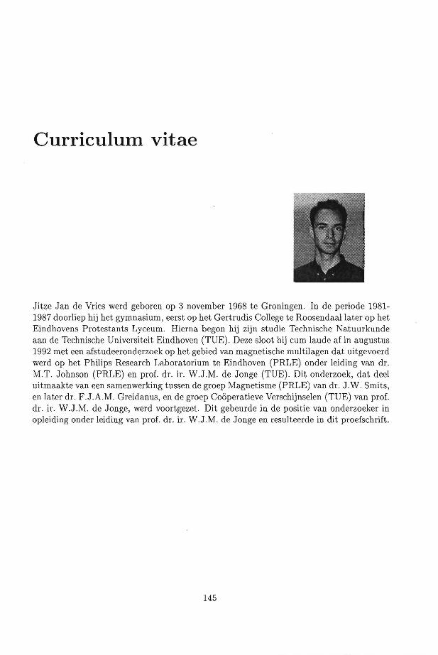
Curriculum vitae
Jitze Jan de Vries werd geboren op 3 november 1968 te Groningen. In de periode 1981-1987 doorliep hij het gymnasium, eerst op het Gertrudis College te Roosendaallater op het Eindhovens Protestants Lyceum. Hierna began hij zijn studie Technische Natuurkunde aan de Technische Universiteit Eindhoven (TUE) . Deze sloot hij cum laude af in augustus 1992 met een afstudeeronderzoek op het gebied van magnetische multilagen dat uitgevoerd werd op het Philips Research Laboratorium te Eindhoven (PRLE) onder Ieiding van dr. M.T . Johnson (PRLE) en prof. dr. ir. W.J.M. de Jonge (TUE). Dit onderzoek, dat dee! uitmaakte van een samenwerking tussen de groep Magnetisme (PRLE) van dr. J .W. Smits, en later dr. F.J.A.M. Greidanus, en de groep Cooperatieve Verschijnselen (TUE) van prof. dr. ir. W.J.M. de Jonge, werd voortgezet. Dit gebeurde in de positie van onderzoeker in opleiding onder Ieiding van prof. dr. ir. W.J.M. de Jonge en resulteerde in dit proefschrift.
145
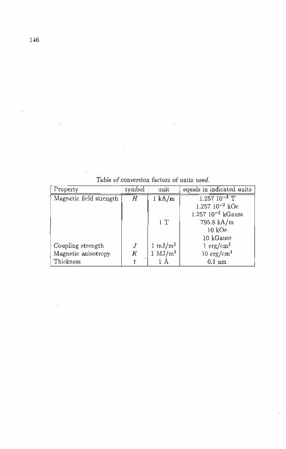
146
Table of conversion factors of units used.
I Property I symbol I unit I equals in indicated units I Magnetic field strength H 1 kA/m 1.257 10-3 T
1.257 10-2 kOe 1.257 10-2 kGauss
1 T 795.8 kA/m 10 kOe
10 kGauss Coupling strength J 1 mJ/m2 1 erg/cm2
Magnetic anisotropy K 1 MJ/m3 10 erg/cm3
Thickness t 1A 0.1 nm
Stellingen
behorende bij het proefschrift
Interlayer Exchange Coupling
in Magnetic Multilayers
A systematic study
J .J. de Vries
21 november 1996

1. De waarneming van meerdere antiferromagnetische koppelingspieken in opgedampt Co/Au(lll) toont aan dat de afwezigheid van eenzelfde waarneming in opgedampt Co/Cu(lll) een andere oorzaak heeft dan de grote hoek tussen de orientatie en de Fermisnelheid behorende bij de extremale overspanningsvector in combinatie met een roostermispassing.
Dit proefschrift: hoofdstuk 5.
2. De oscillatie van de koppelingssterkte als functie van de dikte van de magnetische laag en de afdeklaag is een van de sterkste, experimentele bewijzen voor het elektron-optische model van Bruno voor de tussenlaagkoppeling.
P. Bruno, Phys. Rev. B. 52, 411 (1995) ; Dit proefschrift: hoofdstukken 6, 7 en 8.
3. Het waargenomen verloop van de sterkte van de tussenlaagkoppeling met de dikte. van de tussenlaag in nominaal Fe/Si met een enkel antiferromagnetisch maximum, is uiterst misleidend geweest voor de interpretatie van deze dikteafhankelijkheid.
E.E. Fullerton et . al., J. Magn . Magn. Mater. 117, 1301 (1992). Dit proefschrift: hoofdstuk 9.
4. De eenvoudige empirische verklaring van de magnetische anisotropie in magnetische multilagen door middel van een grensvlakbijdrage en een volumebijdrage in vergelijking met de ingewikkelde ab initio berekeningen hieraan, doet vermoeden dat dit verschijnsel nog onvoldoende begrepen wordt.
Daalderop et al., Phys. Rev. B 42 7270, (1990); P .F . Carcia et al., Appl. Phys. Lett. 47 178 (1985).
5. Met de techniek van al of niet spinopgeloste foto-emissie, waarmee de lange oscillatieperiode voor Cu(lOO) is gemeten, is de meting van de korte oscillatieperiode voor Cu(lOO) vrijwel niet uitvoerbaar.
J .E . Ortega en F.J. Himpsel, Phys. Rev . Lett. 69, 844 (1992); C. Carbone et al., Phys. Rev. Lett . 71, 2805 (1993).
6. De toename van de magnetoweerstand wanneer dunne Co-laagjes worden aangebracht aan Nio.aFeo. 2 /Cu-grensvlakken , is geen aanwijzing dat spinafhankelijke elektronenverstrooiing overwegend plaatsvindt aan de grensvlakken, zoals door Parkin beweerd wordt, maar geeft slechts het verschil tussen de spinafhankelijke verstrooiing aan een Co/Cu- en een Nio aFeo.2 /Cugrensvlak weer.
S.S.P. Parkin, Phys. Rev. Lett . 71, 1641 (1993).
7. In principe Iran het elektrische analogon van de magnetische tussenlaagkoppeling geobserveerd word en door, bijvoorbeeld met elektro-optische effecten , de polarisatie van twee ferroelektrisch lagen gescheiden door een geleidende tussenlaag te meten als functie van het elektrische veld.
8. Er kan nog heel wat onderzoek gedaan worden aan alledaagse verschij nselen.
Y. Tanabe en K. Kaneko, Phys. Rev. Lett. 73 , 1372 (1994).
9. Recentelijk heeft de reclamewereld een nieuwe aantrekkingskracht van het magnetisme ontdekt .