Embed Size (px)
Citation preview

International Journal of Innovative Studies in Sciences and Engineering Technology
(IJISSET)
ISSN 2455-4863 (Online) www.ijisset.org Volume: 2 Issue: 12 | December 2016
© 2016, IJISSET Page 30
Bridge Monitoring System
Mr.Anand Kumar Jha
Department of Electronics & Communication (ECE), PES Institute of Technology(2010-2014), Bangalore, India.
Abstract: Bridge monitoring system is significant to
health diagnosis of bridges and flyovers. This report is
proposed and developed a novel architecture for large
span bridge monitoring. A 3-level distributed structure is
adopted in the monitoring system, which includes central
server, intelligent acquisition node and local controller.
Acquisition nodes are located across the bridge. One local
controller manages all the acquisition nodes. Every
acquisition node has 8 channels, which can sample
displacement, acceleration and strain of bridge. To get
high precision data, a 10 bits A/D converter. Compare to
the traditional method, the proposed architecture has
two features. First, the acquisition node is a smart
device based on powerful DSP processor. Signals of field
sensors are analyzed and real time compressed in the
acquisition node. Only the processing results are sent to
local controller through IEEE 802.11 wireless network.
This operation can relieve load of central server and
decrease demand of communication bandwidth. Second,
2G wireless network is utilized to provide enough
bandwidth for real-time data transmission between local
controller and central server. The intelligent monitoring
system has run on a large span bridge for six months.
Running results show that the proposed system is stable
and effective.
1. INTRODUCTION
Bridges and flyovers are critical in many regions, being
used over several decades. It is critical to have a system
to monitor the health of these bridges and report when
and where maintenance operations are needed.
Advancements in sensor technology have brought the
automated real-time bridge health monitoring system.
Many long span bridges in Korea and in Japan have
adopted this real-time health monitoring system.
However, current system uses complicated and high
cost wired network amongst sensors in the bridge and
high cost optical cable between the bridge and the
management centre, which increases the overall cost of
installation and maintenance cost of health monitoring
system. The complicated wiring also makes the
installation and repair/replacement process difficult
and expensive.
In this project an idea of bridge health monitoring
system using wireless is proposed. For short distance
(among sensors in the bridge) IEEE 802.11 wireless
communication, Zigbee is used as wireless network,
and GSM is used for long distance (between the bridge
and the management centre) data communication. This
technology can be called MBM (Monitoring Based
Maintenance) that enables the bridge maintenance
engineers monitor the condition of the bridge in real
time. The sensors installed on various parts of the
bridge monitors the bend, traffic, weight of the vehicles
etc. At any point of time if any of these parameters
cross their threshold value the communication system
informs the management centre giving an alarm for
taking precautionary measures. The complete
parameters of the bridge are taken by an ARM
processor and sent to another module which is located
in a short distance. Here the communication
established is using Zigbee that uses wireless
transmitter and receiver circuitry. The receiver module
takes the parameters from the transmitter and sends a
message with all the parameters to a database centre.
The communication established between the
intermediate module and the database centre is using
GSM technology.
Fig 1: The Humber Suspension Bridge
2. LITERATURE SURVEY
[1] Roger W. Lockhart is vice president of DATAQ
Instruments, “http://www.dataq.com/applicat/
articles/ bridge-structural-monitoring.html”
The collapse of the I-35W Mississippi River Bridge in
Minneapolis, Minnesota on August 1, 2007 was a
calamity of huge proportion. Carrying over 135,000
vehicles daily, the bridge failed during the evening rush
hour resulting in thirteen fatalities and 145 injuries.
Almost immediately plans were formulated for a
replacement bridge, which subsequently opened on
September 18, 2008. But unlike its ill-fated predecessor
the new I-35W Saint Anthony Falls Bridge is designed
with an integral state-of-the-art monitoring system that
continuously assesses bridge integrity to ensure that a
catastrophic failure will not repeat.

International Journal of Innovative Studies in Sciences and Engineering Technology
(IJISSET)
ISSN 2455-4863 (Online) www.ijisset.org Volume: 2 Issue: 12 | December 2016
© 2016, IJISSET Page 31
Fig 2: New I-35W Saint Antony Falls Bridge
[2] Peter FURTNER, Danilo DELLA CA’, Chinmoy GOSH,
“Structural Health Monitoring of Signature Bridge in
Delhi - the Bridge - Structural - Health - Monitoring -
System for the Wazirabad Bridge Project”,
http://www.brimos.com/Brimos/HTML/downloads/2
013/Fullpaper_Furtner_2013.pdf
A new cable-stayed bridge is currently under
construction across the River Yamuna in Wazirabad,
Delhi. The bridge will have a total length of 675 m, with
a main span of 251 m. Its steel-concrete composite
deck, with a total width of 35.20 m, will carry four lanes
of traffic in each direction. Its dramatic inclined steel
pylon, with a height of 154 metres, and elegant stay
cable design, will make it a particularly attractive and
imposing addition to the Wazirabad skyline.
The bridge will be equipped with a sophisticated
structural health monitoring system, supplied by a joint
venture of Mageba India, Mageba Switzerland and
Vienna Consulting Engineers.
The paper describes the purpose of the system and the
requirements it will fulfil, and presents the general
system layout, a description of the equipment and the
technical solution for data transfer. A special focus is
given to the subject of data management, which
includes the archiving, analysis and presentation of the
recorded data. In addition to the compulsory control
room devices, the system will include a user interface
which allows secure internet access to the monitoring
data and results, from any location at any time.
[3] Client of NTT Data, Implementation of bridge
monitoring system in Vietnam
With Japan facing the recent social infrastructure issue
of aging infrastructure, NTT DATA developed a solution
which remotely monitors bridges in real time to
provide valuable information for maintaining bridge
structures, and estimating the extent of structural
fatigue.
NTT DATA helped the company by implementing the
bridge monitoring system- BRIMOS with the support of
ODA (Official Development Assistance) and successfully
took the first step to expanding market share in South-
East Asia.
Challenge:
The Cau Can Tho Bridge is a newly constructed bridge
built over the Mekong Delta basin where the
foundation is naturally very soft. The client was
concerned about the possibility of adverse influences of
ground subsidence on the bridge’s foundations (such as
unexpected large-scale deformation).
The bridge is used by a particularly high number of
large vehicles carrying unusually heavy cargo as the
logistics industry in vetnam that is still under
development.
[4] Gethin Roberts , Xiaolin Meng , Michele Meo , Alan
Dodson , Emily Cosser , Emanuela Iuliano, Alan Morris
(2003), A REMOTE BRIDGE HEALTH MONITORING
SYSTEM USING COMPUTATIONAL SIMULATION AND
GPS SENSOR DATA.
The grant, entitled “A Remote Bridge Health Monitoring
System Using Computational Simulation and GPS
Sensor Data” is collaborative effort with Cranfield
University, Railtrack, W S Atkins and Pell Freischman.
The work expands and carries forward previous work
started at the University of Nottingham in 1994. The
work focuses on using kinematic GPS to create and
validate finite element models of bridges, allowing the
deflections and vibrations of the structures to be
analysed for any uncharacteristic movements.
The paper details the progress of the work to date,
including the way in which the field data gathered and
analyzed by the Nottingham group is used by the
Cranfied Group in order to assess the quality of
structures. In addition, the use of a Cyrax laser scanner
to create a finite element model of a bridge is
discussed.
[5] Chae M.J.,Yo H.S., Kim J.R, Cho M.Y, 2006, Bridge
Condition monitoring system using wireless network
(Cdma And Zigbee)
In bridge health monitoring system, sensors and ZigBee
modules are combined to be ubiquitous-node (u-node,)
which are installed on the members of bridges and
sends data to the u-gateway (ubiquitous gateway) that
sends data to themanagement center wirelessly over
CDMA technology. Based on the currently installed
sensors on Yong-Jong Bridge, total 66 locations were
carefully selected for four types of sensors.

International Journal of Innovative Studies in Sciences and Engineering Technology
(IJISSET)
ISSN 2455-4863 (Online) www.ijisset.org Volume: 2 Issue: 12 | December 2016
© 2016, IJISSET Page 32
[6] Ignacio Gonza lez, Licentiate Thesis in Structural
Engineering and Bridges Stockholm, Sweden 2011,
Study and Application of Modern Bridge Monitoring
Techniques
Railway and highway bridges are an important part of
the transport infrastructure. They represent a major
investment for society and an important part of that
investment goes to inspection and maintenance.
Bridges often constitute bottlenecks in the transport
system with few practical alternative routes. As such,
closing them for repair, inspection or replacement
entails large costs for the users. Furthermore, safety
levels in bridges are expected to be higher than in other
parts of the transport system. This comes naturally due
to the fact that failure of a bridge could have severe
consequences in material damage and human lives.
Introducing monitoring techniques in its different
forms (damage detection, traffic monitoring, reliability
assessment, etc.) can save costs by improving the
understanding of the structure, thus reducing the need
of overly safe assumptions and by granting the
possibility to get early warnings of problems that
develop.
Fig 3: A flow chart depicted for SHM system
[7] A Bridge Health Monitoring System Based on NI
Hardware and Software
Based on NI data acquisition hardware and related
software, bridge health monitoring system has been set
up. This system not only meets the functionality
requirements of the monitoring task, but also endures
the severe environmental conditions that a bridge
usually faces. This article discusses the fundamentals of
structure health monitoring (SHM) and describes how
the Shanghai JUST ONE Technology company
implements SHM on the Donghai Bridge, China's first
sea-crossing bridge.
The wide geographical area that the bridge occupies
separates the sensors with long inter-distances. Thus,
the real-time requirements inherent with many of the
measuring items call for certain advanced
synchronization technique, one that works over a large
geographical area. The traditional method by sharing
sample clock signal via coaxial cables is no longer
feasible. Global Positioning System (GPS) time
synchronization, which requires no direct connection
between the measurement subsystems, is ideal for this
situation.
Situated into China East Sea, Donghai Bridge has to
endure the erosion of the seawater, the impact of
typhoons and earthquakes, and the gradual damages
caused by the traffics on the bridge. So the measuring
system must work under hostile environmental
conditions with endurance. Also, because the
monitoring is a long-term activity, the measuring
system should be extremely reliable with minimum
maintenance. These requirements are imposed on the
whole measurement and data acquisition system.
Fig 4: Donghai Bridge, Shanghai
[8] “Structural Monitoring: Making Bridges Safer
Across the United States” (2008), Motorola Solutions
Bridge structures are key elements of the U.S. roadway
system and vital assets for the nation’s economy and
security. Their functioning is critical, but opportunities
for failure are many, including deteriorating materials,
underlying construction issues and improper load
ratings. At any given point in time, bridges may also be
threatened by natural disaster, man-made events,
defective materials or simply by long-term “wear and
tear.” Today, continuous structural health monitoring
solutions that combine embedded sensor systems with
wireless communications networks are helping to
identify potentially dangerous structures, and to
pinpoint conditions that can be repaired well before a
bridge fails.

International Journal of Innovative Studies in Sciences and Engineering Technology
(IJISSET)
ISSN 2455-4863 (Online) www.ijisset.org Volume: 2 Issue: 12 | December 2016
© 2016, IJISSET Page 33
Fig 5: Private Communication in the proposed model
3. PROBLEM DEFINITION
Flyovers and highway bridge systems are critical in
many regions, being used over several decades. It is
critical to have a system to monitor the health of these
bridges and report when and where maintenance
operations are needed. Advancements in sensor
technology have brought the automated real-time
bridge health monitoring system. However, current
system uses complicated and high cost wired network
amongst sensors in the bridge and high cost optical
cable between the bridge and the management centre.
The complicated wiring also makes the installation and
repair/replacement process difficult and expensive.
In this project an idea of bridge monitoring system
using wireless is proposed. For short distance (among
sensors in the bridge) Zigbee is used as wireless
network, and GSM is used for long distance (between
the bridge and the management centre) data
communication. This technology can be called MBM
(Monitoring Based Maintenance) that enables the
bridge maintenance engineers monitor the condition of
the bridge in real time. The sensors installed on various
parts of the bridge monitors the bend, traffic, weight of
the vehicles etc. At any point of time if any of these
parameters cross their threshold value the
communication system informs the management
centre giving an alarm for taking precautionary
measures.
The main objective of our project is to
Monitor the traffic in the bridge.
Monitor the load in the bridge.
Indicates when there are earthquakes, cracks and
bending in the bridges.
4. PROJECT OBJECTIVES
Design of Bridge monitoring system.
Analysis of bends, cracks and loads are done.
Implementation of IR sensor, Load sensor, Flex
sensor, Vibrator sensor, stepper motor. IR sensor
detects the vehicles that enter the bridge and keeps
count of the number of vehicles on the bridge. Load
sensor detects the load on the bridge. Flex sensor
detects the cracks and bending. Vibrator sensor
detects extreme vibration on the bridge. Stepper
motor acts as the gate in our bridge monitoring
system
We set up the test bed.
5. PROJECT DELIVERABLES
Algorithm for monitoring the bridge
Hardware of all the sensors.
Software for burning the code on the chip.
Firmware Development is been carried out.
Code for all sensors and monitoring the bridge.
User Manual for ARM 7 (LPC2148), GSM, and Zigbee
were referred.
6. DESIGN
6.1. System Block Diagram
Fig 6: System Block Diagram
6.2. Block Diagrams
The sensors are installed on various parts of the bridge
as shown in the above system block diagram, monitors
the bend, traffic, weight of the vehicles etc. At any point
of time if any of these parameters cross their threshold
value the communication system informs the
management centre giving an alarm for taking
precautionary measures. The complete parameters of
the bridge are taken by a ARM microcontroller and sent
to another module which is located in a short distance.
Here the communication established is using Zigbee
that uses wireless Transmitter and Receiver circuitry.
The receiver module takes the parameters from the
transmitter and sends a message with all the
parameters to a database centre. The communication
International Journal of Innovative Studies in Sciences and Engineering Technology
(IJISSET)
ISSN 2455-4863 (Online) www.ijisset.org Volume: 2 Issue: 12 | December 2016
© 2016, IJISSET Page 34
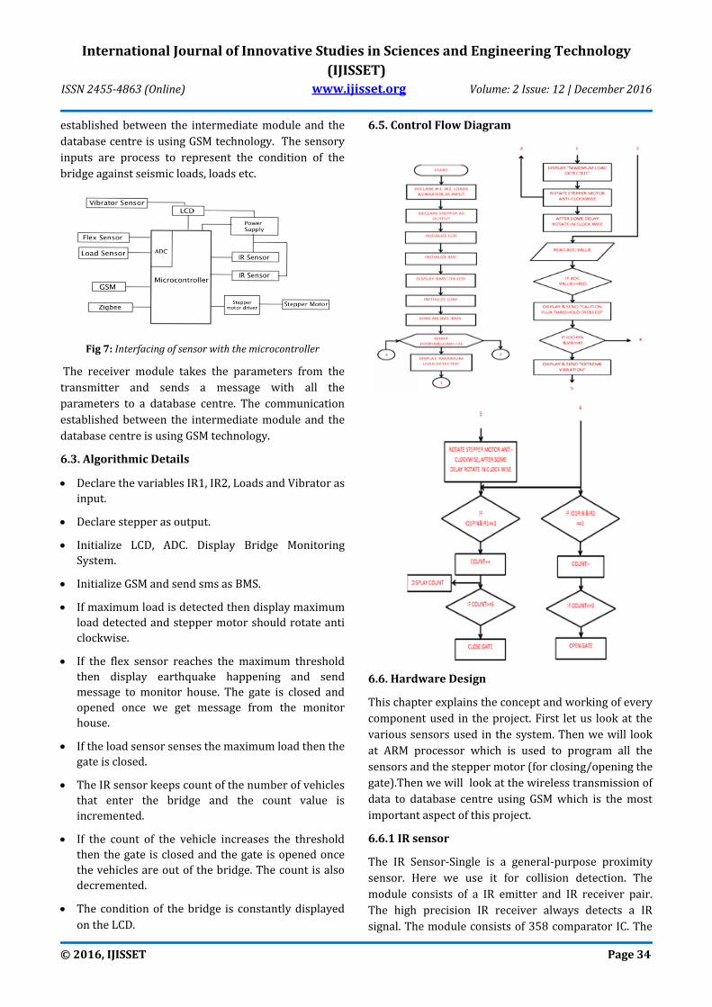
established between the intermediate module and the
database centre is using GSM technology. The sensory
inputs are process to represent the condition of the
bridge against seismic loads, loads etc.
Fig 7: Interfacing of sensor with the microcontroller
The receiver module takes the parameters from the
transmitter and sends a message with all the
parameters to a database centre. The communication
established between the intermediate module and the
database centre is using GSM technology.
6.3. Algorithmic Details
Declare the variables IR1, IR2, Loads and Vibrator as
input.
Declare stepper as output.
Initialize LCD, ADC. Display Bridge Monitoring
System.
Initialize GSM and send sms as BMS.
If maximum load is detected then display maximum
load detected and stepper motor should rotate anti
clockwise.
If the flex sensor reaches the maximum threshold
then display earthquake happening and send
message to monitor house. The gate is closed and
opened once we get message from the monitor
house.
If the load sensor senses the maximum load then the
gate is closed.
The IR sensor keeps count of the number of vehicles
that enter the bridge and the count value is
incremented.
If the count of the vehicle increases the threshold
then the gate is closed and the gate is opened once
the vehicles are out of the bridge. The count is also
decremented.
The condition of the bridge is constantly displayed
on the LCD.
6.5. Control Flow Diagram
6.6. Hardware Design
This chapter explains the concept and working of every
component used in the project. First let us look at the
various sensors used in the system. Then we will look
at ARM processor which is used to program all the
sensors and the stepper motor (for closing/opening the
gate).Then we will look at the wireless transmission of
data to database centre using GSM which is the most
important aspect of this project.
6.6.1 IR sensor
The IR Sensor-Single is a general-purpose proximity
sensor. Here we use it for collision detection. The
module consists of a IR emitter and IR receiver pair.
The high precision IR receiver always detects a IR
signal. The module consists of 358 comparator IC. The
International Journal of Innovative Studies in Sciences and Engineering Technology
(IJISSET)
ISSN 2455-4863 (Online) www.ijisset.org Volume: 2 Issue: 12 | December 2016
© 2016, IJISSET Page 35
output of sensors high whenever it IR frequency and
low otherwise. The on-board LED indicator helps user
to check status of the sensor without using any
additional hardware. The power consumption of this
module is low. It gives a digital output.
Application Ideas:
Obstacle detection
Shaft encoder
Fixed frequency detection
Fig 8: IC of IR sensor
Fig 9: Block Diagram of IR sensor
Overview of Schematic
The sensitivity of the IR Sensor is tuned using the
potentiometer. The potentiometer is tunable in both
the directions. Initially tune the potentiometer in
clockwise direction such that the indicator LED starts
glowing. Once that is achieved, turn the potentiometer
just enough in anti-clockwise direction to turn off the
Indicator LED. At this point the sensitivity of the
receiver is maximum. Thus, its sensing distance is
maximum at this point. If the sensing distance (i.e.,
Sensitivity) of the receiver is needed to be reduced,
then one can tune the potentiometer in the anti-
clockwise direction from this point.
Further, if the orientation of both Tx and Rx LED’s is
parallel to each other, such that both are facing
outwards, then their sensitivity maximum. If they are
moved away from each other, such that they are
inclined to each other at their soldered end, then their
sensitivity reduces.
Tuned sensitivity of the sensors is limited to the
surroundings. Once tuned for a particular surrounding,
they will work perfectly until the IR illumination
conditions of that region nearly constant. For example,
if the potentiometers tuned inside room/building for
maximum sensitivity and then taken out in open
sunlight, it will require retuning, since sun’s rays also
contain Infrared (IR) frequencies, thus acting as an IR
source (transmitter). This will disturb the receiver’s
sensing capacity. Hence it needs to be returned to work
perfectly in the new surroundings.
The output of IR receiver goes low when it receives IR
signal. Hence the output pin is normally low because
though the IR LED is continuously transmitting, due to
no obstacle, nothing is reflected back to the IR receiver.
The indication LED is off. When an obstacle is
encountered, the output of IR receiver goes low; IR
signal is reflected from the obstacle surface. This drives
the output of the comparator low. This output is
connected to the cathode of the LED, which then turns
ON.
6.6.2. Vibration sensor
Product Description
This sensor buffers a piezoelectric transducer. As the
transducer is displaced from the mechanical neutral
axis, bending creates strain within the piezoelectric
element and generates voltages.
Specifications
The Vibration Sensor Detector is designed for the
security practice When Vibration Sensor Alarm
recognizes movement or vibration, it sends a signal to
either control panel Developed a new type of Omni-
directional high sensitivity Security Vibration Detector
with Omni-directional detection.
Fig 3: Interfacing Vibrator Sensor

International Journal of Innovative Studies in Sciences and Engineering Technology
(IJISSET)
ISSN 2455-4863 (Online) www.ijisset.org Volume: 2 Issue: 12 | December 2016
© 2016, IJISSET Page 36
6.6.3. Load sensor
A load cell is a “load transducer” which converts the
weight or load acting on it into electrical signals. A load
cell is composed of an aluminum alloy spring element,
strain gauges (serving as sensors) and a bridge circuit.
The strain gauges themselves are bonded onto four
areas, which become considerably distorted in the
spring element. The load cell detects the force of the
distortion as voltage change.
Fig 11: Spring action in Load Sensor
Fig 12: Interfacing of Load Sensor
6.6.4. Flex sensor
Flex sensors are sensors that change in resistance
depending on the amount of bend on the sensor. They
convert the change in bend to electrical resistance - the
more the bend, the more the resistance value. They are
usually in the form of a thin strip from 1" -5" long that
vary in resistance.
Flex sensors are Analog resistors. They work as
variable Analog voltage dividers. Inside the flex sensor
are carbon sensitive elements within a thin flexible
substrate, more carbon means less resistance. When
the substrate is bent the sensor produces a resistance
output relative to the bend radius.
Fig 13: Working of Flex Sensor
Fig 14: Dimensional diagram of flex sensor
Features:
Angle Displacement Measurement
Bends and Flexes physically with motion device
Possible Uses
Robotics
Gaming (Virtual Motion)
Medical Devices
Computer Peripherals
Musical Instruments
Physical Therapy
Simple Construction
Low Profile
Mechanical Specifications
Life Cycle: >1 million
Height: 0.43mm (0.017")
Temperature Range: -35°C to +80°C
Electrical specifications
Flat Resistance: 10K Ohms
Resistance Tolerance: ±30%
Bend Resistance Range: 60K to 110K Ohms
Power Rating: 0.50 Watts continuous. 1 Watt Peak
Fabrication of flex sensor:
Fig 15: Fabrication of Flex Sensor

International Journal of Innovative Studies in Sciences and Engineering Technology
(IJISSET)
ISSN 2455-4863 (Online) www.ijisset.org Volume: 2 Issue: 12 | December 2016
© 2016, IJISSET Page 37
6.6.5. Stepper motor
Stepper motors fill a unique niche in the motor control
world. These motors are commonly used in
measurement and control applications. Sample
applications include ink jet printers, CNC machines and
volumetric pumps. Several features common to all
stepper motors make them ideally suited for these
types of applications.
These features are as follows:
1. Brushless – Stepper motors are brushless. The
commutator and brushes of conventional motors are
some of the most failure-prone components, and they
create electrical arcs that are undesirable or dangerous
in some environments.
2. Load Independent – Stepper motors will turn at a
set speed regardless of load as long as the load does not
exceed the torque rating for the motor.
3. Open Loop Positioning – Stepper motors move in
quantified increments or steps. As long as the motor
runs within its torque specification, the position of the
shaft is known at all times without the need for a
feedback mechanism.
4. Holding Torque – Stepper motors are able to hold
the shaft stationary.
5. Excellent response to start-up, stopping and
reverse.
Stepper Motor Theory of Operation:
Stepper motors provide a means for precise positioning
and speed control without the use of feedback sensors.
The basic operation of a stepper motor allows the shaft
to move a precise number of degrees each time a pulse
of electricity is sent to the motor. Since the shaft of the
motor moves only the number of degrees that it was
designed for when each pulse is delivered, you can
control the pulses that are sent and control the
positioning and speed. The rotor of the motor produces
torque from the interaction between the magnetic field
in the stator and rotor. The strength of the magnetic
fields is proportional to the amount of current sent to
the stator and the number of turns in the windings.
The stepper motor uses the theory of operation for
magnets to make the motor shaft turn a precise
distance when a pulse of electricity is provided. You
learned previously that like poles of a magnet repel and
unlike poles attract. Figure 1 shows a typical cross-
sectional view of the rotor and stator of a stepper
motor. From this diagram you can see that the stator
(stationary winding) has eight poles, and the rotor has
six poles(three complete magnets). The rotor will
require 24 pulses of electricity to move the 24 steps to
make one complete revolution. Another way to say this
is that the rotor will move precisely 15° for each pulse
of electricity that the motor receives. The number of
degrees the rotor will turn when a pulse of electricity is
delivered to the motor can be calculated by dividing the
number of degrees in one revolution of the shaft (360°)
by the number of poles (north and south) in the rotor.
In this stepper motor 360° is divided by 24 to get 15°.
When no power is applied to the motor, the residual
magnetism in the rotor magnets will cause the rotor to
detent or align one set of its magnetic poles with the
magnetic poles of one of the stator magnets. This
means that the rotor will have 24 possible detent
positions. When the rotor is in a detent position, it will
have enough magnetic force to keep the shaft from
moving to the next position. This is what makes the
rotor feel like it is clicking from one position to the next
as you rotate the rotor by hand with no power applied.
Fig 16: Working of Stepper Motor
When power is applied, it is directed to only one of the
stator pairs of windings, which will cause that winding
pair to become a magnet. One of the coils for the pair
will become the North Pole, and the other will become
the South Pole. When this occurs, the stator coil that is
the North Pole will attract the closest rotor tooth that
has the opposite polarity, and the stator coil that is the
South Pole will attract the closest rotor tooth that has
the opposite polarity. When current is flowing through
these poles, the rotor will now have a much stronger
attraction to the stator winding, and the increased
torque is called holding torque.
By changing the current flow to the next stator
winding, the magnetic field will be changed 45°. The
rotor will only move 15° before its magnetic fields will
again align with the change in the stator field. The
magnetic field in the stator is continually changed as
International Journal of Innovative Studies in Sciences and Engineering Technology
(IJISSET)
ISSN 2455-4863 (Online) www.ijisset.org Volume: 2 Issue: 12 | December 2016
© 2016, IJISSET Page 38
the rotor moves through the 24 steps to move a total of
360°.
6.6.6. Zigbee
Fig 17: Zigbee Module
CC2500 ZIGBEE Module is a transceiver module,
which provides easy to use ZIGBEE communication at
2.4Ghz. It can be used to transmit and receive data at
9600-baud rates from any standard CMOS/TTL source.
This module is a direct line in replacement for your
serial communication it requires no extra hardware
and no extra coding tot works in Half Duplex mode i.e.
it provides communication in both directions, but only
one direction at same time
Features:
Supports Multiple Baud rates (9600)
Works on ISM band (2.4 GHz)
No complex wireless connection software or
intimate knowledge of ZIGBEE is required to
connect our serial devices.
Designed to be as easy to use as cables.
No external Antenna required.
Plug and play device.
Works on 5 DC supply.
6.6.7. ARM 7 processor
Fig 18: LPC2148 controller board (with ARM 7 processor)
ARM Board-LPC214X is a breakout board for LPC2148
ARM7TMDI based microcontroller. The LPC2148
microcontroller has 512KB of internal flash and 32+8K
RAM. Following are the salient features of the board.
Two layer PCB (FR-4 material)
Power: USB powered
ISP and reset switch
Test LED
32Khz crystal for RTC
Connectors:
Extension headers for all microcontroller pins
1 RS232 connector for ISP
USB B-type connector with Link-LED
20pin - JTAG connector
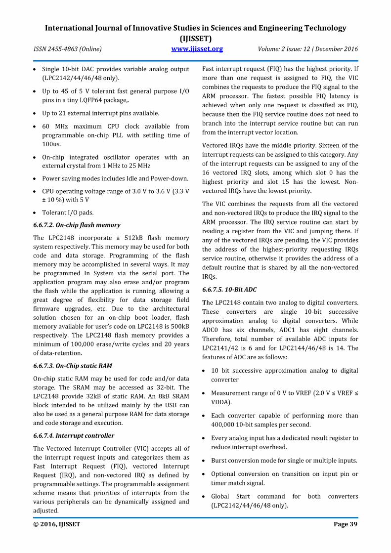
Fig 19: Pin Diagram of ARM7 processor
6.6.7.1. Features
16-bit/32-bit ARM7TDMI-S microcontroller in a tiny
LQFP64 package.
8kB to 40kB of on-chip static RAM and 32kB to
512kB of on-chip flash memory.
128-bit wide interface/accelerator enables high-
speed 60 MHz operation.
USB 2.0 Full-speed compliant device controller with
2kB of endpoint RAM. In addition, the LPC2146/48
provides 8kB of on-chip RAM accessible to USB by
DMA.
One or two (LPC2141/42 vs. LPC2144/46/48) 10-
bit ADCs provide a total of
6/14 analog inputs, with conversion times as low as
2.44us per channel.
International Journal of Innovative Studies in Sciences and Engineering Technology
(IJISSET)
ISSN 2455-4863 (Online) www.ijisset.org Volume: 2 Issue: 12 | December 2016
© 2016, IJISSET Page 39
Single 10-bit DAC provides variable analog output
(LPC2142/44/46/48 only).
Up to 45 of 5 V tolerant fast general purpose I/O
pins in a tiny LQFP64 package,.
Up to 21 external interrupt pins available.
60 MHz maximum CPU clock available from
programmable on-chip PLL with settling time of
100us.
On-chip integrated oscillator operates with an
external crystal from 1 MHz to 25 MHz
Power saving modes includes Idle and Power-down.
CPU operating voltage range of 3.0 V to 3.6 V (3.3 V
± 10 %) with 5 V
Tolerant I/O pads.
6.6.7.2. On-chip flash memory
The LPC2148 incorporate a 512kB flash memory
system respectively. This memory may be used for both
code and data storage. Programming of the flash
memory may be accomplished in several ways. It may
be programmed In System via the serial port. The
application program may also erase and/or program
the flash while the application is running, allowing a
great degree of flexibility for data storage field
firmware upgrades, etc. Due to the architectural
solution chosen for an on-chip boot loader, flash
memory available for user’s code on LPC2148 is 500kB
respectively. The LPC2148 flash memory provides a
minimum of 100,000 erase/write cycles and 20 years
of data-retention.
6.6.7.3. On-Chip static RAM
On-chip static RAM may be used for code and/or data
storage. The SRAM may be accessed as 32-bit. The
LPC2148 provide 32kB of static RAM. An 8kB SRAM
block intended to be utilized mainly by the USB can
also be used as a general purpose RAM for data storage
and code storage and execution.
6.6.7.4. Interrupt controller
The Vectored Interrupt Controller (VIC) accepts all of
the interrupt request inputs and categorizes them as
Fast Interrupt Request (FIQ), vectored Interrupt
Request (IRQ), and non-vectored IRQ as defined by
programmable settings. The programmable assignment
scheme means that priorities of interrupts from the
various peripherals can be dynamically assigned and
adjusted.
Fast interrupt request (FIQ) has the highest priority. If
more than one request is assigned to FIQ, the VIC
combines the requests to produce the FIQ signal to the
ARM processor. The fastest possible FIQ latency is
achieved when only one request is classified as FIQ,
because then the FIQ service routine does not need to
branch into the interrupt service routine but can run
from the interrupt vector location.
Vectored IRQs have the middle priority. Sixteen of the
interrupt requests can be assigned to this category. Any
of the interrupt requests can be assigned to any of the
16 vectored IRQ slots, among which slot 0 has the
highest priority and slot 15 has the lowest. Non-
vectored IRQs have the lowest priority.
The VIC combines the requests from all the vectored
and non-vectored IRQs to produce the IRQ signal to the
ARM processor. The IRQ service routine can start by
reading a register from the VIC and jumping there. If
any of the vectored IRQs are pending, the VIC provides
the address of the highest-priority requesting IRQs
service routine, otherwise it provides the address of a
default routine that is shared by all the non-vectored
IRQs.
6.6.7.5. 10-Bit ADC
The LPC2148 contain two analog to digital converters.
These converters are single 10-bit successive
approximation analog to digital converters. While
ADC0 has six channels, ADC1 has eight channels.
Therefore, total number of available ADC inputs for
LPC2141/42 is 6 and for LPC2144/46/48 is 14. The
features of ADC are as follows:
10 bit successive approximation analog to digital
converter
Measurement range of 0 V to VREF (2.0 V ≤ VREF ≤
VDDA).
Each converter capable of performing more than
400,000 10-bit samples per second.
Every analog input has a dedicated result register to
reduce interrupt overhead.
Burst conversion mode for single or multiple inputs.
Optional conversion on transition on input pin or
timer match signal.
Global Start command for both converters
(LPC2142/44/46/48 only).

International Journal of Innovative Studies in Sciences and Engineering Technology
(IJISSET)
ISSN 2455-4863 (Online) www.ijisset.org Volume: 2 Issue: 12 | December 2016
© 2016, IJISSET Page 40
6.6.7.6. UARTs
The LPC2148 each contain two UARTs. In addition to
standard transmit and receive data lines, the LPC2148
UART1 also provides a full modem control handshake
interface. Compared to previous LPC2000
microcontrollers, UARTs in LPC2148 introduce a
fractional baud rate generator for both UARTs, enabling
these microcontrollers to achieve standard baud rates
such as 115200 with any crystal frequency above 2
MHz In addition, auto-CTS/RTS flow-control functions
are fully implemented in hardware (UART1 in
LPC2144/46/48 only). The features are as follows:
16 byte Receive and Transmit FIFOs.
Register locations conform to ‘550 industry
standard.
Receiver FIFO trigger points at 1, 4, 8, and 14 bytes
Built-in fractional baud rate generator covering
wide range of baud rates without a need for external
crystals of particular values.
Transmission FIFO control enables implementation
of software (XON/XOFF) flow control on both
UARTs.
LPC2144/46/48 UART1 equipped with standard
modem interface signals. This
Module also provides full support for hardware flow
control (auto-CTS/RTS).
6.6.7.7. System control
Crystal Oscillator:
On-chip integrated oscillator operates with external
crystal in range of 1 MHz to 25 MHz The oscillator
output frequency is called fosc and the ARM processor
clock frequency is referred to as CCLK for purposes of
rate equations, etc. fosc and CCLK are the same value
unless the PLL is running and connected.
PLL (Phase Locked Loop):
The PLL accepts an input clock frequency in the range
of 10 MHz to 25 MHz The Input frequency is multiplied
up into the range of 10 MHz to 60 MHz with a Current
Controlled Oscillator (CCO). The multiplier can be an
integer value from 1 to 32 (in practice, the multiplier
value cannot be higher than 6 on this family of
microcontrollers due to the upper frequency limit of
the CPU). The CCO operates in the range of 156 MHz to
320 MHz, so there is an additional divider in the loop to
keep the CCO within its frequency range while the PLL
is providing the desired output frequency. The output
divider may be set to divide by 2, 4, 8, or 16 to produce
the output clock. Since the minimum output divider
value is 2, it is insured that the PLL output has a 50 %
duty cycle. The PLL is turned off and bypassed
following a chip reset and may be enabled by software.
The program must configure and activate the PLL, wait
for the PLL to Lock, then connect to the PLL as a clock
source. The PLL settling time is 100us.
Reset and wake up timer:
Reset has two sources on the LPC2148: the RESET pin
and watchdog reset. The RESET pin is a Schmitt trigger
input pin with an additional glitch filter. Assertion of
chip reset by any source starts the Wake-up Timer (see
Wake-up Timer description below), causing the
internal chip reset to remain asserted until the external
reset is de-asserted, the oscillator is running, a fixed
number of clocks have passed, and the on-chip flash
controller has completed its initialization.
When the internal reset is removed, the processor
begins executing at address 0, which is the reset vector.
At that point, all of the processor and peripheral
registers have been initialized to predetermined values.
The Wake-up Timer ensures that the oscillator and
other analog functions required for chip operation are
fully functional before the processor is allowed to
execute instructions. This is important at power on, all
types of reset, and whenever any of the aforementioned
functions are turned off for any reason. Since the
oscillator and other functions are turned off during
Power-down mode, any wake-up of the processor from
Power-down mode makes use of the Wake-up Timer.
The Wake-up Timer monitors the crystal oscillator as
the means of checking whether it Is safe to begin code
execution. When power is applied to the chip, or some
event caused the chip to exit Power-down mode, some
time is required for the oscillator to produce a signal of
sufficient amplitude to drive the clock logic. The
amount of time depends on many factors, including the
rate of VDD ramp (in the case of power on), the type of
crystal and its electrical characteristics (if a quartz
crystal is used), as well as any other external circuitry
(e.g. capacitors), and the characteristics of the oscillator
itself under the existing ambient conditions.
External interrupt inputs
The LPC2148 include up to nine edge or level sensitive
External Interrupt Inputs as selectable pin functions.
When the pins are combined, external events can be

International Journal of Innovative Studies in Sciences and Engineering Technology
(IJISSET)
ISSN 2455-4863 (Online) www.ijisset.org Volume: 2 Issue: 12 | December 2016
© 2016, IJISSET Page 41
processed as four independent interrupt signals. The
External Interrupt Inputs can optionally be used to
wake-up the processor from Power-down mode.
Additionally capture input pins can also be used as
external interrupts without the Option to wake the
device up from Power-down mode.
6.6.7.8. Emulation and debugging
The LPC2148 support emulation and debugging via a
JTAG serial port. A trace port allows tracing program
execution. Debugging and trace functions are
multiplexed only with GPIOs on Port 1. This means that
all communication, timer and interface peripherals
residing on Port 0 are available during the
development and debugging phase as they are when
the application is run in the embedded system itself.
6.6.8. GSM module
6.6.8.1. Introduction
The GSM Modem comes with a serial interface through
which the modem can be controlled using AT command
interface. An antenna and a power adapter are
provided. The basic segregation of working of the
modem is as under:
Voice calls
SMS
GSM Data calls
GPRS
Voice calls
Voice calls are not an application area to be targeted. In
future if interfaces like a microphone and speaker are
provided for some applications then this can be
considered.
SMS
SMS is an area where the modem can be used to
provide features like: Pre-stored SMS transmission.
These SMS can be transmitted on certain trigger events
in an automation system. SMS can also be used in areas
where small text information has to be sent. The
transmitter can be an automation system or machines
like vending machines, collection machines or
applications like positioning systems where the
navigator keeps on sending SMS at particular time
intervals. SMS can be a solution where GSM data call or
GPRS services are not available.
GSM data calls
Data calls can be made using this modem. Data calls can
be made to a normal PSTN modem/phone line also
(even received). Data calls are basically made to
send/receive data streams between two units either
PC’s or embedded devices. The advantage of Data calls
over SMS is that both parties are capable of
sending/receiving data through their terminals.
Applications and facts about GSM data calls
Devices that have communication on serial port
either on PC or in the embedded environment
Devices that want to communicate with a remote
server for data transfer
This capability of data transfer can help in reducing
processing requirements of the device
The basic aim is to provide a wireless solution
keeping the existing firmware intact
The clients firmware continues to work without any
modifications (no changes in the existing software
required)
GSM data calls can be a good solution where data
has to be transmitted from a hand-held device to a
central server
The interface on two sides can be between PC’s as
well as embedded devices
Calls can be established by the terminals at either
side to start data calls
The Modem remains transparent during data
transfer after the call is established.
Call establishment utility to be provided in case PC
terminals
Call establishment to be automated in case of
embedded terminals. GSM converter can be an
option where intelligence of establishing calls has to
be put in case of embedded devices. Concept of GSM
converter is discussed
Dial-up networks using GSM data calls
Dial up networking is a utility available with Windows
through a person can dial the Data call number of this
modem from any PC and share the file system on either
PC’s. This can be a good utility where both terminals
are PC based. Sharing the file system remotely enables
monitoring of devices remotely. Thus the modem can
act as a piece of device which acts as a spy in the
system. Can be a good debugging utility wherein a
person can configure/monitor a remote PC based
system and even rectify it. Some companies do sell
International Journal of Innovative Studies in Sciences and Engineering Technology
(IJISSET)
ISSN 2455-4863 (Online) www.ijisset.org Volume: 2 Issue: 12 | December 2016
© 2016, IJISSET Page 42
their products with a GSM modem inside it just for this
handy feature which allows them to configure the
machines sitting anywhere in the world.
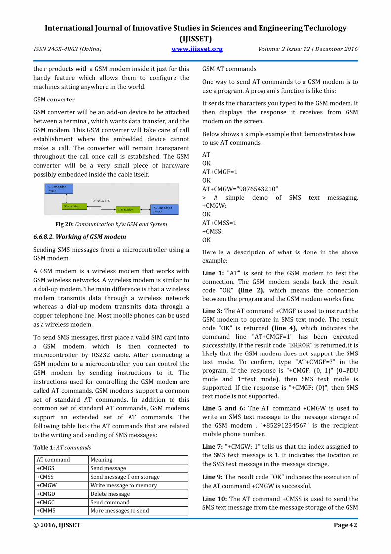
GSM converter
GSM converter will be an add-on device to be attached
between a terminal, which wants data transfer, and the
GSM modem. This GSM converter will take care of call
establishment where the embedded device cannot
make a call. The converter will remain transparent
throughout the call once call is established. The GSM
converter will be a very small piece of hardware
possibly embedded inside the cable itself.
Fig 20: Communication b/w GSM and System
6.6.8.2. Working of GSM modem
Sending SMS messages from a microcontroller using a
GSM modem
A GSM modem is a wireless modem that works with
GSM wireless networks. A wireless modem is similar to
a dial-up modem. The main difference is that a wireless
modem transmits data through a wireless network
whereas a dial-up modem transmits data through a
copper telephone line. Most mobile phones can be used
as a wireless modem.
To send SMS messages, first place a valid SIM card into
a GSM modem, which is then connected to
microcontroller by RS232 cable. After connecting a
GSM modem to a microcontroller, you can control the
GSM modem by sending instructions to it. The
instructions used for controlling the GSM modem are
called AT commands. GSM modems support a common
set of standard AT commands. In addition to this
common set of standard AT commands, GSM modems
support an extended set of AT commands. The
following table lists the AT commands that are related
to the writing and sending of SMS messages:
Table 1: AT commands
AT command Meaning
+CMGS Send message
+CMSS Send message from storage
+CMGW Write message to memory
+CMGD Delete message
+CMGC Send command
+CMMS More messages to send
GSM AT commands
One way to send AT commands to a GSM modem is to
use a program. A program's function is like this:
It sends the characters you typed to the GSM modem. It
then displays the response it receives from GSM
modem on the screen.
Below shows a simple example that demonstrates how
to use AT commands.
AT
OK
AT+CMGF=1
OK
AT+CMGW="9876543210"
> A simple demo of SMS text messaging.
+CMGW:
OK
AT+CMSS=1
+CMSS:
OK
Here is a description of what is done in the above
example:
Line 1: "AT" is sent to the GSM modem to test the
connection. The GSM modem sends back the result
code "OK" (line 2), which means the connection
between the program and the GSM modem works fine.
Line 3: The AT command +CMGF is used to instruct the
GSM modem to operate in SMS text mode. The result
code "OK" is returned (line 4), which indicates the
command line "AT+CMGF=1" has been executed
successfully. If the result code "ERROR" is returned, it is
likely that the GSM modem does not support the SMS
text mode. To confirm, type "AT+CMGF=?" in the
program. If the response is "+CMGF: (0, 1)" (0=PDU
mode and 1=text mode), then SMS text mode is
supported. If the response is "+CMGF: (0)", then SMS
text mode is not supported.
Line 5 and 6: The AT command +CMGW is used to
write an SMS text message to the message storage of
the GSM modem . "+85291234567" is the recipient
mobile phone number.
Line 7: "+CMGW: 1" tells us that the index assigned to
the SMS text message is 1. It indicates the location of
the SMS text message in the message storage.
Line 9: The result code "OK" indicates the execution of
the AT command +CMGW is successful.
Line 10: The AT command +CMSS is used to send the
SMS text message from the message storage of the GSM

International Journal of Innovative Studies in Sciences and Engineering Technology
(IJISSET)
ISSN 2455-4863 (Online) www.ijisset.org Volume: 2 Issue: 12 | December 2016
© 2016, IJISSET Page 43
modem. "1" is the index of the SMS text message
obtained from line 7.
Line 11: "+CMSS: 20" tells us that the reference
number assigned to the SMS text message is 20.
Line 13: The result code "OK" indicates the execution
of the AT command +CMSS are successful.
By using the above procedure message is sent by the
GSM modem.
6.6.8.3. Characteristics of GSM standard:
Fully digital system using 900,1800 MHz frequency
band.
TDMA over radio carriers (200 KHz carrier spacing.
8 full rate or 16 half-rate TDMA channels per
carrier.
User/terminal authentication for fraud control.
Encryption of speech and data transmission over
the radio path.
Full international roaming capability.
Low speed data services (up to 9.6 Kb/s).
Compatibility with ISDN.
Support of Short Message Service (SMS).
6.6.8.4. Advantages of GSM over analog system:
Capacity increases.
Reduced RF transmission power and longer battery
life.
International roaming capability.
Better security against fraud (through terminal
validation and user authentication).
Encryption capability for information security and
privacy.
Compatibility with ISDN, leading to wider range of
service.
6.6.9. Liquid crystal display
6.6.9.1. Introduction
An LCD is a small low cost display. It is easy to interface
with a micro-controller because of an embedded
controller (the black blob on the back of the board).
This controller is standard across many displays (HD
44780), which means many micro-controllers
(including the Arduino) have libraries that make
displaying messages as easy as a single line of code.
Hence it is very important device in embedded system.
It offers high flexibility to user as he can display the
required data on it
Major task in LCD interfacing is the initialization
sequence. In LCD initialization you have to send
command bytes to LCD. Set the interface mode, display
mode, address counter increment direction, set
contrast of LCD, horizontal or vertical addressing mode,
color format. This sequence is given in respective LCD
driver datasheet. Studying the function set of LCD lets
you know the definition of command bytes. It varies
from one LCD to another.
Next step after initialization is to send data bytes to
required display data RAM memory location. Firstly set
the address location using address set command byte
and than send data bytes using the DDRAM write
command. To address specific location in display data
RAM one must have the knowledge of how the address
counter is incremented.
6.6.9.3. Connections
A 14 pin access is provided having 8 data lines,3
control lines and 3 power lines. The function of each of
the connections is shown in table 4.7.
Pin 1 and 2 are the power supply lines, VSS and VDD.
The VDD pin should be connected to positive supply
and VSS to 0V supply or ground. Although the LCD
module data sheets specify a 5V DC supply. Supplies of
6V and 4-5V both work well, and even 3V is sufficient
for some modules.
Pin 3 is a control pin, VEE, which is used to alter the
contrast of the display. Ideally, this pin should be
connected to a variable voltage supply.
Pin 4 is the (RS) register select line. When this line is
low, data bytes transferred to the display are treated as
commands and data bytes read from the display
indicate its status.
By setting the RS line high, character data can be
transferred to and from the module.
Pin 5 is read/write line. This line is pulled low in order
to write commands or character data to the module, or
pulled high to read character data or status information
from its registers.
Pin 6 is the enable line. This input is used to initiate the
actual transfer of commands or character data between
the module and the data lines. When writing to the
International Journal of Innovative Studies in Sciences and Engineering Technology
(IJISSET)
ISSN 2455-4863 (Online) www.ijisset.org Volume: 2 Issue: 12 | December 2016
© 2016, IJISSET Page 44
display, data is transferred only on high to low
transition of this signal.
Pin 7 to 14 are data bus lines (D0 to D7). Data can be
transferred to and from the display either as a single 8-
bit byte or two 4 bit nibbles. The other two pins LED+
and LED- is used for back light of the LCD.
Table 2: Pin Details on an LCD module
6.6.9.4. Interfacing LCD with microcontroller
Interfacing LCD with microcontroller is very easy task.
You just have to know the proper LCD programming
algorithm. LCD used here has HD44780u dot matrix
LCD controller. LCD module has 8-bit data interface and
control pins. One can send data as 8-bit or in pair of
two 4-bit nibbles.
To display any character on LCD micro controller has to
send its ASCII value to the data bus of LCD. For e.g. to
display 'AB' microcontroller has to send two hex bytes
41h and 42h respectively. LCD display used here is
having 16x2 size. It means 2 lines each with 16
characters.
6.6.9.5. LCD initialization
This is the pit fall for beginners. Proper working of LCD
depend on the how the LCD is initialized. We have to
send few command bytes to initialize the LCD. Simple
steps to initialize the LCD
1. Specify function set: Send 38H for 8-bit, double line
and 5x7 dot character format.
2. Display On-Off control: Send 0FH for display and
blink cursor on.
3. Entry mode set: Send 06H for cursor in increment
position and shift is invisible.
4. Clear display: Send 01H to clear display and return
cursor to home position.
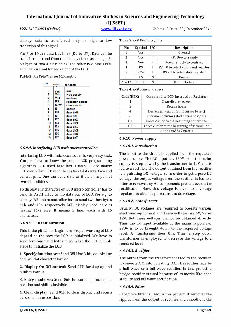
Table 3: LCD Pin Description
Pin Symbol I/O Description
1 Vss - Ground
2 Vcc - +5V Power Supply
3 Vee - Power Supply to contrast
4 RS I RS = 0 to select command register
5 R/W I RS = 1 to select data register
6 EN I/O Enable
7 to 14 D0 to D8 I/O 8 bit data bus
Table 4: LCD command codes
Code(HEX) Command to LCD Instruction Register
1 Clear display screen
2 Return home
4 Decrement cursor (shift cursor to left)
6 Increment cursor (shift cursor to right)
80 Force cursor to the beginning of first line
C0 Force cursor to the beginning of second line
2 lines and 5x7 matrix
6.6.10. Power supply
6.6.10.1. Introduction
The input to the circuit is applied from the regulated
power supply. The AC input i.e., 230V from the mains
supply is step down by the transformer to 12V and is
fed to a rectifier. The output obtained from the rectifier
is a pulsating DC voltage. So in order to get a pure DC
voltage, the output voltage from the rectifier is fed to a
filter to remove any AC components present even after
rectification. Now, this voltage is given to a voltage
regulator to obtain a pure constant dc voltage.
6.6.10.2. Transformer
Usually, DC voltages are required to operate various
electronic equipment and these voltages are 5V, 9V or
12V. But these voltages cannot be obtained directly.
Thus the a.c input available at the mains supply i.e.,
230V is to be brought down to the required voltage
level. A transformer does this. Thus, a step down
transformer is employed to decrease the voltage to a
required level.
6.6.10.3. Rectifier
The output from the transformer is fed to the rectifier.
It converts A.C. into pulsating. D.C. The rectifier may be
a half wave or a full wave rectifier. In this project, a
bridge rectifier is used because of its merits like good
stability and full wave rectification.
6.6.10.4. Filter
Capacitive filter is used in this project. It removes the
ripples from the output of rectifier and smoothens the

International Journal of Innovative Studies in Sciences and Engineering Technology
(IJISSET)
ISSN 2455-4863 (Online) www.ijisset.org Volume: 2 Issue: 12 | December 2016
© 2016, IJISSET Page 45
D.C. Output received from this filter is constant until
the mains voltage and load is maintained constant.
However, if either of the two is varied, D.C. voltage
received at this point changes. Therefore a regulator is
applied at the output stage.
6.6.10.5. Voltage regulator
As the name itself implies, it regulates the input applied
to it. A voltage regulator is an electrical regulator
designed to automatically maintain a constant voltage
level. In this project, power supply of 5V and 12V are
required. In order to obtain these voltage levels, 7805
and 7812 voltage regulators are to be used. The first
number 78 represents positive supply and the numbers
05, 12 represent the required output voltage levels.A
variable regulated power supply, also called a variable
bench power supply, is one where you can
continuously adjust the output voltage to your
requirements. Varying the output of the power supply
is the recommended way to test a project after having
double checked parts placement against circuit
drawings and the parts placement guide.
The LM7805 is simple to use. You simply connect the
positive lead of your unregulated. DC power supply
(anything from 9VDC to 24VDC) to the Input pin,
connect the negative lead to the Common pin and then
when you turn on the power, you get a 5 volt supply
from the Output pin.
6.6.10.6. Circuit features
Brief description of operation: Gives out well
regulated +5V output, output current capability of
100 mA
Circuit protection: Built-in overheating protection
shuts down output when regulator IC gets too hot.
Circuit complexity: Very simple and easy to build.
Circuit performance: Very stable +5V output
voltage, reliable operation.
Availability of components: Easy to get, uses only
very common basic components.
Applications: Part of electronics devices, small
laboratory power supplies.
Power supply voltage: Unregulated DC 8-18V
power supply.
Power supply current: Needed output current + 5
mA.
Component costs: Few dollars for the electronics
components + the input transformer.
6.8 Code Layout
7. TOOLS AND TECHNIQUES
7.1. Introduction to keilµVision3
The µVision3 IDE is a Windows-based software
development platform that combines a robust editor,
project manager, and make facility. µVision3 integrates
all tools including the C compiler, macro assembler,
linker/locator, and HEX file generator. The µVision3
IDE offers numerous features and advantages that help
you quickly and successfully develop embedded
applications. They are easy to use and are guaranteed
to help you achieve your design goals.
7.1.1. Features
The µVision3 Simulator is the only debugger that
completely simulates all on-chip peripherals.
Simulation capabilities may be expanded using the
Advanced Simulation Interface (AGSI).
µVision3 incorporates project manager, editor, and
debugger in a single environment.
The µVision3 Device Database automatically
configures the development tools for the target
microcontroller.
The µVision3 IDE integrates additional third-party
tools like VCS, CASE, and FLASH/Device
Programming.
The ULINK USB-JTAG Adapter supports both
Debugging and Flash programming with
configurable algorithm files.
Identical Target Debugger and Simulator User
Interface.
The Code Coverage feature of the µVision3
Simulator provides statistical analysis of your
program's execution.

International Journal of Innovative Studies in Sciences and Engineering Technology
(IJISSET)
ISSN 2455-4863 (Online) www.ijisset.org Volume: 2 Issue: 12 | December 2016
© 2016, IJISSET Page 46
Fig 23: Keil Window
7.1.2. Software development cycle
When you use the Keil µVision3, the project
development cycle is roughly the same as it is for any
other software development project.
Create a project, select the target chip from the
device database, and configure the tool settings.
Create source files in C or assembly.
Correct errors in source files.
Test the linked application.
The following block diagram illustrates the complete
µVision3 software development cycle. Each component
is described below.
Fig 24: Software Development Cycle using Keil uVision3
7.1.3. µVision3 IDE
The µVision3 IDE combines project management, a
rich-featured editor with interactive error correction,
option setup, makes facility, and on-line help. Use
µVision3 to create your source files and organize them
into a project that defines your target application.
µVision3 automatically compiles, assembles, and links
your embedded application and provides a single focal
point for your development efforts.
7.2. Flash magic
Flash Magic is Windows software that allows easy
access to all the ISP features provided by the devices.
Flash Magic provides a clear and simple user interface
while Erasing /Programming / Reading Flash memory
Under Windows, only one application may have access
the COM Port at any one time, Flash Magic only obtains
access to the selected COM Port when ISP operations
are being performed. Hence applications that need to
use the COM Port, such as debugging tools, may be used
while flash magic is loaded.
7.3. Embedded C
When designing software for a smaller embedded
system with the 8051, it is very commonplace to
develop the entire product using assembly code. With
many projects, this is a feasible approach since the
amount of code that must be generated is typically less
than 8 kilobytes and is relatively simple in nature. If a
hardware engineer is tasked with designing both the
hardware and the software, he or she will frequently be
tempted to write the software in assembly language.
The trouble with projects done with assembly code can
is that they can be difficult to read and maintain,
especially if they are not well commented. Additionally,
the amount of code reusable from a typical assembly
language project is usually very low. Use of a higher-
level language like C can directly address these issues.
A program written in C is easier to read than an
assembly program.
Since a C program possesses greater structure, it is
easier to understand and maintain. Because of its
modularity, a C program can better lend itself to reuse
of code from project to project. The division of code
into functions will force better structure of the
software and lead to functions that can be taken from
one project and used in another, thus reducing overall
development time. A high order language such as C
allows a developer to write code, which resembles a
human’s thought process more closely than does the
equivalent assembly code. The developer can focus
more time on designing the algorithms of the system
rather than having to concentrate on their individual
implementation. This will greatly reduce development
time and lower debugging time since the code is more
understandable.
By using a language like C, the programmer does not
have to be intimately familiar with the architecture of
the processor. This means that someone new to a given
processor can get a project up and running quicker,
since the internals and organization of the target
International Journal of Innovative Studies in Sciences and Engineering Technology
(IJISSET)
ISSN 2455-4863 (Online) www.ijisset.org Volume: 2 Issue: 12 | December 2016
© 2016, IJISSET Page 47
processor do not have to be learned. Additionally, code
developed in C will be more portable to other systems
than code developed in assembly. Many target
processors have C compilers available, which support
ANSI C.
All of this is not to say that assembly language does not
have its place. In fact, many embedded systems
(particularly real time systems) have a combination of
C and assembly code. For time critical operations,
assembly code is frequently the only way to go. One of
the great things about the C language is that it allows
you to perform low-level manipulations of the
hardware if need be, yet provides you the functionality
and abstraction of a higher order language.
8. RESULTS AND DISCUSSIONS
Fig 25: The components of the Bridge Monitoring System
Fig 26: Implemented Bridge monitoring system
Fig 27: The outputs of LCD
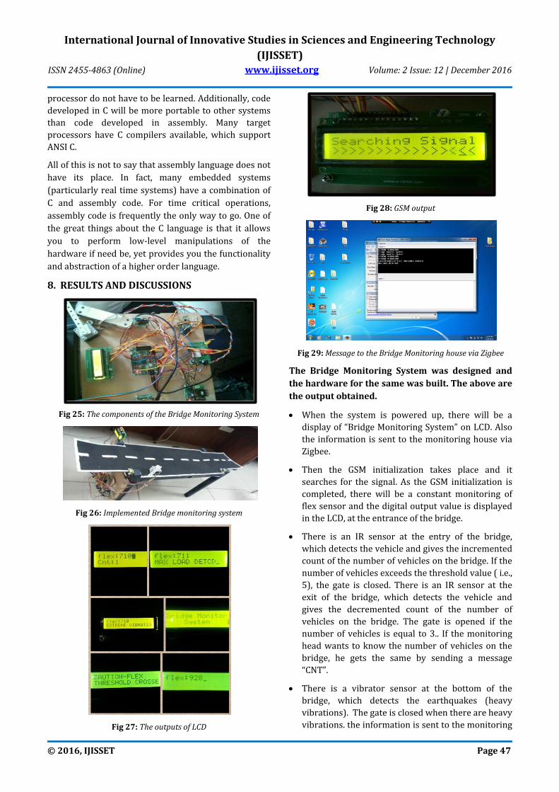
Fig 28: GSM output
Fig 29: Message to the Bridge Monitoring house via Zigbee
The Bridge Monitoring System was designed and
the hardware for the same was built. The above are
the output obtained.
When the system is powered up, there will be a
display of “Bridge Monitoring System” on LCD. Also
the information is sent to the monitoring house via
Zigbee.
Then the GSM initialization takes place and it
searches for the signal. As the GSM initialization is
completed, there will be a constant monitoring of
flex sensor and the digital output value is displayed
in the LCD, at the entrance of the bridge.
There is an IR sensor at the entry of the bridge,
which detects the vehicle and gives the incremented
count of the number of vehicles on the bridge. If the
number of vehicles exceeds the threshold value ( i.e.,
5), the gate is closed. There is an IR sensor at the
exit of the bridge, which detects the vehicle and
gives the decremented count of the number of
vehicles on the bridge. The gate is opened if the
number of vehicles is equal to 3.. If the monitoring
head wants to know the number of vehicles on the
bridge, he gets the same by sending a message
“CNT”.
There is a vibrator sensor at the bottom of the
bridge, which detects the earthquakes (heavy
vibrations). The gate is closed when there are heavy
vibrations. the information is sent to the monitoring
International Journal of Innovative Studies in Sciences and Engineering Technology
(IJISSET)
ISSN 2455-4863 (Online) www.ijisset.org Volume: 2 Issue: 12 | December 2016
© 2016, IJISSET Page 48
house via Zigbee and the monitoring head via GSM.
In order to open the gate, “K” command has to be
sent by the monitoring house.
There is a flex sensor beneath the bridge, which
detects the cracks and bending. The gate is closed
when the threshold value of flex exceeds 810. The
information is sent to the monitoring house via
Zigbee and the monitoring head via GSM. In order to
open the gate, “K” command has to be sent by the
monitoring house.
There is a load sensor at the entry of the bridge,
which detects the load on the bridge. The gate is
closed when there are heavy loads. The information
is sent to the monitoring house via Zigbee and the
monitoring head via GSM. In order to open the gate,
“K” command has to be sent by the monitoring
house.
9. CONCLUSIONS AND SCOPE FOR FUTURE
SCOPE
9.1. Conclusions
Even in developed nations like USA, it has been
found that more than one out of every four bridges
are structurally deficient.
This wireless technology could avert the kind of
bridge collapse that killed 13 and injured 145 along
Minneapolis on Aug. 1, 2007 at one-hundredth the
cost of current wired systems.
This system can help in monitoring the bridge in an
efficient, cost effective and reliable manner.
The immediacy, low cost, low energy and compact
size add up to a revolution in bridge safety
monitoring, providing a heightened level of early-
warning capability.
9.2. Future Work
Web camera can be fitted so that the density of the
vehicles can be know by the people who enter the
bridge. This can be done using MATLAB.
Instead of using IR sensor, we can use UV sensor
and more advanced sensor, which has high
sensitivity.
This project can be implemented in a two-way road
bridges. But the complexity of the project increases.
ACKNOWLEDMENTS
Studying Bachelors at P E S Institute of Technology has
been a great experience for us. We have learnt a lot
from this experience, especially to build oneself
individually. Though we have taken efforts in this
project, it would not have been successful without the
kind support and help of many individuals of PESIT. We
would like to extend our sincere thanks to all of them.
We are highly indebted to Mr. Arun Vikas Singh, Dr. T.
S. Chandar, Mrs. Deepa Yagain, Mr. Akshay Gopal, Mr.
Purushotham U. and Mrs. Ashwini Bhat for their
guidance and constant supervision as well as for
providing necessary information regarding the project
& also for their support in completing the project. We
specially thank Mrs. Rajeshwari B. A. for her constant
guidance for providing necessary information
regarding our project and making it successful.
We would like to express our gratitude to our parents,
for their kind co-operation and encouragement, which
helped us in completion of this project.
REFERENCES
[1] Roger W. Lockhart is vice president of DATAQ
Instruments, http://www.dataq.com/ applicat/
articles/bridge-structural-monitoring.html.
[2] Peter FURTNER, Danilo DELLA CA’, Chinmoy
GOSH, “Structural Health Monitoring of Signature
Bridge in Delhi - the Bridge-Structural-Health-
Monitoring-System for the Wazirabad Bridge
Project”, “http://www.brimos.com/ Brimos/
HTML/downloads/2013/Fullpaper_Furtner_2013
.pdf”.
[3] Client of NTT Data, Implementation of bridge
monitoring system in Vietnam.
[4] Gethin Roberts , Xiaolin Meng , Michele Meo , Alan
Dodson , Emily Cosser , Emanuela Iuliano, Alan
Morris (2003), A REMOTE BRIDGE HEALTH
MONITORING SYSTEM USING COMPUTATIONAL
SIMULATION AND GPS SENSOR DATA.
[5] Chae M.J.,Yo H.S., Kim J.R, Cho M.Y, 2006, Bridge
Condition monitoring system using wireless
network (Cdma And Zigbee).
[6] Ignacio Gonza lez, Licentiate Thesis in Structural
Engineering and Bridges Stockholm, Sweden
2011, Study and Application of Modern Bridge
Monitoring Techniques.
[7] A Bridge Health Monitoring System Based on NI
Hardware and Software.
[8] “Structural Monitoring: Making Bridges Safer
Across the United States” (2008), Motorola
Solutions.

International Journal of Innovative Studies in Sciences and Engineering Technology
(IJISSET)
ISSN 2455-4863 (Online) www.ijisset.org Volume: 2 Issue: 12 | December 2016
© 2016, IJISSET Page 49
[9] George Iype. Weak, distressed, accident-prone.
http://
www.rediff.com/news/2001/jun/25spec.htm, 25
Jun 2001. The Rediff Special.
[10] Gilman Tolle, Joseph Polastre, Robert Szewczyk,
David Culler, Neil Turner, Kevin Tu, Stephen
Burgess, Todd Dawson, Phil Buonadonna, David
Gay, and Wei Hong. A Macroscope in the
Redwoods. In SenSys, Nov 2005.
APPENDIX I: USER MANUAL
GSM USER MANUAL
GSM RS232 Modem from rhydoLABZ is built with
SIMCOM Make SIM900 Quad-band GSM/GPRS engine,
works on frequencies 850 MHz, 900 MHz, 1800 MHz
and 1900 MHz. It is very compact in size and easy to
use as plug in GSM Modem. The Modem is designed
with RS232 Level converter circuitry, which allows you
to directly interface PC Serial port .The baud rate can
be configurable from 9600-115200 through AT
command.
The modem needed only 3 wires (Tx, Rx, GND) except
Power supply to interface with microcontroller/Host
PC. The built in Low Dropout Linear voltage regulator
allows you to connect wide range of unregulated power
supply (4.2V -13V). Yes, 5 V is in between. Using this
modem, you will be able to send & Read SMS, connect
to Internet via GPRS through simple AT commands.
The features of GSM are:
High Quality Product
Quad-Band GSM
850/ 900/ 1800/ 1900 MHz
Built in RS232 Level Converter (MAX3232)
Configurable baud rate
SMA connector with GSM L Type
Built in Network Status LED
Inbuilt Powerful TCP/IP protocol stack for internet
data transfer over GPRS.
Audio interface Connector
Most Status & Controlling Pins are available at
Connector
Normal operation temperature: -20 °C to +55 °C
Input Voltage: 5V-12V DC
Built in SIM Card holder.
The specifications of GSM module are:
Quad-Band 850/ 900/ 1800/ 1900 MHz GPRS multi-slot class 10/8
GPRS mobile station class
Weight: 3.4g
Control via AT commands (GSM 07.07, 07.05 and SIMCOM enhanced AT Commands)
Low power consumption: 1.0mA(sleep mode)
Operation temperature: -40°C to +85 °C\
Specifications for Data
GPRS class 10: max. 85.6 kbps (downlink) PBCCH support
Coding schemes CS 1, 2, 3, 4
CSD up to 14.4 kbps
USSD
Non transparent mode
PPP-stack
Specifications for SMS via GSM
Point to point MO and MT
SMS cell broadcast
Text and PDU mode
Software features
0710 MUX protocol
Embedded TCP/UDP protocol
FTP/HTTP
Special firmware
MMS
Java (cooperate with IA solution)
Embedded AT
The GSM module is designed as a DCE (Data Communication Equipment), following the traditional DCE-DTE (Data Terminal Equipment) connection. The GSM Modem and the client (DTE) are connected through the following signal (as following figure shows). Auto baud supports baud rate from 1200bps to 57600bps.
Serial port
TXD: Send data to the RXD signal line of the DTE
RXD: Receive data from the TXD signal line of the
DTE

International Journal of Innovative Studies in Sciences and Engineering Technology
(IJISSET)
ISSN 2455-4863 (Online) www.ijisset.org Volume: 2 Issue: 12 | December 2016
© 2016, IJISSET Page 50
SEND A TEXT MESSAGE
Goal: Send a text
AT+CMGF=1\r
Returns OK or ERROR
AT+CSCS=”GSM”\r
Returns OK or ERROR
AT+CSCA=”+13123149810” \r
Returns OK or ERROR. This number +13123149810 is
the short
message center for AT&T/Cingular service. T-Mobile’s
is +12063130004 AT+CSMP=17,167,0,240\r
Returns OK or ERROR. These numbers refer to settings
for text
message sending, keep them this way.
AT+CMGS=”
AT+CMGS=”1234567890”\r
Returns > , prompting what message to send.
1234567890 is the
phone number that the text message will be sent to.
Hello this is a message <Ctrl+z>
Type any message, and then press <Ctrl+z>. Returns
confirmation message and Message ID number
SEND A TEXT MESSAGE
Goal: Read a Text
AT+CMGF=1\r
Returns OK or ERROR AT+CMGDA=”DEL ALL”
Delete all text
AT+CNMI=0,0
Disable unsolicited error code AT+CMGR=1
Read Message #1
AT+CMGL=”REC UNREAD”
Read all received unread messages
ZIGBEE USER MANUAL
ZigBee is a specification for a suite of high-level
communication protocols used to create personal area
networks built from small, low-power digital radios.
ZigBee is based on an IEEE 802.15 standard. Though
low-powered, ZigBee devices can transmit data over
long distances by passing data through intermediate
devices to reach more distant ones, creating a mesh
network; i.e., a network with no centralized control or
high-power transmitter/receiver able to reach all of the
networked devices.
General characteristics of Zigbee are:
1) Dual PHY (2.4GHz and 868/915 MHz) , Data rates of
250 kbps (@2.4 GHz), 40 kbps (@ 915 MHz), and 20
kbps (@868 MHz) , Optimized for low duty-cycle
applications (<0.1%) ,CSMA-CA channel access.
2) Yields high throughput and low latency for low duty
cycle devices like sensors and controls
3) Low power (battery life multi-month to years)
4) Multiple topologies: star, peer-to-peer, mesh
5) Addressing space of up to:
18,450,000,000,000,000,000 devices (64 bit IEEE
address) and 65,535 networks
6) Optional guaranteed time slot for applications
requiring low latency
7) Fully hand-shake protocol for transfer reliability
8) Range: 50m typical (5-500m based on environment)
LPC2148 User Manual
LPC2148 has two I/O ports namely PORT0 and PORT1.
Each PORT has 32 IO pins. In PORT0 pins P0.24, P0.26
and P0.27 are not available. In PORT1 pins 0 to 15 are
not available. Each Port Pin has multiple functions.
These functions can be selected by using Pin Connect
Block. Pin Connect Block contains three 32-bit registers
namely PINSEL0, PINSEL1 and PINSEL2.
Pin Function Select Registers (PINSEL)
To enable you to select which pin functions you would
like to use, you need to use one of the three PINSEL
registers: PINSEL0, PINSEL1 and PINSEL2. Which
register you use depends on which pin you want to
modify. While you can find a complete and detailed list
of all of the pins and their functions in Chapter 7 of the
LPC2148 User's Manual, you can summarize the
pin organization as follows:
PINSEL0 contains GPIO pins 0.0 to 0.15
PINSEL1 contains GPIO pins 0.16 to 0.31
PINSEL2 is a special case, and is used to control
whether pins 1.16.31 are used as GPIO pins, or as a
Debug port in combination with hardware JTAG
debugger. Since we are using hardware JTAG debugger
in all of these tutorials, these pins will not be available
to use as GPIO during testing and development (they
are used by the JTAG device itself).
Each pin can be IOPIN or IODIR or IOSET or IOCLR
IOPIN (IO0PIN for PORT0 and IO1PIN for PORT1):
GPIO Port Pin value register. The current state of the
GPIO configured port pins can always be read from this
register, regardless of pin direction. This register has
the current status of the corresponding port.
International Journal of Innovative Studies in Sciences and Engineering Technology
(IJISSET)
ISSN 2455-4863 (Online) www.ijisset.org Volume: 2 Issue: 12 | December 2016
© 2016, IJISSET Page 51
IODIR (IO0DIR for PORT0 and IO1DIR for
PORT1):
GPIO Port Direction control register. This register
individually controls the direction of each port pin. This
register is used to set each port pin as either input or
output. If ‘0’, the port pin is considered as input and if
‘1’, then the port pin is considered as output.
IOSET (IO0SET for PORT0 and IO1SET for
PORT1):
GPIO Port Output Set register. This register controls the
state of output pins in conjunction with the IOCLR
register. Writing ones produces highs at the
corresponding port pins. Writing zeroes has no effect.
IOCLR (IO0CLR for PORT0 and IO1CLR for
PORT1):
GPIO Port Output Clear register. This register controls
the state of output pins. Writing ones produces lows at
the corresponding port pins and clears the
corresponding bits in the IOSET register. Writing
zeroes has no effect.
APPENDIX II : DETAILED CODE
CODE LISTING
int main (void)
{
unsigned char
addr[30]={0xc0,0xc1,0xc2,0xc3,0xc4,0xc5,0xc6,0xc7,0x
c8,0xc9,0xca,0xcb,0xcc,0xcd,0xce,0xcf};
int i,j;
IO1DIR &= ~IR1;
IO1DIR &= ~IR2;
IO0DIR &= ~LOAD0;
IO1DIR &= ~vibrator;
IO0DIR|=(STEPPER1|STEPPER2|STEPPER3|ST
EPPER4);
IO1CLR |= IR1|IR2|LOAD0;
IO1SET|= vibrator;
init_adc0();
// Initialize ADC
init_lcd();
uart0_init();
// Initialize LCD
uart1_init();
uart0_puts("Bridge Monitor System\r\n");
lcd_putstring(LINE1,0," Bridge Monitor");
lcd_putstring(LINE2,0," System ");
delay(20000);
lcd_clear();
lcd_putstring(LINE1,0,"Searching Signal...");
for(j=0;j<3;j++)
{
for(i=0;i<16;i++)
{
lcd_command_write(addr[i]);
lcd_data_write('>');
delay(1200);
}
for(;i>0;i--)
{
lcd_command_write(addr[i]);
lcd_data_write('<');
delay(1200);
}
}
intGsm();
lcd_clear();
lcd_putstring(LINE1,0," GSM INIT ");
lcd_putstring(LINE2,0," COMPLET ");
sendSMS("8867279301","BRIDGE
MONITORING SYSTEM");
delay(30000);
lcd_clear();
while(1)
{
process_adc_flex();
ir_control();
International Journal of Innovative Studies in Sciences and Engineering Technology
(IJISSET)
ISSN 2455-4863 (Online) www.ijisset.org Volume: 2 Issue: 12 | December 2016
© 2016, IJISSET Page 52
Load_control();
delay(200);
}
}
void ir_control(void)
{
if(IO1PIN&IR1)
{
count++;
sprintf((char
*)buf3,"Cnt:%d",count);
lcd_putstring(LINE2,0,(char
*)buf3);
LCD_string(" ");
if(count>=5)
{
if(stepper_branch ==
0)
{
stepperanti_clock();
stepper_branch = 1;
}
}
delay(12000);
}
if(IO1PIN&IR2)
{
count--;
sprintf((char
*)buf3,"Cnt:%d",count);
lcd_putstring(LINE2,0,(char
*)buf3);
LCD_string(" ");
if(count<=0)
{
count=0;
}
if(count<=3)
{
if(stepper_branch ==
1)
{
stepper_clock_1();
stepper_branch = 0;
}
}
delay(12000);
}
}
void Load_control(void)
{
while(IO0PIN & LOAD0)
{
lcd_putstring(LINE2,0,"MAX
LOAD DETCD");
uart0_puts("MAX LOAD
DETECTED\r\n");
stepperanti_clock();
delay(30000);
while(uart0_getkey () != 'K');
stepper_clock_1();
lcd_command_write(1);
}
if(!(IO1PIN & vibrator))
{
lcd_putstring(LINE2,0,"EXTREME
VIBRATION");
uart0_puts("EXTREME
VIBRATION\r\n");
stepperanti_clock();
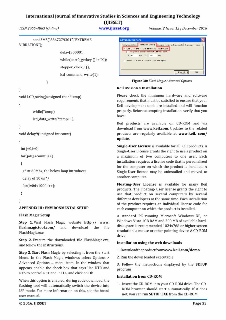
International Journal of Innovative Studies in Sciences and Engineering Technology
(IJISSET)
ISSN 2455-4863 (Online) www.ijisset.org Volume: 2 Issue: 12 | December 2016
© 2016, IJISSET Page 53
sendSMS("8867279301","EXTREME
VIBRATION");
delay(30000);
while(uart0_getkey () != 'K');
stepper_clock_1();
lcd_command_write(1);
}
}
void LCD_string(unsigned char *temp)
{
while(*temp)
lcd_data_write(*temp++);
}
void delay9(unsigned int count)
{
int j=0,i=0;
for(j=0;j<count;j++)
{
/* At 60Mhz, the below loop introduces
delay of 10 us */
for(i=0;i<1000;i++);
}
}
APPENDIX III : ENVIRONMENTAL SETUP
Flash Magic Setup
Step 1. Visit Flash Magic website http:// www.
flashmagictool.com/ and download the file
FlashMagic.exe.
Step 2. Execute the downloaded file FlashMagic.exe,
and follow the instructions.
Step 3. Start Flash Magic by selecting it from the Start
Menu. In the Flash Magic windows select Options >
Advanced Options ... menu item. In the window that
appears enable the check box that says Use DTR and
RTS to control RST and P0.14, and click on Ok.
When this option is enabled, during code download, the
flashing tool will automatically switch the device into
ISP mode. For more information on this, see the board
user manual.
Figure 30: Flash Magic Advanced Options
Keil uVision 4 Installation
Please check the minimum hardware and software
requirements that must be satisfied to ensure that your
Keil development tools are installed and will function
properly. Before attempting installation, verify that you
have:
Keil products are available on CD-ROM and via
download from www.keil.com. Updates to the related
products are regularly available at www.keil. com/
update.
Single-User License is available for all Keil products. A
Single-User License grants the right to use a product on
a maximum of two computers to one user. Each
installation requires a license code that is personalized
for the computer on which the product is installed. A
Single-User license may be uninstalled and moved to
another computer.
Floating-User License is available for many Keil
products. The Floating- User license grants the right to
use that product on several computers by several
different developers at the same time. Each installation
of the product requires an individual license code for
each computer on which the product is installed.
A standard PC running Microsoft Windows XP, or
Windows Vista 1GB RAM and 500 MB of available hard-
disk space is recommended 1024x768 or higher screen
resolution; a mouse or other pointing device A CD-ROM
drive
Installation using the web downloads
1. Downloadtheproductfromwww.keil.com/demo
2. Run the down loaded executable
3. Follow the instructions displayed by the SETUP
program
Installation from CD-ROM
1. Insert the CD-ROM into your CD-ROM drive. The CD-
ROM browser should start automatically. If it does
not, you can run SETUP.EXE from the CD-ROM.

International Journal of Innovative Studies in Sciences and Engineering Technology
(IJISSET)
ISSN 2455-4863 (Online) www.ijisset.org Volume: 2 Issue: 12 | December 2016
© 2016, IJISSET Page 54
2. Select Install Products & Updates from the CD
Browser menu
3. Follow the instructions displayed by the SETUP
program
Procedure for connecting controller pins to the
sensors:
Detailed procedure to connect controller board to the
sensors is as follows:
Table 5: Connections b/w controller and sensors
Input/output Pin no. on controller board
Entry IR sensor P1.16
Exit IR sensor P1.17
First coil of stepper motor P1.4
Second coil of stepper motor P1.5
Third coil of stepper motor P1.6
Fourth coil of stepper motor P1.7
Load sensor P1.12
Vibrator sensor P1.24
Analog to Digital convertor AD0.1
LCD D4 P1.18
LCD D5 P1.19
LCD D6 P1.20
LCD D7 P1.21
LCD RS RS of controller
LCD RW RW of controller
LCD EN EN of controller
Zigbee Tx Rx of controller (UART 0)
Zigbee Rx Tx of controller (UART 0)
GSM Tx Rx of controller (UART 1)
GSM Rx Tx of controller (UART 1)
AUTHOR'S BIOGRAPHY
Mr.Anand Kumar Jha is currently
working as a software engineer at
Manhattan Associates,Bangalore.He
has got overral 2 years of IT
Industry experience (Supply
Chain). He is an alumini of
PESIT,2010-2014th Batch. He has completed his engineering in Electronics &
Communication in 2014 with 8.15 CGPA from PES
INSTUTUTE OF TECHNOLOGY(PESIT),Bangalore.
During this four year tenure,he has done extremely
well both in academics and co-curricular activities.
He has secured top grades(S) for his final year
project(Bridge Monitoring System) and reprented it
at various levels.
Anand has participated in various co-curricular
activities during the year and was also a part of
CORI(Cruscible of Research & Innovation) team(PESIT)
in building small nano satellite during first year of
engineering which got appreciation from ISRO and
about to get launched soon.
He is also an active volunteer of World Vision India and
have sponsored a girl child regarding her education
and overral development.