Embed Size (px)
Citation preview
3.024
“Electronic, Optical, and Magnetic Properties of Materials”
1

• How can we understand and predict electrical, optical and magnetic properties?
Emphasis on fundamental physical models in lectures
• Application to real life situations?
Emphasis on real life examples in HW and recitations
• How do we measure EOM properties?
Emphasis on property measurements in labs using modern state-of-the-art tools
• Can materials properties be engineered?
Property engineering labs
3.024 Objectives and Approach
2
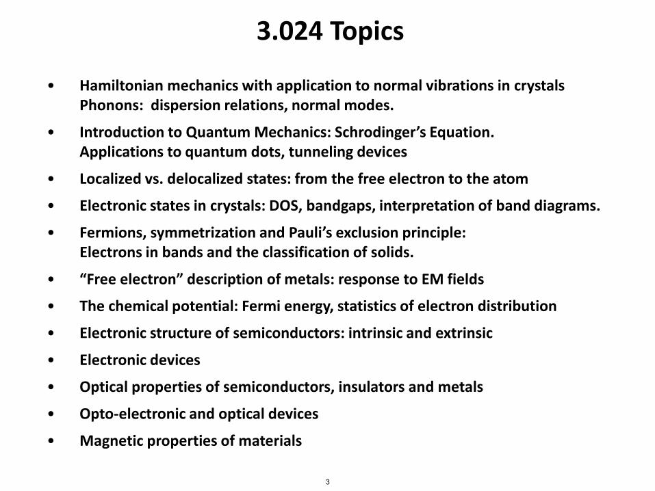
• Hamiltonian mechanics with application to normal vibrations in crystals Phonons: dispersion relations, normal modes.
• Introduction to Quantum Mechanics: Schrodinger’s Equation. Applications to quantum dots, tunneling devices
• Localized vs. delocalized states: from the free electron to the atom
• Electronic states in crystals: DOS, bandgaps, interpretation of band diagrams.
• Fermions, symmetrization and Pauli’s exclusion principle: Electrons in bands and the classification of solids.
• “Free electron” description of metals: response to EM fields
• The chemical potential: Fermi energy, statistics of electron distribution
• Electronic structure of semiconductors: intrinsic and extrinsic
• Electronic devices
• Optical properties of semiconductors, insulators and metals
• Opto-electronic and optical devices
• Magnetic properties of materials
3.024 Topics
3
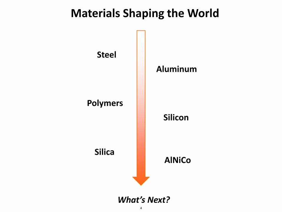
Materials Shaping the World
Steel
Aluminum
Polymers
AlNiCo
Silicon
Silica
What’s Next? 4
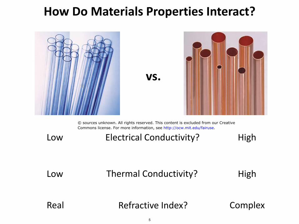
How Do Materials Properties Interact?
vs.
Electrical Conductivity? Low
Real Refractive Index?
High
High
Complex
Low Thermal Conductivity?
© sources unknown. All rights reserved. This content is excluded from our CreativeCommons license. For more information, see http://ocw.mit.edu/fairuse.
5

Materials Under Voltage
I
V R
V
I Rectification, Non-linear, Non-Ohmic
V
I
Linear, Ohmic V=IR
•What determines whether material be a resistor or a diode?
•How would you predict it?
•How much voltage or current can material handle?
•What happens if we shine light onto a material?
light
dark
Steel rods and silicon ingot prior to slicing © sources unknown. This content is excluded fromour Creative Commons license. For more information, see http://ocw.mit.edu/fairuse.
6
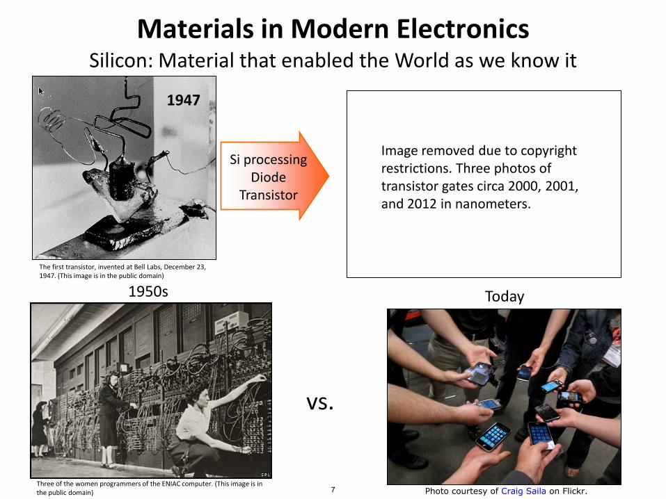
Materials in Modern Electronics Silicon: Material that enabled the World as we know it
Si processing Diode
Transistor
Today
vs.
Image removed due to copyright restrictions. Three photos of transistor gates circa 2000, 2001, and 2012 in nanometers.
1947
The first transistor, invented at Bell Labs, December 23, 1947. (This image is in the public domain)
1950s
Three of the women programmers of the ENIAC computer. (This image is in the public domain) Photo courtesy of Craig Saila on Flickr.7

Does Size Matter?
Could materials properties be size dependent?
Photo courtesy of Kerrythis on Flickr.
8

Size dependent absorption and emission of CdSe nanocrystals (quantum dots)
CdSe is a tetrahedral semiconductor with a Wurtzite structure absorption edge at 1.741eV (@295K):
1. How does it become transparent?
2. Why does it emit light upon excitation?
3. Why does the wavelength of emission depend on the size?
What Happens When Materials Become NANO?
d
“Particle in a box”
Courtesy of Bawendi Lab at MIT. Used with permission.
9Courtesy of Felice Frankel. Used with permission.
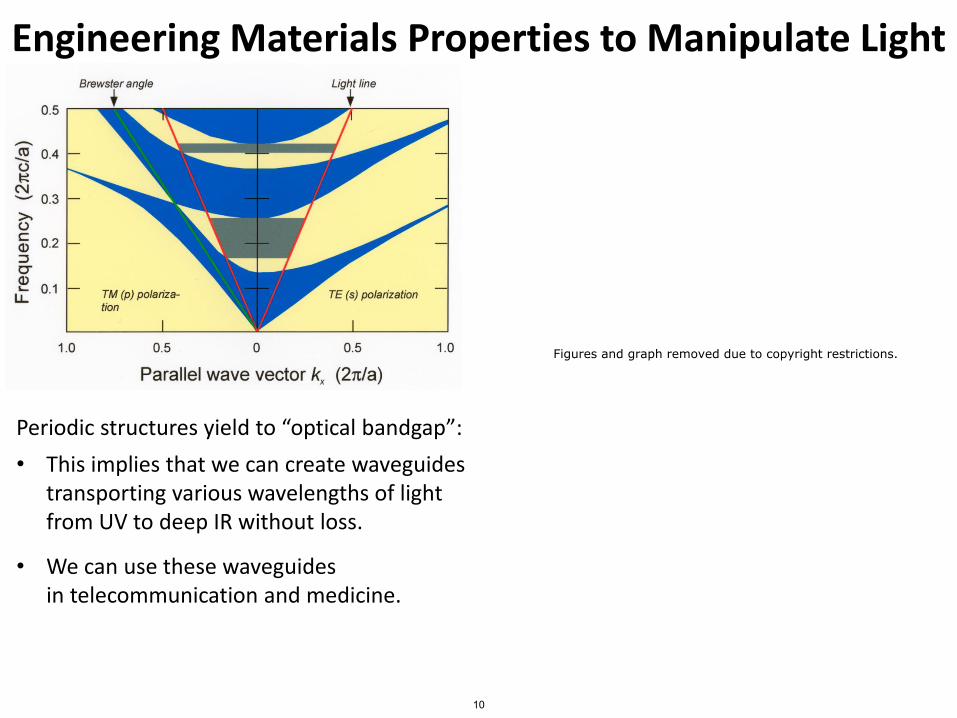
Engineering Materials Properties to Manipulate Light
Periodic structures yield to “optical bandgap”:
• This implies that we can create waveguides transporting various wavelengths of light from UV to deep IR without loss.
• We can use these waveguides in telecommunication and medicine.
Figures and graph removed due to copyright restrictions.
10

Magnets Around Us
Can energy dissipation be useful?
Neurons expressing heat sensitive proteins
Magnetic nanoparticles converting EM waves to heat
Use magnetic nanoantennae to stimulate neurons: Non-invasive treatments of neuro-disorders
Anikeeva Lab @ DMSE
From Prof. Beach
. From Prof Beach
© R. Nave. All rights reserved. This content is excluded from our Creative Commonslicense. For more information, see http://ocw.mit.edu/fairuse.
11

MIT OpenCourseWarehttp://ocw.mit.edu
3.024 Electronic, Optical and Magnetic Properties of MaterialsSpring 2013
For information about citing these materials or our Terms of Use, visit: http://ocw.mit.edu/terms.

![Application of differential effective medium, magnetic ... · [1] A differential effective medium (DEM) model is used to predict elastic properties for a set of porous and anisotropic](https://img.pdfslide.net/doc/110x75/5fbef87136a77a10ff711f01/application-of-differential-effective-medium-magnetic-1-a-differential-effective.jpg)