Embed Size (px)
Citation preview
USER’S MANUAL
AN1881Rev 1.00
September 25, 2013
ISL8115EVAL1ZSynchronous Buck Converter
IntroductionThe ISL8115EVAL1Z is a Synchronous Buck Converter implementing Intersil’s wide input range PWM controller ISL8115. Utilizing voltage mode control with input feed-forward, the ISL8115EVAL1Z maintains a constant loop gain for optimal transient response, especially for applications with a wide input voltage range. For a more detailed description of the ISL8115 functionality, refer to the ISL8115 data sheet.
This application note includes the test setup, typical performance waveforms, schematic, layout and Bill of Materials (BOM).
Evaluation Board Specifications
ISL8115 Key Features• Wide VIN range operation: 2.97V to 36V; up to 5.5V output
and 30A load current per phase.
• Fast transient response
- Voltage-mode PWM leading-edge modulation with non-linear control
- Input voltage feed-forward
• Integrated 5V high speed 4A MOSFET gate drivers
- Internal bootstrap diode
• Oscillator programmable from 150kHz to 1.5MHz
- Frequency synchronization to external clock signal
• Diode emulation mode for light load efficiency improvement
• Output OVP/UVP; OCP and OTP
• Power-good open drain output
• Adjustable soft-start
• Pre-bias start-up function
• Excellent output voltage regulation
- 0.6V ±1.0% internal reference (-40°C~125°C)
- 0.6V ±0.7% internal reference (-40°C~105°C)
- Differential voltage sensing
Applications• Power supply for datacom/telecom and POL
• Wide input voltage range buck regulators
• High current density power supplies RF power amplifier bias compensation
Recommended Equipment• Input power source up to 15V supply voltage with 60W
power supply ability
• Electronic load with 50W power sinking ability
• Voltmeters and ammeters
• 100MHz quad-trace oscilloscope
TABLE 1. EVALUATION BOARD ELECTRICAL SPECIFICATIONS
SPEC DESCRIPTION MIN TYP MAX UNIT
VIN Board Input Range 10 12 15 V
VOUT Output Voltage 1.5 V
IOUT Output Rated Current 30 A
IOC Overcurrent Threshold 32 A
Fsw Switch Frequency 220 kHz
Input UVP Rising threshold 9.7 V
Falling threshold 9.2 V
η Efficiency at 50% load 90.88 %
FIGURE 1. ISL8115EVAL1Z EVALUATION BOARD
AN1881 Rev 1.00 Page 1 of 12September 25, 2013
ISL8115EVAL1Z
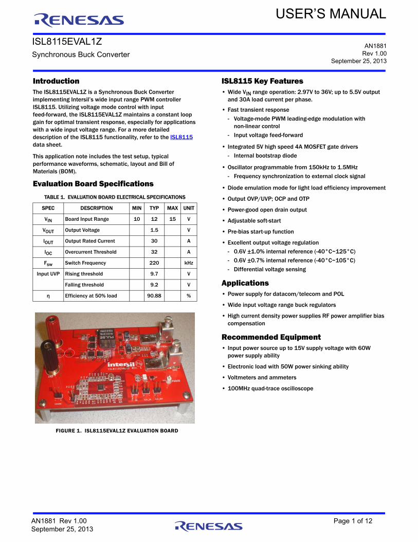
Quick Test Setup1. Ensure that the Evaluation board is correctly connected to the
power supply and the electronic load prior to applying any power. Please refer to Figure 2 for proper set-up.
2. Set the input voltage to 12V, turn on the power supply and observe output voltage. The output voltage should variation should be within 5%.
3. Adjust load current within 30A. The output voltage variation should be within 5%.
4. Use oscilloscope to observe output ripple voltage and phase node ringing. For accurate measurement, please refer to Figure 3 for proper set-up.
Note: Test points TP1; TP3; TP8; TP9 are for voltage measurement only. Do not allow high current through these test points.
Probe Set-up
Design GuideThe ISL8115EVAL1Z is optimized for 10V to 15V input voltage range. However, the evaluation board can be modified to support multiple applications due to the customer requirements. Please refer to the datasheet for the detailed information.
Output Voltage AdjustmentThe output voltage can be set by the resistor R4, R1. In order to keep the existing compensation parameters unchanged, adjust R4 to set the output voltage by the following Equation 1:
VMON monitors the output for UVP and OVP, the resistor divider value of R11/R8 should be the same with the R1/R4.
Synchronization ISL8115EVAL1Z board can be synchronized with an external clock. Apply a clock signal (10% to 90% duty cycle) in the range of 150kHz to 1.5MHz to the FSET pin makes the internal frequency synchronized with the external clock. Please remove R27 when the sync function is implemented.
FIGURE 2. ISL8115EVAL1Z TEST SET-UP
FIGURE 3. OSCILLOSCOPE PROBE SET-UP
V6.0Vout
1RV6.04R
(EQ. 1)
AN1881 Rev 1.00 Page 2 of 12September 25, 2013
ISL8115EVAL1Z
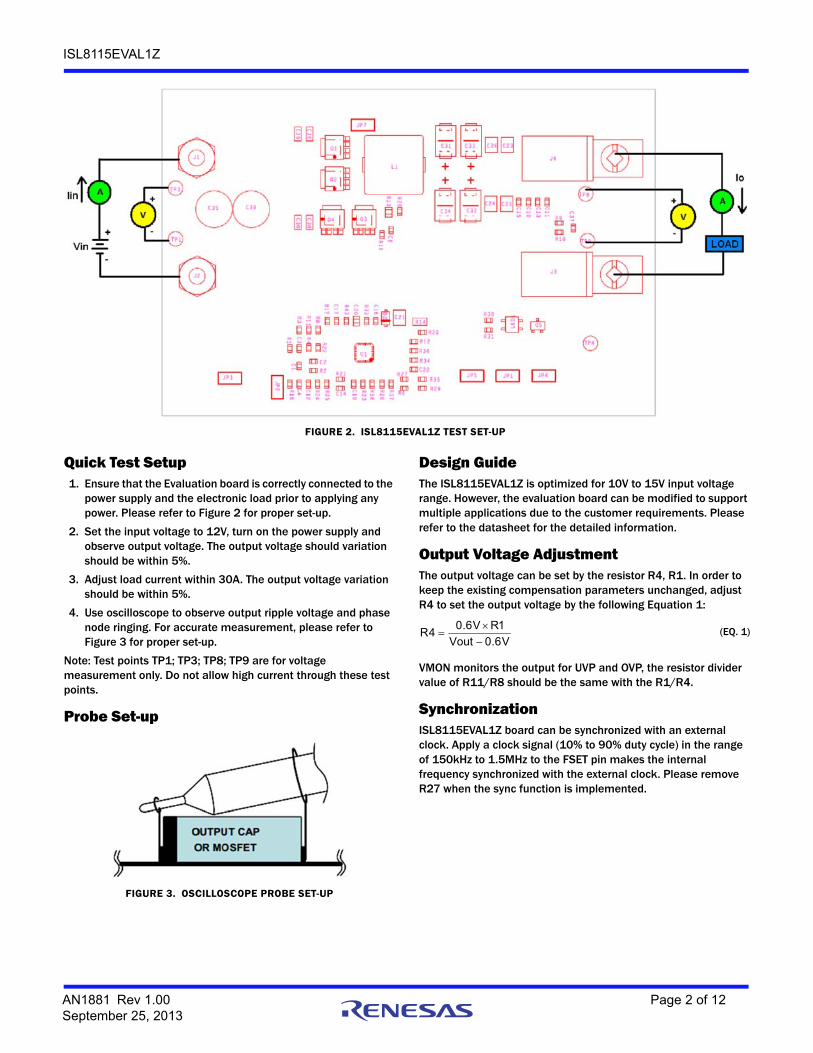
Typical Performance Curves Unless otherwise specified, the input voltage is 12V.
FIGURE 4. EFFICIENCY vs LOAD CURRENT AT CCM MODE FIGURE 5. EFFICIENCY vs LOAD CURRENT AT DEM MODE
FIGURE 6. VOUT LOAD REGULATION AT CCM MODE FIGURE 7. VOUT LOAD REGULATION AT DEM MODE
FIGURE 8. LINE REGULATION AT NO LOAD CONDITION
6062646668707274767880828486889092
0 5 10 15 20 25 30
OUTPUT CURRENT (A)
EF
FIC
IEN
CY
(%
)
VIN = 10.5V
VIN = 12V
VIN = 13.5V
6062646668707274767880828486889092
0 2 4 6 8 10
OUTPUT CURRENT (A)
EF
FIC
IEN
CY
(%
)
VIN = 10.5V
VIN = 12V
VIN = 13.5V
1.5019
1.5020
1.5021
1.5022
1.5023
1.5024
1.5025
1.5026
1.5027
1.5028
1.5029
0 2 4 6 8 10 12 14 16 18 20 22 24 26 28 30
VIN = 12V
LOAD CURRENT (A)
VO
UT (
V)
1.5020
1.5021
1.5022
1.5023
1.5024
1.5025
1.5026
1.5027
1.5028
1.5029
0 2 4 6 8 10 12 14 16 18 20 22 24 26 28 30
LOAD CURRENT (A)
VO
UT (
V)
VIN = 12V
1.5018
1.5021
1.5024
1.5027
1.5030
10.5 11.0 11.5 12.0 12.5 13.0 13.5
NO LOAD
VIN (V)
CCM MODE
VO
UT (
V)
1.5018
1.5021
1.5024
1.5027
1.5030
1.5033
1.5036
10.5 11.0 11.5 12.0 12.5 13.0 13.5
NO LOAD
VIN (V)
DEM MODE
VO
UT (
V)
AN1881 Rev 1.00 Page 3 of 12September 25, 2013
ISL8115EVAL1Z
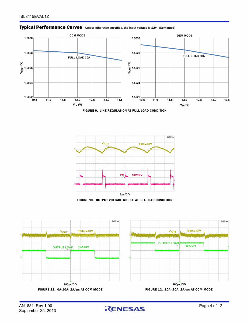
FIGURE 9. LINE REGULATION AT FULL LOAD CONDITION
FIGURE 10. OUTPUT VOLTAGE RIPPLE AT 30A LOAD CONDITION
FIGURE 11. 0A-10A; 2A/µs AT CCM MODE FIGURE 12. 10A -20A; 2A/µs AT CCM MODE
Typical Performance Curves Unless otherwise specified, the input voltage is 12V. (Continued)
1.5022
1.5024
1.5026
1.5028
1.5030
10.5 11.0 11.5 12.0 12.5 13.0 13.5
FULL LOAD 30A
VIN (V)
CCM MODE
VO
UT (
V)
1.5022
1.5024
1.5026
1.5028
1.5030
10.5 11.0 11.5 12.0 12.5 13.0 13.5
FULL LOAD 30A
VIN (V)
DEM MODE
VO
UT (
V)
VOUT
2µs/DIV
PH
50mV/DIV
10V/DIV
OUTPUT LOAD
200µs/DIV
VOUT 100mV/DIV
10A/DIV
200µs/DIV
VOUT
OUTPUT LOAD
100mV/DIV
10A/DIV
AN1881 Rev 1.00 Page 4 of 12September 25, 2013
ISL8115EVAL1Z
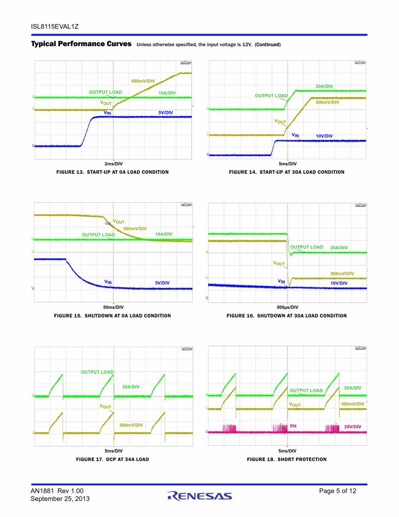
FIGURE 13. START-UP AT 0A LOAD CONDITION FIGURE 14. START-UP AT 30A LOAD CONDITION
FIGURE 15. SHUTDOWN AT 0A LOAD CONDITION FIGURE 16. SHUTDOWN AT 30A LOAD CONDITION
FIGURE 17. OCP AT 34A LOAD FIGURE 18. SHORT PROTECTION
Typical Performance Curves Unless otherwise specified, the input voltage is 12V. (Continued)
VOUT
OUTPUT LOAD
2ms/DIV
VIN
500mV/DIV
10A/DIV
5V/DIV
5ms/DIV
VOUT
OUTPUT LOAD
VIN
500mV/DIV
20A/DIV
10V/DIV
50ms/DIV
VOUT
OUTPUT LOAD
VIN
500mV/DIV10A/DIV
5V/DIV
500µs/DIV
VOUT
OUTPUT LOAD
VIN
500mV/DIV
20A/DIV
10V/DIV
VOUT
OUTPUT LOAD
5ms/DIV
500mV/DIV
20A/DIV
VOUT
PH
OUTPUT LOAD
5ms/DIV
500mV/DIV
20A/DIV
20V/DIV
AN1881 Rev 1.00 Page 5 of 12September 25, 2013
AN
18
81R
ev 1.0
0P
age 6 of 1
2S
eptem
ber 2
5, 201
3
ISL8
115
EV
AL1
Z
TP3PVIN
C24100uF
J4
Big Lug
1
C34DNP C31
DNP
C33
6TPF330M9L
C26100uF
C101uF
J3
Big Lug
1
C111uF
C25100uF
C326TPF330M9L
C131uF
C151uF
J1VIN
VOUT
12VTP1
GND J2GND
PC39DNP
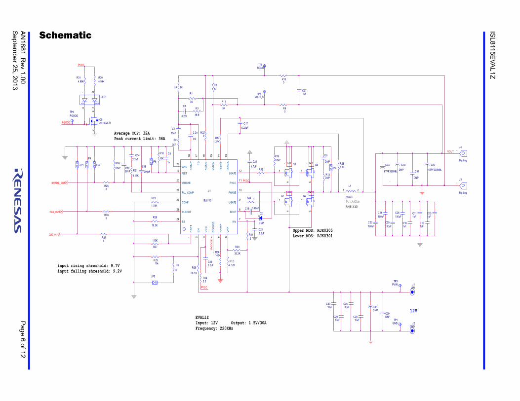
Schematic
Q431 2
4
5
C23100uF
U1
ISL8115IRTZ
ISET19
ISHARE20
RG
ND
16
RA
MP
5
PLL_COMP21
VIN7
CONF22
SS24
CLKOUT23
FB
17
VC
C3
EN
2
ISE
NB
14
VM
ON
15
FS
ET
1
PG
OO
D4
VF
F6
UGATE9
PHASE10
PVCC11
LGATE12IS
EN
A13
BOOT8
CO
MP
18
GND25
C212.2uFR14
2
R20
33.2K
Q1
31 2
4
5
Q331 2
4
5
L1
320nH
PA1513.321
21
R124.12K
C16 0.22uF
C204.7uF
Upper MOS: RJK0305Lower MOS: RJK0301
R36140K
C222.2uF
R35
68.1K
R27
113K
R26
18.2K
R23
11.8K
C133nF
R2787
R4 2K
C19
390pFR21
5.11K
C142.2nF
R18
10KC4
1n R282.8K
C170.22uF
R171.27K
R11
3K
R82K
C3
8.2nF
R3
49.9
R1
3K
C2
2.2n
R2910k
R342.2
PVCC
TP8VOUT_S
TP9RGND
JP5
R90
R100
C371uF
R610
R380
CLK_OUT
R370
CLK_IN
ISHARE_BUSR250
PVCC
RED GREEN
LED1
12
34
R304.99K
TP4PGOOD
Q52N7002LT1
3
1
2
R314.99K
PGOOD
EVAL1ZInput: 12V Output: 1.5V/30A Frequency: 220KHz
input rising shreshold: 9.7Vinput falling shreshold: 9.2V
Average OCP: 32APeak current limit: 36A
JP6
C12DNP
R24DNP
JP3JP1
JP4
D2
DNP
PVCC
0.53mOhm
R13DNP
C6
DNP
JP7
R220
PG
OO
D
Q2
31 2
4
5
R33 0
R43
0
R16DNP
C35DN
C3010uF
C2910uF
C3610uF
C3810uF
ISL8115EVAL1Z
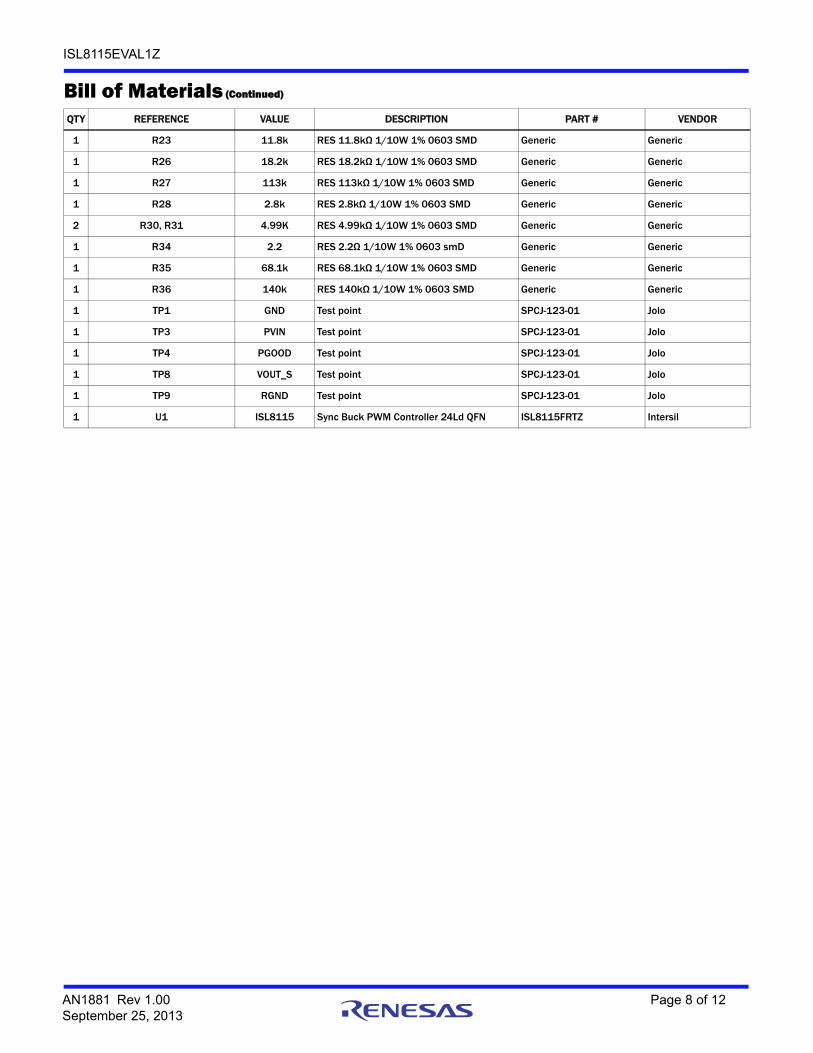
Bill of MaterialsQTY REFERENCE VALUE DESCRIPTION PART # VENDOR
1 C1 33nF CAP CER 0.033µF 50V 10% X7R 0603 Generic Generic
1 C2 2.2n CAP CER 2200pF 50V 5% NP0 0603 Generic Generic
1 C3 8.2n CAP CER 8200pF 50V 5% NP0 0603 Generic Generic
1 C4 1n CAP CER 1000pF 50V 5% NP0 0603 Generic Generic
5 C6, C12, R13, R16, R24 DNP Generic Generic
5 C10, C11, C13, C15, C37 1µF CAP CER 1µF 10V 10% X5R 0603 Generic Generic
1 C14 2.2nF CAP CER 2200pF 50V 5% NP0 0603 Generic Generic
2 C16, C17 0.22µF CAP CER 0.22µF 16V 10% X7R 0603 Generic Generic
1 C19 390pF CAP CER 390pF 50V 5% NP0 0603 Generic Generic
1 C20 4.7µF CAP CER 4.7µF 6.3V 10% X5R 0805 Generic Generic
1 C21 2.2µF CAP CER 2.2µF 25V 10% X7R 1210 C3225X7R1E225K/1.60 TDK
1 C22 2.2µF CAP CER 2.2µF 6.3V 20% X5R 0603 Generic Generic
4 C23, C24, C25, C26 100µF CAP CER 100µF 6.3V 20% X5R 1210 C3225X5R0J107M250AC TDK
4 C29, C30, C36, C38 10µF CAP CER 10µF 50V 10% X5R 1206 C3216X5R1H106K160AB TDK
2 C31, C34 DNP CAP TANT 330µF 6.3V 20% 2917 6TPF330M9L Panasonic
2 C32, C33 6TPF330M9L CAP TANT 330µF 6.3V 20% 2917 6TPF330M9L Panasonic
2 C35, C39 DNP CAP OS-CON 270µF 16V 16SEPC270MX Panasonic
1 D2 DNP DIODE SCHOTTKY 40V SOD123
6 JP1, JP3, JP4, JP5, JP6, JP7 Jumper JUMPER PLUG 2POS DOUBLE ROW XG8T-0231 Omron
1 J1 VIN POST BINDING BANANA INSULATED RE 111-0707-001 Johnson Components
1 J2 GND POST BINDING BANANA INSULATED BL 111-0703-001 Johnson Components
2 J3, J4 Big Lug CONN- Big Lug TERMINAL POST KPA8CTP Burndy
1 LED1 LXA3025IGC-TR LED LNJ162C3XRA Panasonic
1 L1 320nH INDUCT PWR 320NH SMD PA1513.321 Pulse
2 Q1, Q2 RJK0305 MOSFET N-CH 30V 30A 5-LFPAK RJK0305DPB-00#J0 Renesas
2 Q3, Q4 RJK0328 MOSFET N-CH 30V 30A 5-LFPAK RJK0305DPB-00#J0 Renesas
1 Q5 2N7002LT1 MOSFET N-CH 60V 115mA SOT-23 2N7002LT1 ON Semiconductor
2 R1, R11 3k RES 3.00kΩ 1/10W 1% 0603 SMD Generic Generic
1 R2 787 RES 787Ω 1/10W 1% 0603 SMD Generic Generic
1 R3 49.9 RES 49.9Ω 1/10W 1% 0603 SMD Generic Generic
2 R4, R8 2k RES 2.00kΩ 1/10W 1% 0603 SMD Generic Generic
1 R6 10 RES 10Ω 1/10W 1% 0603 SMD Generic Generic
8 R9, R10, R22, R25, R33, R37, R38, R43
0 RES 0.0Ω 1/10W JUMP 0603 SMD Generic Generic
1 R12 4.12k RES 4.12kΩ 1/10W 1% 0603 SMD Generic Generic
1 R14 2 RES 2.00Ω 1/4W 1% 1206 SMD Generic Generic
1 R17 1.27k RES 1.27kΩ 1/10W 1% 0603 SMD Generic Generic
2 R18, R29 10k RES 10kΩ 1/10W 1% 0603 SMD Generic Generic
1 R20 33.2k RES 33.2kΩ 1/10W 1% 0603 SMD Generic Generic
1 R21 5.11k RES 5.11kΩ 1/10W 1% 0603 SMD Generic Generic
AN1881 Rev 1.00 Page 7 of 12September 25, 2013
ISL8115EVAL1Z
1 R23 11.8k RES 11.8kΩ 1/10W 1% 0603 SMD Generic Generic
1 R26 18.2k RES 18.2kΩ 1/10W 1% 0603 SMD Generic Generic
1 R27 113k RES 113kΩ 1/10W 1% 0603 SMD Generic Generic
1 R28 2.8k RES 2.8kΩ 1/10W 1% 0603 SMD Generic Generic
2 R30, R31 4.99K RES 4.99kΩ 1/10W 1% 0603 SMD Generic Generic
1 R34 2.2 RES 2.2Ω 1/10W 1% 0603 smD Generic Generic
1 R35 68.1k RES 68.1kΩ 1/10W 1% 0603 SMD Generic Generic
1 R36 140k RES 140kΩ 1/10W 1% 0603 SMD Generic Generic
1 TP1 GND Test point SPCJ-123-01 Jolo
1 TP3 PVIN Test point SPCJ-123-01 Jolo
1 TP4 PGOOD Test point SPCJ-123-01 Jolo
1 TP8 VOUT_S Test point SPCJ-123-01 Jolo
1 TP9 RGND Test point SPCJ-123-01 Jolo
1 U1 ISL8115 Sync Buck PWM Controller 24Ld QFN ISL8115FRTZ Intersil
Bill of Materials (Continued)
QTY REFERENCE VALUE DESCRIPTION PART # VENDOR
AN1881 Rev 1.00 Page 8 of 12September 25, 2013
AN
18
81R
ev 1.0
0P
age 9 of 1
2S
eptem
ber 2
5, 201
3
ISL8
115
EV
AL1
Z
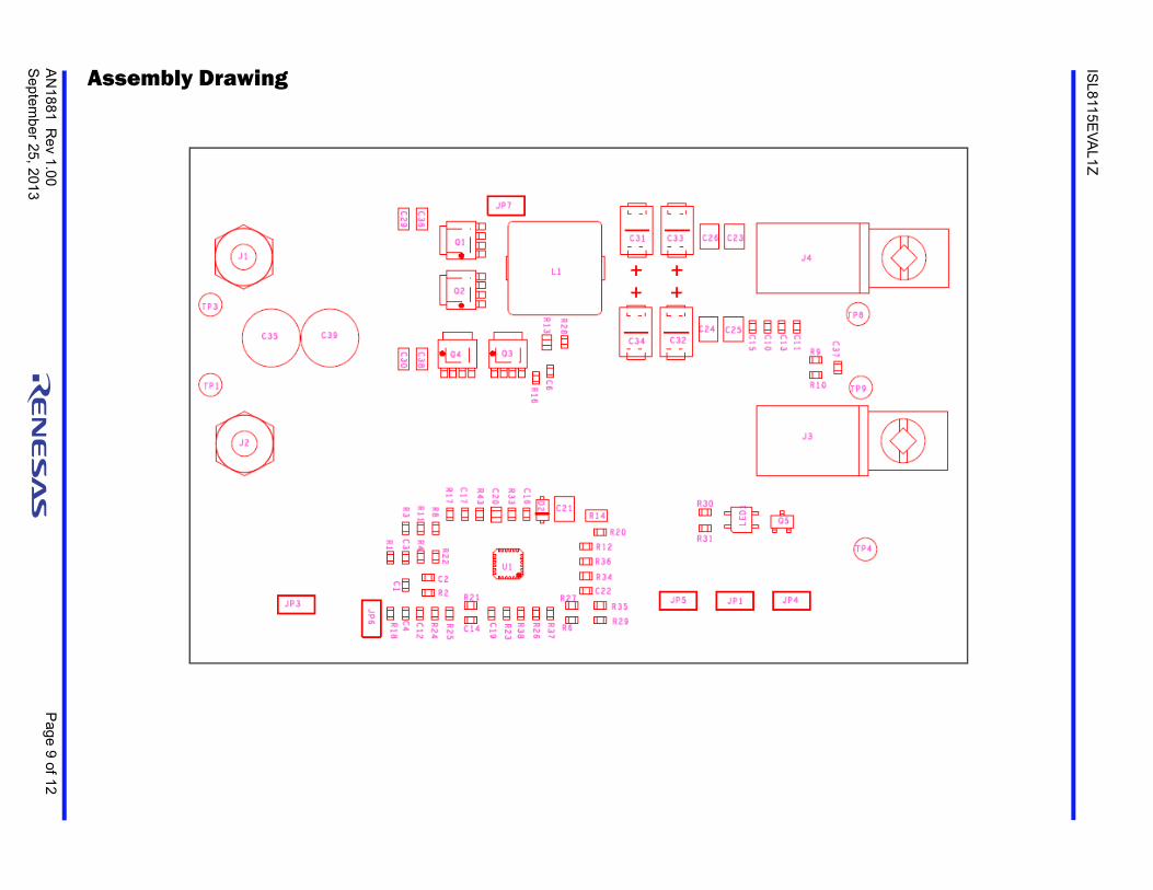
Assembly Drawing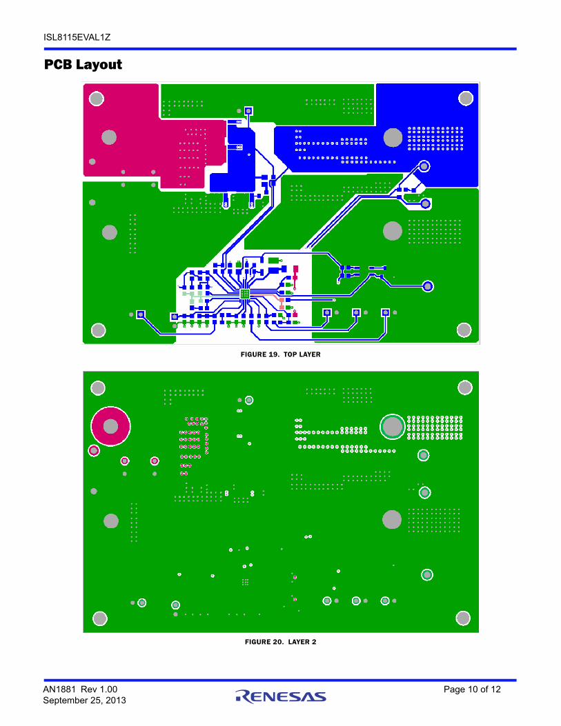
ISL8115EVAL1Z
PCB Layout
FIGURE 19. TOP LAYER
FIGURE 20. LAYER 2
AN1881 Rev 1.00 Page 10 of 12September 25, 2013
ISL8115EVAL1Z
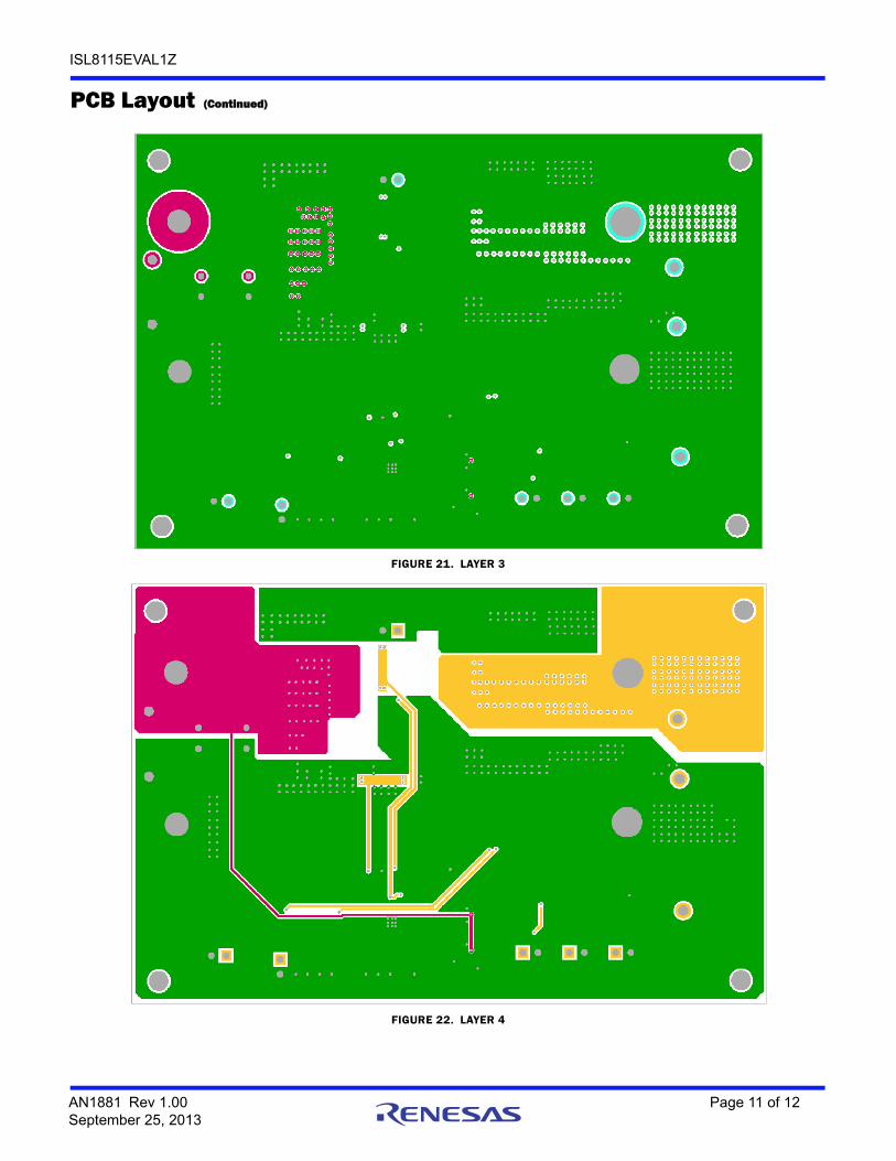
FIGURE 21. LAYER 3
FIGURE 22. LAYER 4
PCB Layout (Continued)
AN1881 Rev 1.00 Page 11 of 12September 25, 2013
http://www.renesas.comRefer to "http://www.renesas.com/" for the latest and detailed information.
Renesas Electronics America Inc.1001 Murphy Ranch Road, Milpitas, CA 95035, U.S.A.Tel: +1-408-432-8888, Fax: +1-408-434-5351Renesas Electronics Canada Limited9251 Yonge Street, Suite 8309 Richmond Hill, Ontario Canada L4C 9T3Tel: +1-905-237-2004Renesas Electronics Europe LimitedDukes Meadow, Millboard Road, Bourne End, Buckinghamshire, SL8 5FH, U.KTel: +44-1628-651-700, Fax: +44-1628-651-804Renesas Electronics Europe GmbHArcadiastrasse 10, 40472 Düsseldorf, Germany Tel: +49-211-6503-0, Fax: +49-211-6503-1327Renesas Electronics (China) Co., Ltd.Room 1709 Quantum Plaza, No.27 ZhichunLu, Haidian District, Beijing, 100191 P. R. ChinaTel: +86-10-8235-1155, Fax: +86-10-8235-7679Renesas Electronics (Shanghai) Co., Ltd.Unit 301, Tower A, Central Towers, 555 Langao Road, Putuo District, Shanghai, 200333 P. R. China Tel: +86-21-2226-0888, Fax: +86-21-2226-0999Renesas Electronics Hong Kong LimitedUnit 1601-1611, 16/F., Tower 2, Grand Century Place, 193 Prince Edward Road West, Mongkok, Kowloon, Hong KongTel: +852-2265-6688, Fax: +852 2886-9022Renesas Electronics Taiwan Co., Ltd.13F, No. 363, Fu Shing North Road, Taipei 10543, TaiwanTel: +886-2-8175-9600, Fax: +886 2-8175-9670Renesas Electronics Singapore Pte. Ltd.80 Bendemeer Road, Unit #06-02 Hyflux Innovation Centre, Singapore 339949Tel: +65-6213-0200, Fax: +65-6213-0300Renesas Electronics Malaysia Sdn.Bhd.Unit 1207, Block B, Menara Amcorp, Amcorp Trade Centre, No. 18, Jln Persiaran Barat, 46050 Petaling Jaya, Selangor Darul Ehsan, MalaysiaTel: +60-3-7955-9390, Fax: +60-3-7955-9510Renesas Electronics India Pvt. Ltd.No.777C, 100 Feet Road, HAL 2nd Stage, Indiranagar, Bangalore 560 038, IndiaTel: +91-80-67208700, Fax: +91-80-67208777Renesas Electronics Korea Co., Ltd.17F, KAMCO Yangjae Tower, 262, Gangnam-daero, Gangnam-gu, Seoul, 06265 KoreaTel: +82-2-558-3737, Fax: +82-2-558-5338
SALES OFFICES
© 2018 Renesas Electronics Corporation. All rights reserved.Colophon 7.0
(Rev.4.0-1 November 2017)
Notice
1. Descriptions of circuits, software and other related information in this document are provided only to illustrate the operation of semiconductor products and application examples. You are fully responsible for
the incorporation or any other use of the circuits, software, and information in the design of your product or system. Renesas Electronics disclaims any and all liability for any losses and damages incurred by
you or third parties arising from the use of these circuits, software, or information.
2. Renesas Electronics hereby expressly disclaims any warranties against and liability for infringement or any other claims involving patents, copyrights, or other intellectual property rights of third parties, by or
arising from the use of Renesas Electronics products or technical information described in this document, including but not limited to, the product data, drawings, charts, programs, algorithms, and application
examples.
3. No license, express, implied or otherwise, is granted hereby under any patents, copyrights or other intellectual property rights of Renesas Electronics or others.
4. You shall not alter, modify, copy, or reverse engineer any Renesas Electronics product, whether in whole or in part. Renesas Electronics disclaims any and all liability for any losses or damages incurred by
you or third parties arising from such alteration, modification, copying or reverse engineering.
5. Renesas Electronics products are classified according to the following two quality grades: “Standard” and “High Quality”. The intended applications for each Renesas Electronics product depends on the
product’s quality grade, as indicated below.
"Standard": Computers; office equipment; communications equipment; test and measurement equipment; audio and visual equipment; home electronic appliances; machine tools; personal electronic
equipment; industrial robots; etc.
"High Quality": Transportation equipment (automobiles, trains, ships, etc.); traffic control (traffic lights); large-scale communication equipment; key financial terminal systems; safety control equipment; etc.
Unless expressly designated as a high reliability product or a product for harsh environments in a Renesas Electronics data sheet or other Renesas Electronics document, Renesas Electronics products are
not intended or authorized for use in products or systems that may pose a direct threat to human life or bodily injury (artificial life support devices or systems; surgical implantations; etc.), or may cause
serious property damage (space system; undersea repeaters; nuclear power control systems; aircraft control systems; key plant systems; military equipment; etc.). Renesas Electronics disclaims any and all
liability for any damages or losses incurred by you or any third parties arising from the use of any Renesas Electronics product that is inconsistent with any Renesas Electronics data sheet, user’s manual or
other Renesas Electronics document.
6. When using Renesas Electronics products, refer to the latest product information (data sheets, user’s manuals, application notes, “General Notes for Handling and Using Semiconductor Devices” in the
reliability handbook, etc.), and ensure that usage conditions are within the ranges specified by Renesas Electronics with respect to maximum ratings, operating power supply voltage range, heat dissipation
characteristics, installation, etc. Renesas Electronics disclaims any and all liability for any malfunctions, failure or accident arising out of the use of Renesas Electronics products outside of such specified
ranges.
7. Although Renesas Electronics endeavors to improve the quality and reliability of Renesas Electronics products, semiconductor products have specific characteristics, such as the occurrence of failure at a
certain rate and malfunctions under certain use conditions. Unless designated as a high reliability product or a product for harsh environments in a Renesas Electronics data sheet or other Renesas
Electronics document, Renesas Electronics products are not subject to radiation resistance design. You are responsible for implementing safety measures to guard against the possibility of bodily injury, injury
or damage caused by fire, and/or danger to the public in the event of a failure or malfunction of Renesas Electronics products, such as safety design for hardware and software, including but not limited to
redundancy, fire control and malfunction prevention, appropriate treatment for aging degradation or any other appropriate measures. Because the evaluation of microcomputer software alone is very difficult
and impractical, you are responsible for evaluating the safety of the final products or systems manufactured by you.
8. Please contact a Renesas Electronics sales office for details as to environmental matters such as the environmental compatibility of each Renesas Electronics product. You are responsible for carefully and
sufficiently investigating applicable laws and regulations that regulate the inclusion or use of controlled substances, including without limitation, the EU RoHS Directive, and using Renesas Electronics
products in compliance with all these applicable laws and regulations. Renesas Electronics disclaims any and all liability for damages or losses occurring as a result of your noncompliance with applicable
laws and regulations.
9. Renesas Electronics products and technologies shall not be used for or incorporated into any products or systems whose manufacture, use, or sale is prohibited under any applicable domestic or foreign laws
or regulations. You shall comply with any applicable export control laws and regulations promulgated and administered by the governments of any countries asserting jurisdiction over the parties or
transactions.
10. It is the responsibility of the buyer or distributor of Renesas Electronics products, or any other party who distributes, disposes of, or otherwise sells or transfers the product to a third party, to notify such third
party in advance of the contents and conditions set forth in this document.
11. This document shall not be reprinted, reproduced or duplicated in any form, in whole or in part, without prior written consent of Renesas Electronics.
12. Please contact a Renesas Electronics sales office if you have any questions regarding the information contained in this document or Renesas Electronics products.
(Note 1) “Renesas Electronics” as used in this document means Renesas Electronics Corporation and also includes its directly or indirectly controlled subsidiaries.
(Note 2) “Renesas Electronics product(s)” means any product developed or manufactured by or for Renesas Electronics.