Embed Size (px)
Citation preview

Introduction of Power Management IC
Winson Wei,
RDI Division
Product Development Center
Richtek
Oct. 21, 2008

Outline About Richtek and Analog IC Market
Elements of Power Management IC Technology
Field Applications
Power Electronic Technology
Power Management IC Fabrication Technology
Power Management IC Design
Product Development Flow
Summary
Power Management IC Design Contest
CONFIDENTIAL
3
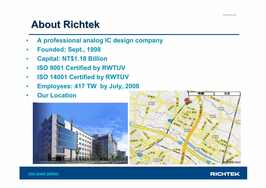
About RichtekAbout Richtek
• A professional analog IC design company
• Founded: Sept., 1998
• Capital: NT$1.18 Billion
• ISO 9001 Certified by RWTUV
• ISO 14001 Certified by RWTUV
• Employees: 417 TW by July, 2008
• Our Location
CONFIDENTIAL
4
Worldwide Branch Office and Distributors
• Headquarters Hsinchu, Taiwan
• Branch office Taipei, Taiwan
Shenzhen, China
Shanghai, China
Beijing, China
Bundang, Korea
Silicon Valley, US
Tokyo, Japan
The Netherlands, Europe
• Distributors Taiwan
China
Japan
USA
Europe
Singapore

CONFIDENTIAL
5
Product Applications
Consumer
Computer
Communication

CONFIDENTIAL
6
Richtek Business Achievement Richtek Business Achievement
0
1,000
2,000
3,000
4,000
5,000
6,000
7,000
Net Sales (NT$M) 350 670 1,104 2,011 2,242 2,684 4,296 6,062
2000 2001 2002 2003 2004 2005 2006 2007

CONFIDENTIAL
7
Worldwide Analog IC Company
(US$m)

CONFIDENTIAL
8
Richtek Product Mix and Share in PMIC Market

CONFIDENTIAL
9
Taiwan Companies’ Share

CONFIDENTIAL
10
By More precise definition of TAM

CONFIDENTIAL
11
Photograph of iBookPro Motherboard -- I

CONFIDENTIAL
12
Photograph of iBookPro Motherboard -- II
CONFIDENTIAL
13
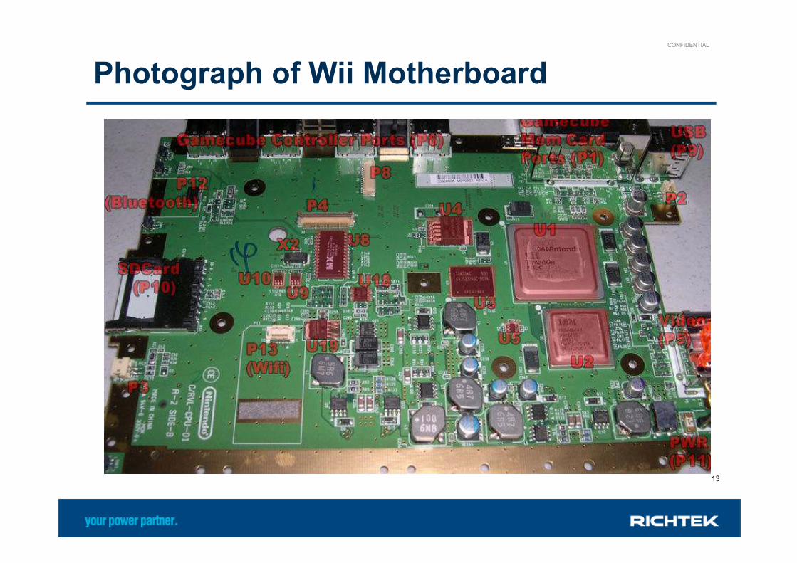
Photograph of Wii Motherboard

CONFIDENTIAL
14
Photograph of MB PCB Zoom-In

CONFIDENTIAL
15
Photograph of VGA Card

CONFIDENTIAL
16
Elements of Power Management IC Technology
Semiconductor
IC Fabrication
Power Electronic
Technology
Analog
Integrated
Circuit
Field
Applications

CONFIDENTIAL
17
Power IC Driving Force -- Applications
DDRXDDRIII 1.2V
DDRII 1.8V
DDRI 2.5V
RMRAMSDRAM 3.3V
EDRAM 3.3V
DRAM DRAM
45nm65nm90nm0.13um0.18um0.25um0.35um0.5um1um
Dual Core 1V
Core 2 Duo 1.2V
Pentium E
1.3V
Pentium 4
1.3V
Pentium III
1.8V
Pentium II
2.5V
Pentium 3V
80486 3.3V
80386 5V
Technology driving
Application driving

CONFIDENTIAL
18
System Block Diagram for DSC
• Battery Management
• DC/DC Converters
• Motor Drivers
• Audio Amplifier
• Backlight Drivers

CONFIDENTIAL
19
Power Requirement for DSC system
• System-On-Chip• VCORE : 1.0/1.2/1.5/1.8V @ 300mA~600mA
• VIO : 2.5/3.3V @ 300mA
• Memory• SDRAM, DDR and Flash: 1.8/2.5/3.3V @ 150mA
• Analog/RF• OSC, PLL, ADC, DAC, RF (LNA/PA), Mic, Headphone and Speaker: 1.3V~3.6V
• Sensors• CCD: VCCD+ = 15~16V @ 50mA and VCCD- = -7~-8V @ 50mA
• CMOS: Dual, 1.8/2.5/3.3V @ 300mA
• Actuators• Motor: 3.3/4.3/5V @ 250mA
• Vibrator: 2.5/3.3V @ 200mA~500mA
• Headphone/Speaker: 100mW~2W.
• LCD Display• LCD Driver SOC: 3.3V @ 100mA
• WLED Backlight: WLED x1/x2/x3/x4/x5/x6 @ 20mA
• Flash Light: WLED x1/x3 @ 100mA~500mA, Xenon Flash @ 300V

CONFIDENTIAL
20
System Block Diagram for TFT LCD
SDRAM
RGBInput
Key
Pad
Scaler
PLL
ADC
OSD
DecoderTMDS
MCU
DVIInput
VideoInput
EEPROM
MB Power
Adaptor
InputT-Con
Gate Driver
Source Driver
Panel Power Inverter
CCFL
TFT Glass

CONFIDENTIAL
21
Block Diagram for TFT LCD Panel
T-Con TFT Panel
Gate Driver
Source Driver
CCFL/LED
Vsource
Inverter/
LED Drivers
2 Level : VGH, VGL
3 Level : VGH, VGL, VGC
Vcom
γγγγ Buffer

CONFIDENTIAL
22
Power Requirement for TFT LCD Panel
• Input Supply Range: 2.6V~6V
• Current Mode BOOST Converter for AVDD• 1.2MHz switching frequency
• Integrated 20V/3A, 0.16Ω switching N-MOSFET• 85% Efficiency with 1% output regulation
• Positive and Negative Linear-Regulator Controller for VGH and VGL
• Built-In Power On/Off sequence and Soft-Start Function
• 1-CH Rail-to-Rail Operation Amplifier• 2-Wire I2C slave mode interface
• Non-Volatile Memory store Vcom Setting
• 7-bit Adjustable Output
• +/-200mA Output Short-Circuit Current
• 12V/us Slew Rate
• 6-CH Level Shifter circuit for GOA application• 35V Output High Level
• -15V Output Low Level
• VGH to VGL Voltage Range is 45V
• Protection Function• UVLO, OTP, OCP and OVP

CONFIDENTIAL
23
Summary of Richtek Product Lines
• PC• MB/VGA/NB/Gaming
• Green Mode, Multi-phase, Controller, MOSFets Driver, Voltage Mode, Constant On Time, ACPI (Advance Configuration Power Interface), LDO, USB switch
• NC/LCD TV• WiFi Module/AP/CO side equipment
• Buck converter (1~8MHz, 1~6A), MOSFET Built-In HV Buck (12V~60V IN, 1A~10A), Multi-channel
• Panel• PMU (Boost, Buck, LDO, Opamp, Gamma, GPM, Level shifter, VGH/VGL regulator , pVcom)
• LED Backlight Driver (>10 pcs LEDs)
• LED Display
• SHD• MP/DSC/GPS
• LDO, Voltage detector, Buck converter, Boost converter, WLED Backlight driver (<10 pcs LEDs), Multi-channel, Charger, Power Path, OVP, Photo-flash charger, Motor Driver
• Audio• SHD/LCD TV
• Class-AB, Class-D (1W~25W), Audio Codec
• AC/DC • Primary sense, ACIN Charger, Green Mode (600V)…

CONFIDENTIAL
24
Power Conversion Efficiency

CONFIDENTIAL
25
DC/DC Converters
Boost power stage
T
DT
• Step-Down Converter • Step-Up Converter

CONFIDENTIAL
26
Conduction Loss
RL=DCR of the inductorRON=the resistance of the high side switchVD=the forward voltage of the rectification diodeRD=the resistance of the rectification diodeFor low conduction loss:
DONL2
Dg RDDRRRD&VDV ′++>>′′>>

CONFIDENTIAL
27
Switching Loss
( ) ( )∫ ⋅⋅= dttvtiP LXSWOSSL
CONFIDENTIAL
28
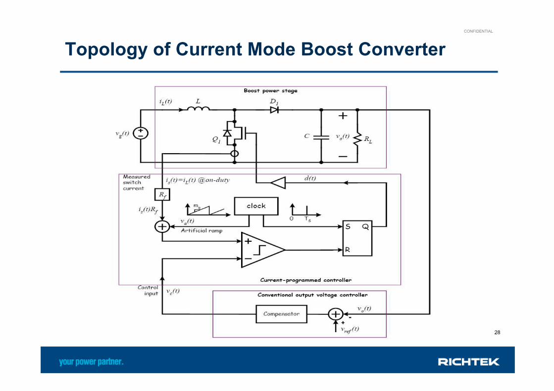
Topology of Current Mode Boost Converter

CONFIDENTIAL
29
System Block & Average ModelingSystem Block & Average Modeling
• Am example: a NAVPTM multi-phase system block & Small signal modeling
LLR
2RiAvGain ==
Vref
Zo
Gvd
Gii
Gid
Fm
Gci
LPF
Gcv
- -
VoIo
iL
compcomp2
vcs
*Published at 2007 PESC

CONFIDENTIAL
30
Calculation Results by MathCAD Results by MathCAD
•Output impedance & Loop gain calculation using MathCAD
1 10 100 1 .103
1 .104
1 .105
1 .106
50
0
50
100
Gain of Loop (LGCM AVP)
Frequency (Hz)
Gain (dB)
MathCAD_loop j( )
f j( )
1 10 100 1 .103
1 .104
1 .105
1 .106
120
110
100
90
80
Phase of Loop (LGCM AVP)
Frequency (Hz)
Phase (degree)
MathCAD_loop j( )
f j( )

CONFIDENTIAL
31
SimplisSimplis Behavior Modeling Behavior Modeling
Mode Transition
Load Transient

CONFIDENTIAL
32
Energy Transferring Element
dt
diLv =
i
−+v
∫∫ ×=×=×= 2
2
1iL
dt
diLiviWm

CONFIDENTIAL
33
Power IC Technology
BiCMOS
*Referred from Tsmc

CONFIDENTIAL
34
Product Design Kit
*Referred from Tsmc

CONFIDENTIAL
35
High Performance Analog Process
DDD MOS
LDMOS
DMOS
BJT
Diode

CONFIDENTIAL
36
Voltage Trend
0.3V 0.6V 1V 3.3V 5V 12V 19V 30V 60V 100V 500V 600V
PV Solar cell
1 cell Ni-MH
1 cell Li-ion
ATX main power
2 cell Li-ion & 19V Adapter in
AC <30W Adapter/charger
Offline PFC power supply
Offline ATX power supply
WLED driver
Sync high side MOS driver
-48V POE
USB 5V
TFT LCD Panel

CONFIDENTIAL
37
LDO
• Low dropout voltage
• Low quiescent current
• Low output noise
• High PSRR
• Fast transient response
• 1uF ceramic stable
• Full protection
• Low cost, poor efficiency

CONFIDENTIAL
38
LDO IC
RT9193
tsmc 0.6um

CONFIDENTIAL
39
Voltage Mode Buck Controller
• Wide input range
• Synchronous driver
• Bootstrap driver
• Variable modulation gain
• Soft start
• Full protection

CONFIDENTIAL
40
PWM IC
UG Driver
LG Driver
Vref
Error Amp
OSC
PWM CP
Level Shift
RT9214

CONFIDENTIAL
41
Current Mode Buck Converter
• Synchronous rectifier
• High frequency >1MHz
• Internal compensation
• Small output LC
• High efficiency 95%
• Small package

CONFIDENTIAL
42
Current Mode Boost Converter
• Small output LC
• High frequency >1MHz
• Easy stable
• High efficiency 95%
• Small package

CONFIDENTIAL
43
RT9277

CONFIDENTIAL
44
Charge Pump
• Small size with ceramic capacitor only
• X1,x1.5 or 2x pump
• High frequency >1MHz
• Dimming operation
• Small package

CONFIDENTIAL
45
Charge Pump IC
RT9361

CONFIDENTIAL
46
DSC Multi-Channel PMU

CONFIDENTIAL
47
RT9917 Die Photograph

CONFIDENTIAL
48
RT9917 Demo Board Demo Board Photograph

CONFIDENTIAL
49
Multi-phase Multi-loop Control
Current
Balance
Processor
+_
+_
PWM Logic
& Driver
PWM Logic
& Driver
+_
+_
+_
Droop
Control
SS
Control
ISP1
ISN1
ISP2
ISN2
VDAC
GND
CS1
CS2
PWMCP
PWMCPEA
RT9600
RT9600
VIN
VINCOUTRLOAD
PWM1
PWM2
FB
ADJ
COMP SS
Voltage
loopCurrent
loop
Current
Balance
Processor
+_
+_
PWM Logic
& Driver
PWM Logic
& Driver
+_
+_
+_
Droop
Control
SS
Control
ISP1
ISN1
ISP2
ISN2
VDAC
GND
CS1
CS2
PWMCP
PWMCPEA
RT9600
RT9600
VIN
VINCOUTRLOAD
PWM1
PWM2
FB
ADJ
COMP SS
Current
Balance
Processor
+_
+_
PWM Logic
& Driver
PWM Logic
& Driver
PWM Logic
& Driver
PWM Logic
& Driver
+_+
_+
_+
_
+_
+_
Droop
Control
Droop
Control
SS
Control
SS
Control
ISP1
ISN1
ISP2
ISN2
VDAC
GND
CS1
CS2
PWMCP
PWMCPEA
RT9600RT9600
RT9600RT9600
VIN
VINCOUTRLOAD
PWM1
PWM2
FB
ADJ
COMP SS
Voltage
loopCurrent
loop
VGS (MAIN SW ITCH OF MODULE 1)
VGS (MAIN SW ITCH OF MODULE 2)
VER
IO/2
IL1
IL2
IC
IO
0 DT T
∆
Active voltage loop• Split Multiphase
• Multi loop control
• Current balance
• Active voltage droop

CONFIDENTIAL
50
Multiphase PWM VRM
VIN
VIN
VIN
VIN
Vout

CONFIDENTIAL
51
Digital PWM (經濟部業界科專計畫經濟部業界科專計畫經濟部業界科專計畫經濟部業界科專計畫 “數位電源管理系統單晶片數位電源管理系統單晶片數位電源管理系統單晶片數位電源管理系統單晶片” )
Analog power mimic•Take advantage of nanoprocess VLSI
•Performance close to analog
• Evolution of DPWM in Richtek
13K Gates0.25um CMOS
0.22 mm2
No External Components
Digital Filter Equivalent
Power
SupplyVINVOUT
GUIPMBusUSB
Power
SupplyVINVOUT
GUIPMBus
OR
PC
More function than analog power• Configuration by PMBus protocol
• Programmable (sequencing, Vo)
• Monitoring (fault)
• Performance close to analog power w/ more functions
Smart Power• Higher efficiency & faster response
• Power OS: Self-tuning/diagnosis
• Performance/functions beyond analog power

CONFIDENTIAL
52
Team Work for Customer Oriented
Customer
Sales FAE TME CS
AE
RD PDK
PMEPC
PE TE
QA

CONFIDENTIAL
53
Silicon Implementation & System SetupSilicon Implementation & System Setup
Vin
VinProcessor
Load
L1=0.36uH
L2=0.36uH
Co
RT8851
Q1
Q2
Q3
Q4
0.36uHInductor
10uFx22MLCC
330uFx4POSCAP
BSC032N03SGLS-MOSFET
BSC094N03SGHS-MOSFET
~44AIOUT
7V~21VVIN
2-PH NAVPTM w/ 2 driversController

CONFIDENTIAL
54
Promotion Kits Promotion Kits –– Design ToolDesign Tool

CONFIDENTIAL
55
Demo Board I Demo Board I

CONFIDENTIAL
56
13-Channel PMU with I2C and USB TXR

CONFIDENTIAL
57
RT9926 Demo System Control Flow
USB CONNECT
OE#
SPD
RCV
VP
SUS
VM
VBUS
VTRM
D+
D-
GND
SIE
CONTROLLER
USB-I2
C
BRIDGE
VCC GND
ON/OFF CONTROL&
I2C INTERFACE
LDO10
LDO2
LDO3
LDO4
LDO5
LDO1
LDO9
LDO8
LDO7
LDO6
Buck1
Buck2
RT9904 PMICRT9904 PMICRT9904 PMICRT9904 PMIC
VBAT
USB Xceiver
SCL
SDA
PWR_ON
RT9926 GUI
RT9926 PMIC

CONFIDENTIAL
58
RT9926 GUI
GUI for easy Control
USB communication for popular connection

CONFIDENTIAL
59
Package Trend
Flip chip
SO series
19919988~2000~2000 20022002 20042004 20020066 20020088
Dual row
QFN
COL
TSSOP
TQF
P
Power QFN
WL-CSP
MCM QFN
SOT
DDPAK
TSOT
QFN/DFNV-type
QFN/DFNX-type
QFN/DFNW-type
S
C
High
Performance
High
Performance
Low R_onLow R_on
High DensityHigh Density
SIP

CONFIDENTIAL
60
QFN Package
QFN
• Reduce electrical parasitic
• Lower thermal resistance
• Improved board space efficiency
• Reduced mounted height
• Reduced package mass

CONFIDENTIAL
61
WLCSP
WLCSP-I
WLCSP-II
• Reduce electrical parasitic
• Chip scale size
• Improved board space efficiency
• Reduced mounted height
• Reduced package mass

CONFIDENTIAL
62
Reliability and Qualification
• ESD
• Latch-up
• Surge
• Plug in Spiking
• Current Spike
• Noise Injection
• Electron Migration
• EMI
• Process qual.
• Package qual.
• Alpha site test
• Beta site test
• Final Test
• Temperature test
• OLT burn in

CONFIDENTIAL
63
Failure Analysis -- I
• VCOM to AGND BGND to AGND ESD cell
CONFIDENTIAL
64
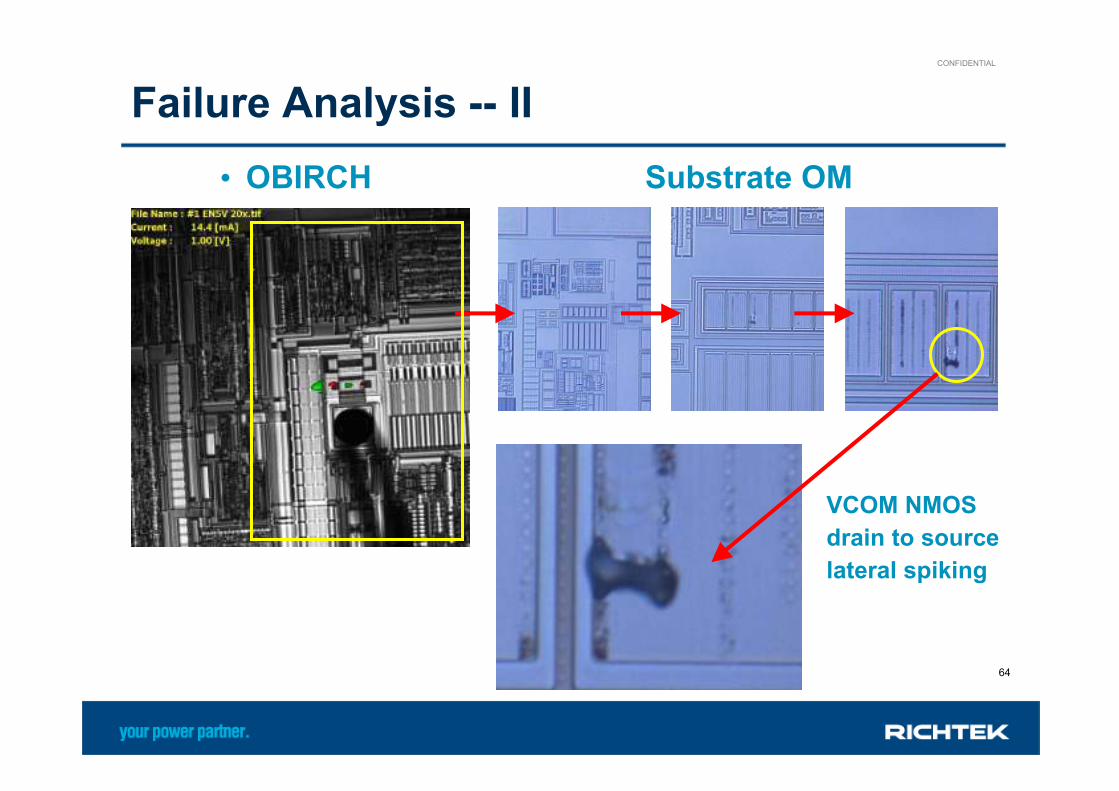
Failure Analysis -- II
• OBIRCH Substrate OM
VCOM NMOS
drain to source
lateral spiking

CONFIDENTIAL
65
Failure Analysis -- III
The damage site is
similar to return sample

CONFIDENTIAL
66
Summary
• Power IC industry is mutual in TW
• Foundry process technology is available
• Own system topology design capability
• Own silicon circuit design capability
• Promotion kit service is available
• Quality and reliability have been proven

CONFIDENTIAL
67
Http://www.richtek.com
CONFIDENTIAL
68
Contest for Power Management IC Design & System Application

CONFIDENTIAL
69
Contest for Power Management IC Design & System Application


![TIN & Surface Interpolationweb.pdx.edu/~jduh/courses/geog493f12/Week06.pdfMicrosoft PowerPoint - Week06.ppt [Compatibility Mode] Author jduh Created Date 10/29/2012 6:25:57 PM](https://img.pdfslide.net/doc/110x75/5f832bbbe5e1454be4340ebc/tin-surface-jduhcoursesgeog493f12week06pdf-microsoft-powerpoint-week06ppt.jpg)

![Seminář2008-úvod tisk [Režim kompatibility]old.botany.upol.cz/prezentace/sedlarova/Seminar2008.pdf · 2008. 11. 20. · sbírka mikroorganismů pro standardní metody biotestace](https://img.pdfslide.net/doc/110x75/5fbc4ea3cd33dd0a4f78dedc/semin2008-vod-tisk-reim-kompatibilityold-2008-11-20-sbrka-mikroorganism.jpg)