Embed Size (px)
Citation preview

Introduction to Assembly Language Programming

Overview of Assembly Language
Advantages:
Disadvantages:
Faster as compared to programs written using high-level languages
Efficient memory usage
Control down to bit level
× Need to know detail hardware implementation
× Not portable
× Slow to development and difficult to debug
Basic components in assembly Language:
Instruction, Directive, Label, and Comment

8086/8088 Internal Organisation
T e m p o ra ryR e g is te rs
A L U
F la g s
E UC o n tro l
A H A L
B H B L
C H C L
D H D L
S P
B P
D I
B I
C S
D S
S S
E S
IO
In te rn a lC o m m u n ic a t io n s
R e g is te rs
S U M M A T IO N
A d d re s s B u s 2 0 b its
D a ta B u s
B u sC o n tro l
1 2 3 4
In s t ru c t io n Q u e u e
8 0 8 8B u s
E U B IU

BIU Elements• Instruction Queue: the next instructions or data can be fetched
from memory while the processor is executing the current instruction– The memory interface is slower than the processor execution time so
this speeds up overall performance
• Segment Registers: – CS, DS, SS and ES are 16b registers
– Used with the 16b Base registers to generate the 20b address
– Allow the 8086/8088 to address 1MB of memory
– Changed under program control to point to different segments as a program executes
• Instruction Pointer (IP) contains the Offset Address of the next instruction, the distance in bytes from the address given by the current CS register

8086/8088 20-bit Addresses
1 6 - b i t S e g n m e n t B a s e A d d r e s s 0 0 0 0
1 6 - b i t O f f s e t A d d r e s s
2 0 - b i t P h y s i c a l A d d r e s s
C S
I P

Exercise: 20-bit Addressing
1. CS contains 0A820h,IP contains 0CE24h. What is the resulting physical address?
2. CS contains 0B500h, IP contains 0024h. What is the resulting physical address?

Example of Assembly Language Program
;NUMOFF.ASM: Turn NUM-LOCK indicator off.
.MODEL SMALL
.STACK
.CODE
.STARTUP
MOV AX,40H ;set AX to 0040H
D1: MOV DS,AX ;load data segment with 0040H
MOV SI,17H ;load SI with 0017H
AND BYTE PTR [SI],0DFH ;clear NUM-LOCK bit
.EXIT
END
Comments
Assembly directive
Instructions
Assembly directive
Label

Instruction Format
General Format of Instructions
Label: Opcode Operands ; Comment
Label: It is optional. It provides a symbolic address that can be used in branch instructions
Opcode: It specifies the type of instructions
Operands: Instructions of 80x86 family can have one, two, or zero operand
Comments: Only for programmers’ reference
Machine Code Format
Opcode Operand1Mode Operand2
1 0 0 0 1 0 0 0 1 1 0 0 0 0 1 1MOV AL, BL
MOVRegistermode

What is the Meaning of Addressing Modes?
When a CPU executes an instruction, it needs to know where to get data and where to store results. Such information is specified in the operand fields of the instruction.
1 0 0 0 1 0 0 0 1 1 0 0 0 0 1 1 MOV AL, BL
Opcode Mode Operand1 Operand2
An operand can be:— A datum— A register location— A memory location
Addressing modes define how the CPU finds where to get data and where to store results

Immediate Addressing
Data needed by the processor is contained in the instruction
For Example: move 7 to register AL
MOV AL, 7 AH
AL
7
Machine code of MOV AL, 7
1 0 1 1 0 0 0 0 0 0 0 0 0 1 1 1
7AL
Indicate 8-bit data operation
Move an immediate datum to a register

Register Addressing
Operands of the instruction are the names of internal register The processor gets data from the register locations specified by instruction operands
For Example: move the value of register BL to register AL
MOV AL, BL AH
BH
AL
BL
If AX = 1000H and BX=A080H, after the execution of MOV AL, BL what are the new values of AX and BX?
In immediate and register addressing modes, the processor does not access memory.Thus, the execution of such instructions are fast.

Direct Addressing
The processor accesses a memory location The memory location is determined by the value of segment register DS and the displacement (offset) specified in the instruction operand field
DS × 10H + Displacement = Memory location
— Example: assume DS = 1000H, AX = 1234H
MOV [7000H], AX
AH AL
3412 17001H
17000H34
12
DS: 1 0 0 0 _+ Disp: 7 0 0 0
1 7 0 0 0

Register Indirect Addressing
One of the registers BX, BP, SI, DI appears in the instruction operand field. Its value is used as the memory displacement value.
For Example: MOV DL, [SI]
Memory address is calculated as following:
DS
SS
× 10H +
BXSIDI
BP
= Memory address
If BX, SI, or DI appears in the instruction operand field, segment register DS is used in address calculation If BP appears in the instruction operand field, segment register SS is used in address calculation

Register Indirect Addressing
Example 1: assume DS = 0800H, SI=2000H
MOV DL, [SI]
120A000H
DH DL12
DS: 0 8 0 0 _+ SI: 2 0 0 0
0 A 0 0 0
Example 2: assume SS = 0800H, BP=2000H, DL = 7
MOV [BP], DL
memory

Based Addressing
The operand field of the instruction contains a base register (BX or BP) and an 8-bit (or 16-bit) constant (displacement)
For Example: MOV AX, [BX+4]
Calculate memory address
DS
SS
× 10H + + Displacement = Memory address
If BX appears in the instruction operand field, segment register DS is used in address calculation If BP appears in the instruction operand field, segment register SS is used in address calculation
BX
BP
What’s difference between register indirect addressing and based addressing?

Based Addressing
Example 1: assume DS = 0100H, BX=0600H
MOV AX, [BX+4]
B001604H
AH ALB0
DS: 0 1 0 0 _+ BX: 0 6 0 0+ Disp.: 0 0 0 4
0 1 6 0 4
Example 2: assume SS = 0A00H, BP=0012H, CH = ABH
MOV [BP-7], CH
01605H C0
C0
memory

Indexed Addressing
The operand field of the instruction contains an index register (SI or DI) and an 8-bit (or 16-bit) constant (displacement)
For Example: MOV [DI-8], BL
Calculate memory address
DS × 10H + + Displacement = Memory address
SI
DI
Example: assume DS = 0200H, DI=0030H BL = 17H
MOV [DI-8], BL
DS: 0 2 0 0 _+ DI: 0 0 3 0- Disp.: 0 0 0 8
0 2 0 2 8
BH BL17
17 02028H
memory

Based Indexed Addressing
The operand field of the instruction contains a base register (BX or BP) and an index register
For Example: MOV [BP] [SI], AHMOV [BP+SI], AH
Calculate memory address
DS
SS
× 10H + + {SI or DI} = Memory address
If BX appears in the instruction operand field, segment register DS is used in address calculation If BP appears in the instruction operand field, segment register SS is used in address calculation
BX
BP
or

Based Indexed Addressing
Example 1: assume SS = 2000H, BP=4000H, SI=0800H, AH=07H
MOV [BP] [SI], AHAH AL
SS: 2 0 0 0 _+ BP: 4 0 0 0+ SI.: 0 8 0 0
2 4 8 0 0
Example 2: assume DS = 0B00H, BX=0112H, DI = 0003H, CH=ABH
MOV [BX+DI], CH
24800H 07
07
memory

Based Indexed with Displacement Addressing
The operand field of the instruction contains a base register (BX or BP), an index register, and a displacement
For Example: MOV CL, [BX+DI+2080H]
Calculate memory address
DS
SS
× 10H + + {SI or DI} + Disp. = Memory address
If BX appears in the instruction operand field, segment register DS is used in address calculation If BP appears in the instruction operand field, segment register SS is used in address calculation
BX
BP

Based Indexed with Displacement Addressing
Example 1: assume DS = 0300H, BX=1000H, DI=0010H
MOV CL, [BX+DI+2080H]CH CL
DS: 0 3 0 0 _+ BX: 1 0 0 0+ DI.: 0 0 1 0+ Disp. 2 0 8 0
0 6 0 9 0
Example 2: assume SS = 1100H, BP=0110H, SI = 000AH, CH=ABH
MOV [BP+SI+0010H], CH
06090H 20
memory
20

Instruction Types
Data transfer instructions
String instructions
Arithmetic instructions
Bit manipulation instructions
Loop and jump instructions
Subroutine and interrupt instructions
Processor control instructions
An excellent website about 80x86 instruction set: http://www.penguin.cz/~literakl/intel/intel.htmlAnother good reference is in the tutorial of 8086 emulator

Addressing Modes
Immediate addressing MOV AL, 12H
Register addressing MOV AL, BL
Direct addressing MOV [500H], AL
Register Indirect addressing MOV DL, [SI]
Based addressing MOV AX, [BX+4]
Indexed addressing MOV [DI-8], BL
Based indexed addressing MOV [BP+SI], AH
Based indexed with displacement addressing MOV CL, [BX+DI+2]
Exceptions String addressing
Port addressing (e.g. IN AL, 79H)
Addressing Modes Examples

Flag Register
OF DF IF TF ZFSF AF PF CF
015
Control Flags Status Flags
IF: Interrupt enable flagDF: Direction flagTF: Trap flag
CF: Carry flagPF: Parity flagAF: Auxiliary carry flagZF: Zero flagSF: Sign flagOF: Overflow flag
Flag register contains information reflecting the current status of a microprocessor. It also contains information which controls the operation of the microprocessor.

Flags Commonly Tested During the Execution of Instructions
There are five flag bits that are commonly tested during the execution of instructions
Sign Flag (Bit 7), SF: 0 for positive number and 1 for negative number
Zero Flag (Bit 6), ZF: If the ALU output is 0, this bit is set (1); otherwise, it is 0
Carry Flag (Bit 0), CF: It contains the carry generated during the execution
Auxiliary Carry, AF: Depending on the width of ALU inputs, this flag (Bit 4) bit contains the carry generated at bit 3 (or, 7, 15) of the 8088 ALU
Parity Flag (bit2), PF: It is set (1) if the output of the ALU has even number of ones; otherwise it is zero

Data Transfer Instructions
MOV Destination, Source
— Move data from source to destination; e.g. MOV [DI+100H], AH
For 80x86 family, directly moving data from one memory location to another memory location is not allowed
MOV [SI], [5000H]
When the size of data is not clear, assembler directives are used
MOV [SI], 0
BYTE PTR MOV BYTE PTR [SI], 12H WORD PTR MOV WORD PTR [SI], 12H DWORD PTR MOV DWORD PTR [SI], 12H
— It does not modify flags
You can not move an immediate data to segment register by MOV
MOV DS, 1234H

Instructions for Stack Operations
What is a Stack ?— A stack is a collection of memory locations. It always follows the rule of last-in-firs-out— Generally, SS and SP are used to trace where is the latest date written into stack
PUSH Source
— Push data (word) onto stack— It does not modify flags— For Example: PUSH AX (assume ax=1234H, SS=1000H, SP=2000H before PUSH AX)
1000:2000
1000:1FFF
1000:1FFE
1000:1FFD
??
??
??
??
1000:2000
1000:1FFF
1000:1FFE
1000:1FFD
??
12
34
??
SS:SP
SS:SP
Before PUSH AX, SP = 2000H After PUSH AX, SP = 1FFEH AX
12 34
Decrementing the stack pointer during a push is a standard way of implementing stacks in hardware

Instructions for Stack Operations PUSHF
— Push the values of the flag register onto stack— It does not modify flags
POP Destination
1000:2000
1000:1FFF
1000:1FFE
1000:1FFD
EC
12
34
??
1000:2000
1000:1FFF
1000:1FFE
1000:1FFD
EC
12
34
??
SP
SP
Before POP, SP = 1FFEH After POP AX, SP = 2000H AX
12 34
— Pop word off stack— It does not modify flags— For example: POP AX
POPF — Pop word from the stack to the flag register— It modifies all flags

Data Transfer Instructions
SAHF
LAHF
— Store data in AH to the low 8 bits of the flag register— It modifies flags: AF, CF, PF, SF, ZF
— Copies bits 0-7 of the flags register into AH— It does not modify flags
LDS Destination Source
— Load 4-byte data (pointer) in memory to two 16-bit registers— Source operand gives the memory location — The first two bytes are copied to the register specified in the destination operand; the second two bytes are copied to register DS — It does not modify flags
LES Destination Source
— It is identical to LDS except that the second two bytes are copied to ES— It does not modify flags

Data Transfer Instructions LEA Destination Source
— Transfers the offset address of source (must be a memory location) to the destination register— It does not modify flags
XCHG Destination Source
— It exchanges the content of destination and source— One operand must be a microprocessor register, the other one can be a register or a memory location — It does not modify flags
XLAT
— Replace the data in AL with a data in a user defined look-up table— BX stores the beginning address of the table— At the beginning of the execution, the number in AL is used as the index of the look-up table — It does not modify flags

String Instructions String is a collection of bytes, words, or long-words that can be up to 64KB in length
String instructions can have at most two operands. One is referred to as source string and the other one is called destination string
— Source string must locate in Data Segment and SI register points to the current element of the source string — Destination string must locate in Extra Segment and DI register points to the current element of the destination string
53
48
4F
50
50
45
S
H
O
PP
52
E
R
0510:0000
0510:0001
0510:0002
0510:0003
0510:00040510:0005
0510:0006
53
48
4F
50
50
49
S
H
O
PP
4E
I
N
02A8:2000
02A8:2001
02A8:2002
02A8:2003
02A8:200402A8:2005
02A8:2006
DS : SI ES : DI
Source String Destination String

Repeat Prefix Instructions REP String Instruction
— The prefix instruction makes the microprocessor repeatedly execute the string instruction until CX decrements to 0 (During the execution, CX is decreased by one when the string instruction is executed one time).
— For Example:
MOV CX, 5REP MOVSB
By the above two instructions, the microprocessor will execute MOVSB 5 times.
— Execution flow of REP MOVSB::
While (CX!=0) { CX = CX –1; MOVSB; }
Check_CX: If CX!=0 Then CX = CX –1; MOVSB; goto Check_CX; end if
OR

Repeat Prefix Instructions REPZ String Instruction
— Repeat the execution of the string instruction until CX=0 or zero flag is clear
REPNZ String Instruction
— Repeat the execution of the string instruction until CX=0 or zero flag is set
REPE String Instruction
— Repeat the execution of the string instruction until CX=0 or zero flag is clear
REPNE String Instruction
— Repeat the execution of the string instruction until CX=0 or zero flag is set

Direction Flag Direction Flag (DF) is used to control the way SI and DI are adjusted during the execution of a string instruction
— DF=0, SI and DI will auto-increment during the execution; otherwise, SI and DI auto-decrement
— Instruction to set DF: STD; Instruction to clear DF: CLD
— Example:
CLDMOV CX, 5REP MOVSB
At the beginning of execution,DS=0510H and SI=0000H
53
48
4F
50
50
45
S
H
O
PP
52
E
R
0510:0000
0510:0001
0510:0002
0510:0003
0510:00040510:0005
0510:0006
DS : SI
Source String
SI CX=5
SI CX=4
SI CX=3
SI CX=2
SI CX=1
SI CX=0
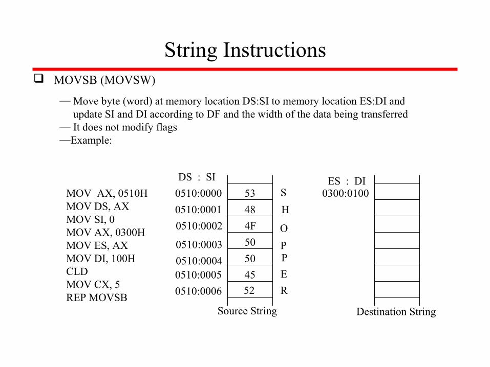
String Instructions MOVSB (MOVSW)
— Move byte (word) at memory location DS:SI to memory location ES:DI and update SI and DI according to DF and the width of the data being transferred— It does not modify flags—Example:
53
48
4F
50
50
45
S
H
O
PP
52
E
R
0510:0000
0510:0001
0510:0002
0510:0003
0510:00040510:0005
0510:0006
0300:0100
DS : SI ES : DI
Source String Destination String
MOV AX, 0510HMOV DS, AXMOV SI, 0MOV AX, 0300HMOV ES, AXMOV DI, 100HCLDMOV CX, 5REP MOVSB

String Instructions CMPSB (CMPSW)
— Compare bytes (words) at memory locations DS:SI and ES:DI; update SI and DI according to DF and the width of the data being compared— It modifies flags—Example:
Assume: ES = 02A8HDI = 2000HDS = 0510HSI = 0000H
CLDMOV CX, 9REPZ CMPSB
What’s the values of CX afterThe execution?
53
48
4F
50
50
45
S
H
O
PP
52
E
R
0510:0000
0510:0001
0510:0002
0510:0003
0510:00040510:0005
0510:0006
02A8:2000
DS : SIES : DI
Source String Destination String
02A8:2001
02A8:2002
02A8:2003
02A8:2004
02A8:200502A8:2006
53
48
4F
50
50
49
S
H
O
PP
4E
I
N

String Instructions SCASB (SCASW)
— Move byte (word) in AL (AX) and at memory location ES:DI; update DI according to DF and the width of the data being compared— It modifies flags
LODSB (LODSW)
— Load byte (word) at memory location DS:SI to AL (AX); update SI according to DF and the width of the data being transferred— It does not modify flags
STOSB (STOSW)
— Store byte (word) at in AL (AX) to memory location ES:DI; update DI according to DF and the width of the data being transferred— It does not modify flags

Arithmetic Instructions
ADD Destination, Source
— Destination + Source Destination— Destination and Source operands can not be memory locations at the same time— It modifies flags AF CF OF PF SF ZF
ADC Destination, Source
— Destination + Source + Carry Flag Destination— Destination and Source operands can not be memory locations at the same time— It modifies flags AF CF OF PF SF ZF
INC Destination— Destination + 1 Destination— It modifies flags AF OF PF SF ZF (Note CF will not be changed)
DEC Destination— Destination - 1 Destination
— It modifies flags AF OF PF SF ZF (Note CF will not be changed)

Arithmetic Instructions
SUB Destination, Source— Destination - Source Destination— Destination and Source operands can not be memory locations at the same time— It modifies flags AF CF OF PF SF ZF
SBB Destination, Source
— Destination - Source - Carry Flag Destination— Destination and Source operands can not be memory locations at the same time— It modifies flags AF CF OF PF SF ZF
CMP Destination, Source
— Destination – Source (the result is not stored anywhere)— Destination and Source operands can not be memory locations at the same time— It modifies flags AF CF OF PF SF ZF (if ZF is set, destination = source)

Arithmetic Instructions
MUL Source
— Perform unsigned multiply operation— If source operand is a byte, AX = AL * Source— If source operand is a word, (DX AX) = AX * Source— Source operands can not be an immediate data— It modifies CF and OF (AF,PF,SF,ZF undefined)
IMUL Source
— Perform signed binary multiply operation— If source operand is a byte, AX = AL * Source— If source operand is a word, (DX AX) = AX * Source— Source operands can not be an immediate data— It modifies CF and OF (AF,PF,SF,ZF undefined)
Examples: MOV AL, 20HMOV CL, 80HMUL CL
MOV AL, 20HMOV CL, 80HIMUL CL

DIV Source
— Perform unsigned division operation— If source operand is a byte, AL = AX / Source; AH = Remainder of AX / Source— If source operand is a word, AX=(DX AX)/Source; DX=Remainder of (DX AX)/Source— Source operands can not be an immediate data
IDIV Source
Examples: MOV AX, 5MOV BL, 2DIV BL
MOV AL, -5MOV BL, 2IDIV BL
Arithmetic Instructions
— Perform signed division operation— If source operand is a byte, AL = AX / Source; AH = Remainder of AX / Source— If source operand is a word, AX=(DX AX)/Source; DX=Remainder of (DX AX)/Source— Source operands can not be an immediate data

Arithmetic Instructions NEG Destination
— 0 – Destination Destination (the result is represented in 2’s complement)— Destination can be a register or a memory location— It modifies flags AF CF OF PF SF ZF
CBW — Extends a signed 8-bit number in AL to a signed 16-bit data and stores it into AX — It does not modify flags
CWD — Extends a signed 16-bit number in AX to a signed 32-bit data and stores it into DX and AX. DX contains the most significant word — It does not modify flags
Other arithmetic instructions:
DAA, DAS, AAA, AAS, AAM, AAD

Logical Instructions NOT Destination
— Inverts each bit of the destination operand— Destination can be a register or a memory location— It does not modify flags
AND Destination, Source— Performs logic AND operation for each bit of the destination and source; stores the result into destination— Destination and source can not be both memory locations at the same time— It modifies flags: CF OF PF SF ZF
OR Destination, Source— Performs logic OR operation for each bit of the destination and source; stores the result into destination— Destination and source can not be both memory locations at the same time— It modifies flags: CF OF PF SF ZF

Logical Instructions
XOR Destination, Source— Performs logic XOR operation for each bit of the destination and source; stores the result into destination— Destination and source can not be both memory locations at the same time— It modifies flags: CF OF PF SF ZF
TEST Destination, Source— Performs logic AND operation for each bit of the destination and source— Updates Flags depending on the result of AND operation— Do not store the result of AND operation anywhere

Bit Manipulation Instructions
SHL(SAL) Destination, Count— Left shift destination bits; the number of bits shifted is given by operand Count— During the shift operation, the MSB of the destination is shifted into CF and zero is shifted into the LSB of the destination— Operand Count can be either an immediate data or register CL— Destination can be a register or a memory location— It modifies flags: CF OF PF SF ZF
CF 0
SHR Destination, Count— Right shift destination bits; the number of bits shifted is given by operand Count— During the shift operation, the LSB of the destination is shifted into CF and zero is shifted into the MSB of the destination— Operand Count can be either an immediate data or register CL— Destination can be a register or a memory location— It modifies flags: CF OF PF SF ZF
CF0 Destination
Destination
LSBMSB
LSBMSB

Bit Manipulation Instructions
SAR Destination, Count
— Right shift destination bits; the number of bits shifted is given by operand Count— The LSB of the destination is shifted into CF and the MSB of the destination remians the same— Operand Count can be either an immediate data or register CL— Destination can be a register or a memory location— It modifies flags: CF PF SF ZF
CFDestination
LSBMSB

Bit Manipulation Instructions ROL Destination, Count
— Left shift destination bits; the number of bits shifted is given by operand Count— The MSB of the destination is shifted into CF, it also goes to the LSB of the destination— Operand Count can be either an immediate data or register CL— Destination can be a register or a memory location— It modifies flags: CF OF
CF Destination
ROR Destination, Count— Right shift destination bits; the number of bits shifted is given by operand Count— The LSB of the destination is shifted into CF, it also goes to the MSB of the destination— Operand Count can be either an immediate data or register CL— Destination can be a register or a memory location— It modifies flags: CF OF
CFDestination
LSBMSB
LSBMSB

Bit Manipulation Instructions RCL Destination, Count
— Left shift destination bits; the number of bits shifted is given by operand Count— The MSB of the destination is shifted into CF; the old CF value goes to the LSB of the destination— Operand Count can be either an immediate data or register CL— Destination can be a register or a memory location— It modifies flags: CF OF PF SF ZF
CF Destination
RCR Destination, Count— Right shift destination bits; the number of bits shifted is given by operand Count— The LSB of the destination is shifted into CF, the old CF value goes to the MSB of the destination— Operand Count can be either an immediate data or register CL— Destination can be a register or a memory location— It modifies flags: CF OF PF SF ZF
CFDestination
LSBMSB
LSBMSB

Program Transfer Instructions JMP Target
— Unconditional jump— It moves microprocessor to execute another part of the program — Target can be represented by a label, immediate data, registers, or memory locations — It does not affect flags
The execution of JMP instruction
JMP 1234H : 2000H
CS
IP
1234H
2000H
14340HNext Instruction Address
JMP
Current instruction
Next instruction
Jump

Program Transfer Instructions Intrasegment transfer v.s. Intersegment transfer
— Intrasegment transfer: the microprocessor jumps to an address within the same segment— Intersegment transfer: the microprocessor jumps to an address in a difference segment— Use assembler directive near and far to indicate the types of JMP instructions
— For intrasegment transfer, we can provide only new IP value in JMP instructions. For Example: JMP 1000H— For intersegment transfer, we need provide both new CS and IP values in JMP instructions For Example: JMP 2000H : 1000H
Direct Jump v.s. Indirect Jump— Direct Jump: the target address is directly given in the instruction — Indirect Jump: the target address is contained in a register or memory location
Short Jump
— If the target address is within +127 or –128 bytes of the current instruction address, the jump is called a short jump— For short jumps, instead of specifying the target address, we can specify the relative offset (the distance between the current address and the target address) in JMP instructions.
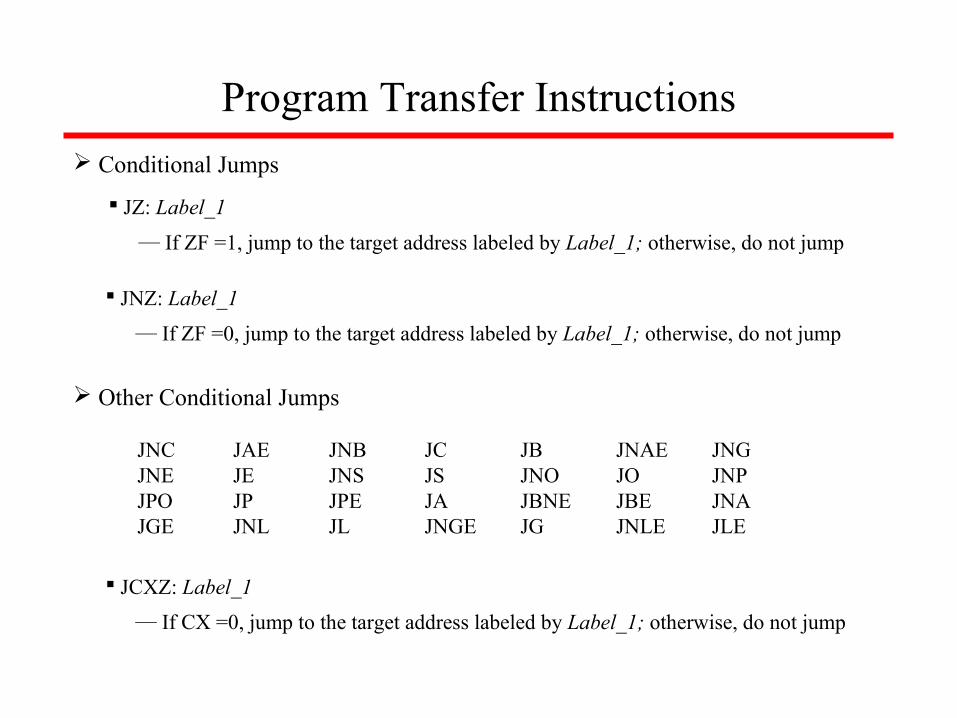
Program Transfer Instructions Conditional Jumps
JZ: Label_1
— If ZF =1, jump to the target address labeled by Label_1; otherwise, do not jump
JNZ: Label_1
— If ZF =0, jump to the target address labeled by Label_1; otherwise, do not jump
Other Conditional Jumps
JNC JAE JNB JC JB JNAE JNGJNE JE JNS JS JNO JO JNPJPO JP JPE JA JBNE JBE JNAJGE JNL JL JNGE JG JNLE JLE
JCXZ: Label_1
— If CX =0, jump to the target address labeled by Label_1; otherwise, do not jump

Program Transfer Instructions LOOP Short_Label
— It is limited for short jump— Execution Flow:
CX = CX –1If CX != 0 Then JMP Short_LabelEnd IF
LOOPE/LOOPZ Short_Label
CX = CX –1If CX != 0 & ZF=1 Then JMP Short_LabelEnd IF
LOOPNE/LOOPNZ Short_LabelCX = CX –1If CX != 0 & ZF=0 Then JMP Short_LabelEnd IF

Processor Control Instructions
CLC Clear carry flag
STC Set carry flag
CMC Complement carry flag
CLD Clear direction flag
STD Set direction flag
CLI Clear interrupt-enable flag
STI Set interrupt-enable flag
HLT Halt microprocessor operation
NOP No operation
LOCK Lock Bus During Next Instruction

Subroutine Instructions
A subroutine is a collection of instructions that can be called from one or more other locations within a program
CALL Procedure-Name
• • •MOV AL, 1CALL M1MOV BL, 3• • •M PROC MOV CL, 2 RETM ENDP
— Example
The order of execution:
MOV AL, 1MOV CL, 2MOV BL, 3
— Intersegment CALL: the subroutine is located in a different code segment— Intrasegment CALL: the subroutine is located in the same code segment— Use assembler directives far and near to distinguish intersegment and intrasegment CALL

Subroutine Instructions
What does the microprocessor do when it encounters a CALL instruction?
1. Push the values of CS and IP (which specify the address of the instruction immediatelyfollowing the CALL instruction) into stack. If it is a intrasegment CALL, just push the value of IP into stack.
2. Load the new values to CS and IP such that the next instruction that the microprocessor will fetch is the first instruction of the subroutine
.model small 0000 .code 0000 B0 02 MOV AL, 2 0002 E8 0002 CALL m1 0005 B3 03 MOV BL, 3
0007 m1 Proc 0007 B7 05 MOV BH, 5 0009 C3 RET 000A m1 ENDP end
— Example:
12345H
Stack before CALL
What are in the stackafter the execution of CALL?
How about if the CALL is an intersegmentCALL?
11

Subroutine Instructions
RET — It lets the microprocessor exit from a subroutine— If it is used in a FAR procedure, RET pops two words from the stack. The first one goes to IP register. The second one goes to CS register— If it is used in a NEAR procedure, RET pops one word from stack to IP register
1234:2345 •••1234:2348 CALL FAR PTR M11234:234D •••
M1 PROC FAR3456:0120 MOV AL, 0 ••• RET M1 ENDP
— Example:
01022
What data are pushedinto and popped from the stack during the execution of CALL and RET?

Interrupt Instructions
INT Interrupt-Type
— This instruction causes the microprocessor to execute an interrupt service routine. The Interrupt-Type is an immediate data (0-255) which specifies the type of interrupt— It results in the following operations:
1. Push flag register into stack2. Clear trace flag and interrupt-enable flag3. Push CS and IP into stack4. Load new CS and IP values from the interrupt vector table
— Example:
•••1230:6789 INT 20H•••
After the execution of INT 20H, what are the data pushed into the stack?
EA62345H

Interrupt Instructions
IRET — It is used at the end of an interrupt service routine to make the microprocessor jump back to the instruction that immediately follows the INT instruction
•••INT 20HMOV AL, 0•••
Interrupt service routineMOV, AL, 0•••IRET
— It results in the following operations
1. Restore the original CS and IP values by popping them from stack2. Restore the original flag register value by popping it from stack

Hardware and Software Interrupts
An interrupt is an event that causes the processor to stop its current program execution and switch to performing an interrupt service routine.
Hardware and Software Interrupts
— Hardware Interrupts are caused by proper inputs at NMI or INTR input pin
— Software Interrupts are caused by executing programs
Interrupt Priority
— When multiple interrupts occur at the same time, the interrupt with the highest priority will be served
Interrupt Type
— Interrupt type is used as the table index to search the address of interrupt service routine from the interrupt vector table

Interrupt Vector Table
••••
•
Type-0
Type-1
Type-255
IP
CS
00000
003FFH
Interrupt vector table is used to store the addresses of interrupt service routine
Interrupt vector table contains 256 table entries. Each table entry takes 4 bytes; two bytes are for IP values and two bytes are for CS values
Interrupt vector table locates at the reserved memory space from 00000H to 003FFH
— Example:
Assume that the interrupt service routine for the type-40 interrupt is located at address 28000H. How do you write this address to the vector table?

Interrupt Processing Sequence
1. Get Vector Number (get the interrupt type)— Caused by NMI, it is type 2— Caused by INTR, the type number will be fed to the processor through data bus — Caused by executing INT instructions, the type number is given by the operand — •••
2. Save Processor Information1. Push flag register into stack2. Clear trace flag and interrupt-enable flag3. Push CS and IP into stack
3. Fetch New Instruction Pointer— Load new CS and IP values from the instruction vector table
4. Execute interrupt service routine
5. Return from interrupt service routine1. Pop flag register from stack2. Pop CS and IP from stack

Interrupt Service Routine
An Interrupt Service Routine (ISR) is a section code that take care of processing a specific interrupt
Some ISRs also contain instructions that save and restore restore general purpose registers
— Example:
1234:00AE PUSH AX PUSH DX
MOV AX, 5 MUL BL MOV [DI], AX MOV [DI+2], DX
POP DX POP AX IRET
Interrupt Vector Table
000A4
000A5
000A6
000A7
AE
00
34
12
INT ?

Storing Environment During Interrupt Processing
INT
Save flag and return address
Read ISR address from interrupt
vector table
Read return address and
flag
User Program
Done automaticallyBy the processor Interrupt
Serviceroutine
Save register
ISR body
Restoreregister
IRET

Special Interrupts
Divide-Error— Type-0 interrupt. It has the highest interrupt priority
Single-Step— Type-1 interrupt. It is generated after each instruction if the trace flag is set
NMI— Type-2 interrupt
Breakpoint— Type-3 interrupt. It is used for debug purposes
Overflow— Type-4 interrupt. It is generated by INTO when the overflow flag is set

Interrupt Example An NMI Time Clock
120V60Hz
Schmitttrigger
NMI
8088
— ISR
NMITIME: DEC COUNT JNZ EXIT MOV COUNT, 60 CALL FAR PTR ONESECEXIT: IRET
— Instructions for update Interrupt Vector Table
MOV COUNT, 60PUSH DSSUB AX, AXMOV DS, AXLEA AX, NMITIMEMOV [8], AXMOV AX, CSMOV [0AH], AXPOP DS

Hardware Interface

8088 Pin Configuration
1
2
3
4
5
6
7
8
9
10
11
12
13
14
15
16
17
18
19
20
40
39
38
37
36
35
34
33
32
31
30
29
28
27
26
25
24
23
22
21
GNDA14A13A12A11A10A9A8
AD7AD6AD5AD4AD3AD2AD1AD0NMIINTRCLKGND
VCCA15A16 / S3A17 / S4A18 / S5A19 / S6SS0 (High)MN / MX
RDHOLD (RQ / GT0)HLDA (RQ / GT1)WR (LOCK)IO / M (S2)DT / R (S1)DEN (S0)ALE (QS0)INTA (QS1)TESTREADYRESET

8088 Pin Description
GND: 1 & 20 Both need to be connected to ground
VCC: 21 VCC = 5V
CLK: 19 Input 33% duty cycle
1/3*T2/3*T
MN/MX: 33 Input High Minimum mode Low Maximum mode
RESET: 21 Input Reset 8088
Duration of logic high must be greater than 4*T After reset, 8088 fetches instructions starting from memory address FFFF0H
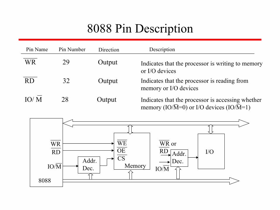
Pin Name Pin Number Direction Description

8088 Pin Description
Pin Name Pin Number Direction Description
READY 22 Input Informs the processor that the selected memory or I/O device is ready for a data transfer
8088 Selected memoryor I/O device
Data bus
READY READY
wait for memoryor I/O ready
Start data transfer

8088 Pin Description
Pin Name Pin Number Direction Description
HOLD 31 Input The execution of the processor is suspended as long as HOLD is high
HLDA 30 Output Acknowledges that the processor is suspended
8088
Memory
HOLD
HLDADevice 2
Bus
Procedure for Device 2 to use bus
Drive the HOLD signal of 8088 high
Wait for the HLDA signal of 8088 becoming high
Now, Device2 can send data to bus

8088 Pin DescriptionPin Name Pin Number Direction Description
NMI 17 Input Causes a non-maskable type-2 interrupt
INTR 18 Input Indicates a maskable interrupt request
INTA 24 Output Indicates that the processor has received anINTR request and is beginning interruptprocessing
NMI (non-maskable interrupt): a rising edge on NMI causes a type-2 interrupt
INTR: logic high on INTR poses an interrupt request. However, this request can be masked by IF (Interrupt enable Flag). The type of interrupt caused by INTR is read from data bus
8088 External device
Data bus
INTR
INTA
INTR
INTA
Data Bus Int. type
INTA: control when the interrupt type should be loaded onto the data bus

8088 Pin DescriptionPin Name Pin Number Direction Description
ALE 25 Output Indicates the current data on 8088 address/databus are address
D Q
G
8088
A[19:8]
ALE
AD[7:0]
D[7:0]
A[7:0]
A[19:8]
D latches
Buffer

8088 Pin Description
Pin Name Pin Number Direction Description
DEN 26 Output Disconnects data bus connection
DT / R 27 Output Indicates the direction of data transfer
8088
AD[7:0]
Data bus
D[7:0]
DEN
DT/R
DEN DT/ R
DEN DT/R
1 X Disconnected 0 0 To 8088 0 1 From 8088
8088 Pin Description
Pin Name Pin Number Direction Description
WR 29 Output Indicates that the processor is writing to memoryor I/O devices
RD 32 Output
IO/ M 28 Output
Indicates that the processor is reading from memory or I/O devices
Indicates that the processor is accessing whethermemory (IO/M=0) or I/O devices (IO/M=1)
WRRD
IO/M
8088
Memory
WEOECSAddr.
Dec.
Addr.Dec.
IO/M
WR orRD I/O

8088 Pin Description
Pin Name Pin Number Direction Description
AD[7:0] 9-16 I/O Address / Data bus
A[19:8] 2-8, 35-39 Input Address bus
LOCK 29 Input Lock output is used to lock peripherals off the system. Activated by using the LOCK: prefix on any instruction.

8284 Clock Generator
510
510
100K
10uF
+5V
Ready1Ready2
RES
RDY1RDY2
X1
X2
Ready
CLK
RESET RESET
CLK
Ready
8284 8088
Generates 33% duty cycle clock signal Generates RESET signal Synchronizes ready signals from memory and I/O devices
Basic functions: Clock generation. RESET synchronization. READY synchronization. Peripheral clock signal.
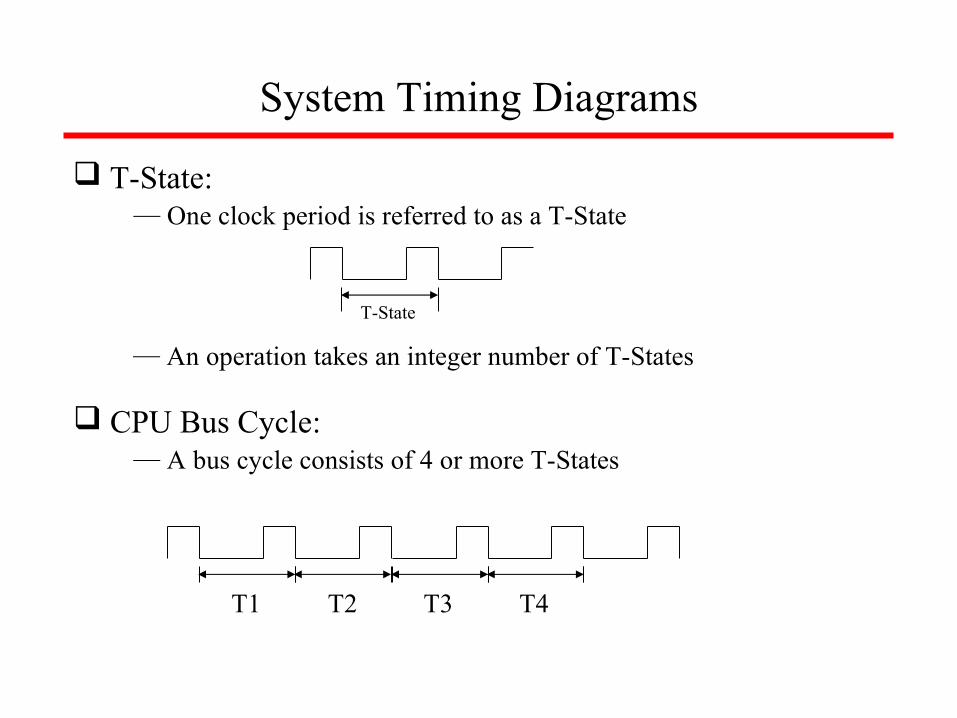
System Timing Diagrams
T-State:— One clock period is referred to as a T-State
T-State
— An operation takes an integer number of T-States
CPU Bus Cycle:— A bus cycle consists of 4 or more T-States
T1 T2 T3 T4

• Dump address on address bus. • Issue a read ( RD ) and set M/ IO to 1. • Wait for memory access cycle.
Memory Read Timing Diagrams

Memory Read Timing Diagrams
T1 T2 T3 T4
CLK
ALE
A[19:16] A[19:16] S3-S6
A[15:8] A[15:8]
AD[7:0] A[7:0] D[7:0]
IO/M
DT/R
DEN
RD
WR
A[15:8]
AD[7:0]
A[15:0]Buffer
D latch
Trans-ceiver
D[7:0]
DT/R
DEN
IO/M
WR
RD
8088
Memory

• Dump address on address bus. • Dump data on data bus. • Issue a write ( WR ) and set M/ IO to 1.
Memory Write Timing Diagrams

Memory Write Timing Diagrams
T1 T2 T3 T4
CLK
ALE
A[19:16] A[19:16] S3-S6
A[15:8] A[15:8]
AD[7:0] A[7:0] D[7:0]
IO/M
DT/R
DEN
RD
WR
A[15:8]
AD[7:0]
A[15:0]Buffer
D latch
Trans-ceiver
D[7:0]
DT/R
DEN
IO/M
WR
RD
8088
Memory

Bus TimingDuring T 1 : • The address is placed on the Address/Data bus. • Control signals M/ IO , ALE and DT/ R specify memory or I/O, latch the
address onto the address bus and set the direction of data transfer on data bus.
During T 2 : • 8086 issues the RD or WR signal, DEN , and, for a write, the data.
• DEN enables the memory or I/O device to receive the data for writes and the 8086 to receive the data for reads.
During T 3 : • This cycle is provided to allow memory to access data. • READY is sampled at the end of T 2 .
• If low, T 3 becomes a wait state. • Otherwise, the data bus is sampled at the end of T 3 .
During T 4 : • All bus signals are deactivated, in preparation for next bus cycle. • Data is sampled for reads, writes occur for writes.

Bus Timing
Timing: – Each BUS CYCLE on the 8086 equals four system clocking periods (T states). – The clock rate is 5MHz , therefore one Bus Cycle is 800ns . – The transfer rate is 1.25MHz .
Memory specs (memory access time) must match constraints of system timing. For example, bus timing for a read operation shows almost 600ns are needed to
read data. • However, memory must access faster due to setup times, e.g. Address setup and data
setup. • This subtracts off about 150ns . • Therefore, memory must access in at least 450ns minus another 30-40ns guard band for
buffers and decoders. • 420ns DRAM required for the 8086.

10.6 System Time Diagrams - CPU Bus CycleT2 T3 TW T4
Read Cycle(instruction fetch and memory operand read)
A8- A15
Address latches store the actual values
Memory Cycle (I/O cycle is similar but IO/M = 1)
S3- S6
Tri-state
A16 -A19
A0- A7
T1CLK
ALE
IO/M
A16 - A19
A8- A15
RD
AD0- AD7
DT/R
READY
DEN
Direction “READ” for the Data Buffer
Enables Data Buffer
WR
AD0- AD7
DT/R
Write Cycle (memory operand write)
A0- A7 D0- D7 (Data out)
DENDirection “READ” for the Data Buffer
Enables Data Buffer
Memory reads Data Bus
The slow device drives READY= 0the µ P samples READY
(if 0 a WAIT state follows)
D0- D7 (Data in)
µ P reads Data Bus

Interrupt Acknowledge Timing Diagrams
T1 T2 T3 T4
•••
•••
CLK
INTR
INTA
D[7:0] •••
8088 External device
Data bus
INTR
INTA
It takes one bus cycle to perform an interrupt acknowledge
During T1, the process tri-states the address bus
During T2, INTA is pulled low and remains low until it becomes inactive in T4
The interrupting devices places an 8-bit interrupt type during INTA is active
Int. Type

HOLD/HLDA Timing Diagrams
T2 T3 T4
•••
•••
CLK
HOLD
8088
Memory
HOLD
HLDADevice 2
BusHLDA
Hold State
The processor will examine HOLD signal at every rising clock edge
If HOLD=1, the processor will pull HLDA high at the end of T4 state (end of
the execution of the current instruction) and suspend its normal operation
If HOLD=0, the processor will pull down HLDA at the falling clock edge
and resume its normal operation

Memory Interface

11.3 Bus Buffering
8282
STB OE
D Q LE
Memory Address Decoder
Memory Chip 1
Memory Chip 2
Memory Chip n
Data Bus
Address Bus
8286
OE T
8282
STB OE
D Q LE
RDWR
IO/M
A16/S3-A19/S6
A8-A15
8088
AD0-AD7
ALE
DENDT/R
READY
74LS244
G1 G2
CE (Chip Enable) or CS (Chip Select), activate each chip
WR and RD for each chip
some high Address lines and IO/M
used to identify the accessed chip
the decoder drives READY: provides enough access time for the selected chip
some low address lines identify the internal accessed byte
(more for memory, few for I/O)
I/O Address Decoder
I/OChip 1
I/OChip 2
I/OChip m

Memory Chips
• The number of address pins is related to the number of memory locations . – Common sizes today are 1K to 256M locations. (10 and 28 address pins
are present.)• The data pins are typically bi-directional in read-write memories.
– The number of data pins is related to the size of the memory location . – For example, an 8-bit wide (byte-wide) memory device has 8 data pins. – Catalog listing of 1K X 8 indicate a byte addressable 8K memory.
• Each memory device has at least one chip select ( CS ) or chip enable ( CE ) or select ( S ) pin that enables the memory device.
• Each memory device has at least one control pin. – For ROMs, an output enable ( OE ) or gate ( G ) is present.
• The OE pin enables and disables a set of tristate buffers. – For RAMs, a read-write ( R/W ) or write enable ( WE ) and read enable
(OE ) are present. • For dual control pin devices, it must be hold true that both are not 0 at the
same time.

Memory Address Decoding
• The processor can usually address a memory space that is much larger than the memory space covered by an individual memory chip.
• In order to splice a memory device into the address space of the processor, decoding is necessary.
• For example, the 8088 issues 20-bit addresses for a total of 1MB of memory address space.
• However, the BIOS on a 2716 EPROM has only 2KB of memory and 11 address pins.
• A decoder can be used to decode the additional 9 address pins and allow the EPROM to be placed in any 2KB section of the 1MB address space.

Memory Address Decoding

A0-A13
16KBEPROM
chip OE
FFFFF
00000
Full address decoding
Memory Map -
M/IO18A19AM/IO18A19A1CS ⋅⋅=++=
WRRD
A19, A18 assigned to 00 => CS active for every address
from 00000 to 3FFFFA18 = 0A19 = 0
IO/M = 0IO/M = 0 => Memory map
A0...
A17256KBRAMchipA18
A19CS1’
MWTCMRDC
The same Memory-map assignment
CS1A18A19IO/M
A 7B 6C 5 74LS138 4
3E1 2E2 1E 0
A17A18A19
A14A15A16
A19 = 1, A18 = 0, A17 = 0activate the decoder
A16, A15, A14 select one EPROM chip
A14A15A16A17A18A19
CS2
A19=A18=...=A14=1 select the EPROM
All the address lines used by the decoder or memory chip => each byte is uniquely addressed = full address decoding
FFFFF
3FFFF
00000
FFFFFFC000
3FFFF
00000
FFFFFFC000
83FFF80000
3FFFF
00000
FFFFFFC000
9FFFF9C00083FFF80000
3FFFF
000008088 Memory Map
220 = 1,048,576 different
byte addresses = 1Mbyte
MRDC
A0...
A17
256KBRAMchip
WR RD
A 256Kbyte = 218 RAM chip has 18 address lines, A0 - A17
16KBEPROM
chip
16KBEPROM
chip
16KBEPROM
chip
16KBEPROM
chip
16KBEPROM
chip
16KBEPROM
chip
16KBEPROM
chipCS4CS5CS6CS7CS8CS9CS10
16KBEPROM
chip OECS3
A0-A13

Decoding Circuits

Memory Address Decoding
00000
FFFFF
30000
37FFF32KB 0 0 1 1 0 0 0 0 0 0 0 0 0 0 0 0 0 0 0 0
0 0 1 1 0 1 1 1 1 1 1 1 1 1 1 1 1 1 1 1
Addr[19:0]
These 5 address linesare not changed. They set the base address
These 15 address lines selectone of the 215 (32768) locationsinside the RAMs
Lowest address
Highest address
Addr[19]Addr[18]Addr[17]Addr[16]Addr[15]
IO/M
Addr[14:0]
CS
32KB
Using Full memory addressing space
Can we design a decoder such that the first address of the 32KB memory is 37124H?

Design a 1MB memory system consisting of multiple memory chips
Memory Address Decoding
— Solution 1:
256KB 256KB 256KB 256KB
Addr[17:0]
Addr[18]
Addr[19]
IO/M
CS
CS CS CS CS
2-to-4decoder

Design a 1MB memory system consisting of multiple memory chips
— Solution 2:
256KB 256KB 256KB 256KB
Addr[19:2]
Addr[1]
Addr[0]
IO/M
CS
CS CS CS CS
2-to-4decoder
Memory Address Decoding

Design a 1MB memory system consisting of multiple memory chips
Memory Address Decoding
— Solution 3:
256KB 256KB 256KB 256KB
Addr[19:18]
Addr[17]
Addr[6]
IO/M
CS
CS CS CS CS
2-to-4decoder
Addr[16:7]Addr[5:0]
It is a bad design, but still works!

Memory Address Decoding
Design a 1MB memory system consisting of multiple memory chips
— Solution 4:
256KB 256KB 512KB
CS CS CS
Addr[17:0]
Addr[18]Addr[19]
IO/MAddr[18]
Addr[19]IO/M
Addr[18]
Addr[19]
IO/M

Memory Address Decoding
Exercise Problem:
— A 64KB memory chip is used to build a memory system with the starting address of 7000H. A block of memory locations in the memory chip are damaged.
64KB0000H
3210H
3317H
FFFFH
Damaged block
70000H
73210H
73317H
7FFFFH
1M addressing space
73200H
733FFH
1M addressing space
Replace this block
Memory Address Decoding
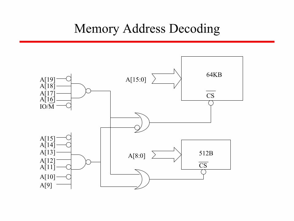
CS
CS
A[19]A[18]A[17]A[16]IO/M
A[15]A[14]A[13]A[12]A[11]
A[10]A[9]
64KB
512B
A[15:0]
A[8:0]

Memory Address Decoding
Exercise Problem:
— A 2MB memory chip with a damaged block (from 0DCF12H to 103745H) is used to build a 1MB memory system for an 8088-based computer
000000H
1FFFFFH
0FFFFFH
103745H
0DCF12H
Damaged block
000000H
1FFFFFH
18FFFFH
07FFFFH
512K
512K
Use these two
blocks
CS
A[20]
A[19:0]A[19:0]
A[19]

Memory Address Decoding
Partial decoding— Example:
build a 32KB memory system by using four 8KB memory chips The starting address of the 32KB memory system is 30000H
30000H
32000H
34000H
36000H
0 0 1 1 0 0 0 0 0 0 0 0 0 0 0 0 0 0 0 00 0 1 1 0 0 0 1 1 1 1 1 1 1 1 1 1 1 1 1
0 0 1 1 0 0 1 0 0 0 0 0 0 0 0 0 0 0 0 00 0 1 1 0 0 1 1 1 1 1 1 1 1 1 1 1 1 1 1
0 0 1 1 0 1 0 0 0 0 0 0 0 0 0 0 0 0 0 00 0 1 1 0 1 0 1 1 1 1 1 1 1 1 1 1 1 1 1
0 0 1 1 0 1 1 0 0 0 0 0 0 0 0 0 0 0 0 00 0 1 1 0 1 1 1 1 1 1 1 1 1 1 1 1 1 1 1
Chip #1
Chip #2
Chip #3
Chip #4
Low addr. of chip #1
high addr. of chip #1
Low addr. of chip #2
high addr. of chip #2
Low addr. of chip #3
high addr. of chip #3
Low addr. of chip #4
high addr. of chip #4

FFFFF
00000
Partial address decoding
Memory Map -
WRRD
A0...
A1564KBRAMchipA18
A19CS1’
MWTCMRDC
The same Memory-map assignment
CS1A18A19IO/M
Some address lines not used by the decoder or memory chip => mirror images = partial address decoding
FFFFF
3FFFF
00000
FFFFF
3FFFF300002FFFF200001FFFF100000FFFF00000
FFFFFFC000
7FFFF7C000
3FFFF300002FFFF200001FFFF100000FFFF00000
8088 Memory Map
A0...
A15
64KBRAMchip
WR RD
A 64Kbyte = 216 RAM chip has 16 address lines, A0 - A15
FFFFFFC000
9FFFF9C000
83FFF800007FFFF7C000
3FFFF300002FFFF200001FFFF100000FFFF00000
FFFFFFC000
DFFFFDC000
CF000CC000
9FFFF9C000
83FFF800007FFFF7C000
3FFFF300002FFFF200001FFFF100000FFFF00000
base image
base image
mirror images
MRDC
A0-A13
16KBEPROM
chip OE
A14A15A16A17A18
CS2
A18=...=A14=1 select the EPROM
mirror image
base image
mirror image
A19, A18 assigned to 00 => CS active for every address
from 00000 to 3FFFFA18 = 0A19 = 0
IO/M = 0IO/M = 0 => Memory map A16, A17 not used => four images for the same chip
16KBEPROM
chip
16KBEPROM
chip
16KBEPROM
chip
16KBEPROM
chip
16KBEPROM
chip
16KBEPROM
chip
16KBEPROM
chipCS4CS5CS6CS7CS8CS9CS10
16KBEPROM
chip OECS3
A0-A13
A 7B 6C 5 74LS138 4
3E1 2E2 1E 0
A17
A19
A14A15A16
A19 = 1, A17 = 0activate the decoder
A16, A15, A14 select one EPROM chip

Memory Address Decoding
— Implementation of partial decoding
Addr[12:0]
IO/M
CS
2-to-4decoder
Addr[13]
Addr[14]
CS CS CS
8KB 8KB 8KB 8KB
With the above decoding scheme, what happens if the processor accesses location 02117H, 32117H, and 9A117H? If two 16KB memory chips are used to implement the 32KB memory system, what is the partial decoding circuit? What are the advantage and disadvantage of partial decoding circuits?

Generating Wait States
Wait states are inserted into memory read or write cycles if slow memories are used in computer systemsReady signal is used to indicate if wait states are needed
8088
memory
data
Address
decoder Delaycircuit
Ready
QD QD
clk
Readyclr clr

1. Static RAM (SRAM)
• Essentially uses flip-flops to store charge (transistor circuit)
• As long as power is present, transistors do not lose charge (no refresh)
• Very fast (no sense circuitry to drive nor charge depletion)• Complex construction• Large bit circuit • Expensive• Used for Cache RAM because of speed and no need for
large volume

Static RAM Structure
six transistors per bit
(flip flop)
“NOT”
1
1
0
0 0/1 = example
01
0
1

Static RAM Operation
• Transistor arrangement (flip flop) has 2 stable logic states
• Write1.signal bit line: High 1 Low 0
2.address line active “switch” flip flop to stable state matching bit line
• Read1.address line active
2.drive bit line to same state as flip flop

2. Dynamic RAM (DRAM)
• Bits stored as charge in capacitors• Simpler construction• Smaller per bit• Less expensive• Slower than SRAM • Typical application is main memory• Essentially analogue -- level of charge
determines value

Dynamic RAM Structure
one transistor and one capacitor per bit
‘High’ Voltage at Y allows current to flow from X to Z or Z to XX
Y
Z
+

DRAM Operation
• Address line active
transistor switch closed and current flows• Write
1. data signal to bit line: High 1 Low 0
2. address line active transfers charge from bit line to capacitor
• Read1. address line active
2. transfer charge from capacitor to bit line (then to amplifier)
3. capacitor charge must be restored !

SRAM v.s. DRAM
Static Random Access Memory (SRAM)
Dynamic Random Access Memory (DRAM)
Storage element
Advantages1. Fast2. No refreshing operations
1. High density and less expensive
Disadvantages1. Large silicon area2. expensive
1. Slow2. Require refreshing operations
Applications High speed memory applications, Such as cache
Main memories in computer systems

Typical 16 Mb DRAM (4M x 4)
2 k x 2 k = 4 M
RAS = Row Addr. SelectCAS = Column Addr. Select
WE = Write EnableOE = Output Enable
nybble

Accessing DRAMs
DRAM block diagram
Addr[7:0]
CAS
RAS Storage Array
Column decoder
Row
deco der

Accessing DRAMs
Address bus selection circuit
QD QD
CLKset
QD
set setQ
decoderaddress
IO/M
RASCAS
To DRAMRow Address
Column Address
MUX

Accessing DRAMs
Refreshing operations
— Because leakage current will destroy information stored on DRAM capacitors
periodic refreshing operations are required for DRAM circuits
— During refreshing operation, DRAM circuit are not able to response processor’s
request to perform read or write operations
— How to suspend memory operations?
— DRAM controllers are developed to take care DRAM refreshing operations

I/O System Design

Overview of 8088 I/O System
65,536 possible I/O ports
Data transfer between ports and the processor is over data bus
8088 uses address bus A[15:0] to locate an I/O port
AL (or AX) is the processor register that takes input data (or provide output data)
I/O I/O I/O
Data bus
Address bus A[15:0]
AL
AX
8088

8088 Port Addressing Space
Addressing Space
FFFF
0000
00F8
00FF
Accessed directly byinstructions
Accessed throughDX
Accessing directly by instructions
IN AL, 80HIN AX, 6HOUT 3CH, ALOUT 0A0H, AX
Accessing through DX
IN AL, DXIN AX, DXOUT DX, ALOUT DX, AX

Input Port Implementation
8088
Data Bus
Address busDecoder
InputGating device
Other control signals
— The outputs of the gating device are high impedance when the processor is not accessing the input port
— When the processor is accessing the input port, the gating device transfers input data to CPU data bus
— The decoding circuit controls when the gating device has high impedance output and when it transfers input data to data bus

Input Port Implementation
Circuit Implementation
— Assume that the address of the input port is 9CH
Data bus Input dataTri-statebuffer
CE
RD IO/M
A7A6A5A4A3A2A1A0

Output Port Implementation
Circuit Implementation
— Assume that the address of the output port is 9CH
Data bus Output dataLatch
CLK
WR IO/M
A7A6A5A4A3A2A1A0

A Reconfigurable Port Decoder1 Vcc
A3A2
A1
A0
B3B2
B1
B0
A=B
A=B
A3A2
A1
A0
B3B2
B1
B0
A=B
A=B
A7
A6A5
A4
A3
A2A1
A0
R
RD or WR
IO/M

Direct I/O v.s. Memory-Mapped I/O
Memoryaddressingspace I/O
addressingspace
I/O
Memory addressingspace
00000
FFFFF
0000
FFFF
00000
FFFFF
Direct I/OMemory-mapped I/O
Direct I/O: I/O addresses are separated from memory address— Advantage: Do not take memory addressing space— Disadvantage: Use only AL or AX transferring data
Memory-mapped I/O: I/O ports are treated as memory locations— Advantage: Accessing I/O ports is like accessing memory locations Can use other instructions to access I/O ports— Disadvantage: Take memory addressing space

Handshaking• I/O devices are typically slower than the microprocessor. • Handshaking is used to synchronize I/O with the
microprocessor. – A device indicates that it is ready for a command or data (through
some I/O pin or port). – The processor issues a command to the device, and the device
indicates it is busy (not ready). – The I/O device finishes its task and indicates a ready condition,
and the cycle continues.
• There are two basic mechanisms for the processor to service a device. – Polling: Processor initiated. Device indicates it is ready by setting
some status bit and the processor periodically checks it.
– Interrupts: Device initiated. The act of setting a status bit causes an interrupt, and the processor calls an ISR to service the device.

8255 Programmable Peripheral Interface
Data bus
8088
D[7:0]
A0A1
RDWR
RESET
CS
Control port
PA[7:0]
PB[7:0]
PC[7:0]
A7A6A5A4A3A2
IO/MA1 A0 Port
0 00 11 01 1
PAPBPCControl
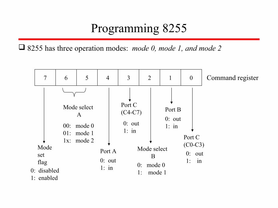
Programming 8255
8255 has three operation modes: mode 0, mode 1, and mode 2
7 6 5 4 3 2 1 0 Command register
Modesetflag
0: disabled1: enabled
Mode select A
00: mode 001: mode 11x: mode 2
Port A
0: out1: in
Port C(C4-C7)
0: out1: in
Mode select B
0: mode 01: mode 1
Port B
0: out1: in
Port C(C0-C3)
0: out1: in

Programming 8255
Mode 0:
— Ports A, B, and C can be individually programmed as input or output ports— Port C is divided into two 4-bit ports which are independent from each other
Mode 1:
— Ports A and B are programmed as input or output ports— Port C is used for handshaking
PA[7:0]
STBA
IBFA
INTRAPC3PC5PC4
PB[7:0]
STBB
IBFB
INTRBPC0PC1PC2
PC6, 7
8255
PA[7:0]
OBFA
ACKA
INTRAPC3PC6PC7
PB[7:0]
OBFB
ACKB
INTRBPC0PC1PC2
PC4, 5
8255


Programming 8255 Mode 2:
— Port A is programmed to be bi-directional— Port C is for handshaking— Port B can be either input or output in mode 0 or mode 1
PA[7:0]
OBFA
ACKA
INTRA
PC4
PC6PC7
STBA
IBFA
PC0
PC3PC58255
PC0
PC0
PB[7:0]
In Out In OutIn Out
Mode 0
STBB OBFB IBFB ACKB
INTRB INTRB
Mode 1
1. Can you design a decoder for an 8255 chip such that its base address is 40H?2. Write the instructions that set 8255 into mode 0, port A as input, port B as output,
PC0-PC3 as input, PC4-PC7 as output ?


Serial Data Transfer
Asynchronous v.s. Synchronous— Asynchronous transfer does not require clock signal. However, it transfers extra bits (start bits and stop bits) during data communication — Synchronous transfer does not transfer extra bits. However, it requires clock signal
Frame
Startbit B0 B1 B2 B3 B4 B5 B6
ParityStop bits
AsynchronousData transfer
SynchronousData transfer
clk
data
B0 B1 B2 B3 B4 B5
data
Baud (Baud is # of bits transmitted/sec, including start, stop, data and parity).

8251 USART Interface
A7A6A5A4A3A2A1
IO/M
D[7:0]
RD RD
WR WRA0 C/D
CLK CLKTxC
RxC
TxD
RxD
8251 RS232

Programming 8251
8251 mode register
7 6 5 4 3 2 1 0 Mode register
Number of Stop bits
00: invalid01: 1 bit10: 1.5 bits11: 2 bits
Parity0: odd1: even
Parity enable0: disable1: enable
Character length
00: 5 bits01: 6 bits10: 7 bits11: 8 bits
Baud Rate
00: Syn. Mode01: x1 clock10: x16 clock11: x64 clock

Programming 8251
8251 command register
EH IR RTS ER SBRK RxE DTR TxE command register
TxE: transmit enableDTR: data terminal readyRxE: receiver enableSBPRK: send break characterER: error resetRTS: request to sendIR: internal resetEH: enter hunt mode

Programming 8251
8251 status register
DSR SYNDET FE OE PE TxEMPTY RxRDY TxRDY status register
TxRDY: transmit readyRxRDY: receiver readyTxEMPTY: transmitter emptyPE: parity errorOE: overrun errorFE: framing errorSYNDET: sync. character detectedDSR: data set ready

Simple Serial I/O Procedures
Read
start
Check RxRDY
Is it logic 1?
Read data register*
end
Yes
No
* This clears RxRDY
Write
start
Check TxRDY
Is it logic 1?
Write data register*
end
Yes
No
* This clears TxRDY
Errors
– Parity error: Received data has wrong error -- transmission bit flip due to noise.
– Framing error: Start and stop bits not in their proper places.
• This usually results if the receiver is receiving data at the incorrect baud rate.
– Overrun error: Data has overrun the internal receiver FIFO buffer.
• Software is failing to read the data from the FIFO.

Programmable Timer 8254

8254 Programming

8254 Programming
• Each counter may be programmed with a count of 1 to FFFFH. – Minimum count is 1 all modes except 2 and 3 with
minimum count of 2.
• Each counter has a program control word used to select the way the counter operates. – If two bytes are programmed, then the first byte (LSB)
stops the count, and the second byte (MSB) starts the counter with the new count.

8254 Modes
• Mode 0: An events counter enabled with G. – The output becomes a logic 0 when the control word is written and
remains there until N plus the number of programmed counts.
Mode 1: One-shot mode. – The G input triggers the counter to output a 0 pulse for `count' clocks. – Counter reloaded if G is pulsed again.

8254 Modes
• Mode 2: Counter generates a series of pulses 1 clock pulse wide. – The seperation between pulses is determined by the count. – The cycle is repeated until reprogrammed or G pin set to 0.
– Mode 3: Generates a continuous square-wave with G set to 1. • If count is even, 50% duty cycle otherwise OUT is high 1 cycle longer.

8254 Modes