Embed Size (px)
Citation preview

1
Introduction to Biomedical Engineering
Kung-Bin Sung
Device/Instrumentation III

2
Outline• Chapter 8 and chapter 5 of 1st edition:
Bioinstrumentation– Review of signals and system, analog
circuits– Operational amplifiers, instrumentation
amplifiers– Transfer function, frequency response– Filters– Non-ideal characteristics of op-amps– Noise and interference– Data acquisition (sampling, digitization)

3
Types of medical instrumentation
• Biopotential• Blood (pressure, flow, volume, etc)• Respiratory (pressure, flow rate, lung
volume, gas concentration)• Chemical (gas, electrolytes, metabolites)• Therapeutic and prosthetic devices• Imaging (X-ray, CT, ultrasound, MRI,
PET, etc.)• Others

4
Overview of bioinstrumentation
Emphasis of this module will be on instruments that measure or monitor physiological activities/functions
Basic instrumentation system

5
Characteristics of bio-signals
EOG (ElectroOculoGram): measures the resting potential of retinaERG (ElectroRetinoGram): measures the electrical response of retina to light stimuli
EGG (electrogastrogram): measures muscular activity of the stomach

6
Signal amplification
• Gain up to 107
• Cascade (series) of amplifiers, with gain of 10-10000 each
• DC offset must be removed (ex. by HPF with a cutoff frequency of 1Hz)
• Further reduction of the common-mode signal

7
Time-varying signals
)2cos()cos()( 111 θπθω +=+= ftVtVtv
θθ ∠== 111 VeVV j θθθ sincos je j +=
Sinusoidal signals have amplitude, frequency and phase
IZV ˆ1 = RZR =
2/πωω jL LeLjZ ==
2/11 π
ωωj
C eCCj
Z −==
Phasors: complex numbers (magnitude and phase angle) representing the sinusoidal signal (without the frequency)
Since capacitors and inductors introduce phase shift to the signal, their impedances Z can be expressed in phasors as following

8
Laplace transform
∫∞ −==0
)()()( dtetfsFtfL st
Definition
Some properties of Laplace transform

9
Laplace domain analysis
ωjs = RZR =
sLZL =
sCZC
1=
Use Laplace transform to describe time-varying signals ⇒Differential equations become algebraic equations
Let
Inverse Laplace transform is used when we want to obtain the time-domain signals (ex. transient response of circuits)
10
Laplace transform pairs
11
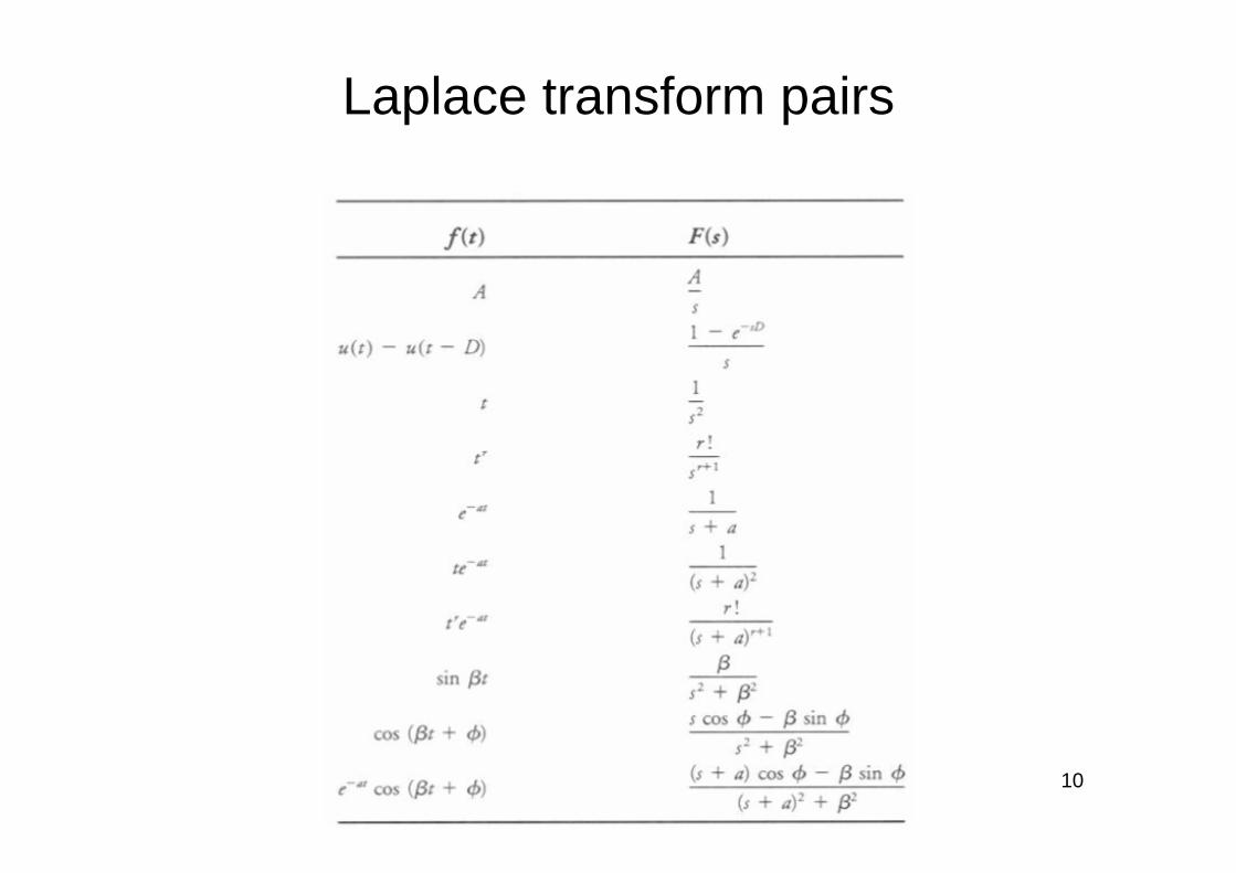
Analog circuitsWheatstone bridge circuit
)()(321
12
x
xssRxRab RR
RVRR
RVVVV+
−+
=−=
The measured Vab can be used to get R, which represents unknown resistance of devices such a strain gauge and a thermistor

12
Operational amplifier (op-amp)
)( npout vvAV −=
A ~ 106
For ideal op-amps: - No current flows into or out of input terminals (input impedance = infinity)- vp = vn since A ~ 106
- Output impedance = 0
Open-loop voltage gain
Cautions for op-amp circuitsOp-amps are used with (negative) feedback loops for stabilityMust be in the active region (input and output not saturated)

13
Op-amp circuitsVoltage follower or unity buffer
Vout = Vin
G=1
Advantage: input current is ~0, high input impedance. Output current drawn from the op-amp can drive a load (ZL) or next stage of circuit; particularly suitable as the first stage for physiological measurements
14
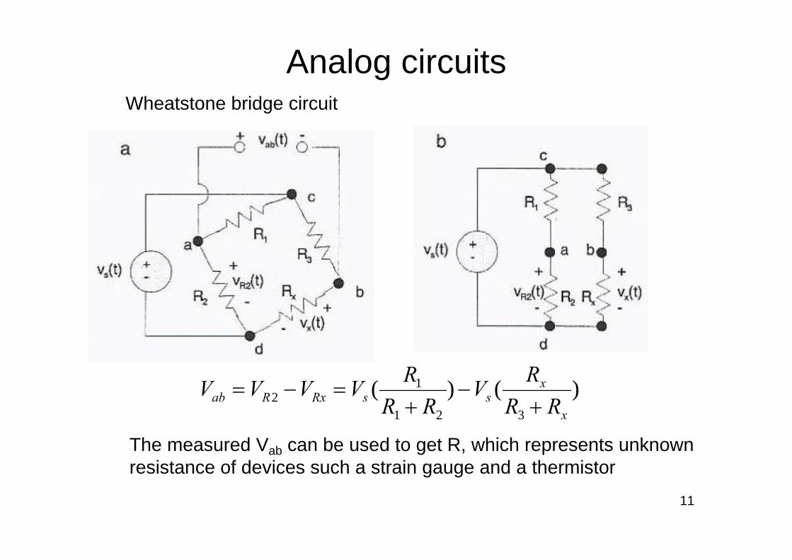
Op-amp circuits
21
2122 RRvRiRiv in
out −=−=−=
1
2
RRG −=
Input impedance = R1
Inverting amplifier Non-inverting amplifier
21
RRvvv in
inout +=
1
21RRG +=
Input impedance =Zin of the op-amp

15
Op-amp circuits
)(2
2
1
1
RV
RVRRiv fffout +−==
)( 22
11
VRR
VRR
G ff +−=
Summing amplifier
You can add more input voltages…
Vout = −(V1+V2+V3)

16
Op-amp circuits
243
4
1
211
1
2 VRR
RRRRV
RRVout ⎟⎟
⎠
⎞⎜⎜⎝
⎛+⎟⎟
⎠
⎞⎜⎜⎝
⎛ ++−=
( )121
2 VVRRVout −=
Subtractor
If R1=R3, R2=R4
This is called a differential amplifier
If a differential signal (ex. biopotential) is measured across the input terminals
1
2
12 RR
VVVG out
d =−
=Differential gain
17
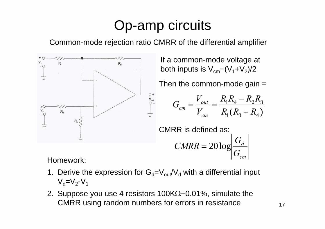
Op-amp circuits
)( 431
3241
RRRRRRR
VVGcm
outcm +
−==
Then the common-mode gain =
Homework: 1. Derive the expression for Gd=Vout/Vd with a differential input
Vd=V2-V1
2. Suppose you use 4 resistors 100KΩ±0.01%, simulate the CMRR using random numbers for errors in resistance
Common-mode rejection ratio CMRR of the differential amplifier
If a common-mode voltage at both inputs is Vcm=(V1+V2)/2
cm
d
GGCMRR log20=
CMRR is defined as:

18
More on differential amplifier
Vout = V2-V1
• For measuring biopotentials, voltage gain can be obtained by subsequent amplifier stages• Input impedance is small ~R• In ECG, the impedance of skin is ~MΩ(can be lowered by applying electrolyte gel to 15-100KΩ)• Mismatches in R reduce the CMRR
Add unity buffers in the inputs

19
Instrumentation amplifier
( )2143
2VV
RRR
VVgain
gain −+
=−
gaind R
RG 21+=
43 VVVout −=
In practice, Rgain is external and used to select gain which is typically 1-1000

20
Instrumentation amplifier
1=cmG
1=dGgain
d RRG 21+=
0≈cmG
Provides good CMRR without the need for precisely matching resistors

21
Example of common-mode voltageInterference from power line (60Hz) can induce current idb
Gdbcm Ziv ⋅=
For idb = 0.2 µAZG = 50 kΩ
vcm = 10 mV

22
Driven-right-leg circuitOutput is connected to the right leg through a surface electrode, which provides negative feedback

23
Driven-right-leg circuit
Current at inverting input:

24
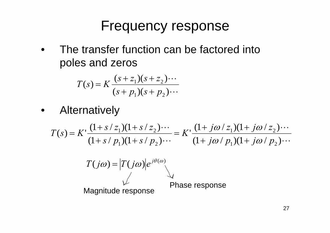
Transfer function• Relationship between the input and output
• Since T(s) also provides information on the frequency and phase of the instrument –frequency response
)()()(sVsVsT
in
out=
fjjs πω 2==
T(s)Vin(s) Vout(s)

25
Transfer function – example
1
11
11
11)(sCCsR
sCRsZi
+=+=
)1)(1()()(
)(2211
12
CsRCsRCsR
sZsZ
sTi
f
++=−=
22
2
22
111)(
CsRR
sCR
sZ f +=
+=

26
Transfer function – example2
1)(
)()()( 111
211 +=
+= CsR
sZsZsZsT
))(1()()()( 221121 CsRCsRsTsTsT +−==
222 )()(
)( CsRsZsZ
sTi
f −=−=
27
Frequency response• The transfer function can be factored into
poles and zeros
• Alternatively
⋅⋅⋅++⋅⋅⋅++
=))(())(()(
21
21
pspszszsKsT
⋅⋅⋅++⋅⋅⋅++
=⋅⋅⋅++⋅⋅⋅++
=)/1)(/1()/1)(/1('
)/1)(/1()/1)(/1(')(
21
21
21
21
pjpjzjzjK
pspszszsKsT
ωωωω
)()()( ωθωω jejTjT =
Phase responseMagnitude response
28
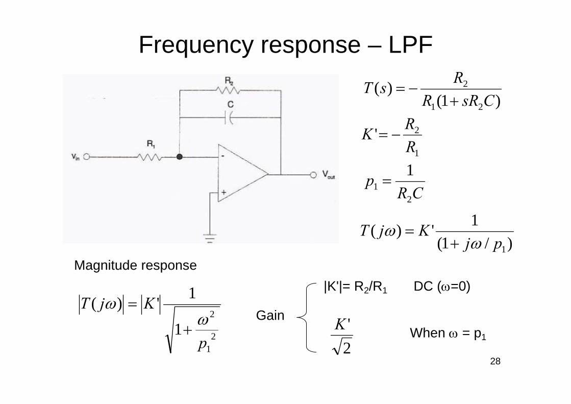
Frequency response – LPF
)1()(
21
2
CsRRRsT+
−=
1
2'RRK −=
CRp
21
1=
)/1(1')(
1pjKjT
ωω
+=
21
2
1
1')(
p
KjTω
ω+
=
Magnitude response|K'|= R2/R1 DC (ω=0)
Gain
2'K When ω = p1

29
Frequency response– LPF
CRfc
221
π=∴
2)(
)2( maxω
πjT
fjT c =
Cut-off frequency fc: the magnitude response is
In this example
12 pfcc == πω
(-3dB power attenuation)

30
Frequency response – HPF
CsRCsRsT1
2
1)(
+−=
1
2
/1)(
pjCRjjT
ωωω
+−=
CRp
11
1=
221
2
2
1)(
CR
CRjTω
ωω+
=0 DC (ω=0)
Gain
1
2
RR
− When ω → ∞
CRfc
121π
=∴12 pfcc == πω

31
Frequency response – HPF, BPF
Homework: • For the circuit on slide 25, find out the cut-off frequencies corresponding to ω1 and ω2, respectively• What modifications can you do to make a band-stop filter?
High pass filter Band pass filter Band stop filter
32
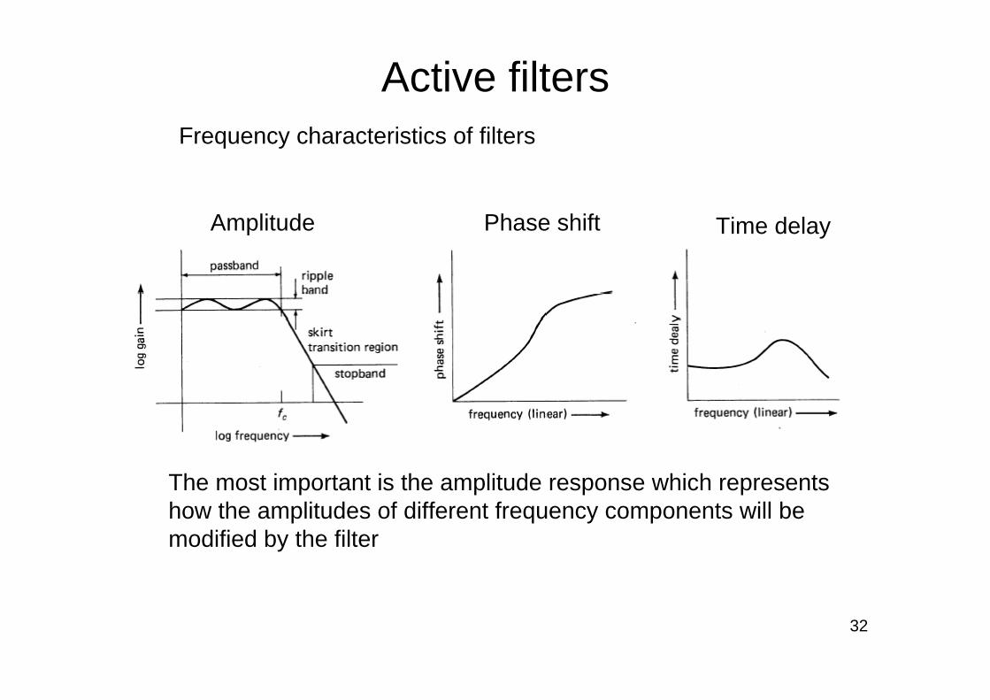
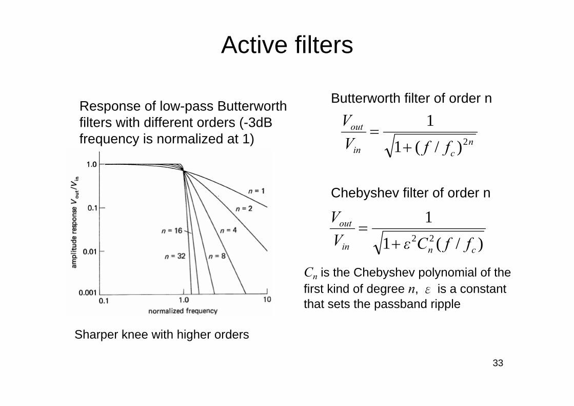
Active filtersFrequency characteristics of filters
Amplitude Phase shift Time delay
The most important is the amplitude response which represents how the amplitudes of different frequency components will be modified by the filter
33
Active filters
)/(1122
cnin
out
ffCεVV
+=
ncin
out
ffVV
2)/(11
+=
Response of low-pass Butterworth filters with different orders (-3dB frequency is normalized at 1)
Butterworth filter of order n
Chebyshev filter of order n
Cn is the Chebyshev polynomial of the first kind of degree n, ε is a constant that sets the passband ripple
Sharper knee with higher orders

34
Active filtersComparison of several 6-pole low-pass filters
Step response (-3dB at 1Hz)

35
Active filter circuits – VCVS
Low-passHigh-pass

36
VCVS filter design
cfRC
π21
=
cn ffRC
π21
=
- Each circuit is a 2-pole filter; i.e. for an n-pole filter, you need to cascade n/2 VCVS sections- Within each section, set R1=R2=R and C1=C2=C- Set the gain K according to the table- For Butterworth filters
nc ffRC
/21
π=
fc is the -3dB frequency
- For Bessel and Chebyshew low-pass filters
- For Bessel and Chebyshew high-pass filters

37
Non-ideal op-ampInput bias current IB: simply the base or gate currents of the input transistors (could be current source or sink) – the effect of IB can be reduced by selecting resistors to equalize the effective impedance to ground from the two inputs

38
Non-ideal op-ampInput offset current IOS: difference in input currents between two inputs; typically 0.1~0.5 IB
Input offset voltage: the difference in input voltages necessary to bring the output to zero (due to imperfectly balanced input stages)
The offset voltage can be eliminated by adjusting null offset pots on some op-amps (with inputs connecting to ground through resistors)

39
Non-ideal op-amp cont.Voltage gain: typically 105-106 at dc and drops to 1 at some fT (~ 1-10 MHz); when used with feedback (closed-loop gain = G), the bandwidth of the circuit will be fT/G
Output current: due to limited output current capability, the max. output voltage range (swing) of op-amp is reduced at small load resistances

40
Practical considerations• Negative feedback (resistor between the
output and the inverted input terminal) provides a linear input/output response and in general stability of the circuit
• Choose resistor values 1kΩ-1MΩ (best 10kΩ–100kΩ)
• Match input impedances of the two inputs to improve CMRR
• Equalize the effective resistance to ground at the two input terminals to minimize the effects of IB

41
Matching effective impedance to ground
The voltage gain is 5 for both circuits
40KΩ∥10KΩ = 8KΩ
So the effective impedance to ground from both input terminals is the same

42
Noise• Interference from outside sources
– Power lines, radio/TV/RF signals– Can be reduced by filtering, careful wiring and
shielding• Noise inherent to the circuit
– Random processes– Can be reduced by good circuit design practice,
but not completely eliminated
)(
)(log20rmsn
rmss
VV
SNR =
Signal-to-noise ratio2/1
0
2 )(1⎥⎦⎤
⎢⎣⎡= ∫
T
rms dttvT
VdB

43
Noise
• Types of fundamental (inherent) noise:– Thermal noise (Johnson noise or white
noise)– Shot noise– Flicker (1/f) noise– Transducer limitations

44
Noise
kTRBrmsVnoise 4)( =k: Boltzmann’s constantT: absolute temperature (°K)R: resistance (Ω)B: bandwidth fmax-fmin
Thermal noise: generated in a resistor due to thermal motion of atoms/molecules
Thermal noise contains superposition of all frequencies ⇒ white noise
nnnNS ==/
Shot noise: arises from the statistical uncertainty of counting discrete events
Flicker (1/f) noise: power spectrum is ~1/f; somewhat mysterious; found related to resistive materials of resistors and their connections
Shot noise =dn/dt is the count rate∆t is the time interval for the measurement
ntdtdn
≈∆

45
InterferenceElectric fields existing in power lines can couple into instruments and human body (capacitors)
46
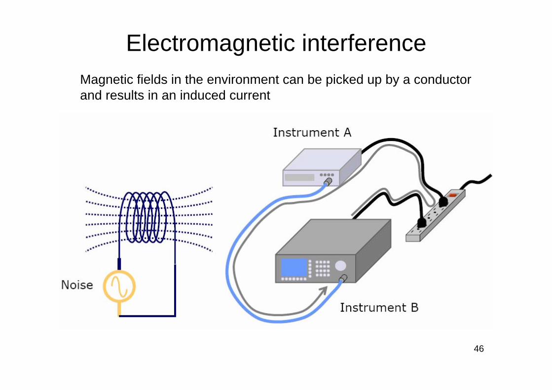
Electromagnetic interferenceMagnetic fields in the environment can be picked up by a conductor and results in an induced current

47
Electromagnetic interference
Reduce induced current by minimizing the area formed by the closed loop (twisting the lead wires and locating close to the body)
Time-varying magnetic field induces a current in a closed loop

48
A/D conversionConversion of Analog signal to Digital (integer) numbers
Continuous (analog) valuesDiscrete (digital)
numbers
Continuous time → discrete time interval ∆T
∴ A/D conversion is a process to1. “Sample” a real world signal at finite time intervals2. Represent the sampled signal with finite number of values
∆T

49
Sampling rate (frequency)How fast do we need to sample? First define the sampling frequency:
Tfsampling ∆
=1
max2 ffsampling >
(sample/s)
Intuitively, we must sample fast enough to avoid distortion of the signal or loss of information ⇒ easier to explain in the frequency domain
where fmax is the highest frequency present in the analog signal
(sampling theorem)
What happens if the above criterion is not met?- Loss of high frequency information in the signal- Even worse, the data after sampling may contain false information about the original signal ⇒ frequency aliasing
50
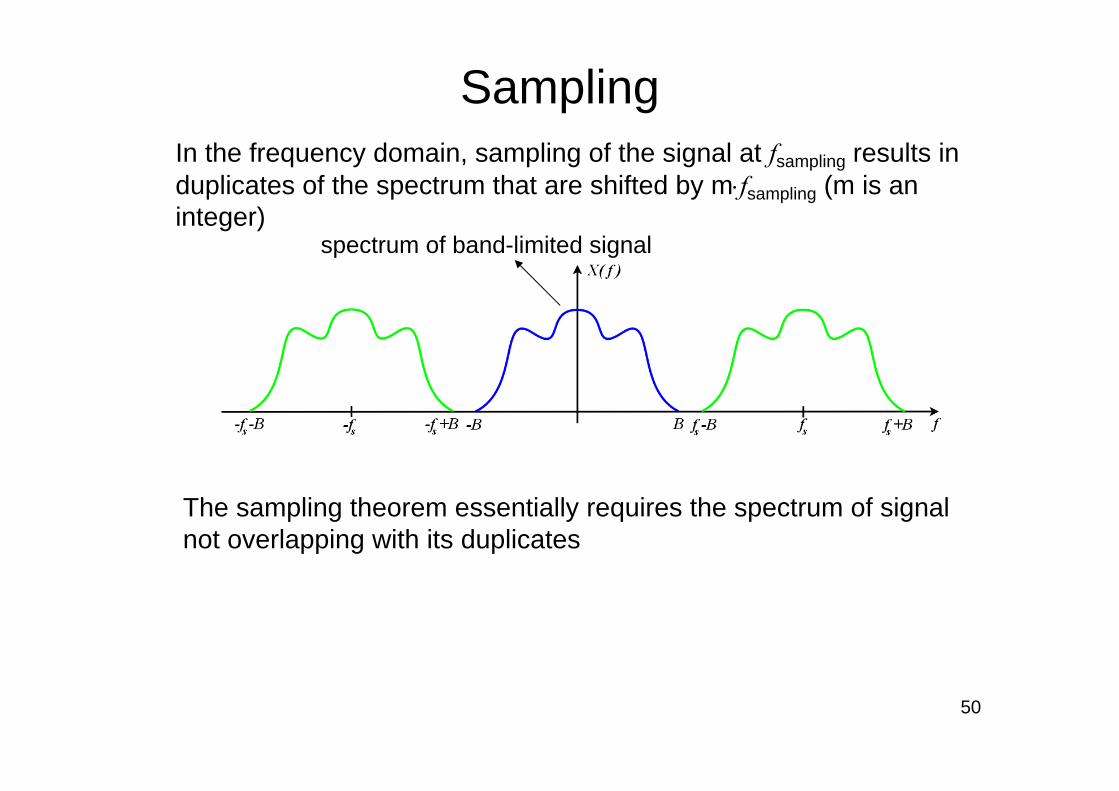
SamplingIn the frequency domain, sampling of the signal at fsampling results in duplicates of the spectrum that are shifted by m⋅fsampling (m is an integer)
spectrum of band-limited signal
The sampling theorem essentially requires the spectrum of signalnot overlapping with its duplicates

51
Frequency aliasingWhen the sampling theorem condition is not satisfied
Bffsampling 22 max =<
The high-frequency region overlaps and shape of spectrum is changed (summed). The process is not reversible ⇒ information is lost

52
Anti-aliasing- In the real world, no signal is strictly band-limited. But an effective bandwidth can be defined and used to find the sampling frequency- To avoid frequency aliasing, a low-pass filter is applied to the signal prior to sampling
X(f)
Low pass filter cutoff at B
Bfsampling 2>
53
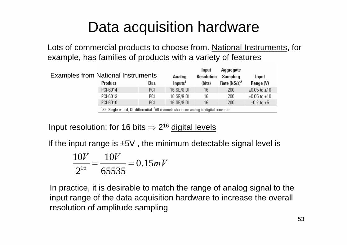
Data acquisition hardwareLots of commercial products to choose from. National Instruments, for example, has families of products with a variety of features
Input resolution: for 16 bits ⇒ 216 digital levels
If the input range is ±5V , the minimum detectable signal level is
mVVV 15.06553510
210
16 ==
In practice, it is desirable to match the range of analog signal to the input range of the data acquisition hardware to increase the overall resolution of amplitude sampling
Examples from National Instruments
54
References
• The Art of Electronics (2nd ed.), by Paul Horowitz and Winfield Hill
– Ch5: Active filters– Ch7
• Medical Instrumentation: application and design, 3rd ed., edited by John G. Webster
– Ch3: Amplifiers and Signal Processing