Embed Size (px)
Citation preview
Introduction to Data Conversion
EE174 – SJSULecture #2Tan Nguyen
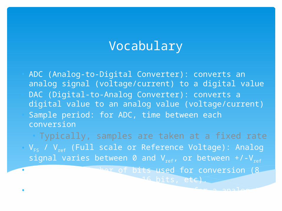
Vocabulary
• ADC (Analog-to-Digital Converter): converts an analog signal (voltage/current) to a digital value
• DAC (Digital-to-Analog Converter): converts a digital value to an analog value (voltage/current)
• Sample period: for ADC, time between each conversion
• Typically, samples are taken at a fixed rate• VFS / Vref (Full scale or Reference Voltage): Analog signal
varies between 0 and Vref, or between +/-Vref
• Resolution: Number of bits used for conversion (8 bits, 10 bits, 12 bits, 16 bits, etc).
• Conversion Time: The time it takes for a analog-to-digital conversion
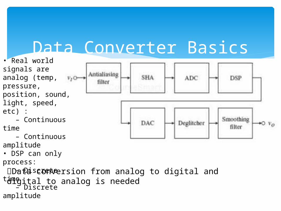
Data Converter Basics• Real world signals are analog (temp, pressure, position, sound, light, speed, etc) : – Continuous time – Continuous amplitude• DSP can only process: – Discrete time – Discrete amplitudeData conversion from analog to digital and digital to analog is needed
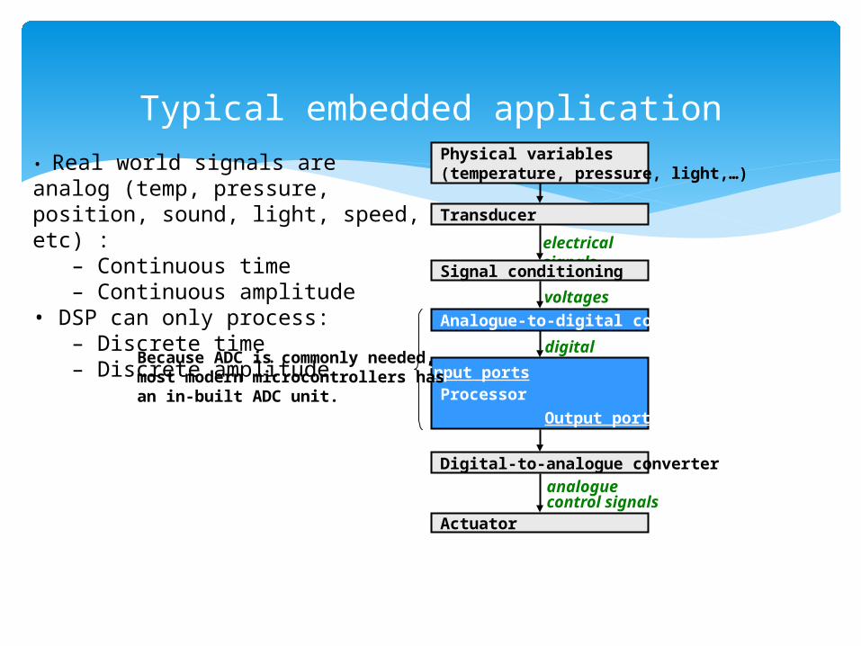
Typical embedded applicationPhysical variables(temperature, pressure, light,…)
Transducer
electrical signals
Analogue-to-digital converter
digital signals
Digital-to-analogue converter
Actuator
analogue control signals
Signal conditioning
voltages
ProcessorInput ports
Output ports
Because ADC is commonly needed,most modern microcontrollers has an in-built ADC unit.
• Real world signals are analog (temp, pressure, position, sound, light, speed, etc) : – Continuous time – Continuous amplitude• DSP can only process: – Discrete time – Discrete amplitude
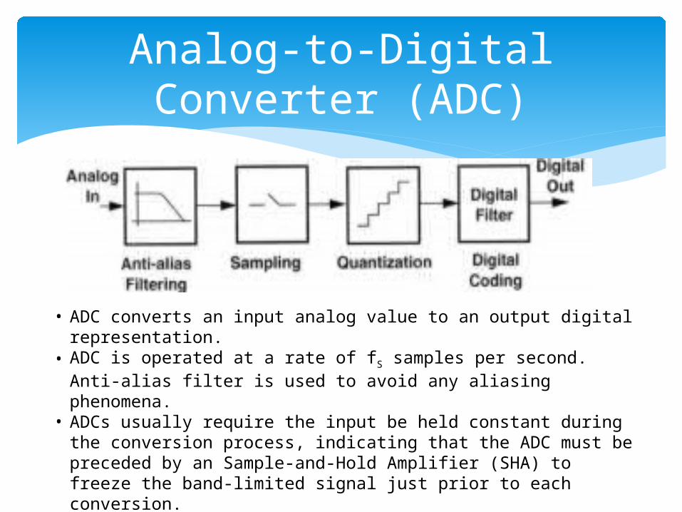
Analog-to-Digital Converter (ADC)
• ADC converts an input analog value to an output digital representation.
• ADC is operated at a rate of fS samples per second. Anti-alias filter is used to avoid any aliasing phenomena.
• ADCs usually require the input be held constant during the conversion process, indicating that the ADC must be preceded by an Sample-and-Hold Amplifier (SHA) to freeze the band-limited signal just prior to each conversion.
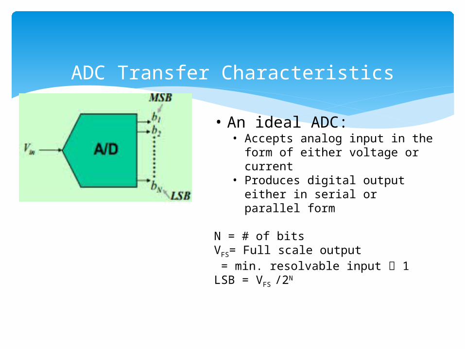
ADC Transfer Characteristics
• An ideal ADC:• Accepts analog input in the
form of either voltage or current • Produces digital output either in
serial or parallel form
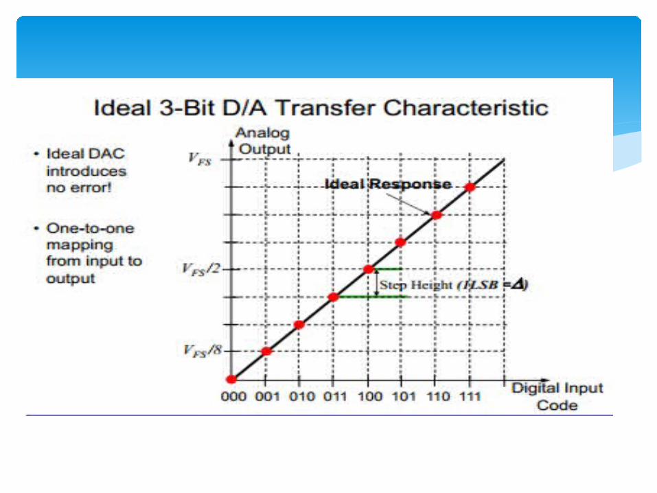
N = # of bitsVFS= Full scale output = min. resolvable input 1 LSB = VFS /2N
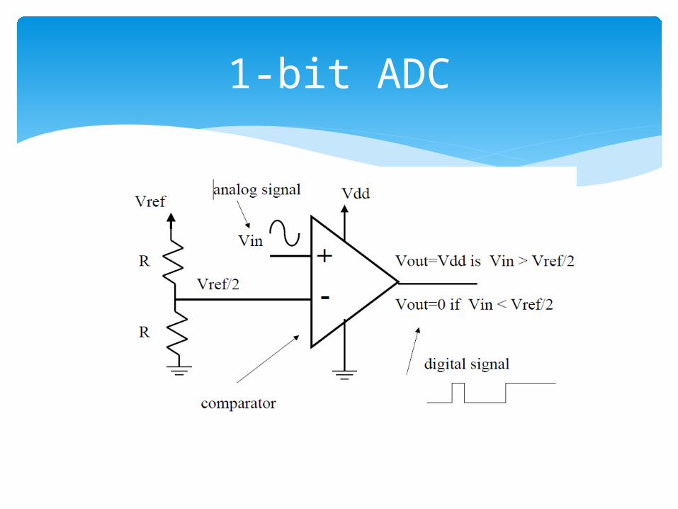
1-bit ADC
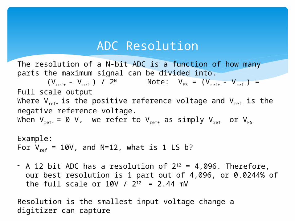
ADC ResolutionThe resolution of a N-bit ADC is a function of how many parts the maximum signal can be divided into.
(Vref+ - Vref-) / 2N Note: VFS = (Vref+ - Vref-) = Full scale outputWhere Vref+ is the positive reference voltage and Vref- is the negative reference voltage.When Vref- = 0 V, we refer to Vref+ as simply Vref or VFS
Example: For Vref = 10V, and N=12, what is 1 LS b?
- A 12 bit ADC has a resolution of 212 = 4,096. Therefore, our best resolution is 1 part out of 4,096, or 0.0244% of the full scale or 10V / 212 = 2.44 mV
Resolution is the smallest input voltage change a digitizer can capture
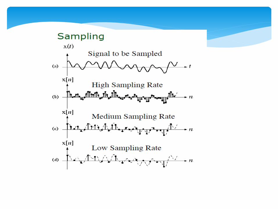
ADC : The process There are two related steps in A-to-D conversion:
Sampling Quantization
Sampling:
The analogue signal is extracted, usually at regularly spaced time instants.
The samples have real values.
Quantization:
The samples are quantized to discrete levels.
Each sample is represented as a digital value.
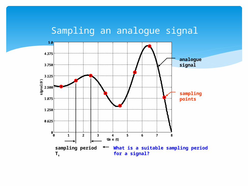
Sampling an analogue signal
0 1 2 3 4 5 6 7 80
0.625
1.250
1.875
2.500
3.125
3.750
4.375
5.0
time (t)
sig
na
l (V
)
analogue signal
samplingpoints
sampling period Ts
What is a suitable sampling period for a signal?
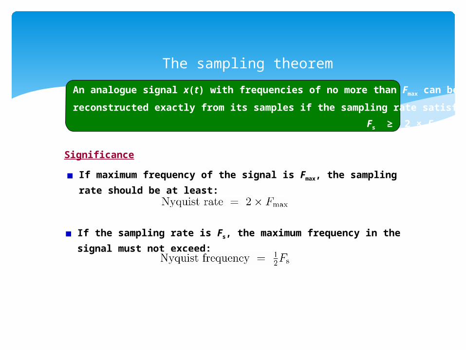
The sampling theorem
An analogue signal x(t) with frequencies of no more than Fmax can be
reconstructed exactly from its samples if the sampling rate satisfies:
Fs ≥ 2 × Fmax.
Significance
If maximum frequency of the signal is Fmax, the sampling
rate should be at least:
If the sampling rate is Fs, the maximum frequency in the
signal must not exceed:
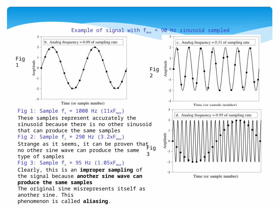
Fig 1
Fig 2
Fig 3
Fig 1: Sample fs = 1000 Hz (11xFmax)These samples represent accurately the sinusoid because there is no other sinusoid that can produce the same samples Fig 2: Sample fs = 290 Hz (3.2xFmax)Strange as it seems, it can be proven that no other sine wave can produce the same type of samplesFig 3: Sample fs = 95 Hz (1.05xFmax)Clearly, this is an improper sampling of the signal because another sine wave can produce the same samplesThe original sine misrepresents itself as another sine. Thisphenomenon is called aliasing.
Example of signal with fmax = 90 Hz sinusoid sampled
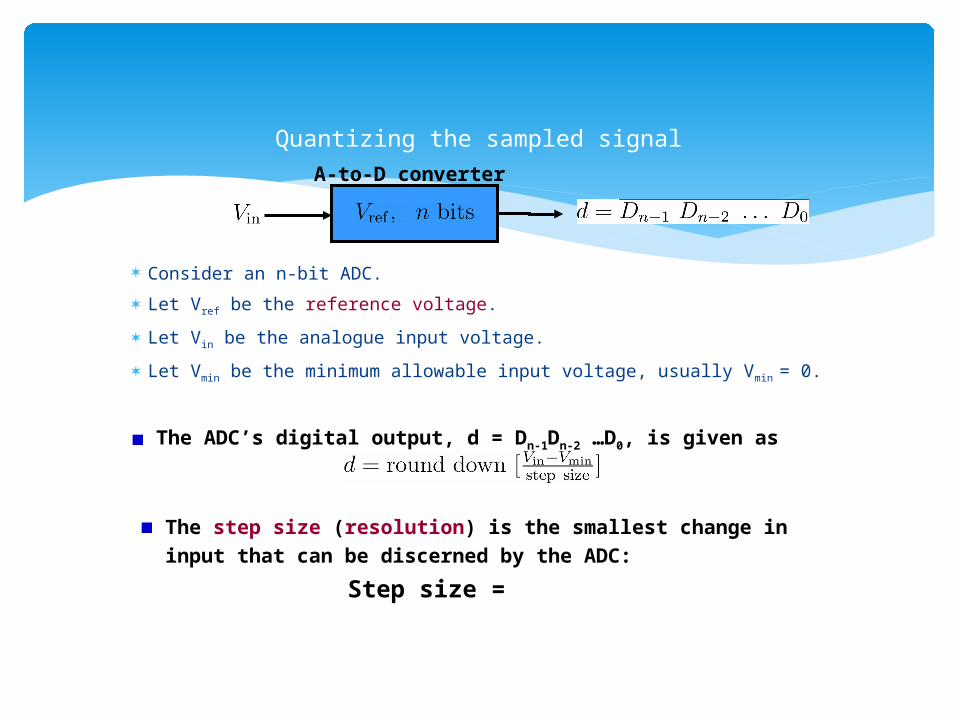
Quantizing the sampled signal
Consider an n-bit ADC.
Let Vref be the reference voltage.
Let Vin be the analogue input voltage.
Let Vmin be the minimum allowable input voltage, usually Vmin = 0.
A-to-D converter
The ADC’s digital output, d = Dn-1Dn-2 …D0, is given as
The step size (resolution) is the smallest change in input that can be discerned by the ADC:
Step size =
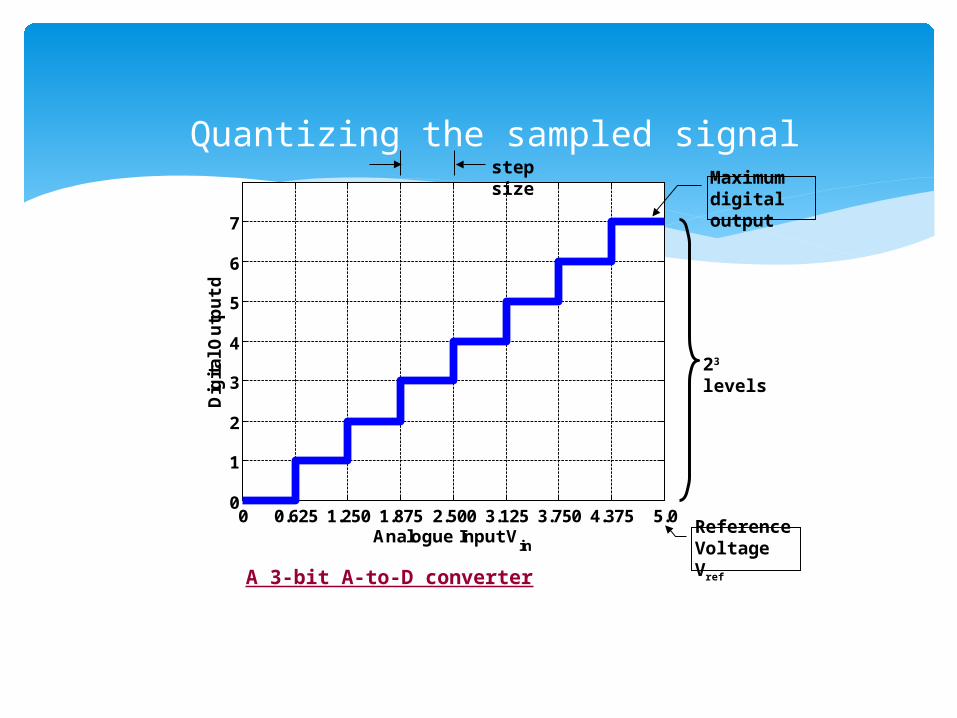
0 0.625 1.250 1.875 2.500 3.125 3.750 4.375 5.00
1
2
3
4
5
6
7
Analogue Input Vin
Dig
ita
l O
utp
ut
d
Quantizing the sampled signalMaximum digital output
step size
23 levels
A 3-bit A-to-D converter
ReferenceVoltage Vref
0 1 2 3 4 5 6 7 80
0.625
1.250
1.875
2.500
3.125
3.750
4.375
5.0
time (t)
sig
na
l (V
)
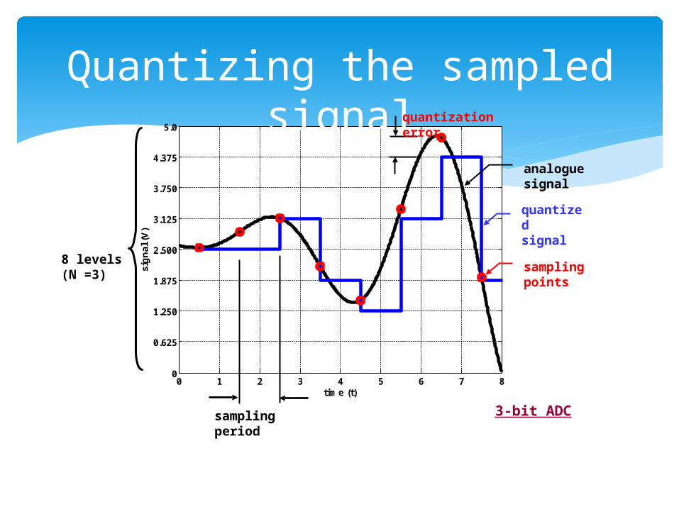
Quantizing the sampled signal
analogue signal
samplingpoints
sampling period
quantization error
quantizedsignal
8 levels(N =3)
3-bit ADC
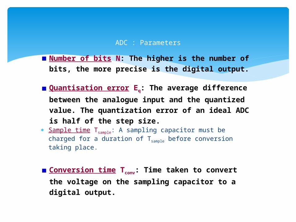
ADC : Parameters
Sample time Tsample: A sampling capacitor must be charged for a duration of Tsample before conversion taking place.
Conversion time Tconv: Time taken to convert
the voltage on the sampling capacitor to a digital output.
Quantisation error Eq: The average difference
between the analogue input and the quantized value. The quantization error of an ideal ADC is half of the step size.
Number of bits N: The higher is the number of bits, the more precise is the digital output.
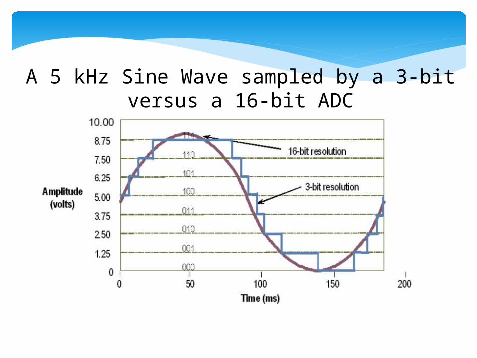
A 5 kHz Sine Wave sampled by a 3-bit versus a 16-bit ADC
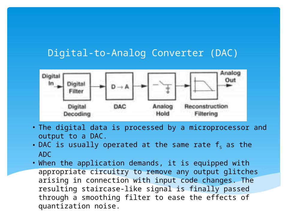
Digital-to-Analog Converter (DAC)
• The digital data is processed by a microprocessor and output to a DAC.
• DAC is usually operated at the same rate fS as the ADC• When the application demands, it is equipped with appropriate
circuitry to remove any output glitches arising in connection with input code changes. The resulting staircase-like signal is finally passed through a smoothing filter to ease the effects of quantization noise.
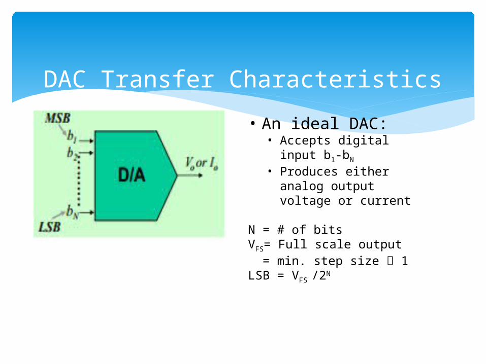
DAC Transfer Characteristics
• An ideal DAC:• Accepts digital input b1-
bN
• Produces either analog output voltage or current
N = # of bitsVFS= Full scale output = min. step size 1 LSB = VFS /2N
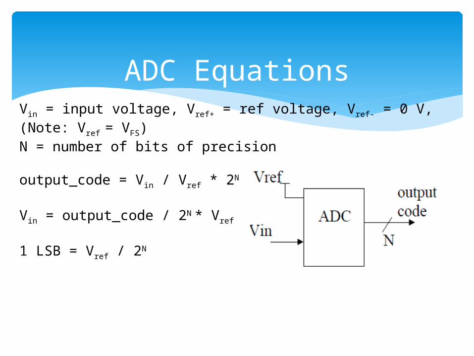
ADC EquationsVin = input voltage, Vref+ = ref voltage, Vref- = 0 V, (Note: Vref = VFS)N = number of bits of precision
output_code = Vin / Vref * 2N
Vin = output_code / 2N * Vref
1 LSB = Vref / 2N
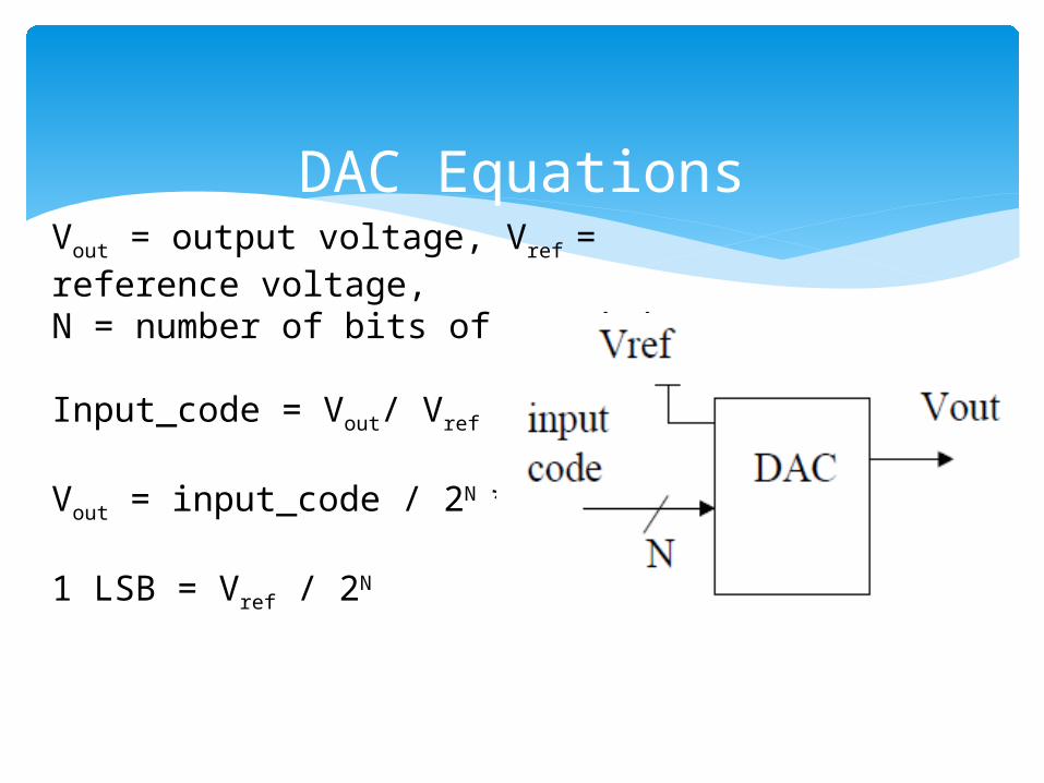
DAC EquationsVout = output voltage, Vref = reference voltage, N = number of bits of precision
Input_code = Vout/ Vref * 2N
Vout = input_code / 2N * Vref
1 LSB = Vref / 2N
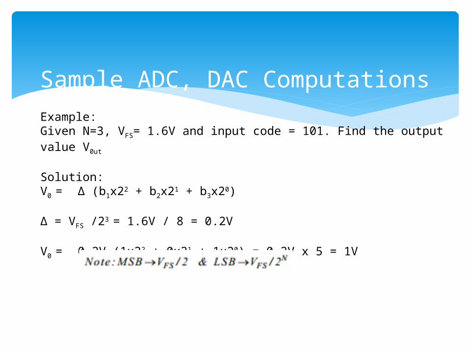
Sample ADC, DAC ComputationsExample: Given N=3, VFS= 1.6V and input code = 101. Find the output value V0ut
Solution:V0 = Δ (b1x22 + b2x21 + b3x20)
Δ = VFS /23 = 1.6V / 8 = 0.2V
V0 = 0.2V (1x22 + 0x21 + 1x20) = 0.2V x 5 = 1V
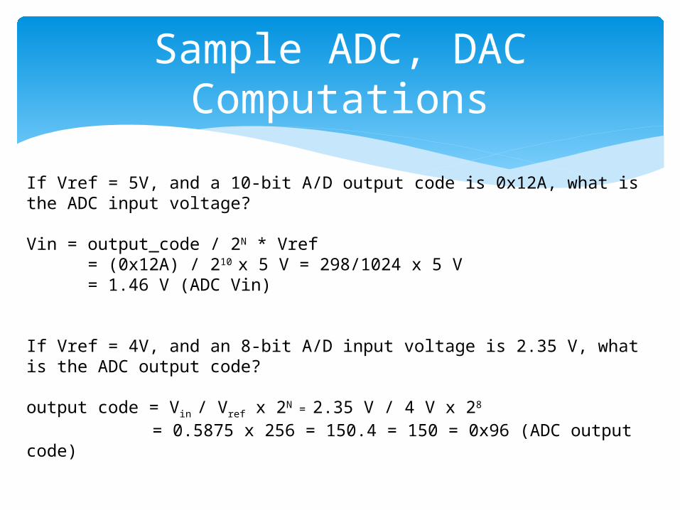
Sample ADC, DAC Computations
If Vref = 5V, and a 10-bit A/D output code is 0x12A, what is the ADC input voltage?
Vin = output_code / 2N * Vref = (0x12A) / 210 x 5 V = 298/1024 x 5 V = 1.46 V (ADC Vin)
If Vref = 4V, and an 8-bit A/D input voltage is 2.35 V, what is the ADC output code?
output code = Vin / Vref x 2N = 2.35 V / 4 V x 28
= 0.5875 x 256 = 150.4 = 150 = 0x96 (ADC output code)
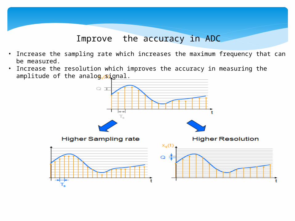
Improve the accuracy in ADC
• Increase the sampling rate which increases the maximum frequency that can be measured.
• Increase the resolution which improves the accuracy in measuring the amplitude of the analog signal.
References:http://www.ni.com/white-paper/4806/en/
Home > Products and Services > White Papers > Understanding Resolution in High-Speed Digitizers/Oscilloscopes
http://inst.eecs.berkeley.edu/~ee247/fa10/files07/lectures/L11_2_f10.pdf
http://194.81.104.27/~brian/DSP/ADC_notes.pdf
ume.gatech.edu/mechatronics_course/ADC_F10.pptx


![[SJSU] Social Media Strategy](https://img.pdfslide.net/doc/110x75/559793dc1a28abdd108b467c/sjsu-social-media-strategy.jpg)